rt2875 3a automotive buck converter - richtek.com/media/an pdf/an047_en.pdf · rt2875 3a automotive...
TRANSCRIPT
Application Note Roland van Roy
AN047 – March 2016
AN047 © 2016 Richtek Technology Corporation 1
RT2875 3A Automotive Buck Converter
Abstract
Designing a DC/DC buck converter for automotive applications requires special care of several conditions that are specific for
automotive environment : The very wide operating temperature range, input voltage fluctuations and stringent requirements
on EMI/noise generation due to the nearby car radio receiver. This application note describes the design of buck voltage
regulators for automotive environment using the RT2875BQGCP, a 36V/3A AEC-Q100 grade-2 qualified buck converter IC.
The Richtek Designer™ tool is used for initial design and component value selections.
CONTENTS 1. Introduction ............................................................................................................................................. 2
2. Challenges of Automotive environment .................................................................................................... 2
3. RT2875BQGCP features overview ............................................................................................................. 3
4. RT2875 family .......................................................................................................................................... 4
5. RT2875 design considerations................................................................................................................... 4
6. Practical RT2875 application example ....................................................................................................... 6
Application example : 5.0V/1.5A system supply......................................................................................... 6
RLIM value .................................................................................................................................................. 8
Load transient performance and Loop stability design. ............................................................................ 11
Converter power loss, efficiency and thermal design ............................................................................... 17
Application EMI considerations ............................................................................................................... 20
7. Layout example ...................................................................................................................................... 23
8. Other application tips ............................................................................................................................. 23
Using the external sync function ............................................................................................................. 23
Bootstrap capacitor charging circuit ........................................................................................................ 26
9. Conclusion.............................................................................................................................................. 28
RT2875 3A Automotive Buck Converter
AN047 © 2016 Richtek Technology Corporation 2
1. INTRODUCTION Automotive environment can be quite harsh and designing electronics that need to work reliable in this environment takes special care, and often requires automotive qualified parts. When designing voltage regulators that need to step down an intermediate voltage from the car battery supply, the car battery voltage fluctuation needs to be taken into regard. The full operating temperature range needs to be considered for all aspects of the design, and all component parameters have to be checked over temperature. The car radio receiver is nearby, which means that any switch-mode converter radiated emission needs to be minimized to avoid switch noise being coupled into the car radio receiver. Richtek has released several new parts for automotive applications which are AEC-Q100 qualified. The following chapters describe how to design intermediate power rails from car battery supply using RT2875BQGCP, an AEC-Q100 grade-2 qualified 36V/3A current mode buck converter.
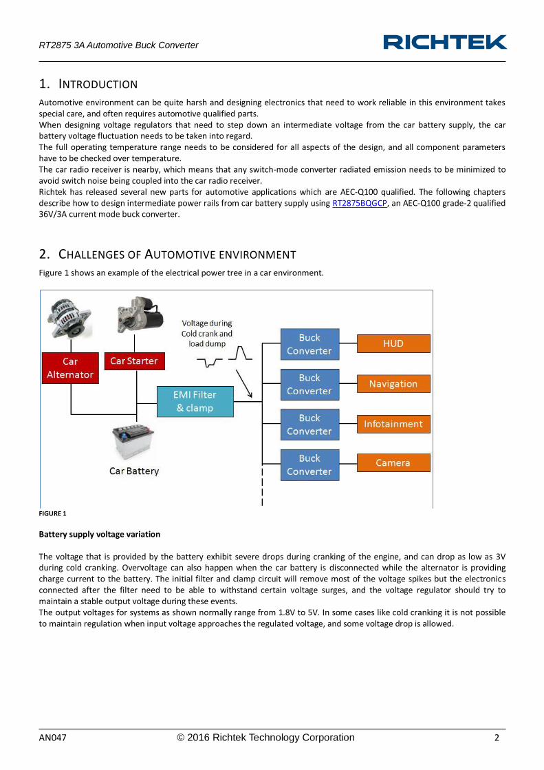
2. CHALLENGES OF AUTOMOTIVE ENVIRONMENT Figure 1 shows an example of the electrical power tree in a car environment.
FIGURE 1
Battery supply voltage variation The voltage that is provided by the battery exhibit severe drops during cranking of the engine, and can drop as low as 3V during cold cranking. Overvoltage can also happen when the car battery is disconnected while the alternator is providing charge current to the battery. The initial filter and clamp circuit will remove most of the voltage spikes but the electronics connected after the filter need to be able to withstand certain voltage surges, and the voltage regulator should try to maintain a stable output voltage during these events. The output voltages for systems as shown normally range from 1.8V to 5V. In some cases like cold cranking it is not possible to maintain regulation when input voltage approaches the regulated voltage, and some voltage drop is allowed.
RT2875 3A Automotive Buck Converter
AN047 © 2016 Richtek Technology Corporation 3
EMI All switch mode converters generate some EMI. The amount of radiation depends on switching frequency, converter switching speed, load current, filtering, and layout. A radio receiver nearby has high sensitivity in electromagnetic fields in its operating bands, and will easily be affected by converter switch noise. Selecting a suitable switching frequency can help to avoid radiating noise in sensitive frequency bands. Reducing switching speed can reduce EMI as well, but often reduced switch speed increases the converter switch losses which reduces efficiency. Good filtering and PCB layout are extremely important for minimizing noise to external circuits. Wide operating temperature range The temperature range in automotive environment can range from extreme cold when the car is outside in wintertime to very hot when the car is outside in the sun in summer time. All electronic components will exhibit parameter drift over temperature, so critical operation modes need to be carefully checked in different temperature conditions to ensure correct operation over the full temperature range. For this reason many automotive qualified IC parameters are fully characterized over temperature, so designers can use this data to examine worst case conditions.
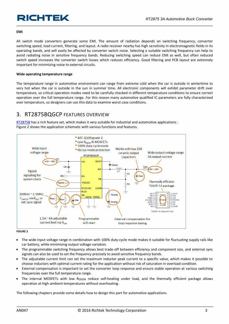
3. RT2875BQGCP FEATURES OVERVIEW RT2875B has a rich feature set, which makes it very suitable for industrial and automotive applications : Figure 2 shows the application schematic with various functions and features.
FIGURE 2
The wide input voltage range in combination with 100% duty-cycle mode makes it suitable for fluctuating supply rails like car battery, while minimizing output voltage variation.
The programmable switching frequency allows best trade-off between efficiency and component size, and external sync signals can also be used to set the frequency precisely to avoid sensitive frequency bands.
The adjustable current limit can set the maximum inductor peak current to a specific value, which makes it possible to choose inductors with optimal current rating for the application without risk of saturation in overload condition.
External compensation is important to set the converter loop response and ensure stable operation at various switching frequencies over the full temperature range.
The internal MOSFETs with low RDSON reduce self-heating under load, and the thermally efficient package allows operation at high ambient temperatures without overheating.
The following chapters provide some details how to design this part for automotive applications.
RT2875 3A Automotive Buck Converter
AN047 © 2016 Richtek Technology Corporation 4
4. RT2875 FAMILY There are three parts in the RT2875 family :
RT2875AQGCP with 2% reference voltage accuracy and latch-off UVP protection
RT2875BQGCP with 2% reference voltage accuracy and hiccup UVP protection
RT2875DQGCP with 1% reference voltage accuracy and hiccup UVP protection Whether to choose Latch-off or hiccup mode protection depends on user preference. Latch-off UVP protection always needs system intervention to reset the converter (via enable pin) after an output under-voltage condition has been triggered. Hiccup mode UVP protection devices will automatically try to recover from output under-voltage condition. The hiccup mode will ensure low power consumption in continuous overload. In most applications, hiccup mode is the preferred protection mode. If very high output accuracy is needed, RT2875D may be the best choice, but for most applications 2% reference accuracy (over the full temperature range) will be sufficient.
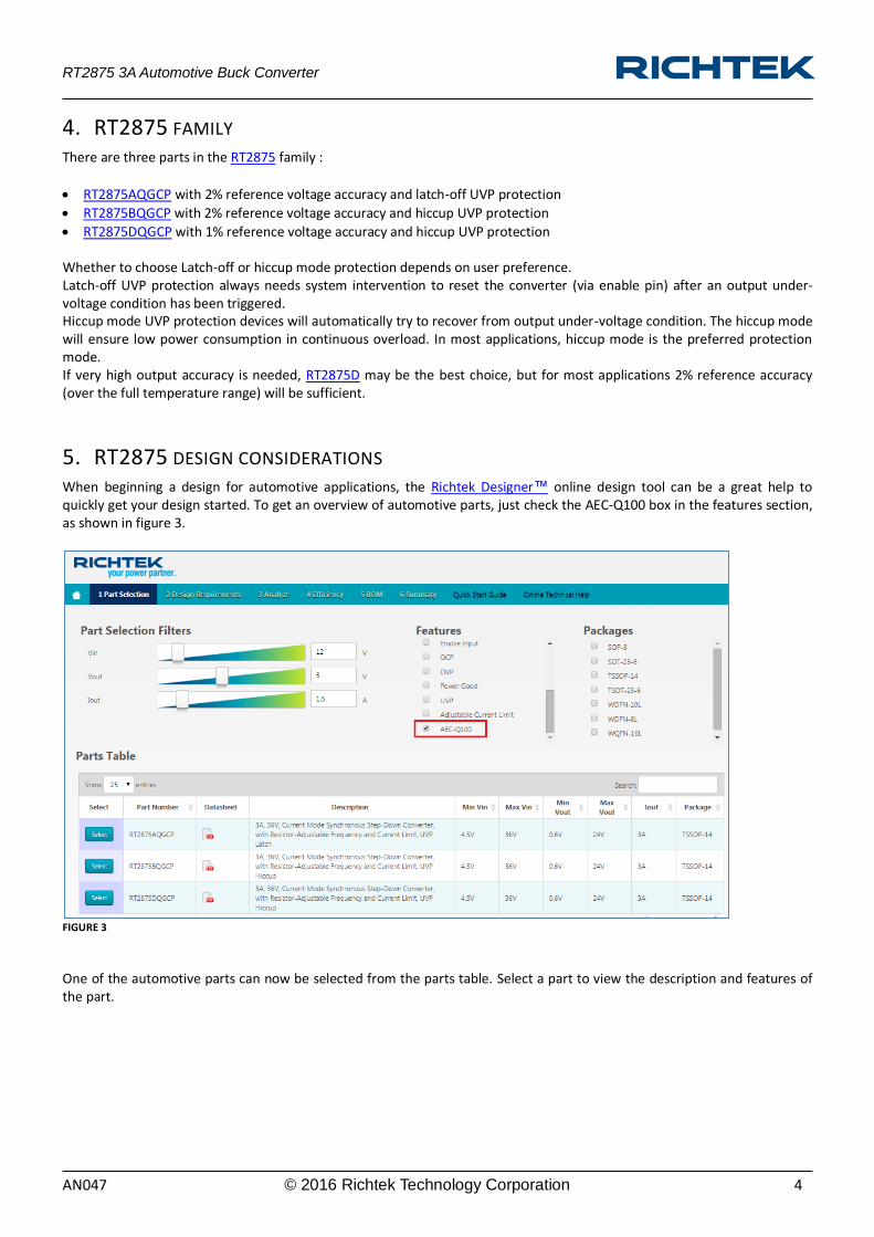
5. RT2875 DESIGN CONSIDERATIONS When beginning a design for automotive applications, the Richtek Designer™ online design tool can be a great help to quickly get your design started. To get an overview of automotive parts, just check the AEC-Q100 box in the features section, as shown in figure 3.
FIGURE 3
One of the automotive parts can now be selected from the parts table. Select a part to view the description and features of the part.

RT2875 3A Automotive Buck Converter
AN047 © 2016 Richtek Technology Corporation 5
After selecting a part, the menu will show the design requirements page. See figure 4.
FIGURE 4
Input voltage range, output voltage and load current are normally defined by the application. For RT2875, switching frequency and inductor peak inductor current limit can be set via external resistors. There are some things to consider when setting these parameters : Switching frequency considerations : Selecting higher switching frequency will reduce output voltage ripple, allow lower inductance values and increase the converter bandwidth for faster reaction on load transients. But it will also increase switch losses, especially at higher input voltages. The higher switching frequency will also limit the minimum and maximum duty-cycles that can be achieved :
δmin = tON min∙FSW (RT2875 tON min ≈ 100nsec)
δmax = 1 - tOFF min∙FSW (RT2875 tOFF min ≈ 100nsec)
Converter duty-cycle δ is determined by VOUT/VIN.
Applications with high step down ratio and high switching frequency setting will quickly hit the minimum duty-cycle limit, and RT2875 will start to skip pulses to maintain regulated output voltage. But output ripple will increase in pulse skip operation due to pulse grouping, so this operation mode should generally be avoided. The design tool will give a warning message when selecting parameters which result in hitting minimum duty-cycle limit. If this is the case, a lower switching frequency should be chosen.
Operation where VIN is close to VOUT can result in maximum duty-cycle operation. Again, RT2875 will start skipping pulses to maintain regulation, gradually moving to 100% duty-cycle mode, but pulse grouping will increase output ripple. Lowering the switching frequency can help here as well but higher output voltage supplies will often encounter this mode in automotive
applications during cold-cranking, when VIN drops to very low levels. Output voltage regulation will be maintained until 100% duty-cycle mode is reached. Peak inductor current limit considerations : This parameter can be used to set the limit of the maximum peak current in the inductor. This can be helpful in applications that don’t require high load currents. In these cases, the designer can set a suitable low peak current value and choose an inductor with a lower saturation current as well, which can then be a smaller (cheaper) type. Even overload conditions will not result in larger peak current than the set value, so inductor saturation is avoided.
The maximum load current that can be achieved during peak current limiting is always ½ IRIPPLE pp lower than the actual peak current limit, because the load current is the average value of the inductor current, which includes the current ripple. See figure 5.
FIGURE 5 : RELATION BETWEEN PEAK CURRENT LIMIT AND MAX LOAD CURRENT

RT2875 3A Automotive Buck Converter
AN047 © 2016 Richtek Technology Corporation 6
It should be noted that the peak inductor current limit as shown in the design requirement box is a typical value : The IC datasheet should be checked for tolerances, to ensure that current limit at minimum tolerance will be sufficient to supply the
required load current. Due to IC propagation delays, the actual current limit is also dependent on VIN, VOUT and inductance value. The design tool can be used to verify the actual current limit for the specific application, which matches the real IC current limit behavior quite accurately.
6. PRACTICAL RT2875 APPLICATION EXAMPLE
APPLICATION EXAMPLE : 5.0V/1.5A SYSTEM SUPPLY.
Input voltage range : 13.5V typical, minimum 6V during engine cranking and maximum 28V during load dump. Switching frequency preferred at 2.1MHz to minimize noise in the AM radio band. Maximum load step is 1App. Ambient operation range : -30°C ~ +70°C, hiccup mode protection is preferred. Output voltage tolerance is 5V±5% over the full temperature range. For this application, RT2875BQGCP is a suitable choice. Application checks :
For 2.1MHz switching frequency, the duty-cycle where minimum on time is reached lies at 21% and the duty-cycle where
minimum off time is reached lies at 79%. So at 28V input, some pulse skipping will occur, and VIN below 6.3V will result in
pulse skipping as well. At 5V input, the converter will work in 100% duty-cycle mode, and VOUT will slightly drop. But at nominal input of 13.5V, the converter will not have any duty-cycle limitations.
The 1.5A maximum load is well below the converter rated current, and IC dissipation will be relatively low, even at the high switching frequency.
It is possible to make use of the peak current limit function to set a peak current which is sufficient to guarantee 1.5A load. We’ll use Richtek Designer to provide the required component values for this design.
FIGURE 6
To start the design, we use Richtek Designer, select RT2875BQ. In the Design Requirements section the typical operation values are entered. (When entering different values for Vin Min and Vin Max, the tool will use the average Vin value to calculate component values). The current limit setting is first kept at the default value, it will be modified later. See figure 6. After clicking Create Design, the tool will generate the full schematic with all component values.
RT2875 3A Automotive Buck Converter
AN047 © 2016 Richtek Technology Corporation 7
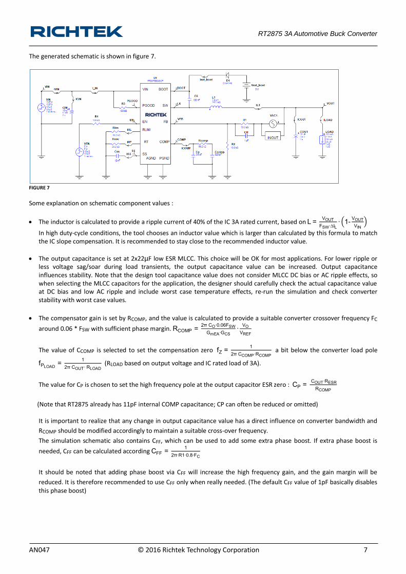
The generated schematic is shown in figure 7.
FIGURE 7
Some explanation on schematic component values :
The inductor is calculated to provide a ripple current of 40% of the IC 3A rated current, based on L = VOUT
FSW∙∆IL∙ (1-
VOUT
VIN)
In high duty-cycle conditions, the tool chooses an inductor value which is larger than calculated by this formula to match the IC slope compensation. It is recommended to stay close to the recommended inductor value.
The output capacitance is set at 2x22µF low ESR MLCC. This choice will be OK for most applications. For lower ripple or less voltage sag/soar during load transients, the output capacitance value can be increased. Output capacitance influences stability. Note that the design tool capacitance value does not consider MLCC DC bias or AC ripple effects, so when selecting the MLCC capacitors for the application, the designer should carefully check the actual capacitance value at DC bias and low AC ripple and include worst case temperature effects, re-run the simulation and check converter stability with worst case values.
The compensator gain is set by RCOMP, and the value is calculated to provide a suitable converter crossover frequency FC
around 0.06 * FSW with sufficient phase margin. RCOMP = 2π CO∙0.06FSW
GmEA∙GCS∙
VO
VREF
The value of CCOMP is selected to set the compensation zero fZ = 1
2π CCOMP∙RCOMP a bit below the converter load pole
fPLOAD =
1
2π COUT∙ RLOAD (RLOAD based on output voltage and IC rated load of 3A).
The value for CP is chosen to set the high frequency pole at the output capacitor ESR zero : CP = COUT∙RESR
RCOMP
(Note that RT2875 already has 11pF internal COMP capacitance; CP can often be reduced or omitted) It is important to realize that any change in output capacitance value has a direct influence on converter bandwidth and
RCOMP should be modified accordingly to maintain a suitable cross-over frequency.
The simulation schematic also contains CFF, which can be used to add some extra phase boost. If extra phase boost is
needed, CFF can be calculated according CFF = 1
2π∙R1∙0.8∙FC
It should be noted that adding phase boost via CFF will increase the high frequency gain, and the gain margin will be
reduced. It is therefore recommended to use CFF only when really needed. (The default CFF value of 1pF basically disables this phase boost)
RT2875 3A Automotive Buck Converter
AN047 © 2016 Richtek Technology Corporation 8
The default soft-start capacitor is set at 10nF, which gives a soft-start time of 1msec.
The schematic also shows an external circuit (Vext_boot and D1) which charges the bootstrap capacitor C6. Although RT2875 includes an internal bootstrap charging circuit, the external circuit is recommended for automotive applications with output voltages equal or greater than 3.3V. The external charge circuit will ensure correct bootstrap capacitor
charging at all duty-cycle conditions, including the high duty-cycle transition to 100% mode when VIN drops very close to
VOUT, and it will also increase converter efficiency.
For applications with VOUT ranging from 3.3V ~ 5V, the bootstrap charge supply can actually be taken from VOUT. (D1 should
preferably be a Schottky when VOUT is 3.3V). When VOUT is higher than 5V, the bootstrap charge supply can be derived from
VOUT via a resistor divider and buffer capacitor. The measured current Iext_boot can be used to check the required current for charging the bootstrap capacitor.
Richtek Designer simulation allows you to check many effects, like start-up & shut-down from VIN or Enable, VOUT ripple and
VOUT fluctuations during load transient, current limiting when exceeding maximum load, VIN rising or falling to check pulse skipping and 100% duty-cycle mode, loop stability via load transient or gain-phase analysis, and efficiency and power loss. The BOM generation section will show some suggestions for component choices.
RLIM VALUE
To determine the optimal RLIM value which will guarantee load capability over the full operation range, we need to check the inductor peak current at maximum load and then select a peak current limit that matches this peak current but will not trigger the protection in worst case condition.
Inductor ripple is determined by : ∆IL = VOUT
FSW∙L∙ (1-
VOUT
VIN)
For our example application we’ll use a standard 1µH inductor, nominal VIN voltage of 13.5V. At nominal frequency this will give a current ripple of 1.5App. The worst case peak current will be 1.5A DC load + 0.5 * 1.5App = 2.25A. The IC current limit must be well above this value to avoid unwanted triggering of peak current limit. It is recommended to use a peak current setting which is at least 50% higher than the nominal operation peak current, so our recommended peak current limit will become 2.25 * 1.5 = 3.37A. This extra margin is needed to cover several tolerances, like IC frequency tolerance and current limit tolerance, but also the effect of
different VIN conditions, especially when the application operation enters pulse skipping at minimum off time (low VIN) conditions: In pulse skipping, the operation frequency changes abruptly and peak current would be higher than normal
operation, and the current limiting here can quickly cause VOUT drop. Although operation at higher VIN conditions would
seem worst case due to increase the current ripple, the higher VIN also increases the inductor current rising slope dI/dt, and the IC current limit circuit propagation delay will extend the current limit as well, actually compensating for the increased current ripple.
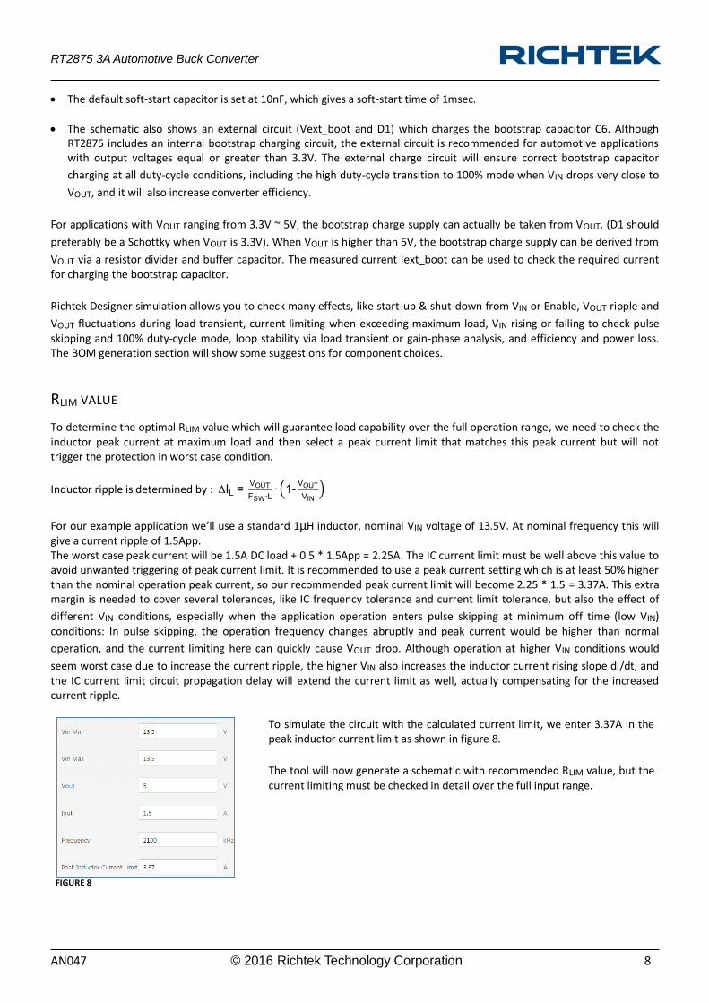
FIGURE 8
To simulate the circuit with the calculated current limit, we enter 3.37A in the peak inductor current limit as shown in figure 8.
The tool will now generate a schematic with recommended RLIM value, but the current limiting must be checked in detail over the full input range.
RT2875 3A Automotive Buck Converter
AN047 © 2016 Richtek Technology Corporation 9
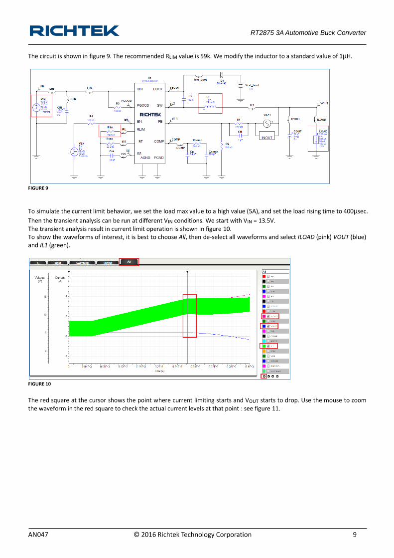
The circuit is shown in figure 9. The recommended RLIM value is 59k. We modify the inductor to a standard value of 1µH.
FIGURE 9
To simulate the current limit behavior, we set the load max value to a high value (5A), and set the load rising time to 400µsec.
Then the transient analysis can be run at different VIN conditions. We start with VIN = 13.5V. The transient analysis result in current limit operation is shown in figure 10. To show the waveforms of interest, it is best to choose All, then de-select all waveforms and select ILOAD (pink) VOUT (blue) and IL1 (green).
FIGURE 10
The red square at the cursor shows the point where current limiting starts and VOUT starts to drop. Use the mouse to zoom the waveform in the red square to check the actual current levels at that point : see figure 11.
RT2875 3A Automotive Buck Converter
AN047 © 2016 Richtek Technology Corporation 10
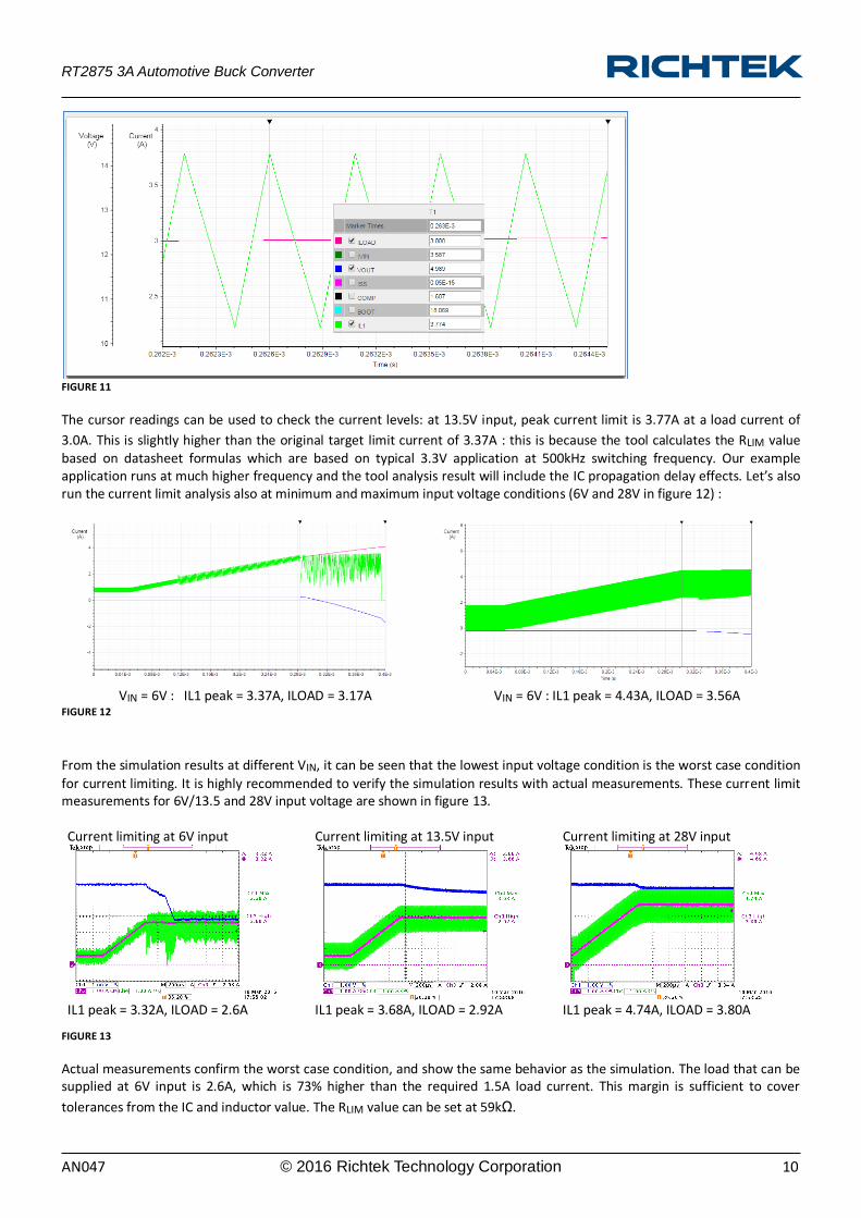
FIGURE 11
The cursor readings can be used to check the current levels: at 13.5V input, peak current limit is 3.77A at a load current of
3.0A. This is slightly higher than the original target limit current of 3.37A : this is because the tool calculates the RLIM value based on datasheet formulas which are based on typical 3.3V application at 500kHz switching frequency. Our example application runs at much higher frequency and the tool analysis result will include the IC propagation delay effects. Let’s also run the current limit analysis also at minimum and maximum input voltage conditions (6V and 28V in figure 12) :
VIN = 6V : IL1 peak = 3.37A, ILOAD = 3.17A VIN = 6V : IL1 peak = 4.43A, ILOAD = 3.56A
FIGURE 12
From the simulation results at different VIN, it can be seen that the lowest input voltage condition is the worst case condition
for current limiting. It is highly recommended to verify the simulation results with actual measurements. These current limit measurements for 6V/13.5 and 28V input voltage are shown in figure 13. Current limiting at 6V input Current limiting at 13.5V input Current limiting at 28V input
IL1 peak = 3.32A, ILOAD = 2.6A IL1 peak = 3.68A, ILOAD = 2.92A IL1 peak = 4.74A, ILOAD = 3.80A
FIGURE 13
Actual measurements confirm the worst case condition, and show the same behavior as the simulation. The load that can be supplied at 6V input is 2.6A, which is 73% higher than the required 1.5A load current. This margin is sufficient to cover
tolerances from the IC and inductor value. The RLIM value can be set at 59kΩ.
RT2875 3A Automotive Buck Converter
AN047 © 2016 Richtek Technology Corporation 11
The maximum peak current that can occur happens at maximum input voltage. When we include IC tolerances, the worst case peak current would be around 15% higher than the measured value of 4.74A to become 5.5A. Inductor saturation current would need to be higher than this value to avoid saturation effects at worst case overload conditions.
For testing the design a Wuerth Electronic 74437321010 1µH, IRMS = 3.5A, RDC = 41mΩ, ISAT = 7A shielded inductor was chosen.
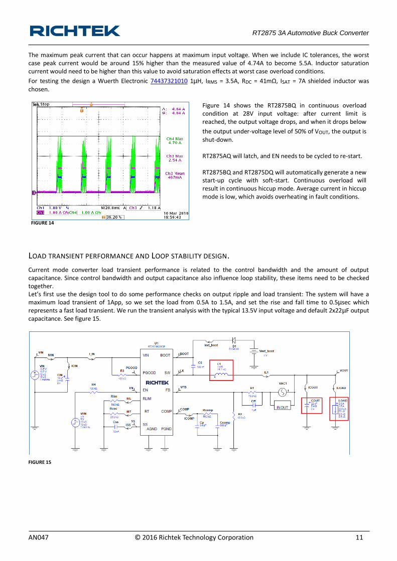
FIGURE 14
Figure 14 shows the RT2875BQ in continuous overload condition at 28V input voltage: after current limit is reached, the output voltage drops, and when it drops below
the output under-voltage level of 50% of VOUT, the output is shut-down. RT2875AQ will latch, and EN needs to be cycled to re-start. RT2875BQ and RT2875DQ will automatically generate a new start-up cycle with soft-start. Continuous overload will result in continuous hiccup mode. Average current in hiccup mode is low, which avoids overheating in fault conditions.
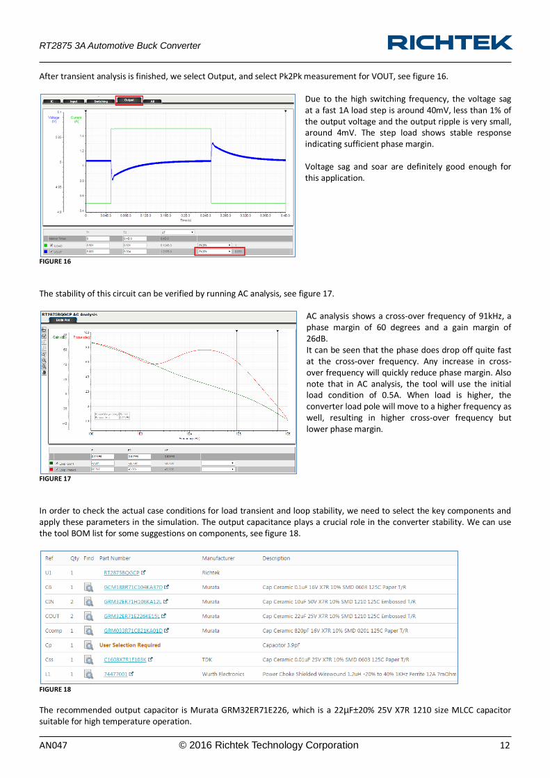
LOAD TRANSIENT PERFORMANCE AND LOOP STABILITY DESIGN.
Current mode converter load transient performance is related to the control bandwidth and the amount of output capacitance. Since control bandwidth and output capacitance also influence loop stability, these items need to be checked together. Let’s first use the design tool to do some performance checks on output ripple and load transient: The system will have a maximum load transient of 1App, so we set the load from 0.5A to 1.5A, and set the rise and fall time to 0.5µsec which represents a fast load transient. We run the transient analysis with the typical 13.5V input voltage and default 2x22µF output capacitance. See figure 15.
FIGURE 15
RT2875 3A Automotive Buck Converter
AN047 © 2016 Richtek Technology Corporation 12
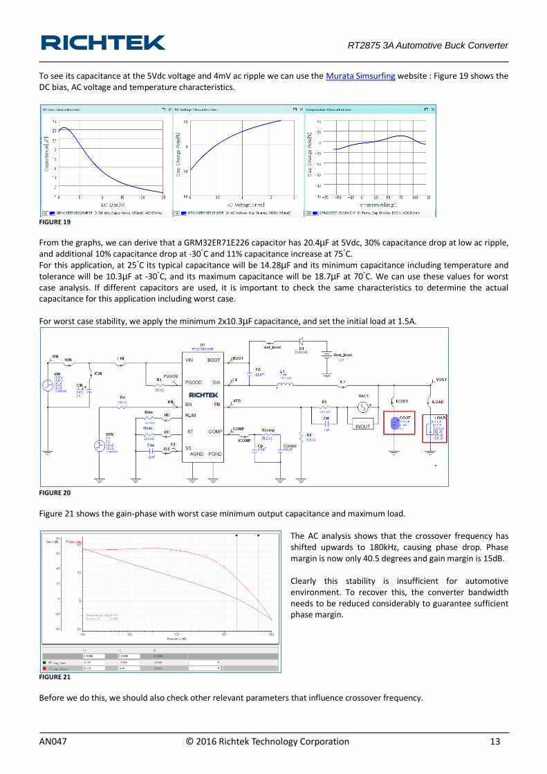
After transient analysis is finished, we select Output, and select Pk2Pk measurement for VOUT, see figure 16.
FIGURE 16
Due to the high switching frequency, the voltage sag at a fast 1A load step is around 40mV, less than 1% of the output voltage and the output ripple is very small, around 4mV. The step load shows stable response indicating sufficient phase margin. Voltage sag and soar are definitely good enough for this application.
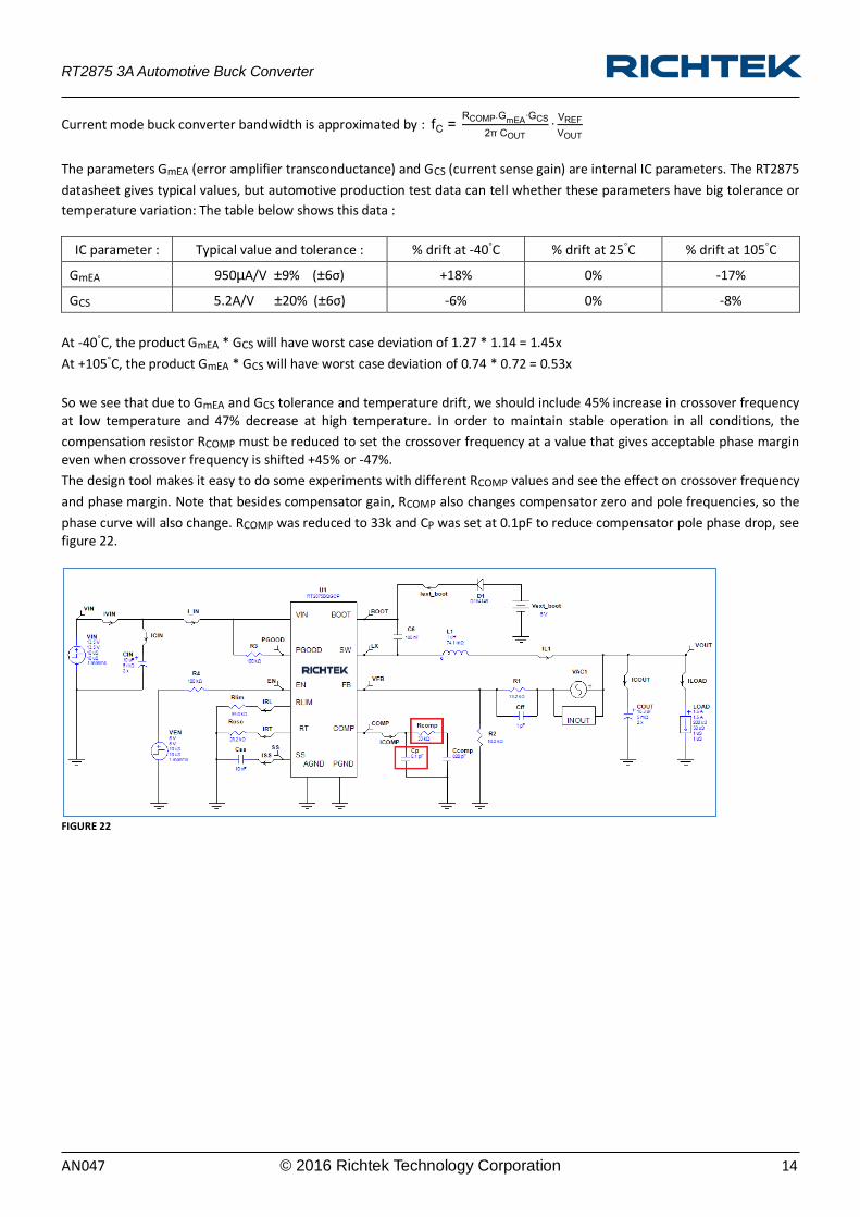
The stability of this circuit can be verified by running AC analysis, see figure 17.
FIGURE 17
AC analysis shows a cross-over frequency of 91kHz, a phase margin of 60 degrees and a gain margin of 26dB. It can be seen that the phase does drop off quite fast at the cross-over frequency. Any increase in cross-over frequency will quickly reduce phase margin. Also note that in AC analysis, the tool will use the initial load condition of 0.5A. When load is higher, the converter load pole will move to a higher frequency as well, resulting in higher cross-over frequency but lower phase margin.
In order to check the actual case conditions for load transient and loop stability, we need to select the key components and apply these parameters in the simulation. The output capacitance plays a crucial role in the converter stability. We can use the tool BOM list for some suggestions on components, see figure 18.
FIGURE 18
The recommended output capacitor is Murata GRM32ER71E226, which is a 22µF±20% 25V X7R 1210 size MLCC capacitor suitable for high temperature operation.
RT2875 3A Automotive Buck Converter
AN047 © 2016 Richtek Technology Corporation 13
To see its capacitance at the 5Vdc voltage and 4mV ac ripple we can use the Murata Simsurfing website : Figure 19 shows the DC bias, AC voltage and temperature characteristics.
FIGURE 19
From the graphs, we can derive that a GRM32ER71E226 capacitor has 20.4µF at 5Vdc, 30% capacitance drop at low ac ripple, and additional 10% capacitance drop at -30°C and 11% capacitance increase at 75°C. For this application, at 25°C its typical capacitance will be 14.28µF and its minimum capacitance including temperature and tolerance will be 10.3µF at -30°C, and its maximum capacitance will be 18.7µF at 70°C. We can use these values for worst case analysis. If different capacitors are used, it is important to check the same characteristics to determine the actual capacitance for this application including worst case. For worst case stability, we apply the minimum 2x10.3µF capacitance, and set the initial load at 1.5A.
FIGURE 20
Figure 21 shows the gain-phase with worst case minimum output capacitance and maximum load.
FIGURE 21
The AC analysis shows that the crossover frequency has shifted upwards to 180kHz, causing phase drop. Phase margin is now only 40.5 degrees and gain margin is 15dB. Clearly this stability is insufficient for automotive environment. To recover this, the converter bandwidth needs to be reduced considerably to guarantee sufficient phase margin.
Before we do this, we should also check other relevant parameters that influence crossover frequency.
RT2875 3A Automotive Buck Converter
AN047 © 2016 Richtek Technology Corporation 14
Current mode buck converter bandwidth is approximated by : fC = RCOMP∙GmEA
∙GCS
2π COUT∙
VREF
VOUT
The parameters GmEA (error amplifier transconductance) and GCS (current sense gain) are internal IC parameters. The RT2875
datasheet gives typical values, but automotive production test data can tell whether these parameters have big tolerance or
temperature variation: The table below shows this data :
IC parameter : Typical value and tolerance : % drift at -40°C % drift at 25°C % drift at 105°C
GmEA 950µA/V ±9% (±6σ) +18% 0% -17%
GCS 5.2A/V ±20% (±6σ) -6% 0% -8%
At -40°C, the product GmEA * GCS will have worst case deviation of 1.27 * 1.14 = 1.45x
At +105°C, the product GmEA * GCS will have worst case deviation of 0.74 * 0.72 = 0.53x
So we see that due to GmEA and GCS tolerance and temperature drift, we should include 45% increase in crossover frequency at low temperature and 47% decrease at high temperature. In order to maintain stable operation in all conditions, the
compensation resistor RCOMP must be reduced to set the crossover frequency at a value that gives acceptable phase margin even when crossover frequency is shifted +45% or -47%.
The design tool makes it easy to do some experiments with different RCOMP values and see the effect on crossover frequency
and phase margin. Note that besides compensator gain, RCOMP also changes compensator zero and pole frequencies, so the
phase curve will also change. RCOMP was reduced to 33k and CP was set at 0.1pF to reduce compensator pole phase drop, see figure 22.
FIGURE 22
RT2875 3A Automotive Buck Converter
AN047 © 2016 Richtek Technology Corporation 15
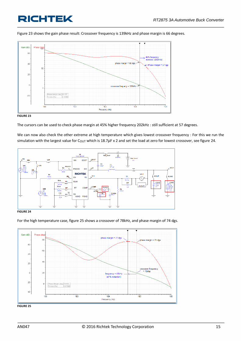
Figure 23 shows the gain phase result: Crossover frequency is 139kHz and phase margin is 66 degrees.
FIGURE 23
The cursors can be used to check phase margin at 45% higher frequency 202kHz : still sufficient at 57 degrees. We can now also check the other extreme at high temperature which gives lowest crossover frequency : For this we run the
simulation with the largest value for COUT which is 18.7µF x 2 and set the load at zero for lowest crossover, see figure 24.
FIGURE 24
For the high temperature case, figure 25 shows a crossover of 78kHz, and phase margin of 74 dgs.
FIGURE 25
RT2875 3A Automotive Buck Converter
AN047 © 2016 Richtek Technology Corporation 16
Applying 47% frequency reduction due to IC high temperature condition shows that phase margin will not become worse.
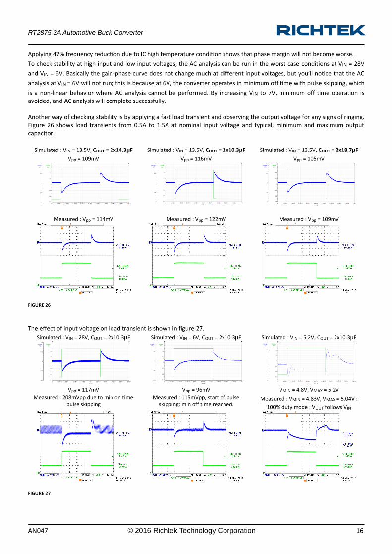
To check stability at high input and low input voltages, the AC analysis can be run in the worst case conditions at VIN = 28V
and VIN = 6V. Basically the gain-phase curve does not change much at different input voltages, but you’ll notice that the AC
analysis at VIN = 6V will not run; this is because at 6V, the converter operates in minimum off time with pulse skipping, which
is a non-linear behavior where AC analysis cannot be performed. By increasing VIN to 7V, minimum off time operation is avoided, and AC analysis will complete successfully. Another way of checking stability is by applying a fast load transient and observing the output voltage for any signs of ringing. Figure 26 shows load transients from 0.5A to 1.5A at nominal input voltage and typical, minimum and maximum output capacitor.
Simulated : VIN = 13.5V, COUT = 2x14.3µF Simulated : VIN = 13.5V, COUT = 2x10.3µF Simulated : VIN = 13.5V, COUT = 2x18.7µF
Vpp = 109mV Vpp = 116mV Vpp = 105mV
Measured : Vpp = 114mV Measured : Vpp = 122mV Measured : Vpp = 109mV
FIGURE 26
The effect of input voltage on load transient is shown in figure 27.
Simulated : VIN = 28V, COUT = 2x10.3µF Simulated : VIN = 6V, COUT = 2x10.3µF Simulated : VIN = 5.2V, COUT = 2x10.3µF
Vpp = 117mV Vpp = 96mV VMIN = 4.8V, VMAX = 5.2V
Measured : 208mVpp due to min on time pulse skipping
Measured : 115mVpp, start of pulse skipping: min off time reached.
Measured : VMIN = 4.83V, VMAX = 5.04V :
100% duty mode : VOUT follows VIN
FIGURE 27
RT2875 3A Automotive Buck Converter
AN047 © 2016 Richtek Technology Corporation 17
At 28V input and 0.5A load, minimum on-time pulse skipping results in higher output ripple than the simulation model can show. The key-point is that minimum on-time pulse skipping should not be confused with unstable control loop. It can also
be seen that when VIN is very low, the converter will go into 100% duty-cycle mode during high load, and output voltage
regulation is not possible anymore. VOUT follows VIN, minus converter RDSON drop and inductor DCR drop. Any ringing here is caused by the inductor and output capacitor resonance, and should not be mistaken for instability. The actual measurement
100% duty VOUT waveform is slightly different from the model, because the model assumes an ideal input voltage source, whereas the actual measurement input voltage shows some sag during load transient, which is reflected to the output as well.
Figure 28 shows VIN drop from 13V to 5.4V, 5.1V and 4.7V respectively. (Pink : VIN, Blue : VOUT, Cyan : Switching)
Pulse skipping but no VOUT drop 100% duty, some VOUT drop 100% duty, VOUT 0.2V lower than VIN
FIGURE 28
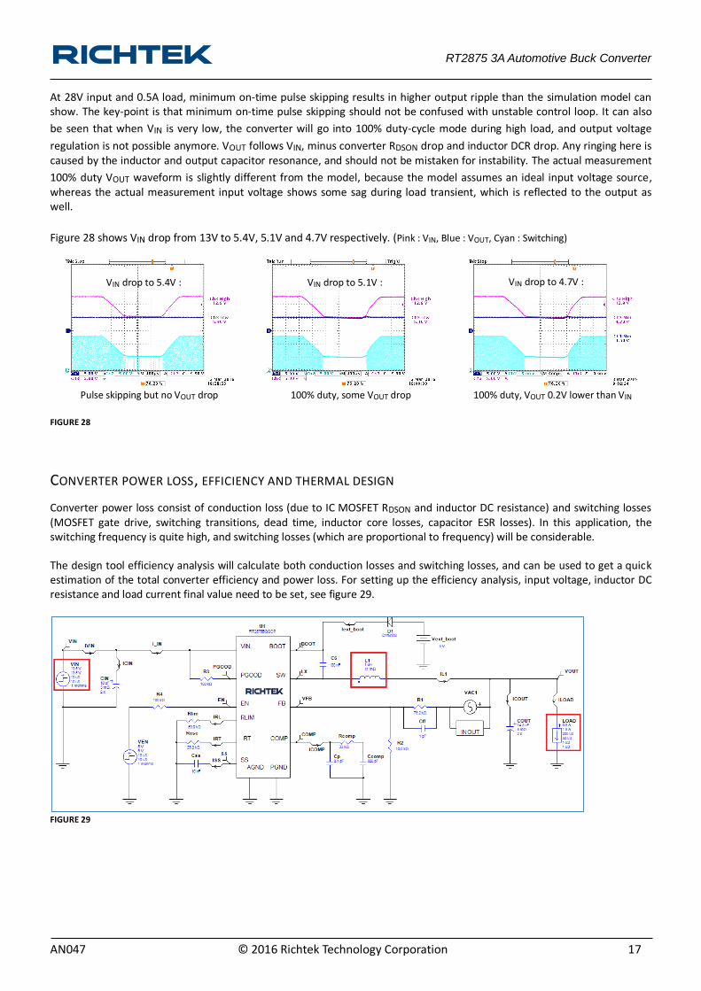
CONVERTER POWER LOSS, EFFICIENCY AND THERMAL DESIGN
Converter power loss consist of conduction loss (due to IC MOSFET RDSON and inductor DC resistance) and switching losses (MOSFET gate drive, switching transitions, dead time, inductor core losses, capacitor ESR losses). In this application, the switching frequency is quite high, and switching losses (which are proportional to frequency) will be considerable. The design tool efficiency analysis will calculate both conduction losses and switching losses, and can be used to get a quick estimation of the total converter efficiency and power loss. For setting up the efficiency analysis, input voltage, inductor DC resistance and load current final value need to be set, see figure 29.
FIGURE 29
VIN drop to 5.4V : VIN drop to 5.1V : VIN drop to 4.7V :
RT2875 3A Automotive Buck Converter
AN047 © 2016 Richtek Technology Corporation 18
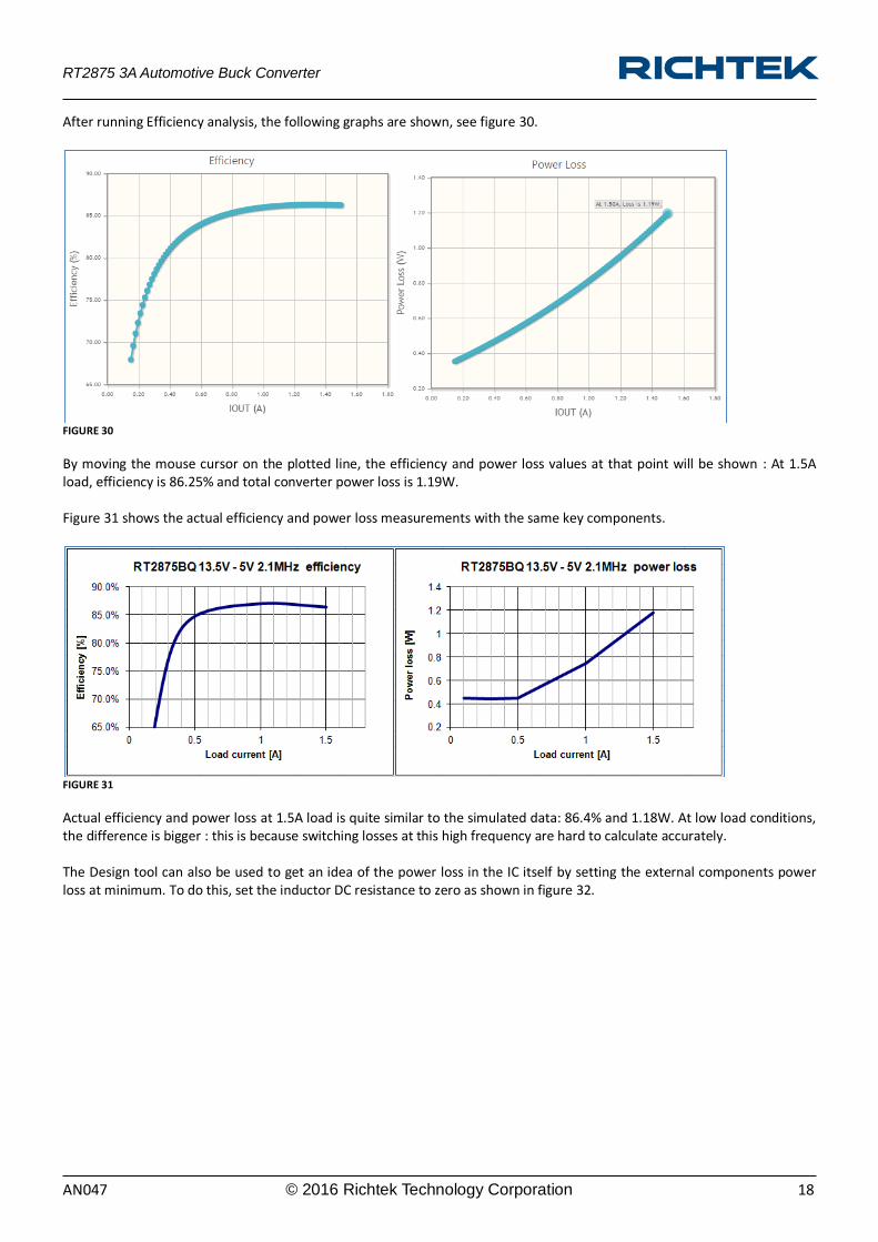
After running Efficiency analysis, the following graphs are shown, see figure 30.
FIGURE 30
By moving the mouse cursor on the plotted line, the efficiency and power loss values at that point will be shown : At 1.5A load, efficiency is 86.25% and total converter power loss is 1.19W. Figure 31 shows the actual efficiency and power loss measurements with the same key components.
FIGURE 31
Actual efficiency and power loss at 1.5A load is quite similar to the simulated data: 86.4% and 1.18W. At low load conditions, the difference is bigger : this is because switching losses at this high frequency are hard to calculate accurately. The Design tool can also be used to get an idea of the power loss in the IC itself by setting the external components power loss at minimum. To do this, set the inductor DC resistance to zero as shown in figure 32.
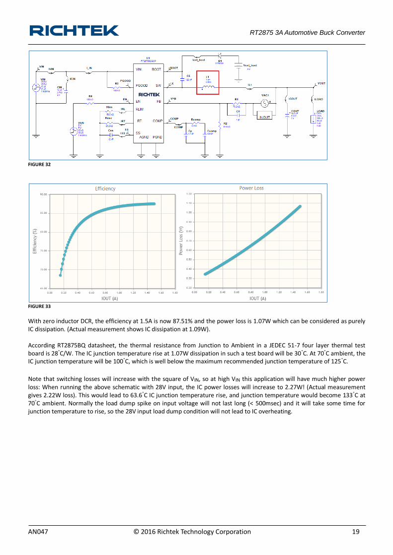
RT2875 3A Automotive Buck Converter
AN047 © 2016 Richtek Technology Corporation 19
FIGURE 32
FIGURE 33
With zero inductor DCR, the efficiency at 1.5A is now 87.51% and the power loss is 1.07W which can be considered as purely IC dissipation. (Actual measurement shows IC dissipation at 1.09W). According RT2875BQ datasheet, the thermal resistance from Junction to Ambient in a JEDEC 51-7 four layer thermal test board is 28°C/W. The IC junction temperature rise at 1.07W dissipation in such a test board will be 30°C. At 70°C ambient, the IC junction temperature will be 100°C, which is well below the maximum recommended junction temperature of 125°C.
Note that switching losses will increase with the square of VIN, so at high VIN this application will have much higher power loss: When running the above schematic with 28V input, the IC power losses will increase to 2.27W! (Actual measurement gives 2.22W loss). This would lead to 63.6°C IC junction temperature rise, and junction temperature would become 133°C at 70°C ambient. Normally the load dump spike on input voltage will not last long (< 500msec) and it will take some time for junction temperature to rise, so the 28V input load dump condition will not lead to IC overheating.
RT2875 3A Automotive Buck Converter
AN047 © 2016 Richtek Technology Corporation 20
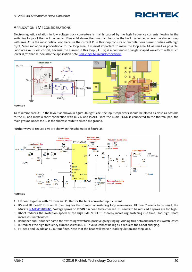
APPLICATION EMI CONSIDERATIONS
Electromagnetic radiation in low voltage buck converters is mainly caused by the high frequency currents flowing in the switching loops of the buck converter. Figure 34 shows the two main loops in the buck converter, where the shaded loop with area A1 is the most critical loop because the current I1 in this loop consists of discontinuous current pulses with high dI/dt. Since radiation is proportional to the loop area, it is most important to make the loop area A1 as small as possible. Loop area A2 is less critical, because the current in this loop (I1 + I2) is a continuous triangle shaped waveform with much lower dI/dt than I1. See also the application note Reducing EMI in buck converters.
FIGURE 34
To minimize area A1 in the layout as shown in figure 34 right side, the input capacitors should be placed as close as possible to the IC, and make a short connection with IC VIN and PGND. Since the IC die PGND is connected to the thermal pad, the main ground under the IC is the shortest route to silicon die ground. Further ways to reduce EMI are shown in the schematic of figure 35 :
FIGURE 35
1. HF bead together with C1 form an LC filter for the buck converter input current. 2. R5 and HF bead2 form an RL damping for the IC internal switching loop resonances. HF bead2 needs to be small, like
Murata BLM15PG100SN1. Voltage spikes on IC VIN pin need to be checked. R5 needs to be reduced if spikes are too high. 3. Rboot reduces the switch-on speed of the high side MOSFET, thereby increasing switching rise time. Too high Rboot
increases switch losses. 4. Rsnubber and Csnubber damp the switching waveform positive going ringing. Adding this network increases switch losses. 5. R7 reduces the high frequency current spikes in D1. R7 value cannot be big as it reduces the Cboot charging. 6. HF bead and C6 add an LC output filter. Note that the bead will worsen load regulation and step load.
RT2875 3A Automotive Buck Converter
AN047 © 2016 Richtek Technology Corporation 21
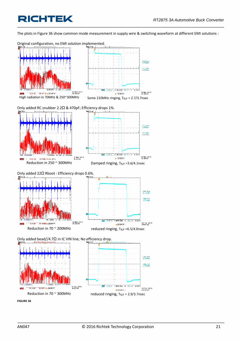
The plots in Figure 36 show common mode measurement in supply wire & switching waveform at different EMI solutions :
Original configuration, no EMI solution implemented.
High radiation in 70MHz & 250~300MHz Some 210MHz ringing, TR/F = 2.7/3.7nsec
Only added RC snubber 2.2Ω & 470pF; Efficiency drops 1%.
Reduction in 250 ~ 300MHz Damped ringing, TR/F =3.6/4.1nsec
Only added 22Ω Rboot : Efficiency drops 0.6%.
Reduction in 70 ~ 200MHz reduced ringing, TR/F =6.5/4.0nsec
Only added bead//4.7Ω in IC VIN line; No efficiency drop.
Reduction in 70 ~ 300MHz reduced ringing, TR/F = 2.9/3.7nsec
FIGURE 36
RT2875 3A Automotive Buck Converter
AN047 © 2016 Richtek Technology Corporation 22
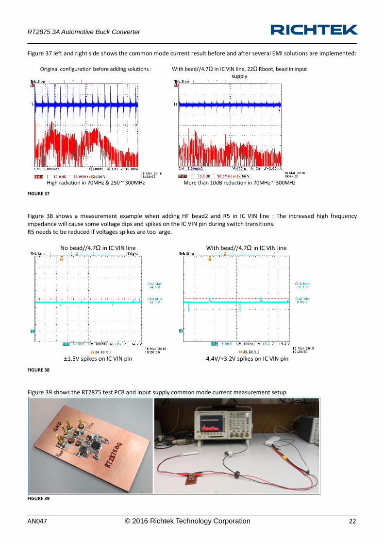
Figure 37 left and right side shows the common mode current result before and after several EMI solutions are implemented:
Original configuration before adding solutions : With bead//4.7Ω in IC VIN line, 22Ω Rboot, bead in input supply
High radiation in 70MHz & 250 ~ 300MHz More than 10dB reduction in 70MHz ~ 300MHz
FIGURE 37
Figure 38 shows a measurement example when adding HF bead2 and R5 in IC VIN line : The increased high frequency impedance will cause some voltage dips and spikes on the IC VIN pin during switch transitions. R5 needs to be reduced if voltages spikes are too large.
No bead//4.7Ω in IC VIN line With bead//4.7Ω in IC VIN line
±1.5V spikes on IC VIN pin -4.4V/+3.2V spikes on IC VIN pin
FIGURE 38
Figure 39 shows the RT2875 test PCB and input supply common mode current measurement setup.
FIGURE 39
RT2875 3A Automotive Buck Converter
AN047 © 2016 Richtek Technology Corporation 23
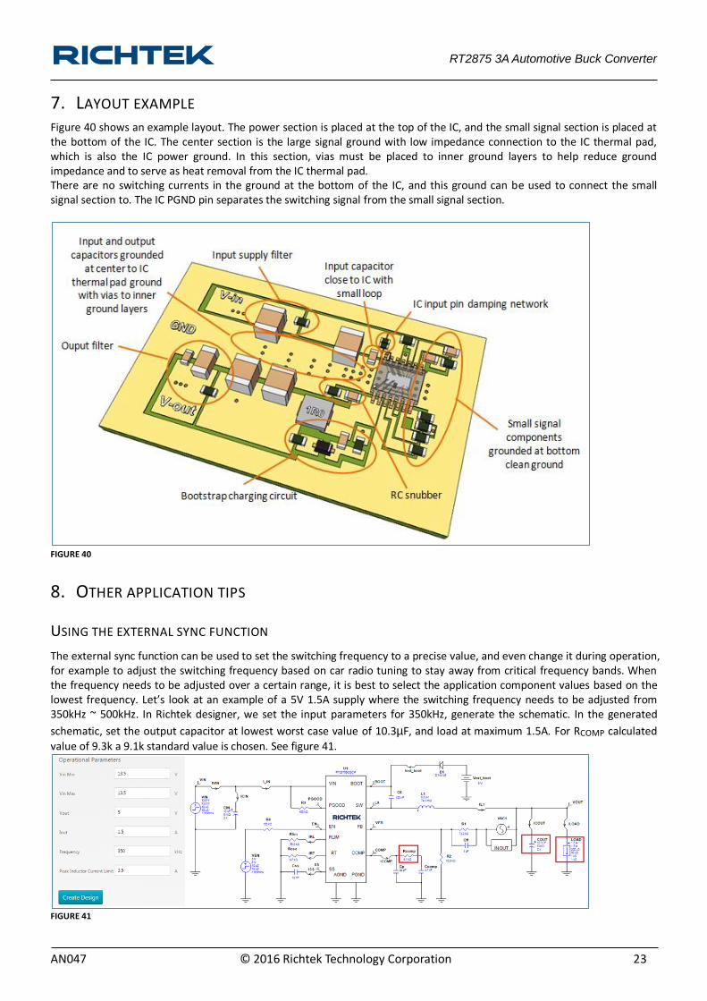
7. LAYOUT EXAMPLE Figure 40 shows an example layout. The power section is placed at the top of the IC, and the small signal section is placed at the bottom of the IC. The center section is the large signal ground with low impedance connection to the IC thermal pad, which is also the IC power ground. In this section, vias must be placed to inner ground layers to help reduce ground impedance and to serve as heat removal from the IC thermal pad. There are no switching currents in the ground at the bottom of the IC, and this ground can be used to connect the small signal section to. The IC PGND pin separates the switching signal from the small signal section.
FIGURE 40
8. OTHER APPLICATION TIPS
USING THE EXTERNAL SYNC FUNCTION
The external sync function can be used to set the switching frequency to a precise value, and even change it during operation, for example to adjust the switching frequency based on car radio tuning to stay away from critical frequency bands. When the frequency needs to be adjusted over a certain range, it is best to select the application component values based on the lowest frequency. Let’s look at an example of a 5V 1.5A supply where the switching frequency needs to be adjusted from 350kHz ~ 500kHz. In Richtek designer, we set the input parameters for 350kHz, generate the schematic. In the generated
schematic, set the output capacitor at lowest worst case value of 10.3µF, and load at maximum 1.5A. For RCOMP calculated
value of 9.3k a 9.1k standard value is chosen. See figure 41.
FIGURE 41
RT2875 3A Automotive Buck Converter
AN047 © 2016 Richtek Technology Corporation 24
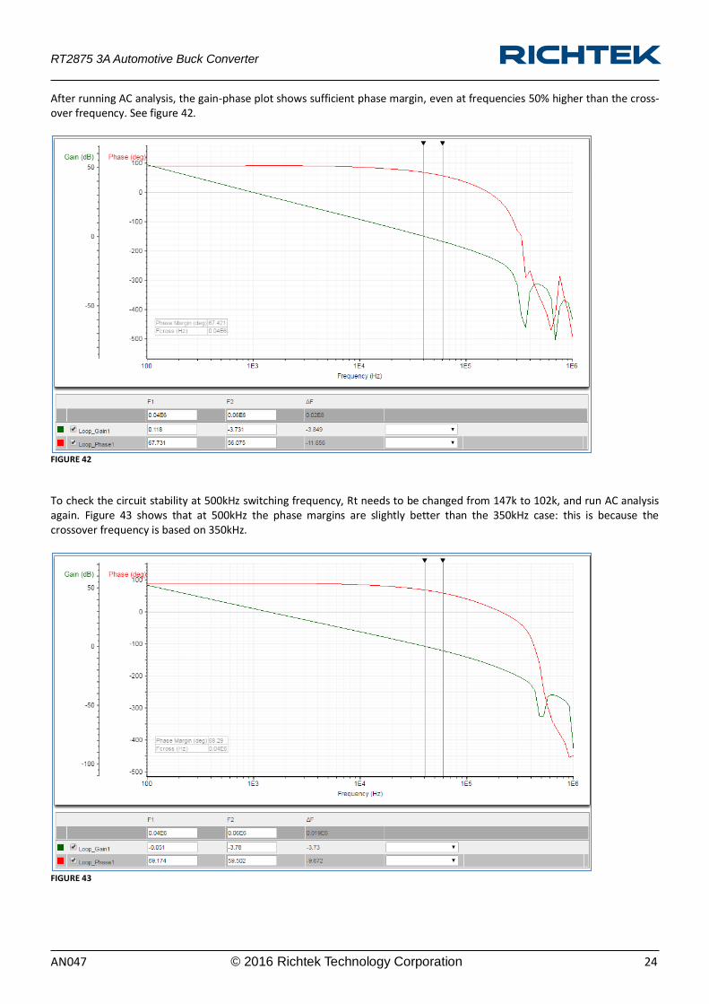
After running AC analysis, the gain-phase plot shows sufficient phase margin, even at frequencies 50% higher than the cross-over frequency. See figure 42.
FIGURE 42
To check the circuit stability at 500kHz switching frequency, Rt needs to be changed from 147k to 102k, and run AC analysis again. Figure 43 shows that at 500kHz the phase margins are slightly better than the 350kHz case: this is because the crossover frequency is based on 350kHz.
FIGURE 43

RT2875 3A Automotive Buck Converter
AN047 © 2016 Richtek Technology Corporation 25
In most systems where external sync is applied, the sync signal is generated by a micro controller (MCU). If the MCU is powered by the same Buck converter it is trying to synchronize, problems can occur during power-up, because the MCU SYNC I/O may temporary pull down the RT2875 RT/SYNC pin, and the converter won’t start or will malfunction with RT/SYNC temporary shorted to ground. To solve this problem, the circuit configuration as shown in figure 44 is recommended. The MCU SYNC I/O pin is not connected directly to the RT/SYNC pin, but via the voltage divider Rt1/Rt2. In this way, even when the MCU pin is low, the RT2875 will work at a defined frequency via Rt1 (in this case resulting in a 500kHz frequency). When the MCU SYNC pin is floating, the frequency is defined by Rt1 + Rt2 (in this case resulting in a 350kHz frequency). When the MCU SYNC pin sends out a square-wave SYNC signal, RT2875 will synchronize to this signal. It is recommended to add a capacitor Ct in parallel with Rt1. The time-constant Rt1 * Ct should be based on the lowest SYNC frequency period. Although RT2875 can also start with external SYNC signal applied, in this application we start without external sync, and use the RT2875 PGOOD signal to tell the MCU that the SYNC signal can be activated.
FIGURE 44
Figure 45 shows the converter start-up sequence with above circuit : The MCU was programmed for SYNC pin in tri-state initially; then a 350kHz 50% duty PWM command was given.
Start-up from VIN with external sync application Detailed look at the free-running to SYNC transition
FIGURE 45
From figure 45 right side it can be seen that the MCU SYNC pin is initially floating, resulting in ~347kHz switching frequency (defined by Rt1 + Rt2). When the MCU PWM command is issued, the MCU SYNC pin will first go low for around 24µsec. During this time, the RT2875 frequency goes to 500kHz (defined by Rt1). When the 350kHz SYNC pulses appear, RT2875 uses 4 cycles to measure the frequency and set the converter internal parameters for this new frequency. During this time, the converter runs at highest frequency. After that, the converter synchronizes to the new SYNC frequency. When the SYNC pin is set in tri-state again, a similar transition will occur and the converter moves back to the frequency set by the Rt1 + Rt2 resistors.
RT2875 3A Automotive Buck Converter
AN047 © 2016 Richtek Technology Corporation 26
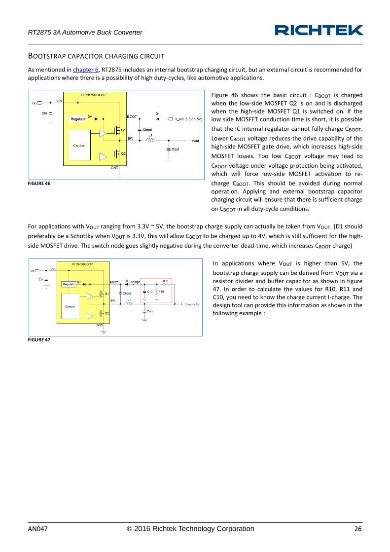
BOOTSTRAP CAPACITOR CHARGING CIRCUIT
As mentioned in chapter 6, RT2875 includes an internal bootstrap charging circuit, but an external circuit is recommended for applications where there is a possibility of high duty-cycles, like automotive applications.
FIGURE 46
Figure 46 shows the basic circuit : CBOOT is charged when the low-side MOSFET Q2 is on and is discharged when the high-side MOSFET Q1 is switched on. If the low side MOSFET conduction time is short, it is possible
that the IC internal regulator cannot fully charge CBOOT.
Lower CBOOT voltage reduces the drive capability of the high-side MOSFET gate drive, which increases high-side
MOSFET losses. Too low CBOOT voltage may lead to
CBOOT voltage under-voltage protection being activated, which will force low-side MOSFET activation to re-
charge CBOOT. This should be avoided during normal operation. Applying and external bootstrap capacitor charging circuit will ensure that there is sufficient charge
on CBOOT in all duty-cycle conditions.
For applications with VOUT ranging from 3.3V ~ 5V, the bootstrap charge supply can actually be taken from VOUT. (D1 should
preferably be a Schottky when VOUT is 3.3V, this will allow CBOOT to be charged up to 4V, which is still sufficient for the high-
side MOSFET drive. The switch node goes slightly negative during the converter dead-time, which increases CBOOT charge)
FIGURE 47
In applications where VOUT is higher than 5V, the
bootstrap charge supply can be derived from VOUT via a resistor divider and buffer capacitor as shown in figure 47. In order to calculate the values for R10, R11 and C10, you need to know the charge current I-charge. The design tool can provide this information as shown in the following example :
RT2875 3A Automotive Buck Converter
AN047 © 2016 Richtek Technology Corporation 27
We design a 6V/1.5A supply running at 1MHz frequency by entering the data as shown in figure 48 left side :
FIGURE 48
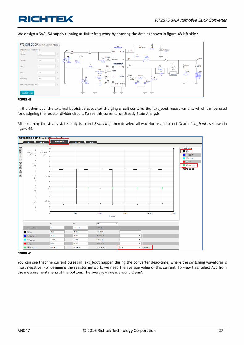
In the schematic, the external bootstrap capacitor charging circuit contains the Iext_boot measurement, which can be used for designing the resistor divider circuit. To see this current, run Steady State Analysis. After running the steady state analysis, select Switching, then deselect all waveforms and select LX and Iext_boot as shown in figure 49.
FIGURE 49
You can see that the current pulses in Iext_boot happen during the converter dead-time, where the switching waveform is most negative. For designing the resistor network, we need the average value of this current. To view this, select Avg from the measurement menu at the bottom. The average value is around 2.5mA.
RT2875 3A Automotive Buck Converter
AN047 © 2016 Richtek Technology Corporation 28
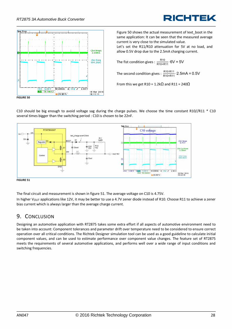
FIGURE 50
Figure 50 shows the actual measurement of Iext_boot in the same application: It can be seen that the measured average current is very close to the simulated value. Let’s set the R11/R10 attenuation for 5V at no load, and allow 0.5V drop due to the 2.5mA charging current.
The fist condition gives : R10
R10+R11∙6V = 5V
The second condition gives : R10∙R11
R10+R11∙2.5mA = 0.5V
From this we get R10 = 1.2kΩ and R11 = 240Ω
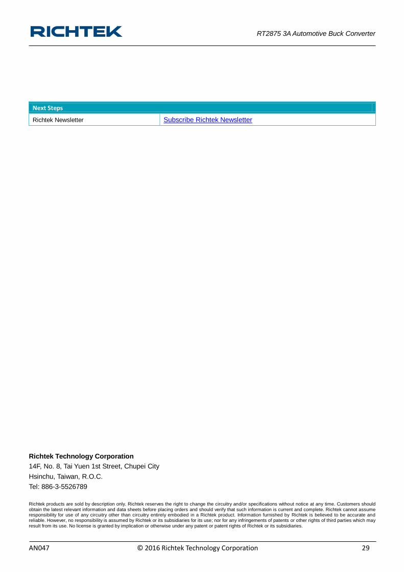
C10 should be big enough to avoid voltage sag during the charge pulses. We choose the time constant R10//R11 * C10 several times bigger than the switching period : C10 is chosen to be 22nF.
FIGURE 51
The final circuit and measurement is shown in figure 51. The average voltage on C10 is 4.75V.
In higher VOUT applications like 12V, it may be better to use a 4.7V zener diode instead of R10. Choose R11 to achieve a zener bias current which is always larger than the average charge current.
9. CONCLUSION Designing an automotive application with RT2875 takes some extra effort if all aspects of automotive environment need to be taken into account: Component tolerances and parameter drift over temperature need to be considered to ensure correct operation over all critical conditions. The Richtek Designer simulation tool can be used as a good guideline to calculate initial component values, and can be used to estimate performance over component value changes. The feature set of RT2875 meets the requirements of several automotive applications, and performs well over a wide range of input conditions and switching frequencies.
RT2875 3A Automotive Buck Converter
AN047 © 2016 Richtek Technology Corporation 29
Next Steps
Richtek Newsletter Subscribe Richtek Newsletter
Richtek Technology Corporation
14F, No. 8, Tai Yuen 1st Street, Chupei City
Hsinchu, Taiwan, R.O.C.
Tel: 886-3-5526789
Richtek products are sold by description only. Richtek reserves the right to change the circuitry and/or specifications without notice at any time. Customers should obtain the latest relevant information and data sheets before placing orders and should verify that such information is current and complete. Richtek cannot assume responsibility for use of any circuitry other than circuitry entirely embodied in a Richtek product. Information furnished by Richtek is believed to be accurate and reliable. However, no responsibility is assumed by Richtek or its subsidiaries for its use; nor for any infringements of patents or other rights of third parties which may result from its use. No license is granted by implication or otherwise under any patent or patent rights of Richtek or its subsidiaries.