rf/optical engineering - viking technology · viking technology’s engineering services, ......
TRANSCRIPT
RF/OPTICAL ENGINEERINGYOUR STRATEGIC PARTNER IN RF, OPTICAL, & MICROELECTRONIC DESIGN
2 VIKING TECHNOLOGY | RF/Optical Engineering
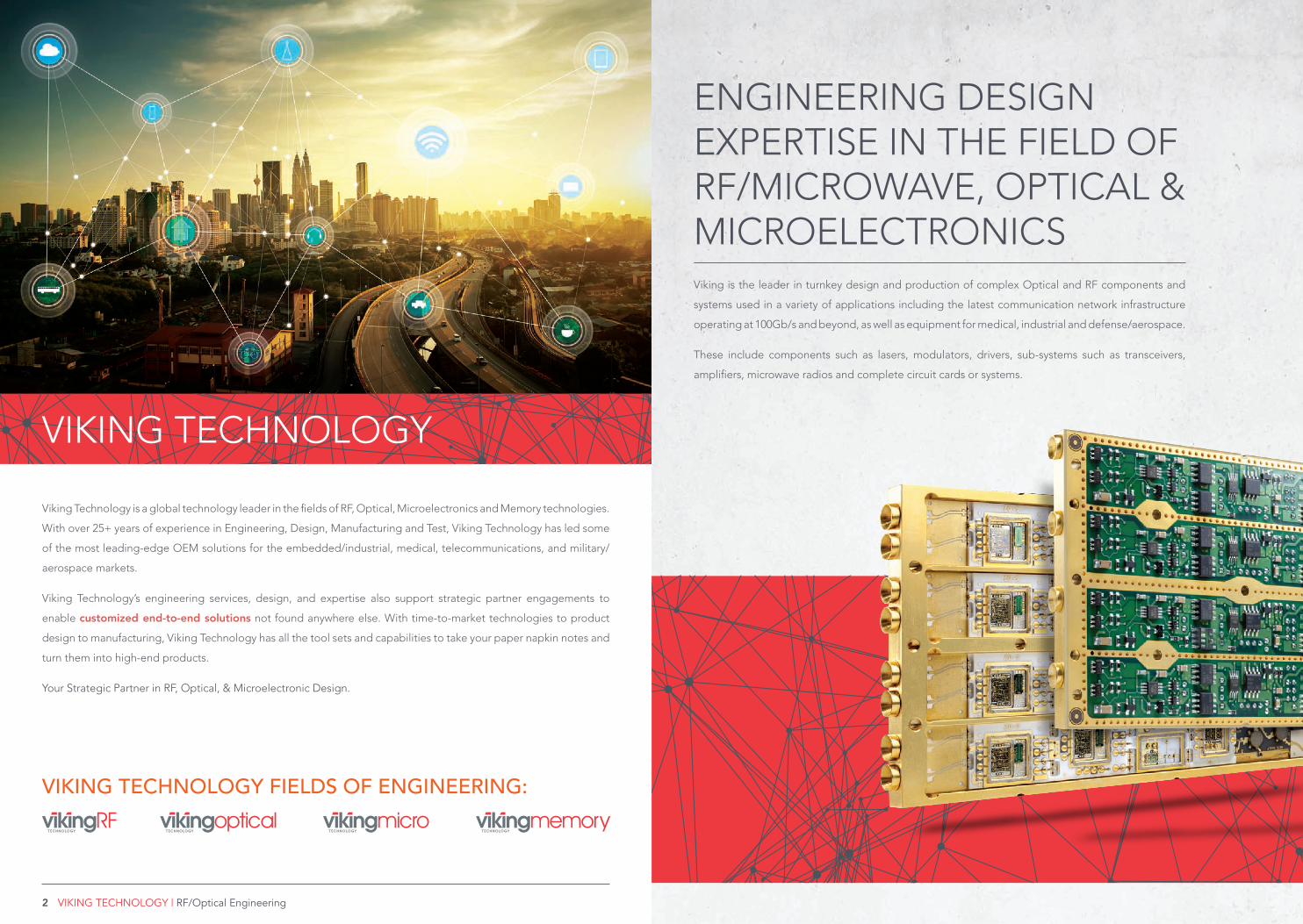
VIKING TECHNOLOGY FIELDS OF ENGINEERING:
VIKING TECHNOLOGY
Viking Technology is a global technology leader in the fields of RF, Optical, Microelectronics and Memory technologies.
With over 25+ years of experience in Engineering, Design, Manufacturing and Test, Viking Technology has led some
of the most leading-edge OEM solutions for the embedded/industrial, medical, telecommunications, and military/
aerospace markets.
Viking Technology’s engineering services, design, and expertise also support strategic partner engagements to
enable customized end-to-end solutions not found anywhere else. With time-to-market technologies to product
design to manufacturing, Viking Technology has all the tool sets and capabilities to take your paper napkin notes and
turn them into high-end products.
Your Strategic Partner in RF, Optical, & Microelectronic Design.
ENGINEERING DESIGN EXPERTISE IN THE FIELD OF RF/MICROWAVE, OPTICAL &MICROELECTRONICSViking is the leader in turnkey design and production of complex Optical and RF components and
systems used in a variety of applications including the latest communication network infrastructure
operating at 100Gb/s and beyond, as well as equipment for medical, industrial and defense/aerospace.
These include components such as lasers, modulators, drivers, sub-systems such as transceivers,
amplifiers, microwave radios and complete circuit cards or systems.
4 VIKING TECHNOLOGY | RF/Optical Engineering 5VIKING TECHNOLOGY | RF/Optical Engineering
TECHNOLOGY
Advanced microelectronic technologies – bare die packaging, wire bonding, flip-chip, optical interconnection
High-speed RF & Optical multi-chip modules (MCM)
High-speed materials & interconnections (advanced ceramics & organic laminates, build-up, flex)
Precision optical alignment & interconnection
PRODUCT DESIGN
Product design for RF, Microwave & Optical applications (analog/digital)
Computer modeling for Optical, RF/EM, Electrical, Thermal, Mechanical
Test systems development (HW/SW)
10/40/100/200Gb/s & beyond – Components, Modules, Blades
Communications, Medical, Industrial, Defense & Aerospace
MANUFACTURING
Assembly & test processes for complex RF & Opto-electronic products (Circuit cards, Modules, Components)
Advanced microelectronic & micro-optic processes (chip & wire, flip-chip, active/passive alignment, hermetic sealing)
Flexible manufacturing for early NPI prototypes
Test processes for RF/Optical
Global manufacturing
RF, Optical, Thermal interconnection design
Substrate/package design
Hermetic, non-hermetic
Package to system interconnection
Components: Drivers, Amplifiers, TRX,
Modulators, antennas, lasers, etc.
RF, OPTICAL COMPONENT DESIGN
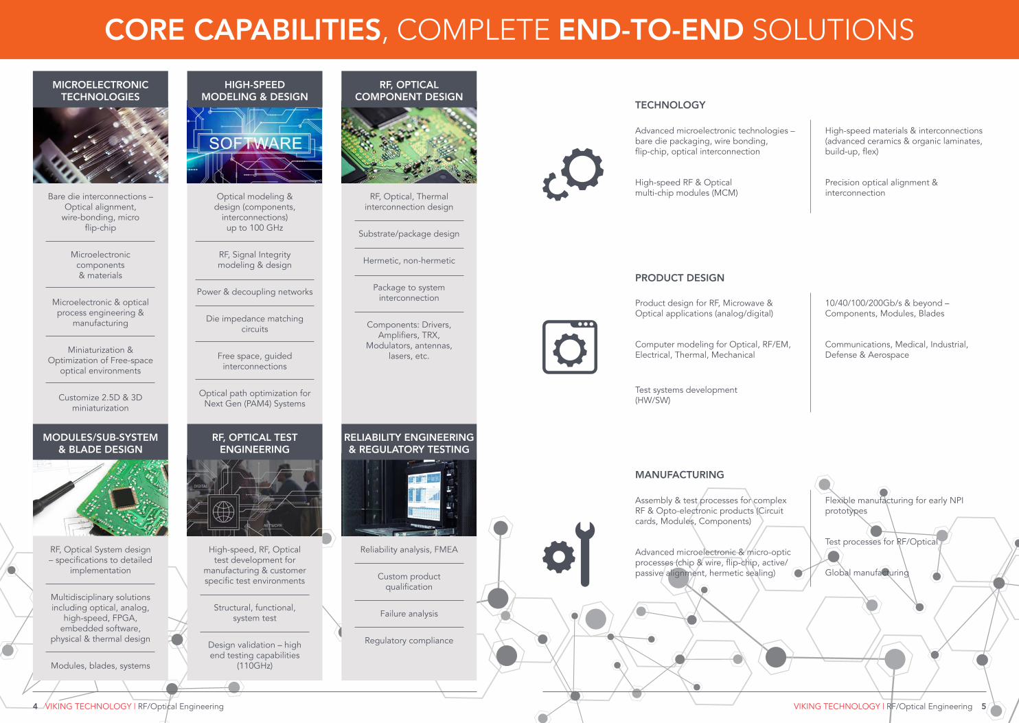
CORE CAPABILITIES, COMPLETE END-TO-END SOLUTIONS
RF, Optical System design – specifications to detailed
implementation
Multidisciplinary solutions including optical, analog,
high-speed, FPGA, embedded software,
physical & thermal design
Modules, blades, systems
High-speed, RF, Optical test development for
manufacturing & customer specific test environments
Structural, functional, system test
Design validation – high end testing capabilities
(110GHz)
Reliability analysis, FMEA
Custom product qualification
Failure analysis
Regulatory compliance
MODULES/SUB-SYSTEM & BLADE DESIGN
RF, OPTICAL TEST ENGINEERING
RELIABILITY ENGINEERING & REGULATORY TESTING
Bare die interconnections – Optical alignment,
wire-bonding, micro flip-chip
Microelectronic components & materials
Microelectronic & optical process engineering &
manufacturing
Miniaturization & Optimization of Free-space
optical environments
Customize 2.5D & 3D miniaturization
Optical modeling & design (components,
interconnections) up to 100 GHz
RF, Signal Integrity modeling & design
Power & decoupling networks
Die impedance matching circuits
Free space, guided interconnections
Optical path optimization for Next Gen (PAM4) Systems
HIGH-SPEED MODELING & DESIGN
MICROELECTRONIC TECHNOLOGIES
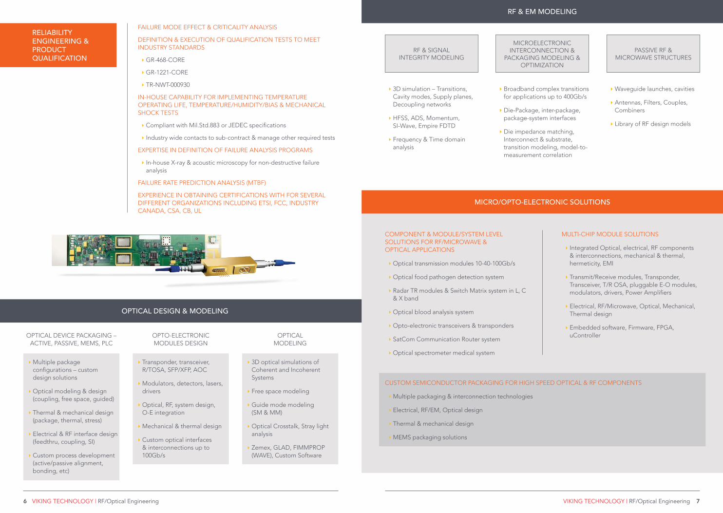
MICRO/OPTO-ELECTRONIC SOLUTIONS
RF & EM MODELING
OPTICAL DESIGN & MODELING
6 VIKING TECHNOLOGY | RF/Optical Engineering 7VIKING TECHNOLOGY | RF/Optical Engineering
FAILURE MODE EFFECT & CRITICALITY ANALYSIS
DEFINITION & EXECUTION OF QUALIFICATION TESTS TO MEET INDUSTRY STANDARDS
‣ GR-468-CORE
‣ GR-1221-CORE
‣ TR-NWT-000930
IN-HOUSE CAPABILITY FOR IMPLEMENTING TEMPERATURE OPERATING LIFE, TEMPERATURE/HUMIDITY/BIAS & MECHANICAL SHOCK TESTS
‣ Compliant with Mil.Std.883 or JEDEC specifications
‣ Industry wide contacts to sub-contract & manage other required tests
EXPERTISE IN DEFINITION OF FAILURE ANALYSIS PROGRAMS
‣ In-house X-ray & acoustic microscopy for non-destructive failure analysis
FAILURE RATE PREDICTION ANALYSIS (MTBF)
EXPERIENCE IN OBTAINING CERTIFICATIONS WITH FOR SEVERAL DIFFERENT ORGANIZATIONS INCLUDING ETSI, FCC, INDUSTRY CANADA, CSA, CB, UL
RELIABILITY ENGINEERING & PRODUCT QUALIFICATION
‣ 3D simulation – Transitions, Cavity modes, Supply planes, Decoupling networks
‣ HFSS, ADS, Momentum, SI-Wave, Empire FDTD
‣ Frequency & Time domain analysis
RF & SIGNAL INTEGRITY MODELING
‣ Broadband complex transitions for applications up to 400Gb/s
‣ Die-Package, inter-package, package-system interfaces
‣ Die impedance matching, Interconnect & substrate, transition modeling, model-to-measurement correlation
MICROELECTRONIC INTERCONNECTION &
PACKAGING MODELING & OPTIMIZATION
‣ Waveguide launches, cavities
‣ Antennas, Filters, Couples, Combiners
‣ Library of RF design models
PASSIVE RF &MICROWAVE STRUCTURES
COMPONENT & MODULE/SYSTEM LEVEL SOLUTIONS FOR RF/MICROWAVE & OPTICAL APPLICATIONS
‣ Optical transmission modules 10-40-100Gb/s
‣ Optical food pathogen detection system
‣ Radar TR modules & Switch Matrix system in L, C & X band
‣ Optical blood analysis system
‣ Opto-electronic transceivers & transponders
‣ SatCom Communication Router system
‣ Optical spectrometer medical system
MULTI-CHIP MODULE SOLUTIONS
‣ Integrated Optical, electrical, RF components & interconnections, mechanical & thermal, hermeticity, EMI
‣ Transmit/Receive modules, Transponder, Transceiver, T/R OSA, pluggable E-O modules, modulators, drivers, Power Amplifiers
‣ Electrical, RF/Microwave, Optical, Mechanical, Thermal design
‣ Embedded software, Firmware, FPGA, uController
CUSTOM SEMICONDUCTOR PACKAGING FOR HIGH SPEED OPTICAL & RF COMPONENTS
‣ Multiple packaging & interconnection technologies
‣ Electrical, RF/EM, Optical design
‣ Thermal & mechanical design
‣ MEMS packaging solutions
‣ Multiple package configurations – custom design solutions
‣ Optical modeling & design (coupling, free space, guided)
‣ Thermal & mechanical design (package, thermal, stress)
‣ Electrical & RF interface design (feedthru, coupling, SI)
‣ Custom process development (active/passive alignment, bonding, etc)
‣ Transponder, transceiver, R/TOSA, SFP/XFP, AOC
‣ Modulators, detectors, lasers, drivers
‣ Optical, RF, system design, O-E integration
‣ Mechanical & thermal design
‣ Custom optical interfaces & interconnections up to 100Gb/s
‣ 3D optical simulations of Coherent and Incoherent Systems
‣ Free space modeling
‣ Guide mode modeling (SM & MM)
‣ Optical Crosstalk, Stray light analysis
‣ Zemex, GLAD, FIMMPROP (WAVE), Custom Software
OPTICAL DEVICE PACKAGING – ACTIVE, PASSIVE, MEMS, PLC
OPTO-ELECTRONIC MODULES DESIGN
OPTICAL MODELING
MECHANICAL & THERMAL DESIGN
SYSTEM DESIGN
TEST ENGINEERING
8 VIKING TECHNOLOGY | RF/Optical Engineering 9VIKING TECHNOLOGY | RF/Optical Engineering
MECHANICAL DESIGN & MODELING
‣ Component, modules, circuit mechanical design with expertise in RF, micoelectronic & optics
‣ 3D solid modeling & design (Pro-Eng, Pro-Mechanica, SolidWorks, ACAD)
‣� Structural stress modeling (Ansys), Solder Joint reliability analysis
‣ Mechanical concept & detailed physical design, including tooling design
‣ Monte Carlo statistical tolerance analysis
‣ High density, high precision designs
THERMAL MODELING & DESIGN
‣ High power dissipation, density/heat flux designs
‣� Modeling & design from IC transistors, laser active region to system cooling
‣ Leading edge software tools in FEM & CFD analysis: Flotherm, Ansys
‣ Transient & steady state conditions
‣ Integrated solutions with high thermal conductivity materials
‣� Thermal verification know-how
‣ Radio, radar,optical
‣ E-O systems, pluggable optical solutions
‣ Indoor & outdoor applications
BROAD RANGE OF APPLICATIONS INCLUDING
‣ Requirements definition, specifications
‣ Architecture
‣ Link Budget analysis
‣ Feasibility (performance, real-estate, thermal, cost)
‣ Reliability analysis
‣ System Integration, Verification, NPI
‣ Certification Compliance (FCC, UL, CE)
SUPPORTING ALL PRODUCT DEVELOPMENT PHASES
‣ Circuit simulation & detailed design
‣ E-O integration
‣ PCB layout
‣ Physical design, Thermal, Shielding
‣ Firmware (CPLD, FPGA)
‣ Embedded Software
‣ Control loop algorithms & monitoring
COMPLETE MULTI-DISCIPLINARY SOLUTION
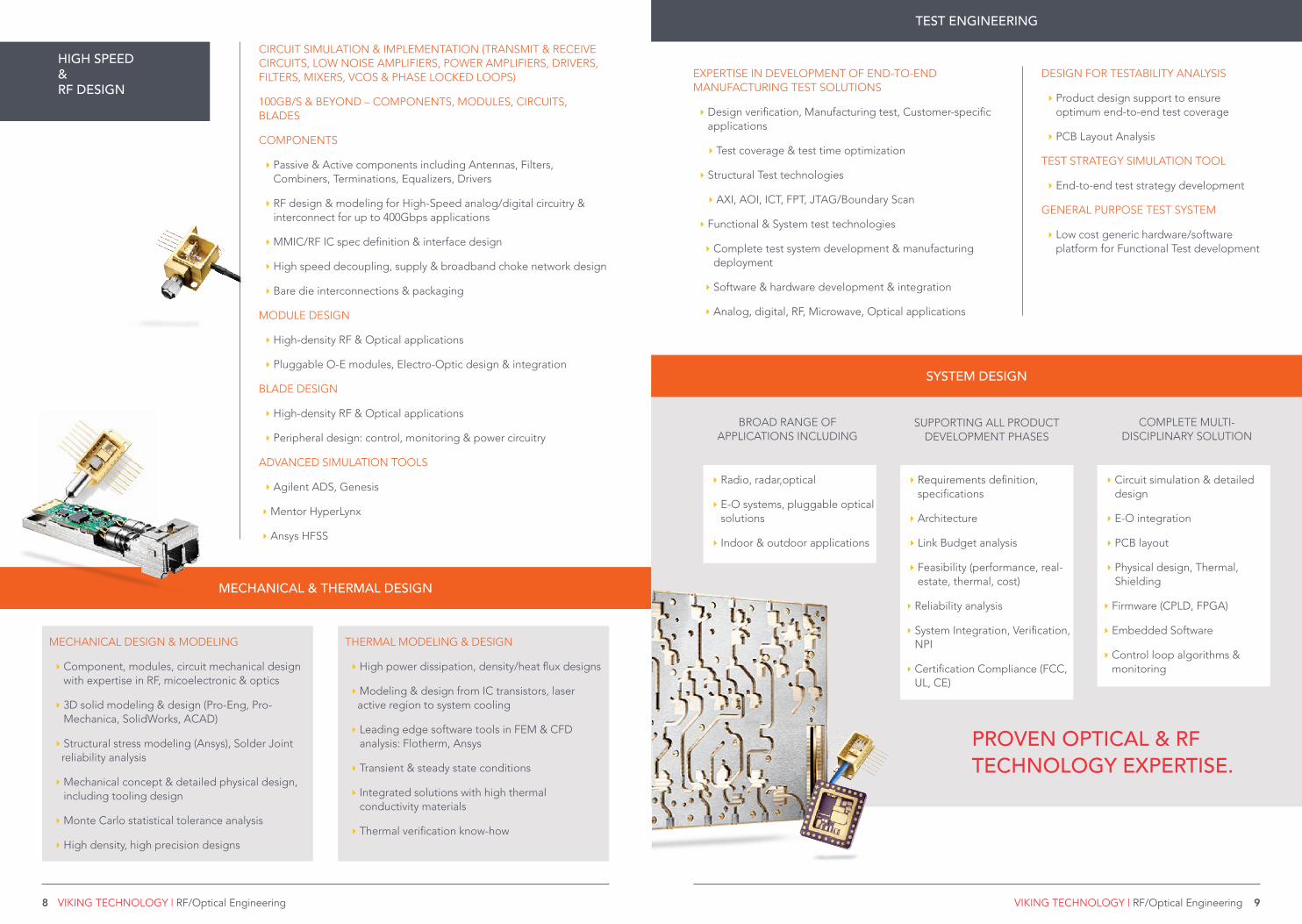
CIRCUIT SIMULATION & IMPLEMENTATION (TRANSMIT & RECEIVE CIRCUITS, LOW NOISE AMPLIFIERS, POWER AMPLIFIERS, DRIVERS, FILTERS, MIXERS, VCOS & PHASE LOCKED LOOPS)
100GB/S & BEYOND – COMPONENTS, MODULES, CIRCUITS, BLADES
COMPONENTS
‣ Passive & Active components including Antennas, Filters, Combiners, Terminations, Equalizers, Drivers
‣ RF design & modeling for High-Speed analog/digital circuitry & interconnect for up to 400Gbps applications
‣ MMIC/RF IC spec definition & interface design
‣ High speed decoupling, supply & broadband choke network design
‣ Bare die interconnections & packaging
MODULE DESIGN
‣ High-density RF & Optical applications
‣ Pluggable O-E modules, Electro-Optic design & integration
BLADE DESIGN
‣ High-density RF & Optical applications
‣ Peripheral design: control, monitoring & power circuitry
ADVANCED SIMULATION TOOLS
‣ Agilent ADS, Genesis
‣ Mentor HyperLynx
‣ Ansys HFSS
HIGH SPEED& RF DESIGN
PROVEN OPTICAL & RF TECHNOLOGY EXPERTISE.
EXPERTISE IN DEVELOPMENT OF END-TO-END MANUFACTURING TEST SOLUTIONS
‣ Design verification, Manufacturing test, Customer-specific applications
‣ Test coverage & test time optimization
‣� Structural Test technologies
‣ AXI, AOI, ICT, FPT, JTAG/Boundary Scan
‣ Functional & System test technologies
‣ Complete test system development & manufacturing deployment
‣ Software & hardware development & integration
‣ Analog, digital, RF, Microwave, Optical applications
DESIGN FOR TESTABILITY ANALYSIS
‣ Product design support to ensure optimum end-to-end test coverage
‣ PCB Layout Analysis
TEST STRATEGY SIMULATION TOOL
‣ End-to-end test strategy development
GENERAL PURPOSE TEST SYSTEM
‣ Low cost generic hardware/software platform for Functional Test development
11VIKING TECHNOLOGY | RF/Optical Engineering10 VIKING TECHNOLOGY | RF/Optical Engineering
Sanmina makes some of the most complex and innovative optical, electronic and mechanical products in the world.
Recognized as a technology leader, Sanmina provides end-to-end design, manufacturing and logistics solutions,
delivering superior quality and support to Original Equipment Manufacturers (OEMs) primarily in the communications
networks, computing and storage, medical, defense and aerospace, industrial and semiconductor, multimedia,
automotive and clean technology sectors.
Sanmina maintains a network of regional design, quick turn, New Product Introduction (NPI) facilities and repair
centers, in addition to a complete global footprint of manufacturing operations in 23 countries on six continents.
Each day, in every region of the world, Sanmina designs, manufactures ships and repairs complex, mission-critical
products. For over 30 years, customers have come to expect quality, delivery, reliability and service from Sanmina.
Together we build productive relationships based on exceptional customer satisfaction.
Viking Technology is proud to be part of the Sanmina family, with a globally recognize name in technology and
trusted partner in all of manufacturing.
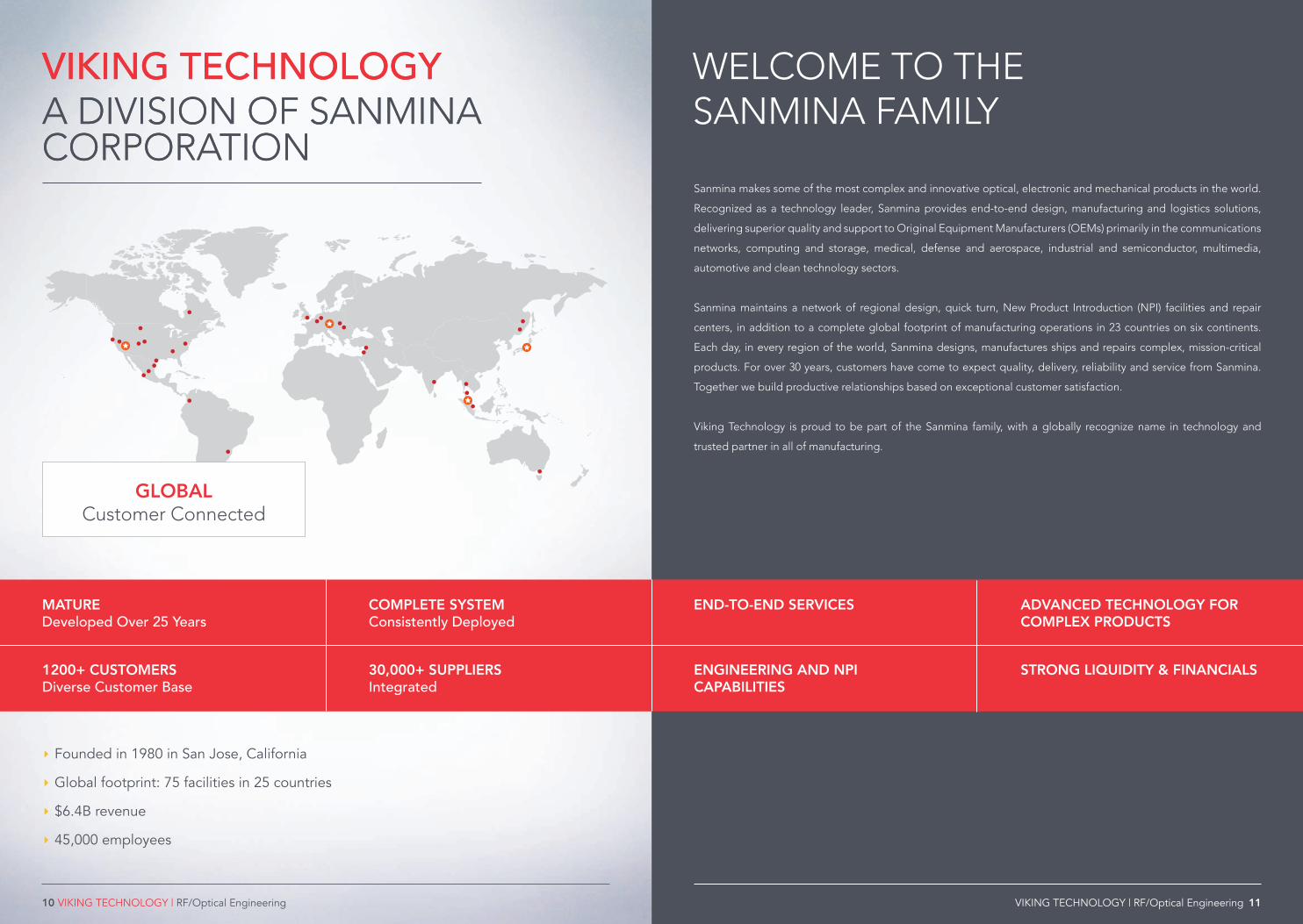
VIKING TECHNOLOGYA DIVISION OF SANMINACORPORATION
GLOBALCustomer Connected
MATUREDeveloped Over 25 Years
COMPLETE SYSTEMConsistently Deployed
1200+ CUSTOMERSDiverse Customer Base
30,000+ SUPPLIERS Integrated
‣ Founded in 1980 in San Jose, California
‣ Global footprint: 75 facilities in 25 countries
‣ $6.4B revenue
‣ 45,000 employees
END-TO-END SERVICES ADVANCED TECHNOLOGY FOR COMPLEX PRODUCTS
ENGINEERING AND NPICAPABILITIES
STRONG LIQUIDITY & FINANCIALS
VIKING TECHNOLOGYA DIVISION OF SANMINACORPORATION
WELCOME TO THE SANMINA FAMILY

Copyright © 2017 Viking Technology, all rights reserved.
R 1.01
www.vikingtechnology.com
For sales information, email us at [email protected], or visit our website for all global locations and contact information.
Global LocationsUS Headquarters Canada Office Texas Office India Office Singapore Office2950 Red Hill AvenueCosta Mesa, CA 92626Main: +1 714 913 2200Fax: +1 714 913 2202
500 March Road Ottawa, ON K2K 0J9Canada
1201 W. Crosby RoadCarrollton, TX 75006USA
A 3, Phase II, MEPZ-Special Economic ZoneNH 45, Tambaram, Chennai-600045India
No 2 Chai Chee DriveSingapore, 109840