rf design of normal conducting deflecting cavity...rf design of normal conducting deflecting cavity...
TRANSCRIPT

RF Design of Normal Conducting Deflecting Cavity
Valery Dolgashev (SLAC), Geoff Waldschmidt, Ali Nassiri
(Argonne National Laboratory, Advanced Photon Source)
48th ICFA Advanced Beam Dynamics Workshop on Future Light Sources March 1-5, 2010
SLAC National Accelerator LaboratoryMenlo Park, California

Deflecting Cavity RF Design and Analysis G. Waldschmidt 8/23/07 2
Motivation
Deflecting Cavity RF Design and Analysis G. Waldschmidt 8/23/07 3
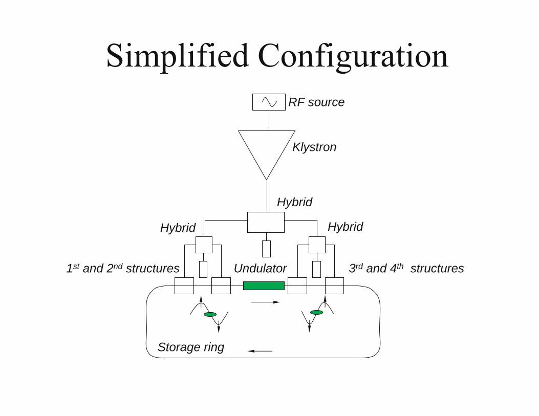
Simplified ConfigurationRF source
Hybrid
1st and 2nd structures 3rd and 4th structures
Klystron
Storage ring
Undulator
HybridHybrid

Deflecting Cavity RF Design and Analysis G. Waldschmidt 8/23/07 4
Outline• Design considerations• Thermal stability• Wakefield damping • Cavity pulsing• X-band deflector

Deflecting Cavity RF Design and Analysis G. Waldschmidt 8/23/07 5
Design requirements for APS deflecting cavity, assuming 4 cavities in the system
Frequency 2.815 GHzDeflecting Voltage 2 MV per structureAvailable power 4 MW per structureRepetition rate ~1000 Hz
The main constraints on the rf design are set by high average power loss in the cavity and heavy wakefield damping.

Deflecting Cavity RF Design and Analysis G. Waldschmidt 8/23/07 6
Design Considerations• Available power ~ 25 MW for whole system• Large aperture radius ≥ 21 mm => Low shunt
impedance• Pulsed heating < 100o C => maximum surface
magnetic field < 300 kA/m for 4 us pulse• Maximum surface electric fields < 100 MV/m• No field amplification on edges of input coupler =>
“Fat lip” coupler• Heavy loading of LOM / HOM’s• High average power operation
“Do no harm” – the set of the transverse cavities should not degrade existing operation modes of the APS ring

Deflecting Cavity RF Design and Analysis G. Waldschmidt 8/23/07 7
Evolution of the Deflecting Cavity Design
(a) 9-cell symmetric cavity with center-fed input coupler and no wakefield damping
(b) 9-cell with wakefield damping and external loads
(c) 9-cell with heavy wakefield damping and internal loads
(d) 3-cell with heavy wakefield damping and internal loads
Input coupler not shown

Deflecting Cavity RF Design and Analysis G. Waldschmidt 8/23/07 8
dampingwaveguides
input waveguide
beam axisz
y
x
3-Cell deflector fed from middle cell, 2 MeV vertical kick with 2.83 MW of input rf power
Surface electric fields for 2 MeV transverse kick. Maximum surface electric fields is 60 MV/m.
Surface magnetic fields for 2 MeV transverse kick. Maximum surface magnetic fields 240 kA/m.

Deflecting Cavity RF Design and Analysis G. Waldschmidt 8/23/07 9
3 cell deflector fed from end cell, transverse kick 2 MeV, input power 2.86 MW
Surface electric fields for 2 MeV kick, maximum fields 60.5 MV/m
Surface magnetic fields for 2 MeV kick, maximum fields 240 kA/m
232 mm
With an “end-cell coupling” the loaded Q of the next-to-working mode is reduced from 11.2·103 to 4.6·103 for critically coupled
cavity and can be reduced more for over-coupled cavity.

Deflecting Cavity RF Design and Analysis G. Waldschmidt 8/23/07 10
Deflecting Cavity with Damping Waveguides and Loads
Beam axis
HOM load in rectangular waveguide
LOM-HOM loads in ridged waveguides
Input coupler

Deflecting Cavity RF Design and Analysis G. Waldschmidt 8/23/07 11
Deflecting Cavity ParametersFrequency 2.815 GHz
Cavity Length ~23 cm
Deflecting Voltage 2 MVPeak Power 2.86 MWWorking mode Qo 12000Rt / Q 117Beam pipe aperture radius 21 mmIris radius 22 mmPhase advance per cell π
Structure length w/o beam pipes
11.17 cm
Iris thickness 18 mmDuty Factor 0.147%Kick / (Power) 1/2 1.19 MeV/MW1/2

Deflecting Cavity RF Design and Analysis G. Waldschmidt 8/23/07 12
-20
-15
-10
-5
0
5
10
15
20
-120 -80 -40 0 40 80 120
ExHy
Elec
tric
Fiel
d [M
V/m
], M
agne
tic F
ield
* Z
o [M
V/m
]
z [mm]
Transverse Electric and Magnetic Fields on Axis
Transverse electric and magnetic fields on axis vs. z for 2MeV transverse kick
EyHx

Deflecting Cavity RF Design and Analysis G. Waldschmidt 8/23/07 13
High Average Power Operation
Deflecting Cavity RF Design and Analysis G. Waldschmidt 8/23/07 14
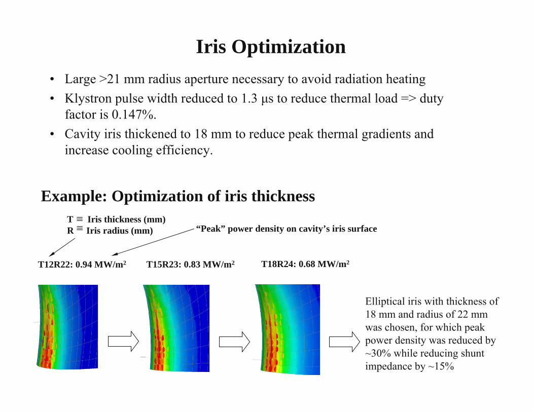
Iris Optimization• Large >21 mm radius aperture necessary to avoid radiation heating• Klystron pulse width reduced to 1.3 μs to reduce thermal load => duty
factor is 0.147%. • Cavity iris thickened to 18 mm to reduce peak thermal gradients and
increase cooling efficiency.
T12R22: 0.94 MW/m2 T15R23: 0.83 MW/m2 T18R24: 0.68 MW/m2
Elliptical iris with thickness of 18 mm and radius of 22 mm was chosen, for which peak power density was reduced by ~30% while reducing shunt impedance by ~15%
T Iris thickness (mm)R Iris radius (mm)≡≡ “Peak” power density on cavity’s iris surface
Example: Optimization of iris thickness
Deflecting Cavity RF Design and Analysis G. Waldschmidt 8/23/07 15
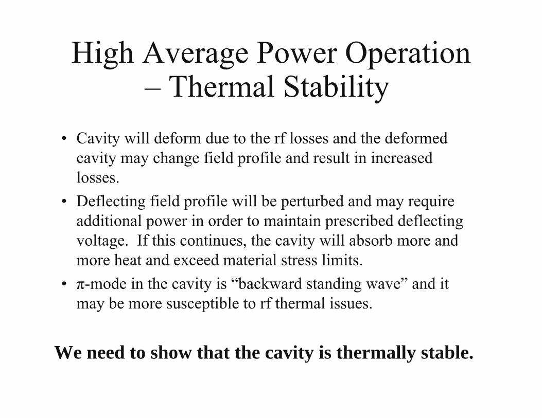
High Average Power Operation – Thermal Stability
• Cavity will deform due to the rf losses and the deformed cavity may change field profile and result in increased losses.
• Deflecting field profile will be perturbed and may require additional power in order to maintain prescribed deflecting voltage. If this continues, the cavity will absorb more and more heat and exceed material stress limits.
• π-mode in the cavity is “backward standing wave” and it may be more susceptible to rf thermal issues.
We need to show that the cavity is thermally stable.

Deflecting Cavity RF Design and Analysis G. Waldschmidt 8/23/07 16
RF / Thermal Flowchart with ANSYS
Start of rf / thermal analysis
Deformed cavity
Self-contained analysis performed entirely in ANSYS
Loop continues until power level converges
Undeformed cavity

Deflecting Cavity RF Design and Analysis G. Waldschmidt 8/23/07 17
Multi-Pass Magnetic Field DistortionMinimal field distortion after 43 iterations
Black: Original Field MagnitudeRed: Deformed Cavity Field Magnitude
Original / deformed fields are nearly identical
Deflecting Cavity RF Design and Analysis G. Waldschmidt 8/23/07 18
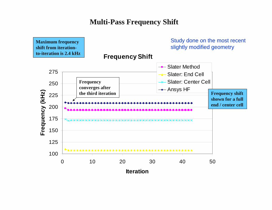
Multi-Pass Frequency Shift
Frequency Shift
100
125
150
175
200
225
250
275
0 10 20 30 40 50
Iteration
Freq
uenc
y (k
Hz)
Slater MethodSlater: End CellSlater: Center CellAnsys HF
Maximum frequency shift from iteration-to-iteration is 2.4 kHz
Frequency converges after the third iteration Frequency shift
shown for a full end / center cell
Study done on the most recent slightly modified geometry

Deflecting Cavity RF Design and Analysis G. Waldschmidt 8/23/07 19
Multi-Pass Power Loss
Power Loss
2086
2088
2090
2092
2094
2096
2098
0 10 20 30 40 50
Iteration
Pow
er
Maximum power variation from iteration-to-iteration is 10.0 W
43 iterations simulated
Study done on the most recent slightly modified geometry

Deflecting Cavity RF Design and Analysis G. Waldschmidt 8/23/07 20
Wakefield Damping

Deflecting Cavity RF Design and Analysis G. Waldschmidt 8/23/07 21
• LOM / HOM monopole and HOM dipole modes were analyzed using the frequency-domain finite-element code HFSS up to 5-6 GHz.
• MAFIA and GdFidL time-domain wakefield solvers were used to evaluate the monopole and dipole mode impedances and compare with HFSS as a verification.
• GdfidL parallel simulations calculated mode impedances > 12 GHz with λ/10 resolution in the high permittivity (εr = 30) damping material.
Low-Order-Modes/ Higher- Order-Mode analysis
3-cell structure was adopted since the heavily-loaded 9-cell cavity could not be adequately damped for beam stability.

Deflecting Cavity RF Design and Analysis G. Waldschmidt 8/23/07 22
• Mode coupling from cavity to damping waveguide was optimized to increase the damping of HOM / LOM’s and reject the operating mode (while keeping thermal issues under control)
• Monopole and horizontal dipole modes are heavily damped with a loaded Q of less than 200 for the majority of modes.
• Vertical dipole modes are not easily damped since their frequency and field configurations may be close to the operating mode.
• Ridge waveguide has been integrated into the design to improve damping of the vertical modes.
LOM/HOM Damping Considerations
Deflecting Cavity RF Design and Analysis G. Waldschmidt 8/23/07 23
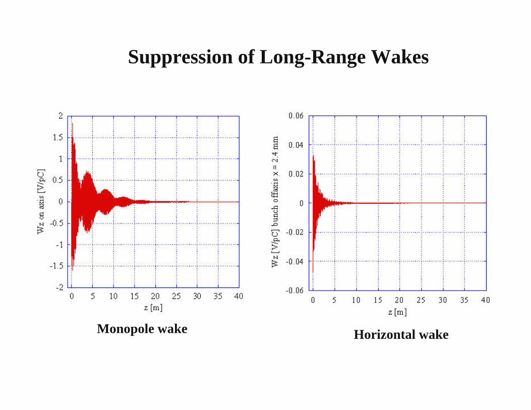
Suppression of Long-Range Wakes
x
Monopole wake Horizontal wake

Deflecting Cavity RF Design and Analysis G. Waldschmidt 8/23/07 24
Monopole Modes
2022 MHz1956 MHz
Ql ~ 130
ls P
VR2
2
=

Deflecting Cavity RF Design and Analysis G. Waldschmidt 8/23/07 25
Horizontal Dipole Modes
Ql ~ 20
2620 MHz
2663 MHz
2
2
2 ol
rrt rkP
VR o==

Deflecting Cavity RF Design and Analysis G. Waldschmidt 8/23/07 26
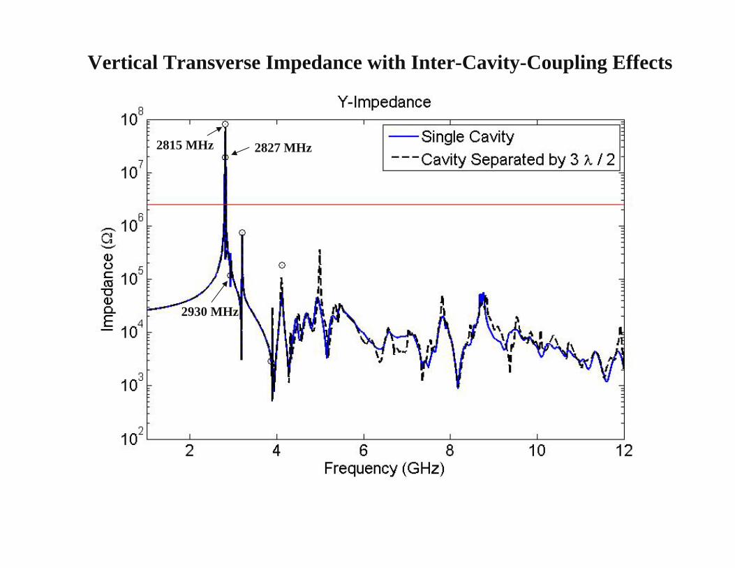
Vertical Dipole Modes
2827 MHz
2815 MHz
2827 MHz mode has a large Rt/Q and is damped minimally. It is the greatest HOM contributor to the vertical long range wake
28272815
2
2
2 ol
rrt rkP
VR o==

Deflecting Cavity RF Design and Analysis G. Waldschmidt 8/23/07 27
Z-Impedance with Inter-Cavity-Coupling Effects
o HFSS GdFidl
fp*RS < 0.8 MOhm-GHz2022 MHz
1956 MHz
Monopole Impedance

Deflecting Cavity RF Design and Analysis G. Waldschmidt 8/23/07 28
Horizontal Transverse -Impedance with Inter-Cavity-Coupling Effects
2.5 MOhm/m
o HFSS GdFidl 2620 MHz
Deflecting Cavity RF Design and Analysis G. Waldschmidt 8/23/07 29
2.5 MOhm/m
o HFSS GdFidl
2815 MHz 2827 MHz
2930 MHz
Vertical Transverse Impedance with Inter-Cavity-Coupling Effects

Deflecting Cavity RF Design and Analysis G. Waldschmidt 8/23/07 30
LOM/HOM Damper Loads – Simplified Model
Load X Center
Load X Outer
Load Y

Deflecting Cavity RF Design and Analysis G. Waldschmidt 8/23/07 31
(W)
Beam Induced Damper Load
130 mA maximum beam current, 24 singlets fill pattern generates greatest damper losses
Loss factor:Mafia: 7.802*1011
GdFidl: 7.82*1011Total losses due to monopole modes is 2.03 kW

Deflecting Cavity RF Design and Analysis G. Waldschmidt 8/23/07 32
Cavity Pulsing
• Critically matched coupler requires ~2.8 MW peak power pulsed at 1 kHz rep rate for a 2 MeV kick of the 16 mA bunch.
• Net deflecting voltage must be reduced below 13 kV for the following 86 mA bunch train (while cavity is emptying).
• Variations in cavity Q due to manufacturing or contamination creates a voltage differential• Overcouple cavity to reduce fill time constant• Reverse klystron phase to empty cavity more
quickly

Deflecting Cavity RF Design and Analysis G. Waldschmidt 8/23/07 33
Pulse Shape and Approximate Timing Diagram
16 mA enters Cav. #1 (Sector 6)
Cavity power
86 mA enters Cav. #1
Red: Ideal square inputBlack: 100 ns ramp
Timing pictorial in APS SR
Klystron power (100 ns ramp)
Duty factor 0.147%
t = 0
Vt = 0.2 MV
Ql ~ 6000 for critically coupled input coupler

Deflecting Cavity RF Design and Analysis G. Waldschmidt 8/23/07 34
Deflecting Voltage Differential for 86 mA Bunch
7.1=β
P=3.0 MW
Peak input power at cavity
1%2%3%4%5%
All cavities have Q’s ranging from Qu = 12,000 ± 600. Cavities optimally positioned based on Q’s.
Single cavity in cavity set #2 with Q 1-5% lower than nominal value (12,000)
Net difference in deflecting voltage between cavity set #1 and cavity set #2

Deflecting Cavity RF Design and Analysis G. Waldschmidt 8/23/07 35
APS Deflector Summary
• The deflecting cavity design has evolved to satisfy strict requirements in beam stability and high average power losses.
• A 3-cell standing wave structure will produce 2 MeV kick with ~2.86 MW input power for a critically coupled cavity.
• Four structures will produce a 4 MeV initial kick and a 4 MeV recovery kick.
• A single, commercially available 25 MW klystron is sufficient. • A set of two structures will occupy less then 50 cm of beam space.• Low-order and high-order modes are heavily loaded by six ridged and
four rectangular waveguides with internal loads. • Cavity power coupling has been characterized for various parameters
affecting parasitic voltage kicks to the beam.

Deflecting Cavity RF Design and Analysis G. Waldschmidt 8/23/07
X-band Deflector

Deflecting Cavity RF Design and Analysis G. Waldschmidt 8/23/07
6 cell SW 11.424 GHz deflector

Deflecting Cavity RF Design and Analysis G. Waldschmidt 8/23/07
Periodic cell of Pi standing wave deflector,0.25 MW/cell, deflecting gradient 26 MV/m
Maximum surface electric fields 105 MV/m.Maximum surface magnetic fields 410 kA/m,Pulse heating 23 deg. C for 100 ns pulse.
a = 6 mmt = 2 mm, round irisQ=7,792

Deflecting Cavity RF Design and Analysis G. Waldschmidt 8/23/07
Waveguide coupler for 6 cell SW X-band deflector,
1.5 MW of input power, deflection 2 MeV
Maximum surface electric fields ~105 MV/m.Maximum surface magnetic fields ~420 kA/m,Pulse heating 24 deg. C for 100 ns pulse.

Deflecting Cavity RF Design and Analysis G. Waldschmidt 8/23/07
Parameters of 6 cell X-band SW deflectorFrequency 11.424 GHz
Beam pipe diameter 10 mmOne cell length 13.121 mmPhase advance per cell π
One cell kick 0.34 MeV/Sqrt(0.25 MW)Structure kick (6 cells) 1 MeV/Sqrt(375 kW)Unloaded Q 7800Loaded Q 3800Maximum Electric field 53 MV/m / Sqrt(375 kW)Maximum Magnetic field 210 (kA/m) / Sqrt(375 kW)Structure length (with beam pipes) 12 cmNear mode separation 13.6 MHz

Deflecting Cavity RF Design and Analysis G. Waldschmidt 8/23/07
Summary of RF Power Considerations for X-band option
41
• SLAC 11 GHz XL-4 klystron can produce 50 MW of power at 120 Hz repetition rate and pulse length 2 μs. We expect that with some development a modified klystron can work in low power mode ~5 MW at 1 kHz repetition rate.
• A pair of 6-cell deflectors bracketing one undulator will need about 1 MW, so one such klystron is capable of powering 5 (~20 with SLED) “short x-ray pulse” stations at ~1 kHz repletion rate.
• For 1kHz operation, average power loss in 6 cell deflector would be manageable 200 W.
• With lower beam energy (say for SPEAR III) the deflectors could be driven by commercial 100 kW klystrons, like CPI’s VKX-7876E .