review silicon-based two-dimensional photonic crystal waveguides … · 2004-06-29 · 4 c. jamois...
TRANSCRIPT
Photonics and Nanostructures – Fundamentals and Applications 1 (2003) 1–13
Review
Silicon-based two-dimensional photonic crystal waveguides
C. Jamoisa,∗, R.B. Wehrspohna,b, L.C. Andreanic,C. Hermannd, O. Hessd,e, U. Göselea
a Max-Planck Institut für Mikrostrukturphysik, Weinberg 2, 06120 Halle, Germanyb Nanophotonic Materials Group, Department of Physics, University of Paderborn, Paderborn, Germany
c INFM and Dipartimento di Fisica A. Volta, Università di Pavia, Via Bassi 6, 27100 Pavia, Italyd DLR Stuttgart, Institut für Technische Physik, Theoretische Quantenelektronik, Pfaffenwaldring 38-40, 70569 Stuttgart, Germany
e Advanced Technology Institute, School of Electronics and Physical Sciences, University of Surrey, Guildford, Surrey GU2 7XH, UK
Received 14 July 2003; received in revised form 8 October 2003; accepted 10 October 2003
Abstract
A review of the properties of silicon-based two-dimensional (2D) photonic crystals is given, essentially infinite 2D photoniccrystals made from macroporous silicon and photonic crystal slabs based on silicon-on-insulator basis. We discuss the bulkphotonic crystal properties with particular attention to the light cone and its impact on the band structure. The application forwave guiding is discussed for both material systems, and compared to classical waveguides based on index-guiding. Losses ofresonant waveguide modes above the light line are discussed in detail.© 2003 Elsevier B.V. All rights reserved.
Keywords: Silicon; Photonic crystal; Waveguides
1. Introduction
In the last decades strong effort has been carriedout to investigate and control the optical properties ofmaterials, to confine light in specified areas, to pro-hibit its propagation or to allow it to propagate onlyin certain directions and at certain frequencies. Theintroduction of components based on total internalreflection for light guidance, such as optical fibers orintegrated ridge waveguides, has already enabled arevolution in the telecommunication and optical indus-try. In parallel to that, another way of controlling light
∗ Corresponding author. Tel.:+49-345-55-82-903;fax: +49-345-55-11-223.
E-mail address: [email protected] (C. Jamois).
based on Bragg diffraction has already been used inmany devices like dielectric mirrors. In 1987, the prin-ciple of dielectric mirrors leading to one-dimensional(1D) light reflection was generalized to two and threedimensions[1,2] founding a new class of materials:photonic crystals. Since then, this new field has gainedcontinuously increasing interest[3]. Photonic crystalsare materials with a periodic dielectric constant. Ifthe wavelength of light incident on the crystal is ofthe same order of magnitude as the periodicity, themultiple-scattered waves at the dielectric interfacesinterfere, leading to a band structure for photons. If thedifference between the dielectric constants of the ma-terials composing the photonic crystal is high enough,a photonic band gap—i.e. a forbidden frequency rangein a certain direction for a certain polarization—can
1569-4410/$ – see front matter © 2003 Elsevier B.V. All rights reserved.doi:10.1016/j.photonics.2003.10.001
2 C. Jamois et al. / Photonics and Nanostructures – Fundamentals and Applications 1 (2003) 1–13
occur. However, a complete photonic band gap—i.e.a forbidden frequency range in all directions for allpolarizations—can occur only in three-dimensional(3D) photonic crystals. Although these 3D photoniccrystals look very promising and have been theoreti-cally widely studied, their experimental fabrication isstill a challenge[4–8]. Therefore, 2D photonic crys-tals, which are much easier to fabricate and which stilloffer most of the interesting properties of their 3Dcounterparts, have been investigated intensively. In theideal case, 2D photonic crystals are infinitely-extendedstructures with a dielectric constant which is periodicin a plane and homogeneous in the third dimension.However, experimental structures are always finite,leading to scattering losses in the third dimension[9].More recently the concept of photonic crystal slabsconsisting of a thin 2D photonic crystal surrounded bya lower-index material has emerged and is now widelystudied, because it offers a compromise between 2Dand 3D concepts. Indeed, combining the index-guidingin the vertical direction with the presence of the pho-tonic crystal in the plane of periodicity a 3D controlof light can be achieved[10–12]. Among the severalinteresting effects in photonic crystals that can beused for a multitude of applications, such as modifica-tion of spontaneous emission[13,14] or effects basedon the particular dispersion properties like birefrin-gence[15], superprism effect and negative refraction[16–19], one of the important effects relies on the ex-istence of the band gap for wave guiding purposes. Inthis paper, some properties of 2D photonic crystals arestudied, assuming first an infinite height (Section 2)and then a finite one (Section 3). Subsequently, the in-fluence of introducing a line defect into the photoniccrystal lattice to built a waveguide is discussed, firstin the case of infinite 2D photonic crystals (Section 4)and finally in photonic crystal slabs (Section 5).
2. Infinite 2D photonic crystals
Typically, 2D photonic crystals consist of a latticeof parallel rods embedded in a substrate of differentdielectric constant. This can be either air pores in adielectric or dielectric rods in air ordered in a squareor hexagonal lattice, such that the dielectric constantis homogeneous in the direction parallel to the rodaxis—generally defined asz-direction—and periodic
in the (x, y)-plane:
ε(�r) = ε(�r + �r) (1)
where�r is any linear combination of the two unit vec-tors �a1 and�a2 of the 2D photonic crystal lattice:
�r = l�a1 + m�a2 (2)
Due to the periodicity, the eigenfunctions of thesystem can be written in the form of Bloch states,in analogy to solid state physics. In the case that themagnetic field�H is used as the variable this reads:
�Hn,�k(�r) = ei�k·�r · �u
n,�k(�r) (3)
wheren is the frequency band index,�k the wave vec-tor, and the function�u
n,�k has the periodicity of thephotonic crystal:
�un,�k(�r) = �u
n,�k(�r + �r) (4)
If the materials constituting the photonic crystal areassumed to be linear, isotropic, non-magnetic and freeof charges, the following wave equation is obtainedby combining Maxwell’s equations:
�∇ ×(
1
ε(�r)�∇ × �H(�r)
)= ω2
c2�H(�r) (5)
with
�∇ · �H(�r) = 0 (6)
This is an eigenvalue problem where the eigenvec-tors �H(�r) are called harmonic modes, and the eigenval-ues(ω/c)2 are proportional to the squared frequencyof these modes,c being the speed of light.
By solving the masterEq. (5) for k-vectors alongthe irreducible Brillouin zone of the photonic crystal,the band structure of the photonic crystal is obtained.Because the (x, y)-plane of periodicity of the 2D pho-tonic crystal is a mirror plane of the system, the polar-izations decouple, i.e. the modes can be separated intotransverse-electric (TE) modes having onlyHz, Ex andEy as non-zero components, and transverse-magnetic(TM) modes with the only non-zero componentsEz,Hx and Hy. Since TE (resp. TM) modes have theirmagnetic (resp. electric) field oriented along the poreaxis, they are often also called H (resp. E) modes.The band structures for TE and TM polarizations areusually completely different, because the electric field(resp. magnetic field) for TE and TM polarizations is
C. Jamois et al. / Photonics and Nanostructures – Fundamentals and Applications 1 (2003) 1–13 3
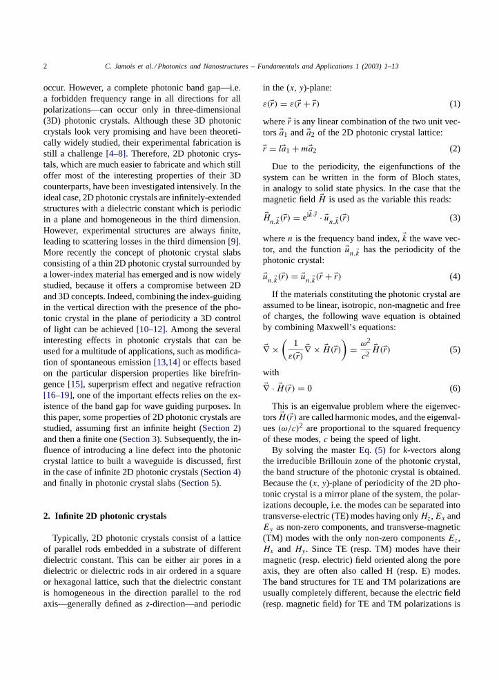
oriented in different directions relatively to the dielec-tric interfaces within the photonic crystal. In particu-lar, band gaps can exist for one polarization and notfor the other, or the position of the band gaps can bevery different. It has turned out that, while for sys-tems consisting of dielectric cylinders in air a completeband gap, i.e. a band gap for both polarizations, can beobtained only in a honeycomb lattice, the hexagonallattice of air holes in dielectric opens up a complete2D photonic band gap for a dielectric contrastn2/n1larger than 2.6[3,20].
Fig. 1 gives an example of a band structure in thecase of a hexagonal lattice of air pores in silicon witha relative radiusr/a of 0.43, wherea is the latticeconstant of the photonic crystal. The band structurecalculation was performed using the MIT package, ablock-iterative frequency-domain code[21] with a gridof 64 points per lattice constant yielding good conver-gence of the results. For this relative radius value, alarge TE band gap exists from 0.275 to 0.460 in nor-malized frequencyωa/2πc and a smaller TM bandgap from 0.385 to 0.405 that overlaps with the TEband gap, leading to a complete 2D band gap in thisfrequency range. The variation of the photonic bandgap position with relative pore radius—the so-calledgap map—for a hexagonal lattice of air pores in sil-
Fig. 1. (a) 2D hexagonal lattice and (b) its first Brillouin zone withthe irreducible Brillouin zone delimited by the three high-symmetrypoints�, M and K. (c) Band structure for a hexagonal array of airpores in silicon (ε = 11.6, r/a = 0.43) along thek-path�–M–K–�
for TE (red lines) and TM (blue lines) polarizations. The lightgrey region highlights the TE band gap and the dark grey regionthe TM (resp. complete) band gap (MIT package calculation).
Fig. 2. 2D gap map (normalized frequencyωa/2πc vs. relativepore radiusr/a) for a hexagonal lattice of air holes in silicon(ε = 11.6). The position of the largest gap-midgap ratio is indicated(MIT package calculation).
icon is shown inFig. 2. In this system, the completeband gap exists only for a relative radius larger than0.4, the largest gap–midgap ratio—ratio between bandgap width and midgap frequency—being 16.3% for apore radiusr/a = 0.478. However, such very largerelative radius values are quite difficult to achieve ex-perimentally. Therefore, most of the work based onthe existence of a band gap in 2D photonic crystalshas focussed on the TE band gap only, which is stillquite large for smaller radii, e.g. atr/a = 0.366 thegap–midgap ratio for TE modes is as large as 42.5%.
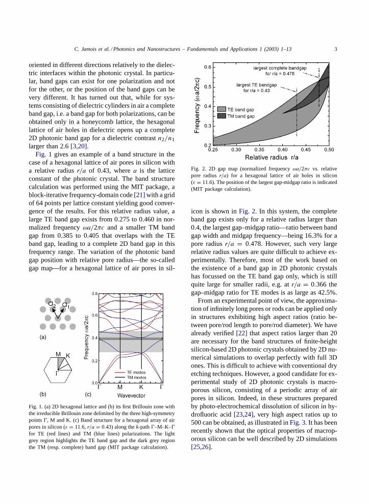
From an experimental point of view, the approxima-tion of infinitely long pores or rods can be applied onlyin structures exhibiting high aspect ratios (ratio be-tween pore/rod length to pore/rod diameter). We havealready verified[22] that aspect ratios larger than 20are necessary for the band structures of finite-heightsilicon-based 2D photonic crystals obtained by 2D nu-merical simulations to overlap perfectly with full 3Dones. This is difficult to achieve with conventional dryetching techniques. However, a good candidate for ex-perimental study of 2D photonic crystals is macro-porous silicon, consisting of a periodic array of airpores in silicon. Indeed, in these structures preparedby photo-electrochemical dissolution of silicon in hy-drofluoric acid[23,24], very high aspect ratios up to500 can be obtained, as illustrated inFig. 3. It has beenrecently shown that the optical properties of macrop-orous silicon can be well described by 2D simulations[25,26].
4 C. Jamois et al. / Photonics and Nanostructures – Fundamentals and Applications 1 (2003) 1–13
Fig. 3. SEM image of a two-dimensional hexagonal lattice of airpores in silicon with a lattice constant of 1.5�m. The pore depthis around 100�m. The bevelled etched part in front reveals thehigh uniformity of the structure from the top down to the bottomof the pores (courtesy of A. Birner, MPI Halle).
Fig. 4ashows the reflectivity of TE-polarized lightincident on a photonic crystal consisting of macrop-orous silicon in the�–M direction. The photonic crys-tal has a hexagonal lattice of air pores with a relativeradiusr/a of 0.366, and a lattice constant of 700 nm.The reflection was measured using a Fourier transfor-
Fig. 4. (a) Reflectivity of TE-polarized light incident onto a 2Dphotonic crystal made of a hexagonal lattice of air pores in siliconwith a relative radiusr/a of 0.366 and a lattice constant of 700 nm.The light beam is parallel to the plane of periodicity of thecrystal in the�–M direction (courtesy of S. Schweizer (sample)and S. Richter (measurement), MPI Halle). (b) Correspondingband structure for TE-polarization (MIT package calculation). Themodes are sorted as laterally even (blue) or laterally odd (red)modes. The regions where no odd mode exists are highlighted ingrey and correspond to the high-reflectivity regions.
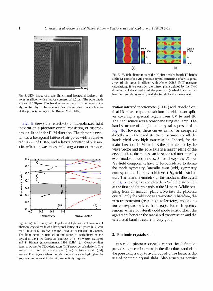
Fig. 5.Hz-field distribution of the (a) first and (b) fourth TE bandsat the M-point for a 2D photonic crystal consisting of a hexagonalarray of air pores in silicon withr/a = 0.366 (MIT packagecalculation). If we consider the mirror plane defined by the�-Mdirection and the direction of the pore axis (dashed line) the firstband has an odd symmetry and the fourth band an even one.
mation infrared spectrometer (FTIR) with attached op-tical IR microscope and calcium fluoride beam split-ter covering a spectral region from UV to mid IR.The light source was a broadband tungsten lamp. Theband structure of the photonic crystal is presented inFig. 4b. However, these curves cannot be compareddirectly with the band structure, because not all thebands yield very high transmission. Indeed, for themain directions�–M and�–K the plane defined by thewave vector and the pore axis is a mirror plane of thecrystal. Thus, the modes can be separated into laterallyeven modes or odd modes. Since always theE‖- orH⊥-field components have to be considered to definethe mode symmetry, laterally even (odd) symmetrycorresponds to laterally odd (even)Hz-field distribu-tion. The lateral symmetry of the modes is illustratedin Fig. 5, taking as examples theHz-field distributionof the first and fourth bands at the M-point. While cou-pling from an incident plane-wave into the photoniccrystal, only the odd modes are excited. Therefore, thezero-transmission (resp. high reflectivity) regions donot correspond only to band gaps, but to frequencyregions where no laterally odd mode exists. Thus, theagreement between the measured transmission and thecalculated band structure is very good.
3. Photonic crystals slabs
Since 2D photonic crystals cannot, by definition,provide light confinement in the direction parallel tothe pore axis, a way to avoid out-of-plane losses is theuse of photonic crystal slabs. Slab structures consist
C. Jamois et al. / Photonics and Nanostructures – Fundamentals and Applications 1 (2003) 1–13 5
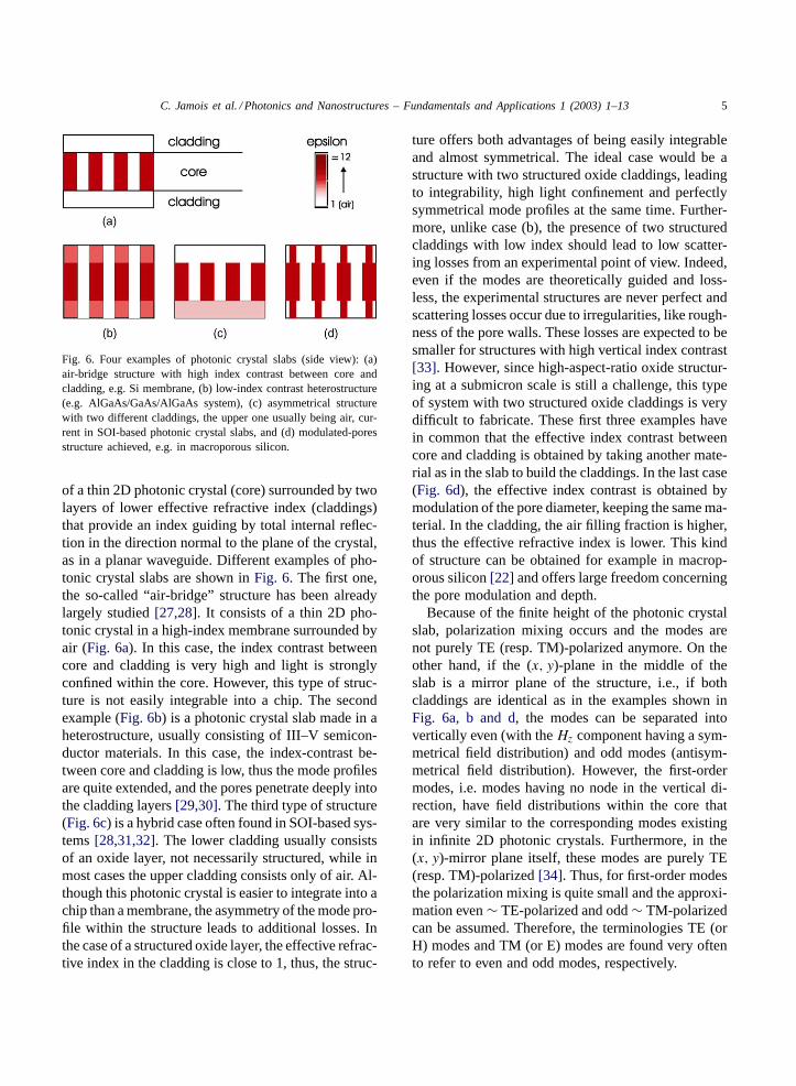
Fig. 6. Four examples of photonic crystal slabs (side view): (a)air-bridge structure with high index contrast between core andcladding, e.g. Si membrane, (b) low-index contrast heterostructure(e.g. AlGaAs/GaAs/AlGaAs system), (c) asymmetrical structurewith two different claddings, the upper one usually being air, cur-rent in SOI-based photonic crystal slabs, and (d) modulated-poresstructure achieved, e.g. in macroporous silicon.
of a thin 2D photonic crystal (core) surrounded by twolayers of lower effective refractive index (claddings)that provide an index guiding by total internal reflec-tion in the direction normal to the plane of the crystal,as in a planar waveguide. Different examples of pho-tonic crystal slabs are shown inFig. 6. The first one,the so-called “air-bridge” structure has been alreadylargely studied[27,28]. It consists of a thin 2D pho-tonic crystal in a high-index membrane surrounded byair (Fig. 6a). In this case, the index contrast betweencore and cladding is very high and light is stronglyconfined within the core. However, this type of struc-ture is not easily integrable into a chip. The secondexample (Fig. 6b) is a photonic crystal slab made in aheterostructure, usually consisting of III–V semicon-ductor materials. In this case, the index-contrast be-tween core and cladding is low, thus the mode profilesare quite extended, and the pores penetrate deeply intothe cladding layers[29,30]. The third type of structure(Fig. 6c) is a hybrid case often found in SOI-based sys-tems[28,31,32]. The lower cladding usually consistsof an oxide layer, not necessarily structured, while inmost cases the upper cladding consists only of air. Al-though this photonic crystal is easier to integrate into achip than a membrane, the asymmetry of the mode pro-file within the structure leads to additional losses. Inthe case of a structured oxide layer, the effective refrac-tive index in the cladding is close to 1, thus, the struc-
ture offers both advantages of being easily integrableand almost symmetrical. The ideal case would be astructure with two structured oxide claddings, leadingto integrability, high light confinement and perfectlysymmetrical mode profiles at the same time. Further-more, unlike case (b), the presence of two structuredcladdings with low index should lead to low scatter-ing losses from an experimental point of view. Indeed,even if the modes are theoretically guided and loss-less, the experimental structures are never perfect andscattering losses occur due to irregularities, like rough-ness of the pore walls. These losses are expected to besmaller for structures with high vertical index contrast[33]. However, since high-aspect-ratio oxide structur-ing at a submicron scale is still a challenge, this typeof system with two structured oxide claddings is verydifficult to fabricate. These first three examples havein common that the effective index contrast betweencore and cladding is obtained by taking another mate-rial as in the slab to build the claddings. In the last case(Fig. 6d), the effective index contrast is obtained bymodulation of the pore diameter, keeping the same ma-terial. In the cladding, the air filling fraction is higher,thus the effective refractive index is lower. This kindof structure can be obtained for example in macrop-orous silicon[22] and offers large freedom concerningthe pore modulation and depth.
Because of the finite height of the photonic crystalslab, polarization mixing occurs and the modes arenot purely TE (resp. TM)-polarized anymore. On theother hand, if the (x, y)-plane in the middle of theslab is a mirror plane of the structure, i.e., if bothcladdings are identical as in the examples shown inFig. 6a, b and d, the modes can be separated intovertically even (with theHz component having a sym-metrical field distribution) and odd modes (antisym-metrical field distribution). However, the first-ordermodes, i.e. modes having no node in the vertical di-rection, have field distributions within the core thatare very similar to the corresponding modes existingin infinite 2D photonic crystals. Furthermore, in the(x, y)-mirror plane itself, these modes are purely TE(resp. TM)-polarized[34]. Thus, for first-order modesthe polarization mixing is quite small and the approxi-mation even∼ TE-polarized and odd∼ TM-polarizedcan be assumed. Therefore, the terminologies TE (orH) modes and TM (or E) modes are found very oftento refer to even and odd modes, respectively.
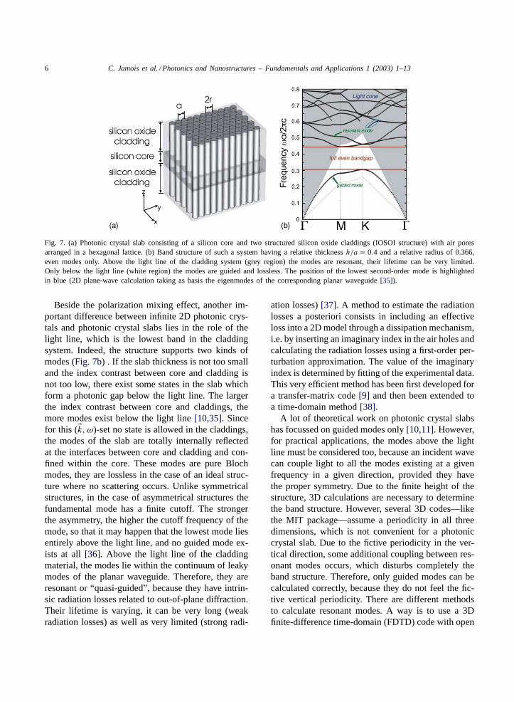
6 C. Jamois et al. / Photonics and Nanostructures – Fundamentals and Applications 1 (2003) 1–13
Fig. 7. (a) Photonic crystal slab consisting of a silicon core and two structured silicon oxide claddings (IOSOI structure) with air poresarranged in a hexagonal lattice. (b) Band structure of such a system having a relative thicknessh/a = 0.4 and a relative radius of 0.366,even modes only. Above the light line of the cladding system (grey region) the modes are resonant, their lifetime can be very limited.Only below the light line (white region) the modes are guided and lossless. The position of the lowest second-order mode is highlightedin blue (2D plane-wave calculation taking as basis the eigenmodes of the corresponding planar waveguide[35]).
Beside the polarization mixing effect, another im-portant difference between infinite 2D photonic crys-tals and photonic crystal slabs lies in the role of thelight line, which is the lowest band in the claddingsystem. Indeed, the structure supports two kinds ofmodes (Fig. 7b) . If the slab thickness is not too smalland the index contrast between core and cladding isnot too low, there exist some states in the slab whichform a photonic gap below the light line. The largerthe index contrast between core and claddings, themore modes exist below the light line[10,35]. Sincefor this (�k, ω)-set no state is allowed in the claddings,the modes of the slab are totally internally reflectedat the interfaces between core and cladding and con-fined within the core. These modes are pure Blochmodes, they are lossless in the case of an ideal struc-ture where no scattering occurs. Unlike symmetricalstructures, in the case of asymmetrical structures thefundamental mode has a finite cutoff. The strongerthe asymmetry, the higher the cutoff frequency of themode, so that it may happen that the lowest mode liesentirely above the light line, and no guided mode ex-ists at all [36]. Above the light line of the claddingmaterial, the modes lie within the continuum of leakymodes of the planar waveguide. Therefore, they areresonant or “quasi-guided”, because they have intrin-sic radiation losses related to out-of-plane diffraction.Their lifetime is varying, it can be very long (weakradiation losses) as well as very limited (strong radi-
ation losses)[37]. A method to estimate the radiationlosses a posteriori consists in including an effectiveloss into a 2D model through a dissipation mechanism,i.e. by inserting an imaginary index in the air holes andcalculating the radiation losses using a first-order per-turbation approximation. The value of the imaginaryindex is determined by fitting of the experimental data.This very efficient method has been first developed fora transfer-matrix code[9] and then been extended toa time-domain method[38].
A lot of theoretical work on photonic crystal slabshas focussed on guided modes only[10,11]. However,for practical applications, the modes above the lightline must be considered too, because an incident wavecan couple light to all the modes existing at a givenfrequency in a given direction, provided they havethe proper symmetry. Due to the finite height of thestructure, 3D calculations are necessary to determinethe band structure. However, several 3D codes—likethe MIT package—assume a periodicity in all threedimensions, which is not convenient for a photoniccrystal slab. Due to the fictive periodicity in the ver-tical direction, some additional coupling between res-onant modes occurs, which disturbs completely theband structure. Therefore, only guided modes can becalculated correctly, because they do not feel the fic-tive vertical periodicity. There are different methodsto calculate resonant modes. A way is to use a 3Dfinite-difference time-domain (FDTD) code with open
C. Jamois et al. / Photonics and Nanostructures – Fundamentals and Applications 1 (2003) 1–13 7
boundary conditions on the top and the bottom of thestructure[39,37]. It is also possible to perform 2Dplane-wave calculations taking as a basis the eigen-modes of a planar waveguide where each layer has thesame effective refractive index as the photonic crystalslab structure[35]. This is the method used inFig. 7.
If the slab thickness is increased, the cutoff fre-quency of the higher-order modes decreases, exactly asin a planar waveguide. For too thick slabs, higher-ordermodes can exist within the first-order band gap of thephotonic crystal slab. Thus, if these modes happen tohave the right symmetry properties to be excited byan external light beam, they can limit the band gap oreven destroy it completely. Reducing the vertical indexcontrast�n, the cutoff frequency of the higher-ordermodes increases. A first guess to determine the cutofffrequency of the lowest second-order mode is to usethe planar waveguide approximation. In this very sim-ple approximation, we calculate the cutoff frequencyof the second mode in a planar waveguide where eachlayer has the same effective refractive index as thephotonic crystal slab, using the relation
h
λ0= 1
2√
n22 − n2
1
(7)
whereh is the thickness of the core,λ0 the cutoff wave-length,n1 andn2 the effective indices in the claddingsand in the core, respectively, and for a photonic crys-tal:h
λ0= h
a
a
λ0(8)
with h/a the relative thickness of the slab anda/λ0 =ωa/2πc the normalized cutoff frequency of the mode.There are different methods to determine the effectiverefractive index of a photonic crystal. We choose hereto consider the light lines of the 2D systems corre-sponding to core and claddings and take the inverse oftheir tangent at the�-point. For example, for a pho-tonic crystal slab consisting of a silicon slab (ε = 11.6)and two structured silicon oxide claddings (ε = 2.1)with a relative radius of 0.366, the effective refractiveindices are 2.57 in the core and 1.25 in the claddings.This leads for a relative silicon thickness of 0.4 toa cutoff frequency of 0.56 for the first second-ordermode. Such a system as well as the correspondingband structure have already been presented inFig. 7.It can be seen on the band structure that the lowest
second-order mode has a cutoff frequency around 0.57that is very close to the value calculated using theplanar waveguide approximation. Therefore, this verysimple method gives already a good guess of the cutofffrequency of higher-order modes in photonic crystalslabs.
4. Waveguides in infinite 2D photonic crystals
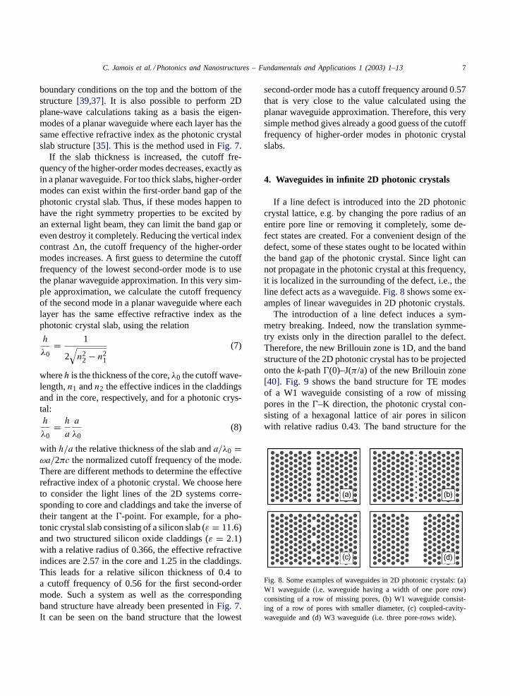
If a line defect is introduced into the 2D photoniccrystal lattice, e.g. by changing the pore radius of anentire pore line or removing it completely, some de-fect states are created. For a convenient design of thedefect, some of these states ought to be located withinthe band gap of the photonic crystal. Since light cannot propagate in the photonic crystal at this frequency,it is localized in the surrounding of the defect, i.e., theline defect acts as a waveguide.Fig. 8shows some ex-amples of linear waveguides in 2D photonic crystals.
The introduction of a line defect induces a sym-metry breaking. Indeed, now the translation symme-try exists only in the direction parallel to the defect.Therefore, the new Brillouin zone is 1D, and the bandstructure of the 2D photonic crystal has to be projectedonto thek-path�(0)–J(π/a) of the new Brillouin zone[40]. Fig. 9 shows the band structure for TE modesof a W1 waveguide consisting of a row of missingpores in the�–K direction, the photonic crystal con-sisting of a hexagonal lattice of air pores in siliconwith relative radius 0.43. The band structure for the
Fig. 8. Some examples of waveguides in 2D photonic crystals: (a)W1 waveguide (i.e. waveguide having a width of one pore row)consisting of a row of missing pores, (b) W1 waveguide consist-ing of a row of pores with smaller diameter, (c) coupled-cavity-waveguide and (d) W3 waveguide (i.e. three pore-rows wide).
8 C. Jamois et al. / Photonics and Nanostructures – Fundamentals and Applications 1 (2003) 1–13
Fig. 9. (a) SEM picture and (b) band structure for the TE polar-ization of a linear waveguide in a 2D photonic crystal. The pho-tonic crystal consists of a hexagonal lattice of air pores in siliconwith lattice constant 1.5�m and relative radius 0.43. The lineardefect is made of a row of missing pores in the�–K direction.The defect modes are sorted into index-guided (dashed lines) andphotonic-band-gap guided modes (solid lines) as well as into lat-erally odd (red lines) and even modes (blue lines) (MIT packagecalculation).
corresponding bulk photonic crystal has already beenpresented inFig. 1. The grey regions inFig. 9 corre-spond to the continuum of projected bands of the bulkphotonic crystal. Comparison withFig. 1 shows thatthere is a TE band gap in the frequency region from0.275 to 0.460 where several defect states are located.However, not all of these defect states are guided dueto the presence of the photonic band gap. Indeed, insuch a structure two guiding mechanisms coexist. Thefirst one is based on the existence of the photonic bandgap and the second one is classical index guiding dueto the effective index contrast between the waveguideand its surrounding.
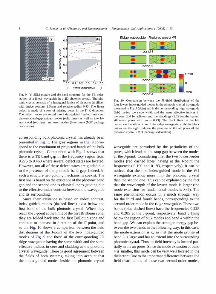
Since their existence is based on index contrast,index-guided modes (dashed lines) exist below thefirst band of the bulk photonic crystal. When theyreach the J-point at the limit of the first Brillouin zone,they are folded back into the first Brillouin zone andcontinue to increase in direction of the�-point, andso on.Fig. 10shows a comparison between the fielddistributions at the J-point of the two index-guidedmodes ofFig. 9 and those of the corresponding 2Dridge-waveguide having the same width and the sameeffective indices in core and cladding as the photoniccrystal waveguide. There is good agreement betweenthe fields of both systems, taking into account thatthe index-guided modes inside the photonic crystal
Fig. 10. Comparison between theHz-field distributions of thefour lowest index-guided modes in the photonic crystal waveguidepresented inFig. 9(right) and in the corresponding ridge waveguide(left) having the same width and the same effective indices inthe core (3.4 for silicon) and the claddings (1.55 for the systemsilicon/air pores withr/a = 0.43). The black lines on the leftdemarcate the silicon core of the ridge waveguide while the blackcircles on the right indicate the position of the air pores of thephotonic crystal. (MIT package calculation).
waveguide are perturbed by the periodicity of thepores, which leads to the stop gap between the modesat the J-point. Considering first the two lowest-ordermodes (red dashed lines, having at the J-point thefrequencies 0.190 and 0.193, respectively), it can benoticed that the first index-guided mode in the W1waveguide extends more into the photonic crystalthan the second one. This can be explained by the factthat the wavelength of the lowest mode is larger (themode extension for fundamental modes isλ/2). Thesame phenomenon occurs in a much stronger wayfor the third and fourth bands, corresponding to thesecond-order mode in the ridge waveguide. These twobands (blue dashed lines) have the frequencies 0.228and 0.285 at the J-point, respectively, band 3 lyingbelow the region of bulk modes and band 4 within theband gap. We can explain the stronger energy gap be-tween the two bands in the following way: in this case,the mode extension isλ, so that the mode profile ofband 3 is large and has to extend into the surroundingphotonic crystal. Thus, its field intensity is located par-tially in the air pores. Since the mode extension of band4 is smaller, this mode can be very well located in thedielectric. Due to the important difference between thefield distributions of these two second-order modes,
C. Jamois et al. / Photonics and Nanostructures – Fundamentals and Applications 1 (2003) 1–13 9
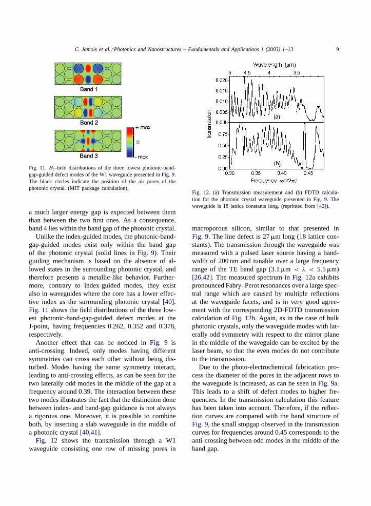
Fig. 11. Hz-field distributions of the three lowest photonic-band-gap-guided defect modes of the W1 waveguide presented inFig. 9.The black circles indicate the position of the air pores of thephotonic crystal. (MIT package calculation).
a much larger energy gap is expected between themthan between the two first ones. As a consequence,band 4 lies within the band gap of the photonic crystal.
Unlike the index-guided modes, the photonic-band-gap-guided modes exist only within the band gapof the photonic crystal (solid lines inFig. 9). Theirguiding mechanism is based on the absence of al-lowed states in the surrounding photonic crystal, andtherefore presents a metallic-like behavior. Further-more, contrary to index-guided modes, they existalso in waveguides where the core has a lower effec-tive index as the surrounding photonic crystal[40].Fig. 11shows the field distributions of the three low-est photonic-band-gap-guided defect modes at theJ-point, having frequencies 0.262, 0.352 and 0.378,respectively.
Another effect that can be noticed inFig. 9 isanti-crossing. Indeed, only modes having differentsymmetries can cross each other without being dis-turbed. Modes having the same symmetry interact,leading to anti-crossing effects, as can be seen for thetwo laterally odd modes in the middle of the gap at afrequency around 0.39. The interaction between thesetwo modes illustrates the fact that the distinction donebetween index- and band-gap guidance is not alwaysa rigorous one. Moreover, it is possible to combineboth, by inserting a slab waveguide in the middle ofa photonic crystal[40,41].
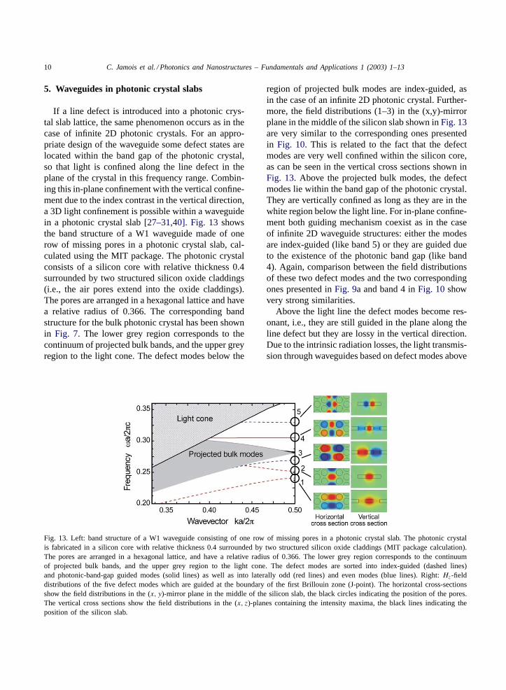
Fig. 12 shows the transmission through a W1waveguide consisting one row of missing pores in
Fig. 12. (a) Transmission measurement and (b) FDTD calcula-tion for the photonic crystal waveguide presented inFig. 9. Thewaveguide is 18 lattice constants long. (reprinted from[42]).
macroporous silicon, similar to that presented inFig. 9. The line defect is 27�m long (18 lattice con-stants). The transmission through the waveguide wasmeasured with a pulsed laser source having a band-width of 200 nm and tunable over a large frequencyrange of the TE band gap (3.1�m < λ < 5.5�m)[26,42]. The measured spectrum inFig. 12aexhibitspronounced Fabry–Perot resonances over a large spec-tral range which are caused by multiple reflectionsat the waveguide facets, and is in very good agree-ment with the corresponding 2D-FDTD transmissioncalculation ofFig. 12b. Again, as in the case of bulkphotonic crystals, only the waveguide modes with lat-erally odd symmetry with respect to the mirror planein the middle of the waveguide can be excited by thelaser beam, so that the even modes do not contributeto the transmission.
Due to the photo-electrochemical fabrication pro-cess the diameter of the pores in the adjacent rows tothe waveguide is increased, as can be seen inFig. 9a.This leads to a shift of defect modes to higher fre-quencies. In the transmission calculation this featurehas been taken into account. Therefore, if the reflec-tion curves are compared with the band structure ofFig. 9, the small stopgap observed in the transmissioncurves for frequencies around 0.45 corresponds to theanti-crossing between odd modes in the middle of theband gap.
10 C. Jamois et al. / Photonics and Nanostructures – Fundamentals and Applications 1 (2003) 1–13
5. Waveguides in photonic crystal slabs
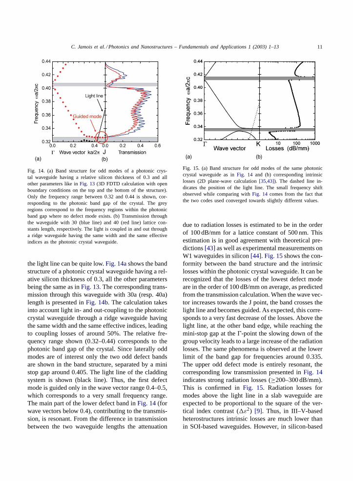
If a line defect is introduced into a photonic crys-tal slab lattice, the same phenomenon occurs as in thecase of infinite 2D photonic crystals. For an appro-priate design of the waveguide some defect states arelocated within the band gap of the photonic crystal,so that light is confined along the line defect in theplane of the crystal in this frequency range. Combin-ing this in-plane confinement with the vertical confine-ment due to the index contrast in the vertical direction,a 3D light confinement is possible within a waveguidein a photonic crystal slab[27–31,40]. Fig. 13 showsthe band structure of a W1 waveguide made of onerow of missing pores in a photonic crystal slab, cal-culated using the MIT package. The photonic crystalconsists of a silicon core with relative thickness 0.4surrounded by two structured silicon oxide claddings(i.e., the air pores extend into the oxide claddings).The pores are arranged in a hexagonal lattice and havea relative radius of 0.366. The corresponding bandstructure for the bulk photonic crystal has been shownin Fig. 7. The lower grey region corresponds to thecontinuum of projected bulk bands, and the upper greyregion to the light cone. The defect modes below the
Fig. 13. Left: band structure of a W1 waveguide consisting of one row of missing pores in a photonic crystal slab. The photonic crystalis fabricated in a silicon core with relative thickness 0.4 surrounded by two structured silicon oxide claddings (MIT package calculation).The pores are arranged in a hexagonal lattice, and have a relative radius of 0.366. The lower grey region corresponds to the continuumof projected bulk bands, and the upper grey region to the light cone. The defect modes are sorted into index-guided (dashed lines)and photonic-band-gap guided modes (solid lines) as well as into laterally odd (red lines) and even modes (blue lines). Right:Hz-fielddistributions of the five defect modes which are guided at the boundary of the first Brillouin zone (J-point). The horizontal cross-sectionsshow the field distributions in the (x, y)-mirror plane in the middle of the silicon slab, the black circles indicating the position of the pores.The vertical cross sections show the field distributions in the (x, z)-planes containing the intensity maxima, the black lines indicating theposition of the silicon slab.
region of projected bulk modes are index-guided, asin the case of an infinite 2D photonic crystal. Further-more, the field distributions (1–3) in the (x,y)-mirrorplane in the middle of the silicon slab shown inFig. 13are very similar to the corresponding ones presentedin Fig. 10. This is related to the fact that the defectmodes are very well confined within the silicon core,as can be seen in the vertical cross sections shown inFig. 13. Above the projected bulk modes, the defectmodes lie within the band gap of the photonic crystal.They are vertically confined as long as they are in thewhite region below the light line. For in-plane confine-ment both guiding mechanism coexist as in the caseof infinite 2D waveguide structures: either the modesare index-guided (like band 5) or they are guided dueto the existence of the photonic band gap (like band4). Again, comparison between the field distributionsof these two defect modes and the two correspondingones presented inFig. 9a and band 4 inFig. 10showvery strong similarities.
Above the light line the defect modes become res-onant, i.e., they are still guided in the plane along theline defect but they are lossy in the vertical direction.Due to the intrinsic radiation losses, the light transmis-sion through waveguides based on defect modes above
C. Jamois et al. / Photonics and Nanostructures – Fundamentals and Applications 1 (2003) 1–13 11
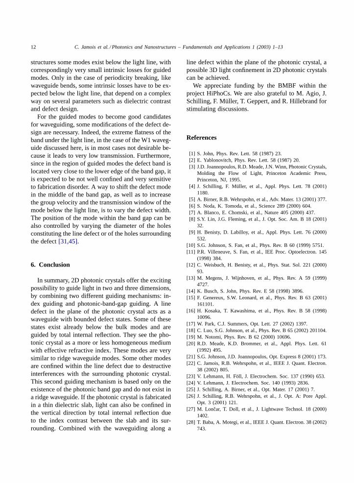
Fig. 14. (a) Band structure for odd modes of a photonic crys-tal waveguide having a relative silicon thickness of 0.3 and allother parameters like inFig. 13 (3D FDTD calculation with openboundary conditions on the top and the bottom of the structure).Only the frequency range between 0.32 and 0.44 is shown, cor-responding to the photonic band gap of the crystal. The greyregions correspond to the frequency regions within the photonicband gap where no defect mode exists. (b) Transmission throughthe waveguide with 30 (blue line) and 40 (red line) lattice con-stants length, respectively. The light is coupled in and out througha ridge waveguide having the same width and the same effectiveindices as the photonic crystal waveguide.
the light line can be quite low.Fig. 14ashows the bandstructure of a photonic crystal waveguide having a rel-ative silicon thickness of 0.3, all the other parametersbeing the same as inFig. 13. The corresponding trans-mission through this waveguide with 30a (resp. 40a)length is presented inFig. 14b. The calculation takesinto account light in- and out-coupling to the photoniccrystal waveguide through a ridge waveguide havingthe same width and the same effective indices, leadingto coupling losses of around 50%. The relative fre-quency range shown (0.32–0.44) corresponds to thephotonic band gap of the crystal. Since laterally oddmodes are of interest only the two odd defect bandsare shown in the band structure, separated by a ministop gap around 0.405. The light line of the claddingsystem is shown (black line). Thus, the first defectmode is guided only in the wave vector range 0.4–0.5,which corresponds to a very small frequency range.The main part of the lower defect band inFig. 14(forwave vectors below 0.4), contributing to the transmis-sion, is resonant. From the difference in transmissionbetween the two waveguide lengths the attenuation
Fig. 15. (a) Band structure for odd modes of the same photoniccrystal waveguide as inFig. 14 and (b) corresponding intrinsiclosses (2D plane-wave calculation[35,43]). The dashed line in-dicates the position of the light line. The small frequency shiftobserved while comparing withFig. 14 comes from the fact thatthe two codes used converged towards slightly different values.
due to radiation losses is estimated to be in the orderof 100 dB/mm for a lattice constant of 500 nm. Thisestimation is in good agreement with theoretical pre-dictions[43] as well as experimental measurements onW1 waveguides in silicon[44]. Fig. 15shows the con-formity between the band structure and the intrinsiclosses within the photonic crystal waveguide. It can berecognized that the losses of the lowest defect modeare in the order of 100 dB/mm on average, as predictedfrom the transmission calculation. When the wave vec-tor increases towards the J point, the band crosses thelight line and becomes guided. As expected, this corre-sponds to a very fast decrease of the losses. Above thelight line, at the other band edge, while reaching themini-stop gap at the�-point the slowing down of thegroup velocity leads to a large increase of the radiationlosses. The same phenomena is observed at the lowerlimit of the band gap for frequencies around 0.335.The upper odd defect mode is entirely resonant, thecorresponding low transmission presented inFig. 14indicates strong radiation losses (≥200–300 dB/mm).This is confirmed inFig. 15. Radiation losses formodes above the light line in a slab waveguide areexpected to be proportional to the square of the ver-tical index contrast (�ε2) [9]. Thus, in III–V-basedheterostructures intrinsic losses are much lower thanin SOI-based waveguides. However, in silicon-based
12 C. Jamois et al. / Photonics and Nanostructures – Fundamentals and Applications 1 (2003) 1–13
structures some modes exist below the light line, withcorrespondingly very small intrinsic losses for guidedmodes. Only in the case of periodicity breaking, likewaveguide bends, some intrinsic losses have to be ex-pected below the light line, that depend on a complexway on several parameters such as dielectric contrastand defect design.
For the guided modes to become good candidatesfor waveguiding, some modifications of the defect de-sign are necessary. Indeed, the extreme flatness of theband under the light line, in the case of the W1 waveg-uide discussed here, is in most cases not desirable be-cause it leads to very low transmission. Furthermore,since in the region of guided modes the defect band islocated very close to the lower edge of the band gap, itis expected to be not well confined and very sensitiveto fabrication disorder. A way to shift the defect modein the middle of the band gap, as well as to increasethe group velocity and the transmission window of themode below the light line, is to vary the defect width.The position of the mode within the band gap can bealso controlled by varying the diameter of the holesconstituting the line defect or of the holes surroundingthe defect[31,45].
6. Conclusion
In summary, 2D photonic crystals offer the excitingpossibility to guide light in two and three dimensions,by combining two different guiding mechanisms: in-dex guiding and photonic-band-gap guiding. A linedefect in the plane of the photonic crystal acts as awaveguide with bounded defect states. Some of thesestates exist already below the bulk modes and areguided by total internal reflection. They see the pho-tonic crystal as a more or less homogeneous mediumwith effective refractive index. These modes are verysimilar to ridge waveguide modes. Some other modesare confined within the line defect due to destructiveinterferences with the surrounding photonic crystal.This second guiding mechanism is based only on theexistence of the photonic band gap and do not exist ina ridge waveguide. If the photonic crystal is fabricatedin a thin dielectric slab, light can also be confined inthe vertical direction by total internal reflection dueto the index contrast between the slab and its sur-rounding. Combined with the waveguiding along a
line defect within the plane of the photonic crystal, apossible 3D light confinement in 2D photonic crystalscan be achieved.
We appreciate funding by the BMBF within theproject HiPhoCs. We are also grateful to M. Agio, J.Schilling, F. Müller, T. Geppert, and R. Hillebrand forstimulating discussions.
References
[1] S. John, Phys. Rev. Lett. 58 (1987) 23.[2] E. Yablonovitch, Phys. Rev. Lett. 58 (1987) 20.[3] J.D. Joannopoulos, R.D. Meade, J.N. Winn, Photonic Crystals,
Molding the Flow of Light, Princeton Academic Press,Princeton, NJ, 1995.
[4] J. Schilling, F. Müller, et al., Appl. Phys. Lett. 78 (2001)1180.
[5] A. Birner, R.B. Wehrspohn, et al., Adv. Mater. 13 (2001) 377.[6] S. Noda, K. Tomoda, et al., Science 289 (2000) 604.[7] A. Blanco, E. Chomski, et al., Nature 405 (2000) 437.[8] S.Y. Lin, J.G. Fleming, et al., J. Opt. Soc. Am. B 18 (2001)
32.[9] H. Benisty, D. Labilloy, et al., Appl. Phys. Lett. 76 (2000)
532.[10] S.G. Johnson, S. Fan, et al., Phys. Rev. B 60 (1999) 5751.[11] P.R. Villeneuve, S. Fan, et al., IEE Proc. Optoelectron. 145
(1998) 384.[12] C. Weisbuch, H. Benisty, et al., Phys. Stat. Sol. 221 (2000)
93.[13] M. Megens, J. Wijnhoven, et al., Phys. Rev. A 59 (1999)
4727.[14] K. Busch, S. John, Phys. Rev. E 58 (1998) 3896.[15] F. Genereux, S.W. Leonard, et al., Phys. Rev. B 63 (2001)
161101.[16] H. Kosaka, T. Kawashima, et al., Phys. Rev. B 58 (1998)
10096.[17] W. Park, C.J. Summers, Opt. Lett. 27 (2002) 1397.[18] C. Luo, S.G. Johnson, et al., Phys. Rev. B 65 (2002) 201104.[19] M. Notomi, Phys. Rev. B 62 (2000) 10696.[20] R.D. Meade, K.D. Brommer, et al., Appl. Phys. Lett. 61
(1992) 495.[21] S.G. Johnson, J.D. Joannopoulos, Opt. Express 8 (2001) 173.[22] C. Jamois, R.B. Wehrspohn, et al., IEEE J. Quant. Electron.
38 (2002) 805.[23] V. Lehmann, H. Föll, J. Electrochem. Soc. 137 (1990) 653.[24] V. Lehmann, J. Electrochem. Soc. 140 (1993) 2836.[25] J. Schilling, A. Birner, et al., Opt. Mater. 17 (2001) 7.[26] J. Schilling, R.B. Wehrspohn, et al., J. Opt. A: Pore Appl.
Opt. 3 (2001) 121.[27] M. Loncar, T. Doll, et al., J. Lightwave Technol. 18 (2000)
1402.[28] T. Baba, A. Motegi, et al., IEEE J. Quant. Electron. 38 (2002)
743.
C. Jamois et al. / Photonics and Nanostructures – Fundamentals and Applications 1 (2003) 1–13 13
[29] A. Talneau, L. Le Gouezigou, N. Bouadma, Opt. Lett. 26(2001) 1259.
[30] C. Weisbuch, H. Benisty, et al., IEICE Trans. Commun. 84(2001) 1286.
[31] M. Notomi, A. Shinya, et al., IEEE J. Quant. Electron. 38(2002) 736.
[32] W. Bogaerts, V. Wiaux, et al., IEEE J. Selec. Top. Quant.Electron. 8 (2002) 928.
[33] W. Bogaerts, P. Bienstman, R. Baets, Opt. Lett. 28 (2003)689.
[34] M. Qiu, Appl. Phys. Lett. 81 (2002) 1163.[35] L.C. Andreani, M. Agio, IEEE J. Quant. Electron. 38 (2002)
891.[36] M. Galli, M. Agio, et al., Eur. Phys. J. B 27 (2002) 79.
[37] T. Ochiai, K. Sakoda, Phys. Rev. B 63 (2001) 125107.[38] M. Qiu, B. Jaskorzynska, et al., Micr. Opt. Technol. Lett. 34
(2002) 387.[39] C.T. Chan, Q.L. Yu, K.M. Ho, Phys. Rev. B 51 (1995) 16635.[40] S.G. Johnson, P. Villeneuve, et al., Phys. Rev. B 62 (2000)
8212.[41] W.T. Lau, S. Fan, Appl. Phys. Lett. 81 (2002) 3915.[42] S.W. Leonard, H.M. van Driel, et al., Opt. Lett. 25 (2000)
1550.[43] L.C. Andreani, M. Agio, Appl. Phys. Lett. 82 (2003) 2011[44] M. Loncar, D. Nedeljkovic, et al., Appl. Phys. Lett. 80 (2002)
1689.[45] M. Loncar, J. Vuckovic, A. Scherer, J. Opt. Soc. Am. B 18
(2001) 1362.