review - jeiltrans.comjeiltrans.com/data/file/br_21/1917192400_jvsfgzgd_56.pdf · cells,14–17...
TRANSCRIPT

Copyright © 2014 American Scientific PublishersAll rights reservedPrinted in the United States of America
ReviewJournal of
Nanoscience and NanotechnologyVol. 14, 1282–1302, 2014
www.aspbs.com/jnn
Fabrication of One-Dimensional Organic Nanomaterials
and Their Optoelectronic Applications
Hojeong Yu1, Dong Yeong Kim1, Kyung Jin Lee2�∗, and Joon Hak Oh1�∗1School of Nano-Bioscience and Chemical Engineering, KIER-UNIST Advanced Center for Energy, Low Dimensional
Carbon Materials Center, Ulsan National Institute of Science and Technology (UNIST), Ulsan, 689-798, Korea2Department of Fine Chemical Engineering and Applied Chemistry, College of Engineering,
Chungnam National University, Yuseong-gu, Daejeon, 305-764, Korea
This paper reviews the recent research and development of one-dimensional (1D) organic nano-materials synthesized from organic semiconductors or conducting polymers and their applicationsto optoelectronics. We introduce synthetic methodologies for the fabrication of 1D single-crystallineorganic nanomaterials and 1D multi-component organic nanostructures, and discuss their opticaland electrical properties. In addition, their versatile applications in optoelectronics are highlighted.The fabrication of highly crystalline organic nanomaterials combined with their integration into nano-electronic devices is recognized as one of the most promising strategies to enhance charge trans-port properties and achieve device miniaturization. In the last part of this review, we discuss thechallenges and the perspectives of organic nanomaterials for applications in the next generationsoft electronics, in terms of fabrication, processing, device integration, and investigation on thefundamental mechanisms governing the charge transport behaviors of these advanced materials.
Keywords: Organic Nanomaterials, Organic Electronics, Organic Semiconductors, One-Dimensional Nanomaterials, Single Crystals, Organic Nanowires, Optoelectronics.
CONTENTS1. Introduction . . . . . . . . . . . . . . . . . . . . . . . . . . . . . . . . . . . . . . . . 1282
2. Fabrication of 1D Organic Nanomaterials . . . . . . . . . . . . . . . . . 1284
2.1. Self-Assembly in Solution Phase . . . . . . . . . . . . . . . . . . . . 1284
2.2. Self-Assembly in Vapor Phase . . . . . . . . . . . . . . . . . . . . . . 1286
2.3. Template-Assisted Synthesis . . . . . . . . . . . . . . . . . . . . . . . 1288
2.4. Electrospinning . . . . . . . . . . . . . . . . . . . . . . . . . . . . . . . . . 1289
3. Optoelectronic Applications of Organic Nanomaterials . . . . . . . 1293
3.1. Optoelectronic Devices Based on Single-Component
Organic Nanomaterials . . . . . . . . . . . . . . . . . . . . . . . . . . . . 1293
3.2. Energy Harvesting Devices Based on Single-Component
Organic Nanomaterials . . . . . . . . . . . . . . . . . . . . . . . . . . . . 1296
3.3. Optoelectronics Based on
Multi-Component Nanomaterials . . . . . . . . . . . . . . . . . . . . 1297
4. Concluding Remarks . . . . . . . . . . . . . . . . . . . . . . . . . . . . . . . . . 1299
References and Notes . . . . . . . . . . . . . . . . . . . . . . . . . . . . . . . . 1300
1. INTRODUCTIONOrganic semiconducting materials have attracted great
interest because of their various advantages such as
large-scale synthesis, solution processability, and simple
∗Authors to whom correspondence should be addressed.
electronic tunability by molecular design. Furthermore,
their compatibility with flexible and lightweight substrates
enables their versatile implementation to the electronic cir-
cuits, energy and bio-related applications.1–3 In particular,
organic semiconductors based on �-conjugated molecules
can be easily transformed into one-dimensional (1D)
nanostructures that can potentially exhibit novel optical,
electrical, and chemical properties.4–6 Examples of these
assemblies include nanowires (NWs), nanorods, nanorib-
bons, nanobelts, whiskers, and nanotubes. In general, 1D
organic nanostructures can be fabricated with various
methods including solution-phase synthesis, vapor-phase
synthesis, template-assisted synthesis, electrospinning,
nanolithography, soft lithography, and so on. In particular,
1D nanostructures based on organic semiconductors have
a large surface-to-volume ratio compared to bulk mate-
rials and possess a highly crystalline nature that is ben-
eficial to efficient charge transport. To date, 1D organic
nanomaterials based on organic semiconductors and con-
ducting polymers have shown great potential in diverse
applications covering organic light-emitting diodes,7 field-
effect transistors,4�8–11 phototransistors,12�13 photovoltaic
1282 J. Nanosci. Nanotechnol. 2014, Vol. 14, No. 2 1533-4880/2014/14/1282/021 doi:10.1166/jnn.2014.9086
Yu et al. Fabrication of One-Dimensional Organic Nanomaterials and Their Optoelectronic Applications
cells,14–17 nanoscale lasers,18�19 memory devices,20 and
sensors.21 To integrate 1D organic nanostructures into
device applications, they need to be well-aligned and
assembled in desired positions.22–24
In addition to the synthesis of conventional single-
component 1D nanostructures, the concepts of multi-
component nanomaterials such as p–n junctions, core–shell
NWs, composites and multi-shape nanostructures such as
porous, branched structures, hollow structures have been
recently suggested. Progress in nanoscale heterostructures
is important for optoelectronic applications as well as for
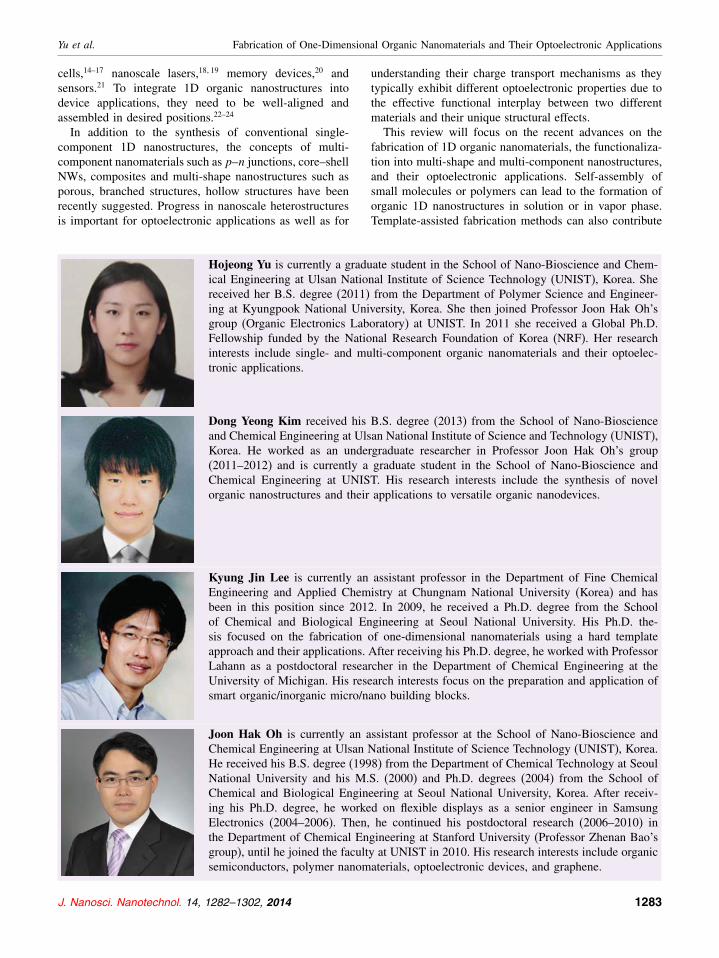
Hojeong Yu is currently a graduate student in the School of Nano-Bioscience and Chem-
ical Engineering at Ulsan National Institute of Science Technology (UNIST), Korea. She
received her B.S. degree (2011) from the Department of Polymer Science and Engineer-
ing at Kyungpook National University, Korea. She then joined Professor Joon Hak Oh’s
group (Organic Electronics Laboratory) at UNIST. In 2011 she received a Global Ph.D.
Fellowship funded by the National Research Foundation of Korea (NRF). Her research
interests include single- and multi-component organic nanomaterials and their optoelec-
tronic applications.
Dong Yeong Kim received his B.S. degree (2013) from the School of Nano-Bioscience
and Chemical Engineering at Ulsan National Institute of Science and Technology (UNIST),
Korea. He worked as an undergraduate researcher in Professor Joon Hak Oh’s group
(2011–2012) and is currently a graduate student in the School of Nano-Bioscience and
Chemical Engineering at UNIST. His research interests include the synthesis of novel
organic nanostructures and their applications to versatile organic nanodevices.
Kyung Jin Lee is currently an assistant professor in the Department of Fine Chemical
Engineering and Applied Chemistry at Chungnam National University (Korea) and has
been in this position since 2012. In 2009, he received a Ph.D. degree from the School
of Chemical and Biological Engineering at Seoul National University. His Ph.D. the-
sis focused on the fabrication of one-dimensional nanomaterials using a hard template
approach and their applications. After receiving his Ph.D. degree, he worked with Professor
Lahann as a postdoctoral researcher in the Department of Chemical Engineering at the
University of Michigan. His research interests focus on the preparation and application of
smart organic/inorganic micro/nano building blocks.
Joon Hak Oh is currently an assistant professor at the School of Nano-Bioscience and
Chemical Engineering at Ulsan National Institute of Science Technology (UNIST), Korea.
He received his B.S. degree (1998) from the Department of Chemical Technology at Seoul
National University and his M.S. (2000) and Ph.D. degrees (2004) from the School of
Chemical and Biological Engineering at Seoul National University, Korea. After receiv-
ing his Ph.D. degree, he worked on flexible displays as a senior engineer in Samsung
Electronics (2004–2006). Then, he continued his postdoctoral research (2006–2010) in
the Department of Chemical Engineering at Stanford University (Professor Zhenan Bao’s
group), until he joined the faculty at UNIST in 2010. His research interests include organic
semiconductors, polymer nanomaterials, optoelectronic devices, and graphene.
understanding their charge transport mechanisms as they
typically exhibit different optoelectronic properties due to
the effective functional interplay between two different
materials and their unique structural effects.
This review will focus on the recent advances on the
fabrication of 1D organic nanomaterials, the functionaliza-
tion into multi-shape and multi-component nanostructures,
and their optoelectronic applications. Self-assembly of
small molecules or polymers can lead to the formation of
organic 1D nanostructures in solution or in vapor phase.
Template-assisted fabrication methods can also contribute
J. Nanosci. Nanotechnol. 14, 1282–1302, 2014 1283
Fabrication of One-Dimensional Organic Nanomaterials and Their Optoelectronic Applications Yu et al.
to the growth of 1D nanostructures in both phases.
In the following section, an electrospinning method with
the applications of electrospun fibers will be discussed.
Furthermore, this review will address advantages of opto-
electronic devices based on single-component or multi-
component nanomaterials in comparison with bulk and
thin-film based electronics. Finally, concluding remarks
about 1D organic nanomaterials and their future perspec-
tives in optoelectronic applications will be discussed.
2. FABRICATION OF 1DORGANIC NANOMATERIALS
2.1. Self-Assembly in Solution PhaseSelf-assembly of �-conjugated molecules into 1D nano-
structures is generally dependent upon the balance of
the �–� interaction of �-conjugated backbone and the
hydrophobic interaction between alkyl side chains. Typ-
ically, 1D organic nanostructures can be successfully
obtained via strong co-facial �–� stacking interactions,
while reducing the unfavorable lateral growth driven
by hydrophobic interactions between alkyl side chains.25
Strong intermolecular coupling between the �-stacked
molecules provides an efficient pathway for charge trans-
port along the long axis of NW. 1D organic nanostructures
can be synthesized in various forms such as wires, rods,
ribbons, tubes, and belts via solution-phase self-assembly.
Conjugated organic semiconducting materials with
low solubility in organic solvent can self-assemble
into 1D structures via recrystallization. A representative
n-type organic semiconductor, N ,N ′-bis(2-phenylethyl)-perylene-3,4:9,10-tetracarboxylic diimide (BPE-PTCDI) is
sparingly soluble in a common organic solvent such as
o-dichlorobenzene and benzonitrile at room temperature,
whereas it becomes soluble upon heating with reflux-
ing. BPE-PTCDI molecules tend to self-assemble into
needle-like 1D structures via strong �–� interactions of
�-conjugated backbones upon cooling the hot, homoge-
neous solution. Furthermore, the diameter and the length
of BPE-PTCDI wires can be tuned across a wide range
by controlling the cooling speed and the nucleation den-
sity tunable by the non-solvent (i.e., methyl alcohol) mix-
ing ratio. The size of BPE-PTCDI wires can be easily
tuned, ranging from several tens of nanometers to several
micrometers in diameter and several tens of micrometers
to several millimeters in length (Fig. 1(a)). The structural
characterization with transmission electron microscopy
(TEM) revealed that BPE-PTCDI molecules self-assemble
into 1D nanostructures with the �-planar distance of 3.4 Å
(Figs. 1(b) and (c)).11
The above-mentioned, non-solvent-mediated recrystal-
lization method is also applicable to the preparation of
highly conjugated p-channel organic semiconductors such
as hexathiapentacene (HTP).8 Furthermore, 1-cyano-trans-1,2-bis-(3′�5′-bis-trifluoromethyl-biphenyl)ethylene (CN-
TFMBE) molecules can self-assemble in a mixture solvent
of o-dichlorobenzene and methyl alcohol via recrystalliza-
tion spin coating or drop-casting into highly fluorescent 1D
nanomaterials, which is driven by the interactions between
cyano-stilbene backbone and terminal –CF3 units.26�27 The
CN-TFMBE NWs were synthesized with diameters around
100 nm and showed enhanced fluorescence emission in
the solid state, as shown in Figures 1(d) and (e). The
strong intermolecular �–� stacking was induced by the
planarization of the CN-TFMBE owing to the CN group
and CF3 end groups (Fig. 1(f)).
In the case of organic semiconducting molecules, which
are highly soluble in organic solvents, 1D nanostruc-
tured self-assemblies can be prepared by transferring
the molecules from a good solvent to a non-solvent,
followed by rapid dispersion.28 This method refers to
rapid solution dispersion method. The propoxylethyl-
perylene-3,4,9,10-tetracarboxylic-3,4,9,10-diimide (propo-
xylethyl-PTCDI) molecules have sufficient solubility in
hydrophobic solvents such as chloroform, due to the
flexible propoxyethyl side chain. The concentrated solu-
tion can readily self-assemble to form nanobelt crys-
tals upon injection of a small amount of solution into
methanol.29 Similarly, injection of a small volume of
concentrated 6,13-bis(triisopropylsilylethynyl) pentacene
(TIPS-PEN)/toluene solution into acetonitrile can lead to
the formation of TIPS-PEN microribbon through the self-
assembly on the basis of rapid solution dispersion method
(Figs. 1(g)–(i)).9
When conjugated molecules have different solubility in
two organic solvents, self-assembly can be induced at the
interface between two different solvents through binary
phase transfer. The solvent interface is typically formed
by the difference in the polarity and the density of two
solvents. PTCDI molecules with alkyl side chains (PTCDI-
Cn� can be transformed into 1D nanostructures via the
self-assembly at the methyl alcohol/chloroform interface.8
Moreover, solvent vapor diffusion can be used to
form 1D organic single crystals. Lv et al. reported the
organic single crystal of the tetrachlorinated diperylene
bisimide (C12-4CldiPBI) grown by solvent vapor diffusion
method.30 The C12-4CldiPBI solution dissolved in toluene
was prepared in a small vial and exposed to methyl alcohol
vapor. The nanoribbons with a diameter of around 2 �mwere obtained after 3 days.
Moreover, Goto et al. reported a novel method to fab-
ricate organic single-crystal arrays with a large-scale from
solution-phase synthesis.31 They prepared aligned organic
single-crystal arrays by controlling the supersaturation
region of 3,9-bis(4-ethylphenyl)-peri-xanthenoxanthene
(C2Ph-PXX) solution. In the specific micropatterns, the
supersaturation of organic solution could be changed
locally, leading to the formation of single crystals (Fig. 2).
This simple method allowed the formation of the aligned
organic single crystal arrays. The careful control of the
micropatterns may provide the formation of 1D single
crystals.
1284 J. Nanosci. Nanotechnol. 14, 1282–1302, 2014
Yu et al. Fabrication of One-Dimensional Organic Nanomaterials and Their Optoelectronic Applications
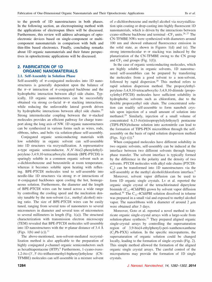
Figure 1. (a) Bright field and dark field (inset) OM images of BPE-PTCDI NWs, (b) TEM image and SAED pattern (inset), and (c) schematic
diagram of molecular packing analysis of single BPE-PTCDI NW. (a)–(c) Reprinted with permission from [12], H. Yu, et al., Adv. Funct. Mater. 23, 629(2013). © 2013, Wiley-VCH. (d) Scanning electron microscopy image of CN-TFMBE NWs, (e) fluorescence microscopy image and fluorescence image
(inset) of molecular state (denoted as I) and nanostructured CN-TFMBE (denoted as A), (f) schematic diagram of molecular packing of CN-TFMBE
NW. (d)–(f) Reprinted with permission from [26], B. K. An, et al., J. Am. Chem. Soc. 131, 3950 (2009). © 2009, American Chemical Society. (g) SEM
image of a micro-ribbon of TIPS-PEN, (h) its selected area diffraction (SAED) pattern, and (i) the molecular packing analysis. (g)–(i) Reprinted with
permission from [9], D. H. Kim, et al., Adv. Mater. 19, 678 (2007). © 2007, Wiley-VCH.
A wide range of approaches have also been utilized
to prepare 1D self-assembled crystalline polymer nano-
structures. Poly-(3-alkylthiophene) (P3AT) NWs could be
obtained by the thermally induced crystallization of P3AT
in a poor solvent.32 The crystallization of �-conjugated
polymers, which contain electron-rich backbones and
aliphatic chains, is usually prohibited by the entangled
chain conformations.5 Most of the related reports have
focused on only the fabrication of nanostructured P3ATs
because of their strong self-organizing characteristics.
Highly crystalline 1D polymer NWs with low solubil-
ity in organic solvent can be synthesized in a dilute solu-
tion (0.05∼1%). By heating the mixture of highly diluted
P3AT solution with poor solvent, followed by a cooling
process, conjugated molecules can be stacked via �–�interaction between aromatic backbones without unfavor-
able stacking from aliphatic chains. P3AT NWs can be
obtained in various conditions; controlling the length of
alkyl chain, molecular weight, concentration, crystalliza-
tion temperature, solvent, and regioregularity of polymer
materials in an initial good solvent to a marginal or poor
solvent.6
Kiriy et al. reported the formation of NWs by the aggre-
gation of regioregular head-to-tail P3ATs by using a selec-
tive solvent, hexane, which is a good solvent for alkyl
chains, but a poor solvent for polythiophene backbones.33
The addition of hexane into the chloroform solution of
P3AT induced an ordered aggregation of the P3AT main-
chain driven by a solvophobic interaction. Kim et al.
reported a self-seeding method of poly(3-hexylthiophene)
(P3HT) with a dilute solution in chloroform to fabricate
1D microwires (MWs).34 Slow cooling the solution from
40 �C to 10 �C over three days created crystalline seeds
in solution to facilitate the growth of P3HT MWs in a
solution phase. Figure 3(a) shows the polarized OM image
and SEM images of 1D single-crystalline P3HT MWs. The
width and length of the wires were approximately 1–3 �mand 30–500 �m, respectively. The molecular and crystallo-
graphic structures of P3HT chains in a single-crystal MW
are depicted in Figure 3(b).
Aside from P3AT single crystalline NWs, several
different semiconducting polymers can be utilized to
fabricate 1D nanostructures in solution phase. Dong
et al. fabricated highly crystalline NWs using poly
J. Nanosci. Nanotechnol. 14, 1282–1302, 2014 1285
Fabrication of One-Dimensional Organic Nanomaterials and Their Optoelectronic Applications Yu et al.
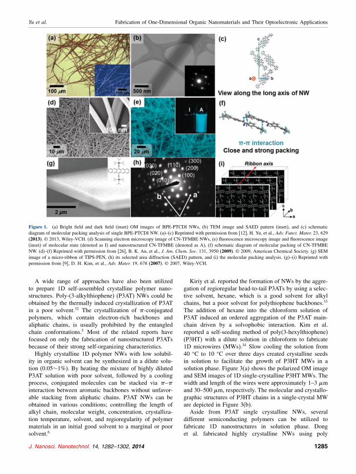
Figure 2. (a) Schematic diagram of the solubility-supersolubility relationship. Points ABC represent three states of solution at the same temperature
with different solution concentrations; point A is a stable state, where crystallization does not occur. As the concentration increases over solubility
curve, crystallization occurs at points B and C. The spontaneous crystallization can occur at point C because nucleation occurs only in a supersaturated
solution. (b) Schematic diagram of crystal growth in the nucleation control region. (c) Two regions of the micropattern; nucleation control region and
growth control region (up) and the schematic growth model (bottom). (d) Polarized OM image of well-aligned 12× 32 arrays of C2Ph-PXX films.
Reprinted with permission from [31], O. Goto, et al., Adv. Mater. 24, 1117 (2012). © 2012, Wiley-VCH.
(para-phenylene ethynylene) derivatives with thioacetate
end groups (TA-PPE) via slow self-assembly from a
dilute solution (0.05–1.0 mg ml−1� under a volatile sol-
vent pressure in a closed jar.35 Slow evaporation of
the solvent could induce self-assembly of the polymer
molecules with strong intermolecular interactions. Large-
area and well-defined TA-PPE NWs were obtained through
the self-assembly of TA-PPE in tetrahydrofuran (THF)
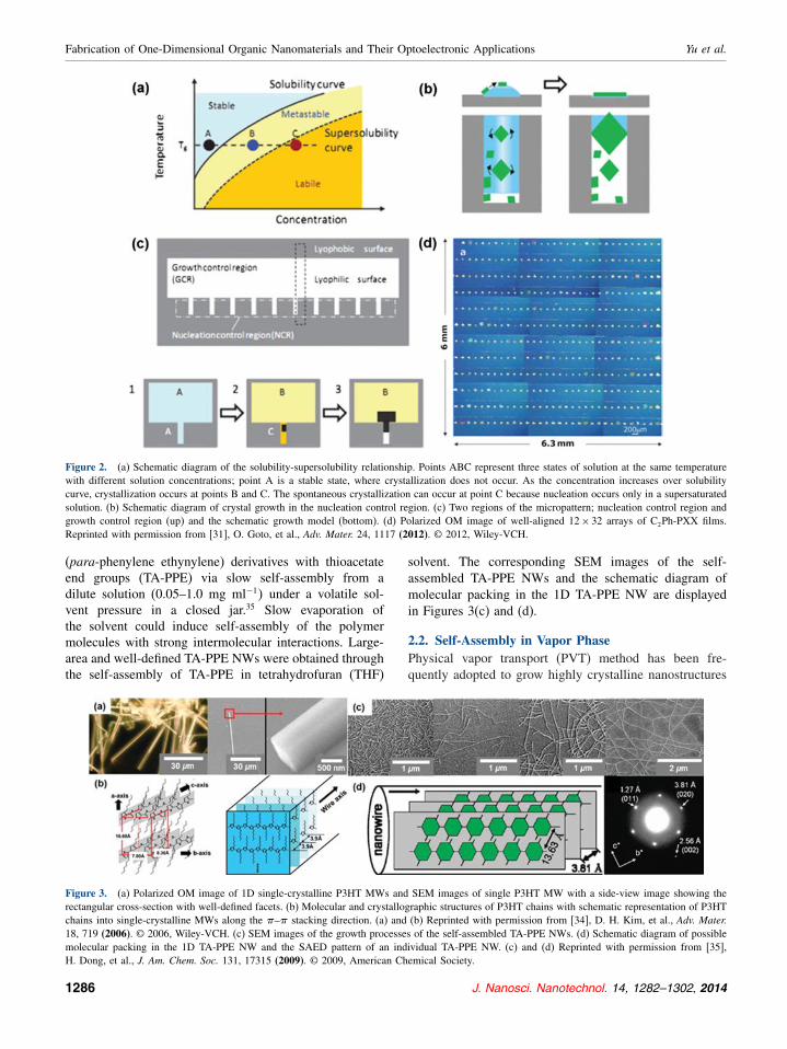
Figure 3. (a) Polarized OM image of 1D single-crystalline P3HT MWs and SEM images of single P3HT MW with a side-view image showing the
rectangular cross-section with well-defined facets. (b) Molecular and crystallographic structures of P3HT chains with schematic representation of P3HT
chains into single-crystalline MWs along the �–� stacking direction. (a) and (b) Reprinted with permission from [34], D. H. Kim, et al., Adv. Mater.18, 719 (2006). © 2006, Wiley-VCH. (c) SEM images of the growth processes of the self-assembled TA-PPE NWs. (d) Schematic diagram of possible
molecular packing in the 1D TA-PPE NW and the SAED pattern of an individual TA-PPE NW. (c) and (d) Reprinted with permission from [35],
H. Dong, et al., J. Am. Chem. Soc. 131, 17315 (2009). © 2009, American Chemical Society.
solvent. The corresponding SEM images of the self-
assembled TA-PPE NWs and the schematic diagram of
molecular packing in the 1D TA-PPE NW are displayed
in Figures 3(c) and (d).
2.2. Self-Assembly in Vapor PhasePhysical vapor transport (PVT) method has been fre-
quently adopted to grow highly crystalline nanostructures
1286 J. Nanosci. Nanotechnol. 14, 1282–1302, 2014
Yu et al. Fabrication of One-Dimensional Organic Nanomaterials and Their Optoelectronic Applications
of organic semiconductors that are insoluble in common
organic solvents. The main advantage of this method is
that the direct growth on any substrates can be realized
with less contamination. In a typical PVT process, quartz
tubes are loaded in a furnace with a temperature gradi-
ent. Then, organic semiconductors are sublimated at the
high-temperature region and the vaporized molecules are
carried by the flow of inert gas to the lower temperature
region. Then, the nucleation of the crystal growth takes
place at the lower temperature region, eventually leading
to the formation of highly purified crystals.
High-purity single crystals can be obtained from the
PVT method without unintentional doping, which is gen-
erally caused by solvent molecules or other impurities.
Moreover, this method can be employed to induce the
direct growth of highly crystalline organic semiconduc-
tor nanomaterials onto a desired substrate. Similarly, the
deposition of thin films or crystals by the condensation of
vaporized target materials onto surfaces is defined as the
physical vapor deposition (PVD) method. Because single
crystals fabricated in a vapor phase are free of defect or
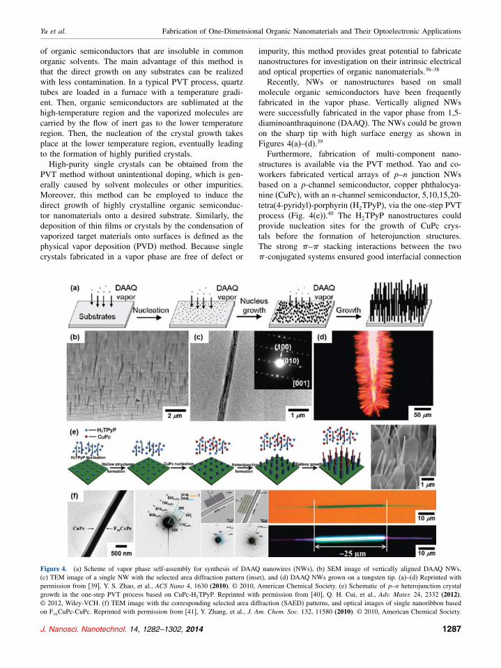
Figure 4. (a) Scheme of vapor phase self-assembly for synthesis of DAAQ nanowires (NWs), (b) SEM image of vertically aligned DAAQ NWs,
(c) TEM image of a single NW with the selected area diffraction pattern (inset), and (d) DAAQ NWs grown on a tungsten tip. (a)–(d) Reprinted with
permission from [39], Y. S. Zhao, et al., ACS Nano 4, 1630 (2010). © 2010, American Chemical Society. (e) Schematic of p–n heterojunction crystal
growth in the one-step PVT process based on CuPc-H2TPyP. Reprinted with permission from [40], Q. H. Cui, et al., Adv. Mater. 24, 2332 (2012).© 2012, Wiley-VCH. (f) TEM image with the corresponding selected area diffraction (SAED) patterns, and optical images of single nanoribbon based
on F16CuPc-CuPc. Reprinted with permission from [41], Y. Zhang, et al., J. Am. Chem. Soc. 132, 11580 (2010). © 2010, American Chemical Society.
impurity, this method provides great potential to fabricate
nanostructures for investigation on their intrinsic electrical
and optical properties of organic nanomaterials.36–38
Recently, NWs or nanostructures based on small
molecule organic semiconductors have been frequently
fabricated in the vapor phase. Vertically aligned NWs
were successfully fabricated in the vapor phase from 1,5-
diaminoanthraquinone (DAAQ). The NWs could be grown
on the sharp tip with high surface energy as shown in
Figures 4(a)–(d).39
Furthermore, fabrication of multi-component nano-
structures is available via the PVT method. Yao and co-
workers fabricated vertical arrays of p–n junction NWs
based on a p-channel semiconductor, copper phthalocya-
nine (CuPc), with an n-channel semiconductor, 5,10,15,20-
tetra(4-pyridyl)-porphyrin (H2TPyP), via the one-step PVT
process (Fig. 4(e)).40 The H2TPyP nanostructures could
provide nucleation sites for the growth of CuPc crys-
tals before the formation of heterojunction structures.
The strong �–� stacking interactions between the two
�-conjugated systems ensured good interfacial connection
J. Nanosci. Nanotechnol. 14, 1282–1302, 2014 1287
Fabrication of One-Dimensional Organic Nanomaterials and Their Optoelectronic Applications Yu et al.
at the junction part. Briseno and co-workers reported the
fabrication of F16CuPc-CuPc nanoribbons (Fig. 4(f)) and
found that the selective growth behaviors of vaporized
molecules into crystals are strongly dependent upon the
similarity in molecular structures and lattice parameters at
the interfacial basal planes.41
Furthermore, dendritic organic heterojunctions with alu-
minum tris(8-hydroxyquinoline) (Alq3� MW trunks and
DAAQ NW branches were prepared with the two-step
PVD growth process.42 In this system, the Alq3 MWs were
used as seeds for the vertical growth of DAAQ NWs. Simi-
larly, Yan et al. reported the site-selective growth behaviors
of 4,4′-bis(phenylethynyl)anthracene (BPEA) NWs using
the PVD method.43 The condensation of vaporized BPEA
molecules took place on the sharp tips of silver NWs.
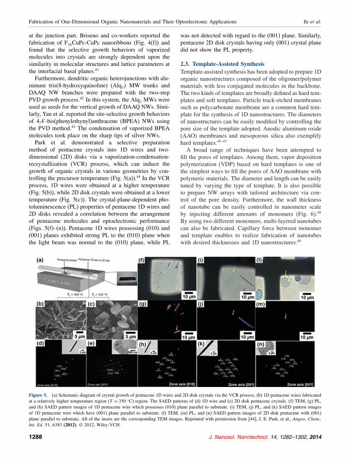
Park et al. demonstrated a selective preparation
method of pentacene crystals into 1D wires and two-
dimensional (2D) disks via a vaporization-condensation-
recrystallization (VCR) process, which can induce the
growth of organic crystals in various geometries by con-
trolling the precursor temperature (Fig. 5(a)).44 In the VCR
process, 1D wires were obtained at a higher temperature
(Fig. 5(b)), while 2D disk crystals were obtained at a lower
temperature (Fig. 5(c)). The crystal-plane-dependent pho-
toluminescence (PL) properties of pentacene 1D wires and
2D disks revealed a correlation between the arrangement
of pentacene molecules and optoelectronic performance
(Figs. 5(f)–(n)). Pentacene 1D wires possessing (010) and
(001) planes exhibited strong PL to the (010) plane when
the light beam was normal to the (010) plane, while PL
Figure 5. (a) Schematic diagram of crystal growth of pentacene 1D wires and 2D disk crystals via the VCR process, (b) 1D pentacene wires fabricated
at a relatively higher temperature region (T = 350 �C) region. The SAED patterns of (d) 1D wire and (e) 2D disk pentacene crystals. (f) TEM, (g) PL,
and (h) SAED pattern images of 1D pentacene wire which possesses (010) plane parallel to substrate. (i) TEM, (j) PL, and (k) SAED pattern images
of 1D pentacene wire which have (001) plane parallel to substrate. (l) TEM, (m) PL, and (n) SAED pattern images of 2D disk pentacene with (001)
plane parallel to substrate. All of the insets are the corresponding TEM images. Reprinted with permission from [44], J. E. Park, et al., Angew. Chem.,Int. Ed. 51, 6383 (2012). © 2012, Wiley-VCH.
was not detected with regard to the (001) plane. Similarly,
pentacene 2D disk crystals having only (001) crystal plane
did not show the PL property.
2.3. Template-Assisted SynthesisTemplate-assisted synthesis has been adopted to prepare 1D
organic nanostructures composed of the oligomer/polymer
materials with less conjugated molecules in the backbone.
The two kinds of templates are broadly defined as hard tem-
plates and soft templates. Particle track-etched membranes
such as polycarbonate membrane are a common hard tem-
plate for the synthesis of 1D nanostructures. The diameters
of nanostructures can be easily modified by controlling the
pore size of the template adopted. Anodic aluminum oxide
(AAO) membranes and mesoporous silica also exemplify
hard templates.45–47
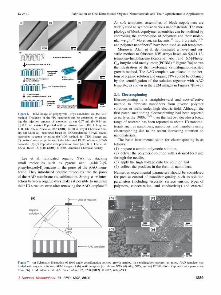
A broad range of techniques have been attempted to
fill the pores of templates. Among them, vapor deposition
polymerization (VDP) based on hard templates is one of
the simplest ways to fill the pores of AAO membrane with
polymeric materials. The diameter and length can be easily
tuned by varying the type of template. It is also possible
to prepare NW arrays with tailored architecture via con-
trol of the pore density. Furthermore, the wall thickness
of nanotube can be easily controlled in nanometer scale
by injecting different amounts of monomers (Fig. 6).48
By using two different monomers, multi-layered nanotubes
can also be fabricated. Capillary force between monomer
and template enables to realize fabrication of nanotubes
with desired thicknesses and 1D nanostructures.49
1288 J. Nanosci. Nanotechnol. 14, 1282–1302, 2014
Yu et al. Fabrication of One-Dimensional Organic Nanomaterials and Their Optoelectronic Applications
Figure 6. TEM image of polypyrrole (PPy) nanotubes via the VDP
method. Thickness of the PPy nanotubes can be controlled by chang-
ing the injection amount of monomer as (a) 0.07 ml, (b) 0.14 ml,
(c) 0.21 ml. (a)–(c) Reprinted with permission from [48], J. Jang and
J. H. Oh, Chem. Commun. 882 (2004). © 2004, Royal Chemical Soci-
ety. (d) Multi-cell nanotubes based on PAN/rhodamine B/PAN coaxial
nanotubes structure by using the VDP method. (e) TEM images and
(f) confocal microscope image of the fabricated PAN/rhodamine B/PAN
nanotube. (d)–(f) Reprinted with permission from [49], K. J. Lee, et al.,
Chem. Mater. 18, 5002 (2006). © 2006, American Chemical Society.
Lee et al. fabricated organic NWs by stacking
small molecules such as pyrene and 1,4-bis[2-(5-
phenyloxazolyl)]benzene in the pores of the AAO mem-
brane. They introduced organic molecules into the pores
of the AAO membrane via sublimation. Strong �–� inter-
action between organic dyes makes it possible to maintain
their 1D structure even after removing the AAO template.50
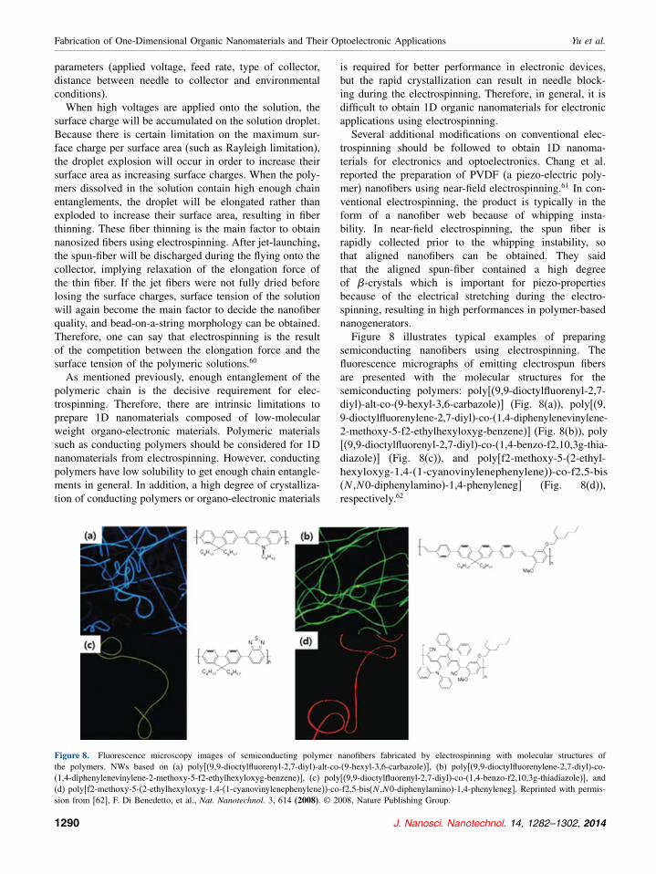
Figure 7. (a) Schematic illustration of fixed-angle centrifugation-assisted growth method. In centrifugation process, an empty AAO template was
loaded with organic solutions. SEM images of (b) AAO template (c) rubrene NWs (d) Alq3 NWs, and (e) PCBM NWs. Reprinted with permission
from [56], K. M. Alam, et al., Adv. Funct. Mater. 22, 3298 (2012). © 2012, Wiley-VCH.
As soft templates, assemblies of block copolymers are
widely used to synthesize various nanomaterials. The mor-
phology of block copolymer assemblies can be modified by
controlling the composition of polymers and their molec-
ular weight.51 Moreover, surfactants,52 liquid crystals,53�54
and polymer nanofibers55 have been used as soft templates.
Moreover, Alam et al. demonstrated a novel and ver-
satile method to fabricate NW arrays based on 5,6,11,12-
tetraphenylnaphthacene (Rubrene), Alq3, and [6,6]-Phenyl
C61 butyric acid methyl ester (PCBM).56 Figure 7(a) shows
the illustration of the fixed-angle centrifugation-assisted
growth method. The AAO template was placed in the bot-
tom of organic solution and organic NWs could be obtained
by the centrifugation of the solution together with AAO
template, as shown in the SEM images in Figures 7(b)–(e).
2.4. ElectrospinningElectrospinning is a straightforward and cost-effective
method to fabricate nanofibers from diverse polymer
solutions or melts under high electric field. Although the
first patent mentioning electrospinning had been reported
as early as the 1900s,57–59 over the last two decades a broad
range of research has been reported to obtain 1D nanoma-
terials such as nanofibers, nanotubes, and nanobelts using
electrospinning due to the recent increasing attention on
nanomaterials.
The basic instrumental setup for electrospinning is as
follows:
(1) prepare a certain polymeric solution,
(2) deliver the polymeric solution with a desired feed rate
through the needle,
(3) apply the high voltage onto the solution and
(4) collect the products in the form of nanofibers.
Numerous experimental parameters should be considered
for precise control of nanofiber quality, such as solution
parameters (including viscosity, surface tension, types of
polymers, concentration, and conductivity) and external
J. Nanosci. Nanotechnol. 14, 1282–1302, 2014 1289
Fabrication of One-Dimensional Organic Nanomaterials and Their Optoelectronic Applications Yu et al.
parameters (applied voltage, feed rate, type of collector,
distance between needle to collector and environmental
conditions).
When high voltages are applied onto the solution, the
surface charge will be accumulated on the solution droplet.
Because there is certain limitation on the maximum sur-
face charge per surface area (such as Rayleigh limitation),
the droplet explosion will occur in order to increase their
surface area as increasing surface charges. When the poly-
mers dissolved in the solution contain high enough chain
entanglements, the droplet will be elongated rather than
exploded to increase their surface area, resulting in fiber
thinning. These fiber thinning is the main factor to obtain
nanosized fibers using electrospinning. After jet-launching,
the spun-fiber will be discharged during the flying onto the
collector, implying relaxation of the elongation force of
the thin fiber. If the jet fibers were not fully dried before
losing the surface charges, surface tension of the solution
will again become the main factor to decide the nanofiber
quality, and bead-on-a-string morphology can be obtained.
Therefore, one can say that electrospinning is the result
of the competition between the elongation force and the
surface tension of the polymeric solutions.60
As mentioned previously, enough entanglement of the
polymeric chain is the decisive requirement for elec-
trospinning. Therefore, there are intrinsic limitations to
prepare 1D nanomaterials composed of low-molecular
weight organo-electronic materials. Polymeric materials
such as conducting polymers should be considered for 1D
nanomaterials from electrospinning. However, conducting
polymers have low solubility to get enough chain entangle-
ments in general. In addition, a high degree of crystalliza-
tion of conducting polymers or organo-electronic materials
Figure 8. Fluorescence microscopy images of semiconducting polymer nanofibers fabricated by electrospinning with molecular structures of
the polymers. NWs based on (a) poly[(9,9-dioctylfluorenyl-2,7-diyl)-alt-co-(9-hexyl-3,6-carbazole)], (b) poly[(9,9-dioctylfluorenylene-2,7-diyl)-co-
(1,4-diphenylenevinylene-2-methoxy-5-f2-ethylhexyloxyg-benzene)], (c) poly[(9,9-dioctylfluorenyl-2,7-diyl)-co-(1,4-benzo-f2,10,3g-thiadiazole)], and
(d) poly[f2-methoxy-5-(2-ethylhexyloxyg-1,4-(1-cyanovinylenephenylene))-co-f2,5-bis(N ,N0-diphenylamino)-1,4-phenyleneg]. Reprinted with permis-
sion from [62], F. Di Benedetto, et al., Nat. Nanotechnol. 3, 614 (2008). © 2008, Nature Publishing Group.
is required for better performance in electronic devices,
but the rapid crystallization can result in needle block-
ing during the electrospinning. Therefore, in general, it is
difficult to obtain 1D organic nanomaterials for electronic
applications using electrospinning.
Several additional modifications on conventional elec-
trospinning should be followed to obtain 1D nanoma-
terials for electronics and optoelectronics. Chang et al.
reported the preparation of PVDF (a piezo-electric poly-
mer) nanofibers using near-field electrospinning.61 In con-
ventional electrospinning, the product is typically in the
form of a nanofiber web because of whipping insta-
bility. In near-field electrospinning, the spun fiber is
rapidly collected prior to the whipping instability, so
that aligned nanofibers can be obtained. They said
that the aligned spun-fiber contained a high degree
of �-crystals which is important for piezo-properties
because of the electrical stretching during the electro-
spinning, resulting in high performances in polymer-based
nanogenerators.
Figure 8 illustrates typical examples of preparing
semiconducting nanofibers using electrospinning. The
fluorescence micrographs of emitting electrospun fibers
are presented with the molecular structures for the
semiconducting polymers: poly[(9,9-dioctylfluorenyl-2,7-
diyl)-alt-co-(9-hexyl-3,6-carbazole)] (Fig. 8(a)), poly[(9,
9-dioctylfluorenylene-2,7-diyl)-co-(1,4-diphenylenevinylene-
2-methoxy-5-f2-ethylhexyloxyg-benzene)] (Fig. 8(b)), poly
[(9,9-dioctylfluorenyl-2,7-diyl)-co-(1,4-benzo-f2,10,3g-thia-
diazole)] (Fig. 8(c)), and poly[f2-methoxy-5-(2-ethyl-
hexyloxyg-1,4-(1-cyanovinylenephenylene))-co-f2,5-bis
(N ,N0-diphenylamino)-1,4-phenyleneg] (Fig. 8(d)),
respectively.62
1290 J. Nanosci. Nanotechnol. 14, 1282–1302, 2014
Yu et al. Fabrication of One-Dimensional Organic Nanomaterials and Their Optoelectronic Applications
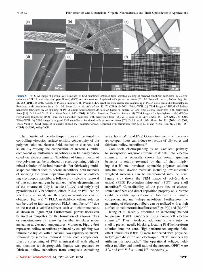
Figure 9. (a) SEM image of porous Poly-L-lactide (PLLA) nanofibers obtained from selective etching of blended-nanofibers fabricated by electro-
spinning of PLLA and poly(vinyl pyrrolidone) (PVP) mixture solution. Reprinted with permission from [63], M. Bognitzki, et al., Polym. Eng. Sci.41, 982 (2001). © 2001, Society of Plastics Engineers. (b) Porous PLLA nanofiber obtained by electrospinning of PLLA dissolved in dichloromethane.
Reprinted with permission from [64], M. Bognitzki, et al., Adv. Mater. 13, 70 (2001). © 2001, Wiley-VCH. (c) TEM image of TiO2/PVP hollow
nanofibers fabricated by co-spinning of PVP/titanium tetraisopropoxide solution based on mineral oil and ethyl alcohol. Reprinted with permission
from [65], D. Li and Y. N. Xia, Nano Lett. 4, 933 (2004). © 2004, American Chemical Society. (d) TEM image of poly(ethylene oxide) (PEO)–
Poly(dodecylthiophene) (PDT) core–shell nanofiber. Reprinted with permission from [66], Z. C. Sun, et al., Adv. Mater. 15, 1929 (2003). © 2003,
Wiley-VCH. (e) SEM image of aligned PVP nanofibers. Reprinted with permission from [67], D. Li, et al., Adv. Mater. 16, 361 (2004). © 2004,
Wiley-VCH. (f) SEM image of uniaxially aligned PVP nanofiber arrays. Reprinted with permission from [24], D. Li and Y. Xia, Adv. Mater. 16, 1151(2004). © 2004, Wiley-VCH.
The diameter of the electrospun fiber can be tuned by
controlling viscosity, surface tension, conductivity of the
polymer solution, electric field, collection distance, and
so on. By varying the composition of materials, multi-
component or multi-shape nanofibers can be easily fabri-
cated via electrospinning. Nanofibers of binary blends of
two polymers can be produced by electrospinning with the
mixed solution of desired materials. For fabricating multi-
shape nanofibers such as porous nanofibers, both methods
of inducing the phase separation phenomena or collect-
ing electrospun nanofibers, followed by selective removal
of one component, can be utilized. After electrospinning
of the mixture of Poly-L-lactide (PLLA) and poly(vinyl
pyrrolidone) (PVP) solution, either PLLA or PVP can be
selectively removed, and then porous nanofibers can be
obtained (Fig. 9(a)).63 PLLA in dichloromethane solution
can be used to fabricate porous PLLA nanofibers,24�64 due
to the use of a volatile solvent such as dichloromethane,
as shown in Figure 9(b). Furthermore, porous fibers can
be used as templates for the formation of various tubes
or nanostructures by removing the fiber templates under
annealing at elevated temperatures. Moreover, Figure 9(c)
represents hollow nanofibers produced by co-spinning two
immiscible liquids with a coaxial, two-capillary spinneret,
followed by selective removal of the core components.
Electro co-spinning of PVP in mineral oil with ethanol
and titanium tetraisopropoxide liquids was prepared to
fabricate hollow nanofibers from composite containing
amorphous TiO2 and PVP. Octane treatments on the elec-
tro co-spun fibers can induce extraction of oily cores and
fabricate hollow nanofibers.65
Core–shell electrospinning is an excellent pathway
to incorporate organo-electronic materials into electro-
spinning. It is generally known that overall spinning
behavior is totally governed by that of shell, imply-
ing that if one introduces spinnable polymer solution
into the shell, diverse materials including low-molecular
weighted materials can be incorporated into the core.
Figure 9(d) shows the TEM image of poly(ethylene
oxide) (PEO)–Poly(dodecylthiophene) (PDT) core–shell
nanofiber.66 Controllability of the pore size of electro-
spun nanofibers and direct deposition property on substrate
enable versatile applications in fabrication of multi-
component and multi-shape nanofibers. Furthermore, the
patterning of electrospun fibers can be realized with a high
surface-to-volume ratio in afilmstate (Figs. 9(e) and (f)).24�67
Jeong et al. recently described an interesting method
to prepare P3HT nanofibers using core–shell electro-
spinning.68 They introduced additional solvent into the
shell to prevent needle blocking, locating P3HT/chloroform
solution into the core. High-performance organic field-
effect transistors (OFETs) were fabricated with polyelec-
trolyte gate dielectric and electrospun P3HT nanofibers by
utilizing this approach.69 The operational voltage, field-
effect mobility and on/off ratio of the prepared OFET were
2 V, ∼ 2 cm2 V−1 s−1, and 105, respectively.
J. Nanosci. Nanotechnol. 14, 1282–1302, 2014 1291
Fabrication of One-Dimensional Organic Nanomaterials and Their Optoelectronic Applications Yu et al.
Beyond core–shell electrospinning, a polymeric blend
or composite of conducting polymer has been adopted
to produce 1D conducting polymer nanomaterials using
electrospinning. Jeong and co-workers have reported on
the fabrication of nanofibers with poly(�-caprolactone)(PCL)/P3HT blend.68 After selective dissolution of the
PCL contents on blended nanofibers, an aligned surface
morphology of P3HT could be obtained, because of the
shear stress of P3HT during electrospinning. They sug-
gested that fine nanofibers composed of P3HT can be pre-
pared by adequate control of the shear stress. Srivastava
et al. has reported on the preparation of nanofibers of
PVP and their composites with PPy.70 They employed a
multi-spinnerette electrospinning device using microchan-
nels cast in polydimethylsiloxane (PDMS) for scale-up.
The pyrrole monomer and initiator for polymerization
were introduced onto PVP solution. The insoluble PPy
compartments were well-dispersed into a PVP solution,
resulting in PPy/PVP composite nanofibers.
Yoon et al. has reported on the electrospinning of
nanofibers with polymer blend containing diacetylene
molecules.71–73 The diacetylene incorporated into poly-
mer nanofibers could be polymerized by UV irradiation
in the matrix. By utilizing the end functional groups
of diacetylene, diverse types of poly(diacetylene) elec-
trospun nanofibers could be prepared. Because these
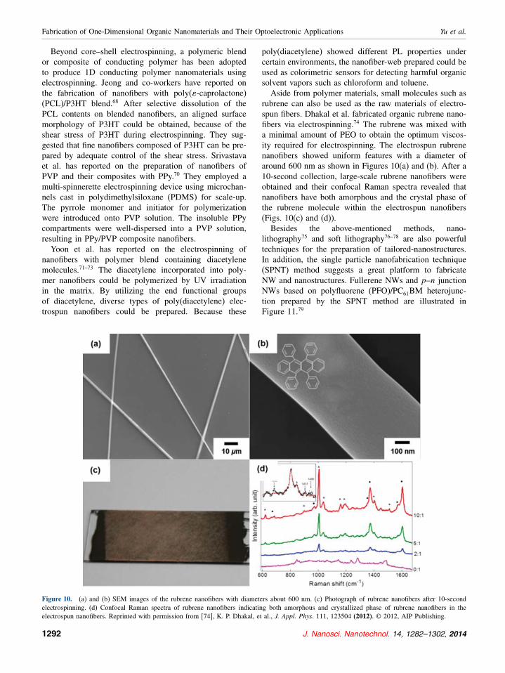
Figure 10. (a) and (b) SEM images of the rubrene nanofibers with diameters about 600 nm. (c) Photograph of rubrene nanofibers after 10-second
electrospinning. (d) Confocal Raman spectra of rubrene nanofibers indicating both amorphous and crystallized phase of rubrene nanofibers in the
electrospun nanofibers. Reprinted with permission from [74], K. P. Dhakal, et al., J. Appl. Phys. 111, 123504 (2012). © 2012, AIP Publishing.
poly(diacetylene) showed different PL properties under
certain environments, the nanofiber-web prepared could be
used as colorimetric sensors for detecting harmful organic
solvent vapors such as chloroform and toluene.
Aside from polymer materials, small molecules such as
rubrene can also be used as the raw materials of electro-
spun fibers. Dhakal et al. fabricated organic rubrene nano-
fibers via electrospinning.74 The rubrene was mixed with
a minimal amount of PEO to obtain the optimum viscos-
ity required for electrospinning. The electrospun rubrene
nanofibers showed uniform features with a diameter of
around 600 nm as shown in Figures 10(a) and (b). After a
10-second collection, large-scale rubrene nanofibers were
obtained and their confocal Raman spectra revealed that
nanofibers have both amorphous and the crystal phase of
the rubrene molecule within the electrospun nanofibers
(Figs. 10(c) and (d)).
Besides the above-mentioned methods, nano-
lithography75 and soft lithography76–78 are also powerful
techniques for the preparation of tailored-nanostructures.
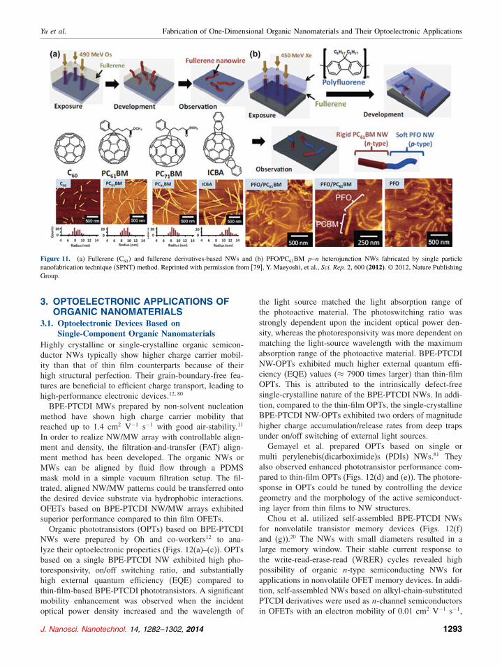
In addition, the single particle nanofabrication technique
(SPNT) method suggests a great platform to fabricate
NW and nanostructures. Fullerene NWs and p–n junction
NWs based on polyfluorene (PFO)/PC61BM heterojunc-
tion prepared by the SPNT method are illustrated in
Figure 11.79
1292 J. Nanosci. Nanotechnol. 14, 1282–1302, 2014
Yu et al. Fabrication of One-Dimensional Organic Nanomaterials and Their Optoelectronic Applications
Figure 11. (a) Fullerene (C60� and fullerene derivatives-based NWs and (b) PFO/PC61BM p–n heterojunction NWs fabricated by single particle
nanofabrication technique (SPNT) method. Reprinted with permission from [79], Y. Maeyoshi, et al., Sci. Rep. 2, 600 (2012). © 2012, Nature Publishing
Group.
3. OPTOELECTRONIC APPLICATIONS OFORGANIC NANOMATERIALS
3.1. Optoelectronic Devices Based onSingle-Component Organic Nanomaterials
Highly crystalline or single-crystalline organic semicon-
ductor NWs typically show higher charge carrier mobil-
ity than that of thin film counterparts because of their
high structural perfection. Their grain-boundary-free fea-
tures are beneficial to efficient charge transport, leading to
high-performance electronic devices.12�80
BPE-PTCDI MWs prepared by non-solvent nucleation
method have shown high charge carrier mobility that
reached up to 1.4 cm2 V−1 s−1 with good air-stability.11
In order to realize NW/MW array with controllable align-
ment and density, the filtration-and-transfer (FAT) align-
ment method has been developed. The organic NWs or
MWs can be aligned by fluid flow through a PDMS
mask mold in a simple vacuum filtration setup. The fil-
trated, aligned NW/MW patterns could be transferred onto
the desired device substrate via hydrophobic interactions.
OFETs based on BPE-PTCDI NW/MW arrays exhibited
superior performance compared to thin film OFETs.
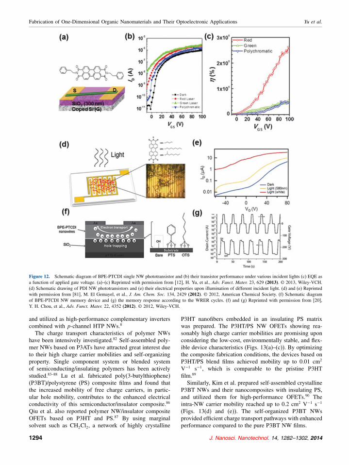
Organic phototransistors (OPTs) based on BPE-PTCDI
NWs were prepared by Oh and co-workers12 to ana-
lyze their optoelectronic properties (Figs. 12(a)–(c)). OPTs
based on a single BPE-PTCDI NW exhibited high pho-
toresponsivity, on/off switching ratio, and substantially
high external quantum efficiency (EQE) compared to
thin-film-based BPE-PTCDI phototransistors. A significant
mobility enhancement was observed when the incident
optical power density increased and the wavelength of
the light source matched the light absorption range of
the photoactive material. The photoswitching ratio was
strongly dependent upon the incident optical power den-
sity, whereas the photoresponsivity was more dependent on
matching the light-source wavelength with the maximum
absorption range of the photoactive material. BPE-PTCDI
NW-OPTs exhibited much higher external quantum effi-
ciency (EQE) values (≈ 7900 times larger) than thin-film
OPTs. This is attributed to the intrinsically defect-free
single-crystalline nature of the BPE-PTCDI NWs. In addi-
tion, compared to the thin-film OPTs, the single-crystalline
BPE-PTCDI NW-OPTs exhibited two orders of magnitude
higher charge accumulation/release rates from deep traps
under on/off switching of external light sources.
Gemayel et al. prepared OPTs based on single or
multi perylenebis(dicarboximide)s (PDIs) NWs.81 They
also observed enhanced phototransistor performance com-
pared to thin-film OPTs (Figs. 12(d) and (e)). The photore-
sponse in OPTs could be tuned by controlling the device
geometry and the morphology of the active semiconduct-
ing layer from thin films to NW structures.
Chou et al. utilized self-assembled BPE-PTCDI NWs
for nonvolatile transistor memory devices (Figs. 12(f)
and (g)).20 The NWs with small diameters resulted in a
large memory window. Their stable current response to
the write-read-erase-read (WRER) cycles revealed high
possibility of organic n-type semiconducting NWs for
applications in nonvolatile OFET memory devices. In addi-
tion, self-assembled NWs based on alkyl-chain-substituted
PTCDI derivatives were used as n-channel semiconductors
in OFETs with an electron mobility of 0.01 cm2 V−1 s−1,
J. Nanosci. Nanotechnol. 14, 1282–1302, 2014 1293
Fabrication of One-Dimensional Organic Nanomaterials and Their Optoelectronic Applications Yu et al.
Figure 12. Schematic diagram of BPE-PTCDI single NW phototransistor and (b) their transistor performance under various incident lights (c) EQE as
a function of applied gate voltage. (a)–(c) Reprinted with permission from [12], H. Yu, et al., Adv. Funct. Mater. 23, 629 (2013). © 2013, Wiley-VCH.
(d) Schematic drawing of PDI NW phototransistors and (e) their electrical properties upon illumination of different incident light. (d) and (e) Reprinted
with permission from [81], M. El Gemayel, et al., J. Am. Chem. Soc. 134, 2429 (2012). © 2012, American Chemical Society. (f) Schematic diagram
of BPE-PTCDI NW memory device and (g) the memory response according to the WRER cycles. (f) and (g) Reprinted with permission from [20],
Y. H. Chou, et al., Adv. Funct. Mater. 22, 4352 (2012). © 2012, Wiley-VCH.
and utilized as high-performance complementary inverters
combined with p-channel HTP NWs.8
The charge transport characteristics of polymer NWs
have been intensively investigated.82 Self-assembled poly-
mer NWs based on P3ATs have attracted great interest due
to their high charge carrier mobilities and self-organizing
property. Single component system or blended system
of semiconducting/insulating polymers has been actively
studied.83–88 Lu et al. fabricated poly(3-butylthiophene)
(P3BT)/polystyrene (PS) composite films and found that
the increased mobility of free charge carriers, in partic-
ular hole mobility, contributes to the enhanced electrical
conductivity of this semiconductor/insulator composite.86
Qiu et al. also reported polymer NW/insulator composite
OFETs based on P3HT and PS.87 By using marginal
solvent such as CH2Cl2, a network of highly crystalline
P3HT nanofibers embedded in an insulating PS matrix
was prepared. The P3HT/PS NW OFETs showing rea-
sonably high charge carrier mobilities are promising upon
considering the low-cost, environmentally stable, and flex-
ible device characteristics (Figs. 13(a)–(c)). By optimizing
the composite fabrication conditions, the devices based on
P3HT/PS blend films achieved mobility up to 0.01 cm2
V−1 s−1, which is comparable to the pristine P3HT
film.89
Similarly, Kim et al. prepared self-assembled crystalline
P3BT NWs and their nanocomposites with insulating PS,
and utilized them for high-performance OFETs.90 The
intra-NW carrier mobility reached up to 0.2 cm2 V−1 s−1
(Figs. 13(d) and (e)). The self-organized P3BT NWs
provided efficient charge transport pathways with enhanced
performance compared to the pure P3BT NW films.
1294 J. Nanosci. Nanotechnol. 14, 1282–1302, 2014
Yu et al. Fabrication of One-Dimensional Organic Nanomaterials and Their Optoelectronic Applications
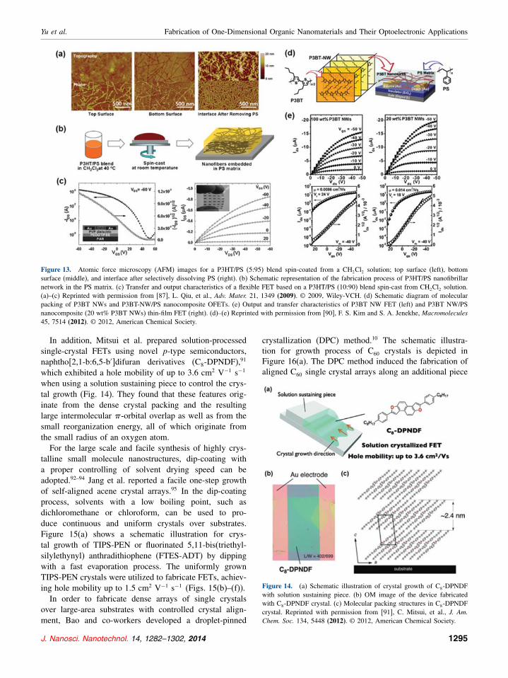
Figure 13. Atomic force microscopy (AFM) images for a P3HT/PS (5:95) blend spin-coated from a CH2Cl2 solution; top surface (left), bottom
surface (middle), and interface after selectively dissolving PS (right). (b) Schematic representation of the fabrication process of P3HT/PS nanofibrillar
network in the PS matrix. (c) Transfer and output characteristics of a flexible FET based on a P3HT/PS (10:90) blend spin-cast from CH2Cl2 solution.
(a)–(c) Reprinted with permission from [87], L. Qiu, et al., Adv. Mater. 21, 1349 (2009). © 2009, Wiley-VCH. (d) Schematic diagram of molecular
packing of P3BT NWs and P3BT-NW/PS nanocomposite OFETs. (e) Output and transfer characteristics of P3BT NW FET (left) and P3BT NW/PS
nanocomposite (20 wt% P3BT NWs) thin-film FET (right). (d)–(e) Reprinted with permission from [90], F. S. Kim and S. A. Jenekhe, Macromolecules45, 7514 (2012). © 2012, American Chemical Society.
In addition, Mitsui et al. prepared solution-processed
single-crystal FETs using novel p-type semiconductors,
naphtho[2,1-b:6,5-b′]difuran derivatives (C8-DPNDF),91
which exhibited a hole mobility of up to 3.6 cm2 V−1 s−1
when using a solution sustaining piece to control the crys-
tal growth (Fig. 14). They found that these features orig-
inate from the dense crystal packing and the resulting
large intermolecular �-orbital overlap as well as from the
small reorganization energy, all of which originate from
the small radius of an oxygen atom.
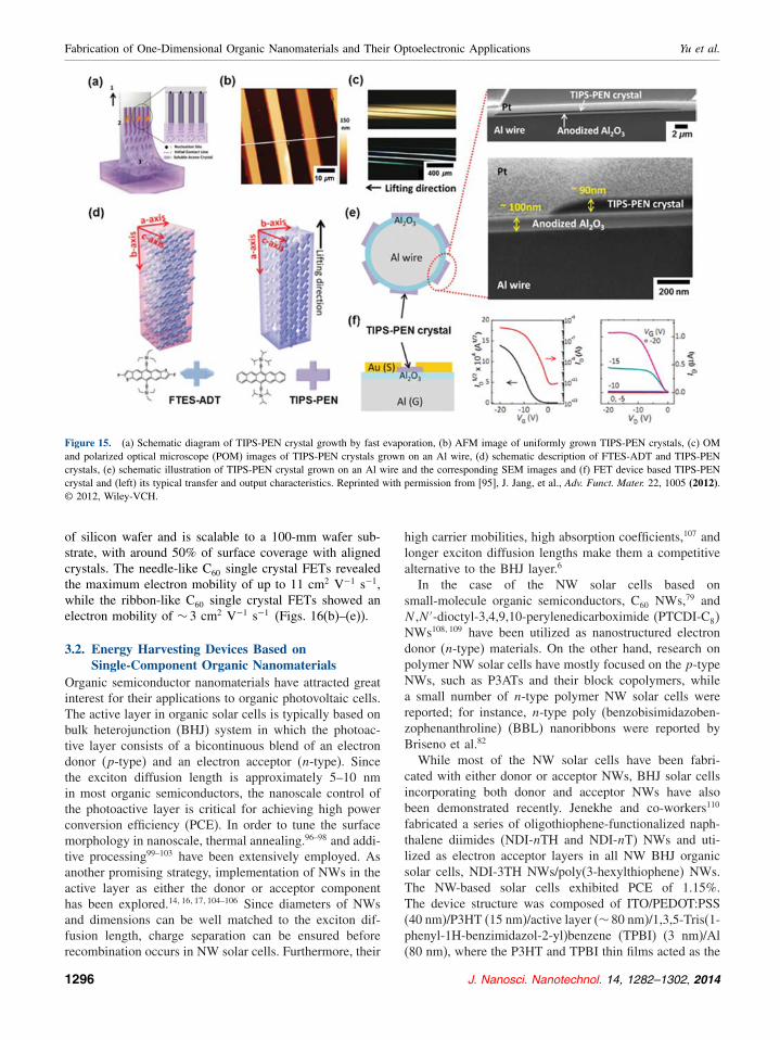
For the large scale and facile synthesis of highly crys-
talline small molecule nanostructures, dip-coating with
a proper controlling of solvent drying speed can be
adopted.92–94 Jang et al. reported a facile one-step growth
of self-aligned acene crystal arrays.95 In the dip-coating
process, solvents with a low boiling point, such as
dichloromethane or chloroform, can be used to pro-
duce continuous and uniform crystals over substrates.
Figure 15(a) shows a schematic illustration for crys-
tal growth of TIPS-PEN or fluorinated 5,11-bis(triethyl-
silylethynyl) anthradithiophene (FTES-ADT) by dipping
with a fast evaporation process. The uniformly grown
TIPS-PEN crystals were utilized to fabricate FETs, achiev-
ing hole mobility up to 1.5 cm2 V−1 s−1 (Figs. 15(b)–(f)).
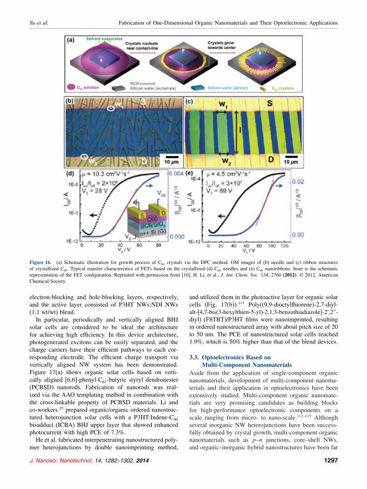
In order to fabricate dense arrays of single crystals
over large-area substrates with controlled crystal align-
ment, Bao and co-workers developed a droplet-pinned
crystallization (DPC) method.10 The schematic illustra-
tion for growth process of C60 crystals is depicted in
Figure 16(a). The DPC method induced the fabrication of
aligned C60 single crystal arrays along an additional piece
Figure 14. (a) Schematic illustration of crystal growth of C8-DPNDF
with solution sustaining piece. (b) OM image of the device fabricated
with C8-DPNDF crystal. (c) Molecular packing structures in C8-DPNDF
crystal. Reprinted with permission from [91], C. Mitsui, et al., J. Am.Chem. Soc. 134, 5448 (2012). © 2012, American Chemical Society.
J. Nanosci. Nanotechnol. 14, 1282–1302, 2014 1295
Fabrication of One-Dimensional Organic Nanomaterials and Their Optoelectronic Applications Yu et al.
Figure 15. (a) Schematic diagram of TIPS-PEN crystal growth by fast evaporation, (b) AFM image of uniformly grown TIPS-PEN crystals, (c) OM
and polarized optical microscope (POM) images of TIPS-PEN crystals grown on an Al wire, (d) schematic description of FTES-ADT and TIPS-PEN
crystals, (e) schematic illustration of TIPS-PEN crystal grown on an Al wire and the corresponding SEM images and (f) FET device based TIPS-PEN
crystal and (left) its typical transfer and output characteristics. Reprinted with permission from [95], J. Jang, et al., Adv. Funct. Mater. 22, 1005 (2012).© 2012, Wiley-VCH.
of silicon wafer and is scalable to a 100-mm wafer sub-
strate, with around 50% of surface coverage with aligned
crystals. The needle-like C60 single crystal FETs revealed
the maximum electron mobility of up to 11 cm2 V−1 s−1,
while the ribbon-like C60 single crystal FETs showed an
electron mobility of ∼ 3 cm2 V−1 s−1 (Figs. 16(b)–(e)).
3.2. Energy Harvesting Devices Based onSingle-Component Organic Nanomaterials
Organic semiconductor nanomaterials have attracted great
interest for their applications to organic photovoltaic cells.
The active layer in organic solar cells is typically based on
bulk heterojunction (BHJ) system in which the photoac-
tive layer consists of a bicontinuous blend of an electron
donor (p-type) and an electron acceptor (n-type). Sincethe exciton diffusion length is approximately 5–10 nm
in most organic semiconductors, the nanoscale control of
the photoactive layer is critical for achieving high power
conversion efficiency (PCE). In order to tune the surface
morphology in nanoscale, thermal annealing.96–98 and addi-
tive processing99–103 have been extensively employed. As
another promising strategy, implementation of NWs in the
active layer as either the donor or acceptor component
has been explored.14�16�17�104–106 Since diameters of NWs
and dimensions can be well matched to the exciton dif-
fusion length, charge separation can be ensured before
recombination occurs in NW solar cells. Furthermore, their
high carrier mobilities, high absorption coefficients,107 and
longer exciton diffusion lengths make them a competitive
alternative to the BHJ layer.6
In the case of the NW solar cells based on
small-molecule organic semiconductors, C60 NWs,79 and
N ,N ′-dioctyl-3,4,9,10-perylenedicarboximide (PTCDI-C8�NWs108�109 have been utilized as nanostructured electron
donor (n-type) materials. On the other hand, research on
polymer NW solar cells have mostly focused on the p-typeNWs, such as P3ATs and their block copolymers, while
a small number of n-type polymer NW solar cells were
reported; for instance, n-type poly (benzobisimidazoben-
zophenanthroline) (BBL) nanoribbons were reported by
Briseno et al.82
While most of the NW solar cells have been fabri-
cated with either donor or acceptor NWs, BHJ solar cells
incorporating both donor and acceptor NWs have also
been demonstrated recently. Jenekhe and co-workers110
fabricated a series of oligothiophene-functionalized naph-
thalene diimides (NDI-nTH and NDI-nT) NWs and uti-
lized as electron acceptor layers in all NW BHJ organic
solar cells, NDI-3TH NWs/poly(3-hexylthiophene) NWs.
The NW-based solar cells exhibited PCE of 1.15%.
The device structure was composed of ITO/PEDOT:PSS
(40 nm)/P3HT (15 nm)/active layer (∼ 80 nm)/1,3,5-Tris(1-
phenyl-1H-benzimidazol-2-yl)benzene (TPBI) (3 nm)/Al
(80 nm), where the P3HT and TPBI thin films acted as the
1296 J. Nanosci. Nanotechnol. 14, 1282–1302, 2014
Yu et al. Fabrication of One-Dimensional Organic Nanomaterials and Their Optoelectronic Applications
Figure 16. (a) Schematic illustration for growth process of C60 crystals via the DPC method. OM images of (b) needle and (c) ribbon structures
of crystallized C60. Typical transfer characteristics of FETs based on the crystallized (d) C60 needles and (e) C60 nanoribbons. Inset is the schematic
representation of the FET configuration. Reprinted with permission from [10], H. Li, et al., J. Am. Chem. Soc. 134, 2760 (2012). © 2012, American
Chemical Society.
electron-blocking and hole-blocking layers, respectively,
and the active layer consisted of P3HT NWs:NDI NWs
(1:1 wt/wt) blend.
In particular, periodically and vertically aligned BHJ
solar cells are considered to be ideal the architecture
for achieving high efficiency. In this device architecture,
photogenerated excitons can be easily separated, and the
charge carriers have their efficient pathways to each cor-
responding electrode. The efficient charge transport via
vertically aligned NW system has been demonstrated.
Figure 17(a) shows organic solar cells based on verti-
cally aligned [6,6]-phenyl-C61-butyric styryl dendronester
(PCBSD) nanorods. Fabrication of nanorods was real-
ized via the AAO templating method in combination with
the cross-linkable property of PCBSD materials. Li and
co-workers.15 prepared organic/organic ordered nanostruc-
tured heterojunction solar cells with a P3HT:Indene-C60
bisadduct (ICBA) BHJ upper layer that showed enhanced
photocurrent with high PCE of 7.3%.
He et al. fabricated interpenetrating nanostructured poly-
mer heterojunctions by double nanoimprinting method,
and utilized them in the photoactive layer for organic solar
cells (Fig. 17(b)).111 Poly((9,9-dioctylfluorene)-2,7-diyl-
alt-[4,7-bis(3-hexylthien-5-yl)-2,1,3-benzothiadiazole]-2′,2′′-diyl) (F8TBT)/P3HT films were nanoimprinted, resulting
in ordered nanostructured array with about pitch size of 20
to 50 nm. The PCE of nanostructured solar cells reached
1.9%, which is 50% higher than that of the blend devices.
3.3. Optoelectronics Based onMulti-Component Nanomaterials
Aside from the application of single-component organic
nanomaterials, development of multi-component nanoma-
terials and their application in optoelectronics have been
extensively studied. Multi-component organic nanomate-
rials are very promising candidates as building blocks
for high-performance optoelectronic components on a
scale ranging from micro- to nano-scale.112–115 Although
several inorganic NW heterojunctions have been success-
fully obtained by crystal growth, multi-component organic
nanomaterials such as p–n junctions, core–shell NWs,
and organic–inorganic hybrid nanostructures have been far
J. Nanosci. Nanotechnol. 14, 1282–1302, 2014 1297
Fabrication of One-Dimensional Organic Nanomaterials and Their Optoelectronic Applications Yu et al.
Figure 17. (a) Illustration of organic solar cells fabricated by cross-linked PCBSD nanostructures as active layers (left) and its photovoltaic per-
formance. Reprinted with permission from [15], C. Y. Chang, et al., Angew. Chem., Int. Ed. 50, 9386 (2011). © 2011, Wiley-VCH. (b) Schematic
diagram of aligned NW F8TBT/P3HT organic solar cells prepared by imprinting method (left) and the corresponding SEM image (right). Reprinted
with permission from [111], X. He, et al., Nano Lett. 10, 1302 (2010). © 2010, American Chemical Society.
less developed and incorporated into nanoscale photonic
devices.116–118 Assembling organic NWs into complex
heterostructures is critical for realizing multi-functional
devices and understanding charge transport and energy
transfer phenomena.
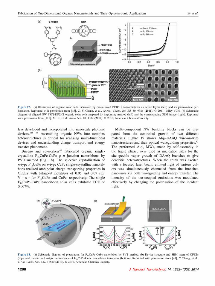
Briseno and co-workers41 fabricated organic single-
crystalline F16CuPc-CuPc p–n junction nanoribbons by
PVD method (Fig. 18). The selective crystallization of
n-type F16CuPc on p-type CuPc single-crystalline nanorib-bons realized ambipolar charge transporting properties in
OFETs with balanced mobilities of 0.05 and 0.07 cm2
V−1 s−1 for F16CuPc and CuPc, respectively. The single
F16CuPc-CuPc nanoribbon solar cells exhibited PCE of
0.007%.
Figure 18. (a) Schematic diagram of preparation for F16CuPc-CuPc nanoribbon by PVT method. (b) Device structure and SEM mage of OFETs
(top), and transfer and output performance of F16CuPc-CuPc nanoribbon transistors (bottom). Reprinted with permission from [41], Y. Zhang, et al.,
J. Am. Chem. Soc. 132, 11580 (2010). © 2010, American Chemical Society.
Multi-component NW building blocks can be pre-
pared from the controlled growth of two different
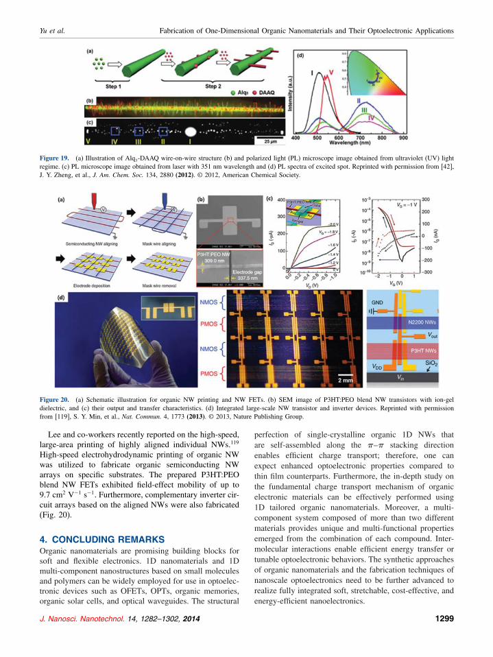
materials. Figure 19 shows Alq3-DAAQ wire-on-wire
nanostructures and their optical waveguiding properties.42
The preformed Alq3 MWs, made by self-assembly in
the liquid phase, were used as nucleation sites for the
site-specific vapor growth of DAAQ branches to give
dendritic heterostructures. When the trunk was excited
with a focused laser beam, emitted light of various col-
ors was simultaneously channeled from the branched
nanowires via both waveguiding and energy transfer. The
intensity of the out-coupled emissions was modulated
effectively by changing the polarization of the incident
light.
1298 J. Nanosci. Nanotechnol. 14, 1282–1302, 2014
Yu et al. Fabrication of One-Dimensional Organic Nanomaterials and Their Optoelectronic Applications
Figure 19. (a) Illustration of Alq3-DAAQ wire-on-wire structure (b) and polarized light (PL) microscope image obtained from ultraviolet (UV) light
regime. (c) PL microscope image obtained from laser with 351 nm wavelength and (d) PL spectra of excited spot. Reprinted with permission from [42],
J. Y. Zheng, et al., J. Am. Chem. Soc. 134, 2880 (2012). © 2012, American Chemical Society.
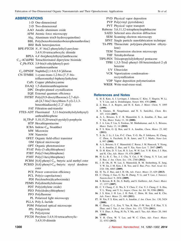
Figure 20. (a) Schematic illustration for organic NW printing and NW FETs. (b) SEM image of P3HT:PEO blend NW transistors with ion-gel
dielectric, and (c) their output and transfer characteristics. (d) Integrated large-scale NW transistor and inverter devices. Reprinted with permission
from [119], S. Y. Min, et al., Nat. Commun. 4, 1773 (2013). © 2013, Nature Publishing Group.
Lee and co-workers recently reported on the high-speed,
large-area printing of highly aligned individual NWs.119
High-speed electrohydrodynamic printing of organic NW
was utilized to fabricate organic semiconducting NW
arrays on specific substrates. The prepared P3HT:PEO
blend NW FETs exhibited field-effect mobility of up to
9.7 cm2 V−1 s−1. Furthermore, complementary inverter cir-
cuit arrays based on the aligned NWs were also fabricated
(Fig. 20).
4. CONCLUDING REMARKSOrganic nanomaterials are promising building blocks for
soft and flexible electronics. 1D nanomaterials and 1D
multi-component nanostructures based on small molecules
and polymers can be widely employed for use in optoelec-
tronic devices such as OFETs, OPTs, organic memories,
organic solar cells, and optical waveguides. The structural
perfection of single-crystalline organic 1D NWs that
are self-assembled along the �–� stacking direction
enables efficient charge transport; therefore, one can
expect enhanced optoelectronic properties compared to
thin film counterparts. Furthermore, the in-depth study on
the fundamental charge transport mechanism of organic
electronic materials can be effectively performed using
1D tailored organic nanomaterials. Moreover, a multi-
component system composed of more than two different
materials provides unique and multi-functional properties
emerged from the combination of each compound. Inter-
molecular interactions enable efficient energy transfer or
tunable optoelectronic behaviors. The synthetic approaches
of organic nanomaterials and the fabrication techniques of
nanoscale optoelectronics need to be further advanced to
realize fully integrated soft, stretchable, cost-effective, and
energy-efficient nanoelectronics.
J. Nanosci. Nanotechnol. 14, 1282–1302, 2014 1299
Fabrication of One-Dimensional Organic Nanomaterials and Their Optoelectronic Applications Yu et al.
ABBREVIATIONS1-D One-dimensional
2-D Two-dimensional
AAO Anodic aluminum oxide
AFM Atomic force microscopy
Alq3 Aluminum tris(8-hydroxyquinoline)
BBL Poly(benzobisimidazobenzophenanthroline)
BHJ Bulk heterojunction
BPE-PTCDI N�N ′-bis(2-phenylethyl)-perylene-3,4:9,10-tetracarboxylic diimide
BPEA 4,4′-bis(phenylethynyl)anthraceneC12-4CldiPBI Tetrachlorinated diperylene bisimide
C2Ph-PXX 3,9-bis(4-ethylphenyl)-peri-
xanthenoxanthene
C8-DPNDF Naphtho[2,1-b:6,5-b′]difuranCN-TFMBE 1-cyano-trans-1,2-bis-(3′,5′-bis-
trifluoromethyl-biphenyl)ethylene
CuPc Copper phthalocyanine
DAAQ 1,5-diaminoanthraquinone
DPC Droplet-pinned crystallization
EQE External quantum efficiency
F8TBT Poly((9,9-dioctylfluorene)-2,7-diyl-
alt-[4,7-bis(3-hexylthien-5-yl)-2,1,3-
benzothiadiazole]-2′,2′′-diyl)FAT Filtration-and-transfer
FTES-ADT Fluorinated 5,11-bis(triethylsilylethynyl)
anthradithiophene
H2TPyP 5,10,15,20-tetra(4-pyridyl)-porphyrin
HTP Hexathiapentacene
ICBA Indene-C60 bisadduct
MW Microwire
NW Nanowire
OFET Organic field-effect transistor
OM Optical microscope
OPT Organic phototransistor
P3AT Poly-(3-alkylthiophene)
P3BT Poly(3-butylthiophene)
P3HT Poly(3-hexylthiophene)
PCBM [6,6]-phenyl C61 butyric acid methyl ester
PCBSD [6,6]-phenyl-C61-butyric styryl dendron-
ester
PCE Power conversion efficiency
PCL Poly(�-caprolactone)PDI Perylenebis(dicarboximide)
PDMS Polydimethylsiloxane
PDT Poly(ethylene oxide)
PEO Poly(dodecylthiophene)
PFO Polyfluorene
PL Polarized light microscopy
PLLA Poly-L-lactide
POM Polarized optical microscope
PPy Polypyrrole
PS Polystyrene
PTCDI Perylene-3,4,9,10-tetracarboxylic-
3,4,9,10-diimide
PVD Physical vapor deposition
PVP Poly(vinyl pyrrolidone)
PVT Physical vapor transport
Rubrene 5,6,11,12-tetraphenylnaphthacene
SAED Selected area electron diffraction
SEM Scanning electron microscopy
SPNT Single particle nanofabrication technique
TA-PPE Thioacetate poly(para-phenylene ethyny-
lene)
TEM Transmission electron microscopy
THF Tetrahydrofuran
TIPS-PEN Triisopropylsilylethynyl pentacene
TPBI 1,3,5-Tris(1-phenyl-1H-benzimidazol-2-yl)
benzene
UV Ultraviolet
VCR Vaporization–condensation–
recrystallization
VDP Vapor deposition polymerization
WRER Write-read-erase-read.
References and Notes1. H. E. Katz, A. J. Lovinger, J. Johnson, C. Kloc, T. Slegrist, W. Li,
Y. Y. Lin, and A. Dodabalapur, Nature 404, 478 (2000).2. Z. Bao, J. A. Rogers, and H. E. Katz, J. Mater. Chem. 9, 1895
(1999).3. S. Guenes, H. Neugebauer, and N. S. Sariciftci, Chem. Rev.
107, 1324 (2007).4. A. L. Briseno, S. C. B. Mannsfeld, S. A. Jenekhe, Z. Bao, and
Y. Xia, Mater. Today 11, 38 (2008).5. J. A. Lim, F. Liu, S. Ferdous, M. Muthukumar, and A. L. Briseno,
Mater. Today 13, 14 (2010).6. F. S. Kim, G. Q. Ren, and S. A. Jenekhe, Chem. Mater. 23, 682
(2011).7. S. Ju, J. Li, J. Liu, P.-C. Chen, Y.-G. Ha, F. Ishikawa, H. Chang,
C. Zhou, A. Facchetti, D. B. Janes, and T. J. Marks, Nano Lett.8, 997 (2008).
8. A. L. Briseno, S. C. Mannsfeld, C. Reese, J. M. Hancock, Y. Xiong,
S. A. Jenekhe, Z. Bao, and Y. Xia, Nano Lett. 7, 2847 (2007).9. D. H. Kim, D. Y. Lee, H. S. Lee, W. H. Lee, Y. H. Kim, J. I. Han,
and K. Cho, Adv. Mater. 19, 678 (2007).10. H. Li, B. C. Tee, J. J. Cha, Y. Cui, J. W. Chung, S. Y. Lee, and
Z. Bao, J. Am. Chem. Soc. 134, 2760 (2012).11. J. H. Oh, H. W. Lee, S. Mannsfeld, R. M. Stoltenberg, E. Jung,
Y. W. Jin, J. M. Kim, J. B. Yoo, and Z. Bao, Proc. Natl. Acad. Sci.USA 106, 6065 (2009).
12. H. Yu, Z. Bao, and J. H. Oh, Adv. Funct. Mater. 23, 629 (2013).13. C. Cheng, J. Gao, G. Xu, H. Zhang, Y. Li, and Y. Luo, J. Nanosci.
Nanotechnol. 9, 2836 (2009).14. S. Berson, B. R. De, S. Bailly, and S. Guillerez, Adv. Funct. Mater.
17, 1377 (2007).15. C. Y. Chang, C. E. Wu, S. Y. Chen, C. Cui, Y. J. Cheng, C. S. Hsu,
Y. L. Wang, and Y. Li, Angew. Chem. Int. Ed. 50, 9386 (2011).16. J. S. Kim, J. H. Lee, J. H. Park, C. Shim, M. Sim, and K. Cho,
Adv. Funct. Mater. 21, 480 (2011).17. H. Xin, F. S. Kim, and S. A. Jenekhe, J. Am. Chem. Soc. 130, 5424
(2008).18. C. Zhang, C.-L. Zou, Y. Yan, R. Hao, F.-W. Sun, Z.-F. Han, Y. S.
Zhao, and J. Yao, J. Am. Chem. Soc. 133, 7276 (2011).19. Y. S. Zhao, A. Peng, H. Fu, Y. Ma, and J. Yao, Adv. Mater. 20, 1661
(2008).20. Y. H. Chou, W. Y. Lee, and W. C. Chen, Adv. Funct. Mater.
22, 4352 (2012).
1300 J. Nanosci. Nanotechnol. 14, 1282–1302, 2014
Yu et al. Fabrication of One-Dimensional Organic Nanomaterials and Their Optoelectronic Applications
21. Y. S. Zhao, J. Wu, and J. Huang, J. Am. Chem. Soc. 131, 3158(2009).
22. B. Su, Y. Wu, and L. Jiang, Chem. Soc. Rev. 41, 7832 (2012).23. Z. Wang, R. Bao, X. Zhang, X. Ou, C.-S. Lee, J. C. Chang, and
X. Zhang, Angew. Chem., Int. Ed. 50, 2811 (2011).24. D. Li and Y. Xia, Adv. Mater. 16, 1151 (2004).25. T. Lei and J. Pei, J. Mater. Chem. 22, 785 (2012).26. B. K. An, S. H. Gihm, J. W. Chung, C. R. Park, S. K. Kwon, and
S. Y. Park, J. Am. Chem. Soc. 131, 3950 (2009).27. B. K. An, J. Gierschner, and S. Y. Park, Acc. Chem. Res. 45, 544
(2012).28. L. Zang, Y. Che, and J. S. Moore, Acc. Chem. Res. 41, 1596 (2008).29. K. Balakrishnan, A. Datar, R. Oitker, H. Chen, J. Zuo, and L. Zang,
J. Am. Chem. Soc. 127, 10496 (2005).30. A. Lv, S. R. Puniredd, J. Zhang, Z. Li, H. Zhu, W. Jiang, H. Dong,
Y. He, L. Jiang, Y. Li, W. Pisula, Q. Meng, W. Hu, and Z. Wang,
Adv. Mater. 24, 2626 (2012).31. O. Goto, S. Tomiya, Y. Murakami, A. Shinozaki, A. Toda,
J. Kasahara, and D. Hobara, Adv. Mater. 24, 1117 (2012).32. K. J. Ihn, J. Moulton, and P. Smith, J. Polym. Sci., Part B: Polym.
Phys. 31, 735 (1993).33. N. Kiriy, E. Jaehne, H.-J. Adler, M. Schneider, A. Kiriy,
G. Gorodyska, S. Minko, D. Jehnichen, P. Simon, A. A. Fokin, and
M. Stamm, Nano Lett. 3, 707 (2003).34. D. H. Kim, J. T. Han, Y. D. Park, Y. Jang, J. H. Cho, M. Hwang,
and K. Cho, Adv. Mater. 18, 719 (2006).35. H. Dong, S. Jiang, L. Jiang, Y. Liu, H. Li, W. Hu, E. Wang, S. Yan,
Z. Wei, W. Xu, and X. Gong, J. Am. Chem. Soc. 131, 17315 (2009).36. T. Thurakitseree, E. Einarsson, R. Xiang, P. Zhao, S. Aikawa,
S. Chiashi, J. Shiomi, and S. Maruyama, J. Nanosci. Nanotechnol.12, 370 (2012).
37. N. T. Q. Hoa, H.-H. Heo, J.-K. Lim, G.-M. Kim, and E.-T. Kim,
J. Nanosci. Nanotechnol. 12, 1411 (2012).38. Y.-B. Chung, S.-H. Lee, S.-H. Bae, H.-K. Park, J.-S. Jung, and
N.-M. Hwang, J. Nanosci. Nanotechnol. 12, 5947 (2012).39. Y. S. Zhao, P. Zhan, J. Kim, C. Sun, and J. Huang, ACS Nano
4, 1630 (2010).40. Q. H. Cui, L. Jiang, C. Zhang, Y. S. Zhao, W. Hu, and J. Yao, Adv.
Mater. 24, 2332 (2012).41. Y. Zhang, H. Dong, Q. Tang, S. Ferdous, F. Liu, S. C. Mannsfeld,
W. Hu, and A. L. Briseno, J. Am. Chem. Soc. 132, 11580 (2010).42. J. Y. Zheng, Y. Yan, X. Wang, Y. S. Zhao, J. Huang, and J. Yao,
J. Am. Chem. Soc. 134, 2880 (2012).43. Y. Yan, C. Zhang, J. Y. Zheng, J. Yao, and Y. S. Zhao, Adv. Mater.
24, 5681 (2012).44. J. E. Park, M. Son, M. Hong, G. Lee, and H. C. Choi, Angew.
Chem., Int. Ed. 51, 6383 (2012).45. C. G. Wu and T. Bein, Science 264, 1757 (1994).46. T. Q. Nguyen, J. Wu, V. V. Doan, B. J. Schwartz, and S. H. Tolbert,
Science 288, 652 (2000).47. B. Cao, M. Ji, and S. Sun, J. Nanosci. Nanotechnol. 13, 5827
(2013).48. J. Jang and J. H. Oh, Chem. Commun. 882 (2004).49. K. J. Lee, J. H. Oh, Y. Kim, and J. Jang, Chem. Mater. 18, 5002
(2006).50. J.-K. Lee, W.-K. Koh, W.-S. Chae, and Y.-R. Kim, Chem. Commun.
138 (2002).51. J. I. Lee, S. H. Cho, S. M. Park, J. K. Kim, J. W. Yu, Y. C. Kim,
and T. P. Russell, Nano Lett. 8, 2315 (2008).52. H. Yoon, M. Chang, and J. Jang, Adv. Funct. Mater. 17, 431 (2007).53. K. Akagi, G. Piao, S. Kaneko, K. Sakamaki, H. Shirakawa, and
M. Kyotani, Science 282, 1683 (1998).54. T. Kato, Science 295, 2414 (2002).55. J. R. Capadona, O. Van Den Berg, L. A. Capadona, M. Schroeter,
S. J. Rowan, D. J. Tyler, and C. Weder, Nat. Nanotechnol. 2, 765(2007).
56. K. M. Alam, A. P. Singh, R. Starko-Bowes, S. C. Bodepudi, and
S. Pramanik, Adv. Funct. Mater. 22, 3298 (2012).57. J. F. Cooley, Apparatus for electrically dispersing fluids, U.S. Patent
692,631, Feburary (1902).58. W. J. Morton, Method of dispersing fluids, U.S. Patent 705,691,
July (1902).59. K. Hagiwaba, O. Oji-Machi, and K. Ku, Process for manufacturing
artificial silk and other filaments by applying electric current, U.S.
Patent 1,699,615, January (1929).60. D. H. Reneker and A. L. Yarin, Polymer 49, 2387 (2008).61. C. Chang, V. H. Tran, J. Wang, Y.-K. Fuh, and L. Lin, Nano Lett.
10, 726 (2010).62. F. Di Benedetto, A. Camposeo, S. Pagliara, E. Mele, L. Persano,
R. Stabile, R. Cingolani, and D. Pisignano, Nat. Nanotechnol.3, 614 (2008).
63. M. Bognitzki, T. Frese, M. Steinhart, A. Greiner, J. H. Wendorff,
A. Schaper, and M. Hellwig, Polym. Eng. Sci. 41, 982 (2001).64. M. Bognitzki, W. Czado, T. Frese, A. Schaper, M. Hellwig,
M. Steinhart, A. Greiner, and J. H. Wendorff, Adv. Mater. 13, 70(2001).
65. D. Li and Y. N. Xia, Nano Lett. 4, 933 (2004).66. Z. C. Sun, E. Zussman, A. L. Yarin, J. H. Wendorff, and A. Greiner,
Adv. Mater. 15, 1929 (2003).67. D. Li, Y. Wang, and Y. Xia, Adv. Mater. 16, 361 (2004).68. S. Lee, G. D. Moon, and U. Jeong, J. Mater. Chem. 19, 743 (2009).69. S. W. Lee, H. J. Lee, J. H. Choi, W. G. Koh, J. M. Myoung, J. H.
Hur, J. J. Park, J. H. Cho, and U. Jeong, Nano Lett. 10, 347 (2009).70. Y. Srivastava, M. Marquez, and T. Thorsen, J. Appl. Polym. Sci.
106, 3171 (2007).71. J. Yoon, Y.-S. Jung, and J.-M. Kim, Adv. Funct. Mater. 19, 209
(2009).72. J. Yoon and J.-M. Kim, Macromol. Chem. Phys. 209, 2194 (2008).73. J. Yoon, S. K. Chae, and J.-M. Kim, J. Am. Chem. Soc. 129, 3038
(2007).74. K. P. Dhakal, H. Lee, L. J. Woo, J. Joo, M. Guthold, and J. Kim,
J. Appl. Phys. 111, 123504 (2012).75. J. H. Lim and C. A. Mirkin, Adv. Mater. 14, 1474 (2002).76. M. Aryal, K. Trivedi, and W. W. Hu, ACS Nano 3, 3085 (2009).77. Z. Zheng, K. H. Yim, M. S. Saifullah, M. E. Welland, R. H. Friend,
J. S. Kim, and W. T. Huck, Nano Lett. 7, 987 (2007).78. Z. Hu, B. Muls, L. Gence, D. A. Serban, J. Hofkens, S. Melinte,
B. Nysten, S. Demoustier-Champagne, and A. M. Jonas, Nano Lett.7, 3639 (2007).
79. Y. Maeyoshi, A. Saeki, S. Suwa, M. Omichi, H. Marui, A. Asano,
S. Tsukuda, M. Sugimoto, A. Kishimura, K. Kataoka, and S. Seki,
Sci. Rep. 2, 600 (2012).80. K. S. Park, S. M. Salunkhe, I. Lim, C.-G. Cho, S.-H. Han, and
M. M. Sung, Adv. Mater. 25, 3351 (2013).81. M. El Gemayel, M. Treier, C. Musumeci, C. Li, K. Mullen, and
P. Samori, J. Am. Chem. Soc. 134, 2429 (2012).82. A. L. Briseno, S. C. B. Mannsfeld, P. J. Shamberger, F. S. Ohuchi,
Z. Bao, S. A. Jenekhe, and Y. Xia, Chem. Mater. 20, 4712 (2008).83. T. A. M. Ferenczi, C. Müller, D. D. C. Bradley, P. Smith, J. Nelson,
and N. Stingelin, Adv. Mater. 23, 4093 (2011).84. J. A. Lim, J.-H. Kim, L. Qiu, W. H. Lee, H. S. Lee, D. Kwak, and
K. Cho, Adv. Funct. Mater. 20, 3292 (2010).85. F. Yakuphanoglu, Synth. Met. 160, 1551 (2010).86. G. Lu, H. Tang, Y. Huan, S. Li, L. Li, Y. Wang, and X. Yang, Adv.
Funct. Mater. 20, 1714 (2010).87. L. Qiu, W. H. Lee, X. Wang, J. S. Kim, J. A. Lim, D. Kwak, S. Lee,
and K. Cho, Adv. Mater. 21, 1349 (2009).88. D. T. James, B. K. C. Kjellander, W. T. T. Smaal, G. H. Gelinck,
C. Combe, I. McCulloch, R. Wilson, J. H. Burroughes, D. D.
C. Bradley, and J.-S. Kim, ACS Nano 5, 9824 (2011).89. L. Qiu, X. Wang, W. H. Lee, J. A. Lim, J. S. Kim, D. Kwak, and
K. Cho, Chem. Mater. 21, 4380 (2009).
J. Nanosci. Nanotechnol. 14, 1282–1302, 2014 1301

Fabrication of One-Dimensional Organic Nanomaterials and Their Optoelectronic Applications Yu et al.
90. F. S. Kim and S. A. Jenekhe, Macromolecules 45, 7514 (2012).91. C. Mitsui, J. Soeda, K. Miwa, H. Tsuji, J. Takeya, and
E. Nakamura, J. Am. Chem. Soc. 134, 5448 (2012).92. S. Nam, J. Jang, J. E. Anthony, J.-J. Park, C. E. Park, and K. Kim,
ACS Appl. Mater. Interfaces 5, 2146 (2013).93. Y. Wu, B. Bao, B. Su, and L. Jiang, J. Mater. Chem. A 1, 8581
(2013).94. K. Ali, U. Pietsch, and S. Grigorian, J. Appl. Crystallogr. 46, 908
(2013).95. J. Jang, S. Nam, K. Im, J. Hur, S. N. Cha, J. Kim, H. B. Son,
H. Suh, M. A. Loth, J. E. Anthony, J.-J. Park, C. E. Park, J. M.
Kim, and K. Kim, Adv. Funct. Mater. 22, 1005 (2012).96. W. Ma, C. Yang, X. Gong, K. Lee, and A. J. Heeger, Adv. Funct.
Mater. 15, 1617 (2005).97. G. Li, V. Shrotriya, J. Huang, Y. Yao, T. Moriarty, K. Emery, and
Y. Yang, Nat. Mater. 4, 864 (2005).98. L. H. Nguyen, H. Hoppe, T. Erb, S. Guenes, G. Gobsch, and N. S.
Sariciftci, Adv. Funct. Mater. 17, 1071 (2007).99. J. Peet, J. Y. Kim, N. E. Coates, W. L. Ma, D. Moses, A. J. Heeger,
and G. C. Bazan, Nat. Mater. 6, 497 (2007).100. J. K. Lee, W. L. Ma, C. J. Brabec, J. Yuen, J. S. Moon, J. Y.
Kim, K. Lee, G. C. Bazan, and A. J. Heeger, J. Am. Chem. Soc.130, 3619 (2008).
101. J. Peet, M. L. Senatore, A. J. Heeger, and G. C. Bazan, Adv. Mater.21, 1521 (2009).
102. A. C. Mayer, M. F. Toney, S. R. Scully, J. Rivnay, C. J. Brabec,
M. Scharber, M. Koppe, M. Heeney, I. McCulloch, and M. D.
McGehee, Adv. Funct. Mater. 19, 1173 (2009).103. H. Xin, X. Guo, G. Ren, M. D. Watson, and S. A. Jenekhe, Adv.
Energy Mater. 2, 575 (2012).104. H. Xin, G. Ren, F. S. Kim, and S. A. Jenekhe, Chem. Mater.
20, 6199 (2008).
105. T. Salim, S. Sun, L. H. Wong, L. Xi, Y. L. Foo, and Y. M. Lam,
J. Phys. Chem. C 114, 9459 (2010).106. H. Xin, O. G. Reid, G. Ren, F. S. Kim, D. S. Ginger, and S. A.
Jenekhe, ACS Nano 4, 1861 (2010).107. F. Nolde, W. Pisula, S. Muller, C. Kohl, and K. Mullen, Chem.
Mater. 18, 3715 (2006).108. S. Karak, S. K. Ray, and A. Dhar, Appl. Phys. Lett. 97, 043306
(2010).109. S. Pradhan and A. Dhar, J. Renewable Sustainable Energy
5, 031611 (2013).110. G. Ren, E. Ahmed, and S. A. Jenekhe, J. Mater. Chem. 22, 24373
(2012).111. X. He, F. Gao, G. Tu, D. Hasko, S. Huttner, U. Steiner, N. C.
Greenham, R. H. Friend, and W. T. Huck, Nano Lett. 10, 1302(2010).
112. G. Konstantatos and E. H. Sargent, Nat. Nanotechnol. 5, 885
(2010).113. A. L. Briseno, S. C. B. Mannsfeld, E. Formo, Y. Xiong, X. Lu,
Z. Bao, S. A. Jenekhe, and Y. Xia, J. Mater. Chem. 18, 5395 (2008).114. G. Konstantatos, M. Badioli, L. Gaudreau, J. Osmond,
M. Bernechea, A. F. P. G. de, F. Gatti, and F. H. L. Koppens, Nat.Nanotechnol. 7, 363 (2012).
115. Y. Xia, P. Yang, Y. Sun, Y. Wu, B. Mayers, B. Gates, Y. Yin,
F. Kim, and H. Yan, Adv. Mater. 15, 353 (2003).116. G. Lu, C. Li, J. Shen, Z. Chen, and G. Shi, J. Phys. Chem. C
111, 5926 (2007).117. R. J. Tseng, J. Huang, J. Ouyang, R. B. Kaner, and Y. Yang, Nano
Lett. 5, 1077 (2005).118. J. Yang, M. Heo, H. J. Lee, S. M. Park, J. Y. Kim, and H. S. Shin,
ACS Nano 5, 8365 (2011).119. S. Y. Min, T. S. Kim, B. J. Kim, H. Cho, Y. Y. Noh, H. Yang, J. H.
Cho, and T. W. Lee, Nat. Commun. 4, 1773 (2013).
Received: 10 August 2013. Accepted: 26 August 2013.
1302 J. Nanosci. Nanotechnol. 14, 1282–1302, 2014