resolution of the scanning helium microscope - … · resolution of the scanning helium microscope...
TRANSCRIPT

4 The Open Applied Physics Journal, 2008, 1, 4-10
1874-1835/08 2008 Bentham Open
Open Access
Resolution of the Scanning Helium Microscope
S. Kalbitzer*,1 and V. Zhukov2
1Ion Beam Technology, Heidelberg 69121, Germany
2St. Petersburg Institute for Informatics and Automation of RAS, St. Petersburg 199178, Russia
Abstract: The resolution of helium ion scanning microscopes working in the secondary electron emission mode is theo-retically estimated in the energy interval of E = 0.3-100 keV. The corresponding probe diameter improves with energy from 1.0 to 0.2 nm. A theoretical probe diameter of 0.25 nm can be obtained by use of a standard three-electrode objective lens of electrostatic microscopes. The most important ion-optical element of this device is the supertip ion source. The ex-isting devices, however, need calibration of spatial resolution. Three elementary types of test objects are suggested: multi-layer nano-structures of metal on insulator, metal-phthalocyanine crystals, and “noise-like” objects such as metal nano-particles on dielectric substrates. At low beam energies, a new type of contrast can be obtained in the mode of secondary electron registration with a resolution of about 1.1 nm.
INTRODUCTION
During the last two decades a remarkable physical pro-gress has taken place: The Müller field ion microscope, a device with atomic resolution [1], has been developed to an efficient ion source. To this end, ion emission from many atomic sites had to be confined to a single emitter point, as already proposed several decades ago [2]. Its experimental realisation, however, was not readily achieved [3]. The basic properties of a stable gas field ion source, GFIS, with a su-pertip, GFIS*, were first reported around 1990 [4].
The supertip is a nanocrystalline protrusion on a single-crystal base tip. All rare gases and hydrogen can be used for generation of intense ion beams from a W emitter needle. Cryogenic temperatures, near the condensation point of the respective gas species, are recommended for maximum cur-
rents, of the order of I + ~ 1 10 nA [4]. Currents of I + < 1 nA, as obtained around the technologically more comfortable liquid nitrogen temperature, already suffice for many appli-cations. Gas adsorption and desorption at the base tip, serv-ing as an extended gas supply area, are the controlling mechanisms strongly competing with emitter tip temperature [5].
The excellent optical properties of a GFIS* source, with a typical half-angular spread 0 ~ 10 mrad and virtual
source size d0 ~ 0.1 nm, combine to an emittance figure
~ 10 20 cm2 sr.
Thus, the corresponding brightness figures, B = I / , range up to 1 TA/cm2 sr [6].
Consequently, by order of magnitude, nanometer image diameters can be predicted even for standard optical imaging
*Address correspondence to this author at the Ion Beam Technology-Consulting, Bahofweg 2, 69121 Heidelberg, Germany; E-mail: [email protected]
systems, in absence of intra-beam and other broadening ef-fects.
According to a frequently used approximation for chro-matic limitations the spatial resolution reads Dc =
2Cc1/2 1/2 1/4, where, in sequential order, we have the chro-
matic aberration coefficient, the relative energy spread, and the beam emittance [7]. By restricting ion beam emission angles, however, further improvements of and hence of image diameters are feasible, at a concomitant expense of beam intensity, however.
As all focused ion beams remain practically non-broadened close to the target surface, the emission of secon-dary electrons closely matches the beam image. It is esti-mated to be of the order of D ~ 1 nm, so that the ultimate resolution in surface analysis by secondary electron emission may also depend on this basic physical process and, there-fore, should precisely be determined.
Recently, the engineering task of constructing a commer-cial helium ion microscope has successfully been carried out. Experimental resolutions of the order of 1 nm have been claimed by using focused He+ beams for secondary electron imaging. Furthermore, the authors predict a theoretical probe diameter limit of D ~ 0.25 nm, or one atomic distance [8, 9]. Thus, a broad field of application appears open for materials surface analysis far below the light-optical Abbé limit. Also, compared with conventional electron scanning technology, much better contrast is realised by helium beam scanning devices.
This device allows the use of two new contrast modes in the images of micro- and nano-objects [10, 11]. These are Rutherford Backscattering (RBS) and Transmission Ion Microscopy (TIM). The first one allows the observation of so called Z-contrast in the images of target objects with different nuclear number [10].
However, as far as known to us, the publications of these authors lack pictures of any elementary etalon nano-objects
Resolution of the Scanning Helium Microscope The Open Applied Physics Journal, 2008, Volume 1 5
of known sizes such as crystal lattice spacing etc. and also have no scale labels that correspond to sizes less than 200 nm.
Hence, the urgent question about both practical and theo-retical resolution limits of a helium microscope remains to be answered. Thus, the purpose of this work is a theoretical estimation of the inherent potential ion-optical properties of such a device and the formulation of the requirements for determining the practical resolution and contrast of it.
THEORETICAL ESTIMATION OF MINIMUM
PROBE DIAMETER
As well known, the square of the radius of a probe in scanning electron and ion microscopes is determined, basi-cally, by aberrations of an objective lens and is given by the formula [12]:
rP2= rG
2+ rC
2+ rD
2+ rS
2 , (1)
Here rG = r0M is radius of the Gaussian image of the
virtual ion source, M is the linear magnification in the image of a source as determined by the Lagrange-Helmholtz theo-rem [12]:
r0 0 E01/2
= rG pE1/2 , (2)
where 0 is an aperture half angle of an ion beam in a source, E0 is the FWHM of the energy distribution in a source,
E = qU0 is the energy of ions incident onto the target, q the
ion charge, U0 the accelerating potential, p the aperture half angle of the ion probe on a target.
So, from Eq. (2) we have M = rG / r0 =1/2
0 / p , where
= E0 / E is the relative energy spread. According to [10], at
E = 30 keV the relation holds: = 2 10 5 , so
E0 = 0.6 eV. In Eq. (1) rC = CC p / 2 is the radius of the
chromatic aberration circle, C the coefficient of the chro-matic aberration, rp = 0.61 / p
the radius of the diffraction
error circle in the Rayleigh approximation. = h(2mE) 1/2 is
the de Broglie wavelength of the ion at target position, h is Planck's constant, m the ion mass. rS, the radius of the spherical aberration disk, is negligibly small in comparison with other contributions in Eq. (1) [12].
Substituting in Eq. (1) these definitions, neglecting rS, the probe radius as a function of the aperture half angle p reads:
r( p ) = r02 ( 0 / p )
2+ CC
2 ( / 2)2 p2+ (0.61 / p )
2 1/2 , (3)
The minimum of this function is reached at
p = 1.105(Cc )1/2 ( 2
+ 2.687r02
02 )1/4 , (4)
and equals
rmin = 0.773 Cc( )1/2 2
+ 2.687r02
02( )
1/4. (5)
Traditionally, in electrostatic microscopes the three-electrode one-potential lens, “Einzel-lens”, with a thick cen-
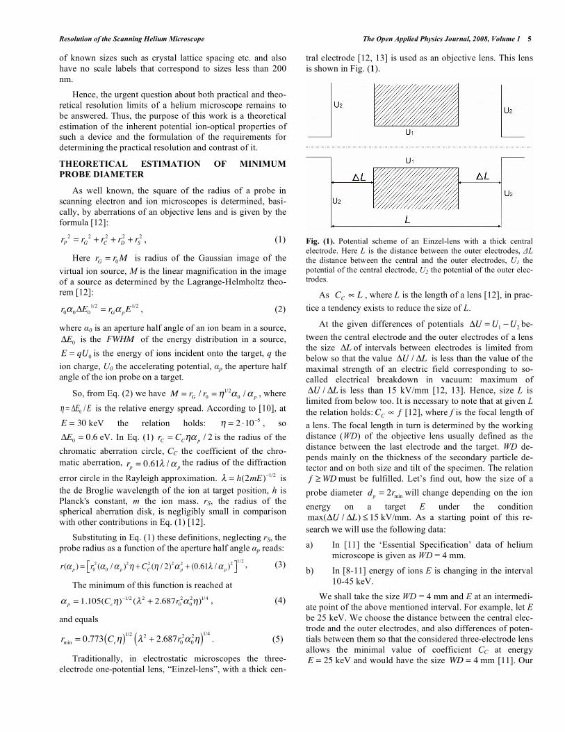
tral electrode [12, 13] is used as an objective lens. This lens is shown in Fig. (1).
Fig. (1). Potential scheme of an Einzel-lens with a thick central electrode. Here L is the distance between the outer electrodes, L the distance between the central and the outer electrodes, U1 the potential of the central electrode, U2 the potential of the outer elec-trodes.
As CC L , where L is the length of a lens [12], in prac-
tice a tendency exists to reduce the size of L.
At the given differences of potentials U =U1 U2 be-
tween the central electrode and the outer electrodes of a lens the size L of intervals between electrodes is limited from below so that the value U / L is less than the value of the maximal strength of an electric field corresponding to so-called electrical breakdown in vacuum: maximum of U / L is less than 15 kV/mm [12, 13]. Hence, size L is
limited from below too. It is necessary to note that at given L the relation holds:CC f [12], where f is the focal length of
a lens. The focal length in turn is determined by the working distance (WD) of the objective lens usually defined as the distance between the last electrode and the target. WD de-pends mainly on the thickness of the secondary particle de-tector and on both size and tilt of the specimen. The relation f WDmust be fulfilled. Let’s find out, how the size of a
probe diameter dp = 2rmin will change depending on the ion
energy on a target E under the condition max( U / L) 15 kV/mm. As a starting point of this re-
search we will use the following data:
a) In [11] the ‘Essential Specification’ data of helium microscope is given as WD = 4 mm.
b) In [8-11] energy of ions E is changing in the interval 10-45 keV.
We shall take the size WD = 4 mm and E at an intermedi-ate point of the above mentioned interval. For example, let E be 25 keV. We choose the distance between the central elec-trode and the outer electrodes, and also differences of poten-tials between them so that the considered three-electrode lens allows the minimal value of coefficient C at energy E = 25 keV and would have the size WD = 4 mm [11]. Our
6 The Open Applied Physics Journal, 2008, Volume 1 Kalbitzer and Zhukov
calculation gives the values: CC = 17 mm and dp = 0.32 nm
at E0 = 0.6 eV.
Let's change now energy of ions in an interval 5-100 kV and also proportional to all geometrical sizes of a lens so that the condition is fulfilled: max( U / L) 15 kV/mm.
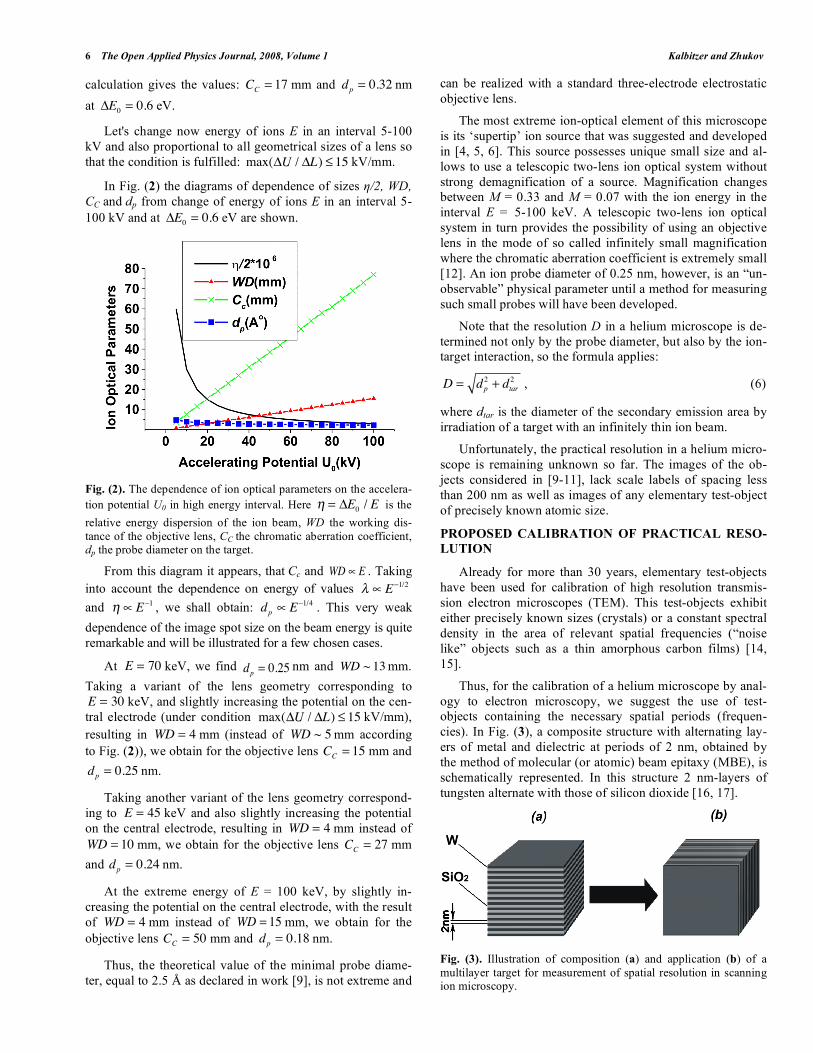
In Fig. (2) the diagrams of dependence of sizes /2, WD, CC and dp from change of energy of ions in an interval 5-100 kV and at E0 = 0.6 eV are shown.
Fig. (2). The dependence of ion optical parameters on the accelera-
tion potential U0 in high energy interval. Here = E0 / E is the
relative energy dispersion of the ion beam, WD the working dis-tance of the objective lens, CC the chromatic aberration coefficient, dp the probe diameter on the target.
From this diagram it appears, that and WD E . Taking
into account the dependence on energy of values E 1/2
and E 1 , we shall obtain: dp E 1/4 . This very weak
dependence of the image spot size on the beam energy is quite remarkable and will be illustrated for a few chosen cases.
At E = 70 keV, we find dp = 0.25 nm and WD ~ 13mm.
Taking a variant of the lens geometry corresponding to E = 30 keV, and slightly increasing the potential on the cen-tral electrode (under condition max( U / L) 15 kV/mm),
resulting in WD = 4 mm (instead of WD ~ 5mm according to Fig. (2)), we obtain for the objective lens CC = 15 mm and
dp = 0.25 nm.
Taking another variant of the lens geometry correspond-ing to E = 45 keV and also slightly increasing the potential on the central electrode, resulting in WD = 4 mm instead of WD = 10 mm, we obtain for the objective lens CC = 27 mm
and dp = 0.24 nm.
At the extreme energy of = 100 keV, by slightly in-creasing the potential on the central electrode, with the result of WD = 4 mm instead of WD = 15 mm, we obtain for the objective lens CC = 50 mm and dp = 0.18 nm.
Thus, the theoretical value of the minimal probe diame-ter, equal to 2.5 Å as declared in work [9], is not extreme and
can be realized with a standard three-electrode electrostatic objective lens.
The most extreme ion-optical element of this microscope is its ‘supertip’ ion source that was suggested and developed in [4, 5, 6]. This source possesses unique small size and al-lows to use a telescopic two-lens ion optical system without strong demagnification of a source. Magnification changes between M = 0.33 and M = 0.07 with the ion energy in the interval E = 5-100 keV. A telescopic two-lens ion optical system in turn provides the possibility of using an objective lens in the mode of so called infinitely small magnification where the chromatic aberration coefficient is extremely small [12]. An ion probe diameter of 0.25 nm, however, is an “un-observable” physical parameter until a method for measuring such small probes will have been developed.
Note that the resolution D in a helium microscope is de-termined not only by the probe diameter, but also by the ion-target interaction, so the formula applies:
D = dp2+ dtar
2 , (6)
where dtar is the diameter of the secondary emission area by irradiation of a target with an infinitely thin ion beam.
Unfortunately, the practical resolution in a helium micro-scope is remaining unknown so far. The images of the ob-jects considered in [9-11], lack scale labels of spacing less than 200 nm as well as images of any elementary test-object of precisely known atomic size.
PROPOSED CALIBRATION OF PRACTICAL RESO-
LUTION
Already for more than 30 years, elementary test-objects have been used for calibration of high resolution transmis-sion electron microscopes (TEM). This test-objects exhibit either precisely known sizes (crystals) or a constant spectral density in the area of relevant spatial frequencies (“noise like” objects such as a thin amorphous carbon films) [14, 15].
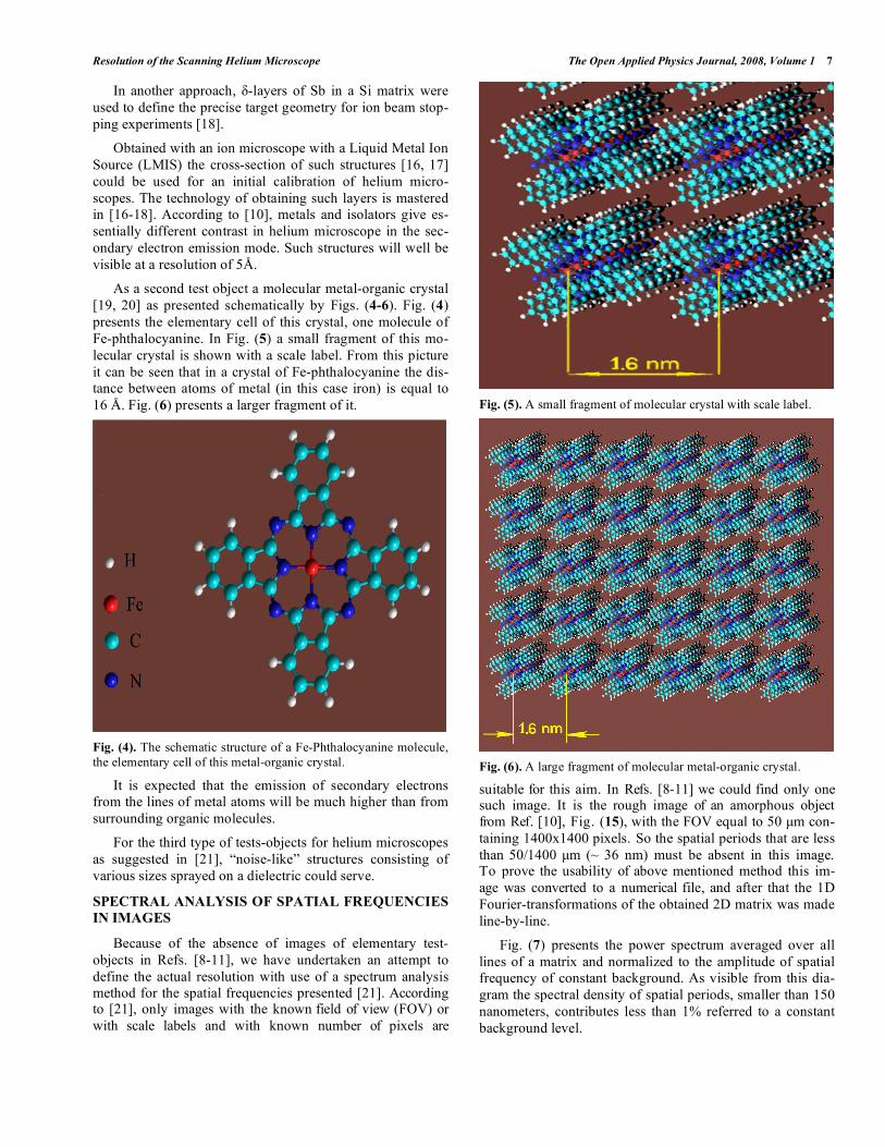
Thus, for the calibration of a helium microscope by anal-ogy to electron microscopy, we suggest the use of test-objects containing the necessary spatial periods (frequen-cies). In Fig. (3), a composite structure with alternating lay-ers of metal and dielectric at periods of 2 nm, obtained by the method of molecular (or atomic) beam epitaxy (MBE), is schematically represented. In this structure 2 nm-layers of tungsten alternate with those of silicon dioxide [16, 17].
Fig. (3). Illustration of composition (a) and application (b) of a multilayer target for measurement of spatial resolution in scanning ion microscopy.
Resolution of the Scanning Helium Microscope The Open Applied Physics Journal, 2008, Volume 1 7
In another approach, -layers of Sb in a Si matrix were used to define the precise target geometry for ion beam stop-ping experiments [18].
Obtained with an ion microscope with a Liquid Metal Ion Source (LMIS) the cross-section of such structures [16, 17] could be used for an initial calibration of helium micro-scopes. The technology of obtaining such layers is mastered in [16-18]. According to [10], metals and isolators give es-sentially different contrast in helium microscope in the sec-ondary electron emission mode. Such structures will well be visible at a resolution of 5Å.
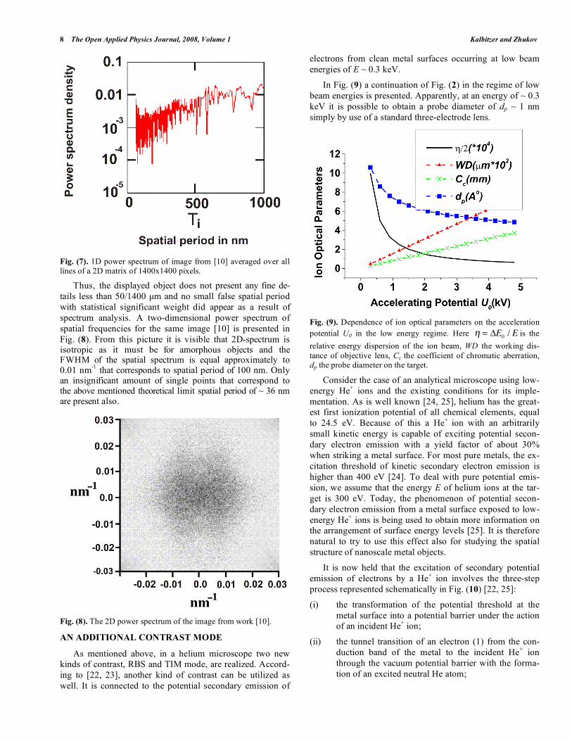
As a second test object a molecular metal-organic crystal [19, 20] as presented schematically by Figs. (4-6). Fig. (4) presents the elementary cell of this crystal, one molecule of Fe-phthalocyanine. In Fig. (5) a small fragment of this mo-lecular crystal is shown with a scale label. From this picture it can be seen that in a crystal of Fe-phthalocyanine the dis-tance between atoms of metal (in this case iron) is equal to 16 Å. Fig. (6) presents a larger fragment of it.
Fig. (4). The schematic structure of a Fe-Phthalocyanine molecule, the elementary cell of this metal-organic crystal.
It is expected that the emission of secondary electrons from the lines of metal atoms will be much higher than from surrounding organic molecules.
For the third type of tests-objects for helium microscopes as suggested in [21], “noise-like” structures consisting of various sizes sprayed on a dielectric could serve.
SPECTRAL ANALYSIS OF SPATIAL FREQUENCIES
IN IMAGES
Because of the absence of images of elementary test-objects in Refs. [8-11], we have undertaken an attempt to define the actual resolution with use of a spectrum analysis method for the spatial frequencies presented [21]. According to [21], only images with the known field of view (FOV) or with scale labels and with known number of pixels are
Fig. (5). A small fragment of molecular crystal with scale label.
Fig. (6). A large fragment of molecular metal-organic crystal.
suitable for this aim. In Refs. [8-11] we could find only one such image. It is the rough image of an amorphous object from Ref. [10], Fig. (15), with the FOV equal to 50 μm con-taining 1400x1400 pixels. So the spatial periods that are less than 50/1400 μm (~ 36 nm) must be absent in this image. To prove the usability of above mentioned method this im-age was converted to a numerical file, and after that the 1D Fourier-transformations of the obtained 2D matrix was made line-by-line.
Fig. (7) presents the power spectrum averaged over all lines of a matrix and normalized to the amplitude of spatial frequency of constant background. As visible from this dia-gram the spectral density of spatial periods, smaller than 150 nanometers, contributes less than 1% referred to a constant background level.
8 The Open Applied Physics Journal, 2008, Volume 1 Kalbitzer and Zhukov
Fig. (7). 1D power spectrum of image from [10] averaged over all lines of a 2D matrix of 1400x1400 pixels.
Thus, the displayed object does not present any fine de-tails less than 50/1400 μm and no small false spatial period with statistical significant weight did appear as a result of spectrum analysis. A two-dimensional power spectrum of spatial frequencies for the same image [10] is presented in Fig. (8). From this picture it is visible that 2D-spectrum is isotropic as it must be for amorphous objects and the FWHM of the spatial spectrum is equal approximately to 0.01 nm-1 that corresponds to spatial period of 100 nm. Only an insignificant amount of single points that correspond to the above mentioned theoretical limit spatial period of ~ 36 nm are present also.
Fig. (8). The 2D power spectrum of the image from work [10].
AN ADDITIONAL CONTRAST MODE
As mentioned above, in a helium microscope two new kinds of contrast, RBS and TIM mode, are realized. Accord-ing to [22, 23], another kind of contrast can be utilized as well. It is connected to the potential secondary emission of
electrons from clean metal surfaces occurring at low beam energies of E ~ 0.3 keV.
In Fig. (9) a continuation of Fig. (2) in the regime of low beam energies is presented. Apparently, at an energy of ~ 0.3 keV it is possible to obtain a probe diameter of dp ~ 1 nm simply by use of a standard three-electrode lens.
Fig. (9). Dependence of ion optical parameters on the acceleration
potential U0 in the low energy regime. Here = E0 / E is the
relative energy dispersion of the ion beam, WD the working dis-tance of objective lens, Cc the coefficient of chromatic aberration, dp the probe diameter on the target.
Consider the case of an analytical microscope using low-energy He+ ions and the existing conditions for its imple-mentation. As is well known [24, 25], helium has the great-est first ionization potential of all chemical elements, equal to 24.5 eV. Because of this a He+ ion with an arbitrarily small kinetic energy is capable of exciting potential secon-dary electron emission with a yield factor of about 30% when striking a metal surface. For most pure metals, the ex-citation threshold of kinetic secondary electron emission is higher than 400 eV [24]. To deal with pure potential emis-sion, we assume that the energy E of helium ions at the tar-get is 300 eV. Today, the phenomenon of potential secon-dary electron emission from a metal surface exposed to low-energy He+ ions is being used to obtain more information on the arrangement of surface energy levels [25]. It is therefore natural to try to use this effect also for studying the spatial structure of nanoscale metal objects.
It is now held that the excitation of secondary potential emission of electrons by a He+ ion involves the three-step process represented schematically in Fig. (10) [22, 25]:
(i) the transformation of the potential threshold at the metal surface into a potential barrier under the action of an incident He+ ion;
(ii) the tunnel transition of an electron (1) from the con-duction band of the metal to the incident He+ ion through the vacuum potential barrier with the forma-tion of an excited neutral He atom;
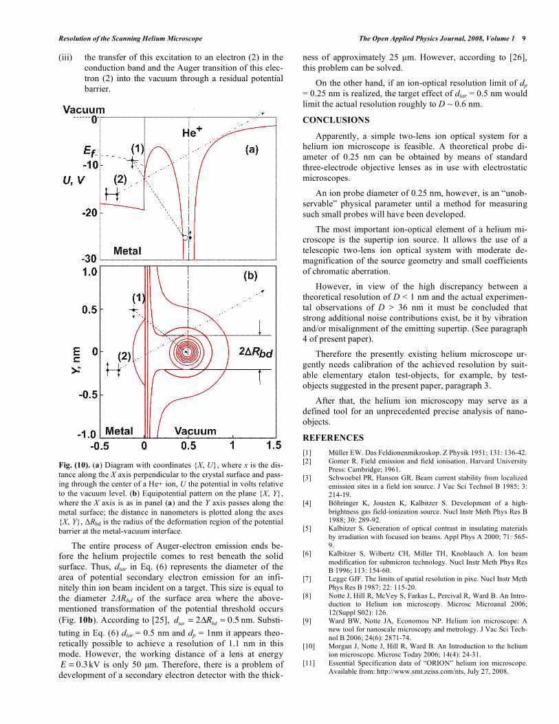
Resolution of the Scanning Helium Microscope The Open Applied Physics Journal, 2008, Volume 1 9
(iii) the transfer of this excitation to an electron (2) in the conduction band and the Auger transition of this elec-tron (2) into the vacuum through a residual potential barrier.
Fig. (10). (a) Diagram with coordinates {X, U}, where x is the dis-tance along the X axis perpendicular to the crystal surface and pass-ing through the center of a He+ ion, U the potential in volts relative to the vacuum level. (b) Equipotential pattern on the plane {X, Y}, where the X axis is as in panel (a) and the Y axis passes along the metal surface; the distance in nanometers is plotted along the axes {X, Y}, Rbd is the radius of the deformation region of the potential barrier at the metal-vacuum interface.
The entire process of Auger-electron emission ends be-fore the helium projectile comes to rest beneath the solid surface. Thus, dtar in Eq. (6) represents the diameter of the area of potential secondary electron emission for an infi-nitely thin ion beam incident on a target. This size is equal to the diameter 2 Rbd of the surface area where the above-mentioned transformation of the potential threshold occurs (Fig. 10b). According to [25], dtar = 2 Rbd 0.5 nm. Substi-
tuting in Eq. (6) dtar = 0.5 nm and dp = 1nm it appears theo-retically possible to achieve a resolution of 1.1 nm in this mode. However, the working distance of a lens at energy E = 0.3kV is only 50 μm. Therefore, there is a problem of development of a secondary electron detector with the thick-
ness of approximately 25 μm. However, according to [26], this problem can be solved.
On the other hand, if an ion-optical resolution limit of dp = 0.25 nm is realized, the target effect of dtar = 0.5 nm would limit the actual resolution roughly to D ~ 0.6 nm.
CONCLUSIONS
Apparently, a simple two-lens ion optical system for a helium ion microscope is feasible. A theoretical probe di-ameter of 0.25 nm can be obtained by means of standard three-electrode objective lenses as in use with electrostatic microscopes.
An ion probe diameter of 0.25 nm, however, is an “unob-servable” physical parameter until a method for measuring such small probes will have been developed.
The most important ion-optical element of a helium mi-croscope is the supertip ion source. It allows the use of a telescopic two-lens ion optical system with moderate de-magnification of the source geometry and small coefficients of chromatic aberration.
However, in view of the high discrepancy between a theoretical resolution of D < 1 nm and the actual experimen-tal observations of D > 36 nm it must be concluded that strong additional noise contributions exist, be it by vibration and/or misalignment of the emitting supertip. (See paragraph 4 of present paper).
Therefore the presently existing helium microscope ur-gently needs calibration of the achieved resolution by suit-able elementary etalon test-objects, for example, by test-objects suggested in the present paper, paragraph 3.
After that, the helium ion microscopy may serve as a defined tool for an unprecedented precise analysis of nano-objects.
REFERENCES
[1] Müller EW. Das Feldionenmikroskop. Z Physik 1951; 131: 136-42. [2] Gomer R. Field emission and field ionisation. Harvard University
Press: Cambridge; 1961. [3] Schwoebel PR, Hanson GR. Beam current stability from localized
emission sites in a field ion source. J Vac Sci Technol B 1985; 3: 214-19.
[4] Böhringer K, Jousten K, Kalbitzer S. Development of a high-brightness gas field-ionization source. Nucl Instr Meth Phys Res B 1988; 30: 289-92.
[5] Kalbitzer S. Generation of optical contrast in insulating materials by irradiation with focused ion beams. Appl Phys A 2000; 71: 565-9.
[6] Kalbitzer S, Wilbertz CH, Miller TH, Knoblauch A. Ion beam modification for submicron technology. Nucl Instr Meth Phys Res B 1996; 113: 154-60.
[7] Legge GJF. The limits of spatial resolution in pixe. Nucl Instr Meth Phys Res B 1987; 22: 115-20.
[8] Notte J, Hill R, McVey S, Farkas L, Percival R, Ward B. An Intro-duction to Helium ion microscopy. Microsc Microanal 2006; 12(Suppl S02): 126.
[9] Ward BW, Notte JA, Economou NP. Helium ion microscope: A new tool for nanoscale microscopy and metrology. J Vac Sci Tech-nol B 2006; 24(6): 2871-74.
[10] Morgan J, Notte J, Hill R, Ward B. An Introduction to the helium ion microscope. Microsc Today 2006; 14(4): 24-31.
[11] Essential Specification data of “ORION” helium ion microscope. Available from: http://www.smt.zeiss.com/nts, July 27, 2008.
10 The Open Applied Physics Journal, 2008, Volume 1 Kalbitzer and Zhukov
[12] Szilagyi M. Electron and ion optics. Plenum Press: New York; 1988.
[13] Grivet P. Electron optics. Pergamon Press: New York; 1965. [14] Heidenreich R. Fundamentals of Transmission Electron Micros-
copy. Interscience Publisher: New York, London, Sydney; 1964. [15] Spense J. Experimental high resolution electron microscopy. Clar-
endon Press: Oxford; 1981. [16] Driskill-Smith AAG, Hasko DG, Ahmed H. The “nanotriode:” A
nanoscale field-emission tube. Appl Phys Let 1999; 75(18): 2845-47.
[17] Driskill-Smith AAG, Hasko DG, Ahmed H. Quantum interference in vacuum nanotriode. J Vac Sci Technol B 2000; 18(6): 3481-87.
[18] Niemann D, Oberschachtsiek P, Kalbitzer S. Energy loss and strggling of MeV 4He ions in a Si/Sb multilayer target. Nucl Instr Meth Phys Res B 1993; 80-81: 37-40.
[19] Engel MK, Kawamura RKH. Single-Crystal and Solid-State Mo-lecular Structures of Phthalocyanine Complexes. 1996. Available from: http://phthalo.mkengel.de/KICReview.pdf, July 27, 2008.
[20] Li-Ying C, Yang J, Fu Q, Bao-Zhong Z, Tian L, Hai-Ling Y. Syn-thesis, crystal structure and characterization of a new zinc phthalo-cyanine complex. J Mol Struct 2007; 827(1): 149-54.
[21] Orloff J, Swanson LW, Utlaut M. Fundamental limits to imaging resolution for focused ion beams. J Vac Sci Technol B 1996; 14(6): 3759-63.
[22] Zhukov VA, Titov AI, Zavyalova AV. Using a chromatic-aberration correction system to achieve sub-1.6-nm resolutions of a focused-ion-beam microscope designed for characterization and processing. Russian Microelectronics 2007; 36 (6): 279-87.
[23] Zhukov VA. Achieving sub-1.6-nm resolutions of a low-voltage microscopic focused-ion-beam system not involving aberration cor-rection. Russ Microelec 2008; 37(2): 98-106.
[24] Petrov NN, Abroyan I. Diagnostika poverkhnosti s pomoshchyu ionnykh puchkov (ion-beam characterization of surfaces). Nauka: Leningrad; 1977.
[25] Cazalilla MA, Lorente N, Diez MR. Theory of auger neutralization and deexcitation of slow ions at metal surfaces. Phys Rev B 1998; 58(20): 13991-4006.
[26] Schenkel T, Persaud A, Park SJ, et al. Single ion implantation for solid state quantum computer development. J Vac Sci Technol B 2002; 20(6): 2819-23.
Received: May 16, 2008 Revised: July 10, 2008 Accepted: July 14, 2008
© Kalbitzer and Zhukov; Licensee Bentham Open.
This is an open access article licensed under the terms of the Creative Commons Attribution Non-Commercial License (http://creativecommons.org/licenses/by-nc/3.0/) which permits unrestricted, non-commercial use, distribution and reproduction in any medium, provided the work is properly cited.