refinement of unified random access memorynobent.kaist.ac.kr/paper/2009/fj_seong-wan...
TRANSCRIPT
IEEE TRANSACTIONS ON ELECTRON DEVICES, VOL. 56, NO. 4, APRIL 2009 601
Refinement of Unified Random Access MemorySeong-Wan Ryu, Jin-Woo Han, Chung-Jin Kim, Sung-Jin Choi, Sungho Kim, Jin-Soo Kim, Kwang Hee Kim,
Jae-Sub Oh, Meyong-Ho Song, Gi-Sung Lee, Yun Chang Park, Jeoung Woo Kim, and Yang-Kyu Choi
Abstract—This paper investigates how gate height (Hg), whichrefers to the size of a floating-body, affects the program efficiencyand retention characteristics of one-transistor DRAM (1T-DRAM)and nonvolatile memory (NVM) for a FinFET SONOS device thathas a partially depleted silicon-on-insulator (PDSOI) region as acharge storage node for a 1T-DRAM operation. A device with alower Hg yields enhanced program efficiency due to the higherimpact ionization rate caused by the enlarged PDSOI region forboth 1T-DRAM and NVM operations. The device with the lowerHg shows slightly poor retention characteristics in the NVMunlike the 1T-DRAM.
Index Terms—FinFET, gate height, nonvolatile memory, one-transistor DRAM (1T-DRAM), partially depleted silicon-on-insulator (PDSOI), SONOS, unified random access memory(URAM).
I. INTRODUCTION
THE development of silicon technology must deal withtwo major issues in the digital convergence era. One
issue is concerned with scalability for high density and per-formance. With regard to downscaling, a FinFET structure ishighly preferable due to its enhanced immunity to short-channeleffects (SCEs) through high gate controllability [1]–[3]. Theother issue comes with the integration of multifunctional de-vices for the demands of system-on-chip (SoC) technology. Aprevious multifunctional device that fused nonvolatile mem-ory (NVM) [4]–[10] and a one-transistor DRAM (1T-DRAM)[11]–[17] in a single cell was reported, even though individ-ual data access could not be allowed because of the wafer-level back gate for NVM operation [18]. Thus, a new typeof multifunctional unified random access memory (URAM)based on a FinFET structure was proposed by considering theaforementioned two issues [19].
The URAM has two distinctive storage nodes: oxide/nitride/oxide (O/N/O) stacks for NVM operation and a partiallydepleted silicon-on-insulator (PDSOI) region for 1T-DRAMoperation. When the URAM is applied as a substitute forNVM and DRAM parts of SoC, the URAM can provide highefficiency by dynamic allocation of storage capacity accordingto customization of functionality for each part of NVM and
Manuscript received May 6, 2008; revised December 1, 2008. First publishedFebruary 3, 2009; current version published March 25, 2009. This work wassupported by the National Research Program for the 0.1-Terabit NonvolatileMemory Development Initiative, which is sponsored by the Korean Ministryof Commerce, Industry and Energy. The review of this paper was arranged byEditor C.-Y. Lu.
S.-W. Ryu, J.-W. Han, C.-J. Kim, S.-J. Choi, S. Kim, and Y.-K. Choi arewith the Division of Electrical Engineering, School of Electrical Engineeringand Computer Science, Korea Advanced Institute of Science and Technology,Daejeon 305-701, Korea (e-mail: [email protected]).
J.-S. Kim, K. H. Kim, J.-S. Oh, M.-H. Song, G.-S. Lee, Y. C. Park, andJ. W. Kim are with the National NanoFab Center, Daejeon 305-806, Korea.
Digital Object Identifier 10.1109/TED.2008.2012292
DRAM without introducing an additional chip. Also, withrespect to multichip-package (MCP) application as well asSoC application, the URAM (transistor-level fusion) can havemore strength in highly efficient data storage than MCP, whichincludes both a customized intrinsic NVM part and a DRAMpart due to the aforementioned reason as another application.
In the proposed URAM structure, the PDSOI and FDSOIregions simultaneously exist in a single cell, and its ratio istunable. The PDSOI region in a FinFET SONOS structure ofthe URAM is determined by Hg , which incompletely coversthe entire fin height (Hfin), as shown in Fig. 1. The uncoveredportion of the fin remains as a part of the PDSOI region. ThePDSOI region can be enlarged by simply reducing Hg . It isconsiderable how this unique feature of the URAM has strengthfor the 1T-DRAM operation as well as a flash memory opera-tion. Related to the 1T-DRAM operation of the URAM, therealready exist 3-D FinFET-structural 1T-DRAMs [15], [16] aswell as planar types [11]–[14]. When the fin is narrow enoughto be fully depleted for the high SCE immunity, the FDSOIfin region is insufficient to store holes for an enough sensingmargin. Thus, a back-gate bias should be applied to hold holes,but it increases operation complexity. However, in the URAMstructure, the FDSOI of the channel region suppresses theSCEs, and the PDSOI region can accommodate an increasedamount of charges and improve the retention characteristics of1T-DRAM. Also, Hg modulation can affect the SCEs which aredirectly related to a hot-carrier injection. This can react to theprogram efficiency of the NVM in a different way.
In the design of a FinFET structure, the fin width (Wfin)is a crucial parameter for enhancing the NVM performanceand reliability [7]–[10] and for suppressing the SCEs [1]–[3].However, the gate height (Hg) has seldom been considered asa meaningful optimization parameter. By modulating the Hg ofthe URAM, a well-designed PDSOI region can accommodatean increased amount of charges and improve the retentioncharacteristics of 1T-DRAM as mentioned before. Also, Hg
modulation can affect the SCEs which are directly related toa hot-carrier injection. This can react to the program efficiencyof the NVM in a different way. Under these considerations, theHg effects on program efficiency and retention characteristicsare investigated to optimize both the NVM and 1T-DRAMcharacteristics of the URAM.
II. FABRICATION
Based on a p-type (100) SOI wafer, a silicon body wasdefined and narrowed down to 30 nm by means of a trimmingprocess after Si3N4 deposition of a hard-mask layer on a110-nm-thick SOI wafer and a 370-nm-thick buried oxide.
0018-9383/$25.00 © 2009 IEEE
Authorized licensed use limited to: Korea Advanced Institute of Science and Technology. Downloaded on March 24, 2009 at 14:47 from IEEE Xplore. Restrictions apply.

602 IEEE TRANSACTIONS ON ELECTRON DEVICES, VOL. 56, NO. 4, APRIL 2009
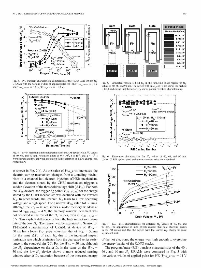
Fig. 1. (a) Schematic, (b) bird’s-eye view (SEM image), (c) different Hg values (of 40, 66, and 90 nm) (TEM images), and (d) cross-sectional TEM image,where the thicknesses of the O/N/O layers (3 nm/6 nm/4 nm) are confirmed.
High-density plasma SiO2 was deposited as a sacrificial layerto control Hg . After chemical–mechanical polishing, the valueof Hg was determined by an additional high-density plasmaSiO2 etching. Stacks of O/N/O (3 nm/6 nm/4 nm) were grownand deposited. Finally, gate patterning was performed aftera 30-nm in situ N+ polycrystalline silicon deposition, andarsenic ions were implanted to form source–drain junctions.Fig. 1 shows a URAM schematic of a PDSOI FinFET SONOSstructure and cross-sectional transmission electron microscopy(TEM) images for different gate heights of 40, 66, and 90 nm.The thicknesses of the O/N/O layers (3 nm/6 nm/4 nm) wereconfirmed from the TEM image of Fig. 1(d). The measureddevices have a nominal gate length of 190 nm and a fin width(Wfin) of 50 nm.
III. DEVICE CHARACTERISTICS AND DISCUSSION
The URAM concept utilizes two distinct operations of NVMand 1T-DRAM in a single cell. Each operation requires theassignment of a separate charge storage node, namely, a floatinggate of O/N/O stacks for NVM operation and a floating-body ofPDSOI for 1T-DRAM operation. A 1T-DRAM operating modeis available only for state “0” of NVM. In the programmed state(state “1”) of NVM, the interference by elevated 1T-DRAMprogram conditions is inevitably induced to store charges in thefloating gate, and a proper 1T-DRAM sensing margin can sub-sequently be decreased. Thus, during the program and retentionmodes of the NVM operation, the 1T-DRAM operation modeis at a standby state. The effects of the 1T-DRAM and NVM onHg modulation are discussed later.
A. NVM Characteristics of URAM
Fig. 2(a) shows the IDS−VGS transfer characteristics ofthe Hg = 40-, 66-, and 90-nm URAMs (Wfin = 50 nm) fordifferent program conditions (VDS_PGM = 3 and 4.5 V) withfixed VGS_PGM = 11 V and τPGM = 80 μs. Based on these
Fig. 2. (a) For Hg = 40-, 66-, and 90-nm URAMs (Wfin = 50 nm)and IDS−VGS transfer characteristics with different program conditions ofVDS_PGM = 3 V and VDS_PGM = 4.5 V. (b) Program window characteris-tics as a function of VDS_PGM for different Wfin values (of 30 and 50 nm) andthree different Hg values (of 40, 66, and 90 nm) for each Wfin. The best overallprogram efficiency was attained with the lowest Hg of 40 nm. This trend wasamplified by a narrowed Wfin.
transfer curves, the NVM program characteristics are measuredas a function of drain voltage (VDS_PGM) with a constant gatevoltage (VGS_PGM = 11 V) for different Wfin values (of 30and 50 nm) and different Hg values (of 40, 66, and 90 nm),
Authorized licensed use limited to: Korea Advanced Institute of Science and Technology. Downloaded on March 24, 2009 at 14:47 from IEEE Xplore. Restrictions apply.
RYU et al.: REFINEMENT OF UNIFIED RANDOM ACCESS MEMORY 603
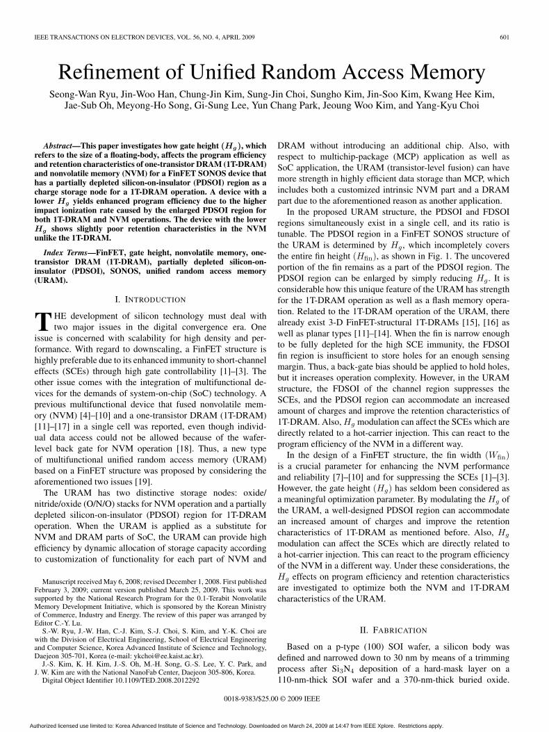
Fig. 3. P/E transient characteristic comparison of the 40, 66-, and 90-nm Hg
URAMs with the various widths of applied pulse for P/E (VGS_PGM = 11 Vand VDS_PGM = 4.5 V/VGS_ERS = −13 V).
Fig. 4. NVM retention time characteristics for URAM devices with Hg valuesof 40, 66, and 90 nm. Retention times of 9 × 10⁵, 5 × 10⁶, and 2 × 10⁷ swere extrapolated by applying a retention failure criterion of a 20% charge loss,respectively.
as shown in Fig. 2(b). As the value of VDS_PGM increases, theelectron-storing mechanism changes from a tunneling mecha-nism to a channel hot-electron injection (CHEI) mechanism,and the electron stored by the CHEI mechanism triggers asudden elevation of the threshold voltage shift (ΔVth). For boththe Wfin devices, the triggering point (VDS_PGM) for the chargestored by the CHEI mechanism was declined with the loweredHg . In other words, the lowered Hg leads to a low operatingvoltage and a high speed. For a narrow Wfin value (of 30 nm),although the Hg = 40 nm shows a wider memory window ataround VDS_PGM = 4 V, the memory window increment wasnot observed in the rest of the Hg values, even at VDS_PGM =6 V. This explicit difference is from the high impact ionizationrate of the low Hg . The reason will be explained in Session B:1T-DRAM characteristics of URAM. A device of Wfin =50 nm has a lower VDS_PGM value than that of Wfin = 30 nmfor the same ΔVth of each Hg due to the increased impactionization rate which originates from the decreased series resis-tance in the source/drain [20]. For the Wfin = 50 nm, althoughthe Hg dependence on the ΔVth is the same as the Wfin =30 nm, the low-Hg device shows a more reduced sensingwindow after ΔVth saturation because of the increased energy
Fig. 5. Simulated vertical E-field Ey in the tunneling oxide region for Hg
values of 40, 66, and 90 nm. The device with an Hg of 40 nm shows the highestE-field, indicating that the lower Hg shows poorer retention characteristics.
Fig. 6. Endurance characteristics for Hg values of 40, 66, and 90 nm.Up to 105 P/E cycles, good endurance characteristics were obtained.
Fig. 7. IDS−VGS characteristics for different Hg values of 40, 66, and90 nm. The appearance of kink effects ensures that hole charging occursin the PD region and that the device with the lowest Hg shows the mostsignificant kink.
of the hot electrons; the energy was high enough to overcomethe energy barrier of the O/N/O stacks.
The program/erase (P/E) transient characteristics of the 40-,66-, and 90-nm Hg URAMs were compared in Fig. 3 withthe various widths of applied pulse for P/E (VGS_PGM = 11 V
Authorized licensed use limited to: Korea Advanced Institute of Science and Technology. Downloaded on March 24, 2009 at 14:47 from IEEE Xplore. Restrictions apply.
604 IEEE TRANSACTIONS ON ELECTRON DEVICES, VOL. 56, NO. 4, APRIL 2009
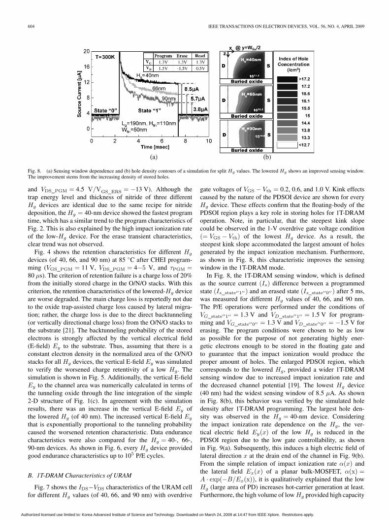
Fig. 8. (a) Sensing window dependence and (b) hole density contours of a simulation for split Hg values. The lowered Hg shows an improved sensing window.The improvement stems from the increasing density of stored holes.
and VDS_PGM = 4.5 V/VGS_ERS = −13 V). Although thetrap energy level and thickness of nitride of three differentHg devices are identical due to the same recipe for nitridedeposition, the Hg = 40-nm device showed the fastest programtime, which has a similar trend to the program characteristics ofFig. 2. This is also explained by the high impact ionization rateof the low-Hg device. For the erase transient characteristics,clear trend was not observed.
Fig. 4 shows the retention characteristics for different Hg
devices (of 40, 66, and 90 nm) at 85 ◦C after CHEI program-ming (VGS_PGM = 11 V, VDS_PGM = 4−5 V, and τPGM =80 μs). The criterion of retention failure is a charge loss of 20%from the initially stored charge in the O/N/O stacks. With thiscriterion, the retention characteristics of the lowered-Hg deviceare worse degraded. The main charge loss is reportedly not dueto the oxide trap-assisted charge loss caused by lateral migra-tion; rather, the charge loss is due to the direct backtunneling(or vertically directional charge loss) from the O/N/O stacks tothe substrate [21]. The backtunneling probability of the storedelectrons is strongly affected by the vertical electrical field(E-field) Ey to the substrate. Thus, assuming that there is aconstant electron density in the normalized area of the O/N/Ostacks for all Hg devices, the vertical E-field Ey was simulatedto verify the worsened charge retentivity of a low Hg . Thesimulation is shown in Fig. 5. Additionally, the vertical E-fieldEy to the channel area was numerically calculated in terms ofthe tunneling oxide through the line integration of the simple2-D structure of Fig. 1(c). In agreement with the simulationresults, there was an increase in the vertical E-field Ey ofthe lowered Hg (of 40 nm). The increased vertical E-field Ey
that is exponentially proportional to the tunneling probabilitycaused the worsened retention characteristic. Data endurancecharacteristics were also compared for the Hg = 40-, 66-,90-nm devices. As shown in Fig. 6, every Hg device providedgood endurance characteristics up to 105 P/E cycles.
B. 1T-DRAM Characteristics of URAM
Fig. 7 shows the IDS−VDS characteristics of the URAM cellfor different Hg values (of 40, 66, and 90 nm) with overdrive
gate voltages of VGS − Vth = 0.2, 0.6, and 1.0 V. Kink effectscaused by the nature of the PDSOI device are shown for everyHg device. These effects confirm that the floating-body of thePDSOI region plays a key role in storing holes for 1T-DRAMoperation. Note, in particular, that the steepest kink slopecould be observed in the 1-V overdrive gate voltage condition(= VGS − Vth) of the lowest Hg device. As a result, thesteepest kink slope accommodated the largest amount of holesgenerated by the impact ionization mechanism. Furthermore,as shown in Fig. 8, this characteristic improves the sensingwindow in the 1T-DRAM mode.
In Fig. 8, the 1T-DRAM sensing window, which is definedas the source current (Is) difference between a programmedstate (Is_state′′1′′) and an erased state (Is_state′′0′′) after 5 ms,was measured for different Hg values of 40, 66, and 90 nm.The P/E operations were performed under the conditions ofVG_state′′1′′ = 1.3 V and VD_state′′1′′ = 1.5 V for program-ming and VG_state′′0′′ = 1.3 V and VD_state′′0′′ = −1.5 V forerasing. The program conditions were chosen to be as lowas possible for the purpose of not generating highly ener-getic electrons enough to be stored in the floating gate andto guarantee that the impact ionization would produce theproper amount of holes. The enlarged PDSOI region, whichcorresponds to the lowered Hg , provided a wider 1T-DRAMsensing window due to increased impact ionization rate andthe decreased channel potential [19]. The lowest Hg device(40 nm) had the widest sensing window of 8.5 μA. As shownin Fig. 8(b), this behavior was verified by the simulated holedensity after 1T-DRAM programming. The largest hole den-sity was observed in the Hg = 40-nm device. Consideringthe impact ionization rate dependence on the Hg , the ver-tical electric field Ey(x) of the low Hg is reduced in thePDSOI region due to the low gate controllability, as shownin Fig. 9(a). Subsequently, this induces a high electric field oflateral direction x at the drain end of the channel in Fig. 9(b).From the simple relation of impact ionization rate α(x) andthe lateral field Ex(x) of a planar bulk-MOSFET, α(x) =A · exp(−B/Ex(x)), it is qualitatively explained that the lowHg (large area of PD) increases hot-carrier generation at least.Furthermore, the high volume of low Hg provided high capacity
Authorized licensed use limited to: Korea Advanced Institute of Science and Technology. Downloaded on March 24, 2009 at 14:47 from IEEE Xplore. Restrictions apply.

RYU et al.: REFINEMENT OF UNIFIED RANDOM ACCESS MEMORY 605
Fig. 9. (a) Simulated vertical E-field Ey and (b) lateral E-field Ex inthe PDSOI region after 1T-DRAM program operation (VGS = 1.3 V andVDS = 1.5 V).
for storing the generated holes which enhances the programefficiency.
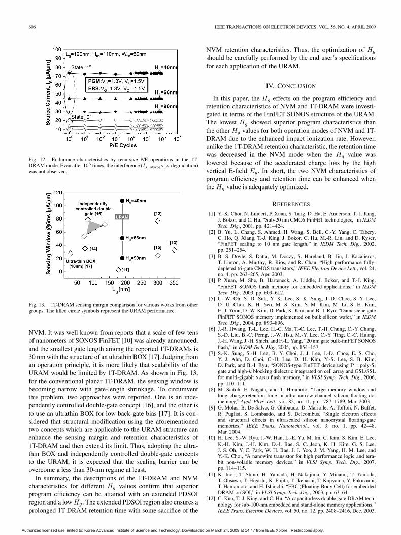
P/E transient characteristics are shown in Fig. 10 for the 1T-DRAM operation of the URAM device in Fig. 7. For eachheight of the URAM cell, the sensing current (Is) by the P/Eoperations was saturated at 10 ns, ensuring a high P/E speed.Note that devices with Hg of 40 and 66 nm satisfy the sensingwindow by more than 5 μA (i.e., Is_state′′1′′ − Is_state′′0′′ )with a P/E time that is even shorter than 10 ns. This speed iscomparable to that of a conventional DRAM level.
As shown in Fig. 11(a), the 1T-DRAM retention time neededto satisfy the sensing window (> 5 μA) was measured. Anexcellent retention time of 260 ms was achieved for the1T-DRAM operation with an Hg value of 40 nm. From thesimulated potential curves in Fig. 11(b) for different Hg values(of 40, 66, and 90 nm), the device with Hg of 40 nm has thelowest potential for holding holes in the PDSOI region. Thispotential is a crucial factor for proving the longest retentiontime for hole storability.
A major concern in the URAM is the interference betweenthe two distinctive charge storage nodes of floating gate andfloating-body. Fig. 12 shows Is after iterative P/E in the 1T-DRAM operation mode. For the 1T-DRAM programming op-eration, the harsh bias conditions appear to evoke an Is_state′′1′′
decrement caused by soft programming. In this type of pro-
Fig. 10. P/E transient characteristics of the URAM in the 1T-DRAM mode.A sufficient sensing window was observed at 10 ns of P/E time for devices withHg values of 40 and 66 nm.
Fig. 11. (a) 1T-DRAM retention characteristics and (b) simulated potentialcurves in the floating-body region. The lowered Hg guarantees an increase inhole storability due to the lowered potential.
gramming, electrons are stored by the CHEI mechanism inthe floating gate of the NVM as a charge storage node. Thisphenomenon may destructively narrow the sensing windowas a result of the nonvolatility of the data from soft pro-gramming. However, the decrement of Is_state′′1′′ was notobserved, even after 106 repetitive P/E cycles in the 1T-DRAMoperation mode.
The 1T-DRAM has more difficulty in scalability due to thelimited body volume (capacitance) compared to the SONOS
Authorized licensed use limited to: Korea Advanced Institute of Science and Technology. Downloaded on March 24, 2009 at 14:47 from IEEE Xplore. Restrictions apply.
606 IEEE TRANSACTIONS ON ELECTRON DEVICES, VOL. 56, NO. 4, APRIL 2009
Fig. 12. Endurance characteristics by recursive P/E operations in the 1T-DRAM mode. Even after 106 times, the interference (Is_state′′1′′ degradation)was not observed.
Fig. 13. 1T-DRAM sensing margin comparison for various works from othergroups. The filled circle symbols represent the URAM performance.
NVM. It was well known from reports that a scale of few tensof nanometers of SONOS FinFET [10] was already announced,and the smallest gate length among the reported 1T-DRAMs is30 nm with the structure of an ultrathin BOX [17]. Judging froman operation principle, it is more likely that scalability of theURAM would be limited by 1T-DRAM. As shown in Fig. 13,for the conventional planar 1T-DRAM, the sensing window isbecoming narrow with gate-length shrinkage. To circumventthis problem, two approaches were reported. One is an inde-pendently controlled double-gate concept [16], and the other isto use an ultrathin BOX for low back-gate bias [17]. It is con-sidered that structural modification using the aforementionedtwo concepts which are applicable to the URAM structure canenhance the sensing margin and retention characteristics of1T-DRAM and then extend its limit. Thus, adopting the ultra-thin BOX and independently controlled double-gate conceptsto the URAM, it is expected that the scaling barrier can beovercome a less than 30-nm regime at least.
In summary, the descriptions of the 1T-DRAM and NVMcharacteristics for different Hg values confirm that superiorprogram efficiency can be attained with an extended PDSOIregion and a low Hg . The extended PDSOI region also ensures aprolonged 1T-DRAM retention time with some sacrifice of the
NVM retention characteristics. Thus, the optimization of Hg
should be carefully performed by the end user’s specificationsfor each application of the URAM.
IV. CONCLUSION
In this paper, the Hg effects on the program efficiency andretention characteristics of NVM and 1T-DRAM were investi-gated in terms of the FinFET SONOS structure of the URAM.The lowest Hg showed superior program characteristics thanthe other Hg values for both operation modes of NVM and 1T-DRAM due to the enhanced impact ionization rate. However,unlike the 1T-DRAM retention characteristic, the retention timewas decreased in the NVM mode when the Hg value waslowered because of the accelerated charge loss by the highvertical E-field Ey . In short, the two NVM characteristics ofprogram efficiency and retention time can be enhanced whenthe Hg value is adequately optimized.
REFERENCES
[1] Y.-K. Choi, N. Lindert, P. Xuan, S. Tang, D. Ha, E. Anderson, T.-J. King,J. Bokor, and C. Hu, “Sub-20 nm CMOS FinFET technologies,” in IEDMTech. Dig., 2001, pp. 421–424.
[2] B. Yu, L. Chang, S. Ahmed, H. Wang, S. Bell, C.-Y. Yang, C. Tabery,C. Ho, Q. Xiang, T.-J. King, J. Bokor, C. Hu, M.-R. Lin, and D. Kyser,“FinFET scaling to 10 nm gate length,” in IEDM Tech. Dig., 2002,pp. 251–254.
[3] B. S. Doyle, S. Datta, M. Doczy, S. Hareland, B. Jin, J. Kacalieros,T. Linton, A. Murthy, R. Rios, and R. Chau, “High performance fully-depleted tri-gate CMOS transistors,” IEEE Electron Device Lett., vol. 24,no. 4, pp. 263–265, Apr. 2003.
[4] P. Xuan, M. She, B. Harteneck, A. Liddle, J. Bokor, and T.-J. King,“FinFET SONOS flash memory for embedded applications,” in IEDMTech. Dig., 2003, pp. 609–612.
[5] C. W. Oh, S. D. Suk, Y. K. Lee, S. K. Sung, J.-D. Choe, S.-Y. Lee,D. U. Choi, K. H. Yeo, M. S. Kim, S.-M. Kim, M. Li, S. H. Kim,E.-J. Yoon, D.-W. Kim, D. Park, K. Kim, and B.-I. Ryu, “Damascene gateFinFET SONOS memory implemented on bulk silicon wafer,” in IEDMTech. Dig., 2004, pp. 893–896.
[6] J.-R. Hwang, T.-L. Lee, H.-C. Ma, T.-C. Lee, T.-H. Chung, C.-Y. Chang,S.-D. Liu, B.-C. Perng, J.-W. Hsu, M.-Y. Lee, C.-Y. Ting, C.-C. Huang,J.-H. Wang, J.-H. Shieh, and F.-L. Yang, “20 nm gate bulk-finFET SONOSflash,” in IEDM Tech. Dig., 2005, pp. 154–157.
[7] S.-K. Sung, S.-H. Lee, B. Y. Choi, J. J. Lee, J.-D. Choe, E. S. Cho,Y. J. Ahn, D. Choi, C.-H. Lee, D. H. Kim, Y.-S. Lee, S. B. Kim,D. Park, and B.-I. Ryu, “SONOS-type FinFET device using P+ poly-Sigate and high-k blocking dielectric integrated on cell array and GSL/SSLfor multi-gigabit NAND flash memory,” in VLSI Symp. Tech. Dig., 2006,pp. 110–111.
[8] M. Saitoh, E. Nagata, and T. Hiramoto, “Large memory window andlong charge-retention time in ultra narrow-channel silicon floating-dotmemory,” Appl. Phys. Lett., vol. 82, no. 11, pp. 1787–1789, Mar. 2003.
[9] G. Molas, B. De Salvo, G. Ghibaudo, D. Mariolle, A. Toffoli, N. Buffet,R. Puglisi, S. Lombardo, and S. Deleonibus, “Single electron effectsand structural effects in ultrascaled silicon nanocrystal floating-gatememories,” IEEE Trans. Nanotechnol., vol. 3, no. 1, pp. 42–48,Mar. 2004.
[10] H. Lee, S.-W. Ryu, J.-W. Han, L.-E. Yu, M. Im, C. Kim, S. Kim, E. Lee,K.-H. Kim, J.-H. Kim, D.-I. Bae, S. C. Jeon, K. H. Kim, G. S. Lee,J. S. Oh, Y. C. Park, W. H. Bae, J. J. Yoo, J. M. Yang, H. M. Lee, andY.-K. Choi, “A nanowire transistor for high performance logic and tera-bit non-volatile memory devices,” in VLSI Symp. Tech. Dig., 2007,pp. 114–115.
[11] K. Inoh, T. Shino, H. Yamada, H. Nakajima, Y. Minami, T. Yamada,T. Ohsawa, T. Higashi, K. Fujita, T. Ikehashi, T. Kajiyama, Y. Fukuzumi,T. Hamamoto, and H. Ishiuchi, “FBC (Floating Body Cell) for embeddedDRAM on SOI,” in VLSI Symp. Tech. Dig., 2003, pp. 63–64.
[12] C. Kuo, T.-J. King, and C. Hu, “A capacitorless double gate DRAM tech-nology for sub-100-nm embedded and stand-alone memory applications,”IEEE Trans. Electron Devices, vol. 50, no. 12, pp. 2408–2416, Dec. 2003.
Authorized licensed use limited to: Korea Advanced Institute of Science and Technology. Downloaded on March 24, 2009 at 14:47 from IEEE Xplore. Restrictions apply.
RYU et al.: REFINEMENT OF UNIFIED RANDOM ACCESS MEMORY 607
[13] R. Ranica, A. Villaret, P. Malinge, P. Mazoyer, D. Lenoble, P. Candelier,F. Jacquet, P. Masson, R. Bouchakour, R. Foumel, J. P. Schoellkopf, andT. Skotnicki, “A one transistor cell on bulk substrate (1T-Bulk) forlow-cost and high density eDRAM,” in VLSI Symp. Tech. Dig., 2004,pp. 128–129.
[14] R. Ranica, A. Villaret, C. Fenouillet-Beranger, P. Malinge, P. Mazoyer,P. Masson, D. Delille, C. Charbuillet, P. Candelier, and T. Skotnicki, “Acapacitor-less DRAM cell on 75 nm gate length, 16 nm thin fully depletedSOI device for high density embedded memories,” in IEDM Tech. Dig.,2004, pp. 277–280.
[15] M. Nagoga, S. Okhonin, C. Bassin, P. Fazan, W. Xiong, C. R. Cleavelin,T. Schulz, K. Schruefer, M. Gostkowski, P. Patruno, and C. Maleville,“Retention characteristics of zero-capacitor RAM (Z-RAM) cell basedon FinFET and tri-gate devices,” in Proc. IEEE Int. SOI Conf., 2005,pp. 203–204.
[16] I. Ban, U. E. Avci, U. Shah, C. E. Barns, D. L. Kencke, and P. Chang,“Floating body cell with independently-controlled double gates for highdensity memory,” in IEDM Tech. Dig., 2006, pp. 573–576.
[17] I. Ban, U. E. Avci, D. L. Kencke, and P. L. D. Chang, “A scaled floatingbody cell (FBC) memory with high-k+metal gate on thin-silicon andthin-BOX for 16-nm technology node and beyond,” in VLSI Symp. Tech.Dig., 2008, pp. 92–93.
[18] C. W. Oh, S. H. Kim, N. Y. Kim, Y. L. Choi, Y. S. Lee, W. J. Jang,H. S. Lee, H. S. Park, D.-W. Kim, D. Park, and B.-I. Ryu, “A novel multi-functional Silicon-On-ONO (SOONO) MOSFETs for SoC applications:Electrical characterization for high performance transistor and embeddedmemory applications,” in VLSI Symp. Tech. Dig., 2006, pp. 48–49.
[19] J.-W. Han, S.-W. Ryu, S.-H. Kim, C. Kim, M. Im, S.-J. Choi, J. S. Kim,K. H. Kim, J. S. Oh, M. H. Song, G. S. Lee, Y. C. Park, J. W. Kim, andY.-K. Choi, “A high speed unified-RAM (URAM) cell multi-functioningcapacitorless DRAM and NVM,” in IEDM Tech. Dig., 2007, pp. 929–932.
[20] J.-W. Han, C.-H. Lee, D. Park, and Y.-K. Choi, “Parasitic S/D resistanceeffects on hot-carrier reliability in body-tied FinFETs,” IEEE ElectronDevice Lett., vol. 27, no. 6, pp. 514–516, Jun. 2006.
[21] W. J. Tsai, S. H. Gu, N. K. Zeus, C. C. Yeh, C. C. Liu, C. H. Chen,T. Wang, S. Pan, and C.-Y. Lu, “Cause of data retention loss in a nitride-based localized trapping storage flash memory cell,” in Proc. IRPS, 2002,pp. 34–38.
Seong-Wan Ryu received the B.S. degree in elec-trical and electronic engineering from HanyangUniversity, Seoul, Korea, in 2004 and the M.S.degree from Korea Advanced Institute of Scienceand Technology (KAIST), Daejeon, Korea, in 2006.He is currently working toward the Ph.D. degree withKAIST.
His current research interests include Flash mem-ory, multiple-gate MOSFET, novel device, nanofab-rication technology, and CMOS characterization.
Mr. Ryu was the recipient of the Best Poster PaperAward at the 2006 IEEE Nanotechnology Materials and Devices Conference.
Jin-Woo Han received the B.S. degree from InhaUniversity, Incheon, Korea, in 2004 and the M.S.degree from Korea Advanced Institute of Scienceand Technology (KAIST), Daejeon, Korea, in 2006.He is currently working toward the Ph.D. degree withthe School of Electrical Engineering and ComputerScience, KAIST.
His research interests are multiple-gateMOSFETs, novel devices, and nanofabricationtechnology. His research covered a broad areain silicon devices, ranging from device design to
process development, simulation, characterization, and modeling. A major partof his work at KAIST is on the hot-carrier reliability of double-gate FinFETs.
Chung-Jin Kim received the B.S. degree fromKorea University, Seoul, Korea, in 2006 and theM.S. degree in electrical engineering and computerscience from Korea Advanced Institute of Scienceand Technology (KAIST), Daejeon, Korea, in 2008.He is currently working toward the Ph.D. degreein electrical engineering and computer science withKAIST.
His research interests are novel memory devicesand fabrication. His current research includes devicecharacterization and simulation.
Sung-Jin Choi received the B.S. degree fromChung-Ang University, Seoul, Korea, in 2007 andthe M.S. degree from Korea Advanced Institute ofScience and Technology (KAIST), Daejeon, Korea,in 2008. He is currently working toward the Ph.D.degree with KAIST.
His current research includes modeling ofSchottky-barrier devices, analysis of Schottky-barrier Flash memory, and nanofabricationtechnology.
Sungho Kim received the B.S. and M.S. degreesfrom Korea Advanced Institute of Science and Tech-nology (KAIST), Daejeon, Korea, in 2006 and 2008,respectively. He is currently working toward thePh.D. degree in electrical engineering with KAIST.
His current research interests include resistancerandom access memory.
Jin-Soo Kim received the B.S. degree in electron-ics from Chungnam National University, Daejeon,Korea, in 1994.
From 1994 to 2003, he was a LithographyResearcher for developing advanced devices withHynix Semiconductor, Inc. (originally HyundaiElectronics Industries Co., Ltd.), Icheon, Korea.Since 2003, he has been with the National NanoFabCenter, Daejeon, where he currently serves as aSenior Technical Staff in the development area ofnanofabrication technology.
Kwang Hee Kim received the B.S. degree in elec-tronics from Hannam University, Daejeon, Korea,in 2004.
In 2004, he joined the National NanoFab Center,Daejeon, where he currently serves as a TechnicalStaff in the development area of nanofabricationtechnology.
Authorized licensed use limited to: Korea Advanced Institute of Science and Technology. Downloaded on March 24, 2009 at 14:47 from IEEE Xplore. Restrictions apply.
608 IEEE TRANSACTIONS ON ELECTRON DEVICES, VOL. 56, NO. 4, APRIL 2009
Jae-Sub Oh received the B.S. degree in metallurgi-cal engineering from Chonbuk National University,Jeonju, Korea, in 1997.
In 1994, he joined LG Semiconductor, Inc. (cur-rently Hynix Semiconductor, Inc., Icheon, Korea),Cheongju, Korea, where he was engaged in the de-velopment of the process technology for advancedDRAMs from 1997 to 2004. Since 2004, he hasbeen with the National NanoFab Center, Daejeon,Korea, where he currently serves as a Senior Techni-cal Staff in the development area of nanofabrication
technology.
Meyong-Ho Song was born in Korea in 1970. Hereceived the B.S. degree in metallurgical engineeringfrom Yonsei University, Seoul, Korea, in 1995.
In 1994, he joined LG Semiconductor, Inc. (cur-rently Hynix Semiconductor, Inc.), Cheongju, Korea,where he was with the Process Engineering Depart-ment working on high-density DRAMs. He has hadresponsibility for the research and development forfurnace and ALD process technology at the NationalNanoFab Center, Daejeon, Korea, since 2005.
Gi-Sung Lee was born in Korea in 1971. He receivedthe B.S. degree in chemical engineering from Chung-Ang University, Seoul, Korea.
In 1998, he joined LG Semiconductor, Inc. (cur-rently Hynix Semiconductor, Inc.), Cheongju, Korea,where he participated in the development of the tech-nology for high-density DRAMs. He was a Memberof CMP and Cleaning Process Technology Staff withHynix Semiconductor, Inc., Icheon, Korea, until May2005. He has been responsible for the research anddevelopment for CMP and cleaning process technol-
ogy with the National NanoFab Center, Daejeon, Korea, since June 2005.
Yun Chang Park was born in Korea in 1972. Hereceived the B.S. and M.S. degrees in materialsscience and engineering from Chungbuk NationalUniversity, Chungbuk, Korea, in 1996 and 1998,respectively.
In 1999, he joined the Analytical EngineeringLaboratory, Samsung Advanced Institute of Tech-nology (SAIT), Giheung, Korea. He is currently aTEM Specialist with the National NanoFab Center(NNFC), Daejeon, Korea. He is a Senior Memberof the Measurement and Analysis Team, NNFC. His
research interests include microstructure characterization using transmissionelectron microscopy.
Mr. Park is a member of the Korean Society of Electron Microscopy.
Jeoung Woo Kim received the B.S. degree in ma-terials science and engineering from Seoul NationalUniversity, Seoul, Korea, in 1982 and the M.S. andPh.D. degrees in materials science from Korea Ad-vanced Institute of Science and Technology, Seoul,in 1984 and 1992, respectively.
From 1984 to 2001, he was with Hynix Semicon-ductor, Inc. (originally Hyundai Electronics Indus-tries Co., Ltd.), Icheon, Korea, working in the areaof Flash memory process technology. From 2002to 2003, he was with Wisdom Semiconductor, Inc.,
Osan, Korea, as the Chief Operating Officer. Since 2003, he has been with theNational NanoFab Center, Daejeon, Korea, where he is currently the GeneralManager of the Fab Operation Division. His areas of interest are the advanceddevice structures and nanofabrication technology.
Yang-Kyu Choi received B.S. and M.S. degreesfrom Seoul National University, Seoul, Korea, in1989 and 1991, respectively, and the Ph.D. degreefrom the University of California, Berkeley, in 2001.
He is currently an Associate Professor withthe Department of Electrical Engineering, KoreaAdvanced Institute of Science and Technology(KAIST). From January 1991 to July 1997, he wasa Process Integration Engineer with Hynix Co., Ltd.,Kyungki, Korea, where he developed 4-, 16-, 64-,and 256-MB DRAMs. He has authored or coau-
thored more than 100 papers. He is the holder of seven U.S. patents and 99Korea patents. His research interests are multiple-gate MOSFETs, exploratorydevices, novel and unified memory devices, nanofabrication technologies forbioelectronics, as well as nanobiosensors. He has also worked on reliabilityphysics and quantum phenomena for nanoscale CMOS.
Dr. Choi was the recipient of the Sakrison Award for the best dissertationfrom the Department of Electrical Engineering and Computer Sciences, Uni-versity of California, Berkeley, in 2002 and the “The Scientist of the Monthfor July 2006” from the Ministry of Science and Technology in Korea. Hisbiographic profile was published in the 57th Marquis Who’s Who in America.
Authorized licensed use limited to: Korea Advanced Institute of Science and Technology. Downloaded on March 24, 2009 at 14:47 from IEEE Xplore. Restrictions apply.