reliability and performance limitations in sic power devices
TRANSCRIPT
Microelectronics Reliability 46 (2006) 713–730
Introductory Invited Paper
Reliability and performance limitations in SiC power devices
Ranbir Singh *
GeneSiC Semiconductor Inc., 42652 Jolly Lane, South Riding, VA 20152, United States
Received 25 October 2005Available online 27 December 2005
www.elsevier.com/locate/microrel
Abstract
Despite silicon carbide’s (SiC’s) high breakdown electric field, high thermal conductivity and wide bandgap, it facescertain reliability challenges when used to make conventional power device structures like power MOS-based devices,bipolar-mode diodes and thyristors, and Schottky contact-based devices operating at high temperatures. The perfor-mance and reliability issues unique to SiC discussed here include: (a) MOS channel conductance/gate dielectric reliabil-ity trade-off due to lower channel mobility as well as SiC–SiO2 barrier lowering due to interface traps; (b) reduction inbreakdown field and increased leakage current due to material defects; and (c) increased leakage current in SiC Scho-ttky devices at high temperatures.
Although a natural oxide is considered a significant advantage for realizing power MOSFETs and IGBTs in SiC,devices to date have suffered from poor inversion channel mobility. Furthermore, the high interface state density pres-ently found in the SiC–SiO2 system causes the barrier height between SiC and SiO2 to be reduced, resulting in increasedcarrier injection in the oxide. A survey of alternative dielectrics shows that most suffer from an even smaller conductionband offset at the SiC–dielectric interface than the corresponding Silicon–dielectric interface and have a lower break-down field strength than SiO2. Thus, an attractive solution to reduce tunneling such as stacked dielectrics is required.
In Schottky-based power devices, the reverse leakage currents are dominated by the Schottky barrier height, which isin the 0.7–1.2 eV range. Because the Schottky leakage current increases with temperature, the SiC Schottky devices havea reduction in performance at high temperature similar to that of Silcon PN junction-based devices, and they do nothave the high temperature performance benefit associated with the wider bandgap of SiC.
Defects in contemporary SiC wafers and epitaxial layers have also been shown to reduce critical breakdown electricfield, result in higher leakage currents, and degrade the on-state performance of devices. These defects include micro-pipes, dislocations, grain boundaries and epitaxial defects. Optical observation of PN diodes undergoing on-state deg-radation shows a simultaneous formation of mobile and propagating crystal stacking faults. These faults nucleate atgrain boundaries and permeate throughout the active area of the device, thus degrading device performance afterextended operation.� 2005 Elsevier Ltd. All rights reserved.
0026-2714/$ - see front matter � 2005 Elsevier Ltd. All rights reservdoi:10.1016/j.microrel.2005.10.013
* Tel.: +1 571 265 7535; fax: +1 703 373 6918.E-mail address: [email protected]
1. Introduction
Evolutionary improvements in silicon power devicesthrough better device designs, processing techniquesand material quality have led to great advancements inpower systems in the last four decades. However, many
ed.
714 R. Singh / Microelectronics Reliability 46 (2006) 713–730
commercial power devices are now approaching the the-oretical performance limits offered by the silicon (Si)material in terms of the capability to block high voltage,provide low on-state voltage drop, and switch at a highfrequency. Therefore, in the past 5–6 years, many powersystem designers have been looking for alternative solu-tions in order to realize advanced commercial and mili-tary hardware that requires higher power density circuitsand modules. One of the most promising approaches isto replace Si as the material of choice for fabricationof power devices with a wider bandgap material withacceptable bulk mobility [1]. A revolution is now under-way to exploit the excellent properties of silicon carbide(SiC) for the realization of high performance, next gen-eration power devices. These material properties include:(a) an order of magnitude higher breakdown electricfield; (b) a �3· wider bandgap; and (c) a �3· higherthermal conductivity than silicon. A high breakdownelectric field allows the design of SiC power devices withthinner and higher doped blocking layers. The largebandgap of SiC results in a much higher operating tem-perature and higher radiation hardness. The high ther-mal conductivity for SiC (4.9 �C/W) allows dissipatedheat to be more readily extracted from the device.Hence, a larger power can be applied to the device fora given junction temperature. Although many devicesutilizing these benefits have been demonstrated, the longterm reliability issues of various device structures havereceived relatively little attention. This paper addressesthe reliability issues faced by contemporary SiC powerdevices.
As in Si, SiC power devices may be broadly classifiedinto majority carrier devices, which primarily rely ondrift current during on-state conduction; and minoritycarrier devices (also called bipolar-type devices), whichresult in conductivity modulation during on-state opera-tion. Majority carrier devices like the Schottky diodes,power MOSFETs and JFETs offer extremely lowswitching power losses because of their high switchingspeed. Although the on-state (forward) voltage drop ofmajority carrier devices can be low, it becomes prohibi-tively high at high current densities. This problem expo-nentially increases in its severity as the voltage rating onpower devices is increased. On the other hand, bipolar-type devices such as PiN diodes, IGBTs, thyristors, BJTsand field controlled thyristors offer low forward voltagedrops at high current densities, but have higher switch-ing losses than majority carrier devices. However, SiCbipolar devices suffer from a �4· higher built-in junc-tion voltage drop as compared to Si devices due to theirlarger bandgap resulting in a large forward voltage atlow currents. Although the total on-state drop of SiCbipolar devices may be lower than Si devices in theultra-high voltage regime, their full potential may be dif-ficult to realize because conventional power device pack-aging technology can only dissipate 200–300 W/cm2
continuously. Since the built-in voltage of 4H-SiC bipo-lar devices is �2.8 V, the maximum continuous currentmay be limited to less than 100–150 A/cm2 [2] for bipo-lar device types which have an odd number of p–n junc-tions (the built-in potential can cancel in devices with aneven number of junctions).
Numerous SiC majority carrier power devices thathave recently been demonstrated break the ‘silicon theo-retical limits’ and have led to an acceleration of researchand development activity. Probably the most excitingevent establishing the viability of majority carrier SiCpower devices is the rapid adoption of commercial SiCSchottky rectifiers in the 600 V range [3]. On a 0.64 cm2
single chip SiC Schottky diode, a current of 130 A wasdemonstrated [4] using micropipe-free regions of a wafer.Junction barrier Schottky diodes with commerciallyattractive current capabilities have been demonstratedin the 1200–2800 V range [5,6], and may become the nextcommercial SiC device type. The power MOSFET in SiCis a relatively simple device type with excellent prospectsas a candidate to improve and extend the capability of SiIGBTs in a wide range of applications. Even though theSiC MOS inversion layer mobility requires muchresearch, important advances have been demonstratedin planar MOS devices. These include the demonstrationof 10 V power MOSFETs [7,8] and accumulation modeMOSFETs (ACCUFET) with a low specific on-resis-tance of 15 mX cm2 [9]. Another development in MOS-based power SiC FETs, that has resulted in a device farexceeding the theoretical performance limitations of Sil-icon, is the 5 kV SIAFET [10]. The SiC JFET is a major-ity carrier device type that does not suffer from the lowMOS inversion channel mobility and high temperaturegate oxide reliability challenges of the SiC MOSFETs.The highest voltage SiC-based JFET demonstrated in apractical circuit includes the 5.5 kV SEJFET [11]. OtherJFETs with commercially relevant capabilities have beendemonstrated with capabilities of 4 A at up to 3.3 kV[12]. In order to achieve low on-state resistance in JFETs,researchers have proposed to use a small positive bias onthe gate electrode to aid the JFET channel conductance.Examples of such efforts are the 5 kV SIJFET [13], 600 V10 A MOS-enhanced JFET [14], and the 1.7 kV JFET[15]. A novel approach proposed in the mid-90s [16]exploits the high voltage advantage of SiC-based JFETsand the mature fabrication technology and high channelmobility of a Si MOSFET in a cascode configuration.The net result is a hybrid device that offers the full func-tionality of a high voltage power MOSFET [17].
On-state and switching design trade-offs in bipolardevices are critically dependent on the stored charge.SiC Bipolar devices have attracted much attention forhigh power applications, because SiC bipolar deviceshave 30–100· less stored charge, and tolerate a widetemperature excursion compared to Si bipolar deviceswith similar voltage ratings [18]. This is because: (a)

R. Singh / Microelectronics Reliability 46 (2006) 713–730 715
the voltage blocking layer is an order of magnitude thin-ner; (b) the minority carrier lifetimes required for ade-quate conductivity modulation is much smaller; and(c) the doping in the blocking layers are an order ofmagnitude higher than comparably rated Si devices.The highest voltage functional semiconductor devicereported to date is the 19.3 kV SiC PiN rectifier [19].After a long development process [18], the highest powersingle chip SiC device (a PiN rectifier) was demonstratedrecently with a 7.4 kV, 330 A (pulsed) capability [20].Similar devices have been put in active circuits to showthe benefits of SiC PiN rectifiers for utility applications[21]. Thyristors were among the first three-terminalbipolar switches that attracted reasonable attentionbecause they can offer very high current density opera-tion [22]. Recently, higher power gate turn-off thyristors(GTOs) have been demonstrated with 3–12 kV blockingcapability [23,24]. Bipolar junction transistors (BJTs) inSiC have become popular because of their low on-statevoltage drop, ease of manufacture, and high yields.Devices with blocking capability of 1.8 kV, 10 A [25]and 3.1 kV [26] have been demonstrated with good cur-rent gains. Although many difficult technological issuesmust be solved before viable ultra-high voltage SiCIGBTs can be commercialized, demonstration of400 V, 2 A IGBTs operating at 400 �C [27] certainlyshow a promising start. Field controlled thyristors(FCTs) offer excellent performance and ease of manu-facture [28] in SiC, but may require further refinementsin materials and processing technology. Experimentaldemonstration of these 300 V, 1 A devices operating at250 �C show the feasibility of this concept.
As a semiconductor material, SiC is projected to befar superior for the realization of devices capable ofoperating at high temperatures as compared to contem-porary devices. This is because SiC has a high ‘intrinsictemperature’, defined as the temperature at which theintrinsic carrier concentration approaches the lowestdoped region in the active power device. The intrinsicblocking voltage capability of a PN junction made witha particular material is lost at this temperature. For avoltage blocking layer doping of 1016 cm�3, this temper-ature is 1320 �C for 4H-SiC, as compared to only 370 �Cfor silicon. Although many researchers have demon-strated SiC devices operating at temperatures beyondthe conventional range of up to 150–175 �C, the reliablelong term operation of these devices has not been pro-ven. Some of these demonstrations in the past few yearsinclude: 100 V/1.2 A JFETs operating at 600 �C [29] for30 h, 5 kV PiN diodes operating at 300 �C [4], MPSdiodes operating at 250 �C [30], p-IGBTs operating at400 �C [27], and 300 V Field controlled thyristors oper-ating at 250 �C [28]. While devices that rely primarilyon the characteristics of PN junctions like PiN diodes,BJTs and thyristors may not have physical limitationsfor high temperature operation, MOS-based and Scho-
ttky metal-based devices do face some fundamentalphysics-based issues as described above.
Despite these promising demonstrations by manygroups around the world, there are some issues facedby SiC still preventing it as a material of choice for com-mercial power devices. Although some of these issuesreflect the relative immaturity of this technology, somemay require years of development, or may be fundamen-tal to this new material system. As devices emerge thatperform at temperatures exceeding theoretical limits ofSi, new material and packaging reliability challenges willhave to be addressed. The remainder of this paper willfocus on physical performance and reliability issues forhigh power devices operating at slightly above the tem-perature range used for conventional Si device devices,i.e. 200–300 �C compared to a practical Si power devicelimit of 125 �C typical operating temperature.
2. SiC–dielectric performance and reliability
A natural oxide for SiC was considered a significantadvantage for SiC as compared to other compoundsemiconductor materials since it enables the realizationof the ideal switch in SiC, the power MOSFET for awide variety of applications. However, some fundamen-tal physics-based issues and technological developmentissues have prevented the realization of the full commer-cial potential of a MOS-based SiC power device, despitea decade long research on this device. A serious physics-based reliability challenge results from carrier tunnelinginto dielectrics. The most commonly cited intrinsic oxidedegradation mechanism in SiC is the Fowler–Nordheim(FN) tunneling [31].
2.1. Fowler–Nordheim tunneling
Metal–dielectric–semiconductor-based devices underhigh electric fields can suffer from a serious long termreliability concern due to the Fowler–Nordheim (FN)tunneling current [31,32]. The electric field in the dielec-tric results in an emission of carriers from the semicon-ductor into the dielectric, or from the gate metal into thedielectric, resulting in time-dependent dielectric break-down (TDDB). Such a breakdown occurs over a finiteperiod of time (depending on the electric field, tempera-ture, and the band offsets), and manifests itself with anincreasing leakage current between the gate metal andthe semiconductor. The tunneling emission current isof the form [32]:
J 0F�N ¼ A � E2 exp �B
E
� �
where J 0F�N is the tunneling emission current at zero
temperature, E is the electric field in the dielectric, andA and B are dependent on the properties of the relevant

716 R. Singh / Microelectronics Reliability 46 (2006) 713–730
junction. The barrier height (UB) is defined as the differ-ence between the electron affinities of the metal/semicon-ductor and the dielectric. A and B have the followingdependence on band offset:
A / 1
UB
B / ðUBÞ3=2
Note that the tunneling current emission is exponentially
dependent on both the electric field in the dielectric andthe barrier height. The temperature dependence of FNtunneling is too complicated to be treated in this paper,and is treated in detail by Pananakakis et al. [32]. To thefirst order, the FN current can be assumed to be propor-tional to the square of temperature.
2.2. MOS in forward bias
Forward bias is defined to be when an NMOS devicehas a positive bias on the gate with respect to the source,or when a PMOS device has a negative bias with respectto the source. Most of the discussion here is concen-trated on the NMOS case, while a similar parallel existsfor the PMOS case. The barrier height for the purposesof FN tunneling is calculated as the difference betweenthe conduction band of the dielectric and the Fermi levelof the semiconductor. In the worst case scenario for anNMOSFET, the Fermi level may be assumed to lie atthe conduction band edge, which corresponds to a verystrong inversion case, or when highly doped N-type SiCis used. For this condition, the barrier height for FNtunneling is the conduction band offset (electron affinitydifference) between SiC and the dielectric. The followingdiscussion will assume SiO2 as the dielectric. FN tunnel-ing currents are expected to be much higher at a giventemperature and electric field for SiC-based devices thanfor Si-based devices because the conduction band offsetbetween SiC and SiO2 is smaller than that between Siand SiO2. As shown in Fig. 1, the conduction band offsetin the Si–SiO2 interface is 3.2 eV, but it is only 2.7 eV for4H-SiC. For a similar FN tunneling current, this 0.5 eVdifference in the band offset will require that the electricfield in the dielectric for a 4H-SiC/SiO2 system bereduced by approximately 1.5· as compared to a Si/SiO2 system.
In commercial Si NMOSFETs, the electric field inSiO2 is kept below 4–5 MV/cm, so that a reasonable10 year life is achieved [33]. Tunneling is the primarydevice lifetime limiting factor for Si MOS-based devices,and is rated only to a maximum temperature of 125 �C.Reducing the electric field in the dielectric to 3 MV/cmfor a SiC NMOS device will limit the maximum gatebias to only +15 V for the typical 50 nm gate dielectricthickness at room temperature. At higher temperatures,the electric field in the dielectric (and hence the gate bias)
must be made even smaller in order for the SiC MOSreliability to approach that of a Si MOS transistor. Sincethe valence band offset of 3.05 eV is larger than the con-duction band offset of 2.7 eV, PMOSFET reliability maybe higher than NMOSFET reliability in the on-state ofoperation. Ironically, the wider bandgap of SiC seemslike a liability rather than an asset for high temperatureoperation because its band structure occupies a largerportion of the SiO2 band structure.
From this discussion, it seems that the gate tunnelingcurrent of a conventional SiC NMOS device is higherthan Si NMOS devices at similar gate electric fieldsand temperatures. However, this conclusion is drawnfrom the worst-case scenario of assuming the barrierheight for the purposes of FN tunneling is equal to theconduction band offset of 4H-SiC and SiO2, i.e. the caseof strong inversion. A significant gain in the barrierheight may be achieved if the Fermi level in SiC is belowthe conduction band, i.e. an enhancement-mode MOS-FET (with p-type SiC) under weak inversion condition[34]. The gate bias range when the MOSFET is underweak inversion conditions is determined by the dopingof the p-type base region. At the onset of weak inver-sion, the barrier height (UF) may be as much as 4.3 eV(1.6 eV + 2.7 eV, UC), as can be see seen from Fig. 2.A barrier height of 4.3 eV will allow a higher tempera-ture operation of 4H-SiC-based MOSFETs as comparedto Si-based MOSFETs (with a maximum barrier heightof 3.75 eV), for an identical on-state electric field in thedielectric. This assumes that channel mobilities for Siand 4H-SiC MOSFET are similar for an identical elec-tric field in the dielectric. However, despite more thana decade of research, relatively modest success has beenachieved in the realization of high channel mobilities [35]for enhancement-mode NMOSFETs. Because of the lowchannel mobility observed in most 4H-SiC-based MOSdevices, a higher gate bias (and electric field) may berequired in order to realize a low channel resistance ina SiC power MOSFET. This represents a challenge forachieving a high reliability in SiC-based MOS devicesat all temperatures. Hence, there exists an on-state per-formance/gate dielectric reliability trade-off determinedby the experimentally obtained channel mobility.
2.3. SiC–dielectric interface state density
The performance/reliability trade-off is severely influ-enced by traps and carrier energy states at the SiC–dielectric interface. The origin of these traps is linkedto the imperfect nature of 4H-SiC/dielectric interfaces,due to the presence of carbon clusters [36] and/or dan-gling Si- and C-bonds. A significant number of electronsthat are expected to provide the low on-resistance of theinversion layer get trapped in these energy states andscatter mobile electrons, further increasing the resistancein the channel region. Experimental data by Ouisse [37]

110.3
3.2 eV
4.7 eV
2.9 5 eV 2. 7 eV
3.2 eV
3.0 5 eV
1.1 eV
2.6 eV
0.7 eV
0.5 eV
9.7 9.72-3
k =Ecr (MV/cm) =
Si1. 1 eV 6H-SiC
2.4H-SiC3.2 eV
SiO29 eV
Si3N 45.3 eV
Al2O38.8 eV
3.913-15
7.58-10
911-13
11.70.3
3.2 eV
4.7 eV
2.95 eV 2.7 eV
3.2 eV
3.05 eV
1.1 eV
2.6 eV
0.7 eV
0.5 eV
9.7 9.72-32-4
k =Ecr (MV/cm) =
Silicon1. 1 eV 6H-SiC
2.85 eV4H-SiC3.2 eV
SiO29 eV
Si3N 45.3 eV
Al2O38.8 eV
3.913-15
7.58-10
911-13
Fig. 1. Dielectric constants, and critical electric fields of various semiconductors (Si, 6H-SiC, 4H-SiC) and dielectrics (SiO2, Si3N4 andAl2O3). Conduction and valence band offests of these are also shown with respect to SiO2.
P-type4H-SiC
SiO2Ev
EF
Ec
Ev
Ec
ΦcΦF Φeff
StatesEiP-type
4H-SiC
SiO2Ev
EF
Ec
Ev
Ec
ΦcΦF Φeff
InterfaceStates
Ei
Fig. 2. SiC MOSFET under weak inversion case. The relevantbarrier heights for FN tunneling in SiC–SiO2 interface: UC isthe conduction band offset, UF is the theoretical FN barrierheight, and Ueff is the effective barrier height due to the presenceof interface states at the SiC–SiO2 interface.
R. Singh / Microelectronics Reliability 46 (2006) 713–730 717
shows that the low channel mobility in 4H-SiC isdirectly linked to extraordinarily high interface statedensities in the SiO2/SiC junctions. In the energy banddiagram, the interface traps that influence channel
mobility are located between the Fermi level and theconduction band of the SiC polytype used to make theMOSFET as shown in Fig. 2. Experimental data bySchorner [38] has shown that the density of these inter-face states in SiC exponentially increase beyond a levelof 2.4 eV above the valence band of all SiC polytypes.In this study, the anomalously low electron inversionmobility in 4H-SiC MOSFETs (as compared to 3C,6H and 15R SiC) was attributed to the largest bandgapof 4H-SiC among the commonly studied SiC polytypes.
The location and density of interface states within thebandgap influences not only channel mobility, but alsothe FN tunneling currents at the SiC–dielectric interface.The existence of a significant density of electrons at theinterface states causes them to act as the primary sourceof FN tunneling current into the dielectric, rather thanthe position of the Fermi level [31]. Rather than a welldefined barrier height determined by the differencebetween the Fermi level and conduction band, an ‘effec-tive’ barrier height (Ueff) is typically observed in mostcases which is determined by the density and locationof the interface states [31] in the energy gap. Since mostof the interface states are located close to the conductionband edge, Ueff is close to the conduction band offset ofthe SiC–SiO2 interface. FN tunneling current data on n-type SiC by Li et al. [39] shows that the ‘effective’ barrierheight is even lower than the 2.7 eV conduction bandoffset difference at room temperature, and it decreasesto only 2.38 eV as the operating temperature is increasedto 300 �C. Similarly, a lower FN tunneling barrier height
718 R. Singh / Microelectronics Reliability 46 (2006) 713–730
was experimentally observed in 4H-SiC PMOSFETs byChanana et al. [40], indicating the strong influence ofinterface states on FN tunneling current rather thanthe position of Fermi level.
The low inversion layer mobility in power NMOS-FETs may be acceptable for higher voltage (>2 kV)MOSFETs since a lower proportion of the resistance iscontributed by the channel. However, if the MOS inter-face state density in these devices is high, their viabilitywill be determined primarily by FN tunneling. The elec-tric field in the dielectric must be kept correspondinglylower to limit FN tunneling current. The reduction ininterface state densities in MOS structures will play acritical role in the on-state and high temperature perfor-mance, as well as reliability of power MOSFETs in 4H-SiC.
2.4. MOS in reverse bias
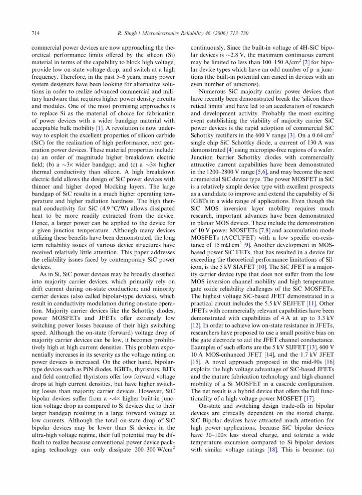
In addition to reliability challenges faced by 4H-SiCMOS devices in the on-state, they must be carefullydesigned in order to ensure good reliability in the reversebias state. Consider an unterminated edge of a PiNdiode with a lateral PiN region supporting the fullblocking voltage, and a metal–oxide–SiC stack adjoin-ing the PN junction, as shown in Fig. 3. For this diodeto support the full voltage capability of SiC, the peakelectric field at the PN junction is close to the criticalelectric field of SiC, which is approximately 2.5 MV/cm. According to Gauss’ law, the electric field in theoxide is the inverse ratio of the dielectric constants,which are 9.7 and 3.9 for SiC and SiO2, respectively.This implies that the electric field in the oxide is
Fig. 3. Unterminated edge of a SiC PiN junction with a metal–oxideand the oxide–semiconductor interface are also shown.
6.2 MV/cm! Termination regions and other activeregions in the devices must be designed carefully to pre-vent a high electric field at the SiC–SiO2 interface.
Note that for reverse biased MOS, the bands bend inthe opposite direction of that shown in Fig. 2, and therelevant barrier height for FN tunneling correspondsto the valence band offset, rather than conduction bandoffset. In contrast to forward biased MOS case, the elec-tric field in the dielectric is determined by its dielectricconstant and interface electric field, rather than thick-ness of the dielectric. The electric field in the oxide isnot excessive in Si-based high voltage devices becausethe critical electric field of Si is about an order of mag-nitude lower than SiC. The high critical electric fieldstrength of SiC can only be utilized to obtain high volt-age SiC devices with SiO2, which has the highest electricfield strength of the commonly studied dielectrics, unlessspecific designs are adopted to alleviate the electric fieldin alternative dielectrics.
The issue of high electric fields in the dielectric is evenmore severe for power MOSFETs in SiC because it isgenerally more difficult to shield gate dielectrics fromhigh electric fields. The three dominant families of Siand SiC power MOSFETs are: DMOSFETs, Trench-gate or UMOSFETs, and lateral MOSFETs. For lateralMOSFETs, the oxide breakdown location is similar tothat shown in Fig. 3. For such MOSFETs [41], a highelectric field exists at the p-base/drift region junction,resulting in a high electric field in the dielectric. In caseof trench gate MOSFETs or UMOSFETs [42], an extre-mely high electric field exists in the oxide at the trenchbottom [43], adjacent to the voltage blocking p-base/ndrift junction, as shown in Fig. 4(a). The electric field
SiC stack beyond the PN junction. The electric fields in the SiC

R. Singh / Microelectronics Reliability 46 (2006) 713–730 719
concentration at the trench corners and the bottom iseven more severe than the lateral case because the trenchbottom must extend below the voltage blocking PNjunction. A smaller pitch worsens rather than alleviatethis problem because it will expose even larger area ofthe trench bottom oxide to high electric field. The elec-tric field at the trench bottom may be lowered to someextent by placing deep p-type extensions below the p-base region [44], in a principle similar to a JBS diode.
The most promising structure for SiC power MOS-FETs may be the DMOSFET structure shown inFig. 4(b), from the standpoint of controlling the electricfield in the gate oxide. The electric field at the SiC–SiO2
interface is lowered by the electric field pinch-off effectfrom the adjacent p-base regions. This leads to a anacceptably low electric field in the gate oxide shownthrough simulations in [45]. However, this pinch-offincreases the resistance of the DMOSFET by introduc-ing a ‘‘JFET’’ region between adjacent p-base regions.The trade-off between the on-state resistance of theDMOSFET and the extent of reduction of electric fieldat the SiC–SiO2 interface is determined by the spacingof the adjacent p-base region, as discussed in detail in[45]. During the evolution of Si DMOSFETs, the reduc-tion in cell pitch resulted in a very high JFET regionresistance. Hence, it was necessary to increase the n-typeconcentration of the JFET region through, for example,n-type ion implantation. For very high voltage SiCDMOSFETs (>2 kV), the lower doping of n-drift regionwill cause the JFET pinch-off to be severe, resulting ina high ‘‘JFET’’ region resistance. However, an n-type
Fig. 4. High electric field location for (a) UMOSFETs and (b) DDMOSFET for the case with and without the JFET region implanta
‘‘JFET’’ implant in SiC DMOSFETs increases the elec-tric field in the oxide to a higher level, as shown inFig. 4(c). This trade-off is less critical for Si DMOSFETsbecause the electric field in the gate oxide for thosedevices is <1 MV/cm due to a lower critical electric fieldof Si.
2.5. Alternative dielectrics for higher reliability?
In contemporary deep submicron Si DRAM devices,alternative dielectrics are being studied [46] to enhancereliability, reduce on-resistance, and have a greater phys-ical thickness versus electrical thickness for the dielec-tric. In order to alleviate some of the reliabilityconcerns, dielectric materials other than SiO2 have beenexplored for the SiC metal–dielectric–semiconductor(MDS) system [47]. Desirable properties for an alterna-tive dielectric that may enhance the performance andreliability of an MDS structure are: (a) low interfacestate density; (b) high dielectric constant; (c) high dielec-tric breakdown strength; and (d) large conduction andvalence band offsets.
For a reverse biased MDS structure, the electric fieldin the dielectric is inversely proportional to its dielectricconstant, and FN tunneling current is exponentiallydependent on the electric field in the dielectric. Thereforefor an identical band offset, the FN current can bereduced dramatically if a dielectric with a slightly higherdielectric constant is utilized. A higher dielectric con-stant also reduces the inversion layer channel resistancesince for a given voltage:
MOSFET power MOS structures. Electric field profile for ation shown in (c).

720 R. Singh / Microelectronics Reliability 46 (2006) 713–730
Rch /tdiel
kdiel
where Rch is the resistance of the channel layer, kdiel isthe dielectric constant, and tdiel is the thickness of thedielectric used to make the MDS channel. A detailedanalysis of the impact of higher dielectric constant(high-k) on the on-resistance of SiC power MOSFETsis discussed in [43]. The reliability of MDS structurescan be increased in the on-state if a thicker dielectric isused to reduce the on-state electric field, at the expenseof the channel resistance. However, depending on thevalue of dielectric constant, the on-resistance may stillbe lower than for SiO2. This allows more flexibility inthe on-state performance/reliability trade-off. This is be-cause, for a dielectric with larger kdiel, a thicker tdiel maybe used for the same Rch.
Although the electric field can be reduced if a high-kdielectric is used for a reverse biased MDS structure, itmust still be lower than its breakdown electric field toprevent its rupture. Unfortunately, based on the analysisof a wide range of high-k semiconductor dielectrics likeSi3N4, Al2O3, HfO2, Ta2O5, ZrO2, La2O3, Pr2O3, TiO2,and SrTiO3 [48], it has been found that the breakdownfield strength decreases as their dielectric constantincreases. Roughly, an empirical relation between EBD
and dielectric constatnt, k is of the form [48]
EBD ¼ 35k�0:64 MV=cm
This may eliminate some dielectrics as possible replace-ments for SiO2 for MDS structures.
What is even more disconcerting is the fact that con-duction band offset of all these dielectrics with respect to4H-SiC is smaller than that of SiC–SiO2 [49], as shownin Fig. 5. A direct replacement of SiO2 with a high-k
dielectric will not achieve a higher reliability because the
200SrTiO3
95Ta2O5
26TiO2
25HfO2
9Al2O3
7.5Si3N4
3.9SiO2
Bre(M
DieleConst
200SrTiO3
95Ta2O5
26TiO2
25HfO2
9Al2O3
7.5Si3N4
3.9SiO2
Bre(M
DielectricConst
Fig. 5. Dielectric constant, breakdown electric field and conductiondielectrics.
primary limitation to reliability of SiC MDS devices is
FN tunneling, which is strongly dependent on the conduc-
tion band offset between SiC and the dielectric. AlthoughAl2O3 offers very attractive properties, it is a difficultmaterial from a device processing standpoint. Somehigh-k materials (like TiO2 and Ta2O5) that were consid-ered promising candidates for replacement of SiO2 in thepast [43,47] have negative conduction band offsets withrespect to 4H-SiC! In general, the bandgap of dielectricsare inversely proportional to their dielectric constants[49]. This is the reason that most materials withhigher-k will also have a smaller conduction and/orvalence band offsets. Although little research has beendone on the SiC–dielectric interface quality for anyhigh-k dielectric, it may be many years before they canmatch the still modest quality of the SiC–SiO2 interface.Hence, it is very unlikely that an alternative dielectricwill replace SiO2 as the dielectric of choice in SiC-basedMDS structure.
One solution to exploit the potential for higher reli-ability and lower on-resistance of high-k dielectrics isto use a stack of dielectrics [45,46]. In this solution, avery thin (5–10 nm) high quality SiO2 layer is in intimatecontact with 4H-SiC, while most of the thickness of gatedielectric is composed of a high-k dielectric. During for-ward bias on this MDS structure, FN tunneling currentcan be lowered because a low electric field is achievedthrough the use of a much thicker high-k material forthe same Rch. As an example, if Si3N4 (k = 7.5) is usedas the high-k dielectric in a SiO2–Si3N4 stack, it can bemade almost 2· thicker than a conventional pure-SiO2
gate dielectric in order to achieve the same Rch. Whilethe conduction band offset is primarily determined bythe SiO2 layer, this 2· reduction in electric field willreduce the FN tunneling quite significantly. Of course,
-0.9?~2.2
-0.4~3
-0.4?~1.5
0.7~6.7
2.013.5
1.610
2.713-15
4H-SiC CoBand Offset (eV)
akdown FldV/cm)
-0.9?~2.2
-0.4~3
-0.4?~1.5
0.7~6.7
2.013.5
1.610
2.713-15
4H-SiC Cond.Band Offset (eV)
akdown FldV/cm)
band offset with respect to 4H-SiC for commonly researched

R. Singh / Microelectronics Reliability 46 (2006) 713–730 721
the thickness of SiO2 should be sufficient so that its con-duction band offset, rather than that of the high-k dielec-tric determines the barrier height for the purposes of FNtunneling. The high-k dielectric should also be chosen sothat its conduction band offset is not too small to influ-ence the FN tunneling properties. The breakdown elec-tric field, dielectric constant and the band offsets oftwo promising candidates for this stacked structure,Si3N4 and Al2O3, are given in Fig. 5. The stacked solu-tion may not offer significantly improved reliability fora reverse biased MDS structure because the electric fieldin the thin oxide is still determined by the electric field atthe SiC–SiO2 interface, and its dielectric constant. How-ever, with appropriate design, the electric field at theSiC–SiO2 interface can be minimized to an acceptablelevel for most devices.
3. Schottky metal-based devices
While the reverse leakage current of PN junction-based devices in principle is largely determined by thebandgap of the semiconductor used, the reverse leakagecurrent for Schottky junctions that are expected to blockthe rated voltage is dependent on the metal–semiconduc-tor barrier height. In some of the most promisingSiC-based power and microwave devices—the powerSchottky diode and the microwave MESFET, a Scho-ttky junction is required to block the rated voltage. Tothe first order, the leakage current in Schottky diodesis given by [34]
J L ¼ A��T 2 exp �UBn
V T
� �
where A** is the modified Richardson constant, T is theoperating temperature, UBn is the metal–semiconductorbarrier height, and VT is the thermal voltage. This equa-tion shows that the leakage current in a voltage-blockingSchottky junction is exponentially dependent on themetal–semiconductor barrier height and the operatingtemperature. Since SiC power Schottky diodes are ex-pected to compete with Si PiN diodes, they must havea comparable forward on-state voltage drop. The mostcommonly used Schottky metals (e.g. titanium and nickel)have UBn values close to Si bandgap value of 1.1 eV[50]. The high temperature blocking performance ofthese Schottky diodes will only approach that on SiPiN diodes, which is in the 125–175 �C range, and notthe 250–350 �C range promised for many PN junction-based devices. The metal–Schottky barrier height is fur-ther reduced due to the effect of barrier height loweringwhen a high reverse electric field is present at the metal–SiC interface during blocking [50]. The presence of mate-rial defects also increases the leakage current in SiCSchottky diodes because these defects act as sites withlower Schottky barrier heights as compared to the bulk
of the device [61]. Since the leakage current is exponen-tially dependent on the Schottky barrier height, evensmall areas with low Schottky barrier heights will con-tribute a significant portion of the leakage current, andwill be even more severely influenced by increasing tem-perature than if a uniform Schottky contacts is assumed[61].
For microwave MESFETs, the limitation of choos-ing a low barrier height metal is not as severe becausethe Schottky contact is in the blocking mode. However,a survey of metal–semiconductor barrier heights in SiC[51] shows that most commonly used metals have Scho-ttky barrier heights in the 1.0–1.9 eV range. Even if thehighest barrier height metal is chosen to form the SiCMESFET, the high temperature performance of thesedevices may not achieve the high temperature promiseof SiC devices. Schottky contacts in MESFETs are pres-ent in channel regions where much higher temperaturesare observed as compared to the bulk of the device. Thistemperature differential can exceed 75 �C [52] becausecurrent densities in the MESFET channel regions canexceed 105 A/cm2! Since gate metal width has to be min-imized for high frequency MESFETs, the choice ofSchottky metal for its formation is limited by the fabri-cation procedures used. It is sometimes difficult tochoose a large Schottky barrier height metal like plati-num and gold because of such limitations. These issueswill limit the operating temperature of SiC Schottky-based devices to silicon-like levels.
4. Materials defect impact on performance and reliability
It is well known that SiC occurs in many polytypes innature, with different bandgaps, carrier mobilities, andcrystal structures. The most commercially relevant poly-types for the manufacture of power devices are 4H-SiCand 6H-SiC [53]. These polytypes offer high breakdownelectric fields (>2 · 106 V/cm), high carrier mobilities,and relative maturity in wafer quality. Presently, thesewafers are commercially available in 3 in (75 mm) diam-eter size with device-grade crystal quality. Larger wafersizes are necessary to reduce the device cost and enablethe widespread adoption of SiC power devices, as exem-plified by other semiconductor technologies.
4.1. Material defects in SiC
The most prominent defect in SiC is the micropipe,and many commercial wafers are graded according tothis specification. A micropipe is a thermodynamicallystable hollow core screw dislocation [53], which showsas a hole through a wafer within a ±15� off the c-axisof the wafer and is close to 1 lm diameter in size. Ithas been shown that a SiC device with a micropipe inits active area cannot support significant electric field

722 R. Singh / Microelectronics Reliability 46 (2006) 713–730
[54], and hence any significant power level. The micro-pipe densities in commercial wafers are steadily decreas-ing as material growth techniques mature, and presentlyit is possible to purchase wafers with a micropipe densityof 5–10 cm�2. However, it is imperative that this ‘killerdefect’ be eliminated in the future for the realization ofhigh current power devices.
Besides micropipes, there are many material defectscommonly observed in present-day SiC. These defectscan be broadly classified into wafer-level defects and epi-taxial defects. Usually SiC wafer defects act as nucleat-ing sites for epitaxial defects that may affect deviceperformance. Various defects on bare SiC wafers are:
1. Closed core screw dislocation (with a typical 1000–5000 cm�2 density) is an ordered crystal defect,similar to a micropipe, that runs continuously oversignificant thickness of wafer. Depending on the epi-taxial growth method, it may continue to grow intothe epitaxial layers. If an active voltage blockingjunction is formed on such a defect, a �20% reduc-tion in critical electric field can be observed [55].These defects may result in a reduction in carrier life-time of epitaxial layers grown over them [56].
2. Basal plane dislocations (typical density: 102–105 cm�2) are islands of single crystal SiC with a dis-placed basal plane which may be annealed usingadvanced epitaxial growth techniques [57].
3. Edge dislocations (104–105 cm�2) are usually one-dimensional defects on the surface of wafers thatget annealed during the epitaxial growth, and rarelyaffect properly designed devices.
4. Low angle boundaries (102–103 cm�2) and polishingdamage found in commercial wafers result inincreased leakage currents during reverse bias opera-tion of the these devices.
Defects in SiC epitaxial layers depend on the meth-ods and reactors used to grow the layers. The most com-mon epitaxial defects are growth pits (1–100 cm�2),triangular inclusions of different polytype (e.g. 3C in4H), carrot (0.1–10 cm�2) and comet tail defects [58].Growth pits and carrot defects result from wafer defectsthat create adverse conditions for the realization of aperfect crystal structure during epitaxial growth. Tem-perature non-uniformities during epitaxial growth causethe appearance of triangle inclusions of different poly-types. Poor management of impurities or prematurenucleations of SiC particulates cause the formation ofcomet tails and other defects.
4.2. Reverse characteristics of SiC devices
When devices are in the reverse blocking mode, i.e.reverse biased Schottky and PN junctions, devices are
expected to have low leakage current and have near-the-oretical blocking voltage. From a reliability perspective,it is important to understand the affect of materials andprocessing defects on leakage current, total blockingvoltage achieved, and sustainable avalanche energyachievable during breakdown. The effect of materialdefects on the device blocking performance has been dis-cussed extensively by Neudeck et al. [56], Kimoto et al.[58] and Lendenmann et al. [59]. The most extensivelystudied defect in SiC is the screw dislocation [60]. Screwdislocations in PN diodes result in a higher leakage cur-rent, a softer breakdown I–V characteristics, and causethe breakdown microplasma to concentrate through thisdefect. Although the leakage current mechanism is dom-inated by this defect, measurements over a 298—673 Ktemperature range show that the leakage current is toler-able in diodes with screw dislocations. The leakage cur-rent near avalanche breakdown voltage is similar indiodes with and without screw dislocations. In fact, apeak avalanche power density of 140 kW/cm2 wasapplied in diodes with screw dislocations with repeatablereverse I–V characteristics. This indicates that a screwdislocation does not cause severe reduction in blockingvoltage of power devices fabricated on them.
Schottky devices (e.g. power Schottky diodes andMESFETs) are very sensitive to surface and morpholog-ical defects. Even small areas with material defects thatcause reduced metal–semiconductor barrier height, candominate reverse blocking characteristics [61]. This isbecause leakage currents in Schottky contacts are expo-nentially dependent on barrier height. Epitaxial growth,which is the main cause of morphological defects, is amuch more important process for reliable and highyielding Schottky devices as compared to PN diodes.However, triangular 3C inclusions are quite devastatingfor blocking properties of both PN and Schottkydevices. They result in >50% reduction in blocking volt-age [56]. Carrots and comet tails result in some increasein leakage currents, but do not cause a severe reductionin blocking voltage. Small growth pits seem to affectSchottky diode more severely than PN junction devices[56]. With the improvement of epitaxial processingthese affects may be minimized for most SiC powerdevices.
4.2.1. Avalanche energy
The pulsed avalanche energy is the amount of energythat the power device can handle safely while it is under-going avalanche breakdown. This energy is determinedby the adiabatic heating of the blocking layer and theintrinsic temperature of this low doped SiC layer. Thestatic avalanche power density of a PN junction madeusing a particular material depends on its density, spe-cific heat, and the temperature at which the intrinsic car-rier density becomes close to the doping density of thevoltage blocking layers (i.e. the bandgap of the mate-

03 4 5 6 7
2
4
6
8
10
Diode Voltage (V)
Fo
rwar
d D
iod
e C
urr
ent
(A)
4H-SiC 0.04 cm2
10 kV PiN Diode
IncreasingDegradation
Fig. 6. On-state characteristics of a high voltage SiC PiNdiodes after various levels of forward bias stress.
R. Singh / Microelectronics Reliability 46 (2006) 713–730 723
rial). Theoretically, the total avalanche energy is calcu-lated to be more than 10· higher than Si devices [62].However, the breakdown current can become dominantover small filaments where all the breakdown micropl-asma is concentrated. This is true for both Si and SiCdevices, and usually, material defects in voltage blockingjunctions initiate these microplasmas. Experimentalresults on SiC PN diodes fabricated show that approxi-mately 5· higher avalanche energy was obtained as com-pared to Si PN devices in steady state.
4.2.2. Blocking stability demonstrations
Early indications of biasing SiC PN junction devicesto their avalanche breakdown limits indicated that SiCdevices may have a negative temperature coefficient ofavalanche breakdown value [62]. However, later experi-mental results conclusively disproved these early obser-vations [63]. Although the cause of the observednegative coefficient of avalanche breakdown was neverconclusively determined, a hypothesis pointed to the roleof crystal defects in this phenomenon. It is possible thatpoor process fabrication conditions used resulted in sur-face contamination or surface states, which led to theseunstable blocking characteristics of SiC diodes.
With rapid introduction of commercial powerdevices, close attention is being paid to reliability ofpower devices under all conditions. The material defectslike micropipes are primary yield limiting factor forthese devices. The first reported reliability testing onSiC Schotttky diodes were made in 1999 by Ruppet al. [64]. In this study, 100 devices with 600 V ratingwere tested for (a) thermal cycling up to 400 �C; (b)cycling between �55 �C and 150 �C for 1000 times; (c)high temperature reverse bias at 150 �C with a reversebias of 600 V for 1000 h; and (d) high humidity, hightemperature reverse bias testing (85 �C, 85% relativehumidity) for 1000 h. None of these tests resulted inany failures. Yield on 600 V, 6 A Schottky diodesexceeded 75% in this report. Recently, another group[65] has also shown a total of 145,000 device-hours ofhigh temperature reverse bias testing, 11,000 device-hours of continuous current ‘‘burn-in’’ testing, and35,000 device-hours of power cycling testing with nofailures.
In a statistically significant study, higher voltage(3.2–4.0 kV) packaged PiN diodes were biased at2250 V under high temperatures (125 �C) for 500 h [55]without showing catastrophic failure. In these devices,the leakage current remained in the 10�8–10�4 A/cm2
range. It is worthwhile to note that in this study, manydevices had a widely varying (factor of 104) level of leak-age currents, but remained stable with time and temper-ature. Although a few diodes showed sporadic increasesin leakage currents, the total leakage current remainedbelow 10�4 A/cm2 range. Many of these variations inleakage currents and their sporadic increases were prob-
ably caused by material and processing defects/variations.
These demonstrations have proven that althoughmaterials defects may cause limitations to yield anddevice performance in the blocking state, they do notresult in severe long term issues with respect to theirblocking reliability and stability. These observed experi-ments are true for both PN and Schottky junctiondevices.
4.3. Forward voltage degradation in SiC PN diodes
While the reverse bias operation of SiC devices havebeen found to be relatively stable, a curious phenome-non observed recently during the forward bias operationof SiC PiN diodes has caused a great deal of concerntowards long term stability of these devices. It has beenobserved that as PN diodes are forward biased for anappreciable length of time, their on-state voltage dropincreased with time, as shown in Fig. 6. The durationover which these devices show this forward bias degra-dation varies from a few milliseconds to many hours[66]. A variation in on-state voltage drop (VF) in PiNdiodes has serious stability concerns because it can resultin current filamentation and local current ‘hogging’. If aportion of the diode has a lower on-state voltage dropthan another region within the same diode due to slightdifferences in material and processing variations, currentwill be diverted into the lower VF region. This can causeexcessive current densities in small portions of the diode,while leaving large portions of it with a low current den-sity, leading to thermal instability of the entire diode.Such characteristics will also prevent safe paralleling ofdevices to boost the total current required for typical

724 R. Singh / Microelectronics Reliability 46 (2006) 713–730
high current applications for which these devices aretargeted.
4.3.1. The observed phenomenon
Optical observation of PN diodes undergoing VF
degradation shows a concomitant formation of a certainmaterial defect in these diodes, as shown in Fig. 7. Prob-ably the first report of this phenomenon, which weretermed as ‘Bright line defects’ since they appear aremobile bright lines, was made by Konstantinov et al.[67]. This was compared to the previously studied for-mation of ‘Dark line defects’ in gallium arsenide lightemitting devices [68], where dislocation growth due tonon-equilibrium carrier injection and crystal strainresults in a similar forward bias degradation phenome-non. Many researchers agree that mobile and propagat-ing crystal stacking faults are the primary cause offorward bias degradation of PN diodes. This defectpropagates through the entire n-base layer. It was ini-tially proposed [69] that the increase in VF is causedby reduced carrier lifetimes due to the formation ofrecombination centers from stacking faults. However,more recent results indicate that the increase in VF
occurs as the stacking faults form a barrier to currentflow and reduce the conduction area. A stacking faultdefect is usually a two-dimensional error in the atomicstacking sequence of a polytype of SiC.
Fig. 8 shows a series of light emission images at var-ious intervals during degradation for two adjacent0.015 cm2 diodes on the same chip. These optical phe-nomena were correlated with a lifetime measurementmethod that uses the turn-off reverse-recovery wave-forms for conditions of high dI/dt and low dV/dt [71].The result of this study indicates that the effective baselifetime is not reduced and the VF degradation is due
Fig. 7. Light emission measurements of a PiN diode before (left) andfaults.
to a reduction in conduction area. Fig. 9(a) and (b) showthe forward bias voltage degradation and reverse recov-ery current for the same diodes as those shown in Figs. 7and 8, where the arrows on Fig. 9(a) and (b) indicate thetime for each frame in Fig. 8(a) and (b), respectively.The rhomboid shaped regions in Fig. 8(a) indicate stack-ing faults emanating from near the surface, presumablyfrom the P–N junction. These stacking faults are nearthe surface by the growth direction and shape as wellas the focal plane of the CCD camera. The devicedegrades rapidly in Fig. 9(a) because the highest excesscarrier concentration is near the P–N junction. The out-lined triangular dark regions in Fig. 8(b) indicate stack-ing faults growing from near the bottom of the driftregion. The white outlines are from partial dislocationsthat bound the stacking faults and the dark regions indi-cate regions where current is reduced. The devicedegrades more slowly at first, as can be seen inFig. 9(b), because the stacking faults are near the bottomof the drift layer where the excess carrier concentrationis lower and the degradation rate increases as the stack-ing faults approach the P–N junction at the surfacewhere the excess carrier concentration is larger.
The fundamental nature, origin and propagation ofthese dislocations have been extensively investigated byvarious researchers [69,70,72]. These defects nucleatefrom existing substrate crystal defects in hexagonal(e.g. 4H and 6H) SiC. The hexagonal crystal structuresof these polytypes of SiC are formed when three distinctatomic patterns are stacked in a particular sequence.This is in contrast with cubic (3C) SiC, which has a fun-damentally two-dimensional structure with only twoatomic patterns stacked together. Hence, 4H-SiC and6H-SiC crystals are metastable at room temperatureand could convert to a locally faulted 3C-like structure
after (right) forward bias stress indicating growth of stacking
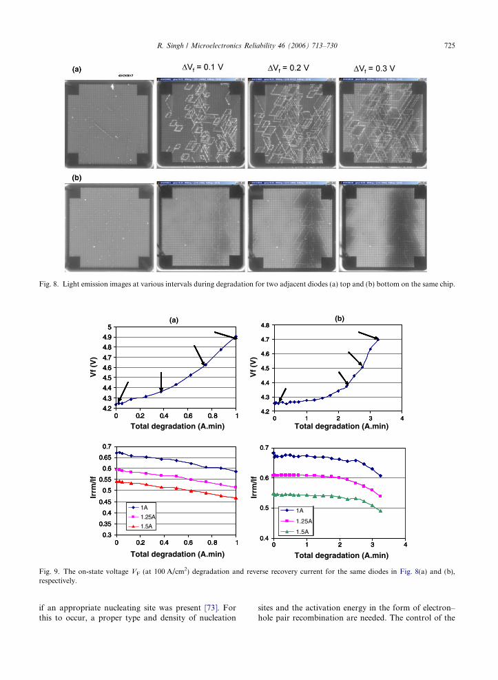
Fig. 8. Light emission images at various intervals during degradation for two adjacent diodes (a) top and (b) bottom on the same chip.
4.2
4.3
4.4
4.5
4.6
4.7
4.8
4.9
5
0 0.2 0.4 0.6 0.8 1
0.3
0.35
0.4
0.45
0.5
0.55
0.6
0.65
0.7
0 0.2 0.4 0.6 0.8 1
1A
1.25A
1.5A
4.2
4.3
4.4
4.5
4.6
4.7
4.8
0 1 2 3 4
0.4
0.5
0.6
0.7
0 1 2 3 4
1A
1.25
1.5A
(a) (b)
4.2
4.3
4.4
4.5
4.6
4.7
4.8
4.9
5
0 0.2 0.4 0.6 0.8 1
0.3
0.35
0.4
0.45
0.5
0.55
0.6
0.65
0.7
0 0.2 0.4 0.6 0.8 1
1A
1.25A
1.5A
4.2
4.3
4.4
4.5
4.6
4.7
4.8
0 1 2 3 4
0.4
0.5
0.6
0.7
0 1 2 3 4
1A
1.25
1.5A
4.2
4.3
4.4
4.5
4.6
4.7
4.8
4.9
5
0 0.2 0.4 0.6 0.8 1
Total degradation (A.min)
Total degradation (A.min)
Total degradation (A.min)
Total degradation (A.min)
Vf
(V)
Vf
(V)
0.3
0.35
0.4
0.45
0.5
0.55
0.6
0.65
0.7
0 0.2 0.4 0.6 0.8 1
Irrm
/If
Irrm
/If
1A
1.25A
1.5A
4.2
4.3
4.4
4.5
4.6
4.7
4.8
0 1 2 3 4
0.4
0.5
0.6
0.7
0 1 2 3 4
1A
1.25A
1.5A
Fig. 9. The on-state voltage VF (at 100 A/cm2) degradation and reverse recovery current for the same diodes in Fig. 8(a) and (b),respectively.
R. Singh / Microelectronics Reliability 46 (2006) 713–730 725
if an appropriate nucleating site was present [73]. Forthis to occur, a proper type and density of nucleation
sites and the activation energy in the form of electron–hole pair recombination are needed. The control of the

3.6
3.7
3.8
3.9
4
4.1
4.2
4.3
4.4
4.5
0 100000 200000 300000 400000 500000
Total Degradation (A.min)
Vf
(V)
Fig. 10. On-voltage VF (at 50 A/cm2) degradation as a functionof total degradation for a 0.5 cm2, 10 kV 4H-SiC PiN diodestressed at 50 A.
0
0.2
3.726 3.926 4.126 4.326 4.526
0.4
0.6
0.8
1
1.2
1.4
1.6
Vf (V)
Irrm
/If
3A
4A
5A
Fig. 11. Correlation between the reverse recovery peak as afunction of total degradation for a 0.5 cm2, 10 kV 4H-SiC PiNdiode.
726 R. Singh / Microelectronics Reliability 46 (2006) 713–730
origin and propagation of these defects may lie in thecontrol of pre-existing defects serving as nucleation sitesfor these defects.
The incidence of propagation of these dislocationswas found to increase with higher current densities[66,73,75]. Higher temperatures and thicker epitaxialthicknesses also resulted in a higher incidence of forma-tion of dislocations. Probe scratches [75], chip scribelines and even silicided contacts on PN diodes are con-sidered to be nucleation sites for mobile and expandingdislocations [74].
4.3.2. Electroluminescence studies and activation energy
of fault generation
Electroluminescence analysis of the emission spectrafound that bright line defects emit light in the red andnear-infrared spectral regions, in contrast to near-band-gap luminescence of non-degraded PN diodes which ispredominantly in the violet region [70]. These defectswere determined to be an irreversible formation of a net-work of linear defects related to crystal dislocations thatsubsequently propagate through, and then beyond thediode area. The nucleating sites for these stacking faultsappear to be primarily at low angle grain boundaries,among other substrate and surface defects. The resultingstacking faults have been observed to be bound bySchockley partial dislocations with a Burger’s vectorb = 1/3h1 0�10i[72]. This implies that the faults propa-gate as triangular or rhombohedral structures with edgesalong the 11–20 directions. These looping structuresmultiply and propagate as the diode is kept in the for-ward bias state. Spectral measurements show that thestacking faults have a primary emission spectrum inthe 450 ± 20 nm peak range [70], and those of threadingdislocations is in the 700 ± 20 nm range. The calculatedactivation energy for the gliding (propagation) of thepartial dislocation that bounds the stacking fault ismeasured to be in the 0.27 ± 0.02 eV range. The esti-mated velocity of propagation of these defects was 7 ·10�5 m/s.
4.3.3. Solutions for VF degradation problem
An activation energy of 0.27 eV is small enough thatmost nucleating sites will result in the formation of thesefaults, and hence some degradation in the on-state volt-age drop of PiN diodes. Hence, the solution for solvingthis problem lies in minimizing the defects in the activeportion of the device. A novel approach to achieving thiswas recently demonstrated by growing Lely crystals withno micropipes and only minimal defects on top of stan-dard substrates [74]. In this experiment, an applicationof 200 A/cm2 stress in the forward direction did not pro-duce any degradation, which was observed with pn junc-tion diodes using normal substrates. Recently, greatstrides have been made in 4H-SiC epitaxy to producePiN structures with relatively stable characteristics by
reducing the material defect density [76]. From thesepreliminary results, it seems that reduction of materialdefects would be directly correlated to obtaining a highyield of drift-free PiN diodes in SiC.
Also, various other methods have been investigatedfor improving the VF degradation [77]. The differentmethods produce different yields of degradation-freedevices with some processes having yields as high as86% degradation-free devices. In each degradation-freeprocess, some devices do not drift at all, while othersdrift a small amount and then stabilize. However, someof the processes also reduce the breakdown voltageyield. Most recently, a new low basal plane dislocation(BPD) process demonstrates substantial increase in theoverall yield with blocking and drift yields of 35% and

R. Singh / Microelectronics Reliability 46 (2006) 713–730 727
67%, respectively [78]. Figs. 10 and 11 show the degrada-tion and monitoring results for a typical low degrada-tion rate 50 A, 10 kV 4H-SiC PiN diode made withthis process.
It is worthwhile to note that such a phenomenon isnot observed in unipolar devices like Schottky diodes,even when the power density (on-current · VF)approaches near levels at which the PN diodes show thisphenomenon [55]. While detailed published reports aremissing, anecdotal data suggests that the forward biasdegradation associated with dislocations occurs in bipo-lar SiC devices like thyristors, GTOs, PiN diodes, andeven bipolar junction transistors (BJTs), but is notobserved in unipolar switches like MOSFETs andJFETs.
5. Conclusions
Despite the remarkable results demonstrated bymany groups around the world in exploiting the supe-rior properties of SiC for high power and high temper-ature devices, there are reliability issues faced by SiC asa material of choice for commercial power devices.Although some of these issues reflect the relative imma-turity of this technology requiring years of develop-ment, some may be fundamental to this material. Anatural oxide–SiO2, is considered a significant advan-tage for realizing a power MOSFET in SiC, whichhas great commercial potential. However, the perfor-mance/reliability trade-off for these devices is moresevere than Si power MOSFETs because of the sub-stantially lower MOS channel mobilities, smaller barrierheight to tunneling, and higher experimentally obtainedinterface state densities. An approach investigated inthis paper is the use of alternative dielectrics withhigher dielectric constants, which may reduce the elec-tric field in SiC MOS devices. However, many of thesematerials suffer from correspondingly lower breakdownfield strength. High breakdown electric field strength ofSiC also affects the choice of passivating dielectrics usedin the edge termination and active regions of powerdevices.
Since the electric fields in dielectrics scale inverselywith their dielectric constants, SiO2 sees a 10· higherelectric field during reverse bias operation of thesedevices, as compared to Si devices. This problem is fur-ther exacerbated in trench-gate MOSFETs because offield crowding at trench corners. This is another motiva-tion for exploring high dielectric constant-high dielectricstrength materials for SiC power devices. The higherbandgap of SiC has often been cited as a reason for pur-suing high temperature power devices because of theircorrespondingly lower leakage currents. However, thereverse leakage currents in Schottky-based devices aredominated by the Schottky barrier height of these mate-
rials. Since the barrier height of commonly usedSchottky metals for SiC devices is in the 0.7–1.2 eVrange, the temperature performance of these devices willbe similar to Si PN junction-based devices. This problemgets very severe in power MESFETs because the gateregions routinely see a much higher local temperature,as compared to the device ambient temperatures.
Material defects in present day SiC are the cause ofmany technological challenges faced by SiC devices.Wafer-level defects include micropipes, closed-corescrew dislocations, basal plane dislocations and lowangle grain boundaries. In the active device regions (epi-taxial layers), some of these defects may be annealed ifgood epitaxial techniques are employed, but othersresult in (a) reduced critical electric field in devices; (b)higher leakage currents during reverse bias operation;and (c) degradation in the on-state performance of bipo-lar devices. Although many of these defects affect thereverse characteristics of high voltage SiC devices, longterm operation of many devices have revealed that opti-mally processed devices do not suffer from reliabilityissues. This has allowed for the commercialization ofthe power SiC Schottky diode. Although the avalancheenergy of SiC power devices is experimentally deter-mined to be 3–10· higher than conventional Si powerdevices material defects have been shown to cause fila-ments that concentrate the plasma of the avalanche cur-rent. Detailed experiments conducted recently onbipolar SiC devices have shown that the on-state voltagedrop in such devices increases with time when they arekept in the forward biased mode for appreciable lengthof time. Optical observation of PN diodes undergoingVF degradation shows a simultaneous formation ofmobile and propagating crystal stacking faults, thatare responsible for a reduction in the diode conductionarea.
Acknowledgements
The author gratefully thanks Dr. Allen R. Hefner ofthe National Institute of Standards and Technology,Gaithersburg, MD for his constant encouragement andsupport in writing this paper. Dr. Hefner’s patienceand enthusiasm were crucial for me to complete thisdocument in this present form. The author furtheracknowledges Dr. Hefner’s entire group at NIST forsharing their experimental data that allowed the verifica-tion of assertions made in this paper.
References
[1] Shenai K, Scott RS, Baliga BJ. Optimum semiconductorsfor high power electronics. IEEE Trans Electron Dev1989;36(9):1811–23.

728 R. Singh / Microelectronics Reliability 46 (2006) 713–730
[2] Singh R. Silicon carbide bipolar power devices—potentialsand limits. In: Materials research society symposiumproceedings, Materials Research Society Fall Meeting,vol. 640, 2001. p. H4.2.1–12.
[3] Stephani D. Status, prospects and commercializationof SiC power devices. In: Proceedings of 59th deviceresearch conference, June 25–27, 2001, Notre Dame, USA.p. 14.
[4] Singh R, Cooper JA, Melloch MR, Chow TP, PalmourJW. SiC power schottky and PiN diodes. IEEE TransElectron Dev 2002;49(4):665–72.
[5] Singh R, Capell DC, Hefner AR, Lai JS, Palmour JW.High power 4H-SiC JBS rectifiers. IEEE Trans ElectronDev 2002;49(11):2054–64.
[6] Dahlquist F, Lendenmann H, Ostling M. A JBS diode withcontrolled forward temperature coefficient and surgecurrent capability. Mater Sci Forum 2002;389–393:1129–32.
[7] Das MK. Recent advances in 4H-SiC MOS device tech-nology. In: Proceedings of international conference onsilicon carbide and related materials (ICSCRM 2003),Lyon, France, October 5–10. p. 62.
[8] Ryu S-H, Agarwal A, Richmond JT, Palmour JW.Development of 10 kV 4H-SiC power MOSFET. In:Proceedings of international conference on silicon carbideand related materials (ICSCRM 2003), Lyon, France.October 5–10. p. 47.
[9] Singh R, Capell DC, Richmond JT, Palmour JW. Highchannel density, 20 A 4H-SiC ACCUFET withRon,on,sp = 15 mX cm2. IEE Electron Lett 2003;39(1):152–4.
[10] Sugawara Y, Asano K, Takayama D, Ryu S, Singh R,Palmour J, Hayashi T. 5.0 kV 4H-SiC SEMOSFETwith low Rons of 88 mX cm2. International Con-ference on silicon carbide and related materials(ICSCRM2001). Mater Sci Forum 2002;389–393(2):1199–202.
[11] Asano K, Sugawara Y, Ryu S, Singh R, Palmour J,Hayashi T, Takayama D. 5.5 kV normally-off low RonS4H-SiC SEJFET. In: Proceedings of 2001 internationalsymposium on power semiconductor devices & ICs, Osaka,Japan, June 4–7, 2001. p. 23–6.
[12] Friedrichs P, Mitlehner H, Schorner R, Dohnke KO,Elpelt R, Stephani D. Application oriented unipolar switch-ing SiC devices. Mater Sci Forum 2002;389–393(2):1185–90.
[13] Sugawara Y, Takayama D, Asano K, Ryu S, Miyauchi A,Ogata S, and Hayashi T. 4H-SiC high power SIJFETmodule. In: Proceedings of the 15th international sympo-sium on power semiconductor devices and ICs, 2003. p.127–30.
[14] Chang H-R, Hanna E, Radun AV. Development anddemonstration of silicon carbide (SiC) inverter module inmotor drive. In: Proceedings of the 15th internationalsymposium on power semiconductor devices and ICs,2003. p. 131–4.
[15] Zhao JH, Tone K, Li X, Alexandrov P, Fursin L, WeinerM. 3.6 mX-cm2, 1726 V normally-off trenched, andimplanted vertical JFETs. In: Proceedings of the 15thinternational symposium on power semiconductor devicesand ICs, 2003. p. 50 –3.
[16] Baliga BJ. Trends in power semiconductor devices. IEEETrans Electron Dev 1996;43(10):1717–31.
[17] Friedrichs P, Mitlehner H, Schorner R, Dohnke KO,Elpelt R, Stephani D. Stacked high voltage switch based onSiC VJFETs. In: Proceedings of the 15th internationalsymposium on power semiconductor devices and ICs,2003. p. 139–143.
[18] Singh R, Irvine KG, Capell DC, Richmond JT, Berning D,Hefner AR, et al. Large area, ultra-high voltage 4H-SiCp–i–n rectifiers. IEEE Trans. Electron Dev. 2002;49(12):2308–16.
[19] Sugawara Y, Takayama D, Asano K, Singh R, Palmour J,Hayashi T. 12-19 kV 4H-SiC pin diodes with low powerloss. In: Proceedings of the 13th international symposiumon power semiconductor devices and ICs, 2001. p. 27–30.
[20] Singh R, Capell DC, Irvine KG, Richmond JT, PalmourJW. 7.4 kV, 330 A (pulsed) single chip, high temperature4H-SiC pin rectifiers. IEE Electron Lett2002;38(25):1738–40.
[21] Sugawara Y, Takayama D, Asano K, Singh R, KodamaH, Ogata S, Hayashi T. 3 kV 600 A 4H-SiC high temper-ature diode module. In: Proceedings of the 14th interna-tional symposium on power semiconductor devices andICs, 2002. p. 245–8.
[22] Palmour JW, Singh R, Waltz DG. High power 4H-SiCthyristors. In: Proceedings of the 54th device researchconference, Santa Barbara, USA, 1996. p. 54–5.
[23] Sugawara Y. Recent progress in SiC power device devel-opments and application studies. In: Proceedings of the15th international symposium on power semiconductordevices and ICs, 2003. p. 10–8.
[24] Ryu S-H, Agarwal AK, Singh R, Palmour JW. 3100 V,asymmetrical, gate turn-off (GTO) thyristors in 4H-SiC.IEEE Electron Dev Lett 2001;22(3):127–9.
[25] Ryu S-H, Agarwal AK, Singh R, Palmour JW. 1800 VNPN bipolar junction transistors in 4H-SiC. IEEE Elec-tron Dev Lett 2001;22(3):124–6.
[26] Huang C-F. 4H-SiC NPN bipolar junction transistors withBVCEO > 3200 V. In: Proceedings of the 14th internationalsymposium on power semiconductor devices and ICs,2002. p. 57–60.
[27] Singh R, Ryu Sei-Hyung, Capell DC, Palmour JW. HighTemperature SiC Trench gate p-IGBTs. IEEE TransElectron Dev 2003;50(3):774–84.
[28] Singh R, Irvine KG, Palmour JW. 4H-SiC buried gate fieldcontrol thyristor. In: Proceedings of the 55th deviceresearch conference, June 23–25, Ft. Collins, USA, 1997.p. 34–5.
[29] Neudeck PG, Petit JB, Salupo CS. Silicon carbide buried-gate junction field effect transistors for high-temperaturepower electronic applications. In: Transactions secondinternational high temperature electronic conference heldin Charlotte NC, published by Sandia National Labora-tories, Albuquerque NM, 1994. p. X-23–8.
[30] Alexandrov P, Zhao JH, Wright W, Pan M, Weiner M.Demonstration of 140 A, 800 V 4H-SiC pin/Schottkybarrier diodes with multi-step junction termination exten-sion structures. IEE Electron Lett 2001;37(18):1139–40.
[31] Afanasev VV, Bassler M, Pensl G, Schulz MJ. Band offsetsand electronic structure of SiC/SiO2 interfaces. J Appl Phys1996;79(6):3108–14.

R. Singh / Microelectronics Reliability 46 (2006) 713–730 729
[32] Pananakakis G, Ghibaudo G, Kies R. Temperature depen-dence of the Fowler–Nordheim current in metal–oxide–degenerate structures. J Appl Phys 1995;78(4): 2635–41.
[33] http://public.itrs.net/.[34] Sze SM. Physics of semiconductor devices. New York:
John Wiley & Sons; 1981.[35] Chung GY, Tin CC, Williams JR, McDonald K, Di Ventra
M, Pantelides ST, et al. Effect of nitric oxide annealing onthe interface trap densities near the band edges in the4Hpolytype of silicon carbide. Appl Phys Lett 2000;76(13):1713–5.
[36] Afanasev VV, Bassler M, Pensl G, Schultz M. IntrinsicSiC/SiO2 interface states. Phys Status Solidi (a)1997;162:321.
[37] Ouisse T, Bano E. Electronic properties of the SiC–SiO2
interface and related systems. In: Proceedings of thesemiconductor interface specialist conference, Charleston,SC, 1997. p. 101–10.
[38] Schorner R, Friedrichs P, Peters D, Stephani D. Signifi-cantly improved performance of MOSFETs on siliconcarbide using the 15R-SiC polytype. IEEE Electron DevLett 1999;20:241.
[39] Li, H-f, Dimitrijev S, Sweatman D, Harrison HB. Analysisof Fowler–Nordheim injection in NO Nitrided gate oxidegrown on n-type 4H-SiC. In: Proceedings of the 22ndinternational conference on microelectronics (MIEL 2000),vol. 1, Nis, Serbia, 2000. p. 331–3.
[40] Chanana RK, McDonald K, Ventra MD, Pantelides ST,Chung GY, Tin CC, et al. Fowler–Nordheim hole tunnel-ing in p-SiC/SiO2 structures. Appl Phys Lett2000;77(16):2560–2.
[41] Banerjee S, Chow TP, Gutmann RJ. 1300 V 6H-SiC lateralMOSFETs with two RESURF zones. IEEE Electron DevLett 2002;23(10):624–6.
[42] Palmour JW, Singh R, Lipkin LA, Waltz DG. 4H-siliconcarbide high temperature power devices. In: Proceedings ofthe third international high temperature electronics con-ference (HiTEC), Albuquerque, New Mexico, USA, June9–14, 1996.
[43] Sridevan S, McLarty PK, Baliga BJ. Analysis of gatedielectrics for SiC power UMOSFETs. In: Proceedings ofthe international power semiconductor devices and IC’s(ISPSD), 26–29 May 1997. p. 153–6.
[44] Singh R, Palmour JW. Silicon carbide metal–insulatorsemiconductor field effect transistor. US Patent 5,719,409,February 17, 1998.
[45] Singh R, Capell DC, Das MK, Lipkin LA, Palmour JW.Development of high current 4H-SiC ACCUFET. IEEETrans Electron Dev 2003;50(2):471–8.
[46] Wallace RM, Wilk G. High-k gate dielectric materials.MRS Bull 2002(March):192–7.
[47] Lipkin LA, Palmour JW. Insulator investigation on SiC forimproved reliability. IEEE Trans Electron Dev 1999;46(3):525–32.
[48] McPherson JW, Kim J, Shanware A, Mogul H, RodriguezJ. Trends in the ultimate breakdown strength of highdielectric constant materials. IEEE Trans Electron Dev2003;50(8):1771–8.
[49] Robertson J. Electronic structure and band offsets of highdielectric constant gate oxides. MRS Bull 2002(March):217–21.
[50] Crofton J, Sriram S. Reverse leakage current calculationsfor SiC Schottky contacts. IEEE Trans Electron Dev1996;43(12):2305–7.
[51] Itoh A, Takemura O, Kimoto T, Matsunami H. Inst PhysConf Ser 1996;142:685.
[52] Royet AS, Ouisse T, Cabon B, Noblanc O, Arnodo C,Brylinski C. Self heating effects in silicon carbideMESFETs. IEEE Trans Electron Dev 2000;47(11):2221–7.
[53] Palmour JW, Singh R, Glass RC, Kordina O, Carter Jr.,CH. Silicon carbide for power devices. In: IEEE interna-tional symposium on power semiconductor devices andIC’s, ISPSD, 1997. p. 25–32.
[54] Neudeck PG, Powell JA. Performance limiting micropipedefects in silicon carbide wafers. IEEE Electron Dev Lett1994;15(2):63–5.
[55] Lendenmann H, Dahlquist F, Johansson N, Soderholm R,Nilsson PA, Bergman JP, et al. Long term operation of4.5 kV PiN and 2.5 kV JBS diodes. Mater Sci Forum2001;353–356:727–30.
[56] Neudeck PG. Electrical impact of SiC structural crystaldefects on high electric field devices. Mater Sci Forum2000;338–342:1161–6.
[57] Kordina O, Hallin C, Glass RC, Henry A, and Janzen E. Anovel hot-wall CVD reactor for SiC epitaxy. In: Siliconcarbide and related materials, Institute of Physics Confer-ence Series No. 137, 1994. p. 41.
[58] Kimoto T, Miyamoto N, Matsunami H. Performancelimiting surface defects in SiC epitaxial layers p–n junctiondiodes. IEEE Trans Electron Dev 1999;46(3):471–7.
[59] Lendenmann H, Dahlquist F, Bergman JP, Bleichner H,Hallin C. High power SiC diodes—characteristics, reliabil-ity and relation to material defects. Mater Sci Forum2002;389–393:1259–64.
[60] Neudeck PG, Huang W, Dudley M. Study of bulk andelementary screw dislocation assisted reverse breakdown inlow-voltage (<250 V) 4H-SiC P + N junction diodes—PartI: DC properties. IEEE Trans Electron Dev 1999;46(3):478–84.
[61] Bhatnagar M, Baliga BJ, Kirk HR, Rozgonyi GA. Effectof surface inhomogeneities on the electrical characteristicsof SiC Schottky contacts. IEEE Trans Electron Dev1996;43(1):150–6.
[62] Neudeck PG, Fazi C. Study of bulk and elementary screwdislocation assisted reverse breakdown in low-voltage(<250 V) 4H-SiC P + N junction diodes—Part II: Dynamicbreakdown properties. IEEE Trans Electron Dev1999;46(3):485–92.
[63] Neudeck PG. Positive temperature coefficient of break-down voltage in 4H-SiC PN junction rectifiers. IEEEElectron Dev Lett 1997;18(3):96–8.
[64] Rupp R, Treu M, Mauder A, Griebl E, Werner W, BartschW, et al. Performance and reliability issues of SiC-Scho-ttky diodes. Mater Sci Forum 2000;338–342:1167–70.
[65] http://www.cree.com/ftp/pub/PETECH2002_paper_SiC/Schottky.pdf.
[66] Stahlbush RE, Fedison JB, Arthur SD, Rowland LB,Kretchmer JW, Wang S. Propagation of current inducedstacking faults and forward voltage degradation in 4H-SiCPiN diodes. Mater Sci Forum 2002;389–393:427–30.
730 R. Singh / Microelectronics Reliability 46 (2006) 713–730
[67] Konstantinov AO, Bleichner H. Bright-line defect forma-tion in silicon carbide injection diodes. J Appl Phys1997;71(25):3700–2.
[68] Maeda K, Suzuki K, Ichihara M. Microsc MicroanalMicrostruct 1993;4:211.
[69] Bergman JP, Lendenmann H, Nilsson PA, Lindefelt U,Skytt P. Crystal defects as source of anomalous forwardvoltage increase of 4H-SiC diodes. Mater Sci Forum2001;353–356:299–302.
[70] Galeckas A, Linnros L, Pirouz P. Recombination-enhanced extension of stacking faults in 4H-SiC p–i–ndiodes under forward bias. Appl Phys Lett 2002;81(5):883–5.
[71] Hefner A. IEEE Trans Ind Appl 1994;30:394.[72] Skowrownski M, Liu JQ, Vetter WM, Dudley M, Hallin C,
Lendenmann H. Recombination-enhanced defect motionin forward-biased 4H-SiC p–n diodes. J Appl Phys2002;92(8):4699–704.
[73] Ha S, Chung HJ, Skowrownski M, Sumakeris JJ. Solidstate transformations of hexagonal SiC polytypes.Abstracts of International Symposium on Silicon Carbideand Related Materials 2003. Lyons, France.
[74] Tanaka Y, Nishizawa S, Fukuda K, Arai K, Ohno T,Oyanagi N, et al. Fabrication of 1.4 kV mesa-type p+–ndiodes with avalanche breakdown and without forwarddegradation on high-quality 6H-SiC substrates. Appl PhysLett 2003;83(2):377–9.
[75] Lendenmann H. Forward degradation in bipolar SiCdevices: phenomenon, defect origins, and device effects.In: ONR Workshop on extended defects in wide band gapsemiconductors: electrical and optical effects, Belize, 27–31January 2002.
[76] Das MK, Sumakeris JJ, Paisely MJ, Power AR. Highpower 4H-SiC PiN diodes with minimal forward voltagedrift. In: Proceedings of the international conference onsilicon carbide and related materials (ICSCRM 2003),Lyon, France. October 5–10. p. 65–6.
[77] Sumakeris JJ, et al. Approaches to stabilizing the forwardvoltage of bipolar devices. In: International conference onsilicon carbide and related materials, Lyon, France, Octo-ber 2003.
[78] Mrinal K. Das, et al., Drift-free, 50 A, 10 kV 4H-SiC PiNdiodes with improved device yields. In: Proceedings ofECSCRM Bologna, Italy, 2004.