red box rules are for proof stage only....
TRANSCRIPT

Silicon
Pho
ton
icsFundam
entals and Devices
Wiley Series in Materials for Electronic & Optoelectronic Applications
DeenBasu
SiliconPhotonicsFundamentalsand Devices
M. Jamal Deenand P. K. Basu
M. Jamal DeenDepartment of Electrical and Computer Engineering, McMaster University, Canada
P. K. BasuInstitute of Radiophysics and Electronics, University of Calcutta, India
The creation of affordable high speed optical communications using standard semiconductor manufacturing technology is a principal aim of silicon photonics research. This would involve replacing copper connections with optical fibres or waveguides, and electrons with photons. With applications such as telecommunications and information processing, light detection, spectroscopy, holography and robotics, silicon photonics has the potential to revolutionise electronic-only systems. Providing an overview of the physics, technology and device operation of photonic devices using exclusively silicon and related alloys, the book includes:n Basic Properties of Siliconn Quantum Wells, Wires, Dots and Superlatticesn Absorption Processes in Semiconductorsn Light Emitters in Siliconn Photodetectors, Photodiodes and Phototransistors n Raman Lasers including Raman Scatteringn Guided Lightwavesn Planar Waveguide Devicesn Fabrication Techniques and Material Systems
Silicon Photonics: Fundamentals and Devices outlines the basic principles of operation of devices, the structures of the devices, and offers an insight into state-of-the-art and future developments.
Fundamentalsand Devices
SiliconPhotonics
Series EditorsArthur Willoughby, University of Southampton, Southampton, UKPeter Capper, SELEX Galileo Infrared Ltd, Southampton, UKSafa Kasap, University of Saskatchewan, Saskatoon, Canada. . . . . . . . . . . . . . . . . . . . . . . . . . . . . . . . . . . . . . . . . . . . . . . . . . . . . . . . . . . . . . . . . . . . . . . . . . . . . . . . . . . . . . . . . . . . .
RED BOX RULES ARE FOR PROOF STAGE ONLY. DELETE BEFORE FINAL PRINTING. PPC FINAL AW


Silicon Photonics

Wiley Series in Materials for Electronic and Optoelectronic Applications
www.wiley.com/go/meoa
Series Editors
Professor Arthur Willoughby, University of Southampton, Southampton, UK
Dr Peter Capper, SELEX Galileo Infrared Ltd, Southampton, UK
Professor Safa Kasap, University of Saskatchewan, Saskatoon, Canada
Published Titles
Bulk Crystal Growth of Electronic, Optical and Optoelectronic Materials,
Edited by P. Capper
Properties of Group-IV, III – V and II – VI Semiconductors, S. Adachi
Charge Transport in Disordered Solids with Applications in Electronics,
Edited by S. Baranovski
Optical Properties of Condensed Matter and Applications, Edited by J. Singh
Thin Film Solar Cells: Fabrication, Characterization and Applications,
Edited by J. Poortmans and V. Arkhipov
Dielectric Films for Advanced Microelectronics, Edited by M. R. Baklanov, M. Green
and K. Maex
Liquid Phase Epitaxy of Electronic, Optical and Optoelectronic Materials, Edited by P. Capper
and M. Mauk
Molecular Electronics: From Principles to Practice, M. Petty
CVD Diamond for Electronic Devices and Sensors, Edited by R. S. Sussmann
Properties of Semiconductor Alloys: Group-IV, III – V and II – VI Semiconductors, S. Adachi
Mercury Cadmium Telluride, Edited by P. Capper and J. Garland
Zinc Oxide Materials for Electronic and Optoelectronic Device Applications,
Edited by C. Litton, D.C. Reynolds and T. C. Collins
Forthcoming Titles
Lead-Free Solders: Materials Reliability for Electronics, Edited by K. N. Subramanian
Nanostructured Waveguides: Fundamentals and Applications, M. Skorobogatiy

Silicon PhotonicsFundamentals and Devices
M. JAMAL DEEN
Department of Electrical and Computer Engineering,McMaster University, Canada
P. K. BASU
Institute of Radiophysics and Electronics,University of Calcutta, India

This edition first published 2012
� 2012 John Wiley & Sons Ltd
Registered office
John Wiley & Sons Ltd, The Atrium, Southern Gate, Chichester, West Sussex, PO19 8SQ, United Kingdom
For details of our global editorial offices, for customer services and for information about how to apply for permission
to reuse the copyright mat erial in this book please see our website at www.wiley.com.
The right of the author to be identified as the author of this work has been asserted in accordance with the Copyright,
Designs and Patents Act 1988.
All rights reserved. No part of this publication may be reproduced, stored in a retrieval system, or transmitted, in any form
or by any means, electronic, mechanical, photocopying, recording or otherwise, except as permitted by the UK Copyright,
Designs and Patents Act 1988, without the prior permission of the publisher.
Wiley also publishes its books in a variety of electronic formats. Some content that appears in print may not be available
in electronic books.
Designations used by companies to distinguish their products are often claimed as trademarks. All brand names and
product names used in this book are trade names, service marks, trademarks or registered trademarks of their respective
owners. The publisher is not associated with any product or vendor mentioned in this book. This publication is designed
to provide accurate and authoritative information in regard to the subject matter covered. It is sold on the understanding
that the publisher is not engaged in rendering professional services. If professional advice or other expert assistance
is required, the services of a competent professional should be sought.
The publisher and the authormake no representations orwarrantieswith respect to the accuracy or completeness of the contents of
this work and specifically disclaim all warranties, including without limitation any implied warranties of fitness for a particular
purpose. This work is sold with the understanding that the publisher is not engaged in rendering professional services. The advice
and strategies contained herein may not be suitable for every situation. In view of ongoing research, equipment modifications,
changes in governmental regulations, and the constant flow of information relating to the use of experimental reagents,
equipment, and devices, the reader is urged to review and evaluate the information provided in the package insert or instructions
for each chemical, piece of equipment, reagent, or device for, among other things, any changes in the instructions or indication
of usage and for added warnings and precautions. The fact that an organization or Website is referred to in this work as a citation
and/or a potential source of further information does not mean that the author or the publisher endorses the information the
organization or Website may provide or recommendations it may make. Further, readers should be aware that Internet Websites
listed in this workmay have changed or disappeared betweenwhen this workwaswritten andwhen it is read. Nowarrantymay be
created or extended by any promotional statements for this work. Neither the publisher nor the author shall be liable for any
damages arising herefrom.
Library of Congress Cataloging-in-Publication Data
Deen, M. Jamal.
Silicon photonics : fundamentals and devices / M.J. Deen, P.K. Basu.
p. cm.
Includes bibliographical references and index.
ISBN 978-0-470-51750-5 (cloth)
1. Silicon–Optical properties. 2. Optoelectronic devices. 3. Photonics.
I. Basu, P. K. (Prasanta Kumar) II. Title.
TA1750.D44 2012
621.381502–dc232011050047
A catalogue record for this book is available from the British Library.
Print ISBN: 9780470517505
Set in 10/12pt Times Roman by Thomson Digital, Noida, India
Printed in [Country] by [Printer]

Dedication
PKBTo Chitrani (wife), Rikmantra (son), and Kaberi (sister)
MJDTo Meena (wife), and Arif, Imran, and Tariq (sons)


Contents
Series Preface xvPreface xvii
1 Introduction to Silicon Photonics 1
1.1 Introduction 1
1.2 VLSI: Past, Present, and Future Roadmap 2
1.3 The Interconnect Problem in VLSI 3
1.4 The Long-Haul Optical Communication Link 5
1.4.1 Basic Link and Components 5
1.4.2 Materials and Integration 7
1.5 Data Network 8
1.6 Conclusions 8
1.7 Scope of the Book 9
References 11
2 Basic Properties of Silicon 13
2.1 Introduction 13
2.2 Band Structure 14
2.2.1 E–k Diagram: General Considerations 14
2.2.2 Band Properties near Extremas 16
2.2.3 Refined Theory for Band Structures 17
2.2.4 Temperature- and Pressure-Dependent Band Gap 18
2.2.5 Band Structure in Ge 18
2.3 Density-of-States Function 19
2.4 Impurities 22
2.4.1 Donors and Acceptors 22
2.4.2 Isoelectronic Impurities 23
2.5 Alloys of Silicon and Other Group IV Elements 24
2.5.1 Different Alloy Systems 24
2.5.2 Lattice Constants 24
2.5.3 Band Structures of Unstrained Alloys 25
2.6 Heterojunctions and Band Lineup 26
2.7 Si-Based Heterostructures 27
2.7.1 Lattice-Mismatched Heteroepitaxy 27
2.7.2 Pseudomorphic Growth and Critical Thickness 28
2.7.3 Elasticity Theory: Stress and Strain 28
2.7.4 Expressions for Critical Thickness 30
2.7.5 Strain Symmetric Structures and Virtual Substrates 31

2.7.6 Band Offsets and Band Lineup 32
2.7.7 Electronic Properties of SiGe/Si Heterostructures 36
2.8 Direct Gap: Ge/SiGeSn Heterojunctions 39
2.8.1 Structures 39
2.8.2 Band Edges and Band Lineup 40
Problems 42
References 44
Suggested Readings 45
3 Quantum Structures 473.1 Introduction 47
3.2 Quantum Wells 47
3.2.1 Condition for Quantum Confinement 48
3.2.2 A Representative Structure 48
3.2.3 Simplified Energy Levels 49
3.2.4 Density-of-States in Two Dimensions 52
3.2.5 Finite Quantum Well 53
3.2.6 Refined Methods 54
3.2.7 Different Band Alignments 55
3.3 Quantum Wires and Dots 55
3.3.1 Subbands and DOS in Quantum Wires 56
3.3.2 Quantum Dots 57
3.4 Superlattices 58
3.5 Si-Based Quantum Structures 59
3.5.1 Electron Subband Structure 59
3.5.2 Hole Subbands 62
3.5.3 Quantum Wells and Barriers 62
3.6 Effect of Electric Field 63
Problems 65
References 67Suggested Readings 67
4 Optical Processes 69
4.1 Introduction 69
4.2 Optical Constants 69
4.3 Basic Concepts 73
4.3.1 Absorption and Emission 73
4.3.2 Absorption and Emission Rates 73
4.4 Absorption Processes in Semiconductors 74
4.5 Fundamental Absorption in Direct Gap 75
4.5.1 Conservation Laws 75
4.5.2 Calculation of Absorption Coefficient 76
4.6 Fundamental Absorption in Indirect Gap 82
4.6.1 Theory of Absorption 83
4.6.2 Absorption Spectra in Si 85
4.6.3 Absorption Spectra in Ge 86
viii Contents

4.7 Absorption and Gain 86
4.8 Intervalence Band Absorption 89
4.9 Free-carrier Absorption 89
4.10 Recombination and Luminescence 92
4.10.1 Luminescence Lifetime 92
4.10.2 Carrier Lifetime: Dependence on Carrier Density 94
4.10.3 Absorption and Recombination 95
4.10.4 Microscopic Theory of Recombination 96
4.11 Nonradiative Recombination 97
4.11.1 Recombination via Traps 97
4.11.2 Auger Recombination 100
4.11.3 Surface Recombination 101
4.11.4 Recombination of Complexes 102
4.12 Excitonic and Impurity Absorption 102
4.12.1 Excitons 102
4.12.2 Impurity 104
4.12.3 Bound Excitons 104
4.12.4 Isoelectronic Centres 105
Problems 105
References 107
5 Optical Processes in Quantum Structures 109
5.1 Introduction 109
5.2 Optical Processes in QWs 110
5.2.1 Absorption in Direct-gap QW 110
5.2.2 Gain in QW 112
5.2.3 Recombination in QWs 112
5.2.4 Polarization-Dependent Momentum Matrix Element 113
5.2.5 Absorption in the Indirect Gap 114
5.2.6 Absorption in Type II QWs 117
5.3 Intersubband Transitions 118
5.3.1 Conduction Subbands: Isotropic Mass 119
5.3.2 Anisotropic Mass 120
5.3.3 Intervalence Band Absorption 122
5.4 Excitonic Processes in QWs 122
5.4.1 Excitons in 2D: Preliminary Concepts 122
5.4.2 Excitons in Purely 2D Systems 123
5.4.3 Excitonic Absorption in Direct-gap QWs 125
5.4.4 Excitonic Processes in Indirect-gap QWs 126
5.4.5 Photoluminescence in QWs 127
5.5 Effect of Electric Fields 127
5.5.1 Qualitative Discussion of Electroabsorption 128
5.5.2 Electroabsorption and Electrorefraction in SiGe QWs 129
5.6 Optical Processes in QWRs 132
5.7 Optical Processes in QDS 133
Problems 135
References 136
Contents ix

6 Light Emitters in Si 139
6.1 Introduction 139
6.2 Basic Theory of Light Emission 140
6.3 Early Efforts: Zone Folding 142
6.4 Band Structure Engineering Using Alloys 143
6.5 Quantum Confinement 145
6.5.1 Quasi-direct No-phonon Transition 146
6.5.2 Porous Si 148
6.5.3 Silicon Nanocrystals 149
6.5.4 Quantum Wells, Wires, and Dots 151
6.6 Impurities in Silicon 152
6.6.1 Isoelectronic Impurities 152
6.6.2 Rare-earth Luminescence 152
6.7 Stimulated Emission: Prospect 157
6.7.1 Si Nanocrystals 157
6.7.2 Bulk Si 159
6.8 Intersubband Emission 161
6.8.1 Emission at Mid-infrared 163
6.8.2 Terahertz Emission 163
6.9 Tensile-Strained Ge Layers 165
Problems 167
References 167
7 Si Light Modulators 171
7.1 Introduction 171
7.2 Physical Effects 172
7.2.1 Electroabsorption and Electrorefraction 173
7.2.2 Electro-Optic Effect 173
7.2.3 Franz–Keldysh Effect 175
7.2.4 Quantum-Confined Stark Effect 175
7.2.5 Carrier-Induced Effects 176
7.2.6 Thermo-Optic Effect 176
7.3 Electrorefraction in Silicon 177
7.3.1 Electro-Optic Effects 177
7.3.2 Carrier Effect 177
7.3.3 Quantum Confined Stark Effect 179
7.4 Thermo-Optic Effects in Si 179
7.5 Modulators: Some Useful Characteristics 180
7.5.1 Modulation Depth 180
7.5.2 Modulation Bandwidth 180
7.5.3 Insertion Loss 181
7.5.4 Power Consumption 181
7.5.5 Isolation 181
7.6 Modulation Bandwidth under Injection 182
7.7 Optical Structures 183
7.7.1 MZI 183
7.7.2 Fabry–Perot Resonator 184
x Contents

7.7.3 MZI versus a Resonator 185
7.8 Electrical Structures 186
7.8.1 p–i–n Structures 186
7.8.2 Three-Terminal Structures 188
7.8.3 Smaller Structures 188
7.8.4 MOS Capacitors 189
7.8.5 MQW Structures 190
7.9 High-Bandwidth Modulators 190
7.9.1 Ring Resonator 190
7.9.2 MZ Modulators at 10 Gb/s and Above 191
7.9.3 Microring Resonators 192
7.9.4 Reverse Biased p–n Diode 193
7.10 Performance of EO Modulators 193
Problems 193
References 194
8 Silicon Photodetectors 197
8.1 Introduction 197
8.2 Optical Detection 199
8.3 Important Characteristics of Photodetectors 202
8.3.1 Quantum Efficiency 202
8.3.2 Responsivity 204
8.3.3 Bandwidth 206
8.3.4 Gain 206
8.3.5 Noise and Noise-Equivalent Power 206
8.3.6 Wavelength Sensitivity Range 209
8.3.7 Cost and Yield 209
8.3.8 Other Characteristics 210
8.4 Examples of Types of Photodetectors 210
8.5 Examples of Photodiodes in Standard
Silicon Technology 216
8.6 Phototransistors in Standard Silicon Technology 221
8.7 CMOS and BiCMOS 223
8.8 Silicon-on-Insulator (SOI) 223
8.9 Photodetectors Using Heteroepitaxy 227
8.9.1 Si and SiGe Multiple Quantum Wells 227
8.9.2 Ge Detectors on Si 232
8.9.3 Related Theoretical Discussion 239
Problems 242
References 244
9 Raman Lasers 2499.1 Introduction 249
9.2 Raman Scattering: Basic Concepts 250
9.2.1 Stokes and Anti-Stokes Lines 250
9.2.2 Stimulated Raman Scattering 252
Contents xi

9.3 Simplified Theory of Raman Scattering 252
9.4 Raman Effect in Silicon 255
9.5 Raman Gain Coefficient 256
9.5.1 Mathematical Model 256
9.5.2 Simulation Parameters 257
9.5.3 Threshold Power 257
9.6 Continuous-Wave Raman Laser 259
9.7 Further Developments 262
Problems 262
References 263
10 Guided Lightwaves: Introduction 265
10.1 Introduction 265
10.2 Ray Optic Theory for Light Guidance 265
10.3 Reflection Coefficients 266
10.4 Modes of a Planar Waveguide 268
10.4.1 The Symmetrical Planar Waveguide 269
10.4.2 The Asymmetric Waveguide 270
10.4.3 Single-Mode Condition 270
10.4.4 Effective Index of a Mode 271
10.5 Wave Theory of Light Guides 271
10.5.1 Wave Equation in a Dielectric 271
10.5.2 The Ideal Slab Waveguide 272
10.6 3D Optical Waveguides 278
10.6.1 Practical Waveguiding Geometries 278
10.6.2 Ray Optic Approach for 3D Guides 281
10.6.3 Approximate Analyses of Guided Modes 281
10.7 Loss Mechanisms in Waveguides 287
10.7.1 Scattering Loss 287
10.7.2 Absorption Loss 289
10.7.3 Radiation Loss 290
10.7.4 Coupling Loss 292
10.8 Coupling to Optical Devices 292
10.8.1 Grating Couplers 293
10.8.2 Butt Coupling and End-fire Coupling 294
10.9 Tapers 297
Problems 299
References 300
Suggested Readings 301
11 Principle of Planar Waveguide Devices 303
11.1 Introduction 303
11.2 Model for Mode Coupling 303
11.3 Directional Coupler 307
11.3.1 Phase-matched Directional Coupler 307
11.3.2 Non-phase-matched Coupler 309
11.4 Distributed Bragg Reflector 310
xii Contents

11.4.1 Phase-Matched Grating 310
11.4.2 Non-phase-matching 314
11.5 Some Useful Planar Devices 315
11.5.1 Splitters 315
11.5.2 Directional Coupler 316
11.5.3 Mach–Zehnder Interferometer 317
11.5.4 Fabry–Perot Resonators 319
11.5.5 Bragg Gratings 321
11.5.6 Dielectric Mirrors 323
11.5.7 Ring Resonators 324
11.5.8 Multiple-Ring Resonators 327
11.5.9 Variable Optical Attenuator 327
Problems 329
References 330
12 Waveguides for Dense Wavelength-Division Multiplexing
(DWDM) Systems 333
12.1 Introduction 333
12.2 Structure and Operation of AWGs 334
12.2.1 Structure and Working Principle 334
12.2.2 Analysis 336
12.3 AWG Characteristics 337
12.3.1 Tuning and Free Spectral Range 337
12.3.2 Frequency Response 340
12.3.3 Channel Cross-talk 341
12.3.4 Polarization Dependence 341
12.4 Methods for Improving Performance 341
12.4.1 Flat Frequency Response 341
12.4.2 Polarization Independence 342
12.4.3 Temperature Insensitivity 343
12.5 Applications of AWGs 344
12.5.1 Demultiplexers and Multiplexers 344
12.5.2 Wavelength Routers 344
12.5.3 Multiwavelength Receivers and Transmitters 345
12.5.4 Add-Drop Multiplexers 346
12.5.5 Optical Cross-connects: Reconfigurable Wavelength
Routers (WRs) 346
12.5.6 Dispersion Equalizer 347
12.6 PHASAR-Based Devices on Different Materials 348
12.6.1 Silica on Silicon 348
12.6.2 Silicon-on-Insulator 349
12.6.3 Silicon Oxynitride 349
12.7 Echelle Grating 349
Problems 350
References 350
Contents xiii

13 Fabrication Techniques and Materials Systems 353
13.1 Introduction 353
13.2 Planar Processing 354
13.3 Substrate Growth and Preparation 354
13.3.1 Deposition and Growth of Materials 355
13.3.2 Epitaxial Growth 359
13.3.3 Molecular Beam Epitaxy (MBE) 360
13.4 Material Modification 361
13.4.1 Diffusion 361
13.4.2 Ion Implantation 363
13.5 Etching 366
13.5.1 Wet Etching 366
13.5.2 Dry Etching 366
13.5.3 Maskless Etching 368
13.5.4 Reactive Etching 369
13.6 Lithography 370
13.6.1 Mask Fabrication 370
13.6.2 Pattern Transfer 370
13.7 Fabrication of Waveguides 371
13.7.1 Silica on Silicon 372
13.7.2 Formation of Waveguides Using Silicon-on-Insulator 373
13.8 Grating Formation Process 376
13.8.1 Photosensitivity of Glass 376
13.8.2 Grating Formation 377
13.9 Materials Systems for Waveguide Formation 379
13.9.1 General Considerations 379
13.9.2 Characteristics of Guides and Simple Planar Components 380
13.9.3 A Comparative Study of Materials Systems 392
Problems 395
References 396
Suggested Reading 400
Appendix A: k.p Method 403
Appendix B: Values of Parameters 421
Index 423
xiv Contents

Series Preface
Wiley Series in Materials for Electronic and Optoelectronic Applications
This book series is devoted to the rapidly developing class of materials used for electronic
and optoelectronic applications. It is designed to provide much-needed information on the
fundamental scientific principles of these materials, together with how these are employed
in technological applications. The books are aimed at (postgraduate) students, researchers
and technologists, engaged in research, development and the study of materials in
electronics and photonics, and industrial scientists developing new materials, devices and
circuits for the electronic, optoelectronic and communications industries.
The development of new electronic and optoelectronic materials depends not only on
materials engineering at a practical level, but also on a clear understanding of the properties
of materials, and the fundamental science behind these properties. It is the properties of a
material that eventually determine its usefulness in an application. The series therefore also
includes such titles as electrical conduction in solids, optical properties, thermal properties
and so on, all with applications and examples ofmaterials in electronics and optoelectronics.
The characterization of materials is also covered within the series in as much as it is
impossible to develop new materials without the proper characterization of their structure
and properties. Structure–property relationships have always been fundamentally and
intrinsically important to materials science and engineering.
Materials science is well known for being one of the most interdisciplinary sciences. It is
the interdisciplinary aspect of materials science that has led to many exciting discoveries,
new materials and new applications. It is not unusual to find scientists with a chemical
engineering background working on materials projects with applications in electronics. In
selecting titles for the series, we have tried to maintain the interdisciplinary aspect of the
field, and hence its excitement to researchers in this field.
Arthur Willoughby
Peter Capper
Safa Kasap


Preface
Semiconductor research made a giant leap forward with the invention of the transistor in
1947. Since then, a great many researchers engaged in the study of fundamental physical
processes of semiconductors: mostly silicon (Si) or germanium (Ge), their growth technol-
ogy, and device fabrication methods. Initially the emphasis was on the study of electronic
processes with a view to optimizing the device’s performance. Some efforts were made to
study optical processes in semiconductors, primarily to understand the band structure of
the materials. The idea to use semiconductors and their junctions for optoelectronic
systems applications was not well defined in the early stages of the development of
semiconductor technology.
The next decade (i.e., the 1950s) saw the emergence of Si as the leading electronic
material. In fact, silicon is the material par excellence. The decade starting from 1960
marked the dominance of Si in electronics, thanks to the development of planar technology,
and, later on, integrated circuits. This dominance of Si is still in force today; almost more
than 95% of all electronic circuits are now grown on a Si platform. This dominance is
expected to continue following the trend over the last few decades where the number of
transistors in a chip doubles about every 18 months and the size of the individual transistors
is shrinking at the same pace. The length of the channel in a field effect transistor has shrunk
to a few tens of nanometers, and the downsizing is expected to continue in the near
foreseeable future.
Coming back to photonics, the subject of semiconductor optoelectronics owes its origin
to the announcement of semiconductor lasers almost simultaneously by four groups in 1962.
The proposal to use optical fiber as a communication medium came in 1966. The
semiconductor laser was soon vastly improved by using heterojunctions grown by liquid
phase epitaxy (LPE),molecular beamepitaxy (MBE), ormetal–organic vapor phase epitaxy
(MOVPE). These developments led to remarkable progress in the area of optoelectronics or
photonics, in which optical communications, amongmany other applications, form an ever-
growing industry.
Unfortunately, silicon, the most widely used material in electronics, does not find the
same niche in optoelectronics. The indirect nature of its band gap prevents the realization of
efficient light-emitting diodes (LEDs) or laser diodes; the absence of linear electro-optic
effect stands in the way of achieving high-speed modulators using Si-based materials; and,
in addition, the band gap of Si does notmatch the standardwavelengths of 1.3mmor 1.55 mmin present fiber-optic telecommunications systems. If, however, the problems could be
solved, the integration of electronic and photonic devices on Si platform will be possible
with all the benefits of Si technology that include low cost, high packing density, compact
size, and high reliability. This dream had been cherished by many people over the last four
decades, with little relative successes compared to silicon electronics.

Currently, there is one niche area in optoelectronics in which Si finds its place. This is the
planar lightwave circuits (PLCs) used in optical fiber communications. These include
primitive devices like planar waveguides with silica-on-Si (SOS), silicon –on-insulator
(SOI), directional couplers, Y-junctions, as well as more complex passive circuits like
arrayed waveguide gratings, add-drop multiplexers and hybrid lightwave circuits embody-
ing light sources, light detectors, multiplexers and demultiplexers, and various other
components. These circuits rely on standard microelectronics technology and are therefore
cheap and reliable. The Si-based PLC came into usage during the mid-1980s.
Yet, the main challenge to realize sources and modulators could not be overcome. The
motivation for Si photonics came from the IC industry itself in the form of interconnect
bottleneck. Electrical connectors in integrated circuits introduce larger time delays than
the gate delay, and multilayered interconnections need insulators in between. Optical
interconnects can solve both these problems.
There appeared several novel concepts and demonstrations of light emission from Si
which include porous Si, Si nanocrystals, and erbium-doped Si. But the true solution is yet
to be found. However, in view of the importance of the issue, almost all important players
in the integrated circuits manufacturing business have started extensive research in silicon
or group IV photonics. Governments of countries with major research investments such as
the United States, Canada, Japan, countries of the European Union, China, India, and
Brazil are providing substantial funds to find useful solutions. And the Institute of
Electrical and Electronic Engineers (IEEE) is now holding an annual conference titled
“Group IV Photonics.”
A number of review articles and at least two books on this subject have appeared. One
book on silicon photonics by Reed and Knights is the first textbook in the subject. It
emphasizes the waveguiding and modulation properties of Si-based structures, and briefly
discusses their light emission properties. The volume on silicon photonics edited by Pavesi
and Lockwood is a compilation of articles written by experts, and the chapters are excellent
source of references for both new and experienced researchers in the field.
The need for a textbook dealing first with the fundamental aspects of silicon and then
covering the application areas was articulated by the present authors as early as 2001, when
Professor Basu made his first visit to McMaster University at the invitation of Professor
Deen. Initially, the composition of the book was not clearly defined because, in some areas,
there were very few published reports, for example on sources and modulators, and their
performancewas far below that of III–V semiconductor counterparts. The contents evolved
to become better defined during Professor Basu’s subsequent visits toMcMaster University
and in close collaborations with Professor Deen. It was decided then to cover the basic
optoelectronic processes in bulk and quantum nanostructures, sources, detectors, modu-
lators, wave propagation in guided structures, and components for dense wavelength
division multiplexing (DWDM) optical communications systems. And a chapter on growth
and fabrication was also planned. The present text covers all these topics.
This book is an outcome of nearly a decade’s efforts by the authors. Care has been
exercised to include the latest developments in the field as much as possible. However, since
the field is growing and evolving at a rapid pace, it has not been possible to do justice to all
the recent developments. The book is primarily a text with the targeted audience of senior
undergraduates, graduate students, practicing engineers and technologists, and beginners in
xviii Preface

the field, for whom introduction to basic principles and overall development in the field are
more important. Interested readers may find a vast amount of contemporary literature once
they get acquainted with the subject to help develop their understanding of the subject a
number of examples within each chapter and also problems at the end of each chapter have
been included.
Most of the chapters of the book were written during the periods when Professor Basu
(PKB) visited McMaster University and in collaboration with Professor Deen. Professor
Basu acknowledges the support, hospitality, and very congenial academic and non-
academic atmosphere created by Professor Deen and his team, Dr. Ognian Marinov,
Dr. Nikhil R. Das, and Mrs. Saswati Das, during his stay in Hamilton. In addition, PKB’s
students and colleagues, Dr. (Mrs.) Sumitra Ghosh, Dr. (Mrs.) Bratati Mukhopadhyay,
Dr. (Mrs.) Gopa Sen, andDr. Abhijit Biswas, merit special mention for their help in drawing
figures, making available a number of papers, and providing useful collaboration.
PKB also acknowledges partial financial support from the Department of Science and
Technology, Government of India, through project No. SR/S2/CMP-34/2006, as well as
from the University Grants Commission through the UGC–Basic Scientific Research
Faculty Fellowship Programme. Finally, he records his indebtedness to his late father
Jitendranath, late mother Amita, wife Chitrani, son Rikmantra, and sister Kaberi for their
encouragement and for giving him complete freedom to pursue academic work without
caring for household duties.
An undertaking such as this is possible with the help of many collaborators, students, and
colleagues to all of them, we express our sincerest thanks and heartfelt gratitude. Professor
Deen MJD and PKB is particularly indebted to Dr. Ognian Marinov for his continued
assistance during this project and to many of his former students and collaborators,
especially Professor Yaser El-Batawy (Cairo University), Dr. Anirban Bandyopadhyay
(Intel), Dr. Yegao Xiao (Cross-Light Software Inc.), Professor Nikhil Das (University of
Calcutta) and Professor Javier de la HidalgaWade (INAOEP). He is also deeply indebted to
his family –Meena, Arif, Imran, and Tariq – for their care, love, and support, and to his late
parents who taught him the value of education.
MJD
PKB
Preface xix


1
Introduction to Silicon Photonics
1.1 Introduction
Silicon is the material par excellence. It is the most widely studied material in the history of
civilization. In fact, the present-day information age has dawned with an electronics
revolution brought about by the maturity of silicon-based microelectronics.
The growth of the silicon industry follows the now-famousMoore’s law,which states that
the number of transistors in an integrated circuit chip doubles every 12months (since revised
to every 18 months). However, during the last few years there has been indication of
the decline of Moore’s law. There are doubts whether in future silicon-based integrated
circuits (ICs) will deliver the same advantages and functionalities as shown today.
The weakest point of silicon is that proper light emitters and modulators cannot be
realized by using it due to the indirect nature of its band gap. On the other hand, there is a
steady increase in the area of photonics, in the form of optical communication and
networking, optical information processing, and consumer electronics based on light.
Present-day photonics relies on compound semiconductors and their alloys. Although
discrete devices using these materials show very good performance, when it comes to
integration of these devices, preferably on the same substrate, the levels of integration and
performance are far below what has already been achieved in electronic integration. It is
natural to expect that monolithic optoelectronic integrated circuits (OEICs) will provide the
same advantages, that is, low cost due to batch fabrication, high functionality, scaling for
denser integration, and so on, as provided by silicon ICs.
If, however, it is possible to grow OEICs on silicon and integrate with electronic ICs by
using the same production facilities, the benefits to be accrued need no further elaboration.
Si-based systems will then be used in all fields of electronics, computers, and communica-
tion. This is the dream cherished by many workers over the last few decades, though that
dream is yet to materialize. In spite of this, Si-based photonics remained an active area of
research and over the last 10–15 years some significant milestones have been achieved.
Silicon Photonics: Fundamentals and Devices, First Edition. M. Jamal Deen and P. K. Basu.� 2012 John Wiley & Sons, Ltd. Published 2012 by John Wiley & Sons, Ltd.

Another important area of application of silicon photonics is in the very large-scale
integrated (VLSI) circuit itself. The complexity of present-day ICs has reached such a
high level that the interconnects within it are formed on a number of levels. At present the
number is six, but within a few years it will be doubled. Themetallic interconnects, mainly
Cu, provide delay due to resistor–capacitor (RC) time constants, which far exceed the
transit time delay associated with the individual transistors. If the increase in speed is to be
maintained at the same rate for the next-generation ICs, the interconnect bottleneck must
be properly addressed. Optics is believed to be the right solution to the problem.
In the present chapter, we shall give an overview of the developments in silicon
electronics, the present status, and the problems faced to achieve the goals discussed in
this section. We first give a very short history of the development of silicon-based
microelectronics, the present status, and the international roadmap for future development.
The twomost important areas inwhich presence of silicon is needed, that is, communication
and interconnect in chips, will then be described, giving the reader an idea of the present
scenario and the problems faced. In this connection, the alternative to monolithic integra-
tion, that is, the hybrid integration technology, followed at present and the related problems
will be pointed out. Finally, the scope of the present book will be outlined.
A number of text, research monographs, and reviews have already appeared dealing with
silicon photonics. The reader is referred to such sources, all of which contain a large number
of useful references [1–13].
1.2 VLSI: Past, Present, and Future Roadmap
The announcement of the first point contact transistor on December 23, 1947, marks the
birth of the electronics era. Although the material used in this device and its improved
version, the junction transistor, was Ge, it was soon felt that single-crystal siliconwould be a
better alternative. The first silicon bipolar transistor came in 1954. The concept of the ICwas
first explored in 1958, and its working was demonstrated by using discrete components. A
few months later, an IC using planar technology was developed. The bipolar transistor
technology was developed earlier and was applied to the first IC memory in the 1960s.
Although bipolar transistors are the fastest at the individual circuit level, their large power
dissipation and very low integration level (�104 circuits per chip), compared to today’s
VLSI standard, do not promote their use.
The control of conductivity in the surface of a semiconductor by an external electric field
was proposed in the early 1930s. Attempts for conductivitymodulation during the early part
of the 1950s were not very successful. The first metal oxide semiconductor field effect
transistor (MOSFET) using SiO2 as the gate insulator on silicon substrate was fabricated in
the 1960s. The complementary MOS (CMOS) transistor was fabricated in 1963, and its
advantage of lower power consumption was firmly established. The one-transistor dynamic
random-access memory (DRAM) cell was announced in 1968, and the first microprocessor
was marketed in 1971 [14].
The advantages of silicon as an electronicmaterial are toomany to recount here. Silicon is
available in nature abundantly. It can be purified to a very high level. Native oxide silica is a
very good insulator, is stable, and can withstand a large field across it; and above all, the
interface charge between silica and silicon can be reduced to a minimal level. SiO2 can be
easily patterned by photolithography [15].
2 Silicon Photonics

Although bipolar transistors are faster than MOSFETs at the individual level, the low
power consumption in CMOS, adaptability to planar processing, reduced size of the
transistor, and larger packing density and ease of fabrication with reduced number of
masks have made the CMOS technology on silicon substrate the sole technology followed
by industries [16]. Figure 1.1 illustrates the developments of VLSIs over the last three
decades and the technology roadmap for the coming decade [17].
At the rate shown in Figure 1.1, therewere 1 billion transistors on a single die before 2007.
With increasing numbers of transistors per die, the minimum feature size, or roughly the
channel length in a single transistor, was around 70 nm in 2008. For almost the past 30 years,
the feature size in IC lithography has been reduced at a rate of 0.7� every three years. It
is predicted that the feature size will reach 35 nm in 2014.
1.3 The Interconnect Problem in VLSI
On-chip interconnect is nothing but electrical wiring. According to the International
Technology Roadmap for Semiconductors (ITRS), an interconnect is electrical wiring
that distributes clock and other signals, and provides power and ground to and among the
various circuits or systems functions on a chip.
The process devoted to metallization and interconnect involves deposition of metals,
interlevel dielectrics deposition, and etching steps. A typical interconnect structure is shown
in Figure 1.2.
The earlier approachwas aluminum deposition and dry-etch definition. Currently, copper
wires are introduced. The global wires connect different functional units, distributing clock
signals and power among them. The length of the global wires scales down with chip size.
On the other hand, local wires connect the gates, sources, and drains of close MOSFETs of
the same functional units and their length scales with gate size.
Although the downscaling of transistor increases the speed, the same is not true for the
downsizing of interconnect. In earlier ICs in use around the 1980s, the delay in interconnects
was propagation limited, that is, it was limited by the time of propagation of the electro-
magnetic waves associated to SiO2, rather than the RC time constant, which was�1 ps. It is
predicted that for 35 nm technology generation, the interconnect response time of 0.1mm
copper line with a low-k dielectric (k¼ 2) will be about 250 ps, about two orders of
magnitude higher, and will account for delays related to the RC time constant of the wire.
1000
10000
100000
1000000
10000000
100000000
1000000000
20102000199019801970
40048008
8080
8086 286
386TM Processor 486 TM DX Processor
Pentium® ΙΙΙ Processor
Pentium® ΙΙ ProcessorPentium® Processor
Pentium® 4 Processor
Itanium® 2 Processor
Figure 1.1 Graph showing the number of transistors in a chip since 1970.
Introduction to Silicon Photonics 3

The second issuewith interconnect is power consumption.With scaling of transistors, the
power consumption by the interconnect exceeds that by a transistor. For example, for 1.0mmdevices, the switching energies in the transistor and 1mm long interconnect were,
respectively, 300 and 400 fJ. The predicted values for 35 nm technology are 0.1 and 3
fJ, respectively, indicating that the ratio between dissipation in the interconnect and in the
transistor is about 30.
Figure 1.3 shows a trend of interconnect propagation delay for 1 cm length with feature
size and year for aluminum metal and silica insulators, copper and low-k dielectrics, and
projected optical waveguide technology. It indicates that Al-based technology has reached
the performance limit at 0.55mm; the reduced resistance due to Cu and reduced capacitance
due to low-k dielectric ensure a performance improvement limit up to 0.18mm technology.
Speed and performance issue
100155210265320375430485540595650
Generation (nm)
Dela
y (
ps)
0
5
10
15
20
25
30
35
40
45
Sum of delays, Al and SiO2
Interconnect delay, Al and SiO2
Gate delay
Sum of delays, Cu and Low K
Interconnect delay, Cu and Low K
Al 3.0μΩ− cm
Cu 1.7μΩ− cm
SiO2 κ= 4.0
Low K κ=2.0
Al and Cu .8μ Thick
Al and Cu Line 43m Long
Gate
Gate of Al and SiO2
Figure 1.3 Variation of interconnects propagation delaywith year and feature size for Al–SiO2,Cu–low-k dielectric, and projected optical interconnects technology.
Passivation
Dielectric
Etch-stop layer
Dielectric capping layer
Copper conductor
Barrier /Nucleation layer
Pre-metal dielectric
Tungsten contact plug
Global (up to 5)
Intermediate
(up to 4)
Local (2)
Wire
Via
Figure 1.2 Schematic view of electrical interconnect in very large-scale integrated (VLSI)circuit.
4 Silicon Photonics

The optical interconnect using silicon microphotonics technology offers a potential
solution to the RC time delay associatedwith traditionalmetal interconnects. Using photons
as bits of information, instead of electrons, a speedier performance of the devices is
expected. Use of photons also solves the power dissipation problem. Photons propagate in
transparent media with less heat dissipation and almost no cross-talk. Unlike electrical
current beams, light beams can cross one anotherwithout using any insulator. Themultilevel
interconnection scheme shown in Figure 1.2 is not needed when light beams are used for
interconnects within the chip.
Further discussion of the use of light waves for chip-to-chip or board-to-board connec-
tions will follow in Section 1.6.
1.4 The Long-Haul Optical Communication Link
Fiber-optic communication links have spread today over thewhole globe like a spider’s net.
A still larger number of links is being added. Today’s fiber-optic links employ dense
wavelength division multiplexing (DWDM), in which huge amounts of data carried by
hundreds of carrier wavelengths, each modulated at a high bit rate (�10 Gb/s or more), are
transmitted by a single strand of a fiber. In Section 1.4.1, we shall first discuss the basic link,
and the components used [18]. In Section 1.4.2, the materials used to grow the devices and
the methods of integration of the devices will be pointed out.
1.4.1 Basic Link and Components
Figure 1.4 shows a block schematic of the WDM communication link. Voice, picture, or
computer data, in digital format, are impressed on each laser emitting at a particular
wavelength (e.g., l1). Either the laser may be directly modulated, or an external modulator
may be used to impress the signal on the laser beam. Amultiplexer combines the modulated
signals coming from the bank of lasers, and the combination is transmitted by an optical
fiber. After traversing a distance of a few hundred kilometers, the signal becomes attenuated
Laser
λ1
λ2
λN
λ1
λ2
λN
Laser
Laser
MUX EDFA
Fiber link
DEMUX
Detector
Detector
Detector
Figure 1.4 Schematic diagram of a WDM point-to-point communication link.
Introduction to Silicon Photonics 5
and the digital pulses considerably spread due to material dispersion of the fiber. The
combined signal is then regenerated by a regenerator (not shown in Figure 1.4).
A photodetector first converts the weak and distorted optical signal into a stream of
electrical pulses. These pulses are then reshaped and retimed by a decision circuit. The
cleaned electrical pulses are then converted to optical pulses by a laser, and the stream of
pulses propagates through another long section of the fiber. At present, a number of optical
amplifiers are inserted at regular intervals in the link to boost up the intensity of optical
signals, adding noise at the same time.A repeater or regenerator,which includes a detector, a
laser, and different electronic circuits as described in this chapter, is then employed to
reshape the pulses.
The transmitter and receiver units of the link need additional sub-units. The basic
device in the transmitter, that is, the laser, is to be properly biased by a driver and the
light output power should be accurately controlled by a monitor circuit. An optical
amplifier, usually a semiconductor optical amplifier (SOA), may boost the laser power
up. A variable optical attenuator (VOA) is sometimes necessary to reduce or control the
intensity. In the receiver unit, the optical signal is detected by a photodetector. The weak
electrical signal is then amplified first by a low-noise preamplifier and then by power
amplifiers. Further processing systems are needed before these signals are converted
back to the original format, at which time they are transmitted. The bottom part of
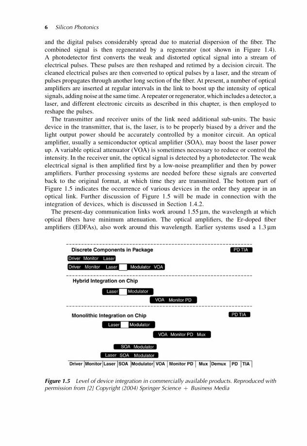
Figure 1.5 indicates the occurrence of various devices in the order they appear in an
optical link. Further discussion of Figure 1.5 will be made in connection with the
integration of devices, which is discussed in Section 1.4.2.
The present-day communication links work around 1.55mm, the wavelength at which
optical fibers have minimum attenuation. The optical amplifiers, the Er-doped fiber
amplifiers (EDFAs), also work around this wavelength. Earlier systems used a 1.3mm
Figure 1.5 Level of device integration in commercially available products. Reproduced withpermission from [2] Copyright (2004) Springer Science þ Business Media
6 Silicon Photonics

transmission window of the fiber, at which the material dispersion of the fiber is minimum.
The DWDM system employs hundreds of wavelengths, separated approximately from each
other by about 100GHz (0.8 nm), covering both the 1.3 and 1.55 mm windows.
The requirement that all the optoelectronic and electronic components must work at
the two wavelengths completely rules out the use of silicon-based active devices in the
telecommunicationsnetwork, since the cutoffwavelength ofSi is about1.1mm.Thematerials
of choice are quaternary alloy InGaAsP and ternary alloy InGaAs grown on InP substrate.
1.4.2 Materials and Integration
There are many differences between today’s microelectronics and photonics industries.
While silicon is the only material in the former, a variety of materials are used in photonics.
InP substrate is used for source and detector development, silica as the fiber material,
different semiconductors and even insulators like LiNbO3 formodulators, an Si platform for
passive lightwave circuits used in DWDM, and Si-based ICs for driver and controller
circuits. No single material or single technology is leading the market. The production
technology is still primitive, and the level of integration is far below the level achieved in
microelectronics.
In a truly monolithic IC, all components, that is, electronic circuits, light sources,
photodetectors, modulators, waveguides, multiplexers, and so on, are grown on the same
piece of semiconductor substrate. Since good sources and modulators have not yet been
realized using silicon, and since efficient silicon photodetectors do not exist at 1.55 mm,
monolithic integration on a silicon platform is at present ruled out. It is possible, in principle,
to use InP substrate for integration. However, the small wafer size, high cost, and other
factors limiting the manufacturability have hindered progress in this direction.
Hybrid integration, in which disparate parts are assembled onto one common platform,
has been pursued for quite some time. In common hybrid optical components, III–V
compound light sources and detectors are attached onto silicon on insulator (SOI), silica, or
polymer platforms. These components are commercially available. Figure 1.5 gives
examples of discrete components in package, hybrid integration, and monolithic integra-
tion. The order of the devices on the axis agrees with the order of appearance of the devices
in an optical link. As mentioned already, monolithic integration is almost exclusively on an
InP platform; however, photodetectors and transimpedance amplifiers (TIAs) have been
grown on silicon.
The main interest in hybrid technologies lies in the combination of III–V semiconductor
laser diodes with Si integrated circuits for optical fiber communication or optical inter-
connects. For this purpose, GaAs or InP is grown on Si and then processed, or, alternatively,
laser devices are detached from their substrate by an epitaxial liftoff process and then
bonded to Si substrate.
For growth of GaAs and InP on Si, the large lattice mismatch (4% for GaAs and 8% for
InP), different thermal expansion coefficients, and fast diffusion of Si as impurities all create
difficulties inmaintaining low defect densities in compounds for laser production. Although
several new techniques have been developed to overcome these difficulties, it is too early to
predict the long-term success of the techniques.
In the epitaxial liftoff technique, wet chemical etching is performed and then the III–V
heterostructure is floated off and transferred to a planar Si substrate. The bonding occurs due
Introduction to Silicon Photonics 7

to thevan derWaals force. In thewafer fusion process, the twomaterials (of high quality) are
brought into intimate contact under hydrogen ambient at around 450 �C. Under uniformdirect pressure, the substrates form robust chemical bonds. One of the substrates, for
example compound semiconductor, is selectively etched and photonic devices grown onto it
are integrated with silicon electronic circuits. Once again, it is difficult to predict how far
these technologies will be successful in commercial production.
It appears, therefore, that themost satisfactory solution to the above-mentioned problems
would be achievedwhen all the optoelectronic and photonic components could be grown on
a single substrate, for which silicon seems to be the best choice. The extensive experience in
Si fabrication and processing could then be put to maximum use. Unfortunately, however,
the lack of suitable emitter and especially a laser based on Si, as well as of a fast modulator,
stands in the way of achieving the coveted goal.
1.5 Data Network
While long-haul optical communication systems work at 1.55mm, to exploit the minimum
attenuation in the fiber, local area networks span smaller distance and area. In this case,
working at other wavelengths, at the cost of higher attenuation of signals, may be of
advantage due to the availability of cheap components. A possible system employs GaAs-
based lasers at around 800 nm, at which wavelength Si photodetectors and other electronic
circuits would offer a low-cost solution. If, in addition, Si emitters are available, further
reduction in cost is highly expected.
A large part of data communication network is anchored to servers and desktop
computers that utilize Si devices. The large potential volume of the market and the
competition with copper cables will necessitate more use of inexpensive optical fibers.
Si-based photonic components will offer the cheapest solution to the network.
1.6 Conclusions
From the discussions in the above sections, the following points emerge:
. The interconnect problemwithin a chip is taking an alarming shape. Optical interconnect
based on silicon technology may offer a viable solution.. The long-haul optical communication link employs at present a number of different
devices (viz., lasers, modulators, power monitor and control, amplifiers, photodetectors,
photoreceivers, multiplexers, demultiplexers, filters and other passive lightwave circuits,
and active network components like wavelength converters, etc.). Apart from passive
components, most of the active components are fabricated on the InP platform. A truly
monolithic OEIC on silicon may offer all the advantages of integration including cost
reduction.. Si-based photonic devices may offer lower cost in the sector of data networks covering
shorter distances.. Si microphotonics seem to be an attractive solution for next-generation optical inter-
connects for chip-to-chip or board-to-board interconnects.. Discrete silicon photonic devices like light-emitting diodes (LEDs) and lasers are in
demand for consumer electronics, display, and mobile communication, and as mid-
infrared or THz emitters.
8 Silicon Photonics