reconfigurable electro-optical waveguide for optical processing
TRANSCRIPT
Reconfigurable electro-optical waveguidefor optical processing
D. Dragoman and M. Dragoman
A highly versatile electro-optically induced waveguide is proposed, and some of its applications arediscussed. The In1�sGasAstP1�t-based device can reconfigure an arbitrary refractive-index profile withhigh speed by using an array of stripe electrodes deposited along the device. This device can act as avariable fractional Fourier transformer or as a beam shaper. Some nonguiding applications based on aspecific refractive-index patterning that is normal to the light-propagation direction, such as phasemodulation and beam steering, can also be implemented with this device. © 2003 Optical Society ofAmerica
OCIS codes: 230.0230, 230.7390, 070.0070, 070.4560.
1. Introduction
The spatial dependence of refractive index n�x, y� inany optical waveguide is prescribed in the fabricationprocess. As the waveguide modes and their propa-gation constants are determined by the refractive-index profile,1 tuning these parameters implies thepossibility of controlling and hence of changing n�x,y�. Such a reconfigurable waveguide has many ap-plications. For example, one can control both theshape of the output field and its spatial extent byexciting specific waveguide modes that can be ob-tained by specifically tailoring the refractive-indexprofile. Therefore a reconfigurable waveguide canact as a beam-matching device when n�x, y� ischanged such that the output field has an optimumspatial extent or an angular divergence to fit anotherwaveguide or detector. Alternatively, a change inn�x, y� can transform the irradiance pattern of thelight at the waveguide output into a desired form.Finally, variable integral transforms can be imple-mented with a waveguide that has a refractive-indexprofile that can be changed to a desired form. Otherapplications can be imagined as well.
D. Dragoman �[email protected]� is with the PhysicsFaculty, University of Bucharest, P.O. Box MG-11, 76900 Bucha-rest, Romania. M. Dragoman is with the National Institute forResearch and Development in Microtechnology, P.O. Box 38-160,72225 Bucharest, Romania.
Received 17 February 2003; revised manuscript received 5 Au-gust 2003.
0003-6935�03�326439-06$15.00�0© 2003 Optical Society of America
1
In this paper we present a reconfigurablewaveguide with a refractive-index profile that can betuned by use of the electro-optic effect. The electro-optic effect has been often employed as a means oftuning the refractive indices of waveguides for phaseor amplitude modulation applications, includingswitching.2 However, in almost all applications therefractive index was modified by the application of abias voltage onto a single electrode deposited over thewaveguide; the refractive index of the entirewaveguide was changed in one step. The only ex-ception to that modification method, to the authors’knowledge, is the device described in Ref. 3, in whichan array of individually addressable electrodes wasused for beam steering. Our device uses the electro-optical effect to implement a multistep change in therefractive index of a semiconductor slab to obtainprimarily waveguides with desired characteristics; inthis respect the reconfigurable waveguide is a newdevice. The applications of this waveguide, includ-ing its functioning as a one-chip optical tomographydevice that is able to implement a variable fractionalFourier transform �FRFT� and as a beam-shaping–matching device, are also presented. Other non-guiding applications, based on refractive-indexpatterning normal to the light-propagation direction,such as phase modulation and beam steering, canalso be implemented with the device presented in thispaper.
2. Design and Implementation of the ReconfigurableWaveguide
A material with the largest electro-optic effect is thecompound In Ga As P . The dependence of its
1�s s t 1�t0 November 2003 � Vol. 42, No. 32 � APPLIED OPTICS 6439

refractive index and its electro-optic coefficient r41 ons, t, and wavelength � are described in Ref. 4. Anelectric field E applied to the In1�sGasAstP1�t lattice-matched compound grown upon an InP substrate, forwhich s � 0.1894t��0.4184 � 0.013t�, produces arefractive-index change �n�t, �, E� � n0
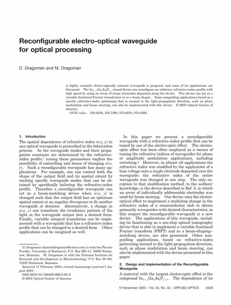
3�t, ��r41�t,��E, where n0�t, �� is the refractive index in the ab-sence of the electric field. For the wavelength ofinterest our first task is to choose t such that thematerial is transparent and its relative refractive-index change is maximum. Figure 1 represents thedependence of the scaled relative refractive-indexvariation ��t, �� � 1010n0
2�t, ��r41�t, �� on t for threewavelength values: 1.5 �m �solid curve�, 1.33 �m�dotted curve�, and 1 �m �dashed curve�. The rangeof variation for t for all three curves in Fig. 1 corre-sponds to the range for which the material is trans-parent, i.e., for which the refractive index is real; forlarger t values it becomes complex.
Therefore a device intended to work at a wave-length of 1.5 �m should be made from a compoundwith t � 0.84 �the value of s is related to that of t asdescribed above�. Our device works as a waveguideif the refractive index along the waveguide directionis constant but varies in the transversal directionsuch that the refractive index decreases from thecenter �core region� to the periphery �cladding re-gion�. A schematic representation of a device that
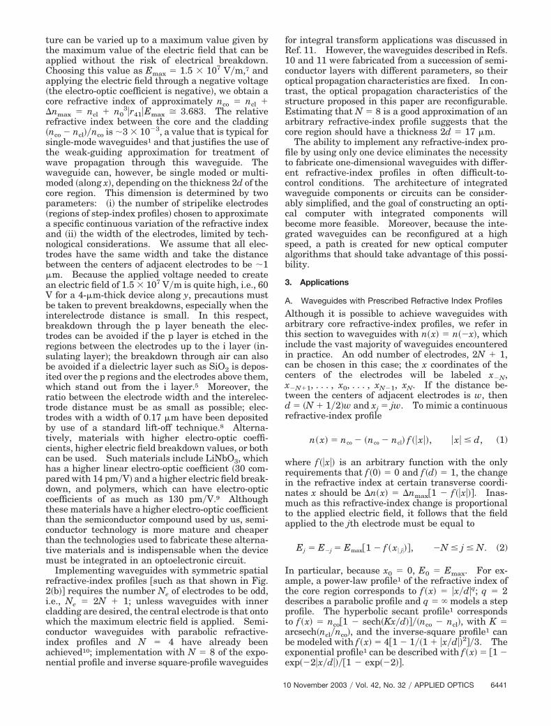
satisfies this requirement is shown in Fig. 2�a�. Thethick layer of In0.61Ga0.39As0.84P0.16, which is thelayer through which light propagates, cannot be indirect contact with the electrodes because the opticallosses in the metallic electrodes, as well as the leak-age currents at high electric fields, can be significant.To reduce the optical losses and leakage currents, oneshould apply the voltage through a reverse bias p–i–nInP�In0.61Ga0.39As0.84P0.16�InP structure. The topside of the structure is patterned by an array of par-allel metallic electrodes �contacts� that are needed tomodify independently the refractive indices of thestripes situated below the electrodes. The elec-trodes should be patterned on the doped InP layerssuch that the field propagating in theIn0.61Ga0.39As0.84P0.16 layer does not come into directcontact with the electrodes. Although, strictlyspeaking, the refractive index changes as a result ofthe electro-optic effects only beneath the electrodes,and retains its value in the spaces between the elec-trodes, in reality the electric field also penetrates asmall distance into the interelectrode spacing. Soappropriately choosing the interelectrode distancewill cause the refractive-index change to have a truesteplike profile. Interelectrode distances as small as1 nm have been reported.5 The dc bias necessary toinduce the electro-optical effect in the waveguide isapplied between the electrodes on the top side andthe back side of the structure, which is fully metal-lized. The bias on each electrode can be controlledindependently and can be changed electronically tothe desired value with switching speeds up to a fewgigahertz.6 Modifying the refractive-index bymeans of the electro-optic effect along the x directioncan induce a guiding action along the z direction; therefractive index does not depend on y.
The resultant waveguide is thus reconfigurableonly with respect to n�x� and can be used to processonly one-dimensional light beams. The noncon-tacted part of the material represents the waveguidecladding and has a refractive index ncl � n0 � 3.672.The refractive index of the contacted part of the struc-
Fig. 1. Dependence of scaled relative refractive-index variation��t, �� � 1010n0
2�t, ��r41�t, �� on t for three wavelengths: 1.5 �m�solid curve�, 1.33 �m �dotted curve�, and 1 �m �dashed curve�.
Fig. 2. �a� Schematic representation of the electro-optically induced waveguide. �b� Example of an induced refractive-index profile.
6440 APPLIED OPTICS � Vol. 42, No. 32 � 10 November 2003
ture can be varied up to a maximum value given bythe maximum value of the electric field that can beapplied without the risk of electrical breakdown.Choosing this value as Emax � 1.5 � 107 V�m,7 andapplying the electric field through a negative voltage�the electro-optic coefficient is negative�, we obtain acore refractive index of approximately nco � ncl �nmax � ncl n0
3�r41�Emax � 3.683. The relativerefractive index between the core and the cladding�nco � ncl��nco is 3 � 10�3, a value that is typical forsingle-mode waveguides1 and that justifies the use ofthe weak-guiding approximation for treatment ofwave propagation through this waveguide. Thewaveguide can, however, be single moded or multi-moded �along x�, depending on the thickness 2d of thecore region. This dimension is determined by twoparameters: �i� the number of stripelike electrodes�regions of step-index profiles� chosen to approximatea specific continuous variation of the refractive indexand �ii� the width of the electrodes, limited by tech-nological considerations. We assume that all elec-trodes have the same width and take the distancebetween the centers of adjacent electrodes to be 1�m. Because the applied voltage needed to createan electric field of 1.5 � 107 V�m is quite high, i.e., 60V for a 4-�m-thick device along y, precautions mustbe taken to prevent breakdowns, especially when theinterelectrode distance is small. In this respect,breakdown through the p layer beneath the elec-trodes can be avoided if the p layer is etched in theregions between the electrodes up to the i layer �in-sulating layer�; the breakdown through air can alsobe avoided if a dielectric layer such as SiO2 is depos-ited over the p regions and the electrodes above them,which stand out from the i layer.5 Moreover, theratio between the electrode width and the interelec-trode distance must be as small as possible; elec-trodes with a width of 0.17 �m have been depositedby use of a standard lift-off technique.8 Alterna-tively, materials with higher electro-optic coeffi-cients, higher electric field breakdown values, or bothcan be used. Such materials include LiNbO3, whichhas a higher linear electro-optic coefficient �30 com-pared with 14 pm�V� and a higher electric field break-down, and polymers, which can have electro-opticcoefficients of as much as 130 pm�V.9 Althoughthese materials have a higher electro-optic coefficientthan the semiconductor compound used by us, semi-conductor technology is more mature and cheaperthan the technologies used to fabricate these alterna-tive materials and is indispensable when the devicemust be integrated in an optoelectronic circuit.
Implementing waveguides with symmetric spatialrefractive-index profiles �such as that shown in Fig.2�b�� requires the number Ne of electrodes to be odd,i.e., Ne � 2N 1; unless waveguides with innercladding are desired, the central electrode is that ontowhich the maximum electric field is applied. Semi-conductor waveguides with parabolic refractive-index profiles and N � 4 have already beenachieved10; implementation with N � 8 of the expo-nential profile and inverse square-profile waveguides
for integral transform applications was discussed inRef. 11. However, the waveguides described in Refs.10 and 11 were fabricated from a succession of semi-conductor layers with different parameters, so theiroptical propagation characteristics are fixed. In con-trast, the optical propagation characteristics of thestructure proposed in this paper are reconfigurable.Estimating that N � 8 is a good approximation of anarbitrary refractive-index profile suggests that thecore region should have a thickness 2d � 17 �m.
The ability to implement any refractive-index pro-file by using only one device eliminates the necessityto fabricate one-dimensional waveguides with differ-ent refractive-index profiles in often difficult-to-control conditions. The architecture of integratedwaveguide components or circuits can be consider-ably simplified, and the goal of constructing an opti-cal computer with integrated components willbecome more feasible. Moreover, because the inte-grated waveguides can be reconfigured at a highspeed, a path is created for new optical computeralgorithms that should take advantage of this possi-bility.
3. Applications
A. Waveguides with Prescribed Refractive Index Profiles
Although it is possible to achieve waveguides witharbitrary core refractive-index profiles, we refer inthis section to waveguides with n�x� � n��x�, whichinclude the vast majority of waveguides encounteredin practice. An odd number of electrodes, 2N 1,can be chosen in this case; the x coordinates of thecenters of the electrodes will be labeled x�N,x�N1, . . . , x0, . . . , xN�1, xN. If the distance be-tween the centers of adjacent electrodes is w, thend � �N 1�2�w and xj � jw. To mimic a continuousrefractive-index profile
n� x� � nco � �nco � ncl� f ��x��, �x� � d, (1)
where f ��x�� is an arbitrary function with the onlyrequirements that f �0� � 0 and f �d� � 1, the changein the refractive index at certain transverse coordi-nates x should be �n�x� � �nmax�1 � f ��x���. Inas-much as this refractive-index change is proportionalto the applied electric field, it follows that the fieldapplied to the jth electrode must be equal to
Ej � E�j � Emax�1 � f � x� j���, �N � j � N. (2)
In particular, because x0 � 0, E0 � Emax. For ex-ample, a power-law profile1 of the refractive index ofthe core region corresponds to f �x� � �x�d�q; q � 2describes a parabolic profile and q � models a stepprofile. The hyperbolic secant profile1 correspondsto f �x� � nco�1 � sech�Kx�d����nco � ncl�, with K �arcsech�ncl�nco�, and the inverse-square profile1 canbe modeled with f �x� � 4�1 � 1��1 �x�d��2��3. Theexponential profile1 can be described with f �x� � �1 �exp��2�x�d����1 � exp��2��.
10 November 2003 � Vol. 42, No. 32 � APPLIED OPTICS 6441
B. Integrated Implementation of a Variable FractionalFourier Transform
The applications of the FRFT in optical signal pro-cessing and characterization are reviewed in Ref. 12.One of the most interesting is optical tomography,which is able to reconstruct a complex optical fieldfrom the square modulus of its FRFTs with variabledegrees of fractionality. Several devices have beenproposed for implementing FRFTs with variable de-grees of fractionality. They include fake zoom lens-es,13 which necessitate movable elements in thesetup; varifocal lenses, which are difficult to fabri-cate14; and pointlike white-light sources15 that hardlycorrespond to any real light source. Other setupsdisplay simultaneously, in a multichannel approach,different FRFT orders obtained through complicatedmultistrip masks,16 generate a FRFT with a contin-uously varying degree of fractionality for a givenvalue of its argument,17 or use several dynamicallyadjustable focal-length lenses in setups that consistof lenses and fixed free spaces.18 The approach toimplementing a FRFT with the variable degree offractionality that we propose is based on the fact thata graded-index �GRIN� waveguide with a parabolicrefractive-index profile n�x� � nco�1 � A2x2�2� andlength L transforms the input light distribution ��x�in its FRFT, F��u����, with a degree of fractionality� � AL.12 This FRFT is defined as
F��u���� �exp�i��4 � i��2�
�2� sin ��1�2 � �� x�
� exp� ikncoA2 sin �
��u2 � x2�cos � � 2ux�� ,
(3)
where k � 2��� is the wave number of light. � � 0�or � � 2�� corresponds to the identity operator, � ���2 to the usual Fourier transform, and � � � to theparity operator.
A change over the full range of variation of �, i.e.,a change in 2� with the degree of fractionality, im-plies a change in A with 2��L. Because in our caseA � �2�nmax��ncl �nmax��
1�2�d, one can achieve avariation in A easily by changing �nmax by means ofEmax. So to achieve a FRFT with a variable degreeof fractionality one must first, as discussed in Sub-section 3.A, obtain a GRIN waveguide with a para-bolic refractive-index profile. Then one should scalethe electric fields applied to all sections by Emax��Emax. The resultant waveguide will also have a par-abolic refractive-index profile, with A replaced by A�� �2�nmax���ncl �nmax���
1�2�d, where �nmax� is themaximum refractive-index change between core andcladding that one can achieve by applying maximumfield Emax�. To avoid the risk of an electrical break-down it is advisable to start first with Emax � 1.5 �107 V�m and then to decrease this electric field pro-gressively as it is applied to the central electrodeuntil Emax� � 0.84 � 107 V�m. A change of A with2��L corresponds thus to a change in the electric field
applied to the x0 electrode �on the central electrode�with 0.66 � 107 V�m for L � 2.8 mm and 2d � 17 �m.The waveguide length was chosen such that, forEmax � 1.5 � 107 V�m, AL is an even multiple of �.Each time the electric field on the central electrode ischanged, the electric fields on all other electrodesmust be scaled accordingly to preserve the parabolicprofile of the refractive index. A fully integrated de-vice can be made in this way for the specific task ofoptical tomography. This device has no movableparts, its degree of fractionality can be modified prac-tically continuously, and it can be integrated withother components such as semiconductor diode lasersand detectors in a one-chip optical tomograph.
3. Beam Shaping and Matching
In some applications it is sometimes important tohave an irradiance pattern of a certain form or to beable to transform the spatial extent or the angulardivergence of the incoming beam to couple it opti-mally to a further waveguide or detector. This canbe done with a waveguide with a certain refractive-index profile. Inasmuch as in a multimodewaveguide the normal modes, with different shapes,propagate independently with different propagationconstants, the shape, spatial extent, or angular di-vergence of the output beam depends not only on thecorresponding parameter of the input beam but alsoon the waveguide’s refractive-index profile and on itslength. For simplicity, we again discuss a parabolicGRIN waveguide of length L for which n�x� � nco�1 �A2x2�2�. The TE modes are, in this case,1 �m�x� �Hm�xV1�2�d�exp��x2V�2d2�, where V � kAncod
2 isthe normalized frequency of the waveguide and Hmare Hermite polynomials of order m. They propa-gate with propagation constants �m � knco � A�m 1�2�.
Let us consider now a steplike incident field with��x� � 1 for �x� � xmax and ��x� � 0 otherwise, whichexcites only the first M TE modes in the parabolicGRIN waveguide. Then the optical field at the out-put of the waveguide is given by
�out� x� � �m�0
M
am�m� x�exp�i�m L�, (4)
where am � � ��x��m�x�dx�� �m2�x�dx. If ��x� �
���x�, as in our example, only the even-order modesare excited. Because the propagation constants ofthe waveguide modes are different, the intensity dis-tribution of the output mode Iout � ��out�
2 depends onL for fixed A or on A for fixed L. So the shape of theincident beam can differ considerably from the shapeof the output beam. For example, Fig. 3 demon-strates the evolution of the output intensity for theparabolic GRIN waveguide discussed in Section 2 forwhich AL equals an even multiple of � when theelectric field on the central electrode equals Emax �1.5 � 107 V�m. Suppose that only the modes withm � 0, 2, 4, 6 are excited by an input steplike fieldwith xmax � 4��kAnco; the output intensity in nor-malized coordinates X � x�kAnco will be represented
6442 APPLIED OPTICS � Vol. 42, No. 32 � 10 November 2003
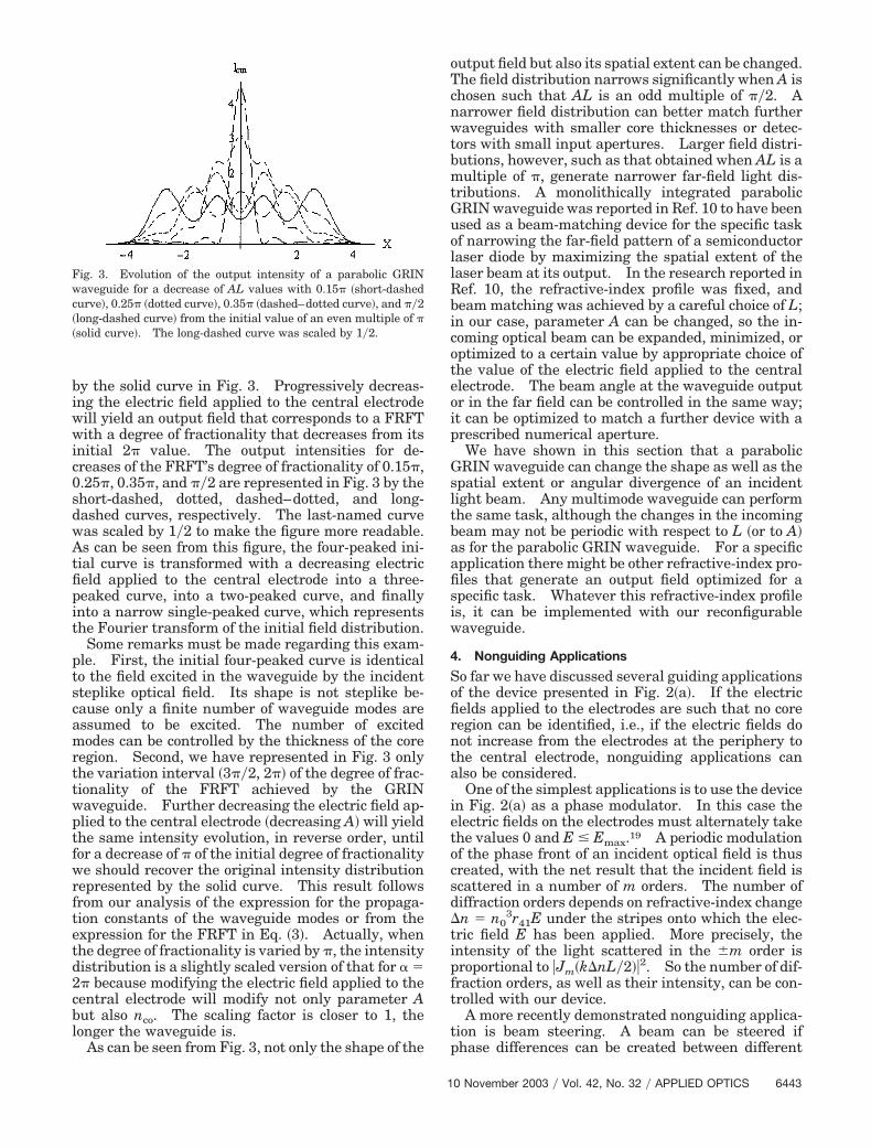
by the solid curve in Fig. 3. Progressively decreas-ing the electric field applied to the central electrodewill yield an output field that corresponds to a FRFTwith a degree of fractionality that decreases from itsinitial 2� value. The output intensities for de-creases of the FRFT’s degree of fractionality of 0.15�,0.25�, 0.35�, and ��2 are represented in Fig. 3 by theshort-dashed, dotted, dashed–dotted, and long-dashed curves, respectively. The last-named curvewas scaled by 1�2 to make the figure more readable.As can be seen from this figure, the four-peaked ini-tial curve is transformed with a decreasing electricfield applied to the central electrode into a three-peaked curve, into a two-peaked curve, and finallyinto a narrow single-peaked curve, which representsthe Fourier transform of the initial field distribution.
Some remarks must be made regarding this exam-ple. First, the initial four-peaked curve is identicalto the field excited in the waveguide by the incidentsteplike optical field. Its shape is not steplike be-cause only a finite number of waveguide modes areassumed to be excited. The number of excitedmodes can be controlled by the thickness of the coreregion. Second, we have represented in Fig. 3 onlythe variation interval �3��2, 2�� of the degree of frac-tionality of the FRFT achieved by the GRINwaveguide. Further decreasing the electric field ap-plied to the central electrode �decreasing A� will yieldthe same intensity evolution, in reverse order, untilfor a decrease of � of the initial degree of fractionalitywe should recover the original intensity distributionrepresented by the solid curve. This result followsfrom our analysis of the expression for the propaga-tion constants of the waveguide modes or from theexpression for the FRFT in Eq. �3�. Actually, whenthe degree of fractionality is varied by �, the intensitydistribution is a slightly scaled version of that for � �2� because modifying the electric field applied to thecentral electrode will modify not only parameter Abut also nco. The scaling factor is closer to 1, thelonger the waveguide is.
As can be seen from Fig. 3, not only the shape of the
output field but also its spatial extent can be changed.The field distribution narrows significantly when A ischosen such that AL is an odd multiple of ��2. Anarrower field distribution can better match furtherwaveguides with smaller core thicknesses or detec-tors with small input apertures. Larger field distri-butions, however, such as that obtained when AL is amultiple of �, generate narrower far-field light dis-tributions. A monolithically integrated parabolicGRIN waveguide was reported in Ref. 10 to have beenused as a beam-matching device for the specific taskof narrowing the far-field pattern of a semiconductorlaser diode by maximizing the spatial extent of thelaser beam at its output. In the research reported inRef. 10, the refractive-index profile was fixed, andbeam matching was achieved by a careful choice of L;in our case, parameter A can be changed, so the in-coming optical beam can be expanded, minimized, oroptimized to a certain value by appropriate choice ofthe value of the electric field applied to the centralelectrode. The beam angle at the waveguide outputor in the far field can be controlled in the same way;it can be optimized to match a further device with aprescribed numerical aperture.
We have shown in this section that a parabolicGRIN waveguide can change the shape as well as thespatial extent or angular divergence of an incidentlight beam. Any multimode waveguide can performthe same task, although the changes in the incomingbeam may not be periodic with respect to L �or to A�as for the parabolic GRIN waveguide. For a specificapplication there might be other refractive-index pro-files that generate an output field optimized for aspecific task. Whatever this refractive-index profileis, it can be implemented with our reconfigurablewaveguide.
4. Nonguiding Applications
So far we have discussed several guiding applicationsof the device presented in Fig. 2�a�. If the electricfields applied to the electrodes are such that no coreregion can be identified, i.e., if the electric fields donot increase from the electrodes at the periphery tothe central electrode, nonguiding applications canalso be considered.
One of the simplest applications is to use the devicein Fig. 2�a� as a phase modulator. In this case theelectric fields on the electrodes must alternately takethe values 0 and E � Emax.19 A periodic modulationof the phase front of an incident optical field is thuscreated, with the net result that the incident field isscattered in a number of m orders. The number ofdiffraction orders depends on refractive-index change�n � n0
3r41E under the stripes onto which the elec-tric field E has been applied. More precisely, theintensity of the light scattered in the �m order isproportional to �Jm�k�nL�2��2. So the number of dif-fraction orders, as well as their intensity, can be con-trolled with our device.
A more recently demonstrated nonguiding applica-tion is beam steering. A beam can be steered ifphase differences can be created between different
Fig. 3. Evolution of the output intensity of a parabolic GRINwaveguide for a decrease of AL values with 0.15� �short-dashedcurve�, 0.25� �dotted curve�, 0.35� �dashed–dotted curve�, and ��2�long-dashed curve� from the initial value of an even multiple of ��solid curve�. The long-dashed curve was scaled by 1�2.
10 November 2003 � Vol. 42, No. 32 � APPLIED OPTICS 6443
parts of the beam. The interference between theseparts of the beam is responsible for the steering.Beam steering has important applications in spatialbeam modulation and is especially useful in opticalinterconnections as a beam router. Approximately3° steering was demonstrated when a phase shift wasinduced on half of a vertical-cavity surface-emittinglaser surface,6 whereas continuous steering angles upto 2° were obtained by use of an array of individuallyaddressable stripes composed of quantum-well mod-ulators.3 One can tune the steering angle by vary-ing the pattern of electric fields applied to theelectrodes. The possibility of enlarging the steeringangle to 12° by decreasing the thickness of the stripeswas also discussed in Ref. 3. When those previousresults are taken into account, it follows that thedevice depicted in Fig. 2�a� can steer a light beam.The electric field applied to the electrodes has in thiscase a value equal to 0 for half of the electrodes andequal to E � Emax for the other half �as in Ref. 6� ora more complicated pattern as in Ref. 3.
5. Conclusions
We have shown that it is possible to implement areconfigurable waveguide by using the electro-opticeffect in the compound In1�sGasAstP1�t. Weachieved a one-dimensional spatial variation of therefractive index by applying a variable electric field toan array of electrode stripes deposited along thewaveguide. The shape of the refractive-index profileis determined by the profile of the electric fields ap-plied to the individually addressable electrodes.This profile can be reconfigured with speeds up to afew gigahertz.
The applications of the reconfigurable waveguideas a variable FRFT and as a beam-shaping–matchingdevice have been discussed; a GRIN waveguide witha parabolic refractive-index profile was used as anexample. Other nonguiding applications werebriefly mentioned.
The proposed device is a highly versatile electro-optically induced waveguide that can be used formany practical purposes. A single device can act asreconfigurable waveguide, can be integrated intosingle-chip optical tomography, can shape an inci-dent beam into a desired form, and can also be usedin nonguiding applications.
References1. A. W. Snyder and J. D. Love, Optical Waveguide Theory �Chap-
man & Hall, London, 1983�.2. D. Dragoman and M. Dragoman, Advanced Optoelectronic De-
vices �Springer-Verlag, Berlin, 1999�.3. B. Pezeshki, R. B. Apte, S. M. Lord, and J. S. Harris, Jr.,
“Quantum well modulators for optical beam steering applica-tions,” IEEE Photon. Technol. Lett. 3, 790–792 �1991�.
4. S. Adachi and K. Oe, “Linear electro-optic effects in zincblende-type semiconductors: key properties of InGaAsP relevant todevice design,” J. Appl. Phys. 56, 74–80 �1984�.
5. A. F. Morpurgo, C. M. Marcus, and D. B. Robinson, “Controlledfabrication of metallic electrodes with atomic separation,”Appl. Phys. Lett. 74, 2084–2086 �1999�.
6. L. Fan, M. C. Wu, H. C. Lee, and P. Grodzinski, “Dynamicbeam switching of vertical-cavity surface-emitting lasers withintegrated optical beam routers,” IEEE Photon. Technol. Lett.9, 505–507 �1997�.
7. E. P. Burr, J. B. Song, A. J. Seeds, and C. C. Button, “28 psrecovery time in an InGaAsP�InGaAsP multiple-quantum-well saturable absorber employing carrier sweepout,” J. Appl.Phys. 90, 3566–3569 �2002�.
8. Y. Takagaki, E. Wiebicke, and K. H. Ploog, “Fabrication ofGHz-range surface-acoustic-wave transducers on LiNbO3 us-ing imprint technology,” Nanotechnology 13, 15–17 �2001�.
9. L. R. Dalton, “Rational design of organic electro-optic materi-als,” J. Phys. Condens. Matter 15, R897–R934 �2003�.
10. S. El Yumin, K. Komori, and S. Arai, “GaInAsP�InP semicon-ductor vertical GRIN-lens for semiconductor optical devices,”IEEE Photon. Technol. Lett. 6, 601–603 �1994�.
11. D. Dragoman and M. Dragoman, “Band-engineered semicon-ductor optical waveguides for integral transform implementa-tion,” J. Appl. Phys. 85, 3409–3412 �1999�.
12. A. W. Lohmann, D. Mendlovic, and Z. Zalevsky, “Fractionaltransformations in optics,” Prog. Opt. 38, 263–342 �1998�.
13. A. W. Lohmann, “A fake zoom lens for fractional Fourier ex-periments,” Opt. Commun. 115, 437–443 �1995�.
14. Y. Zhang, B.-Y. Gu, B.-Z. Dong, and G.-Z. Yang, “New opticalconfigurations for implementing Radon–Wigner display: ma-trix analysis approach,” Opt. Commun. 160, 292–300 �1999�.
15. Y. Zhang, B.-Y. Gu, B.-Z. Dong, and G.-Z. Yang, “Novel imple-mentation of the Radon–Wigner display,” Opt. Commun. 166,21–24 �1999�.
16. D. Mendlovic, R. G. Dorsch, A. W. Lohmann, Z. Zalevsky, andC. Ferreira, “Optical illustration of a varied fractional Fourier-transform order and the Radon–Wigner display,” Appl. Opt.35, 3925–3929 �1996�.
17. D. Dragoman, M. Dragoman, and K.-H. Brenner, “Experimen-tal demonstration of a continuously variant fractional Fouriertransformer,” Appl. Opt. 38, 4985–4989 �1999�.
18. M. Fatih Erden, H. M. Ozaktas, A. Sahin, and D. Mendlovic,“Design of dynamically adjustable anamorphic fractional Fou-rier transformer,” Opt. Commun. 136, 52–60 �1997�.
19. G. I. Stegeman and D. G. Hall, “Modulated index structures,”J. Opt. Soc. Am. A 7, 1387–1398 �1990�.
6444 APPLIED OPTICS � Vol. 42, No. 32 � 10 November 2003