real-time digital simulator with digital/analog conversion interface for testing power instruments
TRANSCRIPT
862 IEEE Transactions on Power Systems, Vol. 9, No. 2, May 1994
Real-Time Digital Simulator with Digital/Analog Conversion Interface for Testing Power Instruments
Hisao Taoka Isao Iyoda Hideo Noguchi
Mitsubishi Electric Corporation 8-1-1, Tsukaguchi-Honmachi
Amagasaki, Hyogo 661 Japan
Member, IEEE Member, IEEE
Abstract - The need for real-time simulation stems from the fact that in many practical situations it is desirable to analyze the dynamic behavior of a large power system with advanced equipment that has complex and high-speed performance. Analog simulators are effective, however they impose serious limitations on the size of the system that is being modeled. We have studied and developed a real- time digital simulator using a hypercube computer, and realized a real- time performance available for the analysis of large power systems.
Now as the second step of our study, we developed a digital/analog conversion interface for testing actual power instruments. The interface exchanges the variables of fundamental frequency domain in the real-time digital simulator, and the variables of exact time domain in the analog equipments connected to the simulator.
In this paper, we describe the detail of our developed digital/analog conversion interface of real-time digital simulator for testing advanced power instruments. Its conversion algorithm, system configuration of the simulator with the interface, experimental results are also presented in it.
Keyword - Power System Analysis, Simulation, Transient Stability, Long Term Dynamics, Numerical Analysis, Hypercube Computer, Real-Time Simulator, Parallel Processing, Analog-Digital Converter
INTRODUCTION
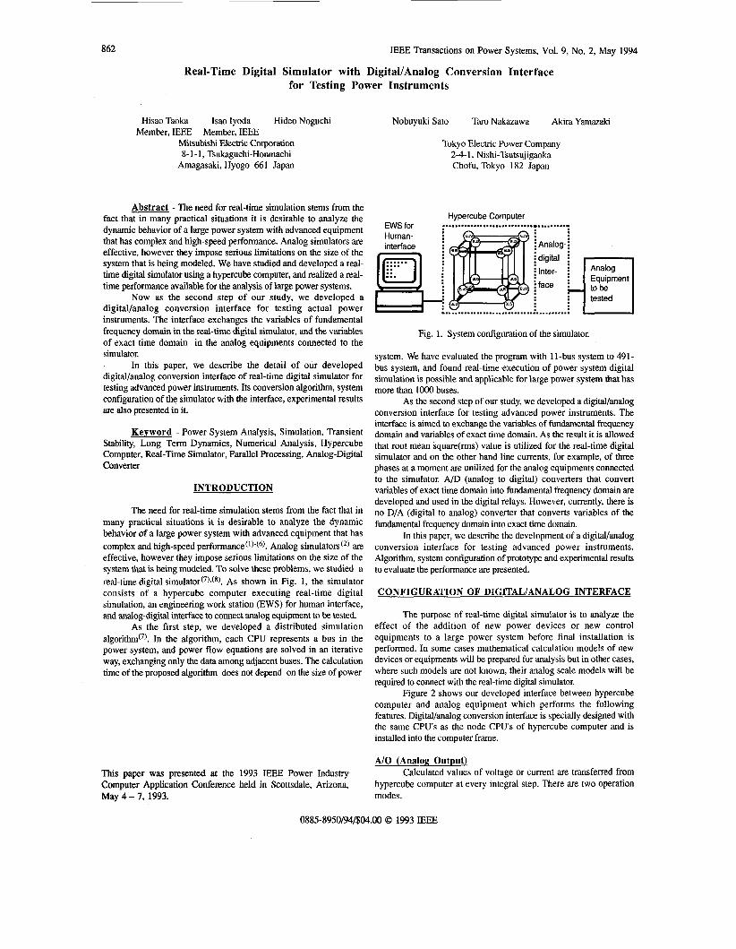
The need for real-time simulation stems from the fact that in many practical situations it is desirable to analyze the dynamic behavior of a large power system with advanced equipment that has complex and high-speed Analog simulators(2) are effective, however they impose serious limitations on the size of the system that is being modeled. To solve these problems, we studied a real-time digital As shown in Fig. 1 , the simulator consists of a hypercube computer executing real-time digital simulation, an engineering work station (EWS) for human interface, and analog-digital interface to connect analog equipment to be tested.
As the first step, we developed a distributed simulation In the algorithm, each CPU represents a bus in the
power system, and power flow equations are solved in an iterative way, exchanging only the data among adjacent buses. The calculation time of the proposed algorithm does not depend on the size of power
This paper was presented at the 1993 IEEE Power Industry Computer Application Conference held in Scottsdale, Arizona, May 4 - 7, 1993.
Nobuyuki Sat0 Taro Nakazawa Akira Yamazaki
Tokyo Electric Power Company 2-4-1, Nishi-Tsutsujigaoka Chofu, Tokyo 182 Japan
EWS for Human- interface
Hypercube Computer a............................ .......... -
! Analog- I :digital i i inter- I iface i - I .......... ,
Analog Equipment
tested I
Fig. 1. System configuration of the simulator.
system. We have evaluated the program with 1 I-bus system to 491- bus system, and found real-time execution of power system digital simulation is possible and applicable for large power system that has more than 1000 buses.
As the second step of our study, we developed a digital/analog conversion interface for testing advanced power instruments. The interface is aimed to exchange the variables of fundamental frequency domain and variables of exact time domain. As the result it is allowed that root mean square(rms) value is utilized for the real-time digital simulator and on the other hand line currents, for example, of three phases at a moment are unilized for the analog equipments connected to the simulator. A/D (analog to digital) converters that convert variables of exact time domain into fundamental frequency domain are developed and used in the digital relays. However, currently, there is no D/A (digital to analog) converter that converts variables of the fundamental frequency domain into exact time domain.
In this paper, we describe the development of a digital/analog conversion interface for testing advanced power instruments. Algorithm, system configuration of prototype and experimental results to evaluate the performance are presented.
CONFIGURATION OF DIGITAL/ANALOG INTERFACE
The purpose of real-time digital simulator is to analyze the effect of the addition of new power devices or new control equipments to a large power system before final installation is performed. In some cases mathematical calculation models of new devices or equipments will be prepared for analysis but in other cases, where such models are not known, their analog scale models will be required to connect with the real-time digital simulator.
Figure 2 shows our developed interface between hypercube computer and analog equipment which performs the following features. Digitalhalog conversion interface is specially designed with the same CPU's as the node CPU's of hypercube computer and is installed into the computer frame.
A/O (Analog Output) Calculated values of voltage or current are transferred from
hypercube computer at every integral step. There are two operation modes.
0885-8950/94/$04.00 0 1993 IEEE
863
1,o
1,o
HYPERCUBE COMPUTER SIMULATION DEDICATED D/A
NODES INTERFACE NODE +
+D + '- DIO 1. I .(-
1 VrmsorVdc (Irms or Idc)
-
(a) System Interface on signal level.
HYPERCUBE COMPUTER SIMULATION DEDICATED D/A POWER CURRENT
NODES INTERFACE NGDES AMPLIFIER SENSOR Vrms * N O t - p j + en-
c- lrms
Vrms
SIMULATION DEDICATED D/A POWER CURRENT NODES INTERFACE NGDES AMPLIFIER SENSOR
Vrms * N O t - p j + en-
c- lrms
ANALOG DEVICES V (1)
V (1)
ON, OFF
ON, OFF
ANALOG DEVICES
V I
+ ON, OFF 1,o
1,o ON, OFF
: SIGNAL FLOW AND ITS DIRECTIONS
(.) : POWER FLOW AND ITS DIRECTIONS
(b) System interface on power level. Fig. 2. Digital and analog interface.
(1) Three phase alternative current output mode The data is converted from digital root mean square value to
three-phase instantaneous analog value in real time. (a) Interface on signal level
The instantaneous value is connected directly to analog control equipment (e.g., actual protective relay equipment, prototype of advanced control equipment).
(b) Interface on power level The instantaneous value is connected to the analog equipment
through power amplifier to analog power device (e.g., models of generator, load). (2) Direct outputmode
analog value in real time in this mode. The data is converted from digital value to instantaneous
(a) Interface on signal level The instantaneous value is connected directly to analog control
equipment and models of multi variable control system, for example. (b) Interface of power level
The instantaneous value is connected through power amplifier to analog power devices referred to models of SMES, for example.
A/I (Analog Input) Instantaneous analog values of voltage or current are
converted to digital value and transferred to hypercube computer at every integral step. There are two operation modes.
( 1 )
square value.
Three-phase alternative current input mode Instantaneous analog values are converted to digital root mean
(2) Direct current input mode
values with sign flags. Instantaneous analog values are converted to digital average
DIO (Digital Output) ON/OFF signals for the purpose of output of control
command, of status monitoring, etc., are transferred from hypercube computer to analog equipment.
D/I (Digital Input1 ON/OFF signals for the purpose of input of control command,
of status monitoring, etc., are transferred from analog equipment to hypercube computer.
The followings are the main requirements and estimation items for all the parts of digital/analog conversion interface:
(1) Adequate accuracy shall be obtained. The accuracy, which will depend on both the resolution of D/A (digital to analog) converter or A/D (analog to digital) converter and the selected algorithm, will be estimated. (2) Time delay of conversion shall be minimized. Time delay, which will be caused by the interval of integral step and the selected algorithm, will be estimated. ( 3 ) Output of phase and/or amplitude of instantaneous value shall be gradually changed even when there is a sudden change of root mean square data (for three-phase alternative current output). As the simulation is executed in the domain of root mean square value, it is considered that the data are continuous during the interval of integral step. Therefore smoothing algorithm will be utilized. (4) Three-phase unbalance component and direct current component shall be eliminated (for three-phase alternative current output). As the unbalance component and direct current component are not essential for root mean square value calculation, the elimination algorithm will be utilized. (5) Adequate synchronization between AI0 and AII shall be considered (for power transfer). (6) Adequate feed back algorithms shall be considered along with A/O through A/I route (for power transfer).
ALGORITHMS FOR CONVERSION
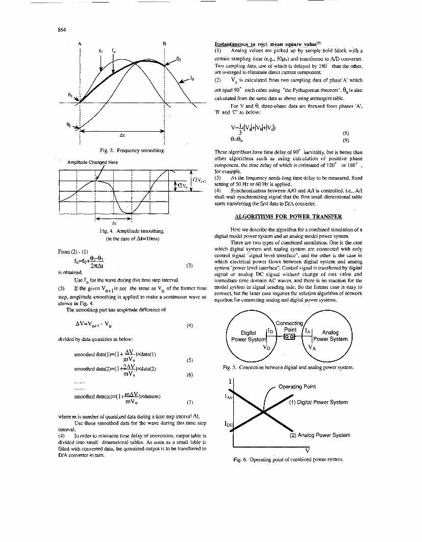
Root mean square to instantaneous value (1) V, 8 and f are given at each end of the integral step. Calculate sinusoidal waves (for three phase) and store the quantized values of the waves of one cycle into the output table. (2) If the given 8 is not the continuous value from the former time step, frequency smoothing is applied to make a continuous simusoidal wave as shown in Fig. 3.
At time "A", suppose the former wave phase angle is e,, and given wave phase angle and frequency are 8, and fo respectively. After a time step interval At, i.e., at time "B", phase angle 8, is assumed from the above 8, and f,.
The smoothing frequency fn from 8, to 8, will be calculated as follows:
Angle difference from time A to B under fo is
Angle difference from time A to B under f, is
03-01=2~fnAt
864
A fo f"
B
Fig. 3. Frequency smoothing.
Amplitude Changed Here /
:-: At
Fig, 4. Amplitude smoothing. (in the case of At=lOms)
From (2) - (1) f,=fo+82-B1
27cAt (3) is obtained.
Use f, for the wave during this time step interval. (3) If the given Vn+lis not the same as Vn of the former time step, amplitude smoothing is applied to make a continuous wave as shown in Fig. 4.
The smoothing part has amplitude difference of
AV=V,,, - V, (4)
divided by data quantities as below:
smoothed da ta( l )=( l+K)Xdata( l ) mVn (5)
smoothed data(2)=(1 + m ) X d a t a ( 2 ) mVn
......
...... smoothed data(m)=( l + u ) X d a t a ( m )
mVn (7)
where m is number of quantized data during a time step interval At. Use these smoothed data for the wave during this time step
interval. (4) In order to minimize time delay of conversion, output table is divided into small dimensional tables. As soon as a small table is filled with converted data, the quantized output is to be transferred to D/A converter in turn.
Instantaneous to root mean square value(g) ( 1 ) Analog values are picked up by sample hold block with a certain sampling time (e.g., 50p) and transferred to A/D converter. Two sampling data, one of which is delayed by 180" than the other, are averaged to eliminate direct current component. (2) v, is calculated from two sampling data of phase'A' which
are apart 90" each other using "the Pythagorean theorem". 8, is also calculated from the same data as above using arctangent table.
For V and 8, three-phase data are focused from phases 'A', 'B' and 'C' as below:
These algorithms have time delay of 90° inevitably, but is better than other algorithms such as using calculation of positive phase component, the time delay of which is estimated of 120" or 180° , for example. (3) As the frequency needs long time delay to be measured, fixed setting of 50 Hz or 60 Hz is applied. (4) Synchronization between A/O and AA is controlled, i.e., AA shall wait synchronizing signal that the first small dimensional table starts transferring the first data to D/A converter.
ALGORITHMS FOR POWER TRANSFER
Here we describe the algorithm for a combined simulation of a digital model power system and an analog model power system.
There are two types of combined simulation. One is the case which digital system and analog system are connected with only control signal "signal level interface", and the other is the case in which electrical power flows between digital system and analog system "power level interface". Control signal is transferred by digital signal or analog DC signal without change of rms value and immediate time domain AC waves, and there is no reaction for the model system in signal sending side. So the former case is easy to connect, but the latter case requires the solution algorithm of network equation for connecting analog and digital power systems.
Fig. 5. Connection between digital and analog power system.
I \
IAO (1) Digital Power System
ID0 I
(2) Analog Power System
Fig. 6. Operating point of combined power system.
865
0.9JUl - 0.9CrrcI
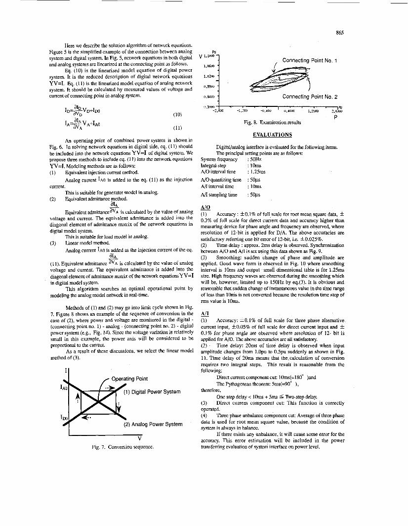
Here we describe the solution algorithm of network equations. Figure 5 is the simplified example of the connection between analog system and digital system. In Fig. 5, network equations in both digital and analog systems are linearized at the connecting point as follows.
Eq. (10) is the linearized model equation of digital power system. It is the reduced description of digital network equations Yv=I. Eq. (1 1) is the linearized model equation of analog network system. It should be calculated by measured values of voltage and current of connecting point in analog system. Connecting Point No. 2
(10)
An operating point of combined power system is shown in Fig. 6. In solving network equations in digital side, eq. (1 1) should be included into the network equations Yv=I of digital system. We propose three methods to include eq. (1 1) into the network equations Yv=I. Modeling methods are as follows: ( 1 ) Equivalent injection current method.
current.
(2) Equivalent admittance method.
Analog current IAO is added to the eq. (1 1) as the injection
This is suitable for generator model in analog.
- aIA Equivalent admittanceaVA is calculated by the value of analog
voltage and current. The equivalent admittance is added into the diagonal element of admittance matrix of the network equations in digital model system.
(3) Linear model method. "his is suitable for load model in analog.
Analog current 1.40 is added as the injection current of the eq.
(1 1). Equivalent admittance avA is calculated by the value of analog voltage and current. The equivalent admittance is added into the diagonal element of admittance matrix of the network equationsYV=I in digital model system.
This algorithm searches an optimal operational point by modeling the analog model network in real-time.
- 31,
Methods of (1) and (2) may go into limit cycle shown in Fig. 7. Figure 8 shows an example of the sequence of conversion in the case of (2), where power and voltage are monitored in the digital - (connecting point no. 1) - analog - (connecting point no. 2) - digital power system (e.g., Fig. 14). Since the voltage variation is relatively small in this example, the power axis will be considered to be proportional to the current.
As a result of these discussions, we select the linear model method of (3).
II
V Fig. 7. Conversion sequence.
v l.q , Connecting Point No. 1
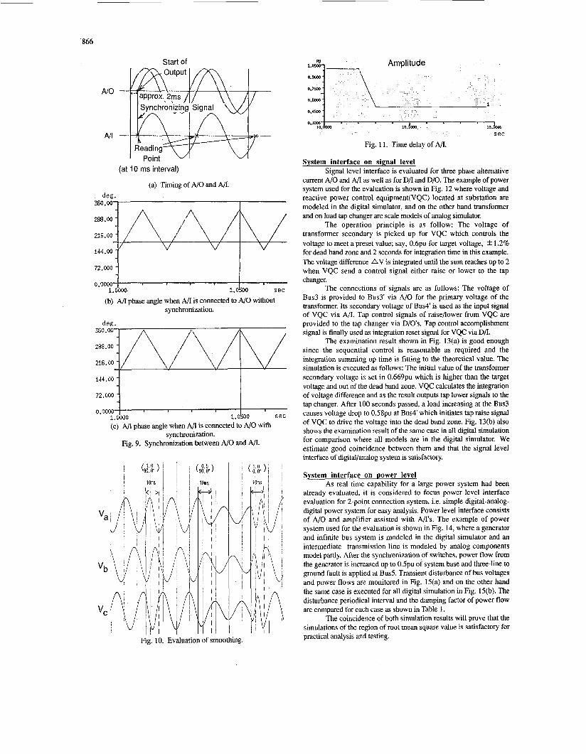
- A I 0 (1) Accuracy : * 0.1 % of full scale for root mean square data, f 0.3% of full scale for direct current data and accuracy higher than measuring device for phase angle and frequency are observed, where resolution of 12-bit is applied for D/A. The above accuracies are satisfactory referring one bit error of 12-bit, i.e. *0.025%. (2) Time delay : approx. 2ms delay is observed. Synchronization between AI0 and A/I is set using this data shown as Fig. 9. (3) Smoothing: sudden change of phase and amplitude are applied. Good wave form is observed in Fig. 10 where smoothing interval is lOms and output small dimensional table is for 1.25ms size. High frequency waves are observed during the smoothing which will be, however, limited up to 150Hz by eq.(3). It is obvious and reasonable that sudden change of instantaneous value in the time range of less than lOms is not converted because the resolution time step of rms value is 1 Oms.
AI1 (1) Accuracy: *0.1% of full scale for three phase alternative current input, +0.05% of full scale for direct current input and k 0.1% for phase angle are observed where resolution of 12- bit is applied for A/D. The above accuracies are all satisfactory. (2) Time delay: 20ms of time delay is observed when input amplitude changes from l.0pu to 0.5pu suddenly as shown in Fig. 11. Time delay of 20ms means that the calculation of conversion requires two integral steps. This result is reasonable from the following:
-
Direct current component cut: 10ms(=180° )and The Pythagorean theorem: 5ms(=90" ) ,
therefore, One step delay < lOms + 5ms 5 Two-step delay.
(3) Direct current component cut: This function is correctly operated. (4) Three phase unbalance component cut: Average of three phase data is used for root mean square value, because the condition of system is always in balance.
If there exists any unbalance, it will cause some error for the accuracy. This error estimation will be included in the power transfemng evaluation of system interface on power level.
X66
Start of
72.000 - 0 .oooo
NO
NI
(at 10 ms interval)
(a) Timing of N O and M. deg.
360.00 1 I
144 .OO 72.0001 , , , , I , s e c
0.0000 I. 0000 1.0 00
(c) A/I phase angle when A/r is connected to A/O with synchronization.
Fig. 9. Synchronization between A/O and M.
Fig. 10. Evaluation of smoothing.
0.3oOo' . . * . l 0 . b l*.iooO 1 O . h
sec Fig. 1 1. Time delay of AD.
System interface on signal level Signal level interface is evaluated for three phase alternative
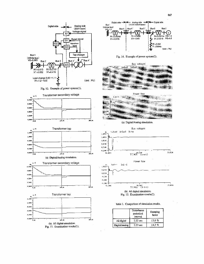
current A/O and M as well as for D/I and D/O. The example of power system used for the evaluation is shown in Fig. 12 where voltage and reactive power control equipment(VQC) located at substation are modeled in the digital simulator, and on the other hand transformer and on load tap changer are scale models of analog simulator.
The operation principle is as follow: The voltage of transformer secondary is picked up for VQC which controls the voltage to meet a preset value; say, 0.6pu for target voltage, k 1.2% for dead band zone and 2 seconds for integration time in this example. The voltage difference A V is integrated until the sum reaches up to 2 when VQC send a control signal either raise or lower to the tap changer.
The connections of signals are as follows: The voltage of Bus3 is provided to Bus3' via A/O for the primary voltage of the transformer. Its secondary voltage of Bus4 is used as the input signal of VQC via AD. Tap control signals of raise/lower from VQC are provided to the tap changer via D/Os. Tap control accomplishment signal is finally used as integration reset signal for VQC via DD.
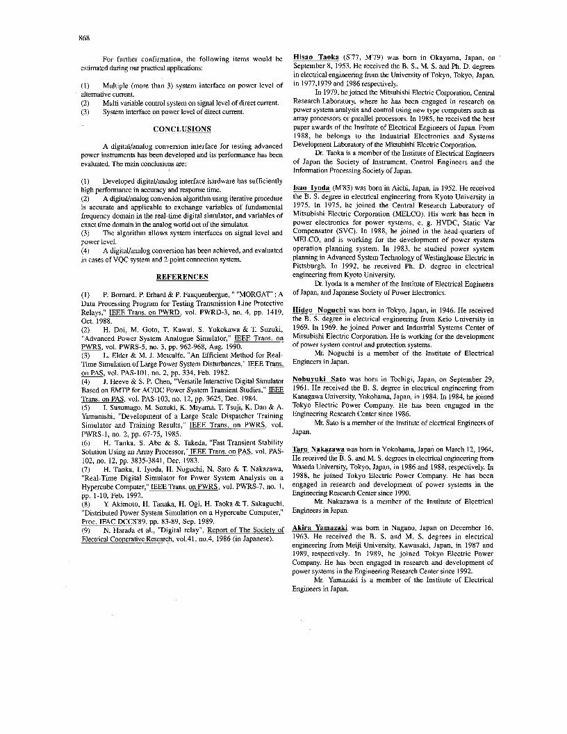
The examination result shown in Fig. 13(a) is good enough since the sequential control is reasonable as required and the integration summing up time is fitting to the theoretical value. The simulation is executed as follows: The initial value of the transformer secondary voltage is set in 0 . 6 6 9 ~ ~ which is higher than the target voltage and out of the dead band zone. VQC calculates the integration of voltage difference and as the result outputs tap lower signals to the tap changer. After 100 seconds passed, a load increasing at the Bus3 causes voltage drop to 0 . 5 8 ~ ~ at Bus4 which initiates tap raise signal of VQC to drive the voltage into the dead band zone. Fig. 13(b) also shows the examination result of the same case in all digital simulation for comparison where all models are in the digital simulator. We estimate good coincidence between them and that the signal level interface of digiWanalog system is satisfactory.
System interface on power level As real time capability for a large power system had been
already evaluated, it is considered to focus power level interface evaluation for 2-point connection system, i.e. simple digital-analog- digital power system for easy analysis. Power level interface consists of A/O and amplifier assisted with AD'S. The example of power system used for the evaluation is shown in Fig. 14, where a generator and infinite bus system is modeled in the digital simulator and an intermediate transmission line is modeled by analog components model partly. After the synchronization of switches, power flow from the generator is increased up to 0.5pu of system base and three-line to ground fault is applied at BusS. Transient disturbance of bus voltages and power flows are monitored in Fig. 15(a) and on the other hand the same case is executed for all digital simulation in Fig. 15(b). The disturbance periodical interval and the damping factor of power flow are compared for each case as shown in Table 1.
The coincidence of both simulation results will prove that the simulations of the region of root mean square value is satisfactory for practical analysis and testing.
867
~
Disturbance Damping periodical factor
interval All digital 2.22 sec 13.8 %
Digital side Analog side : (200V base) ' Voltage signal
I I
Digital/analog 2.23 sec
Bus 1 (Infinite bus)
14.3 %
XT=0.052 X1=0.416 i (Unit : PU) Load change 0.63-1.1 1
(R =1.2+0.9)
- Fig. 12. Example of power system(1).
.I Transformer secondary voltage
0.580
1: 4 Transformer tap
~~J 0.800)
0.7W
0.m .eo 1 .m .m
(a) Digital/Analog simulation.
1: 4 Transformer secondary voltage
0 . m c
1: 5 Transformer tap
(b) All digital simulation. Fig. 13. Examination results(1).
Digital side Analog side Digital side Bus 1 : (12.5V,40mA base) :
(Infinite bus)
Rf =0.002
(Unit : PU)
Fig. 14. Example of power system(2).
Bus voltaaes ,1B"s2 . - -- - --
~ = B U S ~ ~ = B U S ~
Power flow
(a) DigitaJ/Analog simulation.
Bus voltages pu 1=Bus2 2=Bus5 3-n.a.
1.1000
EII 0.7000
0.6000 50.0000 70.0000
Power flow PU 1=4-1 2=2-5
1.0000
0.6000
-0.600
-1.000 i 70.0000
:;::::p,-----, 50.0000 60.0000
TIME ( s e c )
(b) All digital simulation. Fig. 15. Examination results(2).
Table 1. Comparison of simulation results.
868
For further confirmation, the following items would be estimated during our practical applications:
(1) alternative current. (2) (3)
Multiple (more than 3) system interface on power level of
Multi variable control system on signal level of direct current. System interface on power level of direct current.
CONCLUSIONS
A digital/analog conversion interface for testing advanced power instruments has been developed and its performance has been evaluated. The main conclusions are:
(1) Developed digital/analog interface hardware has sufficiently high performance in accuracy and response time. (2) A digital/analog conversion algorithm using iterative procedure is accurate and applicable to exchange variables of fundamental frequency domain in the real-time digital simulator, and variables of exact time domain in the analog world out of the simulator. (3) The algorithm allows system interfaces on signal level and power level. (4) A digital/analog conversion has been achieved, and evaluated in cases of VQC system and 2-point connection system.
REFERENCES
(1) P. Bornard, P. Erhard & P. Fauquenbergue, " "MORGAT' : A Data Processing Program for Testing Transmission Line Protective Relays," IEEE Trans. on PWRD, vol. PWRD-3, no. 4, pp. 1419, Oct. 1988. (2) H. Doi, M. Goto, T. Kawai, S. Yokokawa & T. Suzuki, "Advanced Power System Analogue Simulator," IEEE Trans. on PWRS, vol. PWRS-5, no. 3, pp. 962-968, Aug. 1990. (3) L. Elder & M. J. Metcalfe, "An Efficient Method for Real- Time Simulation of Large Power System Disturbances," IEEE Trans. on PAS, vol. PAS-101, no. 2, pp. 334, Feb. 1982. (4) J. Heeve & S. P. Chen, "Versatile Interactive Digital Simulator Based on EMTP for AC/DC Power System Transient Studies," Trans. on PAS, vol. PAS-103, no. 12, pp. 3625, Dec. 1984. (5) I. Susumago, M. Suzuki, K. Miyama, T. Tsuji, K. Dan & A. Yamanishi, "Development of a Large Scale Dispatcher Training Simulator and Training Results," IEEE Trans. on PWRS, vol. PWRS-1, no. 2, pp. 67-75, 1985. (6) H. Taoka, S. Abe & S. Takeda, "Fast Transient Stability Solution Using an Array Processor," IEEE Trans. on PAS, vol. PAS- 102, no. 12, pp. 323353841, Dec. 1983. (7) H. Taoka, I. Iyoda, H. Noguchi, N. Sat0 & T. Nakazawa, "Real-Time Digital Simulator for Power System Analysis on a Hypercube Computer," IEEE Trans. on PWRS , vol. PWRS-7, no. 1, pp. 1-10, Feb. 1992. (8) Y Akimoto, H. Tanaka, H. Ogi, H. Taoka & T. Sakaguchi, "Distributed Power System Simulation on a Hypercube Computer," Proc. IFAC DCCS'89, pp. 83-89, Sep. 1989. (9) N. Harada et al., "Digital relay", Report of The Society of Electrical Cooperative Research, vo1.41, 110.4, 1986 (in Japanese).
Hisao Taoka (S'77, M'79) was born in Okayama, Japan, on September 8, 1953. He received the B. S., M. S. and Ph. D. degrees in electrical engineering from the University of Tokyo, Tokyo, Japan. in 1977,1979 and 1986 respectively.
In 1979, he joined the Mitsubishi Electric Corporation, Central Research Laboratory, where he has been engaged in research on power system analysis and control using new type computers such as array processors or parallel processors. In 1985, he received the best paper awards of the Institute of Electrical Engineers of Japan. From 1988, he belongs to the Industrial Electronics and Systems Development Laboratory of the Mitsubishi Electric Corporation.
Dr. Taoka is a member of the Institute of Electrical Engineers of Japan the Society of Instrument, Control Engineers and the Information Processing Society of Japan.
Isao Iyoda (M'83) was born in Aichi, Japan, in 1952. He received the B. S. degree in electrical engineering from Kyoto University in 1975. In 1975, he joined the Central Research Laboratory of Mitsubishi Electric Corporation (MELCO). His work has been in power electronics for power systems, e. g. HVDC, Static Var Compensator (SVC). In 1988, he joined in the head-quarters of MELCO, and is working for the development of power system operation planning system. In 1983, he studied power system planning in Advanced System Technology of Westinghouse Electric in Pittsburgh. In 1992, he received Ph. D. degree in electrical engineering from Kyoto University.
Dr. Iyoda is a member of the Institute of Electrical Engineers of Japan, and Japanese Society of Power Electronics.
Hideo Noguchi was born in Tokyo, Japan, in 1946. He received the B. S. degree in electrical engineering from Keio University in 1969. In 1969, he joined Power and Industrial Systems Center of Mitsubishi Electric Corporation. He is working for the development of power system control and protection systems.
Mr. Noguchi is a member of the Institute of Electrical Engineers in Japan.
Nobuyuki Sat0 was born in Tochigi, Japan, on September 29, 1961. He received the B. S. degree in electrical engineering from Kanagawa University, Yokohama, Japan, in 1984. In 1984, he joined Tokyo Electric Power Company. He has been engaged in the Engineering Research Center since 1986.
Mr. Sat0 is a member of the Institute of electrical Engineers of Japan.
Taro Nakazawa was born in Yokohama, Japan on March 12, 1964. He received the B. S. and M. S. degrees in electrical engineering from Waseda University, Tokyo, Japan, in 1986 and 1988, respectively. In 1988, he joined Tokyo Electric Power Company. He has been engaged in research and development of power systems in the Engineering Research Center since 1990.
Mr. Nakazawa is a member of the Institute of Electrical Engineers in Japan.
Akira Yamazaki was born in Nagano, Japan on December 16, 1963. He received the B. S. and M. S. degrees in electrical engineering from Meiji University, Kawasaki, Japan, in 1987 and 1989, respectively. In 1989, he joined Tokyo Electric Power Company. He has been engaged in research and development of power systems in the Engineering Research Center since 1992.
Mr. Yamazaki is a member of the Institute of Electrical Engineers in Japan.