review article: rare-earth monosulfides as …pboolcha/papers/2011/review article rare...review...
TRANSCRIPT
Review Article: Rare-earth monosulfides as durable and efficient cold cathodesa)
Marc Cahayb) and Punit BoolchandSchool of Electronic and Computing Systems, University of Cincinnati, Cincinnati, Ohio 45221
Steven B. Fairchild and Larry GrazulisAir Force Research Laboratory, Materials and Manufacturing Directorate, AFRL/RXPS, Wright-PattersonAFB, Ohio 45433
Paul T. MurrayResearch Institute, University of Dayton, Dayton, Ohio 45469
Tyson C. BackUniversal Technology Corporation, 1270 N. Fairfield Rd, Dayton, Ohio 45432
Vincent Semet and Vu Thien BinhEquipe Emission Electronique, LPMCN, University of Lyon 1, Villeurbanne 69622, France
Xiaohua Wu, Daniel Poitras, and David J. LockwoodInstitute for Microstructural Sciences, National Research Council, Ottawa, Ontario K1A OR6, Canada
Fei Yu and Vikram KuppaSchool of Energy, Environmental, Biological, and Medical Engineering, University of Cincinnati, Cincinnati,Ohio 45221
(Received 24 June 2011; accepted 23 September 2011; published 28 October 2011)
In their rocksalt structure, rare-earth monosulfides offer a more stable alternative to alkali metals to
attain low or negative electron affinity when deposited on various III-V and II-VI semiconductor
surfaces. In this article, the authors first describe the successful deposition of lanthanum monosul-
fide via pulsed laser deposition on Si and MgO substrates. These thin films have been characterized
by x-ray diffraction, atomic force microscopy, high resolution transmission electron microscopy,
ellipsometry, Raman spectroscopy, ultraviolet photoelectron spectroscopy, and Kelvin probe
measurements. For both LaS/Si and LaS/MgO thin films, the effective work function of the
submicron thick thin films was determined to be about 1 eV from field emission measurements
using the scanning anode field emission microscopy technique. The physical reasons for these
highly desirable low work function properties were explained using a patchwork field emission
model of the emitting surface. In this model, nanocrystals of low work function materials having a
h100i orientation perpendicular to the surface and outcropping it are surrounded by a matrix of
amorphous materials with a higher work function. To date, LaS thin films have been used success-
fully as cold cathode emitters with measured emitted current densities as high as 50 A/cm2. Finally,
we describe the successful growth of LaS thin films on InP substrates and, more recently, the pro-
duction of LaS nanoballs and nanoclusters using pulsed laser ablation. VC 2011 American VacuumSociety. [DOI: 10.1116/1.3653275]
I. INTRODUCTION
Typically, low work function surfaces are generally
highly chemically reactive. As a result, cold cathodes made
of these materials are very unstable. Beginning in 2001, we
have studied rare-earth (RE) monosulfide bulk samples and
thin films for use in the development of a new class of field
emitters that turned out to be very reliable and durable.1–4
Rare earth compounds do not suffer from all the limitations
of cesiated surfaces. A summary of some of the material
properties of RE monosulfides in their rocksalt cubic form is
given in Table I. When extrapolated from high-temperature
measurements,5 the work function (WF) of these compounds
is predicted to be quite small at room temperature (around
1 eV). It is therefore expected that these materials can be
used to reach negative electron affinity (NEA) when depos-
ited on p-type doped semiconductors. For instance, LaS has
a lattice constant (5.854 A) very close to the lattice constant
of InP (5.8688 A) and NdS has a lattice constant (5.69 A)
very close to the lattice constant of GaAs (5.6533 A). Since
the room temperature WFs of LaS (1.14 eV) and NdS
(1.36 eV) are, respectively, below the band gap of InP
(1.35 eV) and GaAs (1.41 eV), NEA can therefore be
reached at InP/LaS and GaAs/NdS interfaces using heavily
p-type doped semiconductors. Recently, we confirmed this
result by means of a first-principle electronic-structure
method based on a local-density approximation to density-
functional theory.6 This analysis predicted a 0.9 and 1.1 eV
WF for LaS7 and NdS,8 respectively, at low temperature.
Two other important features of the face-centered-cubic
form of the rare-earth compounds listed in Table I are theb)Electronic mail: [email protected]
a)This work is dedicated to the memory of Walter Friz.
06F602-1 J. Vac. Sci. Technol. B 29(6), Nov/Dec 2011 1071-1023/2011/29(6)/06F602/14/$30.00 VC 2011 American Vacuum Society 06F602-1
fairly large melting temperature (about 2000 �C) and their
fairly good electrical resistivity (a few tens of lX cm).
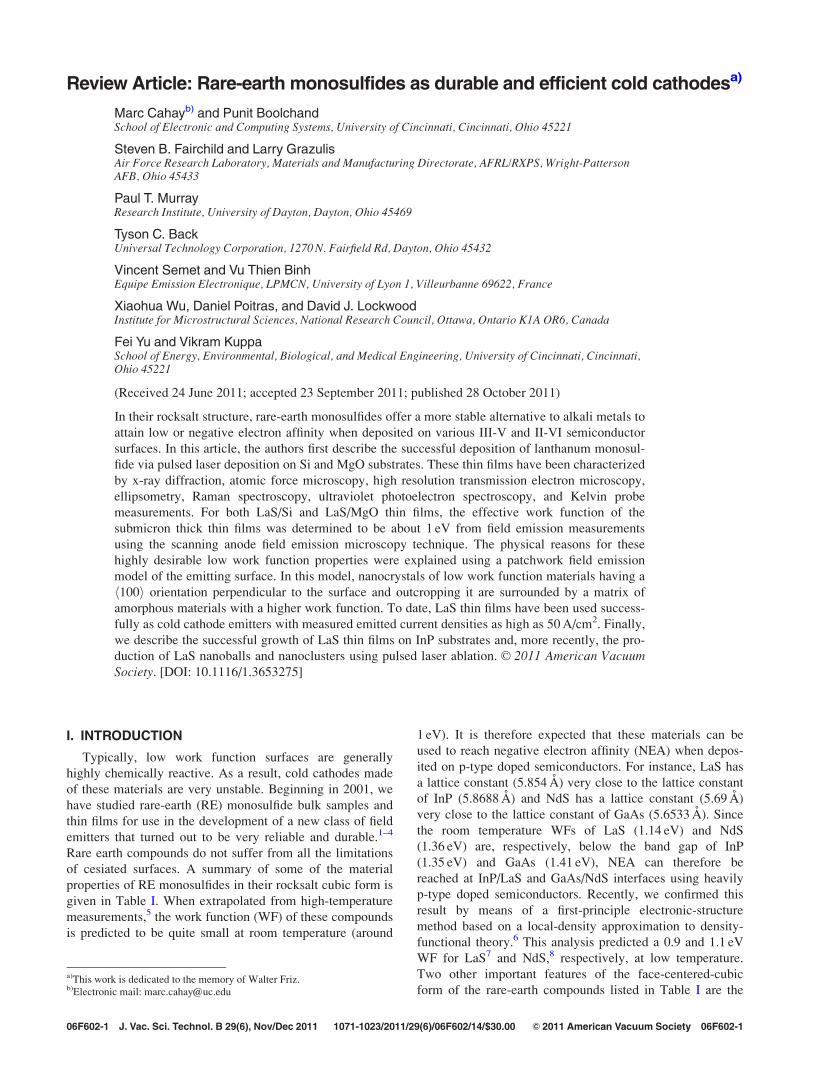
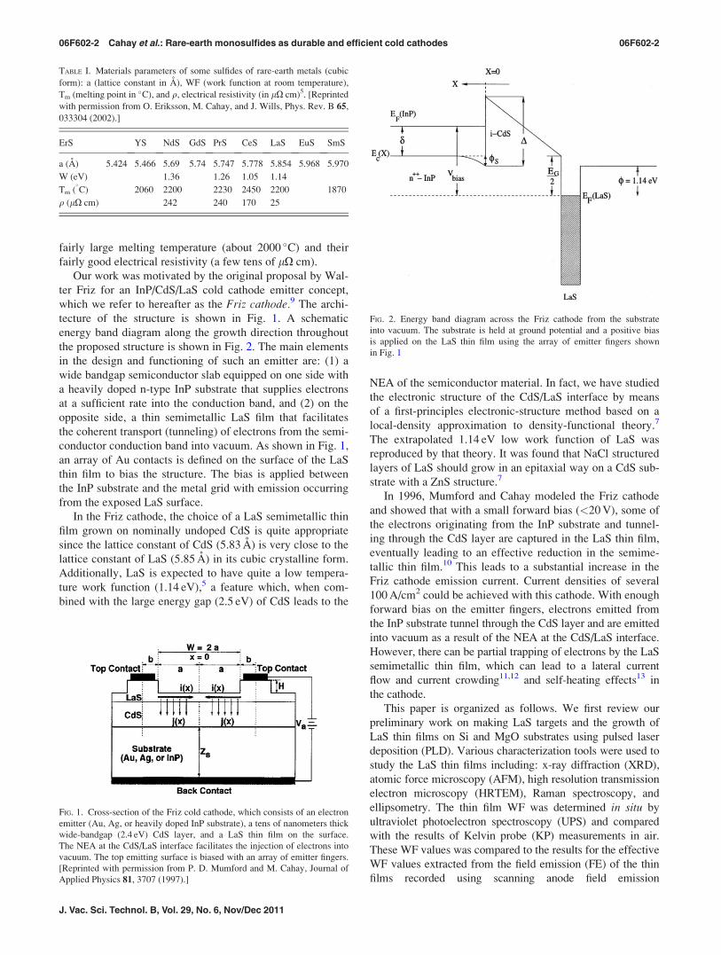
Our work was motivated by the original proposal by Wal-
ter Friz for an InP/CdS/LaS cold cathode emitter concept,
which we refer to hereafter as the Friz cathode.9 The archi-
tecture of the structure is shown in Fig. 1. A schematic
energy band diagram along the growth direction throughout
the proposed structure is shown in Fig. 2. The main elements
in the design and functioning of such an emitter are: (1) a
wide bandgap semiconductor slab equipped on one side with
a heavily doped n-type InP substrate that supplies electrons
at a sufficient rate into the conduction band, and (2) on the
opposite side, a thin semimetallic LaS film that facilitates
the coherent transport (tunneling) of electrons from the semi-
conductor conduction band into vacuum. As shown in Fig. 1,
an array of Au contacts is defined on the surface of the LaS
thin film to bias the structure. The bias is applied between
the InP substrate and the metal grid with emission occurring
from the exposed LaS surface.
In the Friz cathode, the choice of a LaS semimetallic thin
film grown on nominally undoped CdS is quite appropriate
since the lattice constant of CdS (5.83 A) is very close to the
lattice constant of LaS (5.85 A) in its cubic crystalline form.
Additionally, LaS is expected to have quite a low tempera-
ture work function (1.14 eV),5 a feature which, when com-
bined with the large energy gap (2.5 eV) of CdS leads to the
NEA of the semiconductor material. In fact, we have studied
the electronic structure of the CdS/LaS interface by means
of a first-principles electronic-structure method based on a
local-density approximation to density-functional theory.7
The extrapolated 1.14 eV low work function of LaS was
reproduced by that theory. It was found that NaCl structured
layers of LaS should grow in an epitaxial way on a CdS sub-
strate with a ZnS structure.7
In 1996, Mumford and Cahay modeled the Friz cathode
and showed that with a small forward bias (<20 V), some of
the electrons originating from the InP substrate and tunnel-
ing through the CdS layer are captured in the LaS thin film,
eventually leading to an effective reduction in the semime-
tallic thin film.10 This leads to a substantial increase in the
Friz cathode emission current. Current densities of several
100 A/cm2 could be achieved with this cathode. With enough
forward bias on the emitter fingers, electrons emitted from
the InP substrate tunnel through the CdS layer and are emitted
into vacuum as a result of the NEA at the CdS/LaS interface.
However, there can be partial trapping of electrons by the LaS
semimetallic thin film, which can lead to a lateral current
flow and current crowding11,12 and self-heating effects13 in
the cathode.
This paper is organized as follows. We first review our
preliminary work on making LaS targets and the growth of
LaS thin films on Si and MgO substrates using pulsed laser
deposition (PLD). Various characterization tools were used to
study the LaS thin films including: x-ray diffraction (XRD),
atomic force microscopy (AFM), high resolution transmission
electron microscopy (HRTEM), Raman spectroscopy, and
ellipsometry. The thin film WF was determined in situ by
ultraviolet photoelectron spectroscopy (UPS) and compared
with the results of Kelvin probe (KP) measurements in air.
These WF values was compared to the results for the effective
WF values extracted from the field emission (FE) of the thin
films recorded using scanning anode field emission
TABLE I. Materials parameters of some sulfides of rare-earth metals (cubic
form): a (lattice constant in A), WF (work function at room temperature),
Tm (melting point in �C), and q, electrical resistivity (in lX cm)5. [Reprinted
with permission from O. Eriksson, M. Cahay, and J. Wills, Phys. Rev. B 65,
033304 (2002).]
ErS YS NdS GdS PrS CeS LaS EuS SmS
a (A) 5.424 5.466 5.69 5.74 5.747 5.778 5.854 5.968 5.970
W (eV) 1.36 1.26 1.05 1.14
Tm (�C) 2060 2200 2230 2450 2200 1870
q (lX cm) 242 240 170 25
FIG. 1. Cross-section of the Friz cold cathode, which consists of an electron
emitter (Au, Ag, or heavily doped InP substrate), a tens of nanometers thick
wide-bandgap (2.4 eV) CdS layer, and a LaS thin film on the surface.
The NEA at the CdS/LaS interface facilitates the injection of electrons into
vacuum. The top emitting surface is biased with an array of emitter fingers.
[Reprinted with permission from P. D. Mumford and M. Cahay, Journal of
Applied Physics 81, 3707 (1997).]
FIG. 2. Energy band diagram across the Friz cathode from the substrate
into vacuum. The substrate is held at ground potential and a positive bias
is applied on the LaS thin film using the array of emitter fingers shown
in Fig. 1
06F602-2 Cahay et al.: Rare-earth monosulfides as durable and efficient cold cathodes 06F602-2
J. Vac. Sci. Technol. B, Vol. 29, No. 6, Nov/Dec 2011
microscopy (SAFEM). The low effective WF (�1 eV) of the
films was interpreted in terms of a recently developed patch-
work FE model of the emitting surface. The main ingredients
of the patchwork FE model and its practical implications are
emphasized. Finally, we describe the successful growth of
LaS thin films on InP substrates and, more recently, the pro-
duction of LaS nanoballs and nanoclusters using pulsed laser
ablation (PLA).
II. EXPERIMENT
In our PLD experiments1–4 the target to substrate distance
was set equal to about 10 cm and the vacuum chamber base
pressure was typically a few 10�8 Torr. A pulsed Lambda
Physik LPX 305 excimer laser operating at a wavelength
of 248 nm and a repetition rate up to 10 Hz was used for
the deposition. The beam spot size on target was about
4� 8 mm2 and the laser energy was estimated to be between
300 and 400 mJ/pulse. During deposition, the target was
rotated on axis while galvanometers were used to raster the
laser beam in a uniformly random pattern over the surface of
the target. This configuration produces a uniform laser plume
by preventing the uneven erosion of the target.
The XRD 2H scans were performed using a PanAlytical
X’Pert Pro x-ray diffraction system in which the incident
angle was set equal to 5�. Surface images were obtained by
AFM using a Pacific Nanotechnology Nano-R SPM (model
no. 0-200-002) operating in vibrating mode. Line scans were
performed to measure the surface roughness and the grain
size of the films was extracted using the Scherrer formula.14
The LaS films were characterized with a Staib multitech-
nique surface analysis system equipped with a DESA 150
double-pass cylindrical mirror analyzer. The background
pressure in the system was 3� 10�10 Torr. The binding
energy scale was calibrated against the Fermi edge of a sput-
ter cleaned Au sample. The UPS data were acquired using
the Specs 10/35 He I (21.22 eV) gas discharge lamp. Resolu-
tion was determined from the width of the Au Fermi edge,
which was found to be 250 meV. The sample was negatively
biased in order to determine the true work function of the
sample. The WF of the thin films was also measured in situusing a McCallister KP-6500 Kelvin probe with a stainless
steel tip with a 5 mm diameter. The procedure involved first
determining the WF of the tip using UPS. The WF tip value
was found to be 4.8 eV. The absolute value of the film WF
was then determined by the difference between the KP tip
and the sample as recorded in the KP experiments.
A variable-angle spectroscopic ellipsometer (VASE, J.A.
Woollam Co. Lincoln, NE) was used for the characterization
of the optical constants of the film in the near UV and visible
wavelength range.
To investigate the crystalline texture of the films, a h011icross-section TEM sample was prepared following standard
procedures. Two bars were cut out of a wafer, and were
glued together with the film sides face-to-face to make the
central part of a 3 mm diameter cross-section disc. Then the
disc was mechanically thinned to a thickness of �100 lm.
The thinned disc was dimpled from both sides with 3 lm dia-
mond paste until the center of the disc was �20 lm thick,
and then polished from both sides with 1 lm diamond paste
to obtain a very smooth surface. The final thinning until per-
foration was conducted using Ar ion-milling from both sides
using an ion beam angle of 8�, and a gun voltage of 6 kV.
The TEM sample was examined in a Philips EM430T oper-
ating at 250 kV.
The SAFEM technique was used to measure the current-
voltage (I-V) characteristics at different surface locations
and at different temperatures of a LaS thin film with an area
of about a 1 cm. For one location, the full set of measured
I-V characteristics (total measured current versus applied
voltage) for different values of Z, the distance between the
cathode surface and the probe ball, were then analyzed in
order to extract the current density, J, versus the actual
applied field, F (J-F) data.15,16
Raman measurements were performed at 295 K employ-
ing 1 mW of 488 nm light from a Picarro diode-pumped
solid state laser for excitation in a backscattering geometry
using the confocal microscope with a 100x objective on a
Jobin-Yvon T64000 triple spectrometer operated in the sub-
tractive mode. The incident laser light was focused on the
LaS layer.
A. Prior experimental work
1. RE target preparation
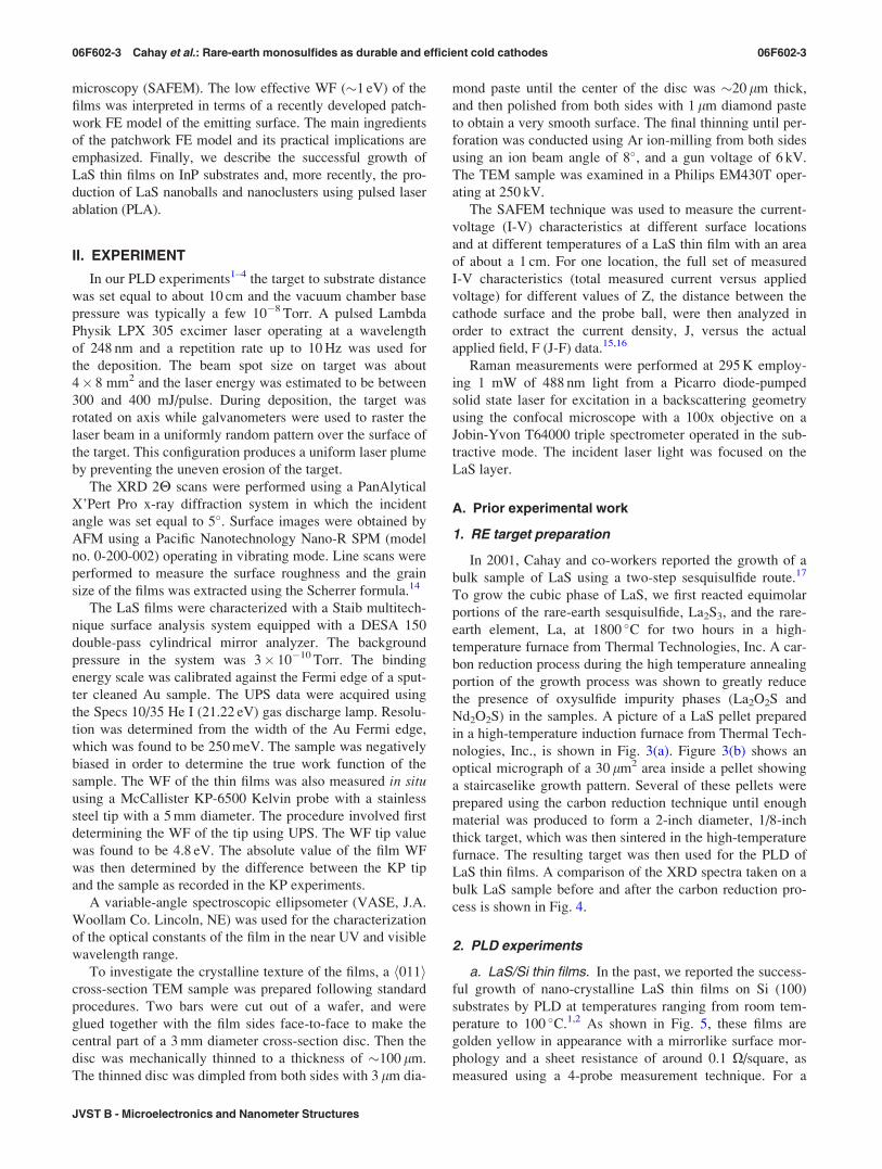
In 2001, Cahay and co-workers reported the growth of a
bulk sample of LaS using a two-step sesquisulfide route.17
To grow the cubic phase of LaS, we first reacted equimolar
portions of the rare-earth sesquisulfide, La2S3, and the rare-
earth element, La, at 1800 �C for two hours in a high-
temperature furnace from Thermal Technologies, Inc. A car-
bon reduction process during the high temperature annealing
portion of the growth process was shown to greatly reduce
the presence of oxysulfide impurity phases (La2O2S and
Nd2O2S) in the samples. A picture of a LaS pellet prepared
in a high-temperature induction furnace from Thermal Tech-
nologies, Inc., is shown in Fig. 3(a). Figure 3(b) shows an
optical micrograph of a 30 lm2 area inside a pellet showing
a staircaselike growth pattern. Several of these pellets were
prepared using the carbon reduction technique until enough
material was produced to form a 2-inch diameter, 1/8-inch
thick target, which was then sintered in the high-temperature
furnace. The resulting target was then used for the PLD of
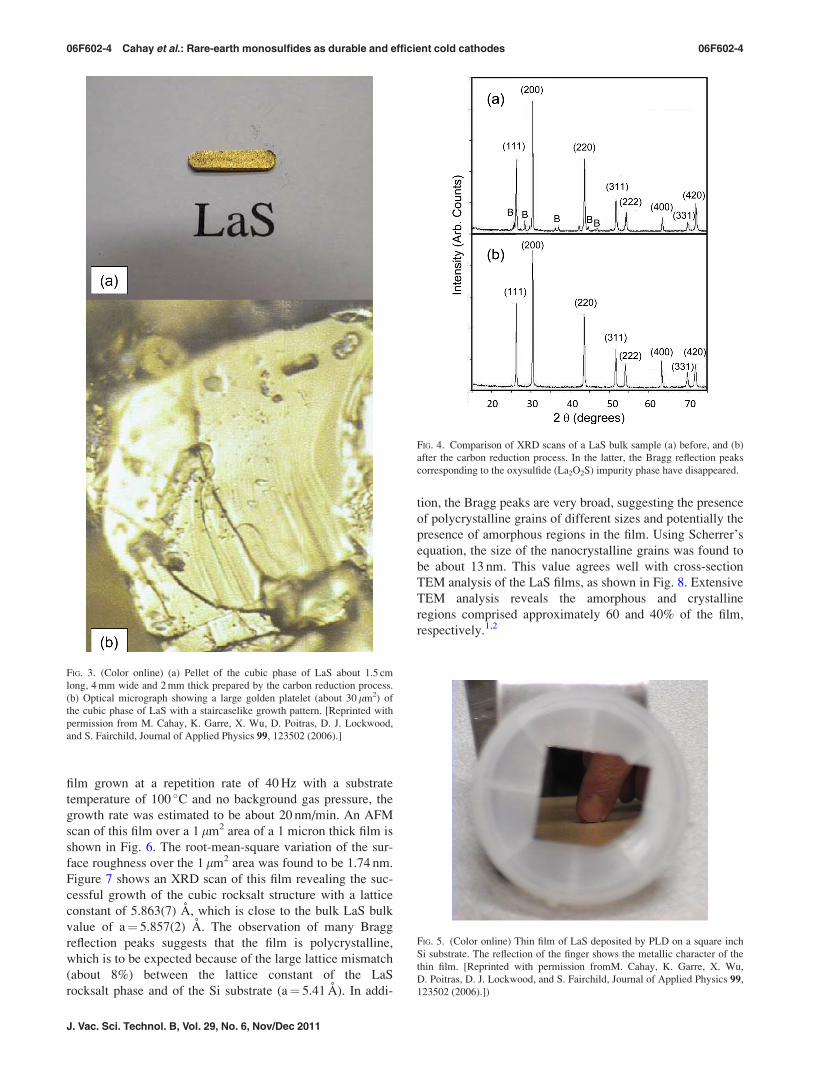
LaS thin films. A comparison of the XRD spectra taken on a
bulk LaS sample before and after the carbon reduction pro-
cess is shown in Fig. 4.
2. PLD experiments
a. LaS/Si thin films. In the past, we reported the success-
ful growth of nano-crystalline LaS thin films on Si (100)
substrates by PLD at temperatures ranging from room tem-
perature to 100 �C.1,2 As shown in Fig. 5, these films are
golden yellow in appearance with a mirrorlike surface mor-
phology and a sheet resistance of around 0.1 X/square, as
measured using a 4-probe measurement technique. For a
06F602-3 Cahay et al.: Rare-earth monosulfides as durable and efficient cold cathodes 06F602-3
JVST B - Microelectronics and Nanometer Structures
film grown at a repetition rate of 40 Hz with a substrate
temperature of 100 �C and no background gas pressure, the
growth rate was estimated to be about 20 nm/min. An AFM
scan of this film over a 1 lm2 area of a 1 micron thick film is
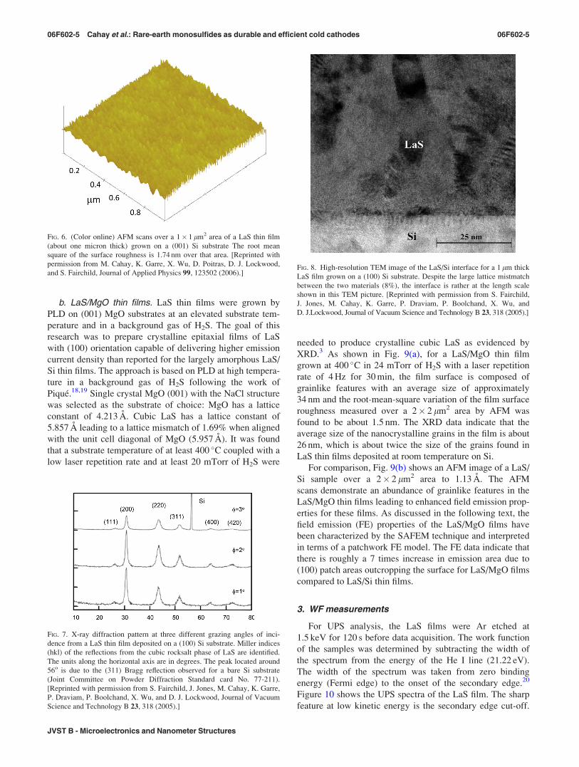
shown in Fig. 6. The root-mean-square variation of the sur-
face roughness over the 1 lm2 area was found to be 1.74 nm.
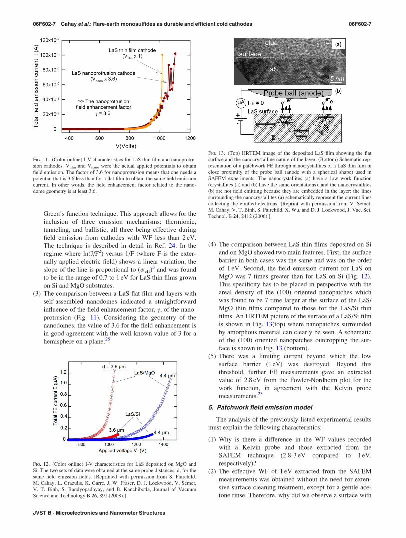
Figure 7 shows an XRD scan of this film revealing the suc-
cessful growth of the cubic rocksalt structure with a lattice
constant of 5.863(7) A, which is close to the bulk LaS bulk
value of a¼ 5.857(2) A. The observation of many Bragg
reflection peaks suggests that the film is polycrystalline,
which is to be expected because of the large lattice mismatch
(about 8%) between the lattice constant of the LaS
rocksalt phase and of the Si substrate (a¼ 5.41 A). In addi-
tion, the Bragg peaks are very broad, suggesting the presence
of polycrystalline grains of different sizes and potentially the
presence of amorphous regions in the film. Using Scherrer’s
equation, the size of the nanocrystalline grains was found to
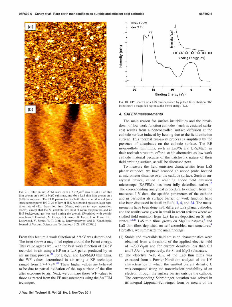
be about 13 nm. This value agrees well with cross-section
TEM analysis of the LaS films, as shown in Fig. 8. Extensive
TEM analysis reveals the amorphous and crystalline
regions comprised approximately 60 and 40% of the film,
respectively.1,2
FIG. 3. (Color online) (a) Pellet of the cubic phase of LaS about 1.5 cm
long, 4 mm wide and 2 mm thick prepared by the carbon reduction process.
(b) Optical micrograph showing a large golden platelet (about 30 lm2) of
the cubic phase of LaS with a staircaselike growth pattern. [Reprinted with
permission from M. Cahay, K. Garre, X. Wu, D. Poitras, D. J. Lockwood,
and S. Fairchild, Journal of Applied Physics 99, 123502 (2006).]
FIG. 4. Comparison of XRD scans of a LaS bulk sample (a) before, and (b)
after the carbon reduction process. In the latter, the Bragg reflection peaks
corresponding to the oxysulfide (La2O2S) impurity phase have disappeared.
FIG. 5. (Color online) Thin film of LaS deposited by PLD on a square inch
Si substrate. The reflection of the finger shows the metallic character of the
thin film. [Reprinted with permission fromM. Cahay, K. Garre, X. Wu,
D. Poitras, D. J. Lockwood, and S. Fairchild, Journal of Applied Physics 99,
123502 (2006).])
06F602-4 Cahay et al.: Rare-earth monosulfides as durable and efficient cold cathodes 06F602-4
J. Vac. Sci. Technol. B, Vol. 29, No. 6, Nov/Dec 2011
b. LaS/MgO thin films. LaS thin films were grown by
PLD on (001) MgO substrates at an elevated substrate tem-
perature and in a background gas of H2S. The goal of this
research was to prepare crystalline epitaxial films of LaS
with (100) orientation capable of delivering higher emission
current density than reported for the largely amorphous LaS/
Si thin films. The approach is based on PLD at high tempera-
ture in a background gas of H2S following the work of
Pique.18,19 Single crystal MgO (001) with the NaCl structure
was selected as the substrate of choice: MgO has a lattice
constant of 4.213 A. Cubic LaS has a lattice constant of
5.857 A leading to a lattice mismatch of 1.69% when aligned
with the unit cell diagonal of MgO (5.957 A). It was found
that a substrate temperature of at least 400 �C coupled with a
low laser repetition rate and at least 20 mTorr of H2S were
needed to produce crystalline cubic LaS as evidenced by
XRD.3 As shown in Fig. 9(a), for a LaS/MgO thin film
grown at 400 �C in 24 mTorr of H2S with a laser repetition
rate of 4 Hz for 30 min, the film surface is composed of
grainlike features with an average size of approximately
34 nm and the root-mean-square variation of the film surface
roughness measured over a 2� 2 lm2 area by AFM was
found to be about 1.5 nm. The XRD data indicate that the
average size of the nanocrystalline grains in the film is about
26 nm, which is about twice the size of the grains found in
LaS thin films deposited at room temperature on Si.
For comparison, Fig. 9(b) shows an AFM image of a LaS/
Si sample over a 2� 2 lm2 area to 1.13 A. The AFM
scans demonstrate an abundance of grainlike features in the
LaS/MgO thin films leading to enhanced field emission prop-
erties for these films. As discussed in the following text, the
field emission (FE) properties of the LaS/MgO films have
been characterized by the SAFEM technique and interpreted
in terms of a patchwork FE model. The FE data indicate that
there is roughly a 7 times increase in emission area due to
(100) patch areas outcropping the surface for LaS/MgO films
compared to LaS/Si thin films.
3. WF measurements
For UPS analysis, the LaS films were Ar etched at
1.5 keV for 120 s before data acquisition. The work function
of the samples was determined by subtracting the width of
the spectrum from the energy of the He I line (21.22 eV).
The width of the spectrum was taken from zero binding
energy (Fermi edge) to the onset of the secondary edge.20
Figure 10 shows the UPS spectra of the LaS film. The sharp
feature at low kinetic energy is the secondary edge cut-off.
FIG. 6. (Color online) AFM scans over a 1� 1 lm2 area of a LaS thin film
(about one micron thick) grown on a (001) Si substrate The root mean
square of the surface roughness is 1.74 nm over that area. [Reprinted with
permission from M. Cahay, K. Garre, X. Wu, D. Poitras, D. J. Lockwood,
and S. Fairchild, Journal of Applied Physics 99, 123502 (2006).]
FIG. 7. X-ray diffraction pattern at three different grazing angles of inci-
dence from a LaS thin film deposited on a (100) Si substrate. Miller indices
(hkl) of the reflections from the cubic rocksalt phase of LaS are identified.
The units along the horizontal axis are in degrees. The peak located around
56o is due to the (311) Bragg reflection observed for a bare Si substrate
(Joint Committee on Powder Diffraction Standard card No. 77-211).
[Reprinted with permission from S. Fairchild, J. Jones, M. Cahay, K. Garre,
P. Draviam, P. Boolchand, X. Wu, and D. J. Lockwood, Journal of Vacuum
Science and Technology B 23, 318 (2005).]
FIG. 8. High-resolution TEM image of the LaS/Si interface for a 1 lm thick
LaS film grown on a (100) Si substrate. Despite the large lattice mistmatch
between the two materials (8%), the interface is rather at the length scale
shown in this TEM picture. [Reprinted with permission from S. Fairchild,
J. Jones, M. Cahay, K. Garre, P. Draviam, P. Boolchand, X. Wu, and
D. J.Lockwood, Journal of Vacuum Science and Technology B 23, 318 (2005).]
06F602-5 Cahay et al.: Rare-earth monosulfides as durable and efficient cold cathodes 06F602-5
JVST B - Microelectronics and Nanometer Structures
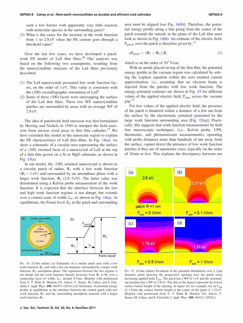
From this feature a work function of 2.9 eV was determined.
The inset shows a magnified region around the Fermi energy.
This value agrees well with the best work function of 2.6 eV
recorded in air using a KP on a LaS pellet produced by an
arc melting process.21 For LaS/Si and LaS/MgO thin films,
the WF values determined in air using a KP technique
ranged from 3.7-4.7 eV.22 These higher values are believed
to be due to partial oxidation of the top surface of the film
after exposure to air. Next, we compare these WF values to
those extracted from the FE measurements using the SAFEM
technique.
4. SAFEM measurements
The main reason for surface instabilities and the break-
down of low work function cathodes (such as cesiated surfa-
ces) results from a noncontrolled surface diffusion at the
cathode surface induced by heating due to the field emission
current. This thermal run-away process is amplified by the
presence of adsorbates on the cathode surface. The RE
monosulfide thin films, such as LaS/Si and LaS/MgO, in
their rocksalt structure, offer a stable alternative as low work
cathode material because of the patchwork nature of their
field emitting surface, as will be discussed next.
To measure the field emission characteristic from LaS
planar cathodes, we have scanned an anode probe located
at micrometer distance over the cathode surface. Such an an-
alytical device, called a scanning anode field emission
microscope (SAFEM), has been fully described earlier.15
The corresponding analytical procedure to extract, from the
measured I-V data, the specific parameters of the cathode
and in particular its surface barrier or work function have
also been discussed in detail in Refs. 3, 4, and 24. The meas-
urements have been done with different LaS planar cathodes,
and the results were given in detail in recent articles where we
studied field emission from LaS layers deposited on Si sub-
strates,1,2,23 LaS thin films grown on MgO substrates,3 and
LaS thin films deposited on self-assembled nanostructures.4
Hereafter, we summarize the main findings:
(1) Stable and reversible field emission characteristics were
obtained from a threshold of the applied electric field
of �230 V/lm and for current densities less than 0.3
and 7 A/cm2, respectively, for Si and MgO substrates.
(2) The effective WF, /eff, of the LaS thin films was
extracted from a Fowler-Nordheim analysis of the I-V
characteristics in which the emitted current density, J,
was computed using the transmission probability of an
electron through the surface barrier outside the cathode.
The corresponding Schrodinger equation was solved in
its integral Lippman-Schwinger form by means of the
FIG. 9. (Color online) AFM scans over a 2� 2 lm2 area of (a) a LaS thin
film grown on a (001) MgO substrate, and (b) a LaS thin film grown on a
(100) Si substrate. The PLD parameters for both films were identical (sub-
strate temperature: 400 C, 24 mTorr of H2S background pressure, laser repe-
tition rate of 4 Hz, deposition time: 30 min, substrate to target separation:
10 cm), except that the Si substrate was held at room temperature and no
H2S background gas was used during the growth. [Reprinted with permis-
sion from S. Fairchild, M. Cahay, L. Grazulis, K. Garre, J. W. Fraser, D. J.
Lockwood, V. Semet, V. T. Binh, S. Bandyopadhyay, and B. Kanchibotla,
Journal of Vacuum Science and Technology B 26, 891 (2008).]
FIG. 10. UPS spectra of a LaS film deposited by pulsed laser ablation. The
inset shows a magnified region at the Fermi energy (EF).
06F602-6 Cahay et al.: Rare-earth monosulfides as durable and efficient cold cathodes 06F602-6
J. Vac. Sci. Technol. B, Vol. 29, No. 6, Nov/Dec 2011
Green’s function technique. This approach allows for the
inclusion of three emission mechanisms: thermionic,
tunneling, and ballistic, all three being effective during
field emission from cathodes with WF less than 2 eV.
The technique is described in detail in Ref. 24. In the
regime where ln(J/F2) versus 1/F (where F is the exter-
nally applied electric field) shows a linear variation, the
slope of the line is proportional to (/eff)3 and was found
to be in the range of 0.7 to 1 eV for LaS thin films grown
on Si and MgO substrates.
(3) The comparison between a LaS flat film and layers with
self-assembled nanodomes indicated a straightforward
influence of the field enhancement factor, c, of the nano-
protrusion (Fig. 11). Considering the geometry of the
nanodomes, the value of 3.6 for the field enhancement is
in good agreement with the well-known value of 3 for a
hemisphere on a plane.25
(4) The comparison between LaS thin films deposited on Si
and on MgO showed two main features. First, the surface
barrier in both cases was the same and was on the order
of 1 eV. Second, the field emission current for LaS on
MgO was 7 times greater than for LaS on Si (Fig. 12).
This specificity has to be placed in perspective with the
areal density of the (100) oriented nanopatches which
was found to be 7 time larger at the surface of the LaS/
MgO thin films compared to those for the LaS/Si thin
films. An HRTEM picture of the surface of a LaS/Si film
is shown in Fig. 13(top) where nanopatches surrounded
by amorphous material can clearly be seen. A schematic
of the (100) oriented nanopatches outcropping the sur-
face is shown in Fig. 13 (bottom).
(5) There was a limiting current beyond which the low
surface barrier (1 eV) was destroyed. Beyond this
threshold, further FE measurements gave an extracted
value of 2.8 eV from the Fowler-Nordheim plot for the
work function, in agreement with the Kelvin probe
measurements.23
5. Patchwork field emission model
The analysis of the previously listed experimental results
must explain the following characteristics:
(1) Why is there a difference in the WF values recorded
with a Kelvin probe and those extracted from the
SAFEM technique (2.8-3 eV compared to 1 eV,
respectively)?
(2) The effective WF of 1 eV extracted from the SAFEM
measurements was obtained without the need for exten-
sive surface cleaning treatment, except for a gentle ace-
tone rinse. Therefore, why did we observe a surface with
FIG. 11. (Color online) I-V characteristics for LaS thin film and nanoprotru-
sion cathodes. Vfilm and Vnano were the actual applied potentials to obtain
field emission. The factor of 3.6 for nanoprotrusion means that one needs a
potential that is 3.6 less than for a flat film to obtain the same field emission
current. In other words, the field enhancement factor related to the nano-
dome geometry is at least 3.6.
FIG. 12. (Color online) I-V characteristics for LaS deposited on MgO and
Si. The two sets of data were obtained at the same probe distances, d, for the
same field emission fields. [Reprinted with permission from S. Fairchild,
M. Cahay, L. Grazulis, K. Garre, J. W. Fraser, D. J. Lockwood, V. Semet,
V. T. Binh, S. Bandyopadhyay, and B. Kanchibotla, Journal of Vacuum
Science and Technology B 26, 891 (2008).]
FIG. 13. (Top) HRTEM image of the deposited LaS film showing the flat
surface and the nanocrystalline nature of the layer. (Bottom) Schematic rep-
resentation of a patchwork FE through nanocrystallites of a LaS thin film in
close proximity of the probe ball (anode with a spherical shape) used in
SAFEM experiments. The nanocrystallites (a) have a low work function
(crystallites (a) and (b) have the same orientations), and the nanocrystallites
(b) are not field emitting because they are embedded in the layer; the lines
surrounding the nanocrystallites (a) schematically represent the current lines
collecting the emitted electrons. [Reprint with permission from V. Semet,
M. Cahay, V. T. Binh, S. Fairchild, X. Wu, and D. J. Lockwood, J. Vac. Sci.
Technol. B 24, 2412 (2006).]
06F602-7 Cahay et al.: Rare-earth monosulfides as durable and efficient cold cathodes 06F602-7
JVST B - Microelectronics and Nanometer Structures
such a low barrier with apparently very little reaction
with molecular species in the surrounding gases?
(3) What is the cause for the increase in the work function
from 1 to 2.8 eV when the FE current goes through a
threshold value?
Over the last few years, we have developed a patch-
work FE model of LaS thin films.26 Our analysis was
based on the following two assumptions, resulting from
the nanocrystalline structure of the LaS films previously
described:
(1) The LaS nanocrystals presented low work function fac-
ets, on the order of 1 eV. This value is consistent with
the (100) crystallographic orientation of LaS6.
(2) Some of these (100) facets were outcropping the surface
of the LaS thin films. These low WF nanocrystalline
patches are surrounded by areas with an average WF of
2.8 eV.
The idea of patchwork field emission was first formulated
by Herring and Nichols in 1949 to interpret the field emis-
sion from micron sized areas in thin film cathodes.27 We
have extended this model to the nanoscale region to explain
the FE characteristics of LaS thin films. In Fig. 14(a), we
show a schematic of a circular area representing the surface
of a h100i oriented facet of a nanocrystal of LaS at the top
of a thin film grown on a Si or MgO substrate, as shown in
Fig. 13(a).
In our model, the h100i oriented nanocrystal is shown as
a circular patch of radius, R, with a low work function
(U1� 1 eV) and surrounded by an amorphous phase with a
larger work function, U2 (2.8–3 eV). The latter value was
determined using a Kelvin probe measurement of the work
function. It is expected that the interface between the low
and high work function regions is not abrupt, but extends
over a contact zone of width, LC, as shown in Fig. 14(a). At
equilibrium, the Fermi level, Ef, in the patch and surrounding
area must be aligned [see Fig. 14(b)]. Therefore, the poten-
tial energy profile along a line going from the center of the
patch towards the outside in the plane of the LaS film must
look as shown in Fig. 14(b). An estimate of the electric field,
Fpatch, over the patch is therefore given by,15
eFpatch ¼ ðU2 � U1Þ=R; (1)
which is on the order of 107 V/cm.
With an anode placed on top of the thin film, the potential
energy profile in the vacuum region was calculated by solv-
ing the Laplace equation within the zero emitted current
approximation, i.e., assuming that no electron beam is
injected from the patches with low work function. The
energy potential contours are shown in Fig. 15 for different
values of the applied electric field, Fapp, across the vacuum
gap.23
For low values of the applied electric field, the presence
of the patch is hindered within a distance of a few nm from
the surface by the electrostatic potential generated by the
large work function surrounding area [Fig. 15(a)]. Practi-
cally, this suggests that work function measurements by field
free macroscopic techniques, (i.e., Kelvin probe, UPS,
thermionic, and photoemission measurements), operating
with probe distances more than hundreds of nm away from
the surface, cannot detect the presence of low work function
patches if they are of nanometer sizes, typically on the order
of 10 nm or less. This explains the discrepancy between our
FIG. 14. (Color online) (a) Schematic of a similar patch area with a low
work function, U1, and with a few nm diameter surrounded by a larger work
function, U2, amorphous phase. The separation between the two regions is
not abrupt and the work function linearly increases from U1 to U2 over a
connecting layer of width, LC, around 0.5 nm. [Reprint with permission
from V. T. Binh, R. Mouton, Ch. Adessi, V. Semet, M. Cahay, and S. Fair-
child, J. Appl. Phys. 108, 044311 (2010).] (b) Schematic of potential energy
profile at equilibrium at the interface between the central patch with low
work function, U1, and the surrounding amorphous material with a larger
work function, U2.
FIG. 15. (Color online) Evolution of the potential distribution over a 2 nm
diameter patch showing the progressive opening over the patch foran
increasing applied field, Fapp. The patch has a WF of 1 eV and the surround-
ing medium has a WF of 2.8 eV. The data in the figures represent the lowest
surface barrier height of the opening. In figure (d), for example, for an Fapp
of 1 V/nm the surface barrier height at the center of the patch is 1.32 eV.
[Reprint with permission from V. T. Binh, R. Mouton, Ch. Adessi, V.
Semet, M. Cahay, and S. Fairchild, J. Appl. Phys. 108, 044311 (2010).]
06F602-8 Cahay et al.: Rare-earth monosulfides as durable and efficient cold cathodes 06F602-8
J. Vac. Sci. Technol. B, Vol. 29, No. 6, Nov/Dec 2011
work function measurements by the Kelvin probe and FE
characteristics. Moreover, the potential screening of the low
work function nanopatches by the surrounding high work
function medium was sufficiently efficient to prevent
strong surface chemical adsorption occurring on as-grown
pristine LaS cathodes; therefore, allowing for the possibility
to obtain FE without any prior thermal or sputtering
treatments.
Eventually, the electrostatic opening of the patch occurs
when the contribution of the externally applied field counter-
balances the patch field estimated by Eq. (1), as shown in
Fig. 15. Therefore, the potential distribution over the patch is
dependent on the patch geometry, as illustrated in Fig. 16.
This means that the FE from the patch cathode will be
facilitated with an increase in the dimension of the patch,
asymptotically reaching the classical behavior of two inde-
pendent areas having, respectively, WFs of 1 and 2.8 eV.
However, an increase in the patch dimension in order
to increase the FE current must be balanced by the electro-
static potential protection of the patch by the high WF sur-
rounding area in order to keep the patch surface free from
adsorbates. This limits the size of the patch to an upper value
of 100 nm.
From the progressive opening of the patch, the I-V char-
acteristics from the patchwork cathode will first be governed
by the progressive field emission from the patch until the be-
ginning of the field emission from the surrounding region.
Considering the difference in WF values between these two
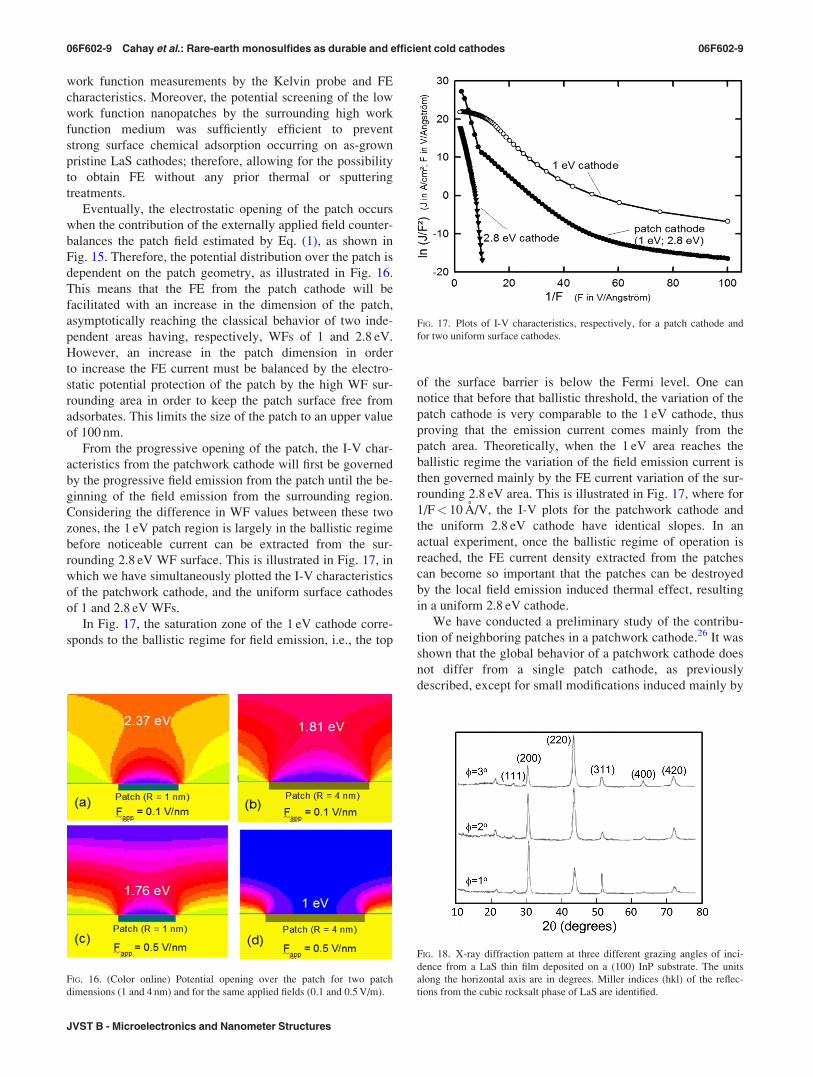
zones, the 1 eV patch region is largely in the ballistic regime
before noticeable current can be extracted from the sur-
rounding 2.8 eV WF surface. This is illustrated in Fig. 17, in
which we have simultaneously plotted the I-V characteristics
of the patchwork cathode, and the uniform surface cathodes
of 1 and 2.8 eV WFs.
In Fig. 17, the saturation zone of the 1 eV cathode corre-
sponds to the ballistic regime for field emission, i.e., the top
of the surface barrier is below the Fermi level. One can
notice that before that ballistic threshold, the variation of the
patch cathode is very comparable to the 1 eV cathode, thus
proving that the emission current comes mainly from the
patch area. Theoretically, when the 1 eV area reaches the
ballistic regime the variation of the field emission current is
then governed mainly by the FE current variation of the sur-
rounding 2.8 eV area. This is illustrated in Fig. 17, where for
1/F< 10 A/V, the I-V plots for the patchwork cathode and
the uniform 2.8 eV cathode have identical slopes. In an
actual experiment, once the ballistic regime of operation is
reached, the FE current density extracted from the patches
can become so important that the patches can be destroyed
by the local field emission induced thermal effect, resulting
in a uniform 2.8 eV cathode.
We have conducted a preliminary study of the contribu-
tion of neighboring patches in a patchwork cathode.26 It was
shown that the global behavior of a patchwork cathode does
not differ from a single patch cathode, as previously
described, except for small modifications induced mainly by
FIG. 16. (Color online) Potential opening over the patch for two patch
dimensions (1 and 4 nm) and for the same applied fields (0.1 and 0.5 V/m).
FIG. 17. Plots of I-V characteristics, respectively, for a patch cathode and
for two uniform surface cathodes.
FIG. 18. X-ray diffraction pattern at three different grazing angles of inci-
dence from a LaS thin film deposited on a (100) InP substrate. The units
along the horizontal axis are in degrees. Miller indices (hkl) of the reflec-
tions from the cubic rocksalt phase of LaS are identified.
06F602-9 Cahay et al.: Rare-earth monosulfides as durable and efficient cold cathodes 06F602-9
JVST B - Microelectronics and Nanometer Structures
the coupling of the potential distribution between patches.
The overall potential distribution over an array of patches
keeps the same progressive barrier opening with the exter-
nally applied field above each individual patch. As a result,
a nanopatchwork cathode will preferentially emit from an
array of parallel e-beams strictly localized over the low WF
patches. On a real polycrystalline surface, the patch distri-
bution is more erratic. Therefore, more work is needed to
gain control over the patch size and location to study the op-
timum conditions under which the low WF nanopatches
stay protected from contamination by the surrounding
material with a larger WF. A well regimented nanopatch
structure would allow the emission of nondiffracted
parallel nanosized e-beams with well-defined locations
which would provide a new route for coherent parallel
e-beam applications.
B. Recent experimental work
1. Growth of LaS thin films on InP substrates
The LaS thin films were grown by PLD on (100) oriented
InP substrates at room temperature using the following PLD
parameters: repetition rate¼ 4 Hz, laser energy¼ 850 mJ/
pulse, and duration¼ 30 min. Figure 18 shows the x-ray dif-
fraction pattern recorded at three different grazing angles of
incidence. Miller indices (hkl) of the reflections from the
cubic rocksalt phase of LaS are identified. The Bragg reflec-
tion peaks are narrower than those for a LaS thin film on a Si
substrate, as shown in Fig. 7, indicating a much higher level
of crystallinity in the Las/InP film due to the closer lattice-
match between the two materials.
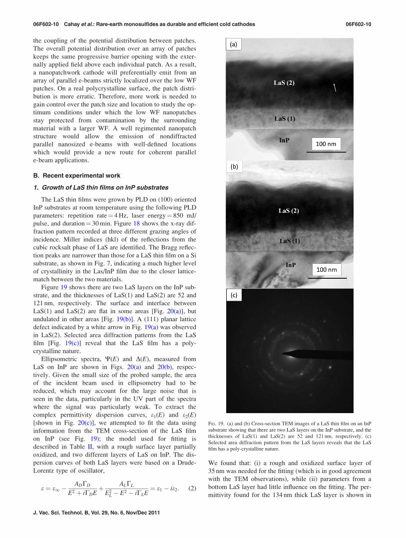
Figure 19 shows there are two LaS layers on the InP sub-
strate, and the thicknesses of LaS(1) and LaS(2) are 52 and
121 nm, respectively. The surface and interface between
LaS(1) and LaS(2) are flat in some areas [Fig. 20(a)], but
undulated in other areas [Fig. 19(b)]. A (111) planar lattice
defect indicated by a white arrow in Fig. 19(a) was observed
in LaS(2). Selected area diffraction patterns from the LaS
film [Fig. 19(c)] reveal that the LaS film has a poly-
crystalline nature.
Ellipsometric spectra, W(E) and D(E), measured from
LaS on InP are shown in Figs. 20(a) and 20(b), respec-
tively. Given the small size of the probed sample, the area
of the incident beam used in ellipsometry had to be
reduced, which may account for the large noise that is
seen in the data, particularly in the UV part of the spectra
where the signal was particularly weak. To extract the
complex permittivity dispersion curves, e1(E) and e2(E)
[shown in Fig. 20(c)], we attempted to fit the data using
information from the TEM cross-section of the LaS film
on InP (see Fig. 19); the model used for fitting is
described in Table II, with a rough surface layer partially
oxidized, and two different layers of LaS on InP. The dis-
persion curves of both LaS layers were based on a Drude-
Lorentz type of oscillator,
e ¼ e1 �ADCD
E2 þ iCDEþ ALCL
E2L � E2 � iCLE
¼ e1 � ie2: (2)
We found that: (i) a rough and oxidized surface layer of
35 nm was needed for the fitting (which is in good agreement
with the TEM observations), while (ii) parameters from a
bottom LaS layer had little influence on the fitting. The per-
mittivity found for the 134 nm thick LaS layer is shown in
FIG. 19. (a) and (b) Cross-section TEM images of a LaS thin film on an InP
substrate showing that there are two LaS layers on the InP substrate, and the
thicknesses of LaS(1) and LaS(2) are 52 and 121 nm, respectively. (c)
Selected area diffraction pattern from the LaS layers reveals that the LaS
film has a poly-crystalline nature.
06F602-10 Cahay et al.: Rare-earth monosulfides as durable and efficient cold cathodes 06F602-10
J. Vac. Sci. Technol. B, Vol. 29, No. 6, Nov/Dec 2011
Fig. 20(c); the incident light energy value for which e1
equals zero (2.53 eV) corresponds to the plasma frequency
below which the material starts behaving as a metal. Figure
20(d) shows the estimated penetration depth of the light into
the LaS film based on the permittivity dispersion; it can be
seen that below 3.5 eV, the light is not expected to reach the
bottom LaS layer found on the TEM micrograph, which
explains the small impact of this layer in our model, and is a
typical metallic behavior.
Using a Drude model only [the first two terms of Eq. (2)],
we re-fitted the portion of the data corresponding to the me-
tallic region (energy values below the plasmon frequency),
and estimated a carrier concentration and a mobility of
8.44� 1022 cm�3 and 1.42 cm2 V�1 s�1, respectively
(assuming an effective mass, m*¼ 1.3) for the 134 nm thick
LaS layer, and a resistivity of 5.22� 10�5 X cm�1 for that
same layer.
The Raman spectra of the LaS/InP films exhibit weak
broad features extending out to 600 cm�1, as illustrated in
Fig. 21. Figure 20(d) shows that the Raman excitation light
at 488 nm has a penetration depth of only 30 nm in the film.
The results obtained are generally similar, but not in detail,
to those found from Raman measurements on bulk pure LaS
samples (see Fig. 21), confirming that the LaS films are of
the pure cubic form. Strong peaks are observed at about 86
and 108 cm�1, with weaker features at 178, 198, 261, 301,
347, 448, and 518 cm�1.
One triply-degenerate optical phonon mode, split into
longitudinal (LO) and transverse (TO) components, is
expected for rare-earth monochalcogenides possessing the
rocksalt crystal structure. First-order Raman scattering from
phonons in such crystals is symmetry forbidden and usually
a weak second-order Raman spectra is observed reflecting
the two-phonon density of states (DOS). However, previous
Raman studies of other rare earth chalcogenides9,29 have
shown that disorder introduced by defects such as cation
and/or anion vacancies9 can induce a first-order Raman spec-
trum reflecting the one-phonon DOS. The TEM analysis of
our samples shows that structural disorder due to the forma-
tion of nanocrystals separated by amorphous material is also
present. Thus, the Raman spectrum of our LaS films can be
expected to show both disorder-induced first-order and
FIG. 20. (a) and (b) Ellipsometric spectra, W(E) and D(E), measured from
LaS on InP, respectively. (c) The extracted complex permittivity dispersion
curves, e1(E) and e2(E). (d) The estimated penetration depth of the light into
the LaS film based on the permittivity dispersion.
TABLE II. Model used for fitting the ellipsometric data for a film of LaS on
InP.
Layer Description Thickness
Top layer Rough oxidized layer 35.4 nm
Layer 2 Top LaS layer 134.7 nm
Layer 1 Bottom LaS layer 52.0 nm
Layer 0 InP substrate 0.5 mm
FIG. 21. Room temperature Raman spectrum of (a) bulk LaS (from a target
similar to that used in the growth chamber) compared with (b) a LaS film
grown on (100) InP. Here, A and O refer to acoustic and optical phonons
involved in first-order and second-order Raman scattering.
06F602-11 Cahay et al.: Rare-earth monosulfides as durable and efficient cold cathodes 06F602-11
JVST B - Microelectronics and Nanometer Structures
second-order Raman features. In fact, our results for LaS
films on InP resemble those previously obtained for LaS
films on Si.2 However, a closer examination of Fig. 21 shows
that the Raman spectra of the present samples are quantita-
tively different from that of bulk LaS:30 the Raman peaks
above �150 cm�1 are much weaker and more diffuse than
those found in bulk LaS and no sharp features are seen at
106, 178, and 189 cm�1. This is consistent with disorder in
the LaS films.
The stronger features at 86 and 108 cm�1 are clearly due
to disorder induced first-order Raman scattering from acoustic
(A) phonons2,9,29,30 while the peak at 261 cm�1 similarly
arises from optic (O) phonons. Inelastic neutron scattering
measurements of the acoustic phonon dispersion in LaS
(Ref. 31) allow us to determine the origins of the acoustic
Raman features. The 86 cm�1 peak arises primarily from
transverse (TA) and longitudinal (LA) acoustic phonons
at the X and K critical points in the Brillouin zone, while the
shoulder at 108 cm�1 comes mainly from the L point TA
and LA phonons. The distinct O peak at 261 cm�1 comprises
contributions from both TO and LO phonons, with the
highest frequency contributions from LO modes.2 The broad
and very weak bands occurring at frequencies higher than the
optical phonon peak at 261 cm�1 are second-order in origin,
primarily reflecting combinations of the disorder-induced
first-order DOS Raman peaks. For example, the peaks at 347,
448, and 518 cm�1 can be attributed to the combinations of
the 86 and 108 (A) cm�1 peaks with the 261 (O) cm�1 peak
(AþO), 2 A/OþO and 2O, respectively (see Fig. 21).
2. Growth of LaS nanoballs and nanoclusters
Nanoclusters of LaS were fabricated by pulsed laser abla-
tion (PLA) of a LaS target (5 cm diameter) with the output
of a KrF (k¼ 248 nm) excimer laser. The laser pulse dura-
tion was 25 ns, and the laser energy was 700 mJ per pulse.
The target was rotated during deposition in order to expose a
fresh LaS surface to each successive ablating laser pulse.
Ablation was carried out in a static Ar background pressure
of 1 Torr. Nanoclusters were deposited on a Si substrate (for
SEM characterization) and on a TEM grid, both of which
were situated 5 cm from the target. A total of four laser shots
were used to fabricate the TEM samples, while the samples
used for the SEM characterization were prepared by ablating
the LaS target for 5 min at a repetition rate of 10 Hz.
Synthesis of nanoclusters by PLA typically results in a bi-
modal size distribution.32 The smaller (1 nm< diameter
< 10 nm) nanoclusters are formed by recombination in the
gas phase of ablated atomic and molecular species. Larger
nanoclusters are directly ejected from the target by a process
denoted as splashing,33 which can be understood by consid-
ering the nature of the species ejected from the target as a
function of depth into the target. Species originating close to
the target surface are exposed to the full laser energy and are
ejected primarily as atoms; however, at great distances into
the target, the laser energy is attenuated to such an extent
that the target is heated rather than ablated. This results in
the ejection of molten nanodroplets of liquid target material.
Although splashing can be an inconvenience for the deposi-
tion of epitaxial thin films, we use it to our advantage in
nanocluster synthesis.
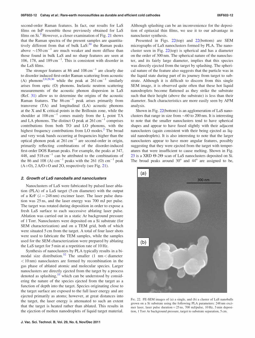
Presented in Figs. 22(top) and 22(bottom) are SEM
micrographs of LaS nanoclusters formed by PLA. The nano-
cluster seen in Fig. 22(top) is spherical and has a diameter
on the order of 300 nm. The spherical nature of the nanoclus-
ter, and its fairly large diameter, implies that this species
was directly ejected from the target by splashing. The spheri-
cal nature of the feature also suggests that the particle was in
the liquid state during part of its journey from target to sub-
strate. Although it is difficult to discern from this single
SEM image, it is observed quite often that these hot liquid
nanodroplets become flattened as they strike the substrate
such that their height (above the substrate) is less than their
diameter. Such characteristics are more easily seen by AFM
analysis.
Shown in Fig. 22(bottom) is an agglomeration of LaS nano-
clusters that range in size from �60 to 200 nm. It is interesting
to note that the smaller nanoclusters tend to have spherical
shapes and appear to have fused slightly with their adjacent
nanoclusters (again consistent with their being ejected as liq-
uid nanodroplets). It is also interesting to note that the larger
nanoclusters appear to have more angular features, possibly
suggesting that they were ejected from the target with temper-
atures that were insufficient to cause melting. Shown in Fig.
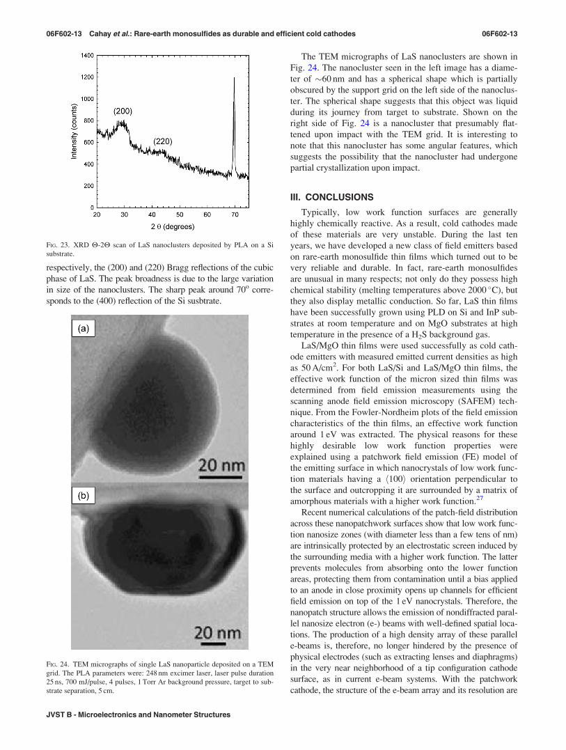
23 is a XRD H-2H scan of LaS nanoclusters deposited on Si.
The broad peaks around 30o and 44o are assigned to be,
FIG. 22. FE-SEM images of (a) a single, and (b) a cluster of LaS nanoballs
grown on a Si substrate using the following PLA parameters: 248 nm exci-
mer laser, laser pulse duration¼ 25 ns, 700 mJ/pulse, 10 Hz, 5 min deposi-
tion, 1 Torr Ar background pressure, target to substrate separation, 5 cm.
06F602-12 Cahay et al.: Rare-earth monosulfides as durable and efficient cold cathodes 06F602-12
J. Vac. Sci. Technol. B, Vol. 29, No. 6, Nov/Dec 2011
respectively, the (200) and (220) Bragg reflections of the cubic
phase of LaS. The peak broadness is due to the large variation
in size of the nanoclusters. The sharp peak around 70o corre-
sponds to the (400) reflection of the Si susbtrate.
The TEM micrographs of LaS nanoclusters are shown in
Fig. 24. The nanocluster seen in the left image has a diame-
ter of �60 nm and has a spherical shape which is partially
obscured by the support grid on the left side of the nanoclus-
ter. The spherical shape suggests that this object was liquid
during its journey from target to substrate. Shown on the
right side of Fig. 24 is a nanocluster that presumably flat-
tened upon impact with the TEM grid. It is interesting to
note that this nanocluster has some angular features, which
suggests the possibility that the nanocluster had undergone
partial crystallization upon impact.
III. CONCLUSIONS
Typically, low work function surfaces are generally
highly chemically reactive. As a result, cold cathodes made
of these materials are very unstable. During the last ten
years, we have developed a new class of field emitters based
on rare-earth monosulfide thin films which turned out to be
very reliable and durable. In fact, rare-earth monosulfides
are unusual in many respects; not only do they possess high
chemical stability (melting temperatures above 2000 �C), but
they also display metallic conduction. So far, LaS thin films
have been successfully grown using PLD on Si and InP sub-
strates at room temperature and on MgO substrates at high
temperature in the presence of a H2S background gas.
LaS/MgO thin films were used successfully as cold cath-
ode emitters with measured emitted current densities as high
as 50 A/cm2. For both LaS/Si and LaS/MgO thin films, the
effective work function of the micron sized thin films was
determined from field emission measurements using the
scanning anode field emission microscopy (SAFEM) tech-
nique. From the Fowler-Nordheim plots of the field emission
characteristics of the thin films, an effective work function
around 1 eV was extracted. The physical reasons for these
highly desirable low work function properties were
explained using a patchwork field emission (FE) model of
the emitting surface in which nanocrystals of low work func-
tion materials having a h100i orientation perpendicular to
the surface and outcropping it are surrounded by a matrix of
amorphous materials with a higher work function.27
Recent numerical calculations of the patch-field distribution
across these nanopatchwork surfaces show that low work func-
tion nanosize zones (with diameter less than a few tens of nm)
are intrinsically protected by an electrostatic screen induced by
the surrounding media with a higher work function. The latter
prevents molecules from absorbing onto the lower function
areas, protecting them from contamination until a bias applied
to an anode in close proximity opens up channels for efficient
field emission on top of the 1 eV nanocrystals. Therefore, the
nanopatch structure allows the emission of nondiffracted paral-
lel nanosize electron (e-) beams with well-defined spatial loca-
tions. The production of a high density array of these parallel
e-beams is, therefore, no longer hindered by the presence of
physical electrodes (such as extracting lenses and diaphragms)
in the very near neighborhood of a tip configuration cathode
surface, as in current e-beam systems. With the patchwork
cathode, the structure of the e-beam array and its resolution are
FIG. 23. XRD H-2H scan of LaS nanoclusters deposited by PLA on a Si
substrate.
FIG. 24. TEM micrographs of single LaS nanoparticle deposited on a TEM
grid. The PLA parameters were: 248 nm excimer laser, laser pulse duration
25 ns, 700 mJ/pulse, 4 pulses, 1 Torr Ar background pressure, target to sub-
strate separation, 5 cm.
06F602-13 Cahay et al.: Rare-earth monosulfides as durable and efficient cold cathodes 06F602-13
JVST B - Microelectronics and Nanometer Structures
only determined by the location and dimension of the nano-
patches over a plane surface, opening a new route for coherent
parallel e-beam applications.
More recently, we have been able to produce LaS nano-
balls and nanoclusters by PLA. The latter can be used to con-
trol the density and size of the nanopatches to generate a
high density of parallel nanosize electron-beams.
ACKNOWLEDGMENTS
The work at the University of Cincinnati was supported by
NSF Grant Nos, ECS-990653, ECS-9632511, and collaborative
Grant No. GOALI-ECS-0523966. Part of this work was per-
formed by M. Cahay under support from the Air Force Summer
Fellowship Program, Contract Nos. FA9550-07-C-0052 and
F49620-93-C-0063, and by Wright Laboratory. The work was
also supported by the Air Force Research Laboratory, Sensors,
Directorate, of Wright-Patterson Air Force Base under Contract
No. F33615-98-C-1204. The authors thank J.-M. Picard for
technical assistance with the Raman measurements.
1S. Fairchild, J. Jones, M. Cahay, K. Garre, P. Draviam, P. Boolchand, X.
Wu, and D. J. Lockwood, J. Vac. Sci. Technol. B 23, 318 (2005).2M. Cahay, K. Garre, X. Wu, D. Poitras, D. J. Lockwood, and S. Fairchild,
J. Appl. Phys. 99, 123502 (2006).3S. Fairchild, M. Cahay, L. Grazulis, K. Garre, J. W. Fraser, D. J. Lock-
wood, V. Semet, V. T. Binh, S. Bandyopadhyay, and B. Kanchibotla,
J. Vac. Sci. Technol. B 26, 891 (2008).4M. Cahay, K. Garre, V. Semet, V. T. Binh, J. W. Fraser, D. J. Lockwood,
S. Bandyopadhyay, S. Pramanik, B. Kanchibotla, S. Fairchild, and
L. Grazulis, J. Vac. Sci. Technol. B 25, 594 (2007).5The room-temperature work function for RE monosulfides listed in
Table I was calculated by extrapolating measured work function values at
high temperature as reported by S. Fomenko, in Handbook of ThermionicProperties (Plenum, New York, 1966). For RE monosulfides, the work
function increased with temperature at a rate of a few meV/K.6O. Eriksson, J. Willis, P. D. Mumford, M. Cahay, and W. Friz, Phys. Rev.
B 57, 4067 (1998).7O. Eriksson, M. Cahay, and J. Wills, Phys. Rev. B 65, 033304 (2002).
8O. Eriksson, M. Cahay, and J. Wills, “Negative electron affinity material:
NdS on GaAs,” (unpublished).9W. Friz, Final Technical Report: “Dynamic work function shift in current car-
rying thin films,” Task ELM-9, June 1992; Technical Note: “Cold Electron
Emitters,” Task ELM-6, January 1995; Progress Report: “More on Cold Elec-
tron Emitters,” Task ELM-11, June 1995, Wright-Patterson Air Force Base.10P. D. Mumford and M. Cahay, J. Appl. Phys. 79, 2176 (1996).11P. D. Mumford and M. Cahay, J. Appl. Phys. 81, 3707 (1997).12Y. Modukuru and M. Cahay, J. Vac. Sci. Technol. B 19, 2149 (2001).13A. Malhotra, Y. Modukuru, and M. Cahay, J. Vac. Sci. Technol. B 16,
3086 (1998).14C. Hammond, The Basics of Crystallography Diffraction (Oxford Univer-
sity Press, New York, 2003).15V. Semet, R. Mouton, and V. T. Binh, J. Vac. Sci. Technol. B 23, 671
(2005).16V. Semet, Ch. Adessi, T. Capron, and V. T. Binh, Phys. Rev B 75, 045430
(2007).17Y. Modukuru, J. Thachery, H. Tang, A. Malhotra, M. Cahay, and P.
Boolchand, J. Vac. Sci. Technol. B 19, 1958 (2001).18A. Pique, M. Mathur, J. Moses, and S. A. Mathews, Appl. Phys. Lett. 69,
391 (1996).19A. Pique, R. C. Auyeung, S. B. Qadri, H. Kim, B. L. Justus, and A. L.
Huston, Thin Solid Films 377-378, 803 (2000).20S. Hufner, Photoelectron Spectroscopy (Springer, Berlin, 1995).21Y. Modukuru, J. Thachery, H. Tang, M. Cahay, and P. Boolchand,
“Synthesis and Work Function Measurement of LaS and NdS bulk samples,”
in Proceedings of the First International Symposium on Cold Cathodes,
198th Meeting of the Electrochemical Society, Phoenix, AZ, October 2000.22S. Fairchild, “Pulsed laser deposition of lanthanum monosulfide thin films
for cathode material applications,” Ph.D thesis, University of Dayton, 1997.23V. Semet, M. Cahay, V. T. Binh, S. Fairchild, X. Wu, and D. J.
Lockwood, J. Vac. Sci. Technol. B 24, 2412 (2006).24C. Adessi and M. Devel, Ultramicroscopy 85, 215 (2000).25D. J. Rose, J. Appl. Phys. 27, 215 (1956).26V. T. Binh, R. Mouton, Ch. Adessi, V. Semet, M. Cahay, and S. Fairchild,
J. Appl. Phys. 108, 044311 (2010).27C. Herring and M. H. Nichols, Rev. Mod. Phys. 21, 185 (1949).28G. Guntherodt, P. Grunberg, E. Anastassakis, M. Cardona, H. Hackfort,
and W. Zinn, Phys. Rev. B 16, 3504 (1977).29A. Treindl and P. Wachter, Phys. Lett. A 64, 147 (1977).30I. Frankowski and P. Watcher, Solid State Commun. 40, 885 (1981).31M. M. Steiner, H. Eschrig, and R. Monnier, Phys. Rev. B 45, 7183 (1992);
W. Reichardt (unpublished).32J. F. Ready, Appl. Phys. Lett. 3,11(1963).33P. T. Murray and E. Shin, Proc. SPIE 7404, 74040F (2009).
06F602-14 Cahay et al.: Rare-earth monosulfides as durable and efficient cold cathodes 06F602-14
J. Vac. Sci. Technol. B, Vol. 29, No. 6, Nov/Dec 2011