pulse-electroplating: process parameters and their...
TRANSCRIPT
Pulse-Electroplating: Process Parameters and Their Influence on the Formed Microstructure Diploma work in the Master Programme Materials Engineering
DANIEL MELCIUNAVIN MAIDEE
Diploma work No. 161/2015Department of Materials and Manufacturing TechnologyCHALMERS UNIVERSITY OF TECHNOLOGYGothenburg, Sweden 2015

Pulse-Electroplating: Process Parameters and
Their Influence on the Formed Microstructure
by
Daniel Melciu
Navin Maidee
Diploma work No. 161/2015
at Department of Materials and Manufacturing Technology
CHALMERS UNIVERSITY OF TECHNOLOGY
Gothenburg, Sweden
Diploma work in the Master Programme Materials Engineering
Performed at: Department of Materials and Manufacturing Technology
Chalmers University of Technology
SE-41296 Gothenburg
Examiner & Supervisor: Professor Uta Klement
Department of Materials and Manufacturing Technology
Chalmers University of Technology
SE-41296 Gothenburg
Pulse-Electroplating: Process Parameters and Their Influence on the Formed Microstructure
Daniel Melciu
Navin Maidee
© Daniel Melciu, 2015
© Navin Maidee, 2015
Diploma work No. xx/2015
Department of Materials and Manufacturing Technology
Chalmers University of Technology
SE-412 96 Gothenburg
Sweden
Telephone + 46 (0)31-772 1000
CHALMERS Reproservice
Gothenburg, Sweden, 2015
Pulse-Electroplating: Process Parameters and Their Influence on the Formed Microstructure
Daniel Melciu
Navin Maidee
Department of Materials and Manufacturing Technology
Chalmers University of Technology
Abstract
Nickel-layers with a thickness of a few tens of microns were produced by pulse-
electrodeposition using two electrolytic baths (I and II). The influence of temperature and
current density on the obtained microstructure was investigated using Electrolyte I while for
the effect of Nickel Sulfamate concentration and current density was analyzed using Electrolyte
II. In addition, Polyamide fibers included in HybrixTM sandwich material were coated by pulse-
electrodeposition and afterwards investigated. Electrodeposited Nickel was examined in the as-
prepared state by XRD and SEM. With the help of EBSD technique, orientation maps, pole
figures and inverse pole figures were obtained for all samples. Different microstructures were
obtained by changing temperature and current density. As a result, the average grain size of as-
deposited Nickel varied from 30 nm to 200 nm, depending on plating conditions. Moreover, a
<100>-texture is obtained independently of plating conditions. In contrast, when the effect of
Nickel Sulfamate concentration and current density was investigated, no preferred orientation,
i.e. a weak <110>-texture is attained independently on Nickel Sulfamate concentration and
current density. The average grain size of the produced microstructures was in the range of 40
to 50 nm. Concerning the electrodeposition on Polyamide fibers, a Nickel coating was
successfully deposited on the fibers.
Keywords: Nickel electrodeposition, pulse-electrodeposition, texture, microstructure, nanocrystalline
structure, EBSD

Table of Contents 1 Introduction .......................................................................................................................................... 1
1.1 Electrodeposition .......................................................................................................................... 1
1.2 Electrodeposited Nanocrystalline Structure ................................................................................. 2
1.3 Texture in Nickel Electrodeposition .............................................................................................. 2
1.4 Microstructure in Nickel Electrodeposition .................................................................................. 3
1.4.1 Epitaxial Region ...................................................................................................................... 3
1.4.2 Influence of Electroplating Parameters on Grain Size ............................................................ 4
2 Materials and Experimental Procedure ................................................................................................ 5
2.1 Pulse-Electroplating Equipment .................................................................................................... 5
2.2 Substrate Material ......................................................................................................................... 6
2.2.1 Stainless Steel ......................................................................................................................... 6
2.2.2 Polyamide Fibers .................................................................................................................... 6
2.3 Experimental Procedure ................................................................................................................ 7
2.3.1 The Study of Current Density and Temperature Effect on Obtained Microstructure............ 7
2.3.2 The Study of Nickel Concentration and Current Density Effect on the Obtained
Microstructure ................................................................................................................................. 8
2.4 Experimental Techniques .............................................................................................................. 9
2.4.1 X-Ray Diffraction ..................................................................................................................... 9
2.4.2 Scanning Electron Microscopy ............................................................................................. 10
2.4.3 Electron Backscatter Diffraction ........................................................................................... 10
3 Results ................................................................................................................................................ 11
3.1 Surface Characterization ............................................................................................................. 11
3.1.1 Effect of Temperature and Current Density on As-Deposited Nickel Films ......................... 11
3.1.2 Effect of Nickel Sulfamate Concentration and Current Density on As-Deposited Nickel Films
....................................................................................................................................................... 13
3.2 X-Ray Diffraction .......................................................................................................................... 14
3.2.1 Effect of Current Density and Temperature ......................................................................... 14
3.2.2 Effect of Nickel Sulfamate Concentration and Current Density ........................................... 17
3.3 Microstructure Analysis ............................................................................................................... 20
3.3.1 Inverse Pole Figures .............................................................................................................. 20
3.3.2 SEM Images .......................................................................................................................... 22
3.3.3 EBSD Orientation Maps ........................................................................................................ 24
3.3.4 Grain Size Determination ..................................................................................................... 29
3.4 Pulse-Electroplating on Sandwich Material ................................................................................ 31

4 Discussion ........................................................................................................................................... 33
4.1 Effect of Current Density and Temperature ................................................................................ 33
4.2 Effect of Nickel Sulfamate Concentration and Current Density .................................................. 33
4.3 Pulse-Electroplating on Sandwich Material ................................................................................ 34
5 Conclusion .......................................................................................................................................... 35
Future Recommendations ..................................................................................................................... 36
Reference .............................................................................................................................................. 37
Appendix: Grain Size Determination ..................................................................................................... 40
Appendix: SEM and EBSD Images .............................................................. Error! Bookmark not defined.

Preface
The purpose of the present work is to investigate the influence of the process parameters
involved in the pulse-electroplating process with regard to the formed microstructure.
The project was proposed by Prof. Uta Klement and the entire work was performed at the
Department of Materials and Manufacturing Technology at Chalmers University of
Technology, Gothenburg, Sweden.
The electroplating was performed using two electrolytic solutions named Electrolyte I and
Electrolyte II, respectively.
Electrolyte I was already in place and its chemical composition was only partially known while
Electrolyte II was mixed and developed during this thesis work.
We would like to take this opportunity to express our gratitude to all the people who have been
helpful during the project. Firstly, our gratitude is addressed to Prof. Uta Klement who provided
us with this very exciting project. We thank her for the given time and support. Especially, we
are grateful for the help in the investigation techniques and the fact that she has been
encouraging us during the project.
Secondly, we would like to thank the following persons who have helped us during the project
by introducing us to equipment or by giving us assistance or advice:
Yiming Yao – for the introduction to SEM, Gold-sputtering and Electropolishing equipment.
Eric Tam – for XRD training and help in interpreting the results. Also, for supervising the
mixing of Electrolyte II.
Roger Sagdahl – for discussions regarding the functionality of the electroplating equipment.
1
1 Introduction
1.1 Electrodeposition
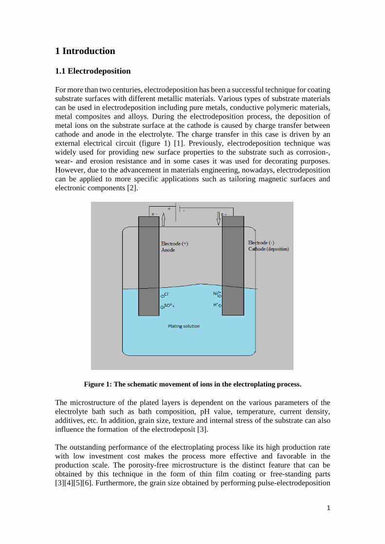
For more than two centuries, electrodeposition has been a successful technique for coating
substrate surfaces with different metallic materials. Various types of substrate materials
can be used in electrodeposition including pure metals, conductive polymeric materials,
metal composites and alloys. During the electrodeposition process, the deposition of
metal ions on the substrate surface at the cathode is caused by charge transfer between
cathode and anode in the electrolyte. The charge transfer in this case is driven by an
external electrical circuit (figure 1) [1]. Previously, electrodeposition technique was
widely used for providing new surface properties to the substrate such as corrosion-,
wear- and erosion resistance and in some cases it was used for decorating purposes.
However, due to the advancement in materials engineering, nowadays, electrodeposition
can be applied to more specific applications such as tailoring magnetic surfaces and
electronic components [2].
Figure 1: The schematic movement of ions in the electroplating process.
The microstructure of the plated layers is dependent on the various parameters of the
electrolyte bath such as bath composition, pH value, temperature, current density,
additives, etc. In addition, grain size, texture and internal stress of the substrate can also
influence the formation of the electrodeposit [3].
The outstanding performance of the electroplating process like its high production rate
with low investment cost makes the process more effective and favorable in the
production scale. The porosity-free microstructure is the distinct feature that can be
obtained by this technique in the form of thin film coating or free-standing parts
[3][4][5][6]. Furthermore, the grain size obtained by performing pulse-electrodeposition
2
can be below 10 nm. As a result, several properties can be influenced by this change of
grain size into nanoscale.
1.2 Electrodeposited Nanocrystalline Structure
Nanostructured material was first introduced by Gleiter [7] as the structure that is formed
in non-equilibrium state. When the grains are getting smaller than 100 nm, hardness and
wear resistance are increasing due to the large amount of grain boundaries and triple
junctions comprising the intercrystalline region. The increase in hardness and yield
strength in nanomaterials is in accordance with the Hall-Petch relationship. This behavior
is valid down to about 10 nm (depending on material) where an apparent softening occurs
which is described by the inverse Hall-Petch relationship. At these small grain sizes,
other deformation mechanisms set in [2][4][8]. However, there are also some properties
that show no or only a slight dependence on grain size such as Young’s modulus, thermal
expansion, heat capacity and saturation magnetization [2][8].
Different techniques can be utilized to synthesis nanostructure materials such as sol gel
technique, spark erosion, gas condensation, ball-milling and electroplating technique. In
the case of electroplating, the nanostructure of as-deposited materials can be obtained by
using pulse current instead of direct current [6]. Pulse-electroplating is one of the most
attractive techniques due to the distinctive structures obtained by the electrochemical
process and the outstanding properties of the nanostructure. The various parameters that
influence the nanostructures produced by electroplating technique are now more in the
research objective for better understanding in the way how each parameter is involved in
the formation mechanism of the nanocrystalline structure [8].
Crystallization of materials occurs with the competition between the nucleation of new
grains and the growth of the existing grains. The dominance of either nucleation or growth
process is dependent on the processing conditions. In electrodeposition, the nucleation
rate can be increased in the condition of high current density (overpotential) and low
surface diffusion of ad-atoms of existing grains which results in the achievement of
nanostructure. On the other hand, grain growth can occur in the condition of low current
density (overpotential) and high surface diffusion [2][3].
Generally, the microstructure produced by electrodeposition is influenced by the bath
conditions. However, in the very first layer of the deposited film, epitaxial grains can be
found which are influenced by the crystallographic structure of the substrate rather than
the bath conditions. This layer is formed for only a few microns. When the film layer
becomes thicker, the grains will grow in a preferred orientation depending on the bath
conditions [9][10].
1.3 Texture in Nickel Electrodeposition
According to Amblard et al. [10], two important theories have been used to describe the
anisotropy of the texture of Nickel electrodeposit which are explained from the opposite
viewpoints. One theory says that the competition in nucleation is responsible for the
anisotropy while the theory one suggests that it is the competitive growth that determines
the anisotropy. However, the literature data have shown that both theories are insufficient
to fully describe all experimental results.
3
Pangarov [9] suggested that the anisotropy of the texture of Nickel electrodeposit is
dependent on the nucleation process which is related to the overpotential. As mentioned
by Pangarov, the possible textures of the metals with fcc structure when increasing
overpotential are <111>-<100>-<110>-<311>-<210> [9]. However, this theory can be
explained only in the pure condition which means that neither the influence of defects on
the substrate surface nor the adsorption of other species in the electrolyte is considered.
However, in reality, metallic surfaces are usually not defect-free. Additionally, for the
transition materials with high surface energy such as Nickel, it is less likely that it does
not contain any adsorbed species. This means, the conditions are then considered to be
unrealistic [10].
Opposite to Pangarov’s theory, other authors state that the anisotropic texture of the
Nickel electrodeposit is determined by the growth process. In this way, the hydrogen
adsorption (Hads) becomes an important factor for controlling the texture during
electrodeposition. When the level of Hads increases, the texture develops from <110> to
<100> and finally <200>. Although this theory includes the consideration of the Hads
influence on the film texture, it is insufficient to explain all the possible preferred
orientations of the Nickel electrodeposit. This is due to the fact that Hads is not the only
species in the electrolyte that could inhibit the growth of the Nickel crystals [10][11].
In an additive-free bath, the <110>-texture is the inhibition growth mode influenced by
Hads while the <211>-texture is the result of the presence of Ni(OH)2. Also, <210>-texture
is affected by Hydrogen gas in the electrolyte. The growth of the <100>-texture cannot
be related to any inhibiting species and this is why this texture is considered as the free
growth mode. Each type of species can be linked to the pH value of the electrolyte. Hence,
the presence of a texture at a specific pH value and current density can be predicted as in
the diagram presented by Amblard et al. [10].
In pulse-electrodeposition, the adsorption and desorption of inhibitors on the substrate
surface can be hindered by the Ton- (plating time) and Toff-time (relaxation time) which
provide the possibility of creating deposit with better properties [12]. Molecular inhibitors
will desorb from the substrate surface during the relaxation period (Toff) while Hads and
anions behave contrarily, i.e. they will adsorb to the interface and inhibit the growth of
the Nickel coating on the surface. The perturbation that is dependent on the frequency
and duty cycle of the electroplating system plays an important role in determining the
characteristics of the Nickel electrodeposit. A small perturbation level provides less
structural defects with larger grain size, while at high perturbation, <110> growth mode
is dominant for all kinds of inhibiting species. This is due to the inhibition of Hads which
becomes the only factor governing the growth of the Nickel electrodeposit [12].
1.4 Microstructure in Nickel Electrodeposition
1.4.1 Epitaxial Region
The epitaxial layer is a very fine-grained layer formed next to the substrate surface with
the same structure and grain orientation as the substrate material. The main advantage of
this layer is to reduce the interfacial energy between the substrate and the electrodeposited
layer. The difference in lattice constants between substrate and deposited materials results
in the occurrence of a misfit strain in the epitaxial layer. This leads to a high dislocation
density in order to accommodate the misfit strain. A tolerable strain supported by the
4
microstructure can be up to 12%. Experimental results of the previous literature showed
that the thickness of the epitaxial layer of electrodeposited Nickel on a Cu substrate can
reach up to 100 nm before the columnar grains with no orientation relationship to the
substrate are formed [13].
1.4.2 Influence of Electroplating Parameters on Grain Size
The various parameters involved in the Nickel electrodeposition have been studied for
revealing the relation with the microstructure in order to improve the process of
synthesizing nanostructured Nickel [6][14][15][16][17][18]. Although the nanostructured
Nickel have already been produced, the tailoring of Nickel electrodeposit properties is
still complex. This is due to the uncertain results when the effects of all plating parameters
are involved.
Compared with the direct current (DC) electroplating [19][20], the on-time and off-time
intervals in pulse-electroplating have a significant influence on the microstructure of the
Nickel electrodeposit. The longer on-time and higher current density is applied, the
smaller grain size down to a few nanometers can be produced. The higher number of duty
cycle initiate more nucleation sites for Nickel crystals on the substrate and leads to the
smaller grain size. According to Ravi et al. [20], the grain size linearly decreases with the
higher number of duty cycle.
For the influence of current density on the grain size, the results are still controversial in
different studies. According to Rashidi [21], in pulse-electroplating process, the grain size
can be decreased with an increase in current density but the effect is just substantial up to
7.5 A/dm2. After that, a further increase in the current density will not influence the grain
refinement to the same extent. This finding is in contrast to some experiments
[14][15][18] on DC electroplating of Nickel where the grain size linearly increases with
increasing the current density.
The effect of temperature on the grain morphology is still not generally identified.
However, it is accepted that the deposition rate, coating quality and some other properties
can be altered with only small variations in bath temperature [22]. From the results
proposed by Rashidi [21], the grain size of electrodeposits will increase when the bath
temperature increases. But this behavior is only valid for temperatures above 55 °C. This
observation is also in accordance with the diagram introduced by Dini [23] and the study
on nanocrystalline electrodeposits by Natter et al. [24].
Additionally, the grain size of the electrodeposited materials is also dependent on other
parameters such as the frequency and the concentration of bath additives like saccharin
which acts as a grain refiner.

5
2 Materials and Experimental Procedure
The experimental section of the current thesis work had three objectives: (1) Production
of materials with nanocrystalline microstructure by adjusting the process parameters. (2)
Characterization of the electrodeposited materials. (3) Deposition of a Nickel coating on
polymer fibers in a sandwich structure and investigation of the coating quality.
2.1 Pulse-Electroplating Equipment
All samples were produced in the pulse-electroplating equipment illustrated in figure 2.
The equipment contains the following parts:
1. Propeller
2. Plating bath of 2 liters
3. Heating device for warming the electrolyte to the required temperature
4. Pulse generator
5. Oscilloscope for reading the current parameters
a

6
Figure 2: Pulse-Electroplating equipment: a) Overview of the equipment, b) anode and
cathode, i.e. sample holder and basket with Nickel pellets, and c) set-up of cathode, anode
and propeller.
2.2 Substrate Material
2.2.1 Stainless Steel
As substrate material, a stainless steel plate of 30 mm * 60 mm * 1.5 mm was used. The
stainless steel had the advantage that the Nickel coating could be easily stripped off
afterwards.
No mechanical preparation of the substrate was required before the electrodeposition
process. However, a cleaning and degreasing operation was performed. The substrate was
rinsed both under tap water and by ethanol and afterwards blow-dried in order to avoid
stains.
After the electrodeposition process, the coated layers were removed from the sample
holder and cleaned. This means, the electrodeposited films were rinsed under distilled
water and subsequently by ethanol. To avoid stains, the coated samples were cleaned for
5 or 10 minutes in an ultrasonic bath containing ethanol and afterwards blow-dried.
2.2.2 Polyamide Fibers
A set of experiments was performed in order to investigate if a Nickel electrodeposit
could be applied to strengthen the Hybrix™ sandwich material produced by Lamera AB.
The material investigated consisted of stainless steel plates between which Polyamide 6.6
fibers were attached with help of an Epoxy adhesive. The cross section of the sandwich
material can be seen in figure 3. Since the Polyamide fibers are not conductive, Gold
sputtering was chosen to create a conductive layer on the fibers. The process was
performed using an Edwards Sputter Coater S150B where the process was carried out at
1 kV within five minutes.
b c
7
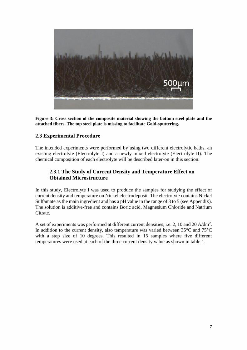
Figure 3: Cross section of the composite material showing the bottom steel plate and the
attached fibers. The top steel plate is missing to facilitate Gold-sputtering.
2.3 Experimental Procedure
The intended experiments were performed by using two different electrolytic baths, an
existing electrolyte (Electrolyte I) and a newly mixed electrolyte (Electrolyte II). The
chemical composition of each electrolyte will be described later-on in this section.
2.3.1 The Study of Current Density and Temperature Effect on
Obtained Microstructure
In this study, Electrolyte I was used to produce the samples for studying the effect of
current density and temperature on Nickel electrodeposit. The electrolyte contains Nickel
Sulfamate as the main ingredient and has a pH value in the range of 3 to 5 (see Appendix).
The solution is additive-free and contains Boric acid, Magnesium Chloride and Natrium
Citrate.
A set of experiments was performed at different current densities, i.e. 2, 10 and 20 A/dm2.
In addition to the current density, also temperature was varied between 35°C and 75°C
with a step size of 10 degrees. This resulted in 15 samples where five different
temperatures were used at each of the three current density value as shown in table 1.
8
Table 1: List of the conditions used for studying the current density and temperature effect
on Nickel electrodeposit.
Current Density (A/dm2) Temperature (°C)
2 35
45
55
65
75
10 35
45
55
65
75
20 35
45
55
65
75
2.3.2 The Study of Nickel Concentration and Current Density Effect
on the Obtained Microstructure
Electrolyte II was used to produce the samples for studying the effect of Nickel Sulfamate
concentration and current density on the formed microstructure. The electrolyte contains
a substantial amount of Nickel Sulfamate (Ni(SO3N2).4H2O) as the main source of Nickel
ions. In addition, Boric acid (H3BO3) and Magnesium Chloride were added. The solution
was continuously developed to investigate the influence of the Nickel Sulfamate
concentration on the appearance and microstructure of the electrodeposits. The initial
chemical composition of the electrolyte is stated in table 2 and the development of the
electrolyte is shown in table 3. Also, the conditions used for producing the samples are
displayed in table 4.
Table 2: The initial chemical composition of Electrolyte II showing the concentration of
Nickel Sulfamate in Molar [M].
Chemical Component
Nickel Sulfamate Ni(NH₂SO₃)₂
[M]
Boric Acid H₃BO₃
[g]
Magnesium Chloride MgCl₂
[g]
Sodium Citrate C6H5Na3O7
[g]
Water H₂O [L]
Amount 0.75 81.16 11.71 19.01 0.98
9
Table 3: The development of Nickel Sulfamate concentration in Electrolyte II.
Chemical
Component 1st
Concentration 2nd
Concentration 3rd
Concentration 4th
Concentration 5th
Concentration 6th
Concentration
Nickel Sulfamate
Ni(NH₂SO₃)₂ [M]
0.75 1.75 1.85 2.15 2.44 2.89
Table 4: List of the conditions used for studying the Nickel Sulfamate concentration and
current density effect on the formed microstructure.
Nickel Sulfamate Concentration (Molar)
Current Density (A/dm2)
1.85 2
10
20
2.15 2
10
20
2.44 2
10
20
2.89 2
10
20
2.4 Experimental Techniques
For investigation of the microstructure changes (i.e. grain size, texture, grain size
distribution, and surface topography) that take place when changing the process
parameters, different advanced characterization techniques were used.
2.4.1 X-Ray Diffraction
X-ray diffraction (XRD) is used to determine the interplanar spacing of crystalline
materials which provide information about the phase composition, residual stresses and
atomic structure. It also gives an impression about the overall texture when the
diffractogram is compared to that of a powder standard (which has a random texture and
is found in the database).
The working principle is based on a monochromatic X-ray beam which irradiates the
sample (under various angles ϴ) while the XRD detector is rotating and measures the
intensity of the diffracted beam as a function of 2ϴ (ϴ is the diffracted angle). The
information is collected, plotted and then compared to the data found in the database.
[25].
10
Investigations were performed by a Bruker D8 Advance X-ray diffractometer using a Cr-
anode (wavelength = 2.28970 Å) and a generator power of 35 kW and 40 mA. The angle
ϴ was varied in the range of 65⁰ to 140⁰. All samples were scanned at room temperature
for about 6 minutes each.
No sample preparation was required apart from that the samples were cut to a length of
40 mm in order to fit into the sample holder.
2.4.2 Scanning Electron Microscopy
In Scanning Electron Microscopy (SEM), an electron beam scans the sample surface and
as a result, various signals can be obtained such as backscattered electrons, secondary
electrons, and characteristic X-rays, which can be used for imaging and chemical analysis.
2.4.3 Electron Backscatter Diffraction
Electron Backscatter Diffraction (EBSD) is a technique that provides microstructural and
crystallographic information, e.g. local texture, grain morphology, grain boundary
distribution, grain size and grain size distribution [26]. The technique is able to inspect a
considerable amount of grains in a relatively short period of time. The EBSD detector is
an attachment to the SEM. With the cooperation of the required evaluation software, it
can be used to measure and identify electron backscattered diffraction patterns (EBSP or
Kikuchi patterns). To obtain so-called orientation map, a color-coded representation of
the grains in the microstructure, the sample is tilted 70° towards the EBSD detector in the
SEM and a defined area is scanned with a suitable step size (depending by the grain size).
At each point (pixel), an EBSP is captured with a CCD (Charge Coupled Device) camera
and the software indexes the obtained pattern by comparing it with the crystallographic
data of the expected phase which has to be selected before the investigation. A specific
color is addressed to the pixel which represents the measured orientation. In case that
indexing was not possible as a result of undefined phase, overlapping patterns from
adjacent grains or due to poor pattern quality, the pixel will be referred to as “zero
solution”.
In this thesis work, the samples were investigated using a Leo 1550 Gemini FEG-SEM
equipped with a Nordlys II EBSD detector and Channel 5 software by HKL Technologies.
Afterwards, the obtained data was analyzed further by Channel 5 software with respect
to grain size distribution in order to obtain pole figures and inverse pole figure diagrams.
Prior to EBSD analysis, the samples were prepared by electropolishing. A Struers
LectroPol-5 device with a Struers A2 electrolyte consisting of 70% Perchloric acid and
30% 2-Butoxyethanol was used for 10 seconds at a voltage of 31 V. The size of the
electropolished samples was around 1 cm. After electropolishing, the samples were rinsed
with Ethanol and placed in water for ending the corrosion process before they were blow-
dried.

11
3 Results
3.1 Surface Characterization
3.1.1 Effect of Temperature and Current Density on As-Deposited
Nickel Films
Based on the experiments, all the produced samples show a bright or semi-bright surface
where the degree of brightness differs in each sample depending on the plating condition.
In the temperature range between 55°C to 75°C, the as-plated Nickel films tend to have
duller surface when the current densities decrease. However, when produced at 35°C, the
films are shinier when the current density is decreased. In the case of a bath temperature
of 45°C, the sample with the best appearance was produced at 10 A/dm2. In general, at
all current densities, the Nickel coatings tend to become duller when the bath temperature
is decreased except for the sample produced at 35°C with 2 A/dm2 current density that
shows a really bright-shiny surface.
Waviness on the surface can be found in the samples produced at low plating temperature.
However, the waviness disappears when the current density is decreased (figure 5).
Pitting is another defect that can be observed in this study (figure 6). It is usually found
at moderate plating temperatures and its size is smaller when the current density
decreases. The thickness of the film obviously varies with the current density. When using
the same deposition time, the film thickness increases with the increase in current density.
The appearance of the produced samples is summarized in table 5 and 6.
Table 5: The effect of current density and temperature on the apperance of Nickel
electrodeposits.
Temperature
C urrent Density
35 ͦC 45 ͦC 55 ͦC 65 ͦC 75 ͦC
2 A/dm2
B
-
-
B
-
-
B
-
-
B
-
-
B
-
-
10 A/dm2
D
-
W
B
P
-
B
P
-
B
-
-
B
-
-
20 A/dm2
D
-
W
D
P
W
B
P
-
B
-
-
B
-
-
Description : 1st line------------> [Bright = B, Dull = D]
2nd line----------->[ Pitting = P]
3rd line------------>[Wavy = W]
12
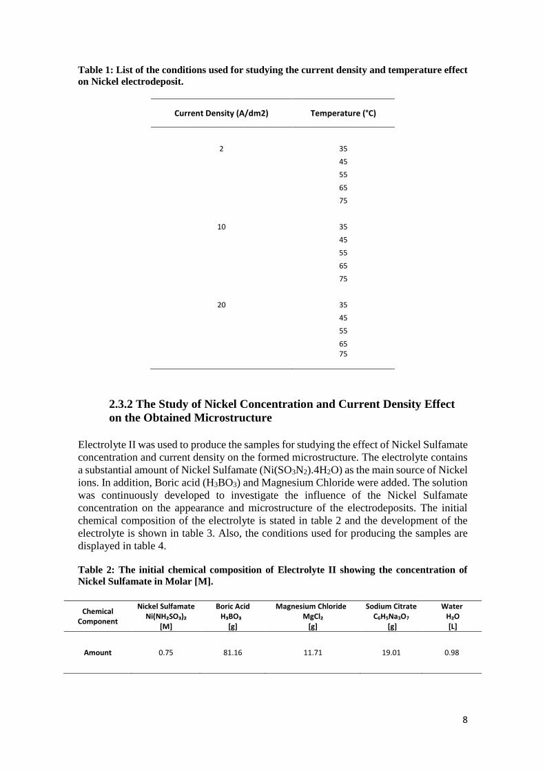
Table 6: The surface appearance of Nickel electrodeposits produced by varying current
density and temperature.
35° C 45 °C 55 °C 65 °C 75 °C
2 A/dm2
10 A/dm2
20 A/dm2
Figure 4: Bright and smooth surface of the sample produced at 20 A/dm2 and 65 °C.
Figure 5: Waviness of the sample produced at 20 A/dm2 and 35 °C.
Figure 6: Pitting observed in the sample produced at 20 A/dm2 and 45 °C.
Temperature Current
Density
13
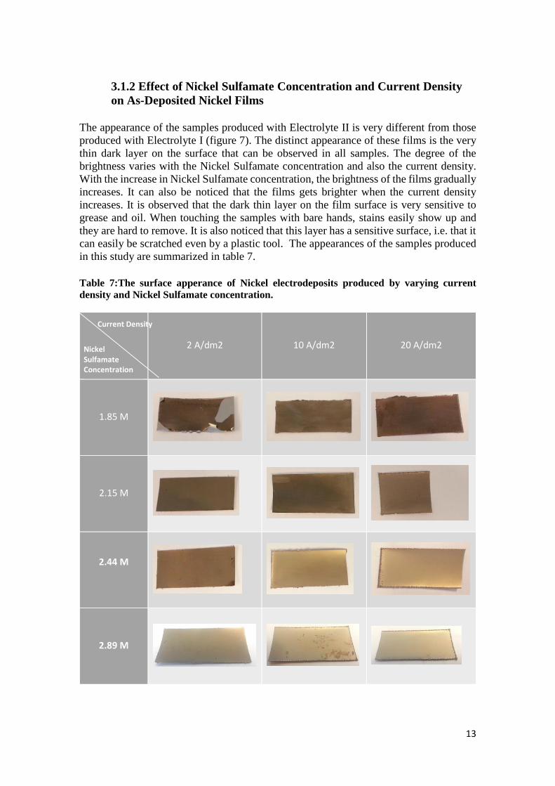
3.1.2 Effect of Nickel Sulfamate Concentration and Current Density
on As-Deposited Nickel Films
The appearance of the samples produced with Electrolyte II is very different from those
produced with Electrolyte I (figure 7). The distinct appearance of these films is the very
thin dark layer on the surface that can be observed in all samples. The degree of the
brightness varies with the Nickel Sulfamate concentration and also the current density.
With the increase in Nickel Sulfamate concentration, the brightness of the films gradually
increases. It can also be noticed that the films gets brighter when the current density
increases. It is observed that the dark thin layer on the film surface is very sensitive to
grease and oil. When touching the samples with bare hands, stains easily show up and
they are hard to remove. It is also noticed that this layer has a sensitive surface, i.e. that it
can easily be scratched even by a plastic tool. The appearances of the samples produced
in this study are summarized in table 7.
Table 7:The surface apperance of Nickel electrodeposits produced by varying current
density and Nickel Sulfamate concentration.
2 A/dm2 10 A/dm2 20 A/dm2
1.85 M
2.15 M
2.44 M
2.89 M
Current Density
Nickel Sulfamate Concentration
14
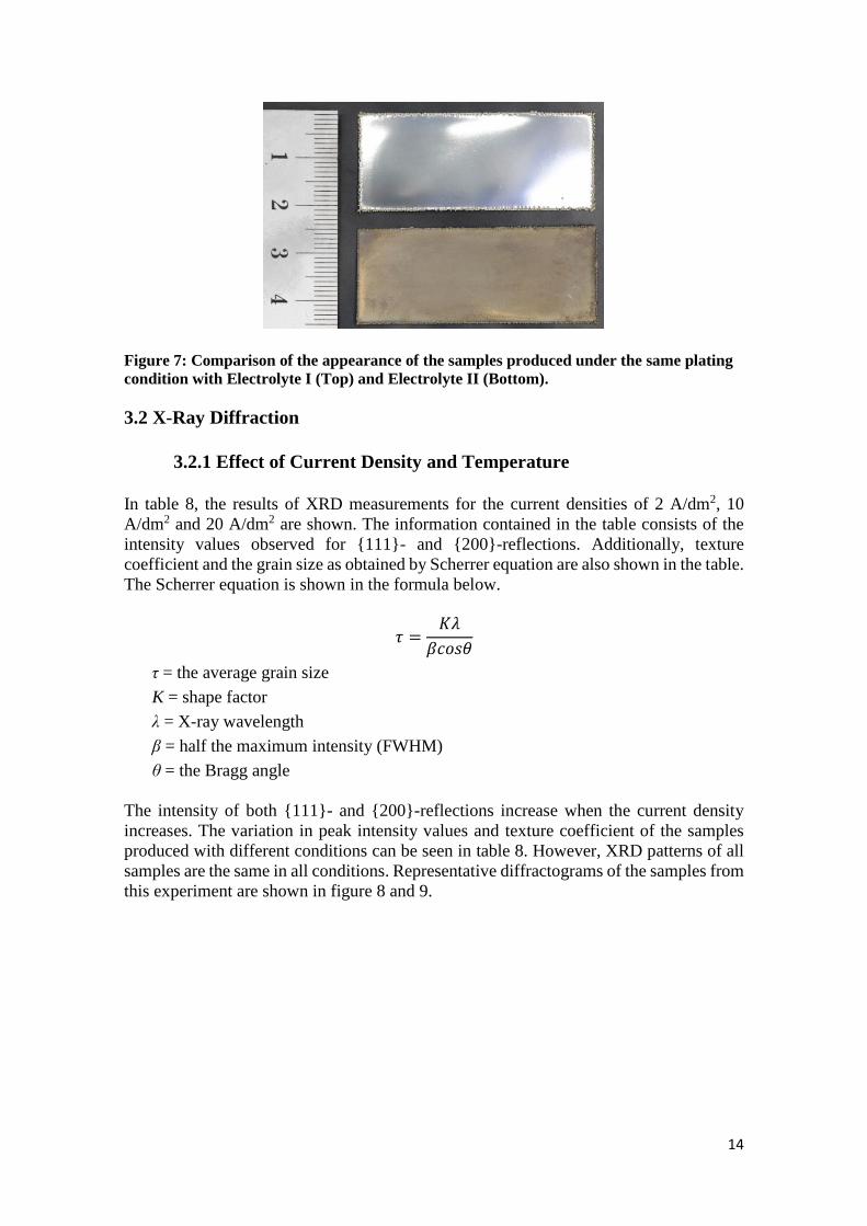
Figure 7: Comparison of the appearance of the samples produced under the same plating
condition with Electrolyte I (Top) and Electrolyte II (Bottom).
3.2 X-Ray Diffraction
3.2.1 Effect of Current Density and Temperature
In table 8, the results of XRD measurements for the current densities of 2 A/dm2, 10
A/dm2 and 20 A/dm2 are shown. The information contained in the table consists of the
intensity values observed for {111}- and {200}-reflections. Additionally, texture
coefficient and the grain size as obtained by Scherrer equation are also shown in the table.
The Scherrer equation is shown in the formula below.
𝜏 =𝐾𝜆
𝛽𝑐𝑜𝑠𝜃
τ = the average grain size
K = shape factor
λ = X-ray wavelength
β = half the maximum intensity (FWHM)
θ = the Bragg angle
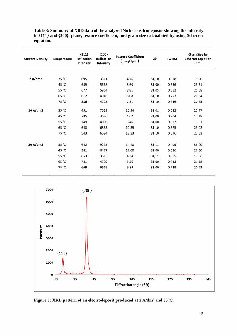
The intensity of both {111}- and {200}-reflections increase when the current density
increases. The variation in peak intensity values and texture coefficient of the samples
produced with different conditions can be seen in table 8. However, XRD patterns of all
samples are the same in all conditions. Representative diffractograms of the samples from
this experiment are shown in figure 8 and 9.
15
Table 8: Summary of XRD data of the analyzed Nickel electrodeposits showing the intensity
in {111} and {200} plane, texture coefficient, and grain size calcualated by using Scherrer
equation.
Current Density Temperature {111}
Reflection Intensity
{200} Reflection Intensity
Texture Coefficient ( I{200}/ I{111} )
2θ FWHM Grain Size by
Scherrer Equation (nm)
2 A/dm2 35 °C 695 3311 4,76 81,10 0,818 19,00
45 °C 659 5668 8,60 81,00 0,666 23,31
55 °C 677 5964 8,81 81,05 0,612 25,38
65 °C 612 4946 8,08 81,10 0,753 20,64
75 °C 586 4225 7,21 81,10 0,756 20,55
10 A/dm2 35 °C 451 7639 16,94 81,01 0,682 22,77
45 °C 785 3626 4,62 81,00 0,904 17,18
55 °C 749 4090 5,46 81,00 0,817 19,01
65 °C 648 6865 10,59 81,10 0,675 23,02
75 °C 543 6694 12,33 81,10 0,696 22,33
20 A/dm2 35 °C 642 9295 14,48 81,11 0,409 38,00
45 °C 381 6477 17,00 81,00 0,586 26,50
55 °C 853 3615 4,24 81,11 0,865 17,96
65 °C 781 4339 5,56 81,00 0,733 21,18
75 °C 669 6619 9,89 81,00 0,749 20,73
Figure 8: XRD pattern of an electrodeposit produced at 2 A/dm2 and 35°C.
{111}
{200}
16
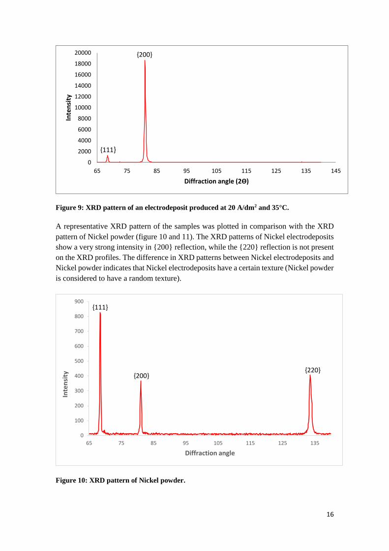
Figure 9: XRD pattern of an electrodeposit produced at 20 A/dm2 and 35°C.
A representative XRD pattern of the samples was plotted in comparison with the XRD
pattern of Nickel powder (figure 10 and 11). The XRD patterns of Nickel electrodeposits
show a very strong intensity in {200} reflection, while the {220} reflection is not present
on the XRD profiles. The difference in XRD patterns between Nickel electrodeposits and
Nickel powder indicates that Nickel electrodeposits have a certain texture (Nickel powder
is considered to have a random texture).
Figure 10: XRD pattern of Nickel powder.
0
2000
4000
6000
8000
10000
12000
14000
16000
18000
20000
65 75 85 95 105 115 125 135 145
Inte
nsi
ty
Diffraction angle (2ϴ)
{200}
0
100
200
300
400
500
600
700
800
900
65 75 85 95 105 115 125 135
Inte
nsi
ty
Diffraction angle
{111}
{200}{220}
{111}

17
Figure 11: Comparison of XRD patterns of as-deposited Nickel and Nickel powder.
3.2.2 Effect of Nickel Sulfamate Concentration and Current Density
Table 9 provides the XRD data collected from electrodeposits produced with Electrolyte
II. In addition to intensity values observed for {111} and {200} reflections, also data for
the {220} reflection are included. Additionally, texture coefficient and the grain size
obtained by Scherrer equation are provided in table 9. The schematic plots of two different
XRD patterns of the samples produced in this study are exhibited in figure 12 and 13. The
samples produced at 2 A/dm2 show a higher value of {111} peak intensity while the
samples produced at 20 A/dm2 reveal a higher {220} peak.
Figure 12: XRD profile of the sample produced at 2 A/dm2 and 2.44 M of Nickel Sulfamate
concentration showing the highest intensity in the {111} peak.
0
500
1000
1500
2000
2500
65 75 85 95 105 115 125 135 145
Inte
nsi
ty
Diffraction angle (2ϴ)
{111}
{200}
{220}
{111}
{200}
{220}
18
Figure 13: XRD profile of the sample produced at 20 A/dm2 and 2.44 M of Nickel Sulfamate
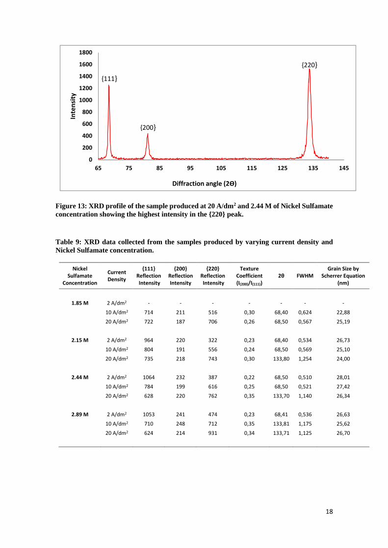
concentration showing the highest intensity in the {220} peak.
Table 9: XRD data collected from the samples produced by varying current density and
Nickel Sulfamate concentration.
Nickel Sulfamate
Concentration
Current Density
{111} Reflection Intensity
{200} Reflection Intensity
{220} Reflection Intensity
Texture Coefficient (I(200)/I(111))
2θ FWHM Grain Size by
Scherrer Equation (nm)
1.85 M 2 A/dm2 - - - - - - -
10 A/dm2 714 211 516 0,30 68,40 0,624 22,88
20 A/dm2 722 187 706 0,26 68,50 0,567 25,19
2.15 M 2 A/dm2 964 220 322 0,23 68,40 0,534 26,73
10 A/dm2 804 191 556 0,24 68,50 0,569 25,10
20 A/dm2 735 218 743 0,30 133,80 1,254 24,00
2.44 M 2 A/dm2 1064 232 387 0,22 68,50 0,510 28,01
10 A/dm2 784 199 616 0,25 68,50 0,521 27,42
20 A/dm2 628 220 762 0,35 133,70 1,140 26,34
2.89 M 2 A/dm2 1053 241 474 0,23 68,41 0,536 26,63
10 A/dm2 710 248 712 0,35 133,81 1,175 25,62
20 A/dm2 624 214 931 0,34 133,71 1,125 26,70
0
200
400
600
800
1000
1200
1400
1600
1800
65 75 85 95 105 115 125 135 145
Inte
nsi
ty
Diffraction angle (2ϴ)
{111}
{200}
{220}
19
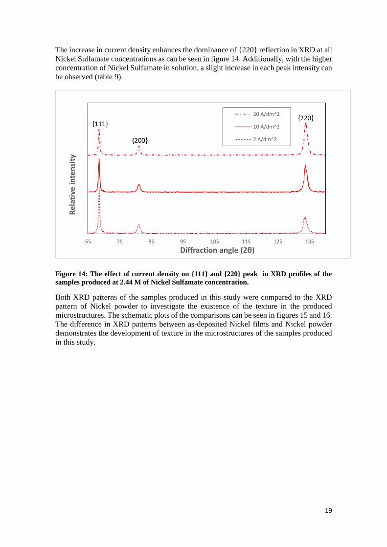
The increase in current density enhances the dominance of {220} reflection in XRD at all
Nickel Sulfamate concentrations as can be seen in figure 14. Additionally, with the higher
concentration of Nickel Sulfamate in solution, a slight increase in each peak intensity can
be observed (table 9).
Figure 14: The effect of current density on {111} and {220} peak in XRD profiles of the
samples produced at 2.44 M of Nickel Sulfamate concentration.
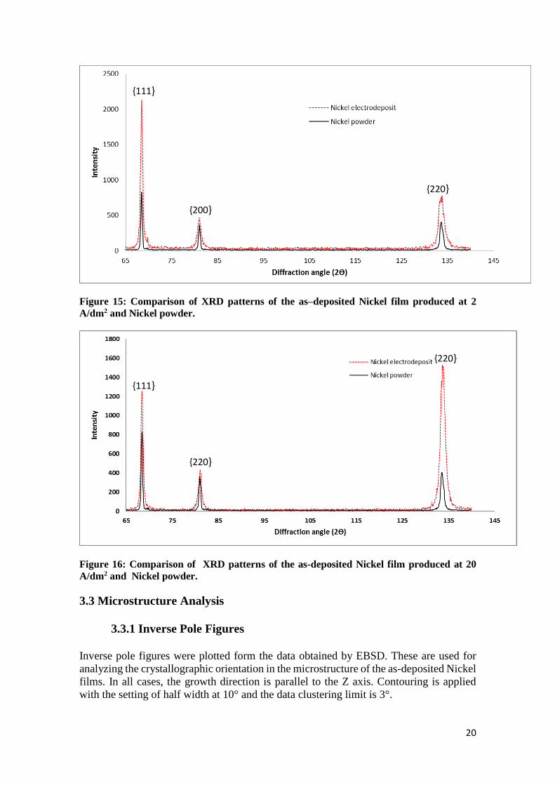
Both XRD patterns of the samples produced in this study were compared to the XRD
pattern of Nickel powder to investigate the existence of the texture in the produced
microstructures. The schematic plots of the comparisons can be seen in figures 15 and 16.
The difference in XRD patterns between as-deposited Nickel films and Nickel powder
demonstrates the development of texture in the microstructures of the samples produced
in this study.
65 75 85 95 105 115 125 135
Rel
ativ
e in
ten
sity
Diffraction angle (2θ)
20 A/dm^2
10 A/dm^2
2 A/dm^2{200}
{111} {220}
20
Figure 15: Comparison of XRD patterns of the as–deposited Nickel film produced at 2
A/dm2 and Nickel powder.
Figure 16: Comparison of XRD patterns of the as-deposited Nickel film produced at 20
A/dm2 and Nickel powder.
3.3 Microstructure Analysis
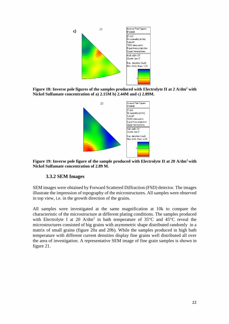
3.3.1 Inverse Pole Figures
Inverse pole figures were plotted form the data obtained by EBSD. These are used for
analyzing the crystallographic orientation in the microstructure of the as-deposited Nickel
films. In all cases, the growth direction is parallel to the Z axis. Contouring is applied
with the setting of half width at 10° and the data clustering limit is 3°.
{220}
{111}
{220}
{111}
{200}
{220}
21
Regarding the information of the samples produced with Electrolyte I, texture is not
influenced by the change in temperature and current density. All the as-prepared samples
show a strong preferred orientation of <100> in the growth direction. A representative
inverse pole figure of the samples is shown in figure 17.
Figure 17: Inverse pole figure of sample being representative for all samples produced with
Electrolyte I.
The samples produced with Electrolyte II at 2 A/dm2 with different Nickel Sulfamate
concentrations show a random texture (figure 18). In contrast, as-deposited Nickel films
produced at 20 A/dm2 with different Nickel Sulfamate concentrations show a weak
<110>-texture parallel to the growth direction (figure 19).
a)
b)
22
Figure 18: Inverse pole figures of the samples produced with Electrolyte II at 2 A/dm2 with
Nickel Sulfamate concentration of a) 2.15M b) 2.44M and c) 2.89M.
Figure 19: Inverse pole figure of the sample produced with Electrolyte II at 20 A/dm2 with
Nickel Sulfamate concentration of 2.89 M.
3.3.2 SEM Images
SEM images were obtained by Forward Scattered Diffraction (FSD) detector. The images
illustrate the impression of topography of the microstructures. All samples were observed
in top view, i.e. in the growth direction of the grains.
All samples were investigated at the same magnification at 10k to compare the
characteristic of the microstructure at different plating conditions. The samples produced
with Electrolyte I at 20 A/dm2 in bath temperature of 35°C and 45°C reveal the
microstructures consisted of big grains with asymmetric shape distributed randomly in a
matrix of small grains (figure 20a and 20b). While the samples produced in high bath
temperature with different current densities display fine grains well distributed all over
the area of investigation. A representative SEM image of fine grain samples is shown in
figure 21.
c)
23
Figure 20: SEM images of samples produced with Electrolyte I at 20 A/dm2 and a bath
temperature of a) 35°C and b) 45°C.
Figure 21: SEM image of sample produced with Electrolyte I at 20 A/dm2 and a bath
temperature of 55°C.
a
b
24
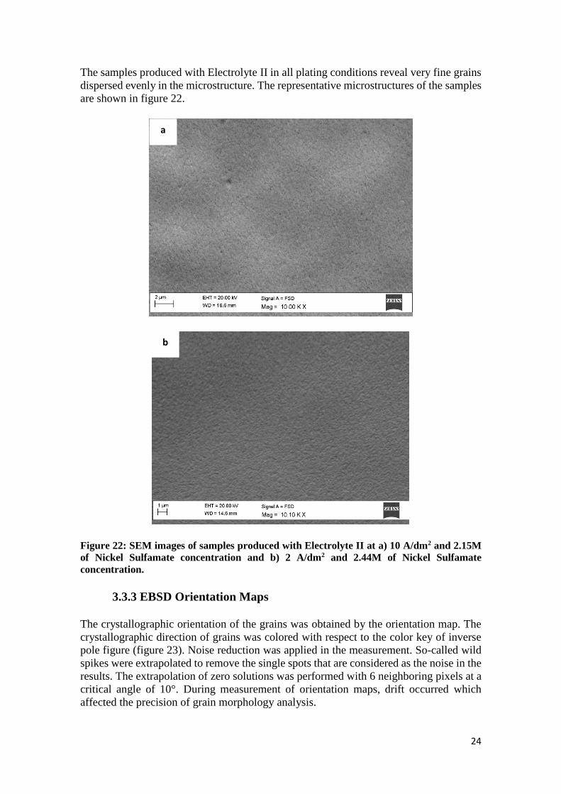
The samples produced with Electrolyte II in all plating conditions reveal very fine grains
dispersed evenly in the microstructure. The representative microstructures of the samples
are shown in figure 22.
Figure 22: SEM images of samples produced with Electrolyte II at a) 10 A/dm2 and 2.15M
of Nickel Sulfamate concentration and b) 2 A/dm2 and 2.44M of Nickel Sulfamate
concentration.
3.3.3 EBSD Orientation Maps
The crystallographic orientation of the grains was obtained by the orientation map. The
crystallographic direction of grains was colored with respect to the color key of inverse
pole figure (figure 23). Noise reduction was applied in the measurement. So-called wild
spikes were extrapolated to remove the single spots that are considered as the noise in the
results. The extrapolation of zero solutions was performed with 6 neighboring pixels at a
critical angle of 10°. During measurement of orientation maps, drift occurred which
affected the precision of grain morphology analysis.
b
a

25
Only the orientation maps of the normal direction (Z-axis parallel to the growth direction)
are shown. All samples produced with Electrolyte I show a very strong texture in <100>
but a different grain morphology. The samples produced at 20 A/dm2 with bath
temperature of 35°C and 45°C, respectively, reveal coarse grain structure (figure 24). The
microstructures of samples produced with Electrolyte I at high temperature with all
current densities show a combination of fine and coarse grains distributed evenly in the
investigated area (figure 25). However, a high fraction of zero solution (which most likely
is due to the small grain size) can be observed in these samples (see Appendix).
Figure 23: Color key for crystallographic orientations in inverse pole figure.
Figure 24: Orientation map of as-deposited Nickel film produced with Electrolyte I at 20
A/dm2 and 45°C.
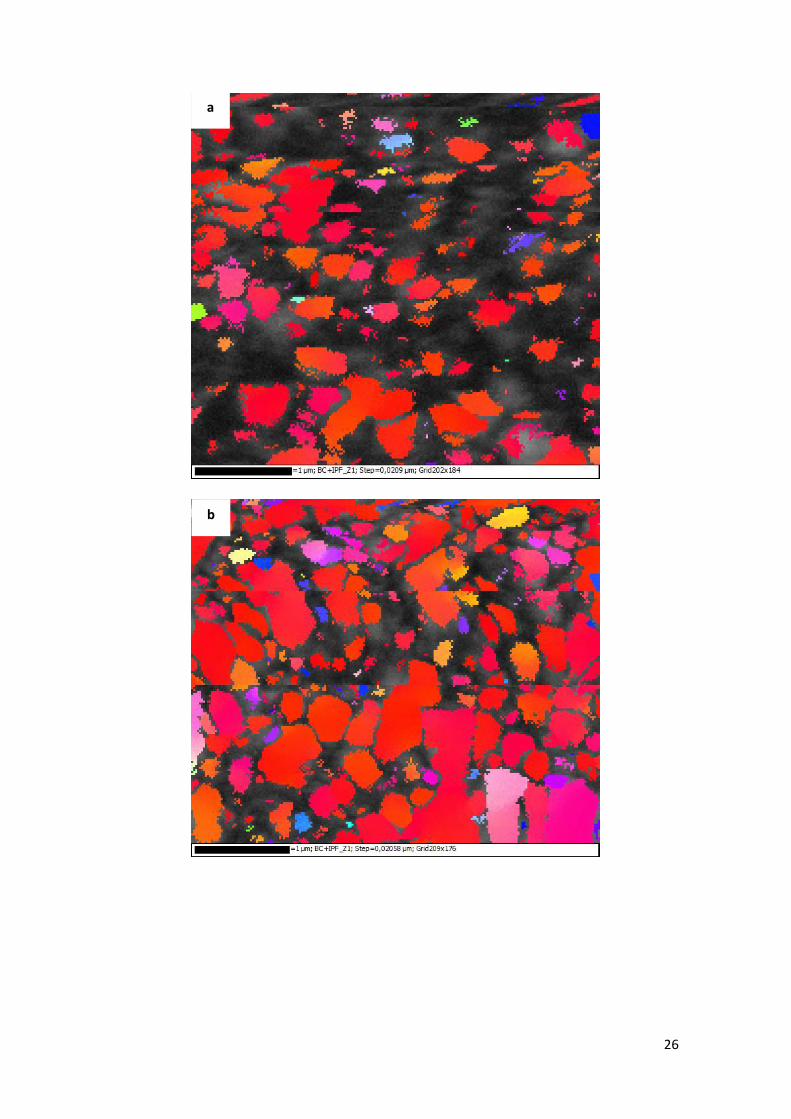
26
b
a
27
Figure 25: Orientation maps of as-deposited Nickel films produced with Electrolyte I at a)
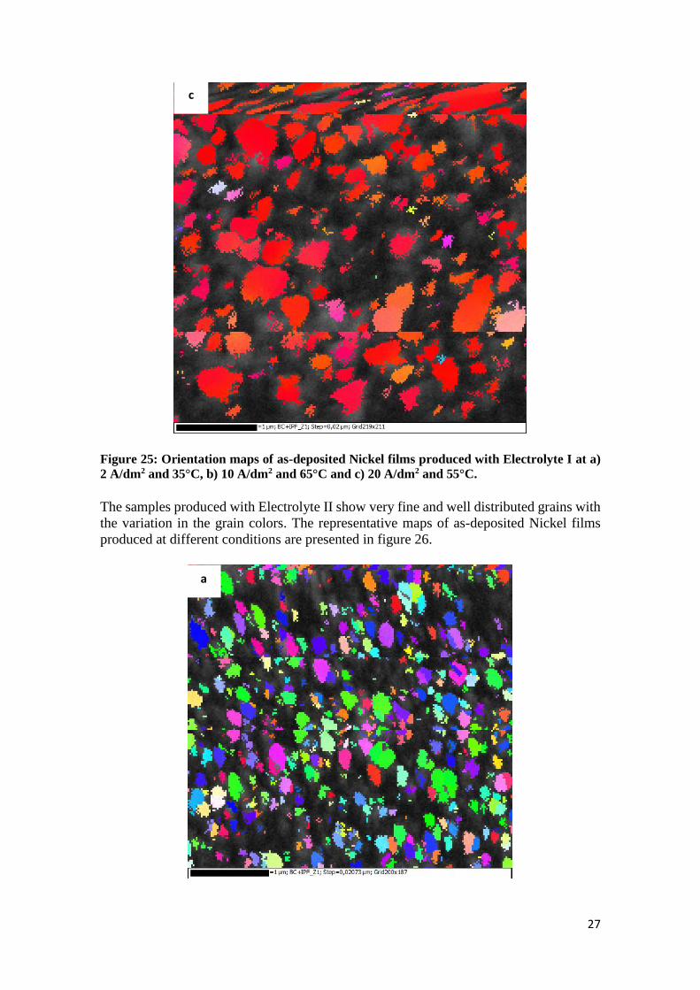
2 A/dm2 and 35°C, b) 10 A/dm2 and 65°C and c) 20 A/dm2 and 55°C.
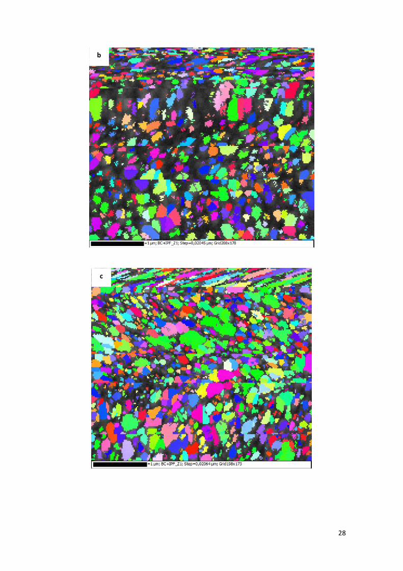
The samples produced with Electrolyte II show very fine and well distributed grains with
the variation in the grain colors. The representative maps of as-deposited Nickel films
produced at different conditions are presented in figure 26.
c
a
28
c
b

29
Figure 26: Orientation maps of as-deposited Nickel films produced with Electrolyte II at a)
2.15M and 2 A/dm2, b) 2.44M and 2 A/dm2, c) 2.89M and 2 A/dm2, and d) 2.89M and 20
A/dm2.
3.3.4 Grain Size Determination
Log-normal distribution histograms of the samples were plotted from the detected grains
found in the orientation maps. The critical misorientation angle was set to 10°. In the
present work, the consideration of grain boundary region and zero solution area were
excluded. Also the drifting area which affect to the precision of the grain size calculation
was excluded.
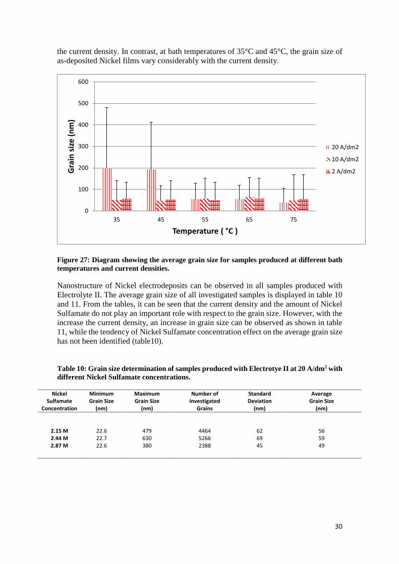
The analysis of the grain size of the samples produced with Electrolyte I at different bath
temperatures and current densities is summarized as a bar chart in figure 27 (see Appendix
for all data). The average grain sizes of the Nickel electrodeposits produced at 20 A/dm2
at a bath temperature of 35°C and 45°C are 200±281 nm and 193±219 nm, respectively.
The average grain size of 39±66 nm was the lowest average grain size found in the sample
produced at 75°C. When prepared at temperature of 55°C and 65°C, Nickel
electrodeposits reveal a slightly larger average grain size than the samples produced at
75°C.
In contrast to the sample produced at 20 A/dm2, the samples produced at 2 A/dm2 and 10
A/dm2 show an average grain size lower than 100 nm at all plating temperatures.
As can be seen from the experimental data, bath temperatures in the range of 55°C to
75°C are providing Nickel electrodeposits to which the grain size is less influenced by
d
30
the current density. In contrast, at bath temperatures of 35°C and 45°C, the grain size of
as-deposited Nickel films vary considerably with the current density.
Figure 27: Diagram showing the average grain size for samples produced at different bath
temperatures and current densities.
Nanostructure of Nickel electrodeposits can be observed in all samples produced with
Electrolyte II. The average grain size of all investigated samples is displayed in table 10
and 11. From the tables, it can be seen that the current density and the amount of Nickel
Sulfamate do not play an important role with respect to the grain size. However, with the
increase the current density, an increase in grain size can be observed as shown in table
11, while the tendency of Nickel Sulfamate concentration effect on the average grain size
has not been identified (table10).
Table 10: Grain size determination of samples produced with Electrotye II at 20 A/dm2 with
different Nickel Sulfamate concentrations.
Nickel Sulfamate
Concentration
Minimum Grain Size
(nm)
Maximum Grain Size
(nm)
Number of Investigated
Grains
Standard Deviation
(nm)
Average Grain Size
(nm)
2.15 M 22.6 479 4464
62 56 2.44 M 22.7 630 5266 69 59 2.87 M 22.6 380 2388 45 49
0
100
200
300
400
500
600
35 45 55 65 75
Gra
in s
ize
(nm
)
Temperature ( °C )
20 A/dm2
10 A/dm2
2 A/dm2
31
Table 11: Grain size determination of samples produced with Electrolyte II at 2.44 M of
Nickel Sulfamate concentration with different current densities.
Current Density
Minimum Grain Size
(nm)
Maximum Grain Size
(nm)
Number of Investigated
Grains
Standard Deviation
(nm)
Average Grain Size
(nm)
2 A/dm2 23 316 1873
40 48 10 A/dm2 24 328 2088 41 49 20 A/dm2 23 630 5266 69 59
3.4 Pulse-Electroplating on Sandwich Material
Due to their outstanding mechanical properties with low weight, sandwich materials are
starting to replace the conventional single-structure materials. To further improve their
mechanical properties, pulse-electroplating was chosen to strengthen the sandwich
material consisting of stainless steel plates to which Polyamide 6.6 fibers were attached.
Since the Polyamide fibers are not conductive, Gold sputtering was used to provide a
conductive coating on the fibers. As seen when using optical microscopy, the Gold
particles were deposited homogeneously on the fiber surface and covered the entire length
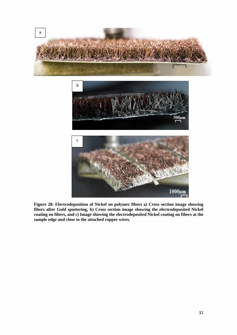
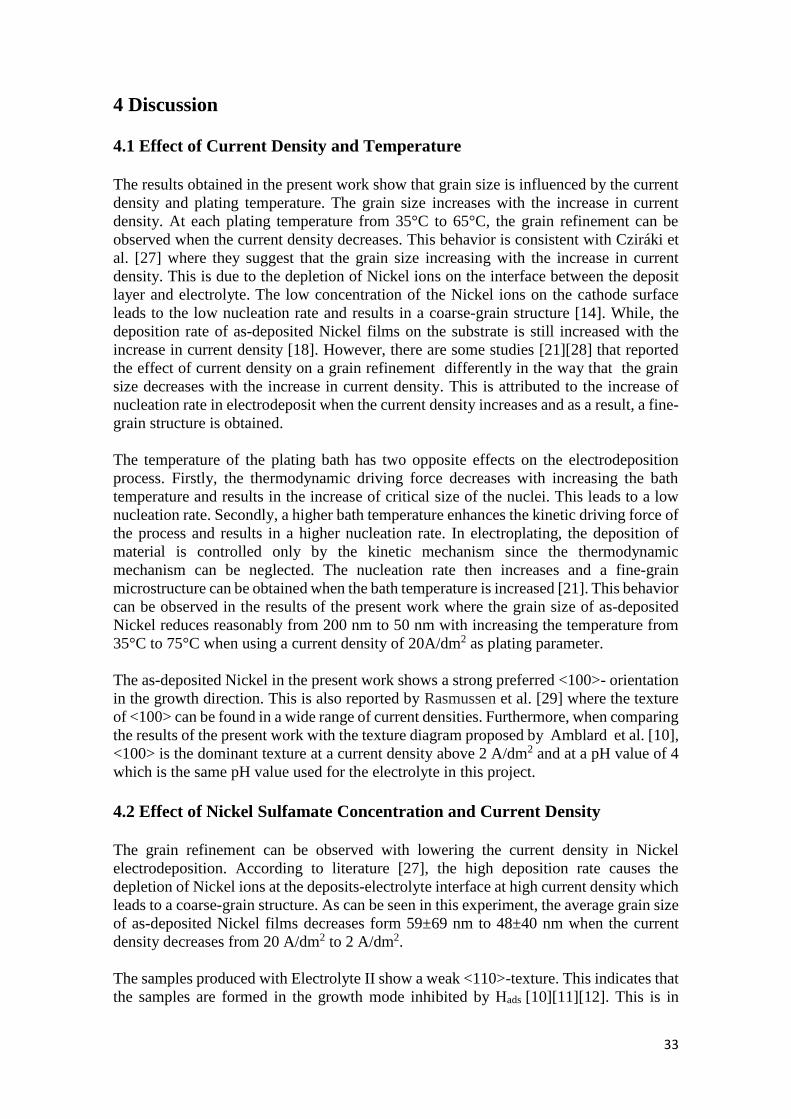
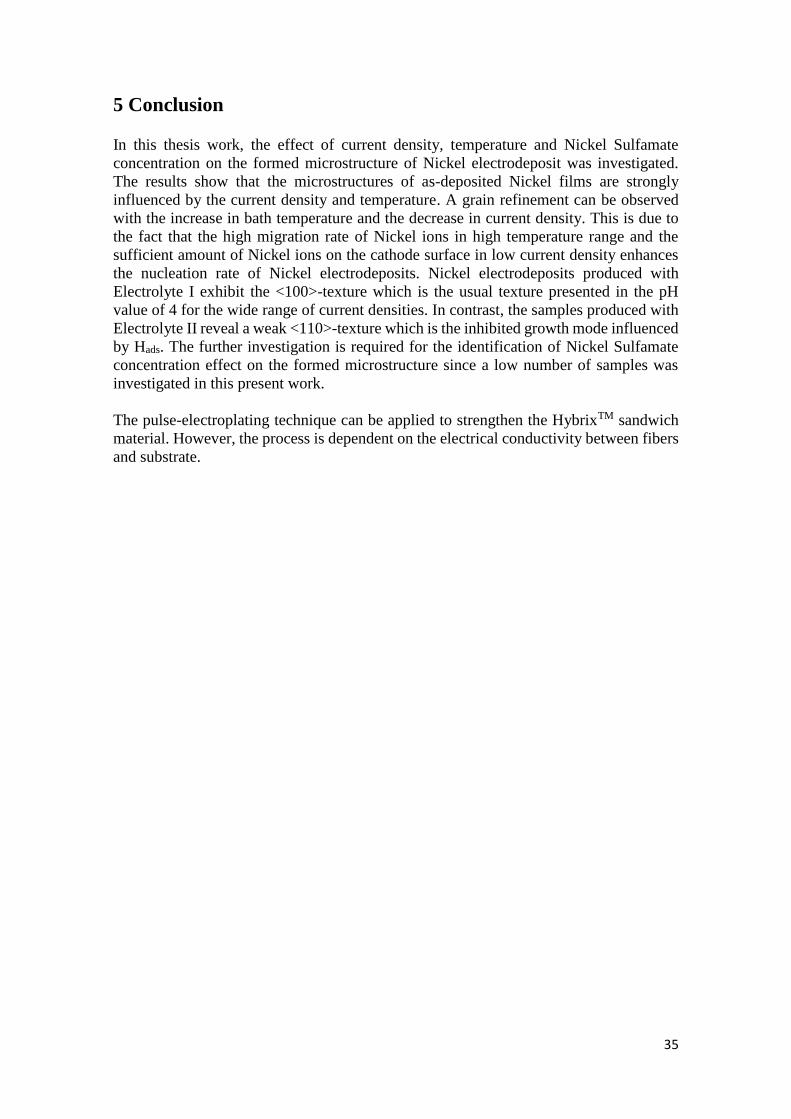
of the fibers down to the adhesive layer (figure 28a). After two-hour pulse-electroplating,
a Nickel electrodeposit could clearly be seen on the fibers situated on the sample edges
and in the area around the Copper wires which were attached to improve the conductivity
between the fibers and the substrate. Fibers in the middle of the sample and further away
from the Copper wires were not covered to the same extent (figure 28b and 28c) even
though a Gold layer was present on the fiber surface.
32
Figure 28: Electrodeposition of Nickel on polymer fibers a) Cross section image showing
fibers after Gold sputtering, b) Cross section image showing the electrodeposited Nickel
coating on fibers, and c) Image showing the electrodeposited Nickel coating on fibers at the
sample edge and close to the attached copper wires.
c
1000µm
b
a
33
4 Discussion
4.1 Effect of Current Density and Temperature
The results obtained in the present work show that grain size is influenced by the current
density and plating temperature. The grain size increases with the increase in current
density. At each plating temperature from 35°C to 65°C, the grain refinement can be
observed when the current density decreases. This behavior is consistent with Cziráki et
al. [27] where they suggest that the grain size increasing with the increase in current
density. This is due to the depletion of Nickel ions on the interface between the deposit
layer and electrolyte. The low concentration of the Nickel ions on the cathode surface
leads to the low nucleation rate and results in a coarse-grain structure [14]. While, the
deposition rate of as-deposited Nickel films on the substrate is still increased with the
increase in current density [18]. However, there are some studies [21][28] that reported
the effect of current density on a grain refinement differently in the way that the grain
size decreases with the increase in current density. This is attributed to the increase of
nucleation rate in electrodeposit when the current density increases and as a result, a fine-
grain structure is obtained.
The temperature of the plating bath has two opposite effects on the electrodeposition
process. Firstly, the thermodynamic driving force decreases with increasing the bath
temperature and results in the increase of critical size of the nuclei. This leads to a low
nucleation rate. Secondly, a higher bath temperature enhances the kinetic driving force of
the process and results in a higher nucleation rate. In electroplating, the deposition of
material is controlled only by the kinetic mechanism since the thermodynamic
mechanism can be neglected. The nucleation rate then increases and a fine-grain
microstructure can be obtained when the bath temperature is increased [21]. This behavior
can be observed in the results of the present work where the grain size of as-deposited
Nickel reduces reasonably from 200 nm to 50 nm with increasing the temperature from
35°C to 75°C when using a current density of 20A/dm2 as plating parameter.
The as-deposited Nickel in the present work shows a strong preferred <100>- orientation
in the growth direction. This is also reported by Rasmussen et al. [29] where the texture
of <100> can be found in a wide range of current densities. Furthermore, when comparing
the results of the present work with the texture diagram proposed by Amblard et al. [10],
<100> is the dominant texture at a current density above 2 A/dm2 and at a pH value of 4
which is the same pH value used for the electrolyte in this project.
4.2 Effect of Nickel Sulfamate Concentration and Current Density
The grain refinement can be observed with lowering the current density in Nickel
electrodeposition. According to literature [27], the high deposition rate causes the
depletion of Nickel ions at the deposits-electrolyte interface at high current density which
leads to a coarse-grain structure. As can be seen in this experiment, the average grain size
of as-deposited Nickel films decreases form 59±69 nm to 48±40 nm when the current
density decreases from 20 A/dm2 to 2 A/dm2.
The samples produced with Electrolyte II show a weak <110>-texture. This indicates that
the samples are formed in the growth mode inhibited by Hads [10][11][12]. This is in

34
accordance with the results from Klement et al. [30] where the samples produced in an
additive -free bath contain a weak <110>-texture parallel to the growth direction. The
same additive-free bath is used in this thesis work.
4.3 Pulse-Electroplating on Sandwich Material
After the electroplating process, the electrodeposited coating layer on the fibers was
investigated. Fibers situated at the edge of the sample and also a small region around the
Copper wires was covered by a Nickel electrodeposit. This result could be related to the
conductivity of material. The surface that was easily exposed to the Au-ions could
become more conductive than the region located in the center of the sample. In addition,
even if the fibers were Gold-sputtered but they were not connected to each other and to
the substrate, the pulse-electroplating process could not be achieved.
35
5 Conclusion In this thesis work, the effect of current density, temperature and Nickel Sulfamate
concentration on the formed microstructure of Nickel electrodeposit was investigated.
The results show that the microstructures of as-deposited Nickel films are strongly
influenced by the current density and temperature. A grain refinement can be observed
with the increase in bath temperature and the decrease in current density. This is due to
the fact that the high migration rate of Nickel ions in high temperature range and the
sufficient amount of Nickel ions on the cathode surface in low current density enhances
the nucleation rate of Nickel electrodeposits. Nickel electrodeposits produced with
Electrolyte I exhibit the <100>-texture which is the usual texture presented in the pH
value of 4 for the wide range of current densities. In contrast, the samples produced with
Electrolyte II reveal a weak <110>-texture which is the inhibited growth mode influenced
by Hads. The further investigation is required for the identification of Nickel Sulfamate
concentration effect on the formed microstructure since a low number of samples was
investigated in this present work.
The pulse-electroplating technique can be applied to strengthen the HybrixTM sandwich
material. However, the process is dependent on the electrical conductivity between fibers
and substrate.
36
Future Recommendations
1. In this project, the effect of the current density, temperature and Nickel Sulfamate
concentration have been investigated. Considering the wide number of the process
parameters that could affect the formed microstructure, the effect of parameters
such as pH value, duty cycle, distance between anode and cathode would be of
interest for further investigations. In addition, saccharin which acts as a grain
refiner could be added in the electrodeposition process and its effect could be
further investigated.
2. With regard to HybrixTM sandwich material, another set of pulse-electroplating
operations could be performed for another material where the present non-
conductive epoxy adhesive is replaced by a conductive adhesive. The replacement
will increase the conductivity between fibers and substrate and the pulse-
electroplating could provide better results.

37
Reference [1] M. Paunovic and M.Schlesinger, Modern electroplating, 5th ed. New Jersey: John
Wiley & Sons, Inc., 2011.
[2] U. Erb, K.T. Aust, G. Palumbo, “Electrodeposited nanocrystalline metals,
alloys and composites,” in Nanostructured materials – processing,
properties, and applications, C.C. Koch, Ed., 2nd ed. New York: William
Andrew, 2007, pp. 235-292.
[3] R. Abdel-Karim and A. F. Waheed, “Nanocoatings,” in Modern Surface
Engineering Treatments, A. Mahmood, Ed.:Intech, 2013.
[4] U. Erb and A.M. El-Sherik, “Nanocrystalline metals and process of producing the
same,” U.S. Patent 5 352 266, Oct 4, 1994.
[5] U. Erb, A.M. El-Sherik, G. Palumbo and K.T. Aust, “Synthesis, structure and
properties of electroplated nanocrystalline materials,” Nanostructured Mater., Vol.
2, no. 2, pp. 383–390, 1993.
[6] U. Erb and A.M. El-Sherik, “Synthesis of bulk nanocrystalline nickel by pulsed
electrodeposition,” J. Mater. Sci., Vol. 30, pp. 5743–5749, 1995.
[7] H. Gleiter, “Nanocrystalline Materials,” Prog. Mater. Sci., Vol. 33, pp. 223–315,
1990.
[8] U. Erb, “Electrodeposited nanocrystals: synthesis, properties and industrial
applications,” Nanostruct. Mater., Vol. 6, pp. 533–538, 1995.
[9] N.A. Pangarov, “Preferred orientations in electrodeposited metals,” J. Electroanal.
Chem., Vol. 9, pp. 70-85, 1965.
[10] J. Amblard and M. Froment, “New interpretation of texture formation in
nickel electrodeposits,” Faraday Symp. Chem. Soc., Vol. 12, pp. 136-144,
1977.
[11] J. Amblard, I. Epelboin, M. Froment, and G. Maurin, “Inhibition and nickel
electrocrystallization,” J. Appl. Electrochem., Vol. 9, no. 4, pp. 233–242, 1979.
[12] C. Kollia, N. Spyrellis, J. Amblard, M. Froment, and G. Maurin, “Nickel plating
by pulse electrolysis: textural and microstructural modifications due to
adsorption/desorption phenomena,” J. Appl. Electrochem., Vol. 20, pp. 1025–
1032, 1990.
[13] A. Shibata, H. Noda, M. Sone, and Y. Higo, “Microstructural development of an
electrodeposited Ni layer,” Thin Solid Films, Vol. 518, no. 18, pp. 5153–5158,
2010.
[14] I. Bakonyi, E. Tóth-Kádár, L. Pogány, Á. Cziráki, I. Gerőcs, K. Varga-Josepovits,
B. Arnold, and K. Wetzig, “Preparation and characterization of d.c.-plated
38
nanocrystalline nickel electrodeposits,” Surf. Coatings Technol., Vol. 78, no. 1–3,
pp. 124–136, 1996.
[15] I. Bakonyi, E. Tóth-Kádár, T. Tarnóczi, L. K. Varga, Á. Cziráki, I. Geröcs, and B.
Fogarassy, “Structure and properties of fine-grained electrodeposited nickel,”
Nanostructured Mater., Vol. 3, no. 1–6, pp. 155–161, 1993.
[16] Y. Xuetao, W. Yu, S. Dongbai, and Y. Hongying, “Influence of pulse parameters
on the microstructure and microhardness of nickel electrodeposits,” Surf. Coatings
Technol., Vol. 202, no. 9, pp. 1895–1903, 2008.
[17] R. T. C. Choo, J. M. Toguri, a. M. El-Sherik, and U. Erb, “Mass transfer and
electrocrystallization analyses of nanocrystalline nickel production by pulse
plating,” J. Appl. Electrochem., Vol. 25, no. 4, pp. 384–403, 1995.
[18] F. Ebrahimi and Z. Ahmed, “The effect of current density on properties of
electrodeposited nanocrystalline nickel,” pp. 733–739, 2003.
[19] A. M. El-Sherik, U. Erb, and J. Page, “Microstructural evolution in pulse plated
nickel electrodeposits,” Surf. Coatings Technol., Vol. 88, pp. 70–78, 1997.
[20] S. Ravi, K. V. Ganesh, A. Ramanathan, J. Annamalai, and P. K. Jaiswal,
“Development of Nanocrystalline Nickel Coating for Engineering Applications,”
Key Eng. Mater., Vol. 443, pp. 487–492, 2010.
[21] A. M. Rashidi and A. Amadeh, “Effect of electroplating parameters on
microstructure of nanocrystalline nickel coatings,” J. Mater. Sci. Technol., Vol.
26, no. 1, pp. 82–86, 2010.
[22] M. Paunovic and M. Schlesinger, Fundamentals of Electrochemical Deposition,
2nd ed. New Jersey: John Wiley & Sons, Inc., 2006.
[23] J.W. Dini, Electrodeposition - The Materials Science of Coatings and Substrates.
New Jersey: Noyes Publications, 1993
[24] H. Natter and R. Hempelmann, “Tailor-made nanomaterials designed by
electrochemical methods,” Electrochim. Acta, Vol. 49, no. 1, pp. 51–61, 2003.
[25] O. Engler, V. Randle, Introduction to Texture Analysis: Macrotexture,
Microtexture and Orientation Mapping, 2nd ed. Boca Ratan: CRC Press,
2010.
[26] Oxford Instrument Plc, “EBSD Electron Backscatter Diffraction Analysis,”
[Online]. Available: http://www.ebsd.com [Accessed: May. 4, 2015].
[27] Á. Cziráki, B.F. Fogarassy, I. Geröcs, E. Töth-Kádár, I. Bakonyi, J. Mater. Sci.,
Vol. 29, pp. 4771, 1994.
[28] P.Q. Dai, Hui Yu and Q. Li: Trans. Mater. Heat Treatment, Vol. 25, pp.
1283, 2004. (in Chinese)

39
[29] A.A. Rasmussen, P. Møller, M.A.J. Somers, “Microstructure and thermal stability
of nickel layers electrodeposited from an additive-free sulphamate based
electrolyte,” Surface and coating technology, Vol. 200, pp. 6037-6046, 2006.
[30] U. Klement, C. Oikonomou, R. Chulist, B. Beausir, L. Hollang, W. Skrotzki,
“Influence of Additives on Texture Development of Submicro- and
Nanocrystalline Nickel,” Materials Science Forum, Vols. 702-703, pp 928-931,
2012.
40
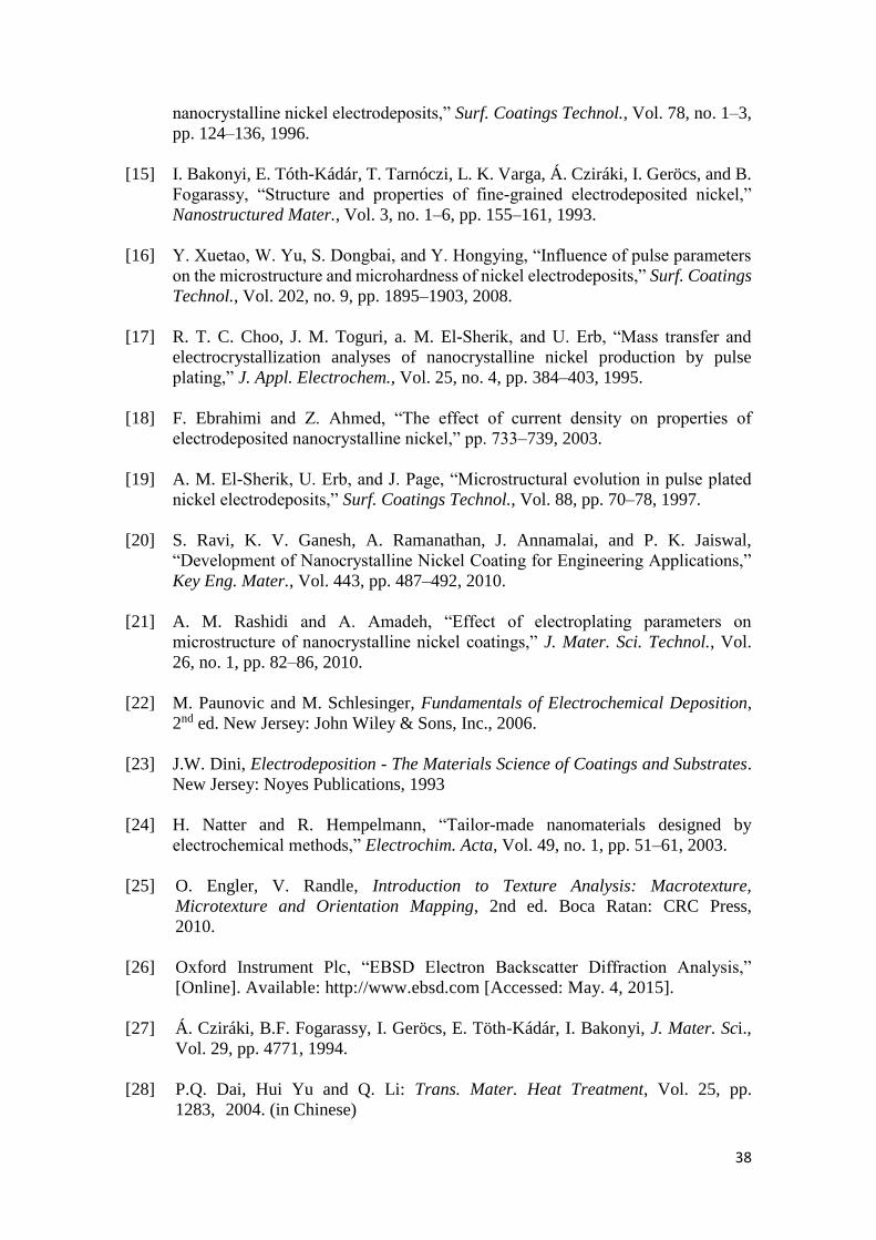
Appendix: Grain Size Determination In the following tables, the results from grain size determination of as-deposited Nickel
films produced with Electrolyte I and II are summarized. All the samples were
investigated by EBSD with the scanning step size of 0.02 µm, except the samples
produced at 2 A/dm2 with a bath temperature of 35°C and 45°C which were investigated
with the scanning step size of 0.07 µm.
Table 12: Summary of the results from the grain size determination of as-deposited Nickel
films produced with Electrolyte I by varying current density and temperature.
Current Density (A/dm2)
Temperature ( °C )
pH Value Number of
Investigated Grains
Zero solution Phase Fraction
(%)
Standard Deviation
(nm)
Average Grain Size
(nm)
2 35 3 528 70.96 77 57
45 3 505 63.58 87 54
55 4 462 57.35 85 49
65 4 812 50.40 91 60
75 4 417 51.11 113 55
10 35 4 502 65.89 90 51
45 4 436 80.71 69 47
55 4 483 60.37 94 58
65 3 582 43.43 91 64
75 4 371 47.87 120 49
20 35
2-3 1473 23.16 281 200
45 2-3 1761 20.46 219 193
55 2-3 739 69.42 73 55
65 2-3 744 49.77 64 55
75 3 483 76.61 66 39
Table 13: Summary of the results from the grain size determination of as-deposited Nickel
films produced with Electrolyte II by varying Nickel Sulfamate concentration and current
density.
Nickel Sulfamate Concentration
(M)
Current Density (A/dm2)
pH Value Number of
Investigated Grains
Zero Solution
phase Fraction (%)
Standard Deviation
(nm)
Average Grain Size
(nm)
2.15 2 4 1341 70.25 43 48
20 4 4464 66.27 62 56
2.44 2 4-5 1873 60.37 40 48
10 4 2088 51.16 41 49
20 4 5266 60.04 69 59
2.87 2 4 2693 39 47
20 4 2388 40.21 45 49

41