printed supercapacitors for energy harvesting applications · printed supercapacitors for energy...
TRANSCRIPT

Tampere University of Technology
Printed Supercapacitors for Energy Harvesting Applications
CitationLehtimäki, S. (2017). Printed Supercapacitors for Energy Harvesting Applications. (Tampere University ofTechnology. Publication; Vol. 1463). Tampere University of Technology.
Year2017
VersionPublisher's PDF (version of record)
Link to publicationTUTCRIS Portal (http://www.tut.fi/tutcris)
Take down policyIf you believe that this document breaches copyright, please contact [email protected], and we will remove access tothe work immediately and investigate your claim.
Download date:14.07.2018
Suvi LehtimäkiPrinted Supercapacitors for Energy Harvesting Applications
Julkaisu 1463 • Publication 1463
Tampere 2017
Tampereen teknillinen yliopisto. Julkaisu 1463 Tampere University of Technology. Publication 1463 Suvi Lehtimäki Printed Supercapacitors for Energy Harvesting Applications Thesis for the degree of Doctor of Science in Technology to be presented with due permission for public examination and criticism in Rakennustalo Building, Auditorium RG202, at Tampere University of Technology, on the 7th of April 2017, at 12 noon. Tampereen teknillinen yliopisto - Tampere University of Technology Tampere 2017

Doctoral candidate: Suvi Lehtimäki, M.Sc. Department of Electronics and Communications Engineering Tampere University of Technology Supervisors: Donald Lupo, Prof. Laboratory for Future Electronics Department of Electronics and Communications Engineering Tampere University of Technology Sampo Tuukkanen, Asst. Prof. Department of Automation Science and Engineering Tampere University of Technology Pre-examiners: Olli Ikkala, Prof. Department of Applied Physics Aalto University Li-Rong Zheng, Prof. School of Information and Communication Technology KTH Royal Institute of Technology Opponent: Leif Nyholm, Prof. Department of Chemistry Uppsala University Painopaikka: Juvenes Print Suomen Yliopistopaino Oy Tampere 2017 ISBN 978-952-15-3922-0 (printed) ISBN 978-952-15-3927-5 (PDF) ISSN 1459-2045
Abstract
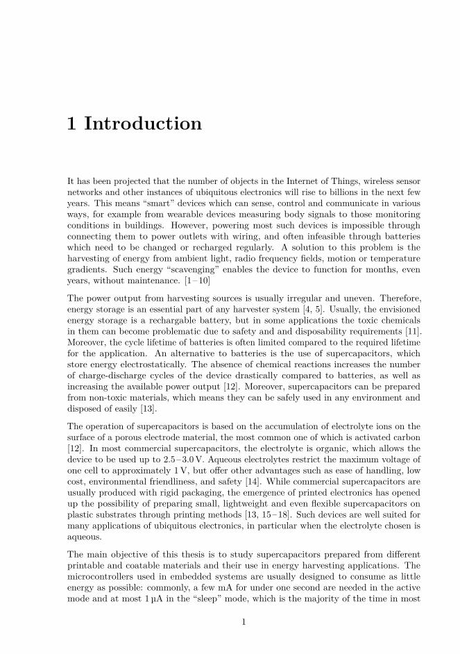
Energy harvesting from ambient sources such as light or vibrations is a promisingmethod for powering distributed and ubiquitous electronics. Harvesting requires anintermediate energy storage, for which supercapacitors are well suited due to their longcycle life compared to batteries. Moreover, supercapacitors can be prepared from non-toxicmaterials with printing methods, enabling their use in many applications.
This thesis analyzes different types of solution processed supercapacitors prepared usingdifferent materials, fabrication methods and architectures, and their use in energy har-vesting. Supercapacitors were prepared from the conventional material, activated carbon,as well as novel materials: carbon nanotubes and conducting polymer composites. Layerswere deposited by doctor blade coating and screen printing, and in the case of conductingpolymers, also electrochemical deposition. Neutral aqueous electrolytes were used in thesupercapacitors.
Carbon nanotubes (CNTs), which have both conductivity and a high surface area, offerthe possibility of preparing the supercapacitor electrodes with only one layer, withouta separate current collector. In this work, CNT supercapacitors were prepared fromblade-coated electrodes, and capacitances of 6mF/cm2 were achieved. The equivalentseries resistance (ESR) was large, 80Ω, probably due to the large amount of dispersantpolymer needed in the ink. The other novel material studied in this work was a compositeof poly(3,4-ethylenedioxythiophene) (PEDOT) and reduced graphene oxide. Symmetricsupercapacitors prepared from electropolymerized layers on plastic substrates yielded18mF/cm2 capacitance and 25Ω ESR. It was found that the reduced graphene oxideaccounts for approximately 30% of the capacitance of the composite, although morphologychanges due to its incorporation have an effect as well.
Screen-printed supercapacitors were prepared from a graphite ink as a current collector andan activated carbon based ink as the active layer. The effect of varying layer thicknesseson the device properties was examined in detail. On average, capacitance of 150mF/cm2
and ESR of 10Ω was achieved and the current collectors were found to be the main sourceof the ESR. The effect of the maximum voltage on the device properties was also tested,and while a higher voltage yielded a higher capacitance, it also led to a higher leakagecurrent as well as quicker device degradation. Based on these results, 1.0V was found tobe a good compromise for the maximum voltage of the supercapacitors.
Energy harvesting was demonstrated with a printed radio-frequency harvester. Usingtwo 450mF supercapacitors in series, a 1.2V voltage-control circuit could be operatedfor over 10 hours with a steady output. Operating an electrochromic display was alsodemonstrated with a supercapacitor charged through a solar cell module under ambientlighting.
i


Preface
This work was carried out at the Department of Electronics and Communications Engi-neering at Tampere University of Technology. The research was funded by the Academy ofFinland, the Finnish Funding Agency for Technology and Innovation (Tekes), and Jennyand Antti Wihuri Foundation. The work was also supported by Tekniikan edistämissäätiöand the Nokia Foundation.
I would like to thank my supervisor, Prof. Donald Lupo, for his guidance throughoutmy work. I am also grateful to my co-supervisor Asst. Prof. Sampo Tuukkanen for hissupport. I would like to thank my past and present colleagues in the Laboratory forFuture Electronics for the great working atmosphere; in particular I thank D.Sc. MarikaJanka, D.Sc. Petri Heljo and M.Sc. Anna Railanmaa for the many helpful and pleasantconversations. I also wish to thank my colleagues M.Sc. Miao Li, M.Sc. Juho Pörhönen,and Lic.Sc. Jari Keskinen, as well as M.Sc. Milla Suominen, Docent Pia Damlin and Prof.Carita Kvarnström of Turku University, as my work would not have been finished withouttheir invaluable help.
Finally, I thank my family for their love and support through the years. I especially wantto thank my beloved husband Jouni for always being there for me, and our daughterSonja for bringing me great joy.
Tampere, March 2017
Suvi Lehtimäki
iii


Contents
Abstract i
Preface iii
Abbreviations and symbols vii
List of publications ix
1 Introduction 1
2 Background 52.1 Basic principles of supercapacitors . . . . . . . . . . . . . . . . . . . . . . 52.2 Materials used in supercapacitors . . . . . . . . . . . . . . . . . . . . . . . 92.3 Supercapacitor characterization . . . . . . . . . . . . . . . . . . . . . . . . 122.4 Printed supercapacitors . . . . . . . . . . . . . . . . . . . . . . . . . . . . 172.5 Energy harvesting . . . . . . . . . . . . . . . . . . . . . . . . . . . . . . . 18
3 Materials and methods 213.1 Electrodes . . . . . . . . . . . . . . . . . . . . . . . . . . . . . . . . . . . . 213.2 Device fabrication . . . . . . . . . . . . . . . . . . . . . . . . . . . . . . . 223.3 Characterization . . . . . . . . . . . . . . . . . . . . . . . . . . . . . . . . 223.4 Energy harvesting . . . . . . . . . . . . . . . . . . . . . . . . . . . . . . . 23
4 Results and discussion 254.1 Activated carbon supercapacitors . . . . . . . . . . . . . . . . . . . . . . . 254.2 Novel materials . . . . . . . . . . . . . . . . . . . . . . . . . . . . . . . . . 314.3 Measurement parameter effects . . . . . . . . . . . . . . . . . . . . . . . . 344.4 Energy harvesting . . . . . . . . . . . . . . . . . . . . . . . . . . . . . . . 36
5 Summary and outlook 39
Bibliography 41
Publications 47
v


Abbreviations and symbols
AC Activated carbonASIC Application specific integrated circuitCNT Carbon nanotubeCV Cyclic voltammetryECD Electrochromic displayEDL Electric double layerEDLC Electric double layer capacitorEDS Energy-dispersive X-ray spectroscopyESR Equivalent series resistanceGCD Galvanostatic charge-dischargeGO Graphene oxideOPV Organic photovoltaicPEDOT Poly(3,4-ethylenedioxythiophene)PET Poly(ethylene terephthalate)RF Radio frequencyRFID Radio frequency identificationrGO Reduced graphene oxideSEM Scanning electron microscopyTEM Transmission electron microscopy
C CapacitanceC Complex capacitanceC ′ Real part of CC ′′ Imaginary part of CE EnergyI Electric currentQ Electric chargeRF Faradaic leakage resistanceRS Series resistancet Timeτ0 Characteristic timeV VoltageZ Complex impedanceZ ′ Real part of ZZ ′′ Imaginary part of Z
vii


List of publications
I S. Lehtimäki, M. Li, J. Salomaa, J. Pörhönen, A.Kalanti, S. Tuukkanen, D. Lupo.Performance of printable supercapacitors in an RF energy harvesting circuit. Inter-national Journal of Electrical Power & Energy Systems 58, pp. 42–46, 2014.
II S. Lehtimäki, S. Tuukkanen, J. Pörhönen, P.Moilanen, J.Virtanen, M.Honkanen,D. Lupo. Low-cost, solution processable carbon nanotube supercapacitors and theircharacterization. Applied Physics A 117(3), pp. 1329–1334, 2014.
III S. Lehtimäki, M. Suominen, P.Damlin, S. Tuukkanen, C.Kvarnström, D. Lupo.Preparation of supercapacitors on flexible substrates with electrodeposited PE-DOT/graphene composites. ACS Applied Materials & Interfaces 7(40), pp. 22137–22147, 2015.
IV S. Lehtimäki, A.Railanmaa, J.Keskinen, M.Kujala, S. Tuukkanen, D. Lupo. Prop-erties and operating voltage optimization of screen-printed aqueous supercapacitors.Accepted for publication in Scientific Reports.
ix

1 Introduction
It has been projected that the number of objects in the Internet of Things, wireless sensornetworks and other instances of ubiquitous electronics will rise to billions in the next fewyears. This means “smart” devices which can sense, control and communicate in variousways, for example from wearable devices measuring body signals to those monitoringconditions in buildings. However, powering most such devices is impossible throughconnecting them to power outlets with wiring, and often infeasible through batterieswhich need to be changed or recharged regularly. A solution to this problem is theharvesting of energy from ambient light, radio frequency fields, motion or temperaturegradients. Such energy “scavenging” enables the device to function for months, evenyears, without maintenance. [1–10]
The power output from harvesting sources is usually irregular and uneven. Therefore,energy storage is an essential part of any harvester system [4, 5]. Usually, the envisionedenergy storage is a rechargable battery, but in some applications the toxic chemicalsin them can become problematic due to safety and and disposability requirements [11].Moreover, the cycle lifetime of batteries is often limited compared to the required lifetimefor the application. An alternative to batteries is the use of supercapacitors, whichstore energy electrostatically. The absence of chemical reactions increases the numberof charge-discharge cycles of the device drastically compared to batteries, as well asincreasing the available power output [12]. Moreover, supercapacitors can be preparedfrom non-toxic materials, which means they can be safely used in any environment anddisposed of easily [13].
The operation of supercapacitors is based on the accumulation of electrolyte ions on thesurface of a porous electrode material, the most common one of which is activated carbon[12]. In most commercial supercapacitors, the electrolyte is organic, which allows thedevice to be used up to 2.5–3.0V. Aqueous electrolytes restrict the maximum voltage ofone cell to approximately 1V, but offer other advantages such as ease of handling, lowcost, environmental friendliness, and safety [14]. While commercial supercapacitors areusually produced with rigid packaging, the emergence of printed electronics has openedup the possibility of preparing small, lightweight and even flexible supercapacitors onplastic substrates through printing methods [13, 15–18]. Such devices are well suited formany applications of ubiquitous electronics, in particular when the electrolyte chosen isaqueous.
The main objective of this thesis is to study supercapacitors prepared from differentprintable and coatable materials and their use in energy harvesting applications. Themicrocontrollers used in embedded systems are usually designed to consume as littleenergy as possible: commonly, a few mA for under one second are needed in the activemode and at most 1µA in the “sleep” mode, which is the majority of the time in most
1
2 Chapter 1. Introduction
sensor applications [4]. Thus, the capacity requirement of the energy storage is on theorder of tens of millijoules, which at 1V voltage corresponds to some tens to a hundredmillifarads. Due to the linear voltage decline of capacitors on discharge, all of the storedenergy cannot be utilized and the capacity needs to be somewhat higher.
The supercapacitors presented in this thesis are prepared from both conventional andnovel materials. Using blade coating and screen-printing, as well as electropolymerization,devices are prepared on flexible plastic substrates. While this makes the devices alsopotentially flexible, that topic is a broad one including the challenges in packaging andsealing the liquid electrolyte. The detailed study of device flexibility is not within thescope of this thesis; the focus is mainly on the fabrication and performance analysis ofprintable supercapacitors.
The thesis outlines the work done in four peer-reviewed publications. In I, activated-carbonbased supercapacitors are fabricated using blade-coating, characterized, and subsequentlyused in an energy harvesting application with a printed RF harvester. Two novel materials,carbon nanotubes and conducting polymer composites with reduced graphene oxide areexplored in II and III, respectively. In the latter, a harvesting demonstration is alsoperformed using a printed organic solar cell and an electrochromic display. PublicationIV is a detailed look into the properties of screen printed supercapacitors, exploring thevariation of the capacitance, leakage current and ESR with varying layer thicknesses, aswell as looking into the effect of the maximum voltage on the properties.
Chapter 2 presents the theoretical background of the work, from the basic structure andproperties of supercapacitors to the latest reports in literature on printed supercapacitors,as well as an overview of the characterization methods. The experimental methods arepresented in Chapter 3, and the main results of the included publications are outlined inChapter 4. The final chapter gives a summary of the work as well as a future outlook ofthe research.
Contribution of the author
The publications included in this thesis are the result of collaboration. The contributionof the author is as follows:
Publication I The author designed and fabricated the supercapacitors and performedtheir electrical characterization. Miao Li prepared the printed harvester at TUT andthe ASIC was designed and fabricated at Aalto University. The author planned andperformed the harvesting measurements together with M. Li. The author analyzedthe measurement data and wrote the first version of the manuscript.
Publication II The author planned the experiment and fabricated and characterizedthe supercapacitors from the ink which was obtained from collaborators. The authorbuilt the simulation model and analyzed the measurement and simulation data.The author wrote the first version of the manuscript.
Publication III The author prepared the current collector electrodes, on which theactive layers were fabricated at the University of Turku. The author assembledsupercapacitors and performed their basic characterization and data analysis. Theauthor performed the harvesting experiment together with S. Tuukkanen. Theauthor analyzed the results and wrote the first version of the manuscript.

3
Publication IV The author planned the experiments and fabricated most of the samples.The author performed the characterization, analyzed the data and wrote the firstversion of the manuscript.

2 Background
2.1 Basic principles of supercapacitors
Supercapacitors are energy storage devices whose properties are between those of batteriesand capacitors. While the energy that can be stored in a supercapacitor is lower thanin a battery, the power capability is much larger. Supercapacitors store energy in anelectrostatic manner, without electrochemical reactions and phase changes, and as a result,the cyclability and reliability of the devices is better than that of batteries. Comparedto regular capacitors, which can provide even higher power peaks, the energy which canbe stored in supercapacitors is high: common device capacitances are many orders ofmagnitude larger than in regular capacitors, ranging from 1 to several thousand farads.[12]
Thus, supercapacitors bridge the gap between batteries and capacitors and can be utilizedin many applications where large power peaks and longer cycle lives are required. Theseinclude short-term power backup, engine ignition, portable tools and regenerative brakingin vehicles. Supercapacitors can also be used in combination with batteries to achieveboth high energy and high power capabilities; an example is electric vehicles wheresupercapacitors are able to deliver short bursts of high power as well as store brakingenergy. Using only batteries, covering the power peaks would require a greatly oversizedbattery. [19]
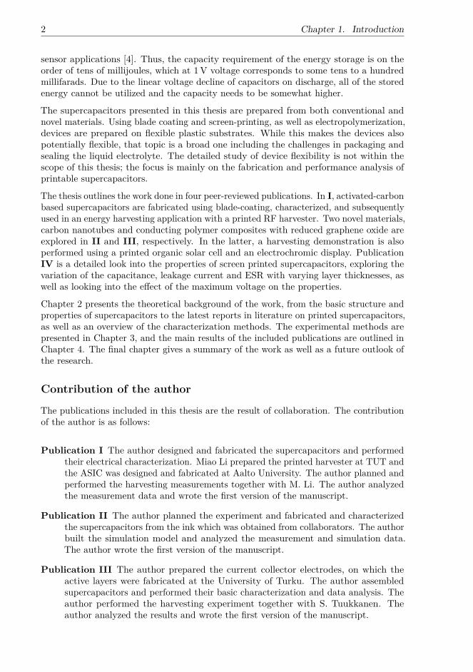
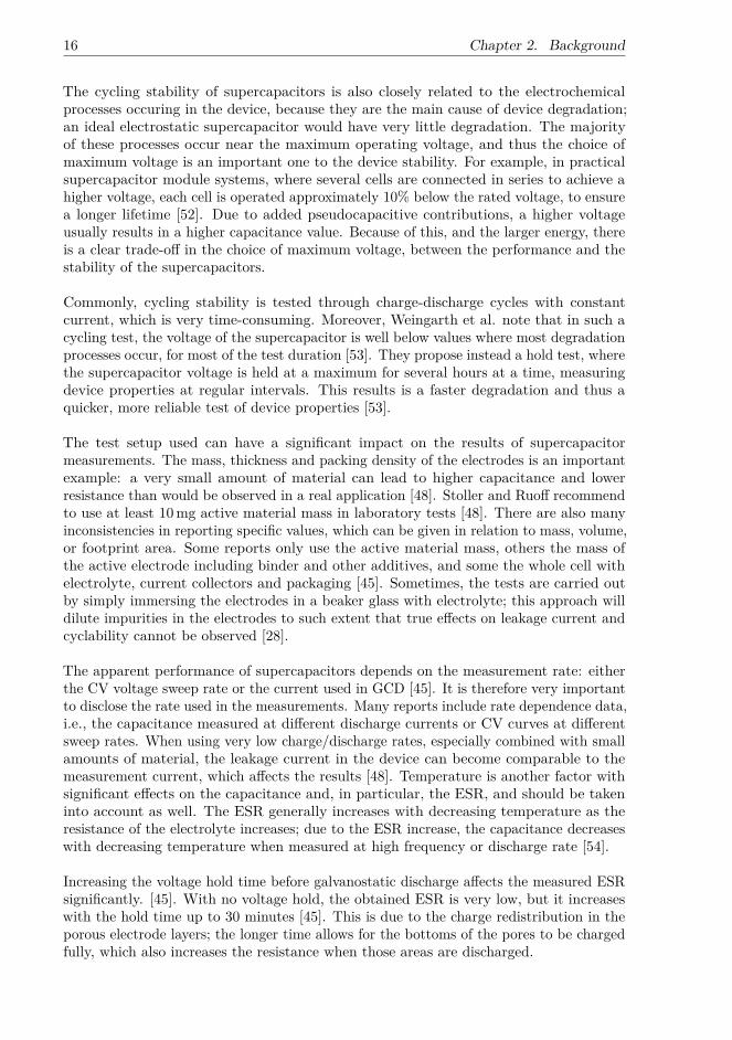
2.1.1 StructureSupercapacitors consist of two electrodes with an electrolyte and a separator film betweenthem (Fig. 2.1). The electrodes are porous with a high surface area, usually composed ofactivated carbon. When a voltage is applied between the electrodes, ions in the electrolytemove and form electric double layers (EDL), in which the charge in the electrode iscompensated for by a layer of oppositely charged ions on the surface. The voltage mustbe kept below the limit for any electrochemical reactions to occur, so that the ionsare accumulated electrostatically on the electrode surface. The double layer on eachelectrode essentially forms a plate capacitor with the distance between the charged layersin molecular dimensions. As the capacitance of a plate capacitor is inversely proportionalto this distance, the resulting capacitance is very large. The capacitance is furtherincreased by the large surface area of the porous electrode material. [12, 20]
In a supercapacitor, the two “capacitors” of the double layer electrodes are connected inseries, with the electrolyte as an ionic conductor between them. The total capacitance Cis calculated from
1C
= 1C1
+ 1C2, (2.1)
5
6 Chapter 2. Background
Figure 2.1: The structure of a supercapacitor
where C1 and C2 are the electrode capacitances. If C1 = C2, the total capacitance ishalf of the one-electrode capacitance. If the capacitances are unequal, the smaller onedominates the total capacitance – thus, it is important to have equal capacitances onthe electrodes. Single electrode capacitances can be measured in a three-electrode cellagainst a reference electrode; in this case, it should be remembered that real devices willhave at most half of the single-electrode capacitance. [12]The capacitance of an active material is often given per mass as specific capacitance(F/g), which facilitates comparison of different materials. In a symmetric device, thetotal capacitance divided by the total active material mass is then 1/4 of the singleelectrode specific capacitance, because the mass is doubled and the capacitance halveddue to the series connection [20]. When reporting material properties, it is important tonote whether the specific capacitance is from the whole device or from single-electrodemeasurements.
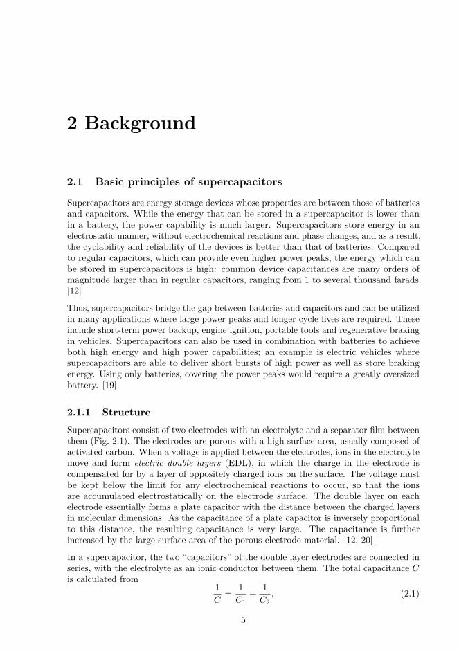
Figure 2.2: The microscopic structure of the electric double layer. OHP refers to the outer andIHP to the inner Helmholtz plane, i.e. the closest approach distance of hydrated and specificallyabsorbed ions, respectively.
Fig. 2.2 shows a microscopic depiction of the EDL structure. It is usually assumed thatthe charge in the electrode is localized very close to the surface due to the good electrical
2.1. Basic principles of supercapacitors 7
conductivity of the material. In the solution side of the double layer, the ions spreadout in a diffuse layer, which contains both negative and positive ionic species. Close tothe electrode surface lies the compact or Helmholtz layer, which consists of ions witha charge opposite to the electrode. The closest approach plane of solvated ions – i.e.,non-specifically adsorbed ions – is termed the outer Helmholz plane. Ions can also bespecifically adsorbed, losing their solvation shell, with the plane through the center ofthese ions called the inner Helmholz plane. [12, 21]
Because the double layer ions are different on the positive and negative electrodes, thedouble layers and thus capacitances of the electrodes are not identical even if the electrodestructure is symmetric. Usually, the anions are more strongly adsorbed due to their largersize and lower charge density, which results in a loosely-bound solvation shell; cations areusually more strongly solvated and thus are less likely to be specifically adsorbed. Thedifference in capacitance can be up to a factor of two. [21, 22]
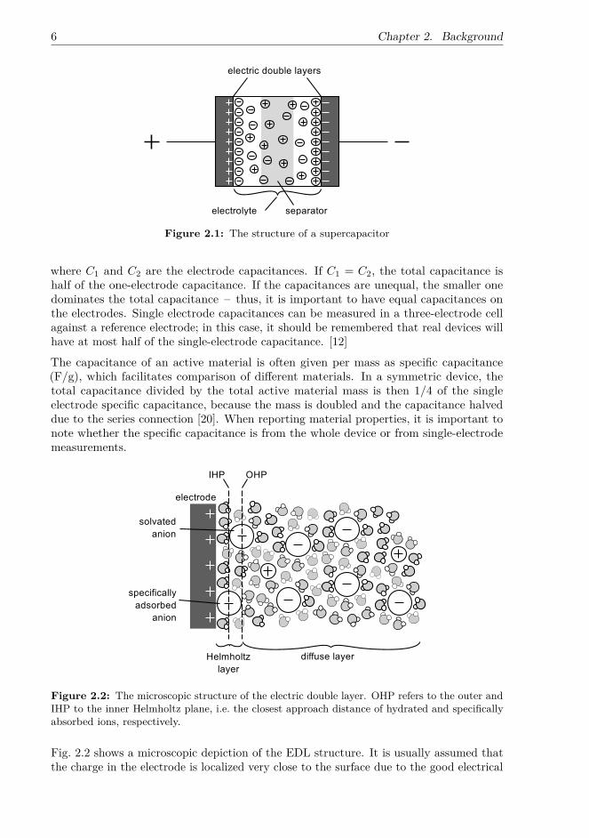
2.1.2 Resistance and leakageThe electrical properties of supercapacitors can be simplified in an equivalent circuit suchas that depicted in Fig. 2.3(a), where the EDL capacitance of each electrode, CEDL, isaccompanied by a leakage resistance due to Faradaic reactions, RF , in parallel with thecapacitance. A series resistance, RS , represents the resistance of the electrolyte solution[12, p. 483]. The leakage eventually results in the self-discharge of the capacitor. Thismeans that the capacitor cannot be stored in the charged state indefinitely. Supercapacitorself-discharge rates are larger than in batteries, where the mechanism is also somewhatdifferent [12, p. 558].
Figure 2.3: (a) An equivalent circuit describing the electrical behaviour of a supercapacitor. (b)The electrical potential in a supercapacitor when charged or discharged with a constant currentI. An IR drop occurs in the electrolyte as indicated in the figure.
The leakage resistance can arise from different processes. One obvious reason is over-charging the capacitor with a voltage that is beyond the Faradaic oxidation or reductionpotential of any constituent in the electrolyte. The most important source, however, isleakage through impurities, which are oxidized or reduced within the potential intervalused in the capacitor; similarly, functional groups on the carbon surface can also con-tribute to leakage. If the impurity concentration is low, the self-discharge process willbe diffusion-controlled, meaning that the limiting factor is the diffusion of reactant tothe electrode surface. The kinetic reversibility of the Faradaic reaction determines themagnitude of RF . Another route for the leakage is direct Ohmic leak. This can occur, for
8 Chapter 2. Background
example, if the electrode material percolates through the separator, forming a conductionpath. [12, p. 483, pp. 560–561]
The leakage mechanism can be examined through measurement of the open-circuit voltageof a charged capacitor over a long time period. The rate-limiting step of the self-dischargeprocess can be identified through the shape of the V versus time curve: linearity of Vversus log t or versus
√t, or of lnV versus t arise from activation-controlled Faradaic
reactions, diffusion-limited reactions, and Ohmic leakage, respectively [23]. Another wayof measuring leakage is through a float-current experiment, where the voltage is heldconstant by applying a small charging current matching the self-discharge rate [12, p. 562].While the mechanisms of self-discharge are not as easily identified with this method, theleakage current is an important parameter from the applications point of view.
When a supercapacitor is charged, the electric potential of the positive electrode is higherthan that of the negative electrode. The main potential drop is across the electric doublelayers (Fig. 2.3(b)). When charging or discharging the capacitor, there is also a potentialdrop across the bulk electrolyte. This is due to the resistance of the solution: ionic currentflows through the capacitor when the electric double layer ions migrate to or away fromthe electrode. This potential drop is determined by the resistance of the solution, RS ,and the discharge current, I, by V = IRS . The effect is illustrated in Fig. 2.3(b). Theresistance may be higher across the separator than in other areas of the electrolyte, andis greater in organic solvents than in water. [12, p. 106]
Additional resistance is introduced with porous electrodes (see the next section). Inpractical devices, two different contact resistances can arise: between the particles of theactive material, and between the active material and the current collector electrode. Theresistance of the bulk electrode material, the current collectors and any outside leads alsocontribute to the measured device resistance. All the different resistances are usuallygrouped into one as the equivalent series resistance (ESR), which is a common parameterin traditional capacitor devices, depicting the dielectric losses seen in high frequencies.In supercapacitors, the ESR is an important figure of merit which limits the speed atwhich the capacitor can be charged or discharged, thus restricting the maximum powerobtainable from the device. [12, p. 528]
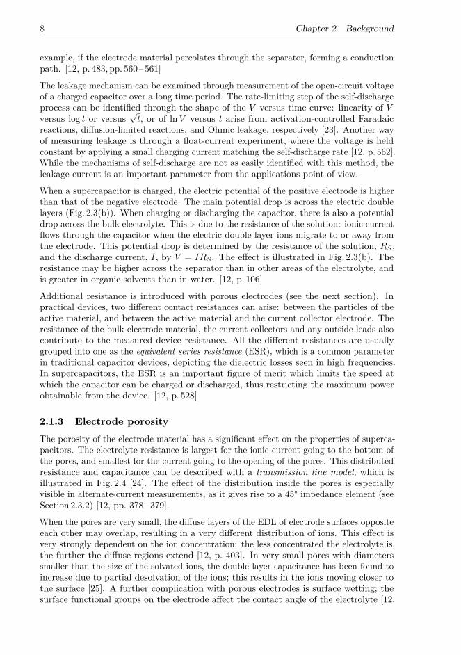
2.1.3 Electrode porosityThe porosity of the electrode material has a significant effect on the properties of superca-pacitors. The electrolyte resistance is largest for the ionic current going to the bottom ofthe pores, and smallest for the current going to the opening of the pores. This distributedresistance and capacitance can be described with a transmission line model, which isillustrated in Fig. 2.4 [24]. The effect of the distribution inside the pores is especiallyvisible in alternate-current measurements, as it gives rise to a 45° impedance element (seeSection 2.3.2) [12, pp. 378–379].
When the pores are very small, the diffuse layers of the EDL of electrode surfaces oppositeeach other may overlap, resulting in a very different distribution of ions. This effect isvery strongly dependent on the ion concentration: the less concentrated the electrolyte is,the further the diffuse regions extend [12, p. 403]. In very small pores with diameterssmaller than the size of the solvated ions, the double layer capacitance has been found toincrease due to partial desolvation of the ions; this results in the ions moving closer tothe surface [25]. A further complication with porous electrodes is surface wetting; thesurface functional groups on the electrode affect the contact angle of the electrolyte [12,
2.2. Materials used in supercapacitors 9
Figure 2.4: The distributed resistance and capacitance arising in porous electrodes.
p. 190]. Small pores may not be completely accessible to the electrolyte and thus cannotcontribute to the capacitance.When a supercapacitor is charged quickly, the whole surface of the porous electrodemay not be covered evenly with charged ions; the surface near the pore openings is fullycharged but the bottoms of the pores are not. In the circuit of Fig. 2.4 this correspondsto the leftmost capacitors being fully charged, and the rightmost charged only a little.After disconnecting the supercapacitor from the charging circuit, an internal chargeredistribution takes place: ions move further down the pores, with the accompanyingcharge on the electrode following them. This corresponds, in Fig. 2.4, to the charge onall the capacitors evening out and reaching the same value. The result is an apparentdecrease in the observed terminal voltage, which can be mistaken for leakage. [26]
2.2 Materials used in supercapacitors
Most commercial supercapacitor devices are based on activated carbon due to its lowcost, high specific surface area and chemical stability. Extensive research has beendirected at finding new alternatives to boost the specific energy and power, from speciallydesigned porous carbons and carbon nanomaterials to pseudocapacitive metal oxides andconducting polymers. The electrolytes are divided into two basic categories: aqueous andnon-aqueous. Most commercial supercapacitors rely on non-aqueous organic electrolytes,but aqueous ones are used as well.
2.2.1 CarbonActivated carbon (AC) can be prepared by pyrolysis of biomass precursors such aswood, coal, coconut shells or peat. Today, practically all activated carbon used insupercapacitors is produced from coconut shells due to its price: supercapacitor-gradeAC costs approximately $15/kg, which is very low compared to many other possibleelectrode materials. After pyrolysis, the resulting char is activated either chemically (e.g.,treatment with potassium hydroxide) or physically (high-temperature treatment withan oxidizing gas). This opens up pores in the structure and removes disordered carbonmaterial. Often, AC is blended with carbon black or graphite to improve the conductivityof the porous layer. [27–29]Highly porous carbon materials, with carefully controlled pore size distribution and porestructure, can be prepared as carbon aerogels. They are obtained through pyrolysis oforganic aerogels, the properties of which can be modified with processing conditions [29].Carbon aerogels, as well as other polymer-derived carbon materials, are more conductivethan AC, but their higher price currently prevents their use in commercial supercapacitors
10 Chapter 2. Background
[28]. Another precisely controllable way to produce porous carbon is from metal carbidessuch as titanium carbide [30]. The precursor is etched with chlorine gas, leaving behind aporous carbon structure. The process is, however, expensive compared to other methods[28].
Carbon nanomaterials, such as carbon nanotubes (CNT) and graphene, have attractedmuch attention in recent years. CNTs provide very good conductivity, but the activesurface area is mostly limited to the outsides of the nanotubes; the “pores” of the materialconsist of the interstitial spaces between nanotubes [29]. Single-walled CNTs are currentlytoo expensive for use in commercial applications, but multi-walled CNTs can be producedat approximately $50/kg with similar performance to AC [28]. One challenge with CNTsis their low solubility, which results in difficulties with the processing. Additive dispersiveagents are needed, but these then limit the performance of the electrodes.
Graphene, the one-atom-thick layer of sp2-bonded carbon, is a promising material not onlyfor supercapacitors but many other applications as well, including transistors, sensors andlithium-ion batteries [31]. Its good conductivity could enable high-power supercapacitordevices; it also has a high accessible surface area and good mechanical strength [32]. Thestructure of graphene materials is highly dependent on the preparation method – as isthe cost of the produced material. For example, mechanical exfoliation of graphite, themethod originally used to isolate graphene, leads to very high-quality graphene, but isnot feasible in large-scale production [33]. Other methods include synthesis on siliconcarbide, chemical vapour deposition, liquid-phase exfoliation of graphite and reduction ofgraphene oxide (GO). Of these, the last two are widely used in large-scale production.In liquid-phase exfoliation, intercalation of graphite by certain molecules, followed by,e.g., ultrasonication, leads to detached graphene sheets, although the yield is fairly low[33]. Graphene suffers from the same processing difficulties as CNTs in that additives areneeded to keep the individual sheets from aggregating in solution.
Oxidation of graphite produces a material which has a high degree of defects because of abroken sp2-bonded network, mainly with oxygen functionalities. This “graphite oxide” canthen be dipersed in solution to yield GO. Reduction of GO can be performed chemically,thermally or electrochemically to partly restore the graphitic structure and its conductivity[33]. While the chemical method has been the most widely used, electrochemical reductionis a very attractive choice as it does not require the use of harsh chemicals [32]. In terms ofprice and performance, graphene materials could even be competetive with AC; however,the development is still ongoing [28].
2.2.2 Pseudocapacitive materialsPseudocapacitance is a phenomenon in which charge is transferred across the double layer,as opposed to the electrostatic storage of energy in the purely double-layer capacitor. Themechanism of pseudocapacitance is Faradaic, but the reactions are fast, reversible, andtake place at the surface of the electrode [30]. In reality, some chemical reactions do takeplace also at the surfaces of carbon electrodes, for example through oxygen-containingsurface groups or impurities present in the device. The resulting pseudocapacitance canaccount for as much as 5–10% of the measured device capacitance [12, p. 188].
Pseudocapacitance can arise from a number of different mechanisms. One mechanism ispotential-dependent electrodeposition, i.e. deposition of atoms on the electrode surfacefrom solution through a Faradaic reaction. If the extent of oxidation/reduction of a metaloxide film depends on the potential, pseudocapacitance can arise. A common example
2.2. Materials used in supercapacitors 11
of this is RuO2 on ruthenium surface, but the very high cost of the metal prohibits itspractical use. Other transition metals with this property, such as manganese, have beenextensively studied due to the lower cost. Another type of pseudocapacitance blurs theline between pseudocapacitive supercapacitors and batteries: intercalation of lithium ionsinto the electrode lattice. [34, pp. 221–222]
Pseudocapacitance is also observed with conducting polymers where the applied potentialresults in the charging of the polymer, doping it with anions (oxidized form) and cations(reduced form) [34, pp. 221–222]. The extent of oxidation or reduction depends on thepotential, as with other types of pseudocapacitance. The most widely studied conductingpolymers are polyaniline, polypyrrole and derivatives of polythiophene, the most popularof which is poly(3,4-ethylenedioxythiophene) (PEDOT) [35]. Supercapacitors basedon conducting polymers exhibit good reversibility, but they usually suffer from poorcyclability due to volume changes during the reactions – which is a limitation in batteriesas well. One solution to this has been to form composites with, for example, carbonnanomaterials, which improves the stability [35].
2.2.3 ElectrolytesThere are two basic categories of electrolytes used in supercapacitors: aqueous and organic.Aqueous electrolytes perform better in terms of conductivity as well as cost, safety andease of handling, but the electrochemical window (voltage window between oxidation andreduction of the solvent) is only 1.23V [36]. The maximum voltage is very important,as the energy stored in a capacitor is proportional to the square of the voltage. Dueto this, most commercial supercapacitor manufacturers use organic electrolytes, mainlyacetonitrile and propylene carbonate, which can reach voltages of 2.5–3V [30]. Themost popular organic salts consist of lithium or tetra-alkylammonium ions as cations andtetrafluoroborate, perchlorate or hexafluorophosphate ions as anions [30, 37].
Stacking supercapacitor cells into modules is one way to increase the obtainable voltagewith aqueous electrolytes and this has been used in commercial supercapacitor modules[37]. Common aqueous electrolytes are strong acids and bases, usually sulfuric acid orpotassium hydroxide, due to their very high conductivity. Alkali salts such as KCl, NaCland NaSO4 have also been used due to the less corrosive nature of the neutral solutions[38]. One way to widen the electrochemical window of an aqueous electrolyte is to build anasymmetric supercapacitor from, for example, carbon and the pseudocapacitive manganeseoxide. Such a configuration uses the hydrogen/oxygen gas evolution overpotential, whichdepends strongly on the electrode materials [39]. Aqueous NaSO4 has been reported toenable 1.6V or even 1.9V voltages in symmetric carbon-carbon supercapacitors, withdeaereated solvent and special pretreatment of the electrode materials [38, 40].
In recent years, ionic liquids have generated much interest as electrolytes. Ionic liquidsare organic salts that have unusually low melting points, many of them liquid at roomtemperature. The low melting point is a result of at least one of the ions being large andunsymmetrical. The most important use of ionic liquids is in organic synthesis, wherethey are considered ‘green solvents’ due to their nonexistent vapour pressures and non-flammability. Ionic liquids are very stable, and being molten salts, conduct electricity well.Many ionic liquids, such as 1-ethyl-3-methylimidazolium bis(triluoromethylsulfate)imide(EMITFSI), have exceptionally wide electrochemical windows (as high as 4 V), makingthem attractive materials for supercapacitors. [41, 42]
Gel electrolytes are another interesting type of electrolyte to be used in supercapacitors.
12 Chapter 2. Background
Their solid-like structure removes the danger of electrolyte leakage, while the mobileions enable conduction within the gel. A further advantage is that there is no needfor a separator layer, since the gel itself functions as a separator. Common aqueousgel electrolytes are, for example, mixtures of poly(vinyl alcohol) (PVA) with potassiumhydroxide or sulfuric acid [43, 44].
If a liquid electrolyte is used, a separator layer must be inserted between the electrodesto avoid short-circuiting the device. To ensure good ionic conductivity, the separatorshould be very porous and all eletrolyte constituents should be able to pass through it.Commonly, glassy fibrous separators, cellulose or filter paper are used.
2.3 Supercapacitor characterization
The three most common ways to characterize supercapacitors are cyclic voltammetry (CV),galvanostatic, i.e., constant current, charge-discharge (GCD) and impedance spectroscopy.CV is well suited to characterizing the properties of supercapacitor materials, especiallyin a 3-electrode setup. GCD is the recommended method for testing real device function,and impedance spectroscopy to study frequency dependence and transient processes insupercapacitors. [45]
Many parameters affect the measurement results, such as electrode thickness, currentcollector material and charging time before discharge. There have been intensive effortsto standardize supercapacitor measurements [45–47], but a single standard is yet to beadopted. Thus, when reporting properties, it is important to note the exact measurementconditions and procedures. [45, 48]
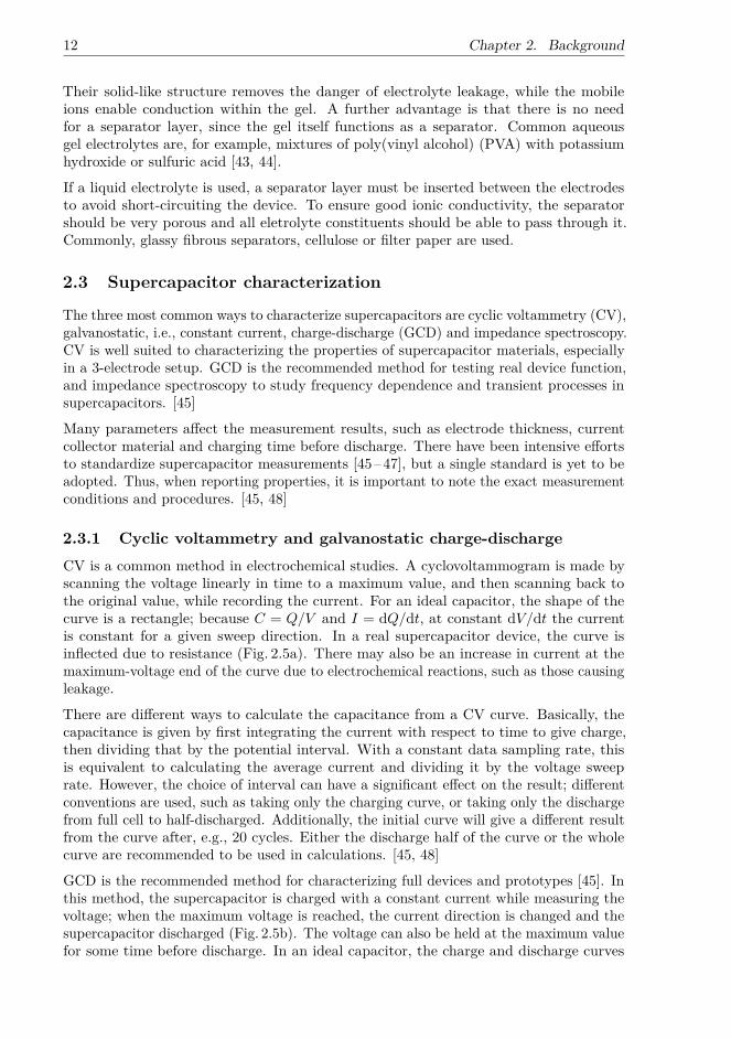
2.3.1 Cyclic voltammetry and galvanostatic charge-dischargeCV is a common method in electrochemical studies. A cyclovoltammogram is made byscanning the voltage linearly in time to a maximum value, and then scanning back tothe original value, while recording the current. For an ideal capacitor, the shape of thecurve is a rectangle; because C = Q/V and I = dQ/dt, at constant dV/dt the currentis constant for a given sweep direction. In a real supercapacitor device, the curve isinflected due to resistance (Fig. 2.5a). There may also be an increase in current at themaximum-voltage end of the curve due to electrochemical reactions, such as those causingleakage.
There are different ways to calculate the capacitance from a CV curve. Basically, thecapacitance is given by first integrating the current with respect to time to give charge,then dividing that by the potential interval. With a constant data sampling rate, thisis equivalent to calculating the average current and dividing it by the voltage sweeprate. However, the choice of interval can have a significant effect on the result; differentconventions are used, such as taking only the charging curve, or taking only the dischargefrom full cell to half-discharged. Additionally, the initial curve will give a different resultfrom the curve after, e.g., 20 cycles. Either the discharge half of the curve or the wholecurve are recommended to be used in calculations. [45, 48]
GCD is the recommended method for characterizing full devices and prototypes [45]. Inthis method, the supercapacitor is charged with a constant current while measuring thevoltage; when the maximum voltage is reached, the current direction is changed and thesupercapacitor discharged (Fig. 2.5b). The voltage can also be held at the maximum valuefor some time before discharge. In an ideal capacitor, the charge and discharge curves
2.3. Supercapacitor characterization 13
are linear. This is also the case for most supercapacitors with little pseudocapacitivebehaviour, as well as many pseudocapacitors [45].
0 . 0 0 . 2 0 . 4 0 . 6 0 . 8 1 . 0- 1 5- 1 0- 505
1 01 5
0 2 4 6 80 . 00 . 20 . 40 . 60 . 81 . 0
0 2 4 60 . 5
1 . 0
1 . 5
Curre
nt (m
A)
V o l t a g e ( V )
Volta
ge (V
)T i m e ( m i n )
Volta
ge (V
)
T i m e ( s )
I R d r o pa ) b ) c )
Figure 2.5: Examples of supercapacitor measurements: a) CV curve, b) galvanostatic charge-discharge, and c) galvanostatic discharge after voltage hold with extrapolation to find the correctIR drop value.
In the beginning of the discharge, there is a drop in voltage due to the ESR of the device,corresponding to V = R∆I, where ∆I is the change in current. The ESR can thenbe calculated from this voltage drop. If the current is zero before the discharge, ∆I isthe discharge current; if there is a quick switch from charging at I to dicharging at I,the change in current is ∆I = 2I [45]. However, in supercapacitors there is usually anadditional, more gradual voltage drop after the initial one (Fig. 2.5c) due to the slowerresponse of the electrolyte in the pores of the device. Because of this, it is recommendedthat the straight part of the discharge curve is extrapolated to the beginning point of thedischarge, and that value used for calculation [46]. The extrapolated IR drop value canbe up to twice that of the instantaneous one [47].
The capacitance is calculated from the discharge curve as:
C = I × t2 − t1V2 − V1
, (2.2)
between points 1 and 2 on the discharge curve, or by linear fit of the data in this interval.In the IEC standard [46], these points are where the capacitor voltage is 80% and 40% ofthe fully charged device. The capacitance can also be calculated from the whole curveafter the IR drop, which yields the same result when the curve is linear [45]. The choiceof discharge current affects the results of GCD. In general, increasing the current resultsin the decrease of both capacitance and ESR [45]. In the IEC standard, the current isdefined with regard to the capacitance in four application classes [46].
2.3.2 Impedance spectroscopyImpedance spectroscopy is a versatile tool for characterizing many transient processesin electrochemical systems [49]. The method consists of applying a small (5–10mV)alternating voltage v(t) and measuring the resulting alternating current i(t), optionallyon top of a DC offset voltage. The voltage and current are related by
v(t) = Zi(t) , (2.3)
where Z is the complex impedance. It can be represented as a magnitude and phaseangle (|Z| and φ), or as real and imaginary components (Z ′ and Z ′′). The measurement
14 Chapter 2. Background
frequency is swept from about 1mHz to 1MHz [49], resulting in a spectrum of impedancedata. The real part of the impedance is related to the device resistance: sometimes, thevalue of Z ′ at 1 kHz is taken as the ESR [47]. This value can, however, be significantlylower than that measured with the galvanostatic method [47].
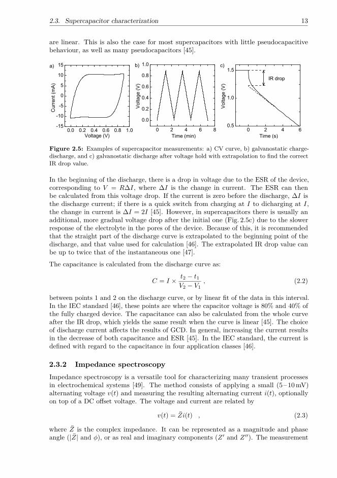
An example impedance curve, plotted as Z ′′ versus Z ′ (a Nyquist plot), is shown inFig. 2.6. The values of Z ′′ are negative for a capacitor, so the plot is usually drawn witha negative vertical axis. As both axes are in units of Ω, the axis spacing should be thesame. At low frequency, the plot tends toward a vertical line, which is characteristic ofan ideal capacitor. The shift in the Z ′ direction is indicative of a series resistance.
Figure 2.6: Example of a Nyquist plot of impedance data; b is a close-up view of a.
At medium frequencies, there is a section of the Nyquist plot with approximately 45° angle.This arises due to the transmission line behaviour (Section 2.1.3) of the porous electrodematerial [34, p. 484]. The width of this area depends on the electrode thickness [50]. Atthe highest frequencies, a semicircle is often observed in supercapacitor measurements.The cause is a parallel RC-element in the system [12, p. 494]. It has been shown by Portetet al. that the most likely reason is an imperfect electrical contact between the currentcollector and the active material: the contact interface effectively contains a resistanceand an interface capacitance in parallel [51]. In reality, the semicircle is rarely a perfectone with its center on the real axis: different distributed elements and processes withdifferent relaxation times can distort the shape of the curve [49].
The impedance data can be used to calculate a complex capacitance, C = C ′ + iC ′′
according to [50]
C ′ = − Z ′′
2πf |Z|2and C ′′ = Z ′
2πf |Z|2. (2.4)
The real part, C ′, is related to the device capacitance and its value at the lowest frequenciescorresponds to the galvanostatically measured capacitance. The imaginary part, C ′′, isrelated to resistive losses in the device. Plotted against the frequency, C ′′ goes through amaximum at some frequency f0; the reciprocal of this frequency is a characteristic time,τ0, which describes how quickly the supercapacitor can be charged and discharged withover 50% efficiency [25].
2.3. Supercapacitor characterization 15
2.3.3 Energy and powerThe energy stored in a capacitor is calculated from
E = 12CV
2max , (2.5)
where V is the maximum voltage. The formula applies to supercapacitors as well, when theGCD is linear [45]. However, in most applications energy drawn from the supercapacitoris only useful if the voltage is over, e.g., 0.5Vmax [47, 48]. In this case, only 75% of thestored energy can be used, and the formula becomes [47]
E = 38CV
2max . (2.6)
This is still a simplified form, as a full description of the energy capability requiresthe relationship between power and energy: the usable energy usually decreases withincreasing power [47]. The energy is commonly reported normalized to the mass or volumeof the device or the active material; the values in commercial supercapacitors range from 1to 6Wh/kg for full devices. Taking into account only the active mass (e.g., the activatedcarbon in the device), 15 to 25Wh/kg is obtained. [45]
The maximum power that can be drawn from a supercapacitor occurs when the loadresistance is equal to the ESR (match impedance). In this case, the power is
Pmax = V 2max
4× ESR . (2.7)
This is the value most often reported, but the usable power in real applications is closerto half of Pmax. In a pulse power measurement, only approximately 1/10 of Pmax isavailable. Specific power values for commercial supercapacitors range from 2 to 20 kW/kgfor full devices and from 20 to 120 kW/kg for only the active material. [45]
2.3.4 Other factors affecting supercapacitor performanceThe leakage pathways described in Sec. 2.1.2 result in an eventual discharge of thesupercapacitor, and thus the magnitude of leakage is an important parameter to measure.There are two basic ways for leakage determination: a float current method, and aself-discharge method [23].
In the float current method, the supercapacitor is charged to the maximum voltage andheld there for a period of time, ranging from 1 hour to 72 hours, to ensure that theelectrode surface is charged evenly [45, 46]. Due to leakage, a small float current is neededto maintain the voltage – this current is then recorded as the leakage current of thedevice, after a specified time [45, 46]. In the self-discharge method, the supercapacitor isfully charged, again holding the maximum voltage for some hours to ensure full charging[45, 46]. After this, the device is disconnected and its voltage monitored over time. Forcontinuous measurement, the voltmeter used should have a very large input impedance.Alternatively, the voltage can only be measured at certain intervals and the supercapacitordisconnected between measurements. The two leakage current measurement methodsare not equivalent: the reactions causing leakage depend on voltage, so that at a highervoltage more reactions occur. In the self-discharge test, the declining voltage affects whichleakage processes can take place.
16 Chapter 2. Background
The cycling stability of supercapacitors is also closely related to the electrochemicalprocesses occuring in the device, because they are the main cause of device degradation;an ideal electrostatic supercapacitor would have very little degradation. The majorityof these processes occur near the maximum operating voltage, and thus the choice ofmaximum voltage is an important one to the device stability. For example, in practicalsupercapacitor module systems, where several cells are connected in series to achieve ahigher voltage, each cell is operated approximately 10% below the rated voltage, to ensurea longer lifetime [52]. Due to added pseudocapacitive contributions, a higher voltageusually results in a higher capacitance value. Because of this, and the larger energy, thereis a clear trade-off in the choice of maximum voltage, between the performance and thestability of the supercapacitors.
Commonly, cycling stability is tested through charge-discharge cycles with constantcurrent, which is very time-consuming. Moreover, Weingarth et al. note that in such acycling test, the voltage of the supercapacitor is well below values where most degradationprocesses occur, for most of the test duration [53]. They propose instead a hold test, wherethe supercapacitor voltage is held at a maximum for several hours at a time, measuringdevice properties at regular intervals. This results is a faster degradation and thus aquicker, more reliable test of device properties [53].
The test setup used can have a significant impact on the results of supercapacitormeasurements. The mass, thickness and packing density of the electrodes is an importantexample: a very small amount of material can lead to higher capacitance and lowerresistance than would be observed in a real application [48]. Stoller and Ruoff recommendto use at least 10mg active material mass in laboratory tests [48]. There are also manyinconsistencies in reporting specific values, which can be given in relation to mass, volume,or footprint area. Some reports only use the active material mass, others the mass ofthe active electrode including binder and other additives, and some the whole cell withelectrolyte, current collectors and packaging [45]. Sometimes, the tests are carried outby simply immersing the electrodes in a beaker glass with electrolyte; this approach willdilute impurities in the electrodes to such extent that true effects on leakage current andcyclability cannot be observed [28].
The apparent performance of supercapacitors depends on the measurement rate: eitherthe CV voltage sweep rate or the current used in GCD [45]. It is therefore very importantto disclose the rate used in the measurements. Many reports include rate dependence data,i.e., the capacitance measured at different discharge currents or CV curves at differentsweep rates. When using very low charge/discharge rates, especially combined with smallamounts of material, the leakage current in the device can become comparable to themeasurement current, which affects the results [48]. Temperature is another factor withsignificant effects on the capacitance and, in particular, the ESR, and should be takeninto account as well. The ESR generally increases with decreasing temperature as theresistance of the electrolyte increases; due to the ESR increase, the capacitance decreaseswith decreasing temperature when measured at high frequency or discharge rate [54].
Increasing the voltage hold time before galvanostatic discharge affects the measured ESRsignificantly. [45]. With no voltage hold, the obtained ESR is very low, but it increaseswith the hold time up to 30 minutes [45]. This is due to the charge redistribution in theporous electrode layers; the longer time allows for the bottoms of the pores to be chargedfully, which also increases the resistance when those areas are discharged.
2.4. Printed supercapacitors 17
2.4 Printed supercapacitors
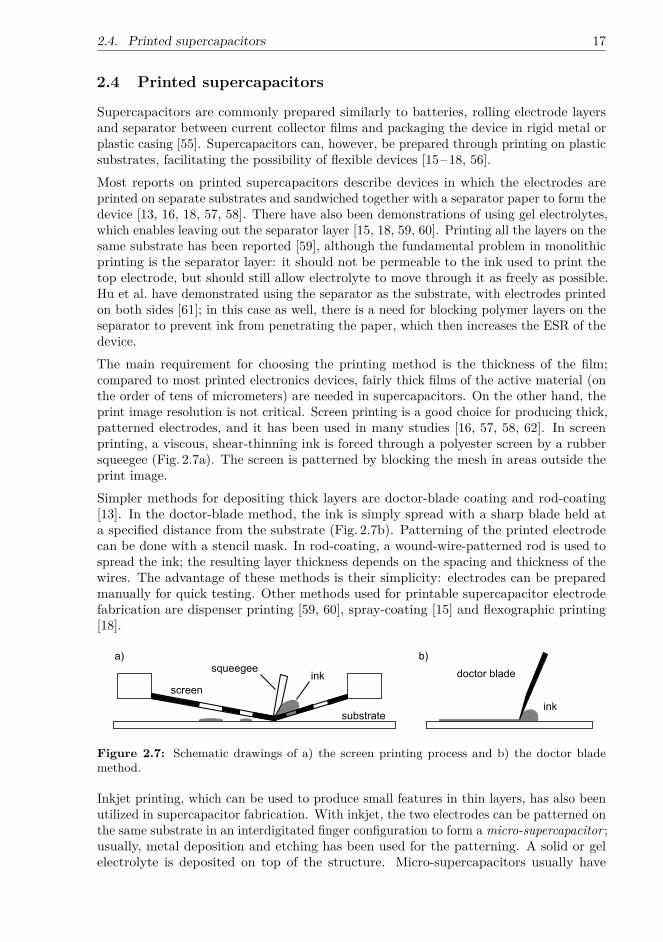
Supercapacitors are commonly prepared similarly to batteries, rolling electrode layersand separator between current collector films and packaging the device in rigid metal orplastic casing [55]. Supercapacitors can, however, be prepared through printing on plasticsubstrates, facilitating the possibility of flexible devices [15–18, 56].Most reports on printed supercapacitors describe devices in which the electrodes areprinted on separate substrates and sandwiched together with a separator paper to form thedevice [13, 16, 18, 57, 58]. There have also been demonstrations of using gel electrolytes,which enables leaving out the separator layer [15, 18, 59, 60]. Printing all the layers on thesame substrate has been reported [59], although the fundamental problem in monolithicprinting is the separator layer: it should not be permeable to the ink used to print thetop electrode, but should still allow electrolyte to move through it as freely as possible.Hu et al. have demonstrated using the separator as the substrate, with electrodes printedon both sides [61]; in this case as well, there is a need for blocking polymer layers on theseparator to prevent ink from penetrating the paper, which then increases the ESR of thedevice.The main requirement for choosing the printing method is the thickness of the film;compared to most printed electronics devices, fairly thick films of the active material (onthe order of tens of micrometers) are needed in supercapacitors. On the other hand, theprint image resolution is not critical. Screen printing is a good choice for producing thick,patterned electrodes, and it has been used in many studies [16, 57, 58, 62]. In screenprinting, a viscous, shear-thinning ink is forced through a polyester screen by a rubbersqueegee (Fig. 2.7a). The screen is patterned by blocking the mesh in areas outside theprint image.Simpler methods for depositing thick layers are doctor-blade coating and rod-coating[13]. In the doctor-blade method, the ink is simply spread with a sharp blade held ata specified distance from the substrate (Fig. 2.7b). Patterning of the printed electrodecan be done with a stencil mask. In rod-coating, a wound-wire-patterned rod is used tospread the ink; the resulting layer thickness depends on the spacing and thickness of thewires. The advantage of these methods is their simplicity: electrodes can be preparedmanually for quick testing. Other methods used for printable supercapacitor electrodefabrication are dispenser printing [59, 60], spray-coating [15] and flexographic printing[18].
Figure 2.7: Schematic drawings of a) the screen printing process and b) the doctor blademethod.
Inkjet printing, which can be used to produce small features in thin layers, has also beenutilized in supercapacitor fabrication. With inkjet, the two electrodes can be patterned onthe same substrate in an interdigitated finger configuration to form a micro-supercapacitor ;usually, metal deposition and etching has been used for the patterning. A solid or gelelectrolyte is deposited on top of the structure. Micro-supercapacitors usually have
18 Chapter 2. Background
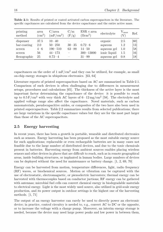
Table 2.1: Results of printed or coated activated carbon supercapacitors in the literature. Thespecific capcitances are calculated from the device capacitance and the entire active mass.
printing area C/area C/m ESR× area electrolyte Vmax Ref.method (cm2) (mF/cm2) (F/g) (Ωcm2) (V)dispenser 37.5 10–40 – – organic 2.5 [60]bar-coating 2.0 50–250 30–35 0.72–6 aqueous 1.2 [13]screen 4–6 190–510 63–88 14–50 aqueous gel 1.0 [58]screen 56 44–173 – 300–13000 ionic liquid 1.5 [16]flexographic 25 0.72–4 – 31–99 aqueous gel 0.8 [18]
capacitances on the order of 1 mF/cm2 and they can be utilized, for example, as smallon-chip energy storages in ubiquitous electronics. [63, 64]
Literature reports of printed supercapacitors based on AC are summarized in Table 2.1.Comparison of such devices is often challenging due to differences in measurementsetups, procedures and calculations [65]. The thickness of the active layer is the mostimportant factor determining the capacitance of the device: it is possible to reachup to 0.5F/cm2 with very thick AC layers of 6–12mg/cm2 [58]. The electrolyte andapplied voltage range also affect the capacitance. Novel materials, such as carbonnanomaterials, pseudocapacitive oxides, or composites of the two have also been used inprinted supercapacitors. Table 2.2 summarizes results from selected publications; thereare large variations in the specific capacitance values but they are for the most part largerthan those of the AC supercapacitors.
2.5 Energy harvesting
In recent years, there has been a growth in portable, wearable and distributed electronicssuch as sensors. Energy harvesting has been proposed as the most suitable energy sourcefor such applications; replaceable or even rechargable batteries are in many cases notfeasible due to the large number of distributed devices, and due to the toxic chemicalspresent in batteries. Harvesting energy from ambient sources enables placing wirelesssensors and other devices in places that are difficult to reach, such as in remote geographicalareas, inside building structures, or implanted in human bodies. Large numbers of devicescan be deployed without the need for maintenance or battery change. [1, 2, 69, 70]
Energy can be harvested from motion, temperature differences, light, radio frequency(RF) waves, or biochemical sources. Motion or vibration can be captured with theuse of electrostatic, electromagnetic, or piezoelectric harvesters; thermal energy can beharvested with thermocouples based on conductor juctions; RF energy can be gatheredwith antennas; microbial fuel cells can convert chemical energy in biodegradable materialsto electrical energy. Light is the most widely used source, also utilized in grid-scale energyproduction, and its power output in outdoor settings is the highest one of the harvestingmethods. [1, 71]
The output of an energy harvester can rarely be used to directly power an electronicdevice; in practice, control circuitry is needed to, e.g., convert AC to DC or the opposite,or to increase the voltage with a charge pump. Moreover, an interim energy storage isneeded, because the device may need large power peaks and low power in between them,
2.5. Energy harvesting 19
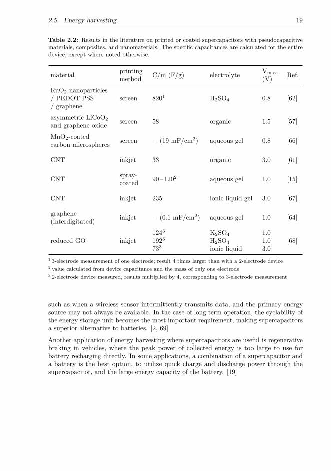
Table 2.2: Results in the literature on printed or coated supercapacitors with pseudocapacitivematerials, composites, and nanomaterials. The specific capacitances are calculated for the entiredevice, except where noted otherwise.
material printing C/m (F/g) electrolyte Vmax Ref.method (V)RuO2 nanoparticles
screen 8201 H2SO4 0.8 [62]/ PEDOT:PSS/ grapheneasymmetric LiCoO2 screen 58 organic 1.5 [57]and graphene oxideMnO2-coated screen – (19 mF/cm2) aqueous gel 0.8 [66]carbon microspheres
CNT inkjet 33 organic 3.0 [61]
CNT spray- 90–1202 aqueous gel 1.0 [15]coated
CNT inkjet 235 ionic liquid gel 3.0 [67]
graphene inkjet – (0.1 mF/cm2) aqueous gel 1.0 [64](interdigitated)
reduced GO inkjet1243 K2SO4 1.0
[68]1923 H2SO4 1.0733 ionic liquid 3.0
1 3-electrode measurement of one electrode; result 4 times larger than with a 2-electrode device2 value calculated from device capacitance and the mass of only one electrode3 2-electrode device measured, results multiplied by 4, corresponding to 3-electrode measurement
such as when a wireless sensor intermittently transmits data, and the primary energysource may not always be available. In the case of long-term operation, the cyclability ofthe energy storage unit becomes the most important requirement, making supercapacitorsa superior alternative to batteries. [2, 69]
Another application of energy harvesting where supercapacitors are useful is regenerativebraking in vehicles, where the peak power of collected energy is too large to use forbattery recharging directly. In some applications, a combination of a supercapacitor anda battery is the best option, to utilize quick charge and discharge power through thesupercapacitor, and the large energy capacity of the battery. [19]

3 Materials and methods
In this chapter, the sample preparation and characterization is is described briefly. Moredetailed descriptions of the experiments are given in the publications I– IV. The substratematerial in all samples was poly(ethylene terephtalate) (PET), which has very goodsurface properties in terms of printing, as well as good heat stability.
3.1 Electrodes
The current collectors in I and III were prepared by first evaporating a copper orsilver layer on the substrate, then blade-coating a layer of conducting graphite ink(Henkel/Acheson Electrodag PF407C) on top of the metal. The graphite layer protectsthe metal layer from corrosion. In IV, only the graphite ink was used as current collector:two layers were printed with a semiautomatic screen printer.Two commercially available activated carbons were used in this work as active layer:Norit DLC Super 50 [I], and Kuraray YP-80F [IV]. The former has a specific surfacearea of approximately 2000m2/g and the latter 2100m2/g according to the supplier. TheACs were formulated into inks using carboxymethyl cellulose as binder with Norit andshrimp-shell derived chitosan with Kuraray, both at approximately 5% of the ink drymass. The solvent for the ink was water, which facilitates a very simple ink handling andcleanup, but which evaporates very quickly compared to typical screen printing solvents.The Norit ink was blade-coated on the current collector, which enables using only smallamounts of ink at a time and carrying out the coating before the ink dries. The Kurarayink was screen printed; during the print, deionized water was sprayed on the screenintermittently to prevent the ink from drying on the screen. This, however, resulted insome variation of the printed layer thicknesses, as the ink was alternately concentratedthrough water evaporation and diluted through the addition of water [IV].A carbon nanotube (CNT) ink was obtained from Morphona Ltd (Finland). The ink isan aqueous dispersion of multi-walled CNTs in water with a xylan hemicellulose polymeras a dispersant/binder. The polymer constituted approximately a third of the ink drymass; the large amount is needed to disperse the nanotubes, which otherwise tend toaggregate. The ink was blade-coated into 1.4 cm wide electrodes, using multiple coatingpasses to achieve a sufficiently conducting layer. The ink functioned as both the currentcollector and active material, so other layers were not needed. [II]PEDOT and and its composites with graphene oxide (GO) were prepared at the Uni-versity of Turku on metal/graphite current collectors. PEDOT was prepared throughelectropolymerization of 3,4-ethylenedioxythiophene in an ionic liquid; adding dispersedGO in the solution resulted in the negatively charged GO flakes being embedded into thepolymer layer as counterions. Electrochemical reduction was used to convert the GO to
21
22 Chapter 3. Materials and methods
reduced graphene oxide (rGO). The charge consumed by the polymerization was keptconstant in all samples, so that layers with similar PEDOT content were produced. Bothpotentiostatic and cyclic voltammetry electropolymerization methods were tested, andthe CV method found to produce better layers. [III]
3.2 Device fabrication
The supercapacitors were assembled from two similar electrodes and a separator paper,which were sandwiched together. The electrodes and separator were saturated withaqueous LiCl (I) or NaCl (II– IV) before assembly, and the lamination of the layers doneby carefully rolling the top electrode on the bottom one in such a way that the amountof air trapped in the device was minimized. In I– III, the electrodes were placed in a90° angle with respect to each other with the square-shaped active areas overlapping.The electrodes were 1.4 cm or 2.0 cm wide, yielding 2 and 4 cm2 active areas, respectively.In IV, the electrodes were wider (2.0 cm) and shorter, and the assembly done with ahead-on configuration; the active area was 1.8 cm wide and 1.0 cm long.
The substrates were sealed together with an adhesive film (in I– III), which was cut asa square gasket and placed around the active area. In IV, heat-sealing was used; asPET itself could not be heat-sealed, an ethylene-copolymer dispersion in water (ParameltAquaseal) was applied on the edges of the substrate, dried, and the device edges heat-sealed.
3.3 Characterization
Cyclic voltammetry (CV) and galvanostatic charge-discharge (GCD) were performedwith a Zahner Zennium potentiostat (I– III) or a Maccor 4300 battery test system (IV).The IEC standard [46] was used as a basis for the characterization: the capacitanceswere derived from the discharge curve at constant current after a 30-minute voltagehold, except for I where a 5-minute hold was used. The maximum voltage was 0.9V forall measurements. Additionally, a voltage test was performed with the screen printedsupercapacitors to examine the effect of the maximum voltage (from 0.8V to 1.2V) onthe device properties.
The ESR was calculated from the IR drop of a GCD curve with 10 times higher currentthan that used for the capacitance measurement [46]. A linear fit was made to thedischarge curve between 1% and 20% of the discharge time; the fit at this interval wasvisually estimated to best correspond to the fitting procedure described in [46]. Theleakage current was recorded after 30min or 1 h hold at the maximum voltage.
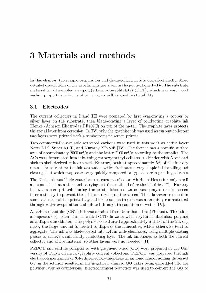
In the measurements performed on the Maccor system (IV), a long measurement programcould be used, covering three charge-discharge cycles, a 30-minute voltage hold anddischarge for capacitance/ESR determination, and a 1-hour voltage hold for leakagecurrent determination. These steps were repeated three times for three different currents(here, 1mA, 3mA and 10mA), after which CV curves were measured at 100mV/s,50mV/s, 10mV/s and 5mV/s, four cycles for each. In IV, discharge at 1mA was used forcapacitance calculation and discharge at 10mA used for ESR calculation. The reportedleakage current was taken from the end of the third 1-hour segment. The measurement isillustrated in Fig. 3.1.
3.4. Energy harvesting 23
0 1 2 3 4 5 60 . 00 . 20 . 40 . 60 . 81 . 0
Vo
ltage
(V)
T i m e ( h )
c u r r e n t c o n t r o l v o l t a g e c o n t r o l
Figure 3.1: The measurement program used in IV. The voltage-controlled part in the end isthe CV measurement.
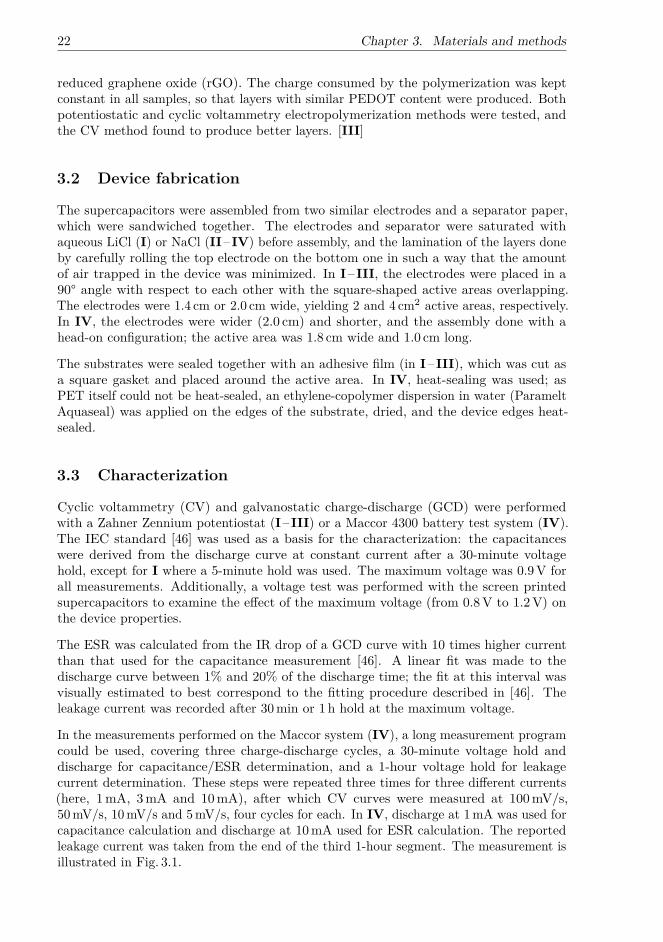
Figure 3.2: Schematics of the harvester a) charging circuit and b) operation circuit. Adaptedfrom I.
Impedance spectrocopy was performed with the Zahner Zennium potentiostat in thefrequency range from 10mHz to 1MHz. An amplitude of 5mV and offset of 0V wereused. The samples were discharged well by short circuiting prior to the measurement.
3.4 Energy harvesting
The metal/graphite AC supercapacitors were used in an energy harvesting demonstrationwith a printed RF harvester. A circuit diagram of the experiment setup is shown inFig. 3.2. An RFID reader was used for charging the supercapacitor through a printedantenna and rectifier; two reader –antenna distances were used to give the rectifier eithera high or a low input signal amplitude. Two similar supercapacitors were connected inseries to reach a higher voltage; two different device sizes were tested. [I]
The supercapacitor operation after RF harvesting was then demonstrated with anapplication-specific integrated circuit (ASIC), which gives a steady output of 1.2V,suitable for powering, e.g., a small sensor. A 1MΩ load (RL) was connected to the ASICoutput and the voltages of the supercapacitors and the output monitored through probes
24 Chapter 3. Materials and methods
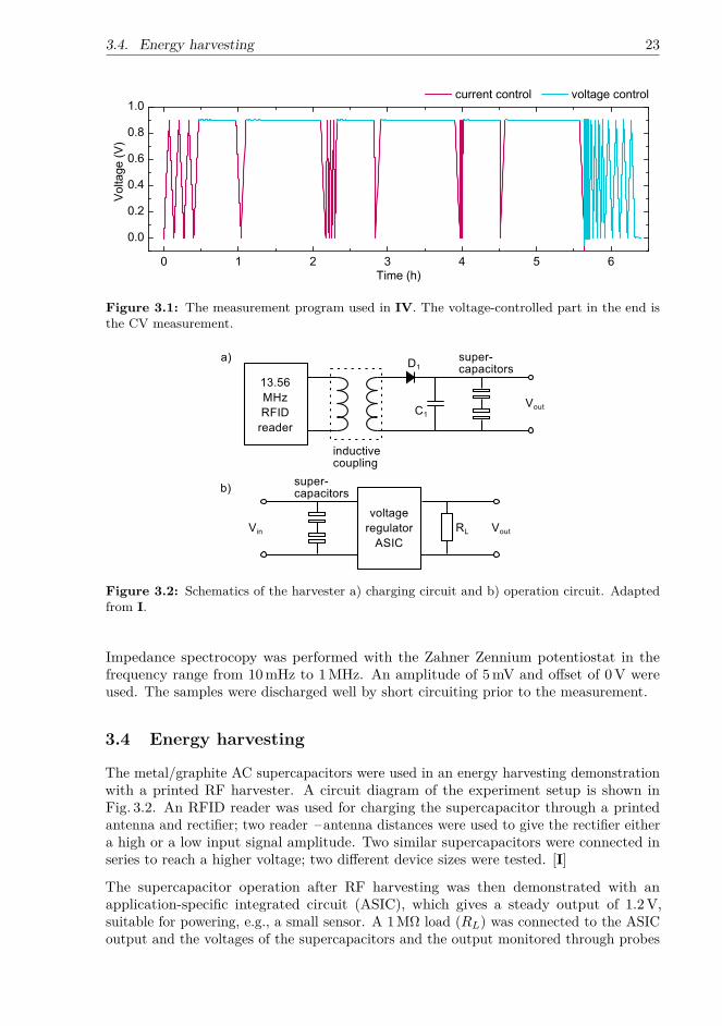
Figure 3.3: a) A photograph and b) a circuit schematic of the OPV/ECD harvester setup.Adapted from III.
with high input impedance. [I]
A PEDOT/rGO supercapacitor was used in another energy harvesting demonstration;here, a gravure-printed organic photovoltaic (OPV) module, provided by VTT (Oulu,Finland) [72], was used to charge the supercapacitor in ambient indoor lighting (Fig. 3.3).After charging, the supercapacitor was disconnected from the OPV module and used toswitch a small electrochromic display (ECD), provided by Acreo (Sweden), on and offrepeatedly by reversing the lead contacts every two seconds. [III]
4 Results and discussion
4.1 Activated carbon supercapacitors
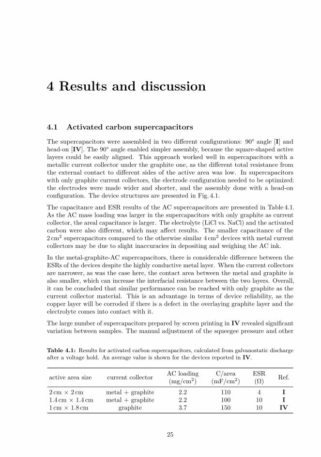
The supercapacitors were assembled in two different configurations: 90° angle [I] andhead-on [IV]. The 90° angle enabled simpler assembly, because the square-shaped activelayers could be easily aligned. This approach worked well in supercapacitors with ametallic current collector under the graphite one, as the different total resistance fromthe external contact to different sides of the active area was low. In supercapacitorswith only graphite current collectors, the electrode configuration needed to be optimized:the electrodes were made wider and shorter, and the assembly done with a head-onconfiguration. The device structures are presented in Fig. 4.1.
The capacitance and ESR results of the AC supercapacitors are presented in Table 4.1.As the AC mass loading was larger in the supercapacitors with only graphite as currentcollector, the areal capacitance is larger. The electrolyte (LiCl vs. NaCl) and the activatedcarbon were also different, which may affect results. The smaller capacitance of the2 cm2 supercapacitors compared to the otherwise similar 4 cm2 devices with metal currentcollectors may be due to slight inaccuracies in depositing and weighing the AC ink.
In the metal-graphite-AC supercapacitors, there is considerable difference between theESRs of the devices despite the highly conductive metal layer. When the current collectorsare narrower, as was the case here, the contact area between the metal and graphite isalso smaller, which can increase the interfacial resistance between the two layers. Overall,it can be concluded that similar performance can be reached with only graphite as thecurrent collector material. This is an advantage in terms of device reliability, as thecopper layer will be corroded if there is a defect in the overlaying graphite layer and theelectrolyte comes into contact with it.
The large number of supercapacitors prepared by screen printing in IV revealed significantvariation between samples. The manual adjustment of the squeegee pressure and other
Table 4.1: Results for activated carbon supercapacitors, calculated from galvanostatic dischargeafter a voltage hold. An average value is shown for the devices reported in IV.
active area size current collector AC loading C/area ESR Ref.(mg/cm2) (mF/cm2) (Ω)2 cm × 2 cm metal + graphite 2.2 110 4 I1.4 cm × 1.4 cm metal + graphite 2.2 100 10 I1 cm × 1.8 cm graphite 3.7 150 10 IV
25
26 Chapter 4. Results and discussion
Figure 4.1: a) Schematic of the supercapacitor assembly. The copper layer was used in I butnot in IV. b) Printed electrodes on graphite current collectors. c) A supercapacitor sample withmetal and graphite current collectors, assembled in 90° angle. d) A supercapacitor with onlygraphite current collectors, assembled with head-on conguration. Figures a and c adapted fromI, b and d from IV.
parameters – such as screen height and squeegee speed – resulted in different layerthicknesses produced on different fabrication times. The differences could have beenavoided by printing many more samples than needed, measuring, e.g., the sheet resistancesof the graphite, and selecting only the ones with similar resistance to be used in devices.However, the use of different electrodes, both in terms of graphite layer conductivity andAC layer mass loading, enables examination of the dependence between the parametersas well as optimization of the devices.
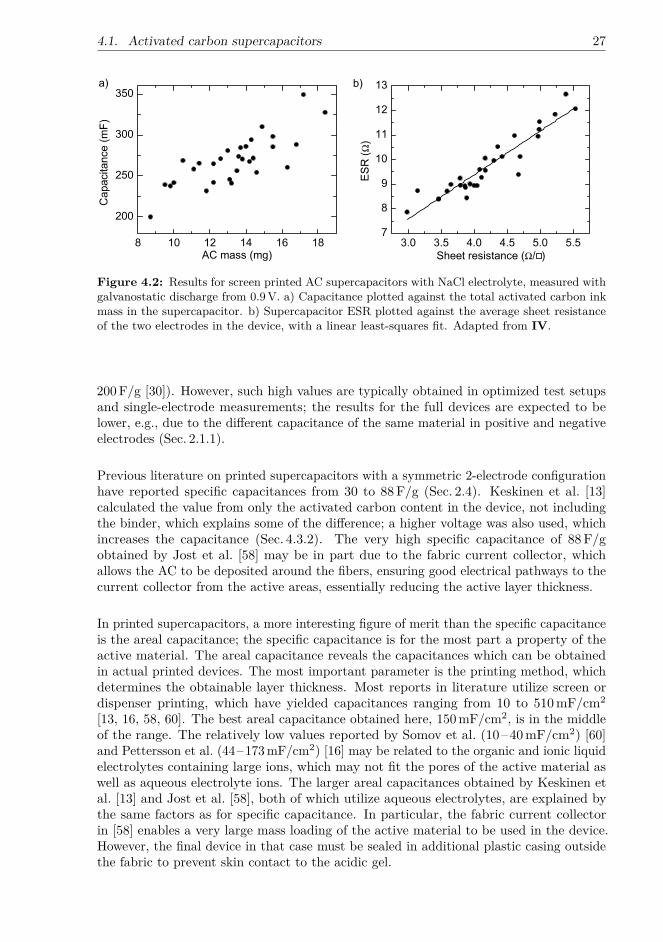
The correlation between capacitance and AC mass is not very good (Fig. 4.2a), despitethe straightforward theoretical correspondence between the two. One possible cause isinaccuracy in weighing the AC layer; the small amount of material added on a relativelylarge sheet of plastic is difficult to weigh reliably. Another is the amount of AC materialwhich is actually taking part in the charge storage: poor contact to the current collectoror incomplete access of the electrolyte can render the AC material inactive. The formerwas investigated in IV through a pressing test, where the AC layers were pressed afterprinting to ensure good contact between the particles, similarly to the fabrication ofpressed active material pellets in many studies on new supercapacitor materials. However,no difference was found to the samples with unpressed electrodes.
The specific capacitance, calculated from the total AC ink dry mass including binder,ranged from 16F/g to 26F/g. It decreased with increasing AC mass, even though the masswas on the order of that recommended by Stoller and Ruoff [48]. The dependence shouldbe taken into account when designing devices of a given capacitance for applications.The average value, 20F/g, corresponds to the single-electrode value of 80F/g, whichis much lower than the highest reported literature values for activated carbon (up to
4.1. Activated carbon supercapacitors 27
Figure 4.2: Results for screen printed AC supercapacitors with NaCl electrolyte, measured withgalvanostatic discharge from 0.9V. a) Capacitance plotted against the total activated carbon inkmass in the supercapacitor. b) Supercapacitor ESR plotted against the average sheet resistanceof the two electrodes in the device, with a linear least-squares fit. Adapted from IV.
200F/g [30]). However, such high values are typically obtained in optimized test setupsand single-electrode measurements; the results for the full devices are expected to belower, e.g., due to the different capacitance of the same material in positive and negativeelectrodes (Sec. 2.1.1).
Previous literature on printed supercapacitors with a symmetric 2-electrode configurationhave reported specific capacitances from 30 to 88F/g (Sec. 2.4). Keskinen et al. [13]calculated the value from only the activated carbon content in the device, not includingthe binder, which explains some of the difference; a higher voltage was also used, whichincreases the capacitance (Sec. 4.3.2). The very high specific capacitance of 88F/gobtained by Jost et al. [58] may be in part due to the fabric current collector, whichallows the AC to be deposited around the fibers, ensuring good electrical pathways to thecurrent collector from the active areas, essentially reducing the active layer thickness.
In printed supercapacitors, a more interesting figure of merit than the specific capacitanceis the areal capacitance; the specific capacitance is for the most part a property of theactive material. The areal capacitance reveals the capacitances which can be obtainedin actual printed devices. The most important parameter is the printing method, whichdetermines the obtainable layer thickness. Most reports in literature utilize screen ordispenser printing, which have yielded capacitances ranging from 10 to 510mF/cm2
[13, 16, 58, 60]. The best areal capacitance obtained here, 150mF/cm2, is in the middleof the range. The relatively low values reported by Somov et al. (10–40mF/cm2) [60]and Pettersson et al. (44–173mF/cm2) [16] may be related to the organic and ionic liquidelectrolytes containing large ions, which may not fit the pores of the active material aswell as aqueous electrolyte ions. The larger areal capacitances obtained by Keskinen etal. [13] and Jost et al. [58], both of which utilize aqueous electrolytes, are explained bythe same factors as for specific capacitance. In particular, the fabric current collectorin [58] enables a very large mass loading of the active material to be used in the device.However, the final device in that case must be sealed in additional plastic casing outsidethe fabric to prevent skin contact to the acidic gel.
28 Chapter 4. Results and discussion
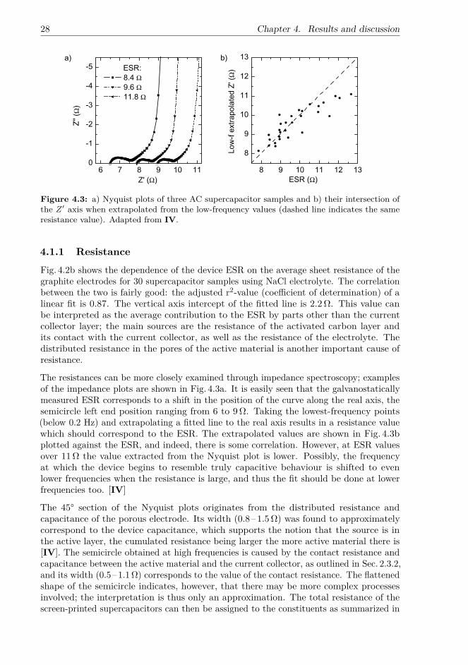
Figure 4.3: a) Nyquist plots of three AC supercapacitor samples and b) their intersection ofthe Z′ axis when extrapolated from the low-frequency values (dashed line indicates the sameresistance value). Adapted from IV.
4.1.1 Resistance
Fig. 4.2b shows the dependence of the device ESR on the average sheet resistance of thegraphite electrodes for 30 supercapacitor samples using NaCl electrolyte. The correlationbetween the two is fairly good: the adjusted r2-value (coefficient of determination) of alinear fit is 0.87. The vertical axis intercept of the fitted line is 2.2Ω. This value canbe interpreted as the average contribution to the ESR by parts other than the currentcollector layer; the main sources are the resistance of the activated carbon layer andits contact with the current collector, as well as the resistance of the electrolyte. Thedistributed resistance in the pores of the active material is another important cause ofresistance.
The resistances can be more closely examined through impedance spectroscopy; examplesof the impedance plots are shown in Fig. 4.3a. It is easily seen that the galvanostaticallymeasured ESR corresponds to a shift in the position of the curve along the real axis, thesemicircle left end position ranging from 6 to 9Ω. Taking the lowest-frequency points(below 0.2 Hz) and extrapolating a fitted line to the real axis results in a resistance valuewhich should correspond to the ESR. The extrapolated values are shown in Fig. 4.3bplotted against the ESR, and indeed, there is some correlation. However, at ESR valuesover 11Ω the value extracted from the Nyquist plot is lower. Possibly, the frequencyat which the device begins to resemble truly capacitive behaviour is shifted to evenlower frequencies when the resistance is large, and thus the fit should be done at lowerfrequencies too. [IV]
The 45° section of the Nyquist plots originates from the distributed resistance andcapacitance of the porous electrode. Its width (0.8–1.5Ω) was found to approximatelycorrespond to the device capacitance, which supports the notion that the source is inthe active layer, the cumulated resistance being larger the more active material there is[IV]. The semicircle obtained at high frequencies is caused by the contact resistance andcapacitance between the active material and the current collector, as outlined in Sec. 2.3.2,and its width (0.5–1.1Ω) corresponds to the value of the contact resistance. The flattenedshape of the semicircle indicates, however, that there may be more complex processesinvolved; the interpretation is thus only an approximation. The total resistance of thescreen-printed supercapacitors can then be assigned to the constituents as summarized in
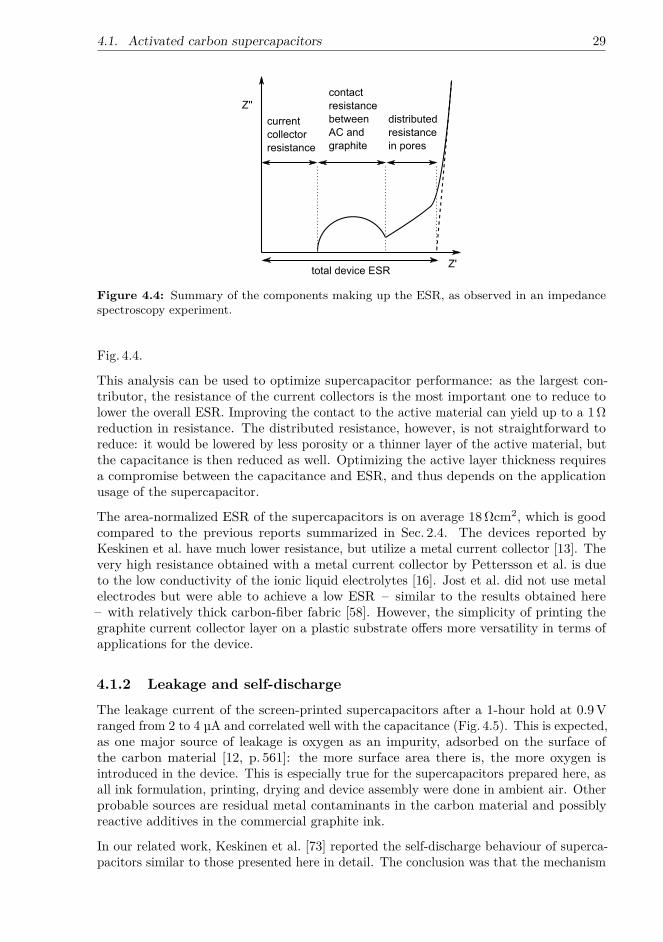
4.1. Activated carbon supercapacitors 29
Figure 4.4: Summary of the components making up the ESR, as observed in an impedancespectroscopy experiment.
Fig. 4.4.
This analysis can be used to optimize supercapacitor performance: as the largest con-tributor, the resistance of the current collectors is the most important one to reduce tolower the overall ESR. Improving the contact to the active material can yield up to a 1Ωreduction in resistance. The distributed resistance, however, is not straightforward toreduce: it would be lowered by less porosity or a thinner layer of the active material, butthe capacitance is then reduced as well. Optimizing the active layer thickness requiresa compromise between the capacitance and ESR, and thus depends on the applicationusage of the supercapacitor.
The area-normalized ESR of the supercapacitors is on average 18Ωcm2, which is goodcompared to the previous reports summarized in Sec. 2.4. The devices reported byKeskinen et al. have much lower resistance, but utilize a metal current collector [13]. Thevery high resistance obtained with a metal current collector by Pettersson et al. is dueto the low conductivity of the ionic liquid electrolytes [16]. Jost et al. did not use metalelectrodes but were able to achieve a low ESR – similar to the results obtained here– with relatively thick carbon-fiber fabric [58]. However, the simplicity of printing thegraphite current collector layer on a plastic substrate offers more versatility in terms ofapplications for the device.
4.1.2 Leakage and self-dischargeThe leakage current of the screen-printed supercapacitors after a 1-hour hold at 0.9Vranged from 2 to 4 µA and correlated well with the capacitance (Fig. 4.5). This is expected,as one major source of leakage is oxygen as an impurity, adsorbed on the surface ofthe carbon material [12, p. 561]: the more surface area there is, the more oxygen isintroduced in the device. This is especially true for the supercapacitors prepared here, asall ink formulation, printing, drying and device assembly were done in ambient air. Otherprobable sources are residual metal contaminants in the carbon material and possiblyreactive additives in the commercial graphite ink.
In our related work, Keskinen et al. [73] reported the self-discharge behaviour of superca-pacitors similar to those presented here in detail. The conclusion was that the mechanism
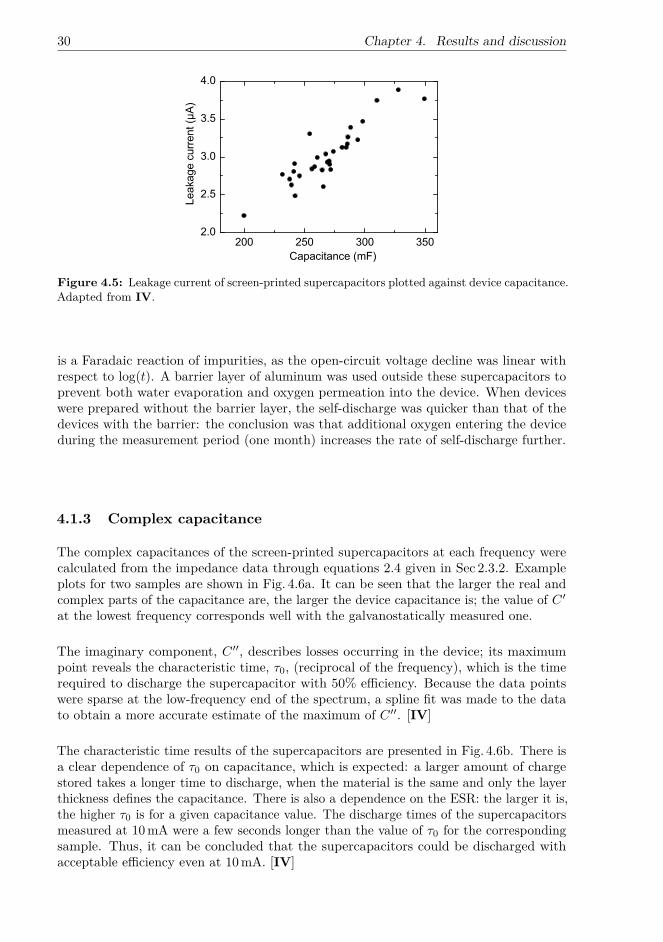
30 Chapter 4. Results and discussion
2 0 0 2 5 0 3 0 0 3 5 02 . 0
2 . 5
3 . 0
3 . 5
4 . 0
C a p a c i t a n c e ( m F )Figure 4.5: Leakage current of screen-printed supercapacitors plotted against device capacitance.Adapted from IV.
is a Faradaic reaction of impurities, as the open-circuit voltage decline was linear withrespect to log(t). A barrier layer of aluminum was used outside these supercapacitors toprevent both water evaporation and oxygen permeation into the device. When deviceswere prepared without the barrier layer, the self-discharge was quicker than that of thedevices with the barrier: the conclusion was that additional oxygen entering the deviceduring the measurement period (one month) increases the rate of self-discharge further.
4.1.3 Complex capacitance
The complex capacitances of the screen-printed supercapacitors at each frequency werecalculated from the impedance data through equations 2.4 given in Sec 2.3.2. Exampleplots for two samples are shown in Fig. 4.6a. It can be seen that the larger the real andcomplex parts of the capacitance are, the larger the device capacitance is; the value of C ′at the lowest frequency corresponds well with the galvanostatically measured one.
The imaginary component, C ′′, describes losses occurring in the device; its maximumpoint reveals the characteristic time, τ0, (reciprocal of the frequency), which is the timerequired to discharge the supercapacitor with 50% efficiency. Because the data pointswere sparse at the low-frequency end of the spectrum, a spline fit was made to the datato obtain a more accurate estimate of the maximum of C ′′. [IV]
The characteristic time results of the supercapacitors are presented in Fig. 4.6b. There isa clear dependence of τ0 on capacitance, which is expected: a larger amount of chargestored takes a longer time to discharge, when the material is the same and only the layerthickness defines the capacitance. There is also a dependence on the ESR: the larger it is,the higher τ0 is for a given capacitance value. The discharge times of the supercapacitorsmeasured at 10mA were a few seconds longer than the value of τ0 for the correspondingsample. Thus, it can be concluded that the supercapacitors could be discharged withacceptable efficiency even at 10mA. [IV]
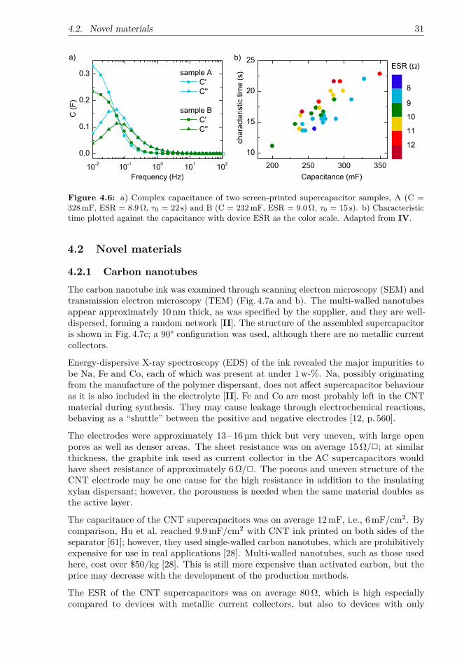
4.2. Novel materials 31
Figure 4.6: a) Complex capacitance of two screen-printed supercapacitor samples, A (C =328mF, ESR = 8.9Ω, τ0 = 22 s) and B (C = 232mF, ESR = 9.0Ω, τ0 = 15 s). b) Characteristictime plotted against the capacitance with device ESR as the color scale. Adapted from IV.
4.2 Novel materials
4.2.1 Carbon nanotubesThe carbon nanotube ink was examined through scanning electron microscopy (SEM) andtransmission electron microscopy (TEM) (Fig. 4.7a and b). The multi-walled nanotubesappear approximately 10 nm thick, as was specified by the supplier, and they are well-dispersed, forming a random network [II]. The structure of the assembled supercapacitoris shown in Fig. 4.7c; a 90° configuration was used, although there are no metallic currentcollectors.
Energy-dispersive X-ray spectroscopy (EDS) of the ink revealed the major impurities tobe Na, Fe and Co, each of which was present at under 1w-%. Na, possibly originatingfrom the manufacture of the polymer dispersant, does not affect supercapacitor behaviouras it is also included in the electrolyte [II]. Fe and Co are most probably left in the CNTmaterial during synthesis. They may cause leakage through electrochemical reactions,behaving as a “shuttle” between the positive and negative electrodes [12, p. 560].
The electrodes were approximately 13–16µm thick but very uneven, with large openpores as well as denser areas. The sheet resistance was on average 15Ω/2; at similarthickness, the graphite ink used as current collector in the AC supercapacitors wouldhave sheet resistance of approximately 6Ω/2. The porous and uneven structure of theCNT electrode may be one cause for the high resistance in addition to the insulatingxylan dispersant; however, the porousness is needed when the same material doubles asthe active layer.
The capacitance of the CNT supercapacitors was on average 12mF, i.e., 6mF/cm2. Bycomparison, Hu et al. reached 9.9mF/cm2 with CNT ink printed on both sides of theseparator [61]; however, they used single-walled carbon nanotubes, which are prohibitivelyexpensive for use in real applications [28]. Multi-walled nanotubes, such as those usedhere, cost over $50/kg [28]. This is still more expensive than activated carbon, but theprice may decrease with the development of the production methods.
The ESR of the CNT supercapacitors was on average 80Ω, which is high especiallycompared to devices with metallic current collectors, but also to devices with only
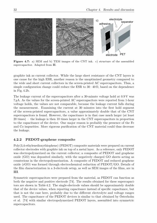
32 Chapter 4. Results and discussion
Figure 4.7: a) SEM and b) TEM images of the CNT ink. c) structure of the assembledsupercapacitor. Adapted from II.
graphite ink as current collector. While the large sheet resistance of the CNT layers isone cause for the high ESR, another reason is the unoptimized geometry compared tothe wide and short current collectors in the screen-printed AC supercapacitors. Thus, asimple configuration change could reduce the ESR to 30–40Ω, based on the dependencein Fig. 4.2b.
The leakage current of the supercapacitors after a 30-minute voltage hold at 0.9V was7 µA. As the values for the screen-printed AC supercapacitors were reported from 1-hourvoltage holds, the values are not comparable, because the leakage current falls duringthe measurement. Examining the current at 30 minutes into the first hold segmentof the screen-printed supercapacitors, a value approximately double that of the CNTsupercapacitors is found. However, the capacitance is in that case much larger (at least20 times) – the leakage is then 10 times larger in the CNT supercapacitors in proportionto the capacitance of the device. One major reason is probably the presence of the Feand Co impurities. More rigorous purification of the CNT material could thus decreasethe leakage.
4.2.2 PEDOT-graphene compositePoly(3,4-ethylenedioxythiophene) (PEDOT) composite materials were prepared on currentcollector electrodes with graphite ink on top of a metal layer. As a reference, only PEDOTwas electropolymerized on the current collector; a composite of PEDOT and grapheneoxide (GO) was deposited similarly, with the negatively charged GO sheets acting ascounterions in the electropolymerization. A composite of PEDOT and reduced grapheneoxide (rGO) was formed through electrochemical reduction of PEDOT/GO. Details ofthe film characterization in a 3-electrode setup, as well as SEM images of the films, are inIII.
Symmetric supercapacitors were prepared from the material, as PEDOT can function asboth the negative and positive electrode [74]. The results obtained for these supercapaci-tors are shown in Table 4.2. The single-electrode values should be approximately doublethat of the device values, when reporting capacitance instead of specific capacitance, butthat is not the case here, probably due to the different electrolyte and voltage rangesused. The capacitance of the PEDOT devices is similar to that obtained by Österholmet al. [74] with similar electropolymerized PEDOT layers, assembled into symmetricsupercapacitors.
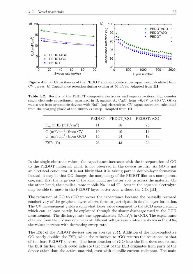
4.2. Novel materials 33
0 2 0 4 0 6 0 8 0 1 0 00
5
1 0
1 5
2 0
0 5 0 0 1 0 0 0 1 5 0 0 2 0 0 09 5
9 6
9 7
9 8
9 9
1 0 0C/A
(mF/c
m2 )
S w e e p r a t e ( m V / s )
P E D O T / r G O P E D O T / G O P E D O T
b ) P E D O T / r G O P E D O T / G O P E D O T
Capa
citanc
e rete
ntion
(%)
C y c l e n u m b e r
a )
Figure 4.8: a) Capacitances of the PEDOT and composite supercapacitors, calculated fromCV curves. b) Capacitance retention during cycling at 50 mV/s. Adapted from III.
Table 4.2: Results of the PEDOT composite electrodes and supercapacitors. Cse denotessingle-electrode capacitance, measured in IL against Ag/AgCl from –0.4V to +0.8V. Othervalues are from symmetric devices with NaCl (aq) electrolyte. CV capacitances are calculatedfrom the charging phase of the 100mV/s sweep. Adapted from III.
PEDOT PEDOT/GO PEDOT/rGOCse in IL (mF/cm2) 11 16 25C (mF/cm2) from CV 10 10 14C (mF/cm2) from GCD 14 14 18ESR (Ω) 26 43 25
In the single-electrode values, the capacitance increases with the incorporation of GOto the PEDOT material, which is not observed in the device results. As GO is notan electrical conductor, it is not likely that it is taking part in double-layer formation.Instead, it may be that GO changes the morphology of the PEDOT film to a more porousone, such that the large ions of the ionic liquid are better able to access the material. Onthe other hand, the smaller, more mobile Na+ and Cl− ions in the aqueous electrolytemay be able to move in the PEDOT layer better even without the GO. [III]
The reduction of GO to rGO improves the capacitance because the partially restoredconductivity of the graphene layers allows them to participate in double-layer formation.The CV measurement yields a somewhat lower value compared to the GCD measurement,which can, at least partly, be explained through the slower discharge used in the GCDmeasurement. The discharge rate was approximately 3.5mV/s in GCD. The capacitanceobtained from the CV measurements at different voltage sweep rates are shown in Fig. 4.8a;the values increase with decreasing sweep rate.
The ESR of the PEDOT devices was on average 26Ω. Addition of the non-conductiveGO nearly doubles the ESR, while the reduction to rGO returns the resistance to thatof the bare PEDOT devices. The incorporation of rGO into the film does not reducethe ESR further, which could indicate that most of the ESR originates from parts of thedevice other than the active material, even with metallic current collectors. The main
34 Chapter 4. Results and discussion
benefit of rGO is then the approximately 30% increase in capacitance compared to barePEDOT, due to the added surface area capable of double-layer formation. [III]
The cycling stability of the devices is fairly good with 5–7% drop in capacitance after 2000cycles at 50mV/s, calculated from GCD before and after the cycling. The evolution of thecapacitance during cycling, calculated from the CV curves, is shown in Fig. 4.8b. Thereare no significant differences between the sample types; PEDOT/GO yields the lowestcapacitance drop after the cycling. It is possible that some electrochemical reduction ofthe GO to rGO takes place during the cycling as well as during the 30-minute voltagehold prior to the galvanostatic discharge. The difference is, however, too small to makea definitive conclusion. In general, the cycling stability of conducting polymers is lowerin aqueous electrolytes than in ionic liquids [35], which explains the better stability ofsimilar devices with ionic liquid electrolyte [74]. However, using aqueous electrolytesbrings the advantages of facile processing and use of the devices.
4.3 Measurement parameter effects
4.3.1 Rate dependenceMany factors can influence the results of supercapacitor measurements; one such effectis seen in Fig. 4.8a, where a slower CV sweep rate produces a higher capacitance. Onecause for this is the different migration time of the electrolyte ions in the pores of theelectrode – with a slower rate, the full surface area of the active material is in use. Withpseudocapacitive materials, the reaction time scale may also cause some delay in theresponse of the device. Similarly to CV, a lower measurement current in GCD shouldalso yield a higher capacitance, and this is frequently observed [75].
In II, lower measurement current did not yield a higher capacitance, but in fact a lowerone. The effect was studied with a simple circuit model, where the supercapacitor wasrepresented by a capacitor, a series resistor and a parallel leakage resistance of 130 kΩ(Fig. 4.9a). The leakage resistance was determined from the value of the measured leakagecurrent at 0.9V. A simulation with a 30-minute voltage hold and a discharge at constantcurrent was run, and the resulting discharge curve used for capacitance calculationsimilarly to measured results. The capacitances at different currents, both measured andsimulated, are shown in Fig. 4.9b.
Stoller and Ruoff [48] note that when the measurement current is on the order of theleakage current, the latter may interfere with the results. This is indeed observed here, asthe apparent capacitance begins to fall when the measurement current is approximatelythree times the leakage current (7µA) at 0.9V. In reality, the leakage “resistance” isvoltage-dependent, with a higher resistance at lower voltages due to the likely Faradaicorigin of the leakage. Yet, even a very simple model such as the one used here yieldsresults close to the measured data.
4.3.2 Maximum voltageThe operating voltage of a supercapacitor is a very important parameter which affectsthe performance of the device. Screen-printed AC supercapacitors were used in testingthe effect of the voltage on the capacitance and the leakage current [IV]. In an initialtest, the same device was charged to different maximum voltages from 0.8V to 1.2V andthe capacitance calculated from GCD after a 30-minute hold at the respective voltages.
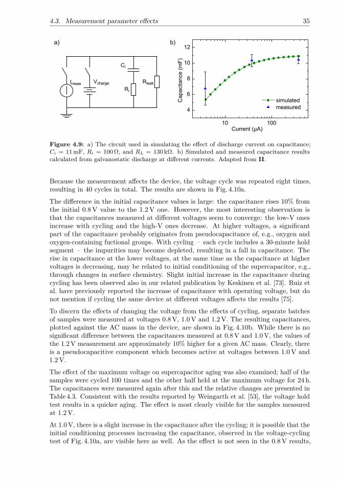
4.3. Measurement parameter effects 35
Figure 4.9: a) The circuit used in simulating the effect of discharge current on capacitance;Ci = 11mF, Ri = 100Ω, and RL = 130 kΩ. b) Simulated and measured capacitance resultscalculated from galvanostatic discharge at different currents. Adapted from II.
Because the measurement affects the device, the voltage cycle was repeated eight times,resulting in 40 cycles in total. The results are shown in Fig. 4.10a.
The difference in the initial capacitance values is large: the capacitance rises 10% fromthe initial 0.8V value to the 1.2V one. However, the most interesting observation isthat the capacitances measured at different voltages seem to converge: the low-V onesincrease with cycling and the high-V ones decrease. At higher voltages, a significantpart of the capacitance probably originates from pseudocapacitance of, e.g., oxygen andoxygen-containing fuctional groups. With cycling – each cycle includes a 30-minute holdsegment – the impurities may become depleted, resulting in a fall in capacitance. Therise in capacitance at the lower voltages, at the same time as the capacitance at highervoltages is decreasing, may be related to initial conditioning of the supercapacitor, e.g.,through changes in surface chemistry. Slight initial increase in the capacitance duringcycling has been observed also in our related publication by Keskinen et al. [73]. Ruiz etal. have previously reported the increase of capacitance with operating voltage, but donot mention if cycling the same device at different voltages affects the results [75].
To discern the effects of changing the voltage from the effects of cycling, separate batchesof samples were measured at voltages 0.8V, 1.0V and 1.2V. The resulting capacitances,plotted against the AC mass in the device, are shown in Fig. 4.10b. While there is nosignificant difference between the capacitances measured at 0.8V and 1.0V, the values ofthe 1.2V measurement are approximately 10% higher for a given AC mass. Clearly, thereis a pseudocapacitive component which becomes active at voltages between 1.0V and1.2V.
The effect of the maximum voltage on supercapacitor aging was also examined; half of thesamples were cycled 100 times and the other half held at the maximum voltage for 24 h.The capacitances were measured again after this and the relative changes are presented inTable 4.3. Consistent with the results reported by Weingarth et al. [53], the voltage holdtest results in a quicker aging. The effect is most clearly visible for the samples measuredat 1.2V.
At 1.0V, there is a slight increase in the capacitance after the cycling; it is possible that theinitial conditioning processes increasing the capacitance, observed in the voltage-cyclingtest of Fig. 4.10a, are visible here as well. As the effect is not seen in the 0.8V results,
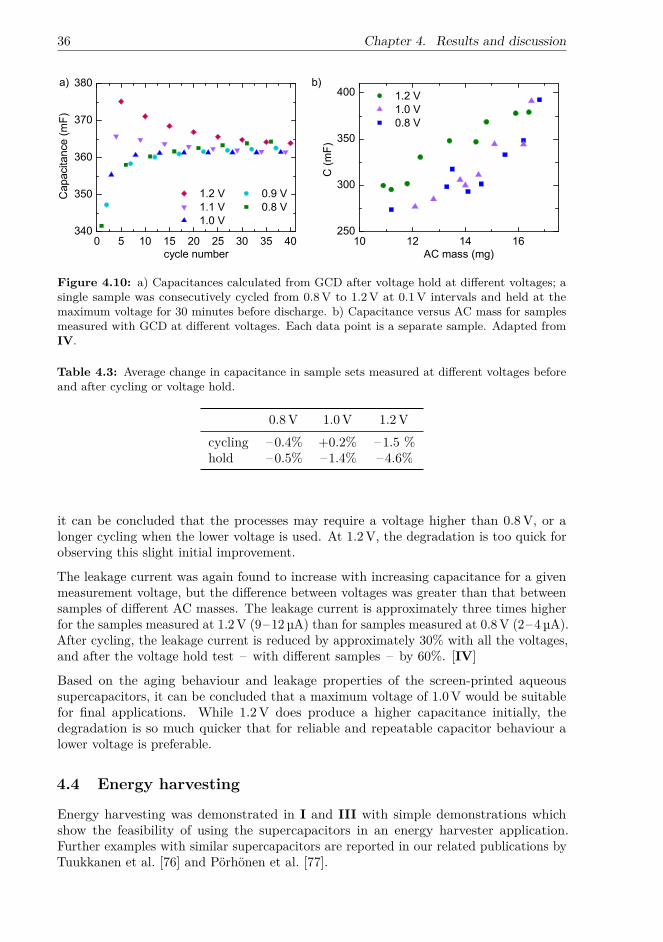
36 Chapter 4. Results and discussion
1 0 1 2 1 4 1 62 5 0
3 0 0
3 5 0
4 0 0
0 5 1 0 1 5 2 0 2 5 3 0 3 5 4 03 4 0
3 5 0
3 6 0
3 7 0
3 8 0 1 . 2 V 1 . 0 V 0 . 8 V
C (mF
)
A C m a s s ( m g )
b )
1 . 2 V 0 . 9 V 1 . 1 V 0 . 8 V 1 . 0 V
Capa
citanc
e (mF
)
c y c l e n u m b e r
a )
Figure 4.10: a) Capacitances calculated from GCD after voltage hold at different voltages; asingle sample was consecutively cycled from 0.8V to 1.2V at 0.1V intervals and held at themaximum voltage for 30 minutes before discharge. b) Capacitance versus AC mass for samplesmeasured with GCD at different voltages. Each data point is a separate sample. Adapted fromIV.
Table 4.3: Average change in capacitance in sample sets measured at different voltages beforeand after cycling or voltage hold.
0.8V 1.0V 1.2Vcycling –0.4% +0.2% –1.5 %hold –0.5% –1.4% –4.6%
it can be concluded that the processes may require a voltage higher than 0.8V, or alonger cycling when the lower voltage is used. At 1.2V, the degradation is too quick forobserving this slight initial improvement.
The leakage current was again found to increase with increasing capacitance for a givenmeasurement voltage, but the difference between voltages was greater than that betweensamples of different AC masses. The leakage current is approximately three times higherfor the samples measured at 1.2V (9–12µA) than for samples measured at 0.8V (2–4µA).After cycling, the leakage current is reduced by approximately 30% with all the voltages,and after the voltage hold test – with different samples – by 60%. [IV]
Based on the aging behaviour and leakage properties of the screen-printed aqueoussupercapacitors, it can be concluded that a maximum voltage of 1.0V would be suitablefor final applications. While 1.2V does produce a higher capacitance initially, thedegradation is so much quicker that for reliable and repeatable capacitor behaviour alower voltage is preferable.
4.4 Energy harvesting
Energy harvesting was demonstrated in I and III with simple demonstrations whichshow the feasibility of using the supercapacitors in an energy harvester application.Further examples with similar supercapacitors are reported in our related publications byTuukkanen et al. [76] and Pörhönen et al. [77].
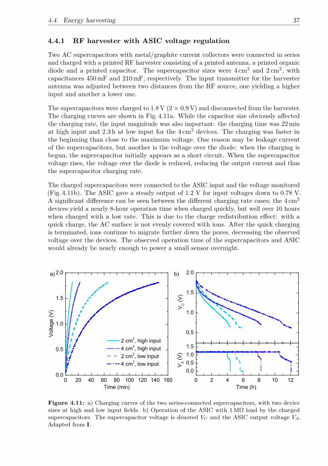
4.4. Energy harvesting 37
4.4.1 RF harvester with ASIC voltage regulation
Two AC supercapacitors with metal/graphite current collectors were connected in seriesand charged with a printed RF harvester consisting of a printed antenna, a printed organicdiode and a printed capacitor. The supercapacitor sizes were 4 cm2 and 2 cm2, withcapacitances 450mF and 210mF, respectively. The input transmitter for the harvesterantenna was adjusted between two distances from the RF source, one yielding a higherinput and another a lower one.
The supercapacitors were charged to 1.8V (2 × 0.9V) and disconnected from the harvester.The charging curves are shown in Fig. 4.11a. While the capacitor size obviously affectedthe charging rate, the input magnitude was also important: the charging time was 22minat high input and 2.3 h at low input for the 4 cm2 devices. The charging was faster inthe beginning than close to the maximum voltage. One reason may be leakage currentof the supercapacitors, but another is the voltage over the diode: when the charging isbegun, the supercapacitor initially appears as a short circuit. When the supercapacitorvoltage rises, the voltage over the diode is reduced, reducing the output current and thusthe supercapacitor charging rate.
The charged supercapacitors were connected to the ASIC input and the voltage monitored(Fig. 4.11b). The ASIC gave a steady output of 1.2 V for input voltages down to 0.78 V.A significant difference can be seen between the different charging rate cases; the 4 cm2
devices yield a nearly 8-hour operation time when charged quickly, but well over 10 hourswhen charged with a low rate. This is due to the charge redistribution effect: with aquick charge, the AC surface is not evenly covered with ions. After the quick chargingis terminated, ions continue to migrate further down the pores, decreasing the observedvoltage over the devices. The observed operation time of the supercapacitors and ASICwould already be nearly enough to power a small sensor overnight.
0 2 0 4 0 6 0 8 0 1 0 0 1 2 0 1 4 0 1 6 00 . 0
0 . 5
1 . 0
1 . 5
2 . 0
0 . 5
1 . 0
1 . 5
2 . 0
0 2 4 6 8 1 0 1 20 . 00 . 51 . 01 . 5
Volta
ge (V
)
T i m e ( m i n )
2 c m 2 , h i g h i n p u t 4 c m 2 , h i g h i n p u t 2 c m 2 , l o w i n p u t 4 c m 2 , l o w i n p u t
b )
V C (V)
a )
T i m e ( h )
V A (V)
Figure 4.11: a) Charging curves of the two series-connected supercapacitors, with two devicesizes at high and low input fields. b) Operation of the ASIC with 1MΩ load by the chargedsupercapacitors. The supercapacitor voltage is denoted VC and the ASIC output voltage VA.Adapted from I.
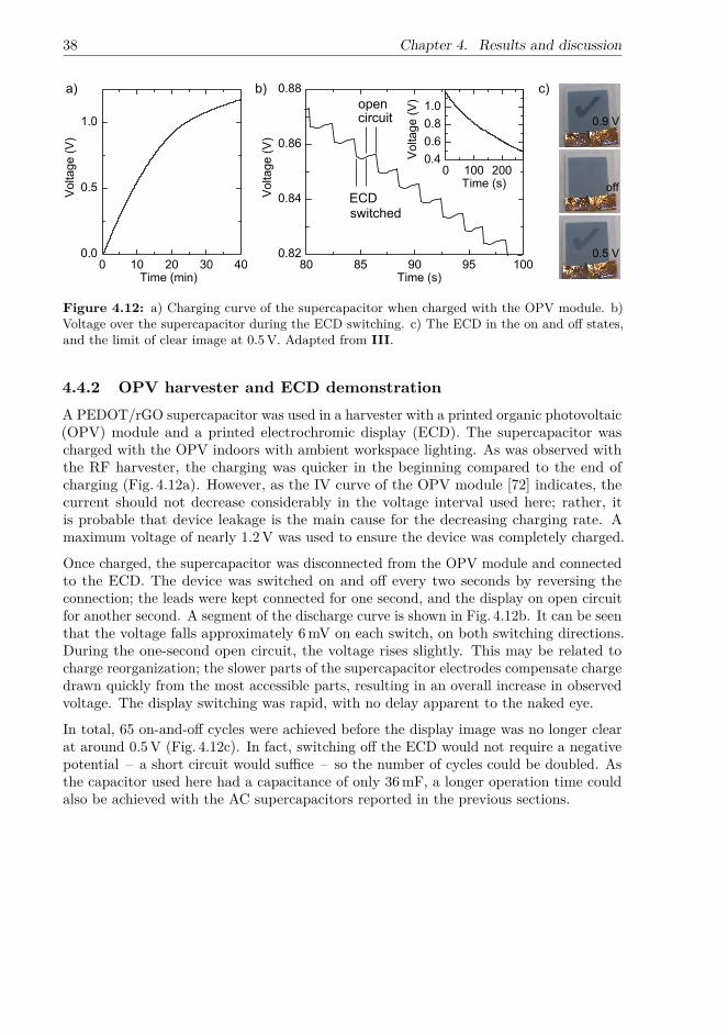
38 Chapter 4. Results and discussion
Figure 4.12: a) Charging curve of the supercapacitor when charged with the OPV module. b)Voltage over the supercapacitor during the ECD switching. c) The ECD in the on and off states,and the limit of clear image at 0.5V. Adapted from III.
4.4.2 OPV harvester and ECD demonstrationA PEDOT/rGO supercapacitor was used in a harvester with a printed organic photovoltaic(OPV) module and a printed electrochromic display (ECD). The supercapacitor wascharged with the OPV indoors with ambient workspace lighting. As was observed withthe RF harvester, the charging was quicker in the beginning compared to the end ofcharging (Fig. 4.12a). However, as the IV curve of the OPV module [72] indicates, thecurrent should not decrease considerably in the voltage interval used here; rather, itis probable that device leakage is the main cause for the decreasing charging rate. Amaximum voltage of nearly 1.2V was used to ensure the device was completely charged.
Once charged, the supercapacitor was disconnected from the OPV module and connectedto the ECD. The device was switched on and off every two seconds by reversing theconnection; the leads were kept connected for one second, and the display on open circuitfor another second. A segment of the discharge curve is shown in Fig. 4.12b. It can be seenthat the voltage falls approximately 6mV on each switch, on both switching directions.During the one-second open circuit, the voltage rises slightly. This may be related tocharge reorganization; the slower parts of the supercapacitor electrodes compensate chargedrawn quickly from the most accessible parts, resulting in an overall increase in observedvoltage. The display switching was rapid, with no delay apparent to the naked eye.
In total, 65 on-and-off cycles were achieved before the display image was no longer clearat around 0.5V (Fig. 4.12c). In fact, switching off the ECD would not require a negativepotential – a short circuit would suffice – so the number of cycles could be doubled. Asthe capacitor used here had a capacitance of only 36mF, a longer operation time couldalso be achieved with the AC supercapacitors reported in the previous sections.
5 Summary and outlook
The need for printable, low-cost energy storage solutions is growing due to the increase indistributed and ubiquitous electronics. Placing billions of sensors and other electronicdevices everywhere in our surroundings calls for an autonomous energy source, i.e.,harvesting the energy from the ambient environment. The supercapacitors presented inthis thesis offer an excellent option for the interim storage of the harvested energy: theyare cheap, printable, potentially flexible, and have a good cycling stability. The devicescan be safely placed in any environment as they have no toxic components, and they canbe disposed of, e.g., through incineration.
The thesis studied different types of printed and coated supercapacitors. Currently, theconventional activated carbon material yields the best results due to its highest perfor-mance as well as low cost. However, there are intensive efforts to develop nanostructuredmaterials which could surpass the performance of activated carbon. One such material iscarbon nanotubes, which not only have a high surface area, but also good conductivity. Itwas shown in this thesis that an ink formulated from CNTs can be used in supercapacitorelectrodes in such a way that it is the only electrode layer, doubling as both the currentcollector and the active material, which simplifies the fabrication process. The capacitancereached with the CNT supercapacitors was 6mF/cm2 and the ESR 80Ω. While not yetcompetetive with activated carbon, further developments in the synthesis, purificationand dispersion methods could produce better devices.
Another interesting direction of supercapacitor material development are composites ofconductive polymers, i.e., pseudocapacitive materials, and carbon nanomaterials. Anelectropolymerized composite, PEDOT and reduced graphene oxide, was studied in thisthesis. It was fabricated directly on the blade-coated current collector electrodes andused in a symmetric supercapacitor; the succesful scale-up of the electropolymerizationfrom the conventional millimetre-sized electrodes used in electropolymerization on print-able electrodes shows the potential of the method in larger-scale manufacturing. Thecapacitance was 18mF/cm2 and ESR 25Ω. The addition of the reduced graphene oxideimproved the capacitance 30% compared to that of devices prepared with only PEDOTlayers.
Screen-printed activated carbon based supercapacitors reached on average a capacitanceof 150mF/cm2 and ESR of 10Ω. In the short term, this material is the most interestingdirection for the development of printable supercapacitors. The properties were studiedin more detail over a large sample set with different layer thicknesses: it was found thatthe specific capacitance decreases somewhat with the activated carbon mass and that themagnitude of the leakage current is directly related to the capacitance. Current collectorsconsisting only of graphite ink were found to be the main source of the device ESR. Moredetailed analysis of the device resistances though impedance spectroscopy revealed the
39
40 Chapter 5. Summary and outlook
sources to be:
– resistance of the current collectors and bulk electrolyte: 6–9Ω,– contact resistance between the active material and the current collector: 0.5–1.1Ω
and– distributed resistance of the electrolyte and the active material in the porous
electrode: 0.8–1.5Ω.
The maximum voltage was found to have a great effect on the capacitance, leakage andthe device stability, with higher voltage yielding higher capacitance but also larger leakageand quicker device degradation. Based on the results, a suitable compromise for themaximum voltage is 1.0V.
Demonstrations of the supercapacitors in energy harvesting were carried out with bothRF and light harvesting, and the performance of the supercapacitors was found suitablefor powering a small electronic device such as an electrochromic display. An essentialpart of any harvester containing a supercapacitor is a voltage control circuit, which canproduce a steady output from a supercapacitor where the voltage declines linearly ondischarge. Over 10 hours of operation was demonstrated with an application-specificintegrated circuit.
Important issues which need to be addressed in the future are the flexibility and shelf-lifeof the printed supercapacitors. Packaging and sealing the supercapacitors with aqueouselectrolyte in such a way that the device does not dry out is crucial for long-term operation.The flexibility of the devices presents even more requirements for durable packaging.Another future challenge is decreasing the ESR of the devices; as was found in this thesis,this practically means improving the conductivity of the current collectors. A metal layeris problematic not only due to issues with disposability, but also due to the corrosionin the case of defects in the graphite layer. Using only graphite yields approximately10Ω device resistances, which may still be too high in applications with high peak powerdemand. Better inks could be found from commercial sources or fabricated in-house;for example, carbon nanotubes as ink additives could provide the needed increase inconductivity. Overall, while the basic structure of the supercapacitors has here beendemonstrated to work well, future development of the materials and packaging shouldimprove the usability in applications further.

Bibliography
[1] R. Vullers, R. van Schaijk, I. Doms, C. Van Hoof, and R. Mertens, “Micropowerenergy harvesting,” Solid-State Electron., vol. 53, no. 7, pp. 684–693, 2009.
[2] C. O. Mathuna, T. O’Donnell, R. V. Martinez-Catala, J. Rohan, and B. O’Flynn,“Energy scavenging for long-term deployable wireless sensor networks,” Talanta,vol. 75, no. 3, pp. 613–623, 2008.
[3] J. A. Stankovic, “Research directions for the Internet of Things,” IEEE InternetThings J., vol. 1, no. 1, pp. 3–9, 2014.
[4] H. Jayakumar, K. Lee, W. S. Lee, A. Raha, Y. Kim, and V. Raghunathan, “Poweringthe Internet of Things,” in Proc. 2014 International Symposium on Low PowerElectronics and Design. ACM, 2014, pp. 375–380.
[5] P. Kamalinejad, C. Mahapatra, Z. Sheng, S. Mirabbasi, V. C. Leung, and Y. L.Guan, “Wireless energy harvesting for the internet of things,” IEEE Commun. Mag.,vol. 53, no. 6, pp. 102–108, 2015.
[6] R. Want, K. I. Farkas, and C. Narayanaswami, “Guest editors’ introduction: Energyharvesting and conservation,” IEEE Pervasive Comput., vol. 4, no. 1, pp. 14–17,2005.
[7] J. A. Paradiso and T. Starner, “Energy scavenging for mobile and wireless electronics,”IEEE Pervasive Comput., vol. 4, no. 1, pp. 18–27, 2005.
[8] J. Gubbi, R. Buyya, S. Marusic, and M. Palaniswami, “Internet of Things (IoT):A vision, architectural elements, and future directions,” Future Gener. Comp. Sy.,vol. 29, no. 7, pp. 1645–1660, 2013.
[9] D. Miorandi, S. Sicari, F. De Pellegrini, and I. Chlamtac, “Internet of things: Vision,applications and research challenges,” Ad Hoc Networks, vol. 10, no. 7, pp. 1497–1516,2012.
[10] V. Raghunathan, S. Ganeriwal, and M. Srivastava, “Emerging techniques for longlived wireless sensor networks,” IEEE Commun. Mag., vol. 44, no. 4, pp. 108–114,2006.
[11] J. Wen, Y. Yu, and C. Chen, “A review on lithium-ion batteries safety issues: existingproblems and possible solutions,” Mater. Express, vol. 2, no. 3, pp. 197–212, 2012.
[12] B. E. Conway, Electrochemical Supercapacitors: Scientific Fundamentals and Tech-nological Applications. New York: Kluwer Academic / Plenum Publishers, 1999.
41
42 Bibliography
[13] J. Keskinen, E. Sivonen, S. Jussila, M. Bergelin, M. Johansson, A. Vaari, andM. Smolander, “Printed supercapacitors on paperboard substrate,” Electrochim.Acta, vol. 85, pp. 302–306, 2012.
[14] F. Gonzales, “Supercapacitor Technologies and Markets 2016-2026,” IDTechEx, Tech.Rep., 2016.
[15] M. Kaempgen, C. K. Chan, J. Ma, Y. Cui, and G. Gruner, “Printable thin filmsupercapacitors using single-walled carbon nanotubes,” Nano Lett., vol. 9, no. 5, pp.1872–1876, 2009.
[16] F. Pettersson, J. Keskinen, T. Remonen, L. Von Hertzen, E. Jansson, K. Tappura,Y. Zhang, C.-E. Wilén, and R. Österbacka, “Printed environmentally friendly super-capacitors with ionic liquid electrolytes on paper,” J. Power Sources, vol. 271, pp.298–304, 2014.
[17] V. L. Pushparaj, M. M. Shaijumon, A. Kumar, S. Murugesan, L. Ci, R. Vajtai, R. J.Linhardt, O. Nalamasu, and P. M. Ajayan, “Flexible energy storage devices based onnanocomposite paper,” P. Natl. Acad. Sci., vol. 104, no. 34, pp. 13 574–13 577, 2007.
[18] J. S. Sagu, N. York, D. Southee, and K. Wijayantha, “Printed electrodes for flexible,light-weight solid-state supercapacitors–a feasibility study,” Circuit World, vol. 41,no. 2, pp. 80–86, 2015.
[19] J. R. Miller, “Market and Applications of Electrochemical Capacitors,” in Superca-pacitors: Materials, Systems and Applications, F. Beguin, E. Frackowiak, and M. Lu,Eds. John Wiley & Sons, 2013.
[20] R. Kötz and M. Carlen, “Principles and applications of electrochemical capacitors,”Electrochim. Acta, vol. 45, no. 15-16, pp. 2483–2498, 2000.
[21] S. W. Donne, “General Principles of Electrochemistry,” in Supercapacitors: Materials,Systems and Applications, F. Beguin, E. Frackowiak, and M. Lu, Eds. John Wiley& Sons, 2013.
[22] W. G. Pell and B. E. Conway, “Peculiarities and requirements of asymmetric capacitordevices based on combination of capacitor and battery-type electrodes,” J. PowerSources, vol. 136, no. 2, pp. 334–345, 2004.
[23] H. A. Andreas, “Self-discharge in electrochemical capacitors: A perspective article,”J. Electrochem. Soc., vol. 162, no. 5, pp. A5047–A5053, 2015.
[24] R. De Levie, “On porous electrodes in electrolyte solutions: I. capacitance effects,”Electrochim. Acta, vol. 8, no. 10, pp. 751–780, 1963.
[25] J. Chmiola, G. Yushin, Y. Gogotsi, C. Portet, P. Simon, and P.-L. Taberna, “Anoma-lous increase in carbon capacitance at pore sizes less than 1 nanometer,” Science,vol. 313, no. 5794, pp. 1760–1763, 2006.
[26] G. V. Merrett and A. S. Weddell, “Supercapacitor leakage in energy-harvestingsensor nodes: Fact or fiction?” in Ninth International Conference on NetworkedSensing Systems (INSS). IEEE, 2012, pp. 1–5.
Bibliography 43
[27] P. J. Hall, M. Mirzaeian, S. I. Fletcher, F. B. Sillars, A. J. Rennie, G. O. Shitta-Bey,G. Wilson, A. Cruden, and R. Carter, “Energy storage in electrochemical capacitors:designing functional materials to improve performance,” Energy Environ. Sci., vol. 3,no. 9, pp. 1238–1251, 2010.
[28] L. Weinstein and R. Dash, “Supercapacitor carbons – have exotic carbons failed?”Mater. Today, vol. 16, no. 10, pp. 356–357, 2013.
[29] A. G. Pandolfo and A. F. Hollenkamp, “Carbon properties and their role in superca-pacitors,” J. Power Sources, vol. 157, no. 1, pp. 11–27, 2006.
[30] P. Simon and Y. Gogotsi, “Materials for electrochemical capacitors,” Nat. Mater.,vol. 7, no. 11, pp. 845–854, 2008.
[31] X. Du, P. Guo, H. Song, and X. Chen, “Graphene nanosheets as electrode material forelectric double-layer capacitors,” Electrochim. Acta, vol. 55, no. 16, pp. 4812–4819,2010.
[32] D. R. Dreyer, S. Park, C. W. Bielawski, and R. S. Ruoff, “The chemistry of grapheneoxide,” Chem. Soc. Rev., vol. 39, no. 1, pp. 228–240, 2010.
[33] R. Raccichini, A. Varzi, S. Passerini, and B. Scrosati, “The role of graphene forelectrochemical energy storage,” Nat. Mater., vol. 14, no. 3, pp. 271–279, 2015.
[34] B. Conway, “Impedance Behaviour of Electrochemical Supercapacitors and PorousElectrodes,” in Impedance Spectroscopy: Theory, Experiment, and Applications,E. Barsoukov and J. R. Macdonald, Eds. John Wiley & Sons, 2005.
[35] G. A. Snook, P. Kao, and A. S. Best, “Conducting-polymer-based supercapacitordevices and electrodes,” J. Power Sources, vol. 196, no. 1, pp. 1–12, 2011.
[36] T. Pandolfo, V. Ruiz, S. Sivakkumar, and J. Nerkar, “General Properties of Elec-trochemical Capacitors,” in Supercapacitors: Materials, Systems and Applications,F. Beguin, E. Frackowiak, and M. Lu, Eds. John Wiley & Sons, 2013.
[37] P. Azaïs, “Manufacturing of Industrial Supercapacitors,” in Supercapacitors: Materi-als, Systems and Applications, F. Beguin, E. Frackowiak, and M. Lu, Eds. JohnWiley & Sons, 2013.
[38] L. Demarconnay, E. Raymundo-Pinero, and F. Béguin, “A symmetric carbon/carbonsupercapacitor operating at 1.6 V by using a neutral aqueous solution,” Electrochem.Commun., vol. 12, no. 10, pp. 1275–1278, 2010.
[39] T. Brousse, D. Belanger, and D. Guay, “Asymmetric and Hybrid Devices in AqueousElectrolytes,” in Supercapacitors: Materials, Systems and Applications, F. Beguin,E. Frackowiak, and M. Lu, Eds. John Wiley & Sons, 2013.
[40] Q. Gao, L. Demarconnay, E. Raymundo-Piñero, and F. Béguin, “Exploring thelarge voltage range of carbon/carbon supercapacitors in aqueous lithium sulfateelectrolyte,” Energy Environ. Sci., vol. 5, no. 11, pp. 9611–9617, 2012.
[41] I. Krossing, J. Slattery, C. Daguenet, P. Dyson, A. Oleinikova, and H. Weingärtner,“Why are ionic liquids liquid? a simple explanation based on lattice and solvationenergies,” J. Am. Chem. Soc., vol. 128, no. 41, pp. 13 427–13 434, 2006.
44 Bibliography
[42] M. Earle and K. Seddon, “Ionic liquids. green solvents for the future,” Pure Appl.Chem., vol. 72, no. 7, pp. 1391–1398, 2000.
[43] C.-C. Yang, S.-T. Hsu, and W.-C. Chien, “All solid-state electric double-layercapacitors based on alkaline polyvinyl alcohol polymer electrolytes,” J. Power Sources,vol. 152, pp. 303–310, 2005.
[44] C. Meng, C. Liu, L. Chen, C. Hu, and S. Fan, “Highly flexible and all-solid-statepaperlike polymer supercapacitors,” Nano Lett., vol. 10, no. 10, pp. 4025–4031, 2010.
[45] S. Zhang and N. Pan, “Supercapacitors performance evaluation,” Adv. Energy Mater.,vol. 5, no. 6, p. 1401401, 2015, 1401401.
[46] International Electrotechnical Comission, “International standard: Fixed electricdouble layer capacitors for use in electronic equipment, IEC 62391-1,” 2006.
[47] A. Burke, “Testing of Electrochemical Capacitors,” in Supercapacitors: Materials,Systems and Applications, F. Beguin, E. Frackowiak, and M. Lu, Eds. John Wiley& Sons, 2013.
[48] M. D. Stoller and R. S. Ruoff, “Best practice methods for determining an electrodematerial’s performance for ultracapacitors,” Energy Environ. Sci., vol. 3, no. 9, pp.1294–1301, 2010.
[49] J. R. Macdonald and W. B. Johnson, “Fundamentals of Impedance Spectroscopy,”in Impedance Spectroscopy: Theory, Experiment, and Applications, E. Barsoukov andJ. R. Macdonald, Eds. John Wiley & Sons, 2005.
[50] P. Taberna, P. Simon, and J.-F. Fauvarque, “Electrochemical characteristics andimpedance spectroscopy studies of carbon-carbon supercapacitors,” J. Electrochem.Soc., vol. 150, no. 3, pp. A292–A300, 2003.
[51] C. Portet, P. Taberna, P. Simon, and C. Laberty-Robert, “Modification of Al currentcollector surface by sol –gel deposit for carbon–carbon supercapacitor applications,”Electrochim. Acta, vol. 49, no. 6, pp. 905–912, 2004.
[52] J. R. Miller, “Reliability of Electrochemical Capacitors,” in Supercapacitors: Materi-als, Systems and Applications, F. Beguin, E. Frackowiak, and M. Lu, Eds. JohnWiley & Sons, 2013.
[53] D. Weingarth, A. Foelske-Schmitz, and R. Kötz, “Cycle versus voltage hold – whichis the better stability test for electrochemical double layer capacitors?” J. PowerSources, vol. 225, pp. 84–88, 2013.
[54] H. Gualous and R. Gallay, “Supercapacitor Module Sizing and Heat Managementunder Electric. Thermal and Aging Constraints,” in Supercapacitors: Materials,Systems and Applications, F. Beguin, E. Frackowiak, and M. Lu, Eds. John Wiley& Sons, 2013.
[55] C. M. Lungoci and I. D. Oltean, “Comparative analysis for the supercapacitors pack-aging characteristics,” in Design and Technology in Electronic Packaging (SIITME),2010 IEEE 16th International Symposium for. IEEE, 2010, pp. 93–98.

Bibliography 45
[56] Y. Zhan, Y. Mei, and L. Zheng, “Materials capability and device performance inflexible electronics for the Internet of Things,” J. Mater. Chem. C, vol. 2, no. 7, pp.1220–1232, 2014.
[57] A. B. Dighe, D. P. Dubal, and R. Holze, “Screen printed asymmetric supercapacitorsbased on LiCoO2 and graphene oxide,” Z. Anorg. Allg. Chem., vol. 640, no. 14, pp.2852–2857, 2014.
[58] K. Jost, D. Stenger, C. R. Perez, J. K. McDonough, K. Lian, Y. Gogotsi, and G. Dion,“Knitted and screen printed carbon-fiber supercapacitors for applications in wearableelectronics,” Energy Environ. Sci., vol. 6, no. 9, pp. 2698–2705, 2013.
[59] C. C. Ho, D. Steingart, J. Evans, and P. Wright, “Tailoring electrochemical capacitorenergy storage using direct write dispenser printing,” ECS Trans., vol. 16, no. 1, pp.35–47, 2008.
[60] A. Somov, C. C. Ho, R. Passerone, J. W. Evans, and P. K. Wright, “Towardsextending sensor node lifetime with printed supercapacitors,” in Wireless SensorNetworks, Proc. 9th European Conference, EWSN 2012, Trento, Italy, February15-17, 2012, G. P. Picco and W. Heinzelman, Eds. Springer, 2012, pp. 212–227.
[61] L. Hu, H. Wu, and Y. Cui, “Printed energy storage devices by integration of electrodesand separators into single sheets of paper,” Appl. Phys. Lett., vol. 96, no. 18, pp.183 502–183 502, 2010.
[62] S. Cho, M. Kim, and J. Jang, “Screen-printable and flexible RuO2 nanoparticle-decorated PEDOT:PSS/graphene nanocomposite with enhanced electrical and elec-trochemical performances for high-capacity supercapacitor,” ACS Appl. Mater. In-terfaces, vol. 7, no. 19, pp. 10 213–10 227, 2015.
[63] D. Qi, Y. Liu, Z. Liu, L. Zhang, and X. Chen, “Design of architectures and materialsin in-plane micro-supercapacitors: Current status and future challenges,” AdvancedMaterials, 2016.
[64] J. Li, V. Mishukova, and M. Östling, “All-solid-state micro-supercapacitors based oninkjet printed graphene electrodes,” Appl. Phys. Lett., vol. 109, no. 12, p. 123901,2016.
[65] L. Nyholm, G. Nyström, A. Mihranyan, and M. Strømme, “Toward flexible polymerand paper-based energy storage devices,” Adv. Mater., vol. 23, no. 33, pp. 3751–3769,2011.
[66] H. Zhang, Y. Qiao, and Z. Lu, “Fully printed ultraflexible supercapacitor supportedby a single-textile substrate,” ACS Appl. Mater. Interfaces, vol. 8, no. 47, pp. 32 317–32 323, 2016.
[67] S. K. Ujjain, P. Ahuja, R. Bhatia, and P. Attri, “Printable multi-walled carbonnanotubes thin film for high performance all solid state flexible supercapacitors,”Mater. Res. Bull., vol. 83, pp. 167–171, 2016.
[68] M. H. Ervin, L. T. Le, and W. Y. Lee, “Inkjet-printed flexible graphene-basedsupercapacitor,” Electrochim. Acta, vol. 147, pp. 610–616, 2014.
[69] C. Knight, J. Davidson, and S. Behrens, “Energy options for wireless sensor nodes,”Sensors, vol. 8, no. 12, pp. 8037–8066, 2008.
46 Bibliography
[70] S. Ulukus, A. Yener, E. Erkip, O. Simeone, M. Zorzi, P. Grover, and K. Huang,“Energy harvesting wireless communications: A review of recent advances,” IEEE J.Sel. Areas Commun., vol. 33, no. 3, pp. 360–381, 2015.
[71] H. Wang, J.-D. Park, and Z. J. Ren, “Practical energy harvesting for microbial fuelcells: a review,” Environ. Sci. Technol., vol. 49, no. 6, pp. 3267–3277, 2015.
[72] P. Kopola, T. Aernouts, R. Sliz, S. Guillerez, M. Ylikunnari, D. Cheyns, M. Välimäki,M. Tuomikoski, J. Hast, G. Jabbour, R. Myllylä, and A. Maaninen, “Gravure printedflexible organic photovoltaic modules,” Solar Energ. Mat. Sol. C., vol. 95, no. 5, pp.1344–1347, 2011.
[73] J. Keskinen, S. Lehtimäki, A. Dastpak, S. Tuukkanen, T. Flyktman, T. Kraft,A. Railanmaa, and D. Lupo, “Architectural modifications for flexible supercapacitorperformance optimization,” Electron. Mater. Lett., vol. 12, no. 6, pp. 795–803, 2016.
[74] A. M. Österholm, D. E. Shen, A. L. Dyer, and J. R. Reynolds, “Optimization ofPEDOT films in ionic liquid supercapacitors: Demonstration as a power source forpolymer electrochromic devices,” ACS Appl. Mater. Interfaces, vol. 5, no. 24, pp.13 432–13 440, 2013.
[75] V. Ruiz, S. Roldán, I. Villar, C. Blanco, and R. Santamaría, “Voltage dependenceof carbon-based supercapacitors for pseudocapacitance quantification,” Electrochim.Acta, vol. 95, pp. 225–229, 2013.
[76] S. Tuukkanen, M. Välimäki, S. Lehtimäki, T. Vuorinen, and D. Lupo, “Behaviour ofone-step spray-coated carbon nanotube supercapacitor in ambient light harvestercircuit with printed organic solar cell and electrochromic display,” Sci. Rep., vol. 6,p. 22967, 2016.
[77] J. Pörhönen, S. Rajala, S. Lehtimäki, and S. Tuukkanen, “Flexible piezoelectricenergy harvesting circuit with printable supercapacitor and diodes,” IEEE T. ElectronDev., vol. 61, no. 9, pp. 3303–3308, 2014.

ISBN 978-952-15-3922-0ISSN 1459-2045
Tampereen teknillinen yliopisto PL 52733101 Tampere
Tampere University of TechnologyP.O.B. 527FI-33101 Tampere, Finland