power electronics conference 5th december 2017 dr.-ing...
TRANSCRIPT

Thermal Management ofGaN Power Semiconductorsin SMD Package
Power Electronics Conference5th December 2017Dr.-Ing. Marvin Tannhäuser, Siemens AG
© Siemens AG 2017
© Siemens AG 2017Page 2 Dr.-Ing. M. Tannhäuser / CT REE SDI
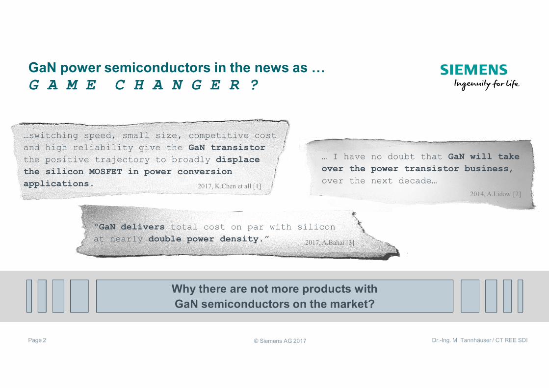
GaN power semiconductors in the news as …G A M E C H A N G E R ?
Why there are not more products withGaN semiconductors on the market?
… I have no doubt that GaN will takeover the power transistor business,over the next decade…
2014, A.Lidow [2]
…switching speed, small size, competitive costand high reliability give the GaN transistorthe positive trajectory to broadly displacethe silicon MOSFET in power conversionapplications. 2017, K.Chen et all [1]
“GaN delivers total cost on par with siliconat nearly double power density.” 2017, A.Bahai [3]

© Siemens AG 2017Page 3 Dr.-Ing. M. Tannhäuser / CT REE SDI
What are major challenges usingGaN power semiconductors?
… from Power Electronics System view
© Siemens AG 2017Page 4 Dr.-Ing. M. Tannhäuser / CT REE SDI
1
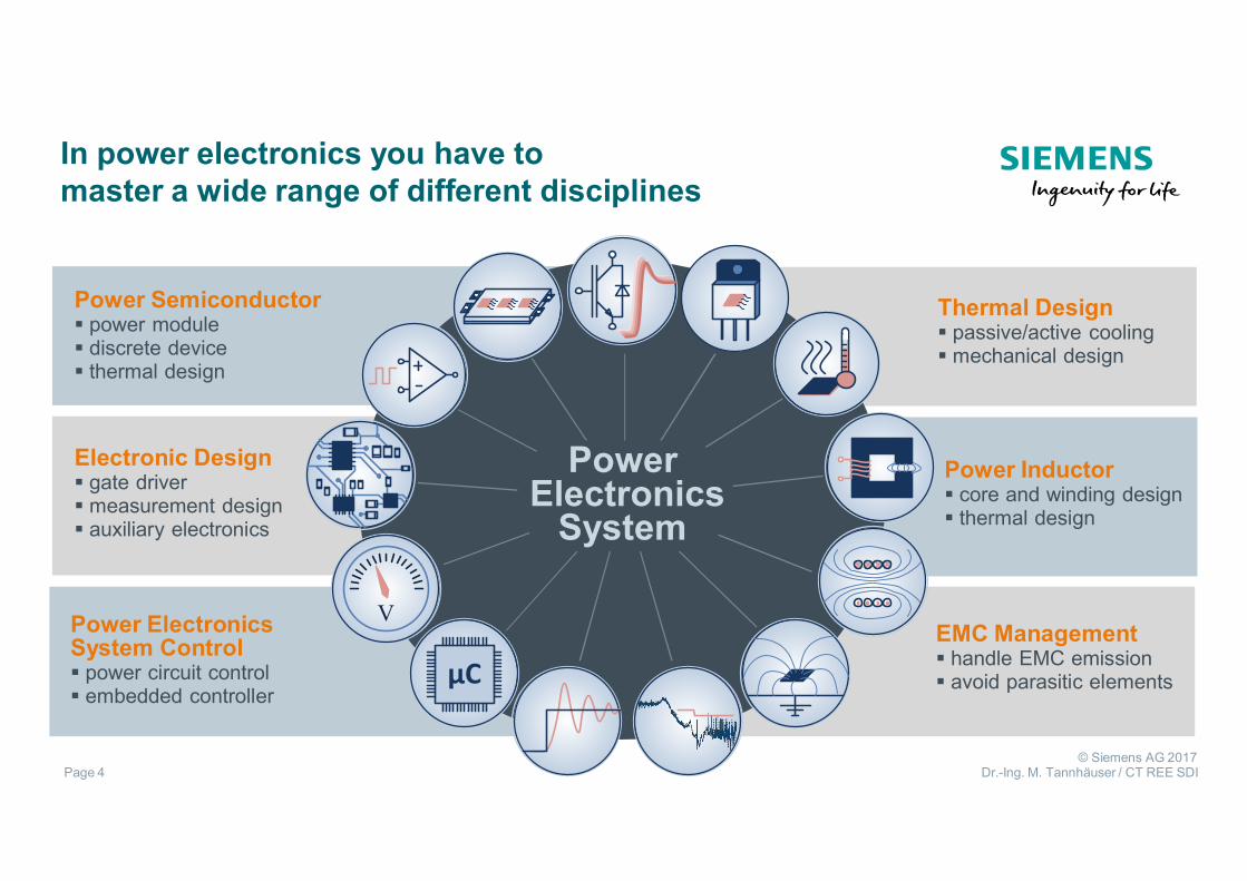
In power electronics you have tomaster a wide range of different disciplines
XY
µC
Power Semiconductorƒ power moduleƒ discrete deviceƒ thermal design
V
Electronic Designƒ gate driverƒ measurement designƒ auxiliary electronics
Power ElectronicsSystem Controlƒ power circuit controlƒ embedded controller
Power Inductorƒ core and winding designƒ thermal design
EMC Managementƒ handle EMC emissionƒ avoid parasitic elements
Thermal Designƒ passive/active coolingƒ mechanical design
PowerElectronics
System
© Siemens AG 2017
© Siemens AG 2017Page 5 Dr.-Ing. M. Tannhäuser / CT REE SDI
1
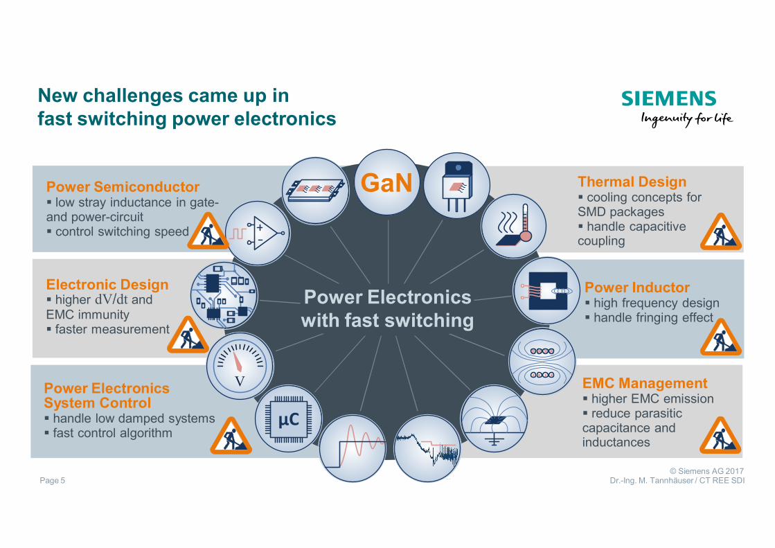
New challenges came up infast switching power electronics
XY
µC
Power Semiconductorƒ low stray inductance in gate-and power-circuitƒ control switching speed
V
Electronic Designƒ higher dV/dt andEMC immunityƒ faster measurement
Power ElectronicsSystem Controlƒ handle low damped systemsƒ fast control algorithm
Power Inductorƒ high frequency designƒ handle fringing effect
EMC Managementƒ higher EMC emissionƒ reduce parasiticcapacitance andinductances
Thermal Designƒ cooling concepts forSMD packagesƒ handle capacitivecoupling
Power Electronicswith fast switching
GaN
© Siemens AG 2017

© Siemens AG 2017Page 6 Dr.-Ing. M. Tannhäuser / CT REE SDI
SMD package and thermal management
discreteTO packages
discreteSMD package
Why do we need power semiconductors in SMDpackages?
ƒ lower stray inductance in the power circuitƒ better control of the gate voltageƒ easy and full automated manufacturing
RPCB,v1: Local thermal resistance from device pad vertical trough PCB to TIMRPCB,v2: Distributed vertical thermal resistance trough PCBRPCB,sp: Spreading resistance within the copper layers of the PCBRPCB-A: Convection resistance from the PCB surface to ambient
Thermal equivalent circuit of the PCB
How can we influence/optimize the thermalmanagement of SMD power semiconductoron a standard PCB?
© Siemens AG 2017Page 7 Dr.-Ing. M. Tannhäuser / CT REE SDI
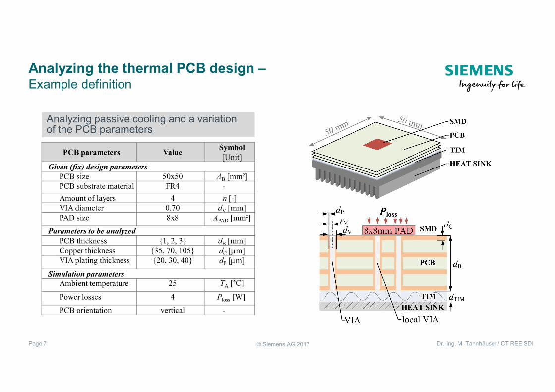
Analyzing the thermal PCB design –Example definition
Analyzing passive cooling and a variationof the PCB parameters
PCB parameters Value Symbol[Unit]
Given (fix) design parametersPCB size 50x50 AB [mm²]PCB substrate material FR4 -Amount of layers 4 n [-]VIA diameter 0.70 dV [mm]PAD size 8x8 APAD [mm²]
Parameters to be analyzedPCB thickness {1, 2, 3} dB [mm]Copper thickness {35, 70, 105} dC [λm]VIA plating thickness {20, 30, 40} dP [λm]
Simulation parametersAmbient temperature 25 TA [°C]
Power losses 4 Ploss [W]
PCB orientation vertical -

© Siemens AG 2017Page 8 Dr.-Ing. M. Tannhäuser / CT REE SDI
Analyzing the thermal PCB design –Thermal spreading within the PCB
Setup Iƒ with local thermal VIAsƒ without thermal spreading
Rth,PAD-HS
Designguide
5.8 K/W100 %
3.4 K/W59 %
3.5 K/W60 %
35 µm
Amount of local thermalVIAs should be chosen byconsidering the wholethermal resistance
With the combination of local VIAsand thermal spreading a goodperformance can be reached witha standard PCB
Setup IIƒ without local thermal VIAsƒ with thermal spreading
4.8 K/W83 %
8.2 K/W141 %
Temperature [°C]
Copper layers(4 layers)
70 µm 105 µm35 µm 70 µm
Setup IIIƒ with local thermal VIAsƒ with thermal spreading
Thermal spreading is important toreach good thermal properties. Thecopper thickness has a majorinfluence
from device padto heat sink

© Siemens AG 2017Page 9 Dr.-Ing. M. Tannhäuser / CT REE SDI
Analyzing the thermal PCB design –Variation of cooling method
Setup Iƒ without fanƒ without heat sink
Setup IIƒ without fanƒ with heat sink
Setup IIIƒ with fanƒ without heat sink
Setup IVƒ with fanƒ with heat sink
Power lossesat ΧT = 60 K
Rth,PAD-A
Properties/Application
17.5 K/W100 %
8.93 K/W51 %
12.4 K/W71 %
4.63 K/W26 %
3.43 W 4.84 W 6.72 W 13.0 W
ƒ passive coolingƒ small size and low weightƒ easy manufacturingƒ cheap
ƒ passive coolingƒ sealed housing/enclosure
ƒ small size and low weightƒ easy manufacturingƒ cheap
ƒmaximum power lossesƒ higher cost
Temperature [°C]
from device padto ambient

© Siemens AG 2017Page 10 Dr.-Ing. M. Tannhäuser / CT REE SDI
Analyzing the thermal PCB design –How to influence the thermal performance?
Thermal spreading within the PCB is as important as the use of local thermal VIAsƒ the thickness has a major influence to the PCB spreading resistanceƒ a good thermal spreading decreases the negative influence of a TIM and the board thicknessƒ less local VIAs allow a degree of freedom for the electrical design of the power cellƒ a thermal PCB resistance of 3 to 4 K/W can be reached with a standard PCB with passive cooling
The relevance of the thermal PCB design depends on the cooling method and applicationApplication with low power lossesƒ passive cooling without heat sink and fan is possibleƒ easy and high volume manufacturing can be achievedƒ low cost for manufacturing and maintenanceApplication with high power lossesƒ a fan and heat sink is needed
An optimal thermal PCB design needs in any case further investigations and calculationsThe paper shows examples to understand the possibilities and limits of the thermal PCB design

© Siemens AG 2017Page 11 Dr.-Ing. M. Tannhäuser / CT REE SDI
GaN converter prototype with a thermal managementonly by the PCB design
Converter prototype with GaN SMD power semiconductors demonstrates a passive coolingwithout heat sink and fan

© Siemens AG 2017Page 12 Dr.-Ing. M. Tannhäuser / CT REE SDI
GaN converter prototypeMeasurement results (single phase)
Measurement conditionsPower: 1 kW (single phase)Switching frequency: 175 kHzCooling: Passive (no fan, no heat sink, TA = 25°C)
SMD in detail SMD temperature = 57°C
Sinusoidal output voltage Efficiency measurement

© Siemens AG 2017Page 13 Dr.-Ing. M. Tannhäuser / CT REE SDI
Conclusion and outlookFuture trend: Integrated Power Electronics
FUTURE“all-digital”
Integrated Power Electronics
GaN enables newPower Electronics Systemsƒ higher switching speedƒ higher efficienciesƒ smaller passive componentsƒ smaller and lighter converter systemsƒ easy and high volume manufacturingƒ lower system costƒ easy power scalingƒ higher system performanceƒ etc…
Challenges for future fast switching Integrated Power Electronicsƒ cooling concepts for SMD power semiconductorsƒ power inductors for high switching frequencyƒ auxiliary electronics (gate-driver, isolators, measurements) with high EMC-immunityƒ fast control concepts for PE systems with low dampingƒ concepts to handle high EMC emissionƒ new topologies for high switching speed and frequency
[4]
© Siemens AG 2017Page 14 Dr.-Ing. M. Tannhäuser / CT REE SDI
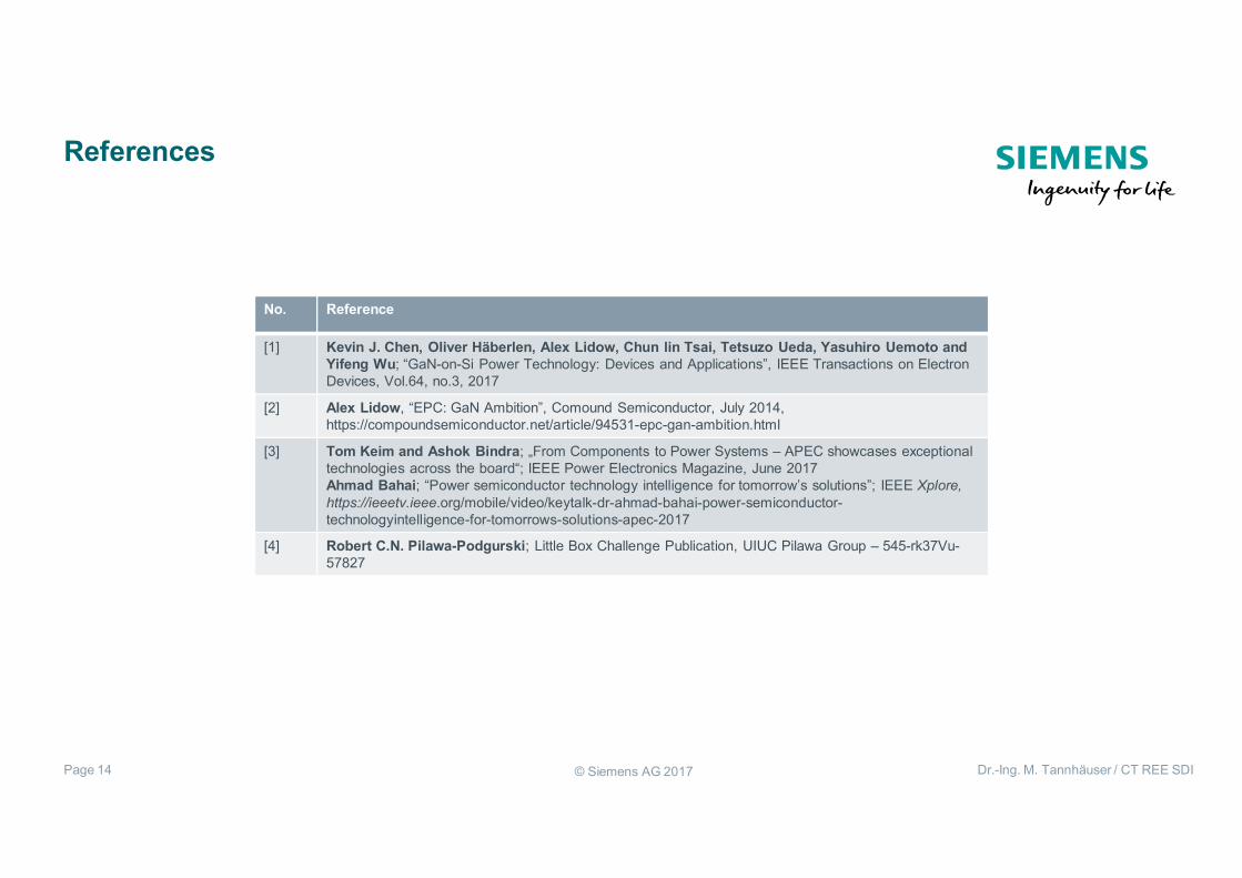
References
No. Reference
[1] Kevin J. Chen, Oliver Häberlen, Alex Lidow, Chun lin Tsai, Tetsuzo Ueda, Yasuhiro Uemoto andYifeng Wu; “GaN-on-Si Power Technology: Devices and Applications”, IEEE Transactions on ElectronDevices, Vol.64, no.3, 2017
[2] Alex Lidow, “EPC: GaN Ambition”, Comound Semiconductor, July 2014,https://compoundsemiconductor.net/article/94531-epc-gan-ambition.html
[3] Tom Keim and Ashok Bindra; „From Components to Power Systems – APEC showcases exceptionaltechnologies across the board“; IEEE Power Electronics Magazine, June 2017Ahmad Bahai; “Power semiconductor technology intelligence for tomorrow’s solutions”; IEEE Xplore,https://ieeetv.ieee.org/mobile/video/keytalk-dr-ahmad-bahai-power-semiconductor-technologyintelligence-for-tomorrows-solutions-apec-2017
[4] Robert C.N. Pilawa-Podgurski; Little Box Challenge Publication, UIUC Pilawa Group – 545-rk37Vu-57827

© Siemens AG 2017Page 15 Dr.-Ing. M. Tannhäuser / CT REE SDI
Contact
Siemens AGCorporate TechnologySoftware Defined Inverter – Digital Power Electronics
CT REE SDIDr.-Ing. Marvin TannhäuserSenior Key Expert
E-mail: [email protected]
Frauenauracher Straße 8091056 ErlangenGERMANY