plasmonic resonance enhanced polarization-sensitive ...yep/papers/acs nano... · enhancement by...
TRANSCRIPT
Plasmonic Resonance Enhanced Polarization-Sensitive Photodetection by Black Phosphorusin Near InfraredPrabhu K. Venuthurumilli,† Peide D. Ye,‡ and Xianfan Xu*,†,‡
†School of Mechanical Engineering and Birck Nanotechnology Center, Purdue University, West Lafayette, Indiana 47907, UnitedStates‡School of Electrical and Computer Engineering, Purdue University, West Lafayette, Indiana 47907, United States
*S Supporting Information
ABSTRACT: Black phosphorus, a recently intensely investigated two-dimensional material, is promising for electronic and optoelectronicapplications due to its higher mobility and thickness-dependent directband gap. With its low direct band gap and anisotropic properties innature, black phosphorus is also suitable for near-infrared polarization-sensitive photodetection. To enhance photoresponsivity of a blackphosphorus based photodetector, we demonstrate two designs ofplasmonic structures. In the first design, plasmonic bowtie antennas areused to increase the photocurrent, particularly in the armchairdirection, where the optical absorption is higher than that in thezigzag direction. The simulated electric field distribution with bowtiestructures shows enhanced optical absorption by localized surface plasmons. In the second design, bowtie apertures areused to enhance the inherent polarization selectivity of black phosphorus. A high photocurrent ratio (armchair to zigzag)of 8.7 is obtained. We choose a near-infrared wavelength of 1550 nm to demonstrate the photosensitivity enhancement andpolarization selectivity, as it is useful for applications including telecommunication, remote sensing, biological imaging, andinfrared polarimetry imaging.
KEYWORDS: black phosphorus, plasmonics, polarization-sensitive, near-infrared, photodetector, bowtie antenna, bowtie aperture
Two-dimensional materials are of immense interest dueto their extraordinary properties compared to theirbulk counterparts. In addition to graphene1,2 and
transition metal dichalcogenides3,4 such as MoS2,5,6 few-layer
black phosphorus (BP) is intensively studied recently due to itsunique properties including high mobility7 and a thickness-dependent direct band gap, ∼0.3 eV in bulk and around 1.5 eVin monolayer,8−12 whereas MoS2 has a direct band gap only as amonolayer.13,14 Well-behaved field effect transistors in BP havebeen demonstrated.15,16 With these extraordinary properties,BP is a promising candidate for electronic and optoelectronicapplications including scaled high-performance transistors,17
solar cells,18 and photodetectors.19,20
The unique thickness-dependent direct band gap makes BPespecially promising for photodetection. In this work weinvestigate methods to enhance photoresponse in blackphosphorus photodetectors at near-IR wavelength, which canfind use in various applications including telecommunication,remote sensing, and biological imaging.21 Conventional IRdetectors require either an expensive fabrication process such asmolecular beam epitaxy, low-temperature operation, or both.Moreover, integration of these conventional narrow band gap
semiconductors with traditional electronic materials such assilicon is difficult due to lattice mismatch.22 In contrast, thelayered structure of black phosphorus is suitable for monolithicintegration with silicon and even with flexible substrates.23 BPphotodetectors have been reported.16,19,20,24−26 However, theperformance of most of these photodetectors is limited becauseof low light absorption in thin films. On the other hand,plasmonic structure enhanced photoresponsivity at visiblewavelengths has been demonstrated in graphene27,28 andMoS2.
29 Here, we demonstrate enhanced photosensitivity andpolarization selectivity in BP using plasmonic structures at thenear-IR wavelength of 1550 nm. The same methods can beused for longer wavelengths up to the band gap of BP, ∼4μm.11 We report two designs of plasmonic structures toenhance photosensitivity and polarization-sensitive photo-detection. In the first design, we use bowtie antennas toenhance absorption and hence the photocurrent. Computa-tional design shows that the enhanced absorption is due to field
Received: March 4, 2018Accepted: April 23, 2018Published: April 23, 2018
Artic
lewww.acsnano.orgCite This: ACS Nano 2018, 12, 4861−4867
© 2018 American Chemical Society 4861 DOI: 10.1021/acsnano.8b01660ACS Nano 2018, 12, 4861−4867
Dow
nloa
ded
via
PUR
DU
E U
NIV
on
July
6, 2
018
at 1
6:08
:39
(UT
C).
Se
e ht
tps:
//pub
s.ac
s.or
g/sh
arin
ggui
delin
es f
or o
ptio
ns o
n ho
w to
legi
timat
ely
shar
e pu
blis
hed
artic
les.
enhancement by bowtie plasmonic structures. In the seconddesign, we use bowtie apertures (or bowtie aperture antennas)to enhance the inherent polarization selectivity of BP. BP has apuckered layer structure, resulting in anisotropic in-planeproperties30−32 along its two principal armchair and zigzagdirections including anisotropic optical properties, where thearmchair direction has greater absorption compared to thatalong the zigzag direction.26,33,34 Inversion symmetry andmirror reflection symmetry of a crystal structure in the zigzagdirection forbid transitions of photons polarized in the zigzagdirection with band gap energy and significantly reduceabsorption of photons with higher energies.26 The transmissionof light through bowtie apertures is also polarization depend-ent35 and hence can further enhance the polarization selectivityof BP. Here we experimentally demonstrate a bowtie apertureenhanced BP detector with a photocurrent ratio (armchair tozigzag) of 8.7, which is useful in IR polarimetry imaging.36
RESULTS AND DISCUSSIONBP flakes are prepared by tape exfoliation from bulk onto aSiO2/Si substrate (see Methods). In the first design, we usebowtie antenna plasmonic structures to enhance the photo-response. Figure 1a shows an optical image of two devices on
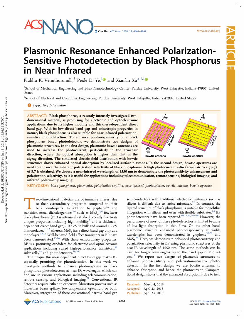
the same flake: (i) without plasmonic structures and (ii) withbowtie antenna plasmonic structures. The plasmonic structuresand contacts are fabricated using standard e-beam lithography,metallization, and lift-off processes. Thin-film metal of Ti/Au(5 nm/75 nm) is deposited for both the plasmonic structuresand contacts. A scanning electron microscopy (SEM) image ofthe bowtie structures of device (ii) in Figure 1a is shown inFigure 1b. The flake is 135 nm thick, as characterized by atomicforce microscopy (AFM), and is shown in Figure 1c. PolarizedRaman spectroscopy is used to determine the lattice orientationof BP.31 Figure 1d shows the Raman spectrum when the
polarization is along the x-direction (Figure 1a), indicating thatthe x-direction is the armchair direction.31 The device channellengths (as seen in Figure 1a) are designed along the armchairdirection for better photocarrier collection. This is because ofshorter carrier transit time due to higher mobility along thearmchair direction than that along the zigzag direction.20 Theabsorption of BP is also stronger along the armchair directionas compared to the zigzag direction.26,31 Hence, the bowtiestructures are aligned by fabricating along the armchairdirection as shown in Figure 1b to enhance armchair absorptionby the localized surface plasmons.To study the photoresponse of the devices, scanning
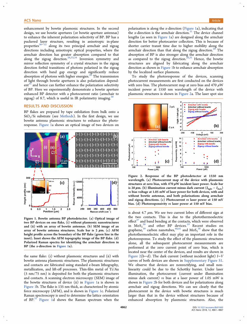
photocurrent measurements are first conducted on the deviceswith zero bias. The photocurrent map at zero bias and 470 μWincident power at 1550 nm wavelength of the device withplasmonic structures is shown in Figure 2a. The laser spot size
is about 4.7 μm. We see two current lobes of different sign atthe two contacts. This is due to the photothermoelectriceffect37 and band bending at the contacts, which were observedin MoS2
38 and other BP devices.19 Recent studies ongraphene,39 carbon nanotubes,40,41 and MoS2
38 show that thephotothermoelectric effect may play an important role in thephotoresponse. To study the effect of the plasmonic structuresalone, all the subsequent photocurrent measurements areperformed at the zero current point of zero bias, which islocated near the center of the devices, and results are shown inFigure 2(b−d). The dark current (without incident light) I−Vcurves of both devices are shown in Supplementary Figure S1.We observe that devices are nonrectifying, and small non-linearity could be due to the Schottky barrier. Under laserillumination, the photocurrent (current under illuminationminus dark current) vs bias at a laser power of 1.05 mW isshown in Figure 2b for both devices and for polarizations alongarmchair and zigzag directions. We can see clearly that thephotocurrent in the device with bowtie structures is muchlarger than that in the device without structures because ofenhanced absorption by plasmonic structures. Also, the
Figure 1. Bowtie antenna BP photodetector. (a) Optical image oftwo BP devices on one flake, (i) without plasmonic nanostructuresand (ii) with an array of bowtie antennas. (b) SEM image of anarray of bowtie antenna structures. Scale bar is 2 μm. (c) AFMheight profile across the boundary of the BP flake (green line in theinset). Inset shows the AFM topography image of the BP flake. (d)Polarized Raman spectra for identifying the armchair direction inBP (the x-direction in Figure 1a).
Figure 2. Response of the BP photodetector at 1550 nmwavelength. (a) Photocurrent map of the device with plasmonicstructures at zero bias, with 470 μW incident laser power. Scale baris 20 μm. (b) Illumination current minus dark current (Ilight − Idark)vs bias voltage at 1.05 mW of laser power for both devices, with andwithout bowtie antennas, and both polarizations along armchairand zigzag directions. (c) Photocurrent vs laser power at 150 mVbias. (d) Photoresponsivity vs laser power at 150 mV bias.
ACS Nano Article
DOI: 10.1021/acsnano.8b01660ACS Nano 2018, 12, 4861−4867
4862
photocurrent when illuminated along the armchair direction islarger than that along the zigzag direction due to higherabsorption in BP and higher transmission through bowtieantennas. The photocurrent increases with bias because ofextraction of more electron−hole pairs before they arerecombined. The photocurrent vs laser power at 150 mV biasis shown in Figure 2c for both devices and illuminationpolarizations. The photocurrent increases with laser powerbecause of generation of more electron hole pairs. Thephotoresponsivity, defined as photocurrent divided by laserpower, at 150 mV bias is shown in Figure 2d. Thephotoresponsivity decreases with increasing laser power,which is a common behavior of photodetectors due tosaturation of the electron−hole pair generation at high laserpower and the increased surface recombination.42
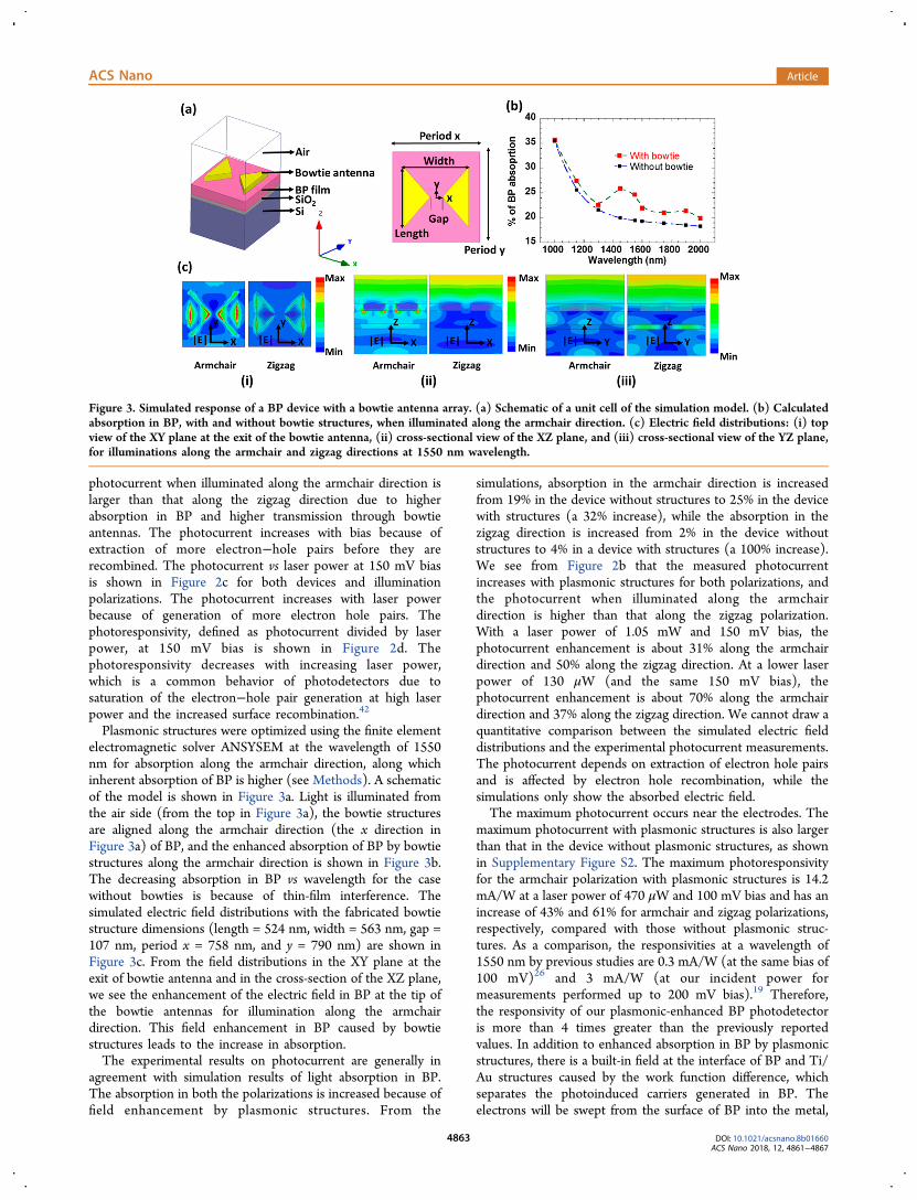
Plasmonic structures were optimized using the finite elementelectromagnetic solver ANSYSEM at the wavelength of 1550nm for absorption along the armchair direction, along whichinherent absorption of BP is higher (see Methods). A schematicof the model is shown in Figure 3a. Light is illuminated fromthe air side (from the top in Figure 3a), the bowtie structuresare aligned along the armchair direction (the x direction inFigure 3a) of BP, and the enhanced absorption of BP by bowtiestructures along the armchair direction is shown in Figure 3b.The decreasing absorption in BP vs wavelength for the casewithout bowties is because of thin-film interference. Thesimulated electric field distributions with the fabricated bowtiestructure dimensions (length = 524 nm, width = 563 nm, gap =107 nm, period x = 758 nm, and y = 790 nm) are shown inFigure 3c. From the field distributions in the XY plane at theexit of bowtie antenna and in the cross-section of the XZ plane,we see the enhancement of the electric field in BP at the tip ofthe bowtie antennas for illumination along the armchairdirection. This field enhancement in BP caused by bowtiestructures leads to the increase in absorption.The experimental results on photocurrent are generally in
agreement with simulation results of light absorption in BP.The absorption in both the polarizations is increased because offield enhancement by plasmonic structures. From the
simulations, absorption in the armchair direction is increasedfrom 19% in the device without structures to 25% in the devicewith structures (a 32% increase), while the absorption in thezigzag direction is increased from 2% in the device withoutstructures to 4% in a device with structures (a 100% increase).We see from Figure 2b that the measured photocurrentincreases with plasmonic structures for both polarizations, andthe photocurrent when illuminated along the armchairdirection is higher than that along the zigzag polarization.With a laser power of 1.05 mW and 150 mV bias, thephotocurrent enhancement is about 31% along the armchairdirection and 50% along the zigzag direction. At a lower laserpower of 130 μW (and the same 150 mV bias), thephotocurrent enhancement is about 70% along the armchairdirection and 37% along the zigzag direction. We cannot draw aquantitative comparison between the simulated electric fielddistributions and the experimental photocurrent measurements.The photocurrent depends on extraction of electron hole pairsand is affected by electron hole recombination, while thesimulations only show the absorbed electric field.The maximum photocurrent occurs near the electrodes. The
maximum photocurrent with plasmonic structures is also largerthan that in the device without plasmonic structures, as shownin Supplementary Figure S2. The maximum photoresponsivityfor the armchair polarization with plasmonic structures is 14.2mA/W at a laser power of 470 μW and 100 mV bias and has anincrease of 43% and 61% for armchair and zigzag polarizations,respectively, compared with those without plasmonic struc-tures. As a comparison, the responsivities at a wavelength of1550 nm by previous studies are 0.3 mA/W (at the same bias of100 mV)26 and 3 mA/W (at our incident power formeasurements performed up to 200 mV bias).19 Therefore,the responsivity of our plasmonic-enhanced BP photodetectoris more than 4 times greater than the previously reportedvalues. In addition to enhanced absorption in BP by plasmonicstructures, there is a built-in field at the interface of BP and Ti/Au structures caused by the work function difference, whichseparates the photoinduced carriers generated in BP. Theelectrons will be swept from the surface of BP into the metal,
Figure 3. Simulated response of a BP device with a bowtie antenna array. (a) Schematic of a unit cell of the simulation model. (b) Calculatedabsorption in BP, with and without bowtie structures, when illuminated along the armchair direction. (c) Electric field distributions: (i) topview of the XY plane at the exit of the bowtie antenna, (ii) cross-sectional view of the XZ plane, and (iii) cross-sectional view of the YZ plane,for illuminations along the armchair and zigzag directions at 1550 nm wavelength.
ACS Nano Article
DOI: 10.1021/acsnano.8b01660ACS Nano 2018, 12, 4861−4867
4863
while there is a small barrier for holes as seen from the banddiagram.16 This can lead to longer recombination time and cancause more photocurrent, as was observed in graphene.43,44
Also, very limited photocurrent was reported by hot electronsfrom gold plasmonic structures injected into silicon over theSchottky barrier.45 In our experiments, we are unable todistinguish the contribution between the hot electrons frommetal and photoinduced carriers in BP, as our incident energyis greater than the band gap of BP. However, we expect the hotelectron contribution to be weak, as there is no barrier forelectrons to return to the gold by the built-in field at theinterface.We performed the transient current measurements by
mechanically modulating the incident light. However, we arelimited by the frequency of the mechanical chopper to obtainthe actual response time of devices as shown in theSupplementary Figure S3. From our measurements, theresponse time of the devices, with and without bowtiestructures, is less than 90 μs, for light polarization alongarmchair and zigzag directions. The reported intrinsic responsetime of the black phosphorus photodetector can be as fast as∼75 ps along both armchair and zigzag directions.46 Since weexpect the hot electron contribution to be weak, the responsetime of devices with and without plasmonic structures would besimilar to those observed in graphene.43
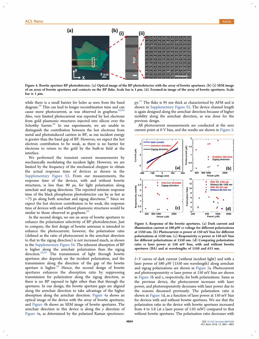
In the second design, we use an array of bowtie apertures toenhance the polarization selectivity of BP photodetection. Justto compare, the first design of bowtie antennas is intended toenhance the photocurrent; however, the polarization ratio(defined as the ratio of photocurrent in the armchair directionto that in the zigzag direction) is not increased much, as shownin the Supplementary Figure S4. The inherent absorption of BPis higher along the armchair polarization than the zigzagdirection.26,31 The transmission of light through bowtieapertures also depends on the incident polarization, and thetransmission along the direction of the gap of the bowtieaperture is higher.35 Hence, the second design of bowtieapertures enhances the absorption ratio by suppressingtransmission for polarization along the zigzag direction, asthere is no BP exposed to light other than that through theapertures. In our design, the bowtie aperture gaps are alignedalong the armchair direction to take advantage of the higherabsorption along the armchair direction. Figure 4a shows anoptical image of the device with the array of bowtie apertures,and Figure 4b shows an SEM image of bowtie apertures. Thearmchair direction in this device is along the y direction ofFigure 4a, as determined by the polarized Raman spectrosco-
py.31 The flake is 95 nm thick as characterized by AFM and isshown in Supplementary Figure S5. The device channel lengthis again designed along the armchair direction because of highermobility along the armchair direction, as was done for theprevious design.All photocurrent measurements are conducted at the zero
current point at 0 V bias, and the results are shown in Figure 5.
I−V curves of dark current (without incident light) and with alaser power of 580 μW (1550 nm wavelength) along armchairand zigzag polarizations are shown in Figure 5a. Photocurrentand photoresponsivity vs laser power at 150 mV bias are shownin Figure 5b and c, respectively, for both polarizations. Same asthe previous device, the photocurrent increases with laserpower, and photoresponsivity decreases with laser power due tothe reasons discussed previously. The polarization ratio isshown in Figure 5d, as a function of laser power at 150 mV biasfor devices with and without bowtie apertures. We see that thepolarization ratio in the device with bowtie apertures increasedfrom 4 to 5.8 (at a laser power of 1.05 mW) compared to thatwithout bowtie apertures. The polarization ratio decreases with
Figure 4. Bowtie aperture BP photodetector. (a) Optical image of the BP photodetector with the array of bowtie apertures. (b) (i) SEM imageof an array of bowtie apertures and contacts on the BP flake. Scale bar is 1 μm. (ii) Zoomed-in image of the array of bowtie apertures. Scalebar is 1 μm.
Figure 5. Response of the bowtie apertures. (a) Dark current andillumination current at 580 μW vs voltage for different polarizationsat 1550 nm. (b) Photocurrent vs power at 150 mV bias for differentpolarizations at 1550 nm. (c) Responsivity vs power at 150 mV biasfor different polarizations at 1550 nm. (d) Comparing polarizationratio vs laser power at 150 mV bias, with and without bowtieapertures (BA) and at wavelengths of 1550 and 633 nm.
ACS Nano Article
DOI: 10.1021/acsnano.8b01660ACS Nano 2018, 12, 4861−4867
4864
laser power both with and without bowtie apertures. Thepossible reason for the decrease in polarization ratio withincrease in laser power is the saturation of increasedphotocurrent extraction in the armchair direction as thephotoabsorption increases. At a lower laser power of 470μW, a higher polarization ratio of 8.7 is obtained in the bowtieaperture BP photodetector. I−V curves obtained at the laserpower of 470 μW for both polarization directions are shown inSupplementary Figure S6. Also shown in Figure 5d is themeasurement using a 633 nm wavelength. It is seen that thepolarization ratio at 633 nm does not change much, as theresponse of the bowtie aperture strongly depends on thewavelength due to its plasmonic resonance. It was reported thatpatterned Au nanostructures can locally influence the grapheneFermi energy.47,48 We do not expect Au patterns to stronglyinfluence the transport properties in our devices of bulk BP. Inour first device, although 20% of BP is covered by metal, thedark currents of both devices (with and without bowties) aresimilar, as shown in Supplementary Figure 1. For the seconddesign, resistivity of the device with bowtie apertures isestimated to be 4.71 Ω cm, while the resistivity of the devicewithout plasmonic structures shown in Figure 1 is 5.28 Ω cm.The 10% variation in resistivity could be because of device-to-device variation as well as a minor surface effect by gold.BP photodetectors with bowtie apertures shown in Figure 4
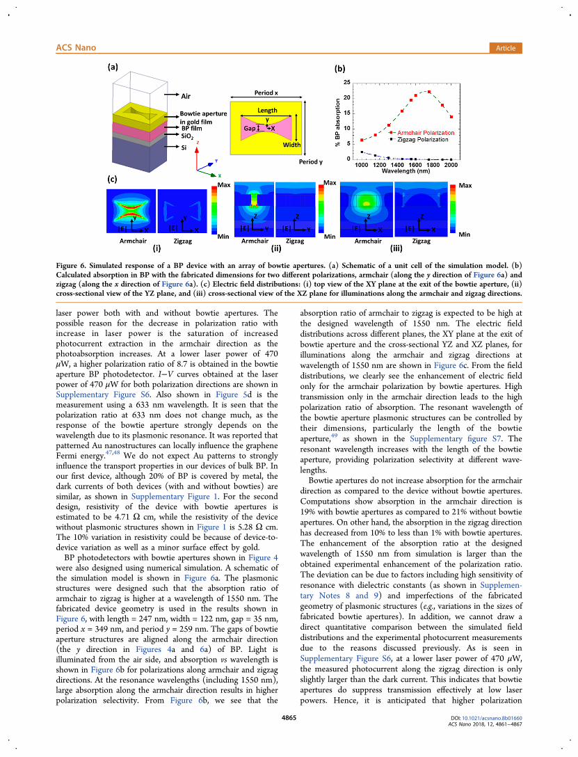
were also designed using numerical simulation. A schematic ofthe simulation model is shown in Figure 6a. The plasmonicstructures were designed such that the absorption ratio ofarmchair to zigzag is higher at a wavelength of 1550 nm. Thefabricated device geometry is used in the results shown inFigure 6, with length = 247 nm, width = 122 nm, gap = 35 nm,period x = 349 nm, and period y = 259 nm. The gaps of bowtieaperture structures are aligned along the armchair direction(the y direction in Figures 4a and 6a) of BP. Light isilluminated from the air side, and absorption vs wavelength isshown in Figure 6b for polarizations along armchair and zigzagdirections. At the resonance wavelengths (including 1550 nm),large absorption along the armchair direction results in higherpolarization selectivity. From Figure 6b, we see that the
absorption ratio of armchair to zigzag is expected to be high atthe designed wavelength of 1550 nm. The electric fielddistributions across different planes, the XY plane at the exit ofbowtie aperture and the cross-sectional YZ and XZ planes, forilluminations along the armchair and zigzag directions atwavelength of 1550 nm are shown in Figure 6c. From the fielddistributions, we clearly see the enhancement of electric fieldonly for the armchair polarization by bowtie apertures. Hightransmission only in the armchair direction leads to the highpolarization ratio of absorption. The resonant wavelength ofthe bowtie aperture plasmonic structures can be controlled bytheir dimensions, particularly the length of the bowtieaperture,49 as shown in the Supplementary figure S7. Theresonant wavelength increases with the length of the bowtieaperture, providing polarization selectivity at different wave-lengths.Bowtie apertures do not increase absorption for the armchair
direction as compared to the device without bowtie apertures.Computations show absorption in the armchair direction is19% with bowtie apertures as compared to 21% without bowtieapertures. On other hand, the absorption in the zigzag directionhas decreased from 10% to less than 1% with bowtie apertures.The enhancement of the absorption ratio at the designedwavelength of 1550 nm from simulation is larger than theobtained experimental enhancement of the polarization ratio.The deviation can be due to factors including high sensitivity ofresonance with dielectric constants (as shown in Supplemen-tary Notes 8 and 9) and imperfections of the fabricatedgeometry of plasmonic structures (e.g., variations in the sizes offabricated bowtie apertures). In addition, we cannot draw adirect quantitative comparison between the simulated fielddistributions and the experimental photocurrent measurementsdue to the reasons discussed previously. As is seen inSupplementary Figure S6, at a lower laser power of 470 μW,the measured photocurrent along the zigzag direction is onlyslightly larger than the dark current. This indicates that bowtieapertures do suppress transmission effectively at low laserpowers. Hence, it is anticipated that higher polarization
Figure 6. Simulated response of a BP device with an array of bowtie apertures. (a) Schematic of a unit cell of the simulation model. (b)Calculated absorption in BP with the fabricated dimensions for two different polarizations, armchair (along the y direction of Figure 6a) andzigzag (along the x direction of Figure 6a). (c) Electric field distributions: (i) top view of the XY plane at the exit of the bowtie aperture, (ii)cross-sectional view of the YZ plane, and (iii) cross-sectional view of the XZ plane for illuminations along the armchair and zigzag directions.
ACS Nano Article
DOI: 10.1021/acsnano.8b01660ACS Nano 2018, 12, 4861−4867
4865
selectivity can be realized when the incident power is lower,such as in imaging.
CONCLUSIONSIn conclusion, we demonstrated enhanced photosensitivity andpolarization selectivity of black phosphorus photodetectorsusing resonant plasmonic structures. In the first design usingbowtie antennas, we obtained an enhancement of 70% in thephotoresponse in comparison to a device without plasmonicstructures. The responsivity of the bowtie antenna BPphotodetector, even at lower bias, is more than 4 times greaterthan previously reported values. Simulation shows thatabsorption is increased due to the field enhancement by theplasmonic structures. In the second design using bowtieapertures, photocurrent can be effectively suppressed for zigzagpolarization, particularly when the incident power is low such asin imaging. An armchair to zigzag photocurrent ratio of 8.7 hasbeen demonstrated. Enhanced photosensitivity and polarizationselectivity at near-infrared wavelengths will be useful in variousapplications including telecommunication, remote sensing,biological imaging, and infrared polarimetry imaging.
METHODSSample Preparation. BP flakes are exfoliated from bulk using
Scotch tape on a SiO2/Si substrate. The thickness of the oxide layer is50 nm. BP flakes that are large and uniform are chosen frominspection under an optical microscope. The thickness of the flakes ischaracterized using AFM, and the crystal direction of BP is determinedby polarized Raman spectroscopy using a HORIBA LabRAM HR800Raman spectrometer.Optical Property Measurements. Optical properties of the BP
flakes at 1550 nm are determined by exfoliating flakes onto the glasssubstrate and by measuring the reflectance (R) and transmittance (T)of the flakes (shown in Supplementary Figure S9). The reflectance ofeach sample is measured using a reference of silver-coated mirror withknown reflectivity. The optical constants are then obtained fromFresnel equations using the measured reflectance, transmittance, andthickness of the films for both armchair and zigzag directions.Numerical Computation. Plasmonic structures are modeled
using the finite element electromagnetic solver ANSYS EM 17.1with periodic boundary conditions. The frequency-dependent opticalconstants for gold are taken from Johnson and Christy.50 For BP,experimentally obtained in-plane optical constants at 1550 nm ofsimilar thickness were used for the armchair and zigzag directions forall wavelengths. Out-of-plane dielectric constants are considered theaverage of armchair and zigzag directions.Fabrication. The optimized plasmonic structures and metal
contacts are fabricated onto the flakes on a SiO2/Si substrate usingstandard electron beam lithography, metallization, and lift-offprocesses. Ti/Au (5/75 nm) metal films are prepared using e-beamevaporation.Photocurrent Measurements. The photoresponse of the devices
is measured using a Keithley 2612 system. Scanning photocurrentmeasurements are performed using a piezostage. All optical andelectrical measurements are performed in ambient atmosphere. Thesamples are stored in a vacuum in between measurements to avoid BPdegradation.
ASSOCIATED CONTENT*S Supporting InformationThe Supporting Information is available free of charge on theACS Publications website at DOI: 10.1021/acsnano.8b01660.
Dark current of devices with and without bowtieantennas, photocurrent maps of devices with and withoutbowtie antenna, response time of the BP photodetector,the polarization ratio with and without bowtie structures,
thickness of the BP in bowtie aperture BP photodetector,I−V curve of bowtie aperture BP photodetector at 470μW, resonant wavelength of bowtie aperture array,sensitivity of resonant wavelength to optical constants,and measurement of optical property of BP (PDF)
AUTHOR INFORMATION
Corresponding Author*E-mail: [email protected].
ORCIDPeide D. Ye: 0000-0001-8466-9745Xianfan Xu: 0000-0003-0580-4625Author ContributionsX.X. conceived the idea and supervised the numerical analysesand experiments. P.V. led the design, fabrication, andmeasurements of BP photodetectors. All authors analyzed theresults and cowrote the manuscript.
NotesThe authors declare no competing financial interest.
ACKNOWLEDGMENTS
This work was supported by AFOSR/NSF under the EFRI2-DARE Grant EFMA-1433459. The authors would like to thankY. Deng for help in the fabrication process and R. Ramamurthyfor the valuable discussions.
REFERENCES(1) Geim, A. K.; Novoselov, K. S. The Rise of Graphene. Nat. Mater.2007, 6, 183−191.(2) Geim, A. K. Graphene: Status and Prospects. Science 2009, 324,1530−1534.(3) Wang, Q. H.; Kalantar-Zadeh, K.; Kis, A.; Coleman, J. N.; Strano,M. S. Electronics and Optoelectronics of Two-Dimensional TransitionMetal Dichalcogenides. Nat. Nanotechnol. 2012, 7, 699−712.(4) Jariwala, D.; Sangwan, V. K.; Lauhon, L. J.; Marks, T. J.; Hersam,M. C. Emerging Device Applications for Semiconducting Two-Dimensional Transition Metal Dichalcogenides. ACS Nano 2014, 8,1102−1120.(5) Radisavljevic, B.; Radenovic, A.; Brivio, J.; Giacometti, V.; Kis, A.Single-layer MoS2 Transistors. Nat. Nanotechnol. 2011, 6, 147−150.(6) Liu, H.; Neal, A. T.; Ye, P. D. Channel Length Scaling of MoS2MOSFETs. ACS Nano 2012, 6, 8563−8569.(7) Liu, H.; Neal, A. T.; Zhu, Z.; Luo, Z.; Xu, X.; Tomanek, D.; Ye, P.D. Phosphorene: An Unexplored 2D Semiconductor With a HighHole Mobility. ACS Nano 2014, 8, 4033−4041.(8) Keyes, R. W. The Electrical Properties of Black Phosphorus. Phys.Rev. 1953, 92, 580−584.(9) Zhang, S.; Yang, J.; Xu, R. J.; Wang, F.; Li, W. F.; Ghufran, M.;Zhang, Y. W.; Yu, Z. F.; Zhang, G.; Qin, Q. H.; Lu, Y. R. ExtraordinaryPhotoluminescence and Strong Temperature/Angle-DependentRaman Responses in Few-Layer Phosphorene. ACS Nano 2014, 8,9590−9596.(10) Tran, V.; Soklaski, R.; Liang, Y. F.; Yang, L. Layer-ControlledBand Gap and Anisotropic Excitons in Few-Layer Black Phosphorus.Phys. Rev. B: Condens. Matter Mater. Phys. 2014, 89, 235319.(11) Zhang, G. W.; Huang, S. Y.; Chaves, A.; Song, C. Y.; Ozcelik, V.O.; Low, T.; Yan, H. G. Infrared Fingerprints of Few-Layer BlackPhosphorus. Nat. Commun. 2017, 8, 14071.(12) Iyer, V.; Ye, P. D.; Xu, X. Mid-infrared Ultrafast CarrierDynamics in Thin Film Black Phosphorus. 2D Mater. 2017, 4, 021032.(13) Mak, K. F.; Lee, C.; Hone, J.; Shan, J.; Heinz, T. F. AtomicallyThin MoS2: A New Direct-Gap Semiconductor. Phys. Rev. Lett. 2010,105, 136805.
ACS Nano Article
DOI: 10.1021/acsnano.8b01660ACS Nano 2018, 12, 4861−4867
4866
(14) Splendiani, A.; Sun, L.; Zhang, Y. B.; Li, T. S.; Kim, J.; Chim, C.Y.; Galli, G.; Wang, F. Emerging Photoluminescence in MonolayerMoS2. Nano Lett. 2010, 10, 1271−1275.(15) Li, L. K.; Yu, Y. J.; Ye, G. J.; Ge, Q. Q.; Ou, X. D.; Wu, H.; Feng,D. L.; Chen, X. H.; Zhang, Y. B. Black Phosphorus Field-EffectTransistors. Nat. Nanotechnol. 2014, 9, 372−377.(16) Buscema, M.; Groenendijk, D. J.; Blanter, S. I.; Steele, G. A.; vander Zant, H. S. J.; Castellanos-Gomez, A. Fast and BroadbandPhotoresponse of Few-Layer Black Phosphorus Field-Effect Tran-sistors. Nano Lett. 2014, 14, 3347−3352.(17) Yang, L. M.; Qiu, G.; Si, M. W.; Charnas, A. R.; Milligan, C. A.;Zemlyanov, D. Y.; Zhou, H.; Du, Y. C.; Lin, Y. M.; Tsai, W.; Paduano,Q.; Snure, M.; Ye, P. D. Few-Layer Black Phosporous PMOSFETswith BN/Al2O3 Bilayer Gate Dielectric: Achieving I-on = 850 μA/μm,g(m)=340 μS/μm, and Rc = 0.58 kΩ.μm. IEEE Int. Electron DevicesMeet. 2016, 127−130.(18) Bai, L. Y.; Sun, L. Q.; Wang, Y.; Liu, Z. Z.; Gao, Q.; Xiang, H. J.;Xie, H. M.; Zhao, Y. L. Solution-Processed Black Phosphorus/PCBMHybrid Heterojunctions for Solar Cells. J. Mater. Chem. A 2017, 5,8280−8286.(19) Engel, M.; Steiner, M.; Avouris, P. Black PhosphorusPhotodetector for Multispectral, High-Resolution Imaging. NanoLett. 2014, 14, 6414−6417.(20) Guo, Q. S.; Pospischil, A.; Bhuiyan, M.; Jiang, H.; Tian, H.;Farmer, D.; Deng, B. C.; Li, C.; Han, S. J.; Wang, H.; Xia, Q. F.; Ma, T.P.; Mueller, T.; Xia, F. N. Black Phosphorus Mid-Infrared Photo-detectors with High Gain. Nano Lett. 2016, 16, 4648−4655.(21) Gobin, A. M.; Lee, M. H.; Halas, N. J.; James, W. D.; Drezek, R.A.; West, J. L. Near-Infrared Resonant Nanoshells for CombinedOptical Imaging and Photothermal Cancer Therapy. Nano Lett. 2007,7, 1929−1934.(22) Razeghi, M.; Nguyen, B. M. Advances in Mid-Infrared Detectionand Imaging: a Key Issues Review. Rep. Prog. Phys. 2014, 77, 082401.(23) Liu, Y. D.; Ang, K. W. Monolithically Integrated Flexible BlackPhosphorus Complementary Inverter Circuits. ACS Nano 2017, 11,7416−7423.(24) Buscema, M.; Groenendijk, D. J.; Steele, G. A.; van der Zant, H.S. J.; Castellanos-Gomez, A. Photovoltaic Effect in Few-Layer BlackPhosphorus PN junctions Defined by Local Electrostatic Gating. Nat.Commun. 2014, 5, 4651.(25) Ye, L.; Li, H.; Chen, Z. F.; Xu, J. B. Near-Infrared PhotodetectorBased on MoS2/Black Phosphorus Heterojunction. ACS Photonics2016, 3, 692−699.(26) Yuan, H. T.; Liu, X. G.; Afshinmanesh, F.; Li, W.; Xu, G.; Sun,J.; Lian, B.; Curto, A. G.; Ye, G. J.; Hikita, Y.; Shen, Z. X.; Zhang, S. C.;Chen, X. H.; Brongersma, M.; Hwang, H. Y.; Cui, Y. Polarization-Sensitive Broadband Photodetector Using a Black Phosphorus VerticalP-N Junction. Nat. Nanotechnol. 2015, 10, 707−713.(27) Liu, Y.; Cheng, R.; Liao, L.; Zhou, H. L.; Bai, J. W.; Liu, G.; Liu,L. X.; Huang, Y.; Duan, X. F. Plasmon Resonance EnhancedMulticolour Photodetection by Graphene. Nat. Commun. 2011, 2, 579.(28) Echtermeyer, T. J.; Britnell, L.; Jasnos, P. K.; Lombardo, A.;Gorbachev, R. V.; Grigorenko, A. N.; Geim, A. K.; Ferrari, A. C.;Novoselov, K. S. Strong Plasmonic Enhancement of Photovoltage inGraphene. Nat. Commun. 2011, 2, 458.(29) Miao, J. S.; Hu, W. D.; Jing, Y. L.; Luo, W. J.; Liao, L.; Pan, A.L.; Wu, S. W.; Cheng, J. X.; Chen, X. S.; Lu, W. Surface Plasmon-Enhanced Photodetection in Few Layer MoS2 Phototransistors withAu Nanostructure Arrays. Small 2015, 11, 2392−2398.(30) Xia, F. N.; Wang, H.; Jia, Y. C. Rediscovering Black Phosphorusas an Anisotropic Layered Material for Optoelectronics andElectronics. Nat. Commun. 2014, 5, 4458.(31) Luo, Z.; Maassen, J.; Deng, Y. X.; Du, Y. C.; Garrelts, R. P.;Lundstrom, M. S.; Ye, P. D.; Xu, X. Anisotropic In-Plane ThermalConductivity Observed in Few-Layer Black Phosphorus. Nat.Commun. 2015, 6, 8572.(32) Low, T.; Roldan, R.; Wang, H.; Xia, F. N.; Avouris, P.; Moreno,L. M.; Guinea, F. Plasmons and Screening in Monolayer andMultilayer Black Phosphorus. Phys. Rev. Lett. 2014, 113, 106802.
(33) Qiao, J. S.; Kong, X. H.; Hu, Z. X.; Yang, F.; Ji, W. High-Mobility Transport Anisotropy and Linear Dichroism in Few-LayerBlack Phosphorus. Nat. Commun. 2014, 5, 4475.(34) Low, T.; Rodin, A. S.; Carvalho, A.; Jiang, Y. J.; Wang, H.; Xia,F. N.; Neto, A. H. C. Tunable Optical Properties of Multilayer BlackPhosphorus Thin Films. Phys. Rev. B: Condens. Matter Mater. Phys.2014, 90, 075434.(35) Kinzel, E. C.; Xu, X. Extraordinary Infrared TransmissionThrough a Periodic Bowtie Aperture Array. Opt. Lett. 2010, 35, 992−994.(36) Nordin, G. P.; Meier, J. T.; Deguzman, P. C.; Jones, M. W.Micropolarizer Array for Infrared Imaging Polarimetry. J. Opt. Soc. Am.A 1999, 16, 1168−1174.(37) Flores, E.; Ares, J. R.; Castellanos-Gomez, A.; Barawi, M.;Ferrer, I. J.; Sanchez, C. Thermoelectric Power of Bulk Black-Phosphorus. Appl. Phys. Lett. 2015, 106, 022102.(38) Zhang, Y. W.; Li, H.; Wang, L.; Wang, H. M.; Xie, X. M.; Zhang,S. L.; Liu, R.; Qiu, Z. J. Photothermoelectric and Photovoltaic EffectsBoth Present in MoS2. Sci. Rep. 2015, 5, 7938.(39) Xu, X. D.; Gabor, N. M.; Alden, J. S.; van der Zande, A. M.;McEuen, P. L. Photo-Thermoelectric Effect at a Graphene InterfaceJunction. Nano Lett. 2010, 10, 562−566.(40) St-Antoine, B. C.; Menard, D.; Martel, R. Position SensitivePhotothermoelectric Effect in Suspended Single-Walled CarbonNanotube Films. Nano Lett. 2009, 9, 3503−3508.(41) DeBorde, T.; Aspitarte, L.; Sharf, T.; Kevek, J. W.; Minot, E. D.Photothermoelectric Effect in Suspended Semiconducting CarbonNanotubes. ACS Nano 2014, 8, 216−221.(42) Deng, Y. X.; Luo, Z.; Conrad, N. J.; Liu, H.; Gong, Y. J.;Najmaei, S.; Ajayan, P. M.; Lou, J.; Xu, X.; Ye, P. D. Black Phosphorus-Monolayer MoS2 Van Der Waals Heterojunction P-N Diode. ACSNano 2014, 8, 8292−8299.(43) Chen, Z. F.; Li, X. M.; Wang, J. Q.; Tao, L.; Long, M. Z.; Liang,S. J.; Ang, L. K.; Shu, C.; Tsang, H. K.; Xu, J. B. Synergistic Effects ofPlasmonics and Electron Trapping in Graphene Short-Wave InfraredPhotodetectors with Ultrahigh Responsivity. ACS Nano 2017, 11,430−437.(44) Chen, Z. F.; Cheng, Z. Z.; Wang, J. Q.; Wan, X.; Shu, C.; Tsang,H. K.; Ho, H. P.; Xu, J. B. High Responsivity, Broadband, and FastGraphene/Silicon Photodetector in Photoconductor Mode. Adv. Opt.Mater. 2015, 3, 1207−1214.(45) Knight, M. W.; Sobhani, H.; Nordlander, P.; Halas, N. J.Photodetection with Active Optical Antennas. Science 2011, 332, 702−704.(46) Youngblood, N.; Li, M. Ultrafast Photocurrent Measurements ofa Black Phosphorus Photodetector. Appl. Phys. Lett. 2017, 110,051102.(47) Fang, Z. Y.; Wang, Y. M.; Liu, Z.; Schlather, A.; Ajayan, P. M.;Koppens, F. H. L.; Nordlander, P.; Halas, N. J. Plasmon-InducedDoping of Graphene. ACS Nano 2012, 6, 10222−10228.(48) Giovannetti, G.; Khomyakov, P. A.; Brocks, G.; Karpan, V. M.;Van Den Brink, J.; Kelly, P. J. Doping Graphene with Metal Contacts.Phys. Rev. Lett. 2008, 101, 026803.(49) Wang, L.; Xu, X. Spectral Resonance of Nanoscale BowtieApertures in Visible Wavelength. Appl. Phys. A: Mater. Sci. Process.2007, 89, 293−297.(50) Johnson, P. B.; Christy, R. W. Optical Constants of NobleMetals. Phys. Rev. B 1972, 6, 4370−4379.
ACS Nano Article
DOI: 10.1021/acsnano.8b01660ACS Nano 2018, 12, 4861−4867
4867