plasmonic luneburg and eaton lenses - … · plasmonic luneburg and eaton lenses thomas zentgraf 1...
TRANSCRIPT
Plasmonic Luneburg and Eaton lensesThomas Zentgraf1†, Yongmin Liu1†, Maiken H. Mikkelsen1†, Jason Valentine1,2 and Xiang Zhang1,3*
Plasmonics takes advantage of the properties of surfaceplasmon polaritons, which are localized or propagating quasi-particles in which photons are coupled to the quasi-free elec-trons in metals. In particular, plasmonic devices can confinelight in regions with dimensions that are smaller than the wave-length of the photons in free space, and this makes it possible tomatch the different length scales associated with photonics andelectronics in a single nanoscale device1. Broad applications ofplasmonics that have been demonstrated to date include biologi-cal sensing2, sub-diffraction-limit imaging, focusing and litho-graphy3–5 and nano-optical circuitry6–10. Plasmonics-basedoptical elements such as waveguides, lenses, beamsplittersand reflectors have been implemented by structuring metalsurfaces7,8,11,12 or placing dielectric structures on metals6,13–15
to manipulate the two-dimensional surface plasmon waves.However, the abrupt discontinuities in the material propertiesor geometries of these elements lead to increased scatteringof surface plasmon polaritons, which significantly reduces theefficiency of these components. Transformation optics providesan alternative approach to controlling the propagation of light byspatially varying the optical properties of a material16,17. Here,motivated by this approach, we use grey-scale lithography toadiabatically tailor the topology of a dielectric layer adjacentto a metal surface to demonstrate a plasmonic Luneburg lensthat can focus surface plasmon polaritons. We also make a plas-monic Eaton lens that can bend surface plasmon polaritons.Because the optical properties are changed gradually ratherthan abruptly in these lenses, losses due to scattering can besignificantly reduced in comparison with previously reportedplasmonic elements.
Transformation optics is a general approach to optical design inwhich the required optical path and functionality are achieved byspatially varying the optical properties of materials, which is in con-trast to the traditional methods of shaping the surface curvature ofobjects (such as lenses) to refract light. Early transformation opticsdevices, such as the electromagnetic cloak18, generally requiredspatial variation of anisotropic materials and extreme values forboth permittivity and permeability. Although such demandingmaterial properties can be implemented with metamaterials, thenarrow bandwidth and high losses normally associated with meta-materials limits the functionalities of the devices. Great effortshave therefore been made in realizing new transformation opticsdevices based on non-resonant and isotropic materials with spatiallyvarying properties. Examples include the carpet cloak19,20, thephotonic black hole21, the optical ‘Janus’ device22 and the flattenedLuneburg lens23. The development of such devices and elements isessentially based on gradient index (GRIN) optics. Compared withclassical lenses, GRIN lenses have an advantage in that they canbe flat and free of geometrical aberrations. In fact, based on variablerefractive index structures, more sophisticated elements like theMaxwell fish-eye lens, the Luneburg lens and the Eaton lens were
proposed more than half a century ago24,25, but have not beendemonstrated in three-dimensional optics to date.
Recently, it has been proposed that transformation optics can beapplied to plasmonic systems, aiming to manipulate the propagationof surface plasmon polaritons (SPPs) in a prescribed manner26–29. Ifwe rigorously follow the transformation optics approach, both themetal and the dielectric have to undergo a coordinate transform-ation to modify the propagation of SPPs. However, as most SPPenergy resides in the dielectric medium would be frequenciesaway from the surface plasmon frequency, it was proposed thattransforming only the dielectric medium would be sufficient tomould the propagation of SPPs26,27. Furthermore, the transformeddielectric materials can be isotropic and non-magnetic if aprudent transformation scheme is applied. Instead of directly mod-ifying the permittivity of the dielectric medium, we have proposedslowly changing the thickness of an isotropic dielectric claddinglayer, and hence the local effective index of SPPs27. In such a way,the propagation of SPPs can be controlled without directly modify-ing the metal surface or adding discrete scattering structures on themetal. Because the local effective index of SPPs is varied gradually ina truly continuous manner, we term our approach GRIN plasmo-nics, in analogy to the well-known GRIN optics.
Here we demonstrate a plasmonic Luneburg lens and a plasmo-nic Eaton lens as a proof of principle of GRIN plasmonics. Bothlenses require a gradual change of the mode index, which ingeneral is difficult to obtain in traditional optical elements. Theplasmonic Luneburg lens (Fig. 1a) is similar to a traditionalLuneburg lens24 in that it focuses SPPs to a point on the perimeterof the lens. The concept of the Luneburg lens was later generalizedby Eaton25 for spherical lenses. As shown later, such lenses can leadto beam deflection30. Both structures for the propagation ofSPPs by spatially varying the height of a thin dielectric (1¼ 2.19)poly(methyl methacrylate) (PMMA) film on top of a gold surface.
The index distribution of a traditional Luneburg lens satisfies theexpression
n(r) =������������2 − (r/R)2
√(1)
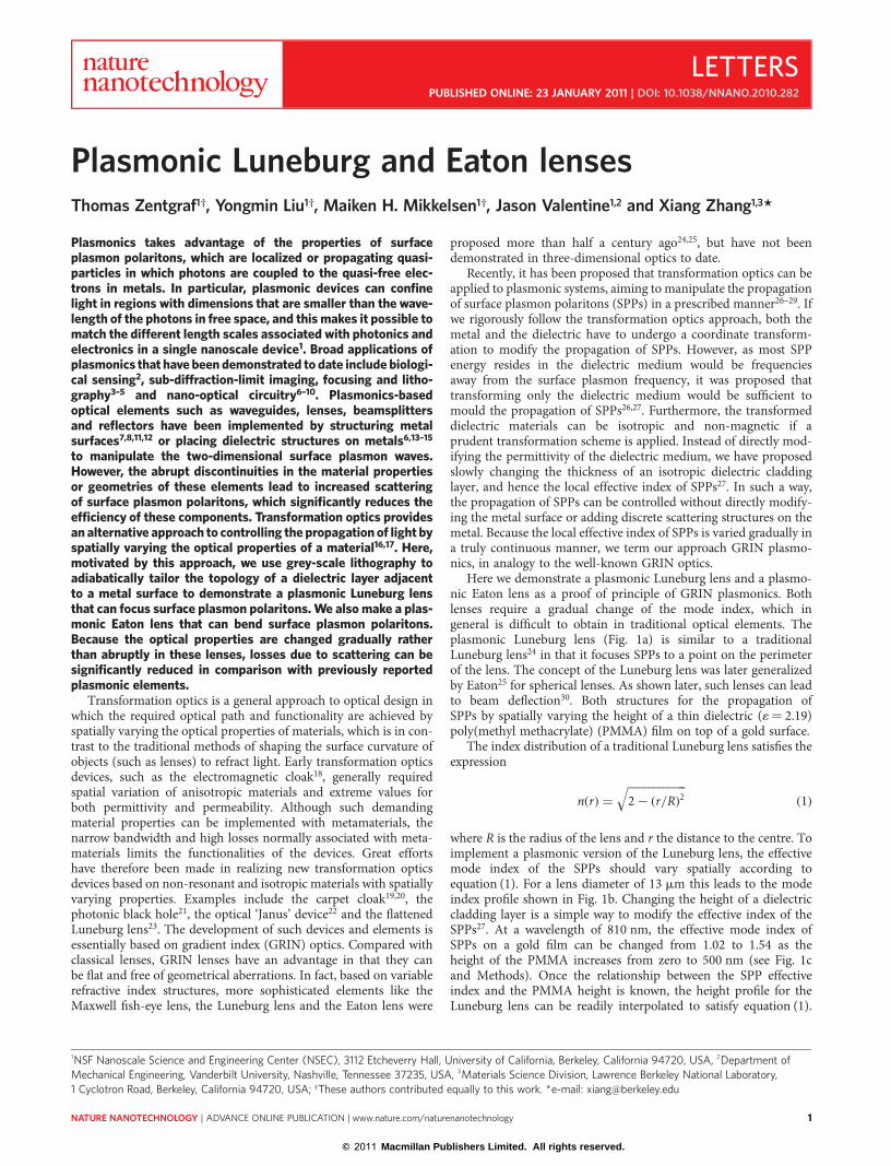
where R is the radius of the lens and r the distance to the centre. Toimplement a plasmonic version of the Luneburg lens, the effectivemode index of the SPPs should vary spatially according toequation (1). For a lens diameter of 13 mm this leads to the modeindex profile shown in Fig. 1b. Changing the height of a dielectriccladding layer is a simple way to modify the effective index of theSPPs27. At a wavelength of 810 nm, the effective mode index ofSPPs on a gold film can be changed from 1.02 to 1.54 as theheight of the PMMA increases from zero to 500 nm (see Fig. 1cand Methods). Once the relationship between the SPP effectiveindex and the PMMA height is known, the height profile for theLuneburg lens can be readily interpolated to satisfy equation (1).
1NSF Nanoscale Science and Engineering Center (NSEC), 3112 Etcheverry Hall, University of California, Berkeley, California 94720, USA, 2Department ofMechanical Engineering, Vanderbilt University, Nashville, Tennessee 37235, USA, 3Materials Science Division, Lawrence Berkeley National Laboratory,1 Cyclotron Road, Berkeley, California 94720, USA; †These authors contributed equally to this work. *e-mail: [email protected]
LETTERSPUBLISHED ONLINE: 23 JANUARY 2011 | DOI: 10.1038/NNANO.2010.282
NATURE NANOTECHNOLOGY | ADVANCE ONLINE PUBLICATION | www.nature.com/naturenanotechnology 1
© 2011 Macmillan Publishers Limited. All rights reserved.
Based on the local height profile of the PMMA structure measuredby atomic force microscopy (AFM), we performed an additionalthree-dimensional full wave simulation (COMSOL Multiphysics)to verify the theoretical performance of the Luneburg lens. Theresult is shown in Fig. 1d, where SPPs launched from the left-hand side can indeed be focused to a point on the perimeter ofthe dielectric cone base. In addition, the gradual change of themode index (impedance matching) reduces the scattering lossof SPPs and the reflections from element boundaries inherent todiscrete structured elements by at least one order of magnitude.
Grey-scale electron beam lithography (EBL) was used to spatiallyvary the PMMA height profile. In this manner, the electron dose iscontinually varied across the sample to modulate the height of thePMMA layer and thus the mode index of SPPs. Fluorescenceimaging31 and leakage radiation microscopy32 were applied tocharacterize the performance of the lenses (see Methods).
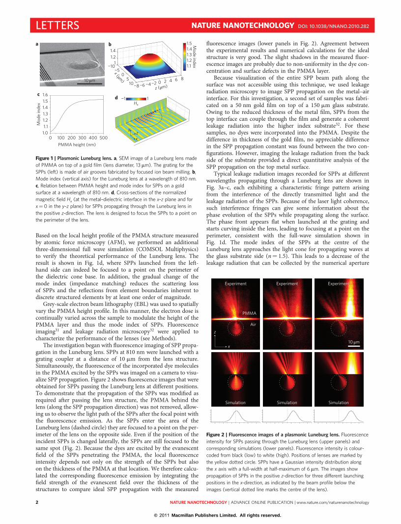
The investigation began with fluorescence imaging of SPP propa-gation in the Luneburg lens. SPPs at 810 nm were launched with agrating coupler at a distance of 10 mm from the lens structure.Simultaneously, the fluorescence of the incorporated dye moleculesin the PMMA excited by the SPPs was imaged on a camera to visu-alize SPP propagation. Figure 2 shows fluorescence images that wereobtained for SPPs passing the Luneburg lens at different positions.To demonstrate that the propagation of the SPPs was modified asrequired after passing the lens structure, the PMMA behind thelens (along the SPP propagation direction) was not removed, allow-ing us to observe the light path of the SPPs after the focal point withthe fluorescence emission. As the SPPs enter the area of theLuneburg lens (dashed circle) they are focused to a point on the per-imeter of the lens on the opposite side. Even if the position of theincident SPPs is changed laterally, the SPPs are still focused to thesame spot (Fig. 2). Because the dyes are excited by the evanescentfield of the SPPs penetrating the PMMA, the local fluorescenceintensity depends not only on the strength of the SPPs but alsoon the thickness of the PMMA at that location. We therefore calcu-lated the corresponding fluorescence emission by integrating thefield strength of the evanescent field over the thickness of thestructures to compare ideal SPP propagation with the measured
fluorescence images (lower panels in Fig. 2). Agreement betweenthe experimental results and numerical calculations for the idealstructure is very good. The slight shadows in the measured fluor-escence images are probably due to non-uniformity in the dye con-centration and surface defects in the PMMA layer.
Because visualization of the entire SPP beam path along thesurface was not accessible using this technique, we used leakageradiation microscopy to image SPP propagation on the metal–airinterface. For this investigation, a second set of samples was fabri-cated on a 50 nm gold film on top of a 150 mm glass substrate.Owing to the reduced thickness of the metal film, SPPs from thetop interface can couple through the film and generate a coherentleakage radiation into the higher index substrate32. For thesesamples, no dyes were incorporated into the PMMA. Despite thedifference in thickness of the gold film, no appreciable differencein the SPP propagation constant was found between the two con-figurations. However, imaging the leakage radiation from the backside of the substrate provided a direct quantitative analysis of theSPP propagation on the top metal surface.
Typical leakage radiation images recorded for SPPs at differentwavelengths propagating through a Luneburg lens are shown inFig. 3a–c, each exhibiting a characteristic fringe pattern arisingfrom the interference of the directly transmitted light and theleakage radiation of the SPPs. Because of the laser light coherence,such interference fringes can give some information about thephase evolution of the SPPs while propagating along the surface.The phase front appears flat when launched at the grating andstarts curving inside the lens, leading to focusing at a point on theperimeter, consistent with the full-wave simulation shown inFig. 1d. The mode index of the SPPs at the centre of theLuneburg lens approaches the light cone for propagating waves atthe glass substrate side (n¼ 1.5). This leads to a decrease of theleakage radiation that can be collected by the numerical aperture
10 µm
a
c
0 100 200 300 400 5001.01.11.21.31.41.51.6
Mod
e in
dex
PMMA height (nm)
b
−8 −6 −4−2 0 2 4 6 810
50
−5−10
11.21.4
x (µm)
z (µm)
1.11.21.31.41.5 M
ode index
xz
y
−1 1Hx
d
Figure 1 | Plasmonic Luneburg lens. a, SEM image of a Luneburg lens made
of PMMA on top of a gold film (lens diameter, 13mm). The grating for the
SPPs (left) is made of air grooves fabricated by focused ion beam milling. b,
Mode index (vertical axis) for the Luneburg lens at a wavelength of 810 nm.
c, Relation between PMMA height and mode index for SPPs on a gold
surface at a wavelength of 810 nm. d, Cross-sections of the normalized
magnetic field Hx (at the metal–dielectric interface in the x–z plane and for
x¼0 in the y–z plane) for SPPs propagating through the Luneburg lens in
the positive z-direction. The lens is designed to focus the SPPs to a point on
the perimeter of the lens.
x
z
Simulation
Experiment
Simulation
Experiment
Simulation
Experiment
PMMA
Air
10 µm
Figure 2 | Fluorescence images of a plasmonic Luneburg lens. Fluorescence
intensity for SPPs passing through the Luneburg lens (upper panels) and
corresponding simulations (lower panels). Fluorescence intensity is colour-
coded from black (low) to white (high). Positions of lenses are marked by
the yellow dotted circle. SPPs have a Gaussian intensity distribution along
the x axis with a full-width at half-maximum of 6 mm. The images show
propagation of SPPs in the positive z-direction for three different launching
positions in the x-direction, as indicated by the beam profile below the
images (vertical dotted line marks the centre of the lens).
LETTERS NATURE NANOTECHNOLOGY DOI: 10.1038/NNANO.2010.282
NATURE NANOTECHNOLOGY | ADVANCE ONLINE PUBLICATION | www.nature.com/naturenanotechnology2
© 2011 Macmillan Publishers Limited. All rights reserved.
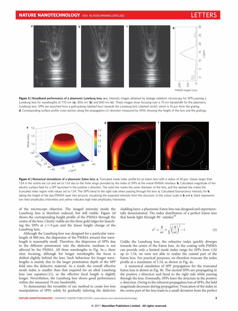
of the microscope objective. The imaged intensity inside theLuneburg lens is therefore reduced, but still visible. Figure 3dshows the corresponding height profile of the PMMA through thecentre of the lens. Clearly visible are the three gold ridges for launch-ing the SPPs at z¼ 0 mm and the linear height change of theLuneburg lens.
Although the Luneburg lens was designed for a particular wave-length of 800 nm, the dispersion of the PMMA around this wave-length is reasonably small. Therefore, the dispersion of SPPs dueto the different penetration into the dielectric medium is notaffected by the PMMA. All three wavelengths in Fig. 3a–c showclear focusing, although for longer wavelengths the focus isshifted slightly behind the lens. Such behaviour for longer wave-lengths is mainly due to the larger penetration depth of the SPPfield into the dielectric material. As a result, the overall effectivemode index is smaller than that required for an ideal Luneburglens (see equation (1)), so the effective focal length is slightlylonger. Nevertheless, the Luneburg lens shows good performancewithin the measured 70 nm bandwidth.
To demonstrate the versatility of our method to create low-lossmanipulation of SPPs solely by gradually tailoring the dielectric
cladding layer, a plasmonic Eaton lens was designed and experimen-tally demonstrated. The index distribution of a perfect Eaton lensthat bends light through 908 satisfies30
n2 = Rnr
+
�����������Rnr
( )2
−1
√(2)
Unlike the Luneburg lens, the refractive index quickly divergestowards the centre of the Eaton lens. As the coating with PMMAcan provide only a limited mode index range for SPPs from 1.02up to 1.54, we were not able to realize the central part of theEaton lens. For practical purposes, we therefore truncate the indexprofile at a maximum of 1.54, as shown in Fig. 4a.
A numerical simulation of SPP propagation for the truncatedEaton lens is shown in Fig. 4b. The excited SPPs are propagating inthe positive z-direction and bend to the right side while passingthrough the lens. Eventually, SPPs leave the structure in the positivex-direction. Owing to the inherent propagation loss of SPPs, the fieldmagnitude decreases during propagation. Truncation of the index inthe centre part of the lens leads to a small deviation from the perfect
x
z
Focus
Lens
a b c
05
1015
2025
300
100
200
PMMA height (nm)
z (µ
m)
d
Figure 3 | Broadband performance of a plasmonic Luneburg lens. a–c, Intensity images obtained by leakage radiation microscopy for SPPs passing a
Luneburg lens for wavelengths of 770 nm (a), 800 nm (b) and 840 nm (c). These images show focusing over a 70 nm bandwidth for the plasmonic
Luneburg lens. SPPs are launched from a gold grating (dashed box) towards the Luneburg lens (dashed circle), which is 10 mm from the grating.
d, Corresponding surface profile cross-section along the propagation (z) direction measured by AFM, showing the height of the lens and the gratings.
cb
x
z
x
z
−40 −20 0 20 4020
−40
0−20
40
1
1.4
1.6
x (µm)
z (µm)
1.2
Mod
e in
dex
1.1
1.2
1.3
1.4
1.5a
Figure 4 | Numerical simulations of a plasmonic Eaton lens. a, Truncated mode index profile for an Eaton lens with a radius of 30 mm. Values larger than
1.54 in the centre are cut and set to 1.54 due to the finite range provided by the index of SPPs at the metal–PMMA interface. b, Calculated magnitude of the
electric surface field for a SPP launched in the positive z-direction. The solid line marks the outer diameter of the lens, and the dashed line marks the
truncated index region with values set to 1.54. The SPPs bend to the right side when passing through the lens. c, Calculated fluorescence intensity for b,
taking the height of the dye/PMMA layer into account, visualizing the expected intensity from the structure. In the colour scale in b and c, black represents
low field amplitudes/intensities and yellow indicates high field amplitudes/intensities.
NATURE NANOTECHNOLOGY DOI: 10.1038/NNANO.2010.282 LETTERS
NATURE NANOTECHNOLOGY | ADVANCE ONLINE PUBLICATION | www.nature.com/naturenanotechnology 3
© 2011 Macmillan Publishers Limited. All rights reserved.
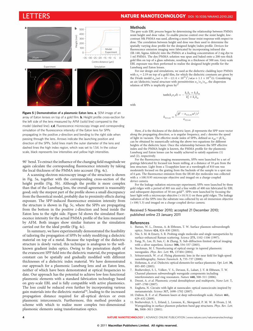
908 bend. To extract the influence of the changing field magnitude weagain calculate the corresponding fluorescence intensity by takingthe local thickness of the PMMA into account (Fig. 4c).
A scanning electron microscopy image of the structure is shownin Fig. 5a, together with the corresponding cross-section of theheight profile (Fig. 5b). Although the profile is more complexthan that of the Luneburg lens, the overall agreement is reasonablygood; only the steepest part of the profile shows a small discrepancyfrom the theoretical model, probably due to proximity effects duringexposure. The SPP-induced fluorescence emission intensity fromthe structure is shown in Fig. 5c, where the SPPs are propagatingfrom the bottom in the positive z-direction and bend inside theEaton lens to the right side. Figure 5d shows the simulated fluor-escence intensity for the actual PMMA profile of the lens measuredby AFM. Both images show similar features as the simulationcarried out for the ideal profile (Fig. 4c).
In summary, we have experimentally demonstrated the feasibilityof tailoring the propagation of SPPs by solely modifying a dielectricmaterial on top of a metal. Because the topology of the dielectricstructure is slowly varied, this technique is analogous to the well-known gradient index optics. Owing to the penetration depth ofthe evanescent SPP field into the dielectric material, the propagationconstant can be spatially and gradually modified with differentthicknesses of a dielectric index material. We have demonstratedour approach for a plasmonic Luneburg lens and an Eaton lens,neither of which have been demonstrated at optical frequencies todate. Our approach has the potential to achieve low-loss functionalplasmonic elements with a standard fabrication technology basedon grey-scale EBL and is fully compatible with active plasmonics.The loss could be reduced even further by incorporating variousgain materials into the dielectric material34, leading to the increasedpropagation distance required for all-optical devices or evenplasmonic interconnects. Furthermore, this method provides ascheme with which to realize more complex two-dimensionalplasmonic elements using transformation optics.
MethodsThe grey-scale EBL process began by determining the relationship between PMMAresist height and dose value. To enable precise control over the resist height, low-contrast 50k PMMA was used, allowing a more linear resist response with respect todose. The correlation between height and dose was then used to determine thespatially varying dose profile for the designed height/index profile. Devices forfluorescence emission imaging were fabricated by incorporating infrared dye(IR-140, Sigma Aldrich) into the PMMA at a loading concentration of 2 mg dye to1 ml PMMA. The dye/PMMA solution was spun and baked onto a 200-nm-thickgold film on top of a glass substrate, resulting in a thickness of 500 nm. Grey-scaleEBL exposure was then performed to realize the designed height profile for theLuneburg and Eaton lenses.
For our design and simulations, we used as the dielectric cladding layer PMMAwith 12¼ 2.19 on top of a gold film, for which the dielectric constants are given bythe Drude model 1m(v) = 10 − ((1.4 × 10¹⁶)2/v(v+ 1.1 × 10¹⁴i)). Consideringan air/dielectric/metal structure with permittivities 11/12/1m , the dispersionrelation of SPPs is implicitly given by27
tanh(k212d) = − k1k2 + k2km
k22 + k1km
with
k1(2,m) =
�������������������b2 − 11(2,m)v
2/c2√
11(2,m)
Here, d is the thickness of the dielectric layer, b represents the SPP wave vectoralong the propagating direction, v is angular frequency, and c denotes the speedof light in vacuum. The effective mode index of SPPs, defined as neff¼ b/k0,can be obtained by numerically solving the above two equations for differentheights of the dielectric layer. Once the relationship between the SPP effectiveindex and the PMMA height is known, the PMMA profile for the plasmonicLuneburg and Eaton lenses can be readily achieved to satisfy equations (1)and (2), respectively.
For the fluorescence imaging measurements, SPPs were launched by a set ofgratings fabricated by focused ion beam milling, at a distance of 10 mm from thelens structure. Light from a Ti:sapphire laser at a wavelength of 810 nm wasmoderately focused on the grating from the backside of the sample to a spot sizeof 6 mm. The fluorescence emission from the IR140 dye molecules was collectedwith a ×100/0.95 microscope objective and imaged on a charge-coupleddevice camera.
For the leakage radiation microscopy experiment, SPPs were launched by threegold ridges with a period of 805 nm and a line width of 400 nm fabricated by EBLand subsequent deposition of 50 nm gold33. SPPs were launched by focusing thelaser light with a microscope objective (×10/0.1) on these gold ridges. The leakageradiation of the SPPs into the substrate was collected by an oil immersion objective(×100/1.3) and imaged on a charge-coupled device camera.
Received 5 November 2010; accepted 21 December 2010;published online 23 January 2011
References1. Barnes, W. L., Dereux, A. & Ebbesen, T. W. Surface plasmon subwavelength
optics. Nature 424, 824–830 (2003).2. Nie, S. M. & Emery, S. R. Probing single molecules and single nanoparticles by
surface-enhanced Raman scattering. Science 275, 1102–1106 (1997).3. Fang, N., Lee, H, Sun, C. & Zhang, X. Sub-diffraction-limited optical imaging
with a silver superlens. Science 308, 534–537 (2005).4. Stockman, M. I. Nanofocusing of optical energy in tapered plasmonic
waveguides. Phys. Rev. Lett. 93, 137404 (2004).5. Srituravanich, W. et al. Flying plasmonic lens in the near field for high-speed
nanolithography, Nature Nanotech. 3, 733–737 (2008).6. Hohenau, A. et al. Dielectric optical elements for surface plasmons. Opt. Lett. 30,
893–895 (2005).7. Bozhevolnyi, S. I., Volkov, V. S., Devaux, E., Laluet, J.-Y. & Ebbesen, T. W.
Channel plasmon subwavelength waveguide components includinginterferometers and ring resonators. Nature 440, 508–511 (2006).
8. Drezet, A. et al. Plasmonic crystal demultiplexer and multiports. Nano Lett. 7,1697–1700 (2007).
9. Engheta, N. Circuits with light at nanoscales: optical nanocircuits inspired bymetamaterials. Science 317, 1698–1702 (2007).
10. Oulton, R. F. et al. Plasmon lasers at deep subwavelength scale. Nature 461,629–632 (2009).
11. Bozhevolnyi, S. I., Erland, J., Leosson, K., Skovgaard, P. M. W. & Hvam, J. M.Waveguiding in surface plasmon polariton band gap structures. Phys. Rev. Lett.86, 3008–3011 (2001).
20 µm
a
x
z
Experimentc
Simulationd
−35 −30 −25 −20 −15 −10 −5 0
0
100
200
300
400
500
Hei
ght (
nm)
Centre distance (µm)
ExperimentModel
b
Figure 5 | Demonstration of a plasmonic Eaton lens. a, SEM image of an
array of Eaton lenses on top of a gold film. b, Height profile cross-section for
the left side of the lens measured by AFM (solid line) compared to the
model (dashed line). c,d, Fluorescence microscopy image and corresponding
simulation of the fluorescence intensity of the Eaton lens for SPPs
propagating in the positive z-direction and bending to the right side when
passing through the lens. Arrows indicate the launching position and
direction of the SPPs. Solid lines mark the outer diameter of the lens and
dashed lines the high index region, which was set to 1.54. In the colour
scale, black represents low intensities and yellow high intensities.
LETTERS NATURE NANOTECHNOLOGY DOI: 10.1038/NNANO.2010.282
NATURE NANOTECHNOLOGY | ADVANCE ONLINE PUBLICATION | www.nature.com/naturenanotechnology4
© 2011 Macmillan Publishers Limited. All rights reserved.

12. Ditlbacher, H., Krenn, J. R., Schider, G., Leitner, A. & Aussenegg, F. R.Two-dimensional optics with surface plasmon polaritons. Appl. Phys. Lett. 81,1762–1764 (2002).
13. Smolyaninov, I. I., Elliott, J., Zayats, A. V. & Davis, C. C. Far-field opticalmicroscopy with a nanometer-scale resolution based on the in-plane imagemagnification by surface plasmon polaritons. Phys. Rev. Lett. 94, 057401 (2005).
14. Devaux, E. et al. Refractive micro-optical elements for surface plasmons: fromclassical to gradient index optics. Opt. Express 18, 20610–20619 (2010).
15. Smolyaninov, I. I. Transformational optics of plasmonic metamaterials. New J.Phys. 10, 115033 (2008).
16. Pendry, J. B., Schurig, D. & Smith, D. R. Controlling electromagnetic fields.Science 312, 1780–1782 (2006).
17. Leonhardt, U. Optical conformal mapping. Science 312, 1777–1780 (2006).18. Schurig, D. et al. Metamaterial electromagnetic cloak at microwave frequencies.
Science 314, 977–980 (2006).19. Valentine, J., Li, J., Zentgraf, T., Bartal, G. & Zhang, X. An optical cloak made of
dielectrics. Nature Mater. 8, 568–571 (2009).20. Gabrielli, L. H., Cardenas, J., Poitras, C. B. & Lipson, M. Silicon nanostructure
cloak operating at optical frequencies. Nature Photon. 43, 461–463 (2009).21. Cheng, Q., Cui, T. J., Jiang, W. X. & Cai, B. G. An omnidirectional
electromagnetic absorber made of metamaterials. New J. Phys. 12,063006 (2010).
22. Zentgraf, T., Valentine, J., Tapia, N., Li, J. & Zhang, X. An optical ‘Janus’ devicefor integrated photonics. Adv. Mater. 22, 2561–2564 (2010).
23. Kundtz, N. & Smith, D. R. Extreme-angle broadband metamaterial lens.Nature Mater. 9, 129–132 (2010).
24. Luneburg, R. Mathematical Theory of Optics (Brown University, 1944).25. Eaton, J. E. On spherically symmetric lenses. Trans. IRE Antennas Propag. 4,
66–71 (1952).26. Huidobro, P. A., Nesterov, M. L., Martı́n-Moreno, L. & Garcı́a-Vidal, F. J.
Transformation optics for plasmonics. Nano Lett. 10, 1985–1990 (2010).27. Liu, Y., Zentgraf, T., Bartal, G. & Zhang, X. Transformational plasmon optics.
Nano Lett. 10, 1991–1997 (2010).
28. Renger, J. et al. Hidden progress: broadband plasmonic invisibility. Opt. Express18, 15757–15768 (2010).
29. Aubry, A. et al. Plasmonic light-harvesting devices over the whole visiblespectrum. Nano Lett. 10, 2574–2579 (2010).
30. Danner, A. J. & Leonhardt, U. Lossless design of an Eaton lens and invisiblesphere by transformation optics with no bandwidth limitation Conference onLasers and Electro-Optics (CLEO), Baltimore, MD, USA, 31 May–5 June 2009.
31. Ditlbacher, H. et al. Fluorescence imaging of surface plasmon fields. Appl. Phys.Lett. 80, 404–406 (2002).
32. Drezet, A. et al. Leakage radiation microscopy of surface plasmon polaritons.Mater. Sci. Eng. B 149, 220–229 (2008).
33. Radko, I. P. et al. Effciency of local surface plasmon polariton excitation onridges. Phys. Rev. B 78, 115115 (2008).
34. De Leon, I. & Berini, P. Amplification of long-range surface plasmons by adipolar gain medium. Nature Photon. 4, 382–387 (2010).
AcknowledgementsThe authors acknowledge funding support from the US Army Research Office (MURIprogramme W911NF-09-1-0539) and the US National Science Foundation (NSFNanoscale Science and Engineering Center CMMI-0751621).
Author contributionsT.Z., Y.L. and J.V. conceived and designed the experiments. T.Z. and M.H.M. performed theexperiments and analysed the data. Y.L. designed the structures and performed thenumerical simulations. J.V. and M.H.M. fabricated the samples. X.Z. guided the theoreticaland experimental work. All authors discussed the results and co-wrote the manuscript.
Additional informationThe authors declare no competing financial interests. Reprints and permission information isavailable online at http://npg.nature.com/reprintsandpermissions/. Correspondence andrequests for materials should be addressed to X.Z.
NATURE NANOTECHNOLOGY DOI: 10.1038/NNANO.2010.282 LETTERS
NATURE NANOTECHNOLOGY | ADVANCE ONLINE PUBLICATION | www.nature.com/naturenanotechnology 5
© 2011 Macmillan Publishers Limited. All rights reserved.