pic16f72 data sheet - microchip.com · pic16f72 data sheet - microchip.com ... pic16f72
TRANSCRIPT
© 2007 Microchip Technology Inc. DS39597C
PIC16F72Data Sheet
28-Pin, 8-Bit CMOS FLASHMicrocontoller with A/D Converter

Note the following details of the code protection feature on Microchip devices:
• Microchip products meet the specification contained in their particular Microchip Data Sheet.
• Microchip believes that its family of products is one of the most secure families of its kind on the market today, when used in the intended manner and under normal conditions.
• There are dishonest and possibly illegal methods used to breach the code protection feature. All of these methods, to our knowledge, require using the Microchip products in a manner outside the operating specifications contained in Microchip’s Data Sheets. Most likely, the person doing so is engaged in theft of intellectual property.
• Microchip is willing to work with the customer who is concerned about the integrity of their code.
• Neither Microchip nor any other semiconductor manufacturer can guarantee the security of their code. Code protection does not mean that we are guaranteeing the product as “unbreakable.”
Code protection is constantly evolving. We at Microchip are committed to continuously improving the code protection features of ourproducts. Attempts to break Microchip’s code protection feature may be a violation of the Digital Millennium Copyright Act. If such actsallow unauthorized access to your software or other copyrighted work, you may have a right to sue for relief under that Act.
Information contained in this publication regarding deviceapplications and the like is provided only for your convenienceand may be superseded by updates. It is your responsibility toensure that your application meets with your specifications.MICROCHIP MAKES NO REPRESENTATIONS ORWARRANTIES OF ANY KIND WHETHER EXPRESS ORIMPLIED, WRITTEN OR ORAL, STATUTORY OROTHERWISE, RELATED TO THE INFORMATION,INCLUDING BUT NOT LIMITED TO ITS CONDITION,QUALITY, PERFORMANCE, MERCHANTABILITY ORFITNESS FOR PURPOSE. Microchip disclaims all liabilityarising from this information and its use. Use of Microchipdevices in life support and/or safety applications is entirely atthe buyer’s risk, and the buyer agrees to defend, indemnify andhold harmless Microchip from any and all damages, claims,suits, or expenses resulting from such use. No licenses areconveyed, implicitly or otherwise, under any Microchipintellectual property rights.
DS39597C-page ii
Trademarks
The Microchip name and logo, the Microchip logo, Accuron, dsPIC, KEELOQ, microID, MPLAB, PIC, PICmicro, PICSTART, PRO MATE, PowerSmart, rfPIC and SmartShunt are registered trademarks of Microchip Technology Incorporated in the U.S.A. and other countries.
AmpLab, FilterLab, Migratable Memory, MXDEV, MXLAB, SEEVAL, SmartSensor and The Embedded Control Solutions Company are registered trademarks of Microchip Technology Incorporated in the U.S.A.
Analog-for-the-Digital Age, Application Maestro, CodeGuard, dsPICDEM, dsPICDEM.net, dsPICworks, ECAN, ECONOMONITOR, FanSense, FlexROM, fuzzyLAB, In-Circuit Serial Programming, ICSP, ICEPIC, Linear Active Thermistor, Mindi, MiWi, MPASM, MPLIB, MPLINK, PICkit, PICDEM, PICDEM.net, PICLAB, PICtail, PowerCal, PowerInfo, PowerMate, PowerTool, REAL ICE, rfLAB, rfPICDEM, Select Mode, Smart Serial, SmartTel, Total Endurance, UNI/O, WiperLock and ZENA are trademarks of Microchip Technology Incorporated in the U.S.A. and other countries.
SQTP is a service mark of Microchip Technology Incorporated in the U.S.A.
All other trademarks mentioned herein are property of their respective companies.
© 2007, Microchip Technology Incorporated, Printed in the U.S.A., All Rights Reserved.
Printed on recycled paper.
Microchip received ISO/TS-16949:2002 certification for its worldwide headquarters, design and wafer fabrication facilities in Chandler and Tempe, Arizona, Gresham, Oregon and Mountain View, California. The Company’s quality system processes and procedures are for its PIC®
MCUs and dsPIC DSCs, KEELOQ® code hopping devices, Serial EEPROMs, microperipherals, nonvolatile memory and analog products. In addition, Microchip’s quality system for the design and manufacture of development systems is ISO 9001:2000 certified.
© 2007 Microchip Technology Inc.
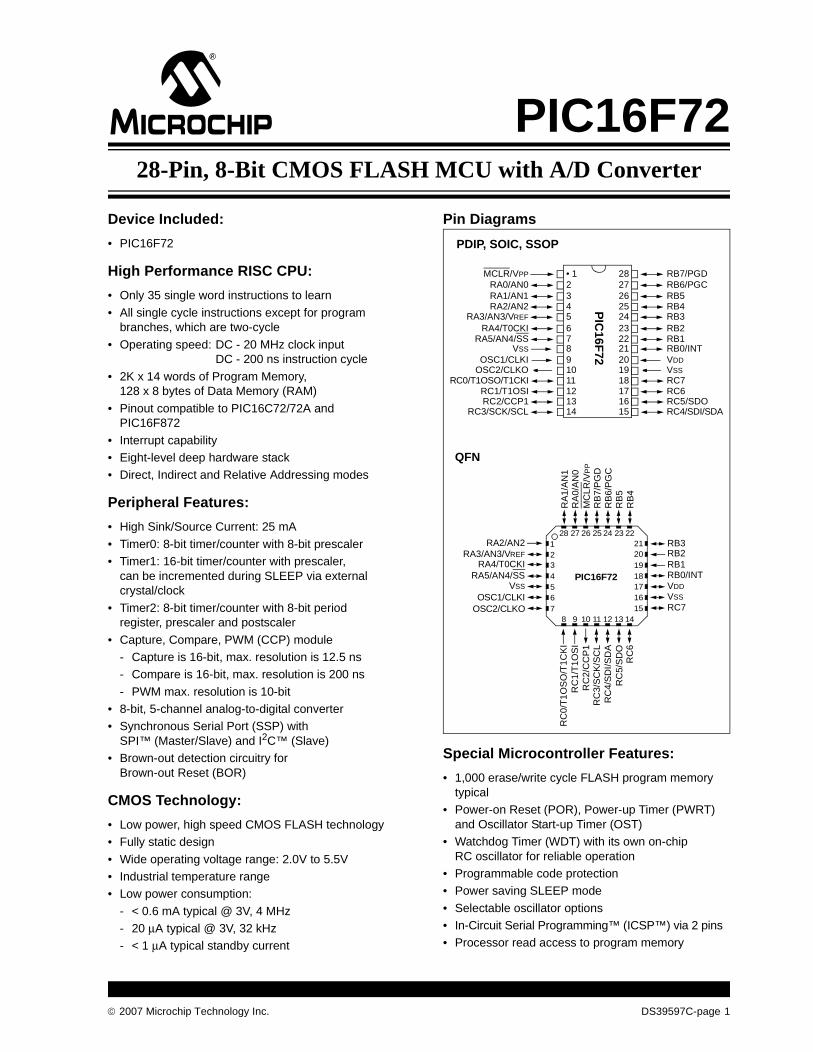
PIC16F7228-Pin, 8-Bit CMOS FLASH MCU with A/D Converter
Device Included:
• PIC16F72
High Performance RISC CPU:
• Only 35 single word instructions to learn
• All single cycle instructions except for program branches, which are two-cycle
• Operating speed: DC - 20 MHz clock inputDC - 200 ns instruction cycle
• 2K x 14 words of Program Memory, 128 x 8 bytes of Data Memory (RAM)
• Pinout compatible to PIC16C72/72A and PIC16F872
• Interrupt capability• Eight-level deep hardware stack• Direct, Indirect and Relative Addressing modes
Peripheral Features:
• High Sink/Source Current: 25 mA
• Timer0: 8-bit timer/counter with 8-bit prescaler• Timer1: 16-bit timer/counter with prescaler,
can be incremented during SLEEP via external crystal/clock
• Timer2: 8-bit timer/counter with 8-bit period register, prescaler and postscaler
• Capture, Compare, PWM (CCP) module- Capture is 16-bit, max. resolution is 12.5 ns- Compare is 16-bit, max. resolution is 200 ns
- PWM max. resolution is 10-bit• 8-bit, 5-channel analog-to-digital converter• Synchronous Serial Port (SSP) with
SPI™ (Master/Slave) and I2C™ (Slave)• Brown-out detection circuitry for
Brown-out Reset (BOR)
CMOS Technology:
• Low power, high speed CMOS FLASH technology• Fully static design
• Wide operating voltage range: 2.0V to 5.5V• Industrial temperature range• Low power consumption:
- < 0.6 mA typical @ 3V, 4 MHz- 20 μA typical @ 3V, 32 kHz- < 1 μA typical standby current
Pin Diagrams
Special Microcontroller Features:
• 1,000 erase/write cycle FLASH program memory typical
• Power-on Reset (POR), Power-up Timer (PWRT) and Oscillator Start-up Timer (OST)
• Watchdog Timer (WDT) with its own on-chip RC oscillator for reliable operation
• Programmable code protection• Power saving SLEEP mode
• Selectable oscillator options• In-Circuit Serial Programming™ (ICSP™) via 2 pins• Processor read access to program memory
MCLR/VPP
RA0/AN0RA1/AN1RA2/AN2
RA3/AN3/VREF
RA4/T0CKIRA5/AN4/SS
VSS
OSC1/CLKIOSC2/CLKO
RC0/T1OSO/T1CKIRC1/T1OSIRC2/CCP1
RC3/SCK/SCL
RB7/PGDRB6/PGCRB5RB4RB3RB2RB1RB0/INTVDDVSSRC7RC6RC5/SDORC4/SDI/SDA
• 1234567891011121314
2827262524232221201918171615
PDIP, SOIC, SSOP
QFN
23456
1
7
RA2/AN2RA3/AN3/VREF
RA4/T0CKIRA5/AN4/SS
VSS
OSC1/CLKIOSC2/CLKO 15
161718192021 RB3
RB2RB1RB0/INTVDDVSS
RC7
RC
0/T
1OS
O/T
1CK
IR
C1/
T1O
SI
RC
2/C
CP
1R
C3/
SC
K/S
CL
RC
4/S
DI/S
DA
RC
5/S
DO
RC
6
232425262728 22
RA
1/A
N1
RA
0/A
N0
MC
LR/V
PP
RB
7/P
GD
RB
6/P
GC
RB
5R
B4
10 118 9 12 13 14
PIC16F72
PIC
16F72
© 2007 Microchip Technology Inc. DS39597C-page 1
PIC16F72
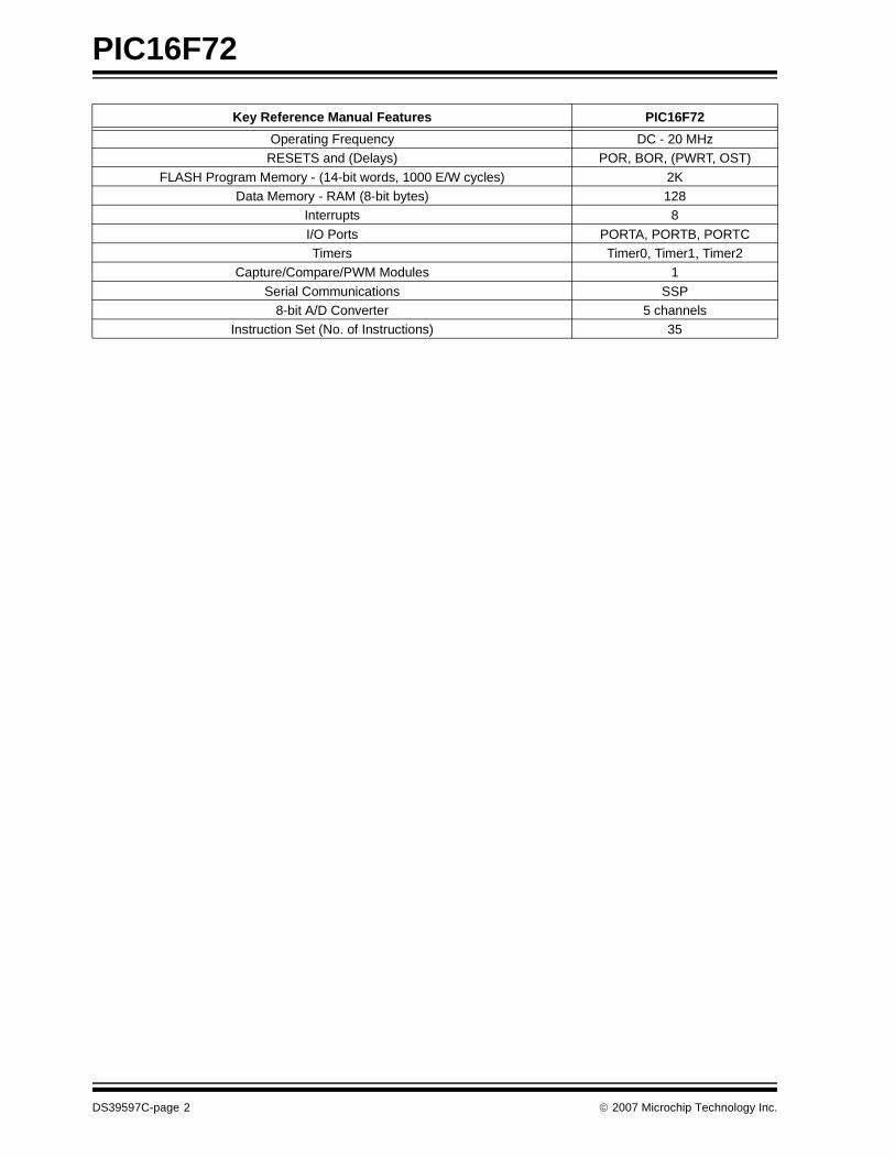
Key Reference Manual Features PIC16F72
Operating Frequency DC - 20 MHzRESETS and (Delays) POR, BOR, (PWRT, OST)
FLASH Program Memory - (14-bit words, 1000 E/W cycles) 2KData Memory - RAM (8-bit bytes) 128
Interrupts 8
I/O Ports PORTA, PORTB, PORTCTimers Timer0, Timer1, Timer2
Capture/Compare/PWM Modules 1
Serial Communications SSP8-bit A/D Converter 5 channels
Instruction Set (No. of Instructions) 35
DS39597C-page 2 © 2007 Microchip Technology Inc.
PIC16F72
Table of Contents
1.0 Device Overview .......................................................................................................................................................................... 52.0 Memory Organization ................................................................................................................................................................... 73.0 I/O Ports ..................................................................................................................................................................................... 214.0 Reading Program Memory ......................................................................................................................................................... 275.0 Timer0 Module ........................................................................................................................................................................... 296.0 Timer1 Module ........................................................................................................................................................................... 317.0 Timer2 Module ........................................................................................................................................................................... 358.0 Capture/Compare/PWM (CCP) Module ..................................................................................................................................... 379.0 Synchronous Serial Port (SSP) Module ..................................................................................................................................... 4310.0 Analog-to-Digital Converter (A/D) Module.................................................................................................................................. 5311.0 Special Features of the CPU...................................................................................................................................................... 5912.0 Instruction Set Summary ............................................................................................................................................................ 7313.0 Development Support................................................................................................................................................................. 8114.0 Electrical Characteristics ............................................................................................................................................................ 8715.0 DC and AC Characteristics Graphs and Tables....................................................................................................................... 10716.0 Package Marking Information................................................................................................................................................... 117Appendix A: Revision History ........................................................................................................................................................ 123Appendix B: Conversion Considerations........................................................................................................................................ 123Index .................................................................................................................................................................................................. 125On-Line Support................................................................................................................................................................................. 131Reader Response .............................................................................................................................................................................. 132Product Identification System ............................................................................................................................................................ 133
TO OUR VALUED CUSTOMERS
It is our intention to provide our valued customers with the best documentation possible to ensure successful use of your Microchipproducts. To this end, we will continue to improve our publications to better suit your needs. Our publications will be refined andenhanced as new volumes and updates are introduced.
If you have any questions or comments regarding this publication, please contact the Marketing Communications Department viaE-mail at [email protected] or fax the Reader Response Form in the back of this data sheet to (480) 792-4150. Wewelcome your feedback.
Most Current Data SheetTo obtain the most up-to-date version of this data sheet, please register at our Worldwide Web site at:
http://www.microchip.com
You can determine the version of a data sheet by examining its literature number found on the bottom outside corner of any page.The last character of the literature number is the version number, (e.g., DS30000A is version A of document DS30000).
ErrataAn errata sheet, describing minor operational differences from the data sheet and recommended workarounds, may exist for currentdevices. As device/documentation issues become known to us, we will publish an errata sheet. The errata will specify the revisionof silicon and revision of document to which it applies.
To determine if an errata sheet exists for a particular device, please check with one of the following:
• Microchip’s Worldwide Web site; http://www.microchip.com• Your local Microchip sales office (see last page)When contacting a sales office, please specify which device, revision of silicon and data sheet (include literature number) you areusing.
Customer Notification SystemRegister on our web site at www.microchip.com to receive the most current information on all of our products.
© 2007 Microchip Technology Inc. DS39597C-page 3

PIC16F72
NOTES:
DS39597C-page 4 © 2007 Microchip Technology Inc.

PIC16F72
1.0 DEVICE OVERVIEW
This document contains device specific information forthe operation of the PIC16F72 device. Additional infor-mation may be found in the PIC™ Mid-Range MCUReference Manual (DS33023), which may be down-loaded from the Microchip website. The ReferenceManual should be considered a complementary docu-ment to this data sheet, and is highly recommendedreading for a better understanding of the device archi-tecture and operation of the peripheral modules.
The PIC16F72 belongs to the Mid-Range family of thePIC devices. A block diagram of the device is shown inFigure 1-1.
The program memory contains 2K words, which trans-late to 2048 instructions, since each 14-bit programmemory word is the same width as each deviceinstruction. The data memory (RAM) contains 128 bytes.
There are 22 I/O pins that are user configurable on apin-to-pin basis. Some pins are multiplexed with otherdevice functions. These functions include:• External interrupt
• Change on PORTB interrupt• Timer0 clock input• Timer1 clock/oscillator
• Capture/Compare/PWM• A/D converter• SPI/I2C
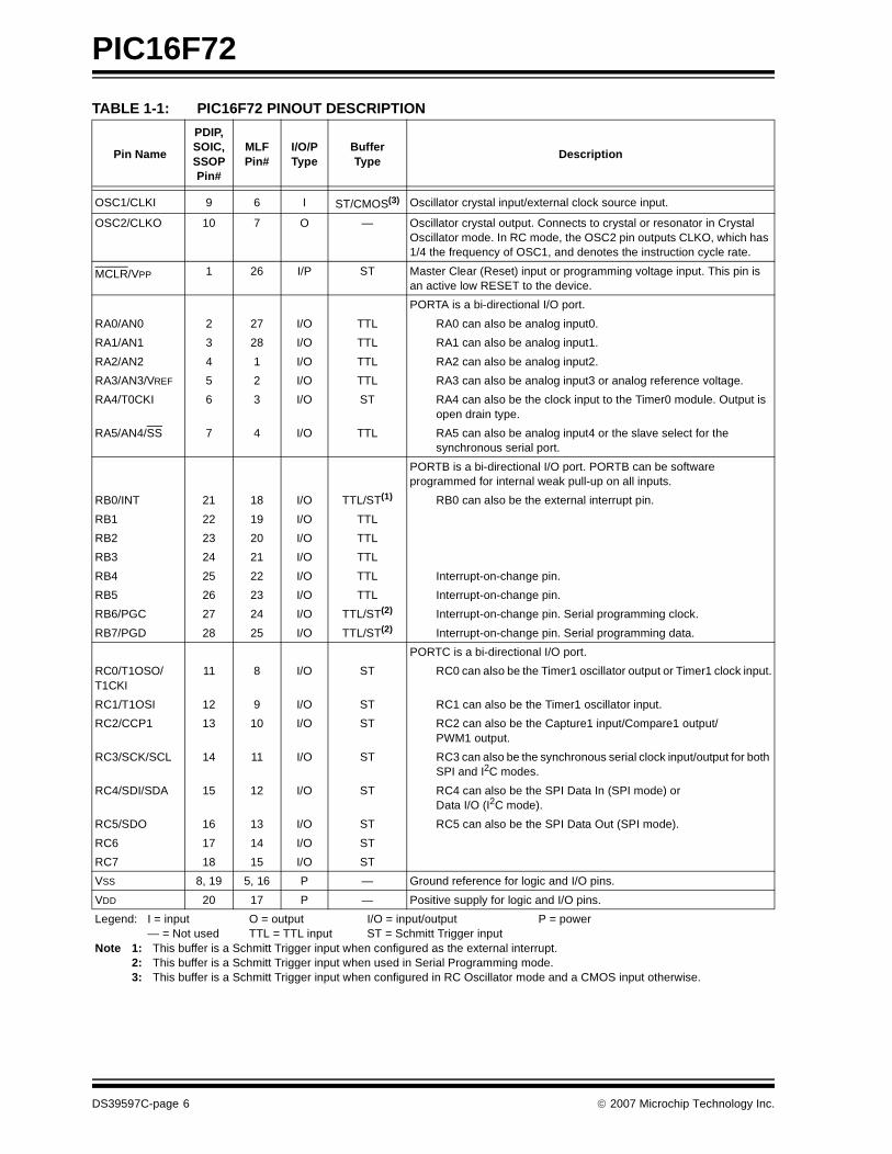
Table 1-1 details the pinout of the device withdescriptions and details for each pin.
FIGURE 1-1: PIC16F72 BLOCK DIAGRAM
FLASH
Memory2K x 14
13 Data Bus 8
14ProgramBus
Instruction reg
Program Counter
8-Level Stack(13-bit)
RAMFile
Registers
128 x 8
Direct Addr 7
RAM Addr(1) 9
Addr MUX
IndirectAddr
FSR reg
STATUS reg
MUX
ALU
W reg
Power-upTimer
OscillatorStart-up Timer
Power-onReset
WatchdogTimer
InstructionDecode &
Control
TimingGeneration
OSC1/CLKIOSC2/CLKO
MCLR VDD, VSS
Timer0
A/DSynchronous
Serial Port
PORTA
PORTCRC0/T1OSO/T1CKIRC1/T1OSIRC2/CCP1RC3/SCK/SCLRC4/SDI/SDARC5/SDORC6RC7
8
8
Brown-outReset
Note 1: Higher order bits are from the STATUS register.
CCP1
Timer1 Timer2
RA4/T0CKIRA5/AN4/SS
RA3/AN3/VREF
RA2/AN2RA1/AN1RA0/AN0
8
3
Program
PORTBRB0/INTRB1RB2RB3RB4RB5RB6/PGCRB7/PGD
© 2007 Microchip Technology Inc. DS39597C-page 5
PIC16F72
TABLE 1-1: PIC16F72 PINOUT DESCRIPTION
Pin Name
PDIP,SOIC,SSOPPin#
MLFPin#
I/O/PType
BufferType
Description
OSC1/CLKI 9 6 I ST/CMOS(3) Oscillator crystal input/external clock source input.
OSC2/CLKO 10 7 O — Oscillator crystal output. Connects to crystal or resonator in Crystal Oscillator mode. In RC mode, the OSC2 pin outputs CLKO, which has 1/4 the frequency of OSC1, and denotes the instruction cycle rate.
MCLR/VPP 1 26 I/P ST Master Clear (Reset) input or programming voltage input. This pin is an active low RESET to the device.
PORTA is a bi-directional I/O port.
RA0/AN0 2 27 I/O TTL RA0 can also be analog input0.
RA1/AN1 3 28 I/O TTL RA1 can also be analog input1.
RA2/AN2 4 1 I/O TTL RA2 can also be analog input2.
RA3/AN3/VREF 5 2 I/O TTL RA3 can also be analog input3 or analog reference voltage.
RA4/T0CKI 6 3 I/O ST RA4 can also be the clock input to the Timer0 module. Output is open drain type.
RA5/AN4/SS 7 4 I/O TTL RA5 can also be analog input4 or the slave select for the synchronous serial port.
PORTB is a bi-directional I/O port. PORTB can be software programmed for internal weak pull-up on all inputs.
RB0/INT 21 18 I/O TTL/ST(1) RB0 can also be the external interrupt pin.
RB1 22 19 I/O TTL
RB2 23 20 I/O TTL
RB3 24 21 I/O TTL
RB4 25 22 I/O TTL Interrupt-on-change pin.
RB5 26 23 I/O TTL Interrupt-on-change pin.
RB6/PGC 27 24 I/O TTL/ST(2) Interrupt-on-change pin. Serial programming clock.
RB7/PGD 28 25 I/O TTL/ST(2) Interrupt-on-change pin. Serial programming data.
PORTC is a bi-directional I/O port.
RC0/T1OSO/T1CKI
11 8 I/O ST RC0 can also be the Timer1 oscillator output or Timer1 clock input.
RC1/T1OSI 12 9 I/O ST RC1 can also be the Timer1 oscillator input.
RC2/CCP1 13 10 I/O ST RC2 can also be the Capture1 input/Compare1 output/PWM1 output.
RC3/SCK/SCL 14 11 I/O ST RC3 can also be the synchronous serial clock input/output for both SPI and I2C modes.
RC4/SDI/SDA 15 12 I/O ST RC4 can also be the SPI Data In (SPI mode) or Data I/O (I2C mode).
RC5/SDO 16 13 I/O ST RC5 can also be the SPI Data Out (SPI mode).
RC6 17 14 I/O ST
RC7 18 15 I/O ST
VSS 8, 19 5, 16 P — Ground reference for logic and I/O pins.
VDD 20 17 P — Positive supply for logic and I/O pins.
Legend: I = input O = output I/O = input/output P = power— = Not used TTL = TTL input ST = Schmitt Trigger input
Note 1: This buffer is a Schmitt Trigger input when configured as the external interrupt.2: This buffer is a Schmitt Trigger input when used in Serial Programming mode.3: This buffer is a Schmitt Trigger input when configured in RC Oscillator mode and a CMOS input otherwise.
DS39597C-page 6 © 2007 Microchip Technology Inc.

PIC16F72
2.0 MEMORY ORGANIZATION
There are two memory blocks in the PIC16F72 device.These are the program memory and the data memory.Each block has separate buses so that concurrentaccess can occur. Program memory and data memoryare explained in this section. Program memory can beread internally by the user code (see Section 7.0).
The data memory can further be broken down into thegeneral purpose RAM and the Special FunctionRegisters (SFRs). The operation of the SFRs thatcontrol the “core” are described here. The SFRs usedto control the peripheral modules are described in thesection discussing each individual peripheral module.
Additional information on device memory may be foundin the PIC™ Mid-Range Reference Manual,(DS33023).
2.1 Program Memory Organization
PIC16F72 devices have a 13-bit program counter capa-ble of addressing a 8K x 14 program memory space.The address range for this program memory is 0000h -07FFh. Accessing a location above the physicallyimplemented address will cause a wraparound.
The RESET Vector is at 0000h and the Interrupt Vectoris at 0004h.
FIGURE 2-1: PROGRAM MEMORY MAP AND STACK
2.2 Data Memory Organization
The Data Memory is partitioned into multiple banks thatcontain the General Purpose Registers and the SpecialFunction Registers. Bits RP1 (STATUS<6>) and RP0(STATUS<5>) are the bank select bits.
Each bank extends up to 7Fh (128 bytes). The lowerlocations of each bank are reserved for the SpecialFunction Registers. Above the Special Function Regis-ters are General Purpose Registers, implemented asstatic RAM.
All implemented banks contain SFRs. Some “high use”SFRs from one bank may be mirrored in another bank,for code reduction and quicker access (e.g., theSTATUS register is in Banks 0 - 3).
2.2.1 GENERAL PURPOSE REGISTER FILE
The register file can be accessed either directly, or indi-rectly, through the File Select Register FSR (seeSection 2.5).
PC<12:0>
13
0000h
0004h0005h
07FFh
1FFFh
Stack Level 1
Stack Level 8
RESET Vector
Interrupt Vector
On-chip ProgramMemory
CALL, RETURNRETFIE, RETLW
0800h
Use
r M
emor
yS
pace
RP1:RP0 Bank
00 0
01 1
10 2
11 3
© 2007 Microchip Technology Inc. DS39597C-page 7

PIC16F72
FIGURE 2-2: PIC16F72 REGISTER FILE MAP
Indirect addr.(*)
TMR0PCL
STATUSFSR
PORTAPORTBPORTC
PCLATHINTCON
PIR1
TMR1LTMR1HT1CONTMR2
T2CONSSPBUFSSPCONCCPR1LCCPR1H
CCP1CON
OPTIONPCL
STATUSFSR
TRISATRISBTRISC
PCLATHINTCON
PIE1
PCON
PR2
SSPSTAT
00h01h02h03h04h05h06h07h08h09h0Ah0Bh0Ch0Dh0Eh0Fh10h11h12h13h14h15h16h17h18h19h1Ah1Bh1Ch1Dh1Eh1Fh
80h81h82h83h84h85h86h87h88h89h8Ah8Bh8Ch8Dh8Eh8Fh90h91h92h93h94h95h96h97h98h99h9Ah9Bh9Ch9Dh9Eh9Fh
20h A0h
7Fh FFhBank 0 Bank 1
FileAddress
Indirect addr.(*) Indirect addr.(*)
PCLSTATUS
FSR
PCLATHINTCON
PCLSTATUS
FSR
PCLATHINTCON
100h101h102h103h104h105h106h107h108h109h10Ah10Bh
180h181h182h183h184h185h186h187h188h189h18Ah18Bh
17Fh 1FFhBank 2 Bank 3
Indirect addr.(*)
TMR0 OPTION
ADRESADCON0 ADCON1
GeneralPurposeRegister
accesses20h-7Fh
TRISBPORTB
96 Bytes
10Ch10Dh10Eh10Fh110h
18Ch18Dh18Eh18Fh190h
PMDATLPMADRL
PMCON1
PMDATHPMADRH
Unimplemented data memory locations, read as ‘0’. * Not a physical register.
FileAddress
FileAddress
FileAddress
SSPADD
120h
11Fh
1A0h
19Fh
GeneralPurposeRegister
32 Bytes BFhC0h
accesses40h-7Fh
accessesA0h -BFh
1BFh
1C0h
accesses40h -7Fh
DS39597C-page 8 © 2007 Microchip Technology Inc.

PIC16F72
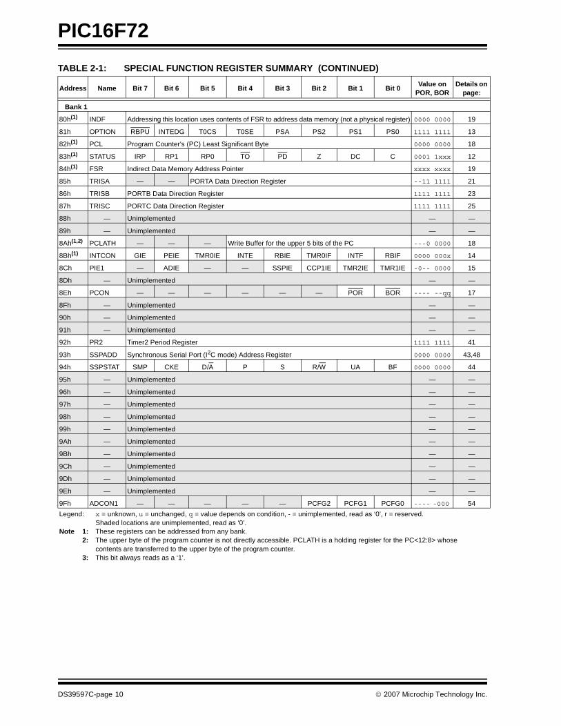
2.2.2 SPECIAL FUNCTION REGISTERS
The Special Function Registers are registers used bythe CPU and peripheral modules for controlling thedesired operation of the device. These registers areimplemented as static RAM. A list of these registers isgiven in Table 2-1.
The Special Function Registers can be classified intotwo sets: core (CPU) and peripheral. Those registersassociated with the core functions are described indetail in this section. Those related to the operation ofthe peripheral features are described in detail in theperipheral feature section.
TABLE 2-1: SPECIAL FUNCTION REGISTER SUMMARY
Address Name Bit 7 Bit 6 Bit 5 Bit 4 Bit 3 Bit 2 Bit 1 Bit 0Value on
POR, BORDetails on
page:
Bank 0
00h(1) INDF Addressing this location uses contents of FSR to address data memory (not a physical register) 0000 0000 19
01h TMR0 Timer0 Module’s Register xxxx xxxx 27,13
02h(1) PCL Program Counter's (PC) Least Significant Byte 0000 0000 18
03h(1) STATUS IRP RP1 RP0 TO PD Z DC C 0001 1xxx 12
04h(1) FSR Indirect Data Memory Address Pointer xxxx xxxx 19
05h PORTA — — PORTA Data Latch when written: PORTA pins when read --0x 0000 21
06h PORTB PORTB Data Latch when written: PORTB pins when read xxxx xxxx 23
07h PORTC PORTC Data Latch when written: PORTC pins when read xxxx xxxx 25
08h — Unimplemented — —
09h — Unimplemented — —
0Ah(1,2) PCLATH — — — Write Buffer for the upper 5 bits of the Program Counter ---0 0000 18
0Bh(1) INTCON GIE PEIE TMR0IE INTE RBIE TMR0IF INTF RBIF 0000 000x 14
0Ch PIR1 — ADIF — — SSPIF CCP1IF TMR2IF TMR1IF -0-- 0000 16
0Dh — Unimplemented — —
0Eh TMR1L Holding Register for the Least Significant Byte of the 16-bit TMR1 Register xxxx xxxx 29
0Fh TMR1H Holding Register for the Most Significant Byte of the 16-bit TMR1 Register xxxx xxxx 29
10h T1CON — — T1CKPS1 T1CKPS0 T1OSCEN T1SYNC TMR1CS TMR1ON --00 0000 29
11h TMR2 Timer2 Module’s Register 0000 0000 33
12h T2CON — TOUTPS3 TOUTPS2 TOUTPS1 TOUTPS0 TMR2ON T2CKPS1 T2CKPS0 -000 0000 34
13h SSPBUF Synchronous Serial Port Receive Buffer/Transmit Register xxxx xxxx 43,48
14h SSPCON WCOL SSPOV SSPEN CKP SSPM3 SSPM2 SSPM1 SSPM0 0000 0000 45
15h CCPR1L Capture/Compare/PWM Register (LSB) xxxx xxxx 38,39,41
16h CCPR1H Capture/Compare/PWM Register (MSB) xxxx xxxx 38,39,41
17h CCP1CON — — CCP1X CCP1Y CCP1M3 CCP1M2 CCP1M1 CCP1M0 --00 0000 37
18h-1Dh — Unimplemented — —
1Eh ADRES A/D Result Register xxxx xxxx 53
1Fh ADCON0 ADCS1 ADCS0 CHS2 CHS1 CHS0 GO/DONE — ADON 0000 00-0 53
Legend: x = unknown, u = unchanged, q = value depends on condition, - = unimplemented, read as ‘0’, r = reserved. Shaded locations are unimplemented, read as ‘0’.
Note 1: These registers can be addressed from any bank.2: The upper byte of the program counter is not directly accessible. PCLATH is a holding register for the PC<12:8> whose
contents are transferred to the upper byte of the program counter.3: This bit always reads as a ‘1’.
© 2007 Microchip Technology Inc. DS39597C-page 9
PIC16F72
Bank 1
80h(1) INDF Addressing this location uses contents of FSR to address data memory (not a physical register) 0000 0000 19
81h OPTION RBPU INTEDG T0CS T0SE PSA PS2 PS1 PS0 1111 1111 13
82h(1) PCL Program Counter's (PC) Least Significant Byte 0000 0000 18
83h(1) STATUS IRP RP1 RP0 TO PD Z DC C 0001 1xxx 12
84h(1) FSR Indirect Data Memory Address Pointer xxxx xxxx 19
85h TRISA — — PORTA Data Direction Register --11 1111 21
86h TRISB PORTB Data Direction Register 1111 1111 23
87h TRISC PORTC Data Direction Register 1111 1111 25
88h — Unimplemented — —
89h — Unimplemented — —
8Ah(1,2) PCLATH — — — Write Buffer for the upper 5 bits of the PC ---0 0000 18
8Bh(1) INTCON GIE PEIE TMR0IE INTE RBIE TMR0IF INTF RBIF 0000 000x 14
8Ch PIE1 — ADIE — — SSPIE CCP1IE TMR2IE TMR1IE -0-- 0000 15
8Dh — Unimplemented — —
8Eh PCON — — — — — — POR BOR ---- --qq 17
8Fh — Unimplemented — —
90h — Unimplemented — —
91h — Unimplemented — —
92h PR2 Timer2 Period Register 1111 1111 41
93h SSPADD Synchronous Serial Port (I2C mode) Address Register 0000 0000 43,48
94h SSPSTAT SMP CKE D/A P S R/W UA BF 0000 0000 44
95h — Unimplemented — —
96h — Unimplemented — —
97h — Unimplemented — —
98h — Unimplemented — —
99h — Unimplemented — —
9Ah — Unimplemented — —
9Bh — Unimplemented — —
9Ch — Unimplemented — —
9Dh — Unimplemented — —
9Eh — Unimplemented — —
9Fh ADCON1 — — — — — PCFG2 PCFG1 PCFG0 ---- -000 54
TABLE 2-1: SPECIAL FUNCTION REGISTER SUMMARY (CONTINUED)
Address Name Bit 7 Bit 6 Bit 5 Bit 4 Bit 3 Bit 2 Bit 1 Bit 0Value on
POR, BORDetails on
page:
Legend: x = unknown, u = unchanged, q = value depends on condition, - = unimplemented, read as ‘0’, r = reserved. Shaded locations are unimplemented, read as ‘0’.
Note 1: These registers can be addressed from any bank.2: The upper byte of the program counter is not directly accessible. PCLATH is a holding register for the PC<12:8> whose
contents are transferred to the upper byte of the program counter.3: This bit always reads as a ‘1’.
DS39597C-page 10 © 2007 Microchip Technology Inc.

PIC16F72
Bank 2
100h(1) INDF Addressing this location uses contents of FSR to address data memory (not a physical register) 0000 0000 19
101h TMR0 Timer0 Module’s Register xxxx xxxx 27
102h(1 PCL Program Counter's (PC) Least Significant Byte 0000 0000 18
103h(1) STATUS IRP RP1 RP0 TO PD Z DC C 0001 1xxx 12
104h(1) FSR Indirect Data Memory Address Pointer xxxx xxxx 19
105h — Unimplemented — —
106h PORTB PORTB Data Latch when written: PORTB pins when read xxxx xxxx 23
107h — Unimplemented — —
108h — Unimplemented — —
109h — Unimplemented — —
10Ah(1,2) PCLATH — — — Write Buffer for the upper 5 bits of the Program Counter ---0 0000 18
10Bh(1) INTCON GIE PEIE TMR0IE INTE RBIE TMR0IF INTF RBIF 0000 000x 14
10Ch PMDATL Data Register Low Byte xxxx xxxx 35
10Dh PMADRL Address Register Low Byte xxxx xxxx 35
10Eh PMDATH — — Data Register High Byte --xx xxxx 35
10Fh PMADRH — — — Address Register High Byte ---x xxxx 35
Bank 3
180h(1) INDF Addressing this location uses contents of FSR to address data memory (not a physical register) 0000 0000 19
181h OPTION RBPU INTEDG T0CS T0SE PSA PS2 PS1 PS0 1111 1111 13
182h(1) PCL Program Counter's (PC) Least Significant Byte 0000 0000 18
183h(1) STATUS IRP RP1 RP0 TO PD Z DC C 0001 1xxx 12
184h(1) FSR Indirect Data Memory Address Pointer xxxx xxxx 19
185h — Unimplemented — —
186h TRISB PORTB Data Direction Register 1111 1111 23
187h — Unimplemented — —
188h — Unimplemented — —
189h — Unimplemented — —
18Ah(1,2) PCLATH — — — Write Buffer for the upper 5 bits of the Program Counter ---0 0000 18
18Bh(1) INTCON GIE PEIE TMR0IE INTE RBIE TMR0IF INTF RBIF 0000 000x 14
18Ch PMCON1 — (3) — — — — — — RD 1--- ---0 35
18Dh — Unimplemented — —
18Eh — Reserved, maintain clear 0000 0000 —
18Fh — Reserved, maintain clear 0000 0000 —
TABLE 2-1: SPECIAL FUNCTION REGISTER SUMMARY (CONTINUED)
Address Name Bit 7 Bit 6 Bit 5 Bit 4 Bit 3 Bit 2 Bit 1 Bit 0Value on
POR, BORDetails on
page:
Legend: x = unknown, u = unchanged, q = value depends on condition, - = unimplemented, read as ‘0’, r = reserved. Shaded locations are unimplemented, read as ‘0’.
Note 1: These registers can be addressed from any bank.2: The upper byte of the program counter is not directly accessible. PCLATH is a holding register for the PC<12:8> whose
contents are transferred to the upper byte of the program counter.3: This bit always reads as a ‘1’.
© 2007 Microchip Technology Inc. DS39597C-page 11
PIC16F72
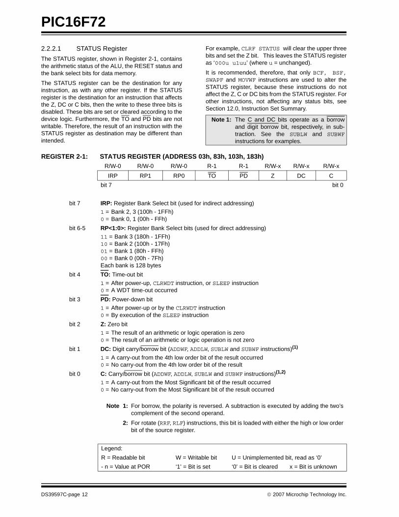
2.2.2.1 STATUS Register
The STATUS register, shown in Register 2-1, containsthe arithmetic status of the ALU, the RESET status andthe bank select bits for data memory.
The STATUS register can be the destination for anyinstruction, as with any other register. If the STATUSregister is the destination for an instruction that affectsthe Z, DC or C bits, then the write to these three bits isdisabled. These bits are set or cleared according to thedevice logic. Furthermore, the TO and PD bits are notwritable. Therefore, the result of an instruction with theSTATUS register as destination may be different thanintended.
For example, CLRF STATUS will clear the upper threebits and set the Z bit. This leaves the STATUS registeras ‘000u u1uu’ (where u = unchanged).
It is recommended, therefore, that only BCF, BSF,SWAPF and MOVWF instructions are used to alter theSTATUS register, because these instructions do notaffect the Z, C or DC bits from the STATUS register. Forother instructions, not affecting any status bits, seeSection 12.0, Instruction Set Summary.
REGISTER 2-1: STATUS REGISTER (ADDRESS 03h, 83h, 103h, 183h)
Note 1: The C and DC bits operate as a borrowand digit borrow bit, respectively, in sub-traction. See the SUBLW and SUBWFinstructions for examples.
R/W-0 R/W-0 R/W-0 R-1 R-1 R/W-x R/W-x R/W-x
IRP RP1 RP0 TO PD Z DC C
bit 7 bit 0
bit 7 IRP: Register Bank Select bit (used for indirect addressing)1 = Bank 2, 3 (100h - 1FFh) 0 = Bank 0, 1 (00h - FFh)
bit 6-5 RP<1:0>: Register Bank Select bits (used for direct addressing)11 = Bank 3 (180h - 1FFh)10 = Bank 2 (100h - 17Fh) 01 = Bank 1 (80h - FFh)00 = Bank 0 (00h - 7Fh)Each bank is 128 bytes
bit 4 TO: Time-out bit
1 = After power-up, CLRWDT instruction, or SLEEP instruction0 = A WDT time-out occurred
bit 3 PD: Power-down bit1 = After power-up or by the CLRWDT instruction0 = By execution of the SLEEP instruction
bit 2 Z: Zero bit1 = The result of an arithmetic or logic operation is zero0 = The result of an arithmetic or logic operation is not zero
bit 1 DC: Digit carry/borrow bit (ADDWF, ADDLW, SUBLW and SUBWF instructions)(1)
1 = A carry-out from the 4th low order bit of the result occurred0 = No carry-out from the 4th low order bit of the result
bit 0 C: Carry/borrow bit (ADDWF, ADDLW, SUBLW and SUBWF instructions)(1,2)
1 = A carry-out from the Most Significant bit of the result occurred0 = No carry-out from the Most Significant bit of the result occurred
Note 1: For borrow, the polarity is reversed. A subtraction is executed by adding the two’scomplement of the second operand.
2: For rotate (RRF, RLF) instructions, this bit is loaded with either the high or low orderbit of the source register.
Legend:
R = Readable bit W = Writable bit U = Unimplemented bit, read as ‘0’
- n = Value at POR ‘1’ = Bit is set ‘0’ = Bit is cleared x = Bit is unknown
DS39597C-page 12 © 2007 Microchip Technology Inc.
PIC16F72
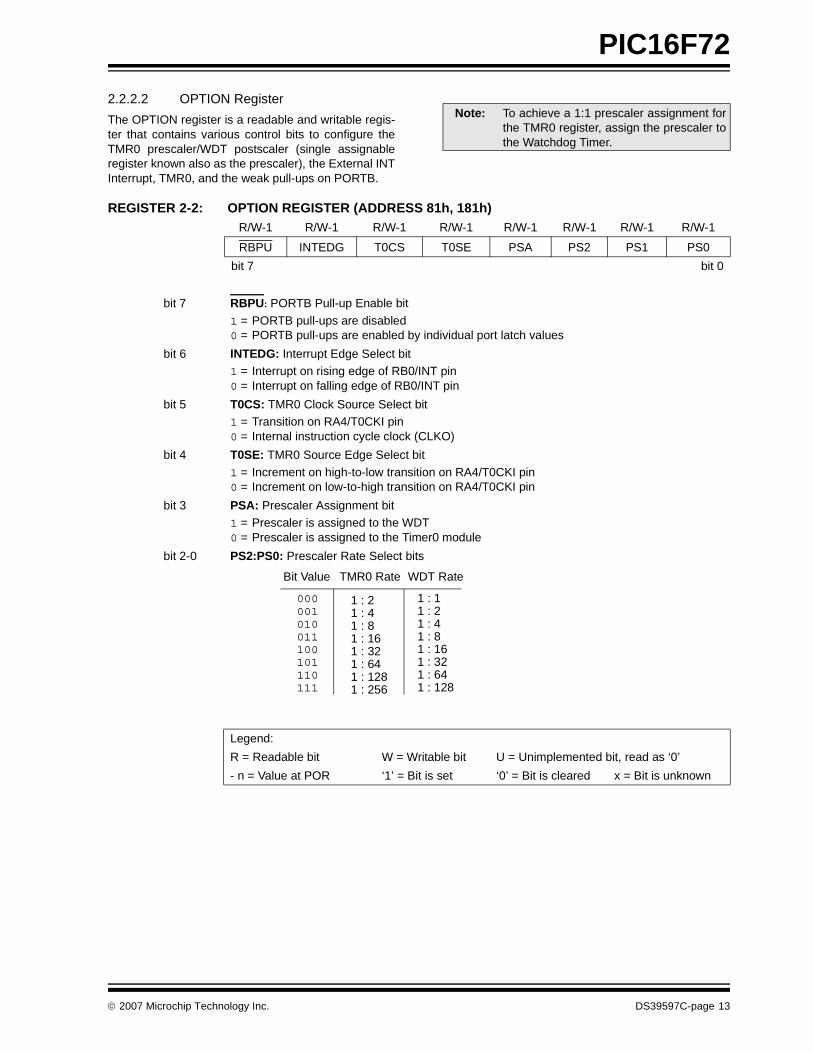
2.2.2.2 OPTION Register
The OPTION register is a readable and writable regis-ter that contains various control bits to configure theTMR0 prescaler/WDT postscaler (single assignableregister known also as the prescaler), the External INTInterrupt, TMR0, and the weak pull-ups on PORTB.
REGISTER 2-2: OPTION REGISTER (ADDRESS 81h, 181h)
Note: To achieve a 1:1 prescaler assignment forthe TMR0 register, assign the prescaler tothe Watchdog Timer.
R/W-1 R/W-1 R/W-1 R/W-1 R/W-1 R/W-1 R/W-1 R/W-1
RBPU INTEDG T0CS T0SE PSA PS2 PS1 PS0
bit 7 bit 0
bit 7 RBPU: PORTB Pull-up Enable bit
1 = PORTB pull-ups are disabled0 = PORTB pull-ups are enabled by individual port latch values
bit 6 INTEDG: Interrupt Edge Select bit1 = Interrupt on rising edge of RB0/INT pin0 = Interrupt on falling edge of RB0/INT pin
bit 5 T0CS: TMR0 Clock Source Select bit1 = Transition on RA4/T0CKI pin0 = Internal instruction cycle clock (CLKO)
bit 4 T0SE: TMR0 Source Edge Select bit
1 = Increment on high-to-low transition on RA4/T0CKI pin0 = Increment on low-to-high transition on RA4/T0CKI pin
bit 3 PSA: Prescaler Assignment bit1 = Prescaler is assigned to the WDT0 = Prescaler is assigned to the Timer0 module
bit 2-0 PS2:PS0: Prescaler Rate Select bits
Legend:
R = Readable bit W = Writable bit U = Unimplemented bit, read as ‘0’
- n = Value at POR ‘1’ = Bit is set ‘0’ = Bit is cleared x = Bit is unknown
000001010011100101110111
1 : 21 : 41 : 81 : 161 : 321 : 641 : 1281 : 256
1 : 11 : 21 : 41 : 81 : 161 : 321 : 641 : 128
Bit Value TMR0 Rate WDT Rate
© 2007 Microchip Technology Inc. DS39597C-page 13
PIC16F72
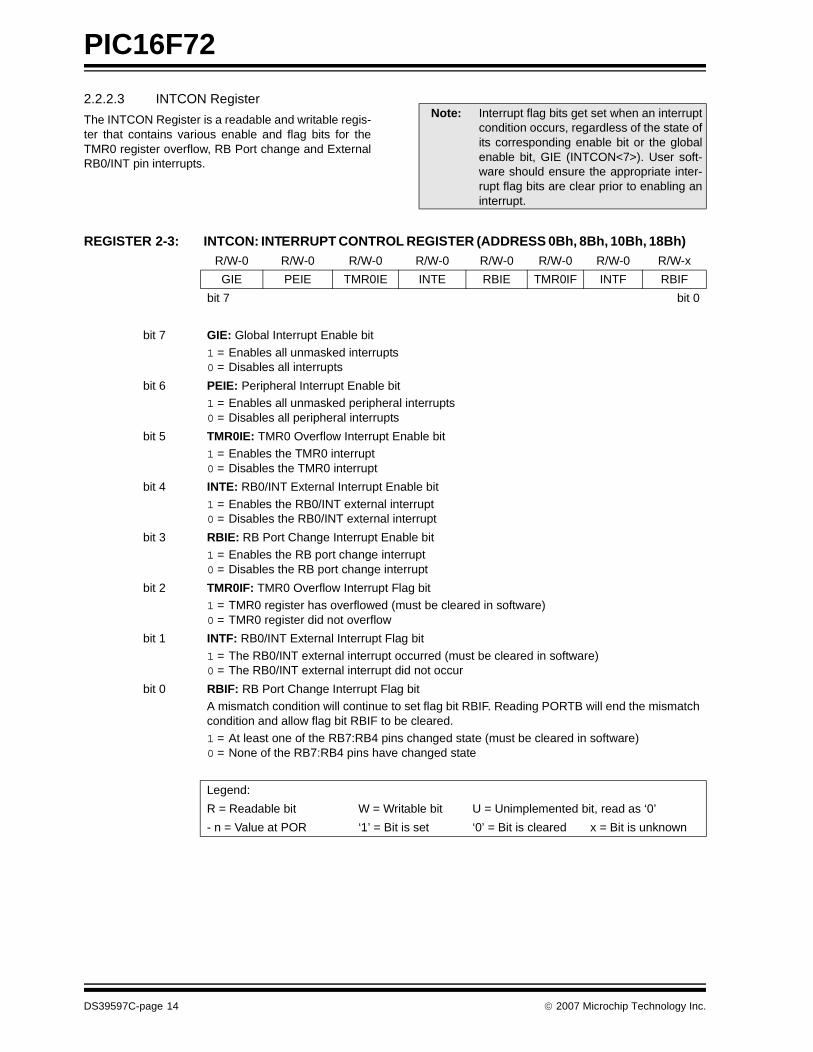
2.2.2.3 INTCON Register
The INTCON Register is a readable and writable regis-ter that contains various enable and flag bits for theTMR0 register overflow, RB Port change and ExternalRB0/INT pin interrupts.
REGISTER 2-3: INTCON: INTERRUPT CONTROL REGISTER (ADDRESS 0Bh, 8Bh, 10Bh, 18Bh)
Note: Interrupt flag bits get set when an interruptcondition occurs, regardless of the state ofits corresponding enable bit or the globalenable bit, GIE (INTCON<7>). User soft-ware should ensure the appropriate inter-rupt flag bits are clear prior to enabling aninterrupt.
R/W-0 R/W-0 R/W-0 R/W-0 R/W-0 R/W-0 R/W-0 R/W-x
GIE PEIE TMR0IE INTE RBIE TMR0IF INTF RBIF
bit 7 bit 0
bit 7 GIE: Global Interrupt Enable bit
1 = Enables all unmasked interrupts0 = Disables all interrupts
bit 6 PEIE: Peripheral Interrupt Enable bit1 = Enables all unmasked peripheral interrupts0 = Disables all peripheral interrupts
bit 5 TMR0IE: TMR0 Overflow Interrupt Enable bit1 = Enables the TMR0 interrupt0 = Disables the TMR0 interrupt
bit 4 INTE: RB0/INT External Interrupt Enable bit
1 = Enables the RB0/INT external interrupt0 = Disables the RB0/INT external interrupt
bit 3 RBIE: RB Port Change Interrupt Enable bit1 = Enables the RB port change interrupt0 = Disables the RB port change interrupt
bit 2 TMR0IF: TMR0 Overflow Interrupt Flag bit1 = TMR0 register has overflowed (must be cleared in software)0 = TMR0 register did not overflow
bit 1 INTF: RB0/INT External Interrupt Flag bit
1 = The RB0/INT external interrupt occurred (must be cleared in software)0 = The RB0/INT external interrupt did not occur
bit 0 RBIF: RB Port Change Interrupt Flag bitA mismatch condition will continue to set flag bit RBIF. Reading PORTB will end the mismatchcondition and allow flag bit RBIF to be cleared.1 = At least one of the RB7:RB4 pins changed state (must be cleared in software)0 = None of the RB7:RB4 pins have changed state
Legend:
R = Readable bit W = Writable bit U = Unimplemented bit, read as ‘0’
- n = Value at POR ‘1’ = Bit is set ‘0’ = Bit is cleared x = Bit is unknown
DS39597C-page 14 © 2007 Microchip Technology Inc.
PIC16F72
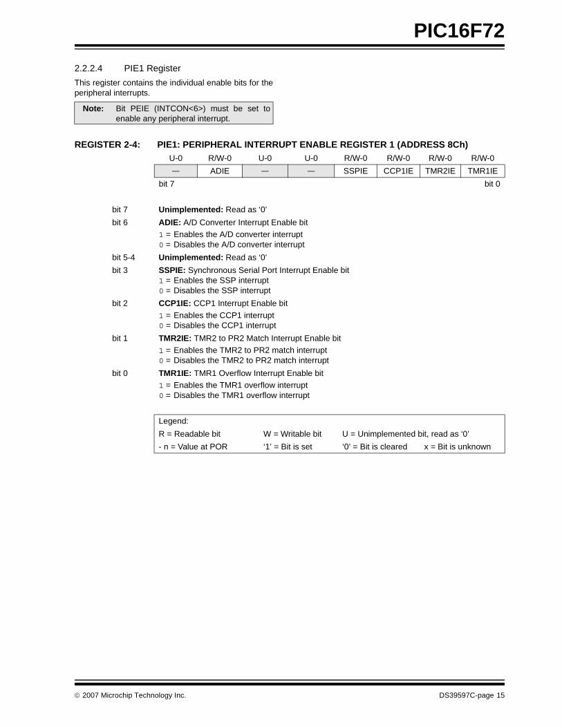
2.2.2.4 PIE1 Register
This register contains the individual enable bits for theperipheral interrupts.
REGISTER 2-4: PIE1: PERIPHERAL INTERRUPT ENABLE REGISTER 1 (ADDRESS 8Ch)
Note: Bit PEIE (INTCON<6>) must be set toenable any peripheral interrupt.
U-0 R/W-0 U-0 U-0 R/W-0 R/W-0 R/W-0 R/W-0
— ADIE — — SSPIE CCP1IE TMR2IE TMR1IE
bit 7 bit 0
bit 7 Unimplemented: Read as ‘0’
bit 6 ADIE: A/D Converter Interrupt Enable bit1 = Enables the A/D converter interrupt0 = Disables the A/D converter interrupt
bit 5-4 Unimplemented: Read as ‘0’
bit 3 SSPIE: Synchronous Serial Port Interrupt Enable bit1 = Enables the SSP interrupt0 = Disables the SSP interrupt
bit 2 CCP1IE: CCP1 Interrupt Enable bit
1 = Enables the CCP1 interrupt0 = Disables the CCP1 interrupt
bit 1 TMR2IE: TMR2 to PR2 Match Interrupt Enable bit1 = Enables the TMR2 to PR2 match interrupt0 = Disables the TMR2 to PR2 match interrupt
bit 0 TMR1IE: TMR1 Overflow Interrupt Enable bit1 = Enables the TMR1 overflow interrupt0 = Disables the TMR1 overflow interrupt
Legend:
R = Readable bit W = Writable bit U = Unimplemented bit, read as ‘0’
- n = Value at POR ‘1’ = Bit is set ‘0’ = Bit is cleared x = Bit is unknown
© 2007 Microchip Technology Inc. DS39597C-page 15
PIC16F72
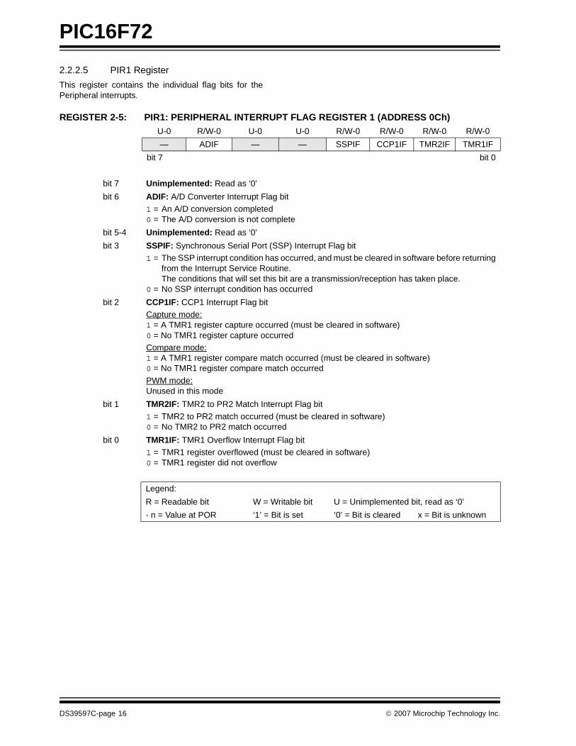
2.2.2.5 PIR1 Register
This register contains the individual flag bits for thePeripheral interrupts.
REGISTER 2-5: PIR1: PERIPHERAL INTERRUPT FLAG REGISTER 1 (ADDRESS 0Ch) U-0 R/W-0 U-0 U-0 R/W-0 R/W-0 R/W-0 R/W-0
— ADIF — — SSPIF CCP1IF TMR2IF TMR1IF
bit 7 bit 0
bit 7 Unimplemented: Read as ‘0’
bit 6 ADIF: A/D Converter Interrupt Flag bit1 = An A/D conversion completed0 = The A/D conversion is not complete
bit 5-4 Unimplemented: Read as ‘0’
bit 3 SSPIF: Synchronous Serial Port (SSP) Interrupt Flag bit1 = The SSP interrupt condition has occurred, and must be cleared in software before returning
from the Interrupt Service Routine. The conditions that will set this bit are a transmission/reception has taken place.
0 = No SSP interrupt condition has occurred
bit 2 CCP1IF: CCP1 Interrupt Flag bitCapture mode:1 = A TMR1 register capture occurred (must be cleared in software)0 = No TMR1 register capture occurredCompare mode:1 = A TMR1 register compare match occurred (must be cleared in software)0 = No TMR1 register compare match occurred
PWM mode:Unused in this mode
bit 1 TMR2IF: TMR2 to PR2 Match Interrupt Flag bit
1 = TMR2 to PR2 match occurred (must be cleared in software)0 = No TMR2 to PR2 match occurred
bit 0 TMR1IF: TMR1 Overflow Interrupt Flag bit1 = TMR1 register overflowed (must be cleared in software)0 = TMR1 register did not overflow
Legend:
R = Readable bit W = Writable bit U = Unimplemented bit, read as ‘0’
- n = Value at POR ‘1’ = Bit is set ‘0’ = Bit is cleared x = Bit is unknown
DS39597C-page 16 © 2007 Microchip Technology Inc.
PIC16F72
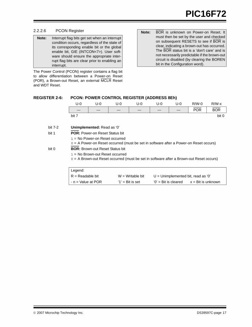
2.2.2.6 PCON Register
The Power Control (PCON) register contains a flag bitto allow differentiation between a Power-on Reset(POR), a Brown-out Reset, an external MCLR Resetand WDT Reset.
REGISTER 2-6: PCON: POWER CONTROL REGISTER (ADDRESS 8Eh)
Note: Interrupt flag bits get set when an interruptcondition occurs, regardless of the state ofits corresponding enable bit or the globalenable bit, GIE (INTCON<7>). User soft-ware should ensure the appropriate inter-rupt flag bits are clear prior to enabling aninterrupt.
Note: BOR is unknown on Power-on Reset. Itmust then be set by the user and checkedon subsequent RESETS to see if BOR isclear, indicating a brown-out has occurred.The BOR status bit is a ‘don't care’ and isnot necessarily predictable if the brown-outcircuit is disabled (by clearing the BORENbit in the Configuration word).
U-0 U-0 U-0 U-0 U-0 U-0 R/W-0 R/W-x
— — — — — — POR BOR
bit 7 bit 0
bit 7-2 Unimplemented: Read as ‘0’
bit 1 POR: Power-on Reset Status bit1 = No Power-on Reset occurred0 = A Power-on Reset occurred (must be set in software after a Power-on Reset occurs)
bit 0 BOR: Brown-out Reset Status bit
1 = No Brown-out Reset occurred0 = A Brown-out Reset occurred (must be set in software after a Brown-out Reset occurs)
Legend:
R = Readable bit W = Writable bit U = Unimplemented bit, read as ‘0’
- n = Value at POR ‘1’ = Bit is set ‘0’ = Bit is cleared x = Bit is unknown
© 2007 Microchip Technology Inc. DS39597C-page 17
PIC16F72
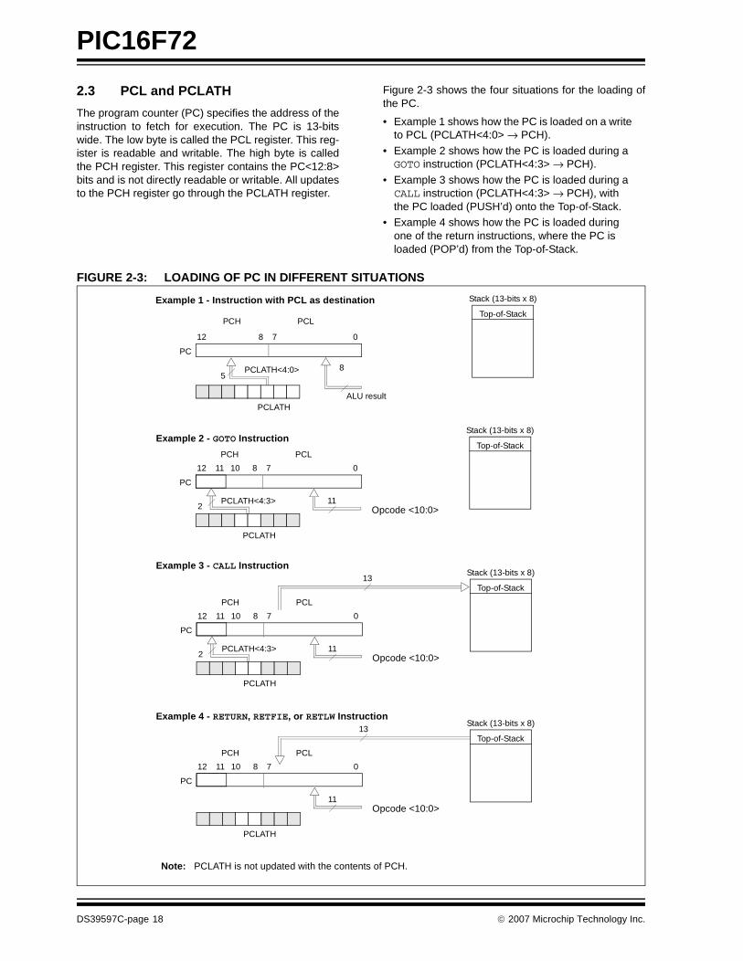
2.3 PCL and PCLATH
The program counter (PC) specifies the address of theinstruction to fetch for execution. The PC is 13-bitswide. The low byte is called the PCL register. This reg-ister is readable and writable. The high byte is calledthe PCH register. This register contains the PC<12:8>bits and is not directly readable or writable. All updatesto the PCH register go through the PCLATH register.
Figure 2-3 shows the four situations for the loading ofthe PC.
• Example 1 shows how the PC is loaded on a write to PCL (PCLATH<4:0> → PCH).
• Example 2 shows how the PC is loaded during a GOTO instruction (PCLATH<4:3> → PCH).
• Example 3 shows how the PC is loaded during a CALL instruction (PCLATH<4:3> → PCH), with the PC loaded (PUSH’d) onto the Top-of-Stack.
• Example 4 shows how the PC is loaded during one of the return instructions, where the PC is loaded (POP’d) from the Top-of-Stack.
FIGURE 2-3: LOADING OF PC IN DIFFERENT SITUATIONS
PC
12 8 7 0
5PCLATH<4:0>
PCLATHALU result
Opcode <10:0>
8
PC
12 11 10 0
11PCLATH<4:3>
PCH PCL
8 7
2
PCLATH
PCH PCL
Example 1 - Instruction with PCL as destination
Example 2 - GOTO Instruction
Stack (13-bits x 8)
Top-of-Stack
Stack (13-bits x 8)
Top-of-Stack
Opcode <10:0>
PC
12 11 10 0
11PCLATH<4:3>
8 7
2
PCLATH
PCH PCL
Example 3 - CALL InstructionStack (13-bits x 8)
Top-of-Stack
Opcode <10:0>
PC
12 11 10 0
11
8 7
PCLATH
PCH PCL
Example 4 - RETURN, RETFIE, or RETLW InstructionStack (13-bits x 8)
Top-of-Stack13
13
Note: PCLATH is not updated with the contents of PCH.
DS39597C-page 18 © 2007 Microchip Technology Inc.
PIC16F72
2.3.1 COMPUTED GOTO
A computed GOTO is accomplished by adding an offsetto the program counter (ADDWF PCL). When doing atable read using a computed GOTO method, careshould be exercised if the table location crosses a PCLmemory boundary (each 256-byte block). Refer to theApplication Note, “Implementing a Table Read"(AN556).
2.3.2 STACK
The stack allows a combination of up to eight programcalls and interrupts to occur. The stack contains thereturn address from this branch in program execution.
Mid-range devices have an 8-level deep x 13-bit widehardware stack. The stack space is not part of eitherprogram or data space and the stack pointer is notreadable or writable. The PC is PUSH’d onto the stackwhen a CALL instruction is executed, or an interruptcauses a branch. The stack is POP’d in the event of aRETURN, RETLW or a RETFIE instruction execution.PCLATH is not modified when the stack is PUSH’d orPOP’d.
After the stack has been PUSH’d eight times, the ninthpush overwrites the value that was stored from the firstpush. The tenth push overwrites the second push (andso on). An example of the overwriting of the stack isshown in Figure 2-4.
FIGURE 2-4: STACK MODIFICATION
2.4 Program Memory Paging
The CALL and GOTO instructions provide 11 bits ofaddress to allow branching within any 2K programmemory page. When doing a CALL or GOTO instruction,the upper two bits of the address are provided byPCLATH<4:3>. When doing a CALL or GOTO instruc-tion, the user must ensure that the page select bits areprogrammed so that the desired program memorypage is addressed. If a return from a CALL instruction(or interrupt) is executed, the entire 13-bit PC is pushedonto the stack. Therefore, manipulation of thePCLATH<4:3> bits is not required for the returninstructions (which POPs the address from the stack).
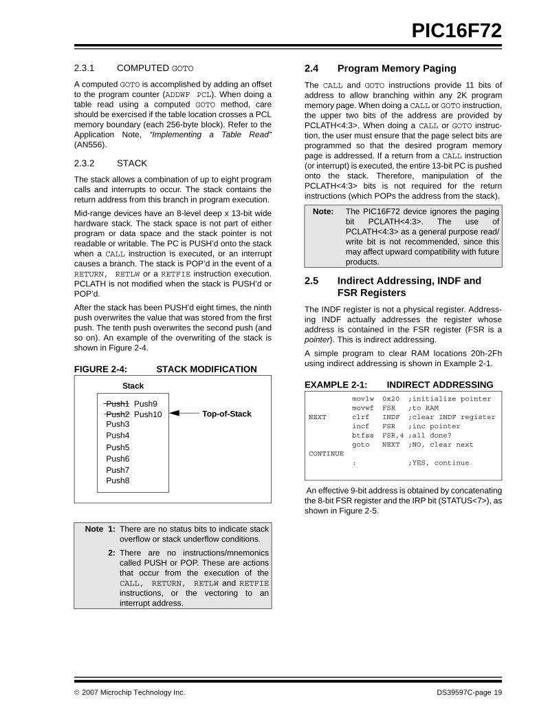
2.5 Indirect Addressing, INDF and FSR Registers
The INDF register is not a physical register. Address-ing INDF actually addresses the register whoseaddress is contained in the FSR register (FSR is apointer). This is indirect addressing.
A simple program to clear RAM locations 20h-2Fhusing indirect addressing is shown in Example 2-1.
EXAMPLE 2-1: INDIRECT ADDRESSING
An effective 9-bit address is obtained by concatenatingthe 8-bit FSR register and the IRP bit (STATUS<7>), asshown in Figure 2-5.
Note 1: There are no status bits to indicate stackoverflow or stack underflow conditions.
2: There are no instructions/mnemonicscalled PUSH or POP. These are actionsthat occur from the execution of theCALL, RETURN, RETLW and RETFIEinstructions, or the vectoring to aninterrupt address.
Push1 Push9Push2 Push10Push3Push4
Push5Push6Push7Push8
Top-of-Stack
Stack
Note: The PIC16F72 device ignores the pagingbit PCLATH<4:3>. The use ofPCLATH<4:3> as a general purpose read/write bit is not recommended, since thismay affect upward compatibility with futureproducts.
movlw 0x20 ;initialize pointer movwf FSR ;to RAMNEXT clrf INDF ;clear INDF register incf FSR ;inc pointer btfss FSR,4 ;all done? goto NEXT ;NO, clear nextCONTINUE : ;YES, continue
© 2007 Microchip Technology Inc. DS39597C-page 19
PIC16F72
FIGURE 2-5: DIRECT/INDIRECT ADDRESSING
Note 1: For register file map detail, see Figure 2-2.
DataMemory(1)
Indirect AddressingDirect Addressing
Bank Select Location Select
RP1:RP0 6 0From Opcode IRP FSR Register7 0
Bank Select Location Select
00 01 10 11
Bank 0 Bank 1 Bank 2 Bank 3
FFh
80h
7Fh
00h
17Fh
100h
1FFh
180h
DS39597C-page 20 © 2007 Microchip Technology Inc.
PIC16F72
3.0 I/O PORTS
Some pins for these I/O ports are multiplexed with analternate function for the peripheral features on thedevice. In general, when a peripheral is enabled, thatpin may not be used as a general purpose I/O pin.
Additional information on I/O ports may be found in thePIC™ Mid-Range MCU Reference Manual,(DS33023).
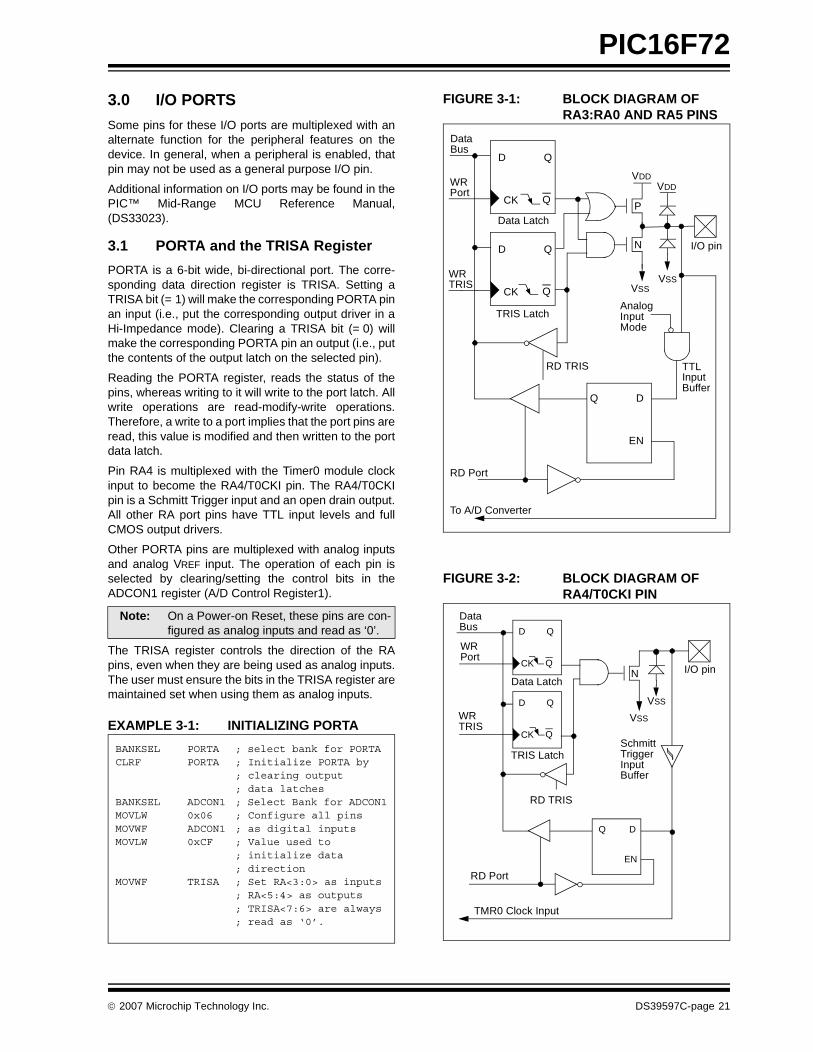
3.1 PORTA and the TRISA Register
PORTA is a 6-bit wide, bi-directional port. The corre-sponding data direction register is TRISA. Setting aTRISA bit (= 1) will make the corresponding PORTA pinan input (i.e., put the corresponding output driver in aHi-Impedance mode). Clearing a TRISA bit (= 0) willmake the corresponding PORTA pin an output (i.e., putthe contents of the output latch on the selected pin).
Reading the PORTA register, reads the status of thepins, whereas writing to it will write to the port latch. Allwrite operations are read-modify-write operations.Therefore, a write to a port implies that the port pins areread, this value is modified and then written to the portdata latch.
Pin RA4 is multiplexed with the Timer0 module clockinput to become the RA4/T0CKI pin. The RA4/T0CKIpin is a Schmitt Trigger input and an open drain output.All other RA port pins have TTL input levels and fullCMOS output drivers.
Other PORTA pins are multiplexed with analog inputsand analog VREF input. The operation of each pin isselected by clearing/setting the control bits in theADCON1 register (A/D Control Register1).
The TRISA register controls the direction of the RApins, even when they are being used as analog inputs.The user must ensure the bits in the TRISA register aremaintained set when using them as analog inputs.
EXAMPLE 3-1: INITIALIZING PORTA
FIGURE 3-1: BLOCK DIAGRAM OF RA3:RA0 AND RA5 PINS
FIGURE 3-2: BLOCK DIAGRAM OF RA4/T0CKI PIN
Note: On a Power-on Reset, these pins are con-figured as analog inputs and read as ‘0’.
BANKSEL PORTA ; select bank for PORTA CLRF PORTA ; Initialize PORTA by ; clearing output ; data latchesBANKSEL ADCON1 ; Select Bank for ADCON1MOVLW 0x06 ; Configure all pinsMOVWF ADCON1 ; as digital inputsMOVLW 0xCF ; Value used to ; initialize data ; directionMOVWF TRISA ; Set RA<3:0> as inputs ; RA<5:4> as outputs ; TRISA<7:6> are always ; read as ‘0’.
DataBus
QD
QCK
QD
QCK
Q D
EN
P
N
WRPort
WRTRIS
Data Latch
TRIS Latch
RD TRIS
RD Port
VSS
VDD
I/O pin
AnalogInputMode
TTLInputBuffer
To A/D Converter
VDD
VSS
DataBus
WRPort
WRTRIS
RD Port
Data Latch
TRIS Latch
RD TRIS
SchmittTriggerInputBuffer
N
VSS
I/O pin
TMR0 Clock Input
QD
QCK
QD
QCK
EN
Q D
EN
VSS
© 2007 Microchip Technology Inc. DS39597C-page 21
PIC16F72
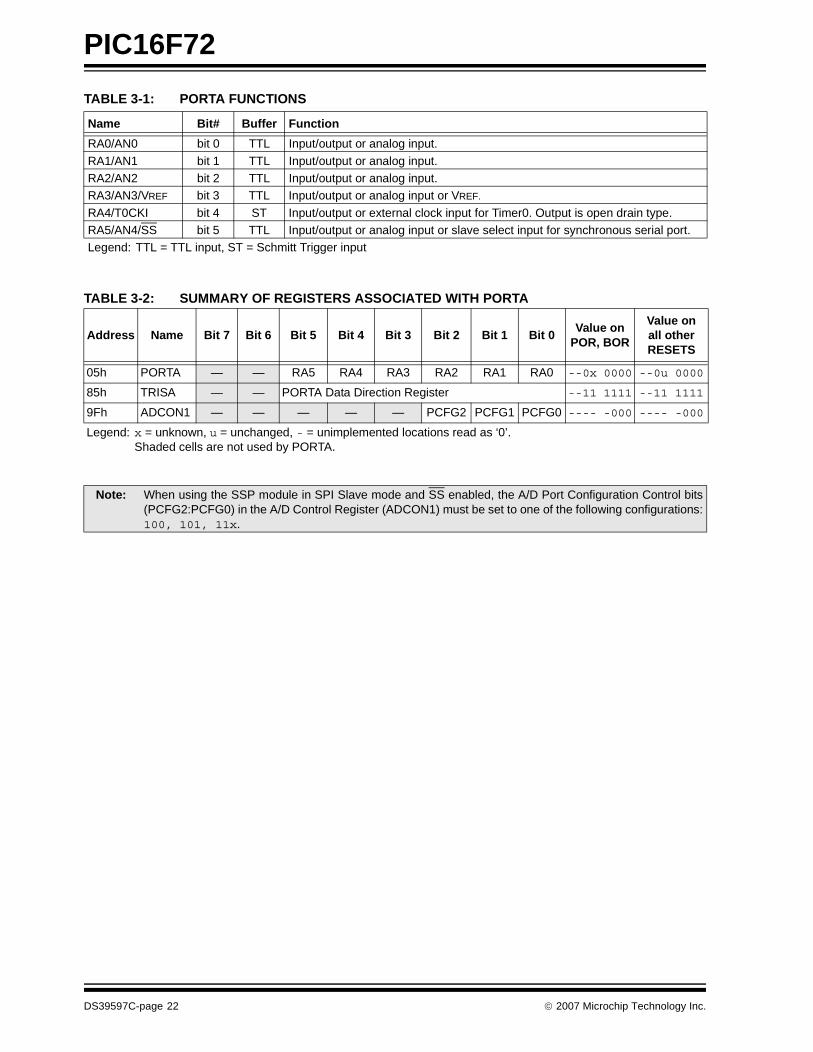
TABLE 3-1: PORTA FUNCTIONS
TABLE 3-2: SUMMARY OF REGISTERS ASSOCIATED WITH PORTA
Name Bit# Buffer Function
RA0/AN0 bit 0 TTL Input/output or analog input.
RA1/AN1 bit 1 TTL Input/output or analog input.RA2/AN2 bit 2 TTL Input/output or analog input.RA3/AN3/VREF bit 3 TTL Input/output or analog input or VREF.
RA4/T0CKI bit 4 ST Input/output or external clock input for Timer0. Output is open drain type.RA5/AN4/SS bit 5 TTL Input/output or analog input or slave select input for synchronous serial port.Legend: TTL = TTL input, ST = Schmitt Trigger input
Address Name Bit 7 Bit 6 Bit 5 Bit 4 Bit 3 Bit 2 Bit 1 Bit 0Value on
POR, BOR
Value on all other RESETS
05h PORTA — — RA5 RA4 RA3 RA2 RA1 RA0 --0x 0000 --0u 0000
85h TRISA — — PORTA Data Direction Register --11 1111 --11 1111
9Fh ADCON1 — — — — — PCFG2 PCFG1 PCFG0 ---- -000 ---- -000
Legend: x = unknown, u = unchanged, - = unimplemented locations read as ‘0’. Shaded cells are not used by PORTA.
Note: When using the SSP module in SPI Slave mode and SS enabled, the A/D Port Configuration Control bits(PCFG2:PCFG0) in the A/D Control Register (ADCON1) must be set to one of the following configurations:100, 101, 11x.
DS39597C-page 22 © 2007 Microchip Technology Inc.
PIC16F72
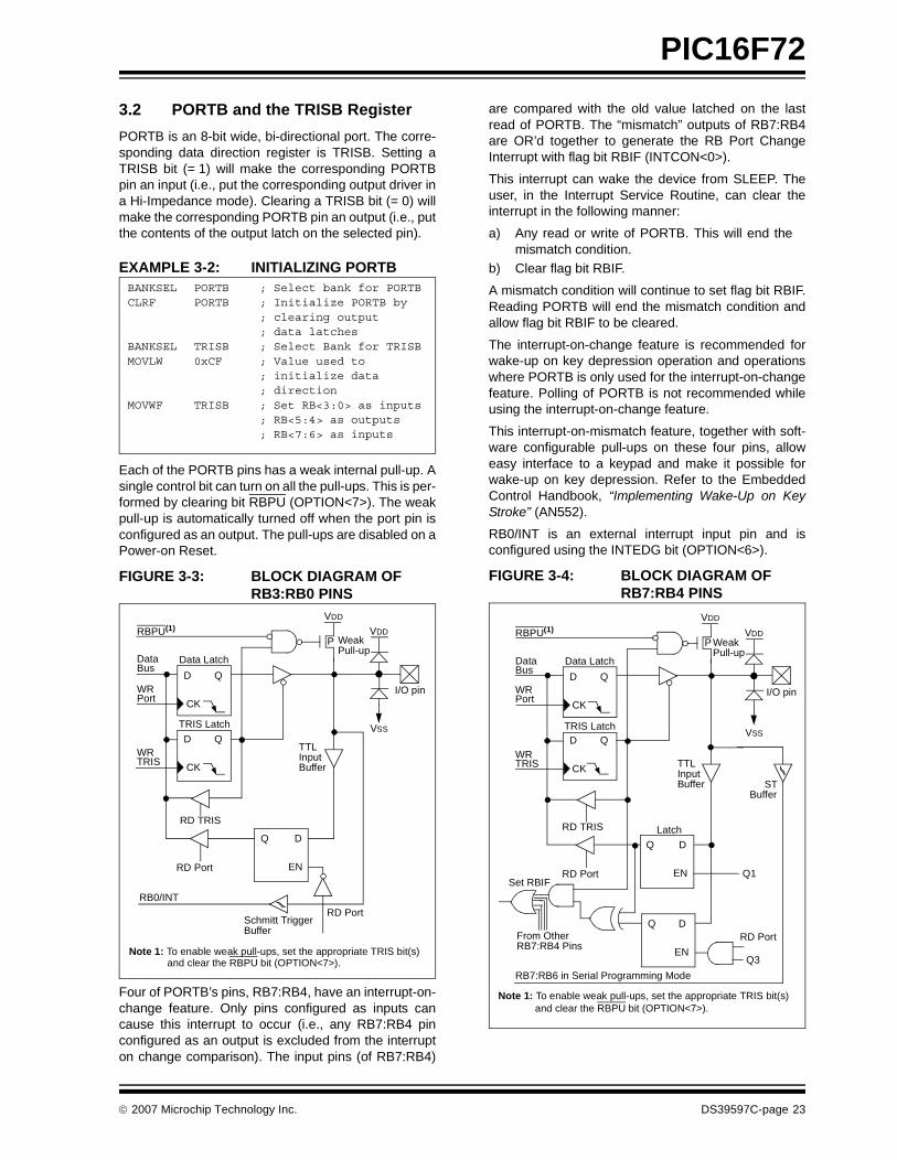
3.2 PORTB and the TRISB Register
PORTB is an 8-bit wide, bi-directional port. The corre-sponding data direction register is TRISB. Setting aTRISB bit (= 1) will make the corresponding PORTBpin an input (i.e., put the corresponding output driver ina Hi-Impedance mode). Clearing a TRISB bit (= 0) willmake the corresponding PORTB pin an output (i.e., putthe contents of the output latch on the selected pin).
EXAMPLE 3-2: INITIALIZING PORTB
Each of the PORTB pins has a weak internal pull-up. Asingle control bit can turn on all the pull-ups. This is per-formed by clearing bit RBPU (OPTION<7>). The weakpull-up is automatically turned off when the port pin isconfigured as an output. The pull-ups are disabled on aPower-on Reset.
FIGURE 3-3: BLOCK DIAGRAM OF RB3:RB0 PINS
Four of PORTB’s pins, RB7:RB4, have an interrupt-on-change feature. Only pins configured as inputs cancause this interrupt to occur (i.e., any RB7:RB4 pinconfigured as an output is excluded from the interrupton change comparison). The input pins (of RB7:RB4)
are compared with the old value latched on the lastread of PORTB. The “mismatch” outputs of RB7:RB4are OR’d together to generate the RB Port ChangeInterrupt with flag bit RBIF (INTCON<0>).
This interrupt can wake the device from SLEEP. Theuser, in the Interrupt Service Routine, can clear theinterrupt in the following manner:
a) Any read or write of PORTB. This will end themismatch condition.
b) Clear flag bit RBIF.
A mismatch condition will continue to set flag bit RBIF.Reading PORTB will end the mismatch condition andallow flag bit RBIF to be cleared.
The interrupt-on-change feature is recommended forwake-up on key depression operation and operationswhere PORTB is only used for the interrupt-on-changefeature. Polling of PORTB is not recommended whileusing the interrupt-on-change feature.
This interrupt-on-mismatch feature, together with soft-ware configurable pull-ups on these four pins, alloweasy interface to a keypad and make it possible forwake-up on key depression. Refer to the EmbeddedControl Handbook, “Implementing Wake-Up on KeyStroke” (AN552).
RB0/INT is an external interrupt input pin and isconfigured using the INTEDG bit (OPTION<6>).
FIGURE 3-4: BLOCK DIAGRAM OFRB7:RB4 PINS
BANKSEL PORTB ; Select bank for PORTBCLRF PORTB ; Initialize PORTB by ; clearing output ; data latchesBANKSEL TRISB ; Select Bank for TRISBMOVLW 0xCF ; Value used to ; initialize data ; directionMOVWF TRISB ; Set RB<3:0> as inputs ; RB<5:4> as outputs ; RB<7:6> as inputs
Data Latch
RBPU(1)
P
VDD
QD
CK
QD
CK
Q D
EN
Data
WR
WR
RD TRIS
RD Port
WeakPull-up
RD Port
RB0/INT
I/O pin
TTLInputBuffer
Note 1: To enable weak pull-ups, set the appropriate TRIS bit(s)
Schmitt TriggerBuffer
TRIS Latch
VDD
VSS
and clear the RBPU bit (OPTION<7>).
Bus
Port
TRIS
Data Latch
From Other
RBPU(1)
P
VDD
I/O pin
QD
CK
QD
CK
Q D
EN
Q D
EN
Data
WR
WR
Set RBIF
TRIS Latch
RD TRIS
RD Port
RB7:RB4 Pins
WeakPull-up
RD Port
Latch
TTLInputBuffer
Note 1: To enable weak pull-ups, set the appropriate TRIS bit(s)
STBuffer
RB7:RB6 in Serial Programming Mode
Q3
Q1
VDD
VSS
and clear the RBPU bit (OPTION<7>).
Bus
Port
TRIS
© 2007 Microchip Technology Inc. DS39597C-page 23
PIC16F72
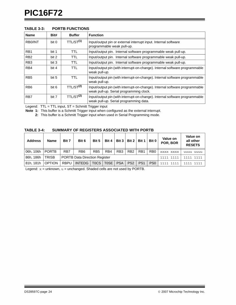
TABLE 3-3: PORTB FUNCTIONS
TABLE 3-4: SUMMARY OF REGISTERS ASSOCIATED WITH PORTB
Name Bit# Buffer Function
RB0/INT bit 0 TTL/ST(1) Input/output pin or external interrupt input. Internal software programmable weak pull-up.
RB1 bit 1 TTL Input/output pin. Internal software programmable weak pull-up.
RB2 bit 2 TTL Input/output pin. Internal software programmable weak pull-up.
RB3 bit 3 TTL Input/output pin. Internal software programmable weak pull-up.
RB4 bit 4 TTL Input/output pin (with interrupt-on-change). Internal software programmable weak pull-up.
RB5 bit 5 TTL Input/output pin (with interrupt-on-change). Internal software programmable weak pull-up.
RB6 bit 6 TTL/ST(2) Input/output pin (with interrupt-on-change). Internal software programmable weak pull-up. Serial programming clock.
RB7 bit 7 TTL/ST(2) Input/output pin (with interrupt-on-change). Internal software programmable weak pull-up. Serial programming data.
Legend: TTL = TTL input, ST = Schmitt Trigger inputNote 1: This buffer is a Schmitt Trigger input when configured as the external interrupt.
2: This buffer is a Schmitt Trigger input when used in Serial Programming mode.
Address Name Bit 7 Bit 6 Bit 5 Bit 4 Bit 3 Bit 2 Bit 1 Bit 0Value on
POR, BOR
Value on all other RESETS
06h, 106h PORTB RB7 RB6 RB5 RB4 RB3 RB2 RB1 RB0 xxxx xxxx uuuu uuuu
86h, 186h TRISB PORTB Data Direction Register 1111 1111 1111 1111
81h, 181h OPTION RBPU INTEDG T0CS T0SE PSA PS2 PS1 PS0 1111 1111 1111 1111
Legend: x = unknown, u = unchanged. Shaded cells are not used by PORTB.
DS39597C-page 24 © 2007 Microchip Technology Inc.
PIC16F72
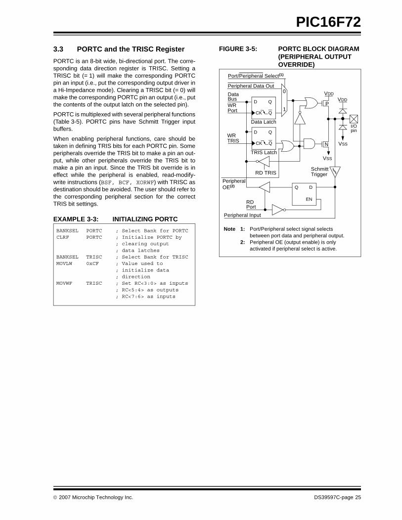
3.3 PORTC and the TRISC Register
PORTC is an 8-bit wide, bi-directional port. The corre-sponding data direction register is TRISC. Setting aTRISC bit (= 1) will make the corresponding PORTCpin an input (i.e., put the corresponding output driver ina Hi-Impedance mode). Clearing a TRISC bit (= 0) willmake the corresponding PORTC pin an output (i.e., putthe contents of the output latch on the selected pin).
PORTC is multiplexed with several peripheral functions(Table 3-5). PORTC pins have Schmitt Trigger inputbuffers.
When enabling peripheral functions, care should betaken in defining TRIS bits for each PORTC pin. Someperipherals override the TRIS bit to make a pin an out-put, while other peripherals override the TRIS bit tomake a pin an input. Since the TRIS bit override is ineffect while the peripheral is enabled, read-modify-write instructions (BSF, BCF, XORWF) with TRISC asdestination should be avoided. The user should refer tothe corresponding peripheral section for the correctTRIS bit settings.
EXAMPLE 3-3: INITIALIZING PORTC
FIGURE 3-5: PORTC BLOCK DIAGRAM (PERIPHERAL OUTPUT OVERRIDE)
BANKSEL PORTC ; Select Bank for PORTCCLRF PORTC ; Initialize PORTC by ; clearing output ; data latchesBANKSEL TRISC ; Select Bank for TRISCMOVLW 0xCF ; Value used to ; initialize data ; directionMOVWF TRISC ; Set RC<3:0> as inputs ; RC<5:4> as outputs ; RC<7:6> as inputs
Port/Peripheral Select(1)
Data
WRPort
WRTRIS
RD
Data Latch
TRIS Latch
RD TRISSchmittTrigger
QD
QCK
Q D
EN
Peripheral Data Out0
1
QD
QCK
P
N
VDD
VSS
Port
PeripheralOE(2)
Peripheral Input
Note 1: Port/Peripheral select signal selects between port data and peripheral output.
2: Peripheral OE (output enable) is only activated if peripheral select is active.
VSS
I/Opin
VDDBus
© 2007 Microchip Technology Inc. DS39597C-page 25
PIC16F72
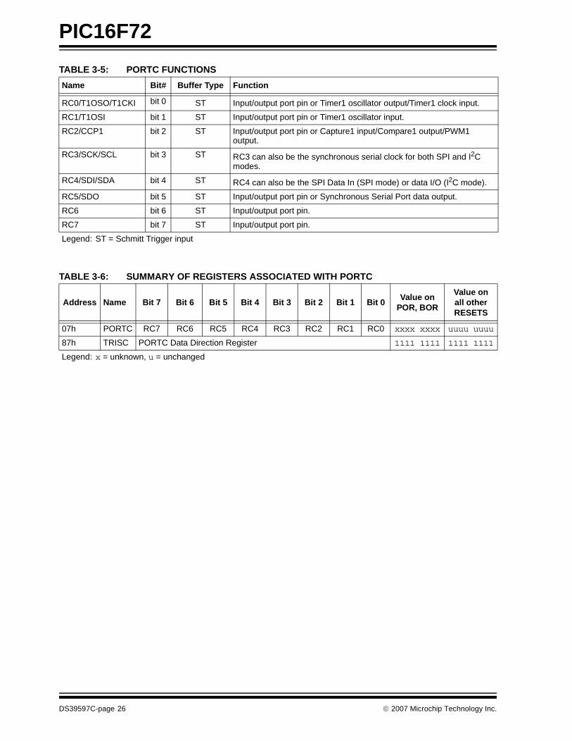
TABLE 3-5: PORTC FUNCTIONS
TABLE 3-6: SUMMARY OF REGISTERS ASSOCIATED WITH PORTC
Name Bit# Buffer Type Function
RC0/T1OSO/T1CKI bit 0 ST Input/output port pin or Timer1 oscillator output/Timer1 clock input.
RC1/T1OSI bit 1 ST Input/output port pin or Timer1 oscillator input.
RC2/CCP1 bit 2 ST Input/output port pin or Capture1 input/Compare1 output/PWM1 output.
RC3/SCK/SCL bit 3 ST RC3 can also be the synchronous serial clock for both SPI and I2C modes.
RC4/SDI/SDA bit 4 ST RC4 can also be the SPI Data In (SPI mode) or data I/O (I2C mode).
RC5/SDO bit 5 ST Input/output port pin or Synchronous Serial Port data output.
RC6 bit 6 ST Input/output port pin.
RC7 bit 7 ST Input/output port pin.
Legend: ST = Schmitt Trigger input
Address Name Bit 7 Bit 6 Bit 5 Bit 4 Bit 3 Bit 2 Bit 1 Bit 0Value on
POR, BOR
Value on all other RESETS
07h PORTC RC7 RC6 RC5 RC4 RC3 RC2 RC1 RC0 xxxx xxxx uuuu uuuu
87h TRISC PORTC Data Direction Register 1111 1111 1111 1111
Legend: x = unknown, u = unchanged
DS39597C-page 26 © 2007 Microchip Technology Inc.
PIC16F72
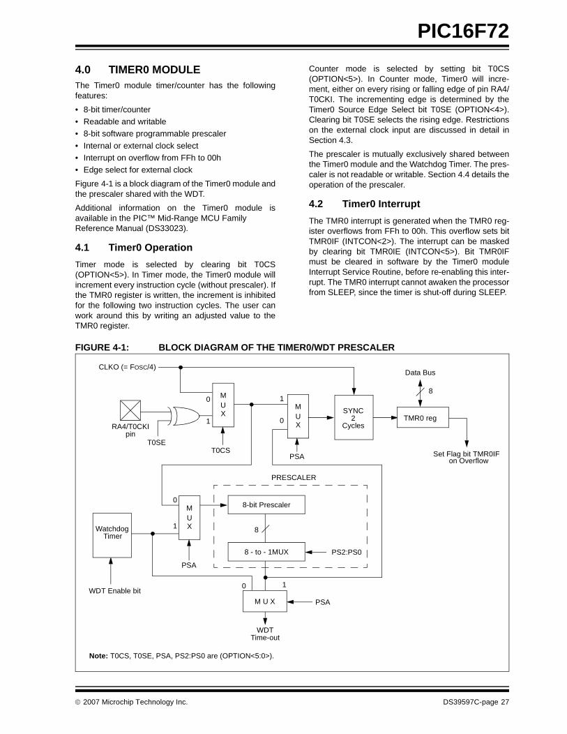
4.0 TIMER0 MODULEThe Timer0 module timer/counter has the followingfeatures:
• 8-bit timer/counter• Readable and writable• 8-bit software programmable prescaler
• Internal or external clock select• Interrupt on overflow from FFh to 00h• Edge select for external clock
Figure 4-1 is a block diagram of the Timer0 module andthe prescaler shared with the WDT.
Additional information on the Timer0 module isavailable in the PIC™ Mid-Range MCU Family Reference Manual (DS33023).
4.1 Timer0 Operation
Timer mode is selected by clearing bit T0CS(OPTION<5>). In Timer mode, the Timer0 module willincrement every instruction cycle (without prescaler). Ifthe TMR0 register is written, the increment is inhibitedfor the following two instruction cycles. The user canwork around this by writing an adjusted value to theTMR0 register.
Counter mode is selected by setting bit T0CS(OPTION<5>). In Counter mode, Timer0 will incre-ment, either on every rising or falling edge of pin RA4/T0CKI. The incrementing edge is determined by theTimer0 Source Edge Select bit T0SE (OPTION<4>).Clearing bit T0SE selects the rising edge. Restrictionson the external clock input are discussed in detail inSection 4.3.
The prescaler is mutually exclusively shared betweenthe Timer0 module and the Watchdog Timer. The pres-caler is not readable or writable. Section 4.4 details theoperation of the prescaler.
4.2 Timer0 Interrupt
The TMR0 interrupt is generated when the TMR0 reg-ister overflows from FFh to 00h. This overflow sets bitTMR0IF (INTCON<2>). The interrupt can be maskedby clearing bit TMR0IE (INTCON<5>). Bit TMR0IFmust be cleared in software by the Timer0 moduleInterrupt Service Routine, before re-enabling this inter-rupt. The TMR0 interrupt cannot awaken the processorfrom SLEEP, since the timer is shut-off during SLEEP.
FIGURE 4-1: BLOCK DIAGRAM OF THE TIMER0/WDT PRESCALER
RA4/T0CKI
T0SEpin
MUX
CLKO (= FOSC/4)
SYNC2
CyclesTMR0 reg
8-bit Prescaler
8 - to - 1MUX
MUX
M U X
WatchdogTimer
PSA
0 1
0
1
WDTTime-out
PS2:PS0
8
Note: T0CS, T0SE, PSA, PS2:PS0 are (OPTION<5:0>).
PSA
WDT Enable bit
MUX
0
1 0
1
Data Bus
Set Flag bit TMR0IFon Overflow
8
PSAT0CS
PRESCALER
© 2007 Microchip Technology Inc. DS39597C-page 27
PIC16F72
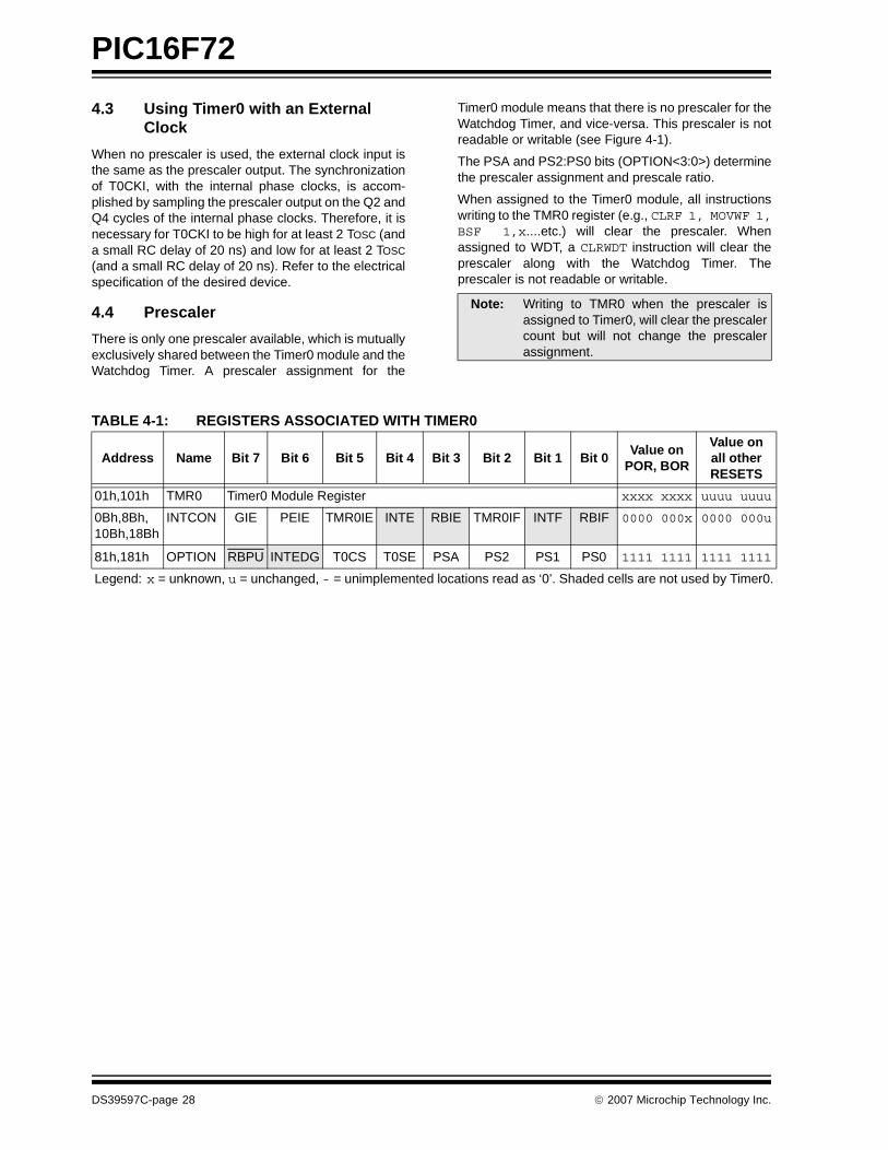
4.3 Using Timer0 with an External Clock
When no prescaler is used, the external clock input isthe same as the prescaler output. The synchronizationof T0CKI, with the internal phase clocks, is accom-plished by sampling the prescaler output on the Q2 andQ4 cycles of the internal phase clocks. Therefore, it isnecessary for T0CKI to be high for at least 2 TOSC (anda small RC delay of 20 ns) and low for at least 2 TOSC
(and a small RC delay of 20 ns). Refer to the electricalspecification of the desired device.
4.4 Prescaler
There is only one prescaler available, which is mutuallyexclusively shared between the Timer0 module and theWatchdog Timer. A prescaler assignment for the
Timer0 module means that there is no prescaler for theWatchdog Timer, and vice-versa. This prescaler is notreadable or writable (see Figure 4-1).
The PSA and PS2:PS0 bits (OPTION<3:0>) determinethe prescaler assignment and prescale ratio.
When assigned to the Timer0 module, all instructionswriting to the TMR0 register (e.g., CLRF 1, MOVWF 1,BSF 1,x....etc.) will clear the prescaler. Whenassigned to WDT, a CLRWDT instruction will clear theprescaler along with the Watchdog Timer. Theprescaler is not readable or writable.
TABLE 4-1: REGISTERS ASSOCIATED WITH TIMER0
Note: Writing to TMR0 when the prescaler isassigned to Timer0, will clear the prescalercount but will not change the prescalerassignment.
Address Name Bit 7 Bit 6 Bit 5 Bit 4 Bit 3 Bit 2 Bit 1 Bit 0Value on
POR, BOR
Value on all other RESETS
01h,101h TMR0 Timer0 Module Register xxxx xxxx uuuu uuuu
0Bh,8Bh,10Bh,18Bh
INTCON GIE PEIE TMR0IE INTE RBIE TMR0IF INTF RBIF 0000 000x 0000 000u
81h,181h OPTION RBPU INTEDG T0CS T0SE PSA PS2 PS1 PS0 1111 1111 1111 1111
Legend: x = unknown, u = unchanged, - = unimplemented locations read as ‘0’. Shaded cells are not used by Timer0.
DS39597C-page 28 © 2007 Microchip Technology Inc.
PIC16F72
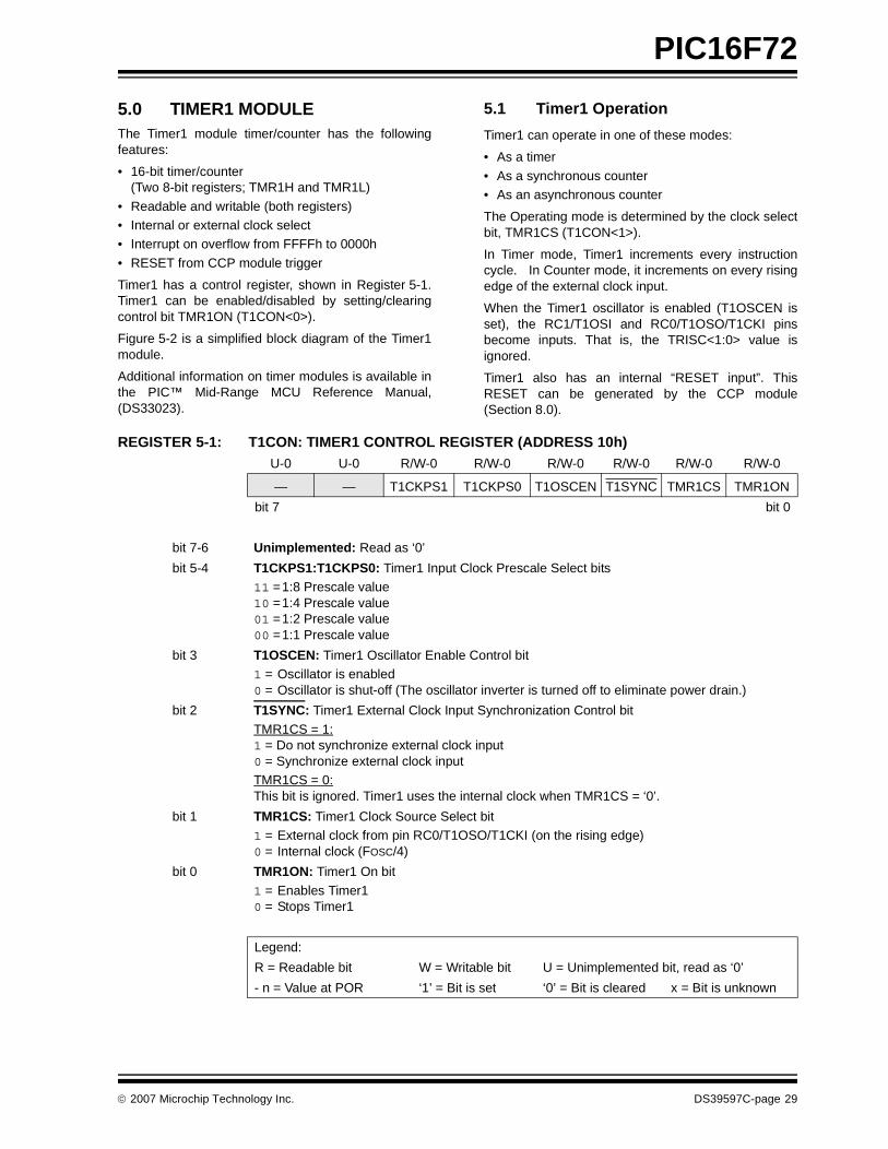
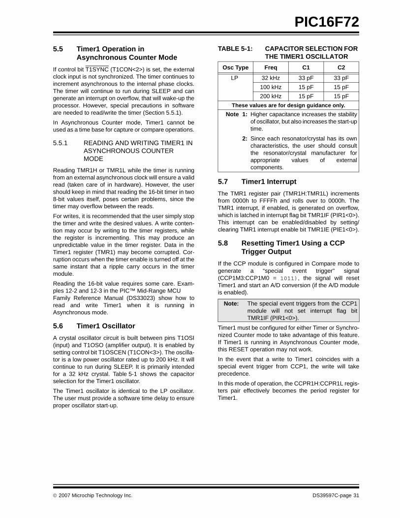
5.0 TIMER1 MODULEThe Timer1 module timer/counter has the followingfeatures:
• 16-bit timer/counter (Two 8-bit registers; TMR1H and TMR1L)
• Readable and writable (both registers)• Internal or external clock select• Interrupt on overflow from FFFFh to 0000h
• RESET from CCP module trigger
Timer1 has a control register, shown in Register 5-1.Timer1 can be enabled/disabled by setting/clearingcontrol bit TMR1ON (T1CON<0>).
Figure 5-2 is a simplified block diagram of the Timer1module.
Additional information on timer modules is available inthe PIC™ Mid-Range MCU Reference Manual,(DS33023).
5.1 Timer1 Operation
Timer1 can operate in one of these modes:
• As a timer
• As a synchronous counter• As an asynchronous counter
The Operating mode is determined by the clock selectbit, TMR1CS (T1CON<1>).
In Timer mode, Timer1 increments every instructioncycle. In Counter mode, it increments on every risingedge of the external clock input.
When the Timer1 oscillator is enabled (T1OSCEN isset), the RC1/T1OSI and RC0/T1OSO/T1CKI pinsbecome inputs. That is, the TRISC<1:0> value isignored.
Timer1 also has an internal “RESET input”. ThisRESET can be generated by the CCP module(Section 8.0).
REGISTER 5-1: T1CON: TIMER1 CONTROL REGISTER (ADDRESS 10h) U-0 U-0 R/W-0 R/W-0 R/W-0 R/W-0 R/W-0 R/W-0
— — T1CKPS1 T1CKPS0 T1OSCEN T1SYNC TMR1CS TMR1ON
bit 7 bit 0
bit 7-6 Unimplemented: Read as ‘0’
bit 5-4 T1CKPS1:T1CKPS0: Timer1 Input Clock Prescale Select bits11 =1:8 Prescale value10 =1:4 Prescale value01 =1:2 Prescale value00 =1:1 Prescale value
bit 3 T1OSCEN: Timer1 Oscillator Enable Control bit1 = Oscillator is enabled0 = Oscillator is shut-off (The oscillator inverter is turned off to eliminate power drain.)
bit 2 T1SYNC: Timer1 External Clock Input Synchronization Control bit
TMR1CS = 1:1 = Do not synchronize external clock input0 = Synchronize external clock inputTMR1CS = 0:This bit is ignored. Timer1 uses the internal clock when TMR1CS = ‘0’.
bit 1 TMR1CS: Timer1 Clock Source Select bit1 = External clock from pin RC0/T1OSO/T1CKI (on the rising edge)0 = Internal clock (FOSC/4)
bit 0 TMR1ON: Timer1 On bit
1 = Enables Timer10 = Stops Timer1
Legend:
R = Readable bit W = Writable bit U = Unimplemented bit, read as ‘0’
- n = Value at POR ‘1’ = Bit is set ‘0’ = Bit is cleared x = Bit is unknown
© 2007 Microchip Technology Inc. DS39597C-page 29
PIC16F72
5.2 Timer1 Operation in Timer Mode
Timer mode is selected by clearing the TMR1CS(T1CON<1>) bit. In this mode, the input clock to thetimer is FOSC/4. The synchronize control bit T1SYNC(T1CON<2>) has no effect, since the internal clock isalways in sync.
5.3 Timer1 Counter Operation
Timer1 may operate in Asynchronous or Synchronousmode, depending on the setting of the TMR1CS bit.
When Timer1 is being incremented via an externalsource, increments occur on a rising edge. After Timer1is enabled in Counter mode, the module must first havea falling edge before the counter begins to increment.
5.4 Timer1 Operation in Synchronized Counter Mode
Counter mode is selected by setting bit TMR1CS. Inthis mode, the timer increments on every rising edge ofclock input on pin RC1/T1OSI when bit T1OSCEN isset, or on pin RC0/T1OSO/T1CKI when bit T1OSCENis cleared.
If T1SYNC is cleared, then the external clock input issynchronized with internal phase clocks. The synchro-nization is done after the prescaler stage. Theprescaler stage is an asynchronous ripple counter.
In this configuration, during SLEEP mode, Timer1 willnot increment even if the external clock is present,since the synchronization circuit is shut-off. Theprescaler, however, will continue to increment.
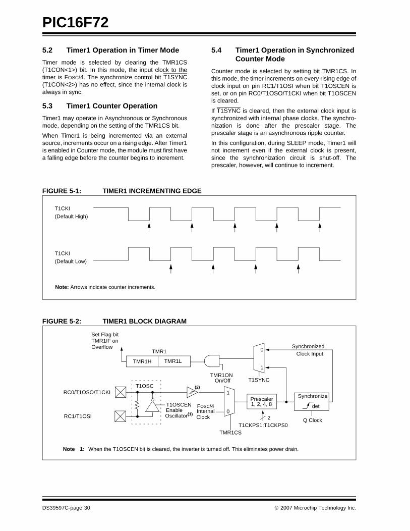
FIGURE 5-1: TIMER1 INCREMENTING EDGE
FIGURE 5-2: TIMER1 BLOCK DIAGRAM
T1CKI
(Default High)
T1CKI
(Default Low)
Note: Arrows indicate counter increments.
TMR1H TMR1L
T1OSCT1SYNC
TMR1CST1CKPS1:T1CKPS0
Q Clock
T1OSCENEnableOscillator(1)
FOSC/4InternalClock
TMR1ONOn/Off
Prescaler1, 2, 4, 8
Synchronize
det
1
0
0
1
SynchronizedClock Input
2
RC0/T1OSO/T1CKI
RC1/T1OSI
Note 1: When the T1OSCEN bit is cleared, the inverter is turned off. This eliminates power drain.
Set Flag bitTMR1IF onOverflow
TMR1
(2)
DS39597C-page 30 © 2007 Microchip Technology Inc.
PIC16F72
5.5 Timer1 Operation in Asynchronous Counter Mode
If control bit T1SYNC (T1CON<2>) is set, the externalclock input is not synchronized. The timer continues toincrement asynchronous to the internal phase clocks.The timer will continue to run during SLEEP and cangenerate an interrupt on overflow, that will wake-up theprocessor. However, special precautions in softwareare needed to read/write the timer (Section 5.5.1).
In Asynchronous Counter mode, Timer1 cannot beused as a time base for capture or compare operations.
5.5.1 READING AND WRITING TIMER1 IN ASYNCHRONOUS COUNTER MODE
Reading TMR1H or TMR1L while the timer is runningfrom an external asynchronous clock will ensure a validread (taken care of in hardware). However, the usershould keep in mind that reading the 16-bit timer in two8-bit values itself, poses certain problems, since thetimer may overflow between the reads.
For writes, it is recommended that the user simply stopthe timer and write the desired values. A write conten-tion may occur by writing to the timer registers, whilethe register is incrementing. This may produce anunpredictable value in the timer register. Data in theTimer1 register (TMR1) may become corrupted. Cor-ruption occurs when the timer enable is turned off at thesame instant that a ripple carry occurs in the timermodule.
Reading the 16-bit value requires some care. Exam-ples 12-2 and 12-3 in the PIC™ Mid-Range MCU Family Reference Manual (DS33023) show how toread and write Timer1 when it is running inAsynchronous mode.
5.6 Timer1 Oscillator
A crystal oscillator circuit is built between pins T1OSI(input) and T1OSO (amplifier output). It is enabled bysetting control bit T1OSCEN (T1CON<3>). The oscilla-tor is a low power oscillator rated up to 200 kHz. It willcontinue to run during SLEEP. It is primarily intendedfor a 32 kHz crystal. Table 5-1 shows the capacitorselection for the Timer1 oscillator.
The Timer1 oscillator is identical to the LP oscillator.The user must provide a software time delay to ensureproper oscillator start-up.
TABLE 5-1: CAPACITOR SELECTION FOR THE TIMER1 OSCILLATOR
5.7 Timer1 Interrupt
The TMR1 register pair (TMR1H:TMR1L) incrementsfrom 0000h to FFFFh and rolls over to 0000h. TheTMR1 interrupt, if enabled, is generated on overflow,which is latched in interrupt flag bit TMR1IF (PIR1<0>).This interrupt can be enabled/disabled by setting/clearing TMR1 interrupt enable bit TMR1IE (PIE1<0>).
5.8 Resetting Timer1 Using a CCP Trigger Output
If the CCP module is configured in Compare mode togenerate a “special event trigger" signal(CCP1M3:CCP1M0 = 1011), the signal will resetTimer1 and start an A/D conversion (if the A/D moduleis enabled).
Timer1 must be configured for either Timer or Synchro-nized Counter mode to take advantage of this feature.If Timer1 is running in Asynchronous Counter mode,this RESET operation may not work.
In the event that a write to Timer1 coincides with aspecial event trigger from CCP1, the write will takeprecedence.
In this mode of operation, the CCPR1H:CCPR1L regis-ters pair effectively becomes the period register forTimer1.
Osc Type Freq C1 C2
LP 32 kHz 33 pF 33 pF
100 kHz 15 pF 15 pF
200 kHz 15 pF 15 pF
These values are for design guidance only.
Note 1: Higher capacitance increases the stabilityof oscillator, but also increases the start-uptime.
2: Since each resonator/crystal has its owncharacteristics, the user should consultthe resonator/crystal manufacturer forappropriate values of externalcomponents.
Note: The special event triggers from the CCP1module will not set interrupt flag bitTMR1IF (PIR1<0>).
© 2007 Microchip Technology Inc. DS39597C-page 31
PIC16F72
5.9 Resetting Timer1 Register Pair (TMR1H, TMR1L)
TMR1H and TMR1L registers are not reset to 00h on aPOR, or any other RESET, except by the CCP1 specialevent triggers.
T1CON register is reset to 00h on a Power-on Reset ora Brown-out Reset, which shuts off the timer andleaves a 1:1 prescale. In all other RESETS, the registeris unaffected.
5.10 Timer1 Prescaler
The prescaler counter is cleared on writes to theTMR1H or TMR1L registers.
TABLE 5-2: REGISTERS ASSOCIATED WITH TIMER1 AS A TIMER/COUNTER
Address Name Bit 7 Bit 6 Bit 5 Bit 4 Bit 3 Bit 2 Bit 1 Bit 0Value on
POR, BOR
Value on all other RESETS
0Bh,8Bh,10Bh,18Bh
INTCON GIE PEIE TMR0IE INTE RBIE TMR0IF INTF RBIF 0000 000x 0000 000u
0Ch PIR1 — ADIF — — SSPIF CCP1IF TMR2IF TMR1IF 0000 0000 0000 0000
8Ch PIE1 — ADIE — — SSPIE CCP1IE TMR2IE TMR1IE 0000 0000 0000 0000
0Eh TMR1L Holding register for the Least Significant Byte of the 16-bit TMR1 Register xxxx xxxx uuuu uuuu
0Fh TMR1H Holding register for the Most Significant Byte of the 16-bit TMR1 Register xxxx xxxx uuuu uuuu
10h T1CON — — T1CKPS1 T1CKPS0 T1OSCEN T1SYNC TMR1CS TMR1ON --00 0000 --uu uuuu
Legend: x = unknown, u = unchanged, - = unimplemented, read as ‘0’. Shaded cells are not used by the Timer1 module.
DS39597C-page 32 © 2007 Microchip Technology Inc.

PIC16F72
6.0 TIMER2 MODULE
The Timer2 module timer has the following features:
• 8-bit timer (TMR2 register)• 8-bit period register (PR2)• Readable and writable (both registers)
• Software programmable prescaler (1:1, 1:4, 1:16)• Software programmable postscaler (1:1 to 1:16)• Interrupt on TMR2 match of PR2
• SSP module optional use of TMR2 output to generate clock shift
Timer2 has a control register, shown in Register 6-1.Timer2 can be shut-off by clearing control bit TMR2ON(T2CON<2>) to minimize power consumption.
Figure 6-1 is a simplified block diagram of the Timer2module.
Additional information on timer modules is available inthe PIC™ Mid-Range MCU Reference Manual,(DS33023).
6.1 Timer2 Operation
Timer2 can be used as the PWM time-base for PWMmode of the CCP module.
The TMR2 register is readable and writable, and iscleared on any device RESET.
The input clock (FOSC/4) has a prescale option of 1:1,1:4 or 1:16, selected by control bitsT2CKPS1:T2CKPS0 (T2CON<1:0>).
The match output of TMR2 goes through a 4-bitpostscaler (which gives a 1:1 to 1:16 scaling inclusive)to generate a TMR2 interrupt (latched in flag bitTMR2IF, (PIR1<1>)).
6.2 Timer2 Prescaler and Postscaler
The prescaler and postscaler counters are clearedwhen any of the following occurs:
• A write to the TMR2 register• A write to the T2CON register
• Any device RESET (Power-on Reset, MCLR , WDT Reset, or Brown-out Reset)
TMR2 is not cleared when T2CON is written.
6.3 Timer2 Interrupt
The Timer2 module has an 8-bit period register, PR2.Timer2 increments from 00h until it matches PR2 andthen resets to 00h on the next increment cycle. PR2 isa readable and writable register. The PR2 register isinitialized to FFh upon RESET.
6.4 Output of TMR2
The output of TMR2 (before the postscaler) is fed to theSynchronous Serial Port module, which optionally usesit to generate a shift clock.
FIGURE 6-1: TIMER2 BLOCK DIAGRAM
Comparator
TMR2Sets Flag
TMR2 reg
Output(1)
RESET
Postscaler
Prescaler
PR2 reg
2
FOSC/4
1:1 1:16
1:1, 1:4, 1:16
EQ
4
bit TMR2IF
Note 1: TMR2 register output can be software selected by the SSP module as a baud clock.
to
© 2007 Microchip Technology Inc. DS39597C-page 33
PIC16F72
REGISTER 6-1: T2CON: TIMER2 CONTROL REGISTER (ADDRESS 12h)
TABLE 6-1: REGISTERS ASSOCIATED WITH TIMER2 AS A TIMER/COUNTER
U-0 R/W-0 R/W-0 R/W-0 R/W-0 R/W-0 R/W-0 R/W-0
— TOUTPS3 TOUTPS2 TOUTPS1 TOUTPS0 TMR2ON T2CKPS1 T2CKPS0
bit 7 bit 0
bit 7 Unimplemented: Read as ‘0’
bit 6-3 TOUTPS3:TOUTPS0: Timer2 Output Postscale Select bits
0000 = 1:1 Postscale0001 = 1:2 Postscale0010 = 1:3 Postscale•••1111 = 1:16 Postscale
bit 2 TMR2ON: Timer2 On bit
1 = Timer2 is on0 = Timer2 is off
bit 1-0 T2CKPS1:T2CKPS0: Timer2 Clock Prescale Select bits00 = Prescaler is 101 = Prescaler is 41x = Prescaler is 16
Legend:
R = Readable bit W = Writable bit U = Unimplemented bit, read as ‘0’
- n = Value at POR ‘1’ = Bit is set ‘0’ = Bit is cleared x = Bit is unknown
Address Name Bit 7 Bit 6 Bit 5 Bit 4 Bit 3 Bit 2 Bit 1 Bit 0Value on
POR, BOR
Value on all other RESETS
0Bh,8Bh,10Bh, 18Bh
INTCON GIE PEIE TMR0IE INTE RBIE TMR0IF INTF RBIF 0000 000x 0000 000u
0Ch PIR1 — ADIF — — SSPIF CCP1IF TMR2IF TMR1IF -0-- 0000 0000 0000
8Ch PIE1 — ADIE — — SSPIE CCP1IE TMR2IE TMR1IE -0-- 0000 0000 0000
11h TMR2 Timer2 Module Register 0000 0000 0000 0000
12h T2CON — TOUTPS3 TOUTPS2 TOUTPS1 TOUTPS0 TMR2ON T2CKPS1 T2CKPS0 -000 0000 -000 0000
92h PR2 Timer2 Period Register 1111 1111 1111 1111
Legend: x = unknown, u = unchanged, - = unimplemented, read as ‘0’. Shaded cells are not used by the Timer2 module.
DS39597C-page 34 © 2007 Microchip Technology Inc.
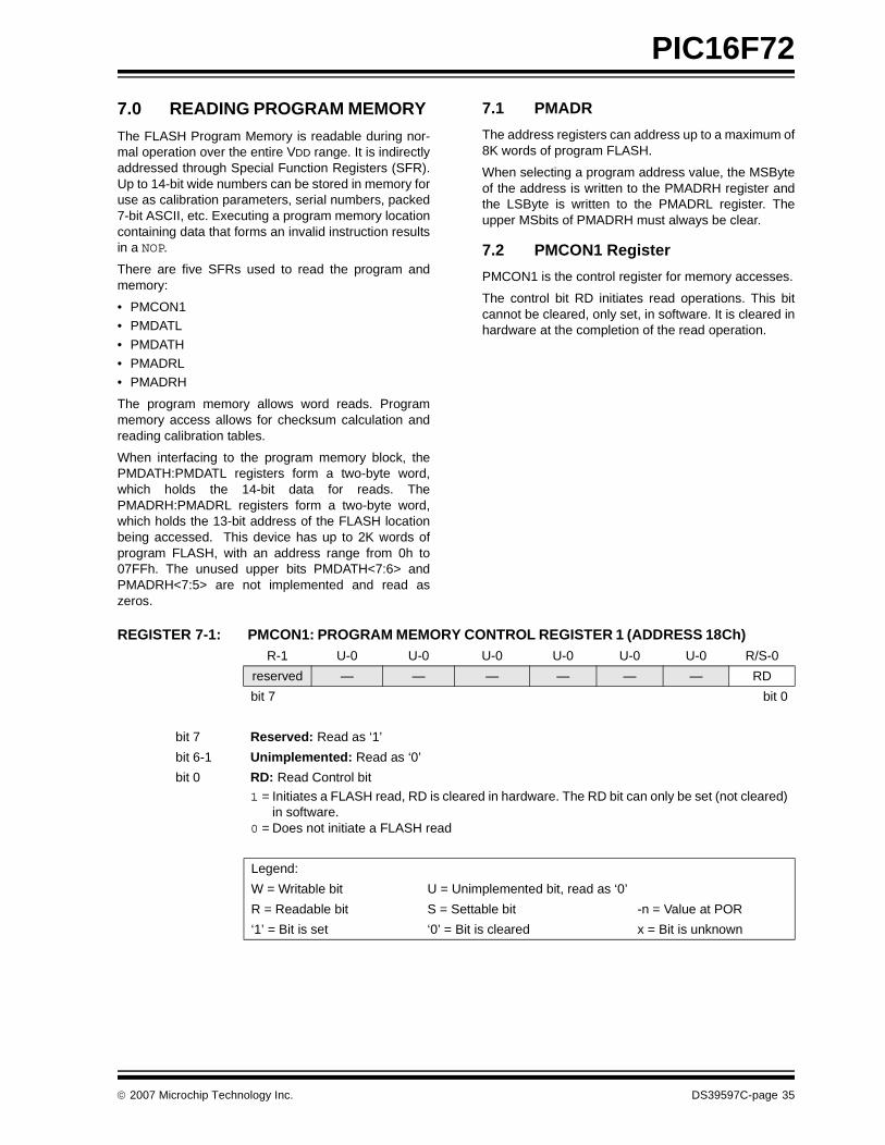
PIC16F72
7.0 READING PROGRAM MEMORY
The FLASH Program Memory is readable during nor-mal operation over the entire VDD range. It is indirectlyaddressed through Special Function Registers (SFR).Up to 14-bit wide numbers can be stored in memory foruse as calibration parameters, serial numbers, packed7-bit ASCII, etc. Executing a program memory locationcontaining data that forms an invalid instruction resultsin a NOP.
There are five SFRs used to read the program andmemory:
• PMCON1• PMDATL
• PMDATH• PMADRL• PMADRH
The program memory allows word reads. Programmemory access allows for checksum calculation andreading calibration tables.
When interfacing to the program memory block, thePMDATH:PMDATL registers form a two-byte word,which holds the 14-bit data for reads. ThePMADRH:PMADRL registers form a two-byte word,which holds the 13-bit address of the FLASH locationbeing accessed. This device has up to 2K words ofprogram FLASH, with an address range from 0h to07FFh. The unused upper bits PMDATH<7:6> andPMADRH<7:5> are not implemented and read aszeros.
7.1 PMADR
The address registers can address up to a maximum of8K words of program FLASH.
When selecting a program address value, the MSByteof the address is written to the PMADRH register andthe LSByte is written to the PMADRL register. Theupper MSbits of PMADRH must always be clear.
7.2 PMCON1 Register
PMCON1 is the control register for memory accesses.
The control bit RD initiates read operations. This bitcannot be cleared, only set, in software. It is cleared inhardware at the completion of the read operation.
REGISTER 7-1: PMCON1: PROGRAM MEMORY CONTROL REGISTER 1 (ADDRESS 18Ch) R-1 U-0 U-0 U-0 U-0 U-0 U-0 R/S-0
reserved — — — — — — RD
bit 7 bit 0
bit 7 Reserved: Read as ‘1’
bit 6-1 Unimplemented: Read as ‘0’
bit 0 RD: Read Control bit
1 = Initiates a FLASH read, RD is cleared in hardware. The RD bit can only be set (not cleared)in software.
0 = Does not initiate a FLASH read
Legend:
W = Writable bit U = Unimplemented bit, read as ‘0’
R = Readable bit S = Settable bit -n = Value at POR
‘1’ = Bit is set ‘0’ = Bit is cleared x = Bit is unknown
© 2007 Microchip Technology Inc. DS39597C-page 35
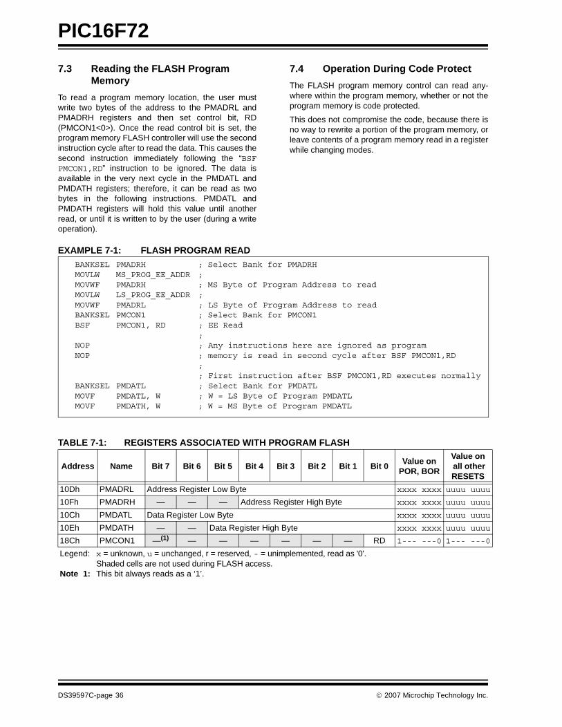
PIC16F72
7.3 Reading the FLASH Program Memory
To read a program memory location, the user mustwrite two bytes of the address to the PMADRL andPMADRH registers and then set control bit, RD(PMCON1<0>). Once the read control bit is set, theprogram memory FLASH controller will use the secondinstruction cycle after to read the data. This causes thesecond instruction immediately following the “BSFPMCON1,RD” instruction to be ignored. The data isavailable in the very next cycle in the PMDATL andPMDATH registers; therefore, it can be read as twobytes in the following instructions. PMDATL andPMDATH registers will hold this value until anotherread, or until it is written to by the user (during a writeoperation).
7.4 Operation During Code Protect
The FLASH program memory control can read any-where within the program memory, whether or not theprogram memory is code protected.
This does not compromise the code, because there isno way to rewrite a portion of the program memory, orleave contents of a program memory read in a registerwhile changing modes.
EXAMPLE 7-1: FLASH PROGRAM READ
TABLE 7-1: REGISTERS ASSOCIATED WITH PROGRAM FLASH
BANKSEL PMADRH ; Select Bank for PMADRHMOVLW MS_PROG_EE_ADDR ;MOVWF PMADRH ; MS Byte of Program Address to readMOVLW LS_PROG_EE_ADDR ;MOVWF PMADRL ; LS Byte of Program Address to readBANKSEL PMCON1 ; Select Bank for PMCON1BSF PMCON1, RD ; EE Read
;NOP ; Any instructions here are ignored as programNOP ; memory is read in second cycle after BSF PMCON1,RD
; ; First instruction after BSF PMCON1,RD executes normally
BANKSEL PMDATL ; Select Bank for PMDATLMOVF PMDATL, W ; W = LS Byte of Program PMDATLMOVF PMDATH, W ; W = MS Byte of Program PMDATL
Address Name Bit 7 Bit 6 Bit 5 Bit 4 Bit 3 Bit 2 Bit 1 Bit 0Value on
POR, BOR
Value on all other RESETS
10Dh PMADRL Address Register Low Byte xxxx xxxx uuuu uuuu
10Fh PMADRH — — — Address Register High Byte xxxx xxxx uuuu uuuu
10Ch PMDATL Data Register Low Byte xxxx xxxx uuuu uuuu
10Eh PMDATH — — Data Register High Byte xxxx xxxx uuuu uuuu
18Ch PMCON1 —(1) — — — — — — RD 1--- ---0 1--- ---0
Legend: x = unknown, u = unchanged, r = reserved, - = unimplemented, read as '0'. Shaded cells are not used during FLASH access.
Note 1: This bit always reads as a ‘1’.
DS39597C-page 36 © 2007 Microchip Technology Inc.
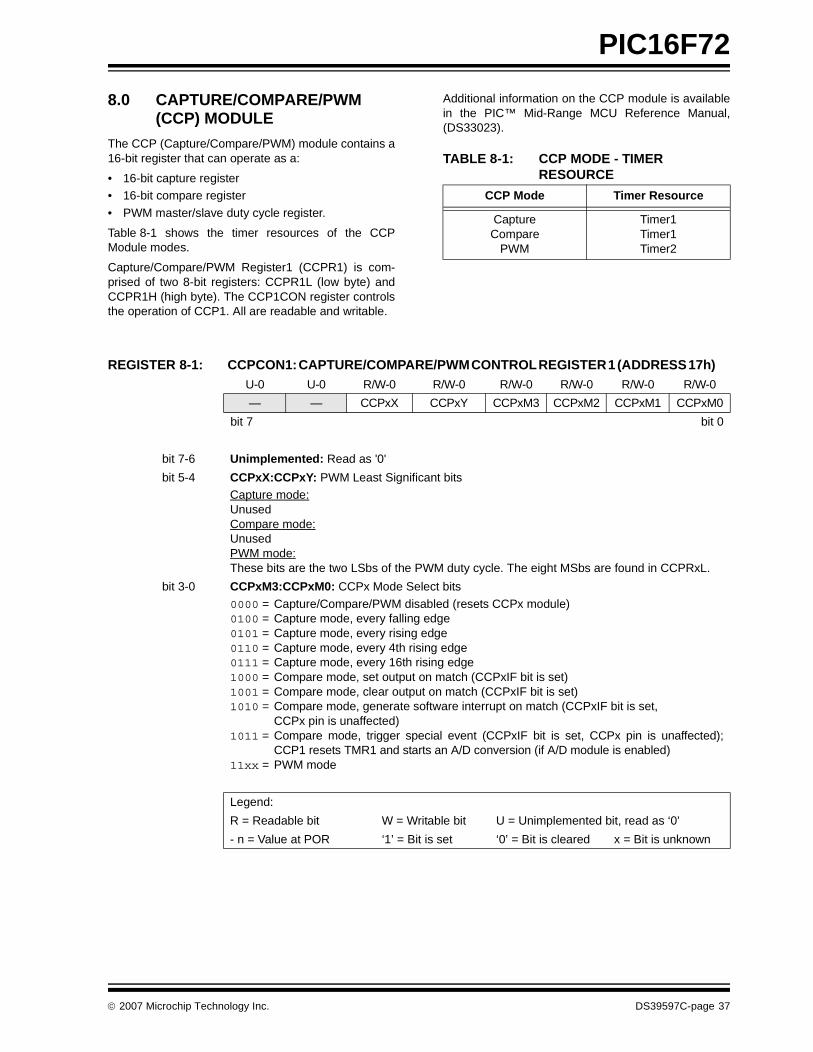
PIC16F72
8.0 CAPTURE/COMPARE/PWM (CCP) MODULE
The CCP (Capture/Compare/PWM) module contains a16-bit register that can operate as a:
• 16-bit capture register• 16-bit compare register
• PWM master/slave duty cycle register.
Table 8-1 shows the timer resources of the CCPModule modes.
Capture/Compare/PWM Register1 (CCPR1) is com-prised of two 8-bit registers: CCPR1L (low byte) andCCPR1H (high byte). The CCP1CON register controlsthe operation of CCP1. All are readable and writable.
Additional information on the CCP module is availablein the PIC™ Mid-Range MCU Reference Manual,(DS33023).
TABLE 8-1: CCP MODE - TIMER RESOURCE
REGISTER 8-1: CCPCON1: CAPTURE/COMPARE/PWM CONTROL REGISTER 1 (ADDRESS 17h)
CCP Mode Timer Resource
CaptureCompare
PWM
Timer1Timer1Timer2
U-0 U-0 R/W-0 R/W-0 R/W-0 R/W-0 R/W-0 R/W-0
— — CCPxX CCPxY CCPxM3 CCPxM2 CCPxM1 CCPxM0
bit 7 bit 0
bit 7-6 Unimplemented: Read as '0'
bit 5-4 CCPxX:CCPxY: PWM Least Significant bitsCapture mode:UnusedCompare mode:UnusedPWM mode:These bits are the two LSbs of the PWM duty cycle. The eight MSbs are found in CCPRxL.
bit 3-0 CCPxM3:CCPxM0: CCPx Mode Select bits
0000 = Capture/Compare/PWM disabled (resets CCPx module)0100 = Capture mode, every falling edge0101 = Capture mode, every rising edge0110 = Capture mode, every 4th rising edge0111 = Capture mode, every 16th rising edge1000 = Compare mode, set output on match (CCPxIF bit is set)1001 = Compare mode, clear output on match (CCPxIF bit is set)1010 = Compare mode, generate software interrupt on match (CCPxIF bit is set,
CCPx pin is unaffected)1011 = Compare mode, trigger special event (CCPxIF bit is set, CCPx pin is unaffected);
CCP1 resets TMR1 and starts an A/D conversion (if A/D module is enabled)11xx = PWM mode
Legend:
R = Readable bit W = Writable bit U = Unimplemented bit, read as ‘0’
- n = Value at POR ‘1’ = Bit is set ‘0’ = Bit is cleared x = Bit is unknown
© 2007 Microchip Technology Inc. DS39597C-page 37
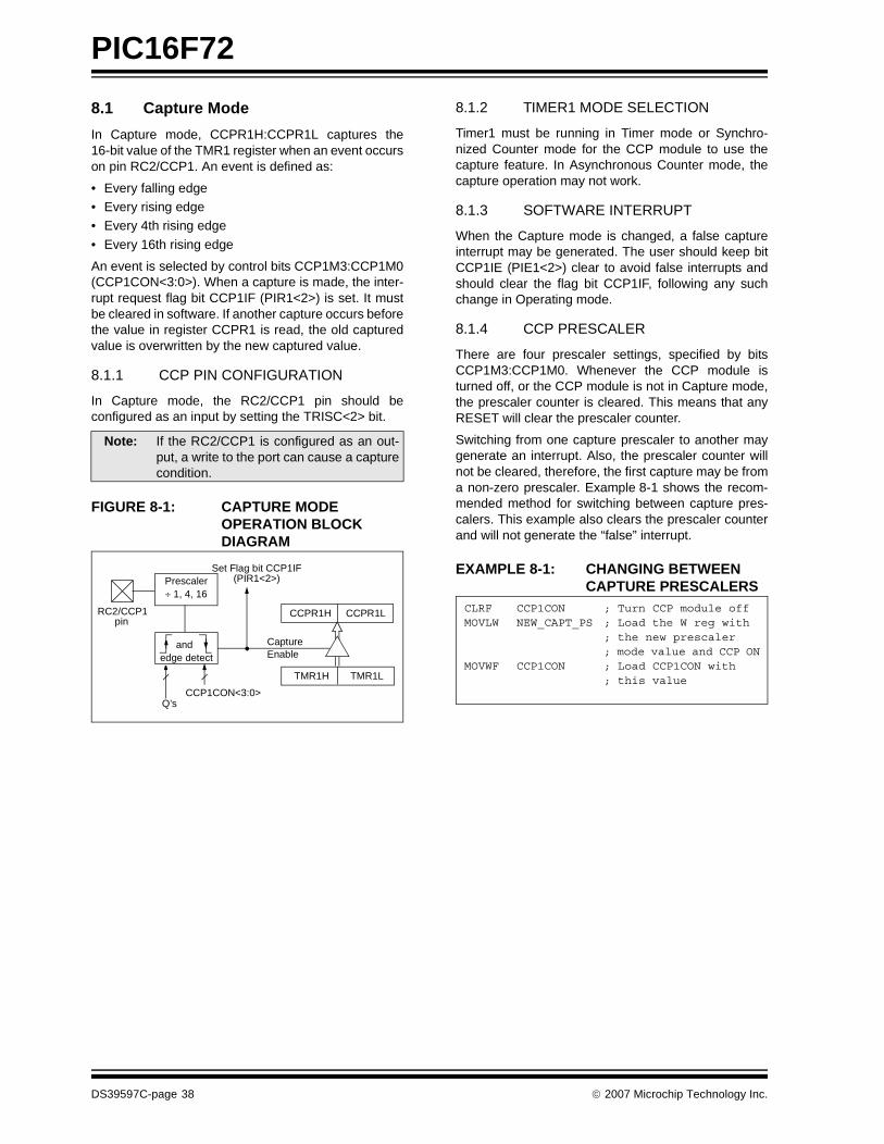
PIC16F72
8.1 Capture Mode
In Capture mode, CCPR1H:CCPR1L captures the16-bit value of the TMR1 register when an event occurson pin RC2/CCP1. An event is defined as:
• Every falling edge• Every rising edge• Every 4th rising edge
• Every 16th rising edge
An event is selected by control bits CCP1M3:CCP1M0(CCP1CON<3:0>). When a capture is made, the inter-rupt request flag bit CCP1IF (PIR1<2>) is set. It mustbe cleared in software. If another capture occurs beforethe value in register CCPR1 is read, the old capturedvalue is overwritten by the new captured value.
8.1.1 CCP PIN CONFIGURATION
In Capture mode, the RC2/CCP1 pin should beconfigured as an input by setting the TRISC<2> bit.
FIGURE 8-1: CAPTURE MODE OPERATION BLOCK DIAGRAM
8.1.2 TIMER1 MODE SELECTION
Timer1 must be running in Timer mode or Synchro-nized Counter mode for the CCP module to use thecapture feature. In Asynchronous Counter mode, thecapture operation may not work.
8.1.3 SOFTWARE INTERRUPT
When the Capture mode is changed, a false captureinterrupt may be generated. The user should keep bitCCP1IE (PIE1<2>) clear to avoid false interrupts andshould clear the flag bit CCP1IF, following any suchchange in Operating mode.
8.1.4 CCP PRESCALER
There are four prescaler settings, specified by bitsCCP1M3:CCP1M0. Whenever the CCP module isturned off, or the CCP module is not in Capture mode,the prescaler counter is cleared. This means that anyRESET will clear the prescaler counter.
Switching from one capture prescaler to another maygenerate an interrupt. Also, the prescaler counter willnot be cleared, therefore, the first capture may be froma non-zero prescaler. Example 8-1 shows the recom-mended method for switching between capture pres-calers. This example also clears the prescaler counterand will not generate the “false” interrupt.
EXAMPLE 8-1: CHANGING BETWEEN CAPTURE PRESCALERS
Note: If the RC2/CCP1 is configured as an out-put, a write to the port can cause a capturecondition.
CCPR1H CCPR1L
TMR1H TMR1L
Set Flag bit CCP1IF(PIR1<2>)
CaptureEnable
Q’sCCP1CON<3:0>
RC2/CCP1
Prescaler÷ 1, 4, 16
andedge detect
pinCLRF CCP1CON ; Turn CCP module offMOVLW NEW_CAPT_PS ; Load the W reg with ; the new prescaler ; mode value and CCP ONMOVWF CCP1CON ; Load CCP1CON with
; this value
DS39597C-page 38 © 2007 Microchip Technology Inc.
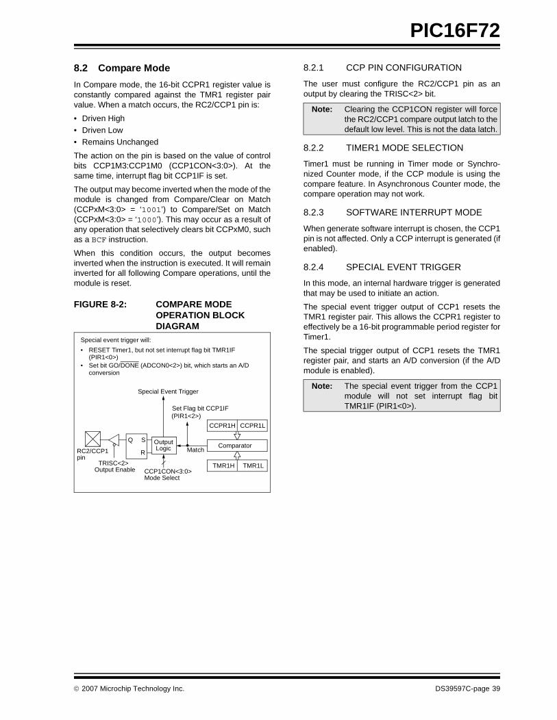
PIC16F72
8.2 Compare Mode
In Compare mode, the 16-bit CCPR1 register value isconstantly compared against the TMR1 register pairvalue. When a match occurs, the RC2/CCP1 pin is:
• Driven High• Driven Low• Remains Unchanged
The action on the pin is based on the value of controlbits CCP1M3:CCP1M0 (CCP1CON<3:0>). At thesame time, interrupt flag bit CCP1IF is set.
The output may become inverted when the mode of themodule is changed from Compare/Clear on Match(CCPxM<3:0> = ‘1001’) to Compare/Set on Match(CCPxM<3:0> = ‘1000’). This may occur as a result ofany operation that selectively clears bit CCPxM0, suchas a BCF instruction.
When this condition occurs, the output becomesinverted when the instruction is executed. It will remaininverted for all following Compare operations, until themodule is reset.
FIGURE 8-2: COMPARE MODE OPERATION BLOCK DIAGRAM
8.2.1 CCP PIN CONFIGURATION
The user must configure the RC2/CCP1 pin as anoutput by clearing the TRISC<2> bit.
8.2.2 TIMER1 MODE SELECTION
Timer1 must be running in Timer mode or Synchro-nized Counter mode, if the CCP module is using thecompare feature. In Asynchronous Counter mode, thecompare operation may not work.
8.2.3 SOFTWARE INTERRUPT MODE
When generate software interrupt is chosen, the CCP1pin is not affected. Only a CCP interrupt is generated (ifenabled).
8.2.4 SPECIAL EVENT TRIGGER
In this mode, an internal hardware trigger is generatedthat may be used to initiate an action.
The special event trigger output of CCP1 resets theTMR1 register pair. This allows the CCPR1 register toeffectively be a 16-bit programmable period register forTimer1.
The special trigger output of CCP1 resets the TMR1register pair, and starts an A/D conversion (if the A/Dmodule is enabled).
CCPR1H CCPR1L
TMR1H TMR1L
ComparatorQ S
R
OutputLogic
Special Event Trigger
Set Flag bit CCP1IF(PIR1<2>)
MatchRC2/CCP1
TRISC<2>CCP1CON<3:0>Mode Select
Output Enable
pin
Special event trigger will:
• RESET Timer1, but not set interrupt flag bit TMR1IF (PIR1<0>)
• Set bit GO/DONE (ADCON0<2>) bit, which starts an A/Dconversion
Note: Clearing the CCP1CON register will forcethe RC2/CCP1 compare output latch to thedefault low level. This is not the data latch.
Note: The special event trigger from the CCP1module will not set interrupt flag bitTMR1IF (PIR1<0>).
© 2007 Microchip Technology Inc. DS39597C-page 39
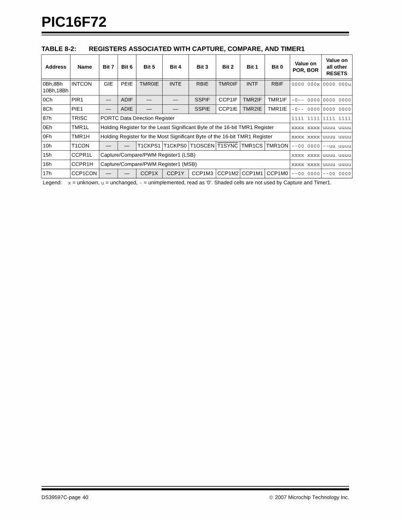
PIC16F72
TABLE 8-2: REGISTERS ASSOCIATED WITH CAPTURE, COMPARE, AND TIMER1
Address Name Bit 7 Bit 6 Bit 5 Bit 4 Bit 3 Bit 2 Bit 1 Bit 0Value on
POR, BOR
Value onall otherRESETS
0Bh,8Bh10Bh,18Bh
INTCON GIE PEIE TMR0IE INTE RBIE TMR0IF INTF RBIF 0000 000x 0000 000u
0Ch PIR1 — ADIF — — SSPIF CCP1IF TMR2IF TMR1IF -0-- 0000 0000 0000
8Ch PIE1 — ADIE — — SSPIE CCP1IE TMR2IE TMR1IE -0-- 0000 0000 0000
87h TRISC PORTC Data Direction Register 1111 1111 1111 1111
0Eh TMR1L Holding Register for the Least Significant Byte of the 16-bit TMR1 Register xxxx xxxx uuuu uuuu
0Fh TMR1H Holding Register for the Most Significant Byte of the 16-bit TMR1 Register xxxx xxxx uuuu uuuu
10h T1CON — — T1CKPS1 T1CKPS0 T1OSCEN T1SYNC TMR1CS TMR1ON --00 0000 --uu uuuu
15h CCPR1L Capture/Compare/PWM Register1 (LSB) xxxx xxxx uuuu uuuu
16h CCPR1H Capture/Compare/PWM Register1 (MSB) xxxx xxxx uuuu uuuu
17h CCP1CON — — CCP1X CCP1Y CCP1M3 CCP1M2 CCP1M1 CCP1M0 --00 0000 --00 0000
Legend: x = unknown, u = unchanged, - = unimplemented, read as ‘0’. Shaded cells are not used by Capture and Timer1.
DS39597C-page 40 © 2007 Microchip Technology Inc.
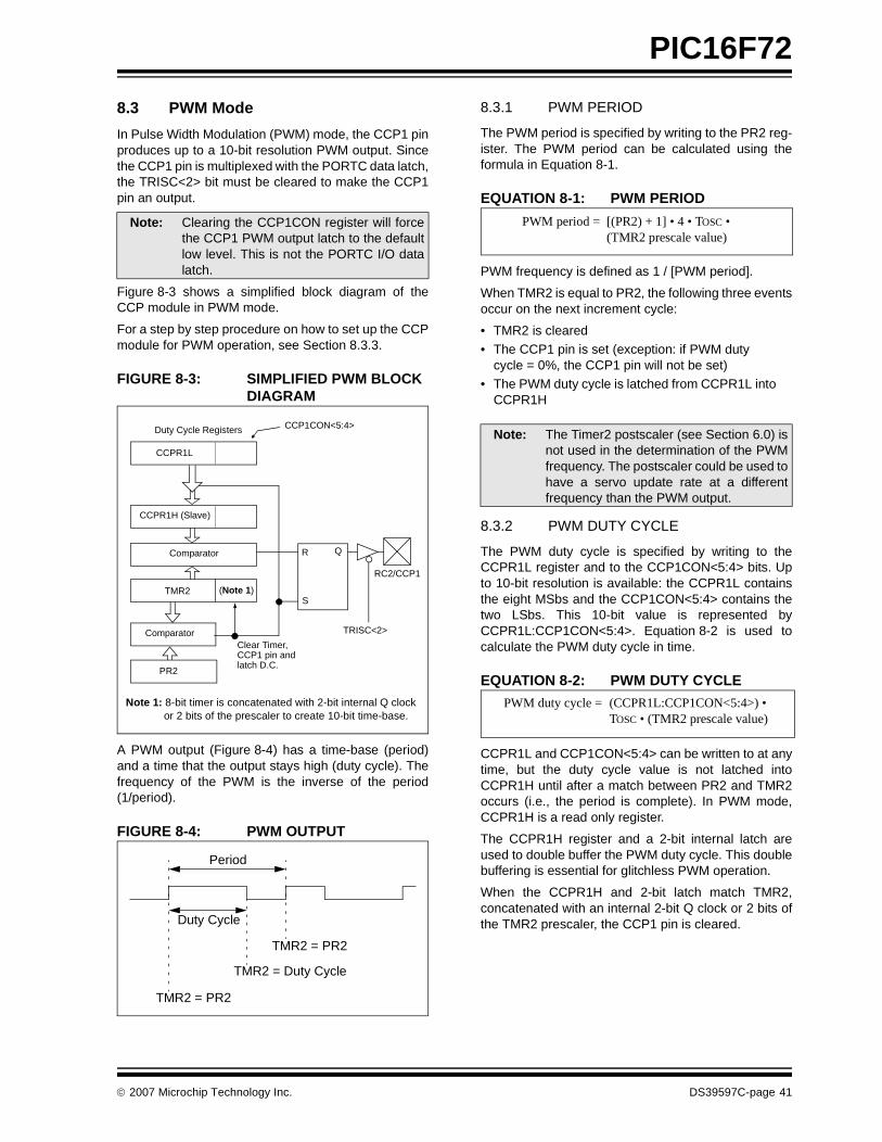
PIC16F72
8.3 PWM Mode
In Pulse Width Modulation (PWM) mode, the CCP1 pinproduces up to a 10-bit resolution PWM output. Sincethe CCP1 pin is multiplexed with the PORTC data latch,the TRISC<2> bit must be cleared to make the CCP1pin an output.
Figure 8-3 shows a simplified block diagram of theCCP module in PWM mode.
For a step by step procedure on how to set up the CCPmodule for PWM operation, see Section 8.3.3.
FIGURE 8-3: SIMPLIFIED PWM BLOCK DIAGRAM
A PWM output (Figure 8-4) has a time-base (period)and a time that the output stays high (duty cycle). Thefrequency of the PWM is the inverse of the period(1/period).
FIGURE 8-4: PWM OUTPUT
8.3.1 PWM PERIOD
The PWM period is specified by writing to the PR2 reg-ister. The PWM period can be calculated using theformula in Equation 8-1.
EQUATION 8-1: PWM PERIOD
PWM frequency is defined as 1 / [PWM period].
When TMR2 is equal to PR2, the following three eventsoccur on the next increment cycle:
• TMR2 is cleared• The CCP1 pin is set (exception: if PWM duty
cycle = 0%, the CCP1 pin will not be set)• The PWM duty cycle is latched from CCPR1L into
CCPR1H
8.3.2 PWM DUTY CYCLE
The PWM duty cycle is specified by writing to theCCPR1L register and to the CCP1CON<5:4> bits. Upto 10-bit resolution is available: the CCPR1L containsthe eight MSbs and the CCP1CON<5:4> contains thetwo LSbs. This 10-bit value is represented byCCPR1L:CCP1CON<5:4>. Equation 8-2 is used tocalculate the PWM duty cycle in time.
EQUATION 8-2: PWM DUTY CYCLE
CCPR1L and CCP1CON<5:4> can be written to at anytime, but the duty cycle value is not latched intoCCPR1H until after a match between PR2 and TMR2occurs (i.e., the period is complete). In PWM mode,CCPR1H is a read only register.
The CCPR1H register and a 2-bit internal latch areused to double buffer the PWM duty cycle. This doublebuffering is essential for glitchless PWM operation.
When the CCPR1H and 2-bit latch match TMR2,concatenated with an internal 2-bit Q clock or 2 bits ofthe TMR2 prescaler, the CCP1 pin is cleared.
Note: Clearing the CCP1CON register will forcethe CCP1 PWM output latch to the defaultlow level. This is not the PORTC I/O datalatch.
CCPR1L
CCPR1H (Slave)
Comparator
TMR2
Comparator
PR2
(Note 1)
R Q
S
Duty Cycle Registers CCP1CON<5:4>
Clear Timer,CCP1 pin and latch D.C.
TRISC<2>
RC2/CCP1
Note 1: 8-bit timer is concatenated with 2-bit internal Q clockor 2 bits of the prescaler to create 10-bit time-base.
Period
Duty Cycle
TMR2 = PR2
TMR2 = Duty Cycle
TMR2 = PR2
Note: The Timer2 postscaler (see Section 6.0) isnot used in the determination of the PWMfrequency. The postscaler could be used tohave a servo update rate at a differentfrequency than the PWM output.
PWM period = [(PR2) + 1] • 4 • TOSC •(TMR2 prescale value)
PWM duty cycle = (CCPR1L:CCP1CON<5:4>) •TOSC • (TMR2 prescale value)
© 2007 Microchip Technology Inc. DS39597C-page 41
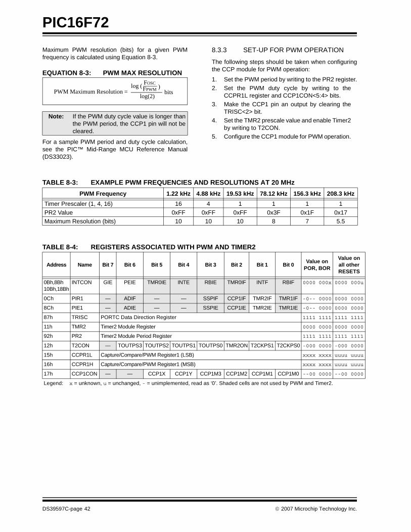
PIC16F72
Maximum PWM resolution (bits) for a given PWMfrequency is calculated using Equation 8-3.
EQUATION 8-3: PWM MAX RESOLUTION
For a sample PWM period and duty cycle calculation,see the PIC™ Mid-Range MCU Reference Manual(DS33023).
8.3.3 SET-UP FOR PWM OPERATION
The following steps should be taken when configuringthe CCP module for PWM operation:
1. Set the PWM period by writing to the PR2 register.2. Set the PWM duty cycle by writing to the
CCPR1L register and CCP1CON<5:4> bits.3. Make the CCP1 pin an output by clearing the
TRISC<2> bit.4. Set the TMR2 prescale value and enable Timer2
by writing to T2CON.5. Configure the CCP1 module for PWM operation.
TABLE 8-3: EXAMPLE PWM FREQUENCIES AND RESOLUTIONS AT 20 MHz
TABLE 8-4: REGISTERS ASSOCIATED WITH PWM AND TIMER2
Note: If the PWM duty cycle value is longer thanthe PWM period, the CCP1 pin will not becleared.
log ( FPWM
log(2)
FOSC )
bitsPWM Maximum Resolution =
PWM Frequency 1.22 kHz 4.88 kHz 19.53 kHz 78.12 kHz 156.3 kHz 208.3 kHz
Timer Prescaler (1, 4, 16) 16 4 1 1 1 1
PR2 Value 0xFF 0xFF 0xFF 0x3F 0x1F 0x17Maximum Resolution (bits) 10 10 10 8 7 5.5
Address Name Bit 7 Bit 6 Bit 5 Bit 4 Bit 3 Bit 2 Bit 1 Bit 0Value on
POR, BOR
Value on all otherRESETS
0Bh,8Bh10Bh,18Bh
INTCON GIE PEIE TMR0IE INTE RBIE TMR0IF INTF RBIF 0000 000x 0000 000u
0Ch PIR1 — ADIF — — SSPIF CCP1IF TMR2IF TMR1IF -0-- 0000 0000 0000
8Ch PIE1 — ADIE — — SSPIE CCP1IE TMR2IE TMR1IE -0-- 0000 0000 0000
87h TRISC PORTC Data Direction Register 1111 1111 1111 1111
11h TMR2 Timer2 Module Register 0000 0000 0000 0000
92h PR2 Timer2 Module Period Register 1111 1111 1111 1111
12h T2CON — TOUTPS3 TOUTPS2 TOUTPS1 TOUTPS0 TMR2ON T2CKPS1 T2CKPS0 -000 0000 -000 0000
15h CCPR1L Capture/Compare/PWM Register1 (LSB) xxxx xxxx uuuu uuuu
16h CCPR1H Capture/Compare/PWM Register1 (MSB) xxxx xxxx uuuu uuuu
17h CCP1CON — — CCP1X CCP1Y CCP1M3 CCP1M2 CCP1M1 CCP1M0 --00 0000 --00 0000
Legend: x = unknown, u = unchanged, - = unimplemented, read as ‘0’. Shaded cells are not used by PWM and Timer2.
DS39597C-page 42 © 2007 Microchip Technology Inc.
PIC16F72
9.0 SYNCHRONOUS SERIAL PORT (SSP) MODULE
9.1 SSP Module Overview
The Synchronous Serial Port (SSP) module is a serialinterface useful for communicating with other periph-eral or microcontroller devices. These peripheraldevices may be Serial EEPROMs, shift registers, dis-play drivers, A/D converters, etc. The SSP module canoperate in one of two modes:
• Serial Peripheral Interface (SPI)• Inter-Integrated Circuit (I2C)
An overview of I2C operations and additional informa-tion on the SSP module can be found in the PIC™ Mid-Range MCU Family Reference Manual(DS33023).
Refer to Application Note AN578, “Use of the SSPModule in the I 2C Multi-Master Environment.”
9.2 SPI Mode
This section contains register definitions andoperational characteristics of the SPI module.
SPI mode allows 8 bits of data to be synchronouslytransmitted and received simultaneously. To accomplishcommunication, typically three pins are used:
• Serial Data Out (SDO) RC5/SDO
• Serial Data In (SDI) RC4/SDI/SDA• Serial Clock (SCK) RC3/SCK/SCL
Additionally, a fourth pin may be used when in a Slavemode of operation:
• Slave Select (SS) RA5/AN4/SS
When initializing the SPI, several options need to bespecified. This is done by programming the appropriatecontrol bits in the SSPCON register (SSPCON<5:0>)and SSPSTAT<7:6>. These control bits allow thefollowing to be specified:
• Master mode (SCK is the clock output)
• Slave mode (SCK is the clock input)• Clock Polarity (IDLE state of SCK)• Clock edge (output data on rising/falling edge of
SCK)• Clock Rate (Master mode only)
• Slave Select mode (Slave mode only)
© 2007 Microchip Technology Inc. DS39597C-page 43
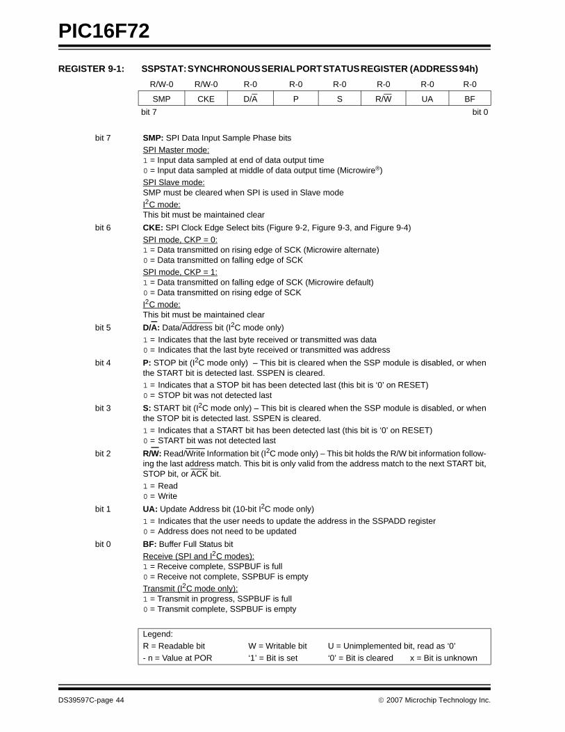
PIC16F72
REGISTER 9-1: SSPSTAT: SYNCHRONOUS SERIAL PORT STATUS REGISTER (ADDRESS 94h)
R/W-0 R/W-0 R-0 R-0 R-0 R-0 R-0 R-0
SMP CKE D/A P S R/W UA BF
bit 7 bit 0
bit 7 SMP: SPI Data Input Sample Phase bitsSPI Master mode:1 = Input data sampled at end of data output time0 = Input data sampled at middle of data output time (Microwire®)SPI Slave mode:SMP must be cleared when SPI is used in Slave modeI2 C mode:This bit must be maintained clear
bit 6 CKE: SPI Clock Edge Select bits (Figure 9-2, Figure 9-3, and Figure 9-4)
SPI mode, CKP = 0:1 = Data transmitted on rising edge of SCK (Microwire alternate)0 = Data transmitted on falling edge of SCKSPI mode, CKP = 1:1 = Data transmitted on falling edge of SCK (Microwire default)0 = Data transmitted on rising edge of SCKI2 C mode:This bit must be maintained clear
bit 5 D/A: Data/Address bit (I2C mode only)
1 = Indicates that the last byte received or transmitted was data0 = Indicates that the last byte received or transmitted was address
bit 4 P: STOP bit (I2C mode only) – This bit is cleared when the SSP module is disabled, or whenthe START bit is detected last. SSPEN is cleared.1 = Indicates that a STOP bit has been detected last (this bit is ‘0’ on RESET)0 = STOP bit was not detected last
bit 3 S: START bit (I2C mode only) – This bit is cleared when the SSP module is disabled, or whenthe STOP bit is detected last. SSPEN is cleared.1 = Indicates that a START bit has been detected last (this bit is ‘0’ on RESET)0 = START bit was not detected last
bit 2 R/W: Read/Write Information bit (I2C mode only) – This bit holds the R/W bit information follow-ing the last address match. This bit is only valid from the address match to the next START bit,STOP bit, or ACK bit.1 = Read0 = Write
bit 1 UA: Update Address bit (10-bit I2C mode only)1 = Indicates that the user needs to update the address in the SSPADD register0 = Address does not need to be updated
bit 0 BF: Buffer Full Status bit
Receive (SPI and I2 C modes):1 = Receive complete, SSPBUF is full0 = Receive not complete, SSPBUF is emptyTransmit (I2 C mode only):1 = Transmit in progress, SSPBUF is full0 = Transmit complete, SSPBUF is empty
Legend:R = Readable bit W = Writable bit U = Unimplemented bit, read as ‘0’- n = Value at POR ‘1’ = Bit is set ‘0’ = Bit is cleared x = Bit is unknown
DS39597C-page 44 © 2007 Microchip Technology Inc.
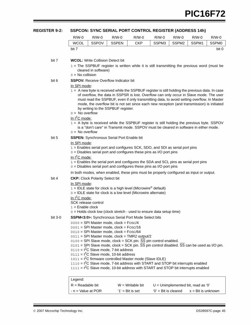
PIC16F72
REGISTER 9-2: SSPCON: SYNC SERIAL PORT CONTROL REGISTER (ADDRESS 14h)
R/W-0 R/W-0 R/W-0 R/W-0 R/W-0 R/W-0 R/W-0 R/W-0
WCOL SSPOV SSPEN CKP SSPM3 SSPM2 SSPM1 SSPM0
bit 7 bit 0
bit 7 WCOL: Write Collision Detect bit
1 = The SSPBUF register is written while it is still transmitting the previous word (must becleared in software)
0 = No collision
bit 6 SSPOV: Receive Overflow Indicator bitIn SPI mode:1 = A new byte is received while the SSPBUF register is still holding the previous data. In case
of overflow, the data in SSPSR is lost. Overflow can only occur in Slave mode. The usermust read the SSPBUF, even if only transmitting data, to avoid setting overflow. In Mastermode, the overflow bit is not set since each new reception (and transmission) is initiatedby writing to the SSPBUF register.
0 = No overflowIn I2 C mode:1 = A byte is received while the SSPBUF register is still holding the previous byte. SSPOV
is a "don’t care" in Transmit mode. SSPOV must be cleared in software in either mode.0 = No overflow
bit 5 SSPEN: Synchronous Serial Port Enable bitIn SPI mode:1 = Enables serial port and configures SCK, SDO, and SDI as serial port pins0 = Disables serial port and configures these pins as I/O port pinsIn I2 C mode:1 = Enables the serial port and configures the SDA and SCL pins as serial port pins0 = Disables serial port and configures these pins as I/O port pins
In both modes, when enabled, these pins must be properly configured as input or output.
bit 4 CKP: Clock Polarity Select bitIn SPI mode:1 = IDLE state for clock is a high level (Microwire® default)0 = IDLE state for clock is a low level (Microwire alternate)In I2 C mode:SCK release control1 = Enable clock0 = Holds clock low (clock stretch - used to ensure data setup time)
bit 3-0 SSPM<3:0>: Synchronous Serial Port Mode Select bits0000 = SPI Master mode, clock = FOSC/40001 = SPI Master mode, clock = FOSC/160010 = SPI Master mode, clock = FOSC/640011 = SPI Master mode, clock = TMR2 output/20100 = SPI Slave mode, clock = SCK pin. SS pin control enabled.0101 = SPI Slave mode, clock = SCK pin. SS pin control disabled. SS can be used as I/O pin.0110 = I2C Slave mode, 7-bit address0111 = I2C Slave mode, 10-bit address1011 = I2C firmware controlled Master mode (Slave IDLE)1110 = I2C Slave mode, 7-bit address with START and STOP bit interrupts enabled1111 = I2C Slave mode, 10-bit address with START and STOP bit interrupts enabled
Legend:
R = Readable bit W = Writable bit U = Unimplemented bit, read as ‘0’
- n = Value at POR ‘1’ = Bit is set ‘0’ = Bit is cleared x = Bit is unknown
© 2007 Microchip Technology Inc. DS39597C-page 45
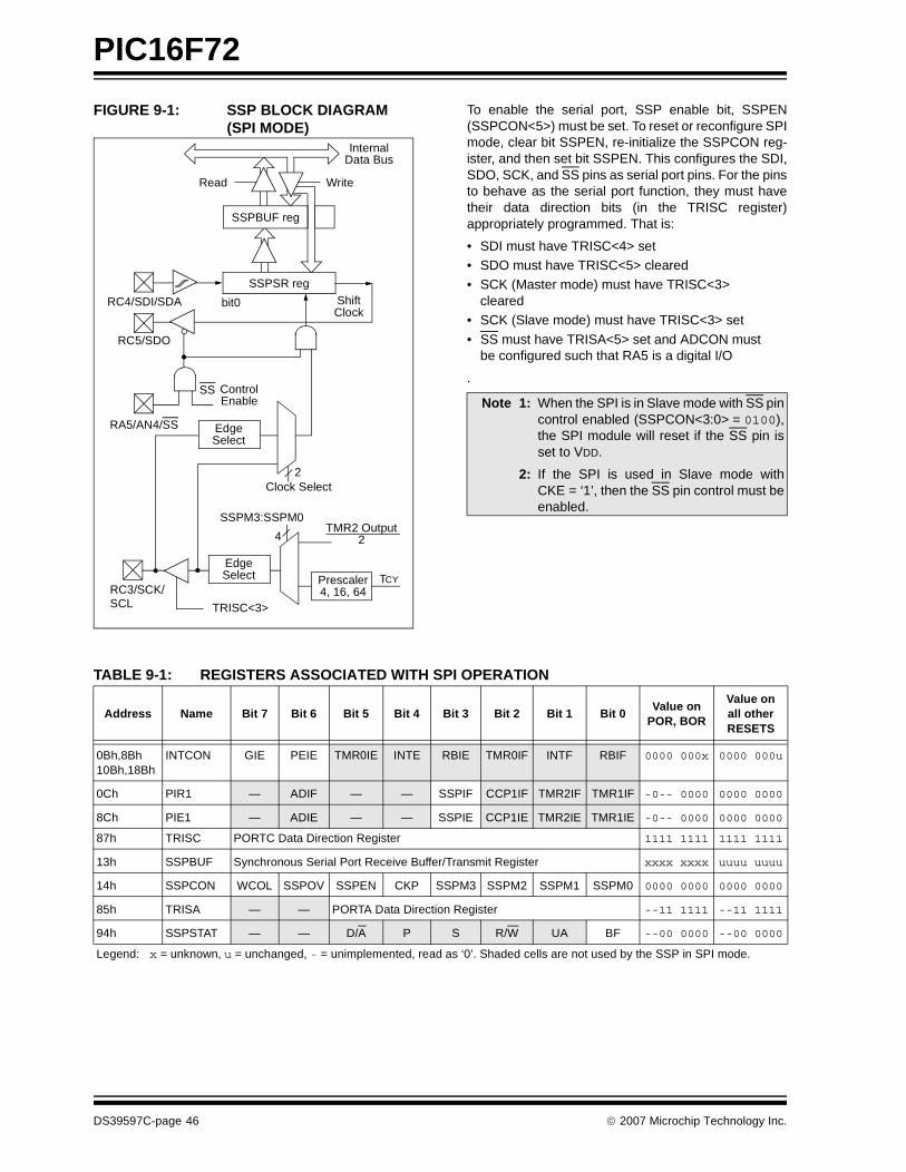
PIC16F72
FIGURE 9-1: SSP BLOCK DIAGRAM (SPI MODE)
To enable the serial port, SSP enable bit, SSPEN(SSPCON<5>) must be set. To reset or reconfigure SPImode, clear bit SSPEN, re-initialize the SSPCON reg-ister, and then set bit SSPEN. This configures the SDI,SDO, SCK, and SS pins as serial port pins. For the pinsto behave as the serial port function, they must havetheir data direction bits (in the TRISC register)appropriately programmed. That is:
• SDI must have TRISC<4> set• SDO must have TRISC<5> cleared• SCK (Master mode) must have TRISC<3>
cleared• SCK (Slave mode) must have TRISC<3> set
• SS must have TRISA<5> set and ADCON must be configured such that RA5 is a digital I/O
.
TABLE 9-1: REGISTERS ASSOCIATED WITH SPI OPERATION
Read Write
InternalData Bus
RC4/SDI/SDA
RC5/SDO
RA5/AN4/SS
RC3/SCK/
SSPSR reg
SSPBUF reg
SSPM3:SSPM0
bit0 ShiftClock
SS ControlEnable
EdgeSelect
Clock Select
TMR2 Output
TCYPrescaler4, 16, 64
TRISC<3>
2
EdgeSelect
2
4
SCL
Note 1: When the SPI is in Slave mode with SS pincontrol enabled (SSPCON<3:0> = 0100),the SPI module will reset if the SS pin isset to VDD.
2: If the SPI is used in Slave mode withCKE = ‘1’, then the SS pin control must beenabled.
Address Name Bit 7 Bit 6 Bit 5 Bit 4 Bit 3 Bit 2 Bit 1 Bit 0Value on
POR, BOR
Value onall otherRESETS
0Bh,8Bh10Bh,18Bh
INTCON GIE PEIE TMR0IE INTE RBIE TMR0IF INTF RBIF 0000 000x 0000 000u
0Ch PIR1 — ADIF — — SSPIF CCP1IF TMR2IF TMR1IF -0-- 0000 0000 0000
8Ch PIE1 — ADIE — — SSPIE CCP1IE TMR2IE TMR1IE -0-- 0000 0000 0000
87h TRISC PORTC Data Direction Register 1111 1111 1111 1111
13h SSPBUF Synchronous Serial Port Receive Buffer/Transmit Register xxxx xxxx uuuu uuuu
14h SSPCON WCOL SSPOV SSPEN CKP SSPM3 SSPM2 SSPM1 SSPM0 0000 0000 0000 0000
85h TRISA — — PORTA Data Direction Register --11 1111 --11 1111
94h SSPSTAT — — D/A P S R/W UA BF --00 0000 --00 0000
Legend: x = unknown, u = unchanged, - = unimplemented, read as ‘0’. Shaded cells are not used by the SSP in SPI mode.
DS39597C-page 46 © 2007 Microchip Technology Inc.
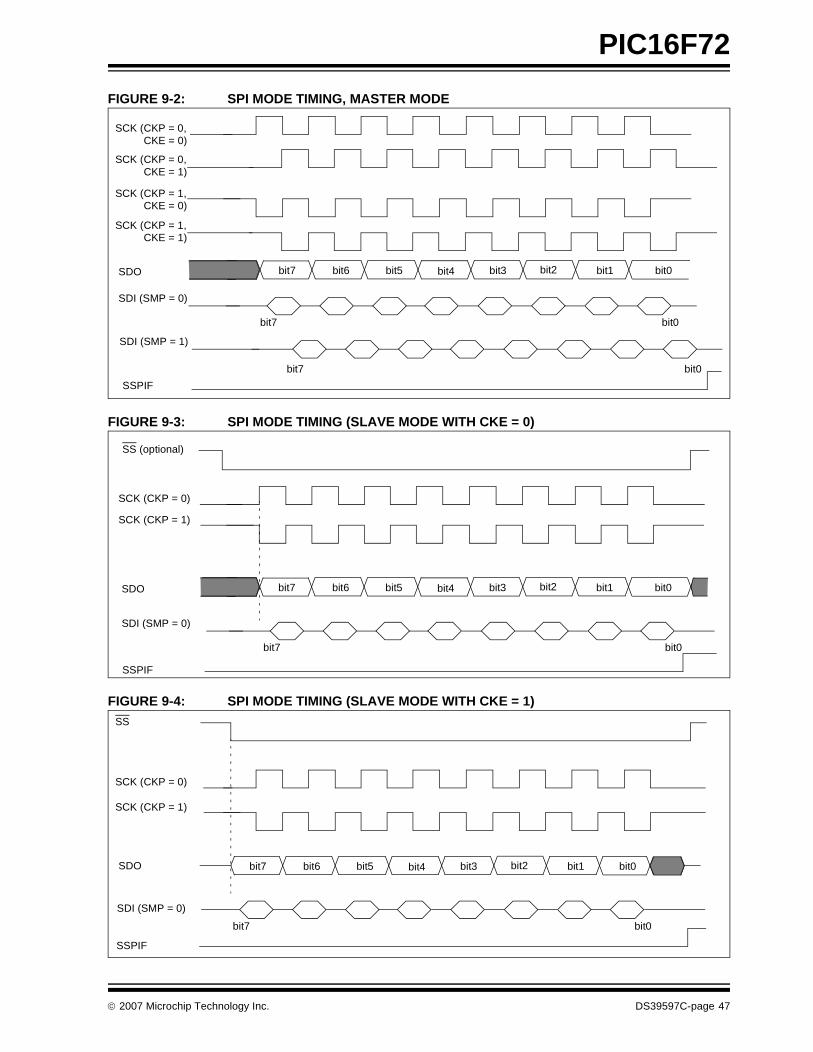
PIC16F72
FIGURE 9-2: SPI MODE TIMING, MASTER MODE
FIGURE 9-3: SPI MODE TIMING (SLAVE MODE WITH CKE = 0)
FIGURE 9-4: SPI MODE TIMING (SLAVE MODE WITH CKE = 1)
SCK (CKP = 0,
SDI (SMP = 0)
SSPIF
bit7 bit6 bit5 bit4 bit3 bit2 bit1 bit0
SDI (SMP = 1)
SCK (CKP = 0,
SCK (CKP = 1,
SCK (CKP = 1,
SDO
bit7
bit7 bit0
bit0
CKE = 0)
CKE = 1)
CKE = 0)
CKE = 1)
SCK (CKP = 0)
SDI (SMP = 0)
SSPIF
bit7 bit6 bit5 bit4 bit3 bit2 bit1 bit0
SCK (CKP = 1)
SDO
bit7 bit0
SS (optional)
SCK (CKP = 0)
SDI (SMP = 0)
SSPIF
bit7 bit6 bit5 bit4 bit3 bit2 bit1 bit0
SCK (CKP = 1)
SDO
bit7 bit0
SS
© 2007 Microchip Technology Inc. DS39597C-page 47
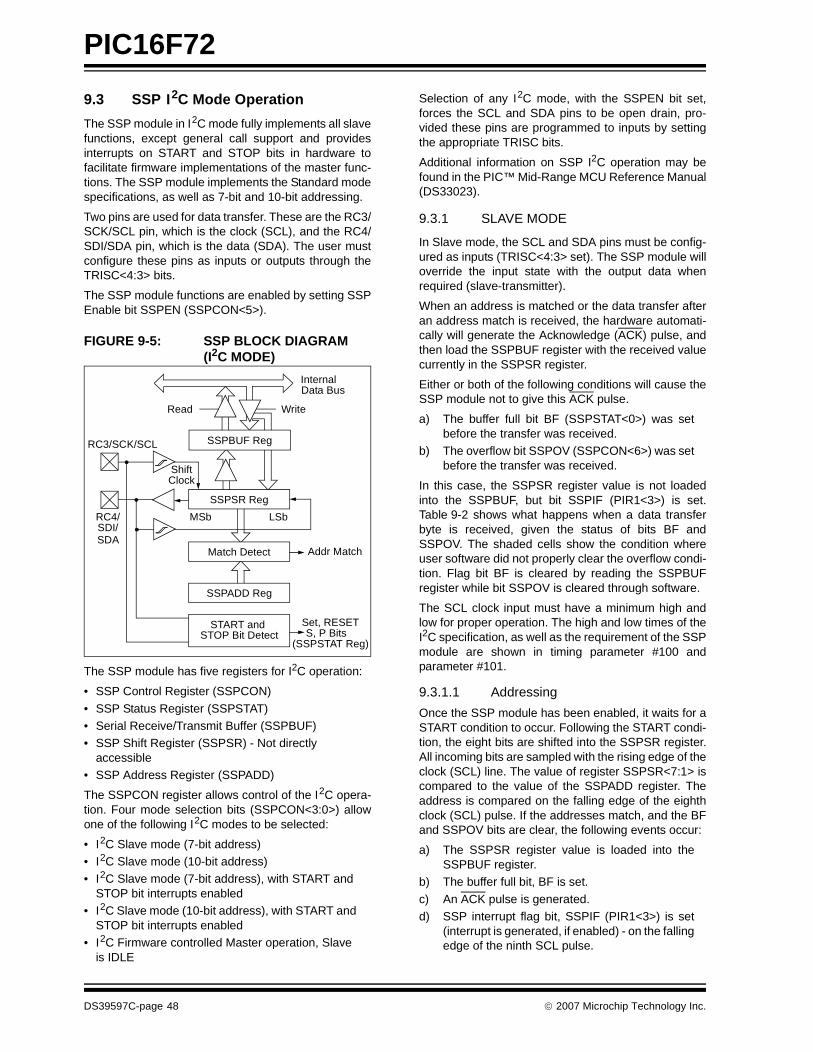
PIC16F72
9.3 SSP I2C Mode Operation
The SSP module in I2C mode fully implements all slavefunctions, except general call support and providesinterrupts on START and STOP bits in hardware tofacilitate firmware implementations of the master func-tions. The SSP module implements the Standard modespecifications, as well as 7-bit and 10-bit addressing.
Two pins are used for data transfer. These are the RC3/SCK/SCL pin, which is the clock (SCL), and the RC4/SDI/SDA pin, which is the data (SDA). The user mustconfigure these pins as inputs or outputs through theTRISC<4:3> bits.
The SSP module functions are enabled by setting SSPEnable bit SSPEN (SSPCON<5>).
FIGURE 9-5: SSP BLOCK DIAGRAM (I2C MODE)
The SSP module has five registers for I2C operation:
• SSP Control Register (SSPCON)
• SSP Status Register (SSPSTAT)• Serial Receive/Transmit Buffer (SSPBUF)• SSP Shift Register (SSPSR) - Not directly
accessible• SSP Address Register (SSPADD)
The SSPCON register allows control of the I2C opera-tion. Four mode selection bits (SSPCON<3:0>) allowone of the following I2C modes to be selected:
• I2C Slave mode (7-bit address)• I2C Slave mode (10-bit address)• I2C Slave mode (7-bit address), with START and
STOP bit interrupts enabled• I2C Slave mode (10-bit address), with START and
STOP bit interrupts enabled• I2C Firmware controlled Master operation, Slave
is IDLE
Selection of any I2C mode, with the SSPEN bit set,forces the SCL and SDA pins to be open drain, pro-vided these pins are programmed to inputs by settingthe appropriate TRISC bits.
Additional information on SSP I2C operation may befound in the PIC™ Mid-Range MCU Reference Manual(DS33023).
9.3.1 SLAVE MODE
In Slave mode, the SCL and SDA pins must be config-ured as inputs (TRISC<4:3> set). The SSP module willoverride the input state with the output data whenrequired (slave-transmitter).
When an address is matched or the data transfer afteran address match is received, the hardware automati-cally will generate the Acknowledge (ACK) pulse, andthen load the SSPBUF register with the received valuecurrently in the SSPSR register.
Either or both of the following conditions will cause theSSP module not to give this ACK pulse.
a) The buffer full bit BF (SSPSTAT<0>) was setbefore the transfer was received.
b) The overflow bit SSPOV (SSPCON<6>) was setbefore the transfer was received.
In this case, the SSPSR register value is not loadedinto the SSPBUF, but bit SSPIF (PIR1<3>) is set.Table 9-2 shows what happens when a data transferbyte is received, given the status of bits BF andSSPOV. The shaded cells show the condition whereuser software did not properly clear the overflow condi-tion. Flag bit BF is cleared by reading the SSPBUFregister while bit SSPOV is cleared through software.
The SCL clock input must have a minimum high andlow for proper operation. The high and low times of theI2C specification, as well as the requirement of the SSPmodule are shown in timing parameter #100 andparameter #101.
9.3.1.1 Addressing
Once the SSP module has been enabled, it waits for aSTART condition to occur. Following the START condi-tion, the eight bits are shifted into the SSPSR register.All incoming bits are sampled with the rising edge of theclock (SCL) line. The value of register SSPSR<7:1> iscompared to the value of the SSPADD register. Theaddress is compared on the falling edge of the eighthclock (SCL) pulse. If the addresses match, and the BFand SSPOV bits are clear, the following events occur:
a) The SSPSR register value is loaded into theSSPBUF register.
b) The buffer full bit, BF is set.
c) An ACK pulse is generated.d) SSP interrupt flag bit, SSPIF (PIR1<3>) is set
(interrupt is generated, if enabled) - on the fallingedge of the ninth SCL pulse.
Read Write
SSPSR Reg
Match Detect
SSPADD Reg
START and STOP Bit Detect
SSPBUF Reg
Internal Data Bus
Addr Match
Set, RESETS, P Bits
(SSPSTAT Reg)
RC3/SCK/SCL
RC4/
ShiftClock
MSbSDI/
LSb
SDA
DS39597C-page 48 © 2007 Microchip Technology Inc.
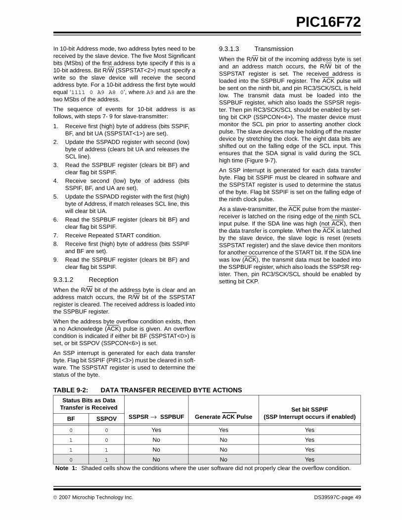
PIC16F72
In 10-bit Address mode, two address bytes need to bereceived by the slave device. The five Most Significantbits (MSbs) of the first address byte specify if this is a10-bit address. Bit R/W (SSPSTAT<2>) must specify awrite so the slave device will receive the secondaddress byte. For a 10-bit address the first byte wouldequal ‘1111 0 A9 A8 0’, where A9 and A8 are thetwo MSbs of the address.
The sequence of events for 10-bit address is asfollows, with steps 7- 9 for slave-transmitter:
1. Receive first (high) byte of address (bits SSPIF,BF, and bit UA (SSPSTAT<1>) are set).
2. Update the SSPADD register with second (low)byte of address (clears bit UA and releases theSCL line).
3. Read the SSPBUF register (clears bit BF) andclear flag bit SSPIF.
4. Receive second (low) byte of address (bitsSSPIF, BF, and UA are set).
5. Update the SSPADD register with the first (high)byte of Address, if match releases SCL line, thiswill clear bit UA.
6. Read the SSPBUF register (clears bit BF) andclear flag bit SSPIF.
7. Receive Repeated START condition.8. Receive first (high) byte of address (bits SSPIF
and BF are set).9. Read the SSPBUF register (clears bit BF) and
clear flag bit SSPIF.
9.3.1.2 Reception
When the R/W bit of the address byte is clear and anaddress match occurs, the R/W bit of the SSPSTATregister is cleared. The received address is loaded intothe SSPBUF register.
When the address byte overflow condition exists, thena no Acknowledge (ACK) pulse is given. An overflowcondition is indicated if either bit BF (SSPSTAT<0>) isset, or bit SSPOV (SSPCON<6>) is set.
An SSP interrupt is generated for each data transferbyte. Flag bit SSPIF (PIR1<3>) must be cleared in soft-ware. The SSPSTAT register is used to determine thestatus of the byte.
9.3.1.3 Transmission
When the R/W bit of the incoming address byte is setand an address match occurs, the R/W bit of theSSPSTAT register is set. The received address isloaded into the SSPBUF register. The ACK pulse willbe sent on the ninth bit, and pin RC3/SCK/SCL is heldlow. The transmit data must be loaded into theSSPBUF register, which also loads the SSPSR regis-ter. Then pin RC3/SCK/SCL should be enabled by set-ting bit CKP (SSPCON<4>). The master device mustmonitor the SCL pin prior to asserting another clockpulse. The slave devices may be holding off the masterdevice by stretching the clock. The eight data bits areshifted out on the falling edge of the SCL input. Thisensures that the SDA signal is valid during the SCLhigh time (Figure 9-7).
An SSP interrupt is generated for each data transferbyte. Flag bit SSPIF must be cleared in software andthe SSPSTAT register is used to determine the statusof the byte. Flag bit SSPIF is set on the falling edge ofthe ninth clock pulse.
As a slave-transmitter, the ACK pulse from the master-receiver is latched on the rising edge of the ninth SCLinput pulse. If the SDA line was high (not ACK), thenthe data transfer is complete. When the ACK is latchedby the slave device, the slave logic is reset (resetsSSPSTAT register) and the slave device then monitorsfor another occurrence of the START bit. If the SDA linewas low (ACK), the transmit data must be loaded intothe SSPBUF register, which also loads the SSPSR reg-ister. Then, pin RC3/SCK/SCL should be enabled bysetting bit CKP.
TABLE 9-2: DATA TRANSFER RECEIVED BYTE ACTIONS
Status Bits as DataTransfer is Received
SSPSR → SSPBUF Generate ACK PulseSet bit SSPIF
(SSP Interrupt occurs if enabled)BF SSPOV
0 0 Yes Yes Yes
1 0 No No Yes
1 1 No No Yes
0 1 No No Yes
Note 1: Shaded cells show the conditions where the user software did not properly clear the overflow condition.
© 2007 Microchip Technology Inc. DS39597C-page 49
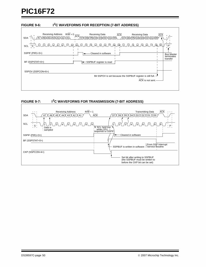
PIC16F72
FIGURE 9-6: I2C WAVEFORMS FOR RECEPTION (7-BIT ADDRESS)
FIGURE 9-7: I2C WAVEFORMS FOR TRANSMISSION (7-BIT ADDRESS)
P98765
D0D1D2D3D4D5D6D7
S
A7 A6 A5 A4 A3 A2 A1SDA
SCL 1 2 3 4 5 6 7 8 9 1 2 3 4 5 6 7 8 9 1 2 3 4
Bus Masterterminatestransfer
Bit SSPOV is set because the SSPBUF register is still full.
Cleared in software
SSPBUF register is read
ACK Receiving DataReceiving Data
D0D1D2D3D4D5D6D7ACK
R/W = 0Receiving Address
SSPIF (PIR1<3>)
BF (SSPSTAT<0>)
SSPOV (SSPCON<6>)
ACK
ACK is not sent.
SDA
SCL
SSPIF (PIR1<3>)
BF (SSPSTAT<0>)
CKP (SSPCON<4>)
A7 A6 A5 A4 A3 A2 A1 ACK D7 D6 D5 D4 D3 D2 D1 D0
ACKTransmitting DataR/W = 1Receiving Address
1 2 3 4 5 6 7 8 9 1 2 3 4 5 6 7 8 9 P
Cleared in software
SSPBUF is written in softwareFrom SSP InterruptService Routine
Set bit after writing to SSPBUF
SData is sampled
SCL held lowwhile CPU
responds to SSPIF
(the SSPBUF must be written tobefore the CKP bit can be set)
DS39597C-page 50 © 2007 Microchip Technology Inc.
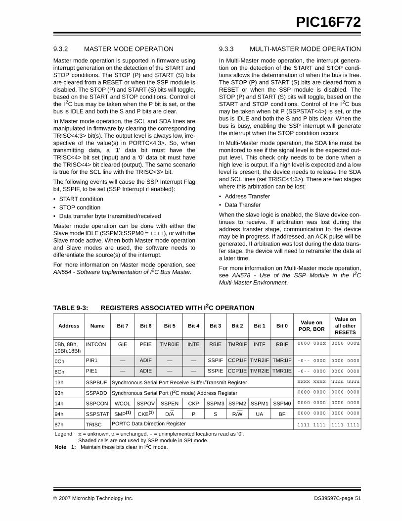
PIC16F72
9.3.2 MASTER MODE OPERATION
Master mode operation is supported in firmware usinginterrupt generation on the detection of the START andSTOP conditions. The STOP (P) and START (S) bitsare cleared from a RESET or when the SSP module isdisabled. The STOP (P) and START (S) bits will toggle,based on the START and STOP conditions. Control ofthe I2C bus may be taken when the P bit is set, or thebus is IDLE and both the S and P bits are clear.
In Master mode operation, the SCL and SDA lines aremanipulated in firmware by clearing the correspondingTRISC<4:3> bit(s). The output level is always low, irre-spective of the value(s) in PORTC<4:3>. So, whentransmitting data, a ‘1’ data bit must have theTRISC<4> bit set (input) and a ‘0’ data bit must havethe TRISC<4> bit cleared (output). The same scenariois true for the SCL line with the TRISC<3> bit.
The following events will cause the SSP Interrupt Flagbit, SSPIF, to be set (SSP Interrupt if enabled):
• START condition• STOP condition
• Data transfer byte transmitted/received
Master mode operation can be done with either theSlave mode IDLE (SSPM3:SSPM0 = 1011), or with theSlave mode active. When both Master mode operationand Slave modes are used, the software needs todifferentiate the source(s) of the interrupt.
For more information on Master mode operation, seeAN554 - Software Implementation of I2C Bus Master.
9.3.3 MULTI-MASTER MODE OPERATION
In Multi-Master mode operation, the interrupt genera-tion on the detection of the START and STOP condi-tions allows the determination of when the bus is free.The STOP (P) and START (S) bits are cleared from aRESET or when the SSP module is disabled. TheSTOP (P) and START (S) bits will toggle, based on theSTART and STOP conditions. Control of the I2C busmay be taken when bit P (SSPSTAT<4>) is set, or thebus is IDLE and both the S and P bits clear. When thebus is busy, enabling the SSP interrupt will generatethe interrupt when the STOP condition occurs.
In Multi-Master mode operation, the SDA line must bemonitored to see if the signal level is the expected out-put level. This check only needs to be done when ahigh level is output. If a high level is expected and a lowlevel is present, the device needs to release the SDAand SCL lines (set TRISC<4:3>). There are two stageswhere this arbitration can be lost:
• Address Transfer• Data Transfer
When the slave logic is enabled, the Slave device con-tinues to receive. If arbitration was lost during theaddress transfer stage, communication to the devicemay be in progress. If addressed, an ACK pulse will begenerated. If arbitration was lost during the data trans-fer stage, the device will need to retransfer the data ata later time.
For more information on Multi-Master mode operation,see AN578 - Use of the SSP Module in the I2CMulti-Master Environment.
TABLE 9-3: REGISTERS ASSOCIATED WITH I2C OPERATION
Address Name Bit 7 Bit 6 Bit 5 Bit 4 Bit 3 Bit 2 Bit 1 Bit 0Value on
POR, BOR
Value on all other RESETS
0Bh, 8Bh,10Bh,18Bh
INTCON GIE PEIE TMR0IE INTE RBIE TMR0IF INTF RBIF 0000 000x 0000 000u
0Ch PIR1 — ADIF — — SSPIF CCP1IF TMR2IF TMR1IF -0-- 0000 0000 0000
8Ch PIE1 — ADIE — — SSPIE CCP1IE TMR2IE TMR1IE -0-- 0000 0000 0000
13h SSPBUF Synchronous Serial Port Receive Buffer/Transmit Register xxxx xxxx uuuu uuuu
93h SSPADD Synchronous Serial Port (I2C mode) Address Register 0000 0000 0000 0000
14h SSPCON WCOL SSPOV SSPEN CKP SSPM3 SSPM2 SSPM1 SSPM0 0000 0000 0000 0000
94h SSPSTAT SMP(1) CKE(1) D/A P S R/W UA BF 0000 0000 0000 0000
87h TRISC PORTC Data Direction Register 1111 1111 1111 1111
Legend: x = unknown, u = unchanged, - = unimplemented locations read as ‘0’. Shaded cells are not used by SSP module in SPI mode.
Note 1: Maintain these bits clear in I2C mode.
© 2007 Microchip Technology Inc. DS39597C-page 51

PIC16F72
NOTES:
DS39597C-page 52 © 2007 Microchip Technology Inc.
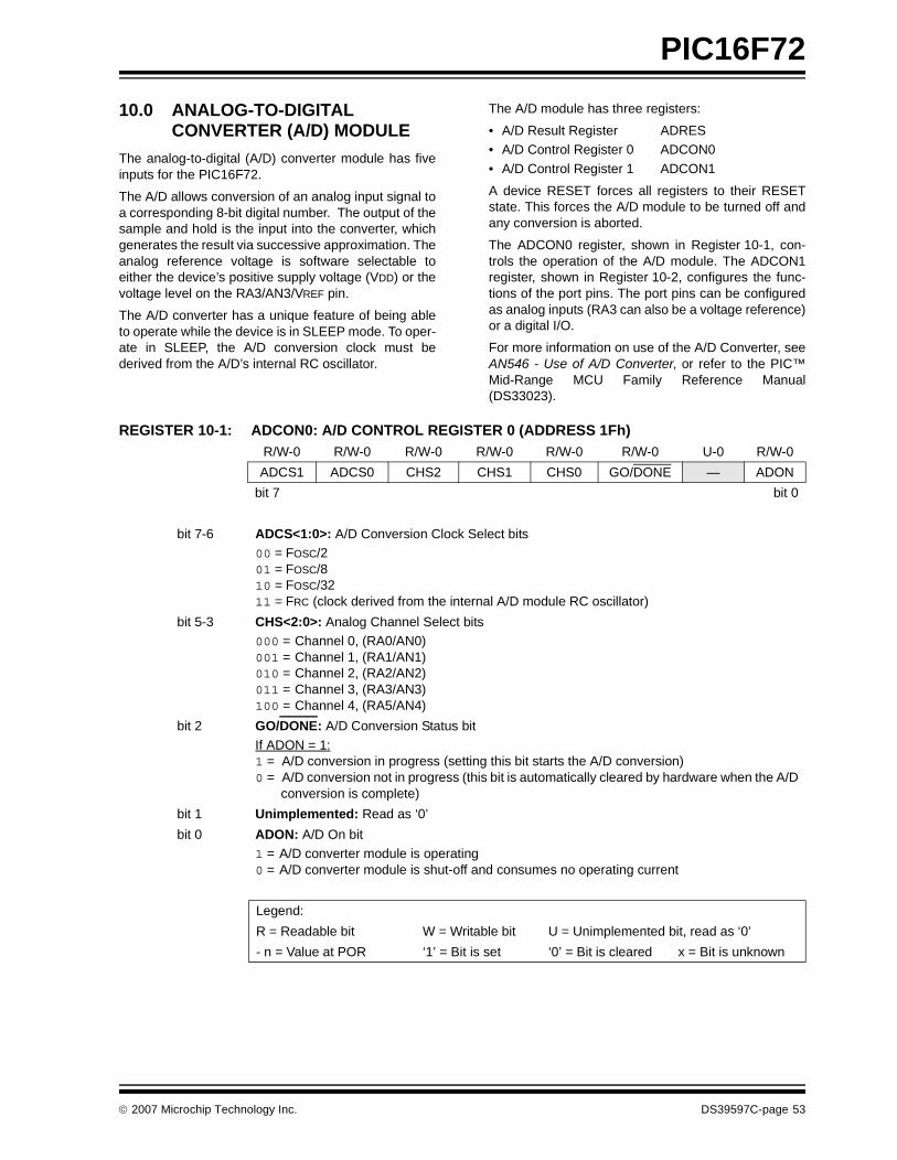
PIC16F72
10.0 ANALOG-TO-DIGITAL CONVERTER (A/D) MODULE
The analog-to-digital (A/D) converter module has fiveinputs for the PIC16F72.
The A/D allows conversion of an analog input signal toa corresponding 8-bit digital number. The output of thesample and hold is the input into the converter, whichgenerates the result via successive approximation. Theanalog reference voltage is software selectable toeither the device’s positive supply voltage (VDD) or thevoltage level on the RA3/AN3/VREF pin.
The A/D converter has a unique feature of being ableto operate while the device is in SLEEP mode. To oper-ate in SLEEP, the A/D conversion clock must bederived from the A/D’s internal RC oscillator.
The A/D module has three registers:
• A/D Result Register ADRES• A/D Control Register 0 ADCON0
• A/D Control Register 1 ADCON1
A device RESET forces all registers to their RESETstate. This forces the A/D module to be turned off andany conversion is aborted.
The ADCON0 register, shown in Register 10-1, con-trols the operation of the A/D module. The ADCON1register, shown in Register 10-2, configures the func-tions of the port pins. The port pins can be configuredas analog inputs (RA3 can also be a voltage reference)or a digital I/O.
For more information on use of the A/D Converter, seeAN546 - Use of A/D Converter, or refer to the PIC™Mid-Range MCU Family Reference Manual(DS33023).
REGISTER 10-1: ADCON0: A/D CONTROL REGISTER 0 (ADDRESS 1Fh) R/W-0 R/W-0 R/W-0 R/W-0 R/W-0 R/W-0 U-0 R/W-0
ADCS1 ADCS0 CHS2 CHS1 CHS0 GO/DONE — ADON
bit 7 bit 0
bit 7-6 ADCS<1:0>: A/D Conversion Clock Select bits00 = FOSC/201 = FOSC/810 = FOSC/3211 = FRC (clock derived from the internal A/D module RC oscillator)
bit 5-3 CHS<2:0>: Analog Channel Select bits000 = Channel 0, (RA0/AN0)001 = Channel 1, (RA1/AN1)010 = Channel 2, (RA2/AN2)011 = Channel 3, (RA3/AN3)100 = Channel 4, (RA5/AN4)
bit 2 GO/DONE: A/D Conversion Status bit
If ADON = 1:1 = A/D conversion in progress (setting this bit starts the A/D conversion)0 = A/D conversion not in progress (this bit is automatically cleared by hardware when the A/D
conversion is complete)
bit 1 Unimplemented: Read as ‘0’
bit 0 ADON: A/D On bit1 = A/D converter module is operating0 = A/D converter module is shut-off and consumes no operating current
Legend:
R = Readable bit W = Writable bit U = Unimplemented bit, read as ‘0’
- n = Value at POR ‘1’ = Bit is set ‘0’ = Bit is cleared x = Bit is unknown
© 2007 Microchip Technology Inc. DS39597C-page 53
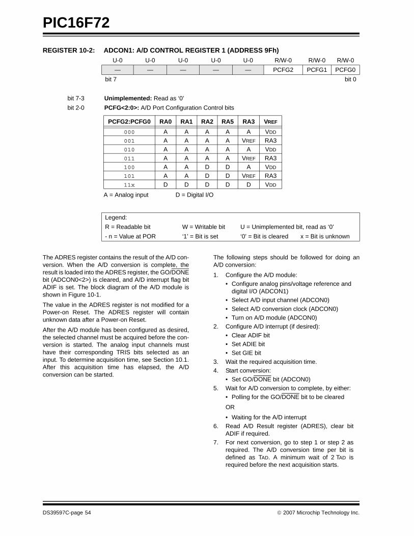
PIC16F72
REGISTER 10-2: ADCON1: A/D CONTROL REGISTER 1 (ADDRESS 9Fh)
The ADRES register contains the result of the A/D con-version. When the A/D conversion is complete, theresult is loaded into the ADRES register, the GO/DONEbit (ADCON0<2>) is cleared, and A/D interrupt flag bitADIF is set. The block diagram of the A/D module isshown in Figure 10-1.
The value in the ADRES register is not modified for aPower-on Reset. The ADRES register will containunknown data after a Power-on Reset.
After the A/D module has been configured as desired,the selected channel must be acquired before the con-version is started. The analog input channels musthave their corresponding TRIS bits selected as aninput. To determine acquisition time, see Section 10.1.After this acquisition time has elapsed, the A/Dconversion can be started.
The following steps should be followed for doing anA/D conversion:
1. Configure the A/D module:• Configure analog pins/voltage reference and
digital I/O (ADCON1)• Select A/D input channel (ADCON0)
• Select A/D conversion clock (ADCON0)• Turn on A/D module (ADCON0)
2. Configure A/D interrupt (if desired):
• Clear ADIF bit • Set ADIE bit • Set GIE bit
3. Wait the required acquisition time.4. Start conversion:
• Set GO/DONE bit (ADCON0)
5. Wait for A/D conversion to complete, by either:• Polling for the GO/DONE bit to be cleared
OR
• Waiting for the A/D interrupt6. Read A/D Result register (ADRES), clear bit
ADIF if required.7. For next conversion, go to step 1 or step 2 as
required. The A/D conversion time per bit isdefined as TAD. A minimum wait of 2 TAD isrequired before the next acquisition starts.
U-0 U-0 U-0 U-0 U-0 R/W-0 R/W-0 R/W-0
— — — — — PCFG2 PCFG1 PCFG0
bit 7 bit 0
bit 7-3 Unimplemented: Read as ‘0’
bit 2-0 PCFG<2:0>: A/D Port Configuration Control bits
Legend:
R = Readable bit W = Writable bit U = Unimplemented bit, read as ‘0’
- n = Value at POR ‘1’ = Bit is set ‘0’ = Bit is cleared x = Bit is unknown
A = Analog input D = Digital I/O
PCFG2:PCFG0 RA0 RA1 RA2 RA5 RA3 VREF
000 A A A A A VDD
001 A A A A VREF RA3010 A A A A A VDD
011 A A A A VREF RA3100 A A D D A VDD
101 A A D D VREF RA3
11x D D D D D VDD
DS39597C-page 54 © 2007 Microchip Technology Inc.

PIC16F72
FIGURE 10-1: A/D BLOCK DIAGRAM
FIGURE 10-2: ANALOG INPUT MODEL
(Input Voltage)
VAIN
VREF
(ReferenceVoltage)
VDD
PCFG2:PCFG0
CHS2:CHS0
000 or010 or100
001 or011 or101
RA5/AN4
RA3/AN3/VREF
RA2/AN2
RA1/AN1
RA0/AN0
100
011
010
001
000
A/DConverter
CPINVA
Rs ANx
5 pF
VDD
VT = 0.6 V
VT = 0.6 VI leakage
RIC ≤ 1 k
SamplingSwitch
SS RSS
CHOLD= DAC capacitance
VSS
6V
Sampling Switch
5V4V3V2V
5 6 7 8 9 10 11
( kΩ )
VDD
= 51.2 pF± 500 nA
Legend: CPIN
VT
I leakage
RIC
SSCHOLD
= input capacitance= threshold voltage= leakage current at the pin due to
= interconnect resistance= sampling switch= sample/hold capacitance (from DAC)
various junctions
© 2007 Microchip Technology Inc. DS39597C-page 55
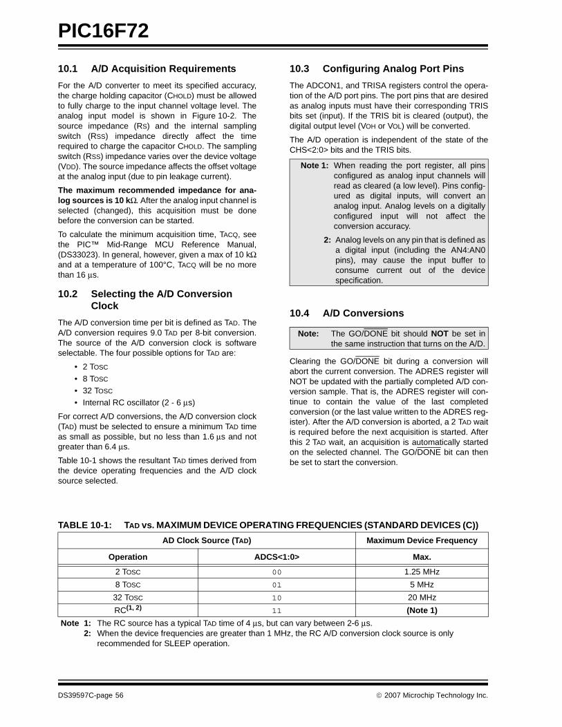
PIC16F72
10.1 A/D Acquisition Requirements
For the A/D converter to meet its specified accuracy,the charge holding capacitor (CHOLD) must be allowedto fully charge to the input channel voltage level. Theanalog input model is shown in Figure 10-2. Thesource impedance (RS) and the internal samplingswitch (RSS) impedance directly affect the timerequired to charge the capacitor CHOLD. The samplingswitch (RSS) impedance varies over the device voltage(VDD). The source impedance affects the offset voltageat the analog input (due to pin leakage current).
The maximum recommended impedance for ana-log sources is 10 kΩ. After the analog input channel isselected (changed), this acquisition must be donebefore the conversion can be started.
To calculate the minimum acquisition time, TACQ, seethe PIC™ Mid-Range MCU Reference Manual,(DS33023). In general, however, given a max of 10 kΩand at a temperature of 100°C, TACQ will be no morethan 16 μs.
10.2 Selecting the A/D Conversion Clock
The A/D conversion time per bit is defined as TAD. TheA/D conversion requires 9.0 TAD per 8-bit conversion.The source of the A/D conversion clock is softwareselectable. The four possible options for TAD are:
• 2 TOSC
• 8 TOSC
• 32 TOSC • Internal RC oscillator (2 - 6 μs)
For correct A/D conversions, the A/D conversion clock(TAD) must be selected to ensure a minimum TAD timeas small as possible, but no less than 1.6 μs and notgreater than 6.4 μs.
Table 10-1 shows the resultant TAD times derived fromthe device operating frequencies and the A/D clocksource selected.
10.3 Configuring Analog Port Pins
The ADCON1, and TRISA registers control the opera-tion of the A/D port pins. The port pins that are desiredas analog inputs must have their corresponding TRISbits set (input). If the TRIS bit is cleared (output), thedigital output level (VOH or VOL) will be converted.
The A/D operation is independent of the state of theCHS<2:0> bits and the TRIS bits.
10.4 A/D Conversions
Clearing the GO/DONE bit during a conversion willabort the current conversion. The ADRES register willNOT be updated with the partially completed A/D con-version sample. That is, the ADRES register will con-tinue to contain the value of the last completedconversion (or the last value written to the ADRES reg-ister). After the A/D conversion is aborted, a 2 TAD waitis required before the next acquisition is started. Afterthis 2 TAD wait, an acquisition is automatically startedon the selected channel. The GO/DONE bit can thenbe set to start the conversion.
TABLE 10-1: TAD vs. MAXIMUM DEVICE OPERATING FREQUENCIES (STANDARD DEVICES (C))
Note 1: When reading the port register, all pinsconfigured as analog input channels willread as cleared (a low level). Pins config-ured as digital inputs, will convert ananalog input. Analog levels on a digitallyconfigured input will not affect theconversion accuracy.
2: Analog levels on any pin that is defined asa digital input (including the AN4:AN0pins), may cause the input buffer toconsume current out of the devicespecification.
Note: The GO/DONE bit should NOT be set inthe same instruction that turns on the A/D.
AD Clock Source (TAD) Maximum Device Frequency
Operation ADCS<1:0> Max.
2 TOSC 00 1.25 MHz
8 TOSC 01 5 MHz
32 TOSC 10 20 MHz
RC(1, 2) 11 (Note 1)
Note 1: The RC source has a typical TAD time of 4 μs, but can vary between 2-6 μs.2: When the device frequencies are greater than 1 MHz, the RC A/D conversion clock source is only
recommended for SLEEP operation.
DS39597C-page 56 © 2007 Microchip Technology Inc.
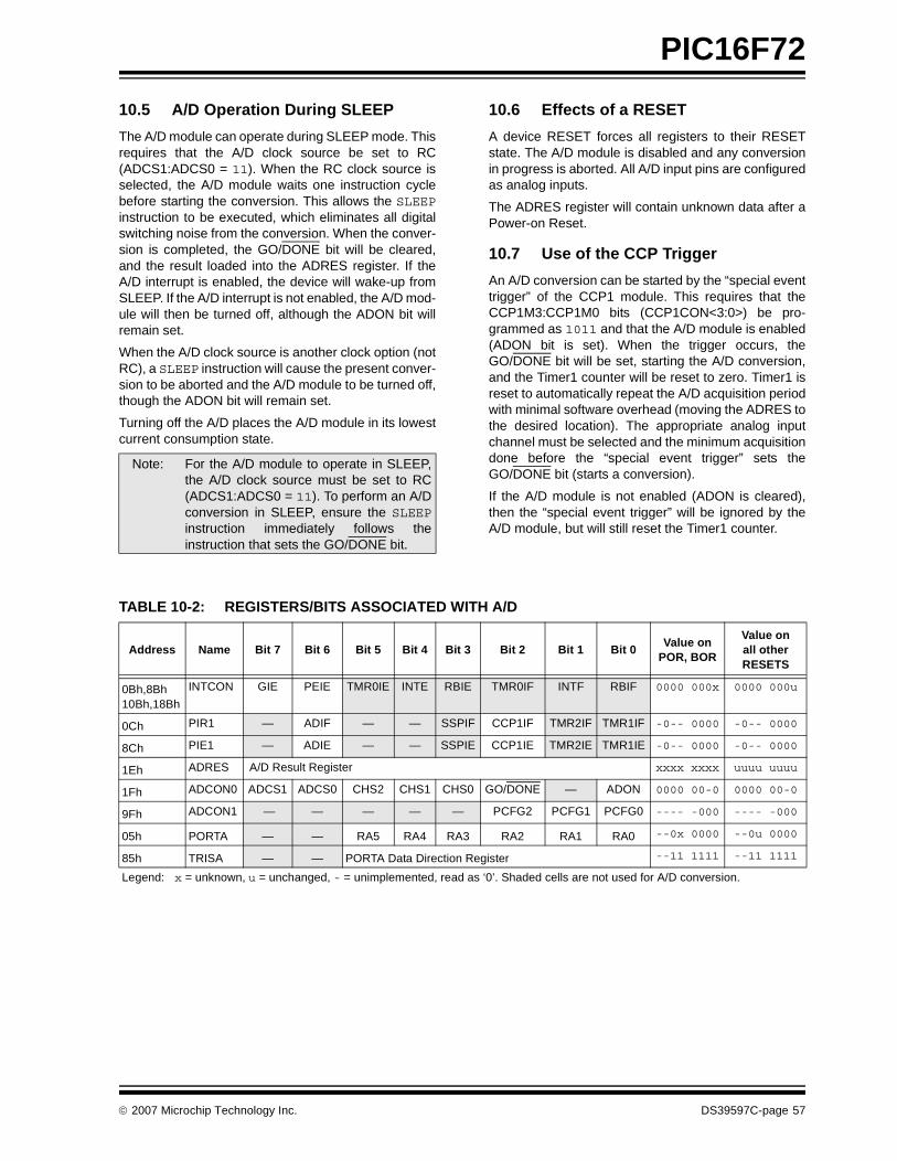
PIC16F72
10.5 A/D Operation During SLEEP
The A/D module can operate during SLEEP mode. Thisrequires that the A/D clock source be set to RC(ADCS1:ADCS0 = 11). When the RC clock source isselected, the A/D module waits one instruction cyclebefore starting the conversion. This allows the SLEEPinstruction to be executed, which eliminates all digitalswitching noise from the conversion. When the conver-sion is completed, the GO/DONE bit will be cleared,and the result loaded into the ADRES register. If theA/D interrupt is enabled, the device will wake-up fromSLEEP. If the A/D interrupt is not enabled, the A/D mod-ule will then be turned off, although the ADON bit willremain set.
When the A/D clock source is another clock option (notRC), a SLEEP instruction will cause the present conver-sion to be aborted and the A/D module to be turned off,though the ADON bit will remain set.
Turning off the A/D places the A/D module in its lowestcurrent consumption state.
10.6 Effects of a RESET
A device RESET forces all registers to their RESETstate. The A/D module is disabled and any conversionin progress is aborted. All A/D input pins are configuredas analog inputs.
The ADRES register will contain unknown data after aPower-on Reset.
10.7 Use of the CCP Trigger
An A/D conversion can be started by the “special eventtrigger” of the CCP1 module. This requires that theCCP1M3:CCP1M0 bits (CCP1CON<3:0>) be pro-grammed as 1011 and that the A/D module is enabled(ADON bit is set). When the trigger occurs, theGO/DONE bit will be set, starting the A/D conversion,and the Timer1 counter will be reset to zero. Timer1 isreset to automatically repeat the A/D acquisition periodwith minimal software overhead (moving the ADRES tothe desired location). The appropriate analog inputchannel must be selected and the minimum acquisitiondone before the “special event trigger” sets theGO/DONE bit (starts a conversion).
If the A/D module is not enabled (ADON is cleared),then the “special event trigger” will be ignored by theA/D module, but will still reset the Timer1 counter.
TABLE 10-2: REGISTERS/BITS ASSOCIATED WITH A/D
Note: For the A/D module to operate in SLEEP,the A/D clock source must be set to RC(ADCS1:ADCS0 = 11). To perform an A/Dconversion in SLEEP, ensure the SLEEPinstruction immediately follows theinstruction that sets the GO/DONE bit.
Address Name Bit 7 Bit 6 Bit 5 Bit 4 Bit 3 Bit 2 Bit 1 Bit 0Value on
POR, BOR
Value on all other RESETS
0Bh,8Bh10Bh,18Bh
INTCON GIE PEIE TMR0IE INTE RBIE TMR0IF INTF RBIF 0000 000x 0000 000u
0Ch PIR1 — ADIF — — SSPIF CCP1IF TMR2IF TMR1IF -0-- 0000 -0-- 0000
8Ch PIE1 — ADIE — — SSPIE CCP1IE TMR2IE TMR1IE -0-- 0000 -0-- 0000
1Eh ADRES A/D Result Register xxxx xxxx uuuu uuuu
1Fh ADCON0 ADCS1 ADCS0 CHS2 CHS1 CHS0 GO/DONE — ADON 0000 00-0 0000 00-0
9Fh ADCON1 — — — — — PCFG2 PCFG1 PCFG0 ---- -000 ---- -000
05h PORTA — — RA5 RA4 RA3 RA2 RA1 RA0 --0x 0000 --0u 0000
85h TRISA — — PORTA Data Direction Register --11 1111 --11 1111
Legend: x = unknown, u = unchanged, - = unimplemented, read as ‘0’. Shaded cells are not used for A/D conversion.
© 2007 Microchip Technology Inc. DS39597C-page 57

PIC16F72
NOTES:
DS39597C-page 58 © 2007 Microchip Technology Inc.
PIC16F72
11.0 SPECIAL FEATURES OF THE CPU
These devices have a host of features intended to max-imize system reliability, minimize cost through elimina-tion of external components, provide power savingOperating modes and offer code protection:
• Oscillator Selection
• RESET- Power-on Reset (POR)- Power-up Timer (PWRT)
- Oscillator Start-up Timer (OST)- Brown-out Reset (BOR)
• Interrupts
• Watchdog Timer (WDT)• SLEEP• Code Protection
• ID Locations• In-Circuit Serial Programming
These devices have a Watchdog Timer, which can beenabled or disabled using a configuration bit. It runs offits own RC oscillator for added reliability.
There are two timers that offer necessary delays onpower-up. One is the Oscillator Start-up Timer (OST),intended to keep the chip in RESET until the crystaloscillator is stable. The other is the Power-up Timer(PWRT), which provides a fixed delay of 72 ms (nomi-nal) on power-up only. It is designed to keep the part inRESET while the power supply stabilizes, and isenabled or disabled using a configuration bit. Withthese two timers on-chip, most applications need noexternal RESET circuitry.
SLEEP mode is designed to offer a very low currentPower-down mode. The user can wake-up fromSLEEP through external RESET, Watchdog TimerWake-up, or through an interrupt.
Several oscillator options are also made available toallow the part to fit the application. The RC oscillatoroption saves system cost while the LP crystal optionsaves power. Configuration bits are used to select thedesired oscillator mode.
Additional information on special features is availablein the PIC™ Mid-Range Reference Manual (DS33023).
11.1 Configuration Bits
The configuration bits can be programmed (read as‘0’), or left unprogrammed (read as ‘1’), to select vari-ous device configurations. These bits are mapped inprogram memory location 2007h.
The user will note that address 2007h is beyond theuser program memory space, which can be accessedonly during programming.
© 2007 Microchip Technology Inc. DS39597C-page 59
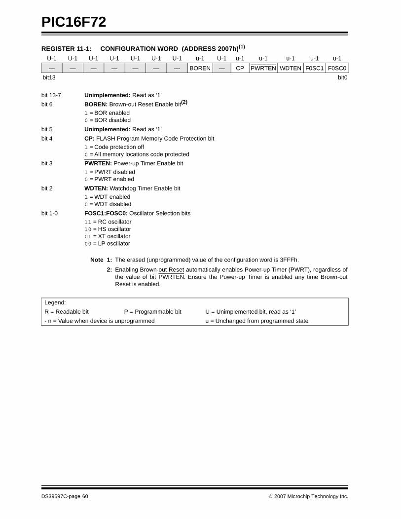
PIC16F72
REGISTER 11-1: CONFIGURATION WORD (ADDRESS 2007h)(1)
U-1 U-1 U-1 U-1 U-1 U-1 U-1 u-1 U-1 u-1 u-1 u-1 u-1 u-1
— — — — — — — BOREN — CP PWRTEN WDTEN F0SC1 F0SC0
bit13 bit0
bit 13-7 Unimplemented: Read as ‘1’
bit 6 BOREN: Brown-out Reset Enable bit(2)
1 = BOR enabled0 = BOR disabled
bit 5 Unimplemented: Read as ‘1’
bit 4 CP: FLASH Program Memory Code Protection bit1 = Code protection off 0 = All memory locations code protected
bit 3 PWRTEN: Power-up Timer Enable bit
1 = PWRT disabled0 = PWRT enabled
bit 2 WDTEN: Watchdog Timer Enable bit1 = WDT enabled0 = WDT disabled
bit 1-0 FOSC1:FOSC0: Oscillator Selection bits11 = RC oscillator10 = HS oscillator01 = XT oscillator00 = LP oscillator
Note 1: The erased (unprogrammed) value of the configuration word is 3FFFh.
2: Enabling Brown-out Reset automatically enables Power-up Timer (PWRT), regardless ofthe value of bit PWRTEN. Ensure the Power-up Timer is enabled any time Brown-outReset is enabled.
Legend:
R = Readable bit P = Programmable bit U = Unimplemented bit, read as ‘1’
- n = Value when device is unprogrammed u = Unchanged from programmed state
DS39597C-page 60 © 2007 Microchip Technology Inc.
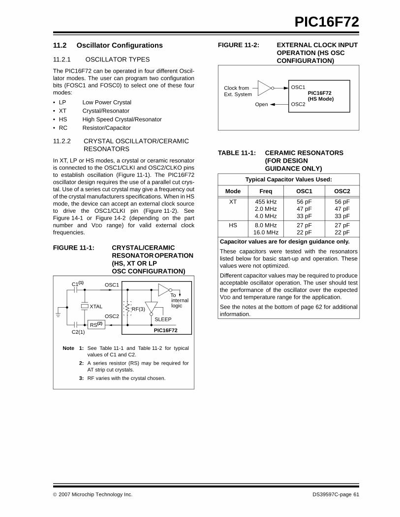
PIC16F72
11.2 Oscillator Configurations11.2.1 OSCILLATOR TYPES
The PIC16F72 can be operated in four different Oscil-lator modes. The user can program two configurationbits (FOSC1 and FOSC0) to select one of these fourmodes:
• LP Low Power Crystal• XT Crystal/Resonator
• HS High Speed Crystal/Resonator• RC Resistor/Capacitor
11.2.2 CRYSTAL OSCILLATOR/CERAMIC RESONATORS
In XT, LP or HS modes, a crystal or ceramic resonatoris connected to the OSC1/CLKI and OSC2/CLKO pinsto establish oscillation (Figure 11-1). The PIC16F72oscillator design requires the use of a parallel cut crys-tal. Use of a series cut crystal may give a frequency outof the crystal manufacturers specifications. When in HSmode, the device can accept an external clock sourceto drive the OSC1/CLKI pin (Figure 11-2). SeeFigure 14-1 or Figure 14-2 (depending on the partnumber and VDD range) for valid external clockfrequencies.
FIGURE 11-1: CRYSTAL/CERAMIC RESONATOR OPERATION (HS, XT OR LP OSC CONFIGURATION)
FIGURE 11-2: EXTERNAL CLOCK INPUT OPERATION (HS OSC CONFIGURATION)
TABLE 11-1: CERAMIC RESONATORS (FOR DESIGN GUIDANCE ONLY)
Note 1: See Table 11-1 and Table 11-2 for typicalvalues of C1 and C2.
2: A series resistor (RS) may be required forAT strip cut crystals.
3: RF varies with the crystal chosen.
C1(1)
C2(1)
XTAL
OSC2
OSC1
RF(3)
SLEEP
To
logic
PIC16F72RS(2)
internal
Typical Capacitor Values Used:
Mode Freq OSC1 OSC2
XT 455 kHz2.0 MHz4.0 MHz
56 pF47 pF33 pF
56 pF47 pF33 pF
HS 8.0 MHz16.0 MHz
27 pF22 pF
27 pF22 pF
Capacitor values are for design guidance only.
These capacitors were tested with the resonatorslisted below for basic start-up and operation. Thesevalues were not optimized.
Different capacitor values may be required to produceacceptable oscillator operation. The user should testthe performance of the oscillator over the expectedVDD and temperature range for the application.
See the notes at the bottom of page 62 for additionalinformation.
OSC1
OSC2Open
Clock fromExt. System PIC16F72
(HS Mode)
© 2007 Microchip Technology Inc. DS39597C-page 61
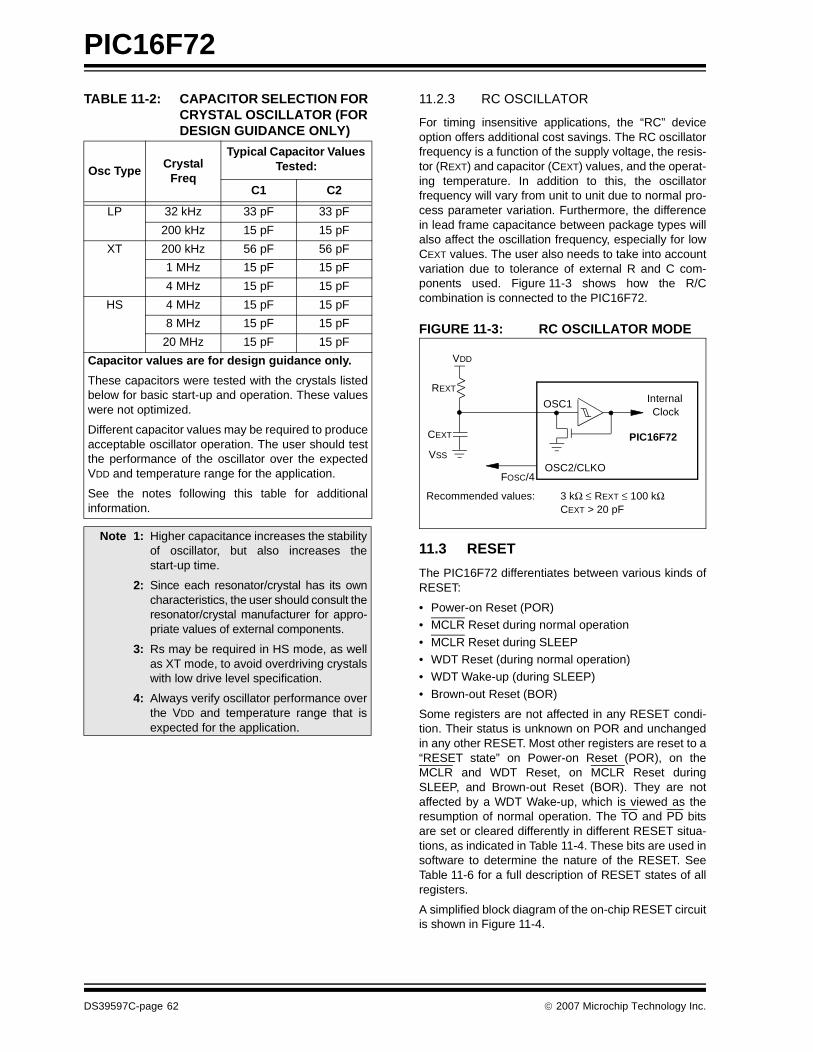
PIC16F72
TABLE 11-2: CAPACITOR SELECTION FOR CRYSTAL OSCILLATOR (FOR DESIGN GUIDANCE ONLY)
11.2.3 RC OSCILLATOR
For timing insensitive applications, the “RC” deviceoption offers additional cost savings. The RC oscillatorfrequency is a function of the supply voltage, the resis-tor (REXT) and capacitor (CEXT) values, and the operat-ing temperature. In addition to this, the oscillatorfrequency will vary from unit to unit due to normal pro-cess parameter variation. Furthermore, the differencein lead frame capacitance between package types willalso affect the oscillation frequency, especially for lowCEXT values. The user also needs to take into accountvariation due to tolerance of external R and C com-ponents used. Figure 11-3 shows how the R/Ccombination is connected to the PIC16F72.
FIGURE 11-3: RC OSCILLATOR MODE
11.3 RESET
The PIC16F72 differentiates between various kinds ofRESET:
• Power-on Reset (POR)• MCLR Reset during normal operation
• MCLR Reset during SLEEP• WDT Reset (during normal operation)• WDT Wake-up (during SLEEP)
• Brown-out Reset (BOR)
Some registers are not affected in any RESET condi-tion. Their status is unknown on POR and unchangedin any other RESET. Most other registers are reset to a“RESET state” on Power-on Reset (POR), on theMCLR and WDT Reset, on MCLR Reset duringSLEEP, and Brown-out Reset (BOR). They are notaffected by a WDT Wake-up, which is viewed as theresumption of normal operation. The TO and PD bitsare set or cleared differently in different RESET situa-tions, as indicated in Table 11-4. These bits are used insoftware to determine the nature of the RESET. SeeTable 11-6 for a full description of RESET states of allregisters.
A simplified block diagram of the on-chip RESET circuitis shown in Figure 11-4.
Osc TypeCrystal
Freq
Typical Capacitor Values Tested:
C1 C2
LP 32 kHz 33 pF 33 pF
200 kHz 15 pF 15 pF
XT 200 kHz 56 pF 56 pF
1 MHz 15 pF 15 pF
4 MHz 15 pF 15 pF
HS 4 MHz 15 pF 15 pF
8 MHz 15 pF 15 pF
20 MHz 15 pF 15 pF
Capacitor values are for design guidance only.
These capacitors were tested with the crystals listedbelow for basic start-up and operation. These valueswere not optimized.
Different capacitor values may be required to produceacceptable oscillator operation. The user should testthe performance of the oscillator over the expectedVDD and temperature range for the application.
See the notes following this table for additionalinformation.
Note 1: Higher capacitance increases the stabilityof oscillator, but also increases thestart-up time.
2: Since each resonator/crystal has its owncharacteristics, the user should consult theresonator/crystal manufacturer for appro-priate values of external components.
3: Rs may be required in HS mode, as wellas XT mode, to avoid overdriving crystalswith low drive level specification.
4: Always verify oscillator performance overthe VDD and temperature range that isexpected for the application.
OSC2/CLKO
CEXT
REXT
PIC16F72
OSC1
FOSC/4
InternalClock
VDD
VSS
Recommended values: 3 kΩ ≤ REXT ≤ 100 kΩCEXT > 20 pF
DS39597C-page 62 © 2007 Microchip Technology Inc.
PIC16F72
FIGURE 11-4: SIMPLIFIED BLOCK DIAGRAM OF ON-CHIP RESET CIRCUIT
11.4 MCLR
PIC16F72 device has a noise filter in the MCLR Resetpath. The filter will detect and ignore small pulses.
It should be noted that a WDT Reset does not driveMCLR pin low.
The behavior of the ESD protection on the MCLR pinhas been altered from previous devices of this family.Voltages applied to the pin that exceed its specificationcan result in both MCLR and excessive current beyondthe device specification during the ESD event. For thisreason, Microchip recommends that the MCLR pin nolonger be tied directly to VDD. The use of anRC network, as shown in Figure 11-5, is suggested.
FIGURE 11-5: RECOMMENDED MCLR CIRCUIT
S
R Q
ExternalRESET
MCLR
VDD
OSC1
WDTModule
VDD RiseDetect
OST/PWRT
On-chip RC OSC
WDT
Time-out
Power-on Reset
OST
10-bit Ripple Counter
PWRT
Chip_Reset
10-bit Ripple Counter
Reset
Enable OST
Enable PWRT
SLEEP
Note 1: This is a separate oscillator from the RC oscillator of the CLKI pin.
Brown-outReset BOREN
(1)
C10.1 μF
R11 kΩ (or greater)
(optional, not critical)
VDD
MCLR
PIC16F72
© 2007 Microchip Technology Inc. DS39597C-page 63
PIC16F72
11.5 Power-on Reset (POR)
A Power-on Reset pulse is generated on-chip whenVDD rise is detected (in the range of 1.2V - 1.7V). Totake advantage of the POR, tie the MCLR pin to VDD,as described in Section 11.4. A maximum rise time forVDD is specified. See Section 14.0, ElectricalCharacteristics for details.
When the device starts normal operation (exits theRESET condition), device operating parameters (volt-age, frequency, temperature,...) must be met to ensureoperation. If these conditions are not met, the devicemust be held in RESET until the operating conditionsare met. For more information, see Application Note,AN607- Power-up Trouble Shooting (DS00607).
11.6 Power-up Timer (PWRT)
The Power-up Timer provides a fixed 72 ms nominaltime-out on power-up only from the POR. The Power-up Timer operates on an internal RC oscillator. Thechip is kept in RESET as long as the PWRT is active.The PWRT’s time delay allows VDD to rise to an accept-able level. A configuration bit is provided to enable/disable the PWRT.
The power-up time delay will vary from chip to chip dueto VDD, temperature and process variation. See DCparameters for details (TPWRT, parameter #33).
11.7 Oscillator Start-up Timer (OST)
The Oscillator Start-up Timer (OST) provides 1024oscillator cycles (from OSC1 input) delay after thePWRT delay is over (if enabled). This helps to ensurethat the crystal oscillator or resonator has started andstabilized.
The OST time-out is invoked only for XT, LP and HSmodes and only on Power-on Reset or wake-up fromSLEEP.
11.8 Brown-out Reset (BOR)
The configuration bit, BOREN, can enable or disablethe Brown-out Reset circuit. If VDD falls below VBOR
(parameter D005, about 4V) for longer than TBOR
(parameter #35, about 100 μs), the brown-out situationwill reset the device. If VDD falls below VBOR for lessthan TBOR, a RESET may not occur.
Once the brown-out occurs, the device will remain inBrown-out Reset until VDD rises above VBOR. ThePower-up Timer then keeps the device in RESET forTPWRT (parameter #33, about 72 ms). If VDD should fallbelow VBOR during TPWRT, the Brown-out Reset pro-cess will restart when VDD rises above VBOR, with thePower-up Timer Reset. The Power-up Timer is alwaysenabled when the Brown-out Reset circuit is enabled,regardless of the state of the PWRT configuration bit.
11.9 Time-out Sequence
On power-up, the time-out sequence is as follows: thePWRT delay starts (if enabled) when a POR occurs.Then, OST starts counting 1024 oscillator cycles whenPWRT ends (LP, XT, HS). When the OST ends, thedevice comes out of RESET.
If MCLR is kept low long enough, all delays will expire.Bringing MCLR high will begin execution immediately.This is useful for testing purposes or to synchronizemore than one PIC16F72 device operating in parallel.
Table 11-5 shows the RESET conditions for theSTATUS, PCON and PC registers, while Table 11-6shows the RESET conditions for all the registers.
11.10 Power Control/Status Register (PCON)
The Power Control/Status Register, PCON, has twobits to indicate the type of RESET that last occurred.
Bit0 is Brown-out Reset Status bit, BOR. Bit BOR isunknown on a Power-on Reset. It must then be set bythe user and checked on subsequent RESETS to seeif bit BOR cleared, indicating a Brown-out Resetoccurred. When the Brown-out Reset is disabled, thestate of the BOR bit is unpredictable.
Bit1 is POR (Power-on Reset Status bit). It is cleared ona Power-on Reset and unaffected otherwise. The usermust set this bit following a Power-on Reset.
DS39597C-page 64 © 2007 Microchip Technology Inc.

PIC16F72
TABLE 11-3: TIME-OUT IN VARIOUS SITUATIONS
TABLE 11-4: STATUS BITS AND THEIR SIGNIFICANCE
TABLE 11-5: RESET CONDITION FOR SPECIAL REGISTERS
Oscillator ConfigurationPower-up
Brown-outWake-up from
SLEEPPWRTEN = 0 PWRTEN = 1
XT, HS, LP 72 ms + 1024 TOSC 1024 TOSC 72 ms + 1024 TOSC 1024 TOSC
RC 72 ms — 72 ms —
POR(PCON<1>)
BOR(PCON<0>)
TO(STATUS<4>)
PD(STATUS<3>)
Significance
0 x 1 1 Power-on Reset
0 x 0 x Illegal, TO is set on POR
0 x x 0 Illegal, PD is set on POR
u 0 1 1 Brown-out Reset
u u 0 1 WDT Reset
u u 0 0 WDT Wake-up
u u u u MCLR Reset during normal operation
u u 1 0 MCLR Reset during SLEEP or interrupt wake-up from SLEEP
ConditionProgramCounter
STATUSRegister
PCONRegister
Power-on Reset 000h 0001 1xxx ---- --0x
MCLR Reset during normal operation 000h 000u uuuu ---- --uu
MCLR Reset during SLEEP 000h 0001 0uuu ---- --uu
WDT Reset 000h 0000 1uuu ---- --uu
WDT Wake-up PC + 1 uuu0 0uuu ---- --uu
Brown-out Reset 000h 0001 1uuu ---- --u0
Interrupt Wake-up from SLEEP PC + 1(1) uuu1 0uuu ---- --uu
Legend: u = unchanged, x = unknown, - = unimplemented bit, read as '0'.Note 1: When the wake-up is due to an interrupt and the GIE bit is set, the PC is loaded with the interrupt vector
(0004h).
© 2007 Microchip Technology Inc. DS39597C-page 65
PIC16F72
TABLE 11-6: INITIALIZATION CONDITIONS FOR ALL REGISTERS
RegisterPower-on Reset,Brown-out Reset
MCLR Reset,WDT Reset
Wake-up via WDT or Interrupt
W xxxx xxxx uuuu uuuu uuuu uuuu
INDF N/A N/A N/A
TMR0 xxxx xxxx uuuu uuuu uuuu uuuu
PCL 0000h 0000h PC + 1(2)
STATUS 0001 1xxx 000q quuu(3) uuuq quuu(3)
FSR xxxx xxxx uuuu uuuu uuuu uuuu
PORTA --0x 0000 --0u 0000 --uu uuuu
PORTB xxxx xxxx uuuu uuuu uuuu uuuu
PORTC xxxx xxxx uuuu uuuu uuuu uuuu
PCLATH ---0 0000 ---0 0000 ---u uuuu
INTCON 0000 000x 0000 000u uuuu uuuu(1)
PIR1 -0-- 0000 -0-- 0000 -u-- uuuu(1)
TMR1L xxxx xxxx uuuu uuuu uuuu uuuu
TMR1H xxxx xxxx uuuu uuuu uuuu uuuu
T1CON --00 0000 --uu uuuu --uu uuuu
TMR2 0000 0000 0000 0000 uuuu uuuu
T2CON -000 0000 -000 0000 -uuu uuuu
SSPBUF xxxx xxxx uuuu uuuu uuuu uuuu
SSPCON 0000 0000 0000 0000 uuuu uuuu
CCPR1L xxxx xxxx uuuu uuuu uuuu uuuu
CCPR1H xxxx xxxx uuuu uuuu uuuu uuuu
CCP1CON --00 0000 --00 0000 --uu uuuu
ADRES xxxx xxxx uuuu uuuu uuuu uuuu
ADCON0 0000 00-0 0000 00-0 uuuu uu-u
OPTION 1111 1111 1111 1111 uuuu uuuu
TRISA --11 1111 --11 1111 --uu uuuu
TRISB 1111 1111 1111 1111 uuuu uuuu
TRISC 1111 1111 1111 1111 uuuu uuuu
PIE1 -0-- 0000 -0-- 0000 -u-- uuuu
PCON ---- --qq ---- --uu ---- --uu
PR2 1111 1111 1111 1111 1111 1111
SSPADD 0000 0000 0000 0000 uuuu uuuu
SSPSTAT --00 0000 --00 0000 --uu uuuu
ADCON1 ---- -000 ---- -000 ---- -uuu
PMDATL 0--- 0000 0--- 0000 u--- uuuu
PMADRL xxxx xxxx uuuu uuuu uuuu uuuu
PMDATH xxxx xxxx uuuu uuuu uuuu uuuu
PMADRH xxxx xxxx uuuu uuuu uuuu uuuu
PMCON1 1--- ---0 1--- ---0 1--- ---u
Legend: u = unchanged, x = unknown, - = unimplemented bit, read as '0', q = value depends on condition, r = reserved, maintain clear.
Note 1: One or more bits in INTCON, PIR1 will be affected (to cause wake-up).2: When the wake-up is due to an interrupt and the GIE bit is set, the PC is loaded with the interrupt vector
(0004h).3: See Table 11-5 for RESET value for specific condition.
DS39597C-page 66 © 2007 Microchip Technology Inc.
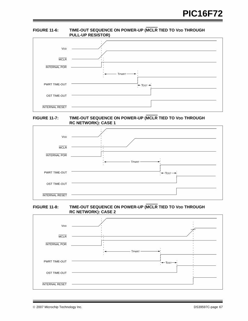
PIC16F72
FIGURE 11-6: TIME-OUT SEQUENCE ON POWER-UP (MCLR TIED TO VDD THROUGH PULL-UP RESISTOR)
FIGURE 11-7: TIME-OUT SEQUENCE ON POWER-UP (MCLR TIED TO VDD THROUGHRC NETWORK): CASE 1
FIGURE 11-8: TIME-OUT SEQUENCE ON POWER-UP (MCLR TIED TO VDD THROUGHRC NETWORK): CASE 2
TPWRT
TOST
VDD
MCLR
INTERNAL POR
PWRT TIME-OUT
OST TIME-OUT
INTERNAL RESET
TPWRT
TOST
VDD
MCLR
INTERNAL POR
PWRT TIME-OUT
OST TIME-OUT
INTERNAL RESET
VDD
MCLR
INTERNAL POR
PWRT TIME-OUT
OST TIME-OUT
INTERNAL RESET
TPWRT
TOST
© 2007 Microchip Technology Inc. DS39597C-page 67
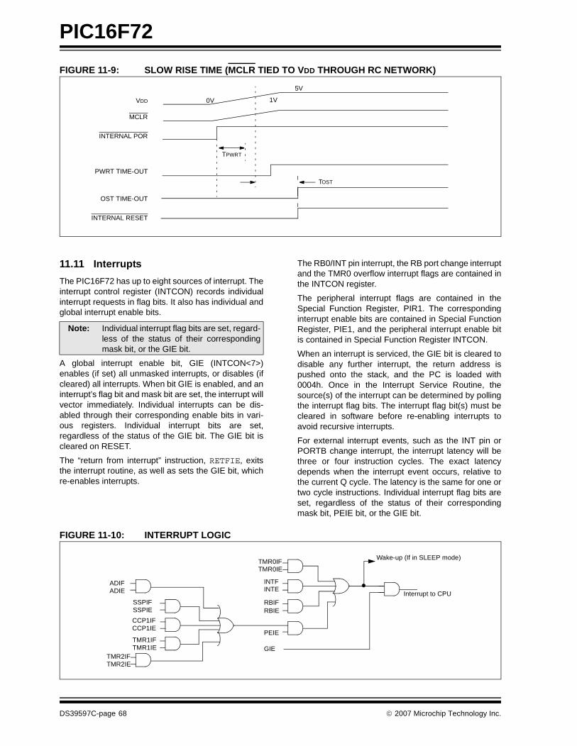
PIC16F72
FIGURE 11-9: SLOW RISE TIME (MCLR TIED TO VDD THROUGH RC NETWORK)
11.11 Interrupts
The PIC16F72 has up to eight sources of interrupt. Theinterrupt control register (INTCON) records individualinterrupt requests in flag bits. It also has individual andglobal interrupt enable bits.
A global interrupt enable bit, GIE (INTCON<7>)enables (if set) all unmasked interrupts, or disables (ifcleared) all interrupts. When bit GIE is enabled, and aninterrupt’s flag bit and mask bit are set, the interrupt willvector immediately. Individual interrupts can be dis-abled through their corresponding enable bits in vari-ous registers. Individual interrupt bits are set,regardless of the status of the GIE bit. The GIE bit iscleared on RESET.
The “return from interrupt” instruction, RETFIE, exitsthe interrupt routine, as well as sets the GIE bit, whichre-enables interrupts.
The RB0/INT pin interrupt, the RB port change interruptand the TMR0 overflow interrupt flags are contained inthe INTCON register.
The peripheral interrupt flags are contained in theSpecial Function Register, PIR1. The correspondinginterrupt enable bits are contained in Special FunctionRegister, PIE1, and the peripheral interrupt enable bitis contained in Special Function Register INTCON.
When an interrupt is serviced, the GIE bit is cleared todisable any further interrupt, the return address ispushed onto the stack, and the PC is loaded with0004h. Once in the Interrupt Service Routine, thesource(s) of the interrupt can be determined by pollingthe interrupt flag bits. The interrupt flag bit(s) must becleared in software before re-enabling interrupts toavoid recursive interrupts.
For external interrupt events, such as the INT pin orPORTB change interrupt, the interrupt latency will bethree or four instruction cycles. The exact latencydepends when the interrupt event occurs, relative tothe current Q cycle. The latency is the same for one ortwo cycle instructions. Individual interrupt flag bits areset, regardless of the status of their correspondingmask bit, PEIE bit, or the GIE bit.
FIGURE 11-10: INTERRUPT LOGIC
VDD
MCLR
INTERNAL POR
PWRT TIME-OUT
OST TIME-OUT
INTERNAL RESET
0V 1V
5V
TPWRT
TOST
Note: Individual interrupt flag bits are set, regard-less of the status of their correspondingmask bit, or the GIE bit.
ADIFADIE
SSPIFSSPIE
CCP1IFCCP1IE
TMR2IFTMR2IE
TMR1IFTMR1IE
TMR0IFTMR0IE
INTFINTE
RBIFRBIE
GIE
PEIE
Wake-up (If in SLEEP mode)
Interrupt to CPU
DS39597C-page 68 © 2007 Microchip Technology Inc.
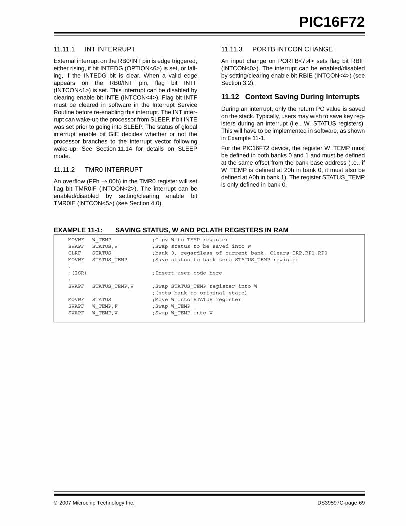
PIC16F72
11.11.1 INT INTERRUPT
External interrupt on the RB0/INT pin is edge triggered,either rising, if bit INTEDG (OPTION<6>) is set, or fall-ing, if the INTEDG bit is clear. When a valid edgeappears on the RB0/INT pin, flag bit INTF(INTCON<1>) is set. This interrupt can be disabled byclearing enable bit INTE (INTCON<4>). Flag bit INTFmust be cleared in software in the Interrupt ServiceRoutine before re-enabling this interrupt. The INT inter-rupt can wake-up the processor from SLEEP, if bit INTEwas set prior to going into SLEEP. The status of globalinterrupt enable bit GIE decides whether or not theprocessor branches to the interrupt vector followingwake-up. See Section 11.14 for details on SLEEPmode.
11.11.2 TMR0 INTERRUPT
An overflow (FFh → 00h) in the TMR0 register will setflag bit TMR0IF (INTCON<2>). The interrupt can beenabled/disabled by setting/clearing enable bitTMR0IE (INTCON<5>) (see Section 4.0).
11.11.3 PORTB INTCON CHANGE
An input change on PORTB<7:4> sets flag bit RBIF(INTCON<0>). The interrupt can be enabled/disabledby setting/clearing enable bit RBIE (INTCON<4>) (seeSection 3.2).
11.12 Context Saving During Interrupts
During an interrupt, only the return PC value is savedon the stack. Typically, users may wish to save key reg-isters during an interrupt (i.e., W, STATUS registers).This will have to be implemented in software, as shownin Example 11-1.
For the PIC16F72 device, the register W_TEMP mustbe defined in both banks 0 and 1 and must be definedat the same offset from the bank base address (i.e., ifW_TEMP is defined at 20h in bank 0, it must also bedefined at A0h in bank 1). The register STATUS_TEMPis only defined in bank 0.
EXAMPLE 11-1: SAVING STATUS, W AND PCLATH REGISTERS IN RAM MOVWF W_TEMP ;Copy W to TEMP registerSWAPF STATUS,W ;Swap status to be saved into W CLRF STATUS ;bank 0, regardless of current bank, Clears IRP,RP1,RP0MOVWF STATUS_TEMP ;Save status to bank zero STATUS_TEMP register::(ISR) ;Insert user code here:SWAPF STATUS_TEMP,W ;Swap STATUS_TEMP register into W
;(sets bank to original state)MOVWF STATUS ;Move W into STATUS registerSWAPF W_TEMP,F ;Swap W_TEMPSWAPF W_TEMP,W ;Swap W_TEMP into W
© 2007 Microchip Technology Inc. DS39597C-page 69
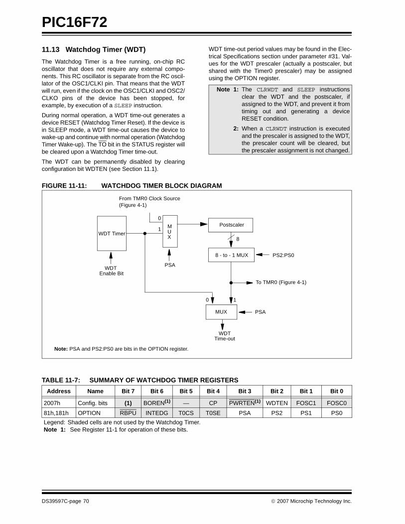
PIC16F72
11.13 Watchdog Timer (WDT)
The Watchdog Timer is a free running, on-chip RCoscillator that does not require any external compo-nents. This RC oscillator is separate from the RC oscil-lator of the OSC1/CLKI pin. That means that the WDTwill run, even if the clock on the OSC1/CLKI and OSC2/CLKO pins of the device has been stopped, forexample, by execution of a SLEEP instruction.
During normal operation, a WDT time-out generates adevice RESET (Watchdog Timer Reset). If the device isin SLEEP mode, a WDT time-out causes the device towake-up and continue with normal operation (WatchdogTimer Wake-up). The TO bit in the STATUS register willbe cleared upon a Watchdog Timer time-out.
The WDT can be permanently disabled by clearingconfiguration bit WDTEN (see Section 11.1).
WDT time-out period values may be found in the Elec-trical Specifications section under parameter #31. Val-ues for the WDT prescaler (actually a postscaler, butshared with the Timer0 prescaler) may be assignedusing the OPTION register.
FIGURE 11-11: WATCHDOG TIMER BLOCK DIAGRAM
TABLE 11-7: SUMMARY OF WATCHDOG TIMER REGISTERS
Note 1: The CLRWDT and SLEEP instructionsclear the WDT and the postscaler, ifassigned to the WDT, and prevent it fromtiming out and generating a deviceRESET condition.
2: When a CLRWDT instruction is executedand the prescaler is assigned to the WDT,the prescaler count will be cleared, butthe prescaler assignment is not changed.
From TMR0 Clock Source(Figure 4-1)
To TMR0 (Figure 4-1)
Postscaler
WDT Timer
WDT Enable Bit
0
1 MUX
PSA
8 - to - 1 MUX PS2:PS0
0 1
MUX PSA
WDTTime-out
Note: PSA and PS2:PS0 are bits in the OPTION register.
8
Address Name Bit 7 Bit 6 Bit 5 Bit 4 Bit 3 Bit 2 Bit 1 Bit 0
2007h Config. bits (1) BOREN(1) — CP PWRTEN(1) WDTEN FOSC1 FOSC0
81h,181h OPTION RBPU INTEDG T0CS T0SE PSA PS2 PS1 PS0
Legend: Shaded cells are not used by the Watchdog Timer.Note 1: See Register 11-1 for operation of these bits.
DS39597C-page 70 © 2007 Microchip Technology Inc.
PIC16F72
11.14 Power-down Mode (SLEEP)
Power-down mode is entered by executing a SLEEPinstruction.
If enabled, the Watchdog Timer will be cleared butkeeps running, the PD bit (STATUS<3>) is cleared, theTO (STATUS<4>) bit is set, and the oscillator driver isturned off. The I/O ports maintain the status they hadbefore the SLEEP instruction was executed (drivinghigh, low, or hi-impedance).
For lowest current consumption in this mode, place allI/O pins at either VDD or VSS, ensure no external cir-cuitry is drawing current from the I/O pin, power-downthe A/D and disable external clocks. Pull all I/O pinsthat are hi-impedance inputs, high or low externally, toavoid switching currents caused by floating inputs. TheT0CKI input should also be at VDD or VSS for lowestcurrent consumption. The contribution from on-chippull-ups on PORTB should also be considered.
The MCLR pin must be at a logic high level (VIHMC).
11.14.1 WAKE-UP FROM SLEEP
The device can wake-up from SLEEP through one ofthe following events:
1. External RESET input on MCLR pin.2. Watchdog Timer wake-up (if WDT was
enabled).3. Interrupt from INT pin, RB port change or a
peripheral interrupt.
External MCLR Reset will cause a device RESET. Allother events are considered a continuation of programexecution and cause a "wake-up". The TO and PD bitsin the STATUS register can be used to determine thecause of the device RESET. The PD bit, which is set onpower-up, is cleared when SLEEP is invoked. The TObit is cleared if a WDT time-out occurred and causedwake-up.
The following peripheral interrupts can wake the devicefrom SLEEP:
1. TMR1 interrupt. Timer1 must be operating as anasynchronous counter.
2. CCP Capture mode interrupt.
3. Special event trigger (Timer1 in Asynchronousmode using an external clock).
4. SSP (START/STOP) bit detect interrupt.5. SSP transmit or receive in Slave mode
(SPI/I2C).6. A/D conversion (when A/D clock source is RC).
Other peripherals cannot generate interrupts sinceduring SLEEP, no on-chip clocks are present.
When the SLEEP instruction is being executed, the nextinstruction (PC + 1) is pre-fetched. For the device towake-up through an interrupt event, the correspondinginterrupt enable bit must be set (enabled). Wake-upoccurs regardless of the state of the GIE bit. If the GIEbit is clear (disabled), the device continues execution atthe instruction after the SLEEP instruction. If the GIE bitis set (enabled), the device executes the instructionafter the SLEEP instruction and then branches to theinterrupt address (0004h). In cases where the execu-tion of the instruction following SLEEP is not desirable,the user should have a NOP after the SLEEP instruction.
11.14.2 WAKE-UP USING INTERRUPTS
When global interrupts are disabled (GIE cleared) andany interrupt source has both its interrupt enable bitand interrupt flag bit set, one of the following will occur:
• If the interrupt occurs before the execution of a SLEEP instruction, the SLEEP instruction will com-plete as a NOP. Therefore, the WDT and WDT postscaler will not be cleared, the TO bit will not be set and PD bits will not be cleared.
• If the interrupt occurs during or after the execu-tion of a SLEEP instruction, the device will imme-diately wake-up from SLEEP. The SLEEP instruction will be completely executed before the wake-up. Therefore, the WDT and WDT postscaler will be cleared, the TO bit will be set and the PD bit will be cleared.
Even if the flag bits were checked before executing aSLEEP instruction, it may be possible for flag bits tobecome set before the SLEEP instruction completes. Todetermine whether a SLEEP instruction executed, testthe PD bit. If the PD bit is set, the SLEEP instructionwas executed as a NOP.
To ensure that the WDT is cleared, a CLRWDT instructionshould be executed before a SLEEP instruction.
© 2007 Microchip Technology Inc. DS39597C-page 71
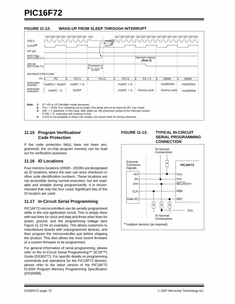
PIC16F72
FIGURE 11-12: WAKE-UP FROM SLEEP THROUGH INTERRUPT
11.15 Program Verification/Code Protection
If the code protection bit(s) have not been pro-grammed, the on-chip program memory can be readout for verification purposes.
11.16 ID Locations
Four memory locations (2000h - 2003h) are designatedas ID locations, where the user can store checksum orother code identification numbers. These locations arenot accessible during normal execution, but are read-able and writable during program/verify. It is recom-mended that only the four Least Significant bits of theID location are used.
11.17 In-Circuit Serial Programming
PIC16F72 microcontrollers can be serially programmedwhile in the end application circuit. This is simply donewith two lines for clock and data and three other lines forpower, ground, and the programming voltage (seeFigure 11-13 for an example). This allows customers tomanufacture boards with unprogrammed devices, andthen program the microcontroller just before shippingthe product. This also allows the most recent firmwareor a custom firmware to be programmed.
For general information of serial programming, pleaserefer to the In-Circuit Serial Programming™ (ICSP™)Guide (DS30277). For specific details on programmingcommands and operations for the PIC16F72 devices,please refer to the latest version of the PIC16F72FLASH Program Memory Programming Specification(DS39588).
FIGURE 11-13: TYPICAL IN-CIRCUIT SERIAL PROGRAMMING CONNECTION
Q1 Q2 Q3 Q4 Q1 Q2 Q3 Q4 Q1 Q1 Q2 Q3 Q4 Q1 Q2 Q3 Q4 Q1 Q2 Q3 Q4 Q1 Q2 Q3 Q4
OSC1
CLKO(4)
INT pin
INTF Flag(INTCON<1>)
GIE bit(INTCON<7>)
INSTRUCTION FLOW
PC
InstructionFetchedInstructionExecuted
PC PC+1 PC+2
Inst(PC) = SLEEP
Inst(PC - 1)
Inst(PC + 1)
SLEEP
Processor in
SLEEP
Interrupt Latency(Note 2)
Inst(PC + 2)
Inst(PC + 1)
Inst(0004h) Inst(0005h)
Inst(0004h)Dummy cycle
PC + 2 0004h 0005h
Dummy cycle
TOST(2)
PC+2
Note 1: XT, HS or LP Oscillator mode assumed.2: TOST = 1024 TOSC (drawing not to scale) This delay will not be there for RC Osc mode.3: GIE = ‘1' assumed. In this case, after wake-up, the processor jumps to the interrupt routine.
If GIE = ‘0', execution will continue in-line.4: CLKO is not available in these Osc modes, but shown here for timing reference.
ExternalConnectorSignals
To NormalConnections
To NormalConnections
PIC16F72
VDD
VSS
MCLR/VPP
RB6
RB7
+5V
0V
VPP
CLK
Data I/O
VDD
* * *
*
* Isolation devices (as required).
DS39597C-page 72 © 2007 Microchip Technology Inc.
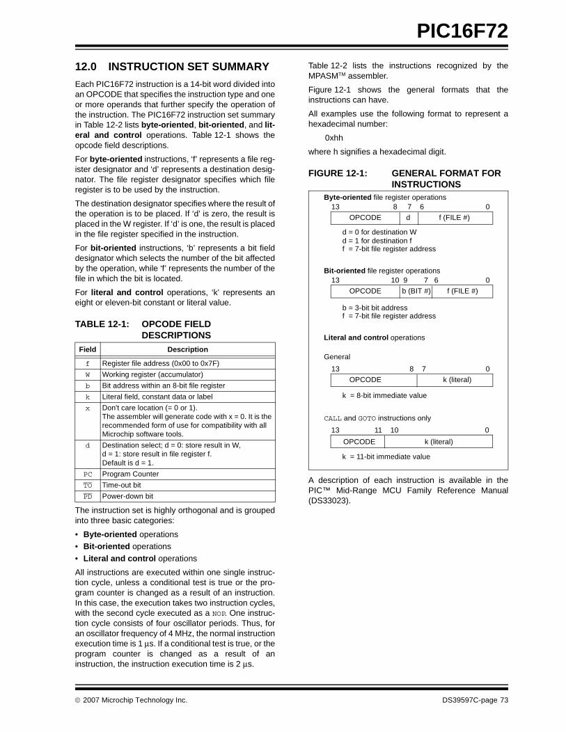
PIC16F72
12.0 INSTRUCTION SET SUMMARY
Each PIC16F72 instruction is a 14-bit word divided intoan OPCODE that specifies the instruction type and oneor more operands that further specify the operation ofthe instruction. The PIC16F72 instruction set summaryin Table 12-2 lists byte-oriented, bit-oriented, and lit-eral and control operations. Table 12-1 shows theopcode field descriptions.
For byte-oriented instructions, ‘f’ represents a file reg-ister designator and ‘d’ represents a destination desig-nator. The file register designator specifies which fileregister is to be used by the instruction.
The destination designator specifies where the result ofthe operation is to be placed. If ‘d’ is zero, the result isplaced in the W register. If ‘d’ is one, the result is placedin the file register specified in the instruction.
For bit-oriented instructions, ‘b’ represents a bit fielddesignator which selects the number of the bit affectedby the operation, while ‘f’ represents the number of thefile in which the bit is located.
For literal and control operations, ‘k’ represents aneight or eleven-bit constant or literal value.
TABLE 12-1: OPCODE FIELD DESCRIPTIONS
The instruction set is highly orthogonal and is groupedinto three basic categories:
• Byte-oriented operations• Bit-oriented operations
• Literal and control operations
All instructions are executed within one single instruc-tion cycle, unless a conditional test is true or the pro-gram counter is changed as a result of an instruction.In this case, the execution takes two instruction cycles,with the second cycle executed as a NOP. One instruc-tion cycle consists of four oscillator periods. Thus, foran oscillator frequency of 4 MHz, the normal instructionexecution time is 1 μs. If a conditional test is true, or theprogram counter is changed as a result of aninstruction, the instruction execution time is 2 μs.
Table 12-2 lists the instructions recognized by theMPASMTM assembler.
Figure 12-1 shows the general formats that theinstructions can have.
All examples use the following format to represent ahexadecimal number:
0xhh
where h signifies a hexadecimal digit.
FIGURE 12-1: GENERAL FORMAT FOR INSTRUCTIONS
A description of each instruction is available in thePIC™ Mid-Range MCU Family Reference Manual(DS33023).
Field Description
f Register file address (0x00 to 0x7F)
W Working register (accumulator)
b Bit address within an 8-bit file register
k Literal field, constant data or label
x Don't care location (= 0 or 1). The assembler will generate code with x = 0. It is the recommended form of use for compatibility with all Microchip software tools.
d Destination select; d = 0: store result in W,d = 1: store result in file register f. Default is d = 1.
PC Program Counter
TO Time-out bit
PD Power-down bit
Byte-oriented file register operations13 8 7 6 0
d = 0 for destination W
OPCODE d f (FILE #)
d = 1 for destination ff = 7-bit file register address
Bit-oriented file register operations13 10 9 7 6 0
OPCODE b (BIT #) f (FILE #)
b = 3-bit bit addressf = 7-bit file register address
Literal and control operations
13 8 7 0
OPCODE k (literal)
k = 8-bit immediate value
13 11 10 0
OPCODE k (literal)
k = 11-bit immediate value
General
CALL and GOTO instructions only
© 2007 Microchip Technology Inc. DS39597C-page 73
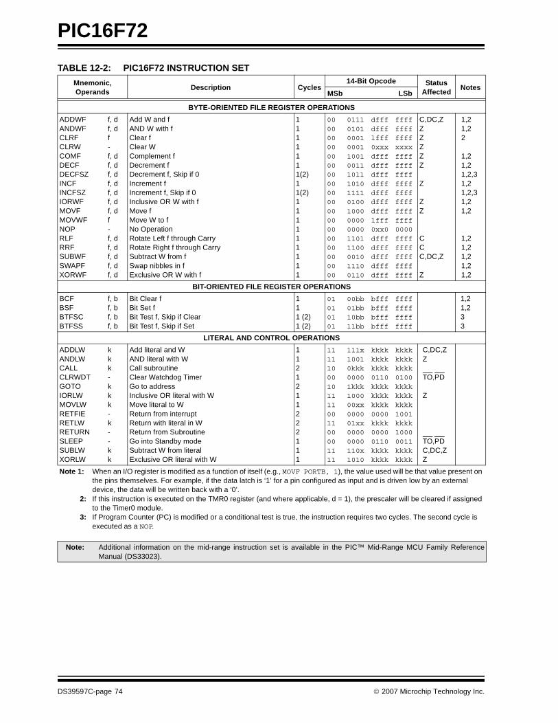
PIC16F72
TABLE 12-2: PIC16F72 INSTRUCTION SET
Mnemonic,Operands
Description Cycles14-Bit Opcode Status
AffectedNotes
MSb LSb
BYTE-ORIENTED FILE REGISTER OPERATIONS
ADDWFANDWFCLRFCLRWCOMFDECFDECFSZINCFINCFSZIORWFMOVFMOVWFNOPRLFRRFSUBWFSWAPFXORWF
f, df, df-f, df, df, df, df, df, df, df-f, df, df, df, df, d
Add W and fAND W with fClear fClear WComplement fDecrement fDecrement f, Skip if 0Increment fIncrement f, Skip if 0Inclusive OR W with fMove fMove W to fNo OperationRotate Left f through CarryRotate Right f through CarrySubtract W from fSwap nibbles in fExclusive OR W with f
1111111(2)11(2)111111111
000000000000000000000000000000000000
011101010001000110010011101110101111010010000000000011011100001011100110
dfffdffflfff0xxxdfffdfffdfffdfffdfffdfffdffflfff0xx0dfffdfffdfffdfffdfff
ffffffffffffxxxxffffffffffffffffffffffffffffffff0000ffffffffffffffffffff
C,DC,ZZZZZZ
Z
ZZ
CCC,DC,Z
Z
1,21,22
1,21,21,2,31,21,2,31,21,2
1,21,21,21,21,2
BIT-ORIENTED FILE REGISTER OPERATIONS
BCFBSFBTFSCBTFSS
f, bf, bf, bf, b
Bit Clear fBit Set fBit Test f, Skip if ClearBit Test f, Skip if Set
111 (2)1 (2)
01010101
00bb01bb10bb11bb
bfffbfffbfffbfff
ffffffffffffffff
1,21,233
LITERAL AND CONTROL OPERATIONS
ADDLWANDLWCALLCLRWDTGOTOIORLWMOVLWRETFIERETLWRETURNSLEEPSUBLWXORLW
kkk-kkk-k--kk
Add literal and WAND literal with WCall subroutineClear Watchdog TimerGo to addressInclusive OR literal with WMove literal to WReturn from interruptReturn with literal in W Return from SubroutineGo into Standby modeSubtract W from literalExclusive OR literal with W
1121211222111
11111000101111001100001111
111x10010kkk00001kkk100000xx000001xx00000000110x1010
kkkkkkkkkkkk0110kkkkkkkkkkkk0000kkkk00000110kkkkkkkk
kkkkkkkkkkkk0100kkkkkkkkkkkk1001kkkk10000011kkkkkkkk
C,DC,ZZ
TO,PD
Z
TO,PDC,DC,ZZ
Note 1: When an I/O register is modified as a function of itself (e.g., MOVF PORTB, 1), the value used will be that value present on the pins themselves. For example, if the data latch is ‘1’ for a pin configured as input and is driven low by an external device, the data will be written back with a ‘0’.
2: If this instruction is executed on the TMR0 register (and where applicable, d = 1), the prescaler will be cleared if assigned to the Timer0 module.
3: If Program Counter (PC) is modified or a conditional test is true, the instruction requires two cycles. The second cycle is executed as a NOP.
Note: Additional information on the mid-range instruction set is available in the PIC™ Mid-Range MCU Family ReferenceManual (DS33023).
DS39597C-page 74 © 2007 Microchip Technology Inc.
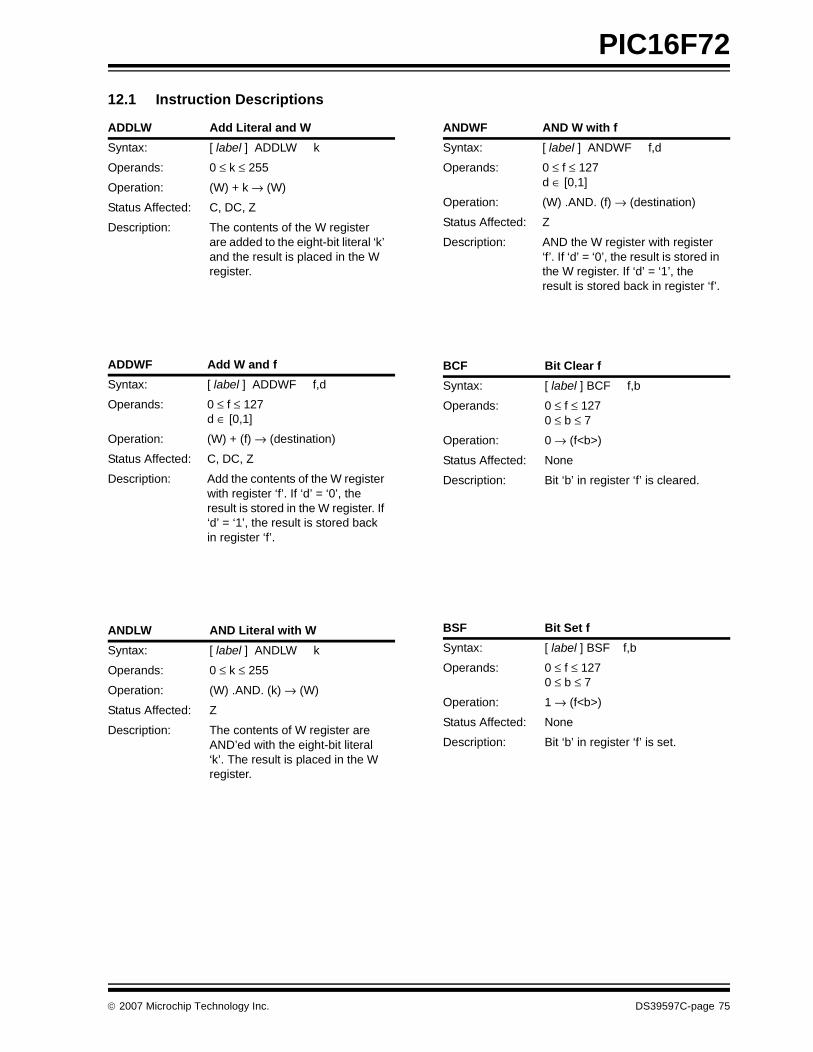
PIC16F72
12.1 Instruction Descriptions
ADDLW Add Literal and W
Syntax: [ label ] ADDLW k
Operands: 0 ≤ k ≤ 255
Operation: (W) + k → (W)
Status Affected: C, DC, Z
Description: The contents of the W register are added to the eight-bit literal ‘k’ and the result is placed in the W register.
ADDWF Add W and f
Syntax: [ label ] ADDWF f,d
Operands: 0 ≤ f ≤ 127d ∈ [0,1]
Operation: (W) + (f) → (destination)
Status Affected: C, DC, Z
Description: Add the contents of the W register with register ‘f’. If ‘d’ = ‘0’, the result is stored in the W register. If ‘d’ = ‘1’, the result is stored back in register ‘f’.
ANDLW AND Literal with W
Syntax: [ label ] ANDLW k
Operands: 0 ≤ k ≤ 255
Operation: (W) .AND. (k) → (W)
Status Affected: Z
Description: The contents of W register are AND’ed with the eight-bit literal ‘k’. The result is placed in the W register.
ANDWF AND W with f
Syntax: [ label ] ANDWF f,d
Operands: 0 ≤ f ≤ 127d ∈ [0,1]
Operation: (W) .AND. (f) → (destination)
Status Affected: Z
Description: AND the W register with register ‘f’. If ‘d’ = ‘0’, the result is stored in the W register. If ‘d’ = ‘1’, the result is stored back in register ‘f’.
BCF Bit Clear f
Syntax: [ label ] BCF f,b
Operands: 0 ≤ f ≤ 1270 ≤ b ≤ 7
Operation: 0 → (f<b>)
Status Affected: None
Description: Bit ‘b’ in register ‘f’ is cleared.
BSF Bit Set f
Syntax: [ label ] BSF f,b
Operands: 0 ≤ f ≤ 1270 ≤ b ≤ 7
Operation: 1 → (f<b>)
Status Affected: None
Description: Bit ‘b’ in register ‘f’ is set.
© 2007 Microchip Technology Inc. DS39597C-page 75
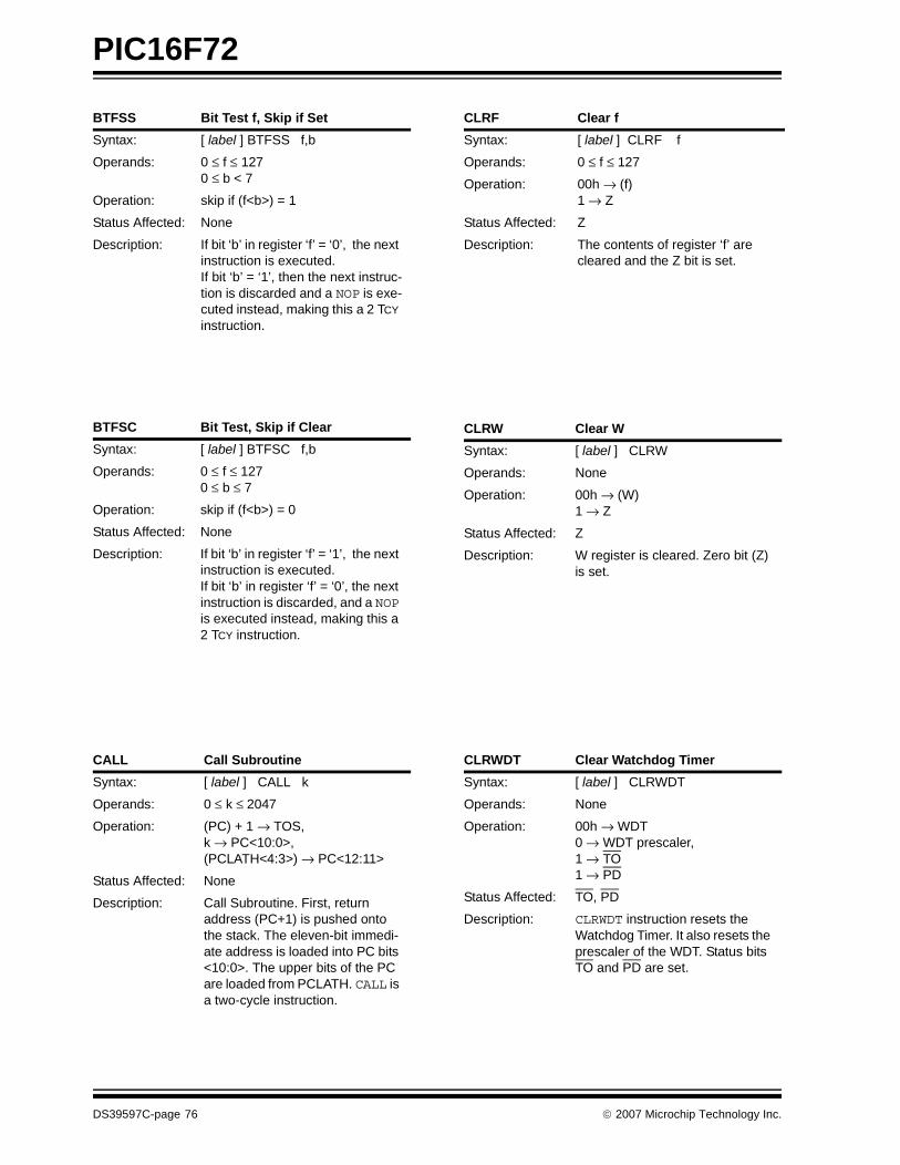
PIC16F72
BTFSS Bit Test f, Skip if Set
Syntax: [ label ] BTFSS f,b
Operands: 0 ≤ f ≤ 1270 ≤ b < 7
Operation: skip if (f<b>) = 1
Status Affected: None
Description: If bit ‘b’ in register ‘f’ = ‘0’, the next instruction is executed.If bit ‘b’ = ‘1’, then the next instruc-tion is discarded and a NOP is exe-cuted instead, making this a 2 TCY instruction.
BTFSC Bit Test, Skip if Clear
Syntax: [ label ] BTFSC f,b
Operands: 0 ≤ f ≤ 1270 ≤ b ≤ 7
Operation: skip if (f<b>) = 0
Status Affected: None
Description: If bit ‘b’ in register ‘f’ = ‘1’, the next instruction is executed.If bit ‘b’ in register ‘f’ = ‘0’, the next instruction is discarded, and a NOP is executed instead, making this a 2 TCY instruction.
CALL Call Subroutine
Syntax: [ label ] CALL k
Operands: 0 ≤ k ≤ 2047
Operation: (PC) + 1 → TOS,k → PC<10:0>,(PCLATH<4:3>) → PC<12:11>
Status Affected: None
Description: Call Subroutine. First, return address (PC+1) is pushed onto the stack. The eleven-bit immedi-ate address is loaded into PC bits <10:0>. The upper bits of the PC are loaded from PCLATH. CALL is a two-cycle instruction.
CLRF Clear f
Syntax: [ label ] CLRF f
Operands: 0 ≤ f ≤ 127
Operation: 00h → (f)1 → Z
Status Affected: Z
Description: The contents of register ‘f’ are cleared and the Z bit is set.
CLRW Clear W
Syntax: [ label ] CLRW
Operands: None
Operation: 00h → (W)1 → Z
Status Affected: Z
Description: W register is cleared. Zero bit (Z) is set.
CLRWDT Clear Watchdog Timer
Syntax: [ label ] CLRWDT
Operands: None
Operation: 00h → WDT0 → WDT prescaler,1 → TO1 → PD
Status Affected: TO, PD
Description: CLRWDT instruction resets the Watchdog Timer. It also resets the prescaler of the WDT. Status bits TO and PD are set.
DS39597C-page 76 © 2007 Microchip Technology Inc.
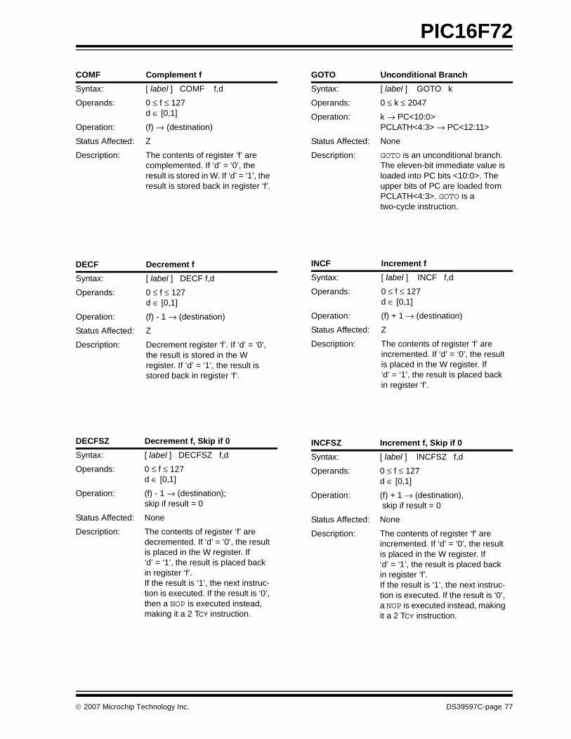
PIC16F72
COMF Complement f
Syntax: [ label ] COMF f,d
Operands: 0 ≤ f ≤ 127d ∈ [0,1]
Operation: (f) → (destination)
Status Affected: Z
Description: The contents of register ‘f’ are complemented. If ‘d’ = ‘0’, the result is stored in W. If ‘d’ = ‘1’, the result is stored back in register ‘f’.
DECF Decrement f
Syntax: [ label ] DECF f,d
Operands: 0 ≤ f ≤ 127d ∈ [0,1]
Operation: (f) - 1 → (destination)
Status Affected: Z
Description: Decrement register ‘f’. If ‘d’ = ‘0’, the result is stored in the W register. If ‘d’ = ‘1’, the result is stored back in register ‘f’.
DECFSZ Decrement f, Skip if 0
Syntax: [ label ] DECFSZ f,d
Operands: 0 ≤ f ≤ 127d ∈ [0,1]
Operation: (f) - 1 → (destination); skip if result = 0
Status Affected: None
Description: The contents of register ‘f’ are decremented. If ‘d’ = ‘0’, the result is placed in the W register. If ‘d’ = ‘1’, the result is placed back in register ‘f’. If the result is ‘1’, the next instruc-tion is executed. If the result is ‘0’, then a NOP is executed instead, making it a 2 TCY instruction.
GOTO Unconditional Branch
Syntax: [ label ] GOTO k
Operands: 0 ≤ k ≤ 2047
Operation: k → PC<10:0>PCLATH<4:3> → PC<12:11>
Status Affected: None
Description: GOTO is an unconditional branch. The eleven-bit immediate value is loaded into PC bits <10:0>. The upper bits of PC are loaded from PCLATH<4:3>. GOTO is a two-cycle instruction.
INCF Increment f
Syntax: [ label ] INCF f,d
Operands: 0 ≤ f ≤ 127d ∈ [0,1]
Operation: (f) + 1 → (destination)
Status Affected: Z
Description: The contents of register ‘f’ are incremented. If ‘d’ = ‘0’, the result is placed in the W register. If ‘d’ = ‘1’, the result is placed back in register ‘f’.
INCFSZ Increment f, Skip if 0
Syntax: [ label ] INCFSZ f,d
Operands: 0 ≤ f ≤ 127d ∈ [0,1]
Operation: (f) + 1 → (destination), skip if result = 0
Status Affected: None
Description: The contents of register ‘f’ are incremented. If ‘d’ = ‘0’, the result is placed in the W register. If ‘d’ = ‘1’, the result is placed back in register ‘f’.If the result is ‘1’, the next instruc-tion is executed. If the result is ‘0’, a NOP is executed instead, making it a 2 TCY instruction.
© 2007 Microchip Technology Inc. DS39597C-page 77
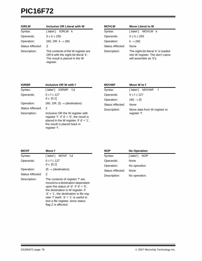
PIC16F72
IORLW Inclusive OR Literal with W
Syntax: [ label ] IORLW k
Operands: 0 ≤ k ≤ 255
Operation: (W) .OR. k → (W)
Status Affected: Z
Description: The contents of the W register are OR’d with the eight-bit literal ‘k’. The result is placed in the W register.
IORWF Inclusive OR W with f
Syntax: [ label ] IORWF f,d
Operands: 0 ≤ f ≤ 127d ∈ [0,1]
Operation: (W) .OR. (f) → (destination)
Status Affected: Z
Description: Inclusive OR the W register with register ‘f’. If ‘d’ = ‘0’, the result is placed in the W register. If ‘d’ = ‘1’, the result is placed back in register ‘f’.
MOVF Move f
Syntax: [ label ] MOVF f,d
Operands: 0 ≤ f ≤ 127d ∈ [0,1]
Operation: (f) → (destination)
Status Affected: Z
Description: The contents of register ‘f’ are moved to a destination dependant upon the status of ‘d’. If ‘d’ = ‘0’, the destination is W register. If ‘d’ = ‘1’, the destination is file reg-ister ‘f’ itself. ‘d’ = ‘1’ is useful to test a file register, since status flag Z is affected.
MOVLW Move Literal to W
Syntax: [ label ] MOVLW k
Operands: 0 ≤ k ≤ 255
Operation: k → (W)
Status Affected: None
Description: The eight-bit literal ‘k’ is loaded into W register. The don’t cares will assemble as ‘0’s.
MOVWF Move W to f
Syntax: [ label ] MOVWF f
Operands: 0 ≤ f ≤ 127
Operation: (W) → (f)
Status Affected: None
Description: Move data from W register to register ‘f’.
NOP No Operation
Syntax: [ label ] NOP
Operands: None
Operation: No operation
Status Affected: None
Description: No operation.
DS39597C-page 78 © 2007 Microchip Technology Inc.
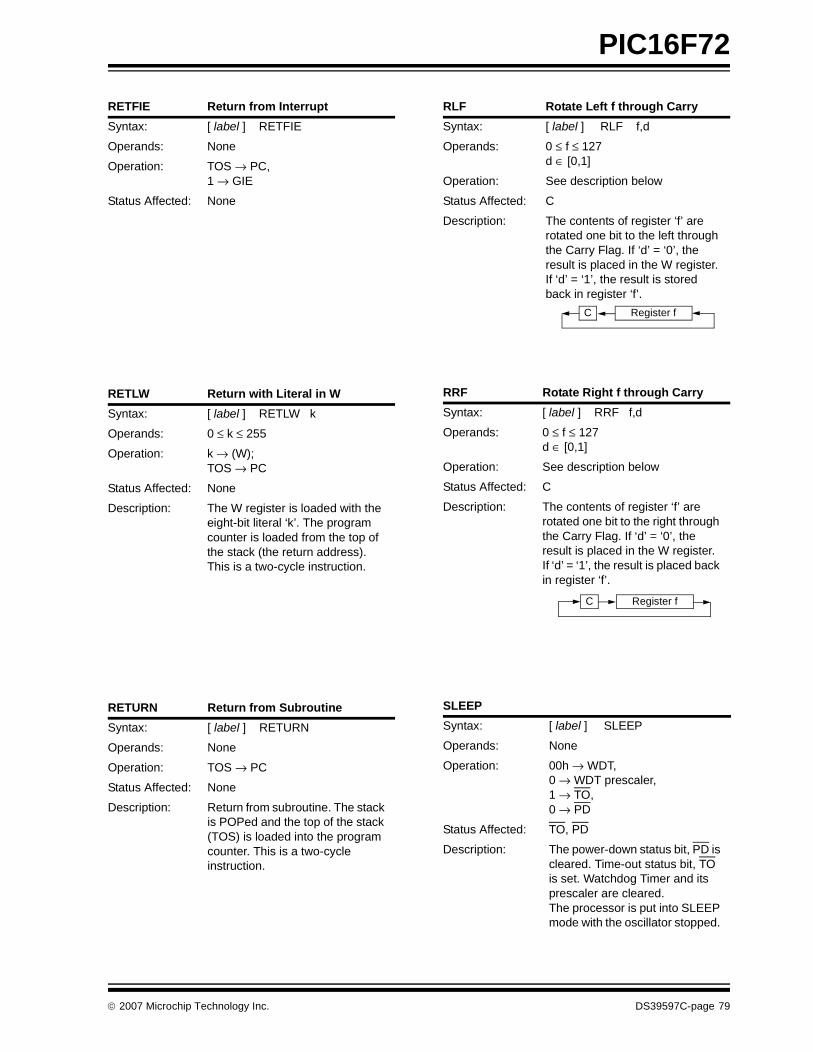
PIC16F72
RETFIE Return from Interrupt
Syntax: [ label ] RETFIE
Operands: None
Operation: TOS → PC,1 → GIE
Status Affected: None
RETLW Return with Literal in W
Syntax: [ label ] RETLW k
Operands: 0 ≤ k ≤ 255
Operation: k → (W); TOS → PC
Status Affected: None
Description: The W register is loaded with the eight-bit literal ‘k’. The program counter is loaded from the top of the stack (the return address). This is a two-cycle instruction.
RETURN Return from Subroutine
Syntax: [ label ] RETURN
Operands: None
Operation: TOS → PC
Status Affected: None
Description: Return from subroutine. The stack is POPed and the top of the stack (TOS) is loaded into the program counter. This is a two-cycle instruction.
RLF Rotate Left f through Carry
Syntax: [ label ] RLF f,d
Operands: 0 ≤ f ≤ 127d ∈ [0,1]
Operation: See description below
Status Affected: C
Description: The contents of register ‘f’ are rotated one bit to the left through the Carry Flag. If ‘d’ = ‘0’, the result is placed in the W register. If ‘d’ = ‘1’, the result is stored back in register ‘f’.
RRF Rotate Right f through Carry
Syntax: [ label ] RRF f,d
Operands: 0 ≤ f ≤ 127d ∈ [0,1]
Operation: See description below
Status Affected: C
Description: The contents of register ‘f’ are rotated one bit to the right through the Carry Flag. If ‘d’ = ‘0’, the result is placed in the W register. If ‘d’ = ‘1’, the result is placed back in register ‘f’.
SLEEP
Syntax: [ label ] SLEEP
Operands: None
Operation: 00h → WDT,0 → WDT prescaler,1 → TO,0 → PD
Status Affected: TO, PD
Description: The power-down status bit, PD is cleared. Time-out status bit, TO is set. Watchdog Timer and its prescaler are cleared.The processor is put into SLEEP mode with the oscillator stopped.
Register fC
Register fC
© 2007 Microchip Technology Inc. DS39597C-page 79
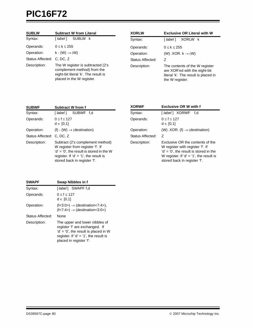
PIC16F72
SUBLW Subtract W from LiteralSyntax: [ label ] SUBLW k
Operands: 0 ≤ k ≤ 255
Operation: k - (W) → (W)
Status Affected: C, DC, Z
Description: The W register is subtracted (2’s complement method) from the eight-bit literal ‘k’. The result is placed in the W register.
SUBWF Subtract W from fSyntax: [ label ] SUBWF f,d
Operands: 0 ≤ f ≤ 127d ∈ [0,1]
Operation: (f) - (W) → (destination)
Status Affected: C, DC, Z
Description: Subtract (2’s complement method) W register from register ‘f’. If ‘d’ = ‘0’, the result is stored in the W register. If ‘d’ = ‘1’, the result is stored back in register ‘f’.
SWAPF Swap Nibbles in f
Syntax: [ label ] SWAPF f,d
Operands: 0 ≤ f ≤ 127d ∈ [0,1]
Operation: (f<3:0>) → (destination<7:4>),(f<7:4>) → (destination<3:0>)
Status Affected: None
Description: The upper and lower nibbles of register ‘f’ are exchanged. If ‘d’ = ‘0’, the result is placed in W register. If ‘d’ = ‘1’, the result is placed in register ‘f’.
XORLW Exclusive OR Literal with W
Syntax: [ label ] XORLW k
Operands: 0 ≤ k ≤ 255
Operation: (W) .XOR. k → (W)
Status Affected: Z
Description: The contents of the W register are XOR’ed with the eight-bit literal ‘k’. The result is placed in the W register.
XORWF Exclusive OR W with f
Syntax: [ label ] XORWF f,d
Operands: 0 ≤ f ≤ 127d ∈ [0,1]
Operation: (W) .XOR. (f) → (destination)
Status Affected: Z
Description: Exclusive OR the contents of the W register with register ‘f’. If ‘d’ = ‘0’, the result is stored in the W register. If ‘d’ = ‘1’, the result is stored back in register ‘f’.
DS39597C-page 80 © 2007 Microchip Technology Inc.
PIC16F72
13.0 DEVELOPMENT SUPPORT
The PIC® microcontrollers are supported with a fullrange of hardware and software development tools:
• Integrated Development Environment
- MPLAB® IDE Software• Assemblers/Compilers/Linkers
- MPASMTM Assembler
- MPLAB C17 and MPLAB C18 C Compilers- MPLINKTM Object Linker/
MPLIBTM Object Librarian• Simulators
- MPLAB SIM Software Simulator
• Emulators- MPLAB ICE 2000 In-Circuit Emulator- ICEPIC™ In-Circuit Emulator
• In-Circuit Debugger- MPLAB ICD
• Device Programmers
- PRO MATE® II Universal Device Programmer- PICSTART® Plus Entry-Level Development
Programmer• Low Cost Demonstration Boards
- PICDEMTM 1 Demonstration Board
- PICDEM 2 Demonstration Board- PICDEM 3 Demonstration Board- PICDEM 17 Demonstration Board
- KEELOQ® Demonstration Board
13.1 MPLAB Integrated Development Environment Software
The MPLAB IDE software brings an ease of softwaredevelopment previously unseen in the 8-bit microcon-troller market. The MPLAB IDE is a Windows®-basedapplication that contains:
• An interface to debugging tools- simulator
- programmer (sold separately)- emulator (sold separately)- in-circuit debugger (sold separately)
• A full-featured editor• A project manager• Customizable toolbar and key mapping
• A status bar• On-line help
The MPLAB IDE allows you to:
• Edit your source files (either assembly or ‘C’)• One touch assemble (or compile) and download
to PIC emulator and simulator tools (automatically updates all project information)
• Debug using:- source files
- absolute listing file- machine code
The ability to use MPLAB IDE with multiple debuggingtools allows users to easily switch from the cost-effective simulator to a full-featured emulator withminimal retraining.
13.2 MPASM Assembler
The MPASM assembler is a full-featured universalmacro assembler for all PIC MCU’s.
The MPASM assembler has a command line interfaceand a Windows shell. It can be used as a stand-aloneapplication on a Windows 3.x or greater system, or itcan be used through MPLAB IDE. The MPASM assem-bler generates relocatable object files for the MPLINKobject linker, Intel® standard HEX files, MAP files todetail memory usage and symbol reference, an abso-lute LST file that contains source lines and generatedmachine code, and a COD file for debugging.
The MPASM assembler features include:
• Integration into MPLAB IDE projects.• User-defined macros to streamline assembly
code.• Conditional assembly for multi-purpose source
files.• Directives that allow complete control over the
assembly process.
13.3 MPLAB C17 and MPLAB C18 C Compilers
The MPLAB C17 and MPLAB C18 Code DevelopmentSystems are complete ANSI ‘C’ compilers forMicrochip’s PIC17CXXX and PIC18CXXX family ofmicrocontrollers, respectively. These compilers providepowerful integration capabilities and ease of use notfound with other compilers.
For easier source level debugging, the compilers pro-vide symbol information that is compatible with theMPLAB IDE memory display.
© 2007 Microchip Technology Inc. DS39597C-page 81
PIC16F72
13.4 MPLINK Object Linker/MPLIB Object Librarian
The MPLINK object linker combines relocatableobjects created by the MPASM assembler and theMPLAB C17 and MPLAB C18 C compilers. It can alsolink relocatable objects from pre-compiled libraries,using directives from a linker script.
The MPLIB object librarian is a librarian for pre-compiled code to be used with the MPLINK objectlinker. When a routine from a library is called fromanother source file, only the modules that contain thatroutine will be linked in with the application. This allowslarge libraries to be used efficiently in many differentapplications. The MPLIB object librarian manages thecreation and modification of library files.
The MPLINK object linker features include:
• Integration with MPASM assembler and MPLAB C17 and MPLAB C18 C compilers.
• Allows all memory areas to be defined as sections to provide link-time flexibility.
The MPLIB object librarian features include:
• Easier linking because single libraries can be included instead of many smaller files.
• Helps keep code maintainable by grouping related modules together.
• Allows libraries to be created and modules to be added, listed, replaced, deleted or extracted.
13.5 MPLAB SIM Software Simulator
The MPLAB SIM software simulator allows code devel-opment in a PC-hosted environment by simulating thePIC series microcontrollers on an instruction level. Onany given instruction, the data areas can be examinedor modified and stimuli can be applied from a file, oruser-defined key press, to any of the pins. The execu-tion can be performed in single step, execute untilbreak, or trace mode.
The MPLAB SIM simulator fully supports symbolic debug-ging using the MPLAB C17 and the MPLAB C18 C com-pilers and the MPASM assembler. The software simulatoroffers the flexibility to develop and debug code outside ofthe laboratory environment, making it an excellent multi-project software development tool.
13.6 MPLAB ICE High Performance Universal In-Circuit Emulator with MPLAB IDE
The MPLAB ICE universal in-circuit emulator is intendedto provide the product development engineer with acomplete microcontroller design tool set for PIC micro-controllers (MCUs). Software control of the MPLAB ICEin-circuit emulator is provided by the MPLAB IntegratedDevelopment Environment (IDE), which allows editing,building, downloading and source debugging from asingle environment.
The MPLAB ICE 2000 is a full-featured emulator sys-tem with enhanced trace, trigger and data monitoringfeatures. Interchangeable processor modules allow thesystem to be easily reconfigured for emulation of differ-ent processors. The universal architecture of theMPLAB ICE in-circuit emulator allows expansion tosupport new PIC microcontrollers.
The MPLAB ICE in-circuit emulator system has beendesigned as a real-time emulation system, withadvanced features that are generally found on moreexpensive development tools. The PC platform andMicrosoft® Windows environment were chosen to bestmake these features available to you, the end user.
13.7 ICEPIC In-Circuit Emulator
The ICEPIC low cost, in-circuit emulator is a solutionfor the Microchip Technology PIC16C5X, PIC16C6X,PIC16C7X and PIC16CXXX families of 8-bit One-Time-Programmable (OTP) microcontrollers. The mod-ular system can support different subsets of PIC16C5Xor PIC16CXXX products through the use of inter-changeable personality modules, or daughter boards.The emulator is capable of emulating without targetapplication circuitry being present.
DS39597C-page 82 © 2007 Microchip Technology Inc.
PIC16F72
13.8 MPLAB ICD In-Circuit Debugger
Microchip's In-Circuit Debugger, MPLAB ICD, is a pow-erful, low cost, run-time development tool. This tool isbased on the FLASH PIC MCUs and can be used todevelop for this and other PIC microcontrollers. TheMPLAB ICD utilizes the in-circuit debugging capabilitybuilt into the FLASH devices. This feature, along withMicrochip's In-Circuit Serial ProgrammingTM protocol,offers cost-effective in-circuit FLASH debugging fromthe graphical user interface of the MPLAB IntegratedDevelopment Environment. This enables a designer todevelop and debug source code by watching variables,single-stepping and setting break points. Running atfull speed enables testing hardware in real-time.
13.9 PRO MATE II Universal Device Programmer
The PRO MATE II universal device programmer is afull-featured programmer, capable of operating instand-alone mode, as well as PC-hosted mode. ThePRO MATE II device programmer is CE compliant.
The PRO MATE II device programmer has program-mable VDD and VPP supplies, which allow it to verifyprogrammed memory at VDD min and VDD max for max-imum reliability. It has an LCD display for instructionsand error messages, keys to enter commands and amodular detachable socket assembly to support variouspackage types. In stand-alone mode, the PRO MATE IIdevice programmer can read, verify, or program PICdevices. It can also set code protection in this mode.
13.10 PICSTART Plus Entry Level Development Programmer
The PICSTART Plus development programmer is aneasy-to-use, low cost, prototype programmer. It con-nects to the PC via a COM (RS-232) port. MPLABIntegrated Development Environment software makesusing the programmer simple and efficient.
The PICSTART Plus development programmer sup-ports all PIC devices with up to 40 pins. Larger pincount devices, such as the PIC16C92X andPIC17C76X, may be supported with an adapter socket.The PICSTART Plus development programmer is CEcompliant.
13.11 PICDEM 1 Low Cost PICDemonstration Board
The PICDEM 1 demonstration board is a simple boardwhich demonstrates the capabilities of several ofMicrochip’s microcontrollers. The microcontrollers sup-ported are: PIC16C5X (PIC16C54 to PIC16C58A),PIC16C61, PIC16C62X, PIC16C71, PIC16C8X,PIC17C42, PIC17C43 and PIC17C44. All necessaryhardware and software is included to run basic demoprograms. The user can program the sample microcon-trollers provided with the PICDEM 1 demonstrationboard on a PRO MATE II device programmer, or aPICSTART Plus development programmer, and easilytest firmware. The user can also connect thePICDEM 1 demonstration board to the MPLAB ICE in-circuit emulator and download the firmware to the emu-lator for testing. A prototype area is available for theuser to build some additional hardware and connect itto the microcontroller socket(s). Some of the featuresinclude an RS-232 interface, a potentiometer for simu-lated analog input, push button switches and eightLEDs connected to PORTB.
13.12 PICDEM 2 Low Cost PIC16CXX Demonstration Board
The PICDEM 2 demonstration board is a simple dem-onstration board that supports the PIC16C62,PIC16C64, PIC16C65, PIC16C73 and PIC16C74microcontrollers. All the necessary hardware and soft-ware is included to run the basic demonstration pro-grams. The user can program the samplemicrocontrollers provided with the PICDEM 2 demon-stration board on a PRO MATE II device programmer,or a PICSTART Plus development programmer, andeasily test firmware. The MPLAB ICE in-circuit emula-tor may also be used with the PICDEM 2 demonstrationboard to test firmware. A prototype area has been pro-vided to the user for adding additional hardware andconnecting it to the microcontroller socket(s). Some ofthe features include a RS-232 interface, push buttonswitches, a potentiometer for simulated analog input, aserial EEPROM to demonstrate usage of the I2CTM busand separate headers for connection to an LCDmodule and a keypad.
© 2007 Microchip Technology Inc. DS39597C-page 83
PIC16F72
13.13 PICDEM 3 Low Cost PIC16CXXX Demonstration Board
The PICDEM 3 demonstration board is a simple dem-onstration board that supports the PIC16C923 andPIC16C924 in the PLCC package. It will also supportfuture 44-pin PLCC microcontrollers with an LCD Mod-ule. All the necessary hardware and software isincluded to run the basic demonstration programs. Theuser can program the sample microcontrollers pro-vided with the PICDEM 3 demonstration board on aPRO MATE II device programmer, or a PICSTART Plusdevelopment programmer with an adapter socket, andeasily test firmware. The MPLAB ICE in-circuit emula-tor may also be used with the PICDEM 3 demonstrationboard to test firmware. A prototype area has been pro-vided to the user for adding hardware and connecting itto the microcontroller socket(s). Some of the featuresinclude a RS-232 interface, push button switches, apotentiometer for simulated analog input, a thermistorand separate headers for connection to an externalLCD module and a keypad. Also provided on thePICDEM 3 demonstration board is a LCD panel, with 4commons and 12 segments, that is capable of display-ing time, temperature and day of the week. ThePICDEM 3 demonstration board provides an additionalRS-232 interface and Windows software for showingthe demultiplexed LCD signals on a PC. A simple serialinterface allows the user to construct a hardwaredemultiplexer for the LCD signals.
13.14 PICDEM 17 Demonstration Board
The PICDEM 17 demonstration board is an evaluationboard that demonstrates the capabilities of severalMicrochip microcontrollers, including PIC17C752,PIC17C756A, PIC17C762 and PIC17C766. All neces-sary hardware is included to run basic demo programs,which are supplied on a 3.5-inch disk. A programmedsample is included and the user may erase it andprogram it with the other sample programs using thePRO MATE II device programmer, or the PICSTARTPlus development programmer, and easily debug andtest the sample code. In addition, the PICDEM 17 dem-onstration board supports downloading of programs toand executing out of external FLASH memory on board.The PICDEM 17 demonstration board is also usablewith the MPLAB ICE in-circuit emulator, or thePICMASTER emulator and all of the sample programscan be run and modified using either emulator. Addition-ally, a generous prototype area is available for userhardware.
13.15 KEELOQ Evaluation and Programming Tools
KEELOQ evaluation and programming tools supportMicrochip’s HCS Secure Data Products. The HCS eval-uation kit includes a LCD display to show changingcodes, a decoder to decode transmissions and a pro-gramming interface to program test transmitters.
DS39597C-page 84 © 2007 Microchip Technology Inc.
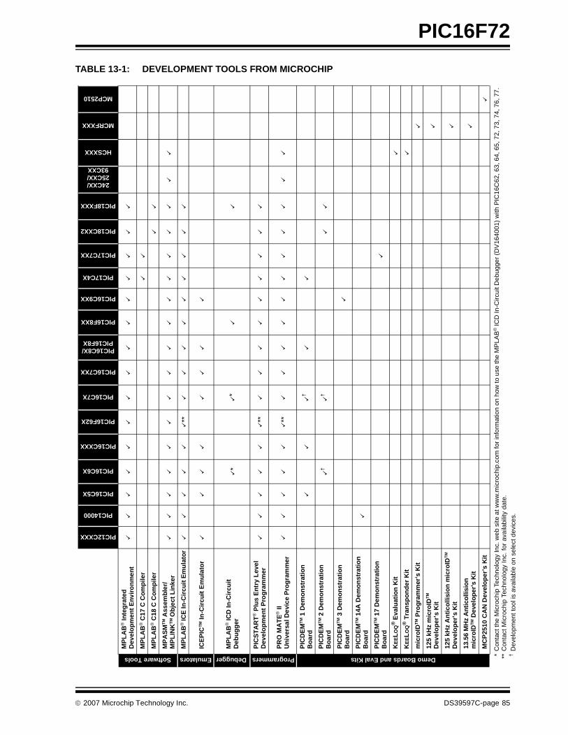
PIC16F72
TABLE 13-1: DEVELOPMENT TOOLS FROM MICROCHIP
PIC12CXXX
PIC14000
PIC16C5X
PIC16C6X
PIC16CXXX
PIC16F62X
PIC16C7X
PIC16C7XX
PIC16C8X/PIC16F8X
PIC16F8XX
PIC16C9XX
PIC17C4X
PIC17C7XX
PIC18CXX2
PIC18FXXX
24CXX/25CXX/93CXX
HCSXXX
MCRFXXX
MCP2510
Software Tools
MP
LA
B® In
teg
rate
dD
evel
op
men
t E
nvi
ron
men
t
MP
LA
B® C
17 C
Co
mp
iler
MP
LA
B® C
18 C
Co
mp
iler
MP
AS
MT
M A
ssem
ble
r/M
PL
INK
TM
Ob
ject
Lin
ker
Emulators
MP
LA
B® IC
E In
-Cir
cuit
Em
ula
tor
**
ICE
PIC
TM In
-Cir
cuit
Em
ula
tor
Debugger
MP
LA
B® IC
D In
-Cir
cuit
D
ebu
gg
er*
*
Programmers
PIC
ST
AR
T® P
lus
En
try
Lev
elD
evel
op
men
t P
rog
ram
mer
**
PR
O M
AT
E® II
U
niv
ersa
l Dev
ice
Pro
gra
mm
er**
Demo Boards and Eval Kits
PIC
DE
MT
M 1
Dem
on
stra
tio
n
Bo
ard
†
PIC
DE
MT
M 2
Dem
on
stra
tio
n
Bo
ard
††
PIC
DE
MT
M 3
Dem
on
stra
tio
n
Bo
ard
PIC
DE
MT
M 1
4A D
emo
nst
rati
on
B
oar
d
PIC
DE
MT
M 1
7 D
emo
nst
rati
on
B
oar
d
KE
EL
OQ
® E
valu
atio
n K
it
KE
EL
OQ
® T
ran
spo
nd
er K
it
mic
roID
TM P
rog
ram
mer
’s K
it
125
kHz
mic
roID
TM
Dev
elo
per
’s K
it
125
kHz
An
tico
llisi
on
mic
roID
TM
Dev
elo
per
’s K
it
13.5
6 M
Hz
An
tico
llisi
on
m
icro
IDT
M D
evel
op
er’s
Kit
MC
P25
10 C
AN
Dev
elo
per
’s K
it
*C
onta
ct th
e M
icro
chip
Tec
hnol
ogy
Inc.
web
site
at w
ww
.mic
roch
ip.c
om fo
r in
form
atio
n on
how
to u
se th
e M
PLA
B® IC
D In
-Circ
uit D
ebug
ger
(DV
1640
01)
with
PIC
16C
62, 6
3, 6
4, 6
5, 7
2, 7
3, 7
4, 7
6, 7
7.**
Con
tact
Mic
roch
ip T
echn
olog
y In
c. fo
r av
aila
bilit
y da
te.
†D
evel
opm
ent t
ool i
s av
aila
ble
on s
elec
t dev
ices
.
© 2007 Microchip Technology Inc. DS39597C-page 85

PIC16F72
NOTES:
DS39597C-page 86 © 2007 Microchip Technology Inc.
PIC16F72
14.0 ELECTRICAL CHARACTERISTICS
Absolute Maximum Ratings †
Ambient temperature under bias................................................................................................................ -55 to +125°C
Storage temperature .............................................................................................................................. -65°C to +150°C
Voltage on any pin with respect to VSS (except VDD, MCLR. and RA4) ......................................... -0.3V to (VDD + 0.3V)
Voltage on VDD with respect to VSS ............................................................................................................ -0.3 to +6.5V
Voltage on MCLR with respect to VSS (Note 2) ..............................................................................................0 to +13.5V
Voltage on RA4 with respect to Vss ...................................................................................................................0 to +12V
Total power dissipation (Note 1) ...............................................................................................................................1.0W
Maximum current out of VSS pin ...........................................................................................................................300 mA
Maximum current into VDD pin ..............................................................................................................................250 mA
Input clamp current, IIK (VI < 0 or VI > VDD)..................................................................................................................... ± 20 mA
Output clamp current, IOK (VO < 0 or VO > VDD) ............................................................................................................. ± 20 mA
Maximum output current sunk by any I/O pin..........................................................................................................25 mA
Maximum output current sourced by any I/O pin ....................................................................................................25 mA
Maximum current sunk by PORTA, PORTB..........................................................................................................200 mA
Maximum current sourced by PORTA, PORTB ....................................................................................................200 mA
Maximum current sunk by PORTC .......................................................................................................................200 mA
Maximum current sourced by PORTC ..................................................................................................................200 mA
Note 1: Power dissipation is calculated as follows: Pdis = VDD x {IDD - ∑ IOH} + ∑ {(VDD - VOH) x IOH} + ∑(VOl x IOL)
2: Voltage spikes at the MCLR pin may cause unpredictable results. A series resistor of greater than 1 kΩshould be used to pull MCLR to VDD, rather than tying the pin directly to VDD.
† NOTICE: Stresses above those listed under “Absolute Maximum Ratings” may cause permanent damage to the device. This is a stress rating only and functional operation of the device at those or any other conditions above those indicated in the operation listings of this specification is not implied. Exposure to maximum rating conditions for extended periods may affect device reliability.
© 2007 Microchip Technology Inc. DS39597C-page 87
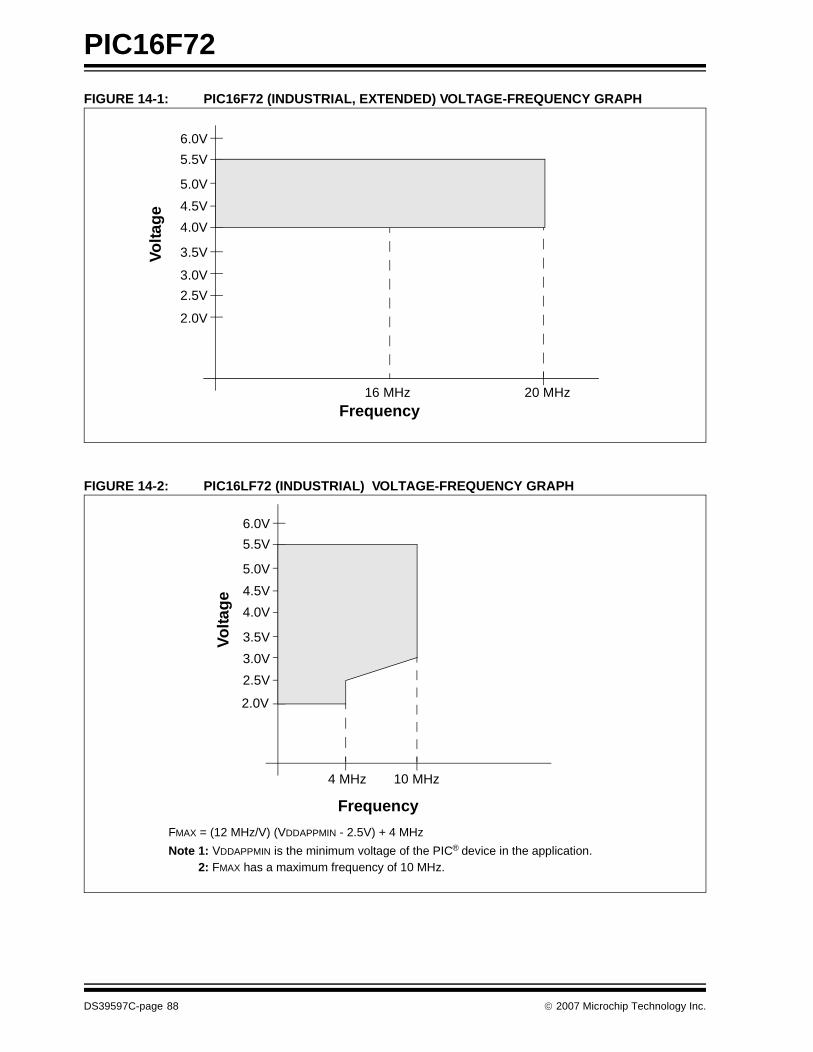
PIC16F72
FIGURE 14-1: PIC16F72 (INDUSTRIAL, EXTENDED) VOLTAGE-FREQUENCY GRAPH
FIGURE 14-2: PIC16LF72 (INDUSTRIAL) VOLTAGE-FREQUENCY GRAPH
Frequency
Volta
ge
6.0V
5.5V
4.5V
4.0V
2.0V
20 MHz
5.0V
3.5V
3.0V
2.5V
16 MHz
Frequency
Vo
ltag
e
6.0V
5.5V
4.5V
4.0V
2.0V
5.0V
3.5V
3.0V
2.5V
FMAX = (12 MHz/V) (VDDAPPMIN - 2.5V) + 4 MHz
Note 1: VDDAPPMIN is the minimum voltage of the PIC® device in the application.
4 MHz 10 MHz
Note 2: FMAX has a maximum frequency of 10 MHz.
DS39597C-page 88 © 2007 Microchip Technology Inc.
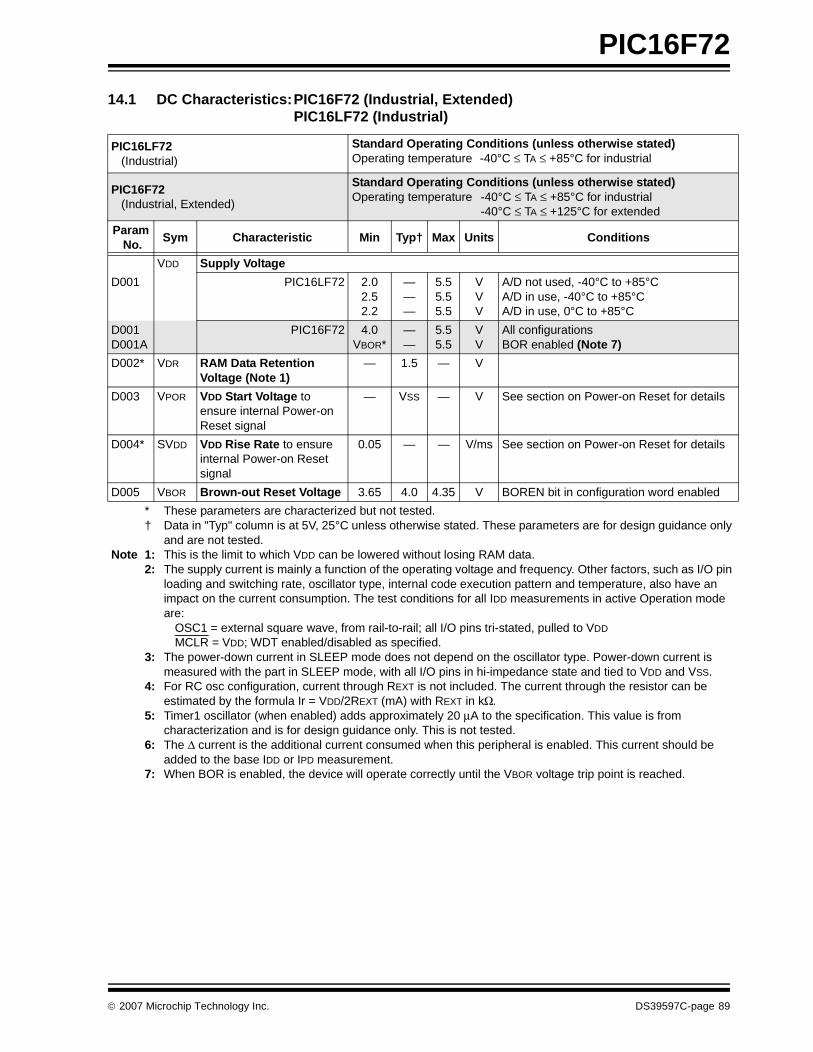
PIC16F72
14.1 DC Characteristics:PIC16F72 (Industrial, Extended) PIC16LF72 (Industrial)
PIC16LF72 (Industrial)
Standard Operating Conditions (unless otherwise stated)Operating temperature -40°C ≤ TA ≤ +85°C for industrial
PIC16F72 (Industrial, Extended)
Standard Operating Conditions (unless otherwise stated)Operating temperature -40°C ≤ TA ≤ +85°C for industrial
-40°C ≤ TA ≤ +125°C for extended
Param No.
Sym Characteristic Min Typ† Max Units Conditions
VDD Supply Voltage
D001 PIC16LF72 2.02.52.2
———
5.55.55.5
VVV
A/D not used, -40°C to +85°CA/D in use, -40°C to +85°CA/D in use, 0°C to +85°C
D001D001A
PIC16F72 4.0VBOR*
——
5.55.5
VV
All configurationsBOR enabled (Note 7)
D002* VDR RAM Data RetentionVoltage (Note 1)
— 1.5 — V
D003 VPOR VDD Start Voltage toensure internal Power-on Reset signal
— VSS — V See section on Power-on Reset for details
D004* SVDD VDD Rise Rate to ensure internal Power-on Reset signal
0.05 — — V/ms See section on Power-on Reset for details
D005 VBOR Brown-out Reset Voltage 3.65 4.0 4.35 V BOREN bit in configuration word enabled
* These parameters are characterized but not tested.† Data in "Typ" column is at 5V, 25°C unless otherwise stated. These parameters are for design guidance only
and are not tested.Note 1: This is the limit to which VDD can be lowered without losing RAM data.
2: The supply current is mainly a function of the operating voltage and frequency. Other factors, such as I/O pin loading and switching rate, oscillator type, internal code execution pattern and temperature, also have an impact on the current consumption. The test conditions for all IDD measurements in active Operation mode are:
OSC1 = external square wave, from rail-to-rail; all I/O pins tri-stated, pulled to VDD MCLR = VDD; WDT enabled/disabled as specified.
3: The power-down current in SLEEP mode does not depend on the oscillator type. Power-down current is measured with the part in SLEEP mode, with all I/O pins in hi-impedance state and tied to VDD and VSS.
4: For RC osc configuration, current through REXT is not included. The current through the resistor can be estimated by the formula Ir = VDD/2REXT (mA) with REXT in kΩ.
5: Timer1 oscillator (when enabled) adds approximately 20 μA to the specification. This value is from characterization and is for design guidance only. This is not tested.
6: The Δ current is the additional current consumed when this peripheral is enabled. This current should be added to the base IDD or IPD measurement.
7: When BOR is enabled, the device will operate correctly until the VBOR voltage trip point is reached.
© 2007 Microchip Technology Inc. DS39597C-page 89
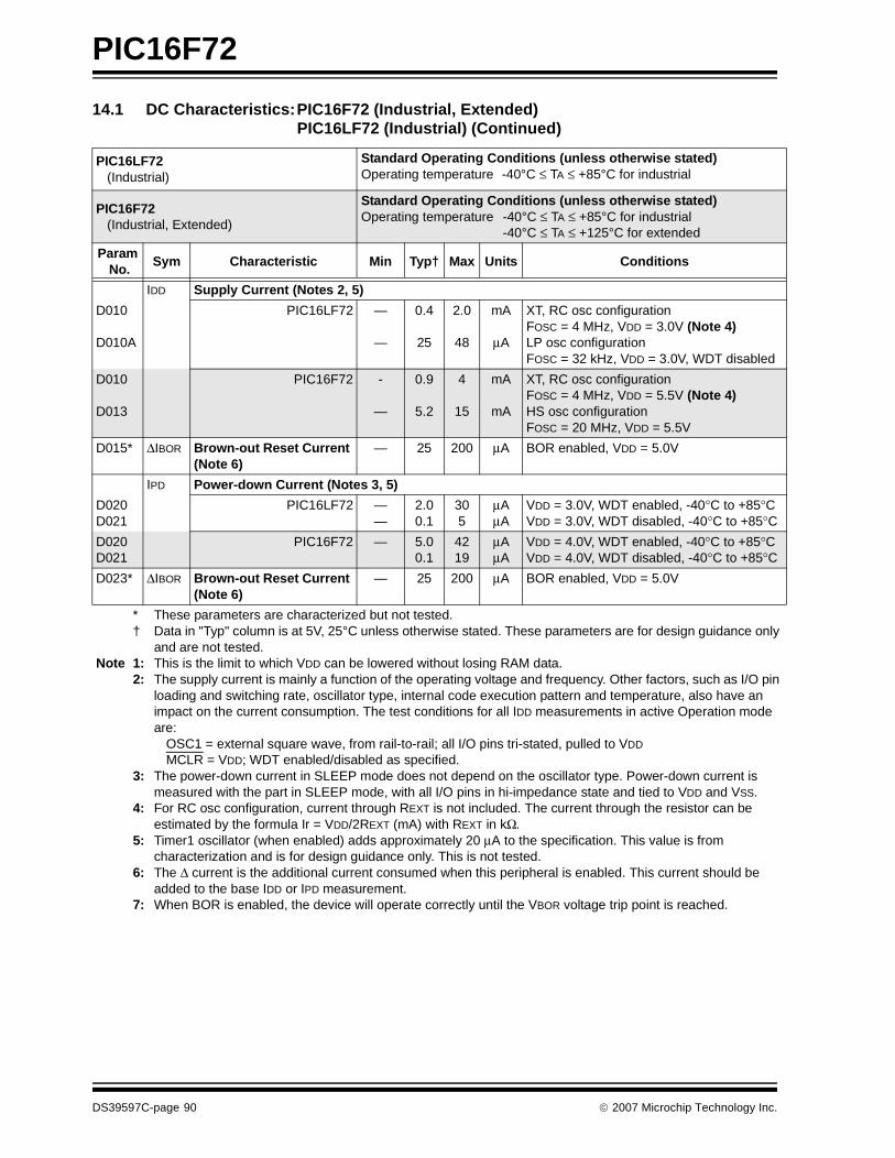
PIC16F72
IDD Supply Current (Notes 2, 5)
D010
D010A
PIC16LF72 —
—
0.4
25
2.0
48
mA
μA
XT, RC osc configurationFOSC = 4 MHz, VDD = 3.0V (Note 4)LP osc configurationFOSC = 32 kHz, VDD = 3.0V, WDT disabled
D010
D013
PIC16F72 -
—
0.9
5.2
4
15
mA
mA
XT, RC osc configuration FOSC = 4 MHz, VDD = 5.5V (Note 4)HS osc configuration FOSC = 20 MHz, VDD = 5.5V
D015* ΔIBOR Brown-out Reset Current (Note 6)
— 25 200 μA BOR enabled, VDD = 5.0V
IPD Power-down Current (Notes 3, 5)
D020D021
PIC16LF72 ——
2.00.1
305
μAμA
VDD = 3.0V, WDT enabled, -40°C to +85°CVDD = 3.0V, WDT disabled, -40°C to +85°C
D020D021
PIC16F72 — 5.00.1
4219
μAμA
VDD = 4.0V, WDT enabled, -40°C to +85°CVDD = 4.0V, WDT disabled, -40°C to +85°C
D023* ΔIBOR Brown-out Reset Current (Note 6)
— 25 200 μA BOR enabled, VDD = 5.0V
14.1 DC Characteristics:PIC16F72 (Industrial, Extended) PIC16LF72 (Industrial) (Continued)
PIC16LF72 (Industrial)
Standard Operating Conditions (unless otherwise stated)Operating temperature -40°C ≤ TA ≤ +85°C for industrial
PIC16F72 (Industrial, Extended)
Standard Operating Conditions (unless otherwise stated)Operating temperature -40°C ≤ TA ≤ +85°C for industrial
-40°C ≤ TA ≤ +125°C for extended
Param No.
Sym Characteristic Min Typ† Max Units Conditions
* These parameters are characterized but not tested.† Data in "Typ" column is at 5V, 25°C unless otherwise stated. These parameters are for design guidance only
and are not tested.Note 1: This is the limit to which VDD can be lowered without losing RAM data.
2: The supply current is mainly a function of the operating voltage and frequency. Other factors, such as I/O pin loading and switching rate, oscillator type, internal code execution pattern and temperature, also have an impact on the current consumption. The test conditions for all IDD measurements in active Operation mode are:
OSC1 = external square wave, from rail-to-rail; all I/O pins tri-stated, pulled to VDD MCLR = VDD; WDT enabled/disabled as specified.
3: The power-down current in SLEEP mode does not depend on the oscillator type. Power-down current is measured with the part in SLEEP mode, with all I/O pins in hi-impedance state and tied to VDD and VSS.
4: For RC osc configuration, current through REXT is not included. The current through the resistor can be estimated by the formula Ir = VDD/2REXT (mA) with REXT in kΩ.
5: Timer1 oscillator (when enabled) adds approximately 20 μA to the specification. This value is from characterization and is for design guidance only. This is not tested.
6: The Δ current is the additional current consumed when this peripheral is enabled. This current should be added to the base IDD or IPD measurement.
7: When BOR is enabled, the device will operate correctly until the VBOR voltage trip point is reached.
DS39597C-page 90 © 2007 Microchip Technology Inc.

PIC16F72
14.2 DC Characteristics: PIC16F72 (Industrial, Extended)PIC16LF72 (Industrial)
DC CHARACTERISTICS
Standard Operating Conditions (unless otherwise stated)Operating temperature -40°C ≤ TA ≤ +85°C for industrial
-40°C ≤ TA ≤ +125°C for extendedOperating voltage VDD range as described in DC Specification, Section 14.1.
ParamNo.
Sym Characteristic Min Typ† Max Units Conditions
VIL Input Low VoltageI/O ports
D030 with TTL buffer VSS — 0.15 VDD V For entire VDD rangeD030A VSS — 0.8V V 4.5V ≤ VDD ≤ 5.5VD031 with Schmitt Trigger buffer VSS — 0.2 VDD V
D032 MCLR, OSC1 (in RC mode) VSS — 0.2 VDD VD033 OSC1 (in XT and LP mode) VSS — 0.3V V (Note 1)
OSC1 (in HS mode) VSS — 0.3 VDD V (Note 1)VIH Input High Voltage
I/O portsD040 with TTL buffer 2.0 — VDD V 4.5V ≤ VDD ≤ 5.5VD040A 0.25 VDD + 0.8V — VDD V For entire VDD rangeD041 with Schmitt Trigger buffer 0.8 VDD — VDD V For entire VDD range
D042 MCLR 0.8 VDD — VDD VD042A OSC1 (in XT and LP mode) 1.6V — VDD V (Note 1)
OSC1 (in HS mode) 0.7 VDD — VDD V (Note 1)D043 OSC1 (in RC mode) 0.9 VDD — VDD VD070 IPURB PORTB Weak Pull-up Current 50 250 400 μA VDD = 5V, VPIN = VSS
IIL Input Leakage Current (Notes 2, 3)D060 I/O ports — — ±1 μA Vss ≤ VPIN ≤ VDD, Pin at
hi-impedance
D061 MCLR, RA4/T0CKI — — ±5 μA Vss ≤ VPIN ≤ VDD
D063 OSC1 — — ±5 μA Vss ≤ VPIN ≤ VDD, XT, HS and LP osc configuration
* These parameters are characterized but not tested.† Data in "Typ" column is at 5V, 25°C unless otherwise stated. These parameters are for design guidance only
and are not tested.Note 1: In RC oscillator configuration, the OSC1/CLKI pin is a Schmitt Trigger input. It is not recommended that the
PIC16F72 be driven with external clock in RC mode.2: The leakage current on the MCLR pin is strongly dependent on the applied voltage level. The specified levels
represent normal operating conditions. Higher leakage current may be measured at different input voltages.3: Negative current is defined as current sourced by the pin.
© 2007 Microchip Technology Inc. DS39597C-page 91
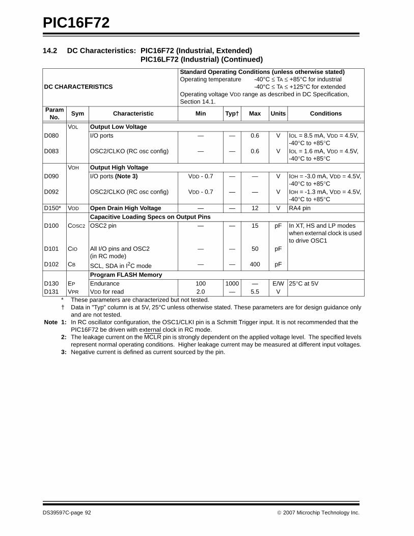
PIC16F72
VOL Output Low VoltageD080 I/O ports — — 0.6 V IOL = 8.5 mA, VDD = 4.5V,
-40°C to +85°CD083 OSC2/CLKO (RC osc config) — — 0.6 V IOL = 1.6 mA, VDD = 4.5V,
-40°C to +85°CVOH Output High Voltage
D090 I/O ports (Note 3) VDD - 0.7 — — V IOH = -3.0 mA, VDD = 4.5V, -40°C to +85°C
D092 OSC2/CLKO (RC osc config) VDD - 0.7 — — V IOH = -1.3 mA, VDD = 4.5V, -40°C to +85°C
D150* VOD Open Drain High Voltage — — 12 V RA4 pinCapacitive Loading Specs on Output Pins
D100 COSC2 OSC2 pin — — 15 pF In XT, HS and LP modes when external clock is used to drive OSC1
D101 CIO All I/O pins and OSC2(in RC mode)
— — 50 pF
D102 CB SCL, SDA in I2C mode — — 400 pF
Program FLASH MemoryD130 EP Endurance 100 1000 — E/W 25°C at 5VD131 VPR VDD for read 2.0 — 5.5 V
14.2 DC Characteristics: PIC16F72 (Industrial, Extended)PIC16LF72 (Industrial) (Continued)
DC CHARACTERISTICS
Standard Operating Conditions (unless otherwise stated)Operating temperature -40°C ≤ TA ≤ +85°C for industrial
-40°C ≤ TA ≤ +125°C for extendedOperating voltage VDD range as described in DC Specification, Section 14.1.
ParamNo.
Sym Characteristic Min Typ† Max Units Conditions
* These parameters are characterized but not tested.† Data in "Typ" column is at 5V, 25°C unless otherwise stated. These parameters are for design guidance only
and are not tested.Note 1: In RC oscillator configuration, the OSC1/CLKI pin is a Schmitt Trigger input. It is not recommended that the
PIC16F72 be driven with external clock in RC mode.2: The leakage current on the MCLR pin is strongly dependent on the applied voltage level. The specified levels
represent normal operating conditions. Higher leakage current may be measured at different input voltages.3: Negative current is defined as current sourced by the pin.
DS39597C-page 92 © 2007 Microchip Technology Inc.
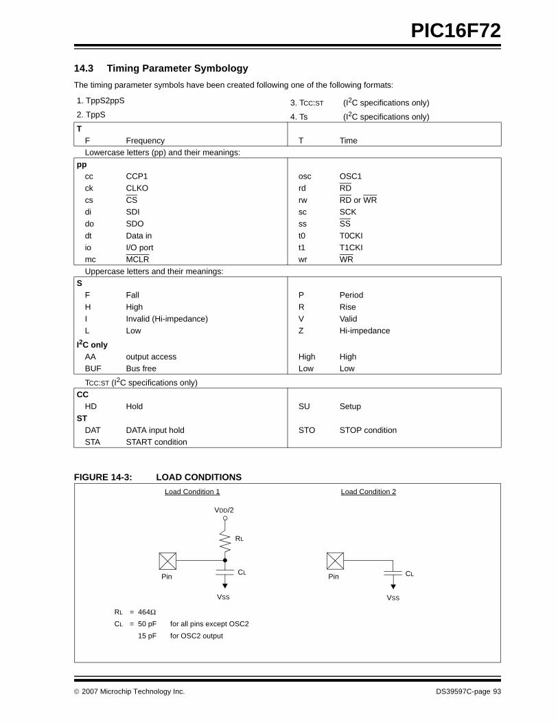
PIC16F72
14.3 Timing Parameter Symbology
The timing parameter symbols have been created following one of the following formats:
FIGURE 14-3: LOAD CONDITIONS
1. TppS2ppS 3. TCC:ST (I2C specifications only)2. TppS 4. Ts (I2C specifications only)
TF Frequency T TimeLowercase letters (pp) and their meanings:
ppcc CCP1 osc OSC1ck CLKO rd RD
cs CS rw RD or WRdi SDI sc SCKdo SDO ss SS
dt Data in t0 T0CKIio I/O port t1 T1CKImc MCLR wr WR
Uppercase letters and their meanings:S
F Fall P Period
H High R RiseI Invalid (Hi-impedance) V ValidL Low Z Hi-impedance
I2C onlyAA output access High HighBUF Bus free Low Low
TCC:ST (I2C specifications only)CC
HD Hold SU Setup
STDAT DATA input hold STO STOP conditionSTA START condition
VDD/2
CL
RL
Pin Pin
VSS VSS
CL
RL = 464Ω
CL = 50 pF for all pins except OSC2
15 pF for OSC2 output
Load Condition 1 Load Condition 2
© 2007 Microchip Technology Inc. DS39597C-page 93
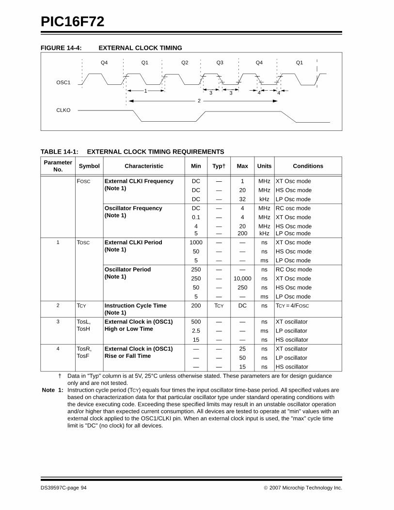
PIC16F72
FIGURE 14-4: EXTERNAL CLOCK TIMING
TABLE 14-1: EXTERNAL CLOCK TIMING REQUIREMENTS
OSC1
CLKO
Q4 Q1 Q2 Q3 Q4 Q1
1
2
3 3 4 4
Parameter No.
Symbol Characteristic Min Typ† Max Units Conditions
FOSC External CLKI Frequency (Note 1)
DC — 1 MHz XT Osc mode
DC — 20 MHz HS Osc mode
DC — 32 kHz LP Osc mode
Oscillator Frequency (Note 1)
DC — 4 MHz RC osc mode
0.1 — 4 MHz XT Osc mode
45
——
20200
MHzkHz
HS Osc mode LP Osc mode
1 TOSC External CLKI Period(Note 1)
1000 — — ns XT Osc mode
50 — — ns HS Osc mode
5 — — ms LP Osc mode
Oscillator Period(Note 1)
250 — — ns RC Osc mode
250 — 10,000 ns XT Osc mode
50 — 250 ns HS Osc mode
5 — — ms LP Osc mode
2 TCY Instruction Cycle Time (Note 1)
200 TCY DC ns TCY = 4/FOSC
3 TosL,TosH
External Clock in (OSC1) High or Low Time
500 — — ns XT oscillator
2.5 — — ms LP oscillator
15 — — ns HS oscillator
4 TosR,TosF
External Clock in (OSC1) Rise or Fall Time
— — 25 ns XT oscillator
— — 50 ns LP oscillator
— — 15 ns HS oscillator
† Data in "Typ" column is at 5V, 25°C unless otherwise stated. These parameters are for design guidance only and are not tested.
Note 1: Instruction cycle period (TCY) equals four times the input oscillator time-base period. All specified values are based on characterization data for that particular oscillator type under standard operating conditions with the device executing code. Exceeding these specified limits may result in an unstable oscillator operation and/or higher than expected current consumption. All devices are tested to operate at "min" values with an external clock applied to the OSC1/CLKI pin. When an external clock input is used, the "max" cycle time limit is "DC" (no clock) for all devices.
DS39597C-page 94 © 2007 Microchip Technology Inc.
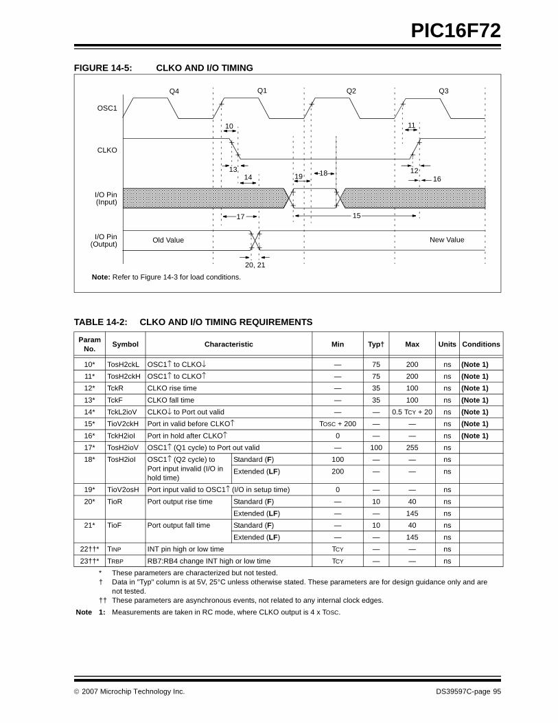
PIC16F72
FIGURE 14-5: CLKO AND I/O TIMING
TABLE 14-2: CLKO AND I/O TIMING REQUIREMENTS
Note: Refer to Figure 14-3 for load conditions.
OSC1
CLKO
I/O Pin(Input)
I/O Pin(Output)
Q4 Q1 Q2 Q3
10
1314
17
20, 21
19 18
15
11
1216
Old Value New Value
ParamNo.
Symbol Characteristic Min Typ† Max Units Conditions
10* TosH2ckL OSC1↑ to CLKO↓ — 75 200 ns (Note 1)
11* TosH2ckH OSC1↑ to CLKO↑ — 75 200 ns (Note 1)
12* TckR CLKO rise time — 35 100 ns (Note 1)
13* TckF CLKO fall time — 35 100 ns (Note 1)
14* TckL2ioV CLKO↓ to Port out valid — — 0.5 TCY + 20 ns (Note 1)
15* TioV2ckH Port in valid before CLKO↑ TOSC + 200 — — ns (Note 1)
16* TckH2ioI Port in hold after CLKO↑ 0 — — ns (Note 1)
17* TosH2ioV OSC1↑ (Q1 cycle) to Port out valid — 100 255 ns
18* TosH2ioI OSC1↑ (Q2 cycle) to Port input invalid (I/O in hold time)
Standard (F) 100 — — ns
Extended (LF) 200 — — ns
19* TioV2osH Port input valid to OSC1↑ (I/O in setup time) 0 — — ns
20* TioR Port output rise time Standard (F) — 10 40 ns
Extended (LF) — — 145 ns
21* TioF Port output fall time Standard (F) — 10 40 ns
Extended (LF) — — 145 ns
22††* TINP INT pin high or low time TCY — — ns
23††* TRBP RB7:RB4 change INT high or low time TCY — — ns
* These parameters are characterized but not tested.† Data in "Typ" column is at 5V, 25°C unless otherwise stated. These parameters are for design guidance only and are
not tested.†† These parameters are asynchronous events, not related to any internal clock edges.
Note 1: Measurements are taken in RC mode, where CLKO output is 4 x TOSC.
© 2007 Microchip Technology Inc. DS39597C-page 95
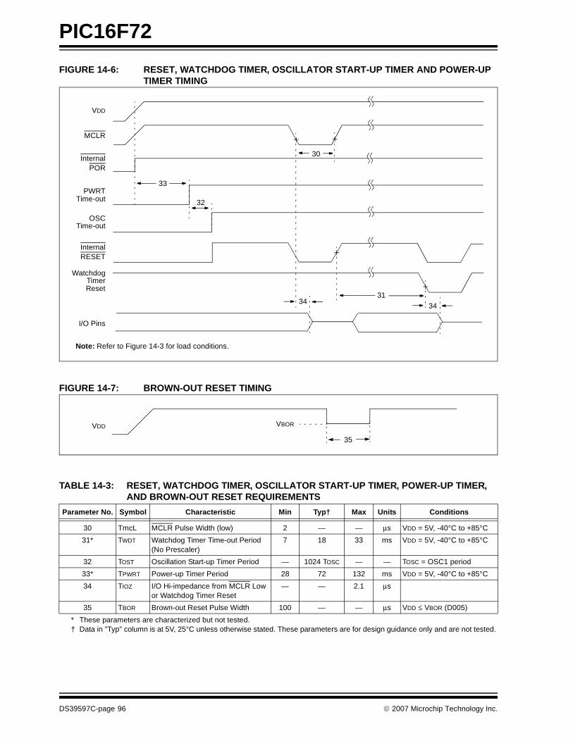
PIC16F72
FIGURE 14-6: RESET, WATCHDOG TIMER, OSCILLATOR START-UP TIMER AND POWER-UP TIMER TIMING
FIGURE 14-7: BROWN-OUT RESET TIMING
TABLE 14-3: RESET, WATCHDOG TIMER, OSCILLATOR START-UP TIMER, POWER-UP TIMER, AND BROWN-OUT RESET REQUIREMENTS
VDD
MCLR
InternalPOR
PWRTTime-out
OSCTime-out
InternalRESET
WatchdogTimerReset
33
32
30
3134
I/O Pins
34
Note: Refer to Figure 14-3 for load conditions.
VDD VBOR
35
Parameter No. Symbol Characteristic Min Typ† Max Units Conditions
30 TmcL MCLR Pulse Width (low) 2 — — μs VDD = 5V, -40°C to +85°C
31* TWDT Watchdog Timer Time-out Period (No Prescaler)
7 18 33 ms VDD = 5V, -40°C to +85°C
32 TOST Oscillation Start-up Timer Period — 1024 TOSC — — TOSC = OSC1 period
33* TPWRT Power-up Timer Period 28 72 132 ms VDD = 5V, -40°C to +85°C
34 TIOZ I/O Hi-impedance from MCLR Low or Watchdog Timer Reset
— — 2.1 μs
35 TBOR Brown-out Reset Pulse Width 100 — — μs VDD ≤ VBOR (D005)
* These parameters are characterized but not tested.† Data in "Typ" column is at 5V, 25°C unless otherwise stated. These parameters are for design guidance only and are not tested.
DS39597C-page 96 © 2007 Microchip Technology Inc.
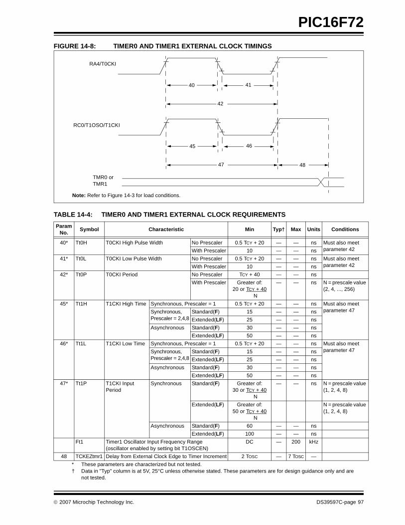
PIC16F72
FIGURE 14-8: TIMER0 AND TIMER1 EXTERNAL CLOCK TIMINGSTABLE 14-4: TIMER0 AND TIMER1 EXTERNAL CLOCK REQUIREMENTS
Param No.
Symbol Characteristic Min Typ† Max Units Conditions
40* Tt0H T0CKI High Pulse Width No Prescaler 0.5 TCY + 20 — — ns Must also meet parameter 42 With Prescaler 10 — — ns
41* Tt0L T0CKI Low Pulse Width No Prescaler 0.5 TCY + 20 — — ns Must also meet parameter 42 With Prescaler 10 — — ns
42* Tt0P T0CKI Period No Prescaler TCY + 40 — — ns
With Prescaler Greater of:20 or TCY + 40
N
— — ns N = prescale value (2, 4, ..., 256)
45* Tt1H T1CKI High Time Synchronous, Prescaler = 1 0.5 TCY + 20 — — ns Must also meet parameter 47 Synchronous,
Prescaler = 2,4,8Standard(F) 15 — — ns
Extended(LF) 25 — — ns
Asynchronous Standard(F) 30 — — ns
Extended(LF) 50 — — ns
46* Tt1L T1CKI Low Time Synchronous, Prescaler = 1 0.5 TCY + 20 — — ns Must also meet parameter 47 Synchronous,
Prescaler = 2,4,8Standard(F) 15 — — ns
Extended(LF) 25 — — ns
Asynchronous Standard(F) 30 — — ns
Extended(LF) 50 — — ns
47* Tt1P T1CKI Input Period
Synchronous Standard(F) Greater of:30 or TCY + 40
N
— — ns N = prescale value (1, 2, 4, 8)
Extended(LF) Greater of:50 or TCY + 40
N
N = prescale value (1, 2, 4, 8)
Asynchronous Standard(F) 60 — — ns
Extended(LF) 100 — — ns
Ft1 Timer1 Oscillator Input Frequency Range (oscillator enabled by setting bit T1OSCEN)
DC — 200 kHz
48 TCKEZtmr1 Delay from External Clock Edge to Timer Increment 2 TOSC — 7 TOSC —
* These parameters are characterized but not tested.† Data in "Typ" column is at 5V, 25°C unless otherwise stated. These parameters are for design guidance only and are
not tested.
Note: Refer to Figure 14-3 for load conditions.
46
47
45
48
41
42
40
RA4/T0CKI
RC0/T1OSO/T1CKI
TMR0 orTMR1
© 2007 Microchip Technology Inc. DS39597C-page 97
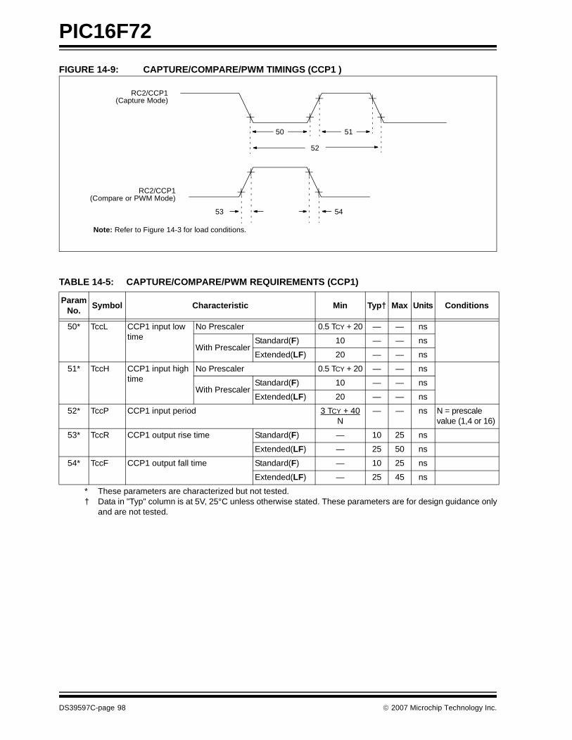
PIC16F72
FIGURE 14-9: CAPTURE/COMPARE/PWM TIMINGS (CCP1 )
TABLE 14-5: CAPTURE/COMPARE/PWM REQUIREMENTS (CCP1)
Note: Refer to Figure 14-3 for load conditions.
RC2/CCP1(Capture Mode)
50 51
52
53 54
RC2/CCP1(Compare or PWM Mode)
Param No.
Symbol Characteristic Min Typ† Max Units Conditions
50* TccL CCP1 input low time
No Prescaler 0.5 TCY + 20 — — ns
With PrescalerStandard(F) 10 — — ns
Extended(LF) 20 — — ns
51* TccH CCP1 input high time
No Prescaler 0.5 TCY + 20 — — ns
With PrescalerStandard(F) 10 — — ns
Extended(LF) 20 — — ns
52* TccP CCP1 input period 3 TCY + 40N
— — ns N = prescale value (1,4 or 16)
53* TccR CCP1 output rise time Standard(F) — 10 25 ns
Extended(LF) — 25 50 ns
54* TccF CCP1 output fall time Standard(F) — 10 25 ns
Extended(LF) — 25 45 ns
* These parameters are characterized but not tested.† Data in "Typ" column is at 5V, 25°C unless otherwise stated. These parameters are for design guidance only
and are not tested.
DS39597C-page 98 © 2007 Microchip Technology Inc.
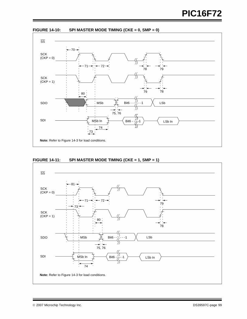
PIC16F72
FIGURE 14-10: SPI MASTER MODE TIMING (CKE = 0, SMP = 0)
FIGURE 14-11: SPI MASTER MODE TIMING (CKE = 1, SMP = 1)
SS
SCK(CKP = 0)
SCK(CKP = 1)
SDO
SDI
70
71 72
7374
75, 76
787980
7978
MSb LSbBit6 - - - - - -1
MSb In LSb InBit6 - - - -1
Note: Refer to Figure 14-3 for load conditions.
SS
SCK(CKP = 0)
SCK(CKP = 1)
SDO
SDI
81
71 72
74
75, 76
78
80
MSb
7973
MSb In
Bit6 - - - - - -1
LSb InBit6 - - - -1
LSb
Note: Refer to Figure 14-3 for load conditions.
© 2007 Microchip Technology Inc. DS39597C-page 99

PIC16F72
FIGURE 14-12: SPI SLAVE MODE TIMING (CKE = 0)
FIGURE 14-13: SPI SLAVE MODE TIMING (CKE = 1)
SS
SCK(CKP = 0)
SCK(CKP = 1)
SDO
SDI
70
71 72
7374
75, 76 77
787980
7978
MSb LSbBit6 - - - - - -1
MSb In Bit6 - - - -1 LSb In
83
Note: Refer to Figure 14-3 for load conditions.
SS
SCK(CKP = 0)
SCK(CKP = 1)
SDO
SDI
70
71 72
82
SDI
74
75, 76
MSb Bit6 - - - - - -1 LSb
77
MSb In Bit6 - - - -1 LSb In
80
83
Note: Refer to Figure 14-3 for load conditions.
DS39597C-page 100 © 2007 Microchip Technology Inc.
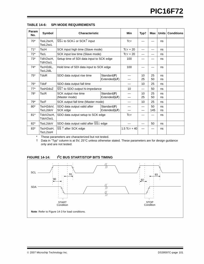
PIC16F72
TABLE 14-6: SPI MODE REQUIREMENTS
FIGURE 14-14: I2C BUS START/STOP BITS TIMING
Param No.
Symbol Characteristic Min Typ† Max Units Conditions
70* TssL2scH, TssL2scL
SS↓ to SCK↓ or SCK↑ input TCY — — ns
71* TscH SCK input high time (Slave mode) TCY + 20 — — ns
72* TscL SCK input low time (Slave mode) TCY + 20 — — ns
73* TdiV2scH, TdiV2scL
Setup time of SDI data input to SCK edge 100 — — ns
74* TscH2diL, TscL2diL
Hold time of SDI data input to SCK edge 100 — — ns
75* TdoR SDO data output rise time Standard(F)Extended(LF)
——
1025
2550
nsns
76* TdoF SDO data output fall time — 10 25 ns
77* TssH2doZ SS↑ to SDO output hi-impedance 10 — 50 ns
78* TscR SCK output rise time (Master mode)
Standard(F)Extended(LF)
——
1025
2550
nsns
79* TscF SCK output fall time (Master mode) — 10 25 ns
80* TscH2doV,TscL2doV
SDO data output valid after SCK edge
Standard(F)Extended(LF)
——
——
50145
nsns
81* TdoV2scH,TdoV2scL
SDO data output setup to SCK edge TCY — — ns
82* TssL2doV SDO data output valid after SS↓ edge — — 50 ns
83* TscH2ssH,TscL2ssH
SS ↑ after SCK edge 1.5 TCY + 40 — — ns
* These parameters are characterized but not tested.† Data in "Typ" column is at 5V, 25°C unless otherwise stated. These parameters are for design guidance
only and are not tested.
Note: Refer to Figure 14-3 for load conditions.
91
92
93SCL
SDA
STARTCondition
STOPCondition
90
© 2007 Microchip Technology Inc. DS39597C-page 101
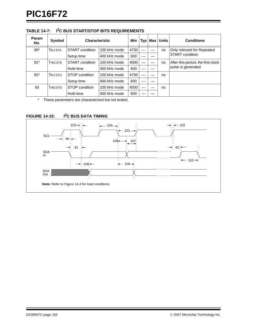
PIC16F72
TABLE 14-7: I2C BUS START/STOP BITS REQUIREMENTS
FIGURE 14-15: I2C BUS DATA TIMING
ParamNo.
Symbol Characteristic Min Typ Max Units Conditions
90* TSU:STA START condition 100 kHz mode 4700 — — ns Only relevant for Repeated START conditionSetup time 400 kHz mode 600 — —
91* THD:STA START condition 100 kHz mode 4000 — — ns After this period, the first clock pulse is generatedHold time 400 kHz mode 600 — —
92* TSU:STO STOP condition 100 kHz mode 4700 — — ns
Setup time 400 kHz mode 600 — —
93 THD:STO STOP condition 100 kHz mode 4000 — — ns
Hold time 400 kHz mode 600 — —
* These parameters are characterized but not tested.
Note: Refer to Figure 14-3 for load conditions.
90
91 92
100
101
103
106 107
109 109110
102
SCL
SDAIn
SDAOut
DS39597C-page 102 © 2007 Microchip Technology Inc.
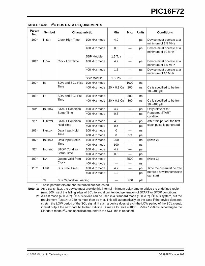
PIC16F72
TABLE 14-8: I2C BUS DATA REQUIREMENTS
ParamNo.
Symbol Characteristic Min Max Units Conditions
100* THIGH Clock High Time 100 kHz mode 4.0 — μs Device must operate at a minimum of 1.5 MHz
400 kHz mode 0.6 — μs Device must operate at a minimum of 10 MHz
SSP Module 1.5 TCY —
101* TLOW Clock Low Time 100 kHz mode 4.7 — μs Device must operate at a minimum of 1.5 MHz
400 kHz mode 1.3 — μs Device must operate at a minimum of 10 MHz
SSP Module 1.5 TCY —
102* TR SDA and SCL Rise Time
100 kHz mode — 1000 ns
400 kHz mode 20 + 0.1 CB 300 ns CB is specified to be from 10 - 400 pF
103* TF SDA and SCL Fall Time
100 kHz mode — 300 ns
400 kHz mode 20 + 0.1 CB 300 ns CB is specified to be from 10 - 400 pF
90* TSU:STA START Condition Setup Time
100 kHz mode 4.7 — μs Only relevant for Repeated START condition
400 kHz mode 0.6 — μs
91* THD:STA START Condition Hold Time
100 kHz mode 4.0 — μs After this period, the first clock pulse is generated400 kHz mode 0.6 — μs
106* THD:DAT Data Input Hold Time
100 kHz mode 0 — ns
400 kHz mode 0 0.9 μs
107* TSU:DAT Data Input Setup Time
100 kHz mode 250 — ns (Note 2)
400 kHz mode 100 — ns
92* TSU:STO STOP Condition Setup Time
100 kHz mode 4.7 — μs
400 kHz mode 0.6 — μs
109* TAA Output Valid from Clock
100 kHz mode — 3500 ns (Note 1)
400 kHz mode — — ns
110* TBUF Bus Free Time 100 kHz mode 4.7 — μs Time the bus must be free before a new transmission can start
400 kHz mode 1.3 — μs
CB Bus Capacitive Loading — 400 pF
* These parameters are characterized but not tested.Note 1: As a transmitter, the device must provide this internal minimum delay time to bridge the undefined region
(min. 300 ns) of the falling edge of SCL to avoid unintended generation of START or STOP conditions.2: A Fast mode (400 kHz) I2C bus device can be used in a Standard mode (100 kHz) I2C bus system, but the
requirement TSU:DAT ≥ 250 ns must then be met. This will automatically be the case if the device does not stretch the LOW period of the SCL signal. If such a device does stretch the LOW period of the SCL signal, it must output the next data bit to the SDA line TR max.+TSU:DAT = 1000 + 250 = 1250 ns (according to the Standard mode I2C bus specification), before the SCL line is released.
© 2007 Microchip Technology Inc. DS39597C-page 103
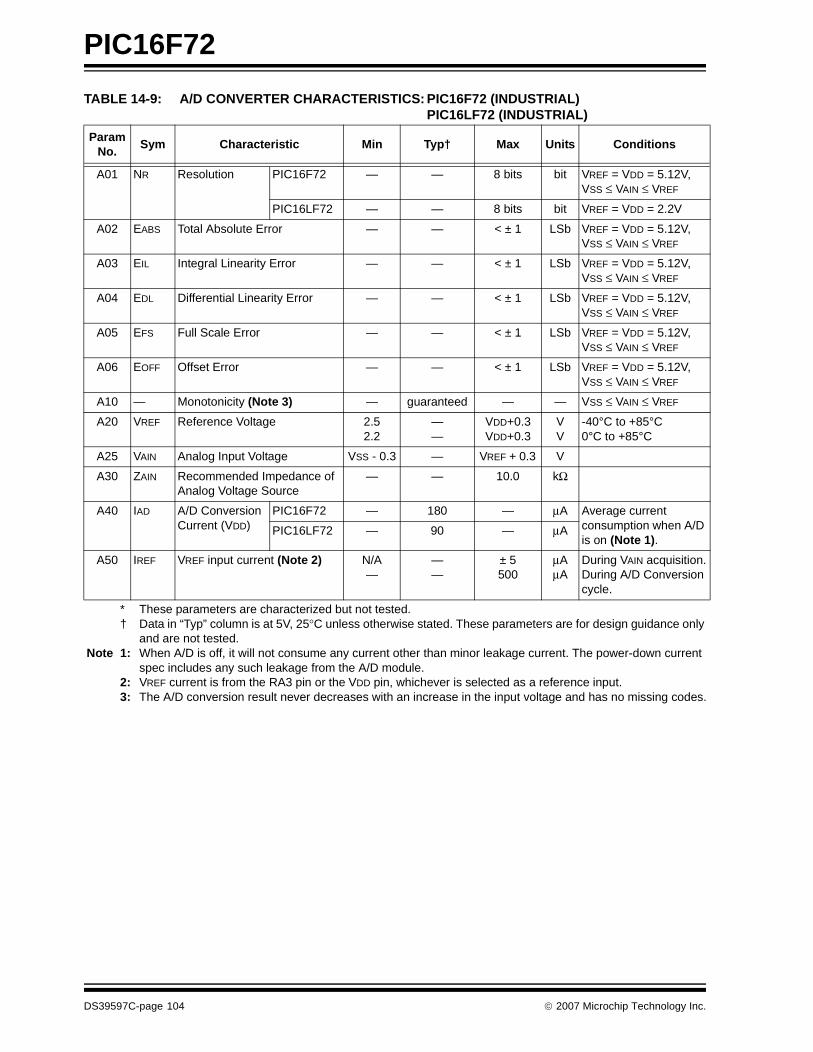
PIC16F72
TABLE 14-9: A/D CONVERTER CHARACTERISTICS: PIC16F72 (INDUSTRIAL)PIC16LF72 (INDUSTRIAL)
ParamNo.
Sym Characteristic Min Typ† Max Units Conditions
A01 NR Resolution PIC16F72 — — 8 bits bit VREF = VDD = 5.12V, VSS ≤ VAIN ≤ VREF
PIC16LF72 — — 8 bits bit VREF = VDD = 2.2V
A02 EABS Total Absolute Error — — < ± 1 LSb VREF = VDD = 5.12V, VSS ≤ VAIN ≤ VREF
A03 EIL Integral Linearity Error — — < ± 1 LSb VREF = VDD = 5.12V, VSS ≤ VAIN ≤ VREF
A04 EDL Differential Linearity Error — — < ± 1 LSb VREF = VDD = 5.12V, VSS ≤ VAIN ≤ VREF
A05 EFS Full Scale Error — — < ± 1 LSb VREF = VDD = 5.12V, VSS ≤ VAIN ≤ VREF
A06 EOFF Offset Error — — < ± 1 LSb VREF = VDD = 5.12V, VSS ≤ VAIN ≤ VREF
A10 — Monotonicity (Note 3) — guaranteed — — VSS ≤ VAIN ≤ VREF
A20 VREF Reference Voltage 2.52.2
——
VDD+0.3VDD+0.3
VV
-40°C to +85°C0°C to +85°C
A25 VAIN Analog Input Voltage VSS - 0.3 — VREF + 0.3 V
A30 ZAIN Recommended Impedance of Analog Voltage Source
— — 10.0 kΩ
A40 IAD A/D Conversion Current (VDD)
PIC16F72 — 180 — μA Average current consumption when A/D is on (Note 1).
PIC16LF72 — 90 — μA
A50 IREF VREF input current (Note 2) N/A—
——
± 5500
μAμA
During VAIN acquisition.During A/D Conversion cycle.
* These parameters are characterized but not tested.† Data in “Typ” column is at 5V, 25°C unless otherwise stated. These parameters are for design guidance only
and are not tested.Note 1: When A/D is off, it will not consume any current other than minor leakage current. The power-down current
spec includes any such leakage from the A/D module.2: VREF current is from the RA3 pin or the VDD pin, whichever is selected as a reference input.3: The A/D conversion result never decreases with an increase in the input voltage and has no missing codes.
DS39597C-page 104 © 2007 Microchip Technology Inc.
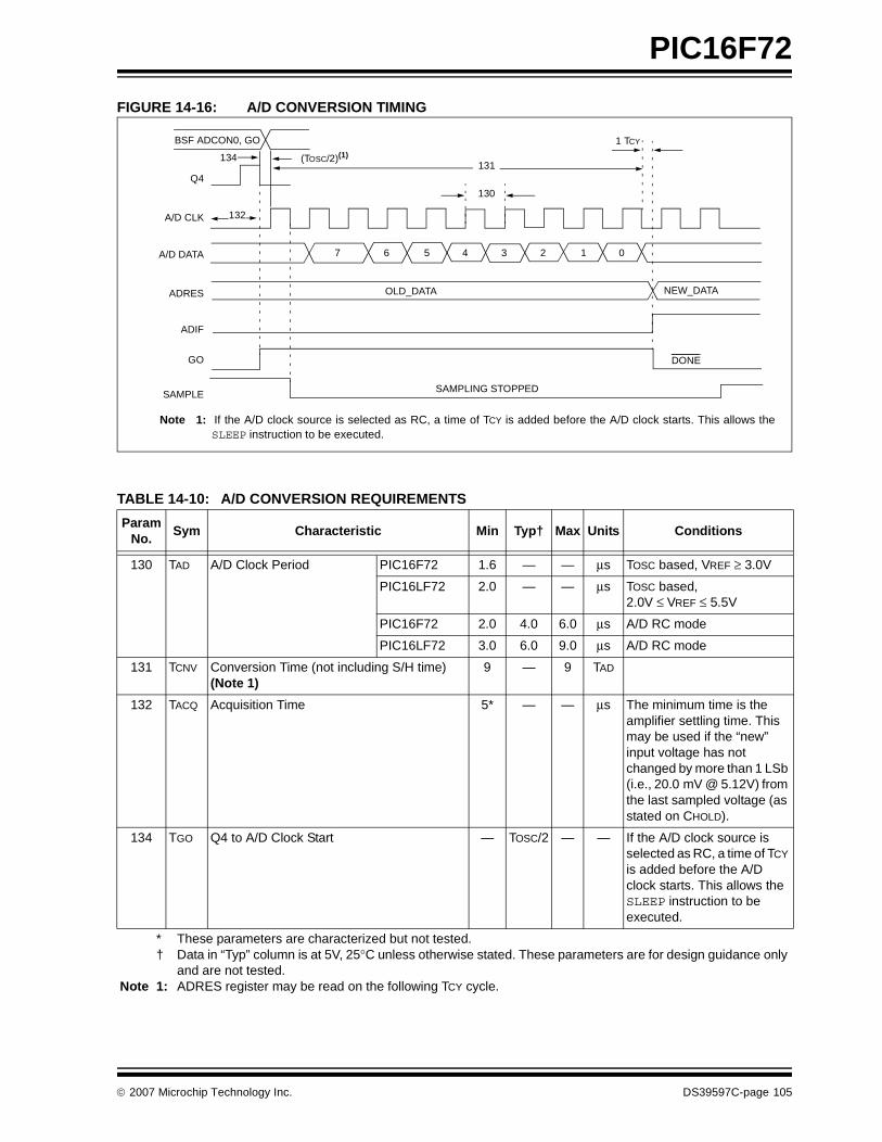
PIC16F72
FIGURE 14-16: A/D CONVERSION TIMING
TABLE 14-10: A/D CONVERSION REQUIREMENTS
131
130
132
BSF ADCON0, GO
Q4
A/D CLK
A/D DATA
ADRES
ADIF
GO
SAMPLE
OLD_DATA
SAMPLING STOPPED
DONE
NEW_DATA
(TOSC/2)(1)
7 6 5 4 3 2 1 0
Note 1: If the A/D clock source is selected as RC, a time of TCY is added before the A/D clock starts. This allows theSLEEP instruction to be executed.
1 TCY
134
Param No.
Sym Characteristic Min Typ† Max Units Conditions
130 TAD A/D Clock Period PIC16F72 1.6 — — μs TOSC based, VREF ≥ 3.0V
PIC16LF72 2.0 — — μs TOSC based, 2.0V ≤ VREF ≤ 5.5V
PIC16F72 2.0 4.0 6.0 μs A/D RC mode
PIC16LF72 3.0 6.0 9.0 μs A/D RC mode
131 TCNV Conversion Time (not including S/H time) (Note 1)
9 — 9 TAD
132 TACQ Acquisition Time 5* — — μs The minimum time is the amplifier settling time. This may be used if the “new” input voltage has not changed by more than 1 LSb (i.e., 20.0 mV @ 5.12V) from the last sampled voltage (as stated on CHOLD).
134 TGO Q4 to A/D Clock Start — TOSC/2 — — If the A/D clock source is selected as RC, a time of TCY is added before the A/D clock starts. This allows the SLEEP instruction to be executed.
* These parameters are characterized but not tested.† Data in “Typ” column is at 5V, 25°C unless otherwise stated. These parameters are for design guidance only
and are not tested.Note 1: ADRES register may be read on the following TCY cycle.
© 2007 Microchip Technology Inc. DS39597C-page 105

PIC16F72
NOTES:
DS39597C-page 106 © 2007 Microchip Technology Inc.
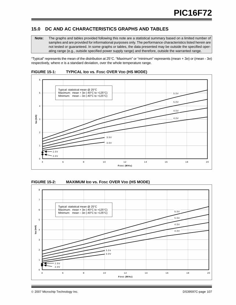
PIC16F72
15.0 DC AND AC CHARACTERISTICS GRAPHS AND TABLES
“Typical” represents the mean of the distribution at 25°C. “Maximum” or “minimum” represents (mean + 3σ) or (mean - 3σ)respectively, where σ is a standard deviation, over the whole temperature range.
FIGURE 15-1: TYPICAL IDD vs. FOSC OVER VDD (HS MODE)
FIGURE 15-2: MAXIMUM IDD vs. FOSC OVER VDD (HS MODE)
Note: The graphs and tables provided following this note are a statistical summary based on a limited number ofsamples and are provided for informational purposes only. The performance characteristics listed herein arenot tested or guaranteed. In some graphs or tables, the data presented may be outside the specified oper-ating range (e.g., outside specified power supply range) and therefore, outside the warranted range.
0
1
2
3
4
5
6
4 6 8 10 12 14 16 18 20
FO SC (M Hz)
I DD
(m
A)
5.5V
5.0V
4.5V
4.0V
3.5V
3.0V
2.5V
2.0V
Typical: statistical mean @ 25°CMaximum: mean + 3σ (-40°C to +125°C) Minimum: mean – 3σ (-40°C to +125°C)
0
1
2
3
4
5
6
7
8
4 6 8 10 12 14 16 18 20
FO S C (M Hz)
I DD
(m
A)
5.5V
5.0V
4.5V
4.0V
3.5V
3.0V
2.5V
2.0V
Typical: statistical mean @ 25°CMaximum: mean + 3σ (-40°C to +125°C) Minimum: mean – 3σ (-40°C to +125°C)
© 2007 Microchip Technology Inc. DS39597C-page 107
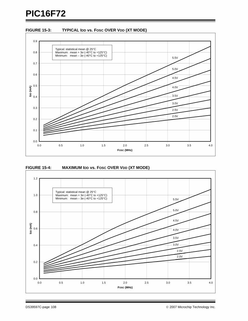
PIC16F72
FIGURE 15-3: TYPICAL IDD vs. FOSC OVER VDD (XT MODE)
FIGURE 15-4: MAXIMUM IDD vs. FOSC OVER VDD (XT MODE)
0.0
0.1
0.2
0.3
0.4
0.5
0.6
0.7
0.8
0.9
0.0 0.5 1.0 1.5 2.0 2.5 3.0 3.5 4.0
FOSC (MHz)
IDD
(m
A)
5.5V
5.0V
4.5V
4.0V
3.5V
3.0V
2.5V
2.0V
Typical: statistical mean @ 25°CMaximum: mean + 3σ (-40°C to +125°C) Minimum: mean – 3σ (-40°C to +125°C)
0.0
0.2
0.4
0.6
0.8
1.0
1.2
0.0 0.5 1.0 1.5 2.0 2.5 3.0 3.5 4.0
FOSC (MHz)
IDD
(m
A)
5.5V
5.0V
4.5V
4.0V
3.5V
3.0V
2.5V
2.0V
Typical: statistical mean @ 25°CMaximum: mean + 3σ (-40°C to +125°C) Minimum: mean – 3σ (-40°C to +125°C)
DS39597C-page 108 © 2007 Microchip Technology Inc.
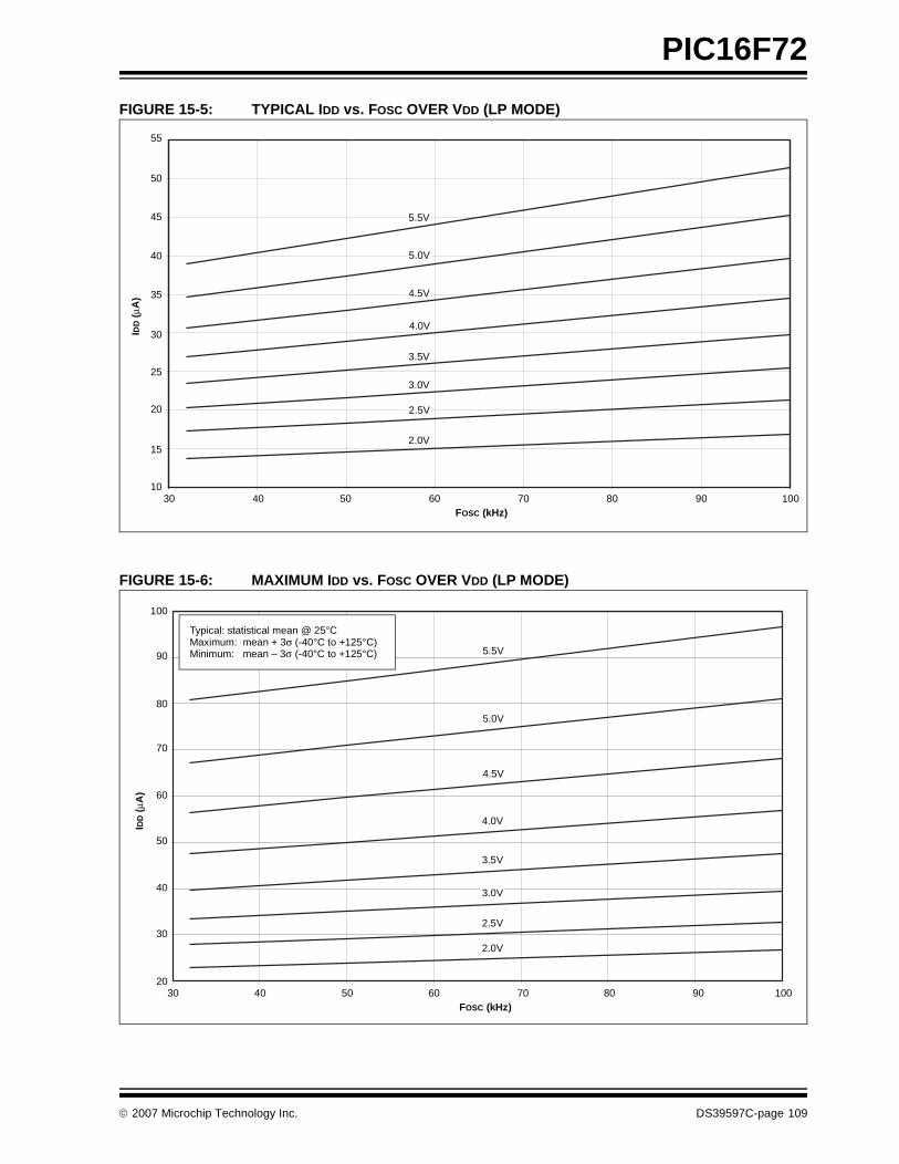
PIC16F72
FIGURE 15-5: TYPICAL IDD vs. FOSC OVER VDD (LP MODE)
FIGURE 15-6: MAXIMUM IDD vs. FOSC OVER VDD (LP MODE)
55
40
15
10
25
20
30
35
45
50
30 50 6040 70 80 90 100
IDD
(μA
)
FOSC (kHz)
3.5V
3.0V
2.0V
5.5V
5.0V
4.5V
4.0V
2.5V
Typical: statistical mean @ 25°CMaximum: mean + 3σ (-40°C to +125°C) Minimum: mean – 3σ (-40°C to +125°C)
30
2030 50 6040 70 80 90 100
IDD
(μA
)
FOSC (kHz)
40
50
60
70
80
90
100
5.5V
5.0V
4.5V
4.0V
3.5V
3.0V
2.5V
2.0V
© 2007 Microchip Technology Inc. DS39597C-page 109
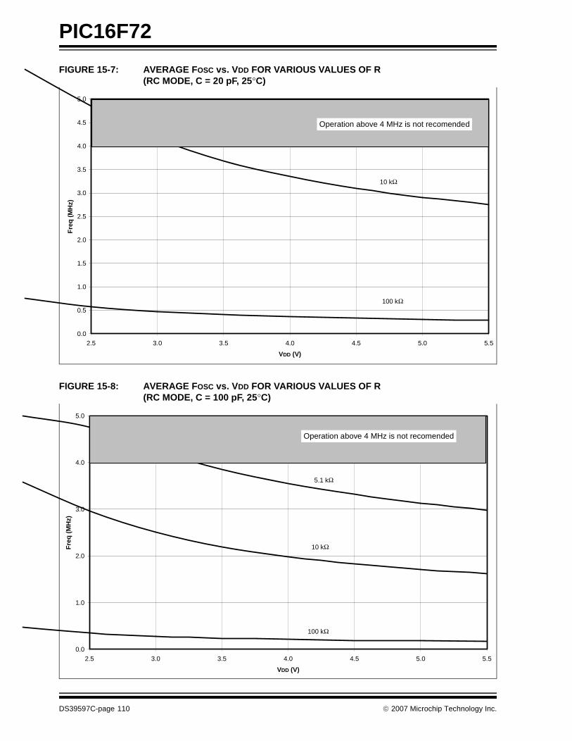
PIC16F72
FIGURE 15-7: AVERAGE FOSC vs. VDD FOR VARIOUS VALUES OF R (RC MODE, C = 20 pF, 25°C)
FIGURE 15-8: AVERAGE FOSC vs. VDD FOR VARIOUS VALUES OF R(RC MODE, C = 100 pF, 25°C)
0.0
0.5
1.0
1.5
2.0
2.5
3.0
3.5
4.0
4.5
5.0
2.5 3.0 3.5 4.0 4.5 5.0 5.5
VDD (V)
Fre
q (
MH
z)
10 kΩ
100 kΩ
Operation above 4 MHz is not recomended
0.0
1.0
2.0
3.0
4.0
5.0
2.5 3.0 3.5 4.0 4.5 5.0 5.5
VDD (V)
Fre
q (
MH
z)
5.1 kΩ
10 kΩ
100 kΩ
Operation above 4 MHz is not recomended
DS39597C-page 110 © 2007 Microchip Technology Inc.
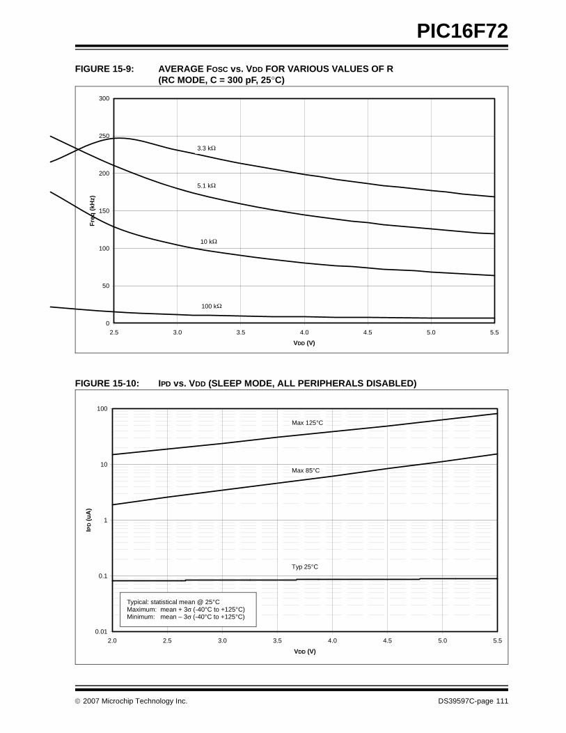
PIC16F72
FIGURE 15-9: AVERAGE FOSC vs. VDD FOR VARIOUS VALUES OF R (RC MODE, C = 300 pF, 25°C)
FIGURE 15-10: IPD vs. VDD (SLEEP MODE, ALL PERIPHERALS DISABLED)
0
50
100
150
200
250
300
2.5 3.0 3.5 4.0 4.5 5.0 5.5
VDD (V)
Fre
q (
kHz)
3.3 kΩ
5.1 kΩ
10 kΩ
100 kΩ
0.01
0.1
1
10
100
2.0 2.5 3.0 3.5 4.0 4.5 5.0 5.5
VDD (V)
IPD
(u
A)
Max 125°C
Max 85°C
Typ 25°C
Typical: statistical mean @ 25°CMaximum: mean + 3σ (-40°C to +125°C) Minimum: mean – 3σ (-40°C to +125°C)
© 2007 Microchip Technology Inc. DS39597C-page 111
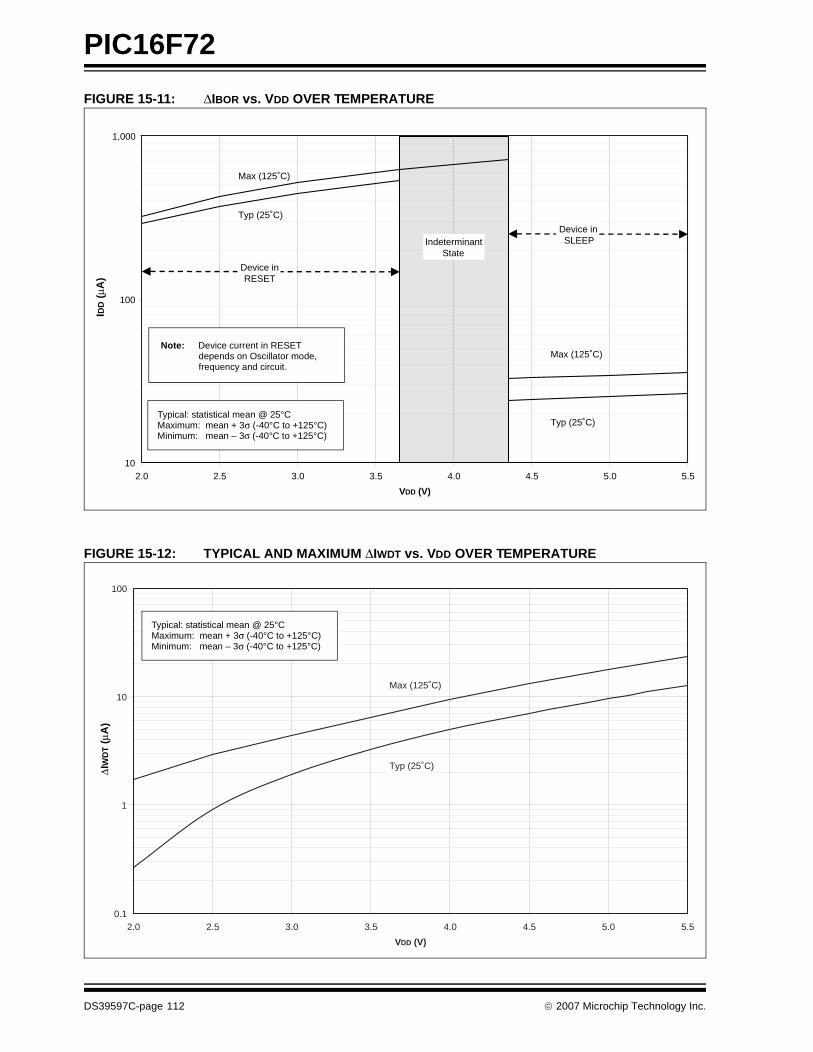
PIC16F72
FIGURE 15-11: ΔIBOR vs. VDD OVER TEMPERATURE
FIGURE 15-12: TYPICAL AND MAXIMUM ΔIWDT vs. VDD OVER TEMPERATURE
10
100
1,000
2.0 2.5 3.0 3.5 4.0 4.5 5.0 5.5
VDD (V)
Device inRESET
Device inSLEEPIndeterminant
State
Max (125˚C)
Typ (25˚C)
Max (125˚C)
Typ (25˚C)Typical: statistical mean @ 25°CMaximum: mean + 3σ (-40°C to +125°C) Minimum: mean – 3σ (-40°C to +125°C)
Note: Device current in RESET depends on Oscillator mode, frequency and circuit.
IDD
(μA
)
0.1
1
10
100
2.0 2.5 3.0 3.5 4.0 4.5 5.0 5.5
VDD (V)
Max (125˚C)
Typ (25˚C)
Typical: statistical mean @ 25°CMaximum: mean + 3σ (-40°C to +125°C) Minimum: mean – 3σ (-40°C to +125°C)
ΔIW
DT (
μA)
DS39597C-page 112 © 2007 Microchip Technology Inc.

PIC16F72
FIGURE 15-13: TYPICAL, MINIMUM AND MAXIMUM WDT PERIOD vs. VDD (-40°C TO +125°C)
FIGURE 15-14: AVERAGE WDT PERIOD vs. VDD OVER TEMPERATURE (-40°C TO +125°C)
0
5
10
15
20
25
30
35
40
45
50
2.0 2.5 3.0 3.5 4.0 4.5 5.0 5.5
VDD (V)
WD
T P
erio
d (
ms)
Max(125°C)
Typ(25°C)
Min(-40°C)
16F77
Typical: statistical mean @ 25°CMaximum: mean + 3σ (-40°C to +125°C) Minimum: mean – 3σ (-40°C to +125°C)
0
5
10
15
20
25
30
35
40
45
50
2.0 2.5 3.0 3.5 4.0 4.5 5.0 5.5
VDD (V)
WD
T P
erio
d (
ms)
125°C
85°C
25°C
-40°C
Typical: statistical mean @ 25°CMaximum: mean + 3σ (-40°C to +125°C) Minimum: mean – 3σ (-40°C to +125°C)
© 2007 Microchip Technology Inc. DS39597C-page 113

PIC16F72
FIGURE 15-15: TYPICAL, MINIMUM AND MAXIMUM VOH vs. IOH (VDD = 5V, -40°C TO +125°C)
FIGURE 15-16: TYPICAL, MINIMUM AND MAXIMUM VOH vs. IOH (VDD = 3V, -40°C TO +125°C)
0.0
0.5
1.0
1.5
2.0
2.5
3.0
3.5
4.0
4.5
5.0
5.5
0 5 10 15 20 25
IOH (-mA)
VO
H (
V)
Max
Typ (25°C)
Min
Typical: statistical mean @ 25°CMaximum: mean + 3σ (-40°C to +125°C) Minimum: mean – 3σ (-40°C to +125°C)
0.0
0.5
1.0
1.5
2.0
2.5
3.0
3.5
0 5 10 15 20 25
IOH (-mA)
VO
H (
V)
Max
Typ (25°C)
Min
Typical: statistical mean @ 25°CMaximum: mean + 3σ (-40°C to +125°C) Minimum: mean – 3σ (-40°C to +125°C)
DS39597C-page 114 © 2007 Microchip Technology Inc.
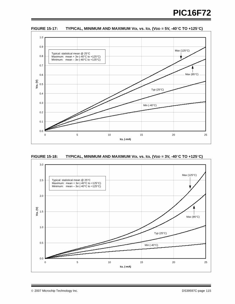
PIC16F72
FIGURE 15-17: TYPICAL, MINIMUM AND MAXIMUM VOL vs. IOL (VDD = 5V, -40°C TO +125°C)
FIGURE 15-18: TYPICAL, MINIMUM AND MAXIMUM VOL vs. IOL (VDD = 3V, -40°C TO +125°C)
0.0
0.1
0.2
0.3
0.4
0.5
0.6
0.7
0.8
0.9
1.0
0 5 10 15 20 25
IOL (-mA)
VO
L (
V)
Max (125°C)
Max (85°C)
Typ (25°C)
Min (-40°C)
Typical: statistical mean @ 25°CMaximum: mean + 3σ (-40°C to +125°C) Minimum: mean – 3σ (-40°C to +125°C)
0.0
0.5
1.0
1.5
2.0
2.5
3.0
0 5 10 15 20 25
IOL (-mA)
VO
L (
V)
Max (125°C)
Max (85°C)
Typ (25°C)
Min (-40°C)
Typical: statistical mean @ 25°CMaximum: mean + 3σ (-40°C to +125°C) Minimum: mean – 3σ (-40°C to +125°C)
© 2007 Microchip Technology Inc. DS39597C-page 115
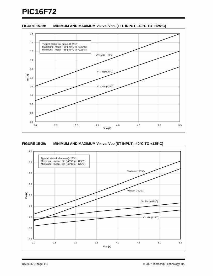
PIC16F72
FIGURE 15-19: MINIMUM AND MAXIMUM VIN vs. VDD, (TTL INPUT, -40°C TO +125°C)
FIGURE 15-20: MINIMUM AND MAXIMUM VIN vs. VDD (ST INPUT, -40°C TO +125°C)
0.5
0.6
0.7
0.8
0.9
1.0
1.1
1.2
1.3
1.4
1.5
2.0 2.5 3.0 3.5 4.0 4.5 5.0 5.5VDD (V)
VIN
(V
)
VTH Max (-40°C)
VTH Min (125°C)
VTH Typ (25°C)
Typical: statistical mean @ 25°CMaximum: mean + 3σ (-40°C to +125°C) Minimum: mean – 3σ (-40°C to +125°C)
0.0
0.5
1.0
1.5
2.0
2.5
3.0
3.5
4.0
2.0 2.5 3.0 3.5 4.0 4.5 5.0 5.5
VDD (V)
VIN
(V
)
VIH Max (125°C)
VIH Min (-40°C)
VIL Max (-40°C)
VIL Min (125°C)
Typical: statistical mean @ 25°CMaximum: mean + 3σ (-40°C to +125°C) Minimum: mean – 3σ (-40°C to +125°C)
DS39597C-page 116 © 2007 Microchip Technology Inc.
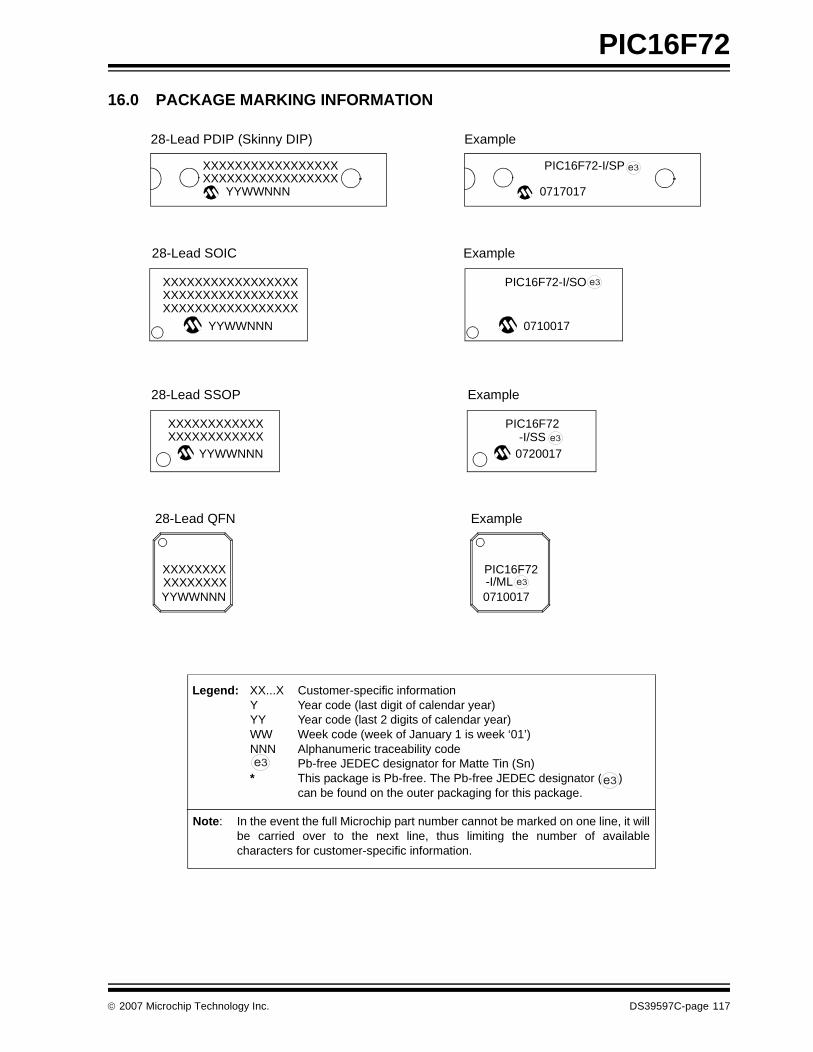
PIC16F72
16.0 PACKAGE MARKING INFORMATION
Legend: XX...X Customer-specific informationY Year code (last digit of calendar year)YY Year code (last 2 digits of calendar year)WW Week code (week of January 1 is week ‘01’)NNN Alphanumeric traceability code Pb-free JEDEC designator for Matte Tin (Sn)* This package is Pb-free. The Pb-free JEDEC designator ( )
can be found on the outer packaging for this package.
Note: In the event the full Microchip part number cannot be marked on one line, it willbe carried over to the next line, thus limiting the number of availablecharacters for customer-specific information.
3e
3e
28-Lead SOIC
YYWWNNN
Example
XXXXXXXXXXXXXXXXXYYWWNNN
28-Lead PDIP (Skinny DIP) Example
XXXXXXXXXXXXXXXXXXXXXXXXXXXXXXXXXX
XXXXXXXXXXXXXXXXX
XXXXXXXXXXXXXXXXX
0717017
PIC16F72-I/SP
0710017
PIC16F72-I/SO
28-Lead SSOP
YYWWNNNXXXXXXXXXXXXXXXXXXXXXXXX
Example
0720017
PIC16F72
28-Lead QFN Example
XXXXXXXXXXXXXXXXYYWWNNN
PIC16F72-I/ML0710017
-I/SS
3e
3e
3e
3e
© 2007 Microchip Technology Inc. DS39597C-page 117

PIC16F72
28-Lead Skinny Plastic Dual In-Line (SP) – 300 mil Body [SPDIP]
Notes:1. Pin 1 visual index feature may vary, but must be located within the hatched area.2. § Significant Characteristic.3. Dimensions D and E1 do not include mold flash or protrusions. Mold flash or protrusions shall not exceed .010" per side.4. Dimensioning and tolerancing per ASME Y14.5M.
BSC: Basic Dimension. Theoretically exact value shown without tolerances.
Note: For the most current package drawings, please see the Microchip Packaging Specification located at http://www.microchip.com/packaging
Units INCHES
Dimension Limits MIN NOM MAX
Number of Pins N 28
Pitch e .100 BSC
Top to Seating Plane A – – .200
Molded Package Thickness A2 .120 .135 .150
Base to Seating Plane A1 .015 – –
Shoulder to Shoulder Width E .290 .310 .335
Molded Package Width E1 .240 .285 .295
Overall Length D 1.345 1.365 1.400
Tip to Seating Plane L .110 .130 .150
Lead Thickness c .008 .010 .015
Upper Lead Width b1 .040 .050 .070
Lower Lead Width b .014 .018 .022
Overall Row Spacing § eB – – .430
NOTE 1
N
1 2
D
E1
eB
c
E
L
A2
eb
b1A1
A
3
Microchip Technology Drawing C04-070B
DS39597C-page 118 © 2007 Microchip Technology Inc.

PIC16F72
28-Lead Plastic Small Outline (SO) – Wide, 7.50 mm Body [SOIC]
Notes:1. Pin 1 visual index feature may vary, but must be located within the hatched area.2. § Significant Characteristic.3. Dimensions D and E1 do not include mold flash or protrusions. Mold flash or protrusions shall not exceed 0.15 mm per side.4. Dimensioning and tolerancing per ASME Y14.5M.
BSC: Basic Dimension. Theoretically exact value shown without tolerances.REF: Reference Dimension, usually without tolerance, for information purposes only.
Note: For the most current package drawings, please see the Microchip Packaging Specification located at http://www.microchip.com/packaging
Units MILLMETERS
Dimension Limits MIN NOM MAX
Number of Pins N 28
Pitch e 1.27 BSC
Overall Height A – – 2.65
Molded Package Thickness A2 2.05 – –
Standoff § A1 0.10 – 0.30
Overall Width E 10.30 BSC
Molded Package Width E1 7.50 BSC
Overall Length D 17.90 BSC
Chamfer (optional) h 0.25 – 0.75
Foot Length L 0.40 – 1.27
Footprint L1 1.40 REF
Foot Angle Top φ 0° – 8°
Lead Thickness c 0.18 – 0.33
Lead Width b 0.31 – 0.51
Mold Draft Angle Top α 5° – 15°
Mold Draft Angle Bottom β 5° – 15°
c
h
h
L
L1
A2
A1
A
NOTE 1
1 2 3
b
e
E
E1
D
φ
β
α
N
Microchip Technology Drawing C04-052B
© 2007 Microchip Technology Inc. DS39597C-page 119
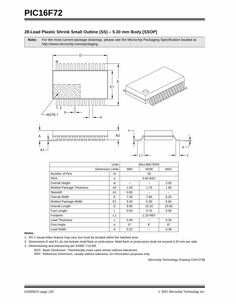
PIC16F72
28-Lead Plastic Shrink Small Outline (SS) – 5.30 mm Body [SSOP]
Notes:1. Pin 1 visual index feature may vary, but must be located within the hatched area.2. Dimensions D and E1 do not include mold flash or protrusions. Mold flash or protrusions shall not exceed 0.20 mm per side.3. Dimensioning and tolerancing per ASME Y14.5M.
BSC: Basic Dimension. Theoretically exact value shown without tolerances.REF: Reference Dimension, usually without tolerance, for information purposes only.
Note: For the most current package drawings, please see the Microchip Packaging Specification located at http://www.microchip.com/packaging
Units MILLIMETERS
Dimension Limits MIN NOM MAX
Number of Pins N 28
Pitch e 0.65 BSC
Overall Height A – – 2.00
Molded Package Thickness A2 1.65 1.75 1.85
Standoff A1 0.05 – –
Overall Width E 7.40 7.80 8.20
Molded Package Width E1 5.00 5.30 5.60
Overall Length D 9.90 10.20 10.50
Foot Length L 0.55 0.75 0.95
Footprint L1 1.25 REF
Lead Thickness c 0.09 – 0.25
Foot Angle φ 0° 4° 8°
Lead Width b 0.22 – 0.38
LL1
c
A2
A1
A
E
E1
D
N
1 2
NOTE 1b
e
φ
Microchip Technology Drawing C04-073B
DS39597C-page 120 © 2007 Microchip Technology Inc.
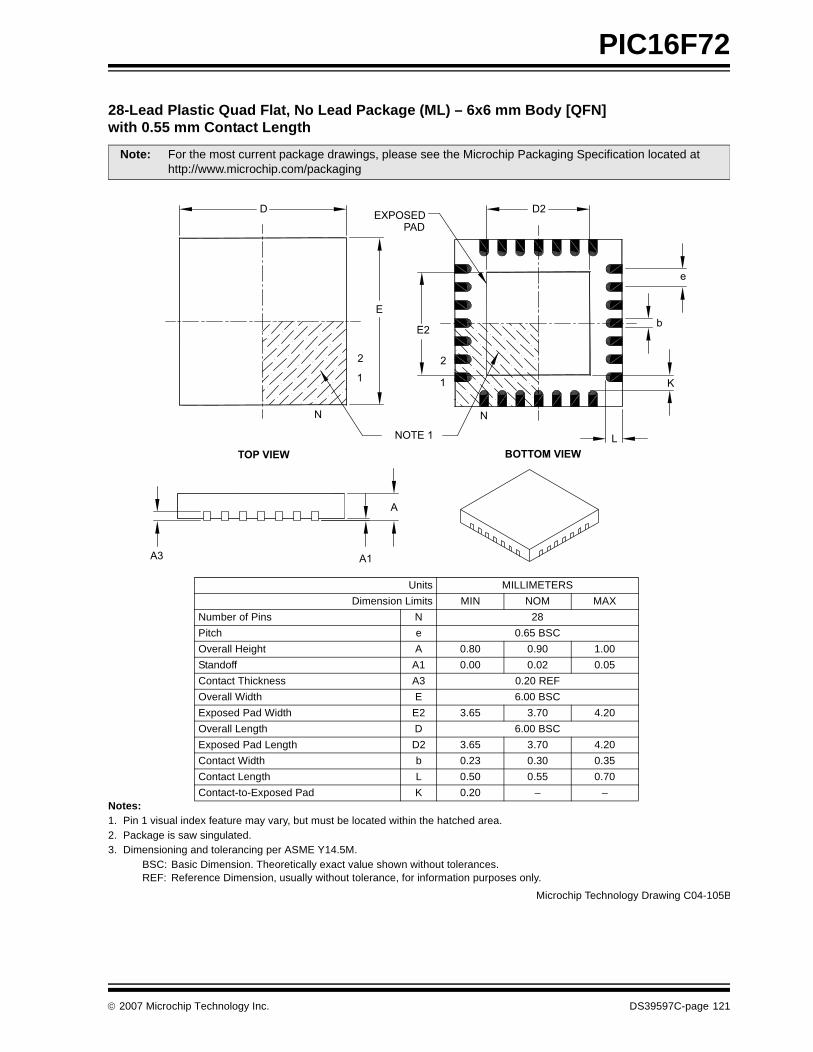
PIC16F72
28-Lead Plastic Quad Flat, No Lead Package (ML) – 6x6 mm Body [QFN]with 0.55 mm Contact Length
Notes:1. Pin 1 visual index feature may vary, but must be located within the hatched area.2. Package is saw singulated.3. Dimensioning and tolerancing per ASME Y14.5M.
BSC: Basic Dimension. Theoretically exact value shown without tolerances.REF: Reference Dimension, usually without tolerance, for information purposes only.
Note: For the most current package drawings, please see the Microchip Packaging Specification located at http://www.microchip.com/packaging
Units MILLIMETERS
Dimension Limits MIN NOM MAX
Number of Pins N 28
Pitch e 0.65 BSC
Overall Height A 0.80 0.90 1.00
Standoff A1 0.00 0.02 0.05
Contact Thickness A3 0.20 REF
Overall Width E 6.00 BSC
Exposed Pad Width E2 3.65 3.70 4.20
Overall Length D 6.00 BSC
Exposed Pad Length D2 3.65 3.70 4.20
Contact Width b 0.23 0.30 0.35
Contact Length L 0.50 0.55 0.70
Contact-to-Exposed Pad K 0.20 – –
DEXPOSED
D2
e
b
K
E2
E
L
N
NOTE 1
1
22
1
N
A
A1A3
TOP VIEW BOTTOM VIEW
PAD
Microchip Technology Drawing C04-105B
© 2007 Microchip Technology Inc. DS39597C-page 121

PIC16F72
NOTES:
DS39597C-page 122 © 2007 Microchip Technology Inc.
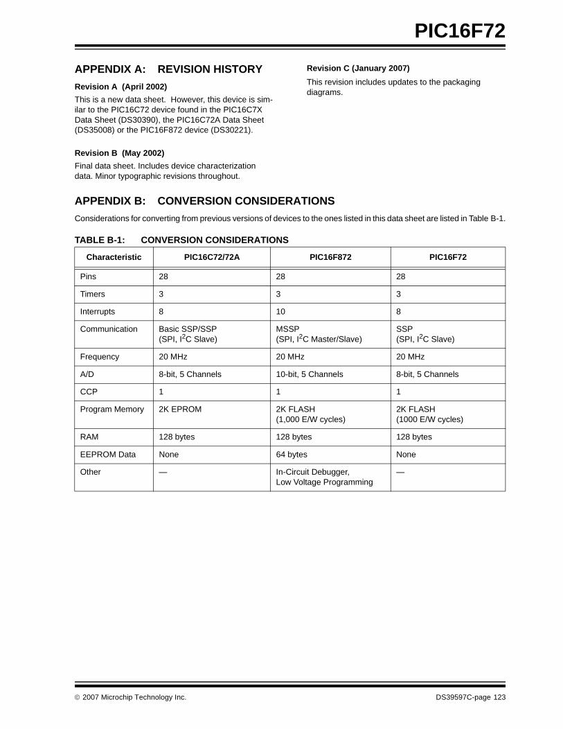
PIC16F72
APPENDIX A: REVISION HISTORY
Revision A (April 2002)
This is a new data sheet. However, this device is sim-ilar to the PIC16C72 device found in the PIC16C7X Data Sheet (DS30390), the PIC16C72A Data Sheet (DS35008) or the PIC16F872 device (DS30221).
Revision B (May 2002)
Final data sheet. Includes device characterization data. Minor typographic revisions throughout.
Revision C (January 2007)
This revision includes updates to the packaging diagrams.
APPENDIX B: CONVERSION CONSIDERATIONS
Considerations for converting from previous versions of devices to the ones listed in this data sheet are listed in Table B-1.
TABLE B-1: CONVERSION CONSIDERATIONS
Characteristic PIC16C72/72A PIC16F872 PIC16F72
Pins 28 28 28
Timers 3 3 3
Interrupts 8 10 8
Communication Basic SSP/SSP(SPI, I2C Slave)
MSSP (SPI, I2C Master/Slave)
SSP (SPI, I2C Slave)
Frequency 20 MHz 20 MHz 20 MHz
A/D 8-bit, 5 Channels 10-bit, 5 Channels 8-bit, 5 Channels
CCP 1 1 1
Program Memory 2K EPROM 2K FLASH (1,000 E/W cycles)
2K FLASH (1000 E/W cycles)
RAM 128 bytes 128 bytes 128 bytes
EEPROM Data None 64 bytes None
Other — In-Circuit Debugger, Low Voltage Programming
—
© 2007 Microchip Technology Inc. DS39597C-page 123
PIC16F72
NOTES:
DS39597C-page 124 © 2007 Microchip Technology Inc.
PIC16F72
INDEX
AA/D
Acquisition Requirements ........................................... 56ADCON0 Register....................................................... 53ADCON1 Register....................................................... 53ADIF bit ....................................................................... 54ADRES Register ......................................................... 53Analog-to-Digital Converter......................................... 53Associated Registers .................................................. 57Configuring Analog Port Pins...................................... 56Configuring the Interrupt ............................................. 54Configuring the Module............................................... 54Conversion Clock........................................................ 56Conversions ................................................................ 56Converter Characteristics ......................................... 104Effects of a RESET ..................................................... 57Internal Sampling Switch (Rss) Impedance ................ 56Operation During SLEEP............................................ 57Source Impedance...................................................... 56Use of the the CCP Trigger......................................... 57
Absolute Maximum Ratings ................................................ 87ACK..................................................................................... 49ADCON0
GO/DONE bit ...................................................... 54ADRES Register ............................................................. 9, 54Application Notes
AN546 (Using the Analog-to-Digital Converter) .......... 53AN552 (Implementing Wake-up on
Key Strokes Using PIC16F7X)............................... 23AN556 (Implementing a Table Read).......................... 19AN578 (Use of the SSP Module in the
I2C Multi-Master Environment)............................... 43AN607 (Power-up Trouble Shooting) .......................... 64
AssemblerMPASM Assembler ..................................................... 81
BBF ....................................................................................... 44Block Diagrams
A/D .............................................................................. 55Analog Input Model ..................................................... 55Capture Mode Operation ............................................ 38Compare Mode Operation .......................................... 39In-Circuit Serial Programming Connections................ 72Interrupt Logic ............................................................. 68On-Chip Reset Circuit ................................................. 63PIC16F72...................................................................... 5PORTC ....................................................................... 25PWM ........................................................................... 41RA3:RA0 and RA5 Port Pins ...................................... 21RA4/T0CKI Pin............................................................ 21RB3:RB0 Port Pins ..................................................... 23RB7:RB4 Port Pins ..................................................... 23Recommended MCLR Circuit ..................................... 63SSP in I2C Mode......................................................... 48SSP in SPI Mode ........................................................ 46Timer0/WDT Prescaler................................................ 29Timer1......................................................................... 32Timer2......................................................................... 35Watchdog Timer (WDT) .............................................. 70
BOR. See Brown-out ResetBrown-out Reset (BOR) .................................... 59, 62, 65, 66Buffer Full Status bit, BF ..................................................... 44
CCapture/Compare/PWM ..................................................... 37
Associated Registers with PWM and Timer2.............. 42Associated Registers, Capture, Compare
and Timer1............................................................. 40Capture
CCP1IF............................................................... 38CCPR1 ............................................................... 38CCPR1H:CCPR1L.............................................. 38
Capture Mode............................................................. 38CCP Mode Timer Resources...................................... 37CCP Pin Configuration ......................................... 38, 39CCP Prescaler............................................................ 38CCPR1L Register ....................................................... 37Compare Mode........................................................... 39PWM Mode................................................................. 41PWM, Example Frequencies/Resolutions .................. 42Software Interrupt ....................................................... 38Software Interrupt Mode ............................................. 39Special Event Trigger and A/D Conversions .............. 39Special Event Trigger Output of CCP1 ....................... 39Timer1 Mode Selection......................................... 38, 39
CCPR1H Register............................................................... 37CCPxM0 bit......................................................................... 37CCPxM1 bit......................................................................... 37CCPxM2 bit......................................................................... 37CCPxM3 bit......................................................................... 37CCPxX bit ........................................................................... 37CCPxY bit ........................................................................... 37CKE .................................................................................... 44CKP .................................................................................... 45Clock Polarity Select bit, CKP............................................. 45Code Examples
Changing Between Capture Prescalers ..................... 38FLASH Program Read................................................ 28Indirect Addressing..................................................... 19Initializing PORTA....................................................... 21Initializing PORTB ...................................................... 23Initializing PORTC ...................................................... 25Saving STATUS, W and PCLATH
Registers in RAM................................................... 69Code Protection............................................................ 59, 72Configuration Bits ............................................................... 59Configuration Word............................................................. 60Conversion Considerations............................................... 123
DD/A...................................................................................... 44Data Memory
General Purpose Register File ..................................... 7Special Function Registers........................................... 9
Data/Address bit, D/A ......................................................... 44DC and AC Characteristics
Graphs and Tables ................................................... 107DC Characteristics.............................................................. 89Development Support ......................................................... 81Device Overview................................................................... 5Direct Addressing ............................................................... 20
EElectrical Characteristics .................................................... 87Errata .................................................................................... 3
© 2007 Microchip Technology Inc. DS39597C-page 125
PIC16F72
FFLASH Program Memory
Associated Registers .................................................. 28Operation During Code Protect................................... 28Reading....................................................................... 28
FSR Register................................................................... 9, 10
II/O Ports .............................................................................. 21
PORTA ........................................................................ 21PORTB........................................................................ 23PORTC........................................................................ 25
I2CAssociated Registers .................................................. 51Master Mode ............................................................... 51Mode Selection ........................................................... 48Multi-Master Mode ...................................................... 51SCL and SDA pins ...................................................... 48Slave Mode ................................................................. 48
ICEPIC In-Circuit Emulator ................................................. 82ID Locations ........................................................................ 72In-Circuit Serial Programming (ICSP) ................................. 72INDF Register ..................................................................... 10Indirect Addressing ............................................................. 20
FSR Register .............................................................. 19INDF Register ............................................................. 19
Instruction Format ............................................................... 73Instruction Set ..................................................................... 73
ADDLW ....................................................................... 75ADDWF....................................................................... 75ANDLW ....................................................................... 75ANDWF....................................................................... 75BCF............................................................................. 75BSF ............................................................................. 75BTFSC ........................................................................ 76BTFSS ........................................................................ 76CALL ........................................................................... 76CLRF........................................................................... 76CLRW.......................................................................... 76CLRWDT..................................................................... 76COMF ......................................................................... 77DECF .......................................................................... 77DECFSZ...................................................................... 77GOTO.......................................................................... 77INCF............................................................................ 77INCFSZ ....................................................................... 77IORLW......................................................................... 78IORWF ........................................................................ 78MOVF.......................................................................... 78MOVLW....................................................................... 78MOVWF ...................................................................... 78NOP ............................................................................ 78RETFIE ....................................................................... 79RETLW........................................................................ 79RETURN ..................................................................... 79RLF ............................................................................. 79RRF............................................................................. 79SLEEP ........................................................................ 79SUBLW........................................................................ 80SUBWF ....................................................................... 80Summary Table ........................................................... 74SWAPF ....................................................................... 80XORLW ....................................................................... 80XORWF....................................................................... 80
INT Interrupt (RB0/INT). See Interrupt SourcesINTCON Register
GIE bit......................................................................... 14INTE bit....................................................................... 14INTF bit ....................................................................... 14RBIF bit....................................................................... 14TMR0IE bit.................................................................. 14
Internal Sampling Switch (Rss) Impedance........................ 56Interrupt Sources .......................................................... 59, 68
RB0/INT Pin, External................................................. 69TMR0 Overflow........................................................... 69
InterruptsRB7:RB4 Port Change................................................ 23Synchronous Serial Port Interrupt............................... 16
Interrupts, Context Saving During....................................... 69Interrupts, Enable Bits
Global Interrupt Enable (GIE bit) .......................... 14, 68Interrupt-on-Change (RB7:RB4)
Enable (RBIE bit) ................................................... 69RB0/INT Enable (INTE bit) ......................................... 14TMR0 Overflow Enable (TMR0IE bit) ......................... 14
Interrupts, Flag bitsInterrupt-on-Change (RB7:RB4) Flag
(RBIF bit) ............................................................... 14Interrupt-on-Change (RB7:RB4) Flag
(RBIF bit) ......................................................... 14, 69RB0/INT Flag (INTF bit).............................................. 14TMR0 Overflow Flag (TMR0IF bit).............................. 69
KKEELOQ Evaluation and Programming Tools ...................... 84
LLoading of PC ..................................................................... 18
MMaster Clear (MCLR)
MCLR Reset, Normal Operation..................... 62, 65, 66MCLR Reset, SLEEP...................................... 62, 65, 66Operation and ESD Protection ................................... 63
MemoryData Memory ................................................................ 7Program Memory .......................................................... 7
MPLAB C17 and MPLAB C18 C Compilers ....................... 81MPLAB ICD In-Circuit Debugger ........................................ 83MPLAB ICE High Performance Universal
In-Circuit Emulator with MPLAB IDE ............................ 82MPLAB Integrated Development
Environment Software .................................................. 81MPLINK Object Linker/MPLIB Object Librarian .................. 82
OOn-Line Support ............................................................... 131OPCODE Field Descriptions............................................... 73OPTION_REG Register
INTEDG bit ................................................................. 13PS2:PS0 bits............................................................... 13PSA bit........................................................................ 13RBPU bit ..................................................................... 13T0CS bit...................................................................... 13T0SE bit ...................................................................... 13
DS39597C-page 126 © 2007 Microchip Technology Inc.

PIC16F72
Oscillator Configuration................................................. 59, 61Crystal Oscillator/Ceramic Resonators ....................... 61HS......................................................................... 61, 65LP.......................................................................... 61, 65RC................................................................... 61, 62, 65XT ......................................................................... 61, 65
Oscillator, WDT................................................................... 70
PP.......................................................................................... 44Package Marking Information ........................................... 117PCFG0 bit ........................................................................... 54PCFG1 bit ........................................................................... 54PCFG2 bit ........................................................................... 54PCL Register............................................................. 9, 10, 18PCLATH Register ..................................................... 9, 10, 18PCON Register ................................................................... 64
POR bit ....................................................................... 17PICDEM 1 Low Cost PIC
Demonstration Board.................................................... 83PICDEM 17 Demonstration Board ...................................... 84PICDEM 2 Low Cost PIC16CXX
Demonstration Board.................................................... 83PICDEM 3 Low Cost PIC16CXXX
Demonstration Board.................................................... 84PICSTART Plus Entry Level
Development Programmer ........................................... 83Pin Functions
MCLR/VPP..................................................................... 6OSC1/CLKI ................................................................... 6OSC2/CLKO ................................................................. 6RA0/AN0 ....................................................................... 6RA1/AN1 ....................................................................... 6RA2/AN2 ....................................................................... 6RA3/AN3/VREF .............................................................. 6RA4/T0CKI.................................................................... 6RA5/AN4/SS ................................................................. 6RB0/INT ........................................................................ 6RB1 ............................................................................... 6RB2 ............................................................................... 6RB3 ............................................................................... 6RB4 ............................................................................... 6RB5 ............................................................................... 6RB6/PGC ...................................................................... 6RB7/PGD ...................................................................... 6RC0/T1OSO/T1CKI ...................................................... 6RC1/T1OSI ................................................................... 6RC2/CCP1 .................................................................... 6RC3/SCK/SCL .............................................................. 6RC4/SDI/SDA ............................................................... 6RC5/SDO ...................................................................... 6RC6............................................................................... 6RC7............................................................................... 6VDD ............................................................................... 6VSS................................................................................ 6
Pinout DescriptionsPIC16F72...................................................................... 6
POP .................................................................................... 19POR. See Power-on ResetPORTA
Associated Registers .................................................. 22Functions .................................................................... 22
PORTA Register ................................................................... 9PORTB
Associated Registers.................................................. 24Functions .................................................................... 24Pull-up Enable (RBPU bit) .......................................... 13RB0/INT Edge Select (INTEDG bit)............................ 13RB0/INT Pin, External ................................................ 69RB7:RB4 Interrupt-on-Change Flag (RBIF bit) ........... 14RB7:RB4 Interrupt-on-Change ................................... 69RB7:RB4 Interrupt-on-Change Enable
(RBIE bit) ............................................................... 69RB7:RB4 Interrupt-on-Change Flag
(RBIF bit) ......................................................... 14, 69PORTB Register ................................................................... 9PORTC
Associated Registers.................................................. 26Functions .................................................................... 26
PORTC Register................................................................... 9Postscaler, WDT
Assignment (PSA Bit) ................................................. 13Rate Select (PS2:PS0 bits) ........................................ 13
Power-down Mode. See SLEEPPower-on Reset (POR)............................... 59, 62, 64, 65, 66
Brown-out Reset (BOR).............................................. 64Oscillator Start-up Timer (OST) ............................ 59, 64POR Status (POR bit) ................................................. 17Power Control/Status Register (PCON)...................... 64Power-down (PD bit) .................................................. 62Power-up Timer (PWRT) ...................................... 59, 64Time-out (TO bit) .................................................. 12, 62Time-out Sequence .................................................... 64
PR2 Register ...................................................................... 35Prescaler, Timer0
Assignment (PSA bit) ................................................. 13Rate Select (PS2:PS0 bits) ........................................ 13
PRO MATE II Universal Device Programmer ..................... 83Product Identification System ........................................... 133Program Counter
RESET Conditions...................................................... 65Program Memory
Paging ........................................................................ 19Program Memory Map and Stack ......................................... 7Program Verification ........................................................... 72PUSH.................................................................................. 19
RR/W..................................................................................... 44R/W bit ................................................................................ 49RBIF bit............................................................................... 23Read/Write bit Information, R/W......................................... 44Reader Response............................................................. 132Reading Program Memory.................................................. 27
PMADR....................................................................... 27PMCON1 Register...................................................... 27
Receive Overflow Indicator bit, SSPOV.............................. 45Register File Map.................................................................. 8
© 2007 Microchip Technology Inc. DS39597C-page 127
PIC16F72
Registers ............................................................................. 36ADCON0 (A/D Control 0) ............................................ 53ADCON1 (A/D Control 1) ............................................ 54CCPCON1 (Capture/Compare/PWM Control 1) ......... 37Initialization Conditions (table) .................................... 66INTCON (Interrupt Control) ......................................... 14OPTION ...................................................................... 13PCON (Power Control) ............................................... 17PIE1 (Peripheral Interrupt Enable 1) ........................... 15PIR1 (Peripheral Interrupt Flag 1) ............................... 16PMCON1 (Program Memory Control 1) ...................... 27SSPCON (Sync Serial Port Control) ........................... 45SSPSTAT (Synchronous Serial Port Status) ............... 44STATUS ...................................................................... 12Summary....................................................................... 9T1CON (Timer1 Control) ............................................. 31
RESET .......................................................................... 59, 62Brown-out Reset (BOR). See Brown-out Reset (BOR)MCLR RESET. See MCLRPower-on Reset (POR). See Power-on Reset (POR)RESET Conditions for All Registers............................ 66RESET Conditions for PCON Register ....................... 65RESET Conditions for Program Counter .................... 65RESET Conditions for STATUS Register .................... 65WDT Reset. See Watchdog Timer (WDT)
Revision History ................................................................ 123RP0, RP1 bit ......................................................................... 7
SS.......................................................................................... 44Sales and Support............................................................. 133Slave Mode
SCL ............................................................................. 48SDA............................................................................. 48
SLEEP..................................................................... 59, 62, 71SMP .................................................................................... 44Software Simulator (MPLAB SIM)....................................... 82Special Event Trigger.......................................................... 57Special Features of the CPU............................................... 59Special Function Registers
PMADRH .................................................................... 27PMADRL ..................................................................... 27PMCON1..................................................................... 27PMDATH ..................................................................... 27PMDATL...................................................................... 27
SPIAssociated Registers .................................................. 46
SPI Clock Edge Select bit, CKE.......................................... 44SPI Data Input Sample Phase Select bit, SMP................... 44SPI Mode
Serial Clock................................................................. 43Serial Data In .............................................................. 43Serial Data Out............................................................ 43Slave Select ................................................................ 43
SSPACK............................................................................. 48Addressing .................................................................. 48BF bit........................................................................... 48I2C Mode Operation .................................................... 48R/W bit ........................................................................ 49Reception.................................................................... 49SCL Clock Input .......................................................... 48SSPOV bit ................................................................... 48Transmission............................................................... 49
SSPADD Register............................................................... 10SSPEN................................................................................ 45SSPIF ................................................................................. 16SSPM3:SSPM0 .................................................................. 45SSPOV ............................................................................... 45SSPSTAT Register ............................................................. 10Stack................................................................................... 19
Overflows.................................................................... 19Underflow ................................................................... 19
START bit, S....................................................................... 44STATUS Register
DC bit.......................................................................... 12IRP bit ......................................................................... 12PD bit .......................................................................... 62TO bit .................................................................... 12, 62
STOP bit, P......................................................................... 44Synchronous Serial Port (SSP) .......................................... 43
Overview..................................................................... 43SPI Mode.................................................................... 43
Synchronous Serial Port Enable bit, SSPEN...................... 45Synchronous Serial Port Interrupt....................................... 16Synchronous Serial Port Mode Select bits,
SSPM3:SSPM0............................................................ 45
TT2CKPS0 bit ....................................................................... 36T2CKPS1 bit ....................................................................... 36T2CON (Timer2 Control) .................................................... 36TAD...................................................................................... 56Timer0................................................................................. 29
Clock Source Edge Select (T0SE bit)......................... 13Clock Source Select (T0CS bit) .................................. 13External Clock............................................................. 30Interrupt ...................................................................... 29Operation .................................................................... 29Overflow Enable (TMR0IE bit) .................................... 14Overflow Flag (TMR0IF bit) ........................................ 69Overflow Interrupt ....................................................... 69Prescaler .................................................................... 30T0CKI ......................................................................... 30
Timer1Associated Registers .................................................. 34Asynchronous Counter Mode ..................................... 33Capacitor Selection..................................................... 33Counter Operation ...................................................... 32Interrupt ...................................................................... 33Operation in Timer Mode ............................................ 32Oscillator..................................................................... 33Prescaler .................................................................... 34Resetting TMR1H, TMR1L Register Pair.................... 34Resetting Using a CCP Trigger Output....................... 33Synchronized Counter Mode ...................................... 32
Timer2................................................................................. 35Interrupt ...................................................................... 35Operation .................................................................... 35Output ......................................................................... 35Prescaler, Postscaler .................................................. 35
DS39597C-page 128 © 2007 Microchip Technology Inc.
PIC16F72
Timing DiagramsA/D Conversion......................................................... 105Brown-out Reset ......................................................... 96Capture/Compare/PWM (CCP1)................................. 98CLKO and I/O ............................................................. 95External Clock............................................................. 94I2C Bus Data ............................................................. 102I2C Bus START/STOP bits........................................ 101I2C Reception (7-bit Address) ..................................... 50I2C Transmission (7-bit Address) ................................ 50RESET, Watchdog Timer, Oscillator Start-up Timer
and Power-up Timer............................................... 96Slow Rise Time (MCLR Tied to VDD Through
RC Network)........................................................... 68SPI Master Mode ........................................................ 47SPI Master Mode (CKE = 0, SMP = 0) ....................... 99SPI Master Mode (CKE = 1, SMP = 1) ....................... 99SPI Slave Mode (CKE = 0) ................................. 47, 100SPI Slave Mode (CKE = 1) ................................. 47, 100Time-out Sequence on Power-up (MCLR Tied to
VDD Through Pull-up Resistor)............................... 67Time-out Sequence on Power-up (MCLR Tied to
VDD Through RC Network): Case 1 ....................... 67Time-out Sequence on Power-up (MCLR Tied to
VDD Through RC Network): Case 2 ....................... 67Timer0 and Timer1 External Clock.............................. 97Wake-up from SLEEP through Interrupt ..................... 72
Timing Parameter Symbology............................................. 93TMR1H Register ................................................................... 9TMR1L Register .................................................................... 9TMR2 Register ...................................................................... 9TMR2ON bit ........................................................................ 36TOUTPS0 bit....................................................................... 36TOUTPS1 bit....................................................................... 36TOUTPS2 bit....................................................................... 36TOUTPS3 bit....................................................................... 36TRISA Register ............................................................. 10, 21TRISB Register ............................................................. 10, 23TRISC Register ............................................................. 10, 25
UUA....................................................................................... 44Update Address bit, UA ...................................................... 44
WWake-up from SLEEP................................................... 59, 71
Interrupts .............................................................. 65, 66MCLR Reset ............................................................... 66WDT Reset ................................................................. 66
Watchdog Timer (WDT)................................................ 59, 70Associated Registers.................................................. 70Enable (WDTEN bit) ................................................... 70Postscaler. See Postscaler, WDTProgramming Considerations ..................................... 70RC Oscillator .............................................................. 70Time-out Period .......................................................... 70WDT Reset, Normal Operation....................... 62, 65, 66WDT Reset, SLEEP ....................................... 62, 65, 66
WCOL................................................................................. 45Write Collision Detect bit, WCOL........................................ 45WWW, On-Line Support ....................................................... 3
© 2007 Microchip Technology Inc. DS39597C-page 129

PIC16F72
NOTES:
DS39597C-page 130 © 2007 Microchip Technology Inc.
DSTEMP
THE MICROCHIP WEB SITE
Microchip provides online support via our WWW site atwww.microchip.com. This web site is used as a meansto make files and information easily available tocustomers. Accessible by using your favorite Internetbrowser, the web site contains the followinginformation:
• Product Support – Data sheets and errata, application notes and sample programs, design resources, user’s guides and hardware support documents, latest software releases and archived software
• General Technical Support – Frequently Asked Questions (FAQ), technical support requests, online discussion groups, Microchip consultant program member listing
• Business of Microchip – Product selector and ordering guides, latest Microchip press releases, listing of seminars and events, listings of Microchip sales offices, distributors and factory representatives
CUSTOMER CHANGE NOTIFICATION SERVICE
Microchip’s customer notification service helps keepcustomers current on Microchip products. Subscriberswill receive e-mail notification whenever there arechanges, updates, revisions or errata related to aspecified product family or development tool of interest.
To register, access the Microchip web site atwww.microchip.com, click on Customer ChangeNotification and follow the registration instructions.
CUSTOMER SUPPORT
Users of Microchip products can receive assistancethrough several channels:
• Distributor or Representative
• Local Sales Office• Field Application Engineer (FAE)• Technical Support
• Development Systems Information Line
Customers should contact their distributor,representative or field application engineer (FAE) forsupport. Local sales offices are also available to helpcustomers. A listing of sales offices and locations isincluded in the back of this document.
Technical support is available through the web siteat: http://support.microchip.com
© 2005 Microchip Technology Inc. Advance Information DS00000A-page 131

DSTEMP
READER RESPONSE
It is our intention to provide you with the best documentation possible to ensure successful use of your Microchip prod-uct. If you wish to provide your comments on organization, clarity, subject matter, and ways in which our documentationcan better serve you, please FAX your comments to the Technical Publications Manager at (480) 792-4150.
Please list the following information, and use this outline to provide us with your comments about this document.
To: Technical Publications Manager
RE: Reader Response
Total Pages Sent ________
From: Name
Company
Address
City / State / ZIP / Country
Telephone: (_______) _________ - _________
Application (optional):
Would you like a reply? Y N
Device: Literature Number:
Questions:
FAX: (______) _________ - _________
DS00000ADSTEMP
1. What are the best features of this document?
2. How does this document meet your hardware and software development needs?
3. Do you find the organization of this document easy to follow? If not, why?
4. What additions to the document do you think would enhance the structure and subject?
5. What deletions from the document could be made without affecting the overall usefulness?
6. Is there any incorrect or misleading information (what and where)?
7. How would you improve this document?
DS00000A-page 132 Advance Information © 2005 Microchip Technology Inc.
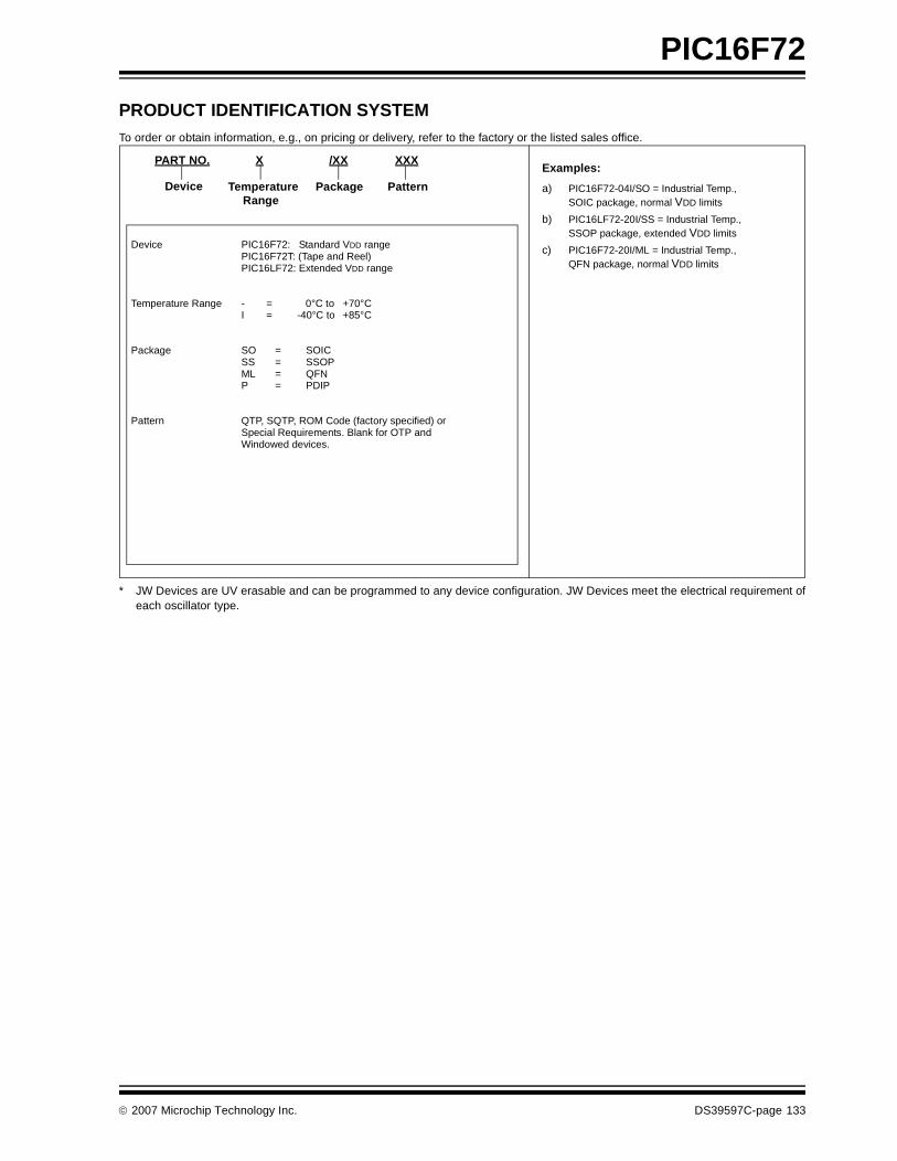
© 2007 Microchip Technology Inc. DS39597C-page 133
PIC16F72
PRODUCT IDENTIFICATION SYSTEMTo order or obtain information, e.g., on pricing or delivery, refer to the factory or the listed sales office.
* JW Devices are UV erasable and can be programmed to any device configuration. JW Devices meet the electrical requirement ofeach oscillator type.
PART NO. X /XX XXX
PatternPackageTemperatureRange
Device
Device PIC16F72: Standard VDD rangePIC16F72T: (Tape and Reel)PIC16LF72: Extended VDD range
Temperature Range - = 0°C to +70°CI = -40°C to +85°C
Package SO = SOICSS = SSOPML = QFNP = PDIP
Pattern QTP, SQTP, ROM Code (factory specified) or Special Requirements. Blank for OTP and Windowed devices.
Examples:
a) PIC16F72-04I/SO = Industrial Temp.,SOIC package, normal VDD limits
b) PIC16LF72-20I/SS = Industrial Temp.,SSOP package, extended VDD limits
c) PIC16F72-20I/ML = Industrial Temp.,QFN package, normal VDD limits
DS39597C-page 134 © 2007 Microchip Technology Inc.
AMERICASCorporate Office2355 West Chandler Blvd.Chandler, AZ 85224-6199Tel: 480-792-7200 Fax: 480-792-7277Technical Support: http://support.microchip.comWeb Address: www.microchip.com
AtlantaDuluth, GA Tel: 678-957-9614 Fax: 678-957-1455
BostonWestborough, MA Tel: 774-760-0087 Fax: 774-760-0088
ChicagoItasca, IL Tel: 630-285-0071 Fax: 630-285-0075
DallasAddison, TX Tel: 972-818-7423 Fax: 972-818-2924
DetroitFarmington Hills, MI Tel: 248-538-2250Fax: 248-538-2260
KokomoKokomo, IN Tel: 765-864-8360Fax: 765-864-8387
Los AngelesMission Viejo, CA Tel: 949-462-9523 Fax: 949-462-9608
Santa ClaraSanta Clara, CA Tel: 408-961-6444Fax: 408-961-6445
TorontoMississauga, Ontario, CanadaTel: 905-673-0699 Fax: 905-673-6509
ASIA/PACIFICAsia Pacific OfficeSuites 3707-14, 37th FloorTower 6, The GatewayHabour City, KowloonHong KongTel: 852-2401-1200Fax: 852-2401-3431
Australia - SydneyTel: 61-2-9868-6733Fax: 61-2-9868-6755
China - BeijingTel: 86-10-8528-2100 Fax: 86-10-8528-2104
China - ChengduTel: 86-28-8665-5511Fax: 86-28-8665-7889
China - FuzhouTel: 86-591-8750-3506 Fax: 86-591-8750-3521
China - Hong Kong SARTel: 852-2401-1200 Fax: 852-2401-3431
China - QingdaoTel: 86-532-8502-7355Fax: 86-532-8502-7205
China - ShanghaiTel: 86-21-5407-5533 Fax: 86-21-5407-5066
China - ShenyangTel: 86-24-2334-2829Fax: 86-24-2334-2393
China - ShenzhenTel: 86-755-8203-2660 Fax: 86-755-8203-1760
China - ShundeTel: 86-757-2839-5507 Fax: 86-757-2839-5571
China - WuhanTel: 86-27-5980-5300Fax: 86-27-5980-5118
China - XianTel: 86-29-8833-7250Fax: 86-29-8833-7256
ASIA/PACIFICIndia - BangaloreTel: 91-80-4182-8400 Fax: 91-80-4182-8422
India - New DelhiTel: 91-11-4160-8631Fax: 91-11-4160-8632
India - PuneTel: 91-20-2566-1512Fax: 91-20-2566-1513
Japan - YokohamaTel: 81-45-471- 6166 Fax: 81-45-471-6122
Korea - GumiTel: 82-54-473-4301Fax: 82-54-473-4302
Korea - SeoulTel: 82-2-554-7200Fax: 82-2-558-5932 or 82-2-558-5934
Malaysia - PenangTel: 60-4-646-8870Fax: 60-4-646-5086
Philippines - ManilaTel: 63-2-634-9065Fax: 63-2-634-9069
SingaporeTel: 65-6334-8870Fax: 65-6334-8850
Taiwan - Hsin ChuTel: 886-3-572-9526Fax: 886-3-572-6459
Taiwan - KaohsiungTel: 886-7-536-4818Fax: 886-7-536-4803
Taiwan - TaipeiTel: 886-2-2500-6610 Fax: 886-2-2508-0102
Thailand - BangkokTel: 66-2-694-1351Fax: 66-2-694-1350
EUROPEAustria - WelsTel: 43-7242-2244-39Fax: 43-7242-2244-393Denmark - CopenhagenTel: 45-4450-2828 Fax: 45-4485-2829
France - ParisTel: 33-1-69-53-63-20 Fax: 33-1-69-30-90-79
Germany - MunichTel: 49-89-627-144-0 Fax: 49-89-627-144-44
Italy - Milan Tel: 39-0331-742611 Fax: 39-0331-466781
Netherlands - DrunenTel: 31-416-690399 Fax: 31-416-690340
Spain - MadridTel: 34-91-708-08-90Fax: 34-91-708-08-91
UK - WokinghamTel: 44-118-921-5869Fax: 44-118-921-5820
WORLDWIDE SALES AND SERVICE
12/08/06