photovoltaic manufacturing: present status , future ... manufacturing: present status , future...
TRANSCRIPT
1
Photovoltaic Manufacturing: Present Status, Future Prospects and Research Needs
Running title: Photovoltaic Manufacturing
Running Authors: Wolden et al.
Colin A. Woldena),b) Colorado School of Mines, Department of Chemical Engineering, 1500 Illinois Street, Golden CO 80401
Juanita Kurtin Spectrawatt, 7175 Northwest Evergreen Parkway, Hillsboro, OR 97124
Jason B. Baxter a) Drexel University, Department of Chemical and Biological Engineering, 3141 Chestnut St., Philadelphia PA 19104
Ingrid Repins National Renewable Energy Laboratory, Golden CO 80401
Sean E. Shaheen University of Denver, Department of Physics an Astronomy, 2112 East Wesley Avenue, Denver, CO 80208
John T. Torvik Novus Energy Partners, 201 North Union Street, Suite 350, Alexandria, VA 22314
Angus A. Rockett a) University of Illinois, Department of Materials Science and Engineering, 1304 W. Green St. Urbana, IL 61801
Vasilis M. Fthenakis Columbia University and Brookhaven National Laboratory, Upton, NY 11973
Eray S. Aydila) University of Minnesota, Department of Chemical Engineering and Materials Science, 151 Amundson Hall, 421 Washington Avenue SE, Minneapolis, Minnesota 55455
a)American Vacuum Society member. b)Electronic mail: [email protected]
2
Abstract
In May 2010 the United States National Science Foundation sponsored a two-day
workshop to review the state-of-the-art and research challenges in photovoltaic (PV)
manufacturing. This article summarizes the major conclusions and outcomes from this
workshop, which was focused on identifying the science that needs to be done to help
accelerate PV manufacturing. A significant portion of the article focuses on assessing the
current status of and future opportunities in the major PV manufacturing technologies.
These are solar cells based on crystalline silicon (c-Si), thin-films of cadmium telluride
(CdTe), thin-films of copper indium gallium diselenide (CIGS), and thin films of
hydrogenated amorphous and nanocrystalline silicon (a-Si:H or nc-Si:H). Current trends
indicate that c-Si and CdTe performance are evolving beyond the constraints commonly
associated with these technologies. With a focus on TW/year production capacity, the
issue of materials availability is discussed along with the emerging technologies of dye-
sensitized solar cells (DSC) and organic photovoltaics (OPV) that are potentially less
constrained by elemental abundance. Lastly, recommendations are made for research
investment, with an emphasis on those areas that are expected to have cross-cutting
impact.
3
I. INTRODUCTION
Global power consumption currently stands at approximately 15 TW (1 TW =
1012 W), the vast majority of which is generated by the combustion of fossil fuels. The
associated release of CO2 from these anthropogenic sources has dramatically altered the
composition of the atmosphere and may detrimentally impact global temperature, sea
levels, and weather patterns. The terawatt challenge is the effort to supply up to 30 TW of
carbon-free power by the mid 21st century.1 Assuming that all this power will be supplied
by photovoltaics (PV) and the lifetime of solar cells is 30 years, this translates to PV
production of ~ 1 TW/year. While all renewable resources will be important, only solar
can meet this level of demand. The practical global potential of other renewable energy
sources such as wind, hydroelectric, biomass and geothermal is estimated to be less than
10 TW.2 Of the >105 TW of sunlight hitting the earth, it is estimated that harnessing up to
600 TW is technically feasible. Solar energy may be harvested through its conversion to
heat (solar thermal), electrons (PV), or chemicals (solar fuels). The former is perhaps the
most straightforward, with installations ranging in scale from 1 kW household water
heaters to 50 MW power plants located in areas of high solar insolation.3 Common
approaches to solar fuels include the photoelectrochemical splitting of water to produce
H2 and the reduction of CO2 into liquid fuels such as methanol.4 Solar fuels remains the
least developed strategy to harness solar energy, and is currently the focus of renewed
efforts at the basic research level.5
The subject of this article is solar photovoltaics, which has been growing at an
average rate of >40% per year over the past decade, with annual shipments exceeding 8
GW in 2009. That number is projected to double in 2010. Moreover, the market is poised
4
for further expansion in the next decade as PV transitions from a subsidized commodity
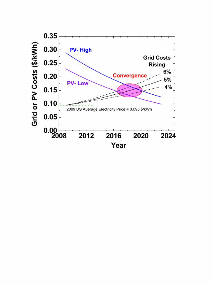
to one that provides outright economic advantage. Figure 1 compares the levelized cost of
solar electricity with that produced by conventional sources. In 2009, the average cost of
grid-supplied electricity in the United States was 9.5 ₵/kWhr, and this value will
continue to rise due to increased demand or at potentially higher rates if measures such as
carbon taxation are introduced. The current price of electricity generated using solar cells
remains 2 to 3 times greater than grid-supplied electricity, but PV costs continue to
decrease. A crossover, commonly called “grid-parity”, is expected sometime during the
next decade. In fact, grid parity has been reached in areas such as Southern California
where solar insolation and the marginal cost of electricity are high. We also note that
projected grid-parity does not require any technological breakthroughs, but is simply an
extrapolation of the learning curve that the PV industry has been following for several
decades, along with the inevitable increase in the cost of fossil fuel derived electricity.6
Despite this amazing success, PV manufacturing must be further expanded by two
orders of magnitude to TW/year production levels in order to transform our society from
one that relies on burning fossil fuels to one that uses sustainable energy sources. The
challenge is daunting, but the opportunities are equally boundless. The sun continuously
provides power to the planet with an average flux of 1000 W/m2. If one assumes 10% net
conversion efficiency (generation, transportation, storage), ~1012 square meters would be
required to supply 30 TW of clean energy. Assuming 30 year panel lifetimes, this
translates into the production of ~5 x 10¹⁰ m2/year. To put this number in perspective, the
global production of all flat glass, which is currently dominated by the construction and
automotive sectors, is about 6 x 10⁹ m2/year. Glass is an appropriate comparison since it
5
is common to the majority of current PV platforms, accounting for a substantial fraction
of the weight and cost of PV panels.
In May 2010, the United States National Science Foundation (NSF) organized a
workshop on the theme of catalyzing innovation in PV manufacturing to help address the
challenges described above. The workshop was co-sponsored by four divisions including
Chemical, Bioengineering, Environmental, and Transport Systems, Industrial Innovation
and Partnerships, Chemistry, and Materials Research. The objectives of the workshop
were as follows.
• Identify the potential technologies and innovations that offer low-cost, high-
conversion-efficiency and sustainable photovoltaics materials.
• Determine the current and potential technical challenges in preparation and/or
manufacture of above photovoltaics materials.
• Facilitate effective and efficient collaborations between small businesses and
universities or large companies in the efforts to overcome these challenges.
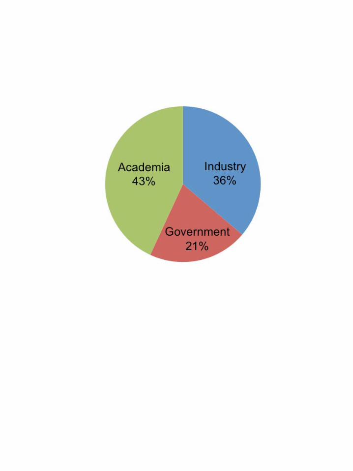
The event was organized and hosted by Colorado School of Mines in Golden,
Colorado. To address this diverse set of goals 60 leaders were invited, with nearly equal
representation between industry and academia (Fig. 2). Scientists from National
laboratories including the National Renewable Energy Laboratory (NREL) and the
National Institute of Standards and Technology (NIST) were also present. A full list of
participants, topics, and presentations from the workshop are available online.7 In this
article, we highlight the major outcomes of the workshop. We begin by briefly
summarizing the current status of PV manufacturing, and then assess the major
6
challenges and opportunities with respect to the major PV manufacturing technologies.
The aggressive goal of TW/year production capacity necessitated the discussion of the
important issue of materials availability for existing technologies. Lastly,
recommendations are made for research investment, with an emphasis on those areas that
are expected to have cross-cutting impact.
II. PRESENT STATUS OF PV MANUFACTURING
This paper is not intended to provide a comprehensive review of the history of
photovoltaics, but rather to update the substantial changes that have occurred since the
turn of the century. This date was chosen for a couple of reasons. First, there are a
number of very good reviews detailing the growth and evolution of the PV industry up to
around 2003.6, 8, 9 Moreover, there have been two significant changes that have
accompanied the growth experienced during the past 7 years. In 2003 various forms of
silicon accounted for >99% of the PV market, and manufacturing was lead by Japan and
Europe.9 Today crystalline silicon (c-Si) still accounts for 85% of the market, but China
has become the world’s leading manufacturer.10 Table I lists the top 10 crystalline Si
manufacturers and their output in 2009.11 In a very short period of time China has moved
from being a negligible player to supplying 50% of the worlds PV modules. This growth
was spurred by strategic government investment, access to cheap capital and has
benefited from low Chinese labor costs that enables module production at lower costs
than its competitors in Japan, Europe, and the US.
The second major change in the past decade has been the emergence of cadmium
telluride (CdTe) thin film technology, which was a negligible contributor in 2003. Figure
3 displays the global market share held by the various PV technologies in 2008 and
7
2009.12 A single company, First Solar, has brought CdTe to mass production. In 2009, it
became the world’s first PV manufacturer to exceed 1 GW/yr production rate and
captured 13% of the global market (Fig. 3). While some of this market share has come at
the expense of c-Si, it has also eroded the foothold of competing thin film technologies
such as amorphous silicon (a-Si:H). However, the distribution of market share continues
to be very fluid, with c-Si expected to regain market share in 2010 due to continued
expansion of PV manufacturing operations in China. The most important point is that the
emergence of CdTe attests to the fast change the PV industry can undergo within a
relatively short period of time. Such shifts are driven by innovations in manufacturing
and fundamental science coupled with creative and aggressive entrepreneurship.
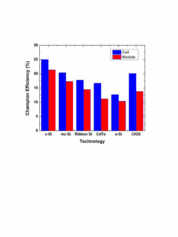
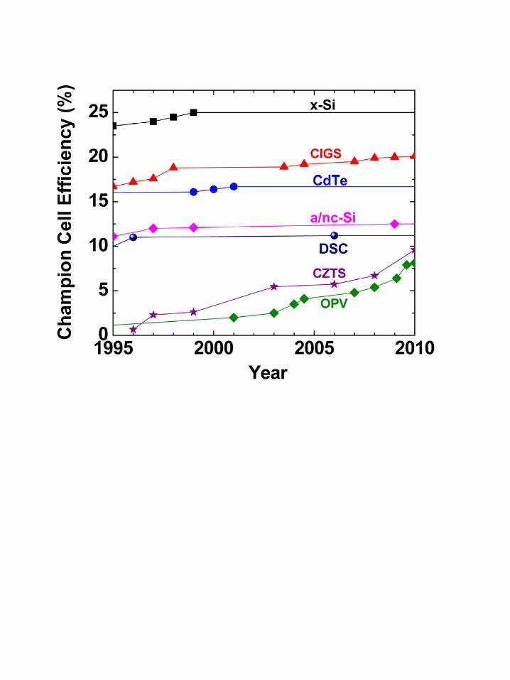
Figure 4 displays the champion overall power conversion efficiencies for
laboratory solar cells and commercial modules for the established PV manufacturing
technologies. Values are from the latest compendium by Green et al.13 with the exception
of ribbon silicon.14, 15 In addition to efficiency, materials and manufacturing costs are the
greatest levers controlling the cost of solar power.16 In most cases, the champion cells
have seen little or no improvement over the past decade while economies of scale and
advances in manufacturing science and technology have fueled the expansion of PV
through cost reduction and module performance improvements. Figure 4 shows that the
PV technologies are at different points in their respective learning curves when compared
to the Shockley–Queisser (S-Q) limit of ~31% solar energy conversion efficiency for
single junction devices.17 Since, the band gap energy dependence of the Shockley–
Queisser limit is flat around the maximum, the theoretical efficiency limits for these
technologies are only marginally different and are not a deciding factor in their
8
competitiveness with each other. Nevertheless, record single crystal (c-Si) cells have
matured to within 90% of their S-Q limit, while commercial thin film modules harvest
about 35% of their potential. The next section reviews the advantages and limitations of
these competing PV technologies.
III. Opportunities and Challenges in Current PV
Manufacturing Technologies
A. Crystalline Silicon
Silicon is the most developed and well-understood semiconductor in the world,
benefiting from decades of development by the integrated circuit (IC) industry.
Techniques to control and manipulate its properties are well established. Silicon has
proven field stability, and it is the most abundant semiconductor in the world. Multi-
crystalline silicon (mc-Si) remains the leading PV product (Fig. 3), though its market
share has ebbed from values as high as 65% earlier in the decade. The combination of
higher efficiency, lower polysilicon prices, and improvements in wire cutting technology
has reduced wafer thicknesses and kept single crystal (c-Si) silicon competitive. The
issues that limit the c-Si technology today remain quite similar to those described by
Goetzberger et al.,8 in their detailed 2003 review article. The cost of the silicon feedstock
remains the biggest lever impacting manufacturing costs. Reducing the cost of silicon is
being pursued through a number of avenues including improving the feedstock,
production of kerfless wafers, and the development of ultrathin silicon, as well as the use
of bifacial cells. These strategies are briefly reviewed below as well as efforts to further
improve module efficiency.
9
1. Silicon feedstock
To date, purification techniques for silicon have been dictated by the IC industry,
which employs electronic grade silicon with purity levels of less than 1 ppb. A significant
shift occurred a few years ago when the PV industry surpassed the IC industry as the
largest consumer of refined silicon. Despite decades of steady growth, this transition
apparently caught silicon suppliers by surprise, leading to short-term shortages and price
spikes in 2008. However silicon foundries have responded to their leading client by both
increasing capacity and examining strategies to develop “solar grade” silicon. Electronic
grade silicon is produced primarily using the energy intensive (>120 kWh/kg) Siemens
process.18 New production strategies such as fluidized bed technology are being
investigated to upgrade metallurgical grade silicon, potentially reducing these energy
requirements by up to a factor of five.19 Though less expensive, these techniques often
retain higher levels of metals such as Fe and Al than electronic grade silicon. While
these impurities would be catastrophic in IC manufacturing, such low levels may be
tolerable in solar cells. An active area of research is focused on establishing the impurity
levels, which can be tolerated by solar cells, as well as devising processing strategies to
mitigate and/or passivate these defects. Such improvements should reduce both the
energy payback time and ecotoxicity associated with silicon production.20
2. Kerfless wafers
Improvements in wire-saw technology have enabled the reduction of wafer
thicknesses to 180 µm at present. However, over 50% of the silicon is lost as silicon
sawdust or Kerf. While this material can be recycled, it would be desirable if the wire-
10
sawing step could be eliminated all together. Kerfless wafer could potentially reduce Si
use from an industry average of about 6 g/W to 3 g/W at current wafer thicknesses.
Techniques for the direct production of wafers from the melt were invented in the
1970s,21, 22 and after decades of development they have now reached the market. The two
closely related techniques are edge-defined, film-fed growth (EFG) and string ribbon
silicon technologies. In the EFG process the Si wafers are pulled out from the melt
through a graphite die using capillary action. This process was developed extensively by
ASE Americas23 and is now employed by Schott Solar. Ribbon silicon is produced by
pulling a pair of high-temperature strings through a crucible of molten Si, and this
technology has been promoted and implemented by Evergreen Solar. These two growth
techniques produce vertical sheets of mc-Si approximately 300 µm thick and up to a 100
mm wide. The elimination of wafer sawing makes this the most energy efficient mode to
produce c-Si, and companies using these methods claim that energy payback times have
been reduced to one year. The quality of the material produced by these techniques is
somewhat inferior to standard block-cast mc-Si, but is continuously improving with
champion laboratory cells now reaching power conversion efficiencies over 18% and
14.5% efficient modules already on the market.14, 15 Passivation of surface and bulk
defects is critical to achieving high efficiency, and this is usually achieved through the
deposition of a hydrogen-rich silicon nitride layer, which also serves as an anti-reflection
(AR) coating.24 These technologies are expected to become more cost-competitive as
energy costs continue to rise, but improvements in manufacturing are needed to compete
with conventional c-Si technology (Fig. 3). In particular, further reductions in wafer
thickness coupled to improvements in throughput are viewed as the most important tasks
11
for scaling these technologies to TW levels. Increasing the grain size and crystal quality
will also be important for further improvements in efficiency.
3. Ultrathin silicon
In this article, ultrathin silicon (ut-Si) refers to solar cell technology where the
photon absorbing silicon layer is on the order of 5 – 50 µm thick. Because silicon has an
indirect band gap, it is often assumed that silicon must be thicker than 100 µm to
effectively absorb light.25 However simulation studies have shown that ~40 µm is ideal
for obtaining maximum performance.26, 27 Green’s calculations showed that a 19.8%
efficient device could be obtained with only 1 µm of single crystal silicon with state of
the art surface passivation.28 If one could produce such materials using a Kerfless
process, it would result in an order of magnitude reduction in materials cost with respect
to today’s state-of-the-art wafers: thus, ut-Si would merge the benefits of crystalline
silicon with those of thin film solar cells. Thin silicon is also amenable to use of bifacial
architectures,29, 30 which harvest light from both directions.
There are a few general approaches to the fabrication of ut-Si. The first strategy
employs heteroepitaxial growth followed by lift off or removal of a sacrificial substrate.
Material grown at high rates is typically polycrystalline, necessitating the use of post-
processing techniques such as laser annealing or rapid thermal processing to produce the
desired material quality.31
One complication is identifying low cost substrates with appropriate properties
for these types of processes. A related approach involves deposition a-Si directly on glass
followed by thermal re-crystallization.32, 33 The third approach involves “peeling”
12
ultrathin silicon layers off of silicon ingots using techniques such as stress-induced
liftoff.34 The startup company Silicon Genesis has recently introduced a process where
this is achieved through a combination of ion implantation and thermal treatment,
producing Kerf-free wafers as thin as 25 microns.35
Substantial challenges remain once ut-Si is produced. Achieving high efficiency
will require the use of the most advanced technologies for both surface passivation36, 37
and light trapping.38, 39 However, results to date are encouraging. The University of
Stuttgart has fabricated a 16.7% solar cell from 45 µm thick Si produced by lift off, while
8.2% modules have been fabricated using 2 µm polycrystalline Si.13 Commercialization
of such efforts will need to address the nontrivial challenge of mechanically handling
these ultrathin wafers while maintaining high throughput and low cost. While ut-Si
offers tantalizing benefits with respect to materials utilization, time will tell if process
technologies can be developed that can capitalize on this opportunity.
4. Module Efficiency
While crystalline silicon solar cell science and technology is considered to be
mature, there remains room to further enhance its efficiency, particularly at the module
level. Typical modules fall ~20% short of record values with respect to both Voc and Jsc.
Efforts to address this include improvements in front side texturing, integration of back
side reflectors, and the use of advanced AR coatings.40 Another strategy is to reduce the
level of shadowing associated with front contacts by either reducing the linewidths or by
completely eliminating them using back side contacting schemes such as those employed
in Sunpower’s high efficiency modules.41 Another problem is that the quantum efficiency
in the blue region of the spectrum is limited by high absorption and associated
13
recombination in the vicinity of the front emitter. This issue is being addressed through
the use of selective emitter designs and improved passivation strategies.42 Crystalline Si
is also adopting some of the advanced photon management techniques discussed later in
this article in the context of other PV technologies. Through a combination of the
strategies discussed above it is expected that mc-Si modules will exceed 20% within the
next decade, with c-Si modules approaching 25%, the record in laboratory scale cells.
B. Cadmium Telluride (CdTe)
The first reports of CdTe-related PV devices appeared in the 1960s.43 However,
the development of this technology was fitful, with many stops and starts. The early 90s
saw a flurry of improvement that brought efficiencies to levels that began to attract
commercial interest.44 CdTe has a number of intrinsic advantages as a light absorber.
First, its band gap of 1.45 eV is well positioned to harness solar radiation. Its high optical
absorption coefficient allows light to be fully captured using only two microns of
material. Like many II-VI compounds, CdTe sublimes congruently: it vaporizes
homogeneously and the compound’s thermodynamic stability makes it is nearly
impossible to produce anything other than stoichiometric CdTe.45 Thus, simple
evaporation processes may be used for film deposition. Close-space sublimation employs
diffusion as the transport mechanism,44 while very high rates (>20 µm/min) may be
obtained using convective vapor transport deposition.46
Standard CdTe-based devices employ a superstrate configuration: production
begins with a glass substrate followed by the successive deposition of the transparent
conducting oxide (TCO, SnO2:F), the n-type window layer (CdS), the p-type CdTe
absorber, and finally the back contact (ZnTe/Cu/C). As pointed out by Meyers and
14
Albright,47 CdTe PV manufacturing is uniquely equipped to be integrated with the
production of float line glass. Glass exits a float line at ~600 °C, which happens to be an
optimal temperature for vapor-phase deposition of the SnO2:F (FTO), CdS, and CdTe.
Part of First Solar’s success has been due to their ability to integrate these various process
steps into an in-line manufacturing process. Several other companies including Abound,
Calyxo, and PrimeStar hope to soon join them as major manufacturers.
With low manufacturing costs established, the biggest opportunities for CdTe lie
in the improvement of device efficiency. Champion cells (Fig. 4) convert just over 50%
of their S-Q potential, while commercial modules are at ~11% power conversion
efficiency. Improving efficiency will require enhancements in both current and voltage.
The former is perhaps the most straightforward route, as much of the blue region of the
solar spectrum is absorbed in the TCO and CdS layers that make up the front contact.
Top laboratory cells have replaced the FTO with advanced TCOs such as cadmium
stannate48 and ITO.49 Likewise, the CdS window layer (2.6 eV) absorbs a significant
fraction of the blue light. Integration of advanced front contacts into manufacturing
appears to be the near term strategy. This will not be trivial because ITO is expensive and
cadmium stannate is a complex material.50 Furthermore it is not clear what might be used
to substitute for CdS though sulfides of zinc and indium have attracted significant
interest.51 Oxygenated CdS is another option.52, 53
The more daunting challenge is improving the voltage. The open-circuit voltage
(Voc) of champion CdTe cells is well below that of similar band-gap PV materials. For
example, the best Voc obtained in CdTe is 230 mV short of GaAs devices, which has a
similar band gap. Short carrier lifetimes are at the root of this limitation. The combined
15
effect of defects and grain boundaries limits minority carrier lifetimes in polycrystalline
CdTe to a few nS, even in the best devices. These lifetimes are very short compared to
almost 1 µs for epitaxial CdTe54 or hundreds of ns for CIGS.55 Sites and Pan56 showed
through simulation that increasing the carrier lifetime or the use of a p-i-n device
structures may be two viable routes to increase the efficiency to above 20%. The short
term goal of commercial manufacturers is to raise module efficiencies from current levels
to >15% by 2014 through a combination of process integration, research, and
development.57 However a recent analysis suggests that this target is overly optimistic,
as the current learning curve would put the value near 12%.58
A number of fundamental questions must be solved for CdTe PV to move beyond
current records and approach 20% efficiency. At present, the issue of extending carrier
lifetime is partially addressed by chemical passivation. Examples include the introduction
of O2 during CdTe growth,59 post-deposition CdCl2 treatments,60 and controlled diffusion
of Cu from the back contact.61 The empirical recipes associated with these processes
constitute the “black art” of CdTe manufacturing. Clearly a preferable route would be to
understand the nature of the defects states so one could prevent their formation in the first
place or develop alternative and perhaps better passivation strategies. Fundamental
research in understanding these defects and how to passivate them would be
transformative leading to improvements in one of the most promising solar cell
technologies. Another fundamental question concerns the role of grain boundaries in
these devices.62 CdTe is an interesting and unusual material in that solar cells based on
polycrystalline CdTe outperform devices made using single crystal CdTe. It is thought
that grain boundaries can have both positive and detrimental impacts on charge transport,
16
but the current level of understanding is not sufficient to suggest how one might engineer
a desired morphology. The use of p-i-n structures to create high-efficiency devices
requires deliberate control of the sample free carrier density, which is not yet fully
understood or achieved. A final area that deserves attention is the back contact. It is
difficult to contact CdTe because it has low conductivity. Moreover, the back contact has
been implicated as a potential contributor to degradation.63, 64 The issues discussed above
are non-trivial and will require substantial investment and fundamental research to
resolve.
A final issue to be mentioned with respect to large-scale CdTe manufacturing is
perceptions with respect to both cadmium toxicity and tellurium availability. The toxicity
issue appears to be one of public perception. Cadmium is indeed a toxic element, but the
risk of exposure once incorporated into PV modules is minimal. Testing of modules fate
during fires, following standard protocols from the Underwriters Laboratory and the
American Society of Testing Materials showed that Cd emissions during fires are
negligible as Cd is encapsulated in the glass-glass structure of the modules.65 Also early
testing of leaching of Cd from broken CdTe modules has shown concentrations of the
element in water collected over the course of a year to be below drinking water threshold.
66 More such testing may be needed as module designs have changed since the 90s. To
their credit, all CdTe manufacturers are committed to 100% ownership of recycling,
which in part is related to the issue of Te availability discussed later in this paper. One
also notes that Cd will continue to be produced as a natural byproduct of Zn mining.
Perhaps the best argument for CdTe PV is that it serves as a means to sequester this
element in an environmentally beneficial manner. While scientific arguments can be
17
made that the toxicity of Cd is not a significant issue, governmental policy in individual
countries may dictate whether this issue impacts the deployment of CdTe solar cell.
C. Amorphous and Nanocrystalline Silicon (a/nc-Si)
Solar cells based on hydrogenated amorphous silicon (a-Si:H or a-Si) were first
reported in 1976.67 Silicon layers are deposited by plasma-enhanced chemical vapor
deposition (PECVD) using mixtures of H2 and SiH4. Hot-wire chemical vapor deposition
has been offered as an alternative,68 but has yet to be implemented in large scale
manufacturing. The addition of dopants to a-Si leads to the creation of additional
recombination centers that hinder performance. Because of this effect p-i-n device
structures are almost always used.69 Benefiting from synergies with the IC industry, a-Si
was rapidly commercialized and the first PV products appeared in the early 1980s. Early
devices rapidly surpassed 10% efficiency, but it was quickly recognized that these
devices suffered from light-induced degradation through the now well-known Staebler-
Wronski effect:70 light exposure leads to a reduction of the solar cell efficiency over
months which eventually stabilizes at efficiencies around 6-7%. Nevertheless, for
decades, a-Si was by far the most successful thin film technology, achieving market
shares approaching 10% early in the decade8 before falling and being surpassed by CdTe
a few years ago (Fig. 3).
Leading manufacturing and equipment supplier companies for a-Si include Sharp,
United Solar, and Oerlikon. One of the most attractive features of a-Si is that devices can
be deposited at low temperature (< 200 °C), enabling the fabrication of lightweight,
flexible laminates on temperature sensitive substrates. This is a unique trait that provides
a competitive advantage in markets such as consumer products and building integrated
18
photovoltaics (BIPV). Though discovered much earlier,71 another major change that has
occurred over the past decade is the integration of micro (µc-Si) or nanocrystalline (nc-
Si) into device structures. The quality of PECVD deposited material is strongly
influenced by the level of silane dilution in hydrogen, and high H2 dilution levels (>90%)
lead to the formation of crystalline domains within the material. The primary advantage
of nc-Si is that it is much less susceptible to Staebler-Wronski degradation.70 Another
important feature is that a/nc-Si is the only thin film PV technology that has proven
amenable to the formation of multi-junction devices. Most commercial devices are based
on either tandem cells or even triple junction cells. A common configuration is the
“micromorph” tandem, which pairs an a-Si top cell with a nc-Si bottom cell.72 Solar cells
with record efficiencies are based on triple junctions that employ germanium alloys to
further improve absorption in the red region of the solar spectrum.73 A related success
story has been the introduction of the a-Si/c-Si heterojunction with intrinsic thin layer or
HIT cell, which boasts 21% conversion efficiency. 74 The intrinsic a-Si:H layers appear to
be important for passivation of the underlying c-Si material.
Despite its distinguished history, the next decade will prove critical to amorphous
silicon technology’s long-term viability. While necessary to improve stability, the
transition from a-Si to nc-Si has come at an expense. Due to its relatively low absorption
coefficient,75 nc-Si based devices need to be up to five times thicker than a-Si to collect
sufficient light. This issue is exacerbated by the fact that the deposition rates for nc-Si are
much lower than those for a-Si.76 Combined with the relatively low efficiencies, this has
made manufacturing of a-Si/nc-Si based solar cells relatively expensive when compared
to alternative technologies such as CdTe. Efforts to improve deposition rates include (1)
19
use of very high frequency (VHF: 25 – 100 MHz) plasma sources (2) operation at higher
pressures and (3) development of linear plasma sources to maintain large area uniformity
with VHF modulation.77-79 Another approach is to deposit nc-Si directly from silane
without the need for excess H2 dilution.80 The use of in situ diagnostics such as optical
emission spectroscopy our powerful tools to help advance these processes.
The other thrust to improve efficiency is focused on using advanced photon
management techniques such as plasmonics, index matching, and improved antireflection
coatings to reduce the silicon film thickness requirements. Despite these efforts, the
relatively low champion cell efficiencies and lack of advancement over the past decade
suggest that these efforts may not significantly reduce the cost/Wp. These challenges
may prove difficult to overcome in order to make a/nc-Si competitive in the utility grid
sector. Barring a significant breakthrough, a/nc-Si may need to focus on market sectors
that benefit from its low temperature, low weight capability. Another strategy might be to
examine if a-Si could be used as a route to form ut-Si, perhaps by coupling with rapid
thermal processing (RTP).
D. Copper Indium Gallium Chalcopyrites (CIGS)
The first copper chalcopyrite PV devices were also introduced in 1976 in the form
of copper indium diselendide (CuInSe2 or CIS) by Kazmerski and co-workers.81 CIS has
a band gap of 1 eV. However the band gap may be continuously engineered over a very
broad range (1 – 2.5 eV) by substituting either Ga for In or S for Se. The abbreviation
CIGS(S) is now used to describe this material, as current manifestations often involve
either four or all five elements. Much like CdTe, the development CIGS followed a
combination of starts and stops. The early 1990s brought a rapid succession of
20
improvements that elevated device efficiencies to over 16%.82, 83 While most PV
technologies have recorded little or no improvement in champion cell performance over
the last decade, CIGS has continued a steady advance and recently crossed the 20%
threshold, making it the clear efficiency leader among thin film technologies.13
Commercial production of CIGS began in earnest in 2007, and several companies are
now operating facilities with 10-30 MW/year capacities. Substrates include soda lime
glass, metal foils, or high temperature polyimide (PI). The latter has garnered substantial
interest for applications such as BIPV and portable power. In the case of deposition on
flexible substrates it is critical to match the coefficient of thermal expansion, with highest
efficiencies obtained on titanium and stainless steel foils. The insulating nature of PI is
advantageous for monolithic integration, but process temperatures are limited to <450 °C,
which limits efficiency. Groups are also pursuing lift-off techniques,84 which would
could decouple processing temperature from choice of substrate.
The basic structure of the CIGS device is quite similar across manufacturers.
Fabrication begins with the deposition of a Mo back contact followed by the p-type
CIGSS absorber (1-3 µm), a thin buffer layer (50-100 nm), with doped ZnO serving as
the transparent front contact. Here the similarities end. Scores of firms are working to
commercialize this technology, and each appears to employ a somewhat unique strategy,
particularly with respect to formation of the CIGSS absorber. A recent issue of Progress
in Photovoltaics was completely dedicated to the topic of chalcopyrite thin films,85 and
the reader is directed to the papers in that issue for a more comprehensive overview of
these topics. At present, the performance of commercial modules is 60-70% of the
efficiency of champion cells, with much of this difference attributed to the quality of the
21
absorber layer.86 The approaches to CIGS fabrication may be classified into three basic
categories: co-evaporation, selenization/sulfurization of metal films, and non-vacuum
techniques. Here we assess the major advantages and issues associated with each, and
conclude this section by addressing the other major issues that impact CIGS
manufacturing.
1. Coevaporation
Coevaporation is the process that has produced world-record cells, and typically
employs some variant of the three stage process developed at NREL.87 This process
alternates between copper-rich and copper-poor conditions to produce the large grains
and graded Ga/In profiles characteristic of high efficiency material.88 Companies such as
Q-Cells and Global Solar are pursuing in-line production using co-evaporation. There
are a number of important practical challenges involved in the manufacturing of CIGS
solar cells. Evaporation sources typically have a cosine flux distribution, and it is
difficult to introduce sharp changes in composition or maintain uniformity over large
areas under the diffuse conditions of high vacuum. In addition, sources must be mounted
in a top-down configuration in order for large glass substrates to be supported and heated
to 600 °C. In situ diagnostics such as thermometry and laser light scattering, which are
critical for process control in the batch process, are being adapted for use in the
manufacturing environment.89 Likewise, atomic absorption spectroscopy and X-ray
fluorescence are employed for controlling element flux and in-line detection of film
composition, respectively. Another challenge with co-evaporation is that the relatively
unreactive Se must always be supplied in great excess, leading to practical concerns
related to condensation and materials management. Despite these challenges Q-Cells has
22
announced 12-13% mass-produced modules and a 14.2% champion module with this
process. Through systematic optimization and accompanying improvements in yield this
may turn out to be a viable large-scale manufacturing strategy.
2. Metal Selenization/Sulfurization
Another method for synthesizing CIGS films is selenization or sulfidization of a
stack or alloy of the constituent metal films predeposited on a substrate in a
predetermined stoichiometry. There are many variations of this approach but essentially
this is a two-step process where in the metals are sputtered onto the substrate and then
converted to CIGS through annealing in a chalcogen-containing environment.
Practitioners include Showa Shell Solar, Honda Soltec, Johanna Solar Technology,
Avancis, and Sulfurcell. The chalcogen utilization can be improved by more than an
order of magnitude as compared to chalcogen utilization during co-evaporation.
In general these two step approaches try to mimic the composition profiles of
champion absorbers by functionally grading the composition of the initial Cu/In/Ga
precursor and optimizing the annealing conditions. The latter process may employ either
selenium or sulfur, and the most common approach employs both, in what has come to be
known as sulfidization after selenization (SAS) schemes. The chalcogen source can be
either elemental vapors or hydride gasses (H2Se/H2S). The latter have the advantage of
being more reactive and easy to control, though they present safety concerns due to their
toxicity. The presence of hydrogen does not appear to be detrimental and the gas sources
seem to be the preferred choice. There are many pathways and intermediates involved in
transforming the metal into the chalcopyrite, requiring careful optimization of the time-
temperature-reactant profiles employed.86 The SAS scheme creates a CIGSS surface,
23
with may be advantageous for band gap profiling as well as improving the interface with
the window layer, which are also sulfides (CdS, ZnS, In2S3). The best module efficiency
obtained with this process have been as high as 15.7%.86
3. Solution Processing
The third general approach to CIGS manufacturing has been to eliminate vacuum
processing. In general these are also two-step processes, application of a coating
followed by a high temperature step for annealing or sintering. Ostensible advantages
include reduced capital requirements, improved materials utilization, potentially lower
energy requirements, and compatibility with roll to roll (R2R) processing.90 A general
challenge with the non-vacuum based approaches is the potential of contamination
introduced by either the compounds themselves or the solvents employed. As such, it has
been much harder to produce dense, homogenous absorber layers. It is also more
challenging to produce chemically-graded structures with this technique. Record cell
efficiencies trail co-evaporation and metal selenization, but values up to 14% have been
obtained by a number of techniques.
The non-vacuum strategies may be further divided into electrodeposition,
particulate deposition, and solution processes. Electrodeposition has been around for
decades91 and achieved cell efficiencies as high as 13.8%,92 but concerns about up scaling
appear to have limited commercial interest. The particulate route is currently the most
actively pursued, with variations employing particles composed of CIGS, metal, metal
oxides, and/or metal selenides. In all of these methods a coating of particles is first
formed on the substrate surface and reacted and/or sintered at high temperature to form
the final film. It was found that CIGS particles required excessive temperature for
24
sintering.93 Likewise, problems with handling and premature oxidation have limited the
utility of metal particles. The best results have come using slurries containing mixtures of
metal oxide or selenide powders.94 This approach was pioneered by Kapur and co-
workers at ISET,95, 96 and more recently championed by Nanosolar. The latter has
reported 14% efficient cells,97 and has stated that 10-11% modules will be available by
Fall 2011. Solution approaches have employed the use of soluble metal salts,
organometallics, and hydrazine-based compounds. Best results have been obtained with
the latter,98, 99 however the highly reactive and toxic nature of hydrazine poses additional
complications for manufacturing.
4. Materials Chemistry
With five elements and numerous binary and ternary phases, the CIGSS system
presents much greater complexity than the PV technologies described previously.
Extensive theoretical work has made great advances in understanding the electronic
structure and role of defects in this system.100 These studies have been aided by
improvements in advanced characterization techniques. Raman and time resolved
photoluminescence are becoming useful for identifying the presence of secondary phases
and certain defects.89 It is well-known that sodium plays a critical role in the morphology
and electronic properties of CIGS. When soda lime glass substrates are used, sodium
diffuses into the CIGS layer from the glass. Once the importance of Na was realized,
more controlled and systematic approaches that employ sputtered layers of Na-containing
material have been developed to gain control over Na introduction into the CIGS. There
is also significant attention being paid to the window layers deposited on the CIGS
absorber. While CdS remains the leading choice, both indium and zinc sulfides are being
25
pursued and in some cases commercialized. Part of the interest is due to the desire to
remove Cd, but a second motivation is improving the blue response of these devices.
There are strong interactions between the buffer and the underlying absorber, and
simultaneous optimization of these layers is required for best performance. Some
concerns remain about the use of ZnO as the front TCO, and its potential impact on long-
term device stability. Moisture exposure is particularly detrimental, both to the TCO and
the heterojunction itself. Encapsulation in glass partially alleviates this effect, but further
development of transparent ultrabarriers is required to improve the long term stability of
flexible CIGS solar cells.101
A longer-term concern is the availability and price of In. Recycling of indium will
alleviate constraints on CIGS long-term production, but research is needed to develop
technologies for efficient and low cost recycling of all the elements from the CIGS
modules. The possibility of substituting indium/gallium with earth abundant alternatives
such as zinc/tin is discussed below.
IV. Materials Availability at TW/year Manufacturing
Manufacturing solar cells at a rate of 1 TW/year will be a colossal undertaking,
and a basic question to be asked is “are sufficient material resources available?” The two
elements of concern most often discussed are tellurium and indium.102, 103 The former is
a byproduct of copper mining, while indium is a byproduct of zinc extraction. Tellurium
is one of the least abundant elements in the earth’s crust, comparable to the platinum
group metals. However, there is great debate and uncertainty in the assessments of Te
resources, with the level of concern ranging from critical104 to manageable105 to non-
26
existent.106 Protagonists point to recycling programs and the recent development of
mining Te directly as opposed to depending on byproduct streams. Antagonists point to
even most optimistic estimates105 that project a production rate at around 200 GW/year.
Pessimistic estimates put this number at ~ 20 GW/year. With a lifetime of 30 years this
rate can only supply 0.6-6 TW of the world demand. The upper end of this estimate is a
significant amount but still represents only about ~20% of the projected 30 TW demand
later in the century.
Indium is also scarce, and there are concerns about its price and preferred use in
higher value products such as flat panel displays. One concern is that rising demand will
increase prices of indium and tellurium by several factors so that the absorber material
will become more expensive and larger fraction of the materials cost. Such a rise can
quickly erode the cost advantages of CdTe and CIGS thin film technologies.
One issue that is often overlooked in these discussions is that if materials
availability becomes the determining factor, the standard for comparison reverts back to
c-Si. Wadia et al.104 argued that many other compounds would be preferable to silicon
based on the energy involved in its extraction and purification. However with energy
payback times at 1-2 years and continuously decreasing, that becomes less of a concern.
Their analysis focused on the absorber materials, which is a small fraction of the overall
contribution to the material costs involved in thin film PV.107 Glass and other materials
used in module construction are the largest factor in the total cost, and they are universal
to all technologies.20 In addition to silicon, PV technologies without significant material
constraints include dye-sensitized solar cells (DSC), organic photovoltaics (OPV), as well
as earth abundant inorganics, and each are reviewed briefly below.
27
A. Dye-sensitized solar cells
Dye-sensitized solar cells are based on the photoelectrochemical effect discovered
by Bequerel in 1839. A relatively new concept, DSC was introduced by Grätzel and co-
workers in 1991.108 A comprehensive review on the complex chemistry and processes
involved in this system was recently published by Hagfelt and co-workers.109 This hybrid
material is typically composed of organometallic dye molecules adsorbed to a
mesoporous titania nanoparticle film, with the pore space filled by an electrolyte. In this
structure light is absorbed by the dyes, which then inject an electron into the conduction
band of a wide band gap semiconductor like TiO2. The electron is transported by hopping
through the nanoparticle network to the front contact where it exits and performs useful
work before returning to the platinized back contact. Here the electron reduces a redox
couple, which in turn diffuses through the electrolyte and regenerates a dye molecule to
complete the cycle. Dye sensitization of oxides was well-known at the time, and
Grätzel’s key innovations were in creating a nanoparticle film with high surface area to
improve light harvesting and in choosing components with appropriate kinetics for fast
charge transfer and slow recombination. Grätzel’s group rapidly optimized the device to
over 10% within a few years of its introduction.110 This brought the attention of industry
and today a number of small companies including G24i, Solarprint and Dyesol are
engaged. Most current products are directed at the consumer market; for example, DSC
on flexible substrates that replace rechargeable batteries for portable electronics. A
beneficial feature of DSC is that their performance improves under diffuse and low light
conditions,111 enabling their use indoors and without direct solar exposure. Devices can
be fabricated in a number of colors and levels of transparency, which is an attractive
28
feature for architectural and BIPV applications. Manufacturing can also be done at low
temperature using flexible substrates.
Unfortunately, champion cell efficiency has been stagnant at ~11% for the past 15
years (Figure 5). The three main components in a DSC, the Ru-based dye, the
photoanode, and the iodine-based redox couple, have also remained largely unchanged.
Further optimization of any one of these components individually is not likely to yield
significant improvements in efficiency. The recent review by Hamann and co-workers112
provides an excellent overview of the complexity of the issues involved. First, the leading
dye does not capture much light past 750 nm, and harvesting the red and near-infrared
portion of the spectrum is needed to increase current densities. In addition, replacing Ru
is an important long-term concern with respect to materials availability. Second, the I3-/I-
redox couple is positioned with a 550 mV overpotential relative to dye regeneration. An
alternative redox couple could potentially allow the Voc to be improved by up to 300 mV,
but recombination rates are typically much faster with non-iodine redox couples. A
combination of these two changes could elevate device performance to > 16%. However
as cautioned by Hamann and colleagues,112 this will most likely require simultaneous
optimization of both dye and electrolyte and perhaps the development of new
photoanodes with faster charge transport as well. While there are photoanode designs
based on wide band gap semiconductor nanowires that attempt to improve efficiencies,
six years after their first introduction, the efficiencies remain low.
With respect to manufacturing numerous module fabrication strategies are being
pursued, which in general can be divided into monolithic or sandwich constructions. The
former offers advantages with respect to materials cost, while the latter may be more
29
amenable to R2R processing. Substrates include glass, metal, and polymer foils, with
best performance being obtained on glass. Critical issues include stability and the
production of large area modules. At present mini-modules with areas < 100 cm2 are
used, with resistance losses being one of the major challenges. The stability of a DSC
module is strongly related to the device encapsulation. Standard practices for lifetime and
stability testing, such as IEC61646 for thin film PV, do not exist for DSC. However,
long-term light soaking at 55-60 °C under resistive load has shown that efficiencies
remain above 80% of their initial value for over 25,000 hours.113 These Dyesol data on a
~1 cm2 cell indicate that carefully encapsulated glass-based DSC can last for over 20
years in a typical Middle European climate. The longest outdoor test of DSC modules
(110 cm2) by Toyota and Asin was 2.5 years, showing efficiency losses of 6% (relative)
per year.114 Faster degradation could be attributed to differences related to sealing
methods, cell/module area, or environment. Hermetically sealing flexible DSC is more
challenging, and current products using DSC on plastic substrates have lifetimes of only a
few years. For outdoor applications, the sealing material must, for example, be
mechanically and thermally stable, stable under UV exposure, and chemically inert to the
electrolyte. Moreover, it should prevent mass transport between adjacent cells. The issue
is so important that Hagfelt et al. 109 suggested that the leading manufacturing approach
for DSC may be the one that provides the most functional encapsulation method.
Replacing the liquid electrolyte with a gel or solid would greatly reduce encapsulation
requirements, but these changes have resulted in decreased efficiency. Elimination of
glass, implementation of R2R manufacturing methods, and increased lifetimes will be
critical to economics, particularly if device efficiency remains below 12%.
30
B. Organic PV (OPV)
Carbon is abundant, and the potential for high volume manufacturing of flexible
photovoltaics has spurred extensive efforts to develop solar cells using organic
semiconductors. Brabec and colleagues115 recently provided a comprehensive review of
the developments in OPV over the past decade and the challenges that lie ahead. Figure 5
charts the progress of champion cell efficiencies for the past 15 years. While most
technologies have been relatively stagnant in their champion efficiency, organic PV has
made great strides in the past decade, with Heliatek and Konarka being the current
champions, each with devices certified at 8.3%.116, 117 Many leading developments have
occurred in the private sector, with other companies such as Solamer and Plextronics
having held the efficiency record in recent years. OPV devices are comprised of a
heterojunction between an electron donor molecule (e.g., P3HT, poly(3-hexylthiophene)
or CuPC, copper phthalocyanine) and an electron acceptor molecule (e.g., C60 or its
derivatives such as PCBM, phenyl-C61-butyric acid methyl ester).118 The essentially
limitless varieties of candidate organic semiconductor materials may be categorized as
either solution-processable (polymers, dendrimers, oligomers, or small molecules) or
vacuum deposited (small molecules or oligomers). Although superficially similar to
inorganic p-n junctions, the OPV junction is fundamentally different. Instead of directly
creating an e-/h+ pair, photon absorption produces an exciton, an uncharged excited state
that must diffuse to a donor/acceptor interface in order to dissociate into a free e-/h+ pair.
In organic materials the exciton can typically only diffuse 5-10 nm before decaying to the
ground state, a problem that limits performance and is typically referred to as the exciton
bottleneck. There are two ways to deal with this. One can make a multilayer device that
31
uses very thin donor/acceptor layers such that a majority of excitons can diffuse to a
heterojunction interface.118 This approach is commonly used in vacuum deposited
devices. Or one can reduce the distance the exciton has to diffuse before reaching the
heterojunction by mixing the donor and acceptor materials on a nanometer length scales
to form a single-layer interpenetrating bicontinuous network called a bulk heterojunction.
This approach is commonly used in solution-processable materials.
In the OPV device structure, the heterojunction active layer(s) is(are) sandwiched
between a set of contact electrodes, with buffer layers likely to be present. In the bulk
heterojunction approach an asymmetry in the device must be imposed by either using
electrodes of different work function (typically a front TCO contact modified with a
conducting polymer PEDOT-PSS, poly(3,4-ethylenedioxythiophene)
poly(styrenesulfonate) and a back contact metal of Ca or Al) or by inserting a buffer layer
that blocks carriers from leaving one side of the device. An oxide buffer layer is
commonly inserted to block holes from leaving the device through the front TCO contact,
which inverts the direction of operation of the device and allows the use of a high
workfunction Ag back contact.119-121 In the vacuum deposited multilayer approach, co-
doping of buffer layers has been used to great effect to produce a true p-i-n structure that
obviates the need for a mismatch in the contact work-functions.122
There are several challenges to improve the efficiency of organic solar cells.115, 123
These are being addressed through the development of novel donor and acceptor
materials, new buffer layer and electrode geometries, innovative processing, and through
the use of tandem architectures. A key issue is to significantly raise the short circuit
currents (Jsc) to above 20 mA/cm2. Present values are typically 10-12 mA/cm2 with
32
champion values approaching 17 mA/cm2.115 The main problem is that leading
photoactive layers do not efficiently harness photons in the red and infrared region of the
solar spectrum. Significant efforts have been directed at developing improved low band
gap polymers.124, 125 Advanced photon management strategies are also being pursued to
increase optical density.126 A second challenge is to increase the open circuit voltage.
Key to this is achieving optimal band alignment of the device structure and minimizing
the band offset between donor and acceptor molecules while maintaining efficient charge
transfer.113,127 It is predicted that the maximal Voc in a standard donor-acceptor device is
0.6 V less than the bandgap energy/e. Thus the goal is for a Voc of 0.8 – 0.9 V for low
band gap absorbers with band gaps ~1.4 – 1.5 eV. Voc’s above 1 V have been achieved,
but only with high band gap materials. Third, the fill factors (FF) have to be increased
beyond 0.7, which has been achieve in only a few champion devices.115 Organic solar
cells typically have poor FF relative to conventional p-n junctions. This is due to high
series resistance and/or carrier recombination as the carrier mobilities in organic thin
films are lower than their inorganic counterparts.
Simultaneous achievement of Jsc = 20 mA/cm2, Voc = 0.8 V, and FF = 0.7, leading
to an efficiency of 11% has not been achieved yet. Doing this in a single junction device
will require simultaneous optimization of all the materials and interfaces. A possibly
faster route to this goal will involve the use of tandem configurations.128 These have been
demonstrated using the bulk heterojunction approach and are being used to effectively
boost efficiency in the evaporated small molecule approach as implemented for instance
by Heliatek. Passing the psychological milestone of 10% efficiency could bring organic
solar cells within striking distance of the existing thin film technologies, particularly
33
because manufacturing costs are expected to be low.115 With existing materials and
devices, the energy payback time for OPV has been estimated to be between 0.3 - 3
years.129, 130 This relatively high level of uncertainty reflects the range of assumptions
used for this still developing technology. However, an efficiency of closer to 15% may be
needed to achieve a true grid parity LCOE of ~$0.07/kWh.131 Much work still needs to be
done to demonstrate acceptable performance in large area modules. 132 At present OPV
submodule (200 cm2) efficiencies from leading companies are approaching 4%.133 This
value lags substantially behind the 9.9% efficiency in comparable sized DSC modules.13
Also, published champion OPV devices are fabricated on glass. To be economical, the
substrate will likely need to be a low cost flexible material that is suitable for R2R
processing.
Another important issue that has to be resolved is the stability of organic solar
cells. The chemical, physical and mechanical degradation that are predominant in OPV
materials and devices have been well discussed.134 The list of failure mechanisms of OPV
cells is long and certainly as extensive as for any other photovoltaic technology. Major
issues include photodegradation and the sensitivity of OPV components to oxygen,
requiring the use of ultrabarriers for encapsulation. The current goal is to increase
lifetimes from 3 to 5 years, which is expected to be sufficient for consumer
applications.115 Due to the flexibility of organic synthesis, it can be estimated that there
are on the order of 1013 different material combinations that could be employed. Whether
the right combination of properties (e.g., band gap, charge mobility, exciton diffusion
length, etc.) exists and how to identify them remain open questions. Optimizing the
photoactive organic layer may be best addressed using a combinatorial approach. On the
34
other hand, candidate structures and trends may be identified using a rational method that
combines computational methods with targeted synthesis.
C. Inorganic Thin Films from Earth Abundant Elements
This final class of materials includes metal oxides and sulfides that have band
gaps in the range of 1 – 2 eV. Notable examples include cuprous oxide135 and fool’s gold
(pyrite),136 but the most successful system to date has been copper-zinc-tin-sulfide
(selenide), or CZTS.137 Pioneered by Katagiri,137 in the past decade champion CZTS
devices have gone from less than 3% to approaching 10% efficiency (Fig. 5). These
results have come with only a handful of publications. CZTS shares great similarities
with CIGS, including similar device structures and fabrication techniques for the
formation of the absorber layer. Initial studies focused on sulfidization of metal layers,138
but more recently co-evaporation139 and non-vacuum techniques140-142 have garnered
significant attention. The current efficiency champion includes Se and was derived from
hydrazine precursors.142 The similarities to CIGS may have accelerated CZTS solar cells’
initial success, but these same similarities may become limitations in the long run.
Nevertheless the great success observed to date based on rather little investigation argues
that these materials are deserving of further investment.
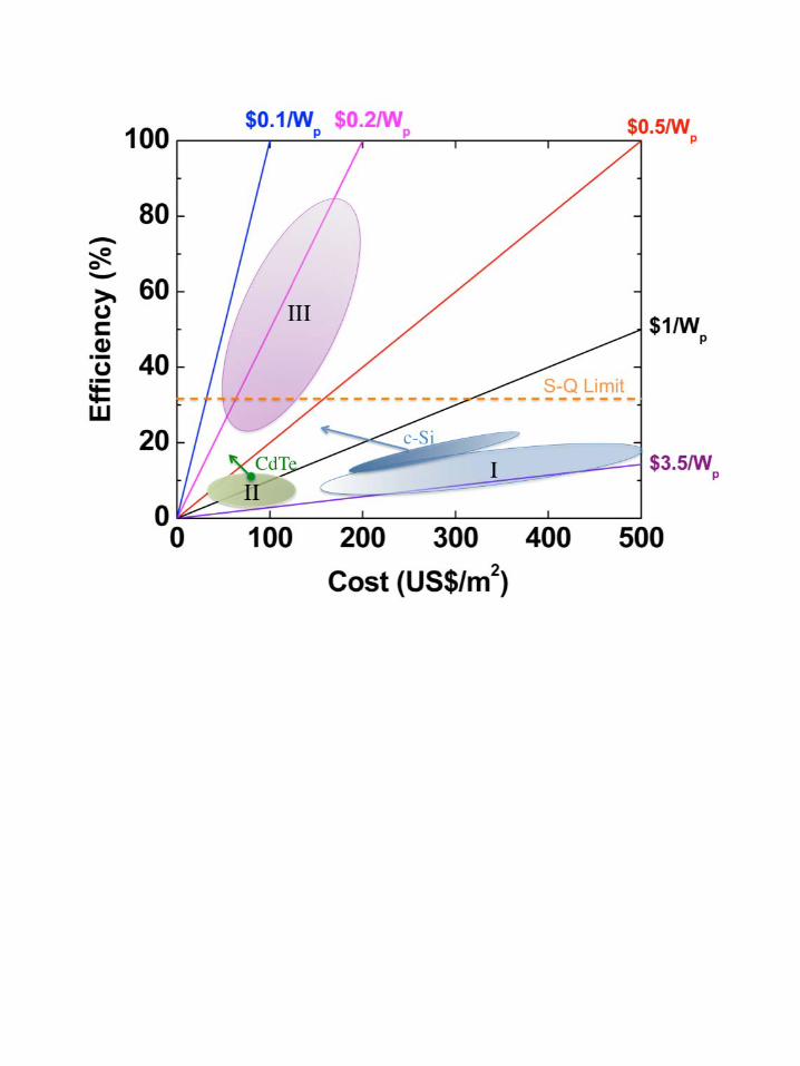
V. FUTURE OUTLOOK AND RECCOMENDATIONS
A. Redefining the boundaries of PV technologies
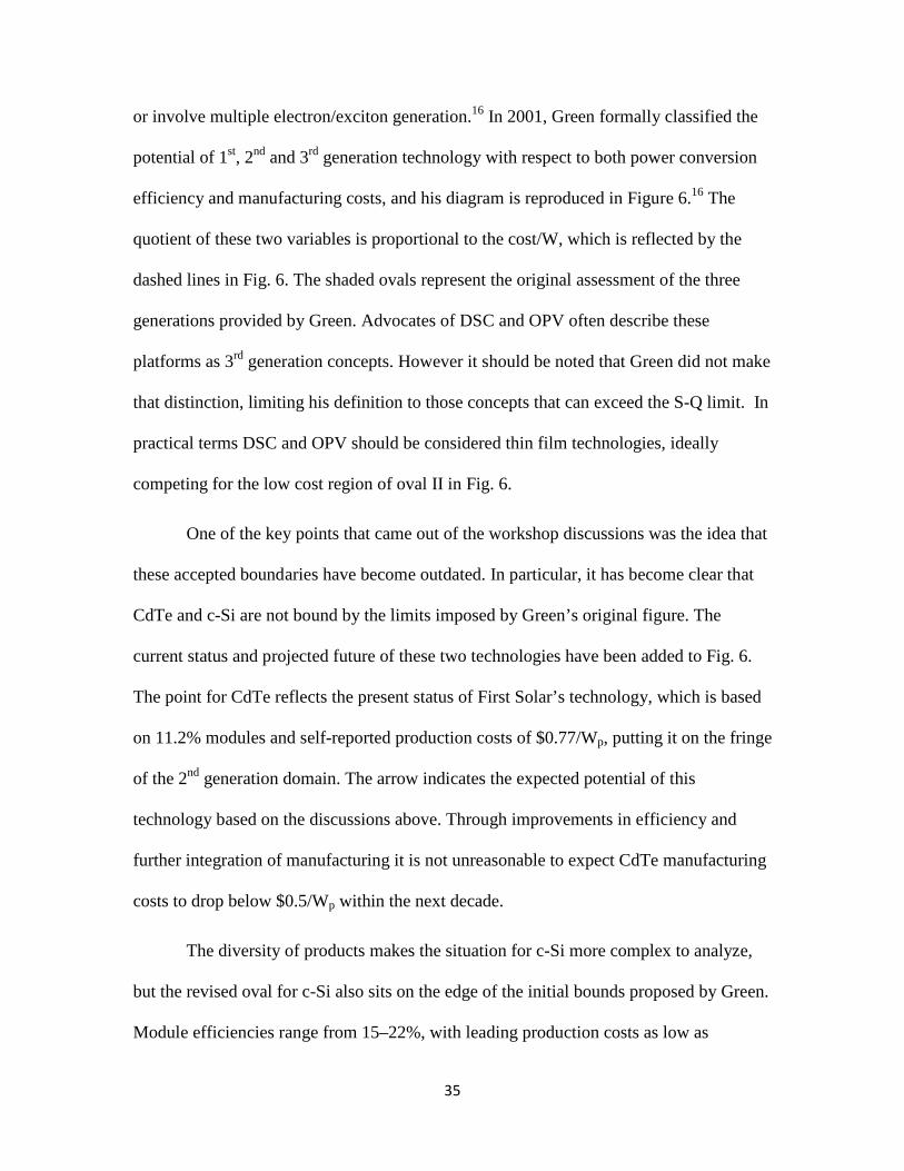
Photovoltaic technologies’ are often classified as being either 1st generation (c-
Si), 2nd generation (thin film), or 3rd generation concepts that have the potential to
overcome the S-Q limit such as devices that employ multi-junctions, extract hot carriers,
35
or involve multiple electron/exciton generation.16 In 2001, Green formally classified the
potential of 1st, 2nd and 3rd generation technology with respect to both power conversion
efficiency and manufacturing costs, and his diagram is reproduced in Figure 6.16 The
quotient of these two variables is proportional to the cost/W, which is reflected by the
dashed lines in Fig. 6. The shaded ovals represent the original assessment of the three
generations provided by Green. Advocates of DSC and OPV often describe these
platforms as 3rd generation concepts. However it should be noted that Green did not make
that distinction, limiting his definition to those concepts that can exceed the S-Q limit. In
practical terms DSC and OPV should be considered thin film technologies, ideally
competing for the low cost region of oval II in Fig. 6.
One of the key points that came out of the workshop discussions was the idea that
these accepted boundaries have become outdated. In particular, it has become clear that
CdTe and c-Si are not bound by the limits imposed by Green’s original figure. The
current status and projected future of these two technologies have been added to Fig. 6.
The point for CdTe reflects the present status of First Solar’s technology, which is based
on 11.2% modules and self-reported production costs of $0.77/Wp, putting it on the fringe
of the 2nd generation domain. The arrow indicates the expected potential of this
technology based on the discussions above. Through improvements in efficiency and
further integration of manufacturing it is not unreasonable to expect CdTe manufacturing
costs to drop below $0.5/Wp within the next decade.
The diversity of products makes the situation for c-Si more complex to analyze,
but the revised oval for c-Si also sits on the edge of the initial bounds proposed by Green.
Module efficiencies range from 15–22%, with leading production costs as low as
36
$1.10/Wp reported by Trina Solar in the second quarter of 2010. Again, the arrow leaving
the oval represents the future potential of this technology as discussed above. Here the
largest gains are related to further reduction in the productions costs through reduction in
Si requirements, as well as boosting module efficiency closer to 25%. This combination
provides a pathway that approaches $0.5/Wp. Some may find this projection overly
optimistic. However, one of the enlightening consequences of First Solar’s emergence
has been the ability of the x-Si industry to rapidly respond and reduce its costs. It is also
important to note that silicon does not have to move as far as CdTe. As module costs
drop below $1/Wp they become increasingly less important, as balance of systems issues
including inverters, racks, installation, and space become important cost drivers. These
costs drop with module efficiency, and thus silicon can afford to remain competitive
despite higher manufacturing costs than CdTe. It is too early to project what may happen
to CIGS, though it is plausible to expect that it might end up in a similar region, most
likely somewhere between CdTe and c-Si.
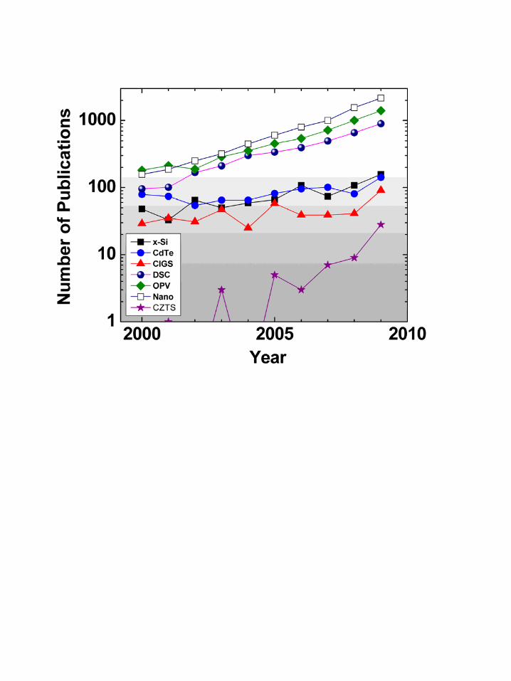
The discussion above on Green’s chart and PV classification is pertinent because
it has been highly influential on the overall landscape of research activity supported by
agencies such as NSF, the Department of Energy,143 and similar agencies around the
world. This can be quantified by examining the publication trends. In the past decade,
extensive resources have been invested in pursuing 3rd generation concepts, DSC, and
OPV. These investments are reflected by the number of publications in each subject.
Figure 7 displays on a semi-logarithmic scale the number of papers returned by Web of
Science each year in the past decade in response to a keyword search of “solar” + a
selected adjective. Any such study is imperfect, though alternative keywords
37
(photovoltaics, solar cells, etc.) yielded very similar results. The numbers reported here
are also in quite good agreement with those cited in reviews of individual
technologies.109, 128 The leading PV manufacturing technologies (c-Si, CdTe, CIGS) each
return only 60-100 pubs/year, and those numbers have remained essentially unchanged
over the past decade. In contrast, the interest in each of the next generation technologies
(DSC, OPV, nano*) has grown exponentially, expanding by an order of magnitude over
the past decade and currently averaging ~1500 pubs/year in each topic. This asymmetry
raises a red flag that many fundamental aspects of conventional technologies may not be
adequately investigated. This point was made salient at the workshop, where
representatives from thin film PV manufacturing companies lamented the dearth of
graduates ready for employment who are skilled in areas relevant to their needs. The
situation is not as bad in c-Si, which has benefited from crossover and displacement from
the IC industry.
There have been numerous scientific breakthroughs in the area of 3rd generation
PV,144-147 but practical devices are far from the point of commercialization.148, 149 In
general 3rd generation PV rely on the use of nanostructures such as quantum dots and
nanowires to generate the desired effects. A critical yet unresolved problem with devices
that employ such structures is that they will be dominated by interfaces. Interfaces are
integral to PV (the p-n junction), but their density should be minimized. Interfaces
typically serve as either recombination centers or barriers to charge transport, and the
demonstrated pathway to high efficiency has been through their elimination. Record
heteroepitaxial multi-junction cells are produced by molecular beam epitaxy.150 The
detrimental impact of interfaces is quite plainly seen by comparing the performance
38
within the silicon system (c-Si > mc-Si > nc-Si > a-Si). Likewise, record CdTe and CIGS
thin film devices are characterized by their large grain size.151
B. Cross-cutting areas for investment
Five challenges and topics that cut across the boundaries between the PV
technologies discussed above are discussed as areas that warrant additional research
investment.
1. Development of National User Facilities for Photovoltaic
Manufacturing Research
All PV technologies discussed here have matured to a point that future advances
will require simultaneous optimization of the many components that constitute a
complete solar cell. An innovative process or new material may have tremendous
intrinsic properties, but its value cannot be accurately assessed or fully exploited until
integrated into a complete device structure. This poses a major barrier for both small
business and university researchers alike, who most often cannot maintain the
infrastructure of a full solar line. User facilities that would provide robust process lines
on which researchers could test and develop their innovations is a critical link in the
technology development chain that is currently missing in the United States.
An excellent model that one might follow is the National Nanotechnology
Initiative (NNI), which involves multiple government agencies and has invested $14
billion USD over the past decade into building infrastructure to promote and facilitate
research, development, and technology transfer related to nanotechnology.152 Within the
NNI framework is an integrated partnership of fourteen user facilities, supported by NSF,
39
providing unparalleled opportunities for nanoscience and nanotechnology research. We
advocate that a similar investment be made in photovoltaic manufacturing science,
perhaps organized with facilities focused on individual process technologies. Such
facilities would dramatically accelerate the rate at which innovation can be harnessed to
meet the terawatt challenge. Such an investment would require a substantial
commitment, but it is fully justified in light of both the importance of sustainable energy
to humanity and the clear economic opportunities afforded by PV manufacturing.
2. Advanced photon management
The importance of this topic is self-evident as this phrase was used in conjunction
with the discussion of nearly every technology. Typically, advances and improvements in
efficiency involve materials that are applied externally to the cell, allowing them to be
developed independently without impacting cell designs that are highly optimized. This
decoupling is important because strategies and materials can be used in different
technologies. Specific topics within this area, in order of increasing complexity are as
follows.
1) Antireflection Coatings. Multi-layer or nanostructured antireflection coatings can
extend photon collection both across the spectrum and at diffuse angles beyond
normal incidence.153
2) Increasing the Path Length through the Absorber. Texturing, microstructures, or
nanostructure-based on plasmonics divert photons coming normal to the surface to
more oblique angles, increasing the path lengths of these photons through the
absorber and, thus, the probability of absorption.39
40
3) Optical field enhancement. Plasmonic enhancement of the optical field in the vicinity
of a metal nanoparticle is used to increase optical absorption and hence carrier
generation.154-156
4) Downshifting. This is the process of converting high-energy UV and blue photons,
and downconverting their energy to the middle of the visible spectrum where
quantum efficiency values typically approach 100%.157
5) Downconversion. Often called photon splitting, this is the process of transforming
one high energy photon into two photons that still have sufficient energy to create
electron-hole pairs.158
6) Upconversion. This is the reverse process whereby two low energy photons are
combined to produce one high energy photon that is capable of generating an
electron-hole pair.159, 160
These last two processes are a very long way from being practical, but provide
perhaps the best opportunity to truly surpass the S-Q limit by altering the solar spectrum
to produce a photon distribution that is more aligned with the requirements of a single
junction device.157
3. Can glass be replaced?
This is a simple but critical question. A detailed analysis of thin film
manufacturing suggested that under optimal conditions manufacturing costs could be
reduced to about $40 -50/m2 through economies of scale.107 It is not realistic to expect
costs to be any lower for any technology that requires the use of glass and a transparent
conducting oxide. A low cost, light-weight alternative that provides the same level of
41
transparency, protection, and thermal stability would be nothing short of revolutionary. A
positive answer to this question is essential if technologies such as OPV and DSC are to
become cost-competitive for principal power generation.
4. The science of manufacturing
With champion efficiencies nominally plateauing (Fig. 5), the continued
reductions in cost/Wp observed during the past decade has been due almost exclusively to
advances in manufacturing technology. Manufacturing and process development is often
overlooked as empirical knob turning, but there are many fundamental issues that have
not been addressed. Development of competitive manufacturing techniques requires
sophisticated modeling to understand how to maintain uniformity with respect to both
space and time. Accompanying this goal is the development of in-line diagnostics for real
time process control. The previous two topics presume a fundamental understanding of
how process conditions relate to materials chemistry and device performance, which
simply does not exist at a satisfactory level for the thin film technologies. Developments
in intelligent and potentially self-correcting control of process flow would help enable
and accelerate throughput volume.
5. Reliability science
An overlooked issue is that the economics of PV are predicated on sufficient
lifetimes, with targets traditionally of 20-30 years. Changes that improve efficiency are
only beneficial if they last. There are limited tools beyond standard lifetime testing that
can be used with any confidence to predict reliability. In part, this reflects the limited
knowledge with respect to the underlying mechanisms that are responsible for both cell
42
and module degradation. Improved understanding of these mechanisms and the
thermodynamics of their temporal evolution is necessary for all technologies and is
especially critical for the emerging approaches. New advances in diagnostic tools to
characterize structural and electronic changes as a device/module ages as well as models
that accurately describe and predict behavior would accelerate progress in these areas.
VI. SUMMARY AND CONCLUSIONS
Photovoltaics manufacturing has surpassed the 10 GW/yr production threshold
and is poised to accelerate as electricity production by PV reaches parity with
conventional electric power generation technologies later this decade. It is expected that
various forms of crystalline silicon will dominate the market for the foreseeable future.
Significant opportunities remain to improve 1st generation solar cells, mainly through
continued reduction of material requirements as well as additional improvements in
module efficiency. Thin film CdTe has established itself as a major player in the global
marketplace. Pending further improvements in efficiency, CdTe’s market share could
evolve to anywhere between 5 – 25%. After decades of being the leading thin film
technology, the prospects of amorphous silicon making a major contribution to the utility
sector appear constrained by high manufacturing costs and low efficiency. CIGS has
gained a foothold in PV manufacturing at ~100 MW/year, and the demonstrated potential
in efficiency provides reason for guarded optimism. The next five years will be critical
for CIGS to demonstrate robust manufacturing to allow it to break out and join CdTe as a
major player in the global PV market. Although encouraging progress has been made,
DSC and OPV are still limited at present by low efficiency and stability. Unless glass can
be replaced, costs will remain critically high, leaving them to compete with a-Si and
43
CIGS in niche applications requiring flexibility and/or low temperature processing. If
materials availability becomes a constraint at TW/year manufacturing levels it will likely
favor silicon-based technologies, though understudied systems like CZTS deserve
attention as their potential remains unknown. Fundamental challenges remain in 1st and
2nd generation PV technology, and additional investments in these areas are expected to
have the most immediate impact in meeting the challenge of sustainable electricity
production.
ACKNOWLEDGMENTS
This article is based upon the workshop supported by the National Science
Foundation through grant CBET-1027337. Any opinions, findings, and conclusions or
recommendations expressed in this material are those of the authors and do not
necessarily reflect the views of the National Science Foundation. The authors thank all of
the participants for their thoughtful contributions. C.A.W. acknowledges Science
Foundation Ireland for support through an E.T.S. Walton Visitor Fellowship during the
preparation of this manuscript. S.E.S would like to thank Russ Gaudiana (Konarka
Technologies) and Gang Li (Solarmer Energy) for insightful discussions. E. S. A.
acknowledges support by the National Science Foundation through grant CBET-
0931145.
References
1. M. I. Hoffert, K. Caldeira, A. K. Jain, E. F. Haites, L. D. D. Harvey, S. D. Potter,
M. E. Schlesinger, S. H. Schneider, R. G. Watts, T. M. L. Wigley and D. J.
Wuebbles, Nature 385, 881 (1998).
2. N. S. Lewis, Mater. Res. Bull. 32, 808 (2007).
3. D. Mills, Sol. Energy 76, 19 (2004).
44
4. J. R. Bolton, Science 202, 705 (1978).
5. P. V. Kamat, J. Phys. Chem. C 111, 2834 (2007).
6. T. Surek, J. Crystal Growth 275, 292 (2005).
7. C. A. Wolden. (2010). NSF PV Workshop Summary.
Available: http://inside.mines.edu/fs_home/cwolden/PVworkshop/Report2.html.
8. A. Goetzberger, C. Hebling and H. W. Schock, Mater. Sci. Eng. R 40, 1 (2003).
9. F. Aratani, Prog. Photovoltaics 13, 463 (2005).
10. K. Bullis, Technol. Rev. 113, 52 (2010).
11. S. Mehta, "2009 Global PV Cell and Module Production Analysis," GTM Research
2009.
12. P. Mints, Navigant Consulting Report, April, 2010.
13. M. A. Green, K. Emery, Y. Hishikawa and W. Warta, Prog. Photovoltaics 18, 346
(2010).
14. D. S. Kim, V. Yelundur, K. Nakayashiki, B. Rounsaville, V. Meemongkolkiat, A.
M. Gabor and A. Rohatgi, Sol. Energ Mat. Sol. C. 90, 1227 (2006).
15. Schott Solar, "EFG-Solar Cell Product Specification Sheet," May, 2010.
16. M. A. Green, Prog. Photovoltaics 9, 123 (2001).
17. W. Shockley and H. J. Queisser, J. Appl. Phys. 32, 510 (1961).
18. G. del Coso, I. Tobias, C. Canizo and A. Luque, J. Cryst. Growth 299, 165 (2007).
19. S. Pizzini, Sol. Energ Mat. Sol. C. 94, 1528 (2010).
20. M. Raugei, S. Bargigli and S. Ulgiati, Energy 32, 1310 (2007).
21. T. F. Ciszek, Mater. Res. Bull. 7, 731 (1972).
22. T. F. Ciszek, J. L. Hurd and M. Schietzelt, J. Electrochem. Soc. 129, 2838 (1982).
23. J. P. Kalejs, J. Cryst. Growth 230, 10 (2001).
24. A. G. Aberle, Sol. Energ Mat. Sol. C. 65, 239 (2001).
45
25. G. P. Smestad, Optoelectronics of Solar Cells. (SPIE Press, Bellingham, WA,
2002).
26. M. Wolf, San Diego, 1980 (unpublished).
27. M. J. Kerr, J. Schmidt & A. Cuevas, "Lifetime and efficiency limits of crystalline
silicon solar cells," in Proceedings of the 29th IEEE PVSC, New Orleans, 2002, p.
250.
28. M. A. Green, Prog. Photovoltaics 7, 327 (1999).
29. A. Luque, A. Cuevas and J. M. Ruiz, Sol. Cells 2, 151 (1980).
30. K. A. Munzer, K. T. Holdermann, R. E. Schlosser and S. Sterk, IEEE Trans.
Electron. Dev. 46, 2055 (1999).
31. V. Depauw, I. Gordon, G. Beaucarne, J. Poortmans, R. Mertens and J. P. Celis, J.
Appl. Phys. 106, 033516 (2009).
32. M. L. Terry, A. Straub, D. Inns, D. Y. Song and A. G. Aberle, Appl. Phys. Lett. 86,
172108 (2005).
33. D. Y. Song, D. Inns, A. Straub, M. L. Terry, P. Campbell and A. G. Aberle, Thin
Solid Films 513, 356 (2006).
34. F. Dross, J. Robbelein, B. Vandevelde, E. Van Kerschaver, I. Gordon, G. Beaucarne
and J. Poortmans, Appl. Phys. A-Mater. 89, 149 (2007).
35. C. Podewils, Photon International May, 116 (2009).
36. M. J. Kerr and A. Cuevas, Semicond. Sci. Tech. 17, 35 (2002).
37. J. Schmidt, A. Merkle, R. Brendel, B. Hoex, M. C. M. van de Sanden and W. M. M.
Kessels, Prog. Photovoltaics 16, 461 (2008).
38. D. Shir, J. Yoon, D. Chanda, J. H. Ryu and J. A. Rogers, Nano Lett. 10, 3041
(2010).
39. S. Pillai and M. A. Green, Sol. Energ Mat. Sol. C. 94, 1481 (2010).
40. P. C. Rowlette and C. A. Wolden, ACS Appl. Mater. Interfaces 1, 2586 (2009).
41. S. Eglash, Laser Focus World 45, 39 (2009).
46
42. P. Engelharet, S. Hermann, T. Neubere, H. Plagwitz, R. Grischke, R. Meyd, U.
Klug, A. Schoonderbeek, U. Stute and R. Brendel, Prog. Photovoltaics 15, 521
(2007).
43. D. A. Cusano, Solid-State Electron. 6, 217 (1963).
44. C. Ferekides and J. Britt, Appl. Phys. Lett. 62, 2851 (1993).
45. R. F. Brebrick and A. J. Strauss, J. Phys. Chem. Solids 25, 1441 (1964).
46. J. M. Kestner, S. McElvain, S. Kelly, L. M. Woods, T. R. Ohno and C. A. Wolden,
Sol. Energ Mat. Sol. C. 83, 55 (2004).
47. P. V. Meyers and S. P. Albright, Prog. Photovoltaics 8, 161 (2000).
48. X. Wu, Sol. Energy 77, 803 (2004).
49. A. D. Compaan, A. Gupta, S. Lee, S. Wang and J. Drayton, Sol. Energy 77, 815
(2004).
50. X. Wu, S. Asher, D. H. Levi, D. E. King, Y. Yan, T. A. Gessert and P. Sheldon, J.
Appl. Phys. 89, 4564 (2001).
51. N. Naghavi, D. Abou-Ras, N. Allsop, N. Barreau, S. Bucheler, A. Ennaoui, C. H.
Fischer, C. Guillen, D. Hariskos, J. Herrero, R. Klenk, K. Kushiya, D. Lincot, R.
Menner, T. Nakada, C. Platzer-Bjorkman, S. Spiering, A. N. Tiwari and T.
Torndahl, Prog. Photovoltaics 18, 411 (2010).
52. D. W. Niles, G. Herdt and M. AlJassim, J. Appl. Phys. 81, 1978 (1997).
53. M. A. Hernandez-Fenollosa, D. P. Halliday, K. Durose, M. D. Campo and J. Beier,
Thin Solid Films 431, 176 (2003).
54. M. Carmody, S. Mallick, J. Margetis, R. Kodama, T. Biegala, D. Xu, P. Bechmann,
J. W. Garland and S. Sivananthan, Appl. Phys. Lett. 96, 153502 (2010).
55. W. K. Metzger, I. L. Repins and M. A. Contreras, Appl. Phys. Lett. 93, 022110
(2008).
56. J. Sites and J. Pan, Thin Solid Films 515, 6099 (2007).
57. M. Beck, Personal Communication, NSF PV Workshop, May, 2010.
47
58. M. A. Green, "Learning experience for thin-film solar modules: First Solar, Inc.
case study", Prog. Photovoltaics, in press (2011).
59. D. Cahen and R. Noufi, Sol. Cells 30, 53 (1991).
60. H. R. Moutinho, M. M. Al-Jassim, D. H. Levi, P. C. Dippo and L. L. Kazmerski, J.
Vac. Sci. Technol. A 16, 1251 (1998).
61. D. Grecu and A. D. Compaan, Appl. Phys. Lett. 75, 361 (1999).
62. Y. Yan, D. Albin and M. M. Al-Jassim, Appl. Phys. Lett. 78, 171 (2001).
63. S. Erra, C. Shivakumar, H. Zhao, K. Barri, D. L. Morel and C. S. Ferekides, Thin
Solid Films 515, 5833 (2007).
64. T. A. Gessert, S. Asher, S. Johnston, M. Young, P. Dippo and C. Corwine, Thin
Solid Films 515, 6103 (2007).
65. V. M. Fthenakis, M. Fuhrmann, J. Heiser, A. Lanzirotti, J. Fitts and W. Wang, Prog.
Photovoltaics 13, 713 (2005).
66. H. Steinberger, Prog. Photovoltaics 6, 99 (1998).
67. D. E. Carlson and C. R. Wronski, Appl. Phys. Lett. 28, 671 (1976).
68. A. H. Mahan, Y. Xu, E. Iwaniczko, D. L. Williamson, B. P. Nelson and Q. Wang, J.
Non-Cryst. Solids 299-302, 2 (2002).
69. A. V. Shah, H. Schade, M. Vanecek, J. Meier, E. Vallat-Sauvain, N. Wyrsch, U.
Kroll, C. Droz and J. Bailat, Prog. Photovoltaics 12, 113 (2004).
70. D. L. Staebler and C. R. Wronski, Appl. Phys. Lett. 31, 292 (1977).
71. S. Veprek and V. Marecek, Solid-State Electron. 11, 683 (1968).
72. A. Shah, J. Meier, E. Vallat-Sauvain, C. Droz, U. Kroll, N. Wyrsch, J. Guillet and
U. Graf, Thin Solid Films 403-404, 179 (2002).
73. J. Yang, A. Banerjee and S. Guha, Appl. Phys. Lett. 70, 2975 (1997).
74. M. Taguchi, H. Sakata, Y. Yoshimine, E. Maruyama, A. Terakawa, M. Tanaka and
S. Kiyama, "An approach for the higher efficiency in the HIT cells," in Conference
Record of the 31st IEEE Photovoltaic Specialists Conference, 2005, pp. 866-871.
48
75. A. Poruba, A. Fejfar, Z. Remes, J. Springer, M. Vanecek, J. Kocka, J. Meier, P.
Torres and A. Shah, J. Appl. Phys. 88, 148 (2000).
76. T. Roschek, T. Repmann, J. Muller, B. Rech and H. Wagner, J. Vac. Sci. Technol.
A 20, 492 (2002).
77. M. Fukawa, S. Suzuki, L. H. Guo, M. Kondo and A. Matsuda, Sol. Energ. Mat. Sol.
C. 66, 217 (2001).
78. Y. Mai, S. Klein, R. Carius, J. Wolff, A. Lambertz, F. Finger and X. Geng, J. Appl.
Phys. 97, 114913 (2005).
79. J. Rudiger, H. Brechtel, A. Kottwitz, J. Kuske and U. Stephan, Thin Solid Films
427, 16 (2003).
80. M. N. van den Donker, B. Rech, F. Finger, W. M. M. Kessels and M. C. M. van de
Sanden, Appl. Phys. Lett. 87, 263503 (2005).
81. L. L. Kazmerski, F. R. White and G. K. Morgan, Appl. Phys. Lett. 29, 268 (1976).
82. J. H. L. Stolt, J. Kessler, M. Ruckh, K.-O. Velthaus, ans H.-W. Schock, Appl. Phys.
Lett. 62, 597 (1993).
83. A. M. Gabor, J. R. Tuttle, D. S. Albin, M. A. Contreras, R. Noufi and A. M.
Herman, Appl. Phys. Lett. 65, 198 (1994).
84. T. Anegawa, Y. Oda, T. Minemoto and H. Takakura, J. Cryst. Growth 311, 742
(2009).
85. A. N. Tiwari, D. Lincot and M. Contreras, Prog. Photovoltaics 18, 389 (2010).
86. S. Niki, M. Contreras, I. Repins, M. Powalla, K. Kushiya, S. Ishizuka and K.
Matsubara, Prog. Photovoltaics 18, 453 (2010).
87. M. A. Contreras, B. Egaas, K. Ramanathan, J. Hiltner, F. Hasoon and R. Noufi,
Prog. Photovoltaics 7, 311 (1999).
88. K. Ramanathan, G. Teeter, J. C. Keane and R. Noufi, Thin Solid Films 480, 499
(2005).
49
89. R. Scheer, A. Pérez-Rodríguez and W. K. Metzger, Prog. Photovoltaics 18, 467
(2010).
90. C. J. Hibberd, E. Chassaing, W. Liu, D. B. Mitzi, D. Lincot and A. N. Tiwari, Prog.
Photovoltaics 18, 434 (2010).
91. R. N. Bhattacharya, J. Electrochem. Soc. 130, 2040 (1983).
92. D. Lincot, J. F. Guillemoles, S. Taunier, D. Guimard, J. Sicx-Kurdi, A. Chaumont,
O. Roussel, O. Ramdani, C. Hubert, J. P. Fauvarque, N. Bodereau, L. Parissi, P.
Panheleux, P. Fanouillere, N. Naghavi, P. P. Grand, M. Benfarah, P. Mogensen and
O. Kerrec, Sol. Energy 77, 725 (2004).
93. M. G. Panthani, V. Akhavan, B. Goodfellow, J. P. Schmidtke, L. Dunn, A.
Dodabalapur, P. F. Barbara and B. A. Korgel, J. Am. Chem. Soc. 130, 16770
(2008).
94. M. Kaelin, D. Rudmann, F. Kurdesau, T. Meyer, H. Zogg and A. N. Tiwari, Thin
Solid Films 431-432, 58 (2003).
95. V. K. Kapur, B. M. Basol and E. S. Tseng, Sol. Cells 21, 65 (1987).
96. V. K. Kapur, A. Bansal, P. Le and O. I. Asensio, Thin Solid Films 431-432, 53
(2003).
97. J. van Duren, D. Jackrel, F. Jacob, C. Leidholm, A. Pudov, M. Robinson & Y.
Roussillon, "The next generation in thin film photovoltaic process technology," in
Conference Record of the Seventeenth International Photovoltaic Science and
Engineering Conference, Fukuoka, Japan, 2007.
98. D. B. Mitzi, Adv. Mater. 21, 3141 (2009).
99. W. Liu, D. B. Mitzi, M. Yuan, A. J. Kellock, S. J. Chey and O. Gunawan, Chem.
Mater. 22, 1010 (2010).
100. S. Siebentritt, M. Igalson, C. Persson and S. Lany, Prog. Photovoltaics 18, 390
(2010).
101. G. L. Graff, R. E. Williford and P. E. Burrows, J. Appl. Phys. 96, 1840 (2004).
50
102. B. A. Andersson, Prog. Photovolt: Res. Appl. 8, 61 (2000).
103. M. A. Green, Prog. Photovolt.: Res. Appl. 17, 347 (2009).
104. C. Wadia, A. P. Alivisatos and D. M. Kammen, Environ. Sci. Technol. 43, 2072
(2009).
105. V. Fthenakis, Renew. Sustain. Energy Rev. 13, 2746 (2009).
106. K. Zweibel, Science 328, 699 (2010).
107. K. Zweibel, Sol. Energ Mat. Sol. C. 63, 375 (2000).
108. B. O'Regan and M. Gratzel, Nature 353, 737 (1991).
109. A. Hagfeldt, G. Boschloo, L. Sun, L. Kloo and H. Pettersson, Chem. Rev. 110,
6595 (2010).
110. M. K. Nazeeruddin, A. Kay, I. Rodicio, R. Humphry-Baker, E. Mueller, P. Liska,
N. Vlachopoulos and M. Graetzel, J. Am. Chem. Soc. 115, 6382 (1993).
111. G. E. Tulloch, J. Photochem. Photobiol. A: Chem. 164, 209 (2004).
112. T. W. Hamann, R. A. Jensen, A. B. F. Martinson, H. Van Ryswyk and J. T. Hupp,
Energy Environ. Sci. 1, 66 (2008).
113. R. Harikisun and H. Desilvestro, Solar Energy In Press, Corrected Proof.
114. N. Kato, K. Higuchi, H. Tanaka, J. Nakajima, T. Sano and T. Toyoda, Sol. Energ.
Mat. Sol. C. 95, 301 (2011).
115. C. J. Brabec, S. Gowrisanker, J. J. M. Halls, D. Laird, S. J. Jia and S. P. Williams,
Adv. Mater. 22, 3839 (2010).
116. Heliatek. (12/1/10). Available: http://www.heliatek.com/news-19
117. Konarka. (12/1/10).
Available:
118. C. W. Tang, Appl. Phys. Lett. 48, 183 (1986).
http://www.konarka.com/index.php/newsroom/press-release-list/
119. M. S. White, D. C. Olson, S. E. Shaheen, N. Kopidakis and D. S. Ginley, Appl.
Phys. Lett. 89, 143517 (2006).
51
120. S. K. Hau, H. L. Yip and A. K. Y. Jen, Polym. Rev. 50, 474 (2010).
121. C. Tao, S. Ruan, G. Xie, X. Kong, L. Shen, F. Meng, C. Liu, X. Zhang, W. Dong
and W. Chen, Appl. Phys. Lett. 94, 043311 (2009).
122. M. Riede and et al., Nanotechnology 19, 424001 (2008).
123. H. Spanggaard and F. C. Krebs, Sol. Energ. Mat. Sol. C. 83, 125 (2004).
124. E. Bundgaard and F. C. Krebs, Sol. Energ. Mat. Sol. C. 91, 954 (2007).
125. R. Kroon, M. Lenes, J. C. Hummelen, P. W. M. Blom and B. d. Boer, Polym. Rev.
48, 531 (2008).
126. M. J. Currie, J. K. Mapel, T. D. Heidel, S. Goffri and M. A. Baldo, Science 321,
226 (2008).
127. D. Veldman, S. C. J. Meskers and R. A. J. Janssen, Adv. Funct. Mater. 19, 1939
(2009).
128. T. Ameri, G. Dennler, C. Lungenschmied and C. J. Brabec, Energy Environ. Sci. 2,
347 (2009).
129. A. Anctil, C. Babbit, B. Landi and R. P. Raffaelle, presented at the 35th IEEE
Photovoltaic Specialist Conference, Honolulu, Hawaii, 2010 (unpublished).
130. R. García-Valverde, J. A. Cherni and A. Urbina, Prog. Photovoltaics 18, 535
(2010).
131. J. Kalowekamo and E. Baker, Sol. Energy 83, 1224 (2009).
132. R. Tipnis, J. Bernkopf, S. J. Jia, J. Krieg, S. Li, M. Storch and D. Laird, Sol. Energ.
Mat. Sol. C. 93, 442 (2009).
133. V. Shrotriya, Nat. Photon. 3, 447 (2009).
134. M. Jørgensen, K. Norrman and F. C. Krebs, Sol. Energ. Mat. Sol. C. 92, 686
(2008).
135. A. O. Musa, T. Akomolafe and M. J. Carter, Sol. Energ. Mat. Sol. C. 51, 305
(1998).
52
136. A. Ennaoui, S. Fiechter, C. Pettenkofer, N. Alonsovante, K. Buker, M. Bronold, C.
Hopfner and H. Tributsch, Sol. Energ. Mat. Sol. C. 29, 289 (1993).
137. H. Katagiri, Thin Solid Films 480, 426 (2005).
138. H. Katagiri, K. Saitoh, T. Washio, H. Shinohara, T. Kurumadani and S. Miyajima,
Sol. Energ. Mat. Sol. C. 65, 141 (2001).
139. K. Oishi, G. Saito, K. Ebina, M. Nagahashi, K. Jimbo, W. S. Maw, H. Katagiri, M.
Yamazaki, H. Araki and A. Takeuchi, Thin Solid Films 517, 1449 (2008).
140. Q. J. Guo, H. W. Hillhouse and R. Agrawal, J. Am. Chem. Soc. 131, 11672 (2009).
141. C. Steinhagen, M. G. Panthani, V. Akhavan, B. Goodfellow, B. Koo and B. A.
Korgel, J. Am. Chem. Soc. 131, 12554 (2009).
142. T. K. Todorov, K. B. Reuter and D. B. Mitzi, Adv. Mater. 22, E156 (2010).
143. "Basic Research Needs for Solar Energy Utilization," U.S. Department of Energy Report, (2005).
144. R. D. Schaller and V. I. Klimov, Phys.Rev. Lett. 92, 186601 (2004).
145. A. J. Nozik, Chem. Phys. Lett. 457, 3 (2008).
146. W. A. Tisdale, K. J. Williams, B. A. Timp, D. J. Norris, E. S. Aydil and X.-Y. Zhu,
Science 328, 1543 (2010).
147. J. B. Sambur, T. Novet and B. A. Parkinson, Science 330, 63 (2010).
148. J. M. Luther, M. Law, M. C. Beard, Q. Song, M. O. Reese, R. J. Ellingson and A. J.
Nozik, Nano Lett. 8, 3488 (2008).
149. Y. Wu, C. Wadia, W. L. Ma, B. Sadtler and A. P. Alivisatos, Nano Lett. 8, 2551
(2008).
150. J. F. Geisz, S. Kurtz, M. W. Wanlass, J. S. Ward, A. Duda, D. J. Friedman, J. M.
Olson, W. E. McMahon, T. E. Moriarty and J. T. Kiehl, Appl. Phys. Lett. 91
(2007).
151. J. D. Beach and B. E. McCandless, Mater. Res. Bull. 32, 225 (2007).
53
152. National Nanotechnology Initiative - 2011 Budget Supplement,
Available: http://www.nano.gov/NNI_2011_budget_supplement.pdf, (2010).
153. S. Chhajed, M. F. Schubert, J. K. Kim and E. F. Schubert, Appl. Phys. Lett. 93,
251108 (2008).
154. K. Tanabe, Energies 2, 504 (2009).
155. B. P. Rand, P. Peumans and S. R. Forrest, J. Appl. Phys. 96, 7519 (2004).
156. A. J. Morfa, K. L. Rowlen, T. H. Reilly, Iii, M. J. Romero and J. van de Lagemaat,
Appl. Phys. Lett. 92, 013504 (2008).
157. C. Strumpel, M. McCann, G. Beaucarne, V. Arkhipov, A. Slaoui, V. Svrcek, C. del
Canizo and I. Tobias, Sol. Energ. Mat. Sol. C. 91, 238 (2007).
158. D. Timmerman, I. Izeddin, P. Stallinga, I. N. Yassievich and T. Gregorkiewicz, Nat.
Photonics 2, 105 (2008).
159. T. Trupke, M. A. Green and P. Wurfel, J. Appl. Phys. 92, 4117 (2002).
160. F. Auzel, Chem. Rev. 104, 139 (2003).
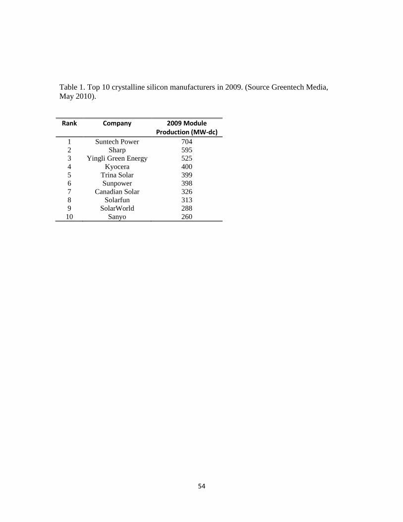
54
Table 1. Top 10 crystalline silicon manufacturers in 2009. (Source Greentech Media, May 2010).
Rank Company 2009 Module Production (MW-dc)
1 Suntech Power 704 2 Sharp 595 3 Yingli Green Energy 525 4 Kyocera 400 5 Trina Solar 399 6 Sunpower 398 7 Canadian Solar 326 8 Solarfun 313 9 SolarWorld 288
10 Sanyo 260
55
Figure Captions
Figure 1. (Color online) Projected convergence of the cost of electricity produced by PV
and the conventional grid prices.
Figure 2. (Color online) Workshop demographics.
Figure 3. (Color online) Market size and the share held by relevant technologies in 2008
and 2009.
Figure 4. (Color online) Champion efficiencies reported for cells and commercial
modules for the established PV manufacturing technologies.
Figure 5. (Color online) The evolution of champion cell efficiencies since 1995 for
various PV technologies.
Figure 6. (Color online) Green’s 2001 classification of PV technologies superimposed
with the current status (solid) and projected evolution (arrows) of c-Si and CdTe
technologies.
Figure 7. (Color online) The number of papers returned on Web of Science each year in
response to a search of “solar” + the individual keywords listed in the figure legend (c-Si
= "crystalline silicon”).