pen-on-paper flexible ...lewisgroup.seas.harvard.edu/files/lewisgroup/files/russo_advmat... ·...
TRANSCRIPT

3426
www.advmat.dewww.MaterialsViews.com
CO
MM
UN
ICATI
ON
Analisa Russo , Bok Yeop Ahn , Jacob J. Adams , Eric B. Duoss , Jennifer T. Bernhard , and Jennifer A. Lewis*
Pen-on-Paper Flexible Electronics
Figure 1 . a) Optical image of a rollerball pen loaded with a conductive silver ink. The background shows conductive text written on Xerox paper. b and c) SEM images of the side and top views of the rollerball pen. d) Optical image of the rollerball pen tip, captured during writing a con-ductive silver track on a Xerox paper.
Printed electronics constitute an emerging class of materials with potential application in photovoltaics, [ 1 ] transistors, [ 2 , 3 ] dis-plays, [ 4–6 ] batteries, [ 7 ] antennas, [ 8 ] and sensors. [ 9 , 10 ] Recent atten-tion has focused on paper substrates as a low-cost, enabling platform for fl exible, lightweight, and disposable devices. [ 11–13 ] Such devices require conductive electrodes, which, to date, have been deposited by sputter coating, [ 14 ] inkjet printing, [ 15 ] and airbrush spraying. [ 11 ] However, these deposition methods are either costly or employ dilute inks that readily permeate the paper substrate. Here, we demonstrate a facile pen-on-paper approach for creating fl exible printed electronics. Using a roll-erball pen fi lled with conductive silver ink, we directly write conductive text, electronic art, interconnects for light emitting diode (LED) arrays, and three-dimensional (3D) antennas on paper.
Paper substrates offer many advantages for printed electronic devices. Not only is paper widely available and inexpensive, it is lightweight, biodegradable, and can be rolled or folded into 3D confi gurations. Functional electronic components, including thermochromic displays, [ 14 ] disposable radio frequency identi-fi cation (RFID) tags, [ 16 , 17 ] and cellulose-based batteries, [ 18 ] have recently been produced on paper substrates. The wide variety of available paper textures, compositions, and coatings can be exploited to enable specifi c device architectures. For example, highly absorbent paper is suitable for disposable microfl uidic and diagnostic devices, [ 19 ] whereas smooth photo-quality paper is used for coloured electrowetting pixels. [ 20 ] Facile routes to cre-ating devices “on-the-fl y” under ambient conditions are needed to fully exploit the potential of paper-based printed electronics.
© 2011 WILEY-VCH Verlag wileyonlinelibrary.com
A. Russo ,[ + + ] Dr. B. Y. Ahn ,[ + + ] Dr. E. B. Duoss, [ + ] Prof. J. A. Lewis Department of Materials Science and EngineeringUniversity of Illinois at Urbana-ChampaignUrbana, IL 61801, USAE-mail: [email protected] Prof. J. A. Lewis Department of Chemical and Biomolecular EngineeringUniversity of Illinois at Urbana-ChampaignUrbana, IL 61801, USA Dr. J. J. Adams , Prof. J. T. Bernhard Electromagnetics LaboratoryDepartment of Electrical and Computer EngineeringUniversity of Illinois at Urbana-ChampaignUrbana, IL 61801, USA [ + ] Present address: Center for Micro- and Nanotechnology, Lawrence Livermore National Laboratory, Livermore, CA 94551, USA [ + + ] A.R. and B.Y.A. contributed equally to this work.
DOI: 10.1002/adma.201101328
The pen-on-paper (PoP) paradigm offers a unique approach to fabricating fl exible devices by using a patterning instrument that is itself as ubiquitous and portable as the paper substrate. Rollerball pens are especially well suited for dispensing con-ductive inks due to their compatibility with liquids and gels. [ 21 ] Pens with ball diameters ranging from 250 μ m to nearly a milli meter are commercially available and are specifi cally engi-neered for precision writing on paper. Figure 1 a–c shows a rep-resentative rollerball pen with a ball diameter ( d ) of 960 μ m that is fi lled with colloidal silver ink for writing conductive features on Xerox paper. In this example, conductive text is printed with features that are approximately 650 μ m wide (Figure 1 d).
Central to the PoP approach is the design of a silver ink that readily fl ows through the rollerball pen tip during writing, does not leak from, dry out, or coagulate within the pen, and is con-ductive upon printing under ambient conditions. To create an ink with these attributes, we synthesized silver particles in an aqueous solution by reducing silver nitrate in the presence of a surface capping agent, poly(acrylic acid) (PAA) and dieth-anolamine. [ 22–26 ] Using a multistep procedure, we fi rst mixed these components to create a population of silver nanoparticles ( ∼ 5 nm in diameter). This particle population is then ripened by heating the solution to 65 ° C for 1.5 h to yield a mean dia-meter of 400 ± 120 nm, as shown in Figure 2 a. Ethanol, a poor solvent for the PAA-coated particles, is added to induce rapid coagulation and then the precipitate is centrifuged to achieve high solids loading. The silver particles are redispersed in water
GmbH & Co. KGaA, Weinheim Adv. Mater. 2011, 23, 3426–3430

www.advmat.dewww.MaterialsViews.com
CO
MM
UN
ICATIO
N
Figure 2 . a) TEM image of the synthesized silver particles and optical image of a representative ink (inset). b) Apparent ink viscosity ( η ) measured at 1 s − 1 as a function of silver content. The shaded region indicates optimal ink formulations for printing using a 960 μ m diameter rollerball tip. c) Electrical resistivity of the silver inks (50 wt% silver) as-printed at 25 ° C and as a function of annealing temperature and time.
to remove the PAA capping agent, which is initially present at 10% by weight of silver, and again concentrated by centrifuga-tion. This process is repeated three times, resulting in com-plete removal of PAA (see Supporting Information, Figure S1). Finally, hydroxyethyl cellulose (HEC), a viscosifi er, is added to tailor the ink rheology.
Figure 2 b shows the apparent viscosity ( η ) acquired at a shear rate of 1 s − 1 as a function of solids loading for silver inks pre-pared with an HEC:Ag ratio of 3 wt%. The apparent viscosity is ∼ 0.3 Pa · s for the inks containing 35 wt% silver particles. How-ever, the viscosity increases by three orders of magnitude for inks composed of 65 wt% silver particles. Over this composi-tional range, each ink exhibits shear thinning behavior, which is most pronounced at the highest solids loading (see Sup-porting Information, Figure S2). Of these compositions, only those inks with 45–55 wt% silver particles and, hence, viscosi-ties of 1–10 Pa · s reliably fl ow through the ballpoint tip without leaking, skipping, or clogging. Notably, these inks are stable for months when stored in properly sealed containers and can fl ow through rollerball pens with diameters as small as 250 μ m (see Supporting Information, Figure S3). In addition, these inks can be written on both soft and rigid substrates, including polymer fi lms, wood, and ceramics by this PoP approach (see Supporting Information, Figure S4).
Figure 2 c shows the electrical resistivity of the silver ink (50 wt% silver) after printing and drying under ambient condi-tions (25 ° C) and as a function of annealing temperature and time. To precisely control the sample dimensions, silver fi lms (1 cm × 1 cm wide, 12 μ m in height) are formed by doctor blading the ink on a glass substrate. The ink is conductive after drying at room temperature for 30 min, exhibiting an electrical resistivity of 1.99 × 10 − 4 Ω · cm. Upon annealing at 110 ° C, a slight decrease in resistivity is observed likely due to evaporation of residual solvent. Annealing to higher temperatures ( ≥ 170 ° C) results in a signifi cant decrease in the electrical resistivity (4.34 × 10 − 6 Ω · cm) as particle sintering ensues. Corresponding images of the microstructural evolution observed during annealing are provided as the supplementary information (Figure S5). Impor-tantly, the printed inks exhibit an electrical resistivity that is
© 2011 WILEY-VCH Verlag GAdv. Mater. 2011, 23, 3426–3430
several orders of magnitude below that observed for silver nano-particle inks (mean diameter = 20 ± 5 nm) previously developed for omnidirectional printing of fl exible, stretchable, and span-ning electrodes. [ 22 ] Their greatly enhanced electrical perform-ance likely arises due to removal of the PAA capping layer from the silver particle surfaces as well as their larger mean particle size. This ability to directly write conductive features under ambient conditions is essential for the PoP approach.
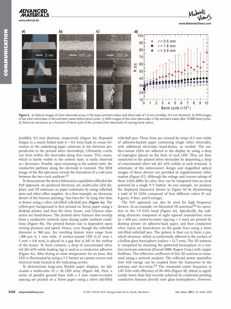
To investigate the mechanical fl exibility of the printed fea-tures, we produced a linear array of 5 silver electrodes (width = 620 μ m, height = ∼ 20 μ m, and length = 1.5 cm) spaced 1.5 mm apart using a 960 μ m roller ball pen fi lled with colloidal silver ink (50 wt% silver) on Xerox paper and dried at room tem-perature for 24 h in air. The silver ink conformally coats the fi brous paper surface, exhibiting good adhesion as confi rmed by the ASTM D3330 tape test. The electrode-patterned paper substrates are actuated between the fl at and bent states at a bending rate of 2 cm s − 1 to a specifi ed minimum bend radius using a custom-built mechanical stage coupled to a computer-controlled 3-axis micropositioning system (see Supporting Information, Figure S6). Optical images of the test specimens at minimum bend radii ( r ) of 2.9 mm, 1.6 mm, and 0.5 mm are shown in Figure 3 a. Corresponding scanning electron images reveal that there is no noticeable crack formation or delami-nation during the fi rst bend cycle (Figure 3 b). We measured the electrical resistance ( R ) as a function of bend radius and number of bend cycles, and average R values obtained from the fi ve electrodes are reported in Figure 3 d. For r of 2.9 mm and 1.6 mm, the silver electrodes exhibit a robust response over 10 000 bending cycles with a slight increase in their respec-tive electrical resistance of 1.2 and 1.6 relative to their initial, as-printed state. For the most extreme bend radius of 0.5 mm, the electrical resistance increases gradually after many cycles. Two electrodes undergo cracking and fail after 6000 cycles, while three electrodes survive after 10 000 cycles exhibiting a 3.2-fold increase in their electrical resistance relative to their initial, as-printed state. After 10 000 cycles at a bend radius of 0.5 mm, their microstructure is observed by SEM in both fl at (top) and bent confi gurations, with bend radii of 1.6 mm
3427mbH & Co. KGaA, Weinheim wileyonlinelibrary.com
342
www.advmat.dewww.MaterialsViews.com
CO
MM
UN
ICATI
ON
Figure 3 . a) Optical images of silver electrode arrays in fl at (top) and bent states with bend radii of 1.6 mm (middle), 0.5 mm (bottom). b) SEM images of the silver electrodes in fl at and bent states before bend cycles. c) SEM images of the silver electrodes in fl at and bent states after 10 000 bend cycles. d) Electrical resistance as a function of bend cycle of the printed silver electrodes of varying bend radius.
(middle), 0.5 mm (bottom), respectively (Figure 3 c). Repeated fatigue in a nearly folded state ( r = 0.5 mm) leads to crease for-mation in the underlying paper substrate in the direction per-pendicular to the printed silver electrode(s). Ultimately, cracks can form within the electrodes along this crease. This crease, which is barely visible in the unbent state, is easily observed as r decreases. Notably, upon returning to the unbent state, the conductive pathway along the electrode is restored. The SEM image of the fl at specimen reveals the formation of a cold joint between the two crack surfaces. [ 27 ]
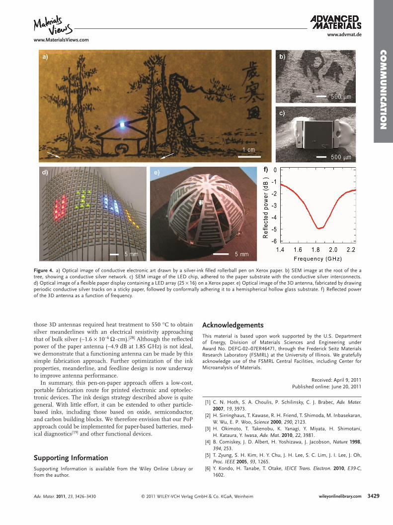
To demonstrate the device fabrication capabilities afforded the PoP approach, we produced electronic art, multi-color LED dis-plays, and 3D antennas on paper substrates by using rollerball pens and other offi ce supplies. As a fi rst example, an electronic sketch of the famous painting “Sae-Han-Do” by Jung Hee Kim is drawn using a silver ink-fi lled rollerball pen ( Figure 4 a). The yellow-grey background is fi rst printed on Xerox paper using a desktop printer, and then the trees, house, and Chinese char-acters are hand-drawn. The printed silver features that overlap form a conductive network upon drying under ambient condi-tions (Figure 4 b). The printed feature size is dependent upon writing pressure and speed. Hence, even though the rollerball diameter is 960 μ m, the resulting feature sizes range from ∼ 300 μ m to 1 mm wide. A surface-mount LED (1.25 mm × 2 mm × 0.8 mm) is placed in a gap that is left in the rooftop of the house. To form contacts, a drop of concentrated silver ink (65 wt% solids loading Ag) is used as a conductive adhesive (Figure 4 c). After drying at room temperature for an hour, this LED is illuminated by using a 5 V battery as a power source and electrical leads located at the indicating arrows.
To demonstrate large-area fl exible paper displays, we fab-ricated a multi-color 25 × 16 LED array (Figure 4 d). First, a series of parallel ground lines with a 4 mm center-to-center spacing are printed on a Xerox paper using a silver ink-fi lled
8 © 2011 WILEY-VCH Verlag wileyonlinelibrary.com
rollerball pen. These lines are crossed by strips (1.5 mm wide) of adhesive-backed paper containing single silver electrodes, with additional electrodes hand-drawn, as needed. The sur-face-mount LEDs are adhered to the display by using a drop of superglue placed on the back of each LED. They are then connected to the printed silver electrodes by depositing a drop of concentrated silver ink (65 wt% solids) at each terminal. A schematic of the interconnect design and magnifi ed optical images of these devices are provided in supplementary infor-mation (Figure S7). Although the voltage and current ratings of these LEDs differ by color, they can be integrated into an array powered by a single 9 V battery. As one example, we produce the displayed characters shown in Figure 4 d by illuminating a total of 34 LEDs composed of four different colors (9 red, 8 green, 9 blue, and 8 orange).
The PoP approach can also be used for high frequency devices. As an example, we fabricated 3D antennas [ 28 ] for opera-tion in the 1.9 GHz band (Figure 4 e). Specifi cally, the radi-ating elements composed of eight tapered meanderline arms ( w = 650 μ m, center-to-center spacing = 1 mm) are printed by desktop printer on adhesive-back paper, and then conductive silver traces are hand-drawn on the guide lines using a silver ink-fi lled rollerball pen. The pattern is then cut to form a pin-wheel structure, which is conformally adhered to the surface of a hollow glass hemisphere (radius = 12.7 mm). The 3D antenna is completed by attaching the patterned hemisphere to a low-loss laminate substrate (Duroid 5880, Rogers Corp.) with copper feedlines. The refl ection coeffi cient of this 3D antenna is meas-ured using a network analyzer. The refl ected power quantifi es how well energy can be coupled from the transceiver to the antenna and vice-versa. [ 29 ] The measured center frequency is 1.87 GHz with effi ciency of 20–30% (Figure 4 f), which is signif-icantly lower than that recently achieved by conformal printing conductive features directly onto glass hemispheres. However,
GmbH & Co. KGaA, Weinheim Adv. Mater. 2011, 23, 3426–3430
www.advmat.dewww.MaterialsViews.com
CO
MM
UN
ICATIO
N
Figure 4 . a) Optical image of conductive electronic art drawn by a silver-ink fi lled rollerball pen on Xerox paper. b) SEM image at the root of the a tree, showing a conductive silver network. c) SEM image of the LED chip, adhered to the paper substrate with the conductive silver interconnects. d) Optical image of a fl exible paper display containing a LED array (25 × 16) on a Xerox paper. e) Optical image of the 3D antenna, fabricated by drawing periodic conductive silver tracks on a sticky paper, followed by conformally adhering it to a hemispherical hollow glass substrate. f) Refl ected power of the 3D antenna as a function of frequency.
those 3D antennas required heat treatment to 550 ° C to obtain silver meanderlines with an electrical resistivity approaching that of bulk silver ( ∼ 1.6 × 10 − 6 Ω · cm). [ 28 ] Although the refl ected power of the paper antenna ( − 4.9 dB at 1.85 GHz) is not ideal, we demonstrate that a functioning antenna can be made by this simple fabrication approach. Further optimization of the ink properties, meanderline, and feedline design is now underway to improve antenna performance.
In summary, this pen-on-paper approach offers a low-cost, portable fabrication route for printed electronic and optoelec-tronic devices. The ink design strategy described above is quite general. With little effort, it can be extended to other particle-based inks, including those based on oxide, semiconductor, and carbon building blocks. We therefore envision that our PoP approach could be implemented for paper-based batteries, med-ical diagnostics [ 19 ] and other functional devices.
Supporting Information Supporting Information is available from the Wiley Online Library or from the author.
© 2011 WILEY-VCH Verlag GmAdv. Mater. 2011, 23, 3426–3430
Acknowledgements This material is based upon work supported by the U.S. Department of Energy, Division of Materials Sciences and Engineering under Award No. DEFG-02–07ER46471, through the Frederick Seitz Materials Research Laboratory (FSMRL) at the University of Illinois. We gratefully acknowledge use of the FSMRL Central Facilities, including Center for Microanalysis of Materials.
Received: April 9, 2011 Published online: June 20, 2011
[ 1 ] C. N. Hoth , S. A. Choulis , P. Schilinsky , C. J. Brabec , Adv. Mater. 2007 , 19 , 3973 .
[ 2 ] H. Sirringhaus , T. Kawase , R. H. Friend , T. Shimoda , M. Inbasekaran , W. Wu , E. P. Woo , Science 2000 , 290 , 2123 .
[ 3 ] H. Okimoto , T. Takenobu , K. Yanagi , Y. Miyata , H. Shimotani , H. Kataura , Y. Iwasa , Adv. Mat. 2010 , 22 , 3981 .
[ 4 ] B. Comiskey , J. D. Albert , H. Yoshizawa , J. Jacobson , Nature 1998 , 394 , 253 .
[ 5 ] T. Zyung , S. H. Kim , H. Y. Chu , J. H. Lee , S. C. Lim , J. I. Lee , J. Oh , Proc. IEEE 2005 , 93 , 1265 .
[ 6 ] Y. Kondo , H. Tanabe , T. Otake , IEICE Trans. Electron. 2010 , E39-C , 1602 .
3429bH & Co. KGaA, Weinheim wileyonlinelibrary.com

3430
www.advmat.dewww.MaterialsViews.com
CO
MM
UN
ICATI
ON
[ 7 ] L. Hu , J. W. Choi , Y. Yang , S. Jeong , F. L. Mantia , L. F. Cui , Y. Cui ,PNAS 2009 , 106 , 21490 . [ 8 ] V. Subramanian , J. M. J. Frechet , P. C. Chang , D. C. Huang , J. B. Lee ,
S. E. Molesa , A. R. Murphy , D. R. Redinger , S. K. Volkman , Proc. IEEE 2005 , 93 , 1330 .
[ 9 ] S. H. Lim , J. W. Kemling , L. Feng , K. S. Suslick , Analyst 2009 , 134 , 2453 .
[ 10 ] C. T. Wang , K. Y. Huang , D. T. W. Lin , W. C. Liao , H. W. Lin , Y. C. Hu , Sensors 2010 , 10 , 5054 .
[ 11 ] A. C. Siegel , S. T. Phillips , M. D. Dickey , N. Lu , Z. Suo , G. M. Whitesides , Adv. Funct. Mater. 2010 , 20 , 28 .
[ 12 ] A. Rida , L. Yang , R. Vyas , M. M. Tentzeris , IEEE Antennas Propaga-tion Mag. 2009 , 51 , 13 .
[ 13 ] A. W. Martinez , S. T. Phillips , M. J. Butte , G. M. Whitesides , Angew. Chem. Int. Ed. 2007 , 46 , 1318 .
[ 14 ] A. C. Siegel , S. T. Phillips , B. J. Wiley , G. M. Whitesides , Lab Chip 2009 , 9 , 2775 .
[ 15 ] B.-J. de Gans , P. C. Duineveld , U. S. Schubert , Adv. Mat. 2004 , 16 , 203 . [ 16 ] M. Dragoman , E. Flahaut , D. Dragoman , M. Al Ahmad , R. Plana ,
Nanotechnology 2009 , 20 , 375203 . [ 17 ] M. Jung , J. Kim , J. Noh , N. Lim , C. Lim , G. Lee , J. Kim , H. Kang ,
K. Jung , A. D. Leonard , J. M. Tour , G. Cho , IEEE Trans. Electron. Devices 2010 , 57 , 571 .
© 2011 WILEY-VCH Verlag Gwileyonlinelibrary.com
[ 18 ] G. Nystrom , A. Razaq , M. Stromme , L. Nyholm , A. Mihranyan , Nano Lett. 2009 , 9 , 3635 .
[ 19 ] A. W. Martinez , S. T. Phillips , B. J. Wiley , M. Gupta , G. M. Whitesides , Lab Chip 2008 , 8 , 2146 .
[ 20 ] D. Y. Kim , A. J. Steckl , Appl. Mater. Interfaces. 2010 , 2 , 3318 . [ 21 ] H. Gostony , S. L. Schneider , The Incredible Ball Point Pen: A Compre-
hensive History & Price Guide , Schiffer Publishing , PA, USA 1998 . [ 22 ] B. Y. Ahn , E. B. Duoss , M. J. Motala , X. Guo , S.-I. Park , Y. Xiong ,
J. Yoon , R. G. Nuzzo , J. A. Rogers , J. A. Lewis , Science 2009 , 323 , 1590 .
[ 23 ] Y. Sun , Y. Xia , Science 2002 , 298 , 2176 . [ 24 ] B. Wiley , Y. Sun , Y. Xia , Acc. Chem. Res. 2007 , 40 , 1067 . [ 25 ] M. Yamamoto , Y. Kashiwagi , M. Nakamoto , Langmuir 2006 , 22 ,
8581 . [ 26 ] A. Pyatenko , M. Yamaguchi , M. Suzuki , J. Phys. Chem. C 2007 , 111 ,
7910 . [ 27 ] S. H. Hur , O. O. Park , J. A. Rogers , App. Phys. Lett. 2005 , 86 ,
243502 . [ 28 ] J. J. Adams , E. B. Duoss , T. F. Malkowski , M. J. Motala , B. Y. Ahn ,
R. G. Nuzzo , J. T. Bernhard , J. A. Lewis , Adv. Mater. 2011 , 23 , 1335 .
[ 29 ] M. Geissler , O. Litschke , D. Heberling , P. Waldow , I. Wolff , Proc. 2003 IEEE Int. Symp. Antennas Propag. 2003 , 743 .
mbH & Co. KGaA, Weinheim Adv. Mater. 2011, 23, 3426–3430