table of contents - jordan university of science and …nihad/files/mat/591/report.pdfin this...
TRANSCRIPT

Table of Contents Table of Contents 1 Introduction 2 Chapter 1: Single Element Microstrip Antenna 3 1.1: Microstrip Patch Transmission Line Model 4 Experiment 1: Single patch resonant frequency 9 Experiment 2: Single Patch Pattern 11 1.2: Cavity Model 14 Circular Patch 14 Triangular Microstrip Antenna 16 Conclusions 18 Chapter 2: Circularly Polarized Elements 19 Truncated Patch 20 Nearly Square Patch 23 Experiment 3: Circular Polarization 25 Conclusions 28 Chapter 3: Microstrip Array 29 Array Theory 30 Array Design 37 Experiment 4:Microstrip Array Pattern 40 Conclusions 42 Chapter 4: Broadband Elements 43 Introduction 44 Microstrip Antenna Bandwidth Limitations 44 Broadband using parasitic elements 45 Design of broadband rectangular and triangular Microstrip antenna using parasitic elements 47 Design #1 47 Design #2 49 Design #3 51 Design #4 53 Conclusions 55 References 56 Appendix 1: Resonant Line Method 57 Experiment: Determining εr using resonant line method 59 Appendix 2: A picture of the designed microstrip structures 64
1
Introduction During the last decades, there was a need of a new technology for RF and microwave applications. This technology had to cope with the development of modern communication systems and IC technologies. The microstrip technology was the desired invention for its advantages of small physical size, ease of fabrication, low cost, compatibility with printed circuits and ease of incorporation into a vehicle shell or package lid. The design of microstrip antenna basically depends on the size and the shape of the patch, and the relative permittivity of the substrate. So, there was a need to determine the relative permittivity of the FR4 substrate that we have in the lab. We chose the resonant line method technique to accomplish this. This is discussed in Appendix 1. In chapter 1, several microstrip single patch structures, with the aid of computer softwares, are designed. A rectangular microstrip antenna is designed based on the transmission line model, and circular and triangular microstrip patches are also designed based on the cavity model. We tested the designs resonant frequencies and patterns in the lab using the spectrum analyzer. The microstrip radiators covered in chapter 1 are all linearly polarized. In many applications, a circularly polarized antenna is desirable. For example, it may be difficult to know the required orientation of the antenna when linear polarization is used. A circularly polarized antenna may make a system more user friendly by avoiding the need to line up the antenna with the signal polarization. We designed two single circularly polarized patches using CPPATCH program and tested them in the lab. This is presented in chapter 2. Moreover, we studied the antenna array theory and the microstrip array structure. We designed and built a planar microstrip array of four elements to scan the main beam at 30o from the array broadside. We used the programs APERDIST and PCAAD to determine the array factor and the scanning angle to compare with the designed ones. Also, we measured the array pattern in the lab using the spectrum analyzer. The designed array is presented in chapter 3. Like any technology, microstrip antennas have same disadvantages. The major limitation is the narrow bandwidth. The impedance versus frequency behavior of virtually all microstrip patches limits the operating frequency range. Typical patch quality factor (Q) is around 50 – 75. Bandwidth is a function of Q and the acceptable mismatch. Defining the bandwidth as the frequency range over which the standing wave ratio is 2:1 or less, patch bandwidths are 1% - 5%. In our project, we used the parasitic elements approach to enhance the bandwidth of microstrip patches, because the larger the antenna size the lower its quality factor, and by lowering the quality factor we obtain higher bandwidths. We put forward four designs based on the parasitic elements approach in chapter 4.
2

Chapter 1 Single Element Microstrip Antenna
- Rectangular - Circular
- Triangular
3
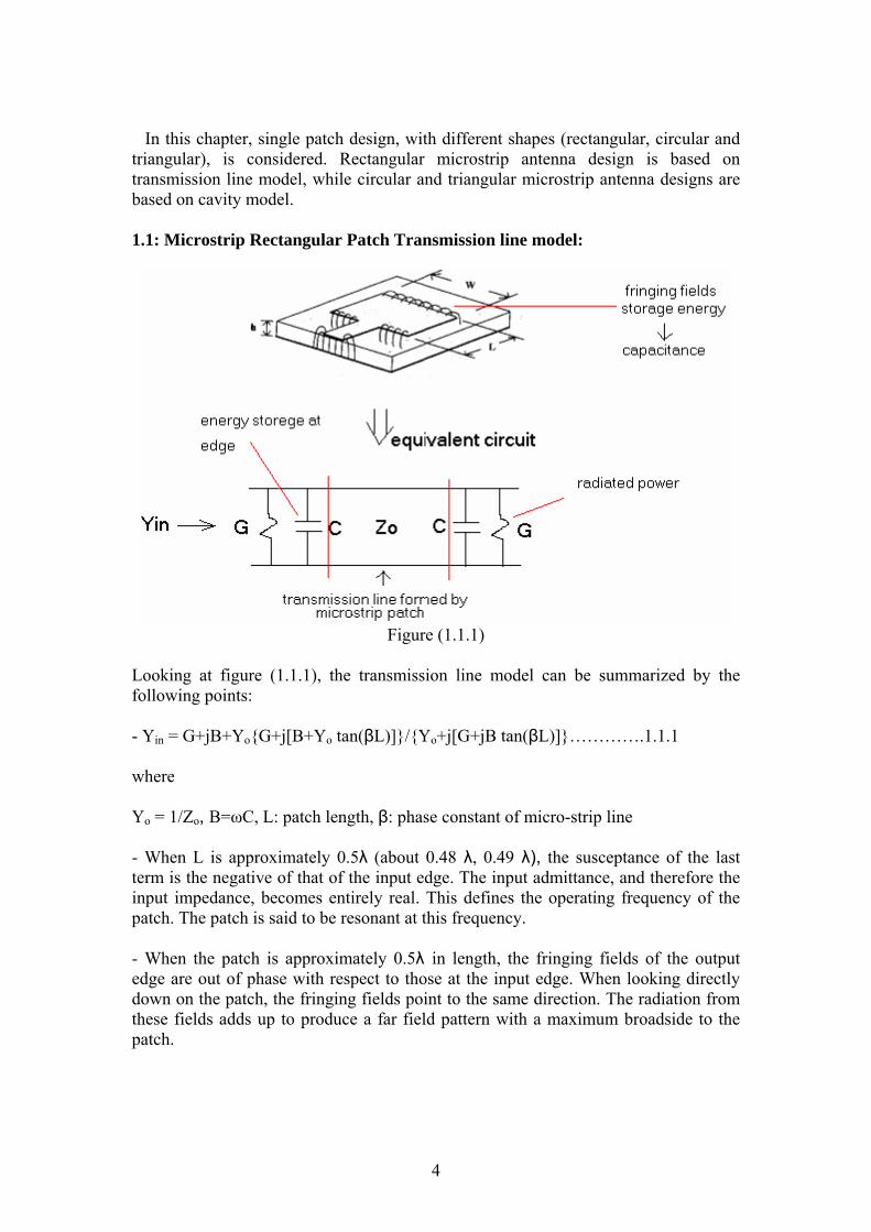
In this chapter, single patch design, with different shapes (rectangular, circular and triangular), is considered. Rectangular microstrip antenna design is based on transmission line model, while circular and triangular microstrip antenna designs are based on cavity model. 1.1: Microstrip Rectangular Patch Transmission line model:
Figure (1.1.1)
Looking at figure (1.1.1), the transmission line model can be summarized by the following points: - Yin = G+jB+YoG+j[B+Yo tan(βL)]/Yo+j[G+jB tan(βL)]………….1.1.1 where Yo = 1/Zo, B=ωC, L: patch length, β: phase constant of micro-strip line - When L is approximately 0.5λ (about 0.48 λ, 0.49 λ), the susceptance of the last term is the negative of that of the input edge. The input admittance, and therefore the input impedance, becomes entirely real. This defines the operating frequency of the patch. The patch is said to be resonant at this frequency. - When the patch is approximately 0.5λ in length, the fringing fields of the output edge are out of phase with respect to those at the input edge. When looking directly down on the patch, the fringing fields point to the same direction. The radiation from these fields adds up to produce a far field pattern with a maximum broadside to the patch.
4
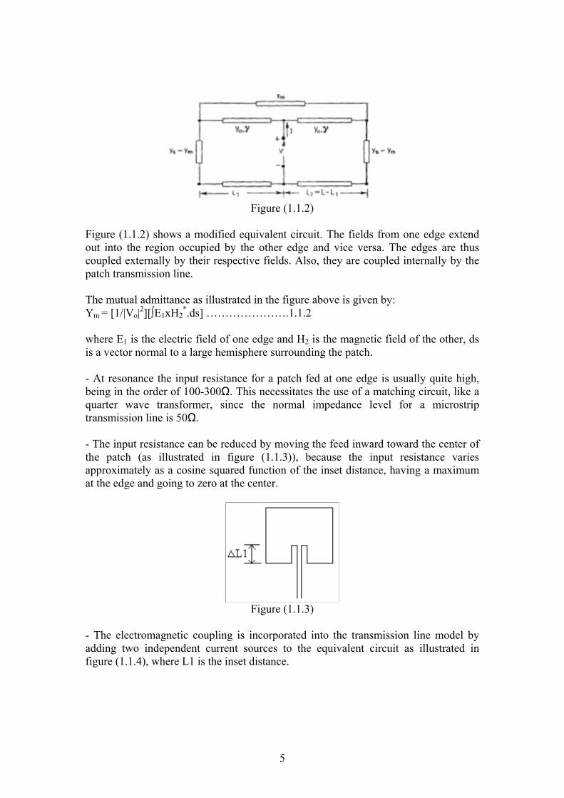
Figure (1.1.2)
Figure (1.1.2) shows a modified equivalent circuit. The fields from one edge extend out into the region occupied by the other edge and vice versa. The edges are thus coupled externally by their respective fields. Also, they are coupled internally by the patch transmission line.
The mutual admittance as illustrated in the figure above is given by: Ym = [1/|Vo|2][∫E1xH2
*.ds] ………………….1.1.2 where E1 is the electric field of one edge and H2 is the magnetic field of the other, ds is a vector normal to a large hemisphere surrounding the patch. - At resonance the input resistance for a patch fed at one edge is usually quite high, being in the order of 100-300Ω. This necessitates the use of a matching circuit, like a quarter wave transformer, since the normal impedance level for a microstrip transmission line is 50Ω. - The input resistance can be reduced by moving the feed inward toward the center of the patch (as illustrated in figure (1.1.3)), because the input resistance varies approximately as a cosine squared function of the inset distance, having a maximum at the edge and going to zero at the center.
Figure (1.1.3)
- The electromagnetic coupling is incorporated into the transmission line model by adding two independent current sources to the equivalent circuit as illustrated in figure (1.1.4), where L1 is the inset distance.
5
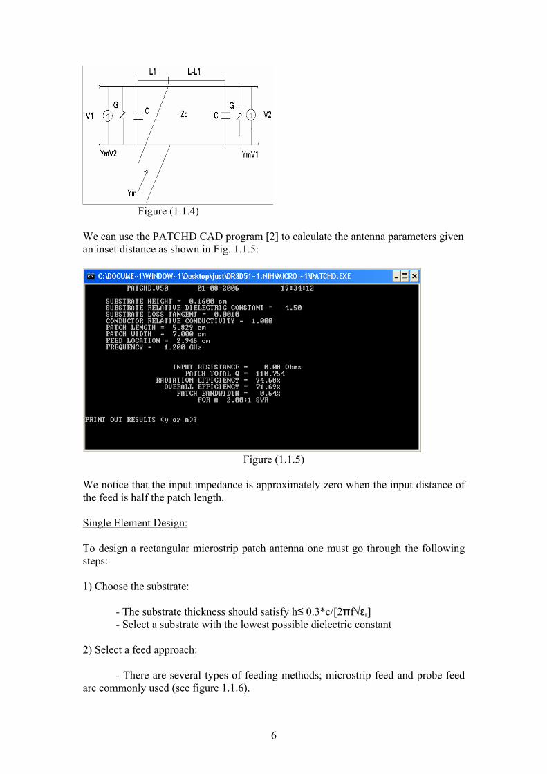
Figure (1.1.4) We can use the PATCHD CAD program [2] to calculate the antenna parameters given an inset distance as shown in Fig. 1.1.5:
Figure (1.1.5)
We notice that the input impedance is approximately zero when the input distance of the feed is half the patch length.
Single Element Design: To design a rectangular microstrip patch antenna one must go through the following steps: 1) Choose the substrate: - The substrate thickness should satisfy h≤ 0.3*c/[2πf√εr] - Select a substrate with the lowest possible dielectric constant 2) Select a feed approach: - There are several types of feeding methods; microstrip feed and probe feed are commonly used (see figure 1.1.6).
6
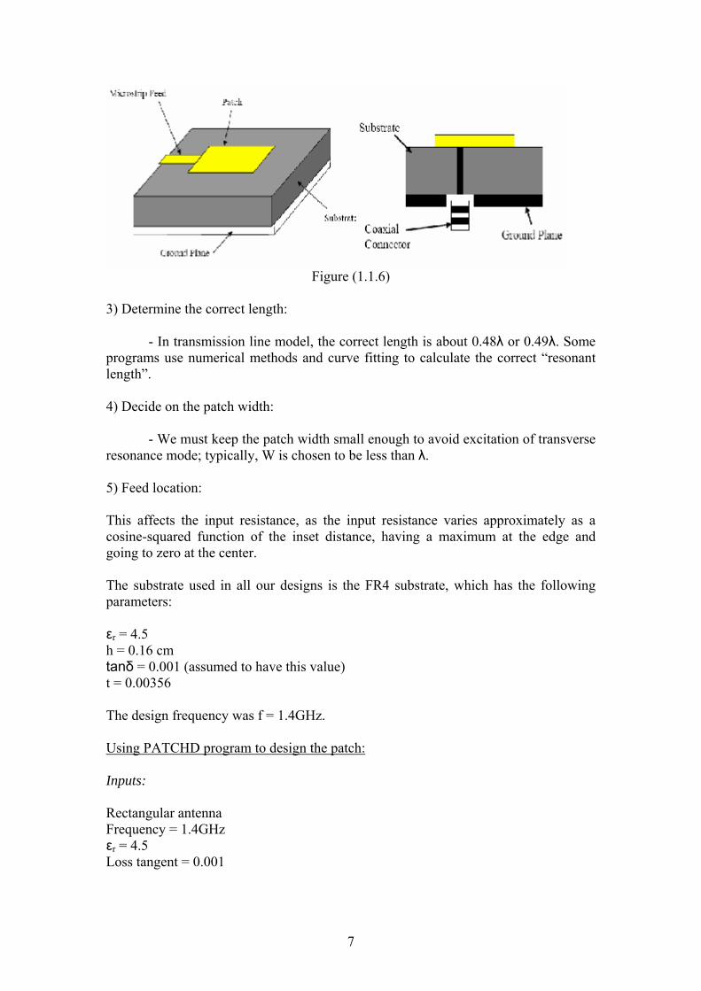
Figure (1.1.6)
3) Determine the correct length:
- In transmission line model, the correct length is about 0.48λ or 0.49λ. Some
) Decide on the patch width:
- We must keep the patch width small enough to avoid excitation of transverse
) Feed location:
his affects the input resistance, as the input resistance varies approximately as a
The substrate used in all our designs is the FR4 substrate, which has the following
r = 4.5 cm
(assumed to have this value)
he design frequency was f = 1.4GHz.
:Using PATCHD program to design the patch
programs use numerical methods and curve fitting to calculate the correct “resonant length”. 4 resonance mode; typically, W is chosen to be less than λ. 5 Tcosine-squared function of the inset distance, having a maximum at the edge and going to zero at the center.
parameters: εh = 0.16 tanδ = 0.001t = 0.00356 T
Inputs:
Rectangular antenna
gent = 0.001
Frequency = 1.4GHz εr = 4.5 Loss tan
7

The curve fitting formulas built in PATCHD are valid for 1<εr<10 which meet our choice. Patch width: To estimate the patch width; λ = c/(f √εr) = 10.10 cm Resonant length is about λ/2 = 5.05 cm We have to choose the patch width in the range 0.9<(W/L)<2 Choose W = 1.5L = 7.576 cm Substrate height = 0.16 cm We must satisfy (h/L)<0.2, also √ [(εr – 1) h]/ λo ≤ 4 Conductor conductivity relative to copper = 1 “as we use copper as a conductor in the lab”
Acceptable SWR = 2 “assumed” Feed location = 1.66 cm from the edge and we estimate the result using the phenomena that the input resistance varies as a cosine square of the input distance and we need the input resistance to be approximately 50 Ω to match the antenna with the line. Results: Patch length = 4.967 cm which is close to λ/2 as estimated Input resistance = 50.70 Ω which is close to line impedance Patch total Q = 84.345 Radiation efficiency = 93.84% Overall efficiency = 77.19% which is low
PATCH BW = 0.84% small BW Using the Autocad program, we drew the patch and printed it in the lab on the micro-strip sheet (PCB lab).
8
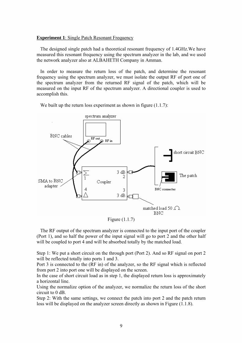
Experiment 1: Single Patch Resonant Frequency The designed single patch had a theoretical resonant frequency of 1.4GHz.We have measured this resonant frequency using the spectrum analyzer in the lab, and we used the network analyzer also at ALBAHETH Company in Amman. In order to measure the return loss of the patch, and determine the resonant frequency using the spectrum analyzer, we must isolate the output RF of port one of the spectrum analyzer from the returned RF signal of the patch, which will be measured on the input RF of the spectrum analyzer. A directional coupler is used to accomplish this. We built up the return loss experiment as shown in figure (1.1.7):
Figure (1.1.7)
The RF output of the spectrum analyzer is connected to the input port of the coupler (Port 1), and so half the power of the input signal will go to port 2 and the other half will be coupled to port 4 and will be absorbed totally by the matched load. Step 1: We put a short circuit on the through port (Port 2). And so RF signal on port 2 will be reflected totally into ports 1 and 3. Port 3 is connected to the (RF in) of the analyzer, so the RF signal which is reflected from port 2 into port one will be displayed on the screen. In the case of short circuit load as in step 1, the displayed return loss is approximately a horizontal line. Using the normalize option of the analyzer, we normalize the return loss of the short circuit to 0 dB. Step 2: With the same settings, we connect the patch into port 2 and the patch return loss will be displayed on the analyzer screen directly as shown in Figure (1.1.8).
9
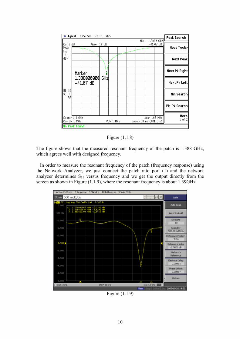
Figure (1.1.8) The figure shows that the measured resonant frequency of the patch is 1.388 GHz, which agrees well with designed frequency. In order to measure the resonant frequency of the patch (frequency response) using the Network Analyzer, we just connect the patch into port (1) and the network analyzer determines S11 versus frequency and we get the output directly from the screen as shown in Figure (1.1.9), where the resonant frequency is about 1.39GHz.
Figure (1.1.9)
10
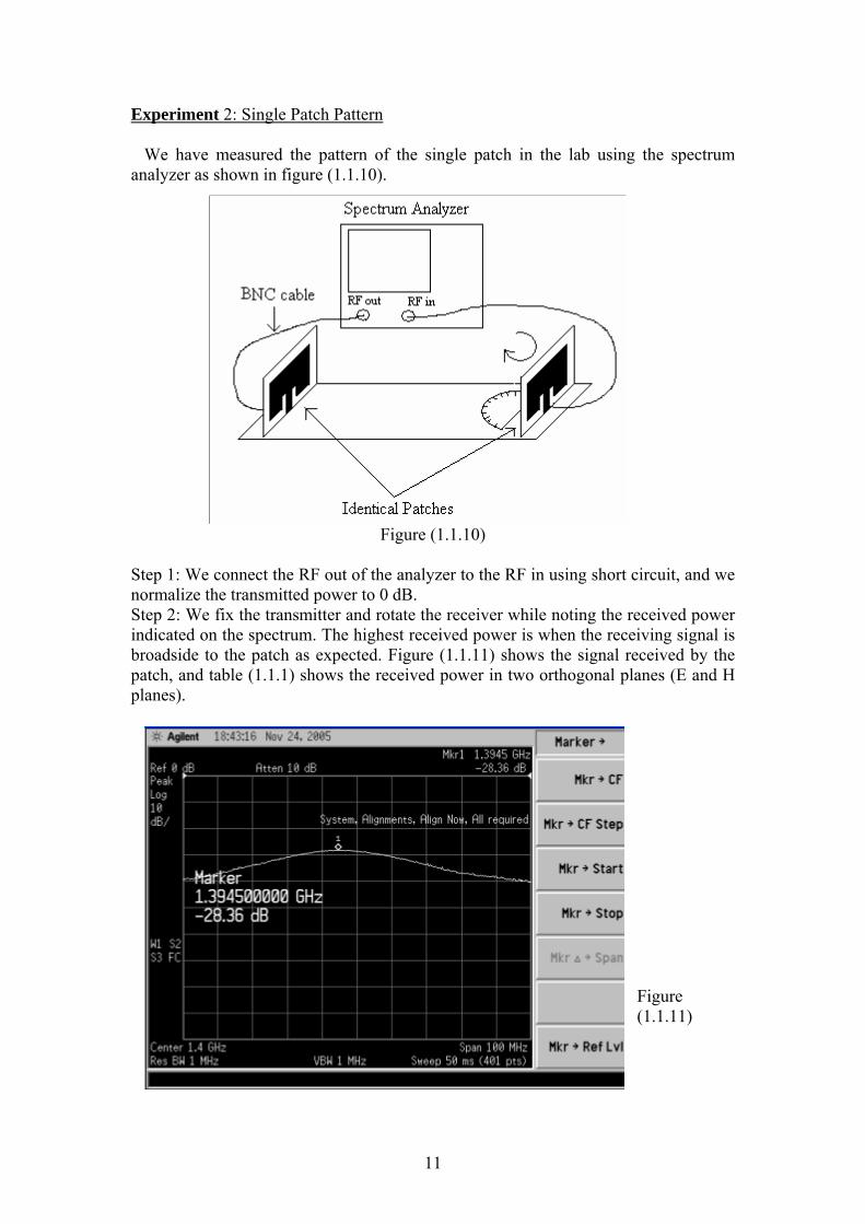
Experiment 2: Single Patch Pattern We have measured the pattern of the single patch in the lab using the spectrum analyzer as shown in figure (1.1.10).
Figure (1.1.10) Step 1: We connect the RF out of the analyzer to the RF in using short circuit, and we normalize the transmitted power to 0 dB. Step 2: We fix the transmitter and rotate the receiver while noting the received power indicated on the spectrum. The highest received power is when the receiving signal is broadside to the patch as expected. Figure (1.1.11) shows the signal received by the patch, and table (1.1.1) shows the received power in two orthogonal planes (E and H planes).
Figure (1.1.11)
11
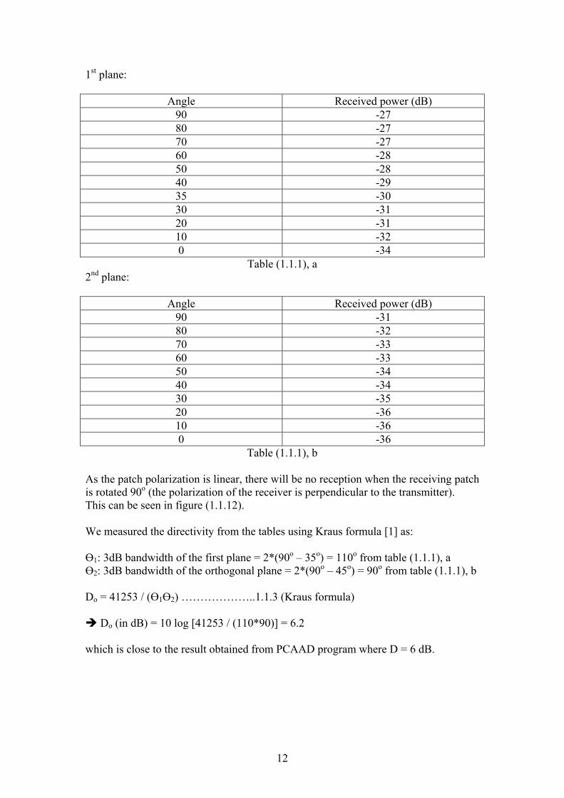
1st plane:
Angle Received power (dB) 90 -27 80 -27 70 -27 60 -28 50 -28 40 -29 35 -30 30 -31 20 -31 10 -32 0 -34
Table (1.1.1), a 2nd plane:
Angle Received power (dB) 90 -31 80 -32 70 -33 60 -33 50 -34 40 -34 30 -35 20 -36 10 -36 0 -36
Table (1.1.1), b As the patch polarization is linear, there will be no reception when the receiving patch is rotated 90o (the polarization of the receiver is perpendicular to the transmitter). This can be seen in figure (1.1.12). We measured the directivity from the tables using Kraus formula [1] as: Ө1: 3dB bandwidth of the first plane = 2*(90o – 35o) = 110o from table (1.1.1), a Ө2: 3dB bandwidth of the orthogonal plane = 2*(90o – 45o) = 90o from table (1.1.1), b Do = 41253 / (Ө1Ө2) ………………..1.1.3 (Kraus formula)
Do (in dB) = 10 log [41253 / (110*90)] = 6.2 which is close to the result obtained from PCAAD program where D = 6 dB.
12
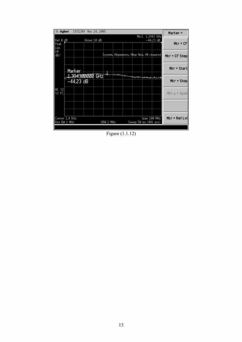
Figure (1.1.12)
13
1.2: Cavity Model: Circular Patch: A cavity is defined as closed section of waveguide and works as a resonator, and electric and magnetic energy is stored in the cavity. The electric field goes to zero at the metal walls of the cavity. Although it may not be rigorously defined for the cavity, the voltage on the wall is also zero since it is the integral of the electric field. The walls therefore act like a short circuit. A wall with an infinite conductivity is called a perfect electric conductor. It is possible to postulate a perfect magnetic conductor in which the magnetic field goes to zero. At a perfect magnetic conductor the current density and therefore the current go to zero since they are related to magnetic field the conductor acts like an open circuit. A charge distribution is established on the underside of the patch and the ground plane. At a particular instant in time, there is an accumulation of positive charges on the under side of the patch and negative charges on the ground plane. The attractive force between these charges tends to keep a large percentage of the charge between the two surfaces. The repulsive force between positive charges on the patch pushes some of these charges around the edge onto the top of the patch. For very thin substrates, the amount of charge pushed onto the top is very small. With little charge flow around the edge, it is reasonable to assume that the current goes to zero there. Perfect magnetic conductors can therefore be introduced at all four walls around the rectangular patch without greatly disturbing the field distribution. A rectangular patch can thus be viewed as a cavity resonator with perfect magnetic conductors for walls and perfect electric conductors at the top and bottom. In fact by treating the walls of the cavity as well as the material within it as lossless, the cavity would not radiate and its input impedance would be purely reactive. To account for radiation a loss mechanism has to be introduced, this can be taken into account by the radiation resistance Rr and loss resistance RL, these low resistances allow the input impedance to be complex. To make the microstrip lossy using the cavity model, which would then represent an antenna, the loss is taken into account by introducing an effective loss tangent δeff. The effective loss tangent is chosen appropriately to represent the loss mechanism of the cavity, which now behaves as an antenna and is taken as the reciprocal of the antenna quality factor Q (tan δeff = 1/Q). The modes supported by the circular patch antenna can be found by treating the patch, ground plane and the material between the two as a circular cavity. The modes that are supported by a circular microstrip antenna whose substrate height is small (h << λ) are TMz, where z is taken perpendicular to the patch. There is only one degree of freedom to control (radius of the patch) for the circular patch. Doing this does not change the order of the modes, however it does change the absolute value of the resonant frequency of each.
14
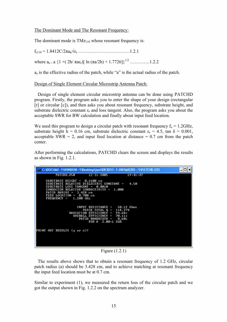
The Dominant Mode and The Resonant Frequency: The dominant mode is TMz110 whose resonant frequency is: fr110 = 1.8412C/2πae√εr …………………………….1.2.1 where ae = a 1 +( 2h/ πaεr)[ ln (πa/2h) + 1.7726]1/2 ………….1.2.2 ae is the effective radius of the patch, while “a” is the actual radius of the patch. Design of Single Element Circular Microstrip Antenna Patch: Design of single element circular microstrip antenna can be done using PATCHD program. Firstly, the program asks you to enter the shape of your design (rectangular [r] or circular [c]), and then asks you about resonant frequency, substrate height, and substrate dielectric constant εr and loss tangent. Also, the program asks you about the acceptable SWR for BW calculation and finally about input feed location. We used this program to design a circular patch with resonant frequency fo = 1.2GHz, substrate height h = 0.16 cm, substrate dielectric constant εr = 4.5, tan δ = 0.001, acceptable SWR = 2, and input feed location at distance = 0.7 cm from the patch center. After performing the calculations, PATCHD clears the screen and displays the results as shown in Fig. 1.2.1.
Figure (1.2.1)
The results above shows that to obtain a resonant frequency of 1.2 GHz, circular patch radius (a) should be 3.428 cm, and to achieve matching at resonant frequency the input feed location must be at 0.7 cm. Similar to experiment (1), we measured the return loss of the circular patch and we got the output shown in Fig. 1.2.2 on the spectrum analyzer.
15
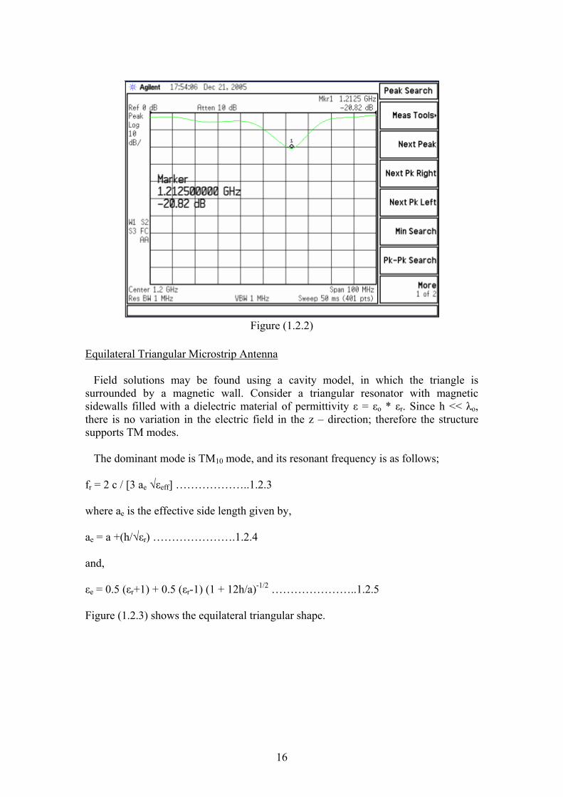
Figure (1.2.2)
Equilateral Triangular Microstrip Antenna Field solutions may be found using a cavity model, in which the triangle is surrounded by a magnetic wall. Consider a triangular resonator with magnetic sidewalls filled with a dielectric material of permittivity ε = εo * εr. Since h << λo, there is no variation in the electric field in the z – direction; therefore the structure supports TM modes. The dominant mode is TM10 mode, and its resonant frequency is as follows; fr = 2 c / [3 ae √εeff] ………………..1.2.3 where ae is the effective side length given by, ae = a +(h/√εr) ………………….1.2.4 and, εe = 0.5 (εr+1) + 0.5 (εr-1) (1 + 12h/a)-1/2 …………………..1.2.5 Figure (1.2.3) shows the equilateral triangular shape.
16

Figure (1.2.3)
The design of single element equilateral triangular microstrip antenna can be done using the above equations. From (1.2.3), ae√εe = 2c/3fr ………………………1.2.6 Substituting (1.2.4) & (1.2.5) in (1.2.6), we get the following design equation: (a + h/√εr) 0.5 (εr+1) + 0.5 (εr-1) (1 + 12h/a)-1/21/2 = 2C/3fr ……..1.2.7 We designed a single equilateral triangular patch with resonant frequency fo= 1.2GHz, substrate height h = 0.16 cm, substrate relative dielectric constant εr = 4.5. Firstly, we substitute h = 0.16 cm, εr = 4.5, C (speed of light in free space) and fr = 1.2GH in (1.2.7), also we substitute initial guess of a in (1.2.7) (this initial guess can be obtained by substituting εr instead of εe in (1.2.3) and finding ae which can be substituted in (1.2.7) as our initial guess), then by trial and error we found that for the above conditions a will be 7.94 cm. Figure (1.2.3) shows the designed triangular patch with F = 7.94 cm. Similar to experiment (1), we measured the return loss of the triangular patch and we got the output shown in Fig. 1.2.4.
Figure (1.2.4)
17

Conclusions: - We designed a rectangular microstrip antenna using PATCHD program at resonant frequency of 1.4 GHz. The measured resonant frequency obtained by the spectrum and the network analyzer was very close to the design frequency. - We designed a circular microstrip antenna using PATCHD program at resonant frequency of 1.2 GHz, the resonant frequency that we obtained by the spectrum analyzer was 1.2125 GHz. - For the triangular patch that we designed to resonate at 1.2 GHz, we got the resonant frequency at 1.2123 GHz. - The circular and triangular patch designs were based on the cavity model.
18

Chapter 2 Circularly Polarized Elements
- Truncated Patch - Nearly Squared Patch
19

Circularly Polarized Element Design
Advantages: - No need for transmitter-receiver alignment as linear polarization, and so it maximizes the received signal without consuming efforts to orient the receiver antenna. - Right and left hand circular polarization (RHCP, LHCP) are orthogonal, this can be employed to double the channel capacity on a link by having one signal use RHCP, and the other LHCP. - Reducing the effect of multi path as in mobile communication. Techniques to design CP microstrip antenna: 1) Modifying the shape of a square patch to produce an antenna that radiates CP with only one feed. 2) Using two feeds that have a specified phase and amplitude relationship to obtain CP. Single Feed CP Element: Microstrip antenna can be designed to radiate CP with no external network and only one feed. It is possible to excite the two orthogonal fields [modes] with one feed by introducing a small perturbation in the patch shape. Two types of perturbations are considered: a- Truncated (Trimmed) square single feed CP patch. b- Nearly square single feed CP patch. Truncated Patch:
Figure (2.1)
The patch is square except for the corners and it is fed at the center of one of its sides. The antenna is fed along a centerline as with a linearly polarized patch.
20
The feed excites fields under the patch just as with a linearly polarized antenna. The signal injected by the fields tends to propagate in one direction guided by the transmission line formed by the patch. In very approximate terms, the perturbation scatters the feed fields into a mode that is spatially orthogonal. Since this scattered mode sees different patch geometry, its resonant frequency is shifted slightly. To achieve CP, these two modes must be made equal in amplitude and must differ in phase by 90 deg. The equal amplitude is obtained by proper positioning of the feed. This is why the feed is placed along the patch centerline for the truncated patch. The creation of a 90-phase shift is due to two factors; one is the feed position, the other factor is the size of perturbation. Assuming a square patch lying in the (x, y) plane with its length parallel to the y- axis. For the singly fed patch one mode is excited by the feed as: Ez
1α Eo cos(kmy). The perturbation scatters some of this mode into an orthogonal mode Ez
2 α Eo cos (knx). Actually, the perturbation also modifies the original mode, creating two new modes. In the case of truncated patch the new modes are not resonant along the x and y-axes but still have orthogonal fields. The new modes have a new functional dependencies and values for kn & km. Since the perturbation is small, the changes in these quantities are expected to be small. Under these conditions, the new modes can be expressed as a linear combination of the old modes, with unknown weightings. By applying variational theory, an integral expression can be derived for the new values of k; the resonant frequencies of the modes are found. A normalization procedure is applied to the linear combination of the old modes to determine the weighting coefficients. It is possible to derive the condition for circular polarization and determine an equivalent circuit for the patch. Size of perturbation of the truncated patch; (∆S/S) = (1/2Q) …………………….2.1 where; ∆S: Area of perturbation segment S: Area of the patch Q: Antenna quality factor Let fa & fb be the new resonant frequencies; fa= fo [1-(2∆S/S)] , fb= fo ………………….2.2 where; fo is the resonant frequency of the unperturbed patch The conditions for CP occur at the arithmetic mean of the resonant frequencies. To design for a given frequency, the starting square patch should be slightly smaller than that for a corresponding LP one. At the designed frequency, the two resonant modes are dominant. Near the resonant frequencies, each mode can be modeled by a parallel RLC circuit.
21

Figure (2.2)
The resistance represents the losses associated with the mode, which are primarily due to radiation; R= Qtotal/(2πfrCo) , Co= εrεoLW/[2hcos2(πlf/L)] ……………………..2.3 lf: feed distance , h: substrate height The inductance and capacitance model the energy storage. Each mode has a transformer at its input, which represents the amount of excitation of the mode. When the CP conditions are satisfied, the turns’ ratio for each are equal (Na’ = Nb’) For all practical purposes, the mode Q’s are the same; therefore the conductance are the same. The inductance is found by setting the reactance to zero at the mode resonant frequency Li=1/(ωi
2Co) ……………2.4 where; i=a,b The turns ratio, which are equal to each other at resonance, are a function of the feed position and frequency.
Figure (2.3)
Na’ = (√S/L) | sin(kx) – sin(ky) | ...................................2.5 Nb’ = (√S/L) | sin(kx) + sin(ky) | ...................................2.6
22

where; k=π /L ..........................2.7 Nearly Squared Patch:
Figure (2.4)
L= W[1+(1/Qt)] .................2.8 Assuming that the dimensions L and W are nearly the same such that the resonant frequencies of the TMx
010 and TMx001 overlap significantly. In the broadside direction
to the patch the TMx010 mode produces an electric far field Ey;
Ey = c sin[(Π/L)y’] / [k2(1-j/Qt) - ky
2] ……………..2.9 where; c: constant , ky: Π/L , Qt = 1/tanδeff ……………..2.10 Which is linearly polarized in the y-direction While the TMx
001 mode produces an electric far field Ez Ez = c sin [(Π/W) z’]/[k2 (1-j/Qt) - kz
2] ………………………2.11 Where; c: constant, kz = Π/W, Qt = 1/tanδeff …………………….2.12 Which is linearly polarized in the z-direction. If the feed point (y’,z’) is selected along the diagonal such that; (y’/L) = (z’/W) …………………………2.13 Then the axial ratio at broadside of the Ey to the Ez field can be expressed as; (Ey/Ez) ≈ [ k(1-j/2Qt) - ky ]/[ k(1-j/2Qt) – kz ] ………………………2.14 To achieve CP; The magnitude of the axial ratio must be unity while the phase must be +90 or -90 deg. This is achieved when the two phasors representing the numerator and the denominator are of equal magnitude and 90 deg. out of phase, this can occur when; ky – kz = (k/Qt) …………………..2.15
23

and this condition is satisfied when; L= W[1+(1/Qt)] ………………………..2.16 The resonant frequencies f1 and f2 associated with two length L and W of a rectangular micro-strip: f1 = fo / √(1+(1/Qt)) , f2 = fo √(1+(1/Qt)) ……………….2.17 where; fo is the center frequency The operating frequency is selected at the mid point between the resonant frequencies of the TMx
010 and TMx001 modes.
24
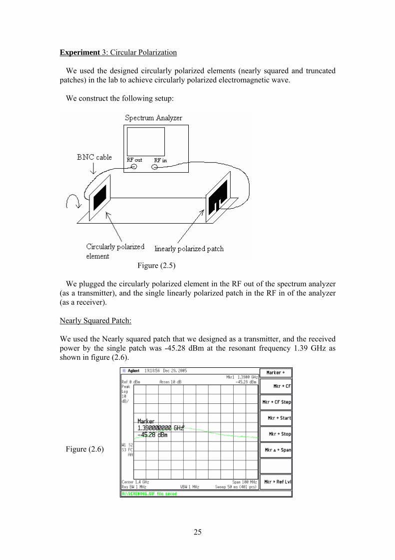
Experiment 3: Circular Polarization We used the designed circularly polarized elements (nearly squared and truncated patches) in the lab to achieve circularly polarized electromagnetic wave. We construct the following setup:
Figure (2.5) We plugged the circularly polarized element in the RF out of the spectrum analyzer (as a transmitter), and the single linearly polarized patch in the RF in of the analyzer (as a receiver). Nearly Squared Patch: We used the Nearly squared patch that we designed as a transmitter, and the received power by the single patch was -45.28 dBm at the resonant frequency 1.39 GHz as shown in figure (2.6). Figure (2.6)
25
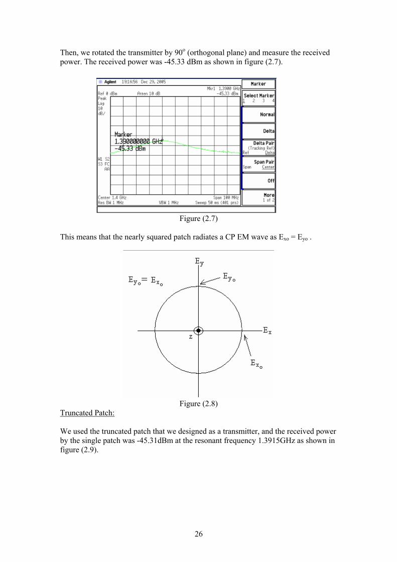
Then, we rotated the transmitter by 90o (orthogonal plane) and measure the received power. The received power was -45.33 dBm as shown in figure (2.7).
Figure (2.7) This means that the nearly squared patch radiates a CP EM wave as Exo = Eyo .
Figure (2.8)
Truncated Patch: We used the truncated patch that we designed as a transmitter, and the received power by the single patch was -45.31dBm at the resonant frequency 1.3915GHz as shown in figure (2.9).
26
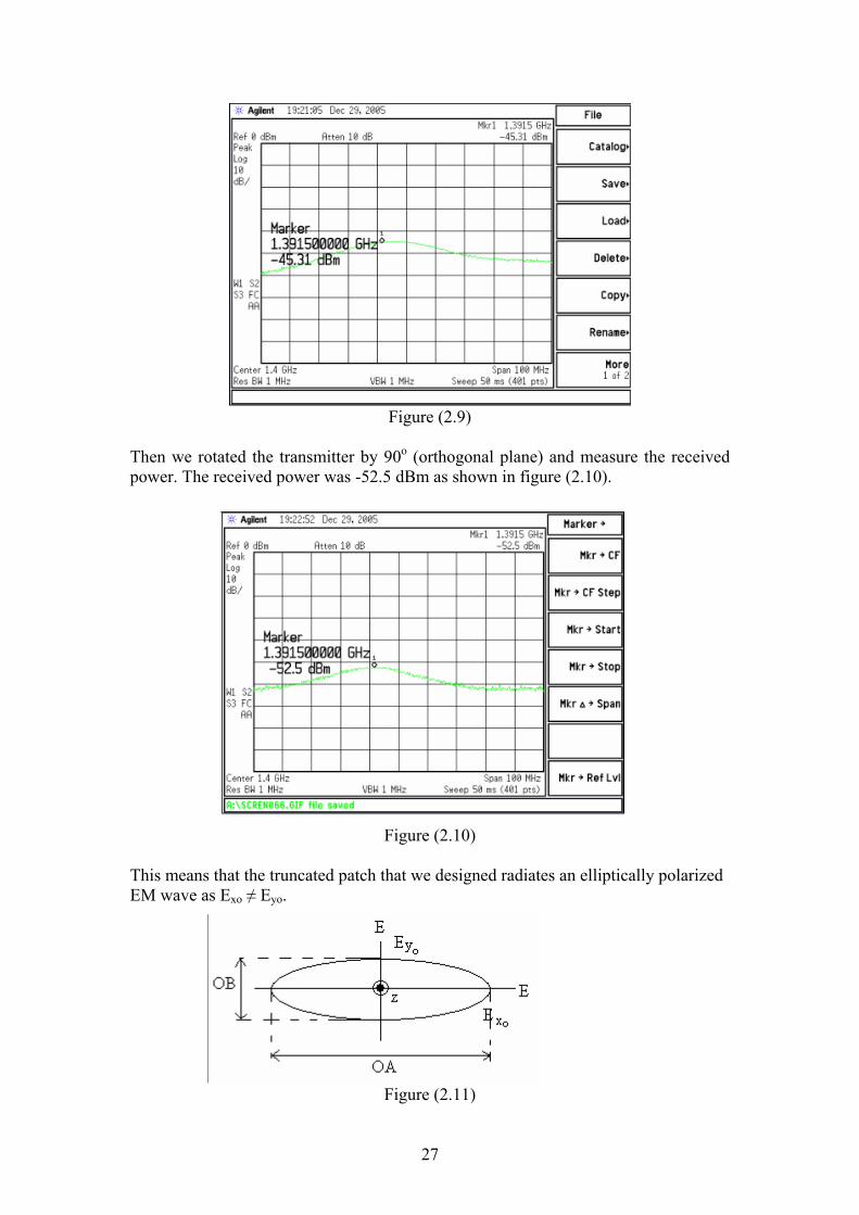
Figure (2.9)
Then we rotated the transmitter by 90o (orthogonal plane) and measure the received power. The received power was -52.5 dBm as shown in figure (2.10).
Figure (2.10)
This means that the truncated patch that we designed radiates an elliptically polarized EM wave as Exo ≠ Eyo.
Figure (2.11)
27

The axial ratio of the elliptical polarization equals (OA/OB)…………2.18 As P α E2, we can define the axial ratio; Axial ratio = √(Pr1/Pr2) ...........................2.19 Pr1/Pr2 = Pr1 (in dBm) – Pr2 (in dBm) = -45.31 – (-52.5) =7.19 dB
Pr1/Pr2 = (10) 0.719 = 5.24
axial ratio = √(5.24) = 2.288 Conclusions: - Circular polarization can be achieved by using nearly square single patch and truncated single patch microstrip antenna. - The nearly square patch that we designed and tested in the lab gave a circular polarization with axial ratio = 1. - The truncated single patch that we designed in the lab gave an elliptical polarization instead of circular, and this is due to the inadequate fabrication in the PCB lab where one of the truncated edges had a little bit different truncated edge size than the other one. This will affect the reflection of the orthogonal mode resulting in degradation in the CP radiation. - The perturbation did a small change in the resonant frequency of the patch through the scattered two resonant modes as discussed before. This can be noticed in figure (2.9). - The board’s size of the CP patch wasn’t the same as that for the single element, so there was a need to hold the CP element, which makes the patch fluctuate from the broadside, which affects the results.
28

Chapter 3 Microstrip Array
29
Microstrip Arrays
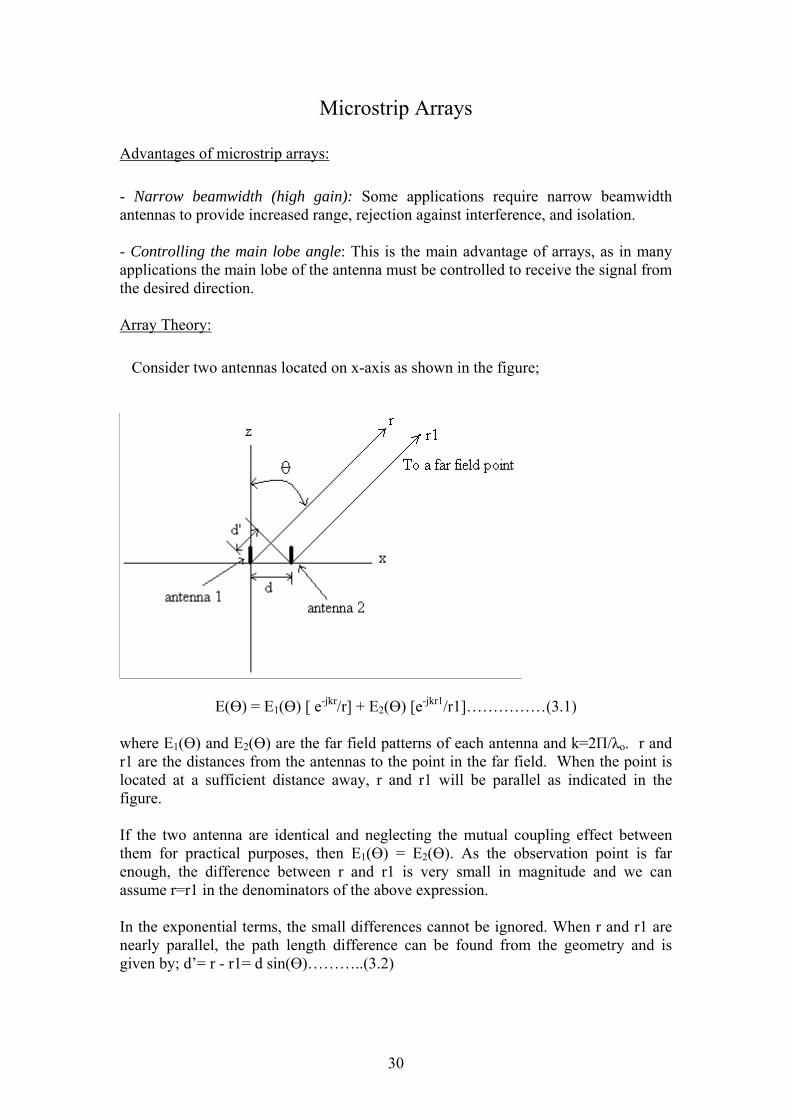
Advantages of microstrip arrays: - Narrow beamwidth (high gain): Some applications require narrow beamwidth antennas to provide increased range, rejection against interference, and isolation. - Controlling the main lobe angle: This is the main advantage of arrays, as in many applications the main lobe of the antenna must be controlled to receive the signal from the desired direction. Array Theory: Consider two antennas located on x-axis as shown in the figure;
E(Ө) = E1(Ө) [ e-jkr/r] + E2(Ө) [e-jkr1/r1]……………(3.1) where E1(Ө) and E2(Ө) are the far field patterns of each antenna and k=2Π/λo. r and r1 are the distances from the antennas to the point in the far field. When the point is located at a sufficient distance away, r and r1 will be parallel as indicated in the figure. If the two antenna are identical and neglecting the mutual coupling effect between them for practical purposes, then E1(Ө) = E2(Ө). As the observation point is far enough, the difference between r and r1 is very small in magnitude and we can assume r=r1 in the denominators of the above expression. In the exponential terms, the small differences cannot be ignored. When r and r1 are nearly parallel, the path length difference can be found from the geometry and is given by; d’= r - r1= d sin(Ө)………..(3.2)
30

The total field becomes; E(Ө) = E1(Ө) [e-jkr/r] [1+ ejkdsin(Ө)] …………………(3.3) The middle term is a consequence of the spatial spreading of the field with distance. There is no Ө variation, so this term is not of concern here. The first term is the pattern of the element and the last term is due to the array called array factor. With i and βi being the amplitude and phase of the excitation of the ith element, (3) becomes; E(Ө) = E1(Ө) [e-jkr/r] [1 + 2e-j(β2 – kd sin(Ө))]………………..(3.4) Equation (4) can be extended to cover the general case with N elements. The far field pattern is simply the sum over all elements: N E(Ө) = Ee(Ө) Σ n ej(n-1)[kd sin(Ө) – βn][e-jkr/r] ……………………..(3.5) n=1
where Ee(Ө) is the element pattern. For many cases phase shift between elements is a constant, so βn = (n-1)β. Then (5) becomes: N E(Ө) = Ee(Ө) Σ n ej(n-1)[kd sin(Ө) – β][e-jkr/r] …………………….(3.6) n=1
Let each element be excited equally in amplitude. After some algebraic manipulations, (6) reduces to:
…………………(3.7)
The pattern of any array of isotropic elements (Ee = 1 for all Ө) is plotted in figure (3.1) for arrays sizes of 3 and 12 elements. There is no phase shift between elements and the elements are spaced a half wavelength apart. These were obtained using FAZAR program for antenna arrays.
Figure (3.1)
31

There are several factors to note: 1) The beamwidth decreases with increasing array size. 2) There is one main lobe and N-2 side lobes. 3) The peak side lobe level decreases with increasing array size. An array with all elements equally excited is called a uniform array. A uniform array has the narrowest beamwidth and, consequently, the highest directivity, for a given number of elements. It also has a highest side lobe level with the peak becoming -13.2 dB as the array size gets large. The position of the main beam can be moved or steered by introducing a phase shift between elements. The maximum value of (7) occurs when kd sin (Ө) – β =0. If the main lobe is to be located at Ө = Өo , then the phase shift must be; β = kd sin (Өo) = 2Πd sin (Өo)/λo ......................................(3.8) When using a phase shift to steer the beam, the end element is set to the reference phase, say 0 deg.; the next element is phase shifted by – β; the one after by -2 β, and so on. Figure (3.2) presents pattern for a 12 elements array of half wavelength spaced isotropic elements with two different phase shifts. For purely linear phase shifts, that is equal phase shifts between adjacent elements, the pattern slides over with increasing phase shift. The larger the phase shift, the larger the beam steers. In Figure (3.2), a -20 deg. phase shift (per element) steers the beam over to about 6.4 deg., and a phase shift of -60 deg. produces a 19.5 deg. beam movement.
Figure(3.2)
For certain element spacing, multiple main beams appear in the visible space (-1< sin (Ө) <1). Figure (3.3) shows an example of this for the 12-element array. The element-to-element phase shift is -20 deg., but this time the spacing is 1.016 λo. The second beam is called a grating lobe. Usually the presence of a grating lobe is undesirable because it becomes impossible to distinguish if the signal comes from the main beam or grating lobe. For a given main beam angle, Өo, a grating lobe will not appear if the element spacing, d, does not exceed;
32
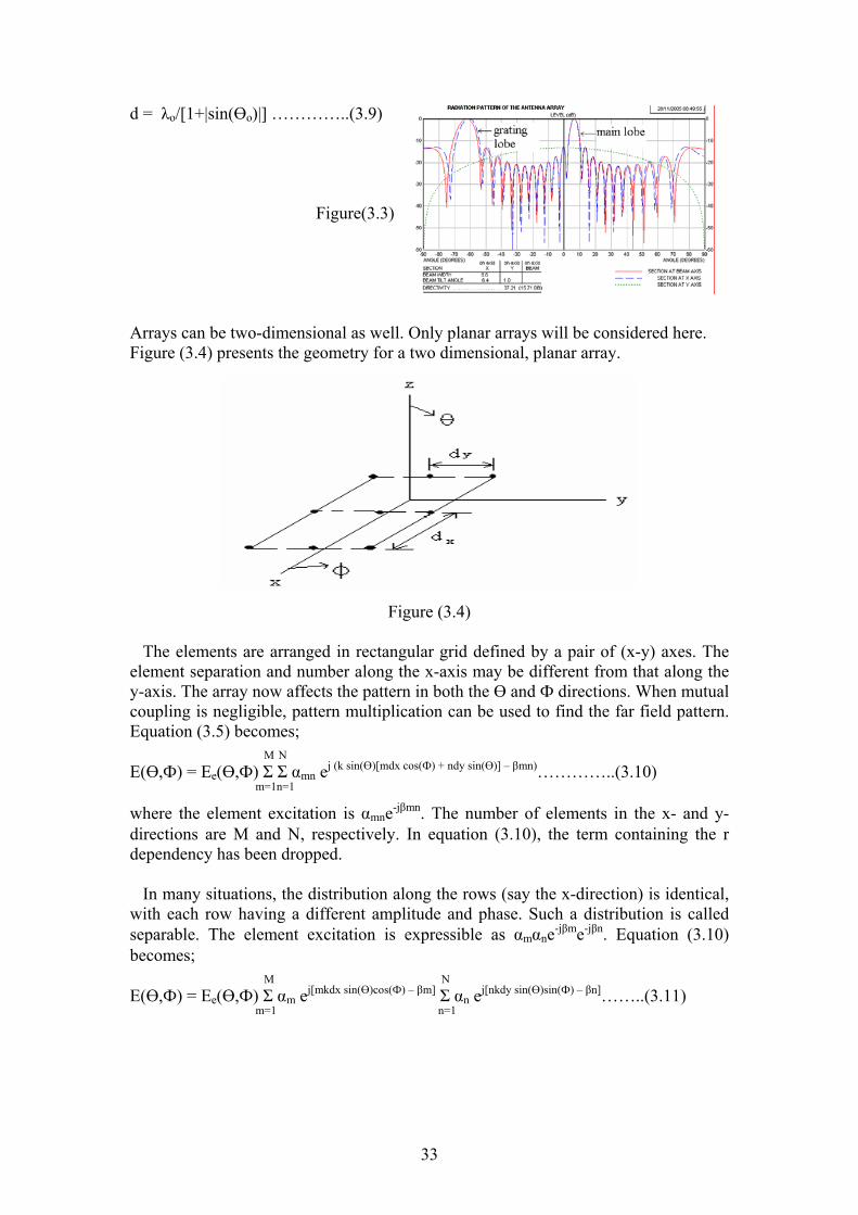
d = λo/[1+|sin(Өo)|] …………..(3.9) Figure(3.3) Arrays can be two-dimensional as well. Only planar arrays will be considered here. Figure (3.4) presents the geometry for a two dimensional, planar array.
Figure (3.4) The elements are arranged in rectangular grid defined by a pair of (x-y) axes. The element separation and number along the x-axis may be different from that along the y-axis. The array now affects the pattern in both the Ө and Ф directions. When mutual coupling is negligible, pattern multiplication can be used to find the far field pattern. Equation (3.5) becomes; M NE(Ө,Ф) = Ee(Ө,Ф) Σ Σ mn ej (k sin(Ө)[mdx cos(Ф) + ndy sin(Ө)] – βmn)…………..(3.10) m=1n=1
where the element excitation is mne-jβmn. The number of elements in the x- and y-directions are M and N, respectively. In equation (3.10), the term containing the r dependency has been dropped. In many situations, the distribution along the rows (say the x-direction) is identical, with each row having a different amplitude and phase. Such a distribution is called separable. The element excitation is expressible as mne-jβme-jβn. Equation (3.10) becomes; M N E(Ө,Ф) = Ee(Ө,Ф) Σ m ej[mkdx sin(Ө)cos(Ф) – βm] Σ n ej[nkdy sin(Ө)sin(Ф) – βn]……..(3.11) m=1 n=1
33

Finally, if the phase shifts are linear along x and y (that is, βm = (m-1)βx , βn= (n-1)βy), then; M N E(Ө,Ф) = Ee(Ө,Ф) Σ m ej(m-1)[kdx sin(Ө)cos(Ф) – βx] Σ n ej(n-1)[kdy sin(Ө)sin(Ф) – βy]………(3.12) m=1 n=1
Equation (3.12) is the product of the element pattern and two array factors (one along- x and one along- y). The advantage of the separable distribution is that it allows one to design a planar array by considering it to be two linear arrays. The phase shifts are used to steer the beam just as with a linear array. To position the main beam at Өo, Фo the required phase shifts are; βx = kdx sin(Өo)cos(Фo) ………………………………………..(3.13) βy = kdy sin(Өo)sin(Фo) ………………………………………...(3.14) Array Calculations and Analysis: We have to do quick approximations in order to design an array to meet our specifications. Several approximations have been developed on array parameters. For a linear array with a uniform excitation, the beam width is given by; Ө3dB = cos-1 [ sin(Өo) – 0.443 λo/L ] – cos-1 [ sin(Өo) + 0.443 λo/L ] ………….(3.15) where Өo is the main beam pointing angle, L is the total array length ((N-1)d), N is the number of elements and d is the element spacing. Equation (3.15) applies to scan angles from broadside to end fire arrays. The directivity of a linear array can be estimated from; D = 2L/λo = 101.5/Ө3dB ………………………………(3.16) which shows that it is directly related to the array length and inversely proportional to the beamwidth. Equation (3.16) is valid for arrays with half-wavelength spacing and uniform excitation. It is a good approximation for other spacing as well. For a planar array, it is more difficult to predict the design parameters. Assuming an array with a separable distribution, and the array is steered to the angles Өo , Фo . Let Өx be the beamwidth of a linear array having the same distribution as the planar array does in the x-direction. Similarly define Өy as the beamwidth for the distribution in the y-direction. The beamwidth in the Ф = Фo plane is; Ө-2 = cos2(Өo) [ (cos2(Фo)/ Өx
2) + (sin2(Фo)/ Өy2) ] …………………….(3.17)
In the perpendicular plane, the beamwidth is; Ф -2 = (sin2(Фo)/ Өx
2) + (cos2(Фo)/ Өy2) …………………………………(3.18)
The directivity is found from;
34

D = π DxDycos(Өo) = (32400/ӨФ) ……………………………………...(3.19) where Dx and Dy are the directivities of the equivalent linear array in the x and y-directions. Ө and Ф are given by (3.17), (3.18). Example of designing an array using ARRAYCAL program; ARRAYCAL.V10 12/01/2005 01:07:32 [Current Program Date – 01/28/96] Beamwidth and Directivity Analysis for Linear and Planar Arrays ANALYZE LINEAR (l) OR PLANAR (p) ARRAYS? l INPUT FREGUENCY (GHz)? 1.2 INPUT ELEMENT SPACING (cm)? [wavelength=25.000 (cm)] ?12.5 INPUT NUMBER OF ELEMENTS? 12 INPUT APERTURE DISRIBUTION u – UNIFORM c – COSINE-ON-A-PEDESTAL t – CHWBYSHEV ?c INPUT MAINBEAM SCALE ANGLE [broadside = 0 degrees] ?30 This program calculates the beamwidth and directivity of the array. The program output is: ARRAYCAL.V12 12/01/2005 01:07:32 LINEAR ARRAY ANALYSIS NUMBER OF ELEMENTS = 12 ELEMENT SPACING = 12.500 <cm> FREQUENCY = 1.2000 (GHz) UNIFORM DISTIBUTION MAINBEAM SCAN ANGLE = 30.00 <deg> BEAMWIDTH = 10.69 <deg> DIRECTIVITY = 9.78 (dB)
35

For a planar array design as shown in figure (3.4) using ARRAYCAL, the output of the program is as follows: ARRAYCAL.V12 12/01/2005 01:09:45 PLANER ARRAY ANALYSIS FREQUENCY = 1.2 (GHz) NUMBER OF ELEMENTS ALONG x AXIS = 12 ELEMENT SPACING = 12.500<cm> UNIFORM DISTRIBUTION NUMBER OF ELEMENTS ALONG y AXIS = 12 ELEMENT SPACING = 12.500<cm> UNIFORM DISTRIBUTION MAIN BEAM SCAN PLANE ANGLE 30.00<deg> MAIN BEAM SCAN ANGLE 60.00 <deg> SCAN PLANE BEAMWIDTH = 38.84 <deg> PERPENDICULAR PLANE BEAMWIDTH = 19.42 <deg> DIRECTIVITY = 16.33 Another program that calculates the elements excitation of a linear array and displays the pattern of the far field is APERDIST program. APERDIST can be used to adjust the distribution in order to obtain the desired sidelobe level, and determine the element excitations. There are five distributions built in the APERDIST program; 1) uniform distribution 2) linear taper on a pedestal: n = C + (1-C) [1-(2zn/L)] …………….(3.20) where n is the amplitude of the nth element, which is located at zn. The value C is the pedestal. L is the maximum location (last element).
Figure(3.5)
36

3) cosine on a pedestal: n = C + (1-C) cos[π zn/L] ……………..(3.21) 4) cosine squared on a pedestal: n = C + (1-C) cos2[π zn/L] …………….(3.22) 5) quadratic taper: n = C + (1-C) [1 – (2zn
2/L] ……….(3.23) Array Design: Figure (3.6) (in page 39) shows the 4-microstrip element planar array to be designed. The patches are identical and designed to resonate at 1.2GHz. Single Patch Design: The CAD program PATCHD was used to design the single element square patch antenna. The following parameters are entered to have the resonant frequency at 1.2 GHz and an input impedance of 50Ω. SUBSTRAIT HEIGHT = 0.1600 cm SUBSTRAIT RELATIVE DIELECTRIC CONSTANT = 4.50 SUBSTRAIT LOSS TANGENT = 0.001 CONDUCTOR RELATIVE CONDUCTIVITY = 1.000 PATCH LENGTH = 5.845 cm PATCH WIDTH = 5.845 cm FEED LOCATION = 2.235 cm FREQUENCY = 1.200 GHz The output of the program was as follows: INPUT RESISTANCE = 50.46 Ohms PATCH TOTAL Q = 124.044 RADIATION EFFICIENCY = 94.68% OVERALL EFFICIENCY = 68.94% PATCH BANDWIDTH = 0.57% For A 2.00:1 SWR Feed Line Design: The array is fed from the bottom using a 50Ω coaxial line. The inner conductor of the coax is soldered to the 100Ω microstrip line, and the outer conductor is connected to the ground plane. Since the coax is feeding two 100Ω microstrip lines in parallel, no mismatch occurs at this input as the parallel combination of the two microstrip line is equal to 50Ω. The microstrip lines (50Ω and 100Ω) are designed using the program TLINE, the following data is obtained: Ro = 50Ω ---------------------- W = 3.06 mm, εeff = 3.4534
Ro = 100Ω --------------------- W = 0.698 mm, εeff = 3.1244
37

where W is the microstrip width and; εeff = (λo / λg)2 ………………(3.24) is the effective permittivity of the microstrip line from which λg can be obtained Ro = 50Ω ----------------------- λg = 13.45 cm Ro = 100Ω ----------------------- λg = 14.14 cm The input feed lines for the patches are chosen to be 50Ω lines with feed points at 2.235 cm from the radiating edge. Thus, no mismatch exists at the input of the patches. To match the 100Ω line to the 25Ω equivalent resistance of the parallel two 50Ω lines, a quarter wavelength transformer is used. The transformer line should have Ro = √(100*25) = 50Ω …………………(3.25) The length of the transformer is λg/4 = 3.36 cm ………………….(3.26) Main beam direction: For the array of figure (3.6), the main beam is directed broadside to the array if there were no input phase difference from element to element. To direct the main beam at some other angle, the element should be fed with different phases to make a uniform array. In our design, unequal line lengths will be used to produce phase shifts, which yield fixed beams that are scanned away from broadside. The phase shift in y–direction (βy) can be varied by varying the location of the feed point along the 100-Ω line. While, (βx) will be fixed through the different length of the patches feeders. We design the main beam to be fixed at Өo = 30o in the E-plane. Thus βx should satisfy; βx = -2π (dx/λ) sin(Өo) ………………..(3.27) βx = - π (dx/λ) In order to avoid grating lobes, we should choose; (dx/λ) < 1/(1+|sin(Өo)|) = 0.67 ……………..(3.28) In our design, we have chosen (dx/λ) = 0.4 ………………..(3.29) Which gives dx = 10 cm Thus, line lengths (in the x-direction) should be chosen to create a phase shift; βx = -1.257 rad. ……………………….(3.30)
38
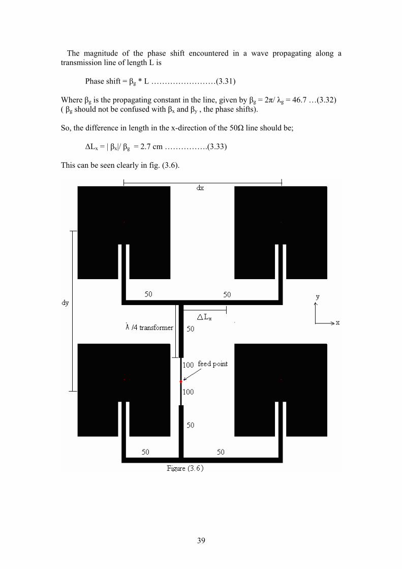
The magnitude of the phase shift encountered in a wave propagating along a transmission line of length L is Phase shift = βg * L ……………………(3.31) Where βg is the propagating constant in the line, given by βg = 2π/ λg = 46.7 …(3.32) ( βg should not be confused with βx and βy , the phase shifts). So, the difference in length in the x-direction of the 50Ω line should be; ∆Lx = | βx|/ βg = 2.7 cm …………….(3.33) This can be seen clearly in fig. (3.6).
39
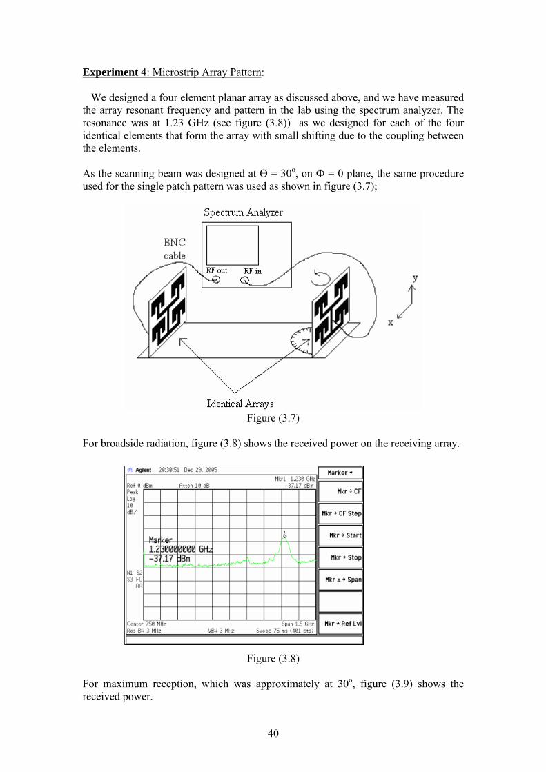
Experiment 4: Microstrip Array Pattern: We designed a four element planar array as discussed above, and we have measured the array resonant frequency and pattern in the lab using the spectrum analyzer. The resonance was at 1.23 GHz (see figure (3.8)) as we designed for each of the four identical elements that form the array with small shifting due to the coupling between the elements. As the scanning beam was designed at Ө = 30o, on Ф = 0 plane, the same procedure used for the single patch pattern was used as shown in figure (3.7);
Figure (3.7)
For broadside radiation, figure (3.8) shows the received power on the receiving array.
Figure (3.8) For maximum reception, which was approximately at 30o, figure (3.9) shows the received power.
40
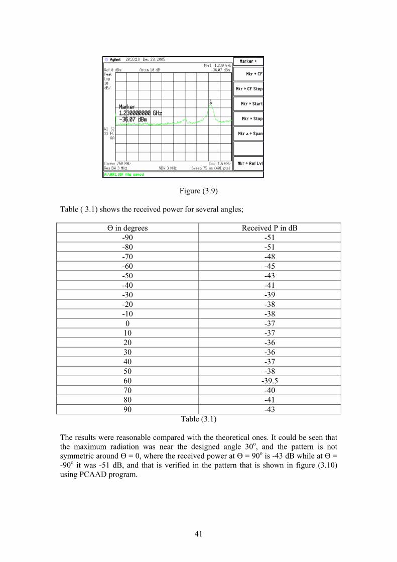
Figure (3.9) Table ( 3.1) shows the received power for several angles;
Ө in degrees Received P in dB -90 -51 -80 -51 -70 -48 -60 -45 -50 -43 -40 -41 -30 -39 -20 -38 -10 -38 0 -37 10 -37 20 -36 30 -36 40 -37 50 -38 60 -39.5 70 -40 80 -41 90 -43
Table (3.1) The results were reasonable compared with the theoretical ones. It could be seen that the maximum radiation was near the designed angle 30o, and the pattern is not symmetric around Ө = 0, where the received power at Ө = 90o is -43 dB while at Ө = -90o it was -51 dB, and that is verified in the pattern that is shown in figure (3.10) using PCAAD program.
41
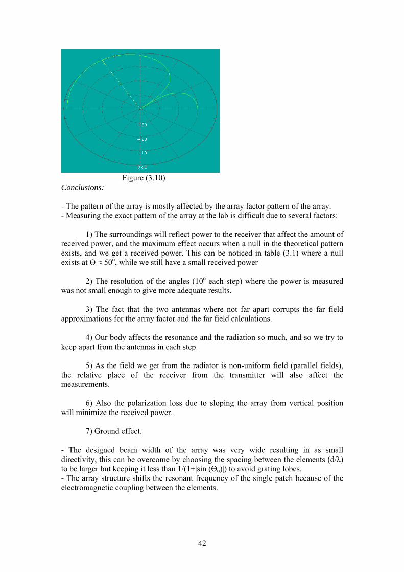
Figure (3.10) Conclusions: - The pattern of the array is mostly affected by the array factor pattern of the array. - Measuring the exact pattern of the array at the lab is difficult due to several factors:
1) The surroundings will reflect power to the receiver that affect the amount of
received power, and the maximum effect occurs when a null in the theoretical pattern exists, and we get a received power. This can be noticed in table (3.1) where a null exists at Ө ≈ 50o, while we still have a small received power 2) The resolution of the angles (10o each step) where the power is measured was not small enough to give more adequate results. 3) The fact that the two antennas where not far apart corrupts the far field approximations for the array factor and the far field calculations. 4) Our body affects the resonance and the radiation so much, and so we try to keep apart from the antennas in each step. 5) As the field we get from the radiator is non-uniform field (parallel fields), the relative place of the receiver from the transmitter will also affect the measurements. 6) Also the polarization loss due to sloping the array from vertical position will minimize the received power.
7) Ground effect. - The designed beam width of the array was very wide resulting in as small directivity, this can be overcome by choosing the spacing between the elements (d/λ) to be larger but keeping it less than 1/(1+|sin (Өo)|) to avoid grating lobes. - The array structure shifts the resonant frequency of the single patch because of the electromagnetic coupling between the elements.
42

Chapter 4 Broadband Elements
43
Broad Bandwidth Elements
Introduction: The major limitation of microstrip antenna is narrow bandwidth. Almost always, the factor that limits the bandwidth is the impedance behavior of the antenna. Much effort has gone into broadening the impedance bandwidth. Some has involved attempting to realize the broadband through better matching techniques. In our project we use other approach that broadens the bandwidth by using multiple elements that are parasitically coupled to the original patch. Before we start to study this approach we have to study the bandwidth limitations of microstrip antenna. Microstrip Antenna Bandwidth Limitations: The relatively rapid change in impedance with frequency is the major factor determining the patch bandwidth. Patches are resonant structures that look like a parallel RLC circuits in and around the resonant frequency. Like any resonant circuit, the impedance behavior with frequency is closely linked to the patch quality factor Q. Typical Q's are around 60 to 70. Patches are one of many types of low gain antennas and it can be shown that for low gain antennas, the antenna Q is inversely proportional to the volume occupied by the antenna as measured in terms of wavelengths (this is derived from Maxwell's equations). Since the bandwidth is determined by the patch physical size, one way to increase bandwidth is to increase the antenna size. This approach is followed in bandwidth enhancement techniques that use multiple elements. For a single element, making the antenna longer, wider, or thicker can increase the size of the patch. The patch length is fixed by requirement to be resonant. Only lowering the substrate dielectric constant, which is usually desirable because of reduced surface-wave excitation, can lengthen it. Increasing the patch width is possible as long as it remains less than a wavelength in the dielectric; since beyond a wavelength width, higher order modes may be exited that create pattern distortions and unpredictable impedance behavior. Perhaps the easiest way to increase the patch bandwidth is by using a thick substrate (i.e. increase h as long as h < .05λ0) this limitation on h is to keep the surface-wave excitation on its minimum value.
44
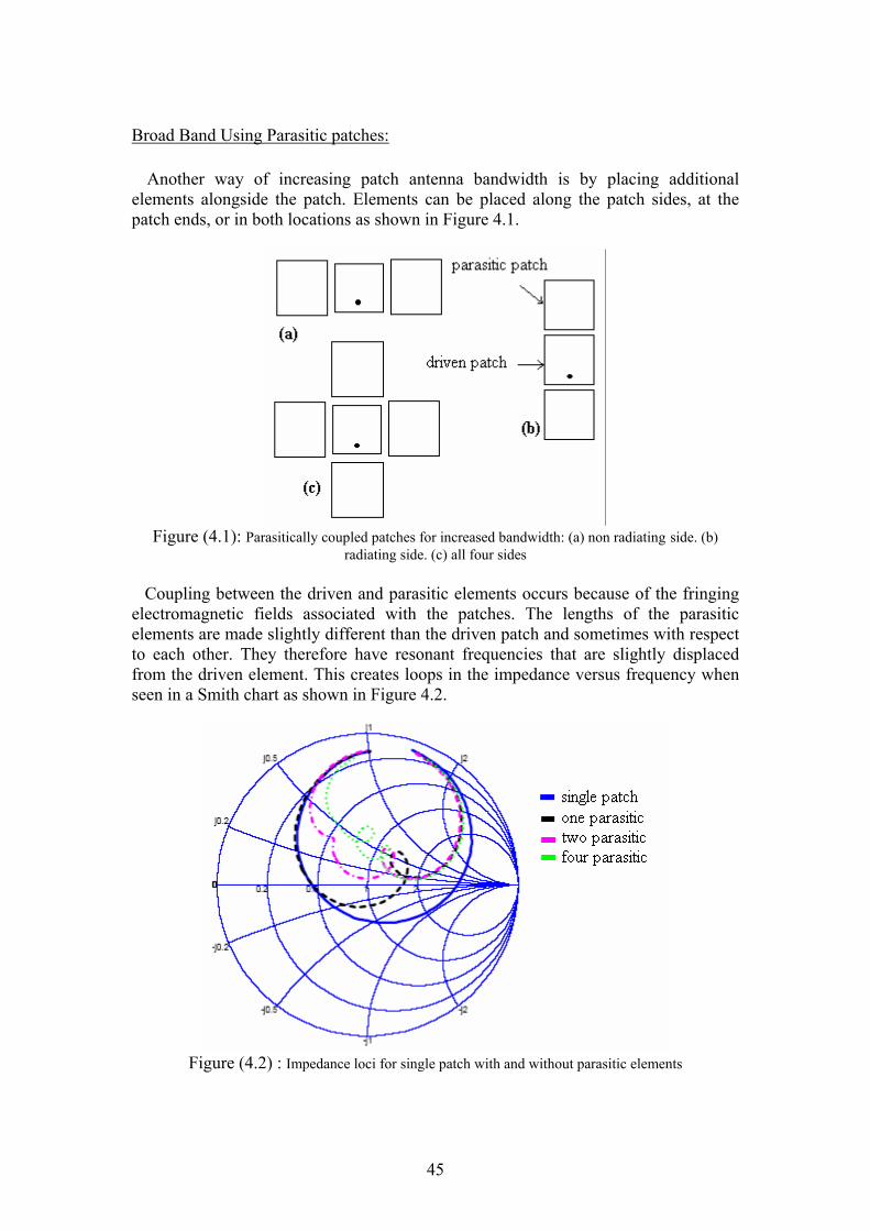
Broad Band Using Parasitic patches: Another way of increasing patch antenna bandwidth is by placing additional elements alongside the patch. Elements can be placed along the patch sides, at the patch ends, or in both locations as shown in Figure 4.1.
Figure (4.1): Parasitically coupled patches for increased bandwidth: (a) non radiating side. (b)
radiating side. (c) all four sides Coupling between the driven and parasitic elements occurs because of the fringing electromagnetic fields associated with the patches. The lengths of the parasitic elements are made slightly different than the driven patch and sometimes with respect to each other. They therefore have resonant frequencies that are slightly displaced from the driven element. This creates loops in the impedance versus frequency when seen in a Smith chart as shown in Figure 4.2.
Figure (4.2) : Impedance loci for single patch with and without parasitic elements
45
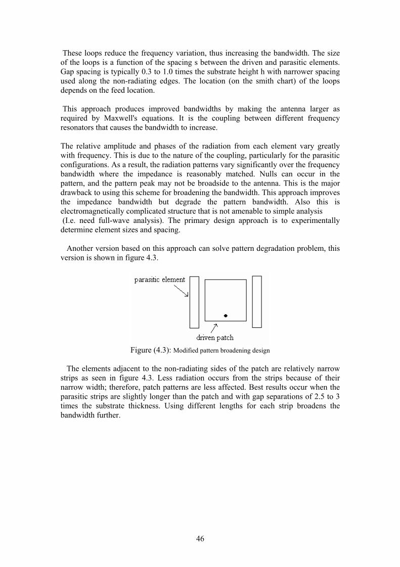
These loops reduce the frequency variation, thus increasing the bandwidth. The size of the loops is a function of the spacing s between the driven and parasitic elements. Gap spacing is typically 0.3 to 1.0 times the substrate height h with narrower spacing used along the non-radiating edges. The location (on the smith chart) of the loops depends on the feed location. This approach produces improved bandwidths by making the antenna larger as required by Maxwell's equations. It is the coupling between different frequency resonators that causes the bandwidth to increase. The relative amplitude and phases of the radiation from each element vary greatly with frequency. This is due to the nature of the coupling, particularly for the parasitic configurations. As a result, the radiation patterns vary significantly over the frequency bandwidth where the impedance is reasonably matched. Nulls can occur in the pattern, and the pattern peak may not be broadside to the antenna. This is the major drawback to using this scheme for broadening the bandwidth. This approach improves the impedance bandwidth but degrade the pattern bandwidth. Also this is electromagnetically complicated structure that is not amenable to simple analysis (I.e. need full-wave analysis). The primary design approach is to experimentally determine element sizes and spacing. Another version based on this approach can solve pattern degradation problem, this version is shown in figure 4.3.
Figure (4.3): Modified pattern broadening design
The elements adjacent to the non-radiating sides of the patch are relatively narrow strips as seen in figure 4.3. Less radiation occurs from the strips because of their narrow width; therefore, patch patterns are less affected. Best results occur when the parasitic strips are slightly longer than the patch and with gap separations of 2.5 to 3 times the substrate thickness. Using different lengths for each strip broadens the bandwidth further.
46

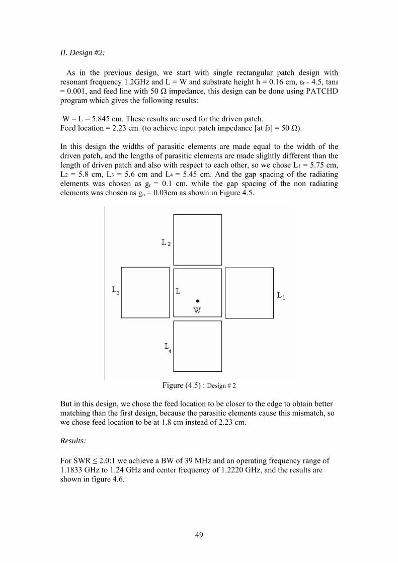
Design of Broadband Rectangular and Triangular Microstrip Antenna Using Parasitic Elements: I. Design #1: Firstly, we started with single rectangular patch design with resonant frequency 1.2GHz and L = W and substrate height h = 0.16 cm, εr = 4.5, tanδ = 0.001, and feed line with 50 Ω impedance, this design can be done using PATCHD program which gives the following results: W = L = 5.845 cm. Feed location = 2.23 cm. (to achieve input patch impedance [at f0] = 50 Ω). In this design the widths and lengths of parasitic elements are made equal to the width and length of the driven patch, and the gap spacing of the radiating elements gr = 0.1 cm, while the gap spacing of the non radiating elements gn = 0.03cm as shown in Figure 4.4.
Figure (4.4): Design # 1
Results: For SWR ≤ 2.0:1 we achieve a BW of 29 MH and an operating frequency range of 1.2060 GHz to 1.2348 GHz and center frequency of 1.2215 GHz, and the results are shown in figure 4.5.
47
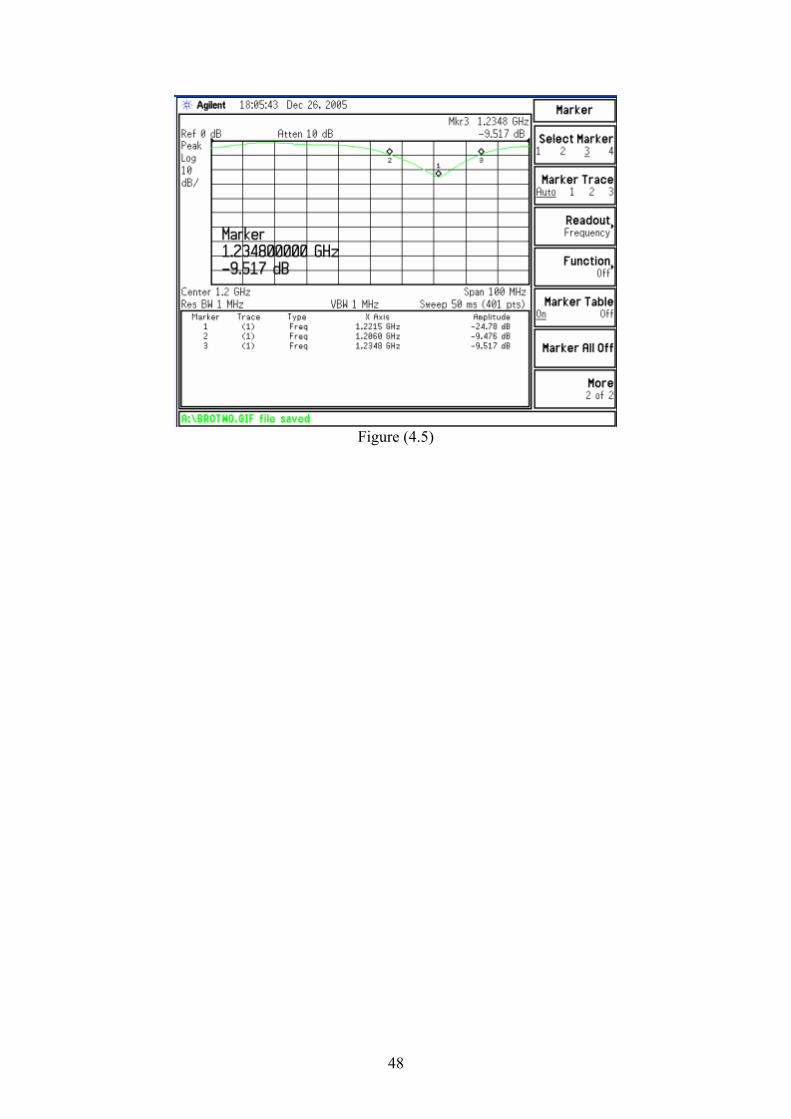
Figure (4.5)
48
II. Design #2: As in the previous design, we start with single rectangular patch design with resonant frequency 1.2GHz and L = W and substrate height h = 0.16 cm, εr = 4.5, tanδ = 0.001, and feed line with 50 Ω impedance, this design can be done using PATCHD program which gives the following results: W = L = 5.845 cm. These results are used for the driven patch. Feed location = 2.23 cm. (to achieve input patch impedance [at f0] = 50 Ω). In this design the widths of parasitic elements are made equal to the width of the driven patch, and the lengths of parasitic elements are made slightly different than the length of driven patch and also with respect to each other, so we chose L1 = 5.75 cm, L2 = 5.8 cm, L3 = 5.6 cm and L4 = 5.45 cm. And the gap spacing of the radiating elements was chosen as gr = 0.1 cm, while the gap spacing of the non radiating elements was chosen as gn = 0.03cm as shown in Figure 4.5.
Figure (4.5) : Design # 2
But in this design, we chose the feed location to be closer to the edge to obtain better matching than the first design, because the parasitic elements cause this mismatch, so we chose feed location to be at 1.8 cm instead of 2.23 cm. Results: For SWR ≤ 2.0:1 we achieve a BW of 39 MHz and an operating frequency range of 1.1833 GHz to 1.24 GHz and center frequency of 1.2220 GHz, and the results are shown in figure 4.6.
49
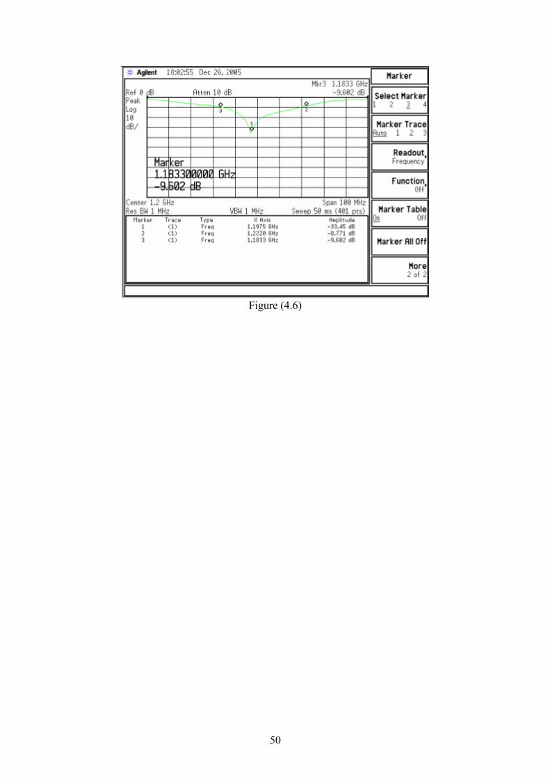
Figure (4.6)
50

III. Design # 3: In this design, we used only two parasitic elements adjacent to the non-radiating sides of the patch, and they are relatively narrow strips. This design provides a compromise between the BW improvement and pattern degradation where the patch patterns are less affected. As in previous designs, we also start with single rectangular patch design with resonant frequency 1.2GHZ and L = W and substrate height h = 0.16 cm, εr = 4.5, tanδ = 0.001, and feed line with 50 Ω impedance, this design can be done using PATCHD program which gives us this results: W = L = 5.845 cm. These results are used for the driven patch. Feed location = 2.23 cm. (to achieve input patch impedance [at f0] = 50 Ω). In this design the parasitic elements widths were chosen to be narrow, so they were chosen to be W1 = W2 = 1.2 cm, also we chose the parasitic lengths to be slightly longer than the patch length, so we chose L1 = 6 cm and L2 = 6.15 cm. And the gap spacing was chosen as g = 0.46 cm as shown in Figure 4.7
Figure (4.7): Design # 3
But in this design we chose the feed location to be closer to the edge to obtain better matching than the first design, because the parasitic elements cause this mismatch, so we chose feed location to be at 2 cm instead of 2.23 cm. Results: For SWR ≤ 2.0:1 we achieve a BW of 36 MHz and an operating frequency range of 1.1853 GHz to 1.2208 GHz and center frequency of 1.1978 GHz, and the results are shown in figure 4.8.
51
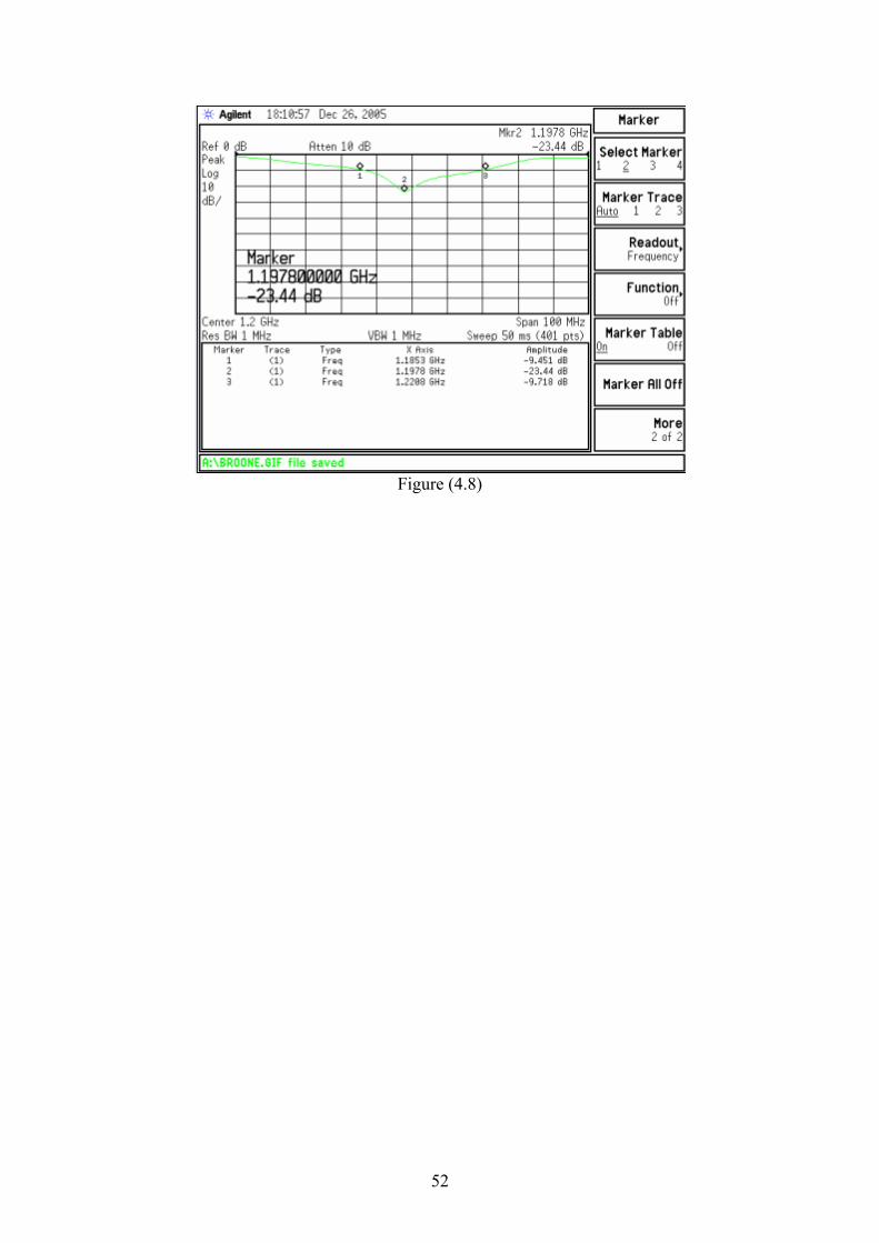
Figure (4.8)
52

IV. Design # 4: Equilateral triangular patches were chosen as second option because their performance is similar to the rectangular patch but occupy less space. The method that was used to design the rectangular antenna was used to design triangular antenna; first, a single narrowband triangular antenna was designed. The specifications for this antenna were the same as those of the rectangular design. Once the narrowband design was completed a broadband design was made using parasitic patch elements. We start with single equilateral triangular patch design with resonant frequency 1.2GHz and substrate height h = 0.16 cm, εr = 4.5, tanδ = 0.001, and feed line with 50 Ω impedance, Figure 4.9 shows a general design for an equilateral triangular patch antenna,
Figure (4.9)
where a can be determined using the following equations: fr = 2C / 3ae√εe …………………..4.1 εe = 0.5 (εr+1) + 0.5 (εr-1) (1 + 12h/a)-1/2 ………………….4.2 ae = a + h/√εr ………………………..4.3 Using above equations we found a = 7.94 cm. Now we can use the same approach used during construction of the rectangular antenna, but in triangular antenna two parasitic elements were added instead of four elements in rectangular design case, and this is because that the rectangular design required four elements - one placed by each of the patch edges - to achieve an acceptable result, while the triangular design only utilizes two parasitic elements to achieve a good broadband result, Figure 4.10 shows the broadband triangular design.
53
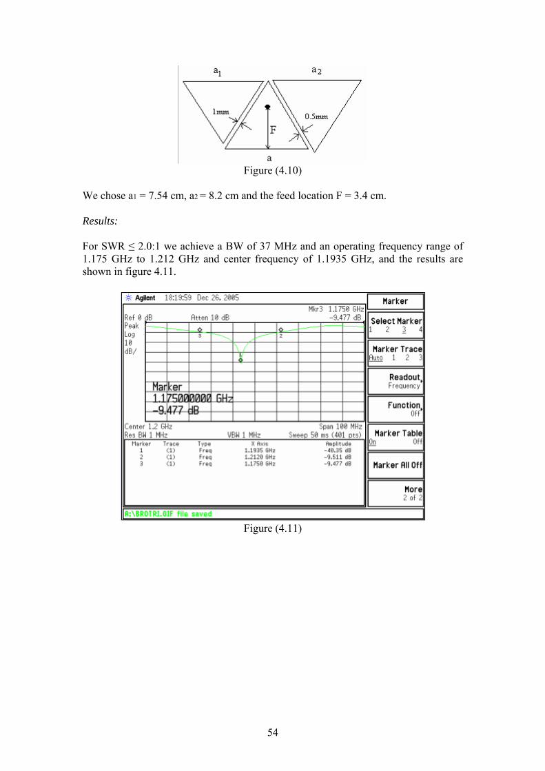
Figure (4.10)
We chose a1 = 7.54 cm, a2 = 8.2 cm and the feed location F = 3.4 cm. Results: For SWR ≤ 2.0:1 we achieve a BW of 37 MHz and an operating frequency range of 1.175 GHz to 1.212 GHz and center frequency of 1.1935 GHz, and the results are shown in figure 4.11.
Figure (4.11)
54

Conclusions: - The major limitation of microstrip antennas is narrow bandwidth. - The relatively rapid change in impedance with frequency is the major factor determining the patch bandwidth. - There are many approaches to broaden the bandwidth of microstrip antenna. In our project, we used parasitic elements for this aim. - The parasitic elements increase the size occupied by the antenna. This increases the bandwidth (this is derived from Maxwell’s equations). - In our project we did four designs to broaden the bandwidth, three designs are based on rectangular patch, and the fourth one is based on equilateral triangular patch, and these four designs are based on parasitic elements approach. - In our case the primary design approach is to experimentally determine element size and spacing. - In design # 1 we start with five identical patches and inset feed location as for single patch. For SWR ≤ 2:1 we got bandwidth of 29 MHz, and center frequency of 1.2215 GHz, where the return loss at the center frequency was equal 24.78 dB. - In design # 2, we modified design #1 by making the length of the parasitic patches slightly different than the driven patch and with respect to each other , this allows more bandwidth broadening and -as expected- we got bandwidth of 39 MHz (mor bandwidth than design #1) for SWR ≤ 2:1. - In design # 2 another modification was added. We moved the inset feed location slightly towards the patch edge to obtain better matching than the first one, and as expected the return loss at the center frequency (fo = 1.222 GHz) was equal 33.45 dB, while the return loss of the design # 1 at the center frequency was equal 24.78 dB. As a disadvantage of this design nulls can occur in the pattern, and the pattern peak may not be broadside to the antenna. - In design # 3 we used only two narrow strips parasitic elements adjacent to the non-radiating patch sides. This design provides a compromise between bandwidth improvement and pattern degradation, and as expected we obtained bandwidth of 36 MHz that is less than design # 2 bandwidth for SWR ≤ 2:1. - In design # 4 we used a triangular patch instead of rectangular patch to preserve more space and we got for SWR ≤ 2:1 bandwidth of 37 MHz. - The addition of parasitic elements shifts the resonant frequency of the single patch because of the EM coupling between the elements.
55

References [1] C. A. Balanis, Antenna Theory: Analysis and Design, second edition [2] R. A. Sainati, CAD of Microstrip Antennas for Wireless Applications, 1996 [3] I. J. Bahl, P. Bhartia, Microstrip Antennas, second edition [4] J. R. James, P. S. Hall, Hand Book of Microstrip Antennas, [5] D. M.Pozar, Microwave Engineering, second edition [6] Internet Resources
56
Appendix1
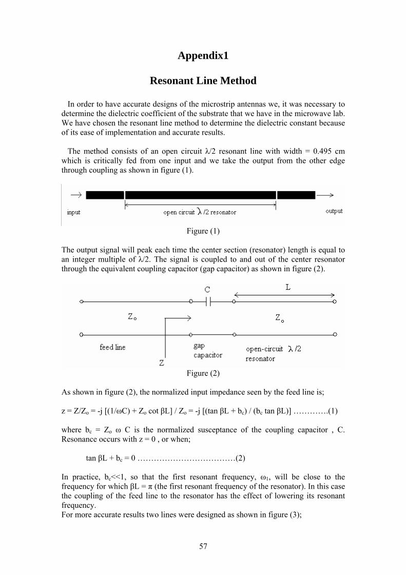
Resonant Line Method In order to have accurate designs of the microstrip antennas we, it was necessary to determine the dielectric coefficient of the substrate that we have in the microwave lab. We have chosen the resonant line method to determine the dielectric constant because of its ease of implementation and accurate results. The method consists of an open circuit λ/2 resonant line with width = 0.495 cm which is critically fed from one input and we take the output from the other edge through coupling as shown in figure (1).
Figure (1)
The output signal will peak each time the center section (resonator) length is equal to an integer multiple of λ/2. The signal is coupled to and out of the center resonator through the equivalent coupling capacitor (gap capacitor) as shown in figure (2).
Figure (2)
As shown in figure (2), the normalized input impedance seen by the feed line is; z = Z/Zo = -j [(1/ωC) + Zo cot βL] / Zo = -j [(tan βL + bc) / (bc tan βL)] ………….(1) where bc = Zo ω C is the normalized susceptance of the coupling capacitor , C. Resonance occurs with z = 0 , or when; tan βL + bc = 0 ………………………………(2) In practice, bc<<1, so that the first resonant frequency, ω1, will be close to the frequency for which βL = π (the first resonant frequency of the resonator). In this case the coupling of the feed line to the resonator has the effect of lowering its resonant frequency. For more accurate results two lines were designed as shown in figure (3);
57

Figure (3)
…………………………….. (3) Where f1 and f2 are the resonant frequencies of the two lengths, n1 and n2 are the orders of resonance for the two lengths. l1 and l2 are the lengths of the resonance sections, and c is the speed of light.
…………………..(4)
58
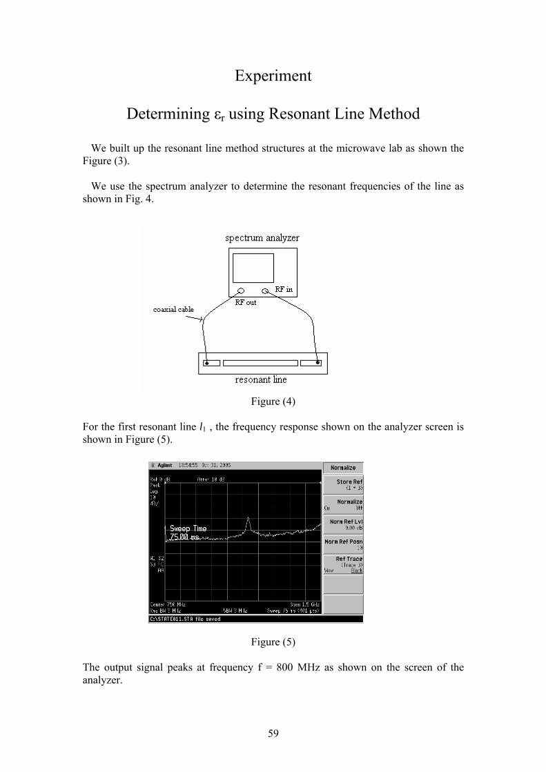
Experiment
Determining εr using Resonant Line Method We built up the resonant line method structures at the microwave lab as shown the Figure (3). We use the spectrum analyzer to determine the resonant frequencies of the line as shown in Fig. 4.
Figure (4)
For the first resonant line l1 , the frequency response shown on the analyzer screen is shown in Figure (5).
Figure (5) The output signal peaks at frequency f = 800 MHz as shown on the screen of the analyzer.
59
Knowing that l1 = 10 cm = λ/2; we get λ = 20 cm λ = c /(f *√εeff) √εeff = c / (λ*f) εeff = [c / (λ*f)]2 = [3*108 / (0.2*800*106)]2 =3.5 using,
Where h = 0.16 cm (substrate height), W = 0.495 cm (line width) 3.5 = (εr +1)/2 + [(εr – 1)/2][1+12*0.16/0.495]-0.5
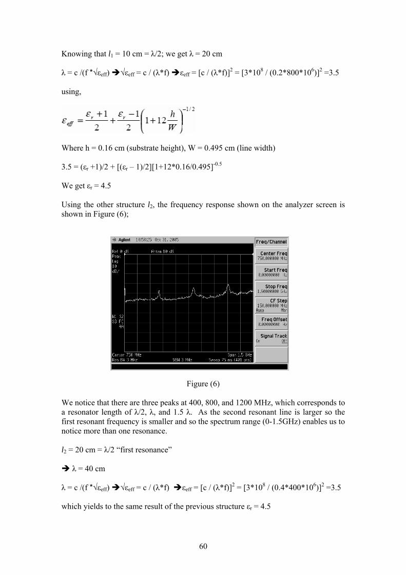
We get εr = 4.5 Using the other structure l2, the frequency response shown on the analyzer screen is shown in Figure (6);
Figure (6) We notice that there are three peaks at 400, 800, and 1200 MHz, which corresponds to a resonator length of λ/2, λ, and 1.5 λ. As the second resonant line is larger so the first resonant frequency is smaller and so the spectrum range (0-1.5GHz) enables us to notice more than one resonance. l2 = 20 cm = λ/2 “first resonance”
λ = 40 cm λ = c /(f *√εeff) √εeff = c / (λ*f) εeff = [c / (λ*f)]2 = [3*108 / (0.4*400*106)]2 =3.5 which yields to the same result of the previous structure εr = 4.5
60

Using,
we will get the same answer; εeff = [3*108*(1*800*106 –2*800*106)] / [2*800*106*400*106*(0.4-0.2)]2 = 3.5 and so εr = 4.5
61

Appendix 2
A picture of the designed microstrip structures
62