pci express to pci bus translation bridge (rev. b · 2011-04-23 · xio2000 pci express to pci bus...
TRANSCRIPT

XIO2000 PCI Express to PCI BusTranslation Bridge
Data Manual
Literature Number: SCPS097BNovember 2005
Printed on Recycled Paper

IMPORTANT NOTICE
Texas Instruments Incorporated and its subsidiaries (TI) reserve the right to make corrections, modifications,enhancements, improvements, and other changes to its products and services at any time and to discontinueany product or service without notice. Customers should obtain the latest relevant information before placingorders and should verify that such information is current and complete. All products are sold subject to TI’s termsand conditions of sale supplied at the time of order acknowledgment.
TI warrants performance of its hardware products to the specifications applicable at the time of sale inaccordance with TI’s standard warranty. Testing and other quality control techniques are used to the extent TIdeems necessary to support this warranty. Except where mandated by government requirements, testing of allparameters of each product is not necessarily performed.
TI assumes no liability for applications assistance or customer product design. Customers are responsible fortheir products and applications using TI components. To minimize the risks associated with customer productsand applications, customers should provide adequate design and operating safeguards.
TI does not warrant or represent that any license, either express or implied, is granted under any TI patent right,copyright, mask work right, or other TI intellectual property right relating to any combination, machine, or processin which TI products or services are used. Information published by TI regarding third-party products or servicesdoes not constitute a license from TI to use such products or services or a warranty or endorsement thereof.Use of such information may require a license from a third party under the patents or other intellectual propertyof the third party, or a license from TI under the patents or other intellectual property of TI.
Reproduction of information in TI data books or data sheets is permissible only if reproduction is withoutalteration and is accompanied by all associated warranties, conditions, limitations, and notices. Reproductionof this information with alteration is an unfair and deceptive business practice. TI is not responsible or liable forsuch altered documentation.
Resale of TI products or services with statements different from or beyond the parameters stated by TI for thatproduct or service voids all express and any implied warranties for the associated TI product or service andis an unfair and deceptive business practice. TI is not responsible or liable for any such statements.
Following are URLs where you can obtain information on other Texas Instruments products and applicationsolutions:
Products Applications
Amplifiers amplifier.ti.com Audio www.ti.com/audio
Data Converters dataconverter.ti.com Automotive www.ti.com/automotive
DSP dsp.ti.com Broadband www.ti.com/broadband
Interface interface.ti.com Digital Control www.ti.com/digitalcontrol
Logic logic.ti.com Military www.ti.com/military
Power Mgmt power.ti.com Optical Networking www.ti.com/opticalnetwork
Microcontrollers microcontroller.ti.com Security www.ti.com/security
Telephony www.ti.com/telephony
Video & Imaging www.ti.com/video
Wireless www.ti.com/wireless
Mailing Address: Texas Instruments
Post Office Box 655303 Dallas, Texas 75265
Copyright 2005, Texas Instruments Incorporated
iiiNovember 2005 SCPS097B
ContentsSection Page
1 XIO2000 Features 1 . . . . . . . . . . . . . . . . . . . . . . . . . . . . . . . . . . . . . . . . . . . . . . . . . . . . . . . . . . . . . . . . . . . . . . . 2 Introduction 2 . . . . . . . . . . . . . . . . . . . . . . . . . . . . . . . . . . . . . . . . . . . . . . . . . . . . . . . . . . . . . . . . . . . . . . . . . . . .
2.1 Description 2 . . . . . . . . . . . . . . . . . . . . . . . . . . . . . . . . . . . . . . . . . . . . . . . . . . . . . . . . . . . . . . . . . . . . . . 2.2 Related Documents 2 . . . . . . . . . . . . . . . . . . . . . . . . . . . . . . . . . . . . . . . . . . . . . . . . . . . . . . . . . . . . . . . 2.3 Trademarks 2 . . . . . . . . . . . . . . . . . . . . . . . . . . . . . . . . . . . . . . . . . . . . . . . . . . . . . . . . . . . . . . . . . . . . . . 2.4 Document Conventions 3 . . . . . . . . . . . . . . . . . . . . . . . . . . . . . . . . . . . . . . . . . . . . . . . . . . . . . . . . . . . . 2.5 Document History 3 . . . . . . . . . . . . . . . . . . . . . . . . . . . . . . . . . . . . . . . . . . . . . . . . . . . . . . . . . . . . . . . . . 2.6 Ordering Information 3 . . . . . . . . . . . . . . . . . . . . . . . . . . . . . . . . . . . . . . . . . . . . . . . . . . . . . . . . . . . . . . 2.7 Terminal Assignments 4 . . . . . . . . . . . . . . . . . . . . . . . . . . . . . . . . . . . . . . . . . . . . . . . . . . . . . . . . . . . . . 2.8 Terminal Descriptions 8 . . . . . . . . . . . . . . . . . . . . . . . . . . . . . . . . . . . . . . . . . . . . . . . . . . . . . . . . . . . . .
3 Feature/Protocol Descriptions 15 . . . . . . . . . . . . . . . . . . . . . . . . . . . . . . . . . . . . . . . . . . . . . . . . . . . . . . . . . . . 3.1 Power-Up/-Down Sequencing 15 . . . . . . . . . . . . . . . . . . . . . . . . . . . . . . . . . . . . . . . . . . . . . . . . . . . . . .
3.1.1 Power-Up Sequence 15 . . . . . . . . . . . . . . . . . . . . . . . . . . . . . . . . . . . . . . . . . . . . . . . . . . . . . 3.1.2 Power-Down Sequence 16 . . . . . . . . . . . . . . . . . . . . . . . . . . . . . . . . . . . . . . . . . . . . . . . . . .
3.2 Bridge Reset Features 17 . . . . . . . . . . . . . . . . . . . . . . . . . . . . . . . . . . . . . . . . . . . . . . . . . . . . . . . . . . . . 3.3 PCI Express Interface 18 . . . . . . . . . . . . . . . . . . . . . . . . . . . . . . . . . . . . . . . . . . . . . . . . . . . . . . . . . . . . .
3.3.1 External Reference Clock 18 . . . . . . . . . . . . . . . . . . . . . . . . . . . . . . . . . . . . . . . . . . . . . . . . 3.3.2 Beacon 19 . . . . . . . . . . . . . . . . . . . . . . . . . . . . . . . . . . . . . . . . . . . . . . . . . . . . . . . . . . . . . . . . 3.3.3 Wake 19 . . . . . . . . . . . . . . . . . . . . . . . . . . . . . . . . . . . . . . . . . . . . . . . . . . . . . . . . . . . . . . . . . . 3.3.4 Initial Flow Control Credits 19 . . . . . . . . . . . . . . . . . . . . . . . . . . . . . . . . . . . . . . . . . . . . . . . . 3.3.5 PCI Express Message Transactions 19 . . . . . . . . . . . . . . . . . . . . . . . . . . . . . . . . . . . . . . .
3.4 PCI Bus Interface 20 . . . . . . . . . . . . . . . . . . . . . . . . . . . . . . . . . . . . . . . . . . . . . . . . . . . . . . . . . . . . . . . . . 3.4.1 I/O Characteristics 20 . . . . . . . . . . . . . . . . . . . . . . . . . . . . . . . . . . . . . . . . . . . . . . . . . . . . . . 3.4.2 Clamping Voltage 20 . . . . . . . . . . . . . . . . . . . . . . . . . . . . . . . . . . . . . . . . . . . . . . . . . . . . . . . 3.4.3 PCI Bus Clock Run 21 . . . . . . . . . . . . . . . . . . . . . . . . . . . . . . . . . . . . . . . . . . . . . . . . . . . . . . 3.4.4 PCI Bus External Arbiter 21 . . . . . . . . . . . . . . . . . . . . . . . . . . . . . . . . . . . . . . . . . . . . . . . . . 3.4.5 MSI Messages Generated from the Serial IRQ Interface 22 . . . . . . . . . . . . . . . . . . . . . . 3.4.6 PCI Bus Clocks 23 . . . . . . . . . . . . . . . . . . . . . . . . . . . . . . . . . . . . . . . . . . . . . . . . . . . . . . . . .
3.5 Quality of Service and Isochronous Features 23 . . . . . . . . . . . . . . . . . . . . . . . . . . . . . . . . . . . . . . . . . 3.5.1 PCI Port Arbitration 24 . . . . . . . . . . . . . . . . . . . . . . . . . . . . . . . . . . . . . . . . . . . . . . . . . . . . . . 3.5.2 PCI Isochronous Windows 25 . . . . . . . . . . . . . . . . . . . . . . . . . . . . . . . . . . . . . . . . . . . . . . . . 3.5.3 PCI Express Extended VC With VC Arbitration 26 . . . . . . . . . . . . . . . . . . . . . . . . . . . . . . 3.5.4 128-Phase, WRR PCI Port Arbitration Timing 27 . . . . . . . . . . . . . . . . . . . . . . . . . . . . . . .
3.6 Configuration Register Translation 28 . . . . . . . . . . . . . . . . . . . . . . . . . . . . . . . . . . . . . . . . . . . . . . . . . . 3.7 PCI Interrupt Conversion to PCI Express Messages 29 . . . . . . . . . . . . . . . . . . . . . . . . . . . . . . . . . . . 3.8 PME Conversion to PCI Express Messages 30 . . . . . . . . . . . . . . . . . . . . . . . . . . . . . . . . . . . . . . . . . . 3.9 PCI Express To PCI Bus Lock Conversion 31 . . . . . . . . . . . . . . . . . . . . . . . . . . . . . . . . . . . . . . . . . . . 3.10 Two-Wire Serial-Bus Interface 32 . . . . . . . . . . . . . . . . . . . . . . . . . . . . . . . . . . . . . . . . . . . . . . . . . . . . . .
3.10.1 Serial-Bus Interface Implementation 33 . . . . . . . . . . . . . . . . . . . . . . . . . . . . . . . . . . . . . . . 3.10.2 Serial-Bus Interface Protocol 33 . . . . . . . . . . . . . . . . . . . . . . . . . . . . . . . . . . . . . . . . . . . . . . 3.10.3 Serial-Bus EEPROM Application 35 . . . . . . . . . . . . . . . . . . . . . . . . . . . . . . . . . . . . . . . . . . 3.10.4 Accessing Serial-Bus Devices Through Software 37 . . . . . . . . . . . . . . . . . . . . . . . . . . . .
3.11 Advanced Error Reporting Registers 37 . . . . . . . . . . . . . . . . . . . . . . . . . . . . . . . . . . . . . . . . . . . . . . . . 3.12 Data Error Forwarding Capability 37 . . . . . . . . . . . . . . . . . . . . . . . . . . . . . . . . . . . . . . . . . . . . . . . . . . . 3.13 General-Purpose I/O Interface 38 . . . . . . . . . . . . . . . . . . . . . . . . . . . . . . . . . . . . . . . . . . . . . . . . . . . . . . 3.14 Set Slot Power Limit Functionality 38 . . . . . . . . . . . . . . . . . . . . . . . . . . . . . . . . . . . . . . . . . . . . . . . . . . . 3.15 PCI Express and PCI Bus Power Management 38 . . . . . . . . . . . . . . . . . . . . . . . . . . . . . . . . . . . . . . .

Contents
iv November 2005SCPS097B
Section Page
4 Classic PCI Configuration Space 40 . . . . . . . . . . . . . . . . . . . . . . . . . . . . . . . . . . . . . . . . . . . . . . . . . . . . . . . . 4.1 Vendor ID Register 41 . . . . . . . . . . . . . . . . . . . . . . . . . . . . . . . . . . . . . . . . . . . . . . . . . . . . . . . . . . . . . . . . 4.2 Device ID Register 41 . . . . . . . . . . . . . . . . . . . . . . . . . . . . . . . . . . . . . . . . . . . . . . . . . . . . . . . . . . . . . . . . 4.3 Command Register 42 . . . . . . . . . . . . . . . . . . . . . . . . . . . . . . . . . . . . . . . . . . . . . . . . . . . . . . . . . . . . . . . 4.4 Status Register 43 . . . . . . . . . . . . . . . . . . . . . . . . . . . . . . . . . . . . . . . . . . . . . . . . . . . . . . . . . . . . . . . . . . . 4.5 Class Code and Revision ID Register 44 . . . . . . . . . . . . . . . . . . . . . . . . . . . . . . . . . . . . . . . . . . . . . . . . 4.6 Cache Line Size Register 44 . . . . . . . . . . . . . . . . . . . . . . . . . . . . . . . . . . . . . . . . . . . . . . . . . . . . . . . . . . 4.7 Primary Latency Timer Register 44 . . . . . . . . . . . . . . . . . . . . . . . . . . . . . . . . . . . . . . . . . . . . . . . . . . . . 4.8 Header Type Register 44 . . . . . . . . . . . . . . . . . . . . . . . . . . . . . . . . . . . . . . . . . . . . . . . . . . . . . . . . . . . . . 4.9 BIST Register 45 . . . . . . . . . . . . . . . . . . . . . . . . . . . . . . . . . . . . . . . . . . . . . . . . . . . . . . . . . . . . . . . . . . . . 4.10 Device Control Base Address Register 45 . . . . . . . . . . . . . . . . . . . . . . . . . . . . . . . . . . . . . . . . . . . . . . 4.11 Primary Bus Number Register 45 . . . . . . . . . . . . . . . . . . . . . . . . . . . . . . . . . . . . . . . . . . . . . . . . . . . . . . 4.12 Secondary Bus Number Register 46 . . . . . . . . . . . . . . . . . . . . . . . . . . . . . . . . . . . . . . . . . . . . . . . . . . . 4.13 Subordinate Bus Number Register 46 . . . . . . . . . . . . . . . . . . . . . . . . . . . . . . . . . . . . . . . . . . . . . . . . . . 4.14 Secondary Latency Timer Register 46 . . . . . . . . . . . . . . . . . . . . . . . . . . . . . . . . . . . . . . . . . . . . . . . . . . 4.15 I/O Base Register 46 . . . . . . . . . . . . . . . . . . . . . . . . . . . . . . . . . . . . . . . . . . . . . . . . . . . . . . . . . . . . . . . . . 4.16 I/O Limit Register 47 . . . . . . . . . . . . . . . . . . . . . . . . . . . . . . . . . . . . . . . . . . . . . . . . . . . . . . . . . . . . . . . . . 4.17 Secondary Status Register 48 . . . . . . . . . . . . . . . . . . . . . . . . . . . . . . . . . . . . . . . . . . . . . . . . . . . . . . . . . 4.18 Memory Base Register 49 . . . . . . . . . . . . . . . . . . . . . . . . . . . . . . . . . . . . . . . . . . . . . . . . . . . . . . . . . . . . 4.19 Memory Limit Register 49 . . . . . . . . . . . . . . . . . . . . . . . . . . . . . . . . . . . . . . . . . . . . . . . . . . . . . . . . . . . . 4.20 Prefetchable Memory Base Register 49 . . . . . . . . . . . . . . . . . . . . . . . . . . . . . . . . . . . . . . . . . . . . . . . . 4.21 Prefetchable Memory Limit Register 50 . . . . . . . . . . . . . . . . . . . . . . . . . . . . . . . . . . . . . . . . . . . . . . . . . 4.22 Prefetchable Base Upper 32-Bit Register 50 . . . . . . . . . . . . . . . . . . . . . . . . . . . . . . . . . . . . . . . . . . . . 4.23 Prefetchable Limit Upper 32-Bit Register 50 . . . . . . . . . . . . . . . . . . . . . . . . . . . . . . . . . . . . . . . . . . . . . 4.24 I/O Base Upper 16-Bit Register 51 . . . . . . . . . . . . . . . . . . . . . . . . . . . . . . . . . . . . . . . . . . . . . . . . . . . . . 4.25 I/O Limit Upper 16-Bit Register 51 . . . . . . . . . . . . . . . . . . . . . . . . . . . . . . . . . . . . . . . . . . . . . . . . . . . . . 4.26 Capabilities Pointer Register 51 . . . . . . . . . . . . . . . . . . . . . . . . . . . . . . . . . . . . . . . . . . . . . . . . . . . . . . . 4.27 Interrupt Line Register 52 . . . . . . . . . . . . . . . . . . . . . . . . . . . . . . . . . . . . . . . . . . . . . . . . . . . . . . . . . . . . . 4.28 Interrupt Pin Register 52 . . . . . . . . . . . . . . . . . . . . . . . . . . . . . . . . . . . . . . . . . . . . . . . . . . . . . . . . . . . . . . 4.29 Bridge Control Register 52 . . . . . . . . . . . . . . . . . . . . . . . . . . . . . . . . . . . . . . . . . . . . . . . . . . . . . . . . . . . . 4.30 Capability ID Register 54 . . . . . . . . . . . . . . . . . . . . . . . . . . . . . . . . . . . . . . . . . . . . . . . . . . . . . . . . . . . . . 4.31 Next Item Pointer Register 54 . . . . . . . . . . . . . . . . . . . . . . . . . . . . . . . . . . . . . . . . . . . . . . . . . . . . . . . . . 4.32 Power Management Capabilities Register 55 . . . . . . . . . . . . . . . . . . . . . . . . . . . . . . . . . . . . . . . . . . . . 4.33 Power Management Control/Status Register 56 . . . . . . . . . . . . . . . . . . . . . . . . . . . . . . . . . . . . . . . . . 4.34 Power Management Bridge Support Extension Register 56 . . . . . . . . . . . . . . . . . . . . . . . . . . . . . . . . 4.35 Power Management Data Register 57 . . . . . . . . . . . . . . . . . . . . . . . . . . . . . . . . . . . . . . . . . . . . . . . . . . 4.36 MSI Capability ID Register 57 . . . . . . . . . . . . . . . . . . . . . . . . . . . . . . . . . . . . . . . . . . . . . . . . . . . . . . . . . 4.37 Next Item Pointer Register 57 . . . . . . . . . . . . . . . . . . . . . . . . . . . . . . . . . . . . . . . . . . . . . . . . . . . . . . . . . 4.38 MSI Message Control Register 58 . . . . . . . . . . . . . . . . . . . . . . . . . . . . . . . . . . . . . . . . . . . . . . . . . . . . . 4.39 MSI Message Lower Address Register 58 . . . . . . . . . . . . . . . . . . . . . . . . . . . . . . . . . . . . . . . . . . . . . . 4.40 MSI Message Upper Address Register 59 . . . . . . . . . . . . . . . . . . . . . . . . . . . . . . . . . . . . . . . . . . . . . . 4.41 MSI Message Data Register 59 . . . . . . . . . . . . . . . . . . . . . . . . . . . . . . . . . . . . . . . . . . . . . . . . . . . . . . . 4.42 Capability ID Register 59 . . . . . . . . . . . . . . . . . . . . . . . . . . . . . . . . . . . . . . . . . . . . . . . . . . . . . . . . . . . . . 4.43 Next Item Pointer Register 60 . . . . . . . . . . . . . . . . . . . . . . . . . . . . . . . . . . . . . . . . . . . . . . . . . . . . . . . . . 4.44 Subsystem Vendor ID Register 60 . . . . . . . . . . . . . . . . . . . . . . . . . . . . . . . . . . . . . . . . . . . . . . . . . . . . . 4.45 Subsystem ID Register 60 . . . . . . . . . . . . . . . . . . . . . . . . . . . . . . . . . . . . . . . . . . . . . . . . . . . . . . . . . . . . 4.46 PCI Express Capability ID Register 60 . . . . . . . . . . . . . . . . . . . . . . . . . . . . . . . . . . . . . . . . . . . . . . . . . 4.47 Next Item Pointer Register 61 . . . . . . . . . . . . . . . . . . . . . . . . . . . . . . . . . . . . . . . . . . . . . . . . . . . . . . . . .
vNovember 2005 SCPS097B
Section Page
4.48 PCI Express Capabilities Register 61 . . . . . . . . . . . . . . . . . . . . . . . . . . . . . . . . . . . . . . . . . . . . . . . . . . . 4.49 Device Capabilities Register 62 . . . . . . . . . . . . . . . . . . . . . . . . . . . . . . . . . . . . . . . . . . . . . . . . . . . . . . . . 4.50 Device Control Register 63 . . . . . . . . . . . . . . . . . . . . . . . . . . . . . . . . . . . . . . . . . . . . . . . . . . . . . . . . . . . 4.51 Device Status Register 64 . . . . . . . . . . . . . . . . . . . . . . . . . . . . . . . . . . . . . . . . . . . . . . . . . . . . . . . . . . . . 4.52 Link Capabilities Register 65 . . . . . . . . . . . . . . . . . . . . . . . . . . . . . . . . . . . . . . . . . . . . . . . . . . . . . . . . . . 4.53 Link Control Register 66 . . . . . . . . . . . . . . . . . . . . . . . . . . . . . . . . . . . . . . . . . . . . . . . . . . . . . . . . . . . . . . 4.54 Link Status Register 67 . . . . . . . . . . . . . . . . . . . . . . . . . . . . . . . . . . . . . . . . . . . . . . . . . . . . . . . . . . . . . . . 4.55 Serial-Bus Data Register 67 . . . . . . . . . . . . . . . . . . . . . . . . . . . . . . . . . . . . . . . . . . . . . . . . . . . . . . . . . . 4.56 Serial-Bus Word Address Register 67 . . . . . . . . . . . . . . . . . . . . . . . . . . . . . . . . . . . . . . . . . . . . . . . . . . 4.57 Serial-Bus Slave Address Register 68 . . . . . . . . . . . . . . . . . . . . . . . . . . . . . . . . . . . . . . . . . . . . . . . . . . 4.58 Serial-Bus Control and Status Register 69 . . . . . . . . . . . . . . . . . . . . . . . . . . . . . . . . . . . . . . . . . . . . . . 4.59 GPIO Control Register 70 . . . . . . . . . . . . . . . . . . . . . . . . . . . . . . . . . . . . . . . . . . . . . . . . . . . . . . . . . . . . 4.60 GPIO Data Register 71 . . . . . . . . . . . . . . . . . . . . . . . . . . . . . . . . . . . . . . . . . . . . . . . . . . . . . . . . . . . . . . . 4.61 Control and Diagnostic Register 0 72 . . . . . . . . . . . . . . . . . . . . . . . . . . . . . . . . . . . . . . . . . . . . . . . . . . . 4.62 Control and Diagnostic Register 1 73 . . . . . . . . . . . . . . . . . . . . . . . . . . . . . . . . . . . . . . . . . . . . . . . . . . . 4.63 Control and Diagnostic Register 2 74 . . . . . . . . . . . . . . . . . . . . . . . . . . . . . . . . . . . . . . . . . . . . . . . . . . . 4.64 Subsystem Access Register 74 . . . . . . . . . . . . . . . . . . . . . . . . . . . . . . . . . . . . . . . . . . . . . . . . . . . . . . . . 4.65 General Control Register 75 . . . . . . . . . . . . . . . . . . . . . . . . . . . . . . . . . . . . . . . . . . . . . . . . . . . . . . . . . . 4.66 Clock Control Register 77 . . . . . . . . . . . . . . . . . . . . . . . . . . . . . . . . . . . . . . . . . . . . . . . . . . . . . . . . . . . . 4.67 Clock Mask Register 78 . . . . . . . . . . . . . . . . . . . . . . . . . . . . . . . . . . . . . . . . . . . . . . . . . . . . . . . . . . . . . . 4.68 Clock Run Status Register 79 . . . . . . . . . . . . . . . . . . . . . . . . . . . . . . . . . . . . . . . . . . . . . . . . . . . . . . . . . 4.69 Arbiter Control Register 80 . . . . . . . . . . . . . . . . . . . . . . . . . . . . . . . . . . . . . . . . . . . . . . . . . . . . . . . . . . . . 4.70 Arbiter Request Mask Register 81 . . . . . . . . . . . . . . . . . . . . . . . . . . . . . . . . . . . . . . . . . . . . . . . . . . . . . 4.71 Arbiter Time-Out Status Register 82 . . . . . . . . . . . . . . . . . . . . . . . . . . . . . . . . . . . . . . . . . . . . . . . . . . . 4.72 Serial IRQ Mode Control Register 83 . . . . . . . . . . . . . . . . . . . . . . . . . . . . . . . . . . . . . . . . . . . . . . . . . . . 4.73 Serial IRQ Edge Control Register 84 . . . . . . . . . . . . . . . . . . . . . . . . . . . . . . . . . . . . . . . . . . . . . . . . . . . 4.74 Serial IRQ Status Register 85 . . . . . . . . . . . . . . . . . . . . . . . . . . . . . . . . . . . . . . . . . . . . . . . . . . . . . . . . .
5 PCI Express Extended Configuration Space 87 . . . . . . . . . . . . . . . . . . . . . . . . . . . . . . . . . . . . . . . . . . . . . . 5.1 Advanced Error Reporting Capability ID Register 88 . . . . . . . . . . . . . . . . . . . . . . . . . . . . . . . . . . . . . . 5.2 Next Capability Offset/Capability Version Register 88 . . . . . . . . . . . . . . . . . . . . . . . . . . . . . . . . . . . . . 5.3 Uncorrectable Error Status Register 89 . . . . . . . . . . . . . . . . . . . . . . . . . . . . . . . . . . . . . . . . . . . . . . . . . 5.4 Uncorrectable Error Mask Register 90 . . . . . . . . . . . . . . . . . . . . . . . . . . . . . . . . . . . . . . . . . . . . . . . . . . 5.5 Uncorrectable Error Severity Register 91 . . . . . . . . . . . . . . . . . . . . . . . . . . . . . . . . . . . . . . . . . . . . . . . 5.6 Correctable Error Status Register 92 . . . . . . . . . . . . . . . . . . . . . . . . . . . . . . . . . . . . . . . . . . . . . . . . . . . 5.7 Correctable Error Mask Register 93 . . . . . . . . . . . . . . . . . . . . . . . . . . . . . . . . . . . . . . . . . . . . . . . . . . . . 5.8 Advanced Error Capabilities and Control Register 94 . . . . . . . . . . . . . . . . . . . . . . . . . . . . . . . . . . . . . 5.9 Header Log Register 94 . . . . . . . . . . . . . . . . . . . . . . . . . . . . . . . . . . . . . . . . . . . . . . . . . . . . . . . . . . . . . . 5.10 Secondary Uncorrectable Error Status Register 95 . . . . . . . . . . . . . . . . . . . . . . . . . . . . . . . . . . . . . . . 5.11 Secondary Uncorrectable Error Mask Register 96 . . . . . . . . . . . . . . . . . . . . . . . . . . . . . . . . . . . . . . . . 5.12 Secondary Uncorrectable Error Severity Register 97 . . . . . . . . . . . . . . . . . . . . . . . . . . . . . . . . . . . . . 5.13 Secondary Error Capabilities and Control Register 98 . . . . . . . . . . . . . . . . . . . . . . . . . . . . . . . . . . . . 5.14 Secondary Header Log Register 99 . . . . . . . . . . . . . . . . . . . . . . . . . . . . . . . . . . . . . . . . . . . . . . . . . . . . 5.15 Virtual Channel Capability ID Register 99 . . . . . . . . . . . . . . . . . . . . . . . . . . . . . . . . . . . . . . . . . . . . . . . 5.16 Next Capability Offset/Capability Version Register 100 . . . . . . . . . . . . . . . . . . . . . . . . . . . . . . . . . . . . . 5.17 Port VC Capability Register 1 100 . . . . . . . . . . . . . . . . . . . . . . . . . . . . . . . . . . . . . . . . . . . . . . . . . . . . . . 5.18 Port VC Capability Register 2 101 . . . . . . . . . . . . . . . . . . . . . . . . . . . . . . . . . . . . . . . . . . . . . . . . . . . . . . 5.19 Port VC Control Register 102 . . . . . . . . . . . . . . . . . . . . . . . . . . . . . . . . . . . . . . . . . . . . . . . . . . . . . . . . . . 5.20 Port VC Status Register 102 . . . . . . . . . . . . . . . . . . . . . . . . . . . . . . . . . . . . . . . . . . . . . . . . . . . . . . . . . . .
Contents
vi November 2005SCPS097B
Section Page
5.21 VC Resource Capability Register (VC0) 103 . . . . . . . . . . . . . . . . . . . . . . . . . . . . . . . . . . . . . . . . . . . . . . 5.22 VC Resource Control Register (VC0) 104 . . . . . . . . . . . . . . . . . . . . . . . . . . . . . . . . . . . . . . . . . . . . . . . . 5.23 VC Resource Status Register (VC0) 105 . . . . . . . . . . . . . . . . . . . . . . . . . . . . . . . . . . . . . . . . . . . . . . . . . 5.24 VC Resource Capability Register (VC1) 105 . . . . . . . . . . . . . . . . . . . . . . . . . . . . . . . . . . . . . . . . . . . . . . 5.25 VC Resource Control Register (VC1) 106 . . . . . . . . . . . . . . . . . . . . . . . . . . . . . . . . . . . . . . . . . . . . . . . . 5.26 VC Resource Status Register (VC1) 107 . . . . . . . . . . . . . . . . . . . . . . . . . . . . . . . . . . . . . . . . . . . . . . . . . 5.27 VC Arbitration Table 107 . . . . . . . . . . . . . . . . . . . . . . . . . . . . . . . . . . . . . . . . . . . . . . . . . . . . . . . . . . . . . . . 5.28 Port Arbitration Table (VC1) 108 . . . . . . . . . . . . . . . . . . . . . . . . . . . . . . . . . . . . . . . . . . . . . . . . . . . . . . . .
6 Memory-Mapped TI Proprietary Register Space 109 . . . . . . . . . . . . . . . . . . . . . . . . . . . . . . . . . . . . . . . . . . . 6.1 Device Control Map ID Register 109 . . . . . . . . . . . . . . . . . . . . . . . . . . . . . . . . . . . . . . . . . . . . . . . . . . . . 6.2 Revision ID Register 110 . . . . . . . . . . . . . . . . . . . . . . . . . . . . . . . . . . . . . . . . . . . . . . . . . . . . . . . . . . . . . . 6.3 Upstream Isochrony Capabilities Register 110 . . . . . . . . . . . . . . . . . . . . . . . . . . . . . . . . . . . . . . . . . . . . 6.4 Upstream Isochrony Control Register 111 . . . . . . . . . . . . . . . . . . . . . . . . . . . . . . . . . . . . . . . . . . . . . . . . 6.5 Upstream Isochronous Window 0 Control Register 112 . . . . . . . . . . . . . . . . . . . . . . . . . . . . . . . . . . . . 6.6 Upstream Isochronous Window 0 Base Address Register 112 . . . . . . . . . . . . . . . . . . . . . . . . . . . . . . 6.7 Upstream Isochronous Window 0 Limit Register 112 . . . . . . . . . . . . . . . . . . . . . . . . . . . . . . . . . . . . . . 6.8 Upstream Isochronous Window 1 Control Register 113 . . . . . . . . . . . . . . . . . . . . . . . . . . . . . . . . . . . . 6.9 Upstream Isochronous Window 1 Base Address Register 113 . . . . . . . . . . . . . . . . . . . . . . . . . . . . . . 6.10 Upstream Isochronous Window 1 Limit Register 113 . . . . . . . . . . . . . . . . . . . . . . . . . . . . . . . . . . . . . . 6.11 Upstream Isochronous Window 2 Control Register 114 . . . . . . . . . . . . . . . . . . . . . . . . . . . . . . . . . . . . 6.12 Upstream Isochronous Window 2 Base Address Register 114 . . . . . . . . . . . . . . . . . . . . . . . . . . . . . . 6.13 Upstream Isochronous Window 2 Limit Register 114 . . . . . . . . . . . . . . . . . . . . . . . . . . . . . . . . . . . . . . 6.14 Upstream Isochronous Window 3 Control Register 115 . . . . . . . . . . . . . . . . . . . . . . . . . . . . . . . . . . . . 6.15 Upstream Isochronous Window 3 Base Address Register 115 . . . . . . . . . . . . . . . . . . . . . . . . . . . . . . 6.16 Upstream Isochronous Window 3 Limit Register 115 . . . . . . . . . . . . . . . . . . . . . . . . . . . . . . . . . . . . . . 6.17 GPIO Control Register 116 . . . . . . . . . . . . . . . . . . . . . . . . . . . . . . . . . . . . . . . . . . . . . . . . . . . . . . . . . . . . 6.18 GPIO Data Register 117 . . . . . . . . . . . . . . . . . . . . . . . . . . . . . . . . . . . . . . . . . . . . . . . . . . . . . . . . . . . . . . . 6.19 Serial-Bus Data Register 117 . . . . . . . . . . . . . . . . . . . . . . . . . . . . . . . . . . . . . . . . . . . . . . . . . . . . . . . . . . 6.20 Serial-Bus Word Address Register 118 . . . . . . . . . . . . . . . . . . . . . . . . . . . . . . . . . . . . . . . . . . . . . . . . . . 6.21 Serial-Bus Slave Address Register 118 . . . . . . . . . . . . . . . . . . . . . . . . . . . . . . . . . . . . . . . . . . . . . . . . . . 6.22 Serial-Bus Control and Status Register 119 . . . . . . . . . . . . . . . . . . . . . . . . . . . . . . . . . . . . . . . . . . . . . . 6.23 Serial IRQ Mode Control Register 120 . . . . . . . . . . . . . . . . . . . . . . . . . . . . . . . . . . . . . . . . . . . . . . . . . . . 6.24 Serial IRQ Edge Control Register 121 . . . . . . . . . . . . . . . . . . . . . . . . . . . . . . . . . . . . . . . . . . . . . . . . . . . 6.25 Serial IRQ Status Register 122 . . . . . . . . . . . . . . . . . . . . . . . . . . . . . . . . . . . . . . . . . . . . . . . . . . . . . . . . .
7 Electrical Characteristics 124 . . . . . . . . . . . . . . . . . . . . . . . . . . . . . . . . . . . . . . . . . . . . . . . . . . . . . . . . . . . . . . . . 7.1 Absolute Maximum Ratings Over Operating Temperature Ranges 124 . . . . . . . . . . . . . . . . . . . . . . . 7.2 Recommended Operation Conditions 124 . . . . . . . . . . . . . . . . . . . . . . . . . . . . . . . . . . . . . . . . . . . . . . . . 7.3 PCI Express Differential Transmitter Output Ranges 125 . . . . . . . . . . . . . . . . . . . . . . . . . . . . . . . . . . . 7.4 PCI Express Differential Receiver Input Ranges 127 . . . . . . . . . . . . . . . . . . . . . . . . . . . . . . . . . . . . . . 7.5 PCI Express Differential Reference Clock Input Ranges 129 . . . . . . . . . . . . . . . . . . . . . . . . . . . . . . . . 7.6 Electrical Characteristics Over Recommended Operating Conditions (PCI Bus) 130 . . . . . . . . . . . 7.7 Electrical Characteristics Over Recommended Operating Conditions (3.3-V I/O) 130 . . . . . . . . . . . 7.8 PCI Clock Timing Requirements Over Recommended Operating Conditions 131 . . . . . . . . . . . . . . 7.9 PCI Bus Timing Requirements Over Recommended Operating Conditions 131 . . . . . . . . . . . . . . . . 7.10 PCI Bus Parameter Measurement Information 132 . . . . . . . . . . . . . . . . . . . . . . . . . . . . . . . . . . . . . . . . 7.11 PCI Bus Parameter Measurement Information 133 . . . . . . . . . . . . . . . . . . . . . . . . . . . . . . . . . . . . . . . .

viiNovember 2005 SCPS097B
Section Page
8 Glossary 134 . . . . . . . . . . . . . . . . . . . . . . . . . . . . . . . . . . . . . . . . . . . . . . . . . . . . . . . . . . . . . . . . . . . . . . . . . . . . . . . 9 Mechanical Data 135 . . . . . . . . . . . . . . . . . . . . . . . . . . . . . . . . . . . . . . . . . . . . . . . . . . . . . . . . . . . . . . . . . . . . . . . .

Figures
viii November 2005SCPS097B
List of Figures Figure Page
2−1 XIO2000 GZZ/ZZZ MicroStar BGATM Package (Bottom View) 4 . . . . . . . . . . . . . . . . . . . . . . . . . . . . . 3−1 XIO2000 Block Diagram 15 . . . . . . . . . . . . . . . . . . . . . . . . . . . . . . . . . . . . . . . . . . . . . . . . . . . . . . . . . . . . . . . 3−2 Power-Up Sequence 16 . . . . . . . . . . . . . . . . . . . . . . . . . . . . . . . . . . . . . . . . . . . . . . . . . . . . . . . . . . . . . . . . . . 3−3 Power-Down Sequence 17 . . . . . . . . . . . . . . . . . . . . . . . . . . . . . . . . . . . . . . . . . . . . . . . . . . . . . . . . . . . . . . . 3−4 3-State Bidirectional Buffer 20 . . . . . . . . . . . . . . . . . . . . . . . . . . . . . . . . . . . . . . . . . . . . . . . . . . . . . . . . . . . . 3−5 PCI Bus Timing 28 . . . . . . . . . . . . . . . . . . . . . . . . . . . . . . . . . . . . . . . . . . . . . . . . . . . . . . . . . . . . . . . . . . . . . . 3−6 Type 0 Configuration Transaction Address Phase Encoding 28 . . . . . . . . . . . . . . . . . . . . . . . . . . . . . . . . 3−7 Type 1 Configuration Transaction Address Phase Encoding 29 . . . . . . . . . . . . . . . . . . . . . . . . . . . . . . . . 3−8 PCI Express Assert_INTx Message 30 . . . . . . . . . . . . . . . . . . . . . . . . . . . . . . . . . . . . . . . . . . . . . . . . . . . . . 3−9 PCI Express Deassert_INTx Message 30 . . . . . . . . . . . . . . . . . . . . . . . . . . . . . . . . . . . . . . . . . . . . . . . . . . 3−10 PCI Express PME Message 30 . . . . . . . . . . . . . . . . . . . . . . . . . . . . . . . . . . . . . . . . . . . . . . . . . . . . . . . . . . . 3−11 Starting A Locked Sequence 31 . . . . . . . . . . . . . . . . . . . . . . . . . . . . . . . . . . . . . . . . . . . . . . . . . . . . . . . . . . . 3−12 Continuing A Locked Sequence 32 . . . . . . . . . . . . . . . . . . . . . . . . . . . . . . . . . . . . . . . . . . . . . . . . . . . . . . . . 3−13 Terminating A Locked Sequence 32 . . . . . . . . . . . . . . . . . . . . . . . . . . . . . . . . . . . . . . . . . . . . . . . . . . . . . . . 3−14 Serial EEPROM Application 33 . . . . . . . . . . . . . . . . . . . . . . . . . . . . . . . . . . . . . . . . . . . . . . . . . . . . . . . . . . . 3−15 Serial-Bus Start/Stop Conditions and Bit Transfers 34 . . . . . . . . . . . . . . . . . . . . . . . . . . . . . . . . . . . . . . . . 3−16 Serial-Bus Protocol Acknowledge 34 . . . . . . . . . . . . . . . . . . . . . . . . . . . . . . . . . . . . . . . . . . . . . . . . . . . . . . . 3−17 Serial-Bus Protocol—Byte Write 34 . . . . . . . . . . . . . . . . . . . . . . . . . . . . . . . . . . . . . . . . . . . . . . . . . . . . . . . . 3−18 Serial-Bus Protocol—Byte Read 35 . . . . . . . . . . . . . . . . . . . . . . . . . . . . . . . . . . . . . . . . . . . . . . . . . . . . . . . . 3−19 Serial-Bus Protocol—Multibyte Read 35 . . . . . . . . . . . . . . . . . . . . . . . . . . . . . . . . . . . . . . . . . . . . . . . . . . . . 7−1 Load Circuit And Voltage Waveforms 132 . . . . . . . . . . . . . . . . . . . . . . . . . . . . . . . . . . . . . . . . . . . . . . . . . . . 7−2 CLK Timing Waveform 133 . . . . . . . . . . . . . . . . . . . . . . . . . . . . . . . . . . . . . . . . . . . . . . . . . . . . . . . . . . . . . . . . 7−3 PRST Timing Waveforms 133 . . . . . . . . . . . . . . . . . . . . . . . . . . . . . . . . . . . . . . . . . . . . . . . . . . . . . . . . . . . . . . 7−4 Shared Signals Timing Waveforms 133 . . . . . . . . . . . . . . . . . . . . . . . . . . . . . . . . . . . . . . . . . . . . . . . . . . . . .
ixNovember 2005 SCPS097B
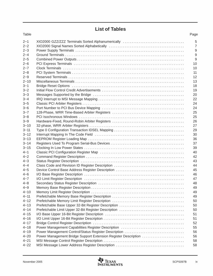
List of TablesTable Page
2−1 XIO2000 GZZ/ZZZ Terminals Sorted Alphanumerically 5 . . . . . . . . . . . . . . . . . . . . . . . . . . . . . . . . . . . 2−2 XIO2000 Signal Names Sorted Alphabetically 7 . . . . . . . . . . . . . . . . . . . . . . . . . . . . . . . . . . . . . . . . . . . 2−3 Power Supply Terminals 9 . . . . . . . . . . . . . . . . . . . . . . . . . . . . . . . . . . . . . . . . . . . . . . . . . . . . . . . . . . . . . . 2−4 Ground Terminals 9 . . . . . . . . . . . . . . . . . . . . . . . . . . . . . . . . . . . . . . . . . . . . . . . . . . . . . . . . . . . . . . . . . . . . 2−5 Combined Power Outputs 9 . . . . . . . . . . . . . . . . . . . . . . . . . . . . . . . . . . . . . . . . . . . . . . . . . . . . . . . . . . . . . 2−6 PCI Express Terminals 10 . . . . . . . . . . . . . . . . . . . . . . . . . . . . . . . . . . . . . . . . . . . . . . . . . . . . . . . . . . . . . . . 2−7 Clock Terminals 10 . . . . . . . . . . . . . . . . . . . . . . . . . . . . . . . . . . . . . . . . . . . . . . . . . . . . . . . . . . . . . . . . . . . . . 2−8 PCI System Terminals 11 . . . . . . . . . . . . . . . . . . . . . . . . . . . . . . . . . . . . . . . . . . . . . . . . . . . . . . . . . . . . . . . . 2−9 Reserved Terminals 12 . . . . . . . . . . . . . . . . . . . . . . . . . . . . . . . . . . . . . . . . . . . . . . . . . . . . . . . . . . . . . . . . . . 2−10 Miscellaneous Terminals 13 . . . . . . . . . . . . . . . . . . . . . . . . . . . . . . . . . . . . . . . . . . . . . . . . . . . . . . . . . . . . . . 3−1 Bridge Reset Options 18 . . . . . . . . . . . . . . . . . . . . . . . . . . . . . . . . . . . . . . . . . . . . . . . . . . . . . . . . . . . . . . . . 3−2 Initial Flow Control Credit Advertisements 19 . . . . . . . . . . . . . . . . . . . . . . . . . . . . . . . . . . . . . . . . . . . . . . . 3−3 Messages Supported by the Bridge 20 . . . . . . . . . . . . . . . . . . . . . . . . . . . . . . . . . . . . . . . . . . . . . . . . . . . . 3−4 IRQ Interrupt to MSI Message Mapping 22 . . . . . . . . . . . . . . . . . . . . . . . . . . . . . . . . . . . . . . . . . . . . . . . . . 3−5 Classic PCI Arbiter Registers 24 . . . . . . . . . . . . . . . . . . . . . . . . . . . . . . . . . . . . . . . . . . . . . . . . . . . . . . . . . . 3−6 Port Number to PCI Bus Device Mapping 24 . . . . . . . . . . . . . . . . . . . . . . . . . . . . . . . . . . . . . . . . . . . . . . . 3−7 128-Phase, WRR Time-Based Arbiter Registers 25 . . . . . . . . . . . . . . . . . . . . . . . . . . . . . . . . . . . . . . . . . 3−8 PCI Isochronous Windows 25 . . . . . . . . . . . . . . . . . . . . . . . . . . . . . . . . . . . . . . . . . . . . . . . . . . . . . . . . . . . . 3−9 Hardware-Fixed, Round-Robin Arbiter Registers 26 . . . . . . . . . . . . . . . . . . . . . . . . . . . . . . . . . . . . . . . . . 3−10 32-phase, WRR Arbiter Registers 27 . . . . . . . . . . . . . . . . . . . . . . . . . . . . . . . . . . . . . . . . . . . . . . . . . . . . . . 3−11 Type 0 Configuration Transaction IDSEL Mapping 29 . . . . . . . . . . . . . . . . . . . . . . . . . . . . . . . . . . . . . . . . 3−12 Interrupt Mapping In The Code Field 30 . . . . . . . . . . . . . . . . . . . . . . . . . . . . . . . . . . . . . . . . . . . . . . . . . . . 3−13 EEPROM Register Loading Map 36 . . . . . . . . . . . . . . . . . . . . . . . . . . . . . . . . . . . . . . . . . . . . . . . . . . . . . . . 3−14 Registers Used To Program Serial-Bus Devices 37 . . . . . . . . . . . . . . . . . . . . . . . . . . . . . . . . . . . . . . . . . . 3−15 Clocking In Low Power States 39 . . . . . . . . . . . . . . . . . . . . . . . . . . . . . . . . . . . . . . . . . . . . . . . . . . . . . . . . . 4−1 Classic PCI Configuration Register Map 40 . . . . . . . . . . . . . . . . . . . . . . . . . . . . . . . . . . . . . . . . . . . . . . . . 4−2 Command Register Description 42 . . . . . . . . . . . . . . . . . . . . . . . . . . . . . . . . . . . . . . . . . . . . . . . . . . . . . . . . 4−3 Status Register Description 43 . . . . . . . . . . . . . . . . . . . . . . . . . . . . . . . . . . . . . . . . . . . . . . . . . . . . . . . . . . . 4−4 Class Code and Revision ID Register Description 44 . . . . . . . . . . . . . . . . . . . . . . . . . . . . . . . . . . . . . . . . 4−5 Device Control Base Address Register Description 45 . . . . . . . . . . . . . . . . . . . . . . . . . . . . . . . . . . . . . . . 4−6 I/O Base Register Description 46 . . . . . . . . . . . . . . . . . . . . . . . . . . . . . . . . . . . . . . . . . . . . . . . . . . . . . . . . . 4−7 I/O Limit Register Description 47 . . . . . . . . . . . . . . . . . . . . . . . . . . . . . . . . . . . . . . . . . . . . . . . . . . . . . . . . . 4−8 Secondary Status Register Description 48 . . . . . . . . . . . . . . . . . . . . . . . . . . . . . . . . . . . . . . . . . . . . . . . . . 4−9 Memory Base Register Description 49 . . . . . . . . . . . . . . . . . . . . . . . . . . . . . . . . . . . . . . . . . . . . . . . . . . . . . 4−10 Memory Limit Register Description 49 . . . . . . . . . . . . . . . . . . . . . . . . . . . . . . . . . . . . . . . . . . . . . . . . . . . . . 4−11 Prefetchable Memory Base Register Description 49 . . . . . . . . . . . . . . . . . . . . . . . . . . . . . . . . . . . . . . . . . 4−12 Prefetchable Memory Limit Register Description 50 . . . . . . . . . . . . . . . . . . . . . . . . . . . . . . . . . . . . . . . . . 4−13 Prefetchable Base Upper 32-Bit Register Description 50 . . . . . . . . . . . . . . . . . . . . . . . . . . . . . . . . . . . . . 4−14 Prefetchable Limit Upper 32-Bit Register Description 50 . . . . . . . . . . . . . . . . . . . . . . . . . . . . . . . . . . . . . 4−15 I/O Base Upper 16-Bit Register Description 51 . . . . . . . . . . . . . . . . . . . . . . . . . . . . . . . . . . . . . . . . . . . . . 4−16 I/O Limit Upper 16-Bit Register Description 51 . . . . . . . . . . . . . . . . . . . . . . . . . . . . . . . . . . . . . . . . . . . . . . 4−17 Bridge Control Register Description 52 . . . . . . . . . . . . . . . . . . . . . . . . . . . . . . . . . . . . . . . . . . . . . . . . . . . . 4−18 Power Management Capabilities Register Description 55 . . . . . . . . . . . . . . . . . . . . . . . . . . . . . . . . . . . . 4−19 Power Management Control/Status Register Description 56 . . . . . . . . . . . . . . . . . . . . . . . . . . . . . . . . . . 4−20 Power Management Bridge Support Extension Register Description 56 . . . . . . . . . . . . . . . . . . . . . . . . 4−21 MSI Message Control Register Description 58 . . . . . . . . . . . . . . . . . . . . . . . . . . . . . . . . . . . . . . . . . . . . . . 4−22 MSI Message Lower Address Register Description 58 . . . . . . . . . . . . . . . . . . . . . . . . . . . . . . . . . . . . . . .

Tables
x November 2005SCPS097B
Table Page
4−23 MSI Message Data Register Description 59 . . . . . . . . . . . . . . . . . . . . . . . . . . . . . . . . . . . . . . . . . . . . . . . . 4−24 PCI Express Capabilities Register Description 61 . . . . . . . . . . . . . . . . . . . . . . . . . . . . . . . . . . . . . . . . . . . 4−25 Device Capabilities Register Description 62 . . . . . . . . . . . . . . . . . . . . . . . . . . . . . . . . . . . . . . . . . . . . . . . . 4−26 Device Control Register Description 63 . . . . . . . . . . . . . . . . . . . . . . . . . . . . . . . . . . . . . . . . . . . . . . . . . . . . 4−27 Device Status Register Description 64 . . . . . . . . . . . . . . . . . . . . . . . . . . . . . . . . . . . . . . . . . . . . . . . . . . . . . 4−28 Link Capabilities Register Description 65 . . . . . . . . . . . . . . . . . . . . . . . . . . . . . . . . . . . . . . . . . . . . . . . . . . 4−29 Link Control Register Description 66 . . . . . . . . . . . . . . . . . . . . . . . . . . . . . . . . . . . . . . . . . . . . . . . . . . . . . . 4−30 Link Status Register Description 67 . . . . . . . . . . . . . . . . . . . . . . . . . . . . . . . . . . . . . . . . . . . . . . . . . . . . . . . 4−31 Serial-Bus Slave Address Register Description 68 . . . . . . . . . . . . . . . . . . . . . . . . . . . . . . . . . . . . . . . . . . 4−32 Serial-Bus Control and Status Register Description 69 . . . . . . . . . . . . . . . . . . . . . . . . . . . . . . . . . . . . . . . 4−33 GPIO Control Register Description 70 . . . . . . . . . . . . . . . . . . . . . . . . . . . . . . . . . . . . . . . . . . . . . . . . . . . . . 4−34 GPIO Data Register Description 71 . . . . . . . . . . . . . . . . . . . . . . . . . . . . . . . . . . . . . . . . . . . . . . . . . . . . . . . 4−35 Control and Diagnostic Register 0 Description 72 . . . . . . . . . . . . . . . . . . . . . . . . . . . . . . . . . . . . . . . . . . . 4−36 Control and Diagnostic Register 1 Description 73 . . . . . . . . . . . . . . . . . . . . . . . . . . . . . . . . . . . . . . . . . . . 4−37 Control and Diagnostic Register 2 Description 74 . . . . . . . . . . . . . . . . . . . . . . . . . . . . . . . . . . . . . . . . . . . 4−38 Subsystem Access Register Description 74 . . . . . . . . . . . . . . . . . . . . . . . . . . . . . . . . . . . . . . . . . . . . . . . . 4−39 General Control Register Description 75 . . . . . . . . . . . . . . . . . . . . . . . . . . . . . . . . . . . . . . . . . . . . . . . . . . . 4−40 Clock Control Register Description 77 . . . . . . . . . . . . . . . . . . . . . . . . . . . . . . . . . . . . . . . . . . . . . . . . . . . . . 4−41 Clock Mask Register Description 78 . . . . . . . . . . . . . . . . . . . . . . . . . . . . . . . . . . . . . . . . . . . . . . . . . . . . . . . 4−42 Clock Run Status Register Description 79 . . . . . . . . . . . . . . . . . . . . . . . . . . . . . . . . . . . . . . . . . . . . . . . . . 4−43 Arbiter Control Register Description 80 . . . . . . . . . . . . . . . . . . . . . . . . . . . . . . . . . . . . . . . . . . . . . . . . . . . . 4−44 Arbiter Request Mask Register Description 81 . . . . . . . . . . . . . . . . . . . . . . . . . . . . . . . . . . . . . . . . . . . . . . 4−45 Arbiter Time-Out Status Register Description 82 . . . . . . . . . . . . . . . . . . . . . . . . . . . . . . . . . . . . . . . . . . . . 4−46 Serial IRQ Mode Control Register Description 83 . . . . . . . . . . . . . . . . . . . . . . . . . . . . . . . . . . . . . . . . . . . 4−47 Serial IRQ Edge Control Register Description 84 . . . . . . . . . . . . . . . . . . . . . . . . . . . . . . . . . . . . . . . . . . . . 4−48 Serial IRQ Status Register Description 85 . . . . . . . . . . . . . . . . . . . . . . . . . . . . . . . . . . . . . . . . . . . . . . . . . 5−1 PCI Express Extended Configuration Register Map 87 . . . . . . . . . . . . . . . . . . . . . . . . . . . . . . . . . . . . . . . 5−2 Uncorrectable Error Status Register Description 89 . . . . . . . . . . . . . . . . . . . . . . . . . . . . . . . . . . . . . . . . . 5−3 Uncorrectable Error Mask Register Description 90 . . . . . . . . . . . . . . . . . . . . . . . . . . . . . . . . . . . . . . . . . . 5−4 Uncorrectable Error Severity Register Description 91 . . . . . . . . . . . . . . . . . . . . . . . . . . . . . . . . . . . . . . . . 5−5 Correctable Error Status Register Description 92 . . . . . . . . . . . . . . . . . . . . . . . . . . . . . . . . . . . . . . . . . . . 5−6 Correctable Error Mask Register Description 93 . . . . . . . . . . . . . . . . . . . . . . . . . . . . . . . . . . . . . . . . . . . . 5−7 Advanced Error Capabilities and Control Register Description 94 . . . . . . . . . . . . . . . . . . . . . . . . . . . . . 5−8 Secondary Uncorrectable Error Status Register Description 95 . . . . . . . . . . . . . . . . . . . . . . . . . . . . . . . 5−9 Secondary Uncorrectable Error Mask Register Description 96 . . . . . . . . . . . . . . . . . . . . . . . . . . . . . . . . 5−10 Secondary Uncorrectable Error Severity Register Description 97 . . . . . . . . . . . . . . . . . . . . . . . . . . . . . . 5−11 Secondary Error Capabilities and Control Register Description 98 . . . . . . . . . . . . . . . . . . . . . . . . . . . . . 5−12 Secondary Header Log Register Description 99 . . . . . . . . . . . . . . . . . . . . . . . . . . . . . . . . . . . . . . . . . . . . 5−13 Port VC Capability Register 1 Description 100 . . . . . . . . . . . . . . . . . . . . . . . . . . . . . . . . . . . . . . . . . . . . . . . 5−14 Port VC Capability Register 2 Description 101 . . . . . . . . . . . . . . . . . . . . . . . . . . . . . . . . . . . . . . . . . . . . . . . 5−15 Port VC Control Register Description 102 . . . . . . . . . . . . . . . . . . . . . . . . . . . . . . . . . . . . . . . . . . . . . . . . . . . 5−16 Port VC Status Register Description 102 . . . . . . . . . . . . . . . . . . . . . . . . . . . . . . . . . . . . . . . . . . . . . . . . . . . . 5−17 VC Resource Capability Register (VC0) Description 103 . . . . . . . . . . . . . . . . . . . . . . . . . . . . . . . . . . . . . . 5−18 VC Resource Control Register (VC0) Description 104 . . . . . . . . . . . . . . . . . . . . . . . . . . . . . . . . . . . . . . . . 5−19 VC Resource Status Register (VC0) Description 105 . . . . . . . . . . . . . . . . . . . . . . . . . . . . . . . . . . . . . . . . . 5−20 VC Resource Capability Register (VC1) Description 105 . . . . . . . . . . . . . . . . . . . . . . . . . . . . . . . . . . . . . . 5−21 VC Resource Control Register (VC1) Description 106 . . . . . . . . . . . . . . . . . . . . . . . . . . . . . . . . . . . . . . . . 5−22 VC Resource Status Register (VC1) Description 107 . . . . . . . . . . . . . . . . . . . . . . . . . . . . . . . . . . . . . . . . .

xiNovember 2005 SCPS097B
Table Page
5−23 VC Arbitration Table 107 . . . . . . . . . . . . . . . . . . . . . . . . . . . . . . . . . . . . . . . . . . . . . . . . . . . . . . . . . . . . . . . . . . 5−24 VC Arbitration Table Entry Description 107 . . . . . . . . . . . . . . . . . . . . . . . . . . . . . . . . . . . . . . . . . . . . . . . . . . 5−25 Port Arbitration Table 108 . . . . . . . . . . . . . . . . . . . . . . . . . . . . . . . . . . . . . . . . . . . . . . . . . . . . . . . . . . . . . . . . . 5−26 Port Arbitration Table Entry Description 108 . . . . . . . . . . . . . . . . . . . . . . . . . . . . . . . . . . . . . . . . . . . . . . . . . 6−1 Device Control Memory Window Register Map 109 . . . . . . . . . . . . . . . . . . . . . . . . . . . . . . . . . . . . . . . . . . . 6−2 Upstream Isochronous Capabilities Register Description 110 . . . . . . . . . . . . . . . . . . . . . . . . . . . . . . . . . . 6−3 Upstream Isochrony Control Register Description 111 . . . . . . . . . . . . . . . . . . . . . . . . . . . . . . . . . . . . . . . . 6−4 Upstream Isochronous Window 0 Control Register Description 112 . . . . . . . . . . . . . . . . . . . . . . . . . . . . . 6−5 Upstream Isochronous Window 1 Control Register Description 113 . . . . . . . . . . . . . . . . . . . . . . . . . . . . . 6−6 Upstream Isochronous Window 2 Control Register Description 114 . . . . . . . . . . . . . . . . . . . . . . . . . . . . . 6−7 Upstream Isochronous Window 3 Control Register Description 115 . . . . . . . . . . . . . . . . . . . . . . . . . . . . . 6−8 GPIO Control Register Description 116 . . . . . . . . . . . . . . . . . . . . . . . . . . . . . . . . . . . . . . . . . . . . . . . . . . . . . 6−9 GPIO Data Register Description 117 . . . . . . . . . . . . . . . . . . . . . . . . . . . . . . . . . . . . . . . . . . . . . . . . . . . . . . . 6−10 Serial-Bus Slave Address Register Description 118 . . . . . . . . . . . . . . . . . . . . . . . . . . . . . . . . . . . . . . . . . . 6−11 Serial-Bus Control and Status Register Description 119 . . . . . . . . . . . . . . . . . . . . . . . . . . . . . . . . . . . . . . . 6−12 Serial IRQ Mode Control Register Description 120 . . . . . . . . . . . . . . . . . . . . . . . . . . . . . . . . . . . . . . . . . . . 6−13 Serial IRQ Edge Control Register Description 121 . . . . . . . . . . . . . . . . . . . . . . . . . . . . . . . . . . . . . . . . . . . . 6−14 Serial IRQ Status Register Description 122 . . . . . . . . . . . . . . . . . . . . . . . . . . . . . . . . . . . . . . . . . . . . . . . . .

Tables
xii November 2005SCPS097B
(This page has been left blank intentionally.)
Features
1November 2005 SCPS097B
1 XIO2000 Features Full x1 PCI Express Throughput
Fully Compliant with PCI Express toPCI/PCI-X Bridge Specification,Revision 1.0
Fully Compliant with PCI Express BaseSpecification, Revision 1.0a
Fully Compliant with PCI Local BusSpecification, Revision 2.3
Extended Virtual Channel (VC) SupportIncludes a Second VC forQuality-of-Service and IsochronousApplications
PCI Express Advanced Error ReportingCapability Including ECRC Support
Support for D1, D2, D3 hot , and D3cold Active State Link Power Management
Saves Power When Packet Activity on thePCI Express Link is Idle, Using Both L0sand L1 States
Wake Event and Beacon Support
Error Forwarding Including PCI ExpressData Poisoning and PCI Bus Parity Errors
Utilizes 100-MHz Differential PCI ExpressCommon Reference Clock or 125-MHzSingle-Ended, Reference Clock
Robust Pipeline Architecture To MinimizeTransaction Latency
Full PCI Local Bus 66-MHz/32-BitThroughput
Support for Six Subordinate PCI BusMasters with Internal Configurable, 2-LevelPrioritization Scheme
Advanced VC Arbitration Options IncludeVC1 Strict Priority, Hardware-FixedRound-Robin, and 32-Phase, WeightedRound-Robin
Advanced PCI Bus Port Arbitration OptionsInclude 128-phase, Weighted Round-RobinTime-Based and 128-phase, WeightedRound-Robin Aggressive Time-Based
Advanced PCI Isochronous Windows forMemory Space Mapping to a SpecifiedTraffic Class
Advanced PCI Express Message SignaledInterrupt Generation for Serial IRQInterrupts from CardBus Applications
External PCI Bus Arbiter Option
PCI Bus LOCK Support
Clock Run and Power Override Support
Six Buffered PCI Clock Outputs (33 MHz or66 MHz)
PCI Bus Interface 3.3-V and 5.0-V (33 MHzonly at 5.0 V) Tolerance Options
Integrated AUX Power Switch Drains V AUXPower Only When Main Power Is Off
Eight 3.3-V, Multifunction, General-PurposeI/O Terminals
Memory-Mapped EEPROM Serial-BusController Supporting PCI Express PowerBudget/Limit Extensions for Add-In Cards
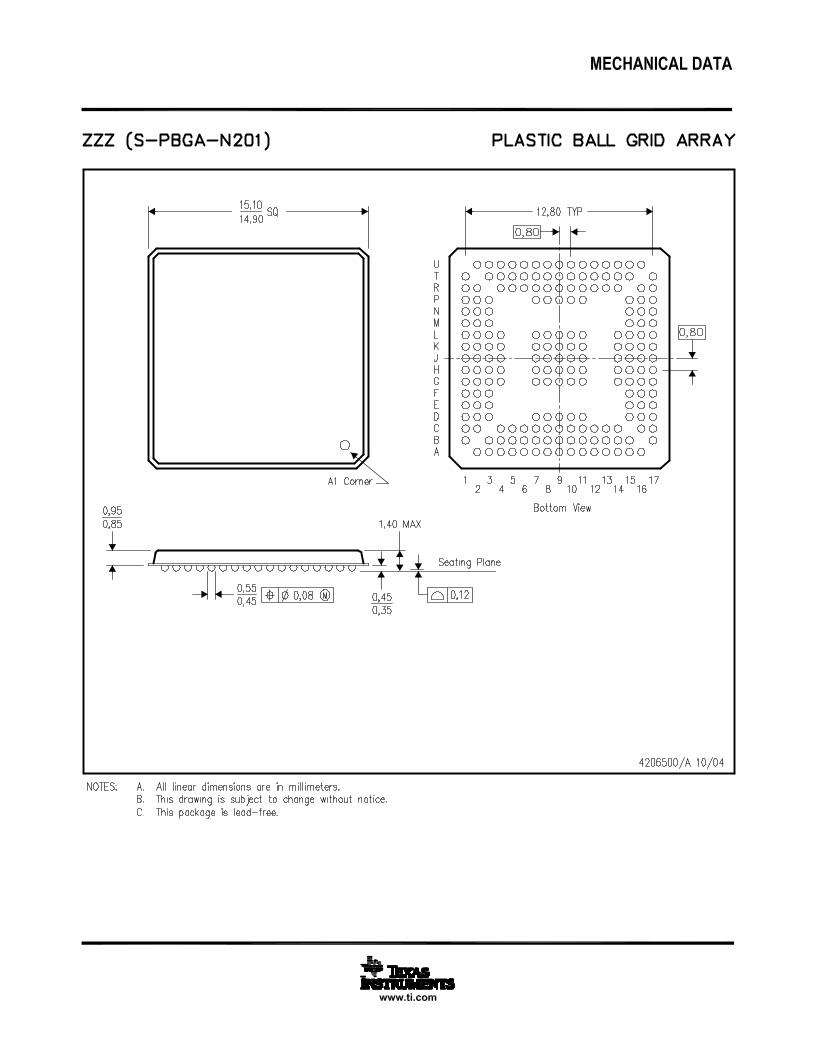
Compact Footprint, 201-Ball, GZZMicroStar TM BGA or Lead-Free 201-Ball,ZZZ MicroStar TM BGA
Table 1−1.
Figure 1−1.
MicroStar BGA is a trademark of Texas Instruments.Other trademarks are the property of their respective owners.

Introduction
2 November 2005SCPS097B
2 IntroductionThe Texas Instruments XIO2000 is a PCI Express to PCI local bus translation bridge that provides full PCIExpress and PCI local bus functionality and performance.
2.1 Description
The XIO2000 is a single-function PCI Express to PCI translation bridge that is fully compliant to the PCIExpress to PCI/PCI-X Bridge Specification, Revision 1.0. For downstream traffic, the bridge simultaneouslysupports up to eight posted and four nonposted transactions for each enabled virtual channel (VC). Forupstream traffic, up to six posted and four nonposted transactions are simultaneously supported for each VC.
The PCI Express interface is fully compliant to the PCI Express Base Specification, Revision 1.0a.
The PCI Express interface supports a x1 link operating at full 250 MB/s packet throughput in each directionsimultaneously. Two independent VCs are supported. The second VC is optimized for isochronous traffictypes and quality-of-service (QoS) applications. Also, the bridge supports the advanced error reportingcapability including extended CRC (ECRC) as defined in the PCI Express Base Specification. Supplementalfirmware or software is required to fully utilize both of these features.
Robust pipeline architecture is implemented to minimize system latency across the bridge. If parity errors aredetected, then packet poisoning is supported for both upstream and downstream operations.
The PCI local bus is fully compliant with the PCI Local Bus Specification (Revision 2.3) and associatedprogramming model. Also, the bridge supports the standard PCI-to-PCI bridge programming model.
The PCI bus interface is 32-bit and can operate at either 33 MHz or 66 MHz. Also, the PCI interface providesfair arbitration and buffered clock outputs for up to 6 subordinate devices. The bridge has advanced VCarbitration and PCI port arbitration features for upstream traffic. When these arbitration features are fullyutilized, bridge throughput performance may be tuned for a variety of complex applications.
Power management (PM) features include active state link PM, PME mechanisms, the beacon and wakeprotocols, and all conventional PCI D-states. If the active state link PM is enabled, then the link automaticallysaves power when idle using the L0s and L1 states. PM active state NAK, PM PME, and PME-to-ACKmessages are supported. Standard PCI bus power management features provide several low power modes,which enable the host system to further reduce power consumption.
The bridge has additional capabilities including, but not limited to, serial IRQ with MSI messages, serialEEPROM, power override, clock run, and PCI bus LOCK. Also, eight general-purpose inputs and outputs(GPIOs) are provided for further system control and customization.
2.2 Related Documents• PCI Express to PCI/PCI-X Bridge Specification, Revision 1.0• PCI Express Base Specification, Revision 1.0a• PCI Express Card Electromechanical Specification, Revision 1.0a• PCI Local Bus Specification, Revision 2.3• PCI-to-PCI Bridge Architecture Specification, Revision 1.2• PCI Bus Power Management Interface Specification, Revision 1.1 or 1.2• PCI Mobile Design Guide, Revision 1.1• Serialized IRQ Support for PCI Systems, Revision 6.0• PCI Express Jitter and BER White Paper
2.3 Trademarks• PCI Express is a trademark of PCI-SIG• TI and MicroStar BGA are trademarks of Texas Instruments• Other trademarks are the property of their respective owners
Introduction
3November 2005 SCPS097B
2.4 Document Conventions
Throughout this data manual, several conventions are used to convey information. These conventions arelisted below:
1. To identify a binary number or field, a lower case b follows the numbers. For example: 000b is a 3-bit binaryfield.
2. To identify a hexadecimal number or field, a lower case h follows the numbers. For example: 8AFh is a12-bit hexadecimal field.
3. All other numbers that appear in this document that do not have either a b or h following the number areassumed to be decimal format.
4. If the signal or terminal name has a bar above the name (for example, GRST), then this indicates thelogical NOT function. When asserted, this signal is a logic low, 0, or 0b.
5. Differential signal names end with P, N, +, or − designators. The P or + designators signify the positivesignal associated with the differential pair. The N or − designators signify the negative signal associatedwith the differential pair.
6. RSVD indicates that the referenced item is reserved.
7. The power and ground signals in Figure 2−1 are not subscripted to aid in readability.
8. In Sections 4 through 6, the configuration space for the bridge is defined. For each register bit, the softwareaccess method is identified in an access column. The legend for this access column includes the followingentries:
r – read access by software
u – updates by the bridge internal hardware
w – write access by software
c – clear an asserted status bit with a write-back of 1b by software
2.5 Document History
REVISIONDATE
REVISIONNUMBER REVISION COMMENTS
05/2004 − Product preview
08/2005 A Initial release
2.6 Ordering Information
ORDERING NUMBER NAME VOLTAGE PACKAGE
XIO2000 PCI-Express to PCI Bridge 3.3-V, 5.0-V tolerant PCI busI/Os with 3.3-V and 1.5-V power
terminals
201-terminal GZZ MicroStarPBGA
XIO2000 PCI-Express to PCI Bridge 3.3-V, 5.0-V tolerant PCI busI/Os with 3.3-V and 1.5-V power
terminals
201-terminal ZZZ (Lead-Free)MicroStar PBGA
Introduction
4 November 2005SCPS097B
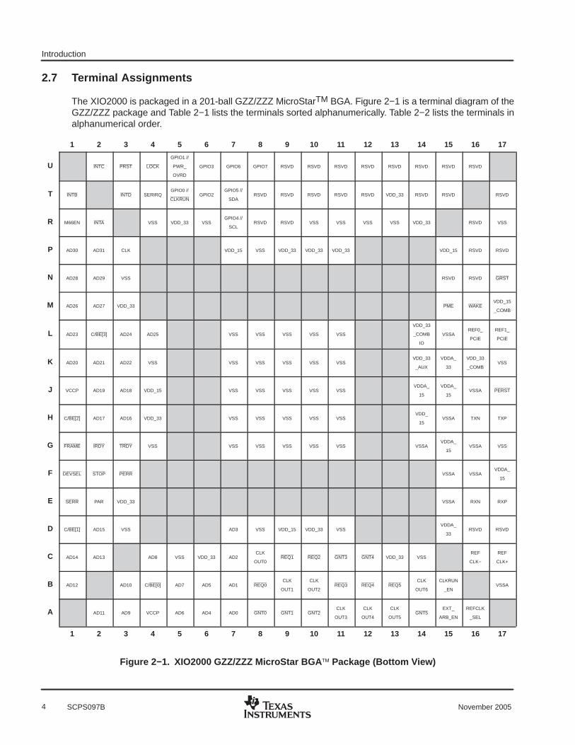
2.7 Terminal Assignments
The XIO2000 is packaged in a 201-ball GZZ/ZZZ MicroStarTM BGA. Figure 2−1 is a terminal diagram of theGZZ/ZZZ package and Table 2−1 lists the terminals sorted alphanumerically. Table 2−2 lists the terminals inalphanumerical order.
1 2 3 4 5 6 7 8 9 10 11 12 13 14 15 16 17
U INTC PRST LOCK
GPIO1 //
PWR_
OVRD
GPIO3 GPIO6 GPIO7 RSVD RSVD RSVD RSVD RSVD RSVD RSVD RSVD
T INTB INTD SERIRQGPIO0 //
CLKRUNGPIO2
GPIO5 //
SDARSVD RSVD RSVD RSVD RSVD VDD_33 RSVD RSVD RSVD
R M66EN INTA VSS VDD_33 VSSGPIO4 //
SCLRSVD RSVD VSS VSS VSS VSS VDD_33 RSVD VSS
P AD30 AD31 CLK VDD_15 VSS VDD_33 VDD_33 VDD_33 VDD_15 RSVD RSVD
N AD28 AD29 VSS RSVD RSVD GRST
M AD26 AD27 VDD_33 PME WAKEVDD_15
_COMB
L AD23 C/BE[3] AD24 AD25 VSS VSS VSS VSS VSS
VDD_33
_COMB
IO
VSSAREF0_
PCIE
REF1_
PCIE
K AD20 AD21 AD22 VSS VSS VSS VSS VSS VSSVDD_33
_AUX
VDDA_
33
VDD_33
_COMBVSS
J VCCP AD19 AD18 VDD_15 VSS VSS VSS VSS VSSVDDA_
15
VDDA_
15VSSA PERST
H C/BE[2] AD17 AD16 VDD_33 VSS VSS VSS VSS VSSVDD_
15VSSA TXN TXP
G FRAME IRDY TRDY VSS VSS VSS VSS VSS VSS VSSAVDDA_
15VSSA VSS
F DEVSEL STOP PERR VSSA VSSAVDDA_
15
E SERR PAR VDD_33 VSSA RXN RXP
D C/BE[1] AD15 VSS AD3 VSS VDD_15 VDD_33 VSSVDDA_
33RSVD RSVD
C AD14 AD13 AD8 VSS VDD_33 AD2CLK
OUT0REQ1 REQ2 GNT3 GNT4 VDD_33 VSS
REF
CLK−
REF
CLK+
B AD12 AD10 C/BE[0] AD7 AD5 AD1 REQ0CLK
OUT1
CLK
OUT2REQ3 REQ4 REQ5
CLK
OUT6
CLKRUN
_ENVSSA
A AD11 AD9 VCCP AD6 AD4 AD0 GNT0 GNT1 GNT2CLK
OUT3
CLK
OUT4
CLK
OUT5GNT5
EXT_
ARB_EN
REFCLK
_SEL
1 2 3 4 5 6 7 8 9 10 11 12 13 14 15 16 17
Figure 2−1. XIO2000 GZZ/ZZZ MicroStar BGA Package (Bottom View)
Introduction
5November 2005 SCPS097B
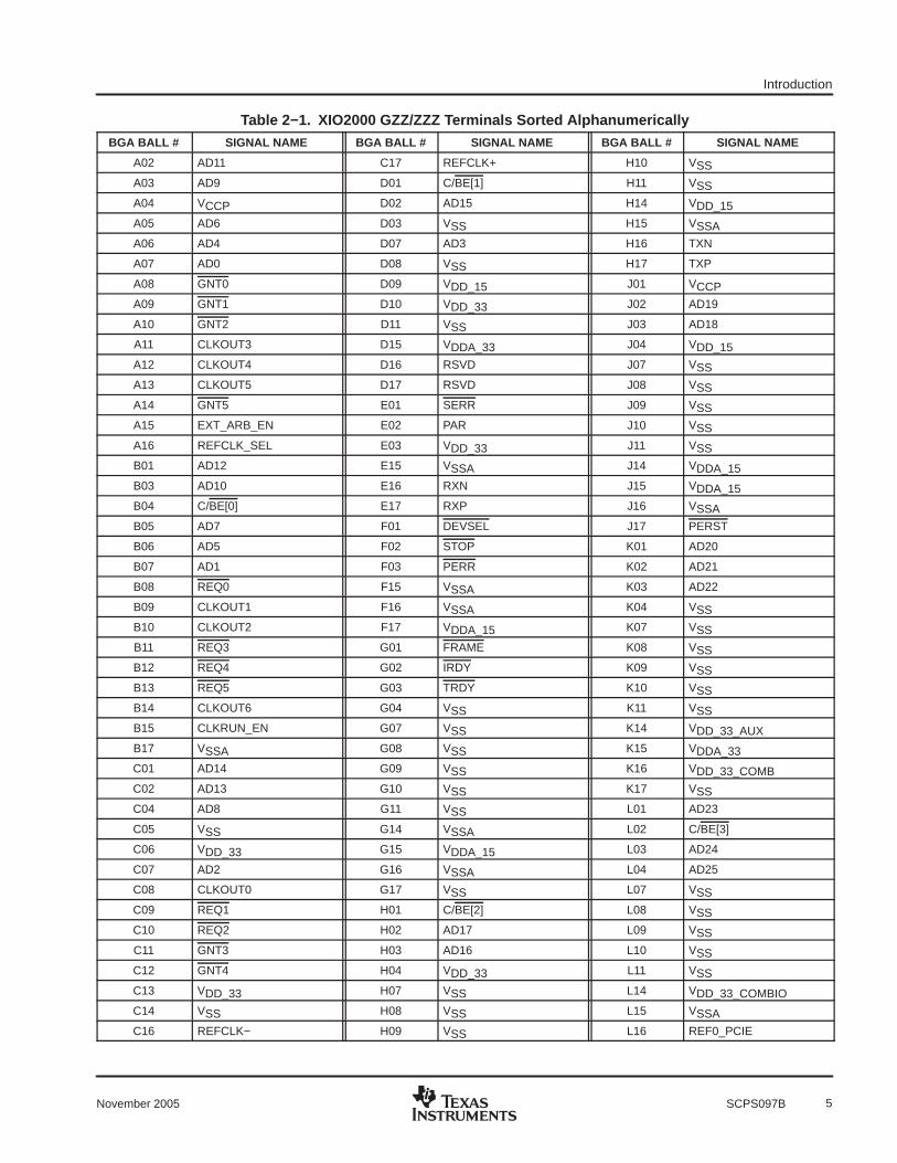
Table 2−1. XIO2000 GZZ/ZZZ Terminals Sorted AlphanumericallyBGA BALL # SIGNAL NAME BGA BALL # SIGNAL NAME BGA BALL # SIGNAL NAME
A02 AD11 C17 REFCLK+ H10 VSS
A03 AD9 D01 C/BE[1] H11 VSS
A04 VCCP D02 AD15 H14 VDD_15
A05 AD6 D03 VSS H15 VSSA
A06 AD4 D07 AD3 H16 TXN
A07 AD0 D08 VSS H17 TXP
A08 GNT0 D09 VDD_15 J01 VCCP
A09 GNT1 D10 VDD_33 J02 AD19
A10 GNT2 D11 VSS J03 AD18
A11 CLKOUT3 D15 VDDA_33 J04 VDD_15
A12 CLKOUT4 D16 RSVD J07 VSS
A13 CLKOUT5 D17 RSVD J08 VSS
A14 GNT5 E01 SERR J09 VSS
A15 EXT_ARB_EN E02 PAR J10 VSS
A16 REFCLK_SEL E03 VDD_33 J11 VSS
B01 AD12 E15 VSSA J14 VDDA_15
B03 AD10 E16 RXN J15 VDDA_15
B04 C/BE[0] E17 RXP J16 VSSA
B05 AD7 F01 DEVSEL J17 PERST
B06 AD5 F02 STOP K01 AD20
B07 AD1 F03 PERR K02 AD21
B08 REQ0 F15 VSSA K03 AD22
B09 CLKOUT1 F16 VSSA K04 VSS
B10 CLKOUT2 F17 VDDA_15 K07 VSS
B11 REQ3 G01 FRAME K08 VSS
B12 REQ4 G02 IRDY K09 VSS
B13 REQ5 G03 TRDY K10 VSS
B14 CLKOUT6 G04 VSS K11 VSS
B15 CLKRUN_EN G07 VSS K14 VDD_33_AUX
B17 VSSA G08 VSS K15 VDDA_33
C01 AD14 G09 VSS K16 VDD_33_COMB
C02 AD13 G10 VSS K17 VSS
C04 AD8 G11 VSS L01 AD23
C05 VSS G14 VSSA L02 C/BE[3]
C06 VDD_33 G15 VDDA_15 L03 AD24
C07 AD2 G16 VSSA L04 AD25
C08 CLKOUT0 G17 VSS L07 VSS
C09 REQ1 H01 C/BE[2] L08 VSS
C10 REQ2 H02 AD17 L09 VSS
C11 GNT3 H03 AD16 L10 VSS
C12 GNT4 H04 VDD_33 L11 VSS
C13 VDD_33 H07 VSS L14 VDD_33_COMBIO
C14 VSS H08 VSS L15 VSSA
C16 REFCLK− H09 VSS L16 REF0_PCIE

Introduction
6 November 2005SCPS097B
Table 2−1. XIO2000 GZZ/ZZZ Terminals Sorted Alphanumerically (Continued)BGA BALL # SIGNAL NAME BGA BALL # SIGNAL NAME BGA BALL # SIGNAL NAME
L17 REF1_PCIE P17 RSVD T09 RSVD
M01 AD26 R01 M66EN T10 RSVD
M02 AD27 R02 INTA T11 RSVD
M03 VDD_33 R04 VSS T12 RSVD
M15 PME R05 VDD_33 T13 VDD_33
M16 WAKE R06 VSS T14 RSVD
M17 VDD_15_COMB R07 GPIO4 // SCL T15 RSVD
N01 AD28 R08 RSVD T17 RSVD
N02 AD29 R09 RSVD U02 INTC
N03 VSS R10 VSS U03 PRST
N15 RSVD R11 VSS U04 LOCK
N16 RSVD R12 VSS U05 GPIO1 // PWR_OVRD
N17 GRST R13 VSS U06 GPIO3
P01 AD30 R14 VDD_33 U07 GPIO6
P02 AD31 R16 RSVD U08 GPIO7
P03 CLK R17 VSS U09 RSVD
P07 VDD_15 T01 INTB U10 RSVD
P08 VSS T03 INTD U11 RSVD
P09 VDD_33 T04 SERIRQ U12 RSVD
P10 VDD_33 T05 GPIO0 // CLKRUN U13 RSVD
P11 VDD_33 T06 GPIO2 U14 RSVD
P15 VDD_15 T07 GPIO5 // SDA U15 RSVD
P16 RSVD T08 RSVD U16 RSVD

Introduction
7November 2005 SCPS097B
Table 2−2. XIO2000 Signal Names Sorted AlphabeticallySIGNAL NAME BGA BALL # SIGNAL NAME BGA BALL # SIGNAL NAME BGA BALL #
AD0 A07 CLKRUN_EN B15 RSVD N15
AD1 B07 DEVSEL F01 RSVD N16
AD2 C07 EXT_ARB_EN A15 RSVD P16
AD3 D07 FRAME G01 RSVD P17
AD4 A06 GNT0 A08 RSVD R08
AD5 B06 GNT1 A09 RSVD R09
AD6 A05 GNT2 A10 RSVD R16
AD7 B05 GNT3 C11 RSVD T08
AD8 C04 GNT4 C12 RSVD T09
AD9 A03 GNT5 A14 RSVD T10
AD10 B03 GPIO0 // CLKRUN T05 RSVD T11
AD11 A02 GPIO1 // PWR_OVRD U05 RSVD T12
AD12 B01 GPIO2 T06 RSVD T14
AD13 C02 GPIO3 U06 RSVD T15
AD14 C01 GPIO4 // SCL R07 RSVD T17
AD15 D02 GPIO5 // SDA T07 RSVD U09
AD16 H03 GPIO6 U07 RSVD U10
AD17 H02 GPIO7 U08 RSVD U11
AD18 J03 GRST N17 RSVD U12
AD19 J02 INTA R02 RSVD U13
AD20 K01 INTB T01 RSVD U14
AD21 K02 INTC U02 RSVD U15
AD22 K03 INTD T03 RSVD U16
AD23 L01 IRDY G02 RXN E16
AD24 L03 LOCK U04 RXP E17
AD25 L04 M66EN R01 SERIRQ T04
AD26 M01 PAR E02 SERR E01
AD27 M02 PERR F03 STOP F02
AD28 N01 PERST J17 TRDY G03
AD29 N02 PME M15 TXN H16
AD30 P01 PRST U03 TXP H17
AD31 P02 REF0_PCIE L16 VCCP A04
C/BE[0] B04 REF1_PCIE L17 VCCP J01
C/BE[1] D01 REFCLK− C16 VDD_15 D09
C/BE[2] H01 REFCLK_SEL A16 VDD_15 H14
C/BE[3] L02 REFCLK+ C17 VDD_15 J04
CLK P03 REQ0 B08 VDD_15 P07
CLKOUT0 C08 REQ1 C09 VDD_15 P15
CLKOUT1 B09 REQ2 C10 VDD_15_COMB M17
CLKOUT2 B10 REQ3 B11 VDD_33 C06
CLKOUT3 A11 REQ4 B12 VDD_33 C13
CLKOUT4 A12 REQ5 B13 VDD_33 D10
CLKOUT5 A13 RSVD D16 VDD_33 E03
CLKOUT6 B14 RSVD D17 VDD_33 H04

Introduction
8 November 2005SCPS097B
Table 2−2. XIO2000 Signal Names Sorted Alphabetically (Continued)SIGNAL NAME BGA BALL # SIGNAL NAME BGA BALL # SIGNAL NAME BGA BALL #
VDD_33 M03 VSS G08 VSS L08
VDD_33 P09 VSS G09 VSS L09
VDD_33 P10 VSS G10 VSS L10
VDD_33 P11 VSS G11 VSS L11
VDD_33 R05 VSS G17 VSS N03
VDD_33 R14 VSS H07 VSS P08
VDD_33 T13 VSS H08 VSS R04
VDD_33_AUX K14 VSS H09 VSS R06
VDD_33_COMB K16 VSS H10 VSS R10
VDD_33_COMBIO L14 VSS H11 VSS R11
VDDA_15 F17 VSS J07 VSS R12
VDDA_15 G15 VSS J08 VSS R13
VDDA_15 J14 VSS J09 VSS R17
VDDA_15 J15 VSS J10 VSSA B17
VDDA_33 D15 VSS J11 VSSA E15
VDDA_33 K15 VSS K04 VSSA F15
VSS C05 VSS K07 VSSA F16
VSS C14 VSS K08 VSSA G14
VSS D03 VSS K09 VSSA G16
VSS D08 VSS K10 VSSA H15
VSS D11 VSS K11 VSSA J16
VSS G04 VSS K17 VSSA L15
VSS G07 VSS L07 WAKE M16
2.8 Terminal Descriptions
Table 2−3 through Table 2−10 give a description of the terminals. These terminals are grouped in tables byfunctionality. Each table includes the terminal name, terminal number, I/O type, and terminal description.
The following list describes the different input/output cell types that appear in the terminal description tables:
• HS DIFF IN = High speed differential input.• HS DIFF OUT = High speed differential output.• PCI BUS = PCI bus 3-state bidirectional buffer with 3.3-V or 5.0-V clamp rail.• LV CMOS = 3.3-V low voltage CMOS input or output with 3.3-V clamp rail.• BIAS = Input/output terminals that generate a bias voltage to determine a driver’s operating current.• Feed through = these terminals connect directly to macros within the part and not through an input or
output cell.• PWR = Power terminal• GND = Ground terminal
Introduction
9November 2005 SCPS097B
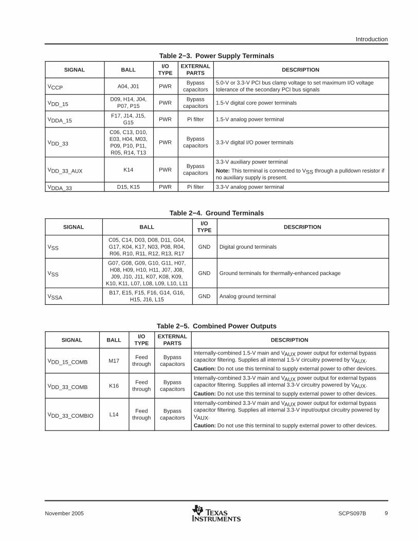
Table 2−3. Power Supply Terminals
SIGNAL BALLI/O
TYPEEXTERNAL
PARTS DESCRIPTION
VCCP A04, J01 PWRBypass
capacitors5.0-V or 3.3-V PCI bus clamp voltage to set maximum I/O voltagetolerance of the secondary PCI bus signals
VDD_15D09, H14, J04,
P07, P15PWR
Bypasscapacitors
1.5-V digital core power terminals
VDDA_15F17, J14, J15,
G15PWR Pi filter 1.5-V analog power terminal
VDD_33
C06, C13, D10,E03, H04, M03,P09, P10, P11,R05, R14, T13
PWRBypass
capacitors3.3-V digital I/O power terminals
VDD_33_AUX K14 PWRBypass
capacitors
3.3-V auxiliary power terminal
Note: This terminal is connected to VSS through a pulldown resistor ifno auxiliary supply is present.
VDDA_33 D15, K15 PWR Pi filter 3.3-V analog power terminal
Table 2−4. Ground Terminals
SIGNAL BALLI/O
TYPE DESCRIPTION
VSS
C05, C14, D03, D08, D11, G04,G17, K04, K17, N03, P08, R04,R06, R10, R11, R12, R13, R17
GND Digital ground terminals
VSS
G07, G08, G09, G10, G11, H07,H08, H09, H10, H11, J07, J08,J09, J10, J11, K07, K08, K09,
K10, K11, L07, L08, L09, L10, L11
GND Ground terminals for thermally-enhanced package
VSSAB17, E15, F15, F16, G14, G16,
H15, J16, L15GND Analog ground terminal
Table 2−5. Combined Power Outputs
SIGNAL BALLI/O
TYPEEXTERNAL
PARTS DESCRIPTION
VDD_15_COMB M17Feed
throughBypass
capacitors
Internally-combined 1.5-V main and VAUX power output for external bypasscapacitor filtering. Supplies all internal 1.5-V circuitry powered by VAUX.
Caution: Do not use this terminal to supply external power to other devices.
VDD_33_COMB K16Feed
throughBypass
capacitors
Internally-combined 3.3-V main and VAUX power output for external bypasscapacitor filtering. Supplies all internal 3.3-V circuitry powered by VAUX.
Caution: Do not use this terminal to supply external power to other devices.
VDD_33_COMBIO L14Feed
throughBypass
capacitors
Internally-combined 3.3-V main and VAUX power output for external bypasscapacitor filtering. Supplies all internal 3.3-V input/output circuitry powered byVAUX.
Caution: Do not use this terminal to supply external power to other devices.
Introduction
10 November 2005SCPS097B
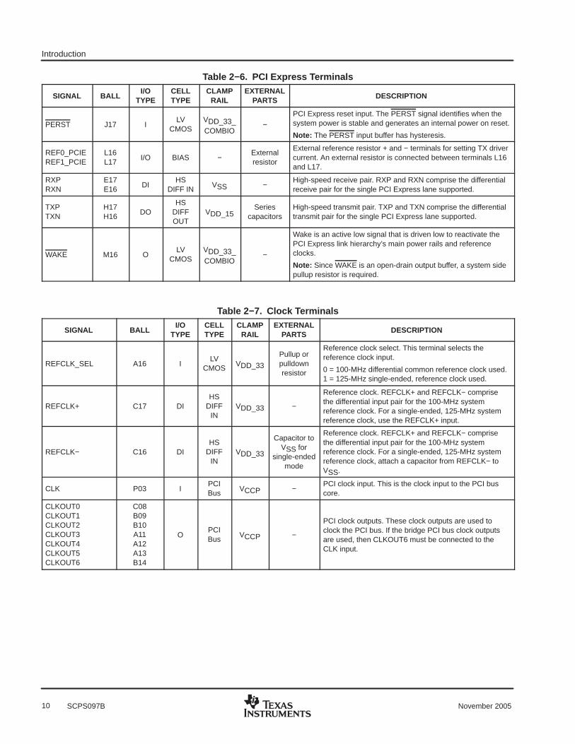
Table 2−6. PCI Express Terminals
SIGNAL BALLI/O
TYPECELLTYPE
CLAMPRAIL
EXTERNALPARTS DESCRIPTION
PERST J17 ILV
CMOSVDD_33_COMBIO
−PCI Express reset input. The PERST signal identifies when thesystem power is stable and generates an internal power on reset.
Note: The PERST input buffer has hysteresis.
REF0_PCIEREF1_PCIE
L16L17
I/O BIAS −Externalresistor
External reference resistor + and − terminals for setting TX drivercurrent. An external resistor is connected between terminals L16and L17.
RXPRXN
E17E16
DIHS
DIFF INVSS −
High-speed receive pair. RXP and RXN comprise the differentialreceive pair for the single PCI Express lane supported.
TXPTXN
H17H16
DOHS
DIFFOUT
VDD_15Series
capacitorsHigh-speed transmit pair. TXP and TXN comprise the differentialtransmit pair for the single PCI Express lane supported.
WAKE M16 OLV
CMOSVDD_33_COMBIO
−
Wake is an active low signal that is driven low to reactivate thePCI Express link hierarchy’s main power rails and referenceclocks.
Note: Since WAKE is an open-drain output buffer, a system sidepullup resistor is required.
Table 2−7. Clock Terminals
SIGNAL BALLI/O
TYPECELLTYPE
CLAMPRAIL
EXTERNALPARTS DESCRIPTION
REFCLK_SEL A16 ILV
CMOSVDD_33
Pullup orpulldownresistor
Reference clock select. This terminal selects thereference clock input.
0 = 100-MHz differential common reference clock used.1 = 125-MHz single-ended, reference clock used.
REFCLK+ C17 DIHS
DIFFIN
VDD_33 −
Reference clock. REFCLK+ and REFCLK− comprisethe differential input pair for the 100-MHz systemreference clock. For a single-ended, 125-MHz systemreference clock, use the REFCLK+ input.
REFCLK− C16 DIHS
DIFFIN
VDD_33
Capacitor toVSS for
single-endedmode
Reference clock. REFCLK+ and REFCLK− comprisethe differential input pair for the 100-MHz systemreference clock. For a single-ended, 125-MHz systemreference clock, attach a capacitor from REFCLK− toVSS.
CLK P03 IPCIBus
VCCP −PCI clock input. This is the clock input to the PCI buscore.
CLKOUT0CLKOUT1CLKOUT2CLKOUT3CLKOUT4CLKOUT5CLKOUT6
C08B09B10A11A12A13B14
OPCIBus
VCCP −
PCI clock outputs. These clock outputs are used toclock the PCI bus. If the bridge PCI bus clock outputsare used, then CLKOUT6 must be connected to theCLK input.
Introduction
11November 2005 SCPS097B
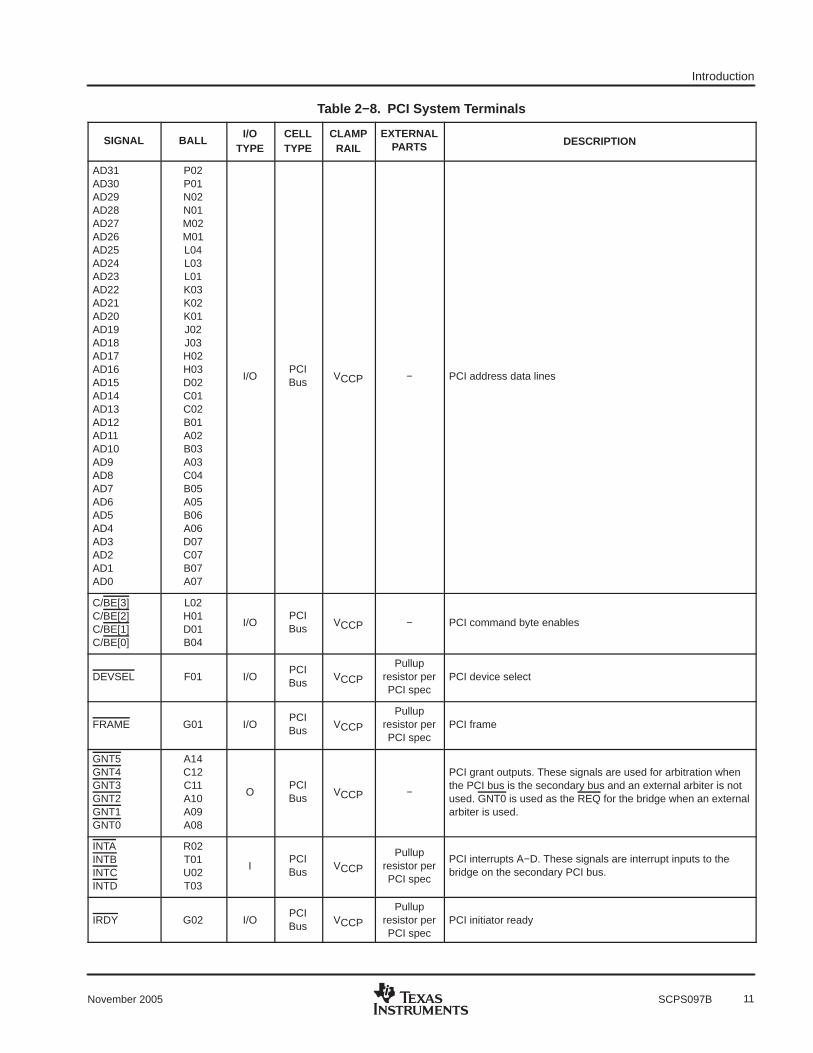
Table 2−8. PCI System Terminals
SIGNAL BALLI/O
TYPECELLTYPE
CLAMPRAIL
EXTERNALPARTS DESCRIPTION
AD31AD30AD29AD28AD27AD26AD25AD24AD23AD22AD21AD20AD19AD18AD17AD16AD15AD14AD13AD12AD11AD10AD9AD8AD7AD6AD5AD4AD3AD2AD1AD0
P02P01N02N01M02M01L04L03L01K03K02K01J02J03H02H03D02C01C02B01A02B03A03C04B05A05B06A06D07C07B07A07
I/OPCIBus
VCCP − PCI address data lines
C/BE[3]C/BE[2]C/BE[1]C/BE[0]
L02H01D01B04
I/OPCIBus
VCCP − PCI command byte enables
DEVSEL F01 I/OPCIBus
VCCP
Pullupresistor perPCI spec
PCI device select
FRAME G01 I/OPCIBus
VCCP
Pullupresistor perPCI spec
PCI frame
GNT5GNT4GNT3GNT2GNT1GNT0
A14C12C11A10A09A08
OPCIBus
VCCP −
PCI grant outputs. These signals are used for arbitration whenthe PCI bus is the secondary bus and an external arbiter is notused. GNT0 is used as the REQ for the bridge when an externalarbiter is used.
INTAINTBINTCINTD
R02T01U02T03
IPCIBus
VCCP
Pullupresistor perPCI spec
PCI interrupts A−D. These signals are interrupt inputs to thebridge on the secondary PCI bus.
IRDY G02 I/OPCIBus
VCCP
Pullupresistor perPCI spec
PCI initiator ready

Introduction
12 November 2005SCPS097B
Table 2−8. PCI System Terminals (Continued)
SIGNAL BALLI/O
TYPECELLTYPE
CLAMPRAIL
EXTERNALPARTS DESCRIPTION
PAR E02 I/OPCIBus
VCCP − PCI bus parity
PERR F03 I/OPCIBus
VCCP
Pullupresistor perPCI spec
PCI parity error
PME M15 ILV
CMOSVDD_33_COMBIO
Pullupresistor perPCI spec
PCI power management event. This terminal may be used todetect PME events from a PCI device on the secondary bus.
Note: The PME input buffer has hysteresis.
REQ5REQ4REQ3REQ2REQ1REQ0
B13B12B11C10C09B08
IPCIBus
VCCP
If unused, aweak pullupresistor perPCI spec
PCI request inputs. These signals are used for arbitration on thesecondary PCI bus when an external arbiter is not used. REQ0is used as the GNT for the bridge when an external arbiter isused.
PRST U03 OPCIBus
VCCP − PCI reset. This terminal is an output to the secondary PCI bus.
SERR E01 I/OPCIBus
VCCP
Pullupresistor perPCI spec
PCI system error
STOP F02 I/OPCIBus
VCCP
Pullupresistor perPCI spec
PCI stop
TRDY G03 I/OPCIBus
VCCP
Pullupresistor perPCI spec
PCI target ready
Table 2−9. Reserved Terminals
SIGNAL BALLI/O
TYPE DESCRIPTION
RSVDN15, N16, P16, R08, T08, T10, T11, T12, T14,T15, T17, U09, U11, U12, U13, U14, U15, U16
O Reserved, do not connect to external signals.
RSVD R16 I Must be connected to VDD_33.
RSVD D16, D17, P17, R09, T09, U10 I Must be connected to VSS.

Introduction
13November 2005 SCPS097B
Table 2−10. Miscellaneous Terminals
SIGNAL BALLI/O
TYPECELLTYPE
CLAMPRAIL
EXTERNALPARTS DESCRIPTION
CLKRUN_EN B15 ILV
CMOSVDD_33
Optionalpullup
resistor
Clock run enable
0 = Clock run support disabled1 = Clock run support enabled
Note: The CLKRUN_EN input buffer has an internal active pulldown.
EXT_ARB_EN A15 ILV
CMOSVDD_33
Optionalpullup
resistor
External arbiter enable
0 = Internal arbiter enabled1 = External arbiter enabled
Note: The EXT_ARB_EN input buffer has an internal active pulldown.
GPIO0 //CLKRUN
T05 I/OLV
CMOSVDD_33
Optionalpullup
resistor
General-purpose I/O 0/clock run. This terminal functions as a GPIOcontrolled by bit 0 (GPIO0_DIR) in the GPIO control register (seeSection 4.59) or the clock run terminal. This terminal is used as clockrun input when the bridge is placed in clock run mode.
Note: In clock run mode, an external pullup resistor is required toprevent the CLKRUN signal from floating.
Note: This terminal has an internal active pullup resistor.
GPIO1 //PWR_OVRD
U05 I/OLV
CMOSVDD_33 −
General-purpose I/O 1/power override. This terminal functions as aGPIO controlled by bit 1 (GPIO1_DIR) in the GPIO control register(see Section 4.59) or the power override output terminal. GPIO1becomes PWR_OVRD when bits 22:20 (POWER_OVRD) in thegeneral control register are set to 001b or 011b (see Section 4.65).
Note: This terminal has an internal active pullup resistor.
GPIO2 T06 I/OLV
CMOSVDD_33 −
General-purpose I/O 2. This terminal functions as a GPIO controlledby bit 2 (GPIO2_DIR) in the GPIO control register (see Section 4.59).
Note: When PERST is deasserted, this terminal must be a 1b toenable the PCI Express 1.0a compatibility mode.
Note: This terminal has an internal active pullup resistor.
GPIO3 U06 I/OLV
CMOSVDD_33 −
General-purpose I/O 3. This terminal functions as a GPIO controlledby bit 3 (GPIO3_DIR) in the GPIO control register (see Section 4.59).
Note: This terminal has an internal active pullup resistor.
GPIO4 // SCL R07 I/OLV
CMOSVDD_33
Optionalpullup
resistor
GPIO4 or serial-bus clock. This terminal functions as serial-bus clockif a pullup resistor is detected on SDA. If a pulldown resistor isdetected on SDA, this terminal functions as GPIO4.
Note: In serial-bus mode, an external pullup resistor is required toprevent the SCL signal from floating.
Note: This terminal has an internal active pullup resistor.
GPIO5 // SDA T07 I/OLV
CMOSVDD_33
Pullup orPulldownresistor
GPIO5 or serial-bus data. This terminal functions as serial-bus data ifa pullup resistor is detected on SDA. If a pulldown resistor is detectedon SDA, this terminal functions as GPIO5.
Note: In serial-bus mode, an external pullup resistor is required toprevent the SDA signal from floating.
GPIO6 U07 I/OLV
CMOSVDD_33 −
General-purpose I/O 6. This terminal functions as a GPIO controlledby bit 6 (GPIO6_DIR) in the GPIO control register (see Section 4.59).
Note: This terminal has an internal active pullup resistor.
GPIO7 U08 I/OLV
CMOSVDD_33 −
General-purpose I/O 7. This terminal functions as a GPIO controlledby bit 7 (GPIO7_DIR) in the GPIO control register (see Section 4.59).
Note: This terminal has an internal active pullup resistor.

Introduction
14 November 2005SCPS097B
Table 2−10. Miscellaneous Terminals (Continued)
SIGNAL BALLI/O
TYPECELLTYPE
CLAMPRAIL
EXTERNALPARTS DESCRIPTION
GRST N17 ILV
CMOSVDD_33_COMBIO
−
Global reset input. Asynchronously resets all logic in device,including sticky bits and power management state machines.
Note: The GRST input buffer has both hysteresis and an internalactive pullup.
LOCK U04 I/OPCIBus
VCCP
Pullupresistor perPCI spec
This terminal functions as PCI LOCK when bit 12 (LOCK_EN) isset in the general control register (see Section 4.65).
Note: In lock mode, an external pullup resistor is required toprevent the LOCK signal from floating.
M66EN R01 IPCIBus
VCCP
Pullupresistor perPCI spec
66-MHz mode enable
0 = Secondary PCI bus and clock outputs operate at 33 MHz1 = Secondary PCI bus and clock outputs operate at 66 MHz
Note: If the PCI bus clock is always 33 MHz, then this terminal isconnected to VSS.
SERIRQ T04 I/OPCIBus
VCCP
Pullup orpulldownresistor
Serial IRQ interface. This terminal functions as a serial IRQinterface if a pullup is detected when PERST is deasserted. If apulldown is detected, then the serial IRQ interface is disabled.
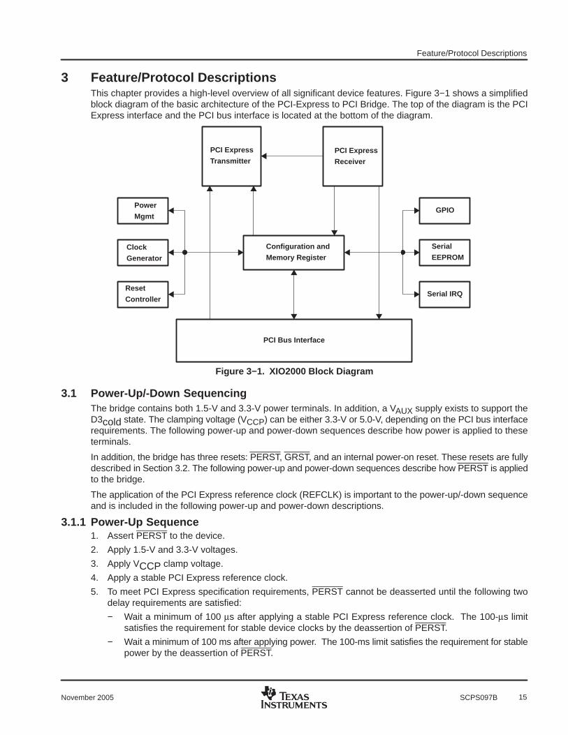
Feature/Protocol Descriptions
15November 2005 SCPS097B
3 Feature/Protocol DescriptionsThis chapter provides a high-level overview of all significant device features. Figure 3−1 shows a simplifiedblock diagram of the basic architecture of the PCI-Express to PCI Bridge. The top of the diagram is the PCIExpress interface and the PCI bus interface is located at the bottom of the diagram.
PCI Express
TransmitterPCI Express
Receiver
PCI Bus Interface
Configuration and
Memory Register
GPIO
Serial
EEPROM
Serial IRQReset
Controller
Clock
Generator
Power
Mgmt
Figure 3−1. XIO2000 Block Diagram
3.1 Power-Up/-Down SequencingThe bridge contains both 1.5-V and 3.3-V power terminals. In addition, a VAUX supply exists to support theD3cold state. The clamping voltage (VCCP) can be either 3.3-V or 5.0-V, depending on the PCI bus interfacerequirements. The following power-up and power-down sequences describe how power is applied to theseterminals.
In addition, the bridge has three resets: PERST, GRST, and an internal power-on reset. These resets are fullydescribed in Section 3.2. The following power-up and power-down sequences describe how PERST is appliedto the bridge.
The application of the PCI Express reference clock (REFCLK) is important to the power-up/-down sequenceand is included in the following power-up and power-down descriptions.
3.1.1 Power-Up Sequence1. Assert PERST to the device.
2. Apply 1.5-V and 3.3-V voltages.
3. Apply VCCP clamp voltage.
4. Apply a stable PCI Express reference clock.
5. To meet PCI Express specification requirements, PERST cannot be deasserted until the following twodelay requirements are satisfied:
− Wait a minimum of 100 µs after applying a stable PCI Express reference clock. The 100-µs limitsatisfies the requirement for stable device clocks by the deassertion of PERST.
− Wait a minimum of 100 ms after applying power. The 100-ms limit satisfies the requirement for stablepower by the deassertion of PERST.
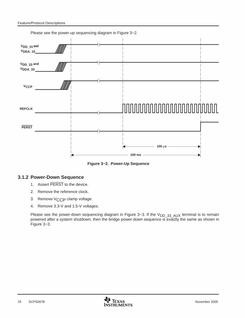
Feature/Protocol Descriptions
16 November 2005SCPS097B
Please see the power-up sequencing diagram in Figure 3−2.
VDD_15 and
VDDA_15
VDD_33 and
VDDA_33
VCCP
REFCLK
PERST
100 ms
100 µs
Figure 3−2. Power-Up Sequence
3.1.2 Power-Down Sequence1. Assert PERST to the device.
2. Remove the reference clock.
3. Remove VCCP clamp voltage.
4. Remove 3.3-V and 1.5-V voltages.
Please see the power-down sequencing diagram in Figure 3−3. If the VDD_33_AUX terminal is to remainpowered after a system shutdown, then the bridge power-down sequence is exactly the same as shown inFigure 3−3.
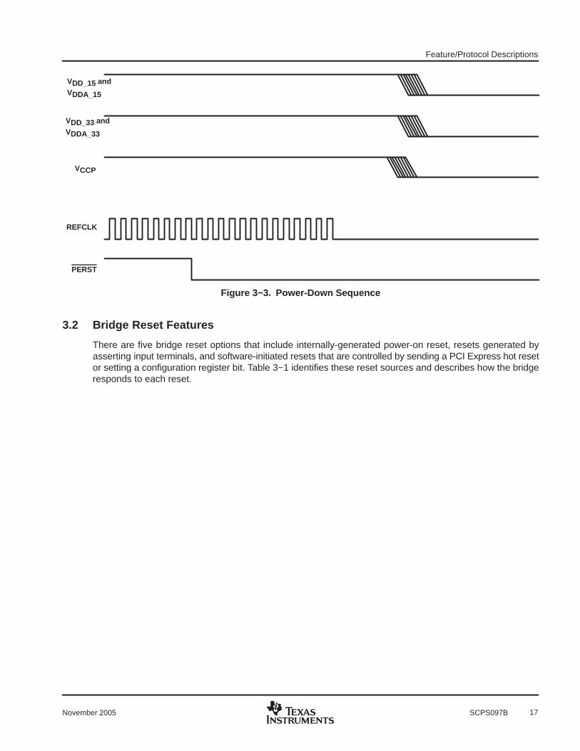
Feature/Protocol Descriptions
17November 2005 SCPS097B
VDD_15 and
VDDA_15
VDD_33 and
VDDA_33
VCCP
REFCLK
PERST
Figure 3−3. Power-Down Sequence
3.2 Bridge Reset Features
There are five bridge reset options that include internally-generated power-on reset, resets generated byasserting input terminals, and software-initiated resets that are controlled by sending a PCI Express hot resetor setting a configuration register bit. Table 3−1 identifies these reset sources and describes how the bridgeresponds to each reset.

Feature/Protocol Descriptions
18 November 2005SCPS097B
Table 3−1. Bridge Reset Options
RESET OPTION XIO2000 FEATURE RESET RESPONSE
Bridgeinternally-generated
power-on reset
During a power-on cycle, the bridge asserts an internalreset and monitors the VDD_15_COMB (M17) terminal.When this terminal reaches 90% of the nominal inputvoltage specification, power is considered stable. Afterstable power, the bridge monitors the PCI Expressreference clock (REFCLK) and waits 10 µs after activeclocks are detected. Then, internal power-on reset isdeasserted.
When the internal power-on reset is asserted, allcontrol registers, state machines, sticky register bits,and power management state machines are initializedto their default state.
In addition, the bridge asserts PCI bus reset (PRST).
Global reset inputGRST (N17)
When GRST is asserted low, an internal power-onreset occurs. This reset is asynchronous and functionsduring both normal power states and VAUX powerstates.
When GRST is asserted low, all control registers, statemachines, sticky register bits, and power managementstate machines are initialized to their default state.
In addition, the bridge asserts PCI bus reset (PRST).
When the rising edge of GRST occurs, the bridgesamples the state of all static control inputs and latchesthe information internally. If an external serial EEPROMis detected, then a download cycle is initiated. Also, theprocess to configure and initialize the PCI Express linkis started. The bridge starts link training within 80 msafter GRST is deasserted.
PCI Express reset inputPERST (J17)
This bridge input terminal is used by an upstream PCIExpress device to generate a PCI Express reset and tosignal a system power good condition.
When PERST is asserted low, the bridge generates aninternal PCI Express reset as defined in the PCIExpress specification.
When PERST transitions from low to high, a systempower good condition is assumed by the bridge.
Note: The system must assert PERST before power isremoved, before REFCLK is removed, or beforeREFCLK becomes unstable.
When PERST is asserted low, all control register bitsthat are not sticky are reset. Within the configurationregister maps, the sticky bits are indicated by the
symbol. Also, all state machines that are notassociated with sticky functionality or VAUX powermanagement are reset.
In addition, the bridge asserts PCI bus reset (PRST).
When the rising edge of PERST occurs, the bridgesamples the state of all static control inputs and latchesthe information internally. If an external serial EEPROMis detected, then a download cycle is initiated. Also, theprocess to configure and initialize the PCI Express linkis started. The bridge starts link training within 80 msafter PERST is deasserted.
PCI Express trainingcontrol hot reset
The bridge responds to a training control hot resetreceived on the PCI Express interface. After a trainingcontrol hot reset, the PCI Express interface enters theDL_DOWN state.
In the DL_DOWN state, all remaining configurationregister bits and state machines are reset. Allremaining bits exclude sticky bits and EEPROMloadable bits. All remaining state machines excludesticky functionality, EEPROM functionality, and VAUXpower management.
Within the configuration register maps, the sticky bitsare indicated by the symbol and the EEPROMloadable bits are indicated by the † symbol.
In addition, the bridge asserts PCI bus reset (PRST).
PCI bus resetPRST (U03)
System software has the ability to assert and deassertthe PRST terminal on the secondary PCI bus interface.This terminal is the PCI bus reset.
When bit 6 (SRST) in the bridge control register atoffset 3Eh (see Section 4.29) is asserted, the bridgeasserts the PRST terminal. A 0 in the SRST bitdeasserts the PRST terminal.
3.3 PCI Express Interface
3.3.1 External Reference Clock
The bridge requires either a differential, 100-MHz common clock reference or a single-ended, 125-MHz clockreference. The selected clock reference must meet all PCI Express Electrical Specification requirements forfrequency tolerance, spread spectrum clocking, and signal electrical characteristics.

Feature/Protocol Descriptions
19November 2005 SCPS097B
If the REFCLK_SEL (A16) input is connected to VSS, then a differential, 100-MHz common clock referenceis expected by the bridge. If the A16 terminal is connected to VDD_33, then a single-ended, 125-MHz clockreference is expected by the bridge.
When the single-ended, 125-MHz clock reference option is enabled, the single-ended clock signal isconnected to the REFCLK+ (C17) terminal. The REFCLK− (C16) terminal is connected to one side of anexternal capacitor with the other side of the capacitor connected to VSS.
When using a single-ended reference clock, care must be taken to ensure interoperability from a system jitterstandpoint. The PCI Express Base Specification does not ensure interoperability when using a differentialreference clock commonly used in PC applications along with a single-ended clock in a noncommon clockarchitecture. System jitter budgets will have to be verified to ensure interoperability. See the PCI Express Jitterand BER White Paper from the PCI-SIG.
3.3.2 Beacon
The bridge supports the PCI Express in-band beacon feature. Beacon is driven on the upstream PCI Expresslink by the bridge to request the reapplication of main power when in the L2 link state. To enable the beaconfeature, bit 10 (BEACON_ENABLE) in the general control register at offset D4h is asserted. See Section 4.65,General Control Register, for details.
If the bridge is in the L2 link state and beacon is enabled, when a secondary PCI bus device asserts PME,then the bridge outputs the beacon signal on the upstream PCI Express link. The beacon signal frequencyis approximately 500 kHz ± 50% with a differential peak-to-peak amplitude of 500 mV and no de-emphasis.Once the beacon is activated, the bridge continues to send the beacon signal until main power is restored asindicated by PERST going inactive. At this time, the beacon signal is deactivated.
3.3.3 Wake
The bridge supports the PCI Express sideband WAKE feature. WAKE is an active low signal driven by thebridge to request the reapplication of main power when in the L2 link state. Since WAKE is an open-collectoroutput, a system-side pullup resistor is required to prevent the signal from floating.
When the bridge is in the L2 link state and PME is received from a device on the secondary PCI bus, the WAKEsignal is asserted low as a wakeup mechanism. Once WAKE is asserted, the bridge drives the signal low untilmain power is restored as indicated by PERST going inactive. At this time, WAKE is deasserted.
3.3.4 Initial Flow Control Credits
The bridge flow control credits are initialized using the rules defined in the PCI Express Base Specification.Table 3−2 identifies the initial flow control credit advertisement for the bridge. The initial advertisement isexactly the same when a second virtual channel (VC) is enabled.
Table 3−2. Initial Flow Control Credit AdvertisementsCREDIT TYPE INITIAL ADVERTISEMENT
Posted request headers (PH) 8
Posted request data (PD) 128
Nonposted header (NPH) 4
Nonposted data (NPD) 4
Completion header (CPLH) 0 (infinite)
Completion data (CPLD) 0 (infinite)
3.3.5 PCI Express Message Transactions
PCI Express messages are both initiated and received by the bridge. Table 3−3 outlines message supportwithin the bridge.
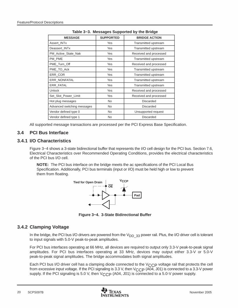
Feature/Protocol Descriptions
20 November 2005SCPS097B
Table 3−3. Messages Supported by the BridgeMESSAGE SUPPORTED BRIDGE ACTION
Assert_INTx Yes Transmitted upstream
Deassert_INTx Yes Transmitted upstream
PM_Active_State_Nak Yes Received and processed
PM_PME Yes Transmitted upstream
PME_Turn_Off Yes Received and processed
PME_TO_Ack Yes Transmitted upstream
ERR_COR Yes Transmitted upstream
ERR_NONFATAL Yes Transmitted upstream
ERR_FATAL Yes Transmitted upstream
Unlock Yes Received and processed
Set_Slot_Power_Limit Yes Received and processed
Hot plug messages No Discarded
Advanced switching messages No Discarded
Vendor defined type 0 No Unsupported request
Vendor defined type 1 No Discarded
All supported message transactions are processed per the PCI Express Base Specification.
3.4 PCI Bus Interface
3.4.1 I/O Characteristics
Figure 3−4 shows a 3-state bidirectional buffer that represents the I/O cell design for the PCI bus. Section 7.6,Electrical Characteristics over Recommended Operating Conditions, provides the electrical characteristicsof the PCI bus I/O cell.
NOTE: The PCI bus interface on the bridge meets the ac specifications of the PCI Local BusSpecification. Additionally, PCI bus terminals (input or I/O) must be held high or low to preventthem from floating.
Tied for Open DrainOE
Pad
VCCP
Figure 3−4. 3-State Bidirectional Buffer
3.4.2 Clamping Voltage
In the bridge, the PCI bus I/O drivers are powered from the VDD_33 power rail. Plus, the I/O driver cell is tolerantto input signals with 5.0-V peak-to-peak amplitudes.
For PCI bus interfaces operating at 66 MHz, all devices are required to output only 3.3-V peak-to-peak signalamplitudes. For PCI bus interfaces operating at 33 MHz, devices may output either 3.3-V or 5.0-Vpeak-to-peak signal amplitudes. The bridge accommodates both signal amplitudes.
Each PCI bus I/O driver cell has a clamping diode connected to the VCCP voltage rail that protects the cellfrom excessive input voltage. If the PCI signaling is 3.3 V, then VCCP (A04, J01) is connected to a 3.3-V powersupply. If the PCI signaling is 5.0 V, then VCCP (A04, J01) is connected to a 5.0-V power supply.

Feature/Protocol Descriptions
21November 2005 SCPS097B
The PCI bus signals attached to the VCCP clamping voltage are identified in the following list:
• In Table 2−7, Clock Terminals, the terminal names include CLK and CLKOUT6:0
• In Table 2−8, PCI System Terminals, all terminal names except for PME
• In Table 2−10, Miscellaneous Terminals, the terminal names include SERIRQ, M66EN, and LOCK
3.4.3 PCI Bus Clock Run
The bridge supports the clock run protocol as specified in the PCI Mobile Design Guide. When the clock runprotocol is enabled, the bridge assumes the role of the central resource master.
To enable the clock run function, terminal B15 (CLKRUN_EN) is asserted high. Then, terminal T05 (GPIO0)is enabled as the CLKRUN signal. An external pullup resistor must be provided to prevent the CLKRUN signalfrom floating. To verify the operational status of the PCI bus clocks, bit 0 (SEC_CLK_STATUS) in the clockrun status register at offset DAh (see Section 4.68) is read.
Since the bridge has several unique features associated with the PCI bus interface, the system designer mustconsider the following interdependencies between these features and the CLKRUN feature:
1. If the system designer chooses to generate the PCI bus clock externally, then the CLKRUN mode of thebridge must be disabled. The central resource function within the bridge only operates as a CLKRUNmaster and does not support the CLKRUN slave mode.
2. If the central resource function has stopped the PCI bus clocks, then the bridge still detects INTx statechanges and will generate and send PCI Express messages upstream.
3. If the serial IRQ interface is enabled and the central resource function has stopped the PCI bus clocks,then any PCI bus device that needs to report an IRQ interrupt asserts CLKRUN to start the bus clocks.
4. When a PCI bus device asserts CLKRUN, the central resource function turns on PCI bus clocks for aminimum of 512 cycles.
5. If the serial IRQ function detects an IRQ interrupt, then the central resource function keeps the PCI busclocks running until the IRQ interrupt is cleared by software.
6. If the central resource function has stopped the PCI bus clocks and the bridge receives a downstreamtransaction that is forwarded to the PCI bus interface, then the bridge asserts CLKRUN to start the busclocks.
7. The central resource function is reset by PCI bus reset (PRST) assuring that clocks are present duringPCI bus resets.
3.4.4 PCI Bus External Arbiter
The bridge supports an external arbiter for the PCI bus. Terminal A15 (EXT_ARB_EN), when asserted high,enables the use of an external arbiter.
When an external arbiter is enabled, GNT0 is connected to the external arbiter as the REQ for the bridge.Likewise, REQ0 is connected to the external arbiter as the GNT for the bridge.
All internal port arbitration features are disabled when an external arbiter is enabled. 128-phase, weightedround-robin (WRR) time-based arbitration, bus parking, arbiter time-out, tier select, and request maskingmodes have no effect if an external arbiter is enabled.

Feature/Protocol Descriptions
22 November 2005SCPS097B
3.4.5 MSI Messages Generated from the Serial IRQ InterfaceWhen properly configured, the bridge converts PCI bus serial IRQ interrupts into PCI Express messagesignaled interrupts (MSI). Classic PCI configuration register space is provided to enable this feature. Thefollowing list identifies the involved configuration registers:
1. Command register at offset 04h, bit 2 (MASTER_ENB) is asserted (see Section 4.3).
2. MSI message control register at offset 62h, bits 0 (MSI_EN) and 6:4 (MM_EN) enable single and multipleMSI messages, respectively (see Section 4.38).
3. MSI message address register at offsets 64h and 68h specifies the message memory address. A nonzeroaddress value in offset 68h initiates 64-bit addressing (see Section 4.40).
4. MSI message data register at offset 6Ch specifies the system interrupt message (see Section 4.41).
5. Serial IRQ mode control register at offset E0h specifies the serial IRQ bus format (see Section 4.72).
6. Serial IRQ edge control register at offset E2h selects either level or edge mode interrupts (seeSection 4.73).
7. Serial IRQ status register at offset E4h reports level mode interrupt status (see Section 4.74).
A PCI Express MSI is generated based on the settings in the serial IRQ edge control register. If the systemis configured for edge mode, then an MSI message is sent when the corresponding serial IRQ interfacesample phase transitions from low to high. If the system is configured for level mode, then an MSI messageis sent when the corresponding IRQ status bit in the serial IRQ status register changes from low to high.
The bridge has a dedicated SERIRQ terminal (T04) for all PCI bus devices that support serialized interrupts.This SERIRQ interface is synchronous to the PCI bus clock input (CLK) frequency. The bridge alwaysgenerates a 17-phase serial IRQ stream. Internally, the bridge detects only 16 IRQ interrupts, IRQ0 framethrough IRQ15 frame. The IOCHCK frame is not monitored by the serial IRQ state machine and nevergenerates an IRQ interrupt or MSI message.
The multiple message enable (MM_EN) field determines the number of unique MSI messages that are sentupstream on the PCI Express link. From 1 message to 16 messages, in powers of 2, are selectable. If fewerthan 16 messages are selected, then the mapping from IRQ interrupts to MSI messages is aliased. Table 3−4illustrates the IRQ interrupt to MSI message mapping based on the number of enabling messages.
Table 3−4. IRQ Interrupt to MSI Message Mapping
IRQ INTERRUPT1 MESSAGEENABLED
2 MESSAGESENABLED
4 MESSAGESENABLED
8 MESSAGESENABLED
16 MESSAGESENABLED
IRQ0 MSI MSG #0 MSI MSG #0 MSI MSG #0 MSI MSG #0 MSI MSG #0
IRQ1 MSI MSG #0 MSI MSG #1 MSI MSG #1 MSI MSG #1 MSI MSG #1
IRQ2 MSI MSG #0 MSI MSG #0 MSI MSG #2 MSI MSG #2 MSI MSG #2
IRQ3 MSI MSG #0 MSI MSG #1 MSI MSG #3 MSI MSG #3 MSI MSG #3
IRQ4 MSI MSG #0 MSI MSG #0 MSI MSG #0 MSI MSG #4 MSI MSG #4
IRQ5 MSI MSG #0 MSI MSG #1 MSI MSG #1 MSI MSG #5 MSI MSG #5
IRQ6 MSI MSG #0 MSI MSG #0 MSI MSG #2 MSI MSG #6 MSI MSG #6
IRQ7 MSI MSG #0 MSI MSG #1 MSI MSG #3 MSI MSG #7 MSI MSG #7
IRQ8 MSI MSG #0 MSI MSG #0 MSI MSG #0 MSI MSG #0 MSI MSG #8
IRQ9 MSI MSG #0 MSI MSG #1 MSI MSG #1 MSI MSG #1 MSI MSG #9
IRQ10 MSI MSG #0 MSI MSG #0 MSI MSG #2 MSI MSG #2 MSI MSG #10
IRQ11 MSI MSG #0 MSI MSG #1 MSI MSG #3 MSI MSG #3 MSI MSG #11
IRQ12 MSI MSG #0 MSI MSG #0 MSI MSG #0 MSI MSG #4 MSI MSG #12
IRQ13 MSI MSG #0 MSI MSG #1 MSI MSG #1 MSI MSG #5 MSI MSG #13
IRQ14 MSI MSG #0 MSI MSG #0 MSI MSG #2 MSI MSG #6 MSI MSG #14
IRQ15 MSI MSG #0 MSI MSG #1 MSI MSG #3 MSI MSG #7 MSI MSG #15
Feature/Protocol Descriptions
23November 2005 SCPS097B
The MSI message format is compatible with the PCI Express request header format for 32-bit and 64-bitmemory write transactions. The system message and message number fields are included in bytes 0 and 1of the data payload.
3.4.6 PCI Bus ClocksThe bridge has seven PCI bus clock outputs and one PCI bus clock input. Up to six PCI bus devices aresupported by the bridge.
Terminal R01 (M66EN) selects the operating frequency of the PCI bus clock outputs. When this input isasserted high, the PCI bus clocks operate at 66 MHz. When this input is deasserted low, the PCI bus clocksoperate at 33 MHz. The clock control register at offset D8h provides 7 control bits to individually enable ordisable each PCI bus clock output (see Section 4.66). The register default is enabled for all 7 outputs.
The PCI bus clock (CLK) input provides the clock to the internal PCI bus core and serial IRQ core. When theinternal PCI bus clock source is selected, PCI bus clock output 6 (CLKOUT6) is connected to the PCI bus clockinput (CLK). When an external PCI bus clock source is selected, the external clock source is connected to thePCI bus clock input (CLK). For external clock mode, all seven CLKOUT6:0 terminals must be disabled usingthe clock control register at offset D8h (see Section 4.66).
3.5 Quality of Service and Isochronous FeaturesThe bridge has both standard and advanced features that provide a robust solution for quality-of-service (QoS)and isochronous applications. These features are best described by divided them into the following threecategories:
• PCI port arbitration. PCI port arbitration determines which bus master is granted the next transaction cycleon the PCI bus. The three PCI port arbitration options are the classic PCI arbiter, the 128-phase, WRRtime-based arbiter, and the 128-phase, WRR aggressive time-based arbiter. The power-up registerdefault is the classic PCI arbiter. The advanced time-based arbiter features are provided to supportisochronous applications.
• PCI isochronous windows. There are four separate windows that allow PCI bus-initiated memorytransactions to be labeled with a PCI Express traffic class (TC) beyond the default TC0. Each windowdesignates a range of PCI memory space that is mapped to a specified TC label. The power-up registerdefault is all four windows disabled.
• PCI Express extended VC with VC arbitration. With an extended VC, system software can map a particularTC to a specific VC. The differentiated traffic on the second VC then uses dedicated system resourcesto support a QoS environment. VC arbitration is provided to gate traffic to the upstream PCI Express link.The three VC arbitration options include strict priority, hardware-fixed round-robin, and 32-phase WRR.The power-up register default is strict priority with the second VC disabled.
When configuring these standard and advanced features, the following rules must be followed:
1. The default mode is classic PCI arbiter with the PCI isochronous windows disabled and the second VCdisabled. The bridge performs default PCI bus arbitration without any arbiter-related configuration registersetup.
2. If a second VC is enabled, then at least one PCI isochronous window must be configured to map upstreamtransactions to the second VC.
3. If a second VC is enabled, then any VC arbiter option interacts with any PCI port arbiter option.
4. To enable the PCI isochronous windows it is not required to enable a second VC. The memory space totraffic mapping always uses VC0 for all upstream traffic.
5. When programming the upstream isochronous window base and limit registers, the 32-bit base/limitaddress must be DWORD aligned and the limit address must be greater than the base address.
The following sections describe in detail the standard and advanced bridge features for QoS and isochronousapplications.

Feature/Protocol Descriptions
24 November 2005SCPS097B
3.5.1 PCI Port Arbitration
The internal PCI port arbitration logic supports up to six external PCI bus devices plus the bridge. Three optionsexist when configuring the bridge arbiter for these seven bus devices: classic PCI arbiter, 128-phase, WRRtime-based arbiter, and 128-phase, WRR aggressive time-based arbiter.
3.5.1.1 Classic PCI Arbiter
The classic PCI arbiter is configured through the classic PCI configuration space at offset DCh. Table 3−5identifies and describes the registers associated with classic PCI arbitration mode.
Table 3−5. Classic PCI Arbiter RegistersPCI OFFSET REGISTER NAME DESCRIPTION
Classic PCI configurationregister DCh
Arbiter control (see Section 4.69)
Contains a two-tier priority scheme for the bridge and six PCI bus devices. The bridgedefaults to the high priority tier. The six PCI bus devices default to the low priority tier. Abus parking control bit (bit 7, PARK) is provided.
Classic PCI configurationregister DDh
Arbiter request mask (see Section 4.70)
Six mask bits provide individual control to block each PCI Bus REQ input. Bit 7(ARB_TIMEOUT) in the arbiter request mask register enables generating timeoutstatus if a PCI device does not respond within 16 PCI bus clocks. Bit 6 (AUTO_MASK)in the arbiter request mask register automatically masks a PCI bus REQ if the devicedoes not respond after GNT is issued. The AUTO_MASK bit is cleared to disable anyautomatically generated mask.
Classic PCI configurationregister DEh
Arbiter time-out status(see Section 4.71)
When bit 7 (ARB_TIMEOUT) in the arbiter request mask register (see Section 4.70) isasserted, timeout status for each PCI bus device is reported in this register.
3.5.1.2 128-Phase, WRR Time-Based Arbiter
The 128-phase, WRR time-based arbiter is configured through the PCI express VC extended configurationspace at offset 150h and the device control memory window register map.
The 128-phase, WRR time-based arbiter periodically asserts GNT to a PCI master device based on entrieswithin a port arbitration table. There are actually two port arbitration tables within the bridge. The first tableis accessed through the PCI Express VC extended configuration register space using configuration read/writetransactions. The second table is internal and is used by the PCI bus arbiter to make GNT decisions. Aconfiguration register load function exists to transfer the contents of the configuration register table to theinternal table.
The port arbitration table uses a 4-bit field to identify the secondary bus master that receives GNT during eachphase of the time-based WRR arbitration. For the arbiter to recognize a bus master REQ and to generate GNT,software must allocate at least three consecutive phases to the same port number.
Table 3−6 defines the mapping relationship of the PCI bus devices to a port number in the port arbitration table.
Table 3−6. Port Number to PCI Bus Device Mapping
PORT NUMBER GNT PCI DEVICE
0000b Internal GNT for PCI master state machine Internal REQ from PCI master state machine
0001b External GNT0 External REQ0
0010b External GNT1 External REQ1
0011b External GNT2 External REQ2
0100b External GNT3 External REQ3
0101b External GNT4 External REQ4
0110b External GNT5 External REQ5
0111b−1111b Reserved −
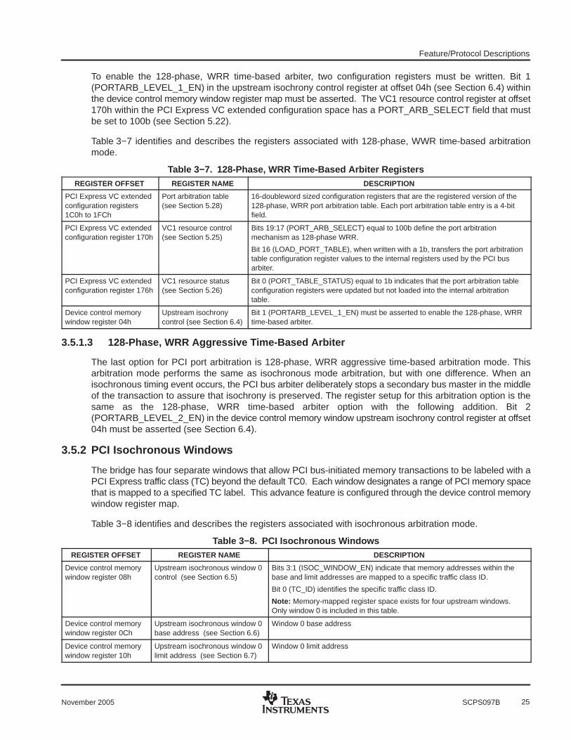
Feature/Protocol Descriptions
25November 2005 SCPS097B
To enable the 128-phase, WRR time-based arbiter, two configuration registers must be written. Bit 1(PORTARB_LEVEL_1_EN) in the upstream isochrony control register at offset 04h (see Section 6.4) withinthe device control memory window register map must be asserted. The VC1 resource control register at offset170h within the PCI Express VC extended configuration space has a PORT_ARB_SELECT field that mustbe set to 100b (see Section 5.22).
Table 3−7 identifies and describes the registers associated with 128-phase, WWR time-based arbitrationmode.
Table 3−7. 128-Phase, WRR Time-Based Arbiter RegistersREGISTER OFFSET REGISTER NAME DESCRIPTION
PCI Express VC extendedconfiguration registers1C0h to 1FCh
Port arbitration table(see Section 5.28)
16-doubleword sized configuration registers that are the registered version of the128-phase, WRR port arbitration table. Each port arbitration table entry is a 4-bitfield.
PCI Express VC extendedconfiguration register 170h
VC1 resource control(see Section 5.25)
Bits 19:17 (PORT_ARB_SELECT) equal to 100b define the port arbitrationmechanism as 128-phase WRR.
Bit 16 (LOAD_PORT_TABLE), when written with a 1b, transfers the port arbitrationtable configuration register values to the internal registers used by the PCI busarbiter.
PCI Express VC extendedconfiguration register 176h
VC1 resource status(see Section 5.26)
Bit 0 (PORT_TABLE_STATUS) equal to 1b indicates that the port arbitration tableconfiguration registers were updated but not loaded into the internal arbitrationtable.
Device control memorywindow register 04h
Upstream isochronycontrol (see Section 6.4)
Bit 1 (PORTARB_LEVEL_1_EN) must be asserted to enable the 128-phase, WRRtime-based arbiter.
3.5.1.3 128-Phase, WRR Aggressive Time-Based Arbiter
The last option for PCI port arbitration is 128-phase, WRR aggressive time-based arbitration mode. Thisarbitration mode performs the same as isochronous mode arbitration, but with one difference. When anisochronous timing event occurs, the PCI bus arbiter deliberately stops a secondary bus master in the middleof the transaction to assure that isochrony is preserved. The register setup for this arbitration option is thesame as the 128-phase, WRR time-based arbiter option with the following addition. Bit 2(PORTARB_LEVEL_2_EN) in the device control memory window upstream isochrony control register at offset04h must be asserted (see Section 6.4).
3.5.2 PCI Isochronous Windows
The bridge has four separate windows that allow PCI bus-initiated memory transactions to be labeled with aPCI Express traffic class (TC) beyond the default TC0. Each window designates a range of PCI memory spacethat is mapped to a specified TC label. This advance feature is configured through the device control memorywindow register map.
Table 3−8 identifies and describes the registers associated with isochronous arbitration mode.
Table 3−8. PCI Isochronous WindowsREGISTER OFFSET REGISTER NAME DESCRIPTION
Device control memorywindow register 08h
Upstream isochronous window 0control (see Section 6.5)
Bits 3:1 (ISOC_WINDOW_EN) indicate that memory addresses within thebase and limit addresses are mapped to a specific traffic class ID.
Bit 0 (TC_ID) identifies the specific traffic class ID.
Note: Memory-mapped register space exists for four upstream windows.Only window 0 is included in this table.
Device control memorywindow register 0Ch
Upstream isochronous window 0base address (see Section 6.6)
Window 0 base address
Device control memorywindow register 10h
Upstream isochronous window 0limit address (see Section 6.7)
Window 0 limit address

Feature/Protocol Descriptions
26 November 2005SCPS097B
3.5.3 PCI Express Extended VC With VC Arbitration
When a second VC is enabled, the bridge has three arbitration options that determine which VC is grantedaccess to the upstream PCI Express link. These three arbitration modes include strict priority, hardware-fixedround-robin, and 32-phase WRR. The default mode is strict priority. For all three arbitration modes, if thesecond VC is disabled, then VC0 is always granted.
To map upstream transactions to the extended VC, the following registers must be programmed:
1. Bit 0 (ISOC_ENABLE) is asserted in the upstream isochrony control register at device control memorywindow register offset 04h (see Section 6.4).
2. At least one PCI isochronous window register set must be programmed. Please see Section 3.5.2 for adescription on how to program this advanced feature.
3. The traffic class ID selected for the PCI isochronous window(s) must be assigned to the extended VC.This is accomplished by asserting the corresponding bit in the TC_VC_MAP field in the VC resourcecontrol register (VC1) at PCI Express extended register offset 170h (see Section 5.25).
4. The extended VC must be enabled. This is accomplished by asserting bit 31 (VC_EN) and programmingbits 26:24 (VC_ID) in the VC resource control register (VC1) at PCI Express extended register offset 170h.
3.5.3.1 Strict Priority Arbitration Mode
Strict priority arbitration always grants VC1 traffic over VC0 traffic. If the traffic on VC1 uses 100% of theupstream link bandwidth, then VC0 traffic is blocked. This mode is enabled when bit 25(STRICT_PRIORITY_EN) in the general control register at offset D4h equals 1b (see Section 4.65).
For applications that require QoS or isochronous operation, this arbitration mode is recommended. In thismode, all traffic on VC1 is assured access to the upstream link and VC0 traffic is best effort with a lower priority.
3.5.3.2 Hardware-Fixed, Round-Robin Arbitration
Hardware-fixed, round-robin arbitration alternates between VC0 and the second VC. Over an extended periodof time, if both VCs are heavily loaded with equal data payloads, each VC is granted approximately 50% ofthe upstream link bandwidth. The PCI configuration registers described in Table 3−9 configure thehardware-fixed, round-robin arbitration mode.
Table 3−9. Hardware-Fixed, Round-Robin Arbiter RegistersPCI OFFSET REGISTER NAME DESCRIPTION
Classic PCI configurationregister D4h
General control (see Section 4.65)
Bit 25 (STRICT_PRIORITY_EN) equal to 0b enables either hardware-fixed,round-robin or 32-phase, WRR arbitration mode.
Classic PCI configurationregister 15Ch
Port VC control (see Section 5.19)
Bits 3:1 (VC_ARB_SELECT) equal to 000b enables hardware-fixed,round-robin arbitration mode.
3.5.3.3 32-Phase, WRR Arbitration Mode
When the second upstream VC is enabled, the VC arbiter selects the next PCI Express upstream linktransaction based on entries within a VC arbitration table. There are actually two VC arbitration tables withinthe bridge. The first table is accessed through the extended PCI Express configuration register space usingconfiguration read/write transactions. The second table is internal and is used by the VC arbiter to makeselection decisions. A configuration register load function exists to transfer the contents of the configurationregister table to the internal table.
The VC arbitration table uses a 4-bit field to identify the VC that is selected during each arbiter cycle. Bits 2:0of this 4-bit field are loaded with the VC_ID assigned to each VC. For the arbiter to recognize a VC request,the software must allocate only 1 phase to the same VC_ID.
The PCI configuration registers described in Table 3−10 configure the 32-phase, WRR arbitration mode.
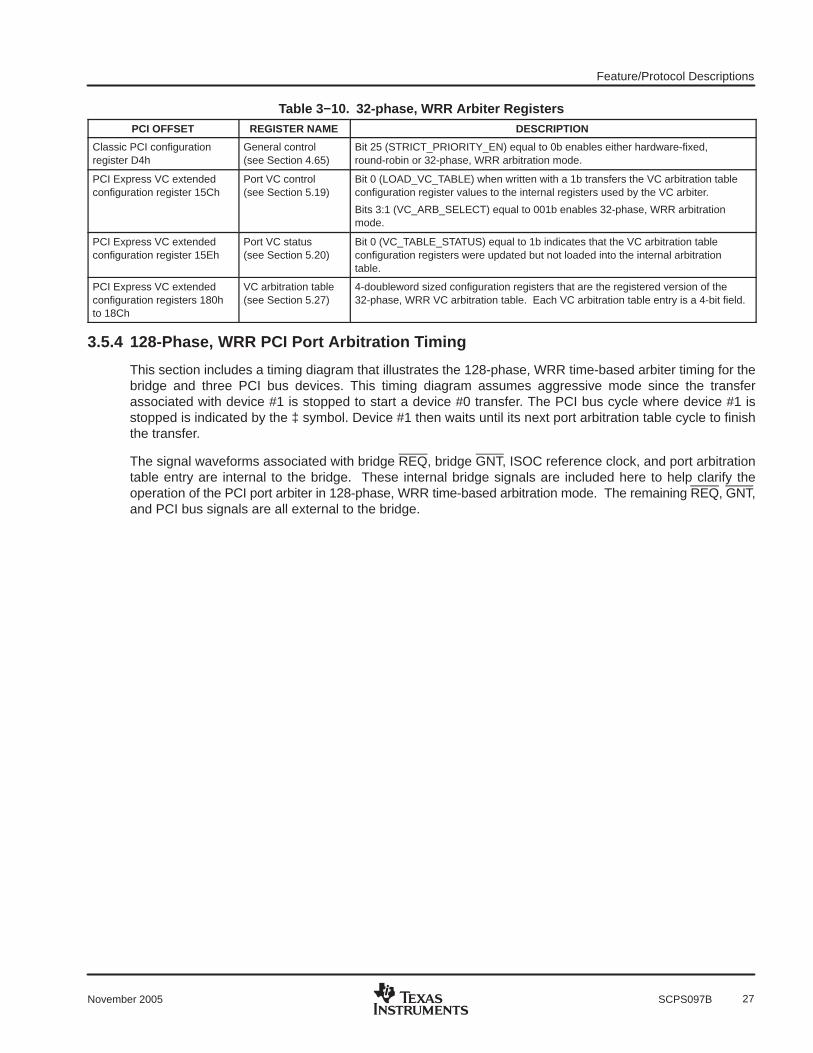
Feature/Protocol Descriptions
27November 2005 SCPS097B
Table 3−10. 32-phase, WRR Arbiter RegistersPCI OFFSET REGISTER NAME DESCRIPTION
Classic PCI configurationregister D4h
General control (see Section 4.65)
Bit 25 (STRICT_PRIORITY_EN) equal to 0b enables either hardware-fixed,round-robin or 32-phase, WRR arbitration mode.
PCI Express VC extendedconfiguration register 15Ch
Port VC control (see Section 5.19)
Bit 0 (LOAD_VC_TABLE) when written with a 1b transfers the VC arbitration tableconfiguration register values to the internal registers used by the VC arbiter.
Bits 3:1 (VC_ARB_SELECT) equal to 001b enables 32-phase, WRR arbitrationmode.
PCI Express VC extendedconfiguration register 15Eh
Port VC status (see Section 5.20)
Bit 0 (VC_TABLE_STATUS) equal to 1b indicates that the VC arbitration tableconfiguration registers were updated but not loaded into the internal arbitrationtable.
PCI Express VC extendedconfiguration registers 180hto 18Ch
VC arbitration table(see Section 5.27)
4-doubleword sized configuration registers that are the registered version of the32-phase, WRR VC arbitration table. Each VC arbitration table entry is a 4-bit field.
3.5.4 128-Phase, WRR PCI Port Arbitration Timing
This section includes a timing diagram that illustrates the 128-phase, WRR time-based arbiter timing for thebridge and three PCI bus devices. This timing diagram assumes aggressive mode since the transferassociated with device #1 is stopped to start a device #0 transfer. The PCI bus cycle where device #1 isstopped is indicated by the ‡ symbol. Device #1 then waits until its next port arbitration table cycle to finishthe transfer.
The signal waveforms associated with bridge REQ, bridge GNT, ISOC reference clock, and port arbitrationtable entry are internal to the bridge. These internal bridge signals are included here to help clarify theoperation of the PCI port arbiter in 128-phase, WRR time-based arbitration mode. The remaining REQ, GNT,and PCI bus signals are all external to the bridge.
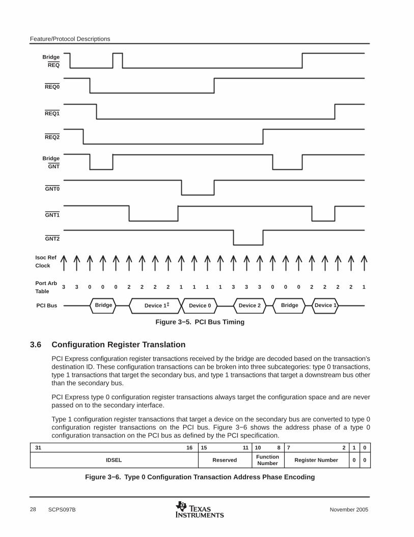
Feature/Protocol Descriptions
28 November 2005SCPS097B
Bridge
REQ
REQ0
REQ1
REQ2
Bridge
GNT
GNT0
GNT1
GNT2
Isoc Ref
Clock
Port Arb
Table
PCI Bus
3 3 0 0 0 2 2 2 2 1 1 1 1 3 3 3 0 0 0 2 2 2 2 1
Bridge Device 1 ‡ Device 0 Device 2 Bridge Device 1
Figure 3−5. PCI Bus Timing
3.6 Configuration Register Translation
PCI Express configuration register transactions received by the bridge are decoded based on the transaction’sdestination ID. These configuration transactions can be broken into three subcategories: type 0 transactions,type 1 transactions that target the secondary bus, and type 1 transactions that target a downstream bus otherthan the secondary bus.
PCI Express type 0 configuration register transactions always target the configuration space and are neverpassed on to the secondary interface.
Type 1 configuration register transactions that target a device on the secondary bus are converted to type 0configuration register transactions on the PCI bus. Figure 3−6 shows the address phase of a type 0configuration transaction on the PCI bus as defined by the PCI specification.
31 16 15 11 10 8 7 2 1 0
IDSEL ReservedFunctionNumber Register Number 0 0
Figure 3−6. Type 0 Configuration Transaction Address Phase Encoding

Feature/Protocol Descriptions
29November 2005 SCPS097B
In addition, the bridge converts the destination ID device number to one of the AD[31:16] lines as the IDSELsignal. The implemented IDSEL signal mapping is shown in Table 3−11.
Table 3−11. Type 0 Configuration Transaction IDSEL Mapping
DEVICENUMBER
AD[31:16]
00000 0000 0000 0000 0001
00001 0000 0000 0000 0010
00010 0000 0000 0000 0100
00011 0000 0000 0000 1000
00100 0000 0000 0001 0000
00101 0000 0000 0010 0000
00110 0000 0000 0100 0000
00111 0000 0000 1000 0000
01000 0000 0001 0000 0000
01001 0000 0010 0000 0000
01010 0000 0100 0000 0000
01011 0000 1000 0000 0000
01100 0001 0000 0000 0000
01101 0010 0000 0000 0000
01110 0100 0000 0000 0000
01111 1000 0000 0000 0000
1xxxx 0000 0000 0000 0000
Type 1 configuration registers transactions that target a downstream bus other then the secondary bus areoutput on the PCI bus as type 1 PCI configuration transactions. Figure 3−7 shows the address phase of a type1 configuration transaction on the PCI bus as defined by the PCI specification.
31 24 23 16 15 11 10 8 7 2 1 0
Reserved Bus Number Device NumberFunctionNumber Register Number 0 1
Figure 3−7. Type 1 Configuration Transaction Address Phase Encoding
3.7 PCI Interrupt Conversion to PCI Express Messages
The bridge converts interrupts from the PCI bus sideband interrupt signals to PCI Express interrupt messages.
PCI Express Assert_INTx messages are generated when one of the PCI bus INT[A:D] input terminalstransitions low. The requester ID portion of the Assert_INTx message uses the value stored in the primary busnumber register (see Section 4.11) as the bus number, 0 as the device number, and 0 as the function number.The tag field for each Assert_INTx message is 00h. The lower two bits in the code field indicate the assertedinterrupt signal.
PCI Express Deassert_INTx messages are generated when one of the PCI bus INT[A:D] input terminalstransitions high. The requester ID portion of the Deassert_INTx message uses the value stored in the primarybus number register as the bus number, 0 as the device number, and 0 as the function number. The Tag fieldfor each Deassert_INTx message is 00h. The lower two bits in the code field indicate the deasserted interruptsignal.
Table 3−12, Figure 3−8, and Figure 3−9 illustrate the format for both the assert and deassert INTx messages.

Feature/Protocol Descriptions
30 November 2005SCPS097B
Table 3−12. Interrupt Mapping In The Code Field
INTERRUPT CODE FIELD
INTA 00
INTB 01
INTC 10
INTD 11
+0 +1 +2 +3
7 6 5 4 3 2 1 0 7 6 5 4 3 2 1 0 7 6 5 4 3 2 1 0 7 6 5 4 3 2 1 0
Byte 0> RFmt Type
RTC
ReservedT E Attr
RLength
Byte 0> R0 1 1 0 1 0 0
R0 0 0
ReservedD P 0 0
R0 0 0 0 0 0 0 0 0 0
Byte 4> Requester ID TagCode
Byte 4> Requester ID Tag0 0 1 0 0 0 x x
Byte 8>ReservedByte 12> Reserved
Figure 3−8. PCI Express ASSERT_INTX Message
+0 +1 +2 +3
7 6 5 4 3 2 1 0 7 6 5 4 3 2 1 0 7 6 5 4 3 2 1 0 7 6 5 4 3 2 1 0
Byte 0> RFmt Type
RTC
ReservedT E Attr
RLength
Byte 0> R0 1 1 0 1 0 0
R0 0 0
ReservedD P 0 0
R0 0 0 0 0 0 0 0 0 0
Byte 4> Requester ID TagCode
Byte 4> Requester ID Tag0 0 1 0 0 1 x x
Byte 8>ReservedByte 12> Reserved
Figure 3−9. PCI Express DEASSERT_INTX Message
3.8 PME Conversion to PCI Express Messages
When the PCI bus PME input transitions low, the bridge generates and sends a PCI Express PME messageupstream. The requester ID portion of the PME message uses the stored value in the secondary bus numberregister as the bus number, 0 as the device number, and 0 as the function number. The Tag field for each PMEmessage is 00h. A PME message is sent periodically until the PME signal transitions high.
Figure 3−10 illustrates the format for a PCI Express PME message.
+0 +1 +2 +3
7 6 5 4 3 2 1 0 7 6 5 4 3 2 1 0 7 6 5 4 3 2 1 0 7 6 5 4 3 2 1 0
Byte 0> RFmt Type
RTC
ReservedT E Attr
RLength
Byte 0> R0 1 1 0 0 0 0
R0 0 0
ReservedD P 0 0
R0 0 0 0 0 0 0 0 0 0
Byte 4> Requester ID TagCode
Byte 4> Requester ID Tag0 0 0 1 1 0 0 0
Byte 8>ReservedByte 12> Reserved
Figure 3−10. PCI Express PME Message

Feature/Protocol Descriptions
31November 2005 SCPS097B
3.9 PCI Express To PCI Bus Lock Conversion
The bus-locking protocol defined in the PCI Express Base Specification and PCI Local Bus Specification isprovided on the bridge as an additional compatibility feature. The PCI bus LOCK signal is a dedicated outputthat is enabled by setting bit 12 in the general control register at offset D4h. See Section 4.65, General ControlRegister, for details.
NOTE: The use of LOCK is only supported by PCI-Express to PCI Bridges in the downstreamdirection (away from the root complex).
PCI Express locked-memory read request transactions are treated the same as PCI Express memory readtransactions except that the bridge returns a completion for a locked-memory read. Also, the bridge uses thePCI LOCK protocol when initiating the memory read transaction on the PCI bus.
When a PCI Express locked-memory read request transaction is received and the bridge is not already locked,the bridge arbitrates for use of the LOCK terminal by asserting REQ. If the bridge receives GNT and the LOCKterminal is high, then the bridge drives the LOCK terminal low after the address phase of the firstlocked-memory read transaction to take ownership of LOCK. The bridge continues to assert LOCK exceptduring the address phase of locked transactions. If the bridge receives GNT and the LOCK terminal is low,then the bridge deasserts its REQ and waits until LOCK is high and the bus is idle before re-arbitrating for theuse of LOCK.
DataAddress
CLK
FRAME
LOCK
AD
IRDY
TRDY
DEVSEL
Figure 3−11. Starting A Locked Sequence
Once the bridge has ownership of LOCK, the bridge initiates the lock read as a memory read transaction onthe PCI bus. When the target of the locked-memory read returns data, the bridge is considered locked andall transactions not associated with the locked sequence are blocked by the bridge.
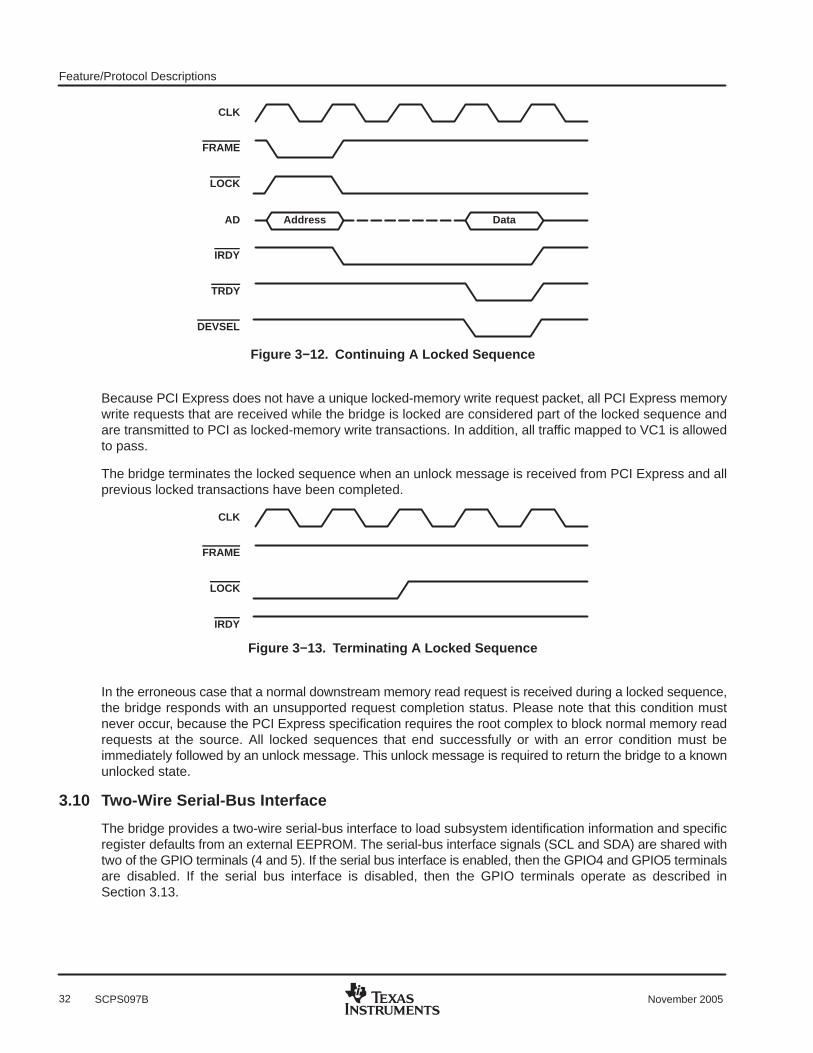
Feature/Protocol Descriptions
32 November 2005SCPS097B
DataAddress
CLK
FRAME
LOCK
AD
IRDY
TRDY
DEVSEL
Figure 3−12. Continuing A Locked Sequence
Because PCI Express does not have a unique locked-memory write request packet, all PCI Express memorywrite requests that are received while the bridge is locked are considered part of the locked sequence andare transmitted to PCI as locked-memory write transactions. In addition, all traffic mapped to VC1 is allowedto pass.
The bridge terminates the locked sequence when an unlock message is received from PCI Express and allprevious locked transactions have been completed.
CLK
FRAME
LOCK
IRDY
Figure 3−13. Terminating A Locked Sequence
In the erroneous case that a normal downstream memory read request is received during a locked sequence,the bridge responds with an unsupported request completion status. Please note that this condition mustnever occur, because the PCI Express specification requires the root complex to block normal memory readrequests at the source. All locked sequences that end successfully or with an error condition must beimmediately followed by an unlock message. This unlock message is required to return the bridge to a knownunlocked state.
3.10 Two-Wire Serial-Bus Interface
The bridge provides a two-wire serial-bus interface to load subsystem identification information and specificregister defaults from an external EEPROM. The serial-bus interface signals (SCL and SDA) are shared withtwo of the GPIO terminals (4 and 5). If the serial bus interface is enabled, then the GPIO4 and GPIO5 terminalsare disabled. If the serial bus interface is disabled, then the GPIO terminals operate as described inSection 3.13.

Feature/Protocol Descriptions
33November 2005 SCPS097B
3.10.1 Serial-Bus Interface Implementation
To enable the serial-bus interface, a pullup resistor must be implemented on the SDA signal. At the rising edgeof PERST or GRST, whichever occurs later in time, the SDA terminal is checked for a pullup resistor. If oneis detected, then bit 3 (SBDETECT) in the serial-bus control and status register (see Section 4.58) is set.Software may disable the serial-bus interface at any time by writing a 0b to the SBDETECT bit. If no externalEEPROM is required, then the serial-bus interface is permanently disabled by attaching a pulldown resistorto the SDA signal.
The bridge implements a two-terminal serial interface with 1 clock signal (SCL) and 1 data signal (SDA). TheSCL signal is a unidirectional output from the bridge and the SDA signal is bidirectional. Both are open-drainsignals and require pullup resistors. The bridge is a bus master device and drives SCL at approximately60 kHz during data transfers and places SCL in a high-impedance state (0 frequency) during bus idle states.The serial EEPROM is a bus slave device and must acknowledge a slave address equal to A0h. Figure 3−14illustrates an example application implementing the two-wire serial bus.
GPIO4 // SCL
GPIO5 // SDA
VDD_33
A0
A1
A2
SCL
SDA
XIO2000
SerialEEPROM
Figure 3−14. Serial EEPROM Application
3.10.2 Serial-Bus Interface Protocol
All data transfers are initiated by the serial-bus master. The beginning of a data transfer is indicated by a startcondition, which is signaled when the SDA line transitions to the low state while SCL is in the high state, asillustrated in Figure 3−15. The end of a requested data transfer is indicated by a stop condition, which issignaled by a low-to-high transition of SDA while SCL is in the high state, as shown in Figure 3−15. Data onSDA must remain stable during the high state of the SCL signal, as changes on the SDA signal during the highstate of SCL are interpreted as control signals, that is, a start or stop condition.

Feature/Protocol Descriptions
34 November 2005SCPS097B
SDA
SCL
StartCondition
StopCondition
Change ofData Allowed
Data Line Stable,Data Valid
Figure 3−15. Serial-Bus Start/Stop Conditions and Bit Transfers
Data is transferred serially in 8-bit bytes. During a data transfer operation, the exact number of bytes that aretransmitted is unlimited. However, each byte must be followed by an acknowledge bit to continue the datatransfer operation. An acknowledge (ACK) is indicated by the data byte receiver pulling the SDA signal low,so that it remains low during the high state of the SCL signal. Figure 3−16 illustrates the acknowledge protocol.
SCL FromMaster 1 2 3 7 8 9
SDA Output By Transmitter
SDA OutputBy Receiver
Figure 3−16. Serial-Bus Protocol Acknowledge
The bridge performs three basic serial-bus operations: single byte reads, single byte writes, and multibytereads. The single byte operations occur under software control. The multibyte read operations are performedby the serial EEPROM initialization circuitry immediately after a PCI Express reset. See Section 3.10.3,Serial-Bus EEPROM Application, for details on how the bridge automatically loads the subsystemidentification and other register defaults from the serial-bus EEPROM.
Figure 3−17 illustrates a single byte write. The bridge issues a start condition and sends the 7-bit slave deviceaddress and the R/W command bit is equal to 0b. A 0b in the R/W command bit indicates that the data transferis a write. The slave device acknowledges if it recognizes the slave address. If no acknowledgment is receivedby the bridge, then bit 1 (SB_ERR) is set in the serial-bus control and status register (PCI offset B3h, seeSection 4.58). Next, the EEPROM word address is sent by the bridge, and another slave acknowledgmentis expected. Then the bridge delivers the data byte MSB first and expects a final acknowledgment beforeissuing the stop condition.
S b6 b4b5 b3 b2 b1 b0 0 b7 b6 b5 b4 b3 b2 b1 b0A A
Slave Address Word Address
R/W
S/P = Start/Stop ConditionA = Slave Acknowledgement
b7 b6 b4b5 b3 b2 b1 b0 A P
Data Byte
Figure 3−17. Serial-Bus Protocol—Byte Write
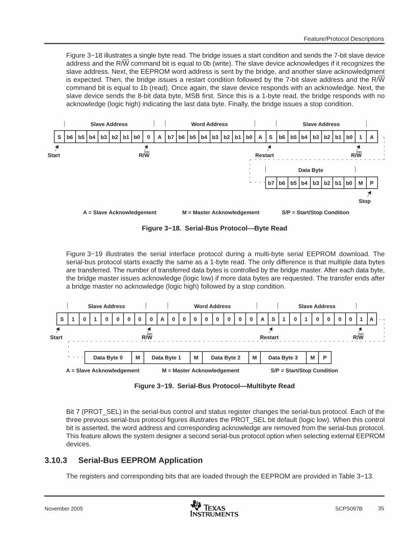
Feature/Protocol Descriptions
35November 2005 SCPS097B
Figure 3−18 illustrates a single byte read. The bridge issues a start condition and sends the 7-bit slave deviceaddress and the R/W command bit is equal to 0b (write). The slave device acknowledges if it recognizes theslave address. Next, the EEPROM word address is sent by the bridge, and another slave acknowledgmentis expected. Then, the bridge issues a restart condition followed by the 7-bit slave address and the R/Wcommand bit is equal to 1b (read). Once again, the slave device responds with an acknowledge. Next, theslave device sends the 8-bit data byte, MSB first. Since this is a 1-byte read, the bridge responds with noacknowledge (logic high) indicating the last data byte. Finally, the bridge issues a stop condition.
S b6 b4b5 b3 b2 b1 b0 0 b7 b6 b5 b4 b3 b2 b1 b0A A
Slave Address Word Address
R/W
S b6 b4b5 b3 b2 b1 b0 1 A
Slave Address
S/P = Start/Stop ConditionM = Master Acknowledgement
b7 b6 b4b5 b3 b2 b1 b0 M P
Data Byte
Start Restart R/W
A = Slave Acknowledgement
Stop
Figure 3−18. Serial-Bus Protocol—Byte Read
Figure 3−19 illustrates the serial interface protocol during a multi-byte serial EEPROM download. Theserial-bus protocol starts exactly the same as a 1-byte read. The only difference is that multiple data bytesare transferred. The number of transferred data bytes is controlled by the bridge master. After each data byte,the bridge master issues acknowledge (logic low) if more data bytes are requested. The transfer ends aftera bridge master no acknowledge (logic high) followed by a stop condition.
S 1 10 0 0 0 0 0 0 0 0 0 0 0 0 0A A
Slave Address Word Address
R/W
Data Byte 1 Data Byte 2 Data Byte 3 M PMM
M = Master Acknowledgement S/P = Start/Stop ConditionA = Slave Acknowledgement
Data Byte 0 M
S 1 10 0 0 0 0 1 A
Restart R/W
Slave Address
Start
Figure 3−19. Serial-Bus Protocol—Multibyte Read
Bit 7 (PROT_SEL) in the serial-bus control and status register changes the serial-bus protocol. Each of thethree previous serial-bus protocol figures illustrates the PROT_SEL bit default (logic low). When this controlbit is asserted, the word address and corresponding acknowledge are removed from the serial-bus protocol.This feature allows the system designer a second serial-bus protocol option when selecting external EEPROMdevices.
3.10.3 Serial-Bus EEPROM Application
The registers and corresponding bits that are loaded through the EEPROM are provided in Table 3−13.

Feature/Protocol Descriptions
36 November 2005SCPS097B
Table 3−13. EEPROM Register Loading Map
SERIAL EEPROMWORD ADDRESS BYTE DESCRIPTION
00h PCI-Express to PCI bridge function indicator (00h)
01h Number of bytes to download (1Eh)
02h PCI 84h, subsystem vendor ID, byte 0
03h PCI 85h, subsystem vendor ID, byte 1
04h PCI 86h, subsystem ID, byte 0
05h PCI 87h, subsystem ID, byte 1
06h PCI D4h, general control, byte 0
07h PCI D5h, general control, byte 1
08h PCI D6h, general control, byte 2
09h PCI D7h, general control, byte 3
0Ah PCI D8h, clock control
0Bh PCI D9h, clock mask
0Ch Reserved—no bits loaded
0Dh PCI DCh, arbiter control
0Eh PCI DDh, arbiter request mask
0Fh PCI C0h, control and diagnostic register 0 byte 0
10h PCI C1h, control and diagnostic register 0 byte 1
11h PCI C2h, control and diagnostic register 0 byte 2
12h PCI C3h, control and diagnostic register 0 byte 3
13h PCI C4h, control and diagnostic register 1 byte 0
14h PCI C5h, control and diagnostic register 1 byte 1
15h PCI C6h, control and diagnostic register 1 byte 2
16h PCI C7h, control and diagnostic register 1 byte 3
17h PCI C8h, control and diagnostic register 2 byte 0
18h PCI C9h, control and diagnostic register 2 byte 1
19h PCI CAh, control and diagnostic register 2 byte 2
1Ah PCI CBh, control and diagnostic register 2 byte 3
1Bh Reserved—no bits loaded
1Ch Reserved—no bits loaded
1Dh PCI E0h, serial IRQ mode control
1Eh PCI E2h, serial IRQ edge control, byte 0
1Fh PCI E3h, serial IRQ edge control, byte 1
20h End-of-list indicator (80h)
This format must be explicitly followed for the bridge to correctly load initialization values from a serialEEPROM. All byte locations must be considered when programming the EEPROM.
The serial EEPROM is addressed by the bridge at slave address 1010 000b. This slave address is internallyhardwired and cannot be changed by the system designer. Therefore, all three hardware address bits for theEEPROM are tied to VSS to achieve this address. The serial EEPROM in the sample application circuit(Figure 3−14) assumes the 1010b high-address nibble. The lower three address bits are terminal inputs tothe chip, and the sample application shows these terminal inputs tied to VSS.
During an EEPROM download operation, bit 4 (ROMBUSY) in the serial-bus control and status register isasserted. After the download is finished, bit 0 (ROM_ERR) in the serial-bus control and status register maybe monitored to verify a successful download.

Feature/Protocol Descriptions
37November 2005 SCPS097B
3.10.4 Accessing Serial-Bus Devices Through Software
The bridge provides a programming mechanism to control serial-bus devices through system software. Theprogramming is accomplished through a doubleword of PCI configuration space at offset B0h. Table 3−14 liststhe registers that program a serial-bus device through software.
Table 3−14. Registers Used To Program Serial-Bus Devices
PCI OFFSET REGISTER NAME DESCRIPTION
B0h Serial-bus data(see Section 4.55)
Contains the data byte to send on write commands or the received data byte on readcommands.
B1h Serial-bus word address(see Section 4.56)
The content of this register is sent as the word address on byte writes or reads. When bit 7(PROT_SEL) in the serial-bus control and status register (offset B3h, see Section 4.58) is setto 1b and the quick command protocol is selected, this word address is ignored.
B2h Serial-bus slave address(see Section 4.57)
Write transactions to this register initiate a serial-bus transaction. The slave device addressand the R/W command selector are programmed through this register.
B3h Serial-bus control and status(see Section 4.58)
Serial interface enable, busy, and error status are communicated through this register. Inaddition, the protocol-select (PROT_SEL) bit and serial-bus test (SBTEST) bit areprogrammed through this register.
To access the serial EEPROM through the software interface, the following steps are performed:
1. The control and status byte is read to verify the EEPROM interface is enabled (SBDETECT asserted) andnot busy (REQBUSY and ROMBUSY deasserted).
2. The serial-bus word address is loaded. If the access is a write, then the data byte is also loaded.
3. The serial-bus slave address and R/W command selector byte is written.
4. REQBUSY is monitored until this bit is deasserted.
5. SB_ERR is checked to verify that the serial-bus operation completed without error. If the operation is aread, then the serial-bus data byte is now valid.
3.11 Advanced Error Reporting RegistersIn the extended PCI Express configuration space, the bridge supports the advanced error reportingcapabilities structure. For the PCI Express interface, both correctable and uncorrectable error status isprovided. For the PCI bus interface, secondary uncorrectable error status is provided. All uncorrectable statusbits have corresponding mask and severity control bits. For correctable status bits, only mask bits areprovided.
Both the primary and secondary interfaces include first error pointer and header log registers. When the firsterror is detected, the corresponding bit position within the uncorrectable status register is loaded into the firsterror pointer register. Likewise, the header information associated with the first failing transaction is loadedinto the header log. To reset this first error control logic, the corresponding status bit in the uncorrectable statusregister is cleared by a writeback of 1b.
For systems that require high data reliability, ECRC is fully supported on the PCI Express interface. Theprimary side advanced error capabilities and control register has both ECRC generation and checking enablecontrol bits. When the checking bit is asserted, all received TLPs are checked for a valid ECRC field. If thegeneration bit is asserted, then all transmitted TLPs contain a valid ECRC field.
3.12 Data Error Forwarding Capability
The bridge supports the transfer of data errors in both directions.
If a downstream PCI Express transaction with a data payload is received that targets the PCI bus and the EPbit is set indicating poisoned data, then the bridge must ensure that this information is transferred to the PCIbus. To do this, the bridge forces a parity error on each PCI bus data phase by inverting the parity bit calculatedfor each double-word of data.
Feature/Protocol Descriptions
38 November 2005SCPS097B
If the bridge is the target of a PCI transaction that is forwarded to the PCI Express interface and a data parityerror is detected, then this information is passed to the PCI Express interface. To do this, the bridge sets theEP bit in the upstream PCI Express header.
3.13 General-Purpose I/O Interface
Up to eight general-purpose input/output (GPIO) terminals are provided for system customization. TheseGPIO terminals are 3.3-V tolerant.
The exact number of GPIO terminals varies based on implementing the clock run, power override, and serialEEPROM interface features. These features share four of the eight GPIO terminals. When any of the threeshared functions are enabled, the associated GPIO terminal is disabled.
All eight GPIO terminals are individually configurable as either inputs or outputs by writing the correspondingbit in the GPIO control register at offset B4h. A GPIO data register at offset B6h exists to either read the logicstate of each GPIO input or to set the logic state of each GPIO output. The power-up default state for the GPIOcontrol register is input mode.
3.14 Set Slot Power Limit Functionality
The PCI Express Specification provides a method for devices to limit internal functionality and save powerbased on the value programmed into the captured slot power limit scale (CSPLS) and capture slot power limitvalue (CSPLV) fields of the PCI Express device capabilities register at offset 94h. See Section 4.49, DeviceCapabilities Register, for details. The bridge writes these fields when a set slot power limit message is receivedon the PCI Express interface.
After the deassertion of PERST, the bridge compares the information in the CSPLS and CSPLV fields of thedevice capabilities register with the minimum power scale (MIN_POWER_SCALE) and minimum power value(MIN_POWER_VALUE) fields in the general control register at offset D4h. See Section 4.65, General ControlRegister, for details. If the CSPLS and CSPLV fields are less than the MIN_POWER_SCALE andMIN_POWER_VALUE fields, respectively, then the bridge takes the appropriate action that is defined below.
The power usage action is programmable within the bridge. The general control register includes a 3-bitPWR_OVRD field. This field is programmable to the following five options:
1. Ignore slot power limit fields
2. Assert the PWR_OVRD terminal (U05)
3. Disable secondary clocks as specified by the clock mask register at offset D9h.
4. Disable secondary clocks as specified by the clock mask register and assert the PWR_OVRD terminal
5. Respond with unsupported request to all transactions except type 0/1 configuration transactions and setslot power limit messages
3.15 PCI Express and PCI Bus Power Management
The bridge supports both software-directed power management and active state power management throughstandard PCI configuration space. Software-directed registers are located in the power managementcapabilities structure located at offset 50h. Active state power management control registers are located inthe PCI Express capabilities structure located at offset 90h.
During software-directed power management state changes, the bridge initiates link state transitions to L1 orL2/L3 after a configuration write transaction places the device in a low power state. The power managementstate machine is also responsible for gating internal clocks based on the power state. Table 3−15 identifiesthe relationship between the D-states and bridge clock operation.

Feature/Protocol Descriptions
39November 2005 SCPS097B
Table 3−15. Clocking In Low Power States
CLOCK SOURCE D0/L0 D1/L1 D2/L1 D3/L2/L3
PCI express reference clock input (REFCLK) On On On On/Off
PCI clock input (CLK) On Off Off Off
Secondary PCI bus clock outputs (CLKOUT6:0) On On On On/Off
The link power management (LPM) state machine manages active state power by monitoring the PCI Expresstransaction activity. If no transactions are pending and the transmitter has been idle for at least the minimumtime required by the PCI Express Specification, then the LPM state machine transitions the link to either theL0s or L1 state. By reading the bridge’s L0s and L1 exit latency in the link capabilities register, the systemsoftware may make an informed decision relating to system performance versus power savings. The ASLPMCfield in the link control register provides an L0s-only option, L1-only option, or both L0s and L1 option.
Finally, the bridge generates the PM_Active_State_Nak Message if a PM_Active_State_Request_L1 DLLPis received on the PCI Express interface and the link cannot be transitioned to L1.

Classic PCI Configuration Space
40 November 2005SCPS097B
4 Classic PCI Configuration SpaceThe programming model of the XIO2000 PCI-Express to PCI bridge is compliant to the classic PCI-to-PCIbridge programming model. The PCI configuration map uses the type 1 PCI bridge header.
All bits marked with a are sticky bits and are reset by a global reset (GRST) or the internally-generatedpower-on reset. All bits marked with a † are reset by a PCI Express reset (PERST), a GRST, or theinternally-generated power-on reset. The remaining register bits are reset by a PCI Express hot reset, PERST,GRST, or the internally-generated power-on reset.
Table 4−1. Classic PCI Configuration Register MapREGISTER NAME OFFSET
Device ID Vendor ID 000h
Status Command 004h
Class code Revision ID 008h
BIST Header type Latency timer Cache line size 00Ch
Device control base address 010h
Reserved 014h
Secondary latency timer Subordinate bus number Secondary bus number Primary bus number 018h
Secondary status I/O limit I/O base 01Ch
Memory limit Memory base 020h
Prefetchable memory limit Prefetchable memory base 024h
Prefetchable base upper 32 bits 028h
Prefetchable limit upper 32 bits 02Ch
I/O limit upper 16 bits I/O base upper 16 bits 030h
Reserved Capabilities pointer 034h
Reserved 038h
Bridge control Interrupt pin Interrupt line 03Ch
Reserved 040h−04Ch
Power management capabilities Next item pointer PM CAP ID 050h
PM data PMCSR_BSE Power management CSR 054h
Reserved 058h−05Ch
MSI message control Next item pointer MSI CAP ID 060h
MSI message address 064h
MSI upper message address 068h
Reserved MSI message data 06Ch
Reserved 070h−07Ch
Reserved Next item pointer SSID/SSVID CAP ID 080h
Subsystem ID† Subsystem vendor ID† 084h
Reserved 088h−08Ch
PCI Express capabilities register Next item pointer PCI Express capability ID 090h
Device capabilities 094h
Device status Device control 098h
Link capabilities 09Ch
Link status Link control 0A0h
Reserved 0A4h−0ACh
Serial-bus control andstatus†
Serial-bus slave address† Serial-bus word address† Serial-bus data† 0B0h
† One or more bits in this register are reset by a PCI Express reset (PERST), a GRST, or the internally-generated power-on reset.
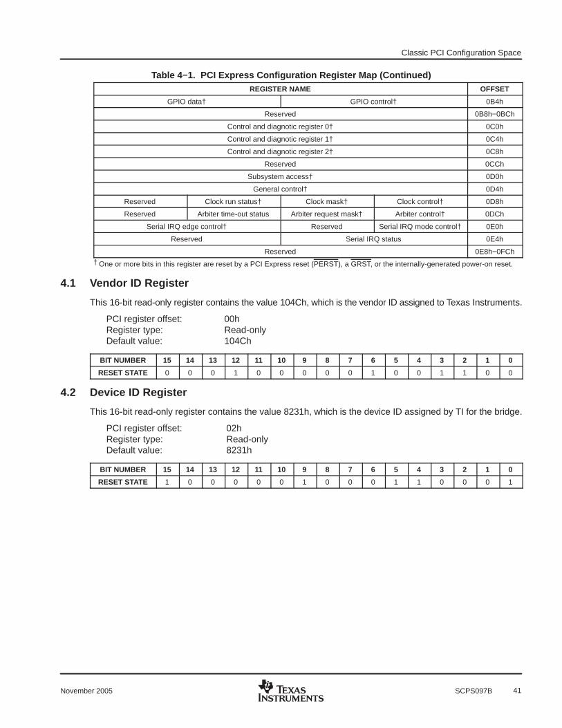
Classic PCI Configuration Space
41November 2005 SCPS097B
Table 4−1. PCI Express Configuration Register Map (Continued)REGISTER NAME OFFSET
GPIO data† GPIO control† 0B4h
Reserved 0B8h−0BCh
Control and diagnotic register 0† 0C0h
Control and diagnotic register 1† 0C4h
Control and diagnotic register 2† 0C8h
Reserved 0CCh
Subsystem access† 0D0h
General control† 0D4h
Reserved Clock run status† Clock mask† Clock control† 0D8h
Reserved Arbiter time-out status Arbiter request mask† Arbiter control† 0DCh
Serial IRQ edge control† Reserved Serial IRQ mode control† 0E0h
Reserved Serial IRQ status 0E4h
Reserved 0E8h−0FCh
† One or more bits in this register are reset by a PCI Express reset (PERST), a GRST, or the internally-generated power-on reset.
4.1 Vendor ID Register
This 16-bit read-only register contains the value 104Ch, which is the vendor ID assigned to Texas Instruments.
PCI register offset: 00hRegister type: Read-onlyDefault value: 104Ch
BIT NUMBER 15 14 13 12 11 10 9 8 7 6 5 4 3 2 1 0
RESET STATE 0 0 0 1 0 0 0 0 0 1 0 0 1 1 0 0
4.2 Device ID Register
This 16-bit read-only register contains the value 8231h, which is the device ID assigned by TI for the bridge.
PCI register offset: 02hRegister type: Read-onlyDefault value: 8231h
BIT NUMBER 15 14 13 12 11 10 9 8 7 6 5 4 3 2 1 0
RESET STATE 1 0 0 0 0 0 1 0 0 0 1 1 0 0 0 1
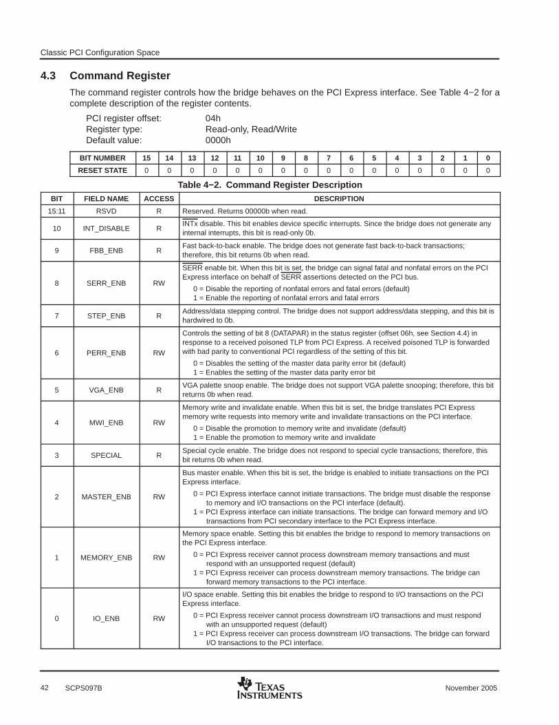
Classic PCI Configuration Space
42 November 2005SCPS097B
4.3 Command RegisterThe command register controls how the bridge behaves on the PCI Express interface. See Table 4−2 for acomplete description of the register contents.
PCI register offset: 04hRegister type: Read-only, Read/WriteDefault value: 0000h
BIT NUMBER 15 14 13 12 11 10 9 8 7 6 5 4 3 2 1 0
RESET STATE 0 0 0 0 0 0 0 0 0 0 0 0 0 0 0 0
Table 4−2. Command Register DescriptionBIT FIELD NAME ACCESS DESCRIPTION
15:11 RSVD R Reserved. Returns 00000b when read.
10 INT_DISABLE RINTx disable. This bit enables device specific interrupts. Since the bridge does not generate anyinternal interrupts, this bit is read-only 0b.
9 FBB_ENB RFast back-to-back enable. The bridge does not generate fast back-to-back transactions;therefore, this bit returns 0b when read.
8 SERR_ENB RW
SERR enable bit. When this bit is set, the bridge can signal fatal and nonfatal errors on the PCIExpress interface on behalf of SERR assertions detected on the PCI bus.
0 = Disable the reporting of nonfatal errors and fatal errors (default)1 = Enable the reporting of nonfatal errors and fatal errors
7 STEP_ENB RAddress/data stepping control. The bridge does not support address/data stepping, and this bit ishardwired to 0b.
6 PERR_ENB RW
Controls the setting of bit 8 (DATAPAR) in the status register (offset 06h, see Section 4.4) inresponse to a received poisoned TLP from PCI Express. A received poisoned TLP is forwardedwith bad parity to conventional PCI regardless of the setting of this bit.
0 = Disables the setting of the master data parity error bit (default)1 = Enables the setting of the master data parity error bit
5 VGA_ENB RVGA palette snoop enable. The bridge does not support VGA palette snooping; therefore, this bitreturns 0b when read.
4 MWI_ENB RW
Memory write and invalidate enable. When this bit is set, the bridge translates PCI Expressmemory write requests into memory write and invalidate transactions on the PCI interface.
0 = Disable the promotion to memory write and invalidate (default)1 = Enable the promotion to memory write and invalidate
3 SPECIAL RSpecial cycle enable. The bridge does not respond to special cycle transactions; therefore, thisbit returns 0b when read.
2 MASTER_ENB RW
Bus master enable. When this bit is set, the bridge is enabled to initiate transactions on the PCIExpress interface.
0 = PCI Express interface cannot initiate transactions. The bridge must disable the response to memory and I/O transactions on the PCI interface (default).
1 = PCI Express interface can initiate transactions. The bridge can forward memory and I/O transactions from PCI secondary interface to the PCI Express interface.
1 MEMORY_ENB RW
Memory space enable. Setting this bit enables the bridge to respond to memory transactions onthe PCI Express interface.
0 = PCI Express receiver cannot process downstream memory transactions and must respond with an unsupported request (default)
1 = PCI Express receiver can process downstream memory transactions. The bridge can forward memory transactions to the PCI interface.
0 IO_ENB RW
I/O space enable. Setting this bit enables the bridge to respond to I/O transactions on the PCIExpress interface.
0 = PCI Express receiver cannot process downstream I/O transactions and must respond with an unsupported request (default)
1 = PCI Express receiver can process downstream I/O transactions. The bridge can forward I/O transactions to the PCI interface.

Classic PCI Configuration Space
43November 2005 SCPS097B
4.4 Status Register
The status register provides information about the PCI Express interface to the system. See Table 4−3 for acomplete description of the register contents.
PCI register offset: 06hRegister type: Read-only, Read/ClearDefault value: 0010h
BIT NUMBER 15 14 13 12 11 10 9 8 7 6 5 4 3 2 1 0
RESET STATE 0 0 0 0 0 0 0 0 0 0 0 1 0 0 0 0
Table 4−3. Status Register DescriptionBIT FIELD NAME ACCESS DESCRIPTION
15 PAR_ERR RCU
Detected parity error. This bit is set when the PCI Express interface receives a poisoned TLP. Thisbit is set regardless of the state of bit 6 (PERR_ENB) in the command register (offset 04h, seeSection 4.3).
0 = No parity error detected1 = Parity error detected
14 SYS_ERR RCU
Signaled system error. This bit is set when the bridge sends an ERR_FATAL or ERR_NONFATALmessage and bit 8 (SERR_ENB) in the command register (offset 04h, see Section 4.3) is set.
0 = No error signaled1 = ERR_FATAL or ERR_NONFATAL signaled
13 MABORT RCU
Received master abort. This bit is set when the PCI Express interface of the bridge receives acompletion-with-unsupported-request status.
0 = Unsupported request not received on the PCI Express interface1 = Unsupported request received on the PCI Express interface
12 TABORT_REC RCU
Received target abort. This bit is set when the PCI Express interface of the bridge receives acompletion-with-completer-abort status.
0 = Completer abort not received on the PCI Express interface1 = Completer abort received on the PCI Express interface
11 TABORT_SIG RCU
Signaled target abort. This bit is set when the PCI Express interface completes a request withcompleter abort status.
0 = Completer abort not signaled on the PCI Express interface1 = Completer abort signaled on the PCI Express interface
10:9 PCI_SPEED R DEVSEL timing. These bits are read-only 00b, because they do not apply to PCI Express.
8 DATAPAR RCU
Master data parity error. This bit is set if bit 6 (PERR_ENB) in the command register (offset 04h,see Section 4.3) is set and the bridge receives a completion with data marked as poisoned on thePCI Express interface or poisons a write request received on the PCI Express interface.
0 = No uncorrectable data error detected on the primary interface1 = Uncorrectable data error detected on the primary interface
7 FBB_CAP RFast back-to-back capable. This bit does not have a meaningful context for a PCI Express deviceand is hardwired to 0b.
6 RSVD R Reserved. Returns 0b when read.
5 66MHZ R66-MHz capable. This bit does not have a meaningful context for a PCI Express device and ishardwired to 0b.
4 CAPLIST RCapabilities list. This bit returns 1b when read, indicating that the bridge supports additional PCIcapabilities.
3 INT_STATUS RInterrupt status. This bit reflects the interrupt status of the function. This bit is read-only 0b sincethe bridge does not generate any interrupts internally.
2:0 RSVD R Reserved. Returns 000b when read.

Classic PCI Configuration Space
44 November 2005SCPS097B
4.5 Class Code and Revision ID Register
This read-only register categorizes the base class, subclass, and programming interface of the bridge. Thebase class is 06h, identifying the device as a bridge. The subclass is 04h, identifying the function as aPCI-to-PCI bridge, and the programming interface is 00h. Furthermore, the TI device revision is indicated inthe lower byte (02h). See Table 4−4 for a complete description of the register contents.
PCI register offset: 08hRegister type: Read-onlyDefault value: 0604 0002h
BIT NUMBER 31 30 29 28 27 26 25 24 23 22 21 20 19 18 17 16
RESET STATE 0 0 0 0 0 1 1 0 0 0 0 0 0 1 0 0
BIT NUMBER 15 14 13 12 11 10 9 8 7 6 5 4 3 2 1 0
RESET STATE 0 0 0 0 0 0 0 0 0 0 0 0 0 0 1 0
Table 4−4. Class Code and Revision ID Register DescriptionBIT FIELD NAME ACCESS DESCRIPTION
31:24 BASECLASS R Base class. This field returns 06h when read, which classifies the function as a bridge device.
23:16 SUBCLASS R Subclass. This field returns 04h when read, which classifies the function as a PCI-to-PCI bridge.
15:8 PGMIF R Programming interface. This field returns 00h when read.
7:0 CHIPREV R Silicon revision. This field returns the silicon revision of the function.
4.6 Cache Line Size Register
This read/write cache line size register is used by the bridge to determine how much data to prefetch whenhandling delayed read transactions. The value in this register must be programmed to a power of 2. Any writtenodd value (bit 0 = 1b) or value greater than 32 DWORDs is treated as 0 DWORDs.
PCI register offset: 0ChRegister type: Read/WriteDefault value: 00h
BIT NUMBER 7 6 5 4 3 2 1 0
RESET STATE 0 0 0 0 0 0 0 0
4.7 Primary Latency Timer Register
This read-only register has no meaningful context for a PCI Express device and returns the value 00h whenread.
PCI register offset: 0DhRegister type: Read-onlyDefault value: 00h
BIT NUMBER 7 6 5 4 3 2 1 0
RESET STATE 0 0 0 0 0 0 0 0
4.8 Header Type Register
This read-only register indicates that this function has a type one PCI header. Bit 7 of this register is 0bindicating that the bridge is a single-function device.
PCI register offset: 0EhRegister type: Read-onlyDefault value: 01h
BIT NUMBER 7 6 5 4 3 2 1 0
RESET STATE 0 0 0 0 0 0 0 1

Classic PCI Configuration Space
45November 2005 SCPS097B
4.9 BIST Register
Since the bridge does not support a built-in self test (BIST), this read-only register returns the value of 00hwhen read.
PCI register offset: 0FhRegister type: Read-onlyDefault value: 00h
BIT NUMBER 7 6 5 4 3 2 1 0
RESET STATE 0 0 0 0 0 0 0 0
4.10 Device Control Base Address Register
This read/write register programs the memory base address that accesses the device control registers. SeeTable 4−5 for a complete description of the register contents.
PCI register offset: 10hRegister type: Read-only, Read/WriteDefault value: 0000 0000h
BIT NUMBER 31 30 29 28 27 26 25 24 23 22 21 20 19 18 17 16
RESET STATE 0 0 0 0 0 0 0 0 0 0 0 0 0 0 0 0
BIT NUMBER 15 14 13 12 11 10 9 8 7 6 5 4 3 2 1 0
RESET STATE 0 0 0 0 0 0 0 0 0 0 0 0 0 0 0 0
Table 4−5. Device Control Base Address Register DescriptionBIT FIELD NAME ACCESS DESCRIPTION
31:12 ADDRESS RWMemory base address. The memory address field for the bridge uses 20 read/write bits indicatingthat 4096 bytes is the amount of memory space that is reserved.
11:4 RSVD R Reserved. These bits are read-only and return 00h when read.
3 PRE_FETCH R Prefetchable. This bit is read-only 0b indicating that this memory window is not prefetchable.
2:1 MEM_TYPE RMemory type. This field is read-only 00b indicating that this window can be located anywhere in the32-bit address space.
0 MEM_IND R Memory space indicator. This field returns 0b indicating that memory space is used.
4.11 Primary Bus Number Register
This read/write register specifies the bus number of the PCI bus segment that the PCI Express interface isconnected to.
PCI register offset: 18hRegister type: Read/WriteDefault value: 00h
BIT NUMBER 7 6 5 4 3 2 1 0
RESET STATE 0 0 0 0 0 0 0 0
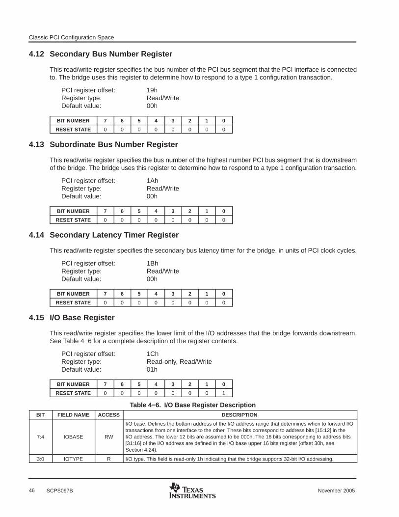
Classic PCI Configuration Space
46 November 2005SCPS097B
4.12 Secondary Bus Number Register
This read/write register specifies the bus number of the PCI bus segment that the PCI interface is connectedto. The bridge uses this register to determine how to respond to a type 1 configuration transaction.
PCI register offset: 19hRegister type: Read/WriteDefault value: 00h
BIT NUMBER 7 6 5 4 3 2 1 0
RESET STATE 0 0 0 0 0 0 0 0
4.13 Subordinate Bus Number Register
This read/write register specifies the bus number of the highest number PCI bus segment that is downstreamof the bridge. The bridge uses this register to determine how to respond to a type 1 configuration transaction.
PCI register offset: 1AhRegister type: Read/WriteDefault value: 00h
BIT NUMBER 7 6 5 4 3 2 1 0
RESET STATE 0 0 0 0 0 0 0 0
4.14 Secondary Latency Timer Register
This read/write register specifies the secondary bus latency timer for the bridge, in units of PCI clock cycles.
PCI register offset: 1BhRegister type: Read/WriteDefault value: 00h
BIT NUMBER 7 6 5 4 3 2 1 0
RESET STATE 0 0 0 0 0 0 0 0
4.15 I/O Base Register
This read/write register specifies the lower limit of the I/O addresses that the bridge forwards downstream.See Table 4−6 for a complete description of the register contents.
PCI register offset: 1ChRegister type: Read-only, Read/WriteDefault value: 01h
BIT NUMBER 7 6 5 4 3 2 1 0
RESET STATE 0 0 0 0 0 0 0 1
Table 4−6. I/O Base Register DescriptionBIT FIELD NAME ACCESS DESCRIPTION
7:4 IOBASE RW
I/O base. Defines the bottom address of the I/O address range that determines when to forward I/Otransactions from one interface to the other. These bits correspond to address bits [15:12] in theI/O address. The lower 12 bits are assumed to be 000h. The 16 bits corresponding to address bits[31:16] of the I/O address are defined in the I/O base upper 16 bits register (offset 30h, seeSection 4.24).
3:0 IOTYPE R I/O type. This field is read-only 1h indicating that the bridge supports 32-bit I/O addressing.
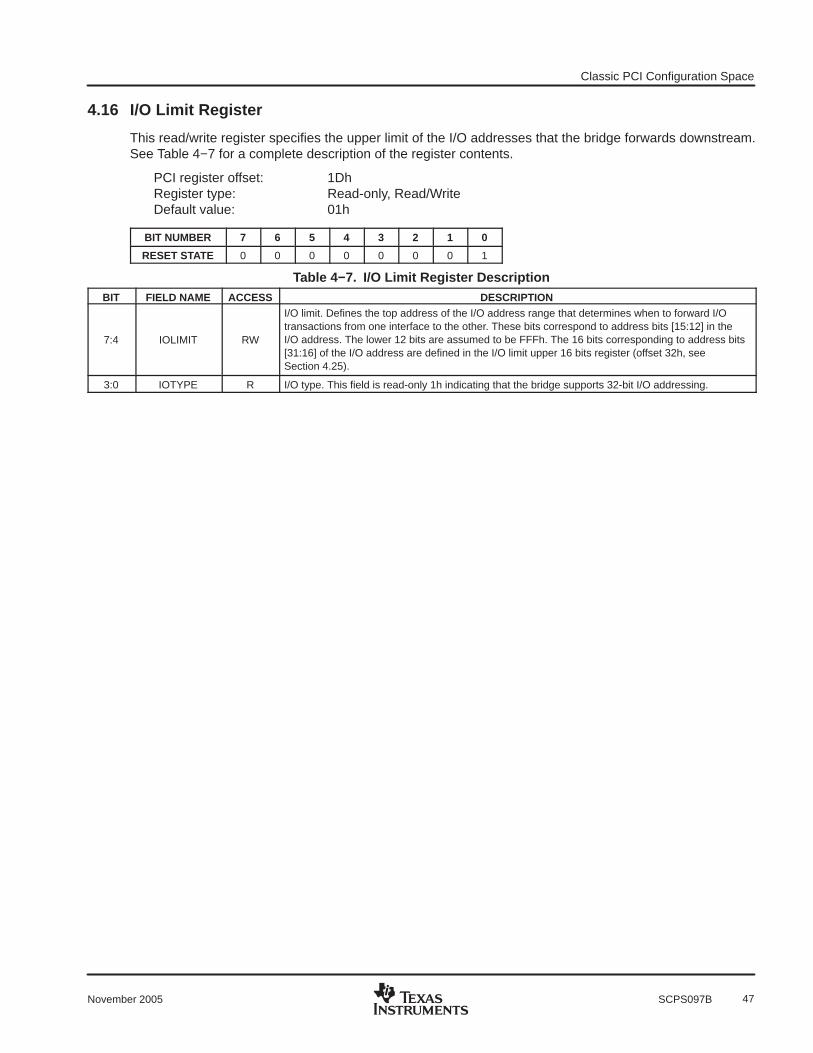
Classic PCI Configuration Space
47November 2005 SCPS097B
4.16 I/O Limit Register
This read/write register specifies the upper limit of the I/O addresses that the bridge forwards downstream.See Table 4−7 for a complete description of the register contents.
PCI register offset: 1DhRegister type: Read-only, Read/WriteDefault value: 01h
BIT NUMBER 7 6 5 4 3 2 1 0
RESET STATE 0 0 0 0 0 0 0 1
Table 4−7. I/O Limit Register DescriptionBIT FIELD NAME ACCESS DESCRIPTION
7:4 IOLIMIT RW
I/O limit. Defines the top address of the I/O address range that determines when to forward I/Otransactions from one interface to the other. These bits correspond to address bits [15:12] in theI/O address. The lower 12 bits are assumed to be FFFh. The 16 bits corresponding to address bits[31:16] of the I/O address are defined in the I/O limit upper 16 bits register (offset 32h, seeSection 4.25).
3:0 IOTYPE R I/O type. This field is read-only 1h indicating that the bridge supports 32-bit I/O addressing.

Classic PCI Configuration Space
48 November 2005SCPS097B
4.17 Secondary Status Register
The secondary status register provides information about the PCI bus interface. See Table 4−8 for a completedescription of the register contents.
PCI register offset: 1EhRegister type: Read-only, Read/ClearDefault value: 02X0h
BIT NUMBER 15 14 13 12 11 10 9 8 7 6 5 4 3 2 1 0
RESET STATE 0 0 0 0 0 0 1 0 1 0 x 0 0 0 0 0
Table 4−8. Secondary Status Register DescriptionBIT FIELD NAME ACCESS DESCRIPTION
15 PAR_ERR RCU Detected parity error. This bit reports the detection of an uncorrectable address, attribute, or dataerror by the bridge on its secondary interface. This bit must be set when any of the following threeconditions are true:• The bridge detects an uncorrectable address or attribute error as a potential target.
• The bridge detects an uncorrectable data error when it is the target of a write transaction.
• The bridge detects an uncorrectable data error when it is the master of a read transaction
(immediate read data).
The bit is set irrespective of the state of bit 0 (PERR_EN) in the bridge control register at offset 3Eh(see Section 4.29).
0 = Uncorrectable address, attribute, or data error not detected on secondary interface1 = Uncorrectable address, attribute, or data error detected on secondary interface
14 SYS_ERR RCU Received system error. This bit is set when the bridge detects an SERR assertion.
0 = No error asserted on the PCI interface1 = SERR asserted on the PCI interface
13 MABORT RCU Received master abort. This bit is set when the PCI interface of the bridge reports the detection ofa master abort termination by the bridge when it is the master of a transaction on its secondaryinterface.
0 = Master abort not received on the PCI interface1 = Master abort received on the PCI interface
12 TABORT_REC RCU Received target abort. This bit is set when the PCI interface of the bridge receives a target abort.
0 = Target abort not received on the PCI interface1 = Target abort received on the PCI interface
11 TABORT_SIG RCU Signaled target abort. This bit reports the signaling of a target abort termination by the bridge whenit responds as the target of a transaction on its secondary interface.
0 = Target abort not signaled on the PCI interface1 = Target abort signaled on the PCI interface
10:9 PCI_SPEED R DEVSEL timing. These bits are 01b indicating that this is a medium speed decoding device.
8 DATAPAR RCU Master data parity error. This bit is set if the bridge is the bus master of the transaction on the PCIbus, bit 0 (PERR_EN) in the bridge control register (offset 3Eh see Section 4.29) is set, and thebridge either asserts PERR on a read transaction or detects PERR asserted on a write transaction.
0 = No data parity error detected on the PCI interface1 = Data parity error detected on the PCI interface
7 FBB_CAP R Fast back-to-back capable. This bit returns a 1b when read indicating that the secondary PCIinterface of bridge supports fast back-to-back transactions.
6 RSVD R Reserved. Returns 0b when read.
5 66MHZ R 66-MHz capable. The bridge can operate at a maximum CLK frequency of 66 MHz; therefore, thisbit reflects the state of the M66EN terminal.
4:0 RSVD R Reserved. Returns 00000b when read.

Classic PCI Configuration Space
49November 2005 SCPS097B
4.18 Memory Base Register
This read/write register specifies the lower limit of the memory addresses that the bridge forwardsdownstream. See Table 4−9 for a complete description of the register contents.
PCI register offset: 20hRegister type: Read-only, Read/WriteDefault value: 0000h
BIT NUMBER 15 14 13 12 11 10 9 8 7 6 5 4 3 2 1 0
RESET STATE 0 0 0 0 0 0 0 0 0 0 0 0 0 0 0 0
Table 4−9. Memory Base Register DescriptionBIT FIELD NAME ACCESS DESCRIPTION
15:4 MEMBASE RWMemory base. Defines the lowest address of the memory address range that determines when toforward memory transactions from one interface to the other. These bits correspond to address bits[31:20] in the memory address. The lower 20 bits are assumed to be 00000h.
3:0 RSVD R Reserved. Returns 0h when read.
4.19 Memory Limit Register
This read/write register specifies the upper limit of the memory addresses that the bridge forwardsdownstream. See Table 4−10 for a complete description of the register contents.
PCI register offset: 22hRegister type: Read-only, Read/WriteDefault value: 0000h
BIT NUMBER 15 14 13 12 11 10 9 8 7 6 5 4 3 2 1 0
RESET STATE 0 0 0 0 0 0 0 0 0 0 0 0 0 0 0 0
Table 4−10. Memory Limit Register DescriptionBIT FIELD NAME ACCESS DESCRIPTION
15:4 MEMLIMIT RWMemory limit. Defines the highest address of the memory address range that determines when toforward memory transactions from one interface to the other. These bits correspond to address bits[31:20] in the memory address. The lower 20 bits are assumed to be FFFFFh.
3:0 RSVD R Reserved. Returns 0h when read.
4.20 Prefetchable Memory Base Register
This read/write register specifies the lower limit of the prefetchable memory addresses that the bridge forwardsdownstream. See Table 4−11 for a complete description of the register contents.
PCI register offset: 24hRegister type: Read-only, Read/WriteDefault value: 0001h
BIT NUMBER 15 14 13 12 11 10 9 8 7 6 5 4 3 2 1 0
RESET STATE 0 0 0 0 0 0 0 0 0 0 0 0 0 0 0 1
Table 4−11. Prefetchable Memory Base Register DescriptionBIT FIELD NAME ACCESS DESCRIPTION
15:4 PREBASE RW
Prefetchable memory base. Defines the lowest address of the prefetchable memory address rangethat determines when to forward memory transactions from one interface to the other. These bitscorrespond to address bits [31:20] in the memory address. The lower 20 bits are assumed to be00000h. The prefetchable base upper 32 bits register (offset 28h, see Section 4.22) specifiesbits [63:32] of the 64-bit prefetchable memory address.
3:0 64BIT R64-bit memory indicator. These read-only bits indicate that 64-bit addressing is supported for thismemory window.

Classic PCI Configuration Space
50 November 2005SCPS097B
4.21 Prefetchable Memory Limit RegisterThis read/write register specifies the upper limit of the prefetchable memory addresses that the bridgeforwards downstream. See Table 4−12 for a complete description of the register contents.
PCI register offset: 26hRegister type: Read-only, Read/WriteDefault value: 0001h
BIT NUMBER 15 14 13 12 11 10 9 8 7 6 5 4 3 2 1 0
RESET STATE 0 0 0 0 0 0 0 0 0 0 0 0 0 0 0 1
Table 4−12. Prefetchable Memory Limit Register DescriptionBIT FIELD NAME ACCESS DESCRIPTION
15:4 PRELIMIT RW
Prefetchable memory limit. Defines the highest address of the prefetchable memory address rangethat determines when to forward memory transactions from one interface to the other. These bitscorrespond to address bits [31:20] in the memory address. The lower 20 bits are assumed to beFFFFFh. The prefetchable limit upper 32 bits register (offset 2Ch, see Section 4.23) specifies bits[63:32] of the 64-bit prefetchable memory address.
3:0 64BIT R64-bit memory indicator. These read-only bits indicate that 64-bit addressing is supported for thismemory window.
4.22 Prefetchable Base Upper 32-Bit RegisterThis read/write register specifies the upper 32 bits of the prefetchable memory base register. See Table 4−13for a complete description of the register contents.
PCI register offset: 28hRegister type: Read/WriteDefault value: 0000 0000h
BIT NUMBER 31 30 29 28 27 26 25 24 23 22 21 20 19 18 17 16
RESET STATE 0 0 0 0 0 0 0 0 0 0 0 0 0 0 0 0
BIT NUMBER 15 14 13 12 11 10 9 8 7 6 5 4 3 2 1 0
RESET STATE 0 0 0 0 0 0 0 0 0 0 0 0 0 0 0 0
Table 4−13. Prefetchable Base Upper 32-Bit Register DescriptionBIT FIELD NAME ACCESS DESCRIPTION
31:0 PREBASE RWPrefetchable memory base upper 32 bits. Defines the upper 32 bits of the lowest address of theprefetchable memory address range that determines when to forward memory transactionsdownstream.
4.23 Prefetchable Limit Upper 32-Bit RegisterThis read/write register specifies the upper 32 bits of the prefetchable memory limit register. See Table 4−14for a complete description of the register contents.
PCI register offset: 2ChRegister type: Read/WriteDefault value: 0000 0000h
BIT NUMBER 31 30 29 28 27 26 25 24 23 22 21 20 19 18 17 16
RESET STATE 0 0 0 0 0 0 0 0 0 0 0 0 0 0 0 0
BIT NUMBER 15 14 13 12 11 10 9 8 7 6 5 4 3 2 1 0
RESET STATE 0 0 0 0 0 0 0 0 0 0 0 0 0 0 0 0
Table 4−14. Prefetchable Limit Upper 32-Bit Register DescriptionBIT FIELD NAME ACCESS DESCRIPTION
31:0 PRELIMIT RWPrefetchable memory limit upper 32 bits. Defines the upper 32 bits of the highest address of theprefetchable memory address range that determines when to forward memory transactionsdownstream.

Classic PCI Configuration Space
51November 2005 SCPS097B
4.24 I/O Base Upper 16-Bit Register
This read/write register specifies the upper 16 bits of the I/O base register. See Table 4−15 for a completedescription of the register contents.
PCI register offset: 30hRegister type: Read/WriteDefault value: 0000h
BIT NUMBER 15 14 13 12 11 10 9 8 7 6 5 4 3 2 1 0
RESET STATE 0 0 0 0 0 0 0 0 0 0 0 0 0 0 0 0
Table 4−15. I/O Base Upper 16-Bit Register DescriptionBIT FIELD NAME ACCESS DESCRIPTION
15:0 IOBASE RWI/O base upper 16 bits. Defines the upper 16 bits of the lowest address of the I/O address rangethat determines when to forward I/O transactions downstream. These bits correspond to addressbits [31:20] in the I/O address. The lower 20 bits are assumed to be 00000h.
4.25 I/O Limit Upper 16-Bit Register
This read/write register specifies the upper 16 bits of the I/O limit register. See Table 4−16 for a completedescription of the register contents.
PCI register offset: 32hRegister type: Read/WriteDefault value: 0000h
BIT NUMBER 15 14 13 12 11 10 9 8 7 6 5 4 3 2 1 0
RESET STATE 0 0 0 0 0 0 0 0 0 0 0 0 0 0 0 0
Table 4−16. I/O Limit Upper 16-Bit Register DescriptionBIT FIELD NAME ACCESS DESCRIPTION
15:0 IOLIMIT RWI/O limit upper 16 bits. Defines the upper 16 bits of the top address of the I/O address range thatdetermines when to forward I/O transactions downstream. These bits correspond to addressbits [31:20] in the I/O address. The lower 20 bits are assumed to be FFFFFh.
4.26 Capabilities Pointer Register
This read-only register provides a pointer into the PCI configuration header where the PCI power managementblock resides. Since the PCI power management registers begin at 50h, this register is hardwired to 50h.
PCI register offset: 34hRegister type: Read-onlyDefault value: 50h
BIT NUMBER 7 6 5 4 3 2 1 0
RESET STATE 0 1 0 1 0 0 0 0
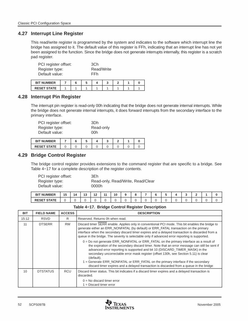
Classic PCI Configuration Space
52 November 2005SCPS097B
4.27 Interrupt Line Register
This read/write register is programmed by the system and indicates to the software which interrupt line thebridge has assigned to it. The default value of this register is FFh, indicating that an interrupt line has not yetbeen assigned to the function. Since the bridge does not generate interrupts internally, this register is a scratchpad register.
PCI register offset: 3ChRegister type: Read/WriteDefault value: FFh
BIT NUMBER 7 6 5 4 3 2 1 0
RESET STATE 1 1 1 1 1 1 1 1
4.28 Interrupt Pin Register
The interrupt pin register is read-only 00h indicating that the bridge does not generate internal interrupts. Whilethe bridge does not generate internal interrupts, it does forward interrupts from the secondary interface to theprimary interface.
PCI register offset: 3DhRegister type: Read-onlyDefault value: 00h
BIT NUMBER 7 6 5 4 3 2 1 0
RESET STATE 0 0 0 0 0 0 0 0
4.29 Bridge Control Register
The bridge control register provides extensions to the command register that are specific to a bridge. SeeTable 4−17 for a complete description of the register contents.
PCI register offset: 3EhRegister type: Read-only, Read/Write, Read/ClearDefault value: 0000h
BIT NUMBER 15 14 13 12 11 10 9 8 7 6 5 4 3 2 1 0
RESET STATE 0 0 0 0 0 0 0 0 0 0 0 0 0 0 0 0
Table 4−17. Bridge Control Register DescriptionBIT FIELD NAME ACCESS DESCRIPTION
15:12 RSVD R Reserved. Returns 0h when read.
11 DTSERR RW Discard timer SERR enable. Applies only in conventional PCI mode. This bit enables the bridge togenerate either an ERR_NONFATAL (by default) or ERR_FATAL transaction on the primaryinterface when the secondary discard timer expires and a delayed transaction is discarded from aqueue in the bridge. The severity is selectable only if advanced error reporting is supported.
0 = Do not generate ERR_NONFATAL or ERR_FATAL on the primary interface as a result of the expiration of the secondary discard timer. Note that an error message can still be sent if advanced error reporting is supported and bit 10 (DISCARD_TIMER_MASK) in the secondary uncorrectable error mask register (offset 130h, see Section 5.11) is clear (default).
1 = Generate ERR_NONFATAL or ERR_FATAL on the primary interface if the secondary discard timer expires and a delayed transaction is discarded from a queue in the bridge
10 DTSTATUS RCU Discard timer status. This bit indicates if a discard timer expires and a delayed transaction isdiscarded.
0 = No discard timer error1 = Discard timer error
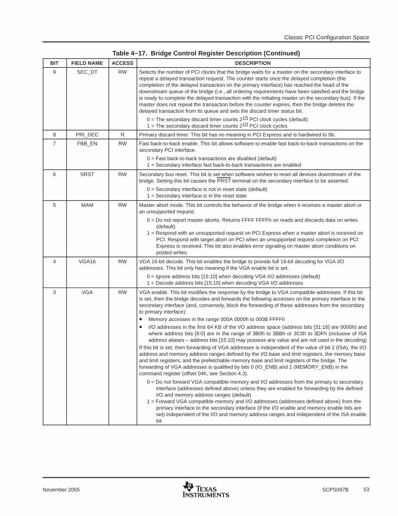
Classic PCI Configuration Space
53November 2005 SCPS097B
Table 4−17. Bridge Control Register Description (Continued)BIT FIELD NAME ACCESS DESCRIPTION
9 SEC_DT RW Selects the number of PCI clocks that the bridge waits for a master on the secondary interface torepeat a delayed transaction request. The counter starts once the delayed completion (thecompletion of the delayed transaction on the primary interface) has reached the head of thedownstream queue of the bridge (i.e., all ordering requirements have been satisfied and the bridgeis ready to complete the delayed transaction with the initiating master on the secondary bus). If themaster does not repeat the transaction before the counter expires, then the bridge deletes thedelayed transaction from its queue and sets the discard timer status bit.
0 = The secondary discard timer counts 215 PCI clock cycles (default)1 = The secondary discard timer counts 210 PCI clock cycles
8 PRI_DEC R Primary discard timer. This bit has no meaning in PCI Express and is hardwired to 0b.
7 FBB_EN RW Fast back-to-back enable. This bit allows software to enable fast back-to-back transactions on thesecondary PCI interface.
0 = Fast back-to-back transactions are disabled (default)1 = Secondary interface fast back-to-back transactions are enabled
6 SRST RW Secondary bus reset. This bit is set when software wishes to reset all devices downstream of thebridge. Setting this bit causes the PRST terminal on the secondary interface to be asserted.
0 = Secondary interface is not in reset state (default)1 = Secondary interface is in the reset state
5 MAM RW Master abort mode. This bit controls the behavior of the bridge when it receives a master abort oran unsupported request.
0 = Do not report master aborts. Returns FFFF FFFFh on reads and discards data on writes (default).
1 = Respond with an unsupported request on PCI Express when a master abort is received on PCI. Respond with target abort on PCI when an unsupported request completion on PCI Express is received. This bit also enables error signaling on master abort conditions on posted writes.
4 VGA16 RW VGA 16-bit decode. This bit enables the bridge to provide full 16-bit decoding for VGA I/Oaddresses. This bit only has meaning if the VGA enable bit is set.
0 = Ignore address bits [15:10] when decoding VGA I/O addresses (default)1 = Decode address bits [15:10] when decoding VGA I/O addresses
3 VGA RW VGA enable. This bit modifies the response by the bridge to VGA compatible addresses. If this bitis set, then the bridge decodes and forwards the following accesses on the primary interface to thesecondary interface (and, conversely, block the forwarding of these addresses from the secondaryto primary interface):• Memory accesses in the range 000A 0000h to 000B FFFFh
• I/O addresses in the first 64 KB of the I/O address space (address bits [31:16] are 0000h) andwhere address bits [9:0] are in the range of 3B0h to 3BBh or 3C0h to 3DFh (inclusive of ISAaddress aliases – address bits [15:10] may possess any value and are not used in the decoding)
If this bit is set, then forwarding of VGA addresses is independent of the value of bit 2 (ISA), the I/Oaddress and memory address ranges defined by the I/O base and limit registers, the memory baseand limit registers, and the prefetchable memory base and limit registers of the bridge. Theforwarding of VGA addresses is qualified by bits 0 (IO_ENB) and 1 (MEMORY_ENB) in thecommand register (offset 04h, see Section 4.3).
0 = Do not forward VGA compatible memory and I/O addresses from the primary to secondary interface (addresses defined above) unless they are enabled for forwarding by the defined I/O and memory address ranges (default)
1 = Forward VGA compatible memory and I/O addresses (addresses defined above) from the primary interface to the secondary interface (if the I/O enable and memory enable bits are set) independent of the I/O and memory address ranges and independent of the ISA enable bit

Classic PCI Configuration Space
54 November 2005SCPS097B
Table 4−17. Bridge Control Register Description (Continued)BIT FIELD NAME ACCESS DESCRIPTION
2 ISA RW ISA enable. This bit modifies the response by the bridge to ISA I/O addresses. This applies only toI/O addresses that are enabled by the I/O base and I/O limit registers and are in the first 64 KB ofPCI I/O address space (0000 0000h to 0000 FFFFh). If this bit is set, then the bridge blocks anyforwarding from primary to secondary of I/O transactions addressing the last 768 bytes in each1 KB block. In the opposite direction (secondary to primary), I/O transactions are forwarded if theyaddress the last 768 bytes in each 1K block.
0 = Forward downstream all I/O addresses in the address range defined by the I/O base and I/O limit registers (default)
1 = Forward upstream ISA I/O addresses in the address range defined by the I/O base and I/O limit registers that are in the first 64 KB of PCI I/O address space (top 768 bytes of each 1-KB block)
1 SERR_EN RW SERR enable. This bit controls forwarding of system error events from the secondary interface tothe primary interface. The bridge forwards system error events when:• This bit is set
• Bit 8 (SERR_ENB) in the command register (offset 04h, see Section 4.3) is set
• SERR is asserted on the secondary interface
0 = Disable the forwarding of system error events (default)1 = Enable the forwarding of system error events
0 PERR_EN RW Parity error response enable. Controls the bridge’s response to data, uncorrectable address, andattribute errors on the secondary interface. Also, the bridge always forwards data with poisoning,from conventional PCI to PCI Express on an uncorrectable conventional PCI data error, regardlessof the setting of this bit.
0 = Ignore uncorrectable address, attribute, and data errors on the secondary interface (default)
1 = Enable uncorrectable address, attribute, and data error detection and reporting on the secondary interface
4.30 Capability ID Register
This read-only register identifies the linked list item as the register for PCI power management. The registerreturns 01h when read.
PCI register offset: 50hRegister type: Read-onlyDefault value: 01h
BIT NUMBER 7 6 5 4 3 2 1 0
RESET STATE 0 0 0 0 0 0 0 1
4.31 Next Item Pointer Register
The contents of this read-only register indicate the next item in the linked list of capabilities for the bridge. Thisregister reads 60h pointing to the MSI capabilities registers.
PCI register offset: 51hRegister type: Read-onlyDefault value: 60h
BIT NUMBER 7 6 5 4 3 2 1 0
RESET STATE 0 1 1 0 0 0 0 0

Classic PCI Configuration Space
55November 2005 SCPS097B
4.32 Power Management Capabilities Register
This read-only register indicates the capabilities of the bridge related to PCI power management. SeeTable 4−18 for a complete description of the register contents.
PCI register offset: 52hRegister type: Read-onlyDefault value: 0602h
BIT NUMBER 15 14 13 12 11 10 9 8 7 6 5 4 3 2 1 0
RESET STATE 0 0 0 0 0 1 1 0 0 0 0 0 0 0 1 0
Table 4−18. Power Management Capabilities Register DescriptionBIT FIELD NAME ACCESS DESCRIPTION
15:11 PME_SUPPORT RPME support. This 5-bit field indicates the power states from which the bridge may assert PME.Because the bridge never generates a PME except on a behalf of a secondary device, this fieldis read-only and returns 00000b.
10 D2_SUPPORT R This bit returns a 1b when read, indicating that the function supports the D2 device power state.
9 D1_SUPPORT R This bit returns a 1b when read, indicating that the function supports the D1 device power state.
8:6 AUX_CURRENT R3.3 VAUX auxiliary current requirements. This field returns 000b since the bridge does notgenerate PME from D3cold.
5 DSI RDevice specific initialization. This bit returns 0b when read, indicating that the bridge does notrequire special initialization beyond the standard PCI configuration header before a generic classdriver is able to use it.
4 RSVD R Reserved. Returns 0b when read.
3 PME_CLK R PME clock. This bit returns 0b indicating that the PCI clock is not needed to generate PME.
2:0 PM_VERSION R
Power management version. If bit 26 (PCI_PM_VERSION_CTRL) in the general control register(offset D4h, see Section 4.65) is 0b, then this field returns 010b indicating revision 1.1compatibility. If PCI_PM_VERSION_CTRL is 1b, then this field returns 011b indicating revision1.2 compatibility.
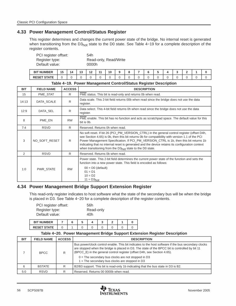
Classic PCI Configuration Space
56 November 2005SCPS097B
4.33 Power Management Control/Status Register
This register determines and changes the current power state of the bridge. No internal reset is generatedwhen transitioning from the D3hot state to the D0 state. See Table 4−19 for a complete description of theregister contents.
PCI register offset: 54hRegister type: Read-only, Read/WriteDefault value: 0000h
BIT NUMBER 15 14 13 12 11 10 9 8 7 6 5 4 3 2 1 0
RESET STATE 0 0 0 0 0 0 0 0 0 0 0 0 0 0 0 0
Table 4−19. Power Management Control/Status Register DescriptionBIT FIELD NAME ACCESS DESCRIPTION
15 PME_STAT R PME status. This bit is read-only and returns 0b when read.
14:13 DATA_SCALE RData scale. This 2-bit field returns 00b when read since the bridge does not use the dataregister.
12:9 DATA_SEL RData select. This 4-bit field returns 0h when read since the bridge does not use the dataregister.
8 PME_EN RWPME enable. This bit has no function and acts as scratchpad space. The default value for thisbit is 0b.
7:4 RSVD R Reserved. Returns 0h when read.
3 NO_SOFT_RESET R
No soft reset. If bit 26 (PCI_PM_VERSION_CTRL) in the general control register (offset D4h,see Section 4.65) is 0b, then this bit returns 0b for compatibility with version 1.1 of the PCIPower Management Specification. If PCI_PM_VERSION_CTRL is 1b, then this bit returns 1bindicating that no internal reset is generated and the device retains its configuration contextwhen transitioning from the D3hot state to the D0 state.
2 RSVD R Reserved. Returns 0b when read.
1:0 PWR_STATE RW
Power state. This 2-bit field determines the current power state of the function and sets thefunction into a new power state. This field is encoded as follows:
00 = D0 (default)01 = D110 = D211 = D3hot
4.34 Power Management Bridge Support Extension Register
This read-only register indicates to host software what the state of the secondary bus will be when the bridgeis placed in D3. See Table 4−20 for a complete description of the register contents.
PCI register offset: 56hRegister type: Read-onlyDefault value: 40h
BIT NUMBER 7 6 5 4 3 2 1 0
RESET STATE 0 1 0 0 0 0 0 0
Table 4−20. Power Management Bridge Support Extension Register DescriptionBIT FIELD NAME ACCESS DESCRIPTION
7 BPCC R
Bus power/clock control enable. This bit indicates to the host software if the bus secondary clocksare stopped when the bridge is placed in D3. The state of the BPCC bit is controlled by bit 11(BPCC_E) in the general control register (offset D4h, see Section 4.65).
0 = The secondary bus clocks are not stopped in D31 = The secondary bus clocks are stopped in D3
6 BSTATE R B2/B3 support. This bit is read-only 1b indicating that the bus state in D3 is B2.
5:0 RSVD R Reserved. Returns 00 0000b when read.

Classic PCI Configuration Space
57November 2005 SCPS097B
4.35 Power Management Data Register
The read-only register is not applicable to the bridge and returns 00h when read.
PCI register offset: 57hRegister type: Read-onlyDefault value: 00h
BIT NUMBER 7 6 5 4 3 2 1 0
RESET STATE 0 0 0 0 0 0 0 0
4.36 MSI Capability ID Register
This read-only register identifies the linked list item as the register for message signaled interrupts capabilities.The register returns 05h when read.
PCI register offset: 60hRegister type: Read-onlyDefault value: 05h
BIT NUMBER 7 6 5 4 3 2 1 0
RESET STATE 0 0 0 0 0 1 0 1
4.37 Next Item Pointer Register
The contents of this read-only register indicate the next item in the linked list of capabilities for the bridge. Thisregister reads 80h pointing to the subsystem ID capabilities registers.
PCI register offset: 61hRegister type: Read-onlyDefault value: 80h
BIT NUMBER 7 6 5 4 3 2 1 0
RESET STATE 1 0 0 0 0 0 0 0

Classic PCI Configuration Space
58 November 2005SCPS097B
4.38 MSI Message Control Register
This register controls the sending of MSI messages. See Table 4−21 for a complete description of the registercontents.
PCI register offset: 62hRegister type: Read-only, Read/WriteDefault value: 0088h
BIT NUMBER 15 14 13 12 11 10 9 8 7 6 5 4 3 2 1 0
RESET STATE 0 0 0 0 0 0 0 0 1 0 0 0 1 0 0 0
Table 4−21. MSI Message Control Register DescriptionBIT FIELD NAME ACCESS DESCRIPTION
15:8 RSVD R Reserved. Returns 00h when read.
7 64CAP R64-bit message capability. This bit is read-only 1b indicating that the bridge supports 64-bit MSImessage addressing.
6:4 MM_EN RW
Multiple message enable. This bit indicates the number of distinct messages that the bridge isallowed to generate.
000 = 1 message (default)001 = 2 messages010 = 4 messages011 = 8 messages100 = 16 messages101 = Reserved110 = Reserved111 = Reserved
3:1 MM_CAP RMultiple message capabilities. This field indicates the number of distinct messages that bridge iscapable of generating. This field is read-only 100b indicating that the bridge can signal 1 interruptfor each IRQ supported on the serial IRQ stream up to a maximum of 16 unique interrupts.
0 MSI_EN RW
MSI enable. This bit enables MSI interrupt signaling. MSI signaling must be enabled by softwarefor the bridge to signal that a serial IRQ has been detected.
0 = MSI signaling is prohibited (default)1 = MSI signaling is enabled
4.39 MSI Message Lower Address Register
This register contains the lower 32 bits of the address that a MSI message writes to when a serial IRQ isdetected. See Table 4−22 for a complete description of the register contents.
PCI register offset: 64hRegister type: Read-only, Read/WriteDefault value: 0000 0000h
BIT NUMBER 31 30 29 28 27 26 25 24 23 22 21 20 19 18 17 16
RESET STATE 0 0 0 0 0 0 0 0 0 0 0 0 0 0 0 0
BIT NUMBER 15 14 13 12 11 10 9 8 7 6 5 4 3 2 1 0
RESET STATE 0 0 0 0 0 0 0 0 0 0 0 0 0 0 0 0
Table 4−22. MSI Message Lower Address Register DescriptionBIT FIELD NAME ACCESS DESCRIPTION
31:2 ADDRESS RW System specified message address
1:0 RSVD R Reserved. Returns 00b when read.

Classic PCI Configuration Space
59November 2005 SCPS097B
4.40 MSI Message Upper Address Register
This register contains the upper 32 bits of the address that a MSI message writes to when a serial IRQ isdetected. If this register contains 0000 0000h, then 32-bit addressing is used; otherwise, 64-bit addressingis used.
PCI register offset: 68hRegister type: Read/WriteDefault value: 0000 0000h
BIT NUMBER 31 30 29 28 27 26 25 24 23 22 21 20 19 18 17 16
RESET STATE 0 0 0 0 0 0 0 0 0 0 0 0 0 0 0 0
BIT NUMBER 15 14 13 12 11 10 9 8 7 6 5 4 3 2 1 0
RESET STATE 0 0 0 0 0 0 0 0 0 0 0 0 0 0 0 0
4.41 MSI Message Data Register
This register contains the data that software programmed the bridge to send when it send a MSI message.See Table 4−23 for a complete description of the register contents.
PCI register offset: 6ChRegister type: Read/WriteDefault value: 0000h
BIT NUMBER 15 14 13 12 11 10 9 8 7 6 5 4 3 2 1 0
RESET STATE 0 0 0 0 0 0 0 0 0 0 0 0 0 0 0 0
Table 4−23. MSI Message Data Register DescriptionBIT FIELD NAME ACCESS DESCRIPTION
15:4 MSG RWSystem specific message. This field contains the portion of the message that the bridge forwardsunmodified.
3:0 MSG_NUM RW
Message number. This portion of the message field may be modified to contain the messagenumber is multiple messages are enable. The number of bits that are modifiable depends on thenumber of messages enabled in the message control register.
1 message = No message data bits can be modified (default)2 messages = Bit 0 can be modified4 messages = Bits 1:0 can be modified8 messages = Bits 2:0 can be modified16 messages = Bits 3:0 can be modified
4.42 Capability ID Register
This read-only register identifies the linked list item as the register for subsystem ID and subsystem vendorID capabilities. The register returns 0Dh when read.
PCI register offset: 80hRegister type: Read-onlyDefault value: 0Dh
BIT NUMBER 7 6 5 4 3 2 1 0
RESET STATE 0 0 0 0 1 1 0 1
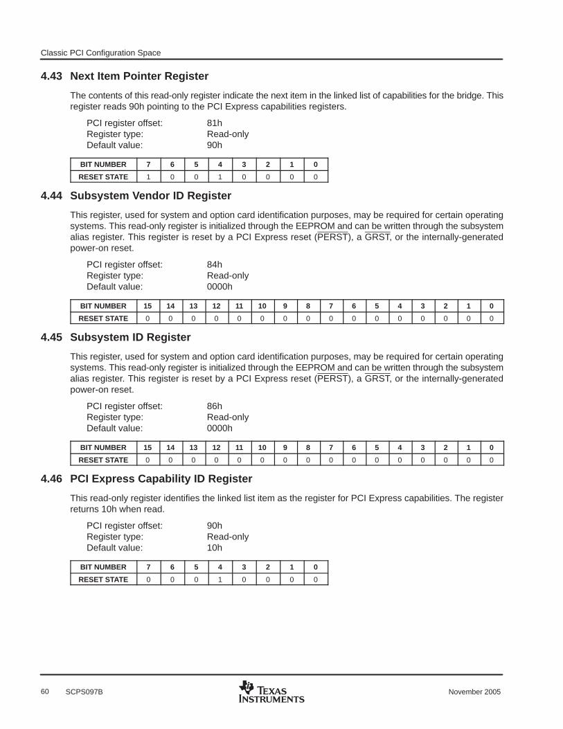
Classic PCI Configuration Space
60 November 2005SCPS097B
4.43 Next Item Pointer Register
The contents of this read-only register indicate the next item in the linked list of capabilities for the bridge. Thisregister reads 90h pointing to the PCI Express capabilities registers.
PCI register offset: 81hRegister type: Read-onlyDefault value: 90h
BIT NUMBER 7 6 5 4 3 2 1 0
RESET STATE 1 0 0 1 0 0 0 0
4.44 Subsystem Vendor ID Register
This register, used for system and option card identification purposes, may be required for certain operatingsystems. This read-only register is initialized through the EEPROM and can be written through the subsystemalias register. This register is reset by a PCI Express reset (PERST), a GRST, or the internally-generatedpower-on reset.
PCI register offset: 84hRegister type: Read-onlyDefault value: 0000h
BIT NUMBER 15 14 13 12 11 10 9 8 7 6 5 4 3 2 1 0
RESET STATE 0 0 0 0 0 0 0 0 0 0 0 0 0 0 0 0
4.45 Subsystem ID Register
This register, used for system and option card identification purposes, may be required for certain operatingsystems. This read-only register is initialized through the EEPROM and can be written through the subsystemalias register. This register is reset by a PCI Express reset (PERST), a GRST, or the internally-generatedpower-on reset.
PCI register offset: 86hRegister type: Read-onlyDefault value: 0000h
BIT NUMBER 15 14 13 12 11 10 9 8 7 6 5 4 3 2 1 0
RESET STATE 0 0 0 0 0 0 0 0 0 0 0 0 0 0 0 0
4.46 PCI Express Capability ID Register
This read-only register identifies the linked list item as the register for PCI Express capabilities. The registerreturns 10h when read.
PCI register offset: 90hRegister type: Read-onlyDefault value: 10h
BIT NUMBER 7 6 5 4 3 2 1 0
RESET STATE 0 0 0 1 0 0 0 0
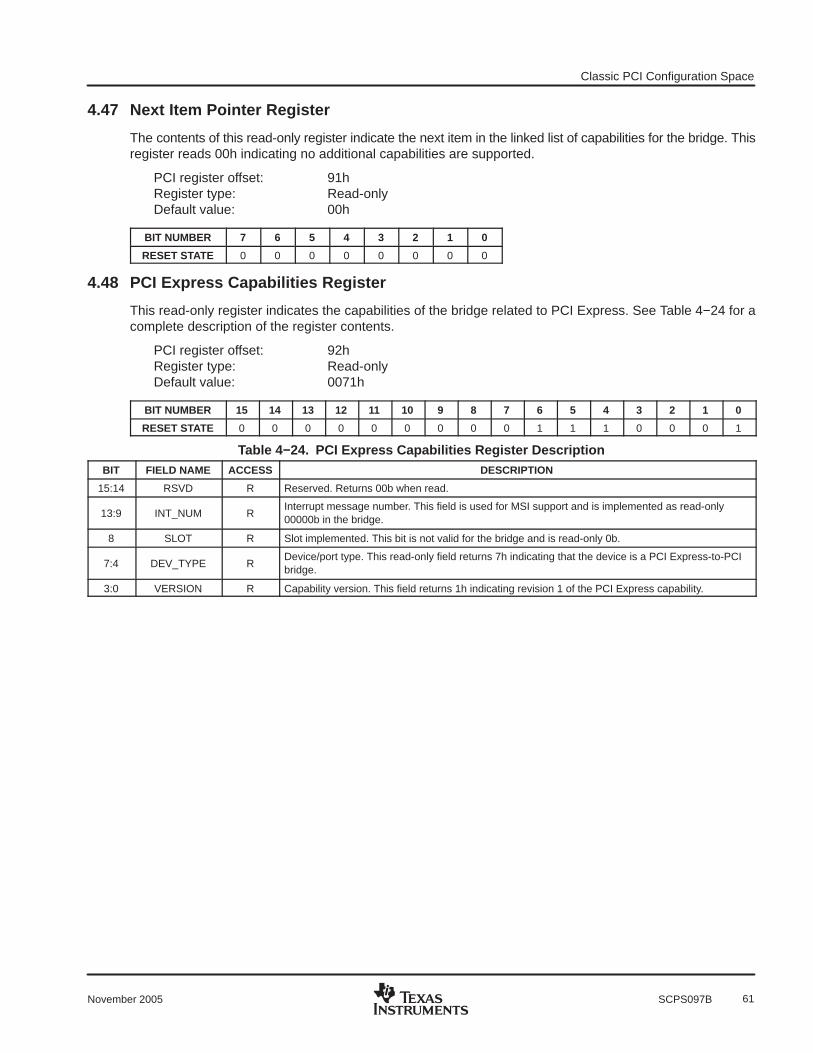
Classic PCI Configuration Space
61November 2005 SCPS097B
4.47 Next Item Pointer Register
The contents of this read-only register indicate the next item in the linked list of capabilities for the bridge. Thisregister reads 00h indicating no additional capabilities are supported.
PCI register offset: 91hRegister type: Read-onlyDefault value: 00h
BIT NUMBER 7 6 5 4 3 2 1 0
RESET STATE 0 0 0 0 0 0 0 0
4.48 PCI Express Capabilities Register
This read-only register indicates the capabilities of the bridge related to PCI Express. See Table 4−24 for acomplete description of the register contents.
PCI register offset: 92hRegister type: Read-onlyDefault value: 0071h
BIT NUMBER 15 14 13 12 11 10 9 8 7 6 5 4 3 2 1 0
RESET STATE 0 0 0 0 0 0 0 0 0 1 1 1 0 0 0 1
Table 4−24. PCI Express Capabilities Register DescriptionBIT FIELD NAME ACCESS DESCRIPTION
15:14 RSVD R Reserved. Returns 00b when read.
13:9 INT_NUM RInterrupt message number. This field is used for MSI support and is implemented as read-only00000b in the bridge.
8 SLOT R Slot implemented. This bit is not valid for the bridge and is read-only 0b.
7:4 DEV_TYPE RDevice/port type. This read-only field returns 7h indicating that the device is a PCI Express-to-PCIbridge.
3:0 VERSION R Capability version. This field returns 1h indicating revision 1 of the PCI Express capability.

Classic PCI Configuration Space
62 November 2005SCPS097B
4.49 Device Capabilities Register
The device capabilities register indicates the device specific capabilities of the bridge. See Table 4−25 for acomplete description of the register contents.
PCI register offset: 94hRegister type: Read-onlyDefault value: 0000 0D82
BIT NUMBER 31 30 29 28 27 26 25 24 23 22 21 20 19 18 17 16
RESET STATE 0 0 0 0 0 0 0 0 0 0 0 0 0 0 0 0
BIT NUMBER 15 14 13 12 11 10 9 8 7 6 5 4 3 2 1 0
RESET STATE 0 0 0 0 1 1 0 1 1 0 0 0 0 0 1 0
Table 4−25. Device Capabilities Register DescriptionBIT FIELD NAME ACCESS DESCRIPTION
31:28 RSVD R Reserved. Returns 0h when read.
27:26 CSPLS RU Captured slot power limit scale. The value in this field is programmed by the host by issuing aSet_Slot_Power_Limit message. When a Set_Slot_Power_Limit message is received, bits 9:8 arewritten to this field. The value in this field specifies the scale used for the slot power limit.
00 = 1.0x01 = 0.1x10 = 0.01x11 = 0.001x
25:18 CSPLV RU Captured slot power limit value. The value in this field is programmed by the host by issuing aSet_Slot_Power_Limit message. When a Set_Slot_Power_Limit message is received, bits 7:0 arewritten to this field. The value in this field in combination with the slot power limit scale value(bits 27:26) specifies the upper limit of power supplied to the slot. The power limit is calculated bymultiplying the value in this field by the value in the slot power limit scale field.
17:15 RSVD R Reserved. Returns 000b when read.
14 PIP R Power indicator present. This bit is hardwired to 0b indicating that a power indicator is notimplemented.
13 AIP R Attention indicator present. This bit is hardwired to 0b indicating that an attention indicator is notimplemented.
12 ABP R Attention button present. This bit is hardwired to 0b indicating that an attention button is notimplemented.
11:9 EP_L1_LAT RU Endpoint L1 acceptable latency. This field indicates the maximum acceptable latency for atransition from L1 to L0 state. This field can be programmed by writing to the L1_LATENCY field(bits 15:13) in the general control register (offset D4h, see Section 4.65). The default value for thisfield is 110b which indicates a range from 32 µs to 64 µs. This field cannot be programmed to beless than the latency for the PHY to exit the L1 state.
8:6 EP_L0S_LAT RU Endpoint L0s acceptable latency. This field indicates the maximum acceptable latency for atransition from L0s to L0 state. This field can be programmed by writing to the L0s_LATENCY field(bits 18:16) in the general control register (offset D4h, see Section 4.65). The default value for thisfield is 110b which indicates a range from 2 µs to 4 µs. This field cannot be programmed to be lessthan the latency for the PHY to exit the L0s state.
5 ETFS R Extended tag field supported. This field indicates the size of the tag field not supported.
4:3 PFS R Phantom functions supported. This field is read-only 00b indicating that function numbers are notused for phantom functions.
2:0 MPSS R Maximum payload size supported. This field indicates the maximum payload size that the devicecan support for TLPs. This field is encoded as 010b indicating the maximum payload size for a TLPis 512 bytes.

Classic PCI Configuration Space
63November 2005 SCPS097B
4.50 Device Control Register
The device control register controls PCI Express device specific parameters. See Table 4−26 for a completedescription of the register contents.
PCI register offset: 98hRegister type: Read-only, Read/WriteDefault value: 2800h
BIT NUMBER 15 14 13 12 11 10 9 8 7 6 5 4 3 2 1 0
RESET STATE 0 0 1 0 1 0 0 0 0 0 0 0 0 0 0 0
Table 4−26. Device Control Register DescriptionBIT FIELD NAME ACCESS DESCRIPTION
15 CFG_RTRY_ENB RW
Configuration retry status enable. When this read/write bit is set to 1b, the bridge returns acompletion with completion retry status on PCI Express if a configuration transaction forwardedto the secondary interface did not complete within the implementation specific time-out period.When this bit is set to 0b, the bridge does not generate completions with completion retry statuson behalf of configuration transactions. The default value of this bit is 0b.
14:12 MRRS RW
Maximum read request size. This field is programmed by host software to set the maximum sizeof a read request that the bridge can generate. The bridge uses this field in conjunction with thecache line size register (offset 0Ch, see Section 4.6) to determine how much data to fetch on aread request. This field is encoded as:
000 = 128B001 = 256B 010 = 512B (default)011 = 1024B 100 = 2048B 101 = 4096B 110 = Reserved111 = Reserved
11 ENS RW
Enable no snoop. Controls the setting of the no snoop flag within the TLP header for upstreammemory transactions mapped to any traffic class mapped to a virtual channel (VC) other thanVC0 through the upstream decode windows.
0 = No snoop field is 0b1 = No snoop field is 1b (default)
10 APPE RWAuxiliary power PM enable. This bit has no effect in the bridge.
0 = AUX power is disabled (default)1 = AUX power is enabled
9 PFE RPhantom function enable. Since the bridge does not support phantom functions, this bit isread-only 0b.
8 ETFE RExtended tag field enable. Since the bridge does not support extended tags, this bit is read-only0b.
7:5 MPS RW
Maximum payload size. This field is programmed by host software to set the maximum size ofposted writes or read completions that the bridge can initiate. This field is encoded as:
000 = 128B (default) 001 = 256B 010 = 512B 011 = 1024B 100 = 2048B 101 = 4096B 110 = Reserved111 = Reserved
4 ERO REnable relaxed ordering. Since the bridge does not support relaxed ordering, this bit is read-only0b.
This bit is sticky and must retain its value when the bridge is powered by VAUX.

Classic PCI Configuration Space
64 November 2005SCPS097B
Table 4−26. Device Control Register Description (Continued)BIT FIELD NAME ACCESS DESCRIPTION
3 URRE RW
Unsupported request reporting enable. If this bit is set, then the bridge sends an ERR_NONFATALmessage to the root complex when an unsupported request is received.
0 = Do not report unsupported requests to the root complex (default)1 = Report unsupported requests to the root complex
2 FERE RW
Fatal error reporting enable. If this bit is set, then the bridge is enabled to send ERR_FATALmessages to the root complex when a system error event occurs.
0 = Do not report fatal errors to the root complex (default)1 = Report fatal errors to the root complex
1 NFERE RW
Nonfatal error reporting enable. If this bit is set, then the bridge is enabled to sendERR_NONFATAL messages to the root complex when a system error event occurs.
0 = Do not report nonfatal errors to the root complex (default)1 = Report nonfatal errors to the root complex
0 CERE RW
Correctable error reporting enable. If this bit is set, then the bridge is enabled to send ERR_CORmessages to the root complex when a system error event occurs.
0 = Do not report correctable errors to the root complex (default)1 = Report correctable errors to the root complex
4.51 Device Status Register
The device status register provides PCI Express device specific information to the system. See Table 4−27for a complete description of the register contents.
PCI register offset: 9AhRegister type: Read-onlyDefault value: 0000h
BIT NUMBER 15 14 13 12 11 10 9 8 7 6 5 4 3 2 1 0
RESET STATE 0 0 0 0 0 0 0 0 0 0 0 0 0 0 0 0
Table 4−27. Device Status Register DescriptionBIT FIELD NAME ACCESS DESCRIPTION15:6 RSVD R Reserved. Returns 00 0000 0000b when read.
5 PEND RUTransaction pending. This bit is set when the bridge has issued a nonposted transaction that hasnot been completed.
4 APD RUAUX power detected. This bit indicates that AUX power is present.
0 = No AUX power detected1 = AUX power detected
3 URD RCUUnsupported request detected. This bit is set by the bridge when an unsupported request isreceived.
2 FED RCU Fatal error detected. This bit is set by the bridge when a fatal error is detected.
1 NFED RCU Nonfatal error detected. This bit is set by the bridge when a nonfatal error is detected.
0 CED RCU Correctable error detected. This bit is set by the bridge when a correctable error is detected.

Classic PCI Configuration Space
65November 2005 SCPS097B
4.52 Link Capabilities Register
The link capabilities register indicates the link specific capabilities of the bridge. See Table 4−28 for a completedescription of the register contents.
PCI register offset: 9ChRegister type: Read-onlyDefault value: 0002 XC11h
BIT NUMBER 31 30 29 28 27 26 25 24 23 22 21 20 19 18 17 16
RESET STATE 0 0 0 0 0 0 0 0 0 0 0 0 0 0 1 0
BIT NUMBER 15 14 13 12 11 10 9 8 7 6 5 4 3 2 1 0
RESET STATE 0 x x x 1 1 0 0 0 0 0 1 0 0 0 1
Table 4−28. Link Capabilities Register DescriptionBIT FIELD NAME ACCESS DESCRIPTION
31:24 PORT_NUM RPort number. This field indicates port number for the PCI Express link. This field is read-only 00hindicating that the link is associated with port 0.
23:18 RSVD R Reserved. Returns 00 0000b when read.
17:15 L1_LATENCY R
L1 exit latency. This field indicates the time that it takes to transition from the L1 state to the L0state. Bit 6 (CCC) in the link control register (offset A0h, see Section 4.53) equals 1b for a commonclock and equals 0b for an asynchronous clock.
For a common reference clock, the value of this field is determined by bits 20:18(L1_EXIT_LAT_ASYNC) of the control and diagnostic register 1 (offset C4h, see Section 4.62).
For an asynchronous reference clock, the value of this field is determined by bits 17:15(L1_EXIT_LAT_COMMON) of the control and diagnostic register 1 (offset C4h, see Section 4.62).
14:12 L0S_LATENCY R
L0s exit latency. This field indicates the time that it takes to transition from the L0s state to the L0state. Bit 6 (CCC) in the link control register (offset A0h, see Section 4.53) equals 1b for a commonclock and equals 0b for an asynchronous clock.
For a common reference clock, the value of 011b indicates that the L1 exit latency falls between256 ns to less than 512 ns.
For an asynchronous reference clock, the value of 100b indicates that the L1 exit latency fallsbetween 512 ns to less than 1 µs.
11:10 ASLPMS RActive state link PM support. This field indicates the level of active state power management thatthe bridge supports. The value 11b indicates support for both L0s and L1 through active statepower management.
9:4 MLW RMaximum link width. This field is encoded 00 0001b to indicate that the bridge only supports a 1xPCI Express link.
3:0 MLS RMaximum link speed. This field is encoded 1h to indicate that the bridge supports a maximum linkspeed of 2.5 Gb/s.

Classic PCI Configuration Space
66 November 2005SCPS097B
4.53 Link Control Register
The link control register controls link specific behavior. See Table 4−29 for a complete description of theregister contents.
PCI register offset: A0hRegister type: Read-only, Read/WriteDefault value: 0000h
BIT NUMBER 15 14 13 12 11 10 9 8 7 6 5 4 3 2 1 0
RESET STATE 0 0 0 0 0 0 0 0 0 0 0 0 0 0 0 0
Table 4−29. Link Control Register DescriptionBIT FIELD NAME ACCESS DESCRIPTION
15:8 RSVD R Reserved. Returns 00h when read.
7 ES RW
Extended synch. This bit forces the bridge to extend the transmission of FTS ordered sets and anextra TS2 when exiting from L1 prior to entering to L0.
0 = Normal synch (default)1 = Extended synch
6 CCC RW
Common clock configuration. When this bit is set, it indicates that the bridge and the device at theopposite end of the link are operating with a common clock source. A value of 0b indicates that thebridge and the device at the opposite end of the link are operating with separate reference clocksources. The bridge uses this common clock configuration information to report the L0s and L1 exitlatencies.
0 = Reference clock is asynchronous (default)1 = Reference clock is common
5 RL R Retrain link. This bit has no function and is read-only 0b.
4 LD R Link disable. This bit has no function and is read-only 0b.
3 RCB RW
Read completion boundary. This bit is an indication of the RCB of the root complex. The state ofthis bit has no affect on the bridge, since the RCB of the bridge is fixed at 128 bytes.
0 = 64 bytes (default)1 = 128 bytes
2 RSVD R Reserved. Returns 0b when read.
1:0 ASLPMC RW
Active state link PM control. This field enables and disables the active state PM.
00 = Active state PM disabled (default)01 = L0s entry enabled10 = L1 entry enabled11 = L0s and L1 entry enabled

Classic PCI Configuration Space
67November 2005 SCPS097B
4.54 Link Status Register
The link status register indicates the current state of the PCI Express link. See Table 4−30 for a completedescription of the register contents.
PCI register offset: A2hRegister type: Read-onlyDefault value: X011h
BIT NUMBER 15 14 13 12 11 10 9 8 7 6 5 4 3 2 1 0
RESET STATE 0 0 0 x 0 0 0 0 0 0 0 1 0 0 0 1
Table 4−30. Link Status Register DescriptionBIT FIELD NAME ACCESS DESCRIPTION
15:13 RSVD R Reserved. Returns 000b when read.
12 SCC R
Slot clock configuration. This bit indicates that the bridge uses the same physical reference clockthat the platform provides on the connector. If the bridge uses an independent clock irrespective ofthe presence of a reference on the connector, then this bit must be cleared.
0 = Independent 125-MHz reference clock is used1 = Common 100-MHz reference clock is used
11 LT R Link training. This bit has no function and is read-only 0b.
10 TE R Retrain link. This bit has no function and is read-only 0b.
9:4 NLW R Negotiated link width. This field is read-only 00 0001b indicating the lane width is 1x.
3:0 LS R Link speed. This field is read-only 1h indicating the link speed is 2.5 Gb/s.
4.55 Serial-Bus Data Register
The serial-bus data register reads and writes data on the serial-bus interface. Write data is loaded into thisregister prior to writing the serial-bus slave address register (offset B2h, see Section 4.57) that initiates thebus cycle. When reading data from the serial bus, this register contains the data read after bit 5 (REQBUSY)of the serial-bus control and status register (offset B3h, see Section 4.58) is cleared. This register is reset bya PCI Express reset (PERST), a GRST, or the internally-generated power-on reset.
PCI register offset: B0hRegister type: Read/WriteDefault value: 00h
BIT NUMBER 7 6 5 4 3 2 1 0
RESET STATE 0 0 0 0 0 0 0 0
4.56 Serial-Bus Word Address Register
The value written to the serial-bus word address register represents the word address of the byte being readfrom or written to the serial-bus device. The word address is loaded into this register prior to writing theserial-bus slave address register (offset B2h, see Section 4.57) that initiates the bus cycle. This register is resetby a PCI Express reset (PERST), a GRST, or the internally-generated power-on reset.
PCI register offset: B1hRegister type: Read/WriteDefault value: 00h
BIT NUMBER 7 6 5 4 3 2 1 0
RESET STATE 0 0 0 0 0 0 0 0
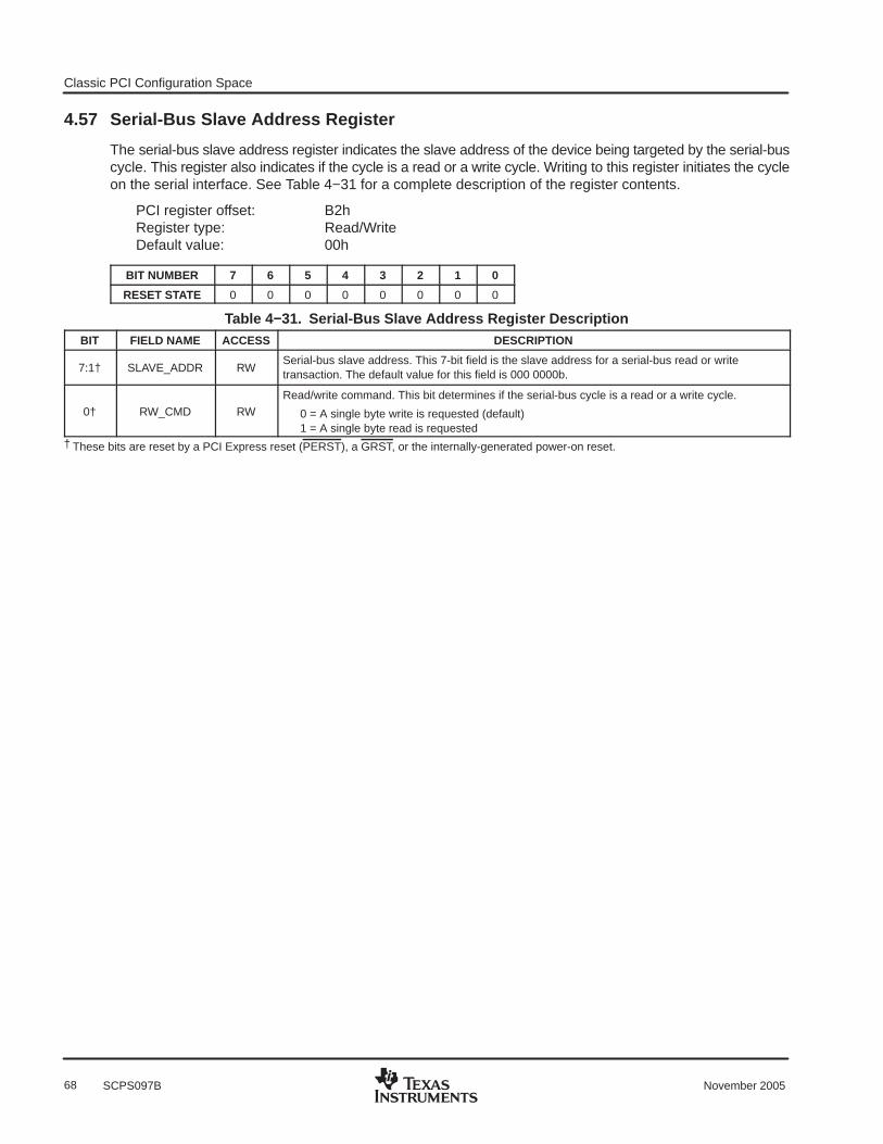
Classic PCI Configuration Space
68 November 2005SCPS097B
4.57 Serial-Bus Slave Address Register
The serial-bus slave address register indicates the slave address of the device being targeted by the serial-buscycle. This register also indicates if the cycle is a read or a write cycle. Writing to this register initiates the cycleon the serial interface. See Table 4−31 for a complete description of the register contents.
PCI register offset: B2hRegister type: Read/WriteDefault value: 00h
BIT NUMBER 7 6 5 4 3 2 1 0
RESET STATE 0 0 0 0 0 0 0 0
Table 4−31. Serial-Bus Slave Address Register DescriptionBIT FIELD NAME ACCESS DESCRIPTION
7:1† SLAVE_ADDR RWSerial-bus slave address. This 7-bit field is the slave address for a serial-bus read or writetransaction. The default value for this field is 000 0000b.
0† RW_CMD RWRead/write command. This bit determines if the serial-bus cycle is a read or a write cycle.
0 = A single byte write is requested (default)1 = A single byte read is requested
† These bits are reset by a PCI Express reset (PERST), a GRST, or the internally-generated power-on reset.

Classic PCI Configuration Space
69November 2005 SCPS097B
4.58 Serial-Bus Control and Status Register
The serial-bus control and status register controls the behavior of the serial-bus interface. This register alsoprovides status information about the state of the serial bus. See Table 4−32 for a complete description of theregister contents.
PCI register offset: B3hRegister type: Read-only, Read/Write, Read/ClearDefault value: 00h
BIT NUMBER 7 6 5 4 3 2 1 0
RESET STATE 0 0 0 0 0 0 0 0
Table 4−32. Serial-Bus Control and Status Register DescriptionBIT FIELD NAME ACCESS DESCRIPTION
7† PROT_SEL RWProtocol select. This bit selects the serial-bus address mode used.
0 = Slave address and word address are sent on the serial-bus (default)1 = Only the slave address is sent on the serial-bus
6 RSVD R Reserved. Returns 0b when read.
5† REQBUSY RU
Requested serial-bus access busy. This bit is set when a software-initiated serial-bus cycle is inprogress.
0 = No serial-bus cycle1 = Serial-bus cycle in progress
4† ROMBUSY RU
Serial EEPROM access busy. This bit is set when the serial EEPROM circuitry in the bridge isdownloading register defaults from a serial EEPROM.
0 = No EEPROM activity1 = EEPROM download in progress
3† SBDETECT RWU
Serial EEPROM detected. This bit enables the serial-bus interface. The value of this bit controlswhether the GPIO4//SCL and GPIO5//SDA terminals are configured as GPIO signals or asserial-bus signals. This bit is automatically set to 1b when a serial EEPROM is detected.
Note: A serial EEPROM is only detected once following PERST.
0 = No EEPROM present, EEPROM load process does not happen. GPIO4//SCL and GPIO5//SDA terminals are configured as GPIO signals.
1 = EEPROM present, EEPROM load process takes place. GPIO4//SCL and GPIO5//SDA terminals are configured as serial-bus signals.
2† SBTEST RW
Serial-bus test. This bit is used for internal test purposes. This bit controls the clock source for theserial interface clock.
0 = Serial-bus clock at normal operating frequency ~ 60 kHz (default)1 = Serial-bus clock frequency increased for test purposes ~ 4 MHz
1† SB_ERR RCUSerial-bus error. This bit is set when an error occurs during a software-initiated serial-bus cycle.
0 = No error1 = Serial-bus error
0† ROM_ERR RCU
Serial EEPROM load error. This bit is set when an error occurs while downloading registers from aserial EEPROM.
0 = No error1 = EEPROM load error
† These bits are reset by a PCI Express reset (PERST), a GRST, or the internally-generated power-on reset.

Classic PCI Configuration Space
70 November 2005SCPS097B
4.59 GPIO Control Register
This register controls the direction of the eight GPIO terminals. This register has no effect on the behavior ofGPIO terminals that are enabled to perform secondary functions. The secondary functions share GPIO0(CLKRUN), GPIO1 (PWR_OVRD), GPIO4 (SCL), and GPIO5 (SDA). See Table 4−33 for a completedescription of the register contents.
PCI register offset: B4hRegister type: Read-only, Read/WriteDefault value: 0000h
BIT NUMBER 15 14 13 12 11 10 9 8 7 6 5 4 3 2 1 0
RESET STATE 0 0 0 0 0 0 0 0 0 0 0 0 0 0 0 0
Table 4−33. GPIO Control Register DescriptionBIT FIELD NAME ACCESS DESCRIPTION
15:8 RSVD R Reserved. Returns 00h when read.
7† GPIO7_DIR RWGPIO 7 data direction. This bit selects whether GPIO7 is in input or output mode.
0 = Input (default)1 = Output
6† GPIO6_DIR RWGPIO 6 data direction. This bit selects whether GPIO6 is in input or output mode.
0 = Input (default)1 = Output
5† GPIO5_DIR RWGPIO 5 data direction. This bit selects whether GPIO5 is in input or output mode.
0 = Input (default)1 = Output
4† GPIO4_DIR RWGPIO 4 data direction. This bit selects whether GPIO4 is in input or output mode.
0 = Input (default)1 = Output
3† GPIO3_DIR RWGPIO 3 data direction. This bit selects whether GPIO3 is in input or output mode.
0 = Input (default)1 = Output
2† GPIO2_DIR RWGPIO 2 data direction. This bit selects whether GPIO2 is in input or output mode.
0 = Input (default)1 = Output
1† GPIO1_DIR RWGPIO 1 data direction. This bit selects whether GPIO1 is in input or output mode.
0 = Input (default)1 = Output
0† GPIO0_DIR RWGPIO 0 data direction. This bit selects whether GPIO0 is in input or output mode.
0 = Input (default)1 = Output
† These bits are reset by a PCI Express reset (PERST), a GRST, or the internally-generated power-on reset.

Classic PCI Configuration Space
71November 2005 SCPS097B
4.60 GPIO Data Register
This register reads the state of the input mode GPIO terminals and changes the state of the output mode GPIOterminals. Writing to a bit that is in input mode or is enabled for a secondary function is ignored. The secondaryfunctions share GPIO0 (CLKRUN), GPIO1 (PWR_OVRD), GPIO4 (SCL), and GPIO5 (SDA). The defaultvalue at power up depends on the state of the GPIO terminals as they default to general-purpose inputs. SeeTable 4−34 for a complete description of the register contents.
PCI register offset: B6hRegister type: Read-only, Read/WriteDefault value: 00XXh
BIT NUMBER 15 14 13 12 11 10 9 8 7 6 5 4 3 2 1 0
RESET STATE 0 0 0 0 0 0 0 0 x x x x x x x x
Table 4−34. GPIO Data Register DescriptionBIT FIELD NAME ACCESS DESCRIPTION
15:8 RSVD R Reserved. Returns 00h when read.
7† GPIO7_DATA RWGPIO 7 data. This bit reads the state of GPIO7 when in input mode or changes the state of GPIO7when in output mode.
6† GPIO6_DATA RWGPIO 6 data. This bit reads the state of GPIO6 when in input mode or changes the state of GPIO6when in output mode.
5† GPIO5_DATA RWGPIO 5 data. This bit reads the state of GPIO5 when in input mode or changes the state of GPIO5when in output mode.
4† GPIO4_DATA RWGPIO 4 data. This bit reads the state of GPIO4 when in input mode or changes the state of GPIO4when in output mode.
3† GPIO3_DATA RWGPIO 3 data. This bit reads the state of GPIO3 when in input mode or changes the state of GPIO3when in output mode.
2† GPIO2_DATA RWGPIO 2 data. This bit reads the state of GPIO2 when in input mode or changes the state of GPIO2when in output mode.
1† GPIO1_DATA RWGPIO 1 data. This bit reads the state of GPIO1 when in input mode or changes the state of GPIO1when in output mode.
0† GPIO0_DATA RWGPIO 0 data. This bit reads the state of GPIO0 when in input mode or changes the state of GPIO0when in output mode.
† These bits are reset by a PCI Express reset (PERST), a GRST, or the internally-generated power-on reset.

Classic PCI Configuration Space
72 November 2005SCPS097B
4.61 Control and Diagnostic Register 0
The contents of this register are used for monitoring status and controlling behavior of the bridge. SeeTable 4−35 for a complete description of the register contents. It is recommended that all values within thisregister be left at the default value. Improperly programming fields in this register may cause interoperabilityor other problems.
PCI register offset: C0hRegister type: Read/WriteDefault value: 0000 0000h
BIT NUMBER 31 30 29 28 27 26 25 24 23 22 21 20 19 18 17 16
RESET STATE 0 0 0 0 0 0 0 0 0 0 0 0 0 0 0 0
BIT NUMBER 15 14 13 12 11 10 9 8 7 6 5 4 3 2 1 0
RESET STATE 0 0 0 0 0 0 0 0 0 0 0 0 0 0 0 0
Table 4−35. Control and Diagnostic Register 0 DescriptionBIT FIELD NAME ACCESS DESCRIPTION
31:24† PRI_BUS_NUM R This field contains the captured primary bus number
23:19†PRI_DEVICE_
NUMR This field contains the captured primary device number
18:16 RSVD R Reserved. Returns 000b when read.
15:14† RSVD RWReserved. Bits 15:14 default to 00b. If this register is programmed via EEPROM or anothermechanism, the value written into this field must be 00b.
13:12 RSVD R Reserved. Returns 00b when read.
11:8† RSVD RWReserved. Bits 11:8 default to 0000b. If this register is programmed via EEPROM or anothermechanism, the value written into this field must be 0000b.
7 RSVD R Reserved. Returns 0b when read.
6† PREFETCH_4X RW
Prefetch 4X enable. This bit sets the prefetch behavior for upstream memory read multipletransactions. If bit 24 (FORCE_MRM) in the general control register (offset D4h, see Section 4.65)is set, then all upstream memory read transactions will prefetch the indicated number of cache lines.If bit 19 (READ_PREFETCH_DIS) in the general control register (offset D4h, see Section 4.65) isset, then this bit has no effect and only 1 DWORD will be fetched.
0 = The bridge will prefetch up to 2 cache lines, as defined in the cache line size register (offset 0Ch, see Section 4.6) for upstream memory read multiple (MRM) transactions (default)
1 = The bridge device will prefetch up to 4 cache lines, as defined in the cache line size register (offset 0Ch, see Section 4.6) for upstream memory read multiple (MRM) transactions.
5:4†UP_REQ_BUF
_VALUERW
PCI upstream req−res buffer threshold value. The value in this field controls the buffer space thatmust be available for the bridge to accept a PCI bus transaction. If the cache line size is not valid,then the bridge will use 8 DW for calculating the threshold value
00 = 1 Cacheline + 4 DW (default)01 = 1 Cacheline + 8 DW10 = 1 Cacheline + 12 DW11 = 2 Cachelines + 4 DW
3†UP_REQ_BUF
_CTRLRW
PCI upstream req-res buffer threshold control. This bit enables the PCI upstream req-res bufferthreshold control mode of the bridge.
0 = PCI upstream req-res buffer threshold control mode disabled (default)1 = PCI upstream req-res buffer threshold control mode enabled
2†CFG_ACCESS
_MEM_REGRW
Configuration access to memory-mapped registers. When this bit is set, the bridge allowsconfiguration access to memory-mapped configuration registers.
1† RSVD RWReserved. Bit 1 defaults to 0b. If this register is programmed via EEPROM or another mechanism,the value written into this field must be 0b.
0 RSVD R Reserved. Returns 0b when read.
† These bits are reset by a PCI Express reset (PERST), a GRST, or the internally-generated power-on reset.
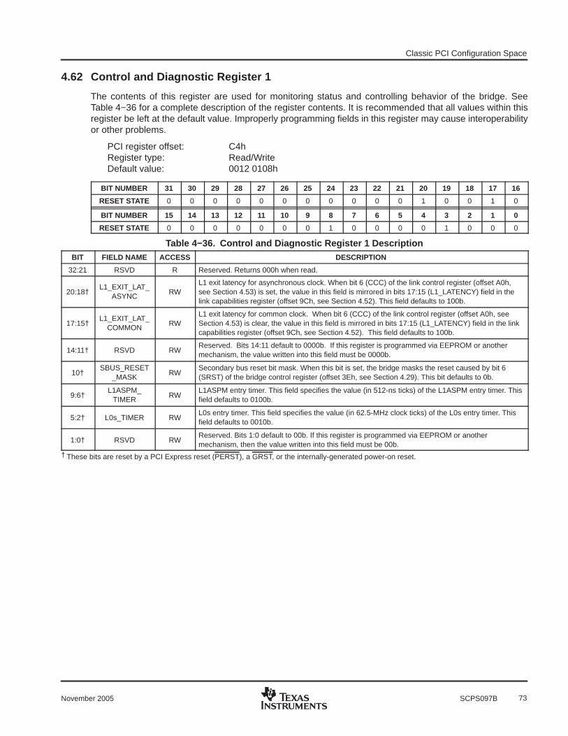
Classic PCI Configuration Space
73November 2005 SCPS097B
4.62 Control and Diagnostic Register 1
The contents of this register are used for monitoring status and controlling behavior of the bridge. SeeTable 4−36 for a complete description of the register contents. It is recommended that all values within thisregister be left at the default value. Improperly programming fields in this register may cause interoperabilityor other problems.
PCI register offset: C4hRegister type: Read/WriteDefault value: 0012 0108h
BIT NUMBER 31 30 29 28 27 26 25 24 23 22 21 20 19 18 17 16
RESET STATE 0 0 0 0 0 0 0 0 0 0 0 1 0 0 1 0
BIT NUMBER 15 14 13 12 11 10 9 8 7 6 5 4 3 2 1 0
RESET STATE 0 0 0 0 0 0 0 1 0 0 0 0 1 0 0 0
Table 4−36. Control and Diagnostic Register 1 DescriptionBIT FIELD NAME ACCESS DESCRIPTION
32:21 RSVD R Reserved. Returns 000h when read.
20:18†L1_EXIT_LAT_
ASYNCRW
L1 exit latency for asynchronous clock. When bit 6 (CCC) of the link control register (offset A0h,see Section 4.53) is set, the value in this field is mirrored in bits 17:15 (L1_LATENCY) field in thelink capabilities register (offset 9Ch, see Section 4.52). This field defaults to 100b.
17:15†L1_EXIT_LAT_
COMMONRW
L1 exit latency for common clock. When bit 6 (CCC) of the link control register (offset A0h, seeSection 4.53) is clear, the value in this field is mirrored in bits 17:15 (L1_LATENCY) field in the linkcapabilities register (offset 9Ch, see Section 4.52). This field defaults to 100b.
14:11† RSVD RWReserved. Bits 14:11 default to 0000b. If this register is programmed via EEPROM or anothermechanism, the value written into this field must be 0000b.
10†SBUS_RESET
_MASKRW
Secondary bus reset bit mask. When this bit is set, the bridge masks the reset caused by bit 6(SRST) of the bridge control register (offset 3Eh, see Section 4.29). This bit defaults to 0b.
9:6†L1ASPM_
TIMERRW
L1ASPM entry timer. This field specifies the value (in 512-ns ticks) of the L1ASPM entry timer. Thisfield defaults to 0100b.
5:2† L0s_TIMER RWL0s entry timer. This field specifies the value (in 62.5-MHz clock ticks) of the L0s entry timer. Thisfield defaults to 0010b.
1:0† RSVD RWReserved. Bits 1:0 default to 00b. If this register is programmed via EEPROM or anothermechanism, then the value written into this field must be 00b.
† These bits are reset by a PCI Express reset (PERST), a GRST, or the internally-generated power-on reset.

Classic PCI Configuration Space
74 November 2005SCPS097B
4.63 Control and Diagnostic Register 2
The contents of this register are used for monitoring status and controlling behavior of the bridge. SeeTable 4−37 for a complete description of the register contents. It is recommended that all values within thisregister be left at the default value. Improperly programming fields in this register may cause interoperabilityor other problems.
PCI register offset: C8hRegister type: Read/WriteDefault value: 3214 6000h
BIT NUMBER 31 30 29 28 27 26 25 24 23 22 21 20 19 18 17 16
RESET STATE 0 0 1 1 0 0 1 0 0 0 0 1 0 1 0 0
BIT NUMBER 15 14 13 12 11 10 9 8 7 6 5 4 3 2 1 0
RESET STATE 0 1 1 0 0 0 0 0 0 0 0 0 0 0 0 0
Table 4−37. Control and Diagnostic Register 2 DescriptionBIT FIELD NAME ACCESS DESCRIPTION
31:24†N_FTS_
ASYNC_CLKRW
N_FTS for asynchronous clock. When bit 6 (CCC) of the link control register (offset A0h, seeSection 4.53) is clear, the value in this field is the number of FTS that are sent on a transition fromL0s to L0. This field shall default to 32h.
23:16†N_FTS_
COMMON_CLK
RWN_FTS for common clock. When bit 6 (CCC) of the link control register (offset A0h, see Section4.53) is set, the value in this field is the number of FTS that are sent on a transition from L0s to L0.This field defaults to 14h.
15:13 PHY_REV R PHY revision number
12:8† LINK_NUM RW Link number
7:6 RSVD R Reserved. Returns 00b when read.
5:0† RSVD RWReserved. Bits 5:0 default to 000000b. If this register is programmed via EEPROM or anothermechanism, then the value written into this field must be 000000b.
† These bits are reset by a PCI Express reset (PERST), a GRST, or the internally-generated power-on reset.
4.64 Subsystem Access Register
The contents of this read/write register are aliased to the subsystem vendor ID and subsystem ID registersat PCI offsets 84h and 86h. See Table 4−38 for a complete description of the register contents.
PCI register offset: D0hRegister type: Read/WriteDefault value: 0000 0000h
BIT NUMBER 31 30 29 28 27 26 25 24 23 22 21 20 19 18 17 16
RESET STATE 0 0 0 0 0 0 0 0 0 0 0 0 0 0 0 0
BIT NUMBER 15 14 13 12 11 10 9 8 7 6 5 4 3 2 1 0
RESET STATE 0 0 0 0 0 0 0 0 0 0 0 0 0 0 0 0
Table 4−38. Subsystem Access Register DescriptionBIT FIELD NAME ACCESS DESCRIPTION
31:16† SubsystemID RWSubsystem ID. The value written to this field is aliased to the subsystem ID register at PCIoffset 86h (see Section 4.45).
15:0† SubsystemVendorID RWSubsystem vendor ID. The value written to this field is aliased to the subsystem vendor IDregister at PCI offset 84h (see Section 4.44).
† These bits are reset by a PCI Express reset (PERST), a GRST, or the internally-generated power-on reset.

Classic PCI Configuration Space
75November 2005 SCPS097B
4.65 General Control RegisterThis read/write register controls various functions of the bridge. See Table 4−39 for a complete descriptionof the register contents.
PCI register offset: D4hRegister type: Read-only, Read/WriteDefault value: 8206 C000h
BIT NUMBER 31 30 29 28 27 26 25 24 23 22 21 20 19 18 17 16
RESET STATE 1 0 0 0 0 0 1 0 0 0 0 0 0 1 1 0
BIT NUMBER 15 14 13 12 11 10 9 8 7 6 5 4 3 2 1 0
RESET STATE 1 1 0 0 0 0 0 0 0 0 0 0 0 0 0 0
Table 4−39. General Control Register DescriptionBIT FIELD NAME ACCESS DESCRIPTION
31:30†CFG_RETRY
_CNTRRW
Configuration retry counter. Configures the amount of time that a configuration request must be retriedon the secondary PCI bus before it may be completed with configuration retry status on the PCIExpress side.
00 = 25 µs01 = 1 ms10 = 25 ms (default)11 = 50 ms
29:28 RSVD R Reserved. Returns 00b when read.
27†LOW_POWER
_ENRW
Low-power enable. When this bit is set, the half-ampitude, no preemphasis mode for the PCI ExpressTX drivers is enabled. The default for this bit is 0b.
26†PCI_PM_
VERSION_CTRL
RW
PCI power management version control. This bit controls the value reported in bits 2:0 (PM_VERSION)in the power management capabilities register (offset 52h, see Section 4.32). It also controls the valueof bit 3 (NO_SOFT_RESET) in the power management control/status register (offset 54h, see Section4.33).
0 = Version fields reports 010b and NO_SOFT_RESET reports 0b for Power Management 1.1 compliance (default)
1 = Version fields reports 011b and NO_SOFT_RESET reports 1b for Power Management 1.2 compliance
25†STRICT_
PRIORITY_ENRW
Strict priority enable. When this bit is set and bits 6:4 (LOW_PRIORITY_COUNT) in the port VCcapability register 1 (offset 154h, see Section 5.17) are 000b, meaning that strict priority VC arbitrationis used, the extended VC always receives priority over VC0 at the PCI Express port.
0 = The default LOW_PRIORITY_COUNT is 001b 1 = The default LOW_PRIORITY_COUNT is 000b (default)
24† FORCE_MRM RW
Force memory read multiple0 = Memory read multiple transactions are disabled (default)1 = All upstream memory read transactions initiated on the PCI bus are treated as though they
are memory read multiple transactions where prefetching is supported
23†ASPM_CTRL_DEF_OVRD
RW
Active state power management control default override. This bit determines the power-up default forbits 1:0 (ASLPMC) of the link control register (offset A0h, see Section 4.53) in the PCI Expresscapability structure.
0 = Power-on default indicates that active state power management is disabled (00b) (default)1 = Power-on default indicates that active state power management is enabled for L0s and L1 (11b)
22:20†POWER_
OVRDRW
Power override. This bit field determines how the bridge responds when the slot power limit is lessthan the amount of power required by the bridge and the devices behind the bridge.
000 = Ignore slot power limit (default)001 = Assert the PWR_OVRD terminal010 = Disable secondary clocks selected by the clock mask register011 = Disable secondary clocks selected by the clock mask register and assert the PWR_OVRD
terminal100 = Respond with unsupported request to all transactions except for configuration transactions
(type 0 or type 1) and set slot power limit messages101, 110, 111 = Reserved
† These bits are reset by a PCI Express reset (PERST), a GRST, or the internally-generated power-on reset.

Classic PCI Configuration Space
76 November 2005SCPS097B
Table 4−39. General Control Register Description (Continued)
BIT FIELD NAME ACCESS DESCRIPTION
19†READ_
PREFETCH_DIS
RWRead prefetch disable. This bit controls the prefetch functionality on PCI memory read transactions.
0 = Prefetch to the next cache line boundary on a burst read (default)1 = Fetch only a single DWORD on a burst read
18:16† L0s_LATENCY RW
L0s maximum exit latency. This field programs the maximum acceptable latency when exiting the L0sstate. This sets bits 8:6 (EP_L0S_LAT) in the device capabilities register (offset 94h, see Section4.49).
000 = Less than 64 ns001 = 64 ns up to less than 128 ns010 = 128 ns up to less than 256 ns011 = 256 ns up to less than 512 ns100 = 512 ns up to less than 1 µs101 = 1 µs up to less than 2 µs110 = 2 µs to 4 µs (default)111 = More than 4 µs
15:13† L1_LATENCY RW
L1 maximum exit latency. This field programs the maximum acceptable latency when exiting the L1state. This sets bits 11:9 (EP_L1_LAT) in the device capabilities register (offset 94h, seeSection 4.49).
000 = Less than 1 µs001 = 1 µs up to less than 2 µs010 = 2 µs up to less than 4 µs011 = 4 µs up to less than 8 µs100 = 8 µs up to less than 16 µs101 = 16 µs up to less than 32 µs110 = 32 µs to 64 µs (default)111 = More than 64 µs
12† VC_CAP_EN RW
VC capability structure enable. This bit enables the VC capability structure by changing the nextoffset field of the advanced error reporting capability register at offset 102h.
0 = VC capability structure disabled (offset field = 000h) 1 = VC capability structure enabled (offset field = 150h)
11 BPCC_E RW
Bus power clock control enable. This bit controls whether the secondary bus PCI clocks are stoppedwhen the bridge is placed in the D3 state. It is assumed that if the secondary bus clocks are requiredto be active, that a reference clock continues to be provided on the PCI Express interface.
0 = Secondary bus clocks are not stopped in D3 (default)1 = Secondary bus clocks are stopped on D3
10BEACON_ENABLE
RW
Beacon enable. This bit controls the mechanism for waking up the physical PCI Express link when inL2.
0 = WAKE mechanism is used exclusively. Beacon is not used (default).1 = Beacon and WAKE mechanisms are used
9:8†MIN_POWER_
SCALERW
Minimum power scale. This value is programmed to indicate the scale of bits 7:0(MIN_POWER_VALUE).
00 = 1.0x (default)01 = 0.1x10 = 0.01x11 = 0.001x
7:0†MIN_POWER_
VALUERW
Minimum power value. This value is programmed to indicate the minimum power requirements. Thisvalue is multiplied by the minimum power scale field (bits 9:8) to determine the minimum powerrequirements for the bridge. The default is 00h, because this feature is only usable when the systemimplementer adds the PCI devices’ power consumption to the bridge power consumption andreprograms this field with an EEPROM or the system BIOS.
† These bits are reset by a PCI Express reset (PERST), a GRST, or the internally-generated power-on reset.
These bits are sticky and must retain their value when the bridge is powered by VAUX.

Classic PCI Configuration Space
77November 2005 SCPS097B
4.66 Clock Control Register
This register enables and disables the PCI clock outputs (CLKOUT). See Table 4−40 for a completedescription of the register contents.
PCI register offset: D8hRegister type: Read-only, Read/WriteDefault value: 00h
BIT NUMBER 7 6 5 4 3 2 1 0
RESET STATE 0 0 0 0 0 0 0 0
Table 4−40. Clock Control Register DescriptionBIT FIELD NAME ACCESS DESCRIPTION
7 RSVD R Reserved. Returns 0b when read.
6† CLOCK6_DISABLE RWClock output 6 disable. This bit disables secondary CLKOUT6.
0 = Clock enabled (default)1 = Clock disabled
5† CLOCK5_DISABLE RWClock output 5 disable. This bit disables secondary CLKOUT5.
0 = Clock enabled (default)1 = Clock disabled
4† CLOCK4_DISABLE RWClock output 4 disable. This bit disables secondary CLKOUT4.
0 = Clock enabled (default)1 = Clock disabled
3† CLOCK3_DISABLE RWClock output 3 disable. This bit disables secondary CLKOUT3.
0 = Clock enabled (default)1 = Clock disabled
2† CLOCK2_DISABLE RWClock output 2 disable. This bit disables secondary CLKOUT2.
0 = Clock enabled (default)1 = Clock disabled
1† CLOCK1_DISABLE RWClock output 1 disable. This bit disables secondary CLKOUT1.
0 = Clock enabled (default)1 = Clock disabled
0† CLOCK0_DISABLE RWClock output 0 disable. This bit disables secondary CLKOUT0.
0 = Clock enabled (default)1 = Clock disabled
† These bits are reset by a PCI Express reset (PERST), a GRST, or the internally-generated power-on reset.

Classic PCI Configuration Space
78 November 2005SCPS097B
4.67 Clock Mask Register
This register selects which PCI bus clocks are disabled when bits 22:20 (POWER_OVRD) in the generalcontrol register (offset D4h, see Section 4.65) are set to 010h or 011h. This register has no effect on the clockoutputs if the POWER_OVRD bits are not set to 010h or 011h or if the slot power limit is greater than the powerrequired. See Table 4−41 for a complete description of the register contents.
PCI register offset: D9hRegister type: Read-only, Read/WriteDefault value: 00h
BIT NUMBER 7 6 5 4 3 2 1 0
RESET STATE 0 0 0 0 0 0 0 0
Table 4−41. Clock Mask Register DescriptionBIT FIELD NAME ACCESS DESCRIPTION7 RSVD R Reserved. Returns 0b when read.
6† CLOCK6_MASK RW
Clock output 6 mask. This bit disables PCI bus CLKOUT6 when the POWER_OVRD bits are setto 010b or 011b and the slot power limit is exceeded.
0 = Clock enabled (default)1 = Clock disabled
5† CLOCK5_MASK RW
Clock output 5 mask. This bit disables PCI bus CLKOUT5 when the POWER_OVRD bits are setto 010b or 011b and the slot power limit is exceeded.
0 = Clock enabled (default)1 = Clock disabled
4† CLOCK4_MASK RW
Clock output 4 mask. This bit disables PCI bus CLKOUT4 when the POWER_OVRD bits are setto 010b or 011b and the slot power limit is exceeded.
0 = Clock enabled (default)1 = Clock disabled
3† CLOCK3_MASK RW
Clock output 3 mask. This bit disables PCI bus CLKOUT3 when the POWER_OVRD bits are setto 010b or 011b and the slot power limit is exceeded.
0 = Clock enabled (default)1 = Clock disabled
2† CLOCK2_MASK RW
Clock output 2 mask. This bit disables PCI bus CLKOUT2 when the POWER_OVRD bits are setto 010b or 011b and the slot power limit is exceeded.
0 = Clock enabled (default)1 = Clock disabled
1† CLOCK1_MASK RW
Clock output 1 mask. This bit disables PCI bus CLKOUT1 when the POWER_OVRD bits are setto 010b or 011b and the slot power limit is exceeded.
0 = Clock enabled (default)1 = Clock disabled
0† CLOCK0_MASK RW
Clock output 0 mask. This bit disables PCI bus CLKOUT0 when the POWER_OVRD bits are setto 010b or 011b and the slot power limit is exceeded.
0 = Clock enabled (default)1 = Clock disabled
† These bits are reset by a PCI Express reset (PERST), a GRST, or the internally-generated power-on reset.

Classic PCI Configuration Space
79November 2005 SCPS097B
4.68 Clock Run Status Register
The clock run status register indicates the state of the PCI clock-run features in the bridge. See Table 4−42for a complete description of the register contents.
PCI register offset: DAhRegister type: Read-onlyDefault value: 00h
BIT NUMBER 7 6 5 4 3 2 1 0
RESET STATE 0 0 0 0 0 0 0 0
Table 4−42. Clock Run Status Register DescriptionBIT FIELD NAME ACCESS DESCRIPTION
7:1 RSVD R Reserved. Returns 000 0000b when read.
0† SEC_CLK_STATUS RUSecondary clock status. This bit indicates the status of the PCI bus secondary clock outputs.
0 = Secondary clock running1 = Secondary clock stopped
† This bit is reset by a PCI Express reset (PERST), a GRST, or the internally-generated power-on reset.
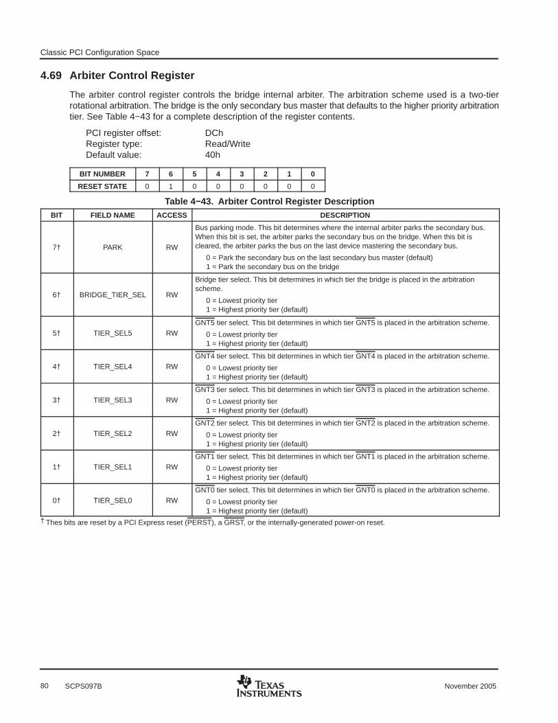
Classic PCI Configuration Space
80 November 2005SCPS097B
4.69 Arbiter Control Register
The arbiter control register controls the bridge internal arbiter. The arbitration scheme used is a two-tierrotational arbitration. The bridge is the only secondary bus master that defaults to the higher priority arbitrationtier. See Table 4−43 for a complete description of the register contents.
PCI register offset: DChRegister type: Read/WriteDefault value: 40h
BIT NUMBER 7 6 5 4 3 2 1 0
RESET STATE 0 1 0 0 0 0 0 0
Table 4−43. Arbiter Control Register DescriptionBIT FIELD NAME ACCESS DESCRIPTION
7† PARK RW
Bus parking mode. This bit determines where the internal arbiter parks the secondary bus.When this bit is set, the arbiter parks the secondary bus on the bridge. When this bit iscleared, the arbiter parks the bus on the last device mastering the secondary bus.
0 = Park the secondary bus on the last secondary bus master (default) 1 = Park the secondary bus on the bridge
6† BRIDGE_TIER_SEL RW
Bridge tier select. This bit determines in which tier the bridge is placed in the arbitrationscheme.
0 = Lowest priority tier1 = Highest priority tier (default)
5† TIER_SEL5 RWGNT5 tier select. This bit determines in which tier GNT5 is placed in the arbitration scheme.
0 = Lowest priority tier1 = Highest priority tier (default)
4† TIER_SEL4 RWGNT4 tier select. This bit determines in which tier GNT4 is placed in the arbitration scheme.
0 = Lowest priority tier1 = Highest priority tier (default)
3† TIER_SEL3 RWGNT3 tier select. This bit determines in which tier GNT3 is placed in the arbitration scheme.
0 = Lowest priority tier1 = Highest priority tier (default)
2† TIER_SEL2 RWGNT2 tier select. This bit determines in which tier GNT2 is placed in the arbitration scheme.
0 = Lowest priority tier1 = Highest priority tier (default)
1† TIER_SEL1 RWGNT1 tier select. This bit determines in which tier GNT1 is placed in the arbitration scheme.
0 = Lowest priority tier1 = Highest priority tier (default)
0† TIER_SEL0 RWGNT0 tier select. This bit determines in which tier GNT0 is placed in the arbitration scheme.
0 = Lowest priority tier1 = Highest priority tier (default)
† Thes bits are reset by a PCI Express reset (PERST), a GRST, or the internally-generated power-on reset.

Classic PCI Configuration Space
81November 2005 SCPS097B
4.70 Arbiter Request Mask Register
The arbiter request mask register enables and disables support for requests from specific masters on thesecondary bus. The arbiter request mask register also controls if a request input is automatically masked onan arbiter time-out. See Table 4−44 for a complete description of the register contents.
PCI register offset: DDhRegister type: Read/WriteDefault value: 00h
BIT NUMBER 7 6 5 4 3 2 1 0
RESET STATE 0 0 0 0 0 0 0 0
Table 4−44. Arbiter Request Mask Register DescriptionBIT FIELD NAME ACCESS DESCRIPTION
7† ARB_TIMEOUT RW
Arbiter time-out. This bit enables the arbiter time-out feature. The arbiter time-out is defined asthe number of PCI clocks after the PCI bus has gone idle for a device to assert FRAME beforethe arbiter assumes the device will not respond.
0 = Arbiter time disabled (default)1 = Arbiter time-out set to 16 PCI clocks
6† AUTO_MASK RW
Automatic request mask. This bit enables automatic request masking when an arbiter time-outoccurs.
0 = Automatic request masking disabled (default)1 = Automatic request masking enabled
5† REQ5_MASK RW
Request 5 (REQ5) mask. Setting this bit forces the internal arbiter to ignore requests signal onrequest input 5.
0 = Use request 5 (default)1 = Ignore request 5
4† REQ4_MASK RW
Request 4 (REQ4) mask. Setting this bit forces the internal arbiter to ignore requests signal onrequest input 4.
0 = Use request 4 (default)1 = Ignore request 4
3† REQ3_MASK RW
Request 3 (REQ3) mask. Setting this bit forces the internal arbiter to ignore requests signal onrequest input 3.
0 = Use request 3 (default)1 = Ignore request 3
2† REQ2_MASK RW
Request 2 (REQ2) mask. Setting this bit forces the internal arbiter to ignore requests signal onrequest input 2.
0 = Use request 2 (default)1 = Ignore request 2
1† REQ1_MASK RW
Request 1 (REQ1) mask. Setting this bit forces the internal arbiter to ignore requests signal onrequest input 1.
0 = Use request 1 (default)1 = Ignore request 1
0† REQ0_MASK RW
Request 0 (REQ0) mask. Setting this bit forces the internal arbiter to ignore requests signal onrequest input 0.
0 = Use request 0 (default)1 = Ignore request 0
† These bits are reset by a PCI Express reset (PERST), a GRST, or the internally-generated power-on reset.
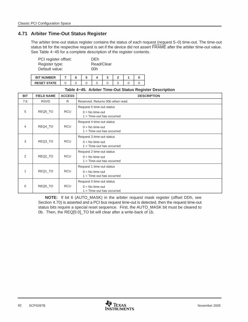
Classic PCI Configuration Space
82 November 2005SCPS097B
4.71 Arbiter Time-Out Status Register
The arbiter time-out status register contains the status of each request (request 5–0) time-out. The time-outstatus bit for the respective request is set if the device did not assert FRAME after the arbiter time-out value.See Table 4−45 for a complete description of the register contents.
PCI register offset: DEhRegister type: Read/ClearDefault value: 00h
BIT NUMBER 7 6 5 4 3 2 1 0
RESET STATE 0 0 0 0 0 0 0 0
Table 4−45. Arbiter Time-Out Status Register DescriptionBIT FIELD NAME ACCESS DESCRIPTION
7:6 RSVD R Reserved. Returns 00b when read.
5 REQ5_TO RCURequest 5 time-out status
0 = No time-out 1 = Time-out has occurred
4 REQ4_TO RCURequest 4 time-out status
0 = No time-out 1 = Time-out has occurred
3 REQ3_TO RCURequest 3 time-out status
0 = No time-out 1 = Time-out has occurred
2 REQ2_TO RCURequest 2 time-out status
0 = No time-out 1 = Time-out has occurred
1 REQ1_TO RCURequest 1 time-out status
0 = No time-out 1 = Time-out has occurred
0 REQ0_TO RCURequest 0 time-out status
0 = No time-out 1 = Time-out has occurred
NOTE: If bit 6 (AUTO_MASK) in the arbiter request mask register (offset DDh, seeSection 4.70) is asserted and a PCI bus request time-out is detected, then the request time-outstatus bits require a special reset sequence. First, the AUTO_MASK bit must be cleared to0b. Then, the REQ[5:0]_TO bit will clear after a write-back of 1b.

Classic PCI Configuration Space
83November 2005 SCPS097B
4.72 Serial IRQ Mode Control Register
This register controls the behavior of the serial IRQ controller. See Table 4−46 for a complete description ofthe register contents.
PCI register offset: E0hRegister type: Read-only, Read/WriteDefault value: 00h
BIT NUMBER 7 6 5 4 3 2 1 0
RESET STATE 0 0 0 0 0 0 0 0
Table 4−46. Serial IRQ Mode Control Register DescriptionBIT FIELD NAME ACCESS DESCRIPTION
7:4 RSVD R Reserved. Returns 0h when read.
3:2† START_WIDTH RW
Start frame pulse width. Sets the width of the start frame for a SERIRQ stream.
00 = 4 clocks (default)01 = 6 clocks10 = 8 clocks11 = Reserved
1† POLLMODE RWPoll mode. This bit selects between continuous and quiet mode.
0 = Continuous mode (default)1 = Quiet mode
0† DRIVEMODE RWDrive mode. This bit selects the behavior of the serial IRQ controller during the recovery cycle.
0 = Drive high (default)1 = 3-state
† These bits are reset by a PCI Express reset (PERST), a GRST, or the internally-generated power-on reset.

Classic PCI Configuration Space
84 November 2005SCPS097B
4.73 Serial IRQ Edge Control Register
This register controls the edge mode or level mode for each IRQ in the serial IRQ stream. See Table 4−47 fora complete description of the register contents.
PCI register offset: E2hRegister type: Read/WriteDefault value: 0000h
BIT NUMBER 15 14 13 12 11 10 9 8 7 6 5 4 3 2 1 0
RESET STATE 0 0 0 0 0 0 0 0 0 0 0 0 0 0 0 0
Table 4−47. Serial IRQ Edge Control Register DescriptionBIT FIELD NAME ACCESS DESCRIPTION
15† IRQ15_MODE RWIRQ 15 edge mode
0 = Edge mode (default)1 = Level mode
14† IRQ14_MODE RWIRQ 14 edge mode
0 = Edge mode (default)1 = Level mode
13† IRQ13_MODE RWIRQ 13 edge mode
0 = Edge mode (default)1 = Level mode
12† IRQ12_MODE RWIRQ 12 edge mode
0 = Edge mode (default)1 = Level mode
11† IRQ11_MODE RWIRQ 11 edge mode
0 = Edge mode (default)1 = Level mode
10† IRQ10_MODE RWIRQ 10 edge mode
0 = Edge mode (default)1 = Level mode
9† IRQ9_MODE RWIRQ 9 edge mode
0 = Edge mode (default)1 = Level mode
8† IRQ8_MODE RWIRQ 8 edge mode
0 = Edge mode (default)1 = Level mode
7† IRQ7_MODE RWIRQ 7 edge mode
0 = Edge mode (default)1 = Level mode
6† IRQ6_MODE RWIRQ 6 edge mode
0 = Edge mode (default)1 = Level mode
5† IRQ5_MODE RWIRQ 5 edge mode
0 = Edge mode (default)1 = Level mode
4† IRQ4_MODE RWIRQ 4 edge mode
0 = Edge mode (default)1 = Level mode
3† IRQ3_MODE RWIRQ 3 edge mode
0 = Edge mode (default)1 = Level mode
2† IRQ2_MODE RWIRQ 2 edge mode
0 = Edge mode (default)1 = Level mode
† These bits are reset by a PCI Express reset (PERST), a GRST, or the internally-generated power-on reset.

Classic PCI Configuration Space
85November 2005 SCPS097B
Table 4−47. Serial IRQ Edge Control Register Description (Continued)BIT FIELD NAME ACCESS DESCRIPTION
1† IRQ1_MODE RWIRQ 1 edge mode
0 = Edge mode (default)1 = Level mode
0† IRQ0_MODE RWIRQ 0 edge mode
0 = Edge mode (default)1 = Level mode
† These bits are reset by a PCI Express reset (PERST), a GRST, or the internally-generated power-on reset.
4.74 Serial IRQ Status Register
This register indicates when a level mode IRQ is signaled on the serial IRQ stream. After a level mode IRQis signaled, a write-back of 1b to the asserted IRQ status bit re-arms the interrupt. IRQ interrupts that aredefined as edge mode in the serial IRQ edge control register are not reported in this status register. SeeTable 4−48 for a complete description of the register contents.
PCI register offset: E4hRegister type: Read/ClearDefault value: 0000h
BIT NUMBER 15 14 13 12 11 10 9 8 7 6 5 4 3 2 1 0
RESET STATE 0 0 0 0 0 0 0 0 0 0 0 0 0 0 0 0
Table 4−48. Serial IRQ Status Register DescriptionBIT FIELD NAME ACCESS DESCRIPTION
15 IRQ15 RCUIRQ 15 asserted. This bit indicates that the IRQ15 has been asserted.
0 = Deasserted1 = Asserted
14 IRQ14 RCUIRQ 14 asserted. This bit indicates that the IRQ14 has been asserted.
0 = Deasserted1 = Asserted
13 IRQ13 RCUIRQ 13 asserted. This bit indicates that the IRQ13 has been asserted.
0 = Deasserted1 = Asserted
12 IRQ12 RCUIRQ 12 asserted. This bit indicates that the IRQ12 has been asserted.
0 = Deasserted1 = Asserted
11 IRQ11 RCUIRQ 11 asserted. This bit indicates that the IRQ11 has been asserted.
0 = Deasserted1 = Asserted
10 IRQ10 RCUIRQ 10 asserted. This bit indicates that the IRQ10 has been asserted.
0 = Deasserted1 = Asserted
9 IRQ9 RCUIRQ 9 asserted. This bit indicates that the IRQ9 has been asserted.
0 = Deasserted1 = Asserted
8 IRQ8 RCUIRQ 8 asserted. This bit indicates that the IRQ8 has been asserted.
0 = Deasserted1 = Asserted
7 IRQ7 RCUIRQ 7 asserted. This bit indicates that the IRQ7 has been asserted.
0 = Deasserted1 = Asserted

Classic PCI Configuration Space
86 November 2005SCPS097B
Table 4−48. Serial IRQ Status Register Description (Continued)BIT FIELD NAME ACCESS DESCRIPTION
6 IRQ6 RCUIRQ 6 asserted. This bit indicates that the IRQ6 has been asserted.
0 = Deasserted1 = Asserted
5 IRQ5 RCUIRQ 5 asserted. This bit indicates that the IRQ5 has been asserted.
0 = Deasserted1 = Asserted
4 IRQ4 RCUIRQ 4 asserted. This bit indicates that the IRQ4 has been asserted.
0 = Deasserted1 = Asserted
3 IRQ3 RCUIRQ 3 asserted. This bit indicates that the IRQ3 has been asserted.
0 = Deasserted1 = Asserted
2 IRQ2 RCUIRQ 2 asserted. This bit indicates that the IRQ2 has been asserted.
0 = Deasserted1 = Asserted
1 IRQ1 RCUIRQ 1 asserted. This bit indicates that the IRQ1 has been asserted.
0 = Deasserted1 = Asserted
0 IRQ0 RCUIRQ 0 asserted. This bit indicates that the IRQ0 has been asserted.
0 = Deasserted1 = Asserted

PCI Express Extended Configuration Space
87November 2005 SCPS097B
5 PCI Express Extended Configuration SpaceThe programming model of the PCI Express extended configuration space is compliant to the PCI ExpressBase Specification and the PCI Express to PCI/PCI-X Bridge Specification programming models. The PCIExpress extended configuration map uses the PCI Express advanced error reporting capability and PCIExpress virtual channel (VC) capability headers.
All bits marked with a are sticky bits and are reset by a global reset (GRST) or the internally-generatedpower-on reset. All bits marked with a † are reset by a PCI Express reset (PERST), a GRST, or theinternally-generated power-on reset. The remaining register bits are reset by a PCI Express hot reset, PERST,GRST, or the internally-generated power-on reset.
Table 5−1. PCI Express Extended Configuration Register MapREGISTER NAME OFFSET
Next capability offset / capability version PCI Express advanced error reporting capabilities ID 100h
Uncorrectable error status register† 104h
Uncorrectable error mask register† 108h
Uncorrectable error severity register† 10Ch
Correctable error status register† 110h
Correctable error mask† 114h
Advanced error capabilities and control† 118h
Header log register† 11Ch
Header log register† 120h
Header log register† 124h
Header log register† 128h
Secondary uncorrectable error status† 12Ch
Secondary uncorrectable error mask† 130h
Secondary uncorrectable error severity register† 134h
Secondary error capabilities and control register† 138h
Secondary header log register† 13Ch
Secondary header log register† 140h
Secondary header log register† 144h
Secondary header log register† 148h
Reserved 14Ch
Next capability offset / capability version PCI express virtual channel extended capabilities ID 150h
Port VC capability register 1 154h
Port VC capability register 2 158h
Port VC status register Port VC control register 15Ch
VC resource capability register (VC0) 160h
VC resource control register (VC0) 164h
VC resource status register (VC0) Reserved 168h
VC resource capability register (VC1) 16Ch
VC resource control register (VC1) 170h
VC resource status register (VC1) Reserved 174h
Reserved 178h – 17Ch
VC arbitration table (phase 7 − phase 0) 180h
VC arbitration table (phase 15 − phase 8) 184h
VC arbitration table (phase 23 − phase 16) 188h† These bits are reset by a PCI Express reset (PERST), a GRST, or the internally-generated power-on reset.

PCI Express Extended Configuration Space
88 November 2005SCPS097B
Table 5−1. PCI Express Extended Configuration Register Map (Continued)REGISTER NAME OFFSET
VC arbitration table (phase 31 − phase 24) 18Ch
Reserved 190h – 1BCh
Port arbitration table for VC1 (phase 7 – phase 0) 1C0h
Port arbitration table for VC1 (phase 15 – phase 8) 1C4h
Port arbitration table for VC1 (phase 23 – phase 16) 1C8h
Port arbitration table for VC1 (phase 31 – phase 24) 1CCh
Port arbitration table for VC1 (phase 39 – phase 32) 1D0h
Port arbitration table for VC1 (phase 47 – phase 40) 1D4h
Port arbitration table for VC1 (phase 55 – phase 48) 1D8h
Port arbitration table for VC1 (phase 63 – phase 56) 1DCh
Port arbitration table for VC1 (phase 71 – phase 64) 1E0h
Port arbitration table for VC1 (phase 79 – phase 72) 1E4h
Port arbitration table for VC1 (phase 87 – phase 80) 1E8h
Port arbitration table for VC1 (phase 95 – phase 88) 1ECh
Port arbitration table for VC1 (phase 103 – phase 96) 1F0h
Port arbitration table for VC1 (phase 111 – phase 104) 1F4h
Port arbitration table for VC1 (phase 119 – phase 112) 1F8h
Port arbitration table for VC1 (phase 127 – phase 120) 1FCh
Reserved 200h – FFCh
5.1 Advanced Error Reporting Capability ID Register
This read-only register identifies the linked list item as the register for PCI Express advanced error reportingcapabilities. The register returns 0001h when read.
PCI Express extended register offset: 100hRegister type: Read-onlyDefault value: 0001h
BIT NUMBER 15 14 13 12 11 10 9 8 7 6 5 4 3 2 1 0
RESET STATE 0 0 0 0 0 0 0 0 0 0 0 0 0 0 0 1
5.2 Next Capability Offset/Capability Version Register
This read-only register identifies the next location in the PCI Express extended capabilities link list. If bit 12(VC_CAP_EN) in the general control register (offset D4h, see Section 4.65) is 0b, then the upper 12 bits inthis register are 000h, indicating the end of the linked list. If VC_CAP_EN is 1b, then the upper 12 bits in thisregister are 150h, indicating the existance of the VC capability structure at offset 150h. The four leastsignificant bits identify the revision of the current capability block as 1h.
PCI Express extended register offset: 102hRegister type: Read-onlyDefault value: XX01h
BIT NUMBER 15 14 13 12 11 10 9 8 7 6 5 4 3 2 1 0
RESET STATE 0 0 0 x 0 x 0 x 0 0 0 0 0 0 0 1
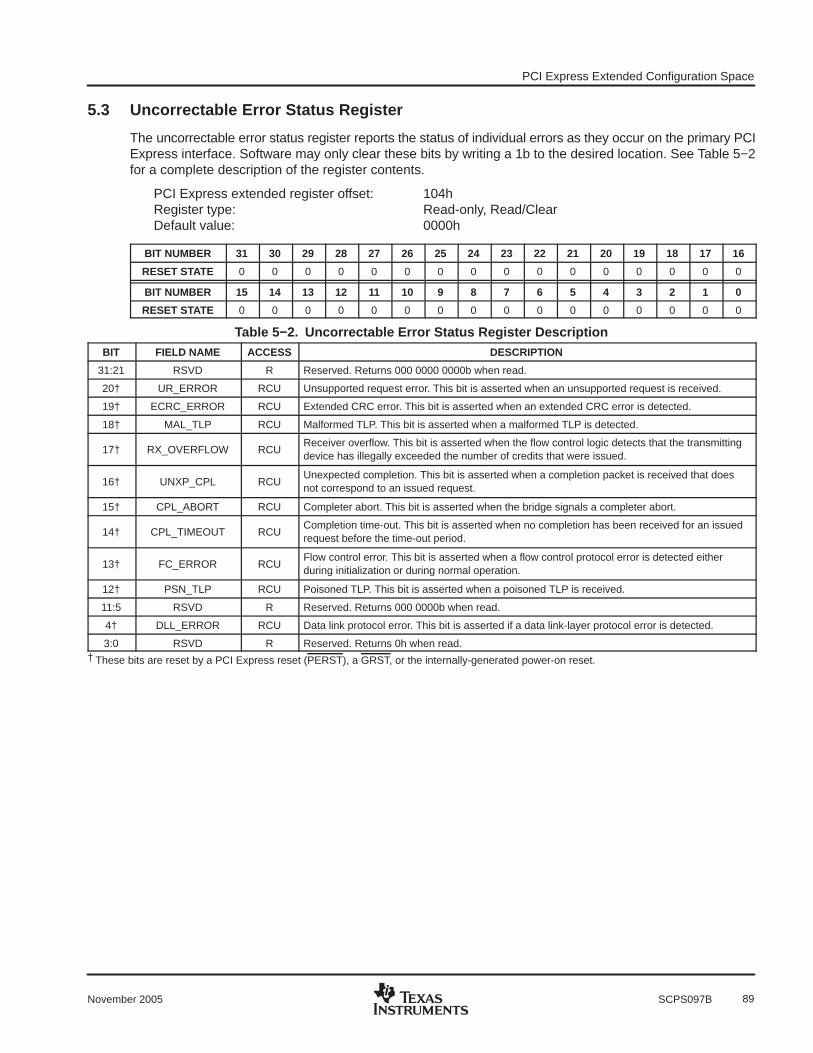
PCI Express Extended Configuration Space
89November 2005 SCPS097B
5.3 Uncorrectable Error Status Register
The uncorrectable error status register reports the status of individual errors as they occur on the primary PCIExpress interface. Software may only clear these bits by writing a 1b to the desired location. See Table 5−2for a complete description of the register contents.
PCI Express extended register offset: 104hRegister type: Read-only, Read/ClearDefault value: 0000h
BIT NUMBER 31 30 29 28 27 26 25 24 23 22 21 20 19 18 17 16
RESET STATE 0 0 0 0 0 0 0 0 0 0 0 0 0 0 0 0
BIT NUMBER 15 14 13 12 11 10 9 8 7 6 5 4 3 2 1 0
RESET STATE 0 0 0 0 0 0 0 0 0 0 0 0 0 0 0 0
Table 5−2. Uncorrectable Error Status Register DescriptionBIT FIELD NAME ACCESS DESCRIPTION
31:21 RSVD R Reserved. Returns 000 0000 0000b when read.
20† UR_ERROR RCU Unsupported request error. This bit is asserted when an unsupported request is received.
19† ECRC_ERROR RCU Extended CRC error. This bit is asserted when an extended CRC error is detected.
18† MAL_TLP RCU Malformed TLP. This bit is asserted when a malformed TLP is detected.
17† RX_OVERFLOW RCUReceiver overflow. This bit is asserted when the flow control logic detects that the transmittingdevice has illegally exceeded the number of credits that were issued.
16† UNXP_CPL RCUUnexpected completion. This bit is asserted when a completion packet is received that doesnot correspond to an issued request.
15† CPL_ABORT RCU Completer abort. This bit is asserted when the bridge signals a completer abort.
14† CPL_TIMEOUT RCUCompletion time-out. This bit is asserted when no completion has been received for an issuedrequest before the time-out period.
13† FC_ERROR RCUFlow control error. This bit is asserted when a flow control protocol error is detected eitherduring initialization or during normal operation.
12† PSN_TLP RCU Poisoned TLP. This bit is asserted when a poisoned TLP is received.
11:5 RSVD R Reserved. Returns 000 0000b when read.
4† DLL_ERROR RCU Data link protocol error. This bit is asserted if a data link-layer protocol error is detected.
3:0 RSVD R Reserved. Returns 0h when read.† These bits are reset by a PCI Express reset (PERST), a GRST, or the internally-generated power-on reset.

PCI Express Extended Configuration Space
90 November 2005SCPS097B
5.4 Uncorrectable Error Mask Register
The uncorrectable error mask register controls the reporting of individual errors as they occur. When a maskbit is set to 1b, the corresponding error status bit is not set, PCI Express error messages are blocked, theheader log is not loaded, and the first error pointer is not updated. See Table 5−3 for a complete descriptionof the register contents.
PCI Express extended register offset: 108hRegister type: Read-only, Read/WriteDefault value: 0000h
BIT NUMBER 31 30 29 28 27 26 25 24 23 22 21 20 19 18 17 16
RESET STATE 0 0 0 0 0 0 0 0 0 0 0 0 0 0 0 0
BIT NUMBER 15 14 13 12 11 10 9 8 7 6 5 4 3 2 1 0
RESET STATE 0 0 0 0 0 0 0 0 0 0 0 0 0 0 0 0
Table 5−3. Uncorrectable Error Mask Register DescriptionBIT FIELD NAME ACCESS DESCRIPTION
31:21 RSVD R Reserved. Returns 000 0000 0000b when read.
20† UR_ERROR_MASK RWUnsupported request error mask
0 = Error condition is unmasked (default)1 = Error condition is masked
19† ECRC_ERROR_MASK RWExtended CRC error mask
0 = Error condition is unmasked (default)1 = Error condition is masked
18† MAL_TLP_MASK RWMalformed TLP mask
0 = Error condition is unmasked (default)1 = Error condition is masked
17† RX_OVERFLOW_MASK RWReceiver overflow mask
0 = Error condition is unmasked (default)1 = Error condition is masked
16† UNXP_CPL_MASK RWUnexpected completion mask
0 = Error condition is unmasked (default)1 = Error condition is masked
15† CPL_ABORT_MASK RWCompleter abort mask
0 = Error condition is unmasked (default)1 = Error condition is masked
14† CPL_TIMEOUT_MASK RWCompletion time-out mask
0 = Error condition is unmasked (default)1 = Error condition is masked
13† FC_ERROR_MASK RWFlow control error mask
0 = Error condition is unmasked (default)1 = Error condition is masked
12† PSN_TLP_MASK RWPoisoned TLP mask
0 = Error condition is unmasked (default)1 = Error condition is masked
11:5 RSVD R Reserved. Returns 000 0000b when read.
4† DLL_ERROR_MASK RWData link protocol error mask
0 = Error condition is unmasked (default)1 = Error condition is masked
3:0 RSVD R Reserved. Returns 0h when read.† These bits are reset by a PCI Express reset (PERST), a GRST, or the internally-generated power-on reset.
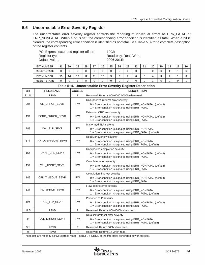
PCI Express Extended Configuration Space
91November 2005 SCPS097B
5.5 Uncorrectable Error Severity Register
The uncorrectable error severity register controls the reporting of individual errors as ERR_FATAL orERR_NONFATAL. When a bit is set, the corresponding error condition is identified as fatal. When a bit iscleared, the corresponding error condition is identified as nonfatal. See Table 5−4 for a complete descriptionof the register contents.
PCI Express extended register offset: 10ChRegister type: Read-only, Read/WriteDefault value: 0006 2011h
BIT NUMBER 31 30 29 28 27 26 25 24 23 22 21 20 19 18 17 16
RESET STATE 0 0 0 0 0 0 0 0 0 0 0 0 0 1 1 0
BIT NUMBER 15 14 13 12 11 10 9 8 7 6 5 4 3 2 1 0
RESET STATE 0 0 1 0 0 0 0 0 0 0 0 1 0 0 0 1
Table 5−4. Uncorrectable Error Severity Register DescriptionBIT FIELD NAME ACCESS DESCRIPTION
31:21 RSVD R Reserved. Returns 000 0000 0000b when read.
20† UR_ERROR_SEVR RWUnsupported request error severity
0 = Error condition is signaled using ERR_NONFATAL (default)1 = Error condition is signaled using ERR_FATAL
19† ECRC_ERROR_SEVR RWExtended CRC error severity
0 = Error condition is signaled using ERR_NONFATAL (default)1 = Error condition is signaled using ERR_FATAL
18† MAL_TLP_SEVR RWMalformed TLP severity
0 = Error condition is signaled using ERR_NONFATAL1 = Error condition is signaled using ERR_FATAL (default)
17† RX_OVERFLOW_SEVR RWReceiver overflow severity
0 = Error condition is signaled using ERR_NONFATAL1 = Error condition is signaled using ERR_FATAL (default)
16† UNXP_CPL_SEVR RWUnexpected completion severity
0 = Error condition is signaled using ERR_NONFATAL (default)1 = Error condition is signaled using ERR_FATAL
15† CPL_ABORT_SEVR RWCompleter abort severity
0 = Error condition is signaled using ERR_NONFATAL (default)1 = Error condition is signaled using ERR_FATAL
14† CPL_TIMEOUT_SEVR RWCompletion time-out severity
0 = Error condition is signaled using ERR_NONFATAL (default)1 = Error condition is signaled using ERR_FATAL
13† FC_ERROR_SEVR RWFlow control error severity
0 = Error condition is signaled using ERR_NONFATAL1 = Error condition is signaled using ERR_FATAL (default)
12† PSN_TLP_SEVR RWPoisoned TLP severity
0 = Error condition is signaled using ERR_NONFATAL (default)1 = Error condition is signaled using ERR_FATAL
11:5 RSVD R Reserved. Returns 000 0000b when read.
4† DLL_ERROR_SEVR RWData link protocol error severity
0 = Error condition is signaled using ERR_NONFATAL1 = Error condition is signaled using ERR_FATAL (default)
3:1 RSVD R Reserved. Return 000b when read.
0 RSVD R Reserved. Returns 1b when read.† These bits are reset by a PCI Express reset (PERST), a GRST, or the internally-generated power-on reset.

PCI Express Extended Configuration Space
92 November 2005SCPS097B
5.6 Correctable Error Status Register
The correctable error status register reports the status of individual errors as they occur. Software may onlyclear these bits by writing a 1b to the desired location. See Table 5−5 for a complete description of the registercontents.
PCI Express extended register offset: 110hRegister type: Read-only, Read/ClearDefault value: 0000 0000h
BIT NUMBER 31 30 29 28 27 26 25 24 23 22 21 20 19 18 17 16
RESET STATE 0 0 0 0 0 0 0 0 0 0 0 0 0 0 0 0
BIT NUMBER 15 14 13 12 11 10 9 8 7 6 5 4 3 2 1 0
RESET STATE 0 0 0 0 0 0 0 0 0 0 0 0 0 0 0 0
Table 5−5. Correctable Error Status Register DescriptionBIT FIELD NAME ACCESS DESCRIPTION
31:13 RSVD R Reserved. Returns 000 0000 0000 0000 0000b when read.
12† REPLAY_TMOUT RCUReplay timer time-out. This bit is asserted when the replay timer expires for a pending requestor completion that has not been acknowledged.
11:9 RSVD R Reserved. Returns 000b when read.
8† REPLAY_ROLL RCUREPLAY_NUM rollover. This bit is asserted when the replay counter rolls over after a pendingrequest or completion has not been acknowledged.
7† BAD_DLLP RCUBad DLLP error. This bit is asserted when an 8b/10b error was detected by the PHY during thereception of a DLLP.
6† BAD_TLP RCUBad TLP error. This bit is asserted when an 8b/10b error was detected by the PHY during thereception of a TLP.
5:1 RSVD R Reserved. Returns 00000b when read.
0† RX_ERROR RCU Receiver error. This bit is asserted when an 8b/10b error is detected by the PHY at any time.† These bits are reset by a PCI Express reset (PERST), a GRST, or the internally-generated power-on reset.

PCI Express Extended Configuration Space
93November 2005 SCPS097B
5.7 Correctable Error Mask Register
The correctable error mask register controls the reporting of individual errors as they occur. When a mask bitis set to 1b, the corresponding error status bit is not set, PCI Express error messages are blocked, the headerlog is not loaded, and the first error pointer is not updated. See Table 5−6 for a complete description of theregister contents.
PCI Express extended register offset: 114hRegister type: Read-only, Read/WriteDefault value: 0000 0000h
BIT NUMBER 31 30 29 28 27 26 25 24 23 22 21 20 19 18 17 16
RESET STATE 0 0 0 0 0 0 0 0 0 0 0 0 0 0 0 0
BIT NUMBER 15 14 13 12 11 10 9 8 7 6 5 4 3 2 1 0
RESET STATE 0 0 0 0 0 0 0 0 0 0 0 0 0 0 0 0
Table 5−6. Correctable Error Mask Register DescriptionBIT FIELD NAME ACCESS DESCRIPTION
31:13 RSVD R Reserved. Returns 000 0000 0000 0000 0000b when read.
12† REPLAY_TMOUT_MASK RWReplay timer time-out mask.
0 = Error condition is unmasked (default)1 = Error condition is masked
11:9 RSVD R Reserved. Returns 000b when read.
8† REPLAY_ROLL_MASK RWREPLAY_NUM rollover mask.
0 = Error condition is unmasked (default)1 = Error condition is masked
7† BAD_DLLP_MASK RWBad DLLP error mask.
0 = Error condition is unmasked (default)1 = Error condition is masked
6† BAD_TLP_MASK RWBad TLP error mask.
0 = Error condition is unmasked (default)1 = Error condition is masked
5:1 RSVD R Reserved. Returns 00000b when read.
0† RX_ERROR_MASK RWReceiver error mask.
0 = Error condition is unmasked (default)1 = Error condition is masked
† These bits are reset by a PCI Express reset (PERST), a GRST, or the internally-generated power-on reset.

PCI Express Extended Configuration Space
94 November 2005SCPS097B
5.8 Advanced Error Capabilities and Control Register
The advanced error capabilities and control register allows the system to monitor and control the advancederror reporting capabilities. See Table 5−7 for a complete description of the register contents.
PCI Express extended register offset: 118hRegister type: Read-only, Read/WriteDefault value: 0000 00A0h
BIT NUMBER 31 30 29 28 27 26 25 24 23 22 21 20 19 18 17 16
RESET STATE 0 0 0 0 0 0 0 0 0 0 0 0 0 0 0 0
BIT NUMBER 15 14 13 12 11 10 9 8 7 6 5 4 3 2 1 0
RESET STATE 0 0 0 0 0 0 0 0 1 0 1 0 0 0 0 0
Table 5−7. Advanced Error Capabilities and Control Register DescriptionBIT FIELD NAME ACCESS DESCRIPTION
31:9 RSVD R Reserved. Returns 000 0000 0000 0000 0000 0000b when read.
8† ECRC_CHK_EN RWExtended CRC check enable
0 = Extended CRC checking is disabled1 = Extended CRC checking is enabled
7 ECRC_CHK_CAPABLE RExtended CRC check capable. This read-only bit returns a value of 1b indicating that thebridge is capable of checking extended CRC information.
6† ECRC_GEN_EN RWExtended CRC generation enable
0 = Extended CRC generation is disabled1 = Extended CRC generation is enabled
5 ECRC_GEN_CAPABLE RExtended CRC generation capable. This read-only bit returns a value of 1b indicating thatthe bridge is capable of generating extended CRC information.
4:0† FIRST_ERR RUFirst error pointer. This 5-bit value reflects the bit position within the uncorrectable errorstatus register (offset 104h, see Section 5.3) corresponding to the class of the first errorcondition that was detected.
† These bits are reset by a PCI Express reset (PERST), a GRST, or the internally-generated power-on reset.
5.9 Header Log Register
The header log register stores the TLP header for the packet that lead to the most recently detected errorcondition. Offset 11Ch contains the first DWORD. Offset 128h contains the last DWORD (in the case of a 4DWTLP header). Each DWORD is stored with the least significant byte representing the earliest transmitted.These bits are reset by a PCI Express reset (PERST), a GRST, or the internally-generated power-on reset.
PCI Express extended register offset: 11Ch, 120h, 124h, and 128hRegister type: Read-onlyDefault value: 0000 0000h
BIT NUMBER 31 30 29 28 27 26 25 24 23 22 21 20 19 18 17 16
RESET STATE 0 0 0 0 0 0 0 0 0 0 0 0 0 0 0 0
BIT NUMBER 15 14 13 12 11 10 9 8 7 6 5 4 3 2 1 0
RESET STATE 0 0 0 0 0 0 0 0 0 0 0 0 0 0 0 0

PCI Express Extended Configuration Space
95November 2005 SCPS097B
5.10 Secondary Uncorrectable Error Status Register
The secondary uncorrectable error status register reports the status of individual PCI bus errors as they occur.Software may only clear these bits by writing a 1b to the desired location. See Table 5−8 for a completedescription of the register contents.
PCI Express extended register offset: 12ChRegister type: Read-only, Read/ClearDefault value: 0000 0000h
BIT NUMBER 31 30 29 28 27 26 25 24 23 22 21 20 19 18 17 16
RESET STATE 0 0 0 0 0 0 0 0 0 0 0 0 0 0 0 0
BIT NUMBER 15 14 13 12 11 10 9 8 7 6 5 4 3 2 1 0
RESET STATE 0 0 0 0 0 0 0 0 0 0 0 0 0 0 0 0
Table 5−8. Secondary Uncorrectable Error Status Register DescriptionBIT FIELD NAME ACCESS DESCRIPTION
31:14 RSVD R Reserved. Returns 00 0000 0000 0000 0000b when read.
13† BRIDGE_ERROR R Internal bridge error. This error bit is associated with a PCI-X error and returns 0b when read.
12† SERR_DETECT RCUSERR assertion detected. This bit is asserted when the bridge detects the assertion of SERRon the secondary bus.
11† PERR_DETECT RCUPERR assertion detected. This bit is asserted when the bridge detects the assertion of PERRon the secondary bus.
10† DISCARD_TIMER RCUDelayed transaction discard timer expired. This bit is asserted when the discard timer expiresfor a pending delayed transaction that was initiated on the secondary bus.
9† UNCOR_ADDR RCUUncorrectable address error. This bit is asserted when the bridge detects a parity error duringthe address phase of an upstream transaction.
8† ATTR_ERROR RUncorrectable attribute error. This error bit is associated with a PCI-X error and returns 0bwhen read.
7† UNCOR_DATA RCUUncorrectable data error. This bit is asserted when the bridge detects a parity error during adata phase of an upstream write transaction, or when the bridge detects the assertion ofPERR when forwarding read completion data to a PCI device.
6† SC_MSG_DATA RUncorrectable split completion message data error. This error bit is associated with a PCI-Xerror and returns 0b when read.
5† SC_ERROR RUnexpected split completion error. This error bit is associated with a PCI-X error and returns0b when read.
4 RSVD R Reserved. Returns 0b when read.
3† MASTER_ABORT RCUReceived master abort. This bit is asserted when the bridge receives a master abort on thePCI interface.
2† TARGET_ABORT RCUReceived target abort. This bit is asserted when the bridge receives a target abort on the PCIinterface.
1† SC_MSTR_ABORT RMaster abort on split completion. This error bit is associated with a PCI-X error and returns 0bwhen read.
0 RSVD R Reserved. Returns 0b when read.† These bits are reset by a PCI Express reset (PERST), a GRST, or the internally-generated power-on reset.

PCI Express Extended Configuration Space
96 November 2005SCPS097B
5.11 Secondary Uncorrectable Error Mask Register
The secondary uncorrectable error mask register controls the reporting of individual errors as they occur.When a mask bit is set to 1b, the corresponding error status bit is not set, PCI Express error messages areblocked, the header log is not loaded, and the first error pointer is not updated. See Table 5−9 for a completedescription of the register contents.
PCI Express extended register offset: 130hRegister type: Read-only, Read/WriteDefault value: 0000 17A8h
BIT NUMBER 31 30 29 28 27 26 25 24 23 22 21 20 19 18 17 16
RESET STATE 0 0 0 0 0 0 0 0 0 0 0 0 0 0 0 0
BIT NUMBER 15 14 13 12 11 10 9 8 7 6 5 4 3 2 1 0
RESET STATE 0 0 0 1 0 1 1 1 1 0 1 0 1 0 0 0
Table 5−9. Secondary Uncorrectable Error Mask Register DescriptionBIT FIELD NAME ACCESS DESCRIPTION
31:14 RSVD R Reserved. Returns 00 0000 0000 0000 0000b when read.
13† BRIDGE_ERROR_MASK RWInternal bridge error. This mask bit is associated with a PCI-X error and has no effecton the bridge.
12† SERR_DETECT_MASK RWSERR assertion detected
0 = Error condition is unmasked1 = Error condition is masked (default)
11† PERR_DETECT_MASK RWPERR assertion detected
0 = Error condition is unmasked (default)1 = Error condition is masked
10† DISCARD_TIMER_MASK RWDelayed transaction discard timer expired
0 = Error condition is unmasked1 = Error condition is masked (default)
9† UNCOR_ADDR_MASK RWUncorrectable address error
0 = Error condition is unmasked1 = Error condition is masked (default)
8† ATTR_ERROR_MASK RWUncorrectable attribute error. This mask bit is associated with a PCI-X error and has noeffect on the bridge.
7† UNCOR_DATA_MASK RWUncorrectable data error
0 = Error condition is unmasked1 = Error condition is masked (default)
6† SC_MSG_DATA_MASK RWUncorrectable split completion message data error. This mask bit is associated with aPCI-X error and has no effect on the bridge.
5† SC_ERROR_MASK RWUnexpected split completion error. This mask bit is associated with a PCI-X error andhas no effect on the bridge.
4 RSVD R Reserved. Returns 0b when read.
3† MASTER_ABORT_MASK RWReceived master abort
0 = Error condition is unmasked1 = Error condition is masked (default)
2† TARGET_ABORT_MASK RWReceived target abort
0 = Error condition is unmasked (default)1 = Error condition is masked
1† SC_MSTR_ABORT_MASK RWMaster abort on split completion. This mask bit is associated with a PCI-X error andhas no effect on the bridge.
0 RSVD R Reserved. Returns 0b when read.† These bits are reset by a PCI Express reset (PERST), a GRST, or the internally-generated power-on reset.
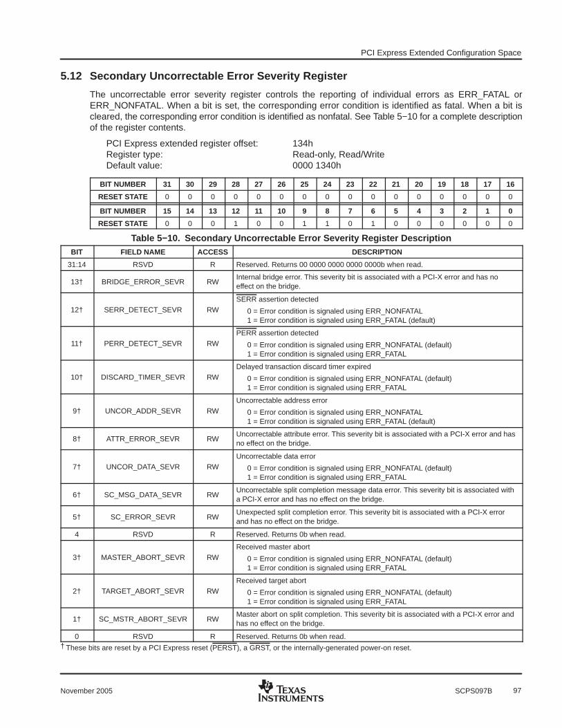
PCI Express Extended Configuration Space
97November 2005 SCPS097B
5.12 Secondary Uncorrectable Error Severity Register
The uncorrectable error severity register controls the reporting of individual errors as ERR_FATAL orERR_NONFATAL. When a bit is set, the corresponding error condition is identified as fatal. When a bit iscleared, the corresponding error condition is identified as nonfatal. See Table 5−10 for a complete descriptionof the register contents.
PCI Express extended register offset: 134hRegister type: Read-only, Read/WriteDefault value: 0000 1340h
BIT NUMBER 31 30 29 28 27 26 25 24 23 22 21 20 19 18 17 16
RESET STATE 0 0 0 0 0 0 0 0 0 0 0 0 0 0 0 0
BIT NUMBER 15 14 13 12 11 10 9 8 7 6 5 4 3 2 1 0
RESET STATE 0 0 0 1 0 0 1 1 0 1 0 0 0 0 0 0
Table 5−10. Secondary Uncorrectable Error Severity Register DescriptionBIT FIELD NAME ACCESS DESCRIPTION
31:14 RSVD R Reserved. Returns 00 0000 0000 0000 0000b when read.
13† BRIDGE_ERROR_SEVR RWInternal bridge error. This severity bit is associated with a PCI-X error and has noeffect on the bridge.
12† SERR_DETECT_SEVR RWSERR assertion detected
0 = Error condition is signaled using ERR_NONFATAL1 = Error condition is signaled using ERR_FATAL (default)
11† PERR_DETECT_SEVR RWPERR assertion detected
0 = Error condition is signaled using ERR_NONFATAL (default)1 = Error condition is signaled using ERR_FATAL
10† DISCARD_TIMER_SEVR RWDelayed transaction discard timer expired
0 = Error condition is signaled using ERR_NONFATAL (default)1 = Error condition is signaled using ERR_FATAL
9† UNCOR_ADDR_SEVR RWUncorrectable address error
0 = Error condition is signaled using ERR_NONFATAL1 = Error condition is signaled using ERR_FATAL (default)
8† ATTR_ERROR_SEVR RWUncorrectable attribute error. This severity bit is associated with a PCI-X error and hasno effect on the bridge.
7† UNCOR_DATA_SEVR RWUncorrectable data error
0 = Error condition is signaled using ERR_NONFATAL (default)1 = Error condition is signaled using ERR_FATAL
6† SC_MSG_DATA_SEVR RWUncorrectable split completion message data error. This severity bit is associated witha PCI-X error and has no effect on the bridge.
5† SC_ERROR_SEVR RWUnexpected split completion error. This severity bit is associated with a PCI-X errorand has no effect on the bridge.
4 RSVD R Reserved. Returns 0b when read.
3† MASTER_ABORT_SEVR RWReceived master abort
0 = Error condition is signaled using ERR_NONFATAL (default)1 = Error condition is signaled using ERR_FATAL
2† TARGET_ABORT_SEVR RWReceived target abort
0 = Error condition is signaled using ERR_NONFATAL (default)1 = Error condition is signaled using ERR_FATAL
1† SC_MSTR_ABORT_SEVR RWMaster abort on split completion. This severity bit is associated with a PCI-X error andhas no effect on the bridge.
0 RSVD R Reserved. Returns 0b when read.† These bits are reset by a PCI Express reset (PERST), a GRST, or the internally-generated power-on reset.

PCI Express Extended Configuration Space
98 November 2005SCPS097B
5.13 Secondary Error Capabilities and Control Register
The secondary error capabilities and control register allows the system to monitor and control the secondaryadvanced error reporting capabilities. See Table 5−11 for a complete description of the register contents.
PCI Express extended register offset: 138hRegister type: Read-onlyDefault value: 0000 0000h
BIT NUMBER 31 30 29 28 27 26 25 24 23 22 21 20 19 18 17 16
RESET STATE 0 0 0 0 0 0 0 0 0 0 0 0 0 0 0 0
BIT NUMBER 15 14 13 12 11 10 9 8 7 6 5 4 3 2 1 0
RESET STATE 0 0 0 0 0 0 0 0 0 0 0 0 0 0 0 0
Table 5−11. Secondary Error Capabilities and Control Register DescriptionBIT FIELD NAME ACCESS DESCRIPTION
31:5 RSVD R Reserved. Returns 000 0000 0000 0000 0000 0000 0000b when read.
4:0† SEC_FIRST_ERR RUFirst error pointer. This 5-bit value reflects the bit position within the secondary uncorrectableerror status register (offset 12Ch, see Section 5.10) corresponding to the class of the first errorcondition that was detected.
† These bits are reset by a PCI Express reset (PERST), a GRST, or the internally-generated power-on reset.
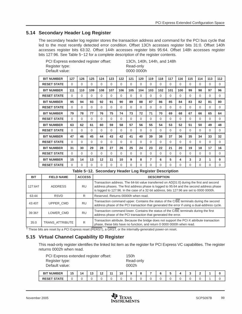
PCI Express Extended Configuration Space
99November 2005 SCPS097B
5.14 Secondary Header Log Register
The secondary header log register stores the transaction address and command for the PCI bus cycle thatled to the most recently detected error condition. Offset 13Ch accesses register bits 31:0. Offset 140haccesses register bits 63:32. Offset 144h accesses register bits 95:64. Offset 148h accesses registerbits 127:96. See Table 5−12 for a complete description of the register contents.
PCI Express extended register offset: 13Ch, 140h, 144h, and 148hRegister type: Read-onlyDefault value: 0000 0000h
BIT NUMBER 127 126 125 124 123 122 121 120 119 118 117 116 115 114 113 112
RESET STATE 0 0 0 0 0 0 0 0 0 0 0 0 0 0 0 0
BIT NUMBER 111 110 109 108 107 106 105 104 103 102 101 100 99 98 97 96
RESET STATE 0 0 0 0 0 0 0 0 0 0 0 0 0 0 0 0
BIT NUMBER 95 94 93 92 91 90 89 88 87 86 85 84 83 82 81 80
RESET STATE 0 0 0 0 0 0 0 0 0 0 0 0 0 0 0 0
BIT NUMBER 79 78 77 76 75 74 73 72 71 70 69 68 67 66 65 64
RESET STATE 0 0 0 0 0 0 0 0 0 0 0 0 0 0 0 0
BIT NUMBER 63 62 61 60 59 58 57 56 55 54 53 52 51 50 49 48
RESET STATE 0 0 0 0 0 0 0 0 0 0 0 0 0 0 0 0
BIT NUMBER 47 46 45 44 43 42 41 40 39 38 37 36 35 34 33 32
RESET STATE 0 0 0 0 0 0 0 0 0 0 0 0 0 0 0 0
BIT NUMBER 31 30 29 28 27 26 25 24 23 22 21 20 19 18 17 16
RESET STATE 0 0 0 0 0 0 0 0 0 0 0 0 0 0 0 0
BIT NUMBER 15 14 13 12 11 10 9 8 7 6 5 4 3 2 1 0
RESET STATE 0 0 0 0 0 0 0 0 0 0 0 0 0 0 0 0
Table 5−12. Secondary Header Log Register DescriptionBIT FIELD NAME ACCESS DESCRIPTION
127:64† ADDRESS RUTransaction address. The 64-bit value transferred on AD[31:0] during the first and secondaddress phases. The first address phase is logged to 95:64 and the second address phaseis logged to 127:96. In the case of a 32-bit address, bits 127:96 are set to 0000 0000h.
63:44 RSVD R Reserved. Returns 00000h when read.
43:40† UPPER_CMD RUTransaction command upper. Contains the status of the C/BE terminals during the secondaddress phase of the PCI transaction that generated the error if using a dual-address cycle.
39:36† LOWER_CMD RUTransaction command lower. Contains the status of the C/BE terminals during the firstaddress phase of the PCI transaction that generated the error.
35:0 TRANS_ATTRIBUTE RTransaction attribute. Because the bridge does not support the PCI-X attribute transactionphase, these bits have no function, and return 0 0000 0000h when read.
† These bits are reset by a PCI Express reset (PERST), a GRST, or the internally-generated power-on reset.
5.15 Virtual Channel Capability ID Register
This read-only register identifies the linked list item as the register for PCI Express VC capabilities. The registerreturns 0002h when read.
PCI Express extended register offset: 150hRegister type: Read-onlyDefault value: 0002h
BIT NUMBER 15 14 13 12 11 10 9 8 7 6 5 4 3 2 1 0
RESET STATE 0 0 0 0 0 0 0 0 0 0 0 0 0 0 1 0

PCI Express Extended Configuration Space
100 November 2005SCPS097B
5.16 Next Capability Offset/Capability Version Register
This read-only register returns the value 000h to indicate that this extended capability block represents theend of the linked list of extended capability structures. The four least significant bits identify the revision of thecurrent capability block as 1h.
PCI Express extended register offset: 152hRegister type: Read-onlyDefault value: 0001h
BIT NUMBER 15 14 13 12 11 10 9 8 7 6 5 4 3 2 1 0
RESET STATE 0 0 0 0 0 0 0 0 0 0 0 0 0 0 0 1
5.17 Port VC Capability Register 1
The first port VC capability register provides information to software regarding the VC capabilities support bythe bridge. See Table 5−13 for a complete description of the register contents.
PCI Express extended register offset: 154hRegister type: Read-onlyDefault value: 0000 08X1h
BIT NUMBER 31 30 29 28 27 26 25 24 23 22 21 20 19 18 17 16
RESET STATE 0 0 0 0 0 0 0 0 0 0 0 0 0 0 0 0
BIT NUMBER 15 14 13 12 11 10 9 8 7 6 5 4 3 2 1 0
RESET STATE 0 0 0 0 1 0 0 0 0 0 0 x 0 0 0 1
Table 5−13. Port VC Capability Register 1 DescriptionBIT FIELD NAME ACCESS DESCRIPTION
31:12 RSVD R Reserved. Returns 00000h when read.
11:10 PORT_TABLE_SIZE RPort arbitration table entry size. This read-only field returns a value of 10b to indicatethat the field size within the port arbitration table is four bits. This is necessary to allowas many as six secondary PCI bus masters.
9:8 REF_CLK RReference clock. This read-only field returns a value of 00b to indicate than an internal100-ns timer is used for time-based, WRR port arbitration.
7 RSVD R Reserved. Returns 0b when read.
6:4 LOW_PRIORITY_COUNT RU
Low priority extended VC count. When bit 25 (STRICT_PRIORITY_EN) in the generalcontrol register (offset D4h, see Section 4.65) is 0b, the defaultLOW_PRIORITY_COUNT is 001b. When STRICT_PRIORITY_EN is 1b, the defaultLOW_PRIORITY_COUNT is 000b. When STRICT_PRIORITY_EN is set, strict priorityVC arbitration is used and the extended VC always receives priority over VC0 at thePCI Express port.
3 RSVD R Reserved. Returns 0b when read.
2:0 EXT_VC_COUNT RExtended VC count. This read-only field returns a value of 001b to indicate support forone extended VC.
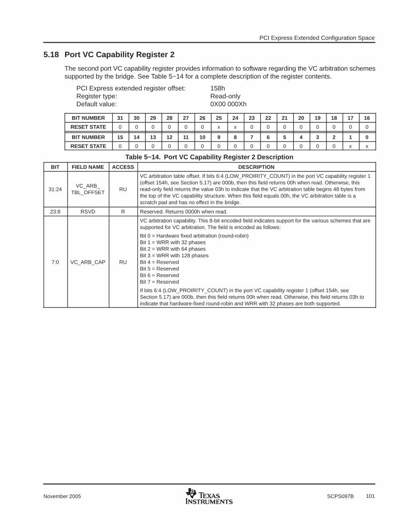
PCI Express Extended Configuration Space
101November 2005 SCPS097B
5.18 Port VC Capability Register 2
The second port VC capability register provides information to software regarding the VC arbitration schemessupported by the bridge. See Table 5−14 for a complete description of the register contents.
PCI Express extended register offset: 158hRegister type: Read-onlyDefault value: 0X00 000Xh
BIT NUMBER 31 30 29 28 27 26 25 24 23 22 21 20 19 18 17 16
RESET STATE 0 0 0 0 0 0 x x 0 0 0 0 0 0 0 0
BIT NUMBER 15 14 13 12 11 10 9 8 7 6 5 4 3 2 1 0
RESET STATE 0 0 0 0 0 0 0 0 0 0 0 0 0 0 x x
Table 5−14. Port VC Capability Register 2 DescriptionBIT FIELD NAME ACCESS DESCRIPTION
31:24VC_ARB_
TBL_OFFSETRU
VC arbitration table offset. If bits 6:4 (LOW_PROIRITY_COUNT) in the port VC capability register 1(offset 154h, see Section 5.17) are 000b, then this field returns 00h when read. Otherwise, thisread-only field returns the value 03h to indicate that the VC arbitration table begins 48 bytes fromthe top of the VC capability structure. When this field equals 00h, the VC arbitration table is ascratch pad and has no effect in the bridge.
23:8 RSVD R Reserved. Returns 0000h when read.
7:0 VC_ARB_CAP RU
VC arbitration capability. This 8-bit encoded field indicates support for the various schemes that aresupported for VC arbitration. The field is encoded as follows:
Bit 0 = Hardware fixed arbitration (round-robin)Bit 1 = WRR with 32 phasesBit 2 = WRR with 64 phasesBit 3 = WRR with 128 phasesBit 4 = ReservedBit 5 = ReservedBit 6 = ReservedBit 7 = Reserved
If bits 6:4 (LOW_PROIRITY_COUNT) in the port VC capability register 1 (offset 154h, seeSection 5.17) are 000b, then this field returns 00h when read. Otherwise, this field returns 03h toindicate that hardware-fixed round-robin and WRR with 32 phases are both supported.
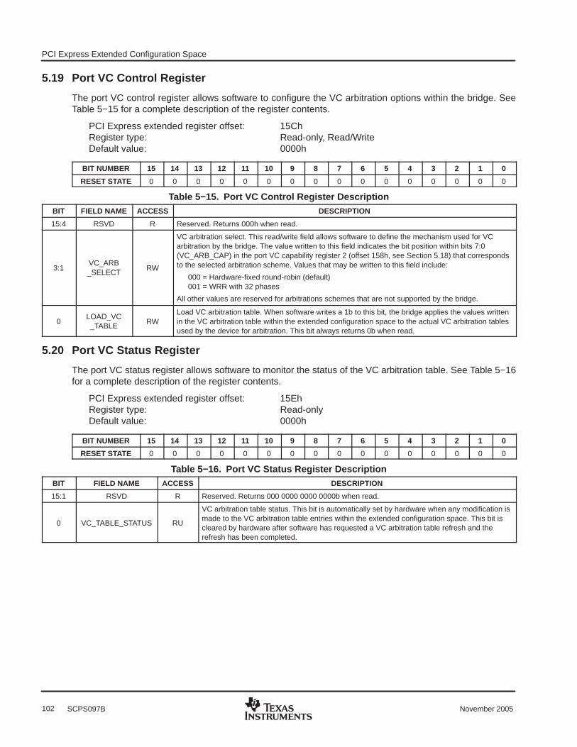
PCI Express Extended Configuration Space
102 November 2005SCPS097B
5.19 Port VC Control Register
The port VC control register allows software to configure the VC arbitration options within the bridge. SeeTable 5−15 for a complete description of the register contents.
PCI Express extended register offset: 15ChRegister type: Read-only, Read/WriteDefault value: 0000h
BIT NUMBER 15 14 13 12 11 10 9 8 7 6 5 4 3 2 1 0
RESET STATE 0 0 0 0 0 0 0 0 0 0 0 0 0 0 0 0
Table 5−15. Port VC Control Register DescriptionBIT FIELD NAME ACCESS DESCRIPTION
15:4 RSVD R Reserved. Returns 000h when read.
3:1VC_ARB_SELECT
RW
VC arbitration select. This read/write field allows software to define the mechanism used for VCarbitration by the bridge. The value written to this field indicates the bit position within bits 7:0(VC_ARB_CAP) in the port VC capability register 2 (offset 158h, see Section 5.18) that correspondsto the selected arbitration scheme. Values that may be written to this field include:
000 = Hardware-fixed round-robin (default)001 = WRR with 32 phases
All other values are reserved for arbitrations schemes that are not supported by the bridge.
0LOAD_VC_TABLE
RWLoad VC arbitration table. When software writes a 1b to this bit, the bridge applies the values writtenin the VC arbitration table within the extended configuration space to the actual VC arbitration tablesused by the device for arbitration. This bit always returns 0b when read.
5.20 Port VC Status Register
The port VC status register allows software to monitor the status of the VC arbitration table. See Table 5−16for a complete description of the register contents.
PCI Express extended register offset: 15EhRegister type: Read-onlyDefault value: 0000h
BIT NUMBER 15 14 13 12 11 10 9 8 7 6 5 4 3 2 1 0
RESET STATE 0 0 0 0 0 0 0 0 0 0 0 0 0 0 0 0
Table 5−16. Port VC Status Register DescriptionBIT FIELD NAME ACCESS DESCRIPTION
15:1 RSVD R Reserved. Returns 000 0000 0000 0000b when read.
0 VC_TABLE_STATUS RU
VC arbitration table status. This bit is automatically set by hardware when any modification ismade to the VC arbitration table entries within the extended configuration space. This bit iscleared by hardware after software has requested a VC arbitration table refresh and therefresh has been completed.

PCI Express Extended Configuration Space
103November 2005 SCPS097B
5.21 VC Resource Capability Register (VC0)
The VC resource capability register for VC0 provides information to software regarding the port and arbitrationschemes supported by the bridge. See Table 5−17 for a complete description of the register contents.
PCI Express extended register offset: 160hRegister type: Read-onlyDefault value: 0000 0001h
BIT NUMBER 31 30 29 28 27 26 25 24 23 22 21 20 19 18 17 16
RESET STATE 0 0 0 0 0 0 0 0 0 0 0 0 0 0 0 0
BIT NUMBER 15 14 13 12 11 10 9 8 7 6 5 4 3 2 1 0
RESET STATE 0 0 0 0 0 0 0 0 0 0 0 0 0 0 0 1
Table 5−17. VC Resource Capability Register (VC0) DescriptionBIT FIELD NAME ACCESS DESCRIPTION
31:24 PORT_ARB_TBL_OFFSET RPort arbitration table offset. This read-only field returns the value 00h to indicate thatno port arbitration table is required for this VC.
23 RSVD R Reserved. Returns 0b when read.
22:16 MAX_TIME_SLOTS RMaximum time slots. This read-only field returns the value 000 0000b because there isno support for time-based, WRR arbitration on this VC.
15 REJECT_SNOOP RReject snoop transactions. This bit only has meaningful context for root ports;therefore, returns 0b when read.
14 ADV_SWITCHING RAdvanced packet switching. This read-only bit returns 0b to indicate that the use of thisVC is not limited to AS traffic.
13:8 RSVD R Reserved. Returns 00 0000b when read.
7:0 PORT_ARB_CAP R
Port arbitration capability. This 8-bit encoded field indicates support for the variousschemes that are supported for port (secondary PCI device) arbitration. The field isencoded as follows:
Bit 0 = Hardware fixed arbitration (round-robin)Bit 1 = WRR with 32 phasesBit 2 = WRR with 64 phasesBit 3 = WRR with 128 phasesBit 4 = Time-based WRR with 128 phasesBit 5 = WRR with 256 phasesBits 6 and 7 = Reserved
The returned value of 01h indicates that only hardware-fixed, round-robin arbitration issupport for this VC.
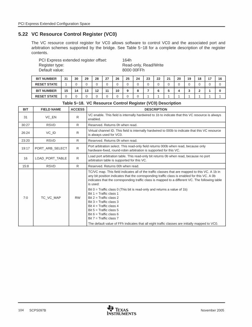
PCI Express Extended Configuration Space
104 November 2005SCPS097B
5.22 VC Resource Control Register (VC0)
The VC resource control register for VC0 allows software to control VC0 and the associated port andarbitration schemes supported by the bridge. See Table 5−18 for a complete description of the registercontents.
PCI Express extended register offset: 164hRegister type: Read-only, Read/WriteDefault value: 8000 00FFh
BIT NUMBER 31 30 29 28 27 26 25 24 23 22 21 20 19 18 17 16
RESET STATE 1 0 0 0 0 0 0 0 0 0 0 0 0 0 0 0
BIT NUMBER 15 14 13 12 11 10 9 8 7 6 5 4 3 2 1 0
RESET STATE 0 0 0 0 0 0 0 0 1 1 1 1 1 1 1 1
Table 5−18. VC Resource Control Register (VC0) DescriptionBIT FIELD NAME ACCESS DESCRIPTION
31 VC_EN RVC enable. This field is internally hardwired to 1b to indicate that this VC resource is alwaysenabled.
30:27 RSVD R Reserved. Returns 0h when read.
26:24 VC_ID RVirtual channel ID. This field is internally hardwired to 000b to indicate that this VC resourceis always used for VC0.
23:20 RSVD R Reserved. Returns 0h when read.
19:17 PORT_ARB_SELECT RPort arbitration select. This read-only field returns 000b when read, because onlyhardware-fixed, round-robin arbitration is supported for this VC.
16 LOAD_PORT_TABLE RLoad port arbitration table. This read-only bit returns 0b when read, because no portarbitration table is supported for this VC.
15:8 RSVD R Reserved. Returns 00h when read.
7:0 TC_VC_MAP RW
TC/VC map. This field indicates all of the traffic classes that are mapped to this VC. A 1b inany bit position indicates that the corresponding traffic class is enabled for this VC. A 0bindicates that the corresponding traffic class is mapped to a different VC. The following tableis used:
Bit 0 = Traffic class 0 (This bit is read-only and returns a value of 1b)Bit 1 = Traffic class 1Bit 2 = Traffic class 2Bit 3 = Traffic class 3Bit 4 = Traffic class 4Bit 5 = Traffic class 5Bit 6 = Traffic class 6Bit 7 = Traffic class 7
The default value of FFh indicates that all eight traffic classes are initially mapped to VC0.

PCI Express Extended Configuration Space
105November 2005 SCPS097B
5.23 VC Resource Status Register (VC0)The VC resource status register allows software to monitor the status of the port arbitration table for this VC.See Table 5−19 for a complete description of the register contents.
PCI Express extended register offset: 16AhRegister type: Read-onlyDefault value: 0000h
BIT NUMBER 15 14 13 12 11 10 9 8 7 6 5 4 3 2 1 0
RESET STATE 0 0 0 0 0 0 0 0 0 0 0 0 0 0 0 0
Table 5−19. VC Resource Status Register (VC0) DescriptionBIT FIELD NAME ACCESS DESCRIPTION15:2 RSVD R Reserved. Returns 00 0000 0000 0000b when read.
1 VC_PENDING RUVC negotiation pending. This bit is asserted when VC negotiation is in progress followinga request by software to enable or disable the VC or at startup for VC0.
0 PORT_TABLE_STATUS RU
Port arbitration table status. This bit is automatically set by hardware when anymodification is made to the port arbitration table entries for this VC within the extendedconfiguration space. This bit is cleared by hardware after software has requested a portarbitration table refresh and the refresh has been completed.
5.24 VC Resource Capability Register (VC1)The VC resource capability register for VC1 provides information to software regarding the port and arbitrationschemes supported by the bridge. See Table 5−20 for a complete description of the register contents.
PCI Express extended register offset: 16ChRegister type: Read-onlyDefault value: 077F 0011h
BIT NUMBER 31 30 29 28 27 26 25 24 23 22 21 20 19 18 17 16
RESET STATE 0 0 0 0 0 1 1 1 0 1 1 1 1 1 1 1
BIT NUMBER 15 14 13 12 11 10 9 8 7 6 5 4 3 2 1 0
RESET STATE 0 0 0 0 0 0 0 0 0 0 0 1 0 0 0 1
Table 5−20. VC Resource Capability Register (VC1) DescriptionBIT FIELD NAME ACCESS DESCRIPTION
31:24PORT_ARB_TBL_OFFSET
RPort arbitration table offset. This read-only field returns the value 07h to indicate that the portarbitration table for this VC begins 112 bytes from the top of the VC capability structure.
23 RSVD R Reserved. Returns 0b when read.
22:16MAX_TIME_
SLOTSR
Maximum time slots. The read-only field returns the value 111 1111b to indicate that all 128 slotsare supported for time-based WRR.
15REJECT_SNOOP
RReject snoop transactions. This bit only has meaningful context for root ports; therefore, returns 0bwhen read.
14ADV_
SWITCHINGR
Advanced packet switching. This read-only bit returns the value 0b to indicate that the use of thisVC is not limited to AS traffic.
13:8 RSVD R Reserved. Return 00 0000b when read.
7:0PORT_
ARB_CAPR
Port arbitration capability. This 8-bit encoded field indicates support for the various schemes thatare supported for port (secondary PCI device) arbitration. The field is encoded as follows:
Bit 0 = Hardware fixed arbitration (round-robin)Bit 1 = WRR with 32 phasesBit 2 = WRR with 64 phasesBit 3 = WRR with 128 phasesBit 4 = Time-based WRR with 128 phasesBit 5 = WRR with 256 phasesBits 6 and 7 = Reserved
The returned value of 11h indicates that hardware-fixed round-robin and time-based WRR with128 phases are both supported.

PCI Express Extended Configuration Space
106 November 2005SCPS097B
5.25 VC Resource Control Register (VC1)
The VC resource control register for VC1 allows software to control the second VC and associated port andarbitration schemes supported by the bridge. See Table 5−21 for a complete description of the registercontents.
PCI Express extended register offset: 170hRegister type: Read-only, Read/WriteDefault value: 0100 0000h
BIT NUMBER 31 30 29 28 27 26 25 24 23 22 21 20 19 18 17 16
RESET STATE 0 0 0 0 0 0 0 1 0 0 0 0 0 0 0 0
BIT NUMBER 15 14 13 12 11 10 9 8 7 6 5 4 3 2 1 0
RESET STATE 0 0 0 0 0 0 0 0 0 0 0 0 0 0 0 0
Table 5−21. VC Resource Control Register (VC1) DescriptionBIT FIELD NAME ACCESS DESCRIPTION
31 VC_EN RWVC enable. This bit is used by software to enable this VC resource. Writing a 1b to this bit causesthe bridge to begin VC negotiation and set bit 1 (VC_PENDING) in the VC resource status registerfor this VC (offset 176h, see Section 5.26). The default value for this bit is 0b.
30:27 RSVD R Reserved. Returns 0h when read.
26:24 VC_ID RWVirtual channel ID. This field allows software to assign a VC ID to this VC resource. Valid valuesrange from 001b to 111b, because the value 000b is hardware-fixed to VC0 within the device. Thedefault value for this field is 001b.
23:20 RSVD R Reserved. Returns 0h when read.
19:17PORT_ARB_SELECT
RW
Port arbitration select. This read/write field allows software to define the mechanism used for portarbitration by the bridge on this VC. The value written to this field indicates the bit position withinbits 7:0 (PORT_ARB_CAP) in the VC resource capability register for this VC (offset 16Ch, seeSection 5.24) that corresponds to the selected arbitration scheme. Values that may be written tothis field include:
000 = Hardware-fixed round-robin (default)100 = Time-based WRR with 128 phases
All other values are reserved for arbitrations schemes that are not supported by the bridge.
16LOAD_PORT
_TABLERW
Load port arbitration table. When software writes a 1b to this bit, the bridge applies the valueswritten in the port arbitration table for this VC within the extended configuration space to the actualport arbitration tables used by the device for arbitration on this VC. This bit always returns 0b whenread.
15:8 RSVD R Reserved. Returns 00h when read.
7:0 TC_VC_MAP RW
TC/VC map. This field indicates all of the traffic classes that are mapped to this VC. A 1b in any bitposition indicates that the corresponding traffic class is enabled for this VC. A 0b indicates that thecorresponding traffic class is mapped to a different VC. The following table is used:
Bit 0 = Traffic class 0 (This bit is read only and returns a value of 0b)Bit 1 = Traffic class 1Bit 2 = Traffic class 2Bit 3 = Traffic class 3Bit 4 = Traffic class 4Bit 5 = Traffic class 5Bit 6 = Traffic class 6Bit 7 = Traffic class 7
The default value of 00h indicates that none of the eight traffic classes are initially mapped to thisVC.

PCI Express Extended Configuration Space
107November 2005 SCPS097B
5.26 VC Resource Status Register (VC1)
The VC resource status register allows software to monitor the status of the port arbitration table for this VC.See Table 5−22 for a complete description of the register contents.
PCI Express extended register offset: 176hRegister type: Read-onlyDefault value: 0000h
BIT NUMBER 15 14 13 12 11 10 9 8 7 6 5 4 3 2 1 0
RESET STATE 0 0 0 0 0 0 0 0 0 0 0 0 0 0 0 0
Table 5−22. VC Resource Status Register (VC1) DescriptionBIT FIELD NAME ACCESS DESCRIPTION
15:2 RSVD R Reserved. Returns 00 0000 0000 0000b when read.
1 VC_PENDING RUVC negotiation pending. This bit is asserted when VC negotiation is in progress following arequest by software to enable the second VC.
0PORT_TABLE
_STATUSRU
Port arbitration table status. This bit is automatically set by hardware when any modification ismade to the port arbitration table entries for this VC within the extended configuration space.This bit is cleared by hardware after software has requested a port arbitration table refresh andthe refresh has been completed.
5.27 VC Arbitration Table
The VC arbitration table is provided to allow software to define round-robin weighting for traffic targeting thePCI Express port. The table is divided into 32 phases. See Table 5−24 for a complete description of the registercontents.
PCI Express extended register offset: 180h – 18ChRegister type: Read-only, Read/WriteDefault value: 0000 0000h
Table 5−23. VC Arbitration TableREGISTER FORMAT OFFSET
Phase 7 Phase 6 Phase 5 Phase 4 Phase 3 Phase 2 Phase 1 Phase 0 180h
Phase 15 Phase 14 Phase 13 Phase 12 Phase 11 Phase 10 Phase 9 Phase 8 184h
Phase 23 Phase 22 Phase 21 Phase 20 Phase 19 Phase 18 Phase 17 Phase 16 188h
Phase 31 Phase 30 Phase 29 Phase 28 Phase 27 Phase 26 Phase 25 Phase 24 18Ch
Each phase consists of a four-bit field as indicated below.
BIT NUMBER 3 2 1 0
RESET STATE 0 0 0 0
Table 5−24. VC Arbitration Table Entry DescriptionBIT FIELD NAME ACCESS DESCRIPTION
3 RSVD R Reserved. Returns 0b when read.
2:0 VC_ARB_ID RWVirtual channel ID. This 3-bit field is used by software to identify the VC ID that must be allocatedthis slot of arbitration bandwidth depending upon the VC arbitration scheme enabled. The defaultvalue for this field is 000b.

PCI Express Extended Configuration Space
108 November 2005SCPS097B
5.28 Port Arbitration Table (VC1)
The port arbitration table is provided to allow software to define round-robin weighting for traffic entering thePCI interface. The table is divided into 128 phases.
PCI Express extended register offset: 1C0h – 1FCh Register type: Read/WriteDefault value: 0000 0000h
Table 5−25. Port Arbitration TableREGISTER FORMAT OFFSET
Phase 7 Phase 6 Phase 5 Phase 4 Phase 3 Phase 2 Phase 1 Phase 0 1C0h
Phase 15 Phase 14 Phase 13 Phase 12 Phase 11 Phase 10 Phase 9 Phase 8 1C4h
Phase 23 Phase 22 Phase 21 Phase 20 Phase 19 Phase 18 Phase 17 Phase 16 1C8h
Phase 31 Phase 30 Phase 29 Phase 28 Phase 27 Phase 26 Phase 25 Phase 24 1CCh
Phase 39 Phase 38 Phase 37 Phase 36 Phase 35 Phase 34 Phase 33 Phase 32 1D0h
Phase 47 Phase 46 Phase 45 Phase 44 Phase 43 Phase 42 Phase 41 Phase 40 1D4h
Phase 55 Phase 54 Phase 53 Phase 52 Phase 51 Phase 50 Phase 49 Phase 48 1D8h
Phase 63 Phase 62 Phase 61 Phase 60 Phase 59 Phase 58 Phase 57 Phase 56 1DCh
Phase 71 Phase 70 Phase 69 Phase 68 Phase 67 Phase 66 Phase 65 Phase 64 1E0h
Phase 79 Phase 78 Phase 77 Phase 76 Phase 75 Phase 74 Phase 73 Phase 72 1E4h
Phase 87 Phase 86 Phase 85 Phase 84 Phase 83 Phase 82 Phase 81 Phase 80 1E8h
Phase 95 Phase 94 Phase 93 Phase 92 Phase 91 Phase 90 Phase 89 Phase 88 1ECh
Phase 103 Phase 102 Phase 101 Phase 100 Phase 99 Phase 98 Phase 97 Phase 96 1F0h
Phase 111 Phase 110 Phase 109 Phase 108 Phase 107 Phase 106 Phase 105 Phase 104 1F4h
Phase 119 Phase 118 Phase 117 Phase 116 Phase 115 Phase 114 Phase 113 Phase 112 1F8h
Phase 127 Phase 126 Phase 125 Phase 124 Phase 123 Phase 122 Phase 121 Phase 120 1FCh
Each phase consists of a four-bit field as indicated below.
BIT NUMBER 3 2 1 0
RESET STATE 0 0 0 0
Table 5−26. Port Arbitration Table Entry DescriptionBIT FIELD NAME ACCESS DESCRIPTION
3:0 PORT_SELECT RWPort arbitration select. This 4-bit field is used by software to identify the port ID (secondary PCIdevice) that must be allocated to this slot of arbitration bandwidth depending upon the portarbitration scheme enabled. The default value for this field is 0h.

Memory-Mapped TI Proprietary Register Space
109November 2005 SCPS097B
6 Memory-Mapped TI Proprietary Register SpaceThe programming model of the memory-mapped TI proprietary register space is unique to this device. Thesecustom registers are specifically designed to provide enhanced features associated with upstreamisochronous applications.
All bits marked with a are sticky bits and are reset by a global reset (GRST) or the internally-generatedpower-on reset. All bits marked with a † are reset by a PCI Express reset (PERST), a GRST or theinternally-generated power-on reset. The remaining register bits are reset by a PCI Express hot reset, PERST,GRST, or the internally-generated power-on reset.
Table 6−1. Device Control Memory Window Register MapREGISTER NAME OFFSET
Upstream isochrony capabilities Revision ID Device control map ID 00h
Reserved Upstream isochrony control 04h
Reserved Upstream isochronous window 0 control 08h
Upstream isochronous window 0 base address 0Ch
Upstream isochronous window 0 limit 10h
Reserved Upstream isochronous window 1 control 14h
Upstream isochronous window 1 base address 18h
Upstream isochronous window 1 limit 1Ch
Reserved Upstream isochronous window 2 control 20h
Upstream isochronous window 2 base address 24h
Upstream isochronous window 2 limit 28h
Reserved Upstream isochronous window 3 control 2Ch
Upstream isochronous window 3 base address 30h
Upstream isochronous window 3 limit 34h
Reserved 38h−3Ch
GPIO data† GPIO control† 40h
Serial-bus control and status† Serial-bus slave address† Serial-bus word address† Serial-bus data† 44h
Serial IRQ edge control† Reserved Serial IRQ mode control† 48h
Reserved Serial IRQ status 4Ch
† One or more bits in this register are reset by a PCI Express reset (PERST), a GRST, or the internally-generated power-on reset.
6.1 Device Control Map ID Register
The device control map ID register identifies the TI proprietary layout for this device control map. The value01h identifies this as a PCI Express-to-PCI bridge supporting upstream isochronous capabilities.
Device control memory window register offset: 00hRegister type: Read-onlyDefault value: 01h
BIT NUMBER 7 6 5 4 3 2 1 0
RESET STATE 0 0 0 0 0 0 0 1

Memory-Mapped TI Proprietary Register Space
110 November 2005SCPS097B
6.2 Revision ID Register
The revision ID register identifies the revision of the TI proprietary layout for this device control map. The value00h identifies the revision as the initial layout.
Device control memory window register offset: 01hRegister type: Read-onlyDefault value: 00h
BIT NUMBER 7 6 5 4 3 2 1 0
RESET STATE 0 0 0 0 0 0 0 0
6.3 Upstream Isochrony Capabilities Register
The upstream isochronous capabilities register provides software information regarding the capabilitiessupported by this bridge. See Table 6−2 for a complete description of the register contents.
Device control memory window register offset: 02hRegister type: Read-onlyDefault value: 0004h
BIT NUMBER 15 14 13 12 11 10 9 8 7 6 5 4 3 2 1 0
RESET STATE 0 0 0 0 0 0 0 0 0 0 0 0 0 1 0 0
Table 6−2. Upstream Isochronous Capabilities Register DescriptionBIT FIELD NAME ACCESS DESCRIPTION
15:4 RSVD R Reserved. Returns 000h when read.
3:0 ISOC_WINDOW_COUNT RIsochronous window count. This 4-bit field indicates the number of isochronous addresswindows supported. The value 0100b indicates that 4 separate windows are supportedby the bridge.

Memory-Mapped TI Proprietary Register Space
111November 2005 SCPS097B
6.4 Upstream Isochrony Control Register
The upstream isochrony control register allows software to control bridge isochronous behavior. SeeTable 6−3 for a complete description of the register contents.
Device control memory window register offset: 04hRegister type: Read-only, Read/WriteDefault value: 0000h
BIT NUMBER 15 14 13 12 11 10 9 8 7 6 5 4 3 2 1 0
RESET STATE 0 0 0 0 0 0 0 0 0 0 0 0 0 0 0 0
Table 6−3. Upstream Isochrony Control Register DescriptionBIT FIELD NAME ACCESS DESCRIPTION
15:3 RSVD R Reserved. Returns 0 0000 0000 0000b when read.
2 PORTARB_LEVEL_2_EN RW
Port arbitration level 2 enable. This bit is only valid if PORTARB_LEVEL_1_EN is set to1b, because this enhances the behavior enabled through the assertion of that bit. IfPORTARB_LEVEL_1_EN is clear, then this bit is read-only and returns 0b when read.
0 = Arbiter behavior follows PORTARB_LEVEL_1_EN rules (default)1 = Aggressive mode. The arbiter deliberately stops secondary bus masters in the
middle of their transaction to assure that isochrony is preserved.
1 PORTARB_LEVEL_1_EN RW
Port arbitration level 1 enable.
0 = Arbiter behavior is controlled only by the arbiter control registers within the classic PCI configuration space (default)
1 = Values programmed within the port arbitration table for extended VCs impact the arbiter’s decision to assert GNT to any particular bus master. Programmed values in the arbiter control registers within the classic PCI configuration space have no effect when this bit is asserted.
0 ISOC_ENABLE RW
Isochronous enable. Global enable bit for the upstream isochronous capability of thebridge.
0 = Mapping of upstream traffic to TCs other than TC0 prohibited (default)1 = Mapping of upstream traffic to TCs other than TC0 permitted
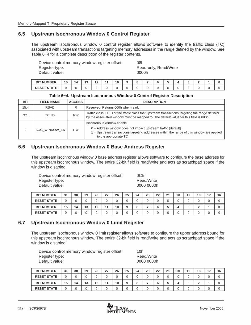
Memory-Mapped TI Proprietary Register Space
112 November 2005SCPS097B
6.5 Upstream Isochronous Window 0 Control Register
The upstream isochronous window 0 control register allows software to identify the traffic class (TC)associated with upstream transactions targeting memory addresses in the range defined by the window. SeeTable 6−4 for a complete description of the register contents.
Device control memory window register offset: 08hRegister type: Read-only, Read/WriteDefault value: 0000h
BIT NUMBER 15 14 13 12 11 10 9 8 7 6 5 4 3 2 1 0
RESET STATE 0 0 0 0 0 0 0 0 0 0 0 0 0 0 0 0
Table 6−4. Upstream Isochronous Window 0 Control Register DescriptionBIT FIELD NAME ACCESS DESCRIPTION
15:4 RSVD R Reserved. Returns 000h when read.
3:1 TC_ID RWTraffic class ID. ID of the traffic class that upstream transactions targeting the range definedby the associated window must be mapped to. The default value for this field is 000b.
0 ISOC_WINDOW_EN RW
Isochronous window enable.
0 = Address window does not impact upstream traffic (default)1 = Upstream transactions targeting addresses within the range of this window are applied
to the appropriate TC
6.6 Upstream Isochronous Window 0 Base Address Register
The upstream isochronous window 0 base address register allows software to configure the base address forthis upstream isochronous window. The entire 32-bit field is read/write and acts as scratchpad space if thewindow is disabled.
Device control memory window register offset: 0ChRegister type: Read/WriteDefault value: 0000 0000h
BIT NUMBER 31 30 29 28 27 26 25 24 23 22 21 20 19 18 17 16
RESET STATE 0 0 0 0 0 0 0 0 0 0 0 0 0 0 0 0
BIT NUMBER 15 14 13 12 11 10 9 8 7 6 5 4 3 2 1 0
RESET STATE 0 0 0 0 0 0 0 0 0 0 0 0 0 0 0 0
6.7 Upstream Isochronous Window 0 Limit Register
The upstream isochronous window 0 limit register allows software to configure the upper address bound forthis upstream isochronous window. The entire 32-bit field is read/write and acts as scratchpad space if thewindow is disabled.
Device control memory window register offset: 10hRegister type: Read/WriteDefault value: 0000 0000h
BIT NUMBER 31 30 29 28 27 26 25 24 23 22 21 20 19 18 17 16
RESET STATE 0 0 0 0 0 0 0 0 0 0 0 0 0 0 0 0
BIT NUMBER 15 14 13 12 11 10 9 8 7 6 5 4 3 2 1 0
RESET STATE 0 0 0 0 0 0 0 0 0 0 0 0 0 0 0 0

Memory-Mapped TI Proprietary Register Space
113November 2005 SCPS097B
6.8 Upstream Isochronous Window 1 Control Register
The upstream isochronous window 1 control register allows software to identify the TC associated withupstream transactions targeting memory addresses in the range defined by the window. See Table 6−5 fora complete description of the register contents.
Device control memory window register offset: 14hRegister type: Read-only, Read/WriteDefault value: 0000h
BIT NUMBER 15 14 13 12 11 10 9 8 7 6 5 4 3 2 1 0
RESET STATE 0 0 0 0 0 0 0 0 0 0 0 0 0 0 0 0
Table 6−5. Upstream Isochronous Window 1 Control Register DescriptionBIT FIELD NAME ACCESS DESCRIPTION
15:4 RSVD R Reserved. Returns 000h when read.
3:1 TC_ID RWTraffic class ID. ID of the traffic class that upstream transactions targeting the range definedby the associated window must be mapped to. The default value for this field is 000b.
0 ISOC_WINDOW_EN RW
Isochronous window enable.
0 = Address window does not impact upstream traffic (default)1 = Upstream transactions targeting addresses within the range of this window are
applied to the appropriate TC
6.9 Upstream Isochronous Window 1 Base Address Register
The upstream isochronous window 1 base address register allows software to configure the base address forthis upstream isochronous window. The entire 32-bit field is read/write and acts as scratchpad space if thewindow is disabled.
Device control memory window register offset: 18hRegister type: Read/WriteDefault value: 0000 0000h
BIT NUMBER 31 30 29 28 27 26 25 24 23 22 21 20 19 18 17 16
RESET STATE 0 0 0 0 0 0 0 0 0 0 0 0 0 0 0 0
BIT NUMBER 15 14 13 12 11 10 9 8 7 6 5 4 3 2 1 0
RESET STATE 0 0 0 0 0 0 0 0 0 0 0 0 0 0 0 0
6.10 Upstream Isochronous Window 1 Limit Register
The upstream isochronous window 1 limit register allows software to configure the upper address bound forthis upstream isochronous window. The entire 32-bit field is read/write and acts as scratchpad space if thewindow is disabled.
Device control memory window register offset: 1ChRegister type: Read/WriteDefault value: 0000 0000h
BIT NUMBER 31 30 29 28 27 26 25 24 23 22 21 20 19 18 17 16
RESET STATE 0 0 0 0 0 0 0 0 0 0 0 0 0 0 0 0
BIT NUMBER 15 14 13 12 11 10 9 8 7 6 5 4 3 2 1 0
RESET STATE 0 0 0 0 0 0 0 0 0 0 0 0 0 0 0 0
Memory-Mapped TI Proprietary Register Space
114 November 2005SCPS097B
6.11 Upstream Isochronous Window 2 Control Register
The upstream isochronous window 2 control register allows software to identify the TC associated withupstream transactions targeting memory addresses in the range defined by the window. See Table 6−6 fora complete description of the register contents.
Device control memory window register offset: 20hRegister type: Read-only, Read/WriteDefault value: 0000h
BIT NUMBER 15 14 13 12 11 10 9 8 7 6 5 4 3 2 1 0
RESET STATE 0 0 0 0 0 0 0 0 0 0 0 0 0 0 0 0
Table 6−6. Upstream Isochronous Window 2 Control Register DescriptionBIT FIELD NAME ACCESS DESCRIPTION
15:4 RSVD R Reserved. Returns 000h when read.
3:1 TC_ID RWTraffic class ID. ID of the traffic class that upstream transactions targeting the range definedby the associated window must be mapped to. The default value for this field is 000b.
0 ISOC_WINDOW_EN RW
Isochronous window enable.
0 = Address window does not impact upstream traffic (default)1 = Upstream transactions targeting addresses within the range of this window are
applied to the appropriate TC
6.12 Upstream Isochronous Window 2 Base Address Register
The upstream isochronous window 2 base address register allows software to configure the base address forthis upstream isochronous window. The entire 32-bit field is read/write and acts as scratchpad space if thewindow is disabled.
Device control memory window register offset: 24hRegister type: Read/WriteDefault value: 0000 0000h
BIT NUMBER 31 30 29 28 27 26 25 24 23 22 21 20 19 18 17 16
RESET STATE 0 0 0 0 0 0 0 0 0 0 0 0 0 0 0 0
BIT NUMBER 15 14 13 12 11 10 9 8 7 6 5 4 3 2 1 0
RESET STATE 0 0 0 0 0 0 0 0 0 0 0 0 0 0 0 0
6.13 Upstream Isochronous Window 2 Limit Register
The upstream isochronous window 2 limit register allows software to configure the upper address bound forthis upstream isochronous window. The entire 32-bit field is read/write and acts as scratchpad space if thewindow is disabled.
Device control memory window register offset: 28hRegister type: Read/WriteDefault value: 0000 0000h
BIT NUMBER 31 30 29 28 27 26 25 24 23 22 21 20 19 18 17 16
RESET STATE 0 0 0 0 0 0 0 0 0 0 0 0 0 0 0 0
BIT NUMBER 15 14 13 12 11 10 9 8 7 6 5 4 3 2 1 0
RESET STATE 0 0 0 0 0 0 0 0 0 0 0 0 0 0 0 0
Memory-Mapped TI Proprietary Register Space
115November 2005 SCPS097B
6.14 Upstream Isochronous Window 3 Control Register
The upstream isochronous window 3 control register allows software to identify the TC associated withupstream transactions targeting memory addresses in the range defined by the window. See Table 6−7 fora complete description of the register contents.
Device control memory window register offset: 2ChRegister type: Read-only, Read/WriteDefault value: 0000h
BIT NUMBER 15 14 13 12 11 10 9 8 7 6 5 4 3 2 1 0
RESET STATE 0 0 0 0 0 0 0 0 0 0 0 0 0 0 0 0
Table 6−7. Upstream Isochronous Window 3 Control Register DescriptionBIT FIELD NAME ACCESS DESCRIPTION
15:4 RSVD R Reserved. Returns 000h when read.
3:1 TC_ID RWTraffic class ID. ID of the traffic class that upstream transactions targeting the range definedby the associated window must be mapped to. The default value for this field is 000b.
0 ISOC_WINDOW_EN RW
Isochronous window enable.
0 = Address window does not impact upstream traffic (default)1 = Upstream transactions targeting addresses within the range of this window are
applied to the appropriate TC
6.15 Upstream Isochronous Window 3 Base Address Register
The upstream isochronous window 3 base address register allows software to configure the base address forthis upstream isochronous window. The entire 32-bit field is read/write and acts as scratchpad space if thewindow is disabled.
Device control memory window register offset: 30hRegister type: Read/WriteDefault value: 0000 0000h
BIT NUMBER 31 30 29 28 27 26 25 24 23 22 21 20 19 18 17 16
RESET STATE 0 0 0 0 0 0 0 0 0 0 0 0 0 0 0 0
BIT NUMBER 15 14 13 12 11 10 9 8 7 6 5 4 3 2 1 0
RESET STATE 0 0 0 0 0 0 0 0 0 0 0 0 0 0 0 0
6.16 Upstream Isochronous Window 3 Limit Register
The upstream isochronous window 3 limit register allows software to configure the upper address bound forthis upstream isochronous window. The entire 32-bit field is read/write and acts as scratchpad space if thewindow is disabled.
Device control memory window register offset: 34hRegister type: Read/WriteDefault value: 0000 0000h
BIT NUMBER 31 30 29 28 27 26 25 24 23 22 21 20 19 18 17 16
RESET STATE 0 0 0 0 0 0 0 0 0 0 0 0 0 0 0 0
BIT NUMBER 15 14 13 12 11 10 9 8 7 6 5 4 3 2 1 0
RESET STATE 0 0 0 0 0 0 0 0 0 0 0 0 0 0 0 0

Memory-Mapped TI Proprietary Register Space
116 November 2005SCPS097B
6.17 GPIO Control Register
This register controls the direction of the eight GPIO terminals. This register has no effect on the behavior ofGPIO terminals that are enabled to perform secondary functions. The secondary functions share GPIO0(CLKRUN), GPIO1 (PWR_OVRD), GPIO4 (SCL), and GPIO5 (SDA). This register is an alias of the GPIOcontrol register in the classic PCI configuration space (offset B4h, see Section 4.59). See Table 6−8 for acomplete description of the register contents.
Device control memory window register offset: 40hRegister type: Read-only, Read/WriteDefault value: 0000h
BIT NUMBER 15 14 13 12 11 10 9 8 7 6 5 4 3 2 1 0
RESET STATE 0 0 0 0 0 0 0 0 0 0 0 0 0 0 0 0
Table 6−8. GPIO Control Register DescriptionBIT FIELD NAME ACCESS DESCRIPTION
15:8 RSVD R Reserved. Returns 00h when read.
7† GPIO7_DIR RWGPIO 7 data direction. This bit selects whether GPIO7 is in input or output mode.
0 = Input (default)1 = Output
6† GPIO6_DIR RWGPIO 6 data direction. This bit selects whether GPIO6 is in input or output mode.
0 = Input (default)1 = Output
5† GPIO5_DIR RWGPIO 5 data direction. This bit selects whether GPIO5 is in input or output mode.
0 = Input (default)1 = Output
4† GPIO4_DIR RWGPIO 4 data direction. This bit selects whether GPIO4 is in input or output mode.
0 = Input (default)1 = Output
3† GPIO3_DIR RWGPIO 3 data direction. This bit selects whether GPIO3 is in input or output mode.
0 = Input (default)1 = Output
2† GPIO2_DIR RWGPIO 2 data direction. This bit selects whether GPIO2 is in input or output mode.
0 = Input (default)1 = Output
1† GPIO1_DIR RWGPIO 1 data direction. This bit selects whether GPIO1 is in input or output mode.
0 = Input (default)1 = Output
0† GPIO0_DIR RWGPIO 0 data direction. This bit selects whether GPIO0 is in input or output mode.
0 = Input (default)1 = Output
† These bits are reset by a PCI Express reset (PERST), a GRST, or the internally-generated power-on reset.
Memory-Mapped TI Proprietary Register Space
117November 2005 SCPS097B
6.18 GPIO Data Register
This register reads the state of the input mode GPIO terminals and changes the state of the output mode GPIOterminals. Writing to a bit that is in input mode or is enabled for a secondary function is ignored. The secondaryfunctions share GPIO0 (CLKRUN), GPIO1 (PWR_OVRD), GPIO4 (SCL), and GPIO5 (SDA). The defaultvalue at power up depends on the state of the GPIO terminals as they default to general-purpose inputs. Thisregister is an alias of the GPIO data register in the classic PCI configuration space (offset B6h, seeSection 4.60). See Table 6−9 for a complete description of the register contents.
Device control memory window register offset: 42hRegister type: Read-only, Read/WriteDefault value: 00XXh
BIT NUMBER 15 14 13 12 11 10 9 8 7 6 5 4 3 2 1 0
RESET STATE 0 0 0 0 0 0 0 0 x x x x x x x x
Table 6−9. GPIO Data Register DescriptionBIT FIELD NAME ACCESS DESCRIPTION
15:8 RSVD R Reserved. Returns 00h when read.
7† GPIO7_Data RWGPIO 7 data. This bit reads the state of GPIO7 when in input mode or changes the state ofGPIO7 when in output mode.
6† GPIO6_Data RWGPIO 6 data. This bit reads the state of GPIO6 when in input mode or changes the state ofGPIO6 when in output mode.
5† GPIO5_Data RWGPIO 5 data. This bit reads the state of GPIO5 when in input mode or changes the state ofGPIO5 when in output mode.
4† GPIO4_Data RWGPIO 4 data. This bit reads the state of GPIO4 when in input mode or changes the state ofGPIO4 when in output mode.
3† GPIO3_Data RWGPIO 3 data. This bit reads the state of GPIO3 when in input mode or changes the state ofGPIO3 when in output mode.
2† GPIO2_Data RWGPIO 2 data. This bit reads the state of GPIO2 when in input mode or changes the state ofGPIO2 when in output mode.
1† GPIO1_Data RWGPIO 1 data. This bit reads the state of GPIO1 when in input mode or changes the state ofGPIO1 when in output mode.
0† GPIO0_Data RWGPIO 0 data. This bit reads the state of GPIO0 when in input mode or changes the state ofGPIO0 when in output mode.
† These bits are reset by a PCI Express reset (PERST), a GRST, or the internally-generated power-on reset.
6.19 Serial-Bus Data Register
The serial-bus data register reads and writes data on the serial-bus interface. Write data is loaded into thisregister prior to writing the serial-bus slave address register that initiates the bus cycle. When reading datafrom the serial bus, this register contains the data read after bit 5 (REQBUSY) in the serial-bus control andstatus register (offset 47h, see Section 6.22) is cleared. This register is an alias for the serial-bus data registerin the PCI header (offset B0h, see Section 4.55). This register is reset by a PCI Express reset (PERST), aGRST, or the internally-generated power-on reset.
Device control memory window register offset: 44hRegister type: Read/WriteDefault value: 00h
BIT NUMBER 7 6 5 4 3 2 1 0
RESET STATE 0 0 0 0 0 0 0 0
Memory-Mapped TI Proprietary Register Space
118 November 2005SCPS097B
6.20 Serial-Bus Word Address Register
The value written to the serial-bus word address register represents the word address of the byte being readfrom or written to on the serial-bus interface. The word address is loaded into this register prior to writing theserial-bus slave address register that initiates the bus cycle. This register is an alias for the serial-bus wordaddress register in the PCI header (offset B1h, see Section 4.56). This register is reset by a PCI Express reset(PERST), a GRST, or the internally-generated power-on reset.
Device control memory window register offset: 45hRegister type: Read/WriteDefault value: 00h
BIT NUMBER 7 6 5 4 3 2 1 0
RESET STATE 0 0 0 0 0 0 0 0
6.21 Serial-Bus Slave Address Register
The serial-bus slave address register indicates the address of the device being targeted by the serial-buscycle. This register also indicates if the cycle will be a read or a write cycle. Writing to this register initiates thecycle on the serial interface. This register is an alias for the serial-bus slave address register in the PCI header(offset B2h, see Section 4.57). See Table 6−10 for a complete description of the register contents.
Device control memory window register offset: 46hRegister type: Read/WriteDefault value: 00h
BIT NUMBER 7 6 5 4 3 2 1 0
RESET STATE 0 0 0 0 0 0 0 0
Table 6−10. Serial-Bus Slave Address Register DescriptionBIT FIELD NAME ACCESS DESCRIPTION
7:1† SLAVE_ADDR RWSerial-bus slave address. This 7-bit field is the slave address for a serial-bus read or writetransaction. The default value for this field is 000 0000b.
0† RW_CMD RWRead/write command. This bit determines if the serial-bus cycle is a read or a write cycle.
0 = A single byte write is requested (default)1 = A single byte read is requested
† These bits are reset by a PCI Express reset (PERST), a GRST, or the internally-generated power-on reset.
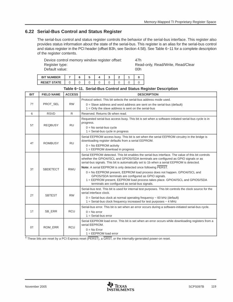
Memory-Mapped TI Proprietary Register Space
119November 2005 SCPS097B
6.22 Serial-Bus Control and Status Register
The serial-bus control and status register controls the behavior of the serial-bus interface. This register alsoprovides status information about the state of the serial-bus. This register is an alias for the serial-bus controland status register in the PCI header (offset B3h, see Section 4.58). See Table 6−11 for a complete descriptionof the register contents.
Device control memory window register offset: 47hRegister type: Read-only, Read/Write, Read/ClearDefault value: 00h
BIT NUMBER 7 6 5 4 3 2 1 0
RESET STATE 0 0 0 0 0 0 0 0
Table 6−11. Serial-Bus Control and Status Register DescriptionBIT FIELD NAME ACCESS DESCRIPTION
7† PROT_SEL RWProtocol select. This bit selects the serial-bus address mode used.
0 = Slave address and word address are sent on the serial-bus (default)1 = Only the slave address is sent on the serial-bus
6 RSVD R Reserved. Returns 0b when read.
5† REQBUSY RU
Requested serial-bus access busy. This bit is set when a software-initiated serial-bus cycle is inprogress.
0 = No serial-bus cycle1 = Serial-bus cycle in progress
4† ROMBUSY RU
Serial EEPROM access busy. This bit is set when the serial EEPROM circuitry in the bridge isdownloading register defaults from a serial EEPROM.
0 = No EEPROM activity1 = EEPROM download in progress
3† SBDETECT RWU
Serial EEPROM detected. This bit enables the serial-bus interface. The value of this bit controlswhether the GPIO4//SCL and GPIO5//SDA terminals are configured as GPIO signals or asserial-bus signals. This bit is automatically set to 1b when a serial EEPROM is detected.
Note: A serial EEPROM is only detected once following PERST.
0 = No EEPROM present, EEPROM load process does not happen. GPIO4//SCL and GPIO5//SDA terminals are configured as GPIO signals.
1 = EEPROM present, EEPROM load process takes place. GPIO4//SCL and GPIO5//SDA terminals are configured as serial-bus signals.
2† SBTEST RW
Serial-bus test. This bit is used for internal test purposes. This bit controls the clock source for theserial interface clock.
0 = Serial-bus clock at normal operating frequency ~ 60 kHz (default)1 = Serial-bus clock frequency increased for test purposes ~ 4 MHz
1† SB_ERR RCUSerial-bus error. This bit is set when an error occurs during a software-initiated serial-bus cycle.
0 = No error1 = Serial-bus error
0† ROM_ERR RCU
Serial EEPROM load error. This bit is set when an error occurs while downloading registers from aserial EEPROM.
0 = No Error1 = EEPROM load error
† These bits are reset by a PCI Express reset (PERST), a GRST, or the internally-generated power-on reset.
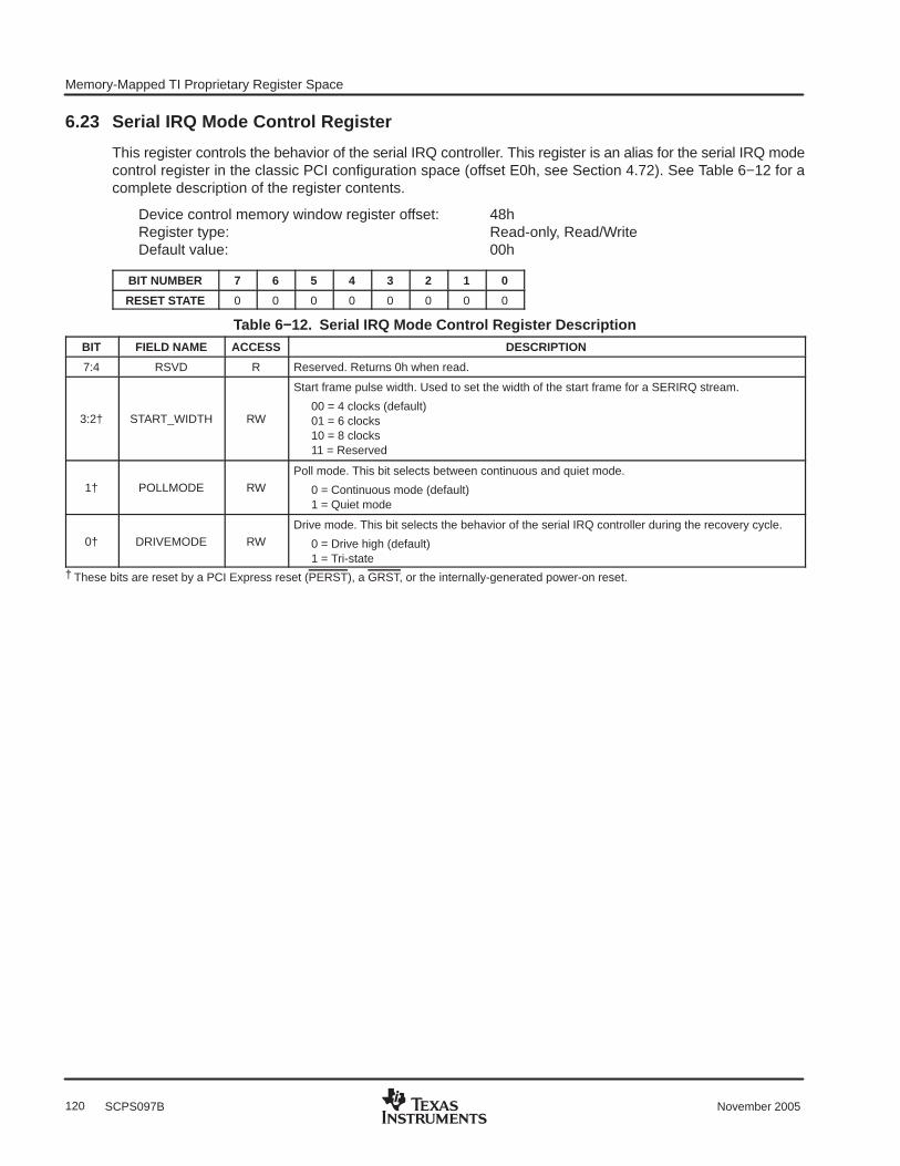
Memory-Mapped TI Proprietary Register Space
120 November 2005SCPS097B
6.23 Serial IRQ Mode Control Register
This register controls the behavior of the serial IRQ controller. This register is an alias for the serial IRQ modecontrol register in the classic PCI configuration space (offset E0h, see Section 4.72). See Table 6−12 for acomplete description of the register contents.
Device control memory window register offset: 48hRegister type: Read-only, Read/WriteDefault value: 00h
BIT NUMBER 7 6 5 4 3 2 1 0
RESET STATE 0 0 0 0 0 0 0 0
Table 6−12. Serial IRQ Mode Control Register DescriptionBIT FIELD NAME ACCESS DESCRIPTION
7:4 RSVD R Reserved. Returns 0h when read.
3:2† START_WIDTH RW
Start frame pulse width. Used to set the width of the start frame for a SERIRQ stream.
00 = 4 clocks (default)01 = 6 clocks10 = 8 clocks11 = Reserved
1† POLLMODE RWPoll mode. This bit selects between continuous and quiet mode.
0 = Continuous mode (default)1 = Quiet mode
0† DRIVEMODE RWDrive mode. This bit selects the behavior of the serial IRQ controller during the recovery cycle.
0 = Drive high (default)1 = Tri-state
† These bits are reset by a PCI Express reset (PERST), a GRST, or the internally-generated power-on reset.
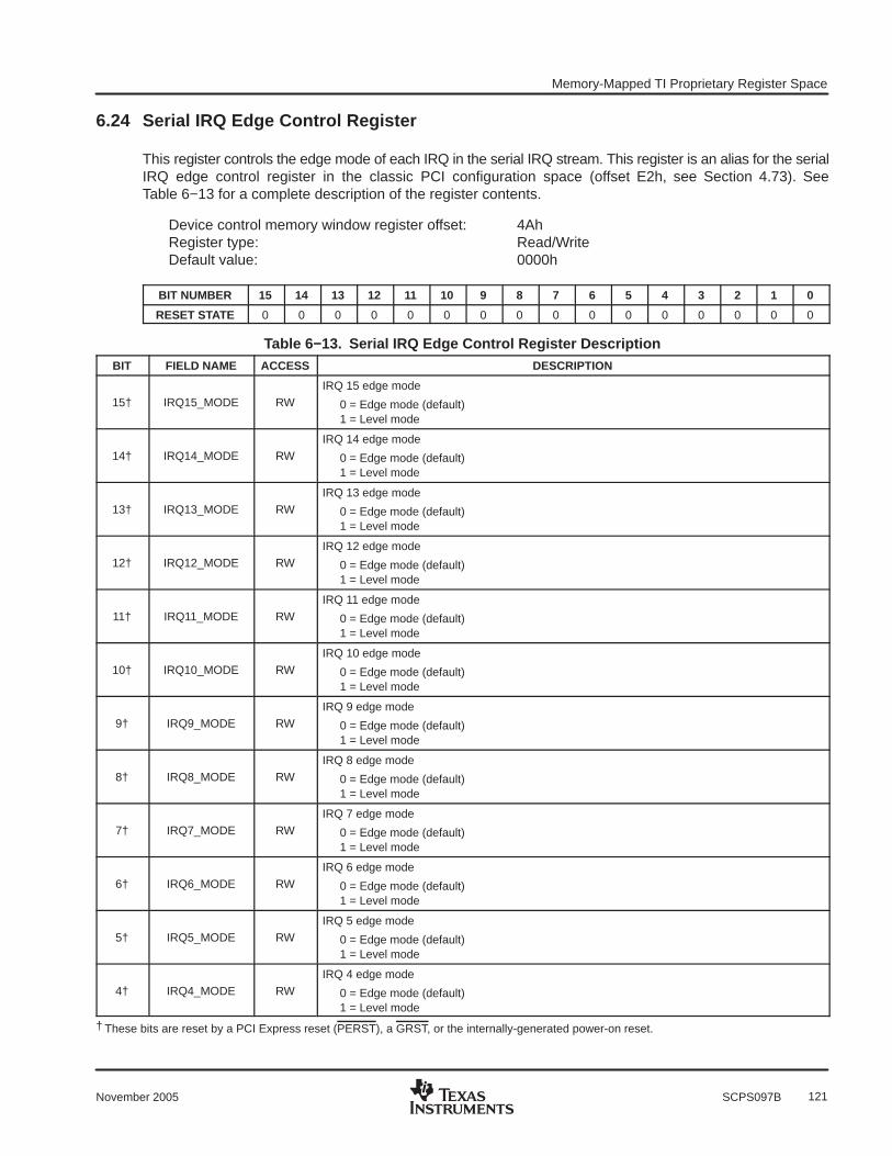
Memory-Mapped TI Proprietary Register Space
121November 2005 SCPS097B
6.24 Serial IRQ Edge Control Register
This register controls the edge mode of each IRQ in the serial IRQ stream. This register is an alias for the serialIRQ edge control register in the classic PCI configuration space (offset E2h, see Section 4.73). SeeTable 6−13 for a complete description of the register contents.
Device control memory window register offset: 4AhRegister type: Read/WriteDefault value: 0000h
BIT NUMBER 15 14 13 12 11 10 9 8 7 6 5 4 3 2 1 0
RESET STATE 0 0 0 0 0 0 0 0 0 0 0 0 0 0 0 0
Table 6−13. Serial IRQ Edge Control Register DescriptionBIT FIELD NAME ACCESS DESCRIPTION
15† IRQ15_MODE RWIRQ 15 edge mode
0 = Edge mode (default)1 = Level mode
14† IRQ14_MODE RWIRQ 14 edge mode
0 = Edge mode (default)1 = Level mode
13† IRQ13_MODE RWIRQ 13 edge mode
0 = Edge mode (default)1 = Level mode
12† IRQ12_MODE RWIRQ 12 edge mode
0 = Edge mode (default)1 = Level mode
11† IRQ11_MODE RWIRQ 11 edge mode
0 = Edge mode (default)1 = Level mode
10† IRQ10_MODE RWIRQ 10 edge mode
0 = Edge mode (default)1 = Level mode
9† IRQ9_MODE RWIRQ 9 edge mode
0 = Edge mode (default)1 = Level mode
8† IRQ8_MODE RWIRQ 8 edge mode
0 = Edge mode (default)1 = Level mode
7† IRQ7_MODE RWIRQ 7 edge mode
0 = Edge mode (default)1 = Level mode
6† IRQ6_MODE RWIRQ 6 edge mode
0 = Edge mode (default)1 = Level mode
5† IRQ5_MODE RWIRQ 5 edge mode
0 = Edge mode (default)1 = Level mode
4† IRQ4_MODE RWIRQ 4 edge mode
0 = Edge mode (default)1 = Level mode
† These bits are reset by a PCI Express reset (PERST), a GRST, or the internally-generated power-on reset.

Memory-Mapped TI Proprietary Register Space
122 November 2005SCPS097B
Table 6−13. Serial IRQ Edge Control Register Description (Continued)BIT FIELD NAME ACCESS DESCRIPTION
3† IRQ3_MODE RWIRQ 3 edge mode
0 = Edge mode (default)1 = Level mode
2† IRQ2_MODE RWIRQ 2 edge mode
0 = Edge mode (default)1 = Level mode
1† IRQ1_MODE RWIRQ 1 edge mode
0 = Edge mode (default)1 = Level mode
0† IRQ0_MODE RWIRQ 0 edge mode
0 = Edge mode (default)1 = Level mode
† These bits are reset by a PCI Express reset (PERST), a GRST, or the internally-generated power-on reset.
6.25 Serial IRQ Status RegisterThis register indicates when a level mode IRQ is signaled on the serial IRQ stream. After a level mode IRQis signaled, a write-back of 1b to the asserted IRQ status bit re-arms the interrupt. IRQ interrupts that aredefined as edge mode in the serial IRQ edge control register are not reported in this status register.
This register is an alias for the serial IRQ status register in the classic PCI configuration space (offset E4h,see Section 4.74). See Table 6−14 for a complete description of the register contents.
Device control memory window register offset: 4ChRegister type: Read/ClearDefault value: 0000h
BIT NUMBER 15 14 13 12 11 10 9 8 7 6 5 4 3 2 1 0
RESET STATE 0 0 0 0 0 0 0 0 0 0 0 0 0 0 0 0
Table 6−14. Serial IRQ Status Register DescriptionBIT FIELD NAME ACCESS DESCRIPTION
15 IRQ15 RCUIRQ 15 asserted. This bit indicates that the IRQ has been asserted.
0 = Deasserted1 = Asserted
14 IRQ14 RCUIRQ 14 asserted. This bit indicates that the IRQ has been asserted.
0 = Deasserted1 = Asserted
13 IRQ13 RCUIRQ 13 asserted. This bit indicates that the IRQ has been asserted.
0 = Deasserted1 = Asserted
12 IRQ12 RCUIRQ 12 asserted. This bit indicates that the IRQ has been asserted.
0 = Deasserted1 = Asserted
11 IRQ11 RCUIRQ 11 asserted. This bit indicates that the IRQ has been asserted.
0 = Deasserted1 = Asserted
10 IRQ10 RCUIRQ 10 asserted. This bit indicates that the IRQ has been asserted.
0 = Deasserted1 = Asserted
9 IRQ9 RCUIRQ 9 asserted. This bit indicates that the IRQ has been asserted.
0 = Deasserted1 = Asserted

Memory-Mapped TI Proprietary Register Space
123November 2005 SCPS097B
Table 6−14. Serial IRQ Status Register Description (Continued)BIT FIELD NAME ACCESS DESCRIPTION
8 IRQ8 RCUIRQ 8 asserted. This bit indicates that the IRQ has been asserted.
0 = Deasserted1 = Asserted
7 IRQ7 RCUIRQ 7 asserted. This bit indicates that the IRQ has been asserted.
0 = Deasserted1 = Asserted
6 IRQ6 RCUIRQ 6 asserted. This bit indicates that the IRQ has been asserted.
0 = Deasserted1 = Asserted
5 IRQ5 RCUIRQ 5 asserted. This bit indicates that the IRQ has been asserted.
0 = Deasserted1 = Asserted
4 IRQ4 RCUIRQ 4 asserted. This bit indicates that the IRQ has been asserted.
0 = Deasserted1 = Asserted
3 IRQ3 RCUIRQ 3 asserted. This bit indicates that the IRQ has been asserted.
0 = Deasserted1 = Asserted
2 IRQ2 RCUIRQ 2 asserted. This bit indicates that the IRQ has been asserted.
0 = Deasserted1 = Asserted
1 IRQ1 RCUIRQ 1 asserted. This bit indicates that the IRQ has been asserted.
0 = Deasserted1 = Asserted
0 IRQ0 RCUIRQ 0 asserted. This bit indicates that the IRQ has been asserted.
0 = Deasserted1 = Asserted

Electrical Characteristics
124 November 2005SCPS097B
7 Electrical Characteristics
7.1 Absolute Maximum Ratings Over Operating Temperature Ranges †
Supply voltage range: VDD_33 –0.5 V to 3.6 V. . . . . . . . . . . . . . . . . . . . . . . . . . . . . . . . . . . . . . . . . . . . . . . . . . VDD_15 –0.5 V to 1.65 V. . . . . . . . . . . . . . . . . . . . . . . . . . . . . . . . . . . . . . . . . . . . . . . . . VCCP –0.5 V to 5.25 V. . . . . . . . . . . . . . . . . . . . . . . . . . . . . . . . . . . . . . . . . . . . . . . . . .
Input voltage range, VI: PCI –0.5 V to VCCP + 0.5 V. . . . . . . . . . . . . . . . . . . . . . . . . . . . . . . . . . . . . . . . . . VI: PCI Express (RX) –0.6 V to 0.6 V. . . . . . . . . . . . . . . . . . . . . . . . . . . . . . . . . . . . . . VI: PCI Express REFCLK (single-ended) –0.5 V toVDD_33 + 0.5 V. . . . . . . . . . . . VI: PCI Express REFCLK (differential) –0.5 V toVDD_15 + 0.5 V. . . . . . . . . . . . . . VI: Miscellaneous 3.3-V IO –0.5 V to VDD_33 + 0.5 V. . . . . . . . . . . . . . . . . . . . . . . .
Output voltage range: VO: PCI –0.5 V to VDD_33 + 0.5 V. . . . . . . . . . . . . . . . . . . . . . . . . . . . . . . . . . . . . . . VO: PCI Express (TX) –0.5 V to VDD_15 + 0.5V. . . . . . . . . . . . . . . . . . . . . . . . . . . . VO: Miscellaneous 3.3-V IO –0.5 V to VDD_33 + 0.5 V. . . . . . . . . . . . . . . . . . . . . .
Input clamp current, (VI < 0 or VI > VDD) (see Note 1) ±20 mA. . . . . . . . . . . . . . . . . . . . . . . . . . . . . . . . . . . . . Output clamp current, (VO < 0 or VO > VDD) (see Note 2) ±20 mA. . . . . . . . . . . . . . . . . . . . . . . . . . . . . . . . . Human body model (HBM) ESD performance 1500 V. . . . . . . . . . . . . . . . . . . . . . . . . . . . . . . . . . . . . . . . . . . . Charged device model (CDM) ESD performance 500 V. . . . . . . . . . . . . . . . . . . . . . . . . . . . . . . . . . . . . . . . . . Storage temperature range, Tstg –65°C to 150°C. . . . . . . . . . . . . . . . . . . . . . . . . . . . . . . . . . . . . . . . . . . . . . . . † Stresses beyond those listed under absolute maximum ratings may cause permanent damage to the device. These are stress ratings
only, and functional operation of the device at these or any other conditions beyond those indicated under recommended operatingconditions is not implied. Exposure to absolute-maximum-rated conditions for extended periods may affect device reliability.
NOTES: 1. Applies for external input and bidirectional buffers. VI < 0 or VI > VDD or VI > VCCP.2. Applies to external output and bidirectional buffers. VO < 0 or VO > VDD or VO > VCCP.
7.2 Recommended Operation Conditions
OPERATION MIN NOM MAX UNITS
VDD_15Supply voltage 1.5 V 1.35 1.5 1.65 V
VDDA_15Supply voltage 1.5 V 1.35 1.5 1.65 V
VDD_33VDDA_33 Supply voltage 3.3 V 3 3.3 3.6 V
VDDA_33_AUX
Supply voltage 3.3 V 3 3.3 3.6 V
VCCP PCI bus clamping rail voltage3.3 V 3 3.3 3.6
VVCCP PCI bus clamping rail voltage5.0 V 4.75 5 5.25
V
TA Operating ambient temperature range 0 25 70 C
TJ Virtual junction temperature (Note 3) 0 25 115 C
NOTE 3: The junction temperature reflects simulated conditions. The customer is responsible for verifying junction temperature.

Electrical Characteristics
125November 2005 SCPS097B
7.3 PCI Express Differential Transmitter Output Ranges
PARAMETER TERMINALS MIN NOM MAX UNITS COMMENTS
UI
Unit intervalTXP, TXN 399.88 400 400.12 ps
Each UI is 400 ps ±300 ppm. UI does not account forSSC dictated variations.
See Note 4.
VTX-DIFFp-p Differentialpeak-to-peak outputvoltage
TXP, TXN 0.8 1.2 VVTX-DIFFp-p = 2*|VTXP − VTXN|
See Note 5.
VTX-DE-RATIODe-emphasizeddifferential outputvoltage (ratio)
TXP, TXN −3.0 −3.5 −4.0 dB
This is the ratio of the VTX-DIFFp-p of the second andfollowing bits after a transition divided by the VTX-DIFFp-pof the first bit after a transition.
See Note 5.
TTX-EYE Minimum TX eye width
TXP, TXN 0.75 UIThe maximum transmitter jitter can be derived asTTXMAX- JITTER = 1 − TTX-EYE = 0.3 UI
See Notes 5 and 6.
TTX-EYE-MEDIAN-to-MAX-JITTER Maximum time betweenthe jitter median andmaximum deviationfrom the median
TXP, TXN 0.15 UI
Jitter is defined as the measurement variation of thecrossing points (VTX-DIFFp-p = 0 V) in relation torecovered TX UI. A recovered TX UI is calculated over3500 consecutive UIs of sample data. Jitter is measuredusing all edges of the 250 consecutive UIs in the centerof the 3500 UIs used for calculating the TX UI.
See Notes 5 and 6.
TTX-RISE,TTX-FALLP/N TX output rise/falltime
TXP, TXN 0.125 UI See Notes 5 and 8.
VTX-CM-ACpRMS ac peak commonmode output voltage
TXP, TXN 20 mV
VTX-CM-ACp = RMS(|VTXP + VTXN|/2 – VTX-CM-DC)
VTX-CM-DC = DC(avg) of |VTXP + VTXN|/2
See Note 5.
VTX-CM-DC-ACTIVE-IDLE-DELTAAbsolute delta of dccommon mode voltageduring L0 and electricalidle
TXP, TXN 0 100 mV
|VTX-CM-DC – VTX-CM-Idle-DC| 100 mV
VTX-CM-DC = DC(avg) of |VTXP + VTXN|/2 [during L0]
VTX-CM-Idle-DC = DC(avg) of |VTXP + VTXN|/2 [duringelectrical idle]
See Note 5.
VTX-CM-DC-LINE-DELTAAbsolute delta of dccommon mode voltagebetween P and N
TXP, TXN 0 25 mV
|VTXP-CM-DC – VTXN-CM-DC| 25 mV when
VTXP-CM-DC = DC(avg) of |VTXP| VTXN-CM-DC = DC(avg) of |VTXN|
See Note 5.
VTX-IDLE-DIFFpElectrical idledifferential peak outputvoltage
TXP, TXN 0 20 mVVTX-IDLE-DIFFp = |VTXP-Idle − VTXN-Idle| 20 mV
See Note 5.
VTX-RCV-DETECTThe amount of voltagechange allowed duringreceiver detection
TXP, TXN 600 mVThe total amount of voltage change that a transmittercan apply to sense whether a low impedance receiver ispresent.
VTX-DC-CMThe TX dc commonmode voltage
TXP, TXN 0 3.6 VThe allowed dc common mode voltage under anycondition

Electrical Characteristics
126 November 2005SCPS097B
PCI Express Differential Transmitter Output Ranges (continued)
PARAMETER TERMINALS MIN NOM MAX UNITS COMMENTS
ITX-SHORTTX short circuit currentlimit
TXP, TXN 90 mAThe total current the transmitter can provide whenshorted to its ground.
TTX-IDLE-MINMinimum time spent inelectrical idle
TXP, TXN 50 UI
Minimum time a transmitter must be in electrical idle.Utilized by the receiver to start looking for an electricalidle exit after successfully receiving an electrical idleordered set.
TTX-IDLE-SET-to-IDLEMaximum time totransition to a validelectrical idle aftersending an electricalidle ordered set
TXP, TXN 20 UI
After sending an electrical idle ordered set, thetransmitter must meet all electrical idle specificationswithin this time. This is considered a debounce time forthe transmitter to meet electrical idle after transitioningfrom L0.
TTX-IDLE-to-DIFF-DATAMaximum time totransition to valid TXspecifications afterleaving an electrical idlecondition
TXP, TXN 20 UI
Maximum time to meet all TX specifications whentransitioning from electrical idle to sending differentialdata. This is considered a debounce time for the TX tomeet all TX specifications after leaving electrical idle.
RLTX-DIFFDifferential return loss
TXP, TXN 10 dB Measured over 50 MHz to 1.25 GHz. See Note 7.
RLTX-CMCommon mode returnloss
TXP, TXN 6 dB Measured over 50 MHz to 1.25 GHz. See Note 7.
ZTX-DIFF-DCDC differential TXimpedance
TXP, TXN 80 100 120 Ω TX dc differential mode low impedance
ZTX-DCTransmitter dcimpedance
TXP, TXN 40 ΩRequired TXP as well as TXN dc impedance during allstates
CTXAC coupling capacitor
TXP, TXN 75 200 nFAll transmitters are ac-coupled and are required on thePWB.
NOTES: 4. No test load is necessarily associated with this value.5. Specified at the measurement point into a timing and voltage compliance test load and measured over any 250 consecutive TX UIs.6. A TTX-EYE = 0.75 UI provides for a total sum of deterministic and random jitter budget of TTX-JITTER-MAX = 0.25 UI for the transmitter
collected over any 250 consecutive TX UIs. The TTX-EYE-MEDIAN-to-MAX-JITTER specification ensures a jitter distribution in which themedian and the maximum deviation from the median is less than half of the total TX jitter budget collected over any 250 consecutiveTX UIs. It must be noted that the median is not the same as the mean. The jitter median describes the point in time where the numberof jitter points on either side is approximately equal as opposed to the averaged time value.
7. The transmitter input impedance results in a differential return loss greater than or equal to 12 dB and a common mode return lossgreater than or equal to 6 dB over a frequency range of 50 MHz to 1.25 GHz. This input impedance requirement applies to all validinput levels. The reference impedance for return loss measurements is 50 Ω to ground for both the P and N line. Note that the seriescapacitors CTX is optional for the return loss measurement.
8. Measured between 20% and 80% at transmitter package terminals into a test load for both VTXP and VTXN.

Electrical Characteristics
127November 2005 SCPS097B
7.4 PCI Express Differential Receiver Input Ranges
PARAMETER TERMINALS MIN NOM MAX UNITS COMMENTS
UI
Unit intervalRXP, RXN 399.88 400 400.12 ps
Each UI is 400 ps ±300 ppm. UI does not account for SSCdictated variations.
See Note 9.
VRX-DIFFp-pDifferential inputpeak-to-peak voltage
RXP, RXN 0.175 1.200 VVRX-DIFFp-p = 2*|VRXP − VRXN|
See Note 10.
TRX-EYEMinimum receiver eyewidth
RXP, RXN 0.4 UI
The maximum interconnect media and transmitter jitter thatcan be tolerated by the receiver is derived as TRX-MAX- JITTER = 1 − TRX-EYE = 0.6 UI
See Notes 10 and 11.
TRX-EYE-MEDIAN-to-MAX-JITTERMaximum time betweenthe jitter median andmaximum deviationfrom the median.
RXP, RXN 0.3 UI
Jitter is defined as the measurement variation of thecrossing points (VRX-DIFFp-p = 0 V) in relation to recoveredTX UI. A recovered TX UI is calculated over3500 consecutive UIs of sample data. Jitter is measuredusing all edges of the 250 consecutive UIs in the center ofthe 3500 UIs used for calculating the TX UI.
See Notes 10 and 11.
VRX-CM-ACpAC peak common modeinput voltage
RXP, RXN 150 mV
VRX-CM-ACp = RMS(|VRXP + VRXN|/2 – VRX-CM-DC)
VRX-CM-DC = DC(avg) of |VRXP + VRXN|/2
See Note 10.
RLRX-DIFFDifferential return loss
RXP, RXN 10 dBMeasured over 50 MHz to 1.25 GHz with the P and N linesbiased at +300 mV and −300 mV, respectively.
See Note 12.
RLRX-CMCommon mode returnloss
RXP, RXN 6 dBMeasured over 50 MHz to 1.25 GHz with the P and N linesbiased at +300 mV and −300 mV, respectively.
See Note 12.
ZRX-DIFF-DCDC differential inputimpedance
RXP, RXN 80 100 120 ΩRX dc differential mode impedance
See Note 13.
ZRX-DCDC input impedance
RXP, RXN 40 50 60 ΩRequired RXP as well as RXN dc impedance (50 Ω ±20%tolerance)
See Notes 10 and 13.
ZRX-HIGH-IMP-DCPowered down dc inputimpedance
RXP, RXN 200K ΩRequired RXP as well as RXN dc impedance when thereceiver terminations do not have power.
See Note 14.
VRX-IDLE-DET-DIFFp-pElectrical idle detectthreshold
RXP, RXN 65 175 mVVRX-IDLE-DET-DIFFp-p = 2 * |VRXP − VRXN| measured at thereceiver package terminals
TRX-IDLE-DET-DIFF-ENTER-TIMEUnexpected electricalidle enter detectthreshold integrationtime
RXP, RXN 10 ms
An unexpected electrical idle (VRX-DIFFp-p < VRX-IDLE-DET-DIFFp-p) must be recognized nolonger than TRX-IDLE-DET-DIFF-ENTER-TIME to signal anunexpected idle condition.
NOTES: 9. No test load is necessarily associated with this value.10. Specified at the measurement point and measured over any 250 consecutive UIs. A test load must be used as the RX device when
taking measurements. If the clocks to the RX and TX are not derived from the same reference clock, then the TX UI recovered from3500 consecutive UIs is used as a reference for the eye diagram.

Electrical Characteristics
128 November 2005SCPS097B
11. A TRX-EYE = 0.40 UI provides for a total sum of 0.60 UI deterministic and random jitter budget for the transmitter and interconnectcollected any 250 consecutive UIs. The TRX-EYE-MEDIAN-to-MAX-JITTER specification ensures a jitter distribution in which the medianand the maximum deviation from the median is less than half of the total UI jitter budget collected over any 250 consecutive TX UIs.It must be noted that the median is not the same as the mean. The jitter median describes the point in time where the number ofjitter points on either side is approximately equal as opposed to the averaged time value. If the clocks to the RX and TX are not derivedfrom the same reference clock, then the TX UI recovered from 3500 consecutive UIs must be used as the reference for the eyediagram.
12. The receiver input impedance results in a differential return loss greater than or equal to 15 dB with the P line biased to 300 mV andthe N line biased to −300 mV and a common mode return loss greater than or equal to 6 dB (no bias required) over a frequency rangeof 50 MHz to 1.25 GHz. This input impedance requirement applies to all valid input levels. The reference impedance for return lossmeasurements for is 50 Ω to ground for both the P and N line (i.e., as measured by a Vector Network Analyzer with 50-Ω probes).The series capacitors CTX is optional for the return loss measurement.
13. Impedance during all link training status state machine (LTSSM) states. When transitioning from a PCI Express reset to the detectstate (the initial state of the LTSSM) there is a 5-ms transition time before receiver termination values must be met on theunconfigured lane of a port.
14. The RX dc common mode impedance that exists when no power is present or PCI Express reset is asserted. This helps ensure thatthe receiver detect circuit does not falsely assume a receiver is powered on when it is not. This term must be measured at 300 mVabove the RX ground.

Electrical Characteristics
129November 2005 SCPS097B
7.5 PCI Express Differential Reference Clock Input Ranges
PARAMETER TERMINALS MIN NOM MAX UNITS COMMENTS
fIN-DIFFDifferential inputfrequency
REFCLK+
REFCLK−100 MHz
The input frequency is 100 MHz + 300 ppm and− 2800 ppm including SSC-dictated variations.
fIN-SESingle-ended inputfrequency
REFCLK+ 125 MHz The input frequency is 125 MHz ± 300 ppm.
VRX-DIFFp-pDifferential inputpeak-to-peak voltage
REFCLK+
REFCLK−0.175 1.200 V VRX-DIFFp-p = 2*|VREFCLK+ − VREFCLK−|
VIH-SE REFCLK+ 0.7VDDA_33 VDDA_33 VSingle-ended, reference clock mode high-levelinput voltage
VIL-SE REFCLK+ 0 0.3VDDA_33 VSingle-ended, reference clock mode low-levelinput voltage
VRX-CM-ACpAC peak commonmode input voltage
REFCLK+
REFCLK−140 mV
VRX-CM-ACp = RMS( |VREFCLK+ + VREFCLK−|/2 –VRX-CM-DC)
VRX-CM-DC = DC(avg) of |VREFCLK+ + VREFCLK−|/2
Duty cycleREFCLK+
REFCLK−40% 60%
Differential and single-ended waveform inputduty cycle
ZRX-DIFF-DCDC differential inputimpedance
REFCLK+
REFCLK−20 kΩ REFCLK+/− dc differential mode impedance
ZRX-DCDC input impedance
REFCLK+
REFCLK−20 kΩ REFCLK+ dc single-ended mode impedance
NOTE 15: The XIO2000 is compliant with the defined system jitter models for a PCI-Express reference clock and associated TX/RX link. Thesesystem jitter models are described in the PCI-Express Jitter Modeling, Revision 1.0RD document. Any usage of the XIO2000 in a systemconfiguration that does not conform to the defined system jitter models requires the system designer to validate the system jitter budgets.

Electrical Characteristics
130 November 2005SCPS097B
7.6 Electrical Characteristics Over Recommended Operating Conditions (PCI Bus)
PARAMETER OPERATIONTEST
CONDITIONS MIN MAX UNITS
VIH High-level input voltage (Note 16)VCCP = 3.3 V 0.5 VDD_33 VCCP
VVIH High-level input voltage (Note 16)VCCP = 5.0 V 0.5 VDD_33 VCCP
V
VIL Low-level input voltage (Note 16)VCCP = 3.3 V 0 0.3 VDD_33
VVIL Low-level input voltage (Note 16)VCCP = 5.0 V 0 0.3 VDD_33
V
VI Input voltage 0 VCCP V
VO Output voltage (Note 17) 0 VDD_33 V
tt Input transition time (trise and tfall) 1 4 ns
VOH High-level output voltage (Note 17) VDD_33 IOH = −32 mA 0.7 VDD_33 V
VOL Low-level output voltage (Note 17) VDD_33 IOL = 32 mA 0.18 VDD_33 V
IOZ High-impedance, output current (Note 17)VCCP = 3.3 V VI = 0 to VCCP ±10
AIOZ High-impedance, output current (Note 17)VCCP = 5.0 V VI = 0 to VCCP ±70
µA
II Input current (Note 16)VCCP = 3.3 V VI = 0 to VCCP ±10
AII Input current (Note 16)VCCP = 5.0 V VI = 0 to VCCP ±70
µA
NOTES: 16. Applies to external inputs and bidirectional buffers.17. Applies to external outputs and bidirectional buffers.
Note: This table applies to CLK, CLKOUT6:0, AD31:0, C/BE[3:0], DEVSEL, FRAME, GNT5:0, INTD:A,IRDY, PAR, PERR, REQ5:0, PRST, SERR, STOP, TRDY, SERIRQ, M66EN, and LOCK terminals.
7.7 Electrical Characteristics Over Recommended Operating Conditions (3.3-V I/O)
PARAMETER OPERATIONTEST
CONDITIONS MIN MAX UNITS
VIH High-level input voltage (Note 18) VDD_33 0.7 VDD_33 VDD_33 V
VIL Low-level input voltage (Note 18) VDD_33 0 0.3 VDD_33 V
VI Input voltage 0 VDD_33 V
VO Output voltage (Note 19) 0 VDD_33 V
tt Input transition time (trise and tfall) 0 25 ns
Vhys Input hysteresis (Note 21) 0.13 VDD_33 V
VOH High-level output voltage VDD_33 IOH = −4 mA 0.8 VDD_33 V
VOL Low-level output voltage VDD_33 IOL = 4 mA 0.22 VDD_33 V
IOZ High-impedance, output current (Note 19) VDD_33 VI = 0 to VDD_33 ±20 µA
IOZPHigh-impedance, output current with internal pullup orpulldown (Note 22)
VDD_33 VI = 0 to VDD_33 ±100 µA
II Input current (Note 20) VDD_33 VI = 0 to VDD_33 ±1 µA
NOTES: 18. Applies to external inputs and bidirectional buffers.19. Applies to external outputs and bidirectional buffers.20. Applies to external input buffers.21. Applies to PERST, GRST, and PME.22. Applies to GRST (pullup), EXT_ARB_EN (pulldown), CLKRUN_EN (pulldown), and most GPIO (pullup).
Note: This table applies to PERST, WAKE, REFCLK_SEL, PME, CLKRUN_EN, EXT_ARB_EN, GRST,GPIO7:0, and all RSVD input terminals.
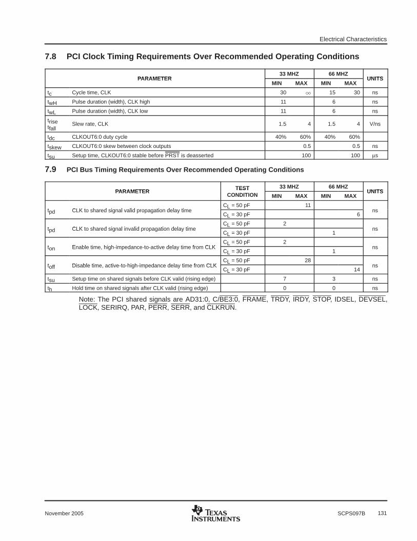
Electrical Characteristics
131November 2005 SCPS097B
7.8 PCI Clock Timing Requirements Over Recommended Operating Conditions
PARAMETER33 MHZ 66 MHZ
UNITSPARAMETERMIN MAX MIN MAX
UNITS
tc Cycle time, CLK 30 15 30 ns
twH Pulse duration (width), CLK high 11 6 ns
twL Pulse duration (width), CLK low 11 6 ns
trise tfall
Slew rate, CLK 1.5 4 1.5 4 V/ns
tdc CLKOUT6:0 duty cycle 40% 60% 40% 60%
tskew CLKOUT6:0 skew between clock outputs 0.5 0.5 ns
tsu Setup time, CLKOUT6:0 stable before PRST is deasserted 100 100 µs
7.9 PCI Bus Timing Requirements Over Recommended Operating Conditions
PARAMETERTEST 33 MHZ 66 MHZ
UNITSPARAMETERTEST
CONDITION MIN MAX MIN MAXUNITS
tpd CLK to shared signal valid propagation delay timeCL = 50 pF 11
nstpd CLK to shared signal valid propagation delay timeCL = 30 pF 6
ns
tpd CLK to shared signal invalid propagation delay timeCL = 50 pF 2
nstpd CLK to shared signal invalid propagation delay timeCL = 30 pF 1
ns
ton Enable time, high-impedance-to-active delay time from CLKCL = 50 pF 2
nston Enable time, high-impedance-to-active delay time from CLKCL = 30 pF 1
ns
toff Disable time, active-to-high-impedance delay time from CLKCL = 50 pF 28
nstoff Disable time, active-to-high-impedance delay time from CLKCL = 30 pF 14
ns
tsu Setup time on shared signals before CLK valid (rising edge) 7 3 ns
th Hold time on shared signals after CLK valid (rising edge) 0 0 ns
Note: The PCI shared signals are AD31:0, C/BE3:0, FRAME, TRDY, IRDY, STOP, IDSEL, DEVSEL,LOCK, SERIRQ, PAR, PERR, SERR, and CLKRUN.
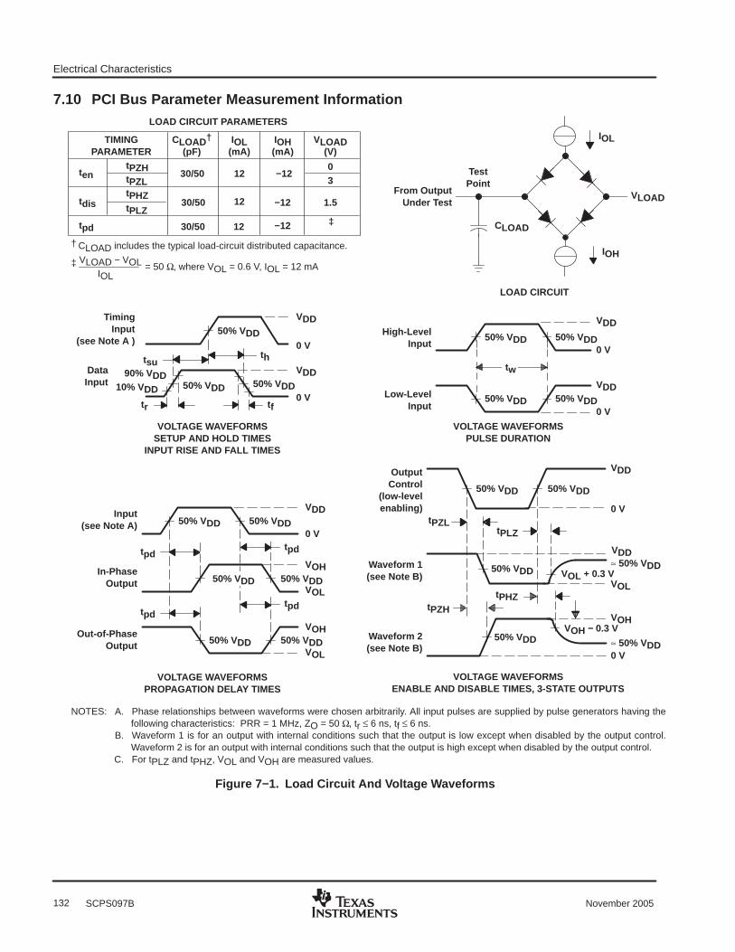
Electrical Characteristics
132 November 2005SCPS097B
7.10 PCI Bus Parameter Measurement Information
† CLOAD includes the typical load-circuit distributed capacitance.
CLOAD
TestPoint
TimingInput
(see Note A )
Out-of-PhaseOutput
tpd
50% VDD
50% VDD
VDD
0 V
0 V
0 V
0 V
0 V
VOL
thtsu
VOH
VOH
VOL
High-LevelInput
Low-LevelInput
tw
VOLTAGE WAVEFORMSPROPAGATION DELAY TIMES
LOAD CIRCUIT
VOLTAGE WAVEFORMSSETUP AND HOLD TIMES
INPUT RISE AND FALL TIMES
VOLTAGE WAVEFORMSPULSE DURATION
tpdtpd
tpd
VLOAD
IOH
IOL
From Output Under Test
90% VDD10% VDD
tftr
OutputControl
(low-levelenabling)
Waveform 1(see Note B)
Waveform 2(see Note B)
VOL
VOHVOH − 0.3 V
tPZL
tPZH
tPLZ
tPHZ
VOLTAGE WAVEFORMSENABLE AND DISABLE TIMES, 3-STATE OUTPUTS
VOL + 0.3 V
0 V
0 V
≈ 50% VDD
≈ 50% VDD
ten
tdis
tpd
tPZHtPZLtPHZtPLZ
CLOAD†
(pF)IOL
(mA)TIMING
PARAMETER
30/50 12 −12
03
1.5
‡30/50 12
12
−12
−12
LOAD CIRCUIT PARAMETERS
= 50 Ω, where VOL = 0.6 V, IOL = 12 mAIOL
30/50
‡ VLOAD − VOL
IOH(mA)
VLOAD(V)
DataInput
In-PhaseOutput
Input(see Note A)
VDD
VDD
VDD50% VDD
50% VDD 50% VDD
50% VDD
VDD
VDD
50% VDD 50% VDD
50% VDD
50% VDD
VDD50% VDD 50% VDD
50% VDD 50% VDD
50% VDD 50% VDD
NOTES: A. Phase relationships between waveforms were chosen arbitrarily. All input pulses are supplied by pulse generators having thefollowing characteristics: PRR = 1 MHz, ZO = 50 Ω, tr ≤ 6 ns, tf ≤ 6 ns.
B. Waveform 1 is for an output with internal conditions such that the output is low except when disabled by the output control.Waveform 2 is for an output with internal conditions such that the output is high except when disabled by the output control.
C. For tPLZ and tPHZ, VOL and VOH are measured values.
50% VDD
Figure 7−1. Load Circuit And Voltage Waveforms
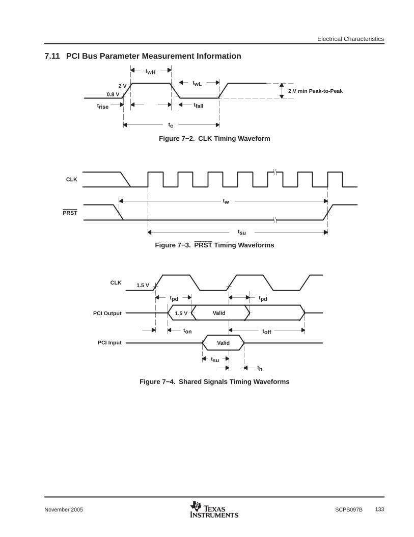
Electrical Characteristics
133November 2005 SCPS097B
7.11 PCI Bus Parameter Measurement Information
twH
2 V
0.8 V
trise tfall
tc
twL2 V min Peak-to-Peak
Figure 7−2. CLK Timing Waveform
tw
tsu
CLK
PRST
Figure 7−3. PRST Timing Waveforms
1.5 V
tpd tpd
Valid1.5 V
ton toff
Valid
tsuth
CLK
PCI Output
PCI Input
Figure 7−4. Shared Signals Timing Waveforms

Glossary
134 November 2005SCPS097B
8 Glossary
ACRONYM DEFINITION
BIST Built-in self test
ECRC End-to-end cyclic redundancy codeEEPROM Electrically erasable programmable read-only memory
GP General purposeGPIO General-purpose input output
ID IdentificationIF InterfaceIO Input outputI2S Inter IC sound
LPM Link power managementLSB Least significant bit
MSB Most significant bitMSI Message signaled interrupts
PCI Peripheral component interface
PME PCI power management event
QoS Quality-of-service
RX Receive
SCL Serial-bus clockSDA Serial-bus data
TC Traffic classTLP Transaction layer packet or protocolTX Transmit
VC Virtual channel
WRR Weighted round-robin

Mechanical Data
135November 2005 SCPS097B
9 Mechanical Data
The XIO2000 device is available in the 201-ball MicroStar BGA package (GZZ) or the 201-ball lead-free (Pbatomic number 82) MicroStar BGA package (ZZZ). The following figures show the mechanical dimensionsfor the packages. The GZZ and ZZZ packages are mechanically identical.

PACKAGING INFORMATION
Orderable Device Status (1) PackageType
PackageDrawing
Pins PackageQty
Eco Plan (2) Lead/Ball Finish MSL Peak Temp (3)
XIO2000GZZ NRND BGA MI CROSTA
R
GZZ 201 TBD Call TI Call TI
XIO2000ZZZ NRND BGA MI CROSTA
R
ZZZ 201 TBD Call TI Call TI
(1) The marketing status values are defined as follows:ACTIVE: Product device recommended for new designs.LIFEBUY: TI has announced that the device will be discontinued, and a lifetime-buy period is in effect.NRND: Not recommended for new designs. Device is in production to support existing customers, but TI does not recommend using this part ina new design.PREVIEW: Device has been announced but is not in production. Samples may or may not be available.OBSOLETE: TI has discontinued the production of the device.
(2) Eco Plan - The planned eco-friendly classification: Pb-Free (RoHS), Pb-Free (RoHS Exempt), or Green (RoHS & no Sb/Br) - please checkhttp://www.ti.com/productcontent for the latest availability information and additional product content details.TBD: The Pb-Free/Green conversion plan has not been defined.Pb-Free (RoHS): TI's terms "Lead-Free" or "Pb-Free" mean semiconductor products that are compatible with the current RoHS requirementsfor all 6 substances, including the requirement that lead not exceed 0.1% by weight in homogeneous materials. Where designed to be solderedat high temperatures, TI Pb-Free products are suitable for use in specified lead-free processes.Pb-Free (RoHS Exempt): This component has a RoHS exemption for either 1) lead-based flip-chip solder bumps used between the die andpackage, or 2) lead-based die adhesive used between the die and leadframe. The component is otherwise considered Pb-Free (RoHScompatible) as defined above.Green (RoHS & no Sb/Br): TI defines "Green" to mean Pb-Free (RoHS compatible), and free of Bromine (Br) and Antimony (Sb) based flameretardants (Br or Sb do not exceed 0.1% by weight in homogeneous material)
(3) MSL, Peak Temp. -- The Moisture Sensitivity Level rating according to the JEDEC industry standard classifications, and peak soldertemperature.
Important Information and Disclaimer:The information provided on this page represents TI's knowledge and belief as of the date that it isprovided. TI bases its knowledge and belief on information provided by third parties, and makes no representation or warranty as to theaccuracy of such information. Efforts are underway to better integrate information from third parties. TI has taken and continues to takereasonable steps to provide representative and accurate information but may not have conducted destructive testing or chemical analysis onincoming materials and chemicals. TI and TI suppliers consider certain information to be proprietary, and thus CAS numbers and other limitedinformation may not be available for release.
In no event shall TI's liability arising out of such information exceed the total purchase price of the TI part(s) at issue in this document sold by TIto Customer on an annual basis.
PACKAGE OPTION ADDENDUM
www.ti.com 21-Apr-2008
Addendum-Page 1