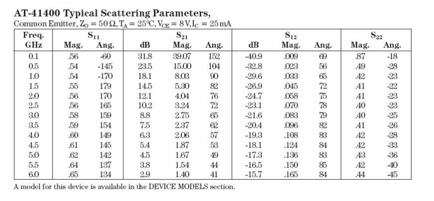
oscillator design example
TRANSCRIPT
Microwave Oscillator Design
Application Note A008
IntroductionThis application note describes a method of designing oscillators usingsmall signal s parameters. The background theory is first developed toproduce the design equations. These equations are then applied to de-velop three different oscillators: a 4 GHz bipolar lumped resonatoroscillator, a 4 GHz bipolar dielectric resonator oscillator, and a 12 GHzGaAs FET dielectric resonator oscillator.
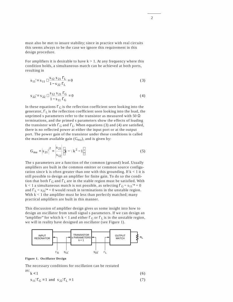
TheoryMicrowave transistors can be used for both amplifier and oscillatorapplications. From the small signal s parameters of the transistor, thestability factor k can be calculated from:
kD s s
s s=
+ − −1
21
211
222
2
21 12
, ( )
where
k s s s s= − ⋅11 22 21 12 2( )
Note that since the transistor s parameters change with frequency, kalso varies with frequency.
A transistor is unconditionally stable at any frequency where k > 1.This condition guarantees that at the specified frequency the transistorwill not oscillate into any termination at either port that has a positiveresistance (i.e. into any impedance that is inside the Smith chart). Tobe mathematically rigorous, we should add that the condition |D| < 1
NOTE: This publication is a reprint of a previously publishedApplication Note and is for technical reference only. For morecurrent information, see the following publications:
• AN1091, 1 and 2 Stage 10.7 to 12.7 GHz Amplifiers Using the
ATF-36163 Low Noise PHEMT, pub. number 5965-1235E.
• AN1136, Low Cost Mixer for the 10.7 to 12.8 GHz Direct
Broadcast Satellite Market, pub. number 5966-2488E.
• AN1139, 950 to 2400 MHz IF Amplifier Using the INA-51063
and INA 54063, pub. number 5966-3363.
2
must also be met to insure stability; since in practice with real circuitsthis seems always to be the case we ignore this requirement in thisdesign procedure.
For amplifiers it is desirable to have k > 1. At any frequency where thiscondition holds, a simultaneous match can be achieved at both ports,resulting in
s ss s
sG
G22 22
12 21
1110 4' ( )= +
−=
ΓΓ
In these equations ΓG is the reflection coefficient seen looking into thegenerator, ΓL is the reflection coefficient seen looking into the load, theunprimed s parameters refer to the transistor as measured with 50 Ωterminations, and the primed s parameters show the effects of loadingthe transistor with ΓG and ΓL. When equations (3) and (4) are satisfied,there is no reflected power at either the input port or at the outputport. The power gain of the transistor under these conditions is calledthe maximum available gain (Gma), and is given by:
G ss
sk kma = = − −
21
2 21
12
2 1 5' ( )
The s parameters are a function of the common (ground) lead. Usuallyamplifiers are built in the common emitter or common source configu-ration since k is often greater than one with this grounding. If k < 1 it isstill possible to design an amplifier for finite gain. To do so the condi-tion that both ΓG and ΓL are in the stable region must be satisfied. Withk < 1 a simultaneous match is not possible, as selecting ΓG = s11'* = 0and ΓL = s22'* = 0 would result in terminations in the unstable region.With k < 1 the amplifier must be less than perfectly matched; manypractical amplifiers are built in this manner.
This discussion of amplifier design gives us some insight into how todesign an oscillator from small signal s parameters. If we can design an“amplifier” for which k < 1 and either ΓG or ΓL is in the unstable region,we will in reality have designed an oscillator (see Figure 1).
Figure 1. Oscillator Design
The necessary conditions for oscillation can be restatedas:
k < 1 6( )
s and sG L11 221 1 7' ' ( )Γ Γ= =
s ss s
sL
L11 11
12 21
2210 3' ( )= +
−=
ΓΓ
INPUTRESONATOR
TRANSISTORs PARAMETERS
k < 1
OUTPUTMATCH RL
ΓG S11' S22' ΓL
3
If the active device selected has a stability factor greater than one atthe desired frequency of oscillation, condition (6) can be achieved ei-ther by changing the two-port configuration (changing from commonemitter to common base or common collector, for example) or by add-ing feedback.
Condition (7) simply confirms that the oscillator produces power atboth ports. If either condition in (7) is satisfied, the other condition isautomatically satisfied. Once we have achieved k < 1, condition (7)gives the necessary relationship to complete the oscillator design. Wewill adopt the technique of resonating the input port and designing amatch that satisfies condition (7) at the output.
The upper frequency for oscillation is limited to fmax, which is the fre-quency where unilateral gain equals unity. The unilateral gain isgenerated by reducing the s parameters to a single gain parametergiven by:
s
s
s
U ss s
k s s s s
11
22
12
212 21 12
21 12 21 12
0
0
0
1 2 18
'
'
'
'/ /
/ Re /( )
===
= =−
− This parameter U is the highest gain the transistor can ever achieve andit is invariant to the common lead. In practice, it is difficult to build auseful oscillator at frequencies above fmax/2.
Design ProcedureOscillator design from s parameters therefore proceeds as follows.First an active device is selected, and its stability factor k is calculatedat the desired frequency of oscillation. If k < 1 the design can proceed.If k > 1, a configuration change must be made or feedback must beadded until k < 1 is achieved.
With k < 1 we know that an input matching circuit having ΓG whichproduces |s22'| > 1 can be found. The design condition is therefore
s22 1 9' ( )>
This condition can be viewed as stating that there is a negative resis-tance at the output port of the terminated transistor. There are manytechniques for realizing such an input circuit, or resonator. Onemethod is to use a computer simulation and optimize for the conditionthat s11 of the one port consisting of the resonator cascaded with thetransistor (this is equal to s22' of the transistor) is greater than unity. Aresonator satisfying the property that |ΓG| = 1 is lossless; this is a desir-able feature in most oscillator designs. Oscillators are often named bythe type of resonator they employ, as shown in Table 1.
4
Table 1.
Resonator Oscillator Name
Cavity High Q or Stable
YIG YTO (YIG Tuned Oscillator)
Varactor VTO (Voltage Tuned Oscillator)
Lossless Transmission Distributed or Microstrip OscillatorLines
Lossless Lumped Lumped OscillatorElement
Dielectric Resonator DRO (Dielectric Resonator Oscillator)
With the input circuit established, the load circuit is designed to satisfy
ΓL s= 1 1022/ ' ( )
which follows directly from condition (7). Note that since |s22'| > 1, thisequation guarantees |ΓL| < 1, i.e. the load resistor will be positive.
For the special case where the oscillator is intended to oscillate di-rectly into a 50 Ω load, no load circuit needs to be designed, and thecondition for oscillation can be re-expressed. If the load is 50 Ω, ΓL = 0.Therefore, since |s22'| ΓL = 1, we have |s22'| = ∞. In practice it hasproven sufficient to design for
s22 100 11' ( )>
Satisfying condition (9) requires |ΓL| < .01, which corresponds to a loadthat is essentially 50 Ω.
The above method will only predict the frequency of oscillation. It pro-vides no information about output power, harmonics, phase noise, orother parameters of possible interest. In general the output power ofthe oscillator will approach the 1 dB compression power (P1 dB) of thetransistor used as an amplifier if the dc bias is designed for maximumP1 dB. Other performance parameters would typically have to be mea-sured from the finished oscillator.
Design ExamplesExample 1: A 4 GHz Lumped Resonator Oscillator
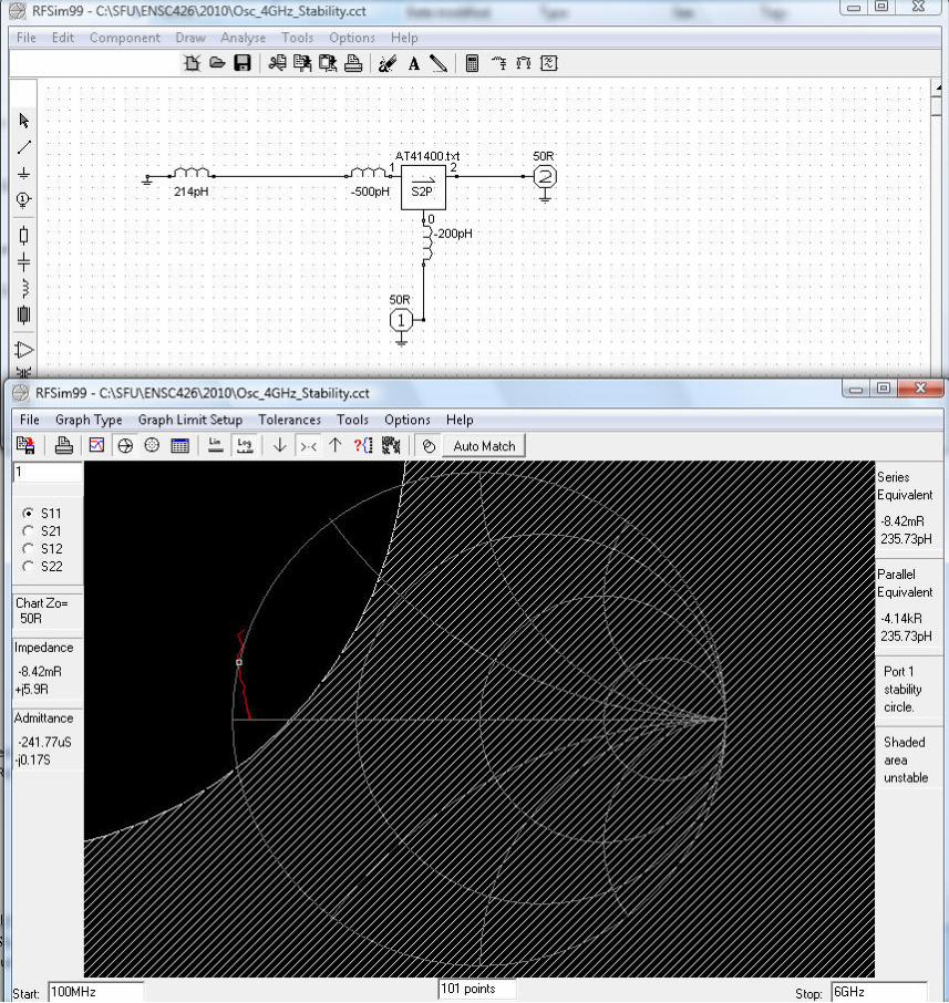
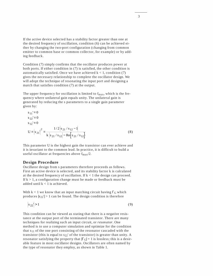
The first example is a computer study of a 4 GHz lumped resonator os-cillator based on the HP AT-41400 bipolar transistor chip. The programused in this design is TOUCHSTONE™ from EEsof; any other linearanalysis and optimization could equally well be used. To achieve an“active device” with k < 1, the transistor chip is used in the commonbase configuration. The catalog common emitter s parameters are usedto describe the transistor chip. The s parameters for a bias of 8 V and25 mA are selected to give the best output power. Since this data in-
5
cludes .5 nH of base bonding inductance and .2 nH of emitter bondinginductance (see reference 1), these parasitics have to be removed (bycascading negative valued inductors) to get to the chip level s param-eters. The .21 nH base bond wire used in the oscillator is included aspart of the “active device” description. Note that the nodal connectionsestablish the emitter as the input and the collector as the output.Analysis shows that this two port has a stability factor k = – .423 at4 GHz. Since this value is less than one, we know that an oscillatordesign is possible.
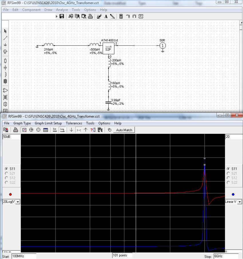
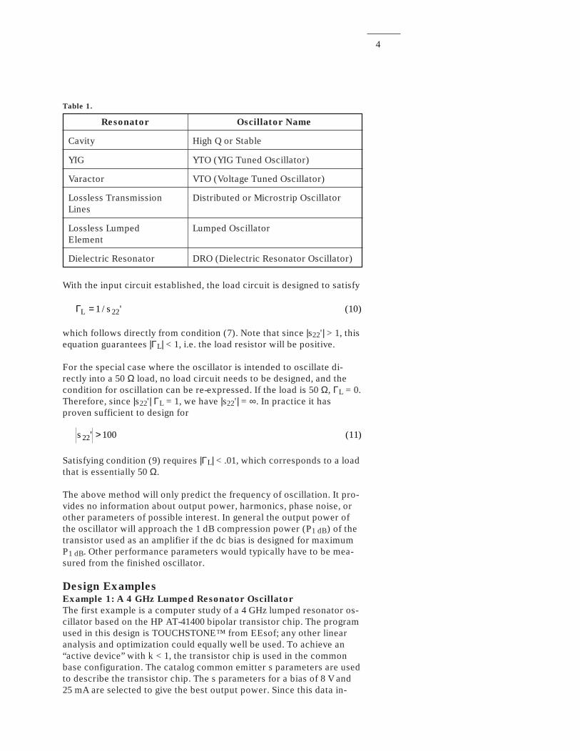
A topology of series inductor (emitter bond wire) – shunt capacitor ischosen for the resonator. Note that other resonator topologies are pos-sible; this choice represents one possible solution that is easily realizedphysically. Initial values are guessed (4 pF for the capacitor, .2 nH forthe inductor) and the circuit is optimized for s11 of the oscillatorgreater than 100. Optimization finds a solution of C = 3.9891 pF; LE =.16044 nH, and LB = .21362 nH. The circuit file is shown in Figure 2,along with the output file. Note MAG[S11] of OSC = 140.756 > 100, i.e.the circuit will oscillate into an essentially 50 Ω load. A schematic forthe finished design is shown in Figure 3.
Figure 2a. Circuit File for 4 GHz Lumped Resonator Oscillator
Figure 2b. Output File for OSCEX1_T
Figure 3. Lumped Resonator
Oscillator at 4 GHz
0.160 nH AT-41400
3.989 pF0.214 nH 50 Ω
s22' = 140.7 ∠ 52.4
VCE = 8 VIC = 25 mA
6
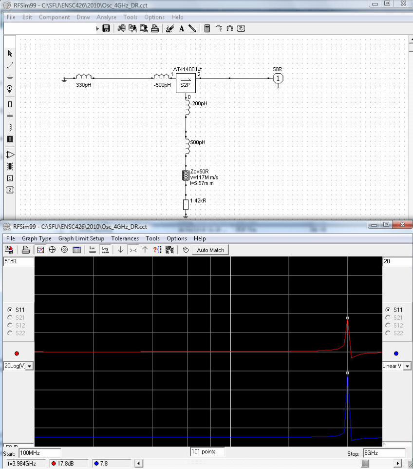
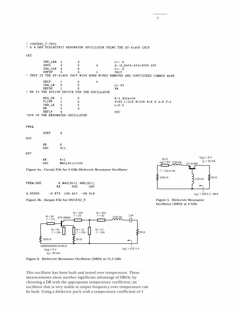
Example 2: A 4 GHz Dielectric Resonator Oscillator
A more interesting circuit to build is an equivalent 4 GHz oscillator thatuses a dielectric resonator (DR) in series configuration to create theinput resonator. In this application the DR is tightly coupled in theTE01δ mode (reference 2) to an input 50 Ω microstripline. This effec-tively creates a very large resistance (i.e. open circuit) at the correctelectrical distance from the transistor, causing oscillation. One advan-tage to using a DR as the input resonator is that the very high unloadedQs of these devices (often on the order of 10000) yields an oscillatorwith little tendency to drift in frequency. The fact that the resonatorconsists effectively of an open circuit that is only coupled to the line atthe frequency of oscillation indicates that at other frequencies the tran-sistor can be terminated in 50 Ω,. greatly reducing the possibility ofsecondary oscillations at undesired frequencies.
Once again the circuit can be simulated and optimized for s11 OSC >100. The dielectric resonator is modeled by a large valued series resis-tor. The initial estimate of 1000 Ω comes from an estimate of 10 for thecoupling coefficient β of the DR to the microstripline (typical for thiskind of application), and the relationship that β = R/(2 Zo). This valueand the distance from the transistor at which the DR is coupled are thevariables for optimization. A printout of the circuit file and the result-ant output are given in Figure 4; the schematic for the resultingoscillator is shown in Figure 5. Measurements on this oscillator (refer-ence 3) show that as predicted the frequency of oscillation is 4 GHz.The observed output power of + 14 dBm is in fair agreement with the+19 dBm level that would be predicted from the P1 dB of the transistor.This oscillator also exhibited excellent phase noise performance,–117 dBc/Hz at 10 KHz from the carrier.
(Phase noise is a way of measuring the “noise skirts” of the oscillator.This noise level is expressed as being a certain level below the oscilla-tion signal, at a certain distance out from the center frequency ofoscillation. High levels of suppression at a narrow spacing indicates avery quiet oscillator.)
Example 3: A 12 GHz Dielectric Resonator Oscillator
Most high performance microwave bipolar transistors have an fmax onthe order of 20 GHz. Thus it is difficult to build oscillators with thesedevices at 12 GHz (above fmax/2). Gallium arsenide field effect transis-tors, with typical fmax values approaching 100 GHz, provide areasonable solution to this problem. Where possible silicon bipolartransistors are used for oscillator design because of their superiorphase noise performance.
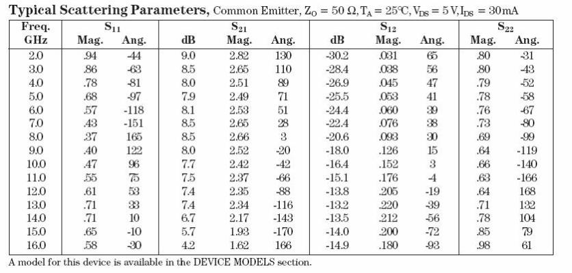
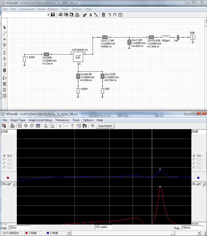
The third example uses a dielectric series resonator to input tune acommon-source GaAs FET, the packaged ATF-26836. The s-parameterdata is taken from the model (reference 4) of the ATF-26836 at a biascondition of 5V, 30 mA. As before a circuit simulation is done, with thevariable for optimization being the position of the DR relative to thetransistor. The resulting circuit is given in Figure 6; this circuit uses adielectric substrate of ε = 2.2 and h = 20 mils.
7
Figure 4a. Circuit File for 4 GHz Dielectric Resonator Oscillator
Figure 4b. Output File for OSCEX2_T Figure 5. Dielectric Resonator
Oscillator (DRO) at 4 GHz
This oscillator has been built and tested over temperature. Thesemeasurements show another significant advantage of DROs: bychoosing a DR with the appropriate temperature coefficient, anoscillator that is very stable in output frequency over temperature canbe built. Using a dielectric puck with a temperature coefficient of 3
Figure 6. Dielectric Resonator Oscillator (DRO) at 11.5 GHz
= 218.8 nils
0.50 nH50 Ω
εeff = 6.6AT-41400
0.33 nH 50 Ω1421 Ω
s22' = 195.4 ∠ –38.9
VCE = 8 VIC = 25 mA
W = 10= 190
W = 10= 250
W = 40= 196
W = 60= 121
W = 339= 26
W = 250= 92 0.50 nH 1 pF
50 Ω
50 Ω1520 Ω
ATF-26836
DIMENSIONS IN MILSs22' = 123 ∠ 4VDS = 5 V
ID = 30 mA
www.hp.com/go/rf
For technical assistance or the location ofyour nearest Hewlett-Packard sales office,distributor or representative call:
Americas/Canada: 1-800-235-0312 or(408) 654-8675
Far East/Australasia: Call your local HPsales office.
Japan: (81 3) 3335-8152
Europe: Call your local HP sales office.
Data Subject to Change
Copyright © 1995 Hewlett-Packard Co.
Obsoletes 5964-3431E
5968-3628E (12/98)
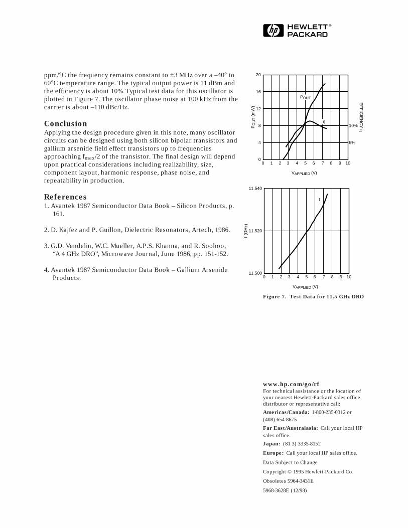
ppm/°C the frequency remains constant to ±3 MHz over a –40° to60°C temperature range. The typical output power is 11 dBm andthe efficiency is about 10%. Typical test data for this oscillator isplotted in Figure 7. The oscillator phase noise at 100 kHz from thecarrier is about –110 dBc/Hz.
ConclusionApplying the design procedure given in this note, many oscillatorcircuits can be designed using both silicon bipolar transistors andgallium arsenide field effect transistors up to frequenciesapproaching fmax/2 of the transistor. The final design will dependupon practical considerations including realizability, size,component layout, harmonic response, phase noise, andrepeatability in production.
References1. Avantek 1987 Semiconductor Data Book – Silicon Products, p.
161.
2. D. Kajfez and P. Guillon, Dielectric Resonators, Artech, 1986.
3. G.D. Vendelin, W.C. Mueller, A.P.S. Khanna, and R. Soohoo,“A 4 GHz DRO”, Microwave Journal, June 1986, pp. 151-152.
4. Avantek 1987 Semiconductor Data Book – Gallium ArsenideProducts.
f (G
Hz)
11.540
108 9764 53210
VAPPLIED (V)
11.520
11.500
f
Figure 7. Test Data for 11.5 GHz DRO
PO
UT (
mW
)
EF
FIC
IEN
CY
η
20
108 9764 53210
VAPPLIED (V)
16
12
8
4
10%
5%
0
POUT
η