organic electronics breakout session report.pdf
TRANSCRIPT
Breakout Report on Organic Electronics
Identification of Grand Challenges
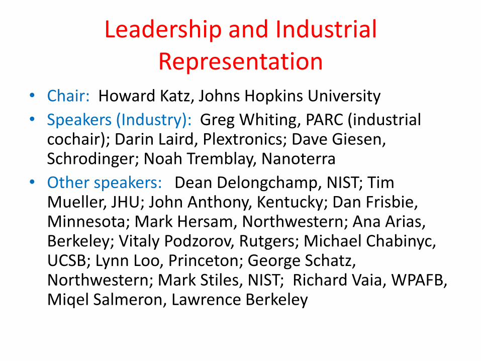
Leadership and Industrial Representation
• Chair: Howard Katz, Johns Hopkins University
• Speakers (Industry): Greg Whiting, PARC (industrial cochair); Darin Laird, Plextronics; Dave Giesen, Schrodinger; Noah Tremblay, Nanoterra
• Other speakers: Dean Delongchamp, NIST; Tim Mueller, JHU; John Anthony, Kentucky; Dan Frisbie, Minnesota; Mark Hersam, Northwestern; Ana Arias, Berkeley; Vitaly Podzorov, Rutgers; Michael Chabinyc, UCSB; Lynn Loo, Princeton; George Schatz, Northwestern; Mark Stiles, NIST; Richard Vaia, WPAFB, Miqel Salmeron, Lawrence Berkeley
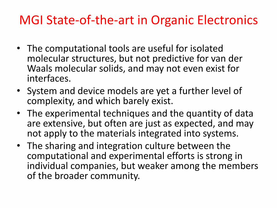
MGI State-of-the-art in Organic Electronics
• The computational tools are useful for isolated molecular structures, but not predictive for van der Waals molecular solids, and may not even exist for interfaces.
• System and device models are yet a further level of complexity, and which barely exist.
• The experimental techniques and the quantity of data are extensive, but often are just as expected, and may not apply to the materials integrated into systems.
• The sharing and integration culture between the computational and experimental efforts is strong in individual companies, but weaker among the members of the broader community.
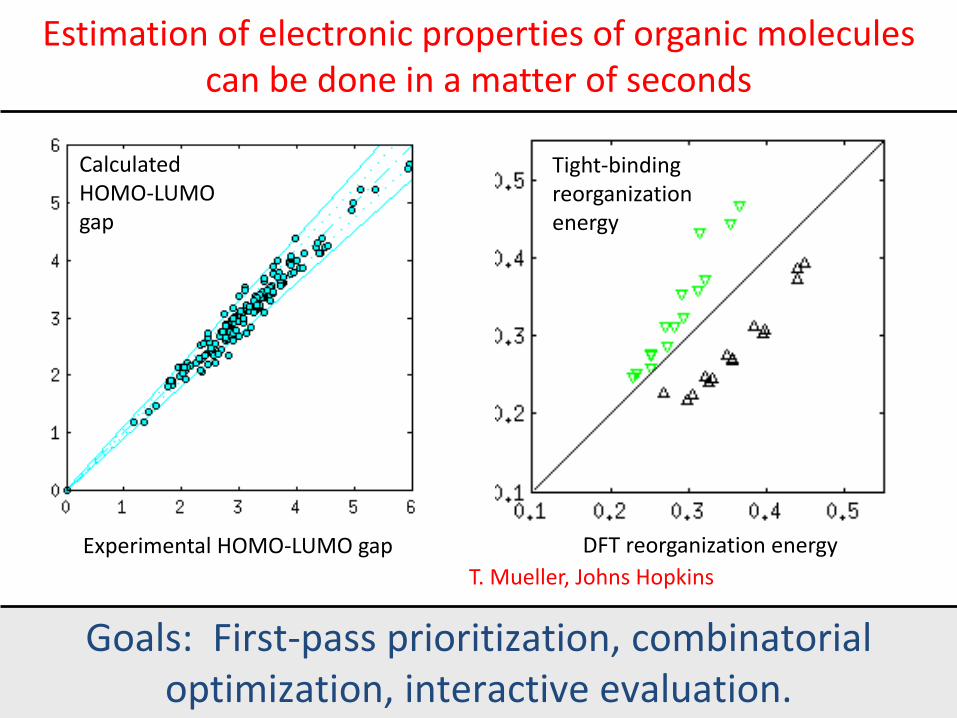
Estimation of electronic properties of organic molecules can be done in a matter of seconds
Experimental HOMO-LUMO gap
Calculated HOMO-LUMO gap
DFT reorganization energy
Tight-binding reorganization energy
Goals: First-pass prioritization, combinatorial optimization, interactive evaluation.
T. Mueller, Johns Hopkins
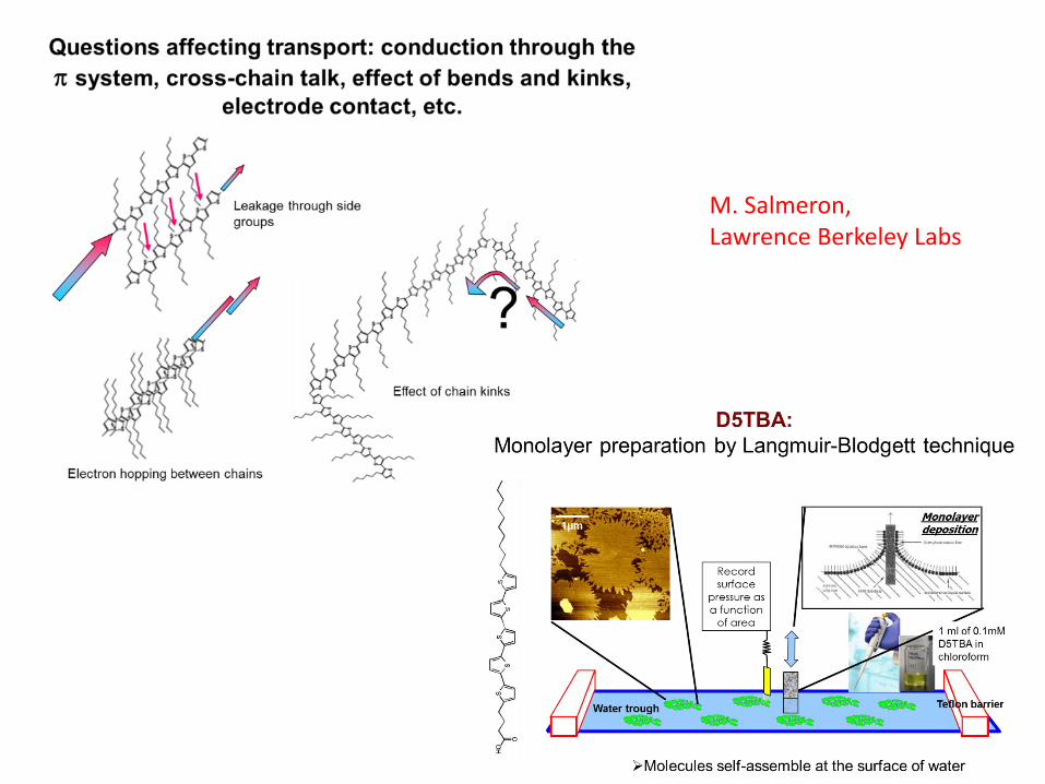
M. Salmeron, Lawrence Berkeley Labs
10-10 10-9 10-8 10-7 10-6 10-5 10-4
molecular
packing
out-of-plane molecular
orientation
in-plane molecular
orientation
L L
lattice
dimensions film thickness
characteristic length scale of ordering, L (meters)
L
device channel length
Homogeneous Organics Show Heterogeneous Alignment
Y.L. Loo, Princeton
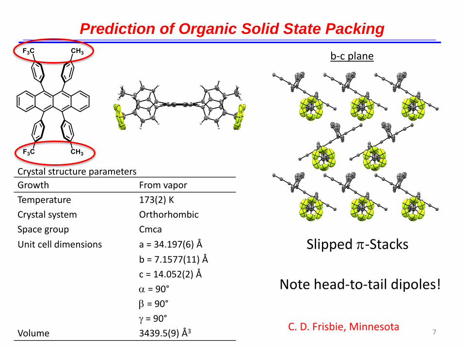
Prediction of Organic Solid State Packing
Slipped p-Stacks
7
Note head-to-tail dipoles!
Crystal structure parameters
Growth From vapor
Temperature 173(2) K
Crystal system Orthorhombic
Space group Cmca
Unit cell dimensions a = 34.197(6) Å
b = 7.1577(11) Å
c = 14.052(2) Å
a = 90°
b = 90°
g = 90°
Volume 3439.5(9) Å3
b-c plane
C. D. Frisbie, Minnesota
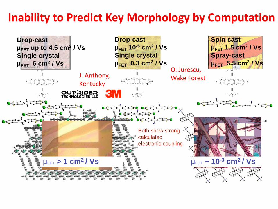
Spin-cast
µFET 1.5 cm2 / Vs
Spray-cast
µFET 5.5 cm2 / Vs
Drop-cast
µFET 10-5 cm2 / Vs
Single crystal
µFET 0.3 cm2 / Vs
Drop-cast
µFET up to 4.5 cm2 / Vs
Single crystal
µFET 6 cm2 / Vs
μFET > 1 cm2 / Vs μFET ~ 10-3 cm2 / Vs
Both show strong
calculated
electronic coupling
J. Anthony, Kentucky
O. Jurescu, Wake Forest
Inability to Predict Key Morphology by Computation
Culture and Landscape • Publication and funding are driven by world record metrics that
might not be the most relevant. Processing and stability/lifetime, and lower performing material explanations, are viewed as less scientific and less fundable, and it is difficult to place the required equipment/computational infrastructure in academic labs. More sustainable collaboration, perhaps through centers, is needed.
• Discontinuous supply chain; multiple inputs to complex systems come from mutually proprietary sources. Communication about issues among companies is lacking, and competition for each part of the supply chain is fierce. Standards are not being generally set.
• Do we need true benchmark performance before modeling can/should be done? Do we have sufficient benchmarks yet? How well can we rely on the results of calculations to make decisions?
• There are no consensus workhorse materials or materials from a single, validated lot. If we chose a workhorse material set now, how would we know when to replace it?
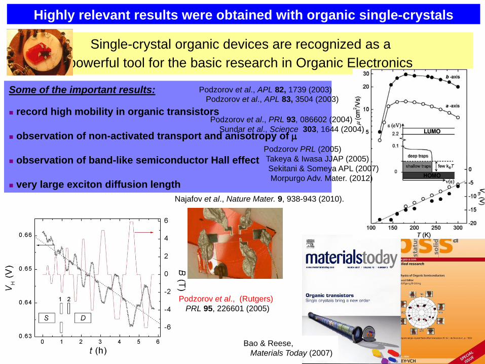
Highly relevant results were obtained with organic single-crystals
devices Single-crystal organic devices are recognized as a
powerful tool for the basic research in Organic Electronics
Some of the important results:
record high mobility in organic transistors
observation of non-activated transport and anisotropy of
observation of band-like semiconductor Hall effect
very large exciton diffusion length
Podzorov et al., (Rutgers)
PRL 95, 226601 (2005)
Bao & Reese,
Materials Today (2007)
Najafov et al., Nature Mater. 9, 938-943 (2010).
Podzorov et al., APL 82, 1739 (2003)
Podzorov et al., APL 83, 3504 (2003)
Podzorov et al., PRL 93, 086602 (2004)
Sundar et al., Science 303, 1644 (2004)
Podzorov PRL (2005)
Takeya & Iwasa JJAP (2005)
Sekitani & Someya APL (2007)
Morpurgo Adv. Mater. (2012)
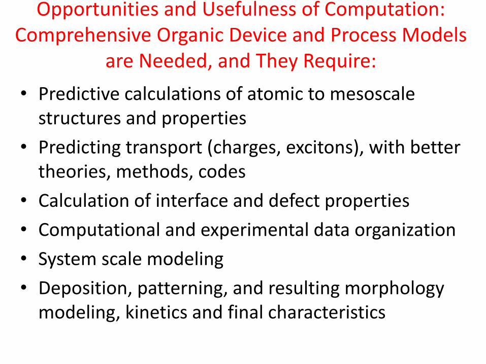
Opportunities and Usefulness of Computation: Comprehensive Organic Device and Process Models
are Needed, and They Require:
• Predictive calculations of atomic to mesoscale structures and properties
• Predicting transport (charges, excitons), with better theories, methods, codes
• Calculation of interface and defect properties
• Computational and experimental data organization
• System scale modeling
• Deposition, patterning, and resulting morphology modeling, kinetics and final characteristics
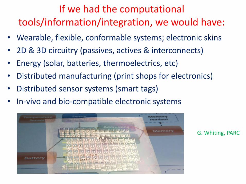
If we had the computational tools/information/integration, we would have:
• Wearable, flexible, conformable systems; electronic skins
• 2D & 3D circuitry (passives, actives & interconnects)
• Energy (solar, batteries, thermoelectrics, etc)
• Distributed manufacturing (print shops for electronics)
• Distributed sensor systems (smart tags)
• In-vivo and bio-compatible electronic systems
G. Whiting, PARC
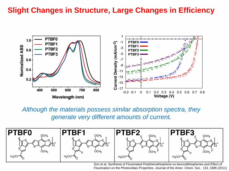
Son et al. Synthesis of Fluorinated Polythienothiophene-co-benzodithiophenes and Effect of
Fluorination on the Photovoltaic Properties. Journal of the Amer. Chem. Soc. 133, 1885 (2011)
Although the materials possess similar absorption spectra, they
generate very different amounts of current.
Slight Changes in Structure, Large Changes in Efficiency
Technical Challenges and Gaps There is an especially glaring deficiency in modeling related to manufacturing steps and processes. Remediating this deficiency will require:
• Tools aimed at the impact of process on formation and evolution of microstructures and electronic properties; flow, solvation, wetting, and annealing process modeling; interfacial interaction modeling; and device modeling
• Infrastructure: integration of computation and experiment
A.C. Arias, UC Berkeley
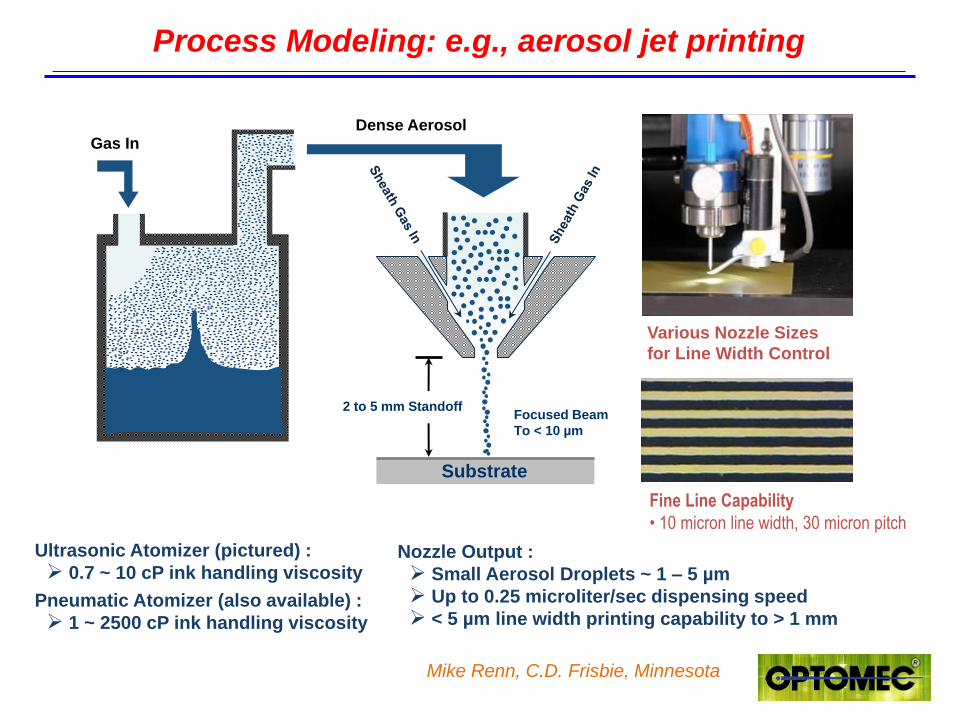
Process Modeling: e.g., aerosol jet printing
Gas In
Focused Beam
To < 10 µm
Dense Aerosol
Substrate
2 to 5 mm Standoff
Various Nozzle Sizes
for Line Width Control
Nozzle Output :
Small Aerosol Droplets ~ 1 – 5 µm
Up to 0.25 microliter/sec dispensing speed
< 5 µm line width printing capability to > 1 mm
Ultrasonic Atomizer (pictured) :
0.7 ~ 10 cP ink handling viscosity
Pneumatic Atomizer (also available) :
1 ~ 2500 cP ink handling viscosity
Fine Line Capability
• 10 micron line width, 30 micron pitch
Mike Renn, C.D. Frisbie, Minnesota
Experiment-Computation Feedback
• Solid state properties: Simple model systems (donor/acceptor interfaces, CNT including effects of chirality, single crystals, uniform heterojunctions). Doping in model systems (ionization efficiency, Fermi level control, thermoelectric effect, electrostatics at interfaces and near defects, chemical and physical sensing)
• Phenomena: Spin, exciton, charge and phonon transport, spin states, Hall mobility, T-dependence of mobility, anisotropy; stability; sensitivity
• Characterization: Advanced structural characterization (XRR, NS), advanced spectroscopy, including absorption and emission, nonlinear, hard and soft x-ray, and time-resolved, scanning probe microscopy, photocurrent spectroscopy
• Massive data: role of machine learning/artificial intelligence, data mining, parameterization
• Data from real devices fed into computation, including reliability and failure analysis
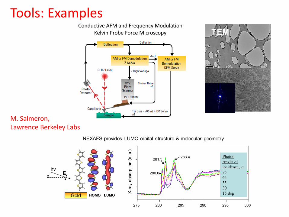
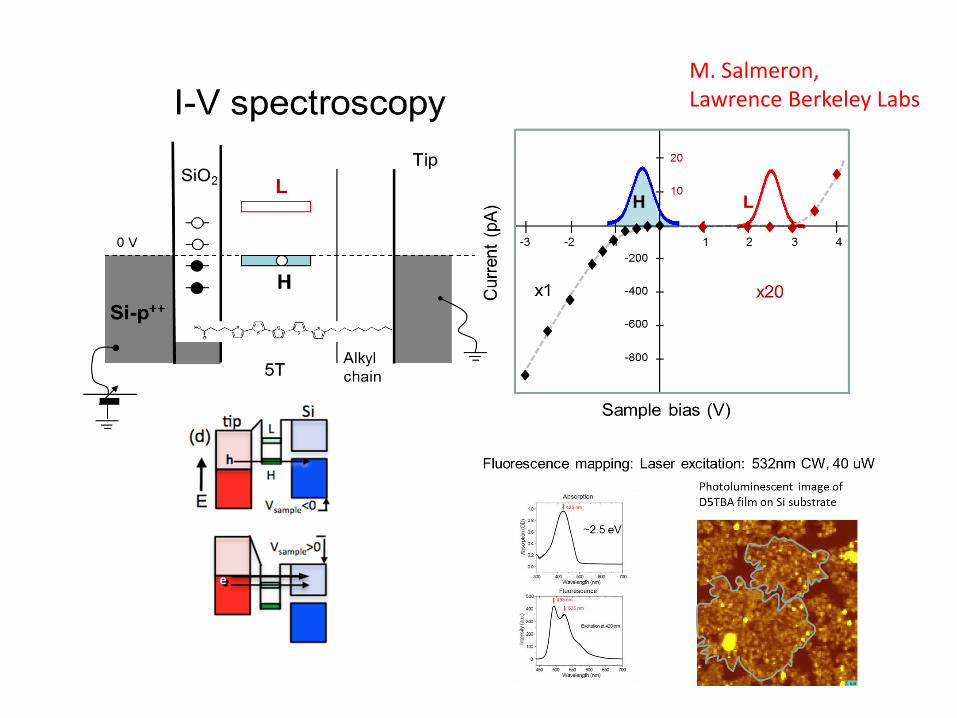
Tools: Examples
M. Salmeron, Lawrence Berkeley Labs
M. Salmeron, Lawrence Berkeley Labs
Inte
nsity*q
2 [
au
]
5 6 7 8
0.012 3 4 5 6 7 8
0.12
q [nm-1
]
Inte
nsity*q
2 [
au
]
5 6 7 8
0.012 3 4 5 6 7 8
0.12
q [nm-1
]
As Cast Pre Annealed Post Annealed Pre & Post
10-2
10-1
100
Sa
t. M
ob
ility
[cm
/Vs]
10008006004002000
Orientational Coherence Length [nm]
Data Fit Confidence
5 6 7 8
0.012 3 4 5 6 7 8
0.12 3
q [nm-2
]
As Cast Pre Annealed Post Annealed Pre and Post
1000 1002p/q [nm]
A
B
1μm
1μm
C
D
Inte
nsi
ty [
au]
E
F
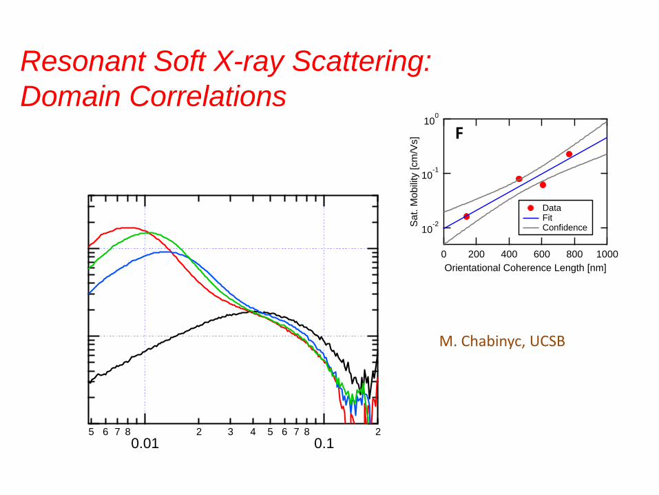
Resonant Soft X-ray Scattering:
Domain Correlations
M. Chabinyc, UCSB
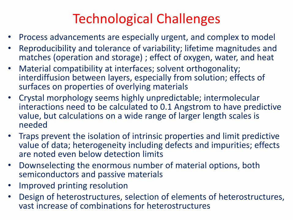
Technological Challenges • Process advancements are especially urgent, and complex to model • Reproducibility and tolerance of variability; lifetime magnitudes and
matches (operation and storage) ; effect of oxygen, water, and heat • Material compatibility at interfaces; solvent orthogonality;
interdiffusion between layers, especially from solution; effects of surfaces on properties of overlying materials
• Crystal morphology seems highly unpredictable; intermolecular interactions need to be calculated to 0.1 Angstrom to have predictive value, but calculations on a wide range of larger length scales is needed
• Traps prevent the isolation of intrinsic properties and limit predictive value of data; heterogeneity including defects and impurities; effects are noted even below detection limits
• Downselecting the enormous number of material options, both semiconductors and passive materials
• Improved printing resolution • Design of heterostructures, selection of elements of heterostructures,
vast increase of combinations for heterostructures
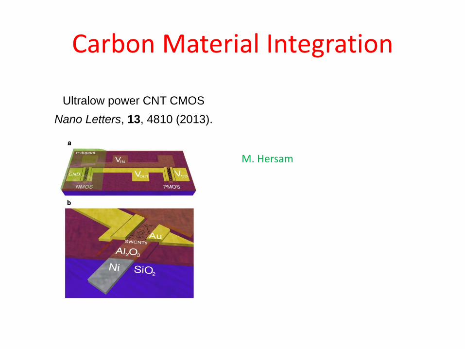
Carbon Material Integration
Ultralow power CNT CMOS
Nano Letters, 13, 4810 (2013).
M. Hersam
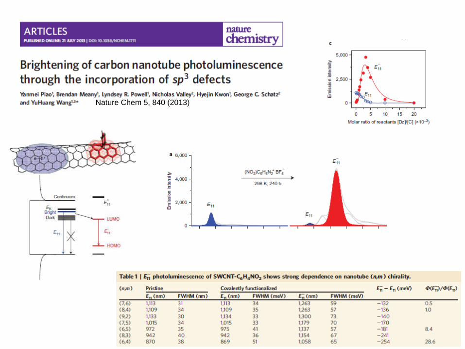
Nature Chem 5, 840 (2013)
Grand Challenge: Prediction of molecular crystal structures
and polymorphs
• Tools are needed for accurate, precise prediction of crystal structures from molecular structure to better predict potential performance from single crystal devices thereby accelerating materials development activities
Grand Challenge: Characterization and modeling at different magnitudes and combinations of length, time and dimensionality scales, including
grain structures and mesoscale crystal/amorphous domain distributions
Molecular modeling alone often not predictive of device properties due to complex structuring in real films. Characterization methods and models to help understand and predict this complex ordering are essential.
Grand Challenge: Creating a liquid-phase manufacturing
paradigm
The big opportunity for this area is that carbon-based materials allow liquid-phase processing techniques (such as printing) to be used for manufacturing of electronics This new manufacturing method requires specific materials, equipment and models that are not currently available in a useful, integrated fashion
Grand Challenge: Projecting device property evolution at the
molecular scale
Performance of organic electronic devices are determined by the materials used and how they are processed. Better understanding of the evolution of molecular-scale structure during processing and it’s impact on device performance is essential
Grand Challenge: Development of a comprehensive model
for organic electronic-biological interfaces
A clear benefit of electronic systems based on soft mater is that they modulus match biological systems well, and so can be used to directly interface with organisms. Developing a model for these interfaces is needed for development of bio-compatible electronic systems
Grand Challenge: Discovering markers for performance
instability
Properties of electronic devices based on organic materials are typically not stable with respect to time, limiting the utility of devices in real systems. Better understanding of the critical markers that determine these instabilities are needed for commercialization of products relying on organic electronic systems
Grand Challenge: Incentivization of industry to reinvest in research
and development (with government partnership)
Greater industrial development is needed In order to accelerate development in this field. A lack of options for significant short-term products and dwindling resources for longer-term research reduces industrial involvement. Methods to incentivize industry to reinvest in this field as the research that will enable the long-term applications is being carried out is necessary.