optical substrate thickness measurement system using hybrid fiber-freespace optics and selective...
TRANSCRIPT
www.elsevier.com/locate/optcom
Optics Communications 269 (2007) 24–29
Optical substrate thickness measurement system using hybridfiber-freespace optics and selective wavelength interferometry
Nabeel A. Riza a,b,*, Mumtaz Sheikh b, Frank Perez a
a Nuonics Inc., 1025 S. Semoran Boulevard, Suite 1093, Winter Park, FL 32792, United Statesb College of Optics/CREOL, University of Central Florida, Box 162700, Orlando, FL 32816, United States
Received 11 May 2006; received in revised form 23 July 2006; accepted 25 July 2006
Abstract
Proposed and demonstrated is a simple few components non-contact thickness measurement system for optical quality semi-transpar-ent samples such as Silicon (Si) and 6H Silicon Carbide (SiC) optical chips used for designing sensors. The instrument exploits a hybridfiber-freespace optical design that enables self-calibrating measurements via the use of confocal imaging via single mode fiber-optics and aself-imaging type optical fiber collimating lens. Data acquisition for fault-tolerant measurements is accomplished via a sufficiently broad-band optical source and a tunable laser and relevant wavelength discriminating optics. Accurate sample thickness processing is achievedusing the known material dispersion data for the sample and the few (e.g., 5) accurately measured optical power null wavelengths producedvia the sample etalon effect. Thicknesses of 281.1 lm and 296 lm are measured for given SiC and Si optical chips, respectively.� 2006 Elsevier B.V. All rights reserved.
1. Introduction
Knowing the exact thickness of optical components is acritical need when designing high quality large, miniature,and super small optics for numerous platforms such as inte-grated-waveguide optics, bulk-optics, and fiber-optics. Overthe years, many methods have been proposed to measurethickness from the thin-film level (i.e., smaller than the opti-cal wavelength) to thick plates (i.e., hundreds of wave-lengths). Perhaps the most tried method is based on theclassic Michelson optical interferometry using a broadbandoptical source such as white light [1,2]. Here, the shortcoherence length of the broadband source is used to pro-duce interferometer arms path-length difference-based out-put detected white light fringes that are processed to obtainthe sample thickness measurement. These white light fringescan be captured in the time domain by scanning a referencemirror over a known scan range and recording the fringe
0030-4018/$ - see front matter � 2006 Elsevier B.V. All rights reserved.
doi:10.1016/j.optcom.2006.07.069
* Corresponding author. Address: College of Optics/CREOL, Univer-sity of Central Florida, Box 162700, Orlando, FL 32816, United States.Tel.: +1 407 823 6829; fax: +1 407 823 6880.
E-mail address: [email protected] (N.A. Riza).
power, with the maximum optically detected power positiongiving data to calculate the sample thickness. This methodhas also been called low coherence reflectometry or timedomain optical coherence tomography (OCT) [3–5]. Analternate twist to white light interferometry is wavelengthscanning interferometry where the broadband source is pro-duced in time by tuning a laser and the interferometer out-put is observed on a per wavelength basis [6–9]. Forinstance, the interferometer output can be dispersed intospatially independent bins representing different wave-lengths along a linear detector array. In this case, by Fouriertransforming the spatially observed optical spectrum, thesample thickness is determined without using any motionof the reference mirror or sample along the optical axis.In a similar fashion by temporally sweeping the laser wave-length and temporally Fourier transforming the fringe data,one can determine the sample optical thickness. These Fou-rier domain approaches are now being referred to as spec-tral domain OCT [10–12]. Even ultra-fast light in theTeraHertz (THz) bandwidth range has been proposed formeasuring optical thickness [13].
As is clear with all the previously mentioned techniquesthat are considered fore-runners in thickness measurement

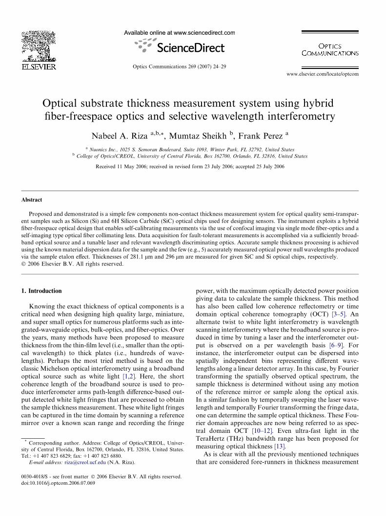
Fig. 1. Proposed thickness measurement system using hybrid freespace-fiber optics and wavelength selective interferometry and processing. BL:broadband light; TL: tunable laser; C: circulator; P: polarizer; PC:polarization controller; OSA: optical spectrum analyzer; SMF: singlemode fiber; 2 · 1/1 · 2: fiber-optic switches.
N.A. Riza et al. / Optics Communications 269 (2007) 24–29 25
instruments, one must use broadband light of the widestoptical spectrum, as shorter the coherence length, the finerthe resolution of the thickness measurement. This in-turnputs an extreme performance requirement on all compo-nents used to assemble the interferometer (e.g., Michelson,Fizeau); in particular, material dispersion effects in theoptical components can become significant, not to mentionincreased non-linear effects arising from non-perfect lineartuning of the laser. In addition, interference fringe powerdata is acquired across the entire optical spectrum toenable the best approximation of the sample thickness.Thus, broader the spectrum to get a better measurementresolution, more data points are needed to obtain thisresolution. Finally and most importantly, a fundamentallimit with these broadband interferometric measurementmethods is that they ignore the test sample material disper-sion effects and hence indeed are only approximations tothe real sample thickness. In fact, the instrument designerfaces a dilemma where a broader spectrum is expected togive the better measurement resolution but at the sametime will add more component and sample material disper-sion effects to the measurement, hence reducing the accu-racy of the measurement.
In this paper, proposed is a possible solution to elimi-nate the effects of using very broadband light, whetherin the interferometer optics or the sample. First, proposedis the use of a direct freespace material dispersion-freelaser beam to interrogate the test sample in air that isexpected to naturally act as the interferometer via theFabry–Perot effect. Thus removed is the need for manymaterial dispersion-free optical components required toassemble for example a Michelson interferometer. Second,proposed is the use of only a few (e.g., five) closely spacedaccurately measured discrete wavelengths, thus removingthe need to acquire optical power data over a very broadcontinuous optical spectrum. Third, sample refractiveindex data at only the chosen few (e.g., five) adjacentwavelengths is needed for processing. Note that todayextensive and accurate material dispersion data in theform of the Sellmeier equation is available for key opticalsubstrate materials such as Silicon (Si) [14] and SiliconCarbide (SiC) [15]. Fourth, the proposed thickness calcula-tion uses a closed-form expression based on Fabry–Perotinterferometry; hence providing an exact measured valuefor the sample thickness. Finally, the use of a single modefiber (SMF) coupled to fiber lens optics insures a confocalself-aligning set-up and hence provides the launching andreception of a high collimation on-axis wireless opticalbeam needed for proper sample access. In effect, the pro-posed system is self-calibrating and insures a true thick-ness measurement. The rest of the letter describes theproposed thickness measurement hybrid fiber-freespacesystem design, implementation, and experimental results.Such a system is ideal for measuring the large thicknessof sample wafers such as Si and 6H-SiC Crystals such asrecently proposed to form wireless optical sensors for tem-perature sensing [16–19].
2. Hybrid fiber-freespace thickness sensor system design
Fig. 1 shows the proposed hybrid fiber-freespace thick-ness sensor system. Because this system relies on the natu-ral Fabry–Perot interferometry produced by the sampleplaced in air (and if needed vacuum), the optical samplemust be a non-scattering partially reflecting (or semi-trans-parent) parallel-plate structure over the optical observationspot. Earlier, a multi-beam interference approach for thick-ness measurements was proposed that was focused onusing broadband light for thin-film (<k) thickness measure-ments for films on thick substrates [20]. This study con-cluded that direct use of all the wideband spectra opticalpower maxima (or minima) and related wavelength valuesis not a very accurate method for measuring the thin-filmthickness. In fact, it was correctly shown that althoughmulti-beam interferometry provides an exact closed-formexpression for the sample thickness, the technique is extre-mely sensitive to the sample material dispersion data andrequires further optical data and processing to produce bet-ter accuracy results [21]. A key reason for this limitationwas the thin-film nature of the sample that caused a large(e.g., 45 nm) separation between adjacent spectra maxima(or minima). This large wavelength separation translatedto a large (e.g., 0.05) refractive index change for the adja-cent wavelength positions for the used amorphous siliconmaterial. In addition, these earlier multi-beam interferom-etry methods provided no instrument self-calibration (orself-alignment) method so the placement of the sampleguaranteed a true thickness reading.
Fig. 1 system solves these problems by using a hybriddesign that uses both fiber and freespace optics and sam-ples such as Si and 6H-SiC whose material dispersion datavia the Sellmeier equations are accurately available in theliterature [14,15]. Furthermore, the typical mentioned Siand 6H-SiC substrates are thick (t� probe wavelength k,e.g. t = 300 lm) leading to small inter-wavelength gaps

26 N.A. Riza et al. / Optics Communications 269 (2007) 24–29
(e.g., <2 nm) that reduces thickness measurement errorsdue to inaccuracies in prior reported wavelength dependentrefractive index data. These sample conditions are indeedmet for the concerned temperature sensor applicationsusing Si and SiC substrates.
Fig. 1 system deploys two optical processing trains.First, a moderate bandwidth (e.g., 10 nm) broadbandsource lights up the sample via control of a 2 · 1 fiber-opti-cal switch. Light from the broadband source passes via theswitch to enter a fiber-optic circulator that directs the lightvia a SMF to a fiber lens. This fiber lens is a special Gradi-ent Index (GRIN) lens that produces an output Gaussianbeam with its minimum beam waist located at a distanced from the output GRIN lens surface. The location ofthe freespace beam waist also marks the location of thesample plane. Note that this minimum beam waist locationis also where the laser beam has near perfect collimation, acondition required for high quality Fabry–Perot interfer-ometry. Hence, plane waves are launched into the parallelfaces of the sample at the localized minimum beam waistspot. To profile the entire substrate, the sample is physi-cally translated in the plane of the beam cross-section.For high accuracy thickness measurements, the laser beammust strike at normal incidence on the sample substrate. Inthe proposed system, this is naturally achieved by aligningthe sample to maximize the received optical power coupledback into the SMF. In other words, only when the sampleacts like a retro-reflecting surface in the minimum beamwaist plane of the incident laser beam does one get the low-est freespace-to-SMF coupling loss [22]. Thus by monitor-ing the received optical power, one can conclude that thesample is correctly aligned for a true thickness measure-ment. Because the sample refractive index and optical lossdue to all system components is known, one can use Fres-nel reflection coefficient theory to estimate the maximumoptical power reflected from a given substrate. Hence,knowing the total expected losses from all components inthe system including the test sample, one can approximatethe expected optical power detected when the sample is cor-rectly aligned. In short, the proposed system provides theself-calibration feature needed for true measurements viaclassic Fabry–Perot interferometry. This maximized lightre-coupled into the SMF passes via the circulator andanother fiber-optic 1 · 2 switch set such that the samplereflected broadband light enters a fiber-coupled opticalspectrum analyzer. The nature of the used broadbandsource is to provide a few observable interference fringesfor the output spectrum. Hence, perhaps 2–5 fringes areneeded to add a 2–5 redundancy into the proposed thick-ness measurement. Hence, unlike previous approaches thatrely on extensive broadband data over continuous and verywide spectra, the proposed sensor only needs spectra dataover a narrow (e.g., 10 nm) range. Specifically, the OSAis used to read the wavelength location of say five fringeminima positions. The accuracy of the wavelength readingdepends on the resolution of the OSA, both in terms ofwavelength and optical power reading. Thus, using the
broadband source and OSA, a first reading of wavelengthpositions is noted. Next, the two optical switches inFig. 1 system are flipped and a tunable laser and opticalpower meter are switched into the measurement systemto take a second reading for wavelength positions. Herethe tuning resolution of the laser combined with the accu-racy of the power meter will determine the accuracy of thetaken wavelength readings. Hence, two sets of wavelengthreadings can be taken to add fault-tolerance to the mea-surement system. Pairs of these adjacent spectral minimareadings in conjunction with the pre-known sample refrac-tive index data via the Sellmeir equations is then used tocompute the sample thickness value at the given probedsample location set by the mechanical translation stage.
It is well known that the optical power reflectance froma Fabry–Perot cavity is given by
RFP ¼R1 þ R2 þ 2
ffiffiffiffiffiffiffiffiffiffi
R1R2
pcos /
1þ R1R2 þ 2ffiffiffiffiffiffiffiffiffiffi
R1R2
pcos /
; ð1Þ
where R1 and R2 are the Fabry–Perot etalon front andback mirror reflectances, respectively. / is the round-trippropagation phase accumulated by an optical beam whilepassing through the sample etalon of thickness t andrefractive index n(k) at a wavelength of k, and is givenby / ¼ 4pnðkÞt
k at normal incidence. For the test substratesample in air, R1 = R2 = R = r2, where r = [n(k) � 1]/[n(k) + 1] is the Fresnel amplitude reflection coefficient ofan air-sample interface. Eq. (1) indicates that the maxi-mum reading of the proposed Fig. 1 system are taken whencos(/) = 1 or / = 2pm, where m = 0,1,2,3, . . ., while theminimum reading of the received optical power are takenwhen cos(/) = �1 or / = (2m � 1)p. Hence, as the wave-length k of the system optical source engaging the samplechanges from one spectrum minimum (or maximum) posi-tion to the adjacent minimum position, the optical path-length in the substrate has changed causing / to changeby 2p radians. Given that the first chosen power minimumoccurs at a measured k1, the sample round-trip propaga-tion phase accumulated is given by: /1 = {4pn(k1)t/k1}.Similarly, for the adjacent power minimum occurring ata measured k2 value, the sample round-trip propagationphase accumulated is given by: /2 = {4pn(k2)t/k2}. Giventhat for any two chosen adjacent spectra power minimawith k2 > k1 the round-trip optical phase changes by 2p,/1 � /2 can be written to give the sample closed-form ex-act optical thickness value t of
t ¼ k1k2
2ðk2n1 � k1n2Þ; ð2Þ
where n(k1) = n1 and n(k2) = n2.
3. Experimental demonstration
Fig. 1 system is set up in the laboratory. The broadbandsource is an edge-emitting light emitting diode (EE-LED)that acts as an internal source for the Agilent Model86142B OSA with a direct wavelength detection resolution

N.A. Riza et al. / Optics Communications 269 (2007) 24–29 27
of 0.06 nm and an interpolated wavelength reading resolu-tion of 0.001 nm. The tunable laser is a Santec ModelTSL210 with a tuning resolution of 0.01 nm. The self-colli-mating fiber Graded Index (GRIN) lens from LightPathTechnologies has a half self-imaging distance d of12.5 cm. The GRIN lens forms its 1/e2 minimum beamwaist diameter of 1 mm on the sample plane. The test sub-strate Si or SiC sample sits on a precision x–y–z Newportmechanical translation stage. A mechanical control Polari-zation Controller (PC) is used for maximizing the power inthe freespace launched p-polarization of the beam. Theoptical circulator has a 1.7 dB optical loss. A NewportPower Meter Model 1830C and related detector Model883IR are used for precision power measurements. Byadjusting a test mirror of the x–y–z stage, the maximumfreespace to single mode fiber (SMF) coupling is achievedindicating a source SMF-in to detection SMF-out totaloptical loss of 3.2 dB. This loss includes SMF connectors,PC, circulator, freespace-SMF coupling, and polarizerlosses. Next, the SiC and Si samples are mounted on thex–y–z stage and mechanically optimized with a tilt resolu-tion of <0.01� to insure the equivalent low coupling losslevels indicating true normal incidence strike of the laserbeam on the samples [22]. Mechanically switched fiber con-nectors are used instead of electronically controlled 1 · 2and 2 · 1 optical switches to complete the data gathering.First, the OSA is used to optimize and observe the samplereflected spectrum minima wavelengths. Then the tunablelaser and power meter are used to confirm these wavelengthreadings and optimize them if needed.
Fig. 2. OSA output for SiC sample showing the five selected wavelengths aspectrum.
Figs. 2 and 3 show the selected power minima five wave-lengths for the 6H-SiC and Si substrates, respectively. Inboth cases, the substrate cuts are such that the materialhas one refractive index in the plane containing the linearpolarization and these refractive indices are given by thefollowing Sellmeier equations:
For 6H : SiCðordinary indexÞ; n2ðkÞ ¼ Aþ Bk2
k2 � C; ð3Þ
where A = 1, B = 5.5515, C = 0.026406, and k is in lm[15]. In particular, the crystal or c-axis for the given 6H-SiC chip is along the optical beam propagation directionand the crystal ordinary index is given to be normal tothe crystal c-axis. Hence the incident linear polarizationsees the given ordinary index in Eq. (3) for the 6H-SiC chip
For Si; n2ðkÞ ¼ eþ A
k2þ Bk2
1
k2 � k21
; ð4Þ
where k1 = 1.1071 lm, e = 11.6858, A = 0.939816, B =0.00810461, and k is in lm [14].
Table 1 shows the five measured pairs of wavelengthsused for thickness processing using the relevant Sellmeierequations in Eqs. (3) and (4). The wavelengths readingsvia the OSA have a 0.001 nm resolution. Table 1 showsthe calculated refractive index values listed to the sixth dec-imal place as consistent with the general accuracy of theused Sellmeier coefficients. Using Table 1 data, the aver-aged experimentally measured thickness value for the SiCsample is 281.1 lm with a ±0.53 lm standard deviation.Similarly, the averaged experimentally measured thickness
t the five consecutive optical power minima positions in the continuous

Fig. 3. OSA output for Si sample showing the five selected wavelengths at the five consecutive optical power minima positions in the continuous spectrum.
Table 1Experimental results for the calculated thickness for SiC and Si
k1 (nm) k2 (nm) n1 n2 t (lm)
SiC 1551.806 1550.162 2.571585 2.571611 281.81550.162 1548.517 2.571611 2.571637 281.11548.517 1546.872 2.571637 2.571662 280.51546.872 1545.234 2.571662 2.571688 281.1
Si 1549.539 1548.411 3.476221 3.476306 296.01548.411 1547.285 3.476306 3.476391 296.11547.285 1546.160 3.476391 3.476476 295.91546.160 1545.038 3.476476 3.476561 296.2
28 N.A. Riza et al. / Optics Communications 269 (2007) 24–29
value for the Si sample is 296.05 lm with a ±0.13 lm stan-dard deviation. For comparison, an alternate commercialthickness measurement mechanical gauge from MitutoyoJapan model 293-330 with a measurement accuracy witha digital readout to the nearest 1 lm (or ±0.5 lm) is usedto measure the Si and SiC sample thicknesses. Using thisphysical contact-based method, the thicknesses for Si andSiC samples are measured to be 296 lm and 281 lm,respectively. These comparative results are in excellentagreement with the optically measured thicknesses usingthe proposed hybrid system deploying wavelength selectiveinterferometry. Specifically, for the SiC case, both tech-niques have a near ±0.5 lm measurement standard devia-tion. Note that for the Si case, the optical measurementhas �4 times better measurement accuracy.
There are several factors that control the thickness mea-surement accuracy from the proposed Fig. 1 system. Ide-ally, one assumes a laser with a fixed wavelength andoptical power level when the OSA records the spectrum
minima locations. In reality, the laser has noise in its fre-quency/time and power content and these random pro-cesses limit the accuracy of the thickness measurementdue to spectrum peak/null shifts. Furthermore, thedeployed OSA instrument has its own wavelength andpower measurement resolution that must be high enoughto operate the OSA above the light source noise levels. Inthe experiment described, the OSA had a 0.001 nm interpo-lated wavelength resolution and a 0.01 dB m (i.e., 10 lW)optical power measurement resolution. The wavefrontquality of the light region striking the optical chip is alsoan important parameter that effects thickness measurementaccuracy. Specifically, the wavefront should ideally be flatto produce high quality deep interference nulls that canbe clearly deciphered by the OSA. In effect, the chip undertest should also have flat faces to maintain the high flatness(e.g., k/50) of the retro-reflecting interfering wavefronts.Finally, as also seen from Eqs. (2)–(4), the improved accu-racy of the deployed Sellmeier coefficients translates intoimproved accuracy of the computed thickness measure-ment. As the proposed instrument uses multiple spectralminima (or maxima) readings to compute the measuredchip thickness, one implements a data averaging operationconsistent when dealing with optical phenomena exhibitingfundamental random noise processes within the time/fre-quency/space context.
Also do note that improved localized thickness measure-ments are possible using a smaller probe beam such as froma 0.29 pitch imaging type fiber GRIN lens (see Fig. 4). Thisapproach is appropriate for small sample thicknesses, i.e.,the sample thickness is smaller than the Rayleigh distance
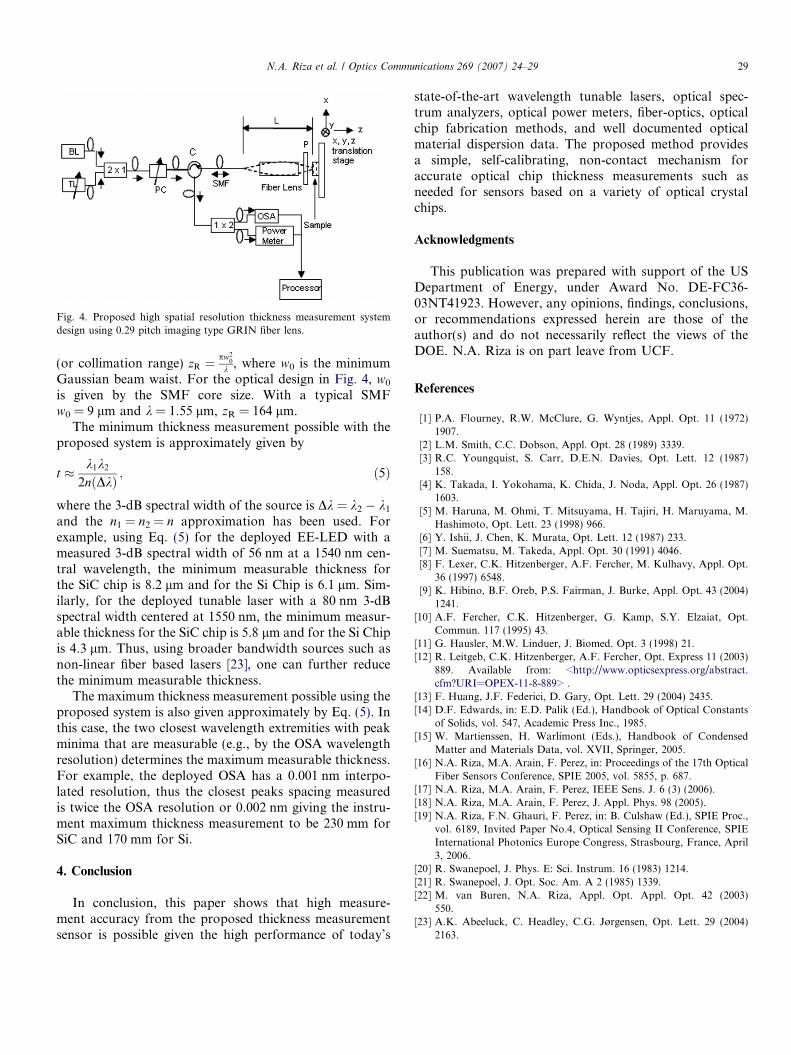
Fig. 4. Proposed high spatial resolution thickness measurement systemdesign using 0.29 pitch imaging type GRIN fiber lens.
N.A. Riza et al. / Optics Communications 269 (2007) 24–29 29
(or collimation range) zR ¼pw2
0
k , where w0 is the minimumGaussian beam waist. For the optical design in Fig. 4, w0
is given by the SMF core size. With a typical SMFw0 = 9 lm and k = 1.55 lm, zR = 164 lm.
The minimum thickness measurement possible with theproposed system is approximately given by
t � k1k2
2nðDkÞ ; ð5Þ
where the 3-dB spectral width of the source is Dk = k2 � k1
and the n1 = n2 = n approximation has been used. Forexample, using Eq. (5) for the deployed EE-LED with ameasured 3-dB spectral width of 56 nm at a 1540 nm cen-tral wavelength, the minimum measurable thickness forthe SiC chip is 8.2 lm and for the Si Chip is 6.1 lm. Sim-ilarly, for the deployed tunable laser with a 80 nm 3-dBspectral width centered at 1550 nm, the minimum measur-able thickness for the SiC chip is 5.8 lm and for the Si Chipis 4.3 lm. Thus, using broader bandwidth sources such asnon-linear fiber based lasers [23], one can further reducethe minimum measurable thickness.
The maximum thickness measurement possible using theproposed system is also given approximately by Eq. (5). Inthis case, the two closest wavelength extremities with peakminima that are measurable (e.g., by the OSA wavelengthresolution) determines the maximum measurable thickness.For example, the deployed OSA has a 0.001 nm interpo-lated resolution, thus the closest peaks spacing measuredis twice the OSA resolution or 0.002 nm giving the instru-ment maximum thickness measurement to be 230 mm forSiC and 170 mm for Si.
4. Conclusion
In conclusion, this paper shows that high measure-ment accuracy from the proposed thickness measurementsensor is possible given the high performance of today’s
state-of-the-art wavelength tunable lasers, optical spec-trum analyzers, optical power meters, fiber-optics, opticalchip fabrication methods, and well documented opticalmaterial dispersion data. The proposed method providesa simple, self-calibrating, non-contact mechanism foraccurate optical chip thickness measurements such asneeded for sensors based on a variety of optical crystalchips.
Acknowledgments
This publication was prepared with support of the USDepartment of Energy, under Award No. DE-FC36-03NT41923. However, any opinions, findings, conclusions,or recommendations expressed herein are those of theauthor(s) and do not necessarily reflect the views of theDOE. N.A. Riza is on part leave from UCF.
References
[1] P.A. Flourney, R.W. McClure, G. Wyntjes, Appl. Opt. 11 (1972)1907.
[2] L.M. Smith, C.C. Dobson, Appl. Opt. 28 (1989) 3339.[3] R.C. Youngquist, S. Carr, D.E.N. Davies, Opt. Lett. 12 (1987)
158.[4] K. Takada, I. Yokohama, K. Chida, J. Noda, Appl. Opt. 26 (1987)
1603.[5] M. Haruna, M. Ohmi, T. Mitsuyama, H. Tajiri, H. Maruyama, M.
Hashimoto, Opt. Lett. 23 (1998) 966.[6] Y. Ishii, J. Chen, K. Murata, Opt. Lett. 12 (1987) 233.[7] M. Suematsu, M. Takeda, Appl. Opt. 30 (1991) 4046.[8] F. Lexer, C.K. Hitzenberger, A.F. Fercher, M. Kulhavy, Appl. Opt.
36 (1997) 6548.[9] K. Hibino, B.F. Oreb, P.S. Fairman, J. Burke, Appl. Opt. 43 (2004)
1241.[10] A.F. Fercher, C.K. Hitzenberger, G. Kamp, S.Y. Elzaiat, Opt.
Commun. 117 (1995) 43.[11] G. Hausler, M.W. Linduer, J. Biomed. Opt. 3 (1998) 21.[12] R. Leitgeb, C.K. Hitzenberger, A.F. Fercher, Opt. Express 11 (2003)
889. Available from: <http://www.opticsexpress.org/abstract.cfm?URI=OPEX-11-8-889> .
[13] F. Huang, J.F. Federici, D. Gary, Opt. Lett. 29 (2004) 2435.[14] D.F. Edwards, in: E.D. Palik (Ed.), Handbook of Optical Constants
of Solids, vol. 547, Academic Press Inc., 1985.[15] W. Martienssen, H. Warlimont (Eds.), Handbook of Condensed
Matter and Materials Data, vol. XVII, Springer, 2005.[16] N.A. Riza, M.A. Arain, F. Perez, in: Proceedings of the 17th Optical
Fiber Sensors Conference, SPIE 2005, vol. 5855, p. 687.[17] N.A. Riza, M.A. Arain, F. Perez, IEEE Sens. J. 6 (3) (2006).[18] N.A. Riza, M.A. Arain, F. Perez, J. Appl. Phys. 98 (2005).[19] N.A. Riza, F.N. Ghauri, F. Perez, in: B. Culshaw (Ed.), SPIE Proc.,
vol. 6189, Invited Paper No.4, Optical Sensing II Conference, SPIEInternational Photonics Europe Congress, Strasbourg, France, April3, 2006.
[20] R. Swanepoel, J. Phys. E: Sci. Instrum. 16 (1983) 1214.[21] R. Swanepoel, J. Opt. Soc. Am. A 2 (1985) 1339.[22] M. van Buren, N.A. Riza, Appl. Opt. Appl. Opt. 42 (2003)
550.[23] A.K. Abeeluck, C. Headley, C.G. Jørgensen, Opt. Lett. 29 (2004)
2163.