on the nucleation of pdsi and nisi2 during the ternary ni ... fileon the nucleation of pdsi and...
TRANSCRIPT

On the nucleation of PdSi and NiSi2 during the ternary Ni(Pd)/Si(100) reactionA. Schrauwen, J. Demeulemeester, A. Kumar, W. Vandervorst, C. M. Comrie, C. Detavernier, K. Temst, and A.
Vantomme Citation: Journal of Applied Physics 114, 063518 (2013); doi: 10.1063/1.4818333 View online: http://dx.doi.org/10.1063/1.4818333 View Table of Contents: http://scitation.aip.org/content/aip/journal/jap/114/6?ver=pdfcov Published by the AIP Publishing
[This article is copyrighted as indicated in the article. Reuse of AIP content is subject to the terms at: http://scitation.aip.org/termsconditions. Downloaded to ] IP:
160.103.2.236 On: Tue, 21 Jan 2014 15:53:01

On the nucleation of PdSi and NiSi2 during the ternary Ni(Pd)/Si(100) reaction
A. Schrauwen,1,a) J. Demeulemeester,1 A. Kumar,2,1 W. Vandervorst,2,1 C. M. Comrie,3,4
C. Detavernier,5 K. Temst,1 and A. Vantomme1
1Instituut voor Kern- en Stralingsfysica, KU Leuven, Celestijnenlaan 200 D, B-3001 Leuven, Belgium2Imec, Kapeldreef, B-3001 Leuven, Belgium3Department of Physics, University of Cape Town, Rondebosch 7700, South Africa4Materials Research Department, iThemba LABS, P.O. Box, Somerset West 7129, South Africa5Department of Solid State Sciences, Ghent University, 9000 Gent, Belgium
(Received 18 June 2013; accepted 29 July 2013; published online 13 August 2013)
During the solid phase reaction of a Ni(Pd) alloy with Si(100), phase separation of binary Ni- and
Pd-silicides occurs. The PdSi monosilicide nucleates at temperatures significantly below the widely
accepted nucleation temperature of the binary system. The decrease in nucleation temperature
originates from the presence of the isomorphous NiSi, lowering the interface energy for PdSi
nucleation. Despite the mutual solubility of NiSi and PdSi, the two binaries coexist in a temperature
window of 100 �C. Only above 700 �C a Ni1–xPdxSi solid solution is formed, which in turn postpones
the NiSi2 formation to a higher temperature due to entropy of mixing. Our findings highlight the overall
importance of the interface energy for nucleation in ternary systems. VC 2013 AIP Publishing LLC.
[http://dx.doi.org/10.1063/1.4818333]
I. INTRODUCTION
Metal silicides, i.e., compounds between metal and sili-
con, have been subjected to scrutiny over the last four deca-
des due to their beneficial properties as electrodes in
semiconductor devices.1 Silicides are typically formed by a
thermal reaction of a metallic thin film with Si, in which
crystalline silicide phases form sequentially. Nucleation of-
ten plays an important role in the formation of a next phase,
especially when the free energy gain DG for the phase transi-
tion is small. In this case, the nucleation barrier, which is a
measure for the energy needed to nucleate and grow a phase,
increases and it is likely that phase formation does not pro-
ceed for insufficient temperatures.2 A well-known example
of a nucleation controlled reaction is the formation of NiSi2from NiSi and Si. The NiSi monosilicide phase is currently
implemented as electrical contact material in transistor devi-
ces, and nucleation of the highly resistive NiSi2 is detrimen-
tal for the purpose of contact formation due to its high
resistivity and its non-uniform interface.3 To increase the
NiSi processing window, research has been dedicated to
postpone the NiSi2 nucleation, which in fact comes down to
controlling the nucleation barrier of NiSi2. This can, for
instance, be achieved by alloying the Ni thin film. The effect
of alloying elements can be qualitatively understood in terms
of the classical nucleation theory in which a nucleation bar-
rier DG� is introduced
DG� � Dr3
ðDH � TDSÞ2; (1)
with T the temperature, Dr the difference in interfacial
energy, DH the enthalpy change of the transition, and DS the
entropy change. The energy needed for the creation of a new
interface between the nucleating phase and the original matrix
depends on the lattice match and interface structure. For exam-
ple, the transition temperature of GdSi1.7!GdSi2 is related to
the crystalline quality of the hexagonal GdSi1.7, which can be
strongly improved by forming the silicide epitaxially, through
channeled ion beam synthesis.4 Alloying elements will alter
Dr by altering the texture or offering low energy interfaces.
Conversely, because DH is typically small for nucleation con-
trolled reactions, alloying elements significantly increase the
importance of DS, especially when isomorphous phases exist
which exhibit mutual solid solubility. Based on the entropy of
mixing two cases can be distinguished that will either decrease
or increase the nucleation barrier, namely for a phase transition
from a mixed phase to a non-mixed phase or vice versa. An
example of both cases, focussing on the nucleation controlled
transition NiSi!NiSi2, is the enhanced formation of the disi-
licide Co1–xNixSi2 from a CoSi/NiSi mixture and the delayed
nucleation of NiSi2 from a Ni1–xPtxSi solid solution.5–7 The
presence of the isomorphous phases NiSi2 and CoSi2 on the
one hand and NiSi and PtSi on the other hand is crucial to
allow solid solubility and, consequently, to affect the sign of
DS. As NiSi and PtSi, PdSi also shares the same crystal struc-
ture and alloying Ni with Pd has been shown to delay NiSi2nucleation.8,9 The effect is generally explained similar to Pt by
stating that a Ni1–xPdxSi solid solution forms.8,10–14 On the
other hand, significant differences between the Pt-Si and Pd-Si
solid phase reaction imply that the formation of a Ni1–xPdxSi
solid solution cannot be simply assumed. Although the
binary reaction sequences for both elements are similar, i.e.,
M!M2Si!MSi (with M¼ Pt or Pd), the very small DH for
the reaction Pd2Si! PdSi, makes PdSi a high temperature
nucleation controlled phase, in contrast to the diffusion con-
trolled formation of PtSi at much lower temperatures: on
Si(100) substrates PdSi only nucleates above 735 �C and on
Si(111) only above 850 �C, while PtSi can form at tempera-
tures as low as 350 �C.2 Furthermore, annealing below thea)[email protected]
0021-8979/2013/114(6)/063518/5/$30.00 VC 2013 AIP Publishing LLC114, 063518-1
JOURNAL OF APPLIED PHYSICS 114, 063518 (2013)
[This article is copyrighted as indicated in the article. Reuse of AIP content is subject to the terms at: http://scitation.aip.org/termsconditions. Downloaded to ] IP:
160.103.2.236 On: Tue, 21 Jan 2014 15:53:01

eutectic temperature, drives PdSi back to Pd2Si.15,16 In order
for a NiSi-PdSi mixture or Ni1–xPdxSi solid solution to form,
assumed to delay NiSi2 formation, PdSi should thus nucleate
at a temperature below the NiSi degradation temperature to
NiSi2. As the latter already occurs around a temperature of
800 �C in the pure Ni-Si system, together with the high nuclea-
tion temperature of PdSi, the entropy of mixing cannot
be automatically assumed as an explanation and the mecha-
nism for NiSi2 postponement by adding Pd is thus unclear at
present.
In most cases, the reaction of a ternary system is by far
more complex than that of the binary constituents. In this pa-
per, we will focus on how the isomorphous phases NiSi and
PdSi influence the nucleation controlled growth of PdSi and
NiSi2, respectively. The understanding of these results will
lead to new insights in the reaction mechanisms and impor-
tant parameters for ternary reactions in general. To this end
the crystalline phase formation and Pd redistribution during
the reaction is studied in situ using real-time X-ray diffrac-
tion (XRD) and real-time Rutherford backscattering spec-
trometry (RBS) and ex situ with atom probe tomography
(APT).
II. EXPERIMENTAL DETAILS
A set of 45 nm Ni(Pd) alloy thin films containing
increasing amounts of Pd (0%, 5%, 10%, and 15% Pd) were
prepared. All metallic films were sputter deposited on
Si(100) substrates, which had previously been cleaned by the
standard RCA procedure and subsequent HF-dip. The crys-
talline phase formation sequence was studied using in situXRD. Every 2 s, a linear detector covering 20� in 2h records
the diffracted x-rays originating from a Cu Ka source, while
ramp annealing the sample at 1 �C/s to 910 �C. Such in situXRD measurements are conventionally displayed as contour
plots of the diffracted intensity as a function of diffraction
angle (y-axis) and temperature (x-axis), see Fig. 1. The
appearance and subsequent disappearance of sets of diffrac-
tion peaks represents the transformation of crystalline phases
as a function of temperature, in a single run. For clarity, the
crystalline phases that could be identified are indicated in the
figure at their corresponding diffraction peaks.
To complement the information on crystalline phase for-
mation extracted from in situ XRD with elemental depth in-
formation, two techniques have been used: (i) RBS and (ii)
APT. RBS is a well-established ion beam technique in thin
film research, which is fully quantitative in elemental com-
position and depth. In this study, RBS is applied in situ, i.e.,
during the thermal treatment.17 This approach provides the
concentration depth profile of all elements as a function of
temperature. In addition, to obtain lateral information on the
Pd distribution, including Pd grain boundary decoration and
Pd clustering, quenches were made at important stages dur-
ing the growth and were investigated with APT. In an APT
experiment, a tip is fabricated from the silicide film, using
focussed ion beam milling. Atom per atom is then released
from the apex of the tip by the application of regular laser
pulses providing the energy needed for evaporation and ioni-
zation. The applied electric field between the tip and the 2D
position sensitive detector (PSD) guides the ions to the PSD.
Together with the laser pulse frequency, a 3D quantitative
elemental map of the tip can be reconstructed with atomic
resolution.18
III. RESULTS AND DISCUSSION
Figure 1(a) displays the in situ XRD measurement for
the reaction of a 45 nm pure Ni film with Si(100), which
serves as a reference to disentangle the effect of Pd addition.
The reaction sequence proceeds as follows:
Ni! d-Ni2Siþ h-Ni2Si ðtransient growthÞ! NiSi! NiSi2: (2)
During the reaction between 200 �C and 450 �C, generally
referred to as the metal rich phase formation, first the
d-Ni2Si forms after which the metastable non-stoichiometric
h phase transiently grows through texture inheritance from
the preceding d-Ni2Si fiber.19 NiSi subsequently grows at the
expense of d-Ni2Si around 320 �C and degrades at about
820 �C. This corresponds to NiSi2 formation, but NiSi2escapes detection due to its expected epitaxial growth on
Si(100). These observed results correspond to what is known
from literature.20 Adding Pd changes the reaction sequence
significantly, as can be inferred from Figs. 1(b)–1(d) show-
ing the in situ XRD measurements on 45 nm Ni(Pd) films
containing 5%, 10%, and 15% of Pd, respectively. The reac-
tion sequence in all three cases generally proceeds as
Ni ���!350�C
d-Ni2Si ���!400�CNiSi ���!
500�CNiSiþ Pd2Si
���!600�CNiSiþ PdSi ���!700�C
Ni1�xPdxSi; (3)
FIG. 1. In situ XRD measurements collected from 45 nm Ni(Pd) alloys con-
taining increasing amounts of Pd, ranging from (a) 0% (reference) to (b) 5%
and (c) 10% to (d) 15% of Pd. The allocated crystalline phases are indicated
on the figures.
063518-2 Schrauwen et al. J. Appl. Phys. 114, 063518 (2013)
[This article is copyrighted as indicated in the article. Reuse of AIP content is subject to the terms at: http://scitation.aip.org/termsconditions. Downloaded to ] IP:
160.103.2.236 On: Tue, 21 Jan 2014 15:53:01

as indicated in Fig. 1. In all three cases, adding Pd prevents
the formation of the transient h phase. This is not surprising
as its metastable character and growth through texture inheri-
tance of the preceding d-Ni2Si, make nucleation of the hphase very sensitive to the addition of an alloying element.
Moreover, the texture of d-Ni2Si forming around 350 �C is
altered; now only the [132] (2h¼ 39.49�) diffraction peak
appears, instead of the [133] (2h¼ 49.21�) and the [203]
(2h¼ 45.79�) diffraction peaks that were present in the refer-
ence sample (Fig. 1). A second important occurrence is
the sequential formation of binary Pd-silicides, after the full
consumption of Ni2Si by NiSi, and thus, after the completion
of NiSi growth. The growth of Pd2Si starts around 500 �Cand is observed in each of the Pd containing samples, with
a peak intensity scaling with the initial Pd content.
Sequentially after Pd2Si formation, and at a temperature of
about 600 �C, Pd2Si converts to PdSi, which is more than
130 �C below its nucleation temperature in the binary Pd-Si
system. Neither intensity change nor any peak shift can be
observed in the NiSi signal, when Pd-silicide diffraction
peaks appear. Therefore, we can conclude that up to this
stage in the reaction a mixture of the binary NiSi and PdSi
phases exists, instead of a ternary compound. Around 700 �Ca sudden shift of the NiSi monosilicide diffraction peaks to
lower 2h values (i.e., larger d-spacings) occurs for all three
concentrations, indicating an expansion of the NiSi lattice.
This lattice expansion occurs simultaneously with the disap-
pearance of the PdSi diffraction peaks. As the monosilicide
peak shift increases with increasing Pd content, we conclude
that a solid solution NiSi þ PdSi!Ni1–xPdxSi has formed.
This conjecture is further supported by PdSi having slightly
larger lattice parameters than NiSi, suggesting intermediate
d-spacings for the solid solution. The Ni1–xPdxSi phase
remains present up to temperatures as high as 910 �C. Hence,
Pd addition postpones NiSi2 nucleation by at least 100 �C.
Figs. 2(a) and 2(b) depict the Ni and Pd depth profiles as
a function of temperature during the reaction of a 45 nm
Ni(Pd) alloy containing 5% of Pd. Both depth profiles are
extracted from a single in situ RBS measurement and are
projected such that the sample surface (i.e., surface energy)
is at the top of the figure, with an indicative depth scale
(backscattering energy) ranging from the sample surface to
the sample interior. The x-axis represents the temperature
ranging from 100 �C to 600 �C, while the color scale is a
measure for the elemental concentration (i.e., backscattering
yield). To acquire RBS spectra with sufficient statistics, the
temperature was ramped at 2 �C/min which is much slower
than the ramp rate applied for the in situ XRD measure-
ments. As such, formation temperatures obtained with in situRBS are not directly comparable to those obtained from insitu XRD due to the different thermal budget applied at a
specific temperature.
According to the in situ RBS data, the Ni-Si silicide for-
mation sequence proceeds as follows: Ni!metal rich
phases!NiSi, as indicated in Fig. 2(a). The reaction starts
around 200 �C with the growth of the metal rich phases at
the Si-interface, indicated by the concentration drop and
bending of the contour line from the interface towards the
surface. We refer to metal rich phases in general, because
the distinction between d-Ni2Si and h phase cannot be made
from in situ RBS, as RBS only yields stoichiometric infor-
mation. From in situ XRD, however, we know that the addi-
tion of Pd rules out the formation of the metastable h phase,
hence that in this case as well only d-Ni2Si grows.
Subsequently, around 300 �C NiSi starts to grow and con-
sumes Ni2Si, indicated by the second concentration drop.
Around 400 �C all remaining Ni2Si has been converted to
NiSi.
The Pd (re)distribution and its relation to Ni-silicide for-
mation are shown in Fig. 2(b) and are schematically repre-
sented in Figs. 3(1)–3(6). The homogeneous blue color in
Fig. 2(b) below 200 �C confirms a uniform Pd distribution in
the Ni(Pd) alloy (Fig. 3(1)). Next, together with the Ni2Si
formation between 200 �C and 300 �C (Fig. 2(a)), Pd is
extruded from the growing Ni-rich silicide, indicated by the
Pd contour lines bending towards the surface, away from the
inward moving silicide-silicon interface. The Pd expulsion is
a consequence related to the low solubility of Pd in Ni2Si,
which is estimated to be less than 4% at 800 �C.21 Pd is
therefore pushed to the surface by the moving interface of
the growing Ni2Si (Fig. 3(2)). The upward shift in the Pd
contours at the surface is related to the finite detector resolu-
tion of 15 keV. This yields additional counts at the high
energy side of the RBS spectrum, when Pd accumulates at
the surface. A quench was made at the onset of NiSi growth
and studied with APT, shown in Fig. 2(c) and corresponding
to stage 3 (Fig. 3(3)). The measurement confirms that, at this
FIG. 2. Depth profiles of (a) Ni and (b) Pd as a function of temperature (x-
axis), extracted from in situ RBS on a 45 nm Ni(Pd) alloy containing 5 at. %
Pd. An indicative depth scale ranging from the sample surface to the sample
interior is added. The color scale represents the elemental concentration.
Atom probe results, taken on quenches made at three different stages during
the reaction, are shown in (c)–(e).
063518-3 Schrauwen et al. J. Appl. Phys. 114, 063518 (2013)
[This article is copyrighted as indicated in the article. Reuse of AIP content is subject to the terms at: http://scitation.aip.org/termsconditions. Downloaded to ] IP:
160.103.2.236 On: Tue, 21 Jan 2014 15:53:01
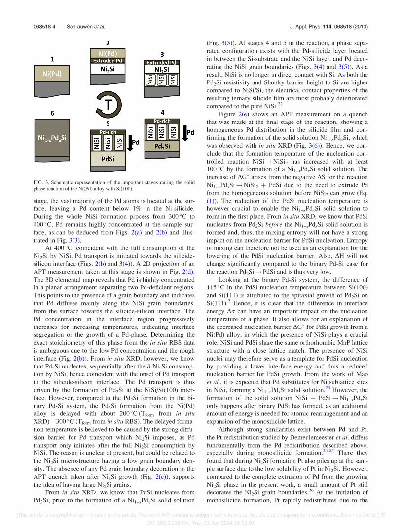
stage, the vast majority of the Pd atoms is located at the sur-
face, leaving a Pd content below 1% in the Ni-silicide.
During the whole NiSi formation process from 300 �C to
400 �C, Pd remains highly concentrated at the sample sur-
face, as can be deduced from Figs. 2(a) and 2(b) and illus-
trated in Fig. 3(3).
At 400 �C, coincident with the full consumption of the
Ni2Si by NiSi, Pd transport is initiated towards the silicide-
silicon interface (Figs. 2(b) and 3(4)). A 2D projection of an
APT measurement taken at this stage is shown in Fig. 2(d).
The 3D elemental map reveals that Pd is highly concentrated
in a planar arrangement separating two Pd-deficient regions.
This points to the presence of a grain boundary and indicates
that Pd diffuses mainly along the NiSi grain boundaries,
from the surface towards the silicide-silicon interface. The
Pd concentration in the interface region progressively
increases for increasing temperatures, indicating interface
segregation or the growth of a Pd-phase. Determining the
exact stoichiometry of this phase from the in situ RBS data
is ambiguous due to the low Pd concentration and the rough
interface (Fig. 2(b)). From in situ XRD, however, we know
that Pd2Si nucleates, sequentially after the d-Ni2Si consump-
tion by NiSi, hence coincident with the onset of Pd transport
to the silicide-silicon interface. The Pd transport is thus
driven by the formation of Pd2Si at the NiSi/Si(100) inter-
face. However, compared to the Pd2Si formation in the bi-
nary Pd-Si system, the Pd2Si formation from the Ni(Pd)
alloy is delayed with about 200 �C ðTform from in situXRD)—300 �C (Tform from in situ RBS). The delayed forma-
tion temperature is believed to be caused by the strong diffu-
sion barrier for Pd transport which Ni2Si imposes, as Pd
transport only initiates after the full Ni2Si consumption by
NiSi. The reason is unclear at present, but could be related to
the Ni2Si microstructure having a low grain boundary den-
sity. The absence of any Pd grain boundary decoration in the
APT quench taken after Ni2Si growth (Fig. 2(c)), supports
the idea of having large Ni2Si grains.
From in situ XRD, we know that PdSi nucleates from
Pd2Si, prior to the formation of a Ni1–xPdxSi solid solution
(Fig. 3(5)). At stages 4 and 5 in the reaction, a phase sepa-
rated configuration exists with the Pd-silicide layer located
in between the Si-substrate and the NiSi layer, and Pd deco-
rating the NiSi grain boundaries (Figs. 3(4) and 3(5)). As a
result, NiSi is no longer in direct contact with Si. As both the
Pd2Si resistivity and Shottky barrier height to Si are higher
compared to NiSi/Si, the electrical contact properties of the
resulting ternary silicide film are most probably deteriorated
compared to the pure NiSi.22
Figure 2(e) shows an APT measurement on a quench
that was made at the final stage of the reaction, showing a
homogeneous Pd distribution in the silicide film and con-
firming the formation of the solid solution Ni1–xPdxSi, which
was observed with in situ XRD (Fig. 3(6)). Hence, we con-
clude that the formation temperature of the nucleation con-
trolled reaction NiSi!NiSi2 has increased with at least
100 �C by the formation of a Ni1–xPdxSi solid solution. The
increase of DG� arises from the negative DS for the reaction
Ni1–xPdxSi!NiSi2 þ PdSi due to the need to extrude Pd
from the homogeneous solution, before NiSi2 can grow (Eq.
(1)). The reduction of the PdSi nucleation temperature is
however crucial to enable the Ni1–xPdxSi solid solution to
form in the first place. From in situ XRD, we know that PdSi
nucleates from Pd2Si before the Ni1–xPdxSi solid solution is
formed and, thus, the mixing entropy will not have a strong
impact on the nucleation barrier for PdSi nucleation. Entropy
of mixing can therefore not be used as an explanation for the
lowering of the PdSi nucleation barrier. Also, DH will not
change significantly compared to the binary Pd-Si case for
the reaction Pd2Si! PdSi and is thus very low.
Looking at the binary Pd-Si system, the difference of
115 �C in the PdSi nucleation temperature between Si(100)
and Si(111) is attributed to the epitaxial growth of Pd2Si on
Si(111).2 Hence, it is clear that the difference in interface
energy Dr can have an important impact on the nucleation
temperature of a phase. It also allows for an explanation of
the decreased nucleation barrier DG� for PdSi growth from a
Ni(Pd) alloy, in which the presence of NiSi plays a crucial
role. NiSi and PdSi share the same orthorhombic MnP lattice
structure with a close lattice match. The presence of NiSi
nuclei may therefore serve as a template for PdSi nucleation
by providing a lower interface energy and thus a reduced
nucleation barrier for PdSi growth. From the work of Mao
et al., it is expected that Pd substitutes for Ni sublattice sites
in NiSi, forming a Ni1–xPdxSi solid solution.23 However, the
formation of the solid solution NiSi þ PdSi!Ni1–xPdxSi
only happens after binary PdSi has formed, as an additional
amount of energy is needed for atomic rearrangement and an
expansion of the monosilicide lattice.
Although strong similarities exist between Pd and Pt,
the Pt redistribution studied by Demeulemeester et al. differs
fundamentally from the Pd redistribution described above,
especially during monosilicide formation.24,25 There they
found that during Ni2Si formation Pt also piles up at the sam-
ple surface due to the low solubility of Pt in Ni2Si. However,
compared to the complete extrusion of Pd from the growing
Ni2Si phase in the present work, a small amount of Pt still
decorates the Ni2Si grain boundaries.26 At the initiation of
monosilicide formation, Pt rapidly redistributes due to the
FIG. 3. Schematic representation of the important stages during the solid
phase reaction of the Ni(Pd) alloy with Si(100).
063518-4 Schrauwen et al. J. Appl. Phys. 114, 063518 (2013)
[This article is copyrighted as indicated in the article. Reuse of AIP content is subject to the terms at: http://scitation.aip.org/termsconditions. Downloaded to ] IP:
160.103.2.236 On: Tue, 21 Jan 2014 15:53:01

incorporation of Pt in the growing NiSi seeds or the forma-
tion of a Pt-silicide. This strongly dissimilar behavior is a
result of the distinct formation temperatures of PdSi (above
730 �C) compared to PtSi and NiSi (both around 300 �C),
allowing direct formation and solid solubility of PtSi and
NiSi, in contrast to PdSi and NiSi.
IV. CONCLUSION
During the Ni(Pd) silicide reaction, phase separation of
the binary NiSi and Pd-silicides occurs. As a result Pd2Si is
in direct contact with Si instead of NiSi, thus deteriorating
the electrical contact properties. This is of major importance
when considering the use of Pd as an additive element in
NiSi contacts. Furthermore, a strong reduction of the binary
PdSi nucleation temperature can be achieved in the presence
of Ni. The effect is qualitatively understood by making use
of the classical nucleation theory. The PdSi formation
at temperatures significantly below the widely accepted
nucleation temperature in the pure Pd-Si system does not
result from the effect of entropy of mixing due to the direct
formation of a Ni1–xPdxSi solid solution, as previously
suggested.8,10–14 Rather, it is triggered by a reduction in sur-
face energy, induced by the presence of the isomorphous
NiSi phase. The coexistence of NiSi and PdSi transforms
into a Ni1–xPdxSi solution at higher temperatures, which in
turn results in an improved monosilicide stability by post-
poning NiSi2 nucleation due to entropy of mixing. The iso-
morphism, and hence the mutual solubility of NiSi and PdSi,
plays a crucial, yet distinct role in the nucleation of PdSi and
NiSi2.
Our work shows that either the interface energy or the
entropy of mixing is decisive for altering the nucleation bar-
rier of PdSi and NiSi2, respectively. These results are more
generally valid, showing that the mutual influence of the two
binary systems significantly alters the reaction parameters in
the ternary system, such as formation temperatures and phase
formation sequence. In other words, knowing the two binary
constituents are insufficient to understand the ternary system.
This paper fills one of the many gaps in assigning the param-
eters that are relevant for the understanding of ternary reac-
tions, i.e., the role of interface energy and entropy of mixing.
ACKNOWLEDGMENTS
This work was supported by the Fund for Scientific
Research, Flanders (FWO), the Concerted Action Program
(GOA/09/006 and GOA/14/007) of the KU Leuven, the
Bilateral Cooperation between Flanders and South Africa
(BIL 04/47), the National research Foundation (South
Africa), and SPIRIT (Contract No. 227012).
1S.-L. Zhang and M. €Ostling, Crit. Rev. Solid State Mater. Sci. 28, 1–129
(2003).2F. M. d’Heurle, J. Mater. Res. 3, 167–195 (1988).3C. Lavoie, F. M. d’Heurle, C. Detavernier, and C. Cabral, Jr.,
Microelectron. Eng. 70, 144–157 (2003).4A. Vantomme, M. F. Wu, S. Hogg, U. Wahl, W. Deweerd, H. Pattyn, G.
Langouche, S. Jin, and H. Bender, Nucl. Instrum. Methods Phys. Res. B
147, 261–266 (1999).5D. Smeets, J. Demeulemeester, K. De Keyser, D. Deduytsche, C.
Detavernier, C. M. Comrie, C. C. Theron, C. Lavoie, and A. Vantomme,
J. Appl. Phys. 104, 093533 (2008).6C. Detavernier, R. L. Van Meirhaeghe, F. Cardon, and K. Maex, Phys.
Rev. B 62, 12045–12051 (2000).7D. Mangelinck, J. Y. Dai, J. S. Pan, and S. K. Lahiri, Appl. Phys. Lett. 75,
1736 (1999).8C. Detavernier, X. P. Qu, R. Van Meirhaeghe, B. Z. Li, and K. Maex,
J. Mater. Res. 18, 1668–1678 (2003).9C. Lavoie, C. Detavernier, C. Cabral, Jr., F. M. d’Heurle, A. J. Kellock, J.
Jordan-Sweet, and J. M. E. Harper, Microelectron. Eng. 83, 2042–2054
(2006).10T. Finstad and M.-A. Nicolet, J. Appl. Phys. 50, 303–307 (1979).11V. Ievlev, E. Shvedov, S. Soldatenko, S. B. Kushchev, and Y.
Gorozhankin, Inorg. Mater. 42, 151–159 (2006).12Y.-C. Kim, P. Adusumilli, L. Lauhon, D. Seidman, S.-Y. Jung, H.-D. Lee,
R. Alvis, R. Ulfig, and J. Olson, Appl. Phys. Lett. 91, 113106 (2007).13A. Karabko, A. Dostanko, J. Kong, and W. Shen, Phys. Status Solidi A
206, 1898–1903 (2009).14M. Putero and D. Mangelinck, Appl. Phys. Lett. 101, 111910 (2012).15B. Y. Tsaur and M.-A. Nicolet, Appl. Phys. Lett. 37, 708–711 (1980).16K. N. Tu, G. Otaviani, and R. D. Thompson, J. Appl. Phys. 53, 4406–4410
(1982).17C. C. Theron, J. A. Mars, C. L. Churms, J. Farmer, and R. Pretorious,
Nucl. Instrum. Methods Phys. Res. B 139, 213–218 (1998).18D. Blavette, A. Bostel, J. Sarrau, B. Deconihout, and A. Menand, Nature
363, 432–435 (1993).19S. Gaudet, C. Coia, P. Desjardins, and C. Lavoie, J. Appl. Phys. 107,
093515 (2010).20F. d’Heurle, C. S. Petersson, J. E. E. Baglin, S. J. La Placa, and C. Y.
Wong, J. Appl. Phys. 55, 4208–4218 (1984).21W. Wopersnow and K. Schubert, Z. Metallkunde 67, 807–810 (1976).22Properties of Metal Silicides, edited by K. Maex and M. Van Rossum
(INSPEC, the Institution of Electrical Engineers, London, United
Kingdom, 1995), p. 165 and p. 193.23Z. Mao, Y.-C. Kim, H.-D. Lee, P. Adusumilli, and D. Seidman, Appl.
Phys. Lett. 99, 013106 (2011).24J. Demeulemeester, D. Smeets, C. Comrie, C. Van Bockstael, C.
Detavernier, K. Temst, and A. Vantomme, J. Appl. Phys. 108, 043505
(2010).25J. Demeulemeester, D. Smeets, C. Van Bockstael, C. Detavernier, C. M.
Comrie, N. P. Barradas, A. Vieira, and A. Vantomme, Appl. Phys. Lett.
93, 261912 (2008).26D. Mangelinck, K. Hoummada, A. Portavoce, C. Perrin, R. Daineche, M.
Descoins, D. J. Larson, and P. H. Clifton, Scr. Mater. 62, 568–571
(2010).
063518-5 Schrauwen et al. J. Appl. Phys. 114, 063518 (2013)
[This article is copyrighted as indicated in the article. Reuse of AIP content is subject to the terms at: http://scitation.aip.org/termsconditions. Downloaded to ] IP:
160.103.2.236 On: Tue, 21 Jan 2014 15:53:01