· list of illustrations ... command block description ... the winchester interface conforms to...
TRANSCRIPT


WD1002S-WX2
Winchester
Disk Controller
OEM 'Manual
Document No.: 79-000029
2445 McCabe Way I rvine, California 92714
(714) 863-0503 (714) 863-0102
TWX 910-595-1139
July 1985

COPYRIGHT © 1985 WESTERN DIGITAL CORP. ALL RIGHTS RESERVED
This document is protected by copyright, and contains information proprietary to Western Digital Corp. Any copying, adaptation, distribution, public performance, or public display of this document without the express written consent of Western Digital Corp. is strictly prohibited. The receipt or possession of this document does not convey any rights to reproduce or distribute its contents, or to manufacture, use, or sell anything that may describe, in whole or in part, without the specific written consent of Western Digital Corp.
ii

TABLE OF CONTENTS
SECTION 1 INTRODUCTION
1.1 Document Scope ................................................... 1-1 1.2 Description ....................................................... 1-1 1.3 Features ......................................................... 1-1 1.4 Operation ........................................................ 1-3
1.4.1 Bi-Directional Control/Data Bus ................................. 1-3 1.4.2 Address Decoding Logic ....................................... 1-3 1.4.3 Configuration Jumpers ........................................ 1-3 1.4.4 Bios ROM .................................................. 1-3 1.4.5 WD 11 COO-17 Logic Array ...................................... 1-3 1.4.6 WD 10C20 Winchester Data Separator and Write
Precompensation Device .......................... ' ............. 1-3 1.4.7 Sector Buffer RAM ..................... ; ..................... 1-3 1.4.8 WD1010A-05 Winchester Disk Controller .......................... 1-4 1.4.9 WD1015 Buffer Manager Control Processor ........................ 1-4 1.4.10 Reset Logic ................................................. 1-4
SECTION 2 SPECIFICATIONS
2.1 General .......................................................... 2-1 2.2 Electrical ......................................................... 2-1
2.2.1 Host Interface ............................................... 2-1 2.2.2 Drive Interface .............................................. 2-1 2.2.3 WD10C20 .................................................. 2-1 2.2.4 Power ..................................................... 2-1
2.3 Physical ................. , ...... , ........................ ' ......... 2-2 2.4 Environmental. ............................................ ' ........ 2-2
SECTION 3 INTERFACE CONNECTIONS
3.1 Organization .. ' .................................................... 3-1 3.2 Host Interface ..................................................... 3-1 3.3 Drive Interface ................................. '; .................. 3-2
3.3.1 Drive Control ............................................... 3-2 3.4 Drive Data Connector ............................................... 3-4
SECTION 4 INTERFACE TIMING
4.1 Tim ing ........................................................... 4-'1
SECTION 5 COMMAND DESCRIPTION
5.1 General .......................................................... 5-1 5.2 I/O Port Description ................................................ 5-2
5.2.1 Port 320 ' ....................... ' ...... , ..................... 5-2 5.2.2 Port 321 ................................................... 5-2 5.2.3 Port 322 ................................................... 5-3 5.2.4 Port 323 ............................... , .................... 5-3
5.3 Command Block .................. , ................................ 5-3 5.4 Test Drive Ready (Class 0, OP CodeOO) ................................. 5-4
5.4. 1 Possible Error Codes .......................................... 5-4
iii

5.5. Recalibrate (Class 0, OP Code 01) ...................................... 5-4 5.5.1 Possible Error Codes .......................................... 5-4
5.6 Read Status of Last Operation (Class 0, OP Code 03) ....................... 5-5 5.7 Format Drive Starting at Desired Track (Class 0, OP Code 04) ................ 5-7
5.7.1 Possible Error Codes .......................................... 5-8 5.7.2 Interleaving ................................................. 5-8
5.8 Verify Sectors (Class 0, OP Code 05) ................................... 5-8 5.8. 1 Possible Error Codes .......................................... 5-8
5.9 Format Track (Class 0, OP Code 06) .................................... 5-9 5.10 Format Bad Track (Class 0, OP Code 07) ................................ 5-9 5.11 Read Sectors (Class 0, OP Code 08) .................................... 5-9
5.11.1 Possible Error Codes .......................................... 5-9 5.12 Write Sectors (Class 0, OP Code OA) .................................... 5-9
5.12.1 Possible Error Codes .......................................... 5-9 5.13 Seek (Class 0, OP Code OB) ........................................... 5-9
5.13.1 Possible Error Codes ........... : .............................. 5-9 5.14 Initialize Drive Parameters (Class 0, OP Code OC) ......................... 5-10 5.15 Read ECC Burst Error Length (Class 0, OP Code 00) .... ~ ................. 5-10 5.16 Read Sector Buffer (Class 0, OP Code OE) .......................... ; ... 5-10 5.17 Write Sector Buffer (Class 0, OP Code OF) .............................. 5-10 5.18 Execute Sector Buffer Diagnostic (Class E, OP Code 00) ................... 5-10
5.18.1 Possible Error Codes ......................................... 5-10 5.19 Execute Drive Diagnostic (Class E, OP Code 03) .......................... 5-10
5.19.1 Possible Error Codes ......................................... 5-10 5.20 Controller Diagnostics (Class E, OP Code 04) ............................ 5-10
5.20.1 WD1010A-05 Test ........................................... 5-11 5.20.2 WD11 COO-17 ECC Test ....................................... 5-11 5.20.3 Sector Buffer Test ........................................... 5-11 5.20.4 WD1015 RAM Test. ......................................... 5-11 5.20.5 WD1015 ROM Test .......................................... 5-11 5.20.6 Possible Error Codes ......................................... 5-11
5.21 Read Long (Class E, OP Code 05) .......... , ......................... 5-11 5.21.1 Possible Error Codes ......................................... 5-11
5.22 Write Long (Class E, OP Code 06) ..................................... 5-11 5.22.1 Possible Error Codes ......................................... 5-11
SECTION 6 THEORY OF OPERATION
6.1 General ......................... '.' ............................... 6-1 6.2 Buses ............................................................ 6-1
6.2.1 Host I nterface Address Bus AO through A 19 ........................ 6-1 6.2.2 Host Interface Data/Command Bus DO through 07 .................. 6-1 6.2.3 WD1002S-WX2 Intraboard Command/Status Bus BOO through BD7 ..... 6-1 6.2.4 WD 1 002S-WX2 I ntraboard Command/Data Bus ADO through AD7 ...... 6-1 6.2.5 WD 1 002S-WX2 I ntraboard Address Bus RAO through RA 10 ........... 6-1
6.3 Bus Protocol 6.3.1 Selection Phase .............................................. 6-3 6.3.2 Command Phase ............................................. 6-3 6.3.3 Data Phase .................................................. 6-3
6.3.3.1 Programmed I/O Data Transfer ........................... 6-3 6.3.3.2 DMA Data Transfer .................................... 6-3
iv

6.4 Device Address Decoder ............................................. 6-4 6.5 Bios ROM ........................................................ 6-4 6.6 Configuration Jumpers .............................................. 6-4 6.7 WD 11 COO-17 Logic Array ............................................ 6-4
6.7.1 Status, Read, and Write Ports ................................... 6-4 6.7.2 Sector Buffer RAM Addressing and Control ........................ 6-4 6.7.3 ECC Circuitry ............................................... 6-5 6.7.4 Reset Timing Circuitry ........................... , ............ 6-5
6.8 WD1015 Buffer Manager Control Processor .............................. 6-5 6.8.1 Exception Handling ........................................... 6-6
6.9 Sector Buffer ...................................................... 6-6 6.10 WD1010A-05 Winchester Disk Controller ................................ 6-6 6.11 WD 1 OC20 Self-Adjusting Data Separator ................................ 6-7
6.11.1 Clock Generator ............................................. 6-7 6.11.2 Write Precompensation Circuit .................................. 6-7 6.11.3 Data Separator .............................................. 6-7
SECTION 7 INSTALLATION
7.1 Hardware and Software Installation .................................... 7-1 7.2 Jumper Installation and Locations ..................................... 7-1 7.3 Bios ROM Installation ............................................... 7-3
v

TABLE
1-1
3-1 3-2 3-3
4-1 4-2 4-3 4-4
5-1 5-2 5-3 5-4 5-5
7-1 7-2
LIST OF TABLES
TITLE PAGE
WD1 015 Description ..................................... ' ................ 1-4
Host Interface Connector (P1) Pin Description ................................. 3-1 Drive Control Connector (J 1) Pin Description ............................... '.' . 3-3 Drive Data Connectors - J2, J3 .......................................... ' .. 3-5
Host I/O or BIOS Read Timing ............................................. 4-1 DMA I/O Read Timing ... ; : .............................................. 4-2 Host I/O Write Timing .................................................... 4-3 DMA I/O Write Timing .............................. ~ ... ' ................• 4-4
Command Summary ..................................................... 5-1' I/O Port Descriptions .................................................... 5-2 Hardware Status ........................................................ 5-2 Stepping Rate Codes ..................................................... 5-4 Controller Returned Error Codes ................................. ' .......... 5-6
Jumper Selectable Options (W1 through W5) .................... : ............. 7-1 SW1 Jumper Block Description ............................................. 7-2
vi

FIGURE
1-1
4-1 4-2 4-3 4-4
5-1 5-2 5-3 5-4
6-2
7-1 7-2
LIST OF ILLUSTRATIONS
TITLE PAGE
WD1002S-WX2 Functional Block Diagram .................................... 1-2
Host I/O or BIOS Read Timing .............................................. 4-1 DMA I/O Read Timing ................................................... 4-2 Host I/O Write Timing .................................................... 4-3 DMA I/O Write Timing ................................................... 4-4
Command Block Description ............................................... 5-3 Four Status Bytes ....................................................... 5-5 Format ............................................................... 5-7 17 Sectors with a 3: 1 Interleave ............................................ 5-8
WD1002S-WX2 Detailed Block Diagram ...................................... 6-2
Jumper Locations ............... " ........................................ 7-3 Bios Rom Socket Connections ............................................. 7-3
vii
SECTION I INTRODUCTION
1.1 DOCUMENT SCOPE
This document provides the user with the information requ ired to design related software drivers and interface connections for efficient use of the WD1002S-WX2 Winchester Disk Controller Board. It is to the user's advantage to become familiar with the following related documents:
WD11COO-17 Logic Array ........... Data Sheet WD10C20 Winchester Data Separator and
Write Precompensation Device .... ~ Data Sheet WD1010-05 Winchester Disk
Controller ..................... Data Sheet WD1010 Winchester Disk
Controller ................ Application Note WD1 015 Buffer Manager Control
Processor ...................... Data Sheet ST-506 Micro Winchester Disk
Interface . . . . . . . . . . . . . . . . . . . . . . . . . ST506 Seagate Technology Scotts Valley, Cal.
1.2 DESCRIPTION
The WD 1 002S-WX2 is a stand-alone, general purpose Winchester Disk Controller. The WD1002SWX2 interfaces up to two Winchester Disk drives and a Host Processor, e.g. an IBM XT.
The Winchester interface conforms to the Seagate Technology ST506 interface. All necessary receivers and drivers are included on the board, allowing direct connection to the disk drive(s).
A separate computer access port enables communications between the Host and disk controller. An 8-bit bi-directional bus and appropriate control signals comprise th is port. Disk read or write data, status information, and command parameters are transferred via th is bus. An on-board data buffer allows bus transfers to be executed independently of the drive's data transfer.
The WD1002S-WX2 is based on a proprietary chip set consisting of the WD11COO-17, .WD1010A-05, WD10C20, and WD1015.
1.3 FEATURES
• 8-BIT BI-DI RECTIONAL BUS HOST INTERFACE
• IBM XT WINCHESTER CONTROLLER EMULATION, IBM PC HOST INTERFACE
1-1
• WD10C20 WINCHESTER DATA SEPARATOR AND WRITE PRECOMPENSATION DEVICE
• WD11COO-17 LOGIC ARRAY
• DATA RATES UP TO 5 MBITS/SEC
• CONTROLSUP TO 2 DRIVES USING SEAGATE TECHNOLOGY ST506
• SUPPORTS DRIVES OF ANY CONFIGURATION UP TO 1024 CYLINDERS AND 16 R/W HEADS WITH THE WD1015-24 OR 8 R/W HEADS WITH THE WD1015-14
• THE CONTROLLED DRIVES NEED NOT BE OF THE SAME CAPACITY OR CONFIGURATION
• ERROR CORRECTION ON DATA FIELD ERRORS, CRC ID FIELD VERIFICATION
• 32 BIT ECC POLYNOMIAL FOR ERROR DETECTION AND CORRECTION
• READ AND WRITE LONG COMMANDS FOR CHECKING ERROR CORRECTION CIRCUITRY
• SELECTABLE AUTOMATIC RETRIES ON ALL ERRORS
• AUTOMATIC RESTORE AND RE-SEEK ON ALL SEEK ERRORS
• AUTOMATIC FORMATTING
• 512 BYTES PER SECTOR
• SECTOR INTERLEAVE CAPABILITY
• MULTIPLE SECTOR READS AND WRITES
• OVERLAPPED SEEK CAPABILITY ON BUFFERED-STEP DRIVES
• SUPPORTS IMPLIED SEEKS ON ALL COMMANDS
• INTERNAL DIAGNOSTICS
• DMA TRANSFER CAPABI L1TY
• SUPPORTS INTERRUPTS, INTERRUPT REQUESTS, AND DMA REQUEST SHARING
• INCLUDES SOCKET FOR USER SUPPLIED 2716,2732, OR 2764 ROM
• BIOS AVAILABLE
1.4 OPERATION
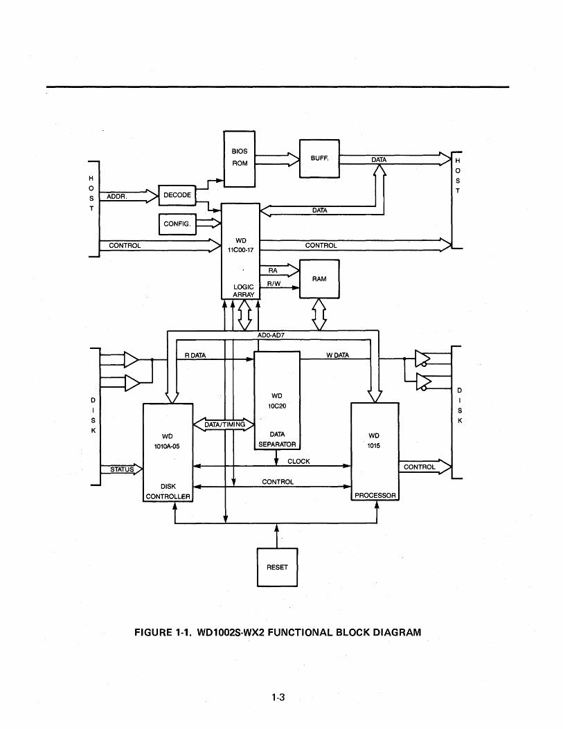
This section provides an operational overview of the WD1002S-WX2 Winchester Disk Controller. For a detailed explanation, refer to Section 6 (Theory of Operation). Asillustrated in Figure 1-1, the WD 1 002S-WX2 consists of the following components:
Bi-directional Control/Data Bus Address Decoding Logic Configu ration Switches Basic Input/Output System (BIOS) ROM WD11COO-17 WD10C20 Sector Buffer RAM WD1010A-05 WD1015 Reset Logic
1.4.1 BI-DIRECTIONAL CONTROL/DATA BUS
The 8-bit, bi-directional bus transmits addresses, commands, data, and status information. This bus I inks the WD 1 002S-WX2 to the Host. Specifically, this bus transmits data between the Host and Sector Buffer RAM.
1.4.2 ADDRESS DECODING LOGIC
The puspose of this logic is to decode a valid device address from the Host.
1.4.3 CONFIGURATION JUMPERS
These jumpers configure the WD1002S-WX2 for different disk drive capacities.
1.4.4 BIOS ROM
The Host, after powering up, interrogates its ports to determine what devices are connected. The Host uses information supplied by the BIOS ROM to perform an install operation. Then, during normal operation, the BIOS operates much like a driver that is resident in the Host's memory space. The BIOS ROM is addressed at Host memory locations C8000-C8FFF. The BIOS is addressed by the AO through A 19 bus. Outputs to the Host are via the Intraboard Command/Status bus (BDO through BD7) and Host Interface Data/Command bus (DO through D7).
1-2
1.4.5 WD11COO-17
The WD11COO-17 incorporates several functions in a single package. Implementation of these functions occurs by combining random logic and specialized circu its. The WD 11 COO-17 contains the following circuits:
Status ports Read and write ports Sector Buffer RAM addressing and control ECC Reset timing
The WD11COO-17 connects directly to the Host I nterface Data/Command and I ntraboard Command/Data (ADO-AD7) buses.
1.4.6 WD10C20
The WD 1 OC20 performs phase-locked loop data synchronization on read data from the Winchester drives. This device also conditions write data to be recorded on the disk. The WD 10C20 includes both frequency and phase detection. Zero phase error start-up circuitry eliminates problems due to asymmetry. The WD10C20 requires no adjustments and contains all data synchronization and write precompensation circuitry in a single device.
1.4.7 SECTOR BUFFER RAM
The Sector Buffer RAM is a 2K x 8 RAM. The Sector Buffer allows Host data transfers independent of the actual drive data transfer rate. The Sector Buffer temporarily stores the following information:
Sector data during Read and Write Commands Disk format information during a Format
Command Drive characteristics during a Set Parameters
Command
BIOS .... .... ~ - ) BUFF. DATA ::> H ROM p-
I\. 0 H • ~
S 0 -"'" T S AD DR. DECODE
p-
T < DATA
l CONFIG. P ~
.. WD .. CONTROL .)
11COO-17 CONTROL ..) ......
- .. RA :>
r RAM LOGIC R/W
ARRAY
'D' D ADO-AD7
- ~ ..... .... RDATA WDATA I;>
~ .. ~
lf~ , V - D
D V WD I
I 10C20
S
S -- ~ K < DATA/TIMING ~ K DATA WD WD
1010A-05 SEPARATOR 1015
~ CLOCK --. CONTROL :> STATUS .) .. -- DISK
CONTROL -"" - -
CONTROLLER PROCESSOR
,Ir
t RESET
FIGURE 1-1. WD1002S-WX2 FUNCTIONAL BLOCK DIAGRAM
1-3
1.4.8 WD1010A-05
. The primary function of the WD1010A-05 is to control data transfers between the disk and the Sector Buffer. Data transfers take place after the WD 1 015 Buffer Manager Control Processor positions the selected head over the desired track. The WD1010A-05 receives the parameters and commands from the WD1015 via the ADO through AD7 bus. The WD 1 01 OA-05 .interprets the parameter or command, determines which sectors are involved, and whether a read, write, or format function is required.
1.4.9 WD1015
The WD1015 manages and controls all commands and communications between the Host and WD1010A-05. The WD1015 controls ECC and CRC functions.
There are two versions of the WD1015. Table 1-1 describes the differences between the two versions of the WD1015. The acronym WD1015 refers to both versions. When a specific reference is made to a specific version, the appropriate acronym is used.
TABLE 1-1. WD1015 DESCRIPTION
FUNCTION WD1015-14 WD1015-24
Execution of automatic Yes No self-test after Reset command or power-up
Supports 16 heads No Yes
3.5 seconds time-out on No Yes single track steps
Bit 4 of opcode in Valid Don't care Command Control
Step rates
Format Bad Track
1.4.10 RESET LOGIC
The Reset Logic initializes the internal circuitry of the WD1002S-WX2 during the power-up process or a low voltage condition. The Reset Logic also disables the WRITE GATE signal. Disabling WR ITE GATE prevents writing spurious data to the disk drive during power up, power down or a low voltage condition. .
1-4
REMARKS
The WD1015-14 supports up to eight heads. The WD1015-14 uses the REDUCED WRITE CURRENT (RWe) signal. The WD1015-24 supports up to 16 heads. The WD 1 015-24 uses the RWC pin on J1 as HEAD SELECT 3 (HS3). Refer to Sections 3 and 7 for further details.
3.5 seconds time-out allows removable/servo drives time to create servo map. WD1015-14 allows 1 second.
Refer to Section 5 for further details.
Refer to Section 5 for further details.
Refer to Section 5 for further details.

SECTION II SPECIFICATIONS
2.1 GENERAL
This section contains the overall specifications for the WD1002S-WX2 Winchester Disk Controller.
2.2 ELECTRICAL
2.2.1 HOST INTERFACE Type Max Cable Length
2.2.2 DRIVE INTERFACE Encoding Method Cylinders per Drive Sectors per Track Bytes per Sector Heads
Drive Selects Stepping Rates
Data Transfer Rate Write Precomp Time Sectoring CRC Polynomial ECC Polynomial
Reciprocal ECC Polynomial
Miscorrection Prob. Non-detection Prob. Correction Span Max Cable Length:
Control (Total Daisy Chain) Data (Radial-each)
2.2.3 WD10C20
Acqu isition Time Captu re Range Bit Jitter Tolerance Asymmetry Tolerance
2.2.4 POWER
Voltage Current Ripple Voltage Current
2-1
IBM PC Connects directly to Host motherboard with a 62 pin card edge connector
MFM Up to 1024 17 512 8 with WD1015-14 16 with WD1015-24 2 70IJsec, 200IJsec, 3msec (WD 1 015-14) 18 jJsec,30 J-Isec, 45J-1sec, 60jJsec, 75IJsec, 210IJsec, 3msec (WD1015-24) 5Mbits/sec (ST506) 12nsec Soft X16+X12+X5 +1 X32 + X28 + X26 + X19 + X17 + X10 + X6 + X2 + 1 X32 + X30 + X26 + X22 + X15+X13+X6 +X4 +1 5 bit correction = < 1.6 E-5 <2.3E-10 Up to 11-bit burst
3 meters (10ft.) 3 meters (10 ft.)
< or = 12.81Js ± 2.2% to 1 ns after 12.8jJs acquisition ± -34ns (min. of 40 db after acquisition) 34ns (write precompensation turned off; as measu red over constant R C LK pattern)
5V ±5% 0.8 amps max. 0.1 volts max., 25 mV typical +12V ±10% 10 rnA. max.
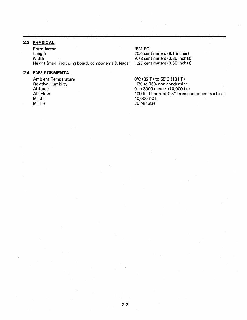
2.3 PHYSICAL
Form factor Length Width Height (max. including board, components & leads)
2.4 ENVIRONMENTAL
Ambient Temperature Relative Humidity Altitude Air Flow MTBF MTTR
2-2
IBM PC 20.6 centimeters (8.1 inches) 9.78 centimeters (3.85 inches) 1.27 centimeters (0.50 inches)
O°C (32°F) to 55°C (131°F) 10% to 95% non-condensing o to 3000 meters (10,000 ft.) 100 lin ft/min. at 0.5" from component surfaces. 10,000 POH . 30 Minutes
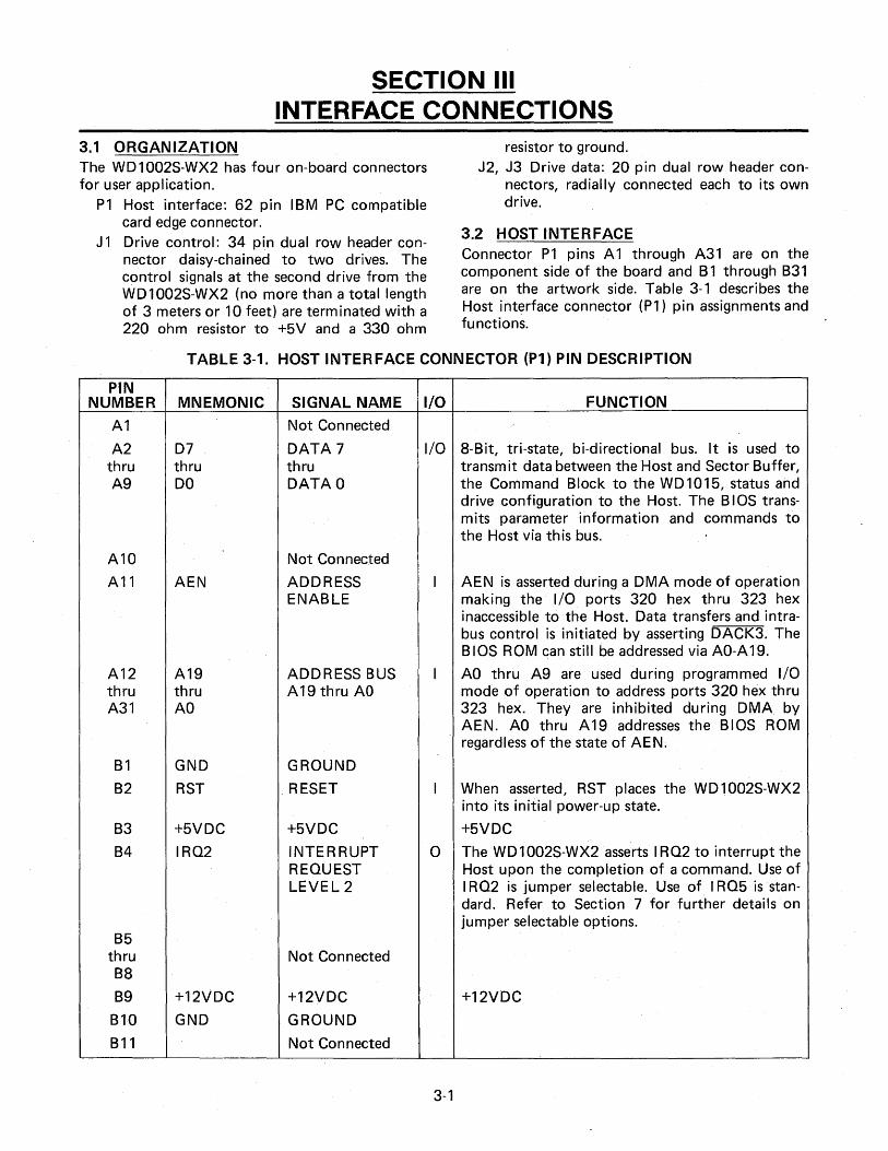
SECTION III INTERFACE CONNECTIONS
3.1 ORGANIZATION The WD 1 002S-WX2 has four on-board connectors for user application.
P1 Host interface: 62 pin IBM PC compatible card edge connector.
J 1 Drive control: 34 pin dual row header connector daisy-chained to two drives. The control signals at the second drive from the WD1002S-WX2 (no more than a total length of 3 meters or 10 feet) are terminated with a 220 ohm resistor to +5V and a 330 ohm
resistor to ground. J2, J3 Drive data: 20 pin dual row header con
nectors, radially connected each to its own drive.
3.2 HOST INTERFACE Connector P1 pins A 1 through A31 are on the component side of the board and B 1 through B31 are on the artwork side. Table 3-1 describes the Host interface connector (P1) pin assignments and functions.
TABLE 3-1. HOST INTERFACE CONNECTOR (P1) PIN DESCRIPTION
PIN NUMBER MNEMONIC SIGNAL NAME I/O FUNCTION
A1 Not Connected
A2 07 DATA 7 I/O 8-Bit, tri-state, bi-directional bus. It is used to thru thru thru transm it data between the Host and Sector Buffer, A9 DO DATA 0 the Command Block to the WD1015, status and
drive configuration to the Host. The B I OS trans-mits parameter information and commands to the Host via this bus.
A10 Not Connected
A 11 AEN ADDRESS I AEN is asserted during a DMA mode of operation ENABLE making the I/O ports 320 hex thru 323 hex
inaccessible to the Host. Data transfers and intra-bus control is initiated by asserting DACK3. The B IDS ROM can still be addressed via AO-A 19.
A12 A19 ADDRESS BUS I AO thru A9 are used during programmed I/O thru thru A19thruAO mode of operation to address ports 320 hex thru A31 AO 323 hex. They are inhibited during DMA by
AEN. AO thru A19 addresses the BIOS ROM regardless of the state of AEN.
B1 GND GROUND
B2 RST RESET I When asserted, RST places the WD 1002S-WX2 into its initial power-up state.
B3 +5VDC +5VDC +5VDC
B4 IRQ2 INTERRUPT 0 The WD1 002S-WX2 asserts I RQ2 to interrupt the REQUEST Host upon the completion of a command. Use of LEVEL 2 I RQ2 is jumper selectable. Use of I RQ5 is stan-
dard. Refer to Section 7 for further details on jumper selectable options.
B5 thru Not Connected B8
B9 +12VDC +12VDC +12VDC
B10 GND GROUND
B11 Not Connected
3-1
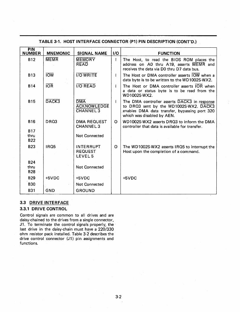
TABLE 3-1. HOST INTERFACE CONNECTOR (P1) PIN DESCRIPTION (CONT'D.)
PIN NUMBER MNEMONIC
B12 MEMR
B13 lOW
B14 lOR
B15 DACK3
B16 DRQ3
B17 thru B22
B23 IRQ5
B24 thru B28
B29 +5VDC
B30
B31 GND
3.3 DRIVE INTERFACE
3.3.1 DRIVE CONTROL
SIGNAL NAME I/O
MEMORY I READ
I/O WRITE I
I/O READ I
DMA I ACKNOWLEDGE CHANNEL3
DMA REQUEST 0 CHANNEL3
Not Connected
INTERRUPT 0 REQUEST LEVEL 5
Not Connected
+5VDC
Not Connected
GROUND
Control signals are common to all drives and are daisy-chained to the drives from a single connector, J 1. To terminate the control signals properly, the' last drive in the daisy-chain must have a 220/330 ohm resistor pack installed. Table 3~2-describes the drive control connector (J 1) pin assignments and functions.
3-2
FUNCTION
The Host, to read the BIOS ROM places the address on AO thru A19, asserts MEMR and receives the data via DO thru D7 data bus.
The Host or DMA controller asserts lOW when a data byte is to be written to the WD1002S-WX2.
The Host or DMA controller asserts lOR when a data or status byte is to be read from the WD1002S-WX2.
The DMA controller asserts DACK3 in response to D RQ3 sent by the WD 1 002S-WX2. DACK3
. enables DMA data transfer, bypassing port 320 which was disabled by AEN.
WD 1 002S-WX2 asserts D RQ3 to inform the DMA controller that data is available for transfer.
The WD 1 002S-WX2 asserts I RQ5 to interrupt the Host upon the completion of a command.
+5VDC
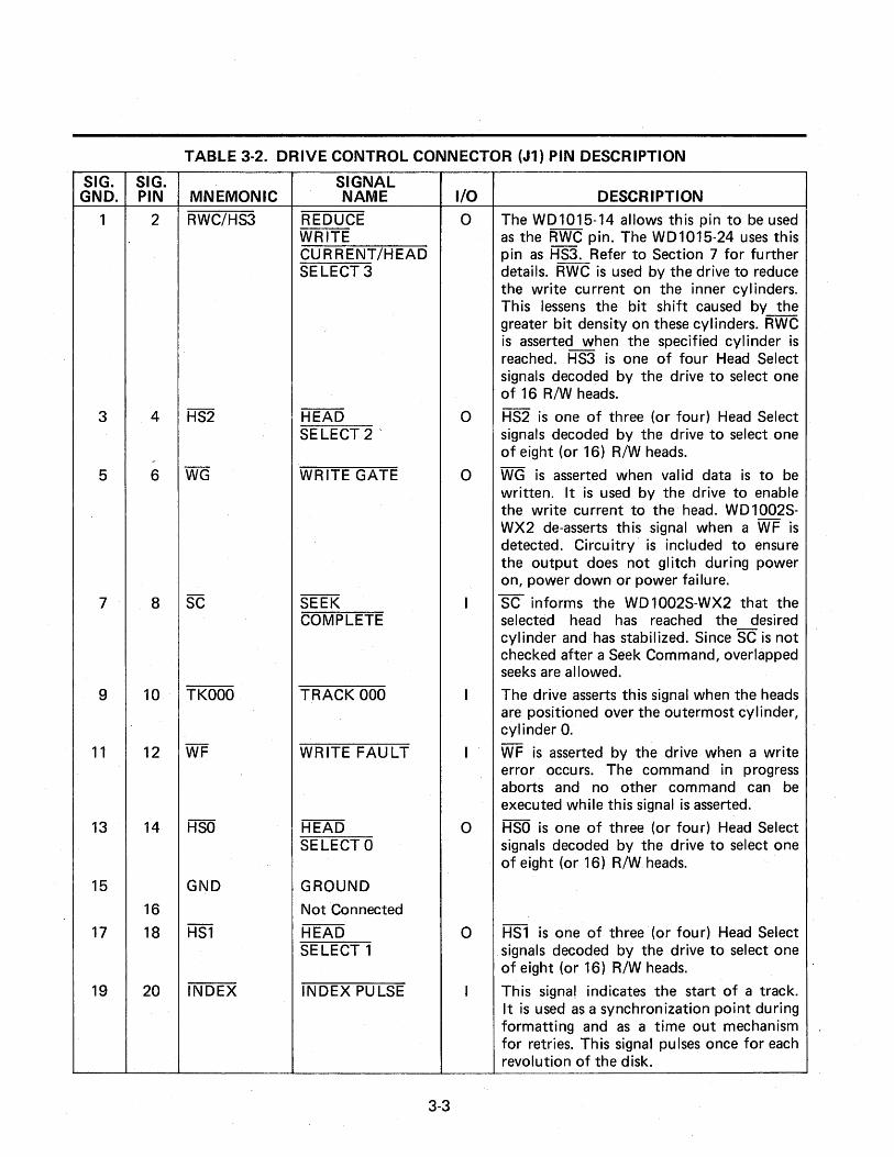
TABLE 3-2. DRIVE CONTROL CONNECTOR (J1) PIN DESCRIPTION
SIG. SIG. GND. PIN MNEMONIC
1 2 RWC/HS3
3 4
5 6
7 8
9 10 TKOOO
11 12
13 14
15 GND
16
17 18 HS1
19 20 INDEX
SIGNAL NAME
REDUCE WRITE CURRENT/HEAD SELECT 3
HEAD SELECT 2 '
WRITE GATE
COMPLETE
TRACK 000
WRITE FAULT
HEAD SELECT 0
GROUND
Not Connected
HEAD SELECT 1
INDEX PULSE
I/O
o
o
o
o
o
3-3
DESCR IPTION
The WD1015-14 allows this pin to be used as the RWC pin. The WD1015-24 uses this pin as HS3. Refer to Section 7 for further details. RWC is used by the drive to reduce the write current on the inner cyl inders. This lessens the bit shift caused by the greater bit density on these cylinders. RWC is asserted when the specified cylinder is reached. HS3 is one of four Head Select signals decoded by the drive to select one of 16 R/W heads.
HS2 is one of three (or four) Head Select signals decoded by the drive to select one of eight (or 16) R/W heads.
WG is asserted when val id data is to be written. It is used by the drive to enable the write current to the head. WD1002SWX2 de-asserts this signal when a WF is detected. Circuitry is included to ensure the output does not glitch during power on, power down or power failure.
SC informs the WD 1002S-WX2 that the selected head has reached the desired cylinder and has stabilized. Since SC is not checked after a Seek Command, overlapped seeks are allowed.
The drive asserts this signal when the heads are positioned over the outermost cylinder, cylinder O.
WF is asserted by the drive when a write error occu rs. The command in progress aborts and no other command can be executed while this signal is asserted.
HSO is one of three (or four) Head Select signals decoded by the drive to select one of eight (or 16) R/W heads.
HS1 is one of three (or four) Head Select signals decoded by the drive to select one of eight (or 16) R/W heads.
This signa! indicates the start of a track. It is used as a synchronization point during formatting and as a time out mechanism for retries. This signal pulses once for each revolution of the disk.
TABLE 3-2. DRIVE CONTROL CONNECTOR (J1) PIN DESCRIPTION (CONT',o.)
SIG. SIG. SIGNAL GND. PIN MNEMONIC NAME
21 22 DRDY DRIVE READY
23 24 STEP STEP PULSE
25 26 DSELO DRIVE SELECT 0
27 28 DSEL 1 DRIVE SELECT 1
29 thru Not Connected 32
33 34 DIRIN DIRECTION IN
3.4 DRIVE DATA CONNECTOR
The data is differential in nature and must be connected to each drive with its own cable, drive 0 to J2 and drive 1 to J3. It shou Id be a flat ribbon cable, or twisted pair, less than 3 meters nO feet) in length. The connector is a 20 pin vertical header on 0.25 centimeter (0.1 inch) center. Table 3-3 describes the drive data connectors (J2 and J3) pin assignments and functions.
I/O DESCRIPTION
I The drive asserts th is signal when the motor is up to speed. No Read or Write com-mands can be performed if this signal is not asserted.
0 STEP, along with DI RIN, positions the heads to the desired cylinder. STEP pulses the stepping motor at the rate specified by the SP bits in the Command Block and is controlled by the WD1015. DIRIN spec-ifies the direction.
0 DSE LOis the decoded output of the SD H Register within the WD1010A-05, latched and sent to the drive by the WD 1 015 to select drive O.
0 DSE L 1 is the decoded output of the SD H Register within the WD1010A-05, latched and sent to the drive by the WD1015 to select drive 1.
0 DIRIN determines the direction the R/W heads take when stepped. Asserted = in, de-asserted = out.
3-4
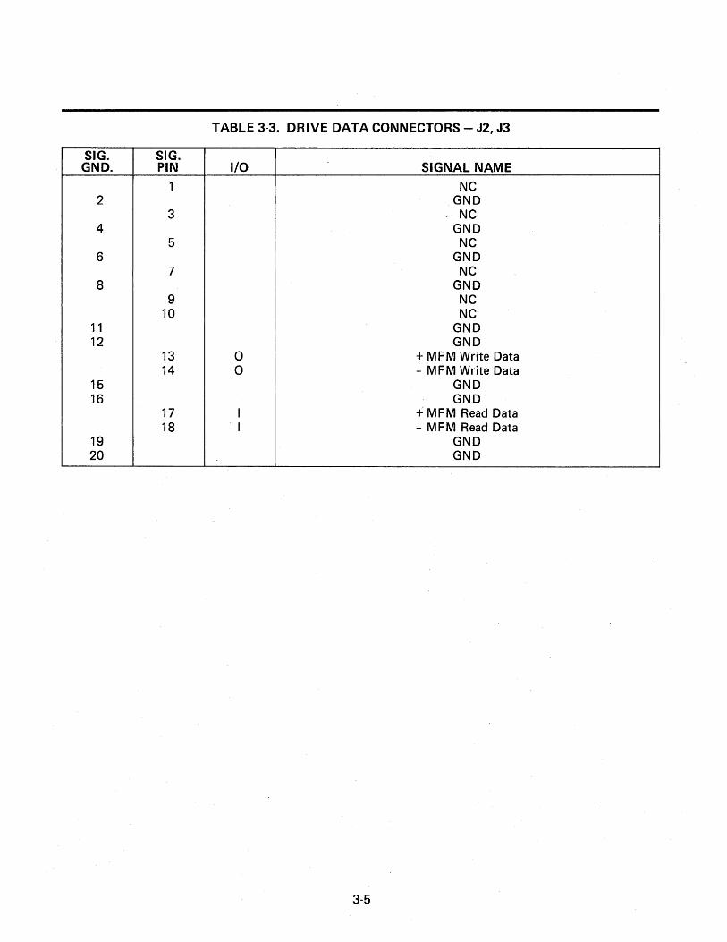
TABLE 3-3. DRIVE DATA CONNECTORS ~ J2, J3
SIG. SIG. GND. PIN I/O SIGNAL NAME
1 NC 2 GND
3 NC 4 GND
5 NC 6 GND
7 NC 8 GND
9 NC 10 NC
11 GND 12 GND
13 0 + M F M Write Data 14 0 - MFM Write Data
15 GND 16 GND
17 I ,.: MFM Read Data 18 I - MFM Read Data
19 GND 20 GND
3-5


4.1 TIMING
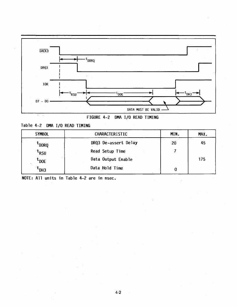
SECTION IV INTERFACE TIMING
Timing diagrams are shown in Figures 4-1 through 4-4 and their values are listed in Tables 4-1 through 4-4 respectively. Since the Controller I/O ports can be accessed by either the Host system DMA Controller or the Host processor, timing is given
for both cases. The processor executes I/O and memory reads from the ports and the on-board B IDS ROM, and writes to the ports. DMA is used for data transfers between the data I/O port and the Host RAM.
:~~AO'--~~~ _________________ AD_D_RE_S_S_W_IL_L __ BE __ VA_L_IO ________________ -')x(~ ____ _
lOR , MEMR --------. I I
~tAS1-i~ ......... !-----tOE ------;·~I
07 _ DO --------..... /E-----------------c/ DATA MUST I ~ ~ BE VALID
I_ tACC(BIOS)
FIGURE 4-1 HOST I/O OR BIOS READ TIMING
TABLE 4-1 HOST I/O OR BIOS READ TIMING
SYMBOL CHARACTERISTIC
t AS1 Address Setup Time
t ACC Address Access Time (BIOS)
tOE Output Enable Time
tDH1 Data Hold Time
NOTE: All units in Table 4-1 are in nsec.
4-1
MIN. MAX.
50
250
175
0
OACK3 ---,~ ________________________________________ ~
I· .. I tOORQ
ORQ3 -----.1 ~--------------------------------------~
lOR I
j..-tRsu-......... I·t-------tooE .. I f.-tOH3 --+1 y,----------(...,.--~)-------.,
07 - 00 -----...... ,~_----------< ~ --= 7 DATA MUST BE VALID ~
FIGURE 4-2 DMA I/O READ TIMING
Table 4-2 DMA 1/0 READ TIMING
SYMBOL CHARACTERISTIC
tDDRQ DRQ3 De-assert Delay
t RSU Read Setup Time
t DOE Data Output Enable
t DH3 Data Hold Time
NOTE: All units in Table 4-2 are in nsec.
4-2
MIN. MAX.
20 45
7
175
0

A19-AO, --< AEN ~-----------__________________________________ -J ADDRESS WILL BE VALID X t ASU2-t-t ........ f------l ...... t-------·1'" twp ·1
lOW ---------.... I I I ... tosu ·1 ... ·1 tOH2
~ ~ 07 - DO----------~--------~ DATA WILL BE VALID > FIGURE 4-3 HOST I/O WRITE TIMING
TABLE 4-3 HOST I/O WRITE TIMING
SYMBOL CHARACTERISTIC MIN.
t ASU2 Address Setup Time 50
twp Write Pulse Time (I/O) 100
t DSU Data Setup Time 50
tDH2 Data Hold Time 0
NOTE: All units in Table 4-3 are in nsec.
4-3

D~K3 ---,~ __________________________________________ ~
I- ~ t tOORQ2
OOQ3 I I~ ____________________________________________ ~ I+- twsu--l"~I ..... -------twp--------l~"1
lOW I 1 .... ------
.... I .. t-----tos .. I .. tOH4--.J 07 - OO------------<C~::::::::::'~~ ________ OA_T_A_WI_l_l_B_E_VA_l_IO ________ -':>~------
FIGURE 4-4 DMA I/O WRITE TIMING TABLE 4-4 DMA I/O WRITE TIMING
SYMBOL CHARACTERISTIC
tDDRQ DRQ3 De-assert Delay
t wsu Write Setup Time
twp Write Pulse Width
t DS Data Setup Time
tDH4 Data Hold Time
NOTE: All units in Table 4-4 are in nsec.
4-4
MIN. MAX.,
20 45
7
100
50
0

5.1 GENERAL
SECTION V COMMAND DESCRIPTION
Th is section provides a detailed description of the Command Block format and function of the 19 commands supported by the WD 1 002S-WX2. Fourteen of the commands are operational and
five are diagnostic. An explanation of how the commands perform their function is discussed in Section 6· Theory of Operation. Table 5-1 I ists a summary of the commands.
TABLE 5-1. COMMAND SUMMARY
PARAMETERS (Refer to Figure 5-1)
COMMAND OP CODE DRV· HD CYL SEC BLK/INT R1 R2 STEP
TEST DRIVE READY 00 V n n n n n n n
RECALIBRATE 01 V n n n n V n n
READ STATUS OF 03 V n
lAST OPERATION n n n n n n
FORMAT DRIVE 04 V V V DR V (INT) V n V
VERIFY SECTORS 05 V V V V V (BlK) V V V
FORMAT TRACK 06 V V V DR V (I NT) V n V
FORMAT BAD TRACK 07 V V V DR V (INT) V n V
READ SECTORS 08 V V V V V (BlK) V V V
WRITE SECTORS OA V V V V V (BlK) V n V
SEEK OB V V V DR n V n V
INITIALIZE DRIVE OC
PARAMETERS V n n n n n n n
READ ECC BURST OD V
ERROR lENGTH n n n n n n n
READ SECTOR BUFFER' OE n n n n n n n n
WRITE SECTOR BUFFER OF n n n n n n n n
EXECUTE SECTOR EO
BUFFER DIAGNOSTIC n n n n n n n n
EXECUTE DRIVE E3
DIAGNOSTIC V n n n n V n V
EXECUTE CONTROllER E4 DIAGNOSTIC
n n n n n n n n
READ lONG E5 V V V V V (BlK) V n V
WRITE lONG E6 V V V V V (BlK) V n V
LEGEND:
V Must be a valid parameter. DR Not used but must be within a valid parameter range. n Not used (should be 0 for future compatibility). INT Interleave B lK Block Count
5-1
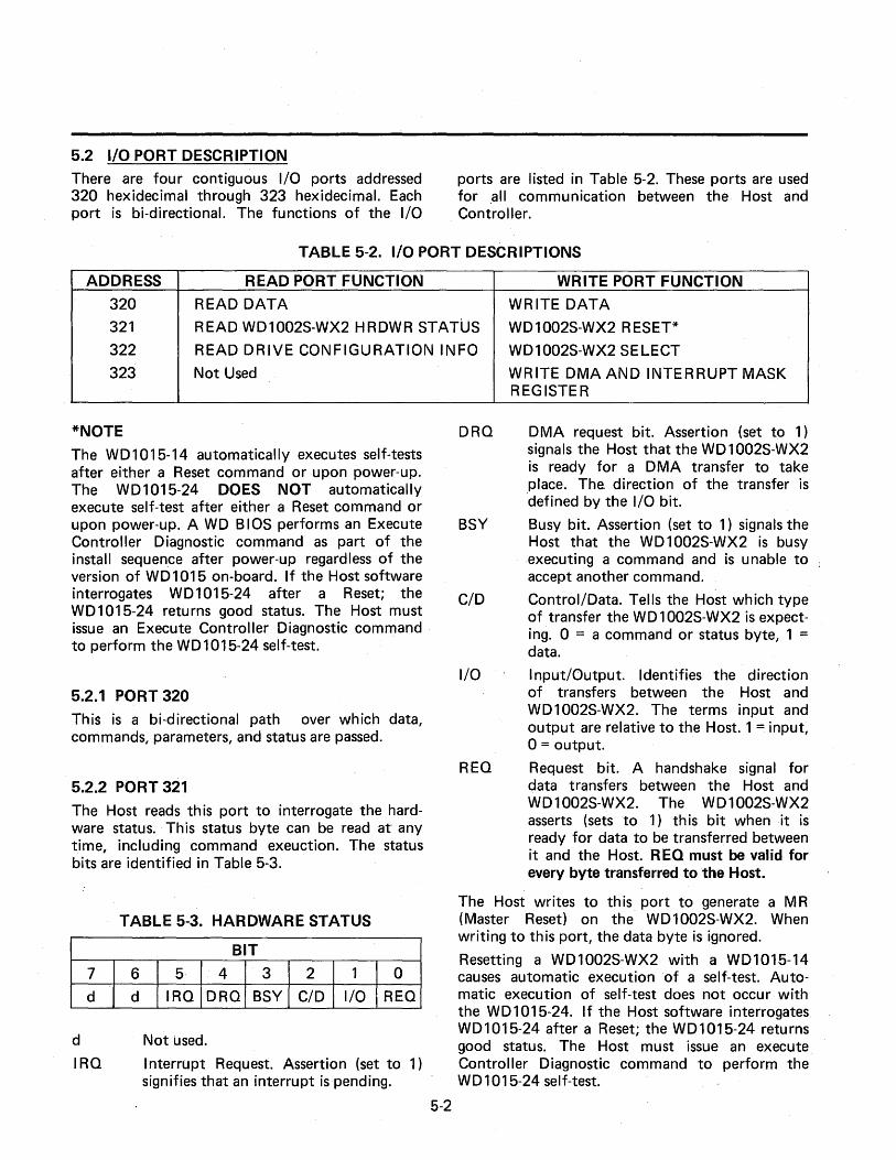
5.2 I/O PORT DESCRIPTION
There are four contiguous I/O ports addressed 320 hexidecimal through 323 hexidecimal. Each port is bi-directional. The functions of the I/O
ports are listed in Table 5-2. These ports are used for ,all communication between the Host and
, Controller.
TABLE 5-2. I/O PORT DESCRIPTIONS
ADDRESS READ PORT FUNCTION WRITE PORT FUNCTION
320 READ DATA WRITE DATA
321 READ WD1002S-WX2 HRDWR STATUS WD1002S-WX2 RESET*
322 READ DRIVE CONFIGURATION INFO WD 1 002S-WX2 SE LECT
323 Not Used
*NOTE
The WD1015-14 automatically executes self-tests after either a Reset command or upon power-up. The WD1015-24 DOES NOT automatically execute self-test after either a Reset command or upon power-up. A WD B lOS performs an Execute Controller Diagnostic command as part of the install sequence after power-up regardless of the version of WD 1 015 on-board. If the Host software interrogates WD 1 015-24 after a Reset; the WD1015-24 returns good status. The Host must issue an Execute Controller Diagnostic command· to perform the WD 1 015-24 self-test.
5.2.1 PORT 320
This is a bi-directional path over which data, commands, parameters, and status are passed.
5.2.2 PORT 321
The Host reads this port to interrogate the hardware status. This status byte can be read at any time, including command exeuction. The status bits are identified in Table 5-3.
7
d
d
IRO
TABLE 5-3. HARDWARE STATUS
6
d
BIT
5 4 3 2 1 0
IRO DRO BSY C/D I/O REO
Not used.
I nterrupt Request. Assertion (set to 1) signifies that an interrupt is pending.
5-2
DRO
BSY
C/D
I/O
REO
WRITE DMA AND INTERRUPT MASK REGISTER
DMA request bit. Assertion (set to 1) signals the Host that the WD 1 002S-WX2 is ready for a DMA transfer to take place. The direction of the transfer is defined by the I/O bit.
Busy bit. Assertion (set to 1) signals the Host that the WD 1 002S-WX2 is busy executing a command and is unable to accept another command.
Control/Data. Tells the Host which type of transfer the WD 1 002S-WX2 is expecting. 0 = a command or status byte, 1 = data.
I nput/Output. Identifies the direction of transfers between the Host and WD1002S-WX2. The terms input and output are relative to the Host. 1 = input, 0= output.
Request bit. A handshake signal for data transfers between the Host and WD1002S-WX2. The WD1002S-WX2 asserts (sets to 1) this bit when it is ready for data to be transferred between it and the Host. R EQ must be valid for every byte transferred to the Host.
The Host writes to th is port to generate a M R (Master Reset) on the WD1002S-WX2. When writing to this port, the data byte is ignored.
Resetting a WD1002S-WX2 with a WD1015-14 causes automatic execution of a self-test. Automatic execution of self-test does not occur with the WD1015-24. If the Host software interrogates WD1015-24 after a Reset; the WD1015-24 returns good status. The Host must issue an execute Controller Diagnostic command to perform the WD 1 015-24 self-test.

5.2.3 PORT 322
Reading Port 322 returns a 4-bit drive configuration code in bits 0 through 3. The two least significant bits correspond to drive 1, the two most significant bits to drive O. The configuration of these bits is established with jumpers on the controller at SW1. Western Digital sets the configuration jumpers to one. Section 7 shows how to set them up for a specific drive.
The two bits associated with each drive is capable of addressing one of four different configuration tables. Both drives can address the same or different tables. The table requ ired by the drive is determined by its formatted capacity. Table 0 = 5MB, 1 = 24MB, 2 = 15MB, 3 = 10MB (default table) with 62-000042-01 and 62-000042-11 WD BIOS. Table 0 = 20MB, Table 1 = 10MB, Table 2 = 20MB, Table 3 = 10MB (default table) with 62-000042-12 WD BIOS.
The parameters established by these tables are:
Number of Cylinders Number of Heads The Starting Cylinder for RWC (Reduced Write
Current). The Starting Cylinder for Write Precomp Maximum Correctable Error Burst Length Retries Allowed, Stable or Immediate ECC
Correction, Step Rate.
Writing to port 322 selects the WD 1 002S-WX2, sets the Busy bit in the Status Register and prepares it to receive a command. When writing to port 322, the data byte is ignored.
5.2.4 PORT 323
Reading this port has no function.
Writing to this port controls the enabling of the interrupt and DMA request signals to the Host. The bits in this port are defined as follows:
BIT
7 6 5 4 3 2 1 0
d d d d d d IROEN DROEN
I ROEN Interrupt Request Enable. When asserted (set to one), enables interrupts to the Host.
DROEN DMA Request Enable. When asserted (set to one), enables DMA requests to the Host.
d Not used.
5-3
5.3 COMMAND BLOCK
The Host first selects the WD 1 002S-WX2 by asserting /lOW while at the same time addressing port 322 with the AO through A 19· address bus. The WD1002S-WX2 then asserts the BSY (BUSY) bit in the Status Register. The Host by asserting IIOR and addressing port 321 reads the status, finding REO asserted transmits the first byte of the six byte Command Block to the WD1015. REO is de-asserted for the second byte of the Command Block transfer. Assertion and de-assertion of REO must occur for each byte transferred. Figure 5-1 defines the bytes within the Command Block, Table 5-1 is a summary of the commands, Section 6 Theory of Operation explains the hand shake between the Host and WD1002S-WX2 while loading the Command Block in the WD1015.
BITS
BYTE 7 I 6 I 5 4 I 3 I 2 I 1 I 0
0 OP CODE
1 0 10iD HEAD NUMBER
2 CYLINDER SECTOR NUMBER
NUMBER MSB
3 CYLINDER NUMBER LSB
4 BLOCK COUNT OR INTERLEAVE
5 R1 I R2 I 0 o I 0 I SP I SP I SP
FIGURE 5-1. COMMAND BLOCK DESCRIPTION
OP Code:
NOTE
Operation Code identifies the type and fu nction of the command. Bits 7, 6, and 5 designate whether the command is operational (0) or diagnostic (E). Bits 4 through 0 select the function of the command, i.e. Read, Write, etc.
The WD1015-24 firmware ignores bit four of byte o (op code).
D Drive number, selects one of two drives zero or one.
Head Number Designates the head to be used on the selected drive. 0 through 15. Selection of heads eight through 15 requires WD1015-24.

Cylinder Number MSB and LSB
Designates the cylinder containing the sector(s) to be used by the command. 0 through 1024.
Sector Number Specifies the starting sector used by 'the command.
Block Count or Interleave
R1
R2
SP
Block count specifies the number of sectors to be used by a Read, Write, Read Long, or Write Long command. A block count of zero equals 256 sectors. I nterleave is used by the Format commands. The maximum interleave is equal to the sectors-per-track minus one. (See Section 5.7.2 for an· explanation of interleaving.)
General disk error retry disable bit. R 1 controls the retry for all errors except a Data ECC error. With R1 asserted the WD1002SWX2 makes no attempt to retry an error operation. Instead it aborts the command and sets the appropriate status in the Status Register. Because the disk is soft sectored an I D field error may cause the WD1002S-WX2 to _ .. _--_. -----
retry for two disk revolutions. With R 1 de-asserted, the WD 1002S-WX2 retries the operation for ten disk revolutions before aborting the command and setting the status bit. I n the case of an I D Not Found Error the WD1002S-WX2 does a restore to track zero and seeks back to the desired track after the first ten disk revolutions and retries for ten disk revolutions before aborting and setting the error status.
ECC Error retry bit. With R2 = 1 an attempt is made to correct the error on the first syndrome. R2 = o there must be two consecutive like syndromes before an attempt is made to correct the error.
The Step Code is used to select the rate at wh ich step pu Ises are issued to the drive. Table 5-4 defines the rates corresponding to each step pu Ise code.
5-4
TABLE 5-4. STEPPING RATE CODES
BITS STEPPING RATES
2 1 0 WD1015-14 WD1015-24
0 0 0 3 msec. per step* 3 msec. per step*
0 o 1 3 msec. per step 45J,Jsec. per step
0 1 0 3 msec. per step 60~sec. per step
o 1 1 3 msec. per step 18J,Jsec. per step
1 0 0 200J,Jsec. per step 210J,Jsec. per step
1 o 1 70J,Jsec. per step 75J,Jsec. per step
1 1 0 3 msec. per step 30J,Jsec. per step
1 1 1 3 msec. per step 18~sec. per step
* Th is is the preferred 3 msec. step code.
5.4 TEST DRIVE READY (CLASS 0, OP CODE 00)
This command selects the drive specified by the D RV bit in the Command Block and interrogates the DRDY, WF, and SC signals returned by that drive. If WF and SC are de-asserted and DRDY asserted, the command returns an error code of 00 No Error Detected.
5.4.1 POSSIBLE ERROR CODES
03 Write Fault 04 Drive Not Ready 08 Drive Still Seeking
5.5 RECALIBRATE (CLASS 0, OP CODE 01)
This command moves the Read/Write heads to track O. The SC signal from the drive controls the stepping rate of this command. Therefore, this command is slower than commands that implement the implied seek and make use of the stepping rate designated by the SP bits in the Command Block.
NOTE Timeout on each step during a Recalibrate command is 1 second with a WD1015-14. Timeout on each step during a Recalibrate is 3.5 seconds with a WD 1 015-24. The 3.5 second timeout supports removable Winchesters.
5.5.1 POSSIBLE ERROR CODES
03 Write Fault 04 Drive Not Ready 06 Track Zero Not Found
5.6 READ STATUS OF LAST OPERATION (CLASS 0, OP CODE 03)
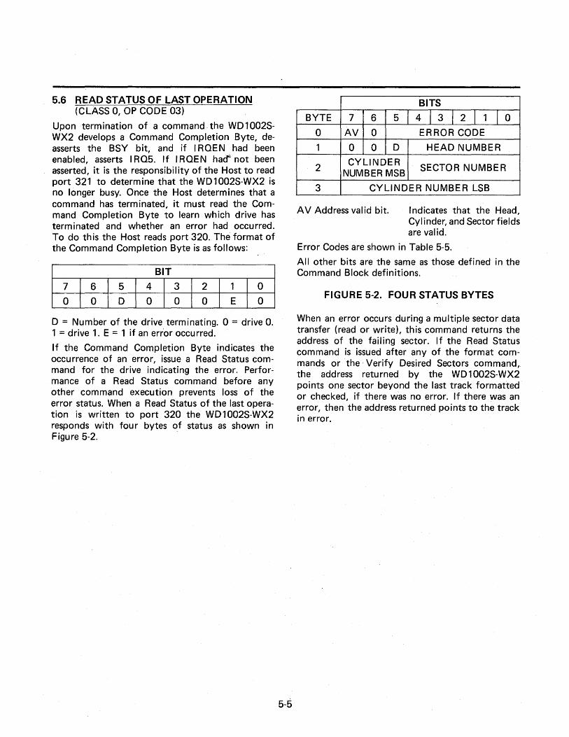
Upon termination of a command. the WD1002SWX2 develops a Command Completion Byte, deasserts the BSY bit, and if I ROEN had been enabled, asserts I RQ5. If I ROEN ha<f not been asserted it is the responsibility of the Host to read port 321 to determine that the WD1002S-WX2 is no longer busy. Once the Host determines that a command has terminated, it must read the Command Completion Byte to learn which drive has terminated and whether an error had occurred. To do this the Host reads port 320. The format of the Command Completion Byte is as follows:
D = Number of the drive terminating. 0 = drive O. 1 = drive 1. E = 1 if an error occurred.
If the Command Completion Byte indicates the occurrence of an error, issue a Read Status command for the drive indicating the error. Performance of a Read Status command before any other command execution prevents loss of the error status. When a Read Status of the last operation is written to port 320 the WD 1 002S-WX2 responds with four bytes of status as shown in Figure 5-2.
5-5
BITS
BYTE 7 6 5 4 I 3 I 2 I 1 T 0
0 AV 0 ERROR CODE
1 0 0 D HEAD NUMBER
2 CYLINDER
SECTOR NUMBER NUMBER MSB
3 CYLINDER NUMBER LSB
AV Address valid bit. Indicates that the Head, Cylinder, and Sector fields are valid.
Error Codes are shown in Table 5-5.
All other bits are the same as those defined in the Command Block definitions.
FIGURE 5-2. FOUR STATUS BYTES
When an error occurs during a mUltiple sector data transfer (read or write), this command returns the address of the failing sector. If the Read Status command is issued after any of the format commands or the· Verify Desired Sectors command, the address returned by the WD 1 002S-WX2 points one sector beyond the last track formatted or checked, if there was no error. If there was an error, then the address returned points to the track in error.

TABLE 5-5. CONTROLLER RETURNED ERROR CODES
HEX CODE DEFINITION
00 No error detected.
02 No SC signal from the drive. The WD1002S-WX2 has'-not received a SC from the drive within one. second (3.5 seconds with WD 1015-24) following the last step pu Ise of a non-buffered seek operation.
03 Write Fault signal received from the drive. This error is reported when the WD 1002S-WX2 detects WF asserted by a drive either at the completion of a Sector Data Transfer or after initially selecting a drive and the drive indicates ready.
04 Drive Not Ready. The WD1002S-WX2 reports this error when DRDY is not received from the drive at the time selection is attempted, or is de-asserted after the drive has been selected.
06 Track 0 Not Found. This error is reported during a Recalibrate comrnand if TKOOO is not received from the drive before stepping the ReadlWrite Heads 1024 steps.
08 Drive Still Seeking. This status is returned in response to a Test Drive .Ready command when a drive performing a buffered seek has not yet asserted SC.
11 Uncorrectable Data Error. The ECC logic detected an error burst greater than its correction capabilities. The data in the Sector Buffer is not sent to the Host.
12 Data Address Mark Not Found. The proper Sector ID was read by the drive but failed to detect the Data Address Mark.
15 Seek Error. The desired Sector ID field could not be found on the selected track, or a CRC error occurred on the I D field.
18 Correctable Data Error. An error occurred in the data field that was within the tolerance of the ECC logic and was corrected. The data in the Sector Buffer is transmitted to the Host. This status is set as a warning to the Host that a marginal condition may exist.
19 Track Is Flagged Bad. A sector had been encountered that has the Bad Block Mark set in the I D Field. The Format Bad Track command records this bit in all sectors of the designated flag-ging them all as bad. No retries are attempted in response to this error.
20 Invalid Command. The WD1002S-WX2 has rec~ived a command with an invalid class or op code, Interleave Factor.
21 Illegal Sector Address. This error is asserted when a command attempts to address a sector beyond the capacity of the drive. This could be at the time the command is issued, or in the case of a multiple sector transfer, after the last available sector has been used.
30 Sector Buffer Error. An error occurred while performing Sector Buffer Diagnostics (Command Code EO and E4). A disk drive is not involved in this test.
31 Controller ROM checksum Error. A ROM checksum error was detected during the Controller Diagnostic command (E4).
32 ECC Polynomial Error. During the Controller Diagnostic command (E4), the hardware ECC generator (WD11COO-17) failed its test.
5-6
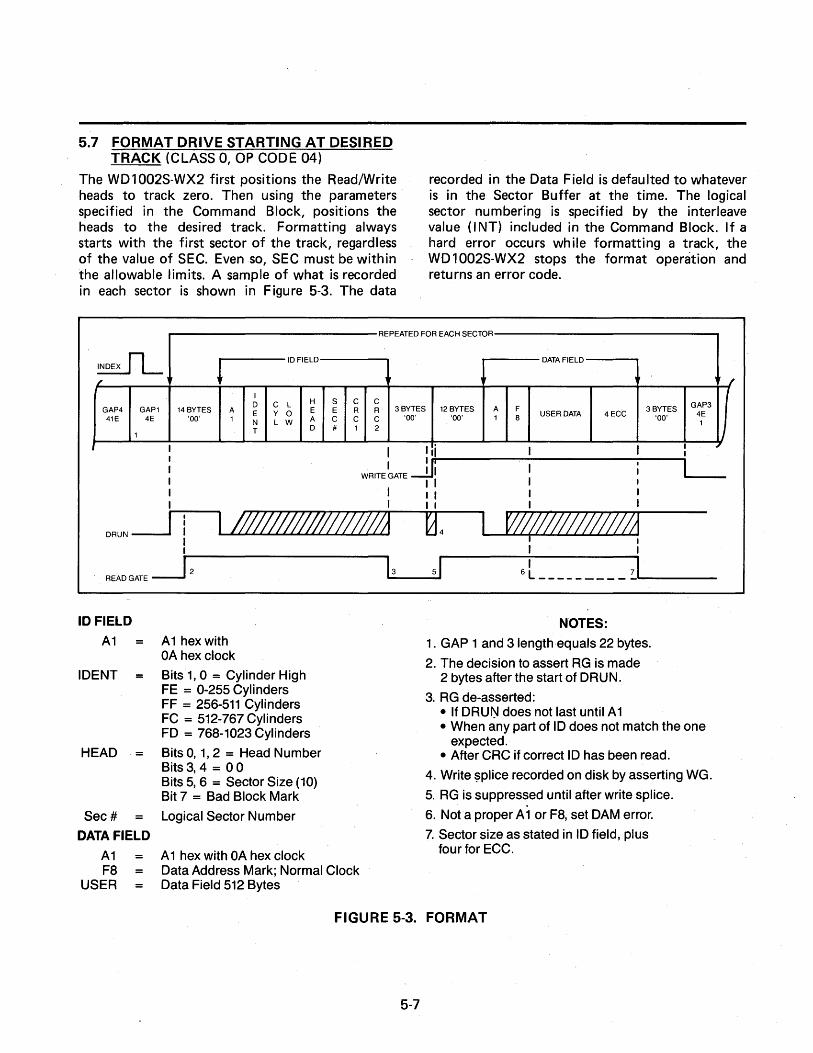
5.7 FORMAT DRIVE STARTING AT DESIRED TRACK (CLASS 0, OP CODE 04)
The WD 1 002S-WX2 first positions the Read/Write heads to track zero. Then using the parameters specified in the Command Block, positions the heads to the desired track. Formatting always starts with the first sector of the track, regardless of the value of SEC. Even so, SEC must be within the allowable limits. A sample of what is recorded in each sector is shown in Figure 5-3. The data
recorded in the Data Field is defaulted to whatever is in the Sector Buffer at the time. The logical sector numbering is specified by the interleave value (I NT) included in the Command Block. If a hard error occurs wh ile formatting a track, the WD 1 002S-WX2 stops the format operation and retu rns an error code.
REPEATED FOR EACH SECTOR
~ ! ID FIELD DATA FIELD
/ 1
I H S C D C L C GAP3
GAP4 GAP1 14 BYTES A E Y 0 E E R R 3 BYTES 12 BYTES A F USER DATA 4ECC
3 BYTES 4E
41E 4E '~O' C C '~O' '~O' 1 8 '~O' 1 N L W A C 1 T D # 1 2
J 1
I I III I I
I !~I'--------~--------------~ WRITE GATE .....!.JI I' 10..--__ I' , I I I
I I I I
DRUN~ I I I I
I !l/l///lff$!I////lj ~4 W/f////////IJl1 I
READGATE~2
10 FIELD
A1
IDENT
HEAD =
Sec #
DATA FIELD
A1 F8 =
USER
A1 hex with OAhexclock
Bits 1,0 = Cylinder High FE = 0-255 Cylinders FF = 256-511 Cylinders FC = 512-767 Cylinders FD = 768-1023 Cylinders
Bits 0, 1, 2 = Head Number Bits 3,4 = 00 Bits 5,6 = Sector Size (10) Bit 7 = Bad Block Mark
Logical Sector Number
A 1 hex with OA hex clock Data Address Mark; Normal Clock Data Field 512 Bytes
,
NOTES:
1. GAP 1 and 3 length equals 22 bytes.
2. The decision to assert RG is made 2 bytes after the start of DRUN.
3. RG de-asserted: • If DRU~ does not last until A 1 • When any part of ID does not match the one
expected. • After CRC if correct 10 has been read.
4. Write ~plice recorded on disk by asserting WG.
5. RG is suppressed until after write splice.
6. Not a proper A 1 or F8, set DAM error.
7. Sector size as stated in ID field, plus four for ECC.
FIGURE 5-3. FORMAT
5-7
5.7.1 POSSIBLE ERROR CODES
02 No Seek Complete 03 Write Fault 04 Disk Not Ready 06 Track Zero Not Found 20 Invalid Command 21 Illegal Sector Address
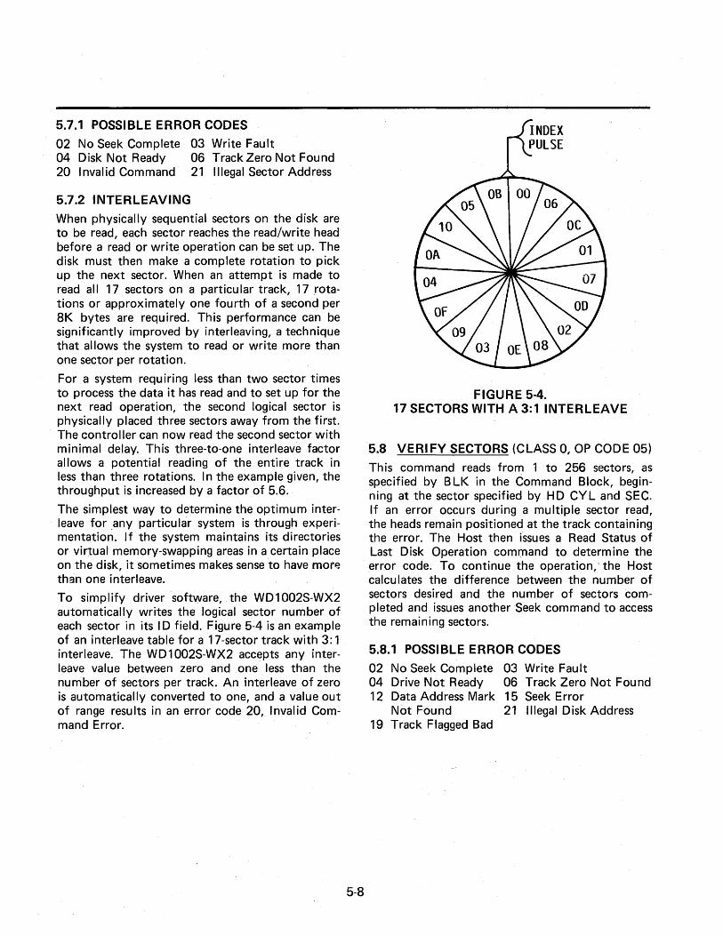
5.7.2 INTERLEAVING
When physically sequential sectors on the disk are to be read, each sector reaches the read/write head before a read or write operation can be set up. The disk must then make a complete rotation to pick up the next sector. When an attempt is made to read all 17 sectors on a particu lar track, 17 rotations or approximately one fourth of a second per 8K bytes are required. This performance can be significantly improved by interleaving, a technique that allows the system to read or write more than one sector per rotation.
For a system requ iring less than two sector times to process the data it has read and to set up for the next read operation, the second logical sector is physically placed three sectors away from the first. The controller can now read the second sector with minimal delay. This three-to-one interleave factor allows a potential reading of the entire track in less than three rotations. I n the example given, the throughput is increased by a factor of 5.6.
The simplest way to determine the optimum interleave for any particular system is through experimentation. If the system maintains its directories or virtual memory-swapping areas in a certain place on the disk, it sometimes makes sense to have more than one interleave.
To simplify driver software, the WD1002S-WX2 automatically writes the logical sector number of each sector in its I D field. Figure 5-4 is an example of an interleave table for a 17-sector track with 3: 1 interleave. The WD 1 002S-WX2 accepts any interleave value between zero and one less than the number of sectors per track. An interleave of zero is automatically converted to one, and a value out of range results in an error code 20, Invalid Command Error.
5-8
FIGURE 5-4. 17 SECTORS WITH A 3:1 INTERLEAVE
5.8 VERIFY SECTORS (CLASS 0, OP CODE 05)
This command reads from 1 to 256 sectors, as specified by B LK in the Command Block, beginning at the sector specified by HD CYL and SEC. If an error occurs during a multiple sector read, the heads remain positioned at the track containing the error. The Host then issues a Read Status of Last Disk Operation command to determine the error code. To continue the operation, the Host calculates the difference between the number of sectors desired and the number of sectors completed and issues another Seek command to access the remaining sectors.
5.8.1 POSSI BlE ERROR CODES
02 No Seek Complete 03 Write Fault 04 Drive Not Ready 06 Track Zero Not Found 12 Data Address Mark 15 Seek Error
Not Found 21 Illegal Disk Address 19 Track Flagged Bad
5.9 FORMAT TRACK (CLASS 0, OP CODE 06)
This command is identical to the Format Drive command, except that only the track specified by the command is formatted. This command can be . used to clear the Bad Track Flag, or reformat individual tracks.
5.10 FORMAT BAD TRACK (CLASS 0, OP CODE 07)
This command is the same as the Format Track command, except that the Bad Track Flag is set in the I D field.
5.11 READ SECTORS (CLASS 0, OP CODE 08)
Th is command reads from 1 to 256 sectors as specified by B LK in the Command Block, beginning at the sector defined by CYL SEC and Head. An uncorrectable error during a mUltiple sector read causes the operation to terminate at the error sector. The Host then issues a Read Status of Last Disk Operation command to determine the type of error. To continue the operation, the Host calculates the difference between the number of sectors desired and the number of sectors completed, then issues another Read command to access the remaining sectors. Error code 06 can only be asserted if the R 1 bit = 0 and the 10 Field has not been read for 10 disk revolutions. This causes the WD1002S-WX2 to recalibrate the heads and seek back to the desired track. If track zero is not detected within 1024 steps, Error Code 06 is set. If R1 = 1 the WD1002S-WX2 aborts the command after a maximum of two disk revolutions, therefore no attempt is made to position the heads to track zero.
5.11.1 POSSIBLE ERROR CODES
02 No Seek Complete 03 04 Drive Not Ready 06 11 Uncorrectable ECC 12
Error 15 Seek Error 18 19 Track Flagged Bad 21
5.12 WRITE SECTORS
Write Fault Track Zero Not Found Data Address Mark Not Found Correctable ECC Error I "egal Sector Address
(CLASS 0, OP CODE OA)
This command writes from 1 to 256 sectors as specified by B LK in the Command Block. The mu Itiple sector transfer scheme works the same as the Read command. Error code 06 can only be asserted if the R 1 bit is 0 and the I D Field has
5-9
not been read for 10 disk revolutions. This causes the WD1002S-WX2 to recalibrate the heads and seek back to the desired track. If track zero is not detected within 1024 steps, Error Code 06 is set. If R1 is 1 the WD1002S-WX2 aborts the command on the first failure to read an I D Field, therefore no attempt to position the heads to track zero is made.
5.12.1 POSSIBLE ERROR CODES
02 No Seek Complete 04 Drive Not Ready 12 Data Address Mark
Not Found 19 Track Flagged Bad
03 Write Fault 06 Track Zero Not Found 15 Seek Error 21 I "egal Disk Address
5.13 SEEK (CLASS 0, OP CODE OB)
This command selects the head and initiates a seek to the track specified by HD and CYL in the Command Block. The SC signal line is not sampled to allow buffered seeks. The cylinder must be in range. The drive must be formatted. Drives employing buffered steps can be issued step pulses at a high speed freeing the WD1002S-WX2 for other. operations. The WD1002S-WX2 does not wait for the drive to complete the seek to return a Command Completion Status. If the return status shows no error, the seek was issued correctly. If there is an error, the seek was not issued. After transferring the status, another command can be issued to either drive. If the WD1002S-WX2 receives a command other than Test Drive Ready for a drive that is still seeking, it asserts BSY and waits for SC to be asserted before executing the command. If the command is a Test Drive Ready, it executes and returns an 08 Drive Still Seeking Error. The time-out for non-buffered seeks. For buffered seeks, the WD 1 015 checks SC before a Read or Write (next command).
The rate at wh ich the Step Pu Ises are issued to the drive is controlled by the SP bits in the Command Block. The drive buffers these pulses and steps at its own rate. Th is allows the WD 1 002S-WX2 to continue about its own business, possibly starting the other drive seeking to a new track, without having to wait for the SC from the first drive. Refer to Table 5.4 for the available stepping rates.
5.13.1 POSSIBLE ERROR CODES
03 Write Fault 04 Drive Not Ready 15 Seek Error

5.14 INITIALIZE DRIVE PARAMETERS (CLASS 0, OP CODE OC)
The WD1002S-WX2 is capable of controlling two drives with different formatted capacity. The B I OS contains four Winchester parameter tables. The configuration jumpers address the proper Winchester parameter table during the B I OS install cycle at power up. Refer to Section 7 for details on these jumper settings. When the Host reads port 322 and discovers a change in drives, it issues this command, followed by the 8-byte block of drive parameters I isted below:
Maximum Number of Cylinders (2 bytes, 1024 max.)
Maximum Number of Heads (1 byte, 8 or 16 heads)
Starting Reduced Write Current Cylinder (2 bytes, 1024 max.)
Starting Write Precompensation Cylinder (2 bytes, 1024 max.)
Maximum ECC Data Burst Length (1 byte, 11 max.)
A typical set of parameters for a 10MB drive is as follows:
306 cylinders RWC at cylinder
153
4 heads Write Precomp at cylinder
153 11-bit burst error length (Western Digital Corp. recommends using a maximum ECC burst length of five or less to ensure optimum integrity of data recovered).
For the exact parameters it is necessary to refer to the specifications for the BIOS in use on the specified board.
5.15 READ ECC BURST ERROR LENGTH (CLASS 0, OP CODE aD)
This command is only valid following a correctable ECC error. It transfers one byte indicating the length of the error. The error length is determined by counting the first through last bit in the error.
5.16 READ SECTOR BUFFER (CLASS 0, OP CODE OE)
This command transfers the 512 bytes of data currently residing in the Sector Buffer to the Host.
5.17 WRITE SECTOR BUFFER (CLASS 0, OP CODE OF)
Th is command writes 512 bytes of data from the Host into the WD 1 002S-WX2 Sector Buffer.
5.18 EXECUTE SECTOR BUFFER DIAGNOSTIC
5-10
(CLASS E, OP CODE 00)
Th is command executes a 9-pass test that uses a 9-byte pattern (0, 1, 2, 4, 8, 10, 20, 40, and 80 ' hex) that is written to the Sector Buffer, then read back. After each successful completion, the whole pattern is shifted one byte position and repeated.
NOTE The WD Format Drive Utility in the WD BIOS executes th is command before physical formatting of the drive. Thus, the data fields are formatted with th is 0, 1, 2, 4, 8, 10, 20, 40, and 80 hex pattern.
5.18.1 POSSIBLE ERROR CODES
30 Data error.
5.19 EXECUTE DRIVE D·IAGNOSTIC (CLASS E, OP CODE 03)
Th is command tests both the drive and the driveto-WD 1 002S-WX2 interface. The WD 1 002S-WX2 sends Recalibrate and Seek commands to the selected drive and reads sector zero of each track verifying both I D and data fields. The WD 1 002SWX2 does not perform any write operations.
5.19.1 POSSIBLE ERROR CODES
02 No Seek Complete 03 Write Fault 04 Drive Not Ready 06 Track Zero Not Found 12 Data Address Mark 15 Seek Error
Not Found
5.20 EXECUTE CONTROLLER DIAGNOSTICS (CLASS E, OP CODE 04)
Regardless of the version of the WD1015 on the WD1002S-WX2, the WD1002S-WX2 executes this command when the Host issues a command code of E4 hex to the CCB. The WD 1 015-14 automatically executes th is command after system Reset (RST on connector P1 B2 asserted), write to port 321 hex, or power-up. The WD 1 015-24 only automatically executes this command when an on-board WD BIOS performs an install sequence after power-up.
Once started, this command continues to run until an error occurs, or the Host selects the WD 1 002SWX2 by writing to port 322. If an error occurs when this command has been started at power up, an error code is output at pins 27, 28, and 29 of the WD 1 015. These are the Head Select 0, 1, and 2 signals and can be monitored at the Drive Control
Connector J 1 pins 14, 18, and 4. The error codes generated under this condition are not the same as those reported by a Read Status command.
1 - WD1010A-05 Error 2 - WD11COO-17 ECC Error 3 - Sector Buffer Error 4 - WD1015 RAM Error 5 - WD1015 ROM Error
5.20.1 WD1010A-05 TEST
A pattern is written to and read from the WD1010A-05's Sector Count and Sector Number Registers.
5.20.2 WD11COO-17 ECC TEST
The WD11 COO-17 is enabled during the read portion of the Sector Buffer Test. After the contents of the Sector Buffer have been read, the ECC not 0 (pin 20) of theWD11COD.-17 is monitored, it should be asserted indicating non-zero Check Bytes. The internal check pattern is then fed back into the chip and pin 20 monitored again. This time it should not be asserted, indicating a Check Byte pattern of zero.
5.20.3 SECTOR BUFFER TEST
The hex pattern ~O, 01, 02, 04, 08, 10, 20, 40, 80 is written throughout the entire Sector Buffer and then read to make sure it is correct. The entire contents of the Sector Buffer is then shifted one byte position and read again. This procedure is repeated nine times verifying that every bit in the Sec~or Buffer can be set and reset.
The WD11 COO-17 is enabled during the read functions to verify the operability of that device.
5.20.4 WD1015 RAM TEST
This tests the 100 bytes of internal RAM in the same manner as the Sector Buffer test.
5.20.5 WD1015 ROM TEST
This test verifies the ability to address and read all 2K bytes of internal ROM, using an add and rotate algorithm to generate a single byte result. This resu It is then compared with the Sumcheck located in the last page of memory.
5.20.6 POSSIBLE ERROR CODES
30 Sector Buffer Error 31 ROM Sumcheck Error 32 ECC Error
5-11
5.21 READ LONG (CLASS E, OP CODE 05)
The Host first performs a normal Write command, writing known data, that produces a predictable ECC character, then performs a Readlong command. This command reads the data from the disk without generating any ECC bytes of its own. Instead it reads the four ECC bytes from the disk, as though reading data, resulting in 512 plus 4 for a total of 516 bytes of data. The Host, knowing what the data and ECC bytes are supposed to be, can now determine whether any errors that have occurred, are a result of a data or ECC failure.
5.21.1 POSSIBLE ERROR CODES
02 No Seek Complete 03 Write Fault 04 Drive Not Ready 06 Track Zero Not Found 12 Data Address Mark 15 Seek Error
Not Found 21 Illegal Disk Address 19 Track Flagged Bad
5.22 WRITE LONG (CLASS E, OP CODE 06)
After performing the Write normal/Readlong routine to determine that the WD1002S-WX2 is able to write data and generate correct ECC bytes, the Host can execute a Writelong and Read normal routine. This verifies the ability of the WD1002SWX2 . to read the data correctly and generate 4-zero E CC bytes or if an error was forced, correct it. The Writelong command does not generate ECC bytes, instead the Host supplies them along with a known data pattern. Then, performing a normal Read command, the Host can determine whether non-zero ECC bytes are caused by a Read failure or ECC generation failure. (This procedure could be performed prior to the Write normal/Readlong).
5.22.1 POSSIBLE ERROR CODES
02 No Seek Complete 03 Write Fault 04 Drive Not Ready 06 Track Zero Not Found 12 Data Address Mark 15 Seek Error
Not Found 21 Illegal Disk Address 19 Track Flagged Bad
SECTION VI THEORY OF OPERATION
6.1 GENERAL
The WD1002S-WX2 Winchester Controller interfaces an I BM PC or .1 BM-compatible PC with a maximum of two Seagate Technology ST506-compatible disk drives. Western Digital bases the WD1002S-WX2 architecture on the WD1010A-05 Winchester Disk Controller, WD1015-14 (WD1015-24) Buffer Manager Control Processor, WD 11 COO-17 Logic Array, WD 1 OC20 Winchester Data Separator and Write Precompensation Device, and BIOS ROM. Therefore, this theory of operation focuses upon these devices. Figure 6-1 is a functional block diagram of the WD1002S-WX2.
6.2 BUSES
This section describes the five buses used by the WD 1 002S-WX2. Two of the buses are extensions of the Host data and address buses. The other three buses are internal to the WD 1 002S-WX2. All buses transm it either addresses, commands, data or status information.
6.2.1 HOST INTERFACE ADDRESS BUS AO THROUGH A19
The Host uses this bus during programmed I/O to address the eight I/O ports 320 hexidecimal through 327 hexidecimal. The Host also addresses the BIOS ROM with address CBOOO-CBFFF on this bus.
6.2.2 HOST INTERFACE DATA/COMMAND BUS DO THROUGH 07
This is a bi-directional data bus linking the WD 1 002S-WX2 to the Host. It ·is used for the transm ittal of data between the Host and Sector Buffer, the Command Control Block (CCB) to the WD 1 015, and the drive configuration and status to the Host.
6-1
6.2.3 WD1002S-WX2 INTRABOARDCOMMAND/ STATUS BUS BOO THROUGH BD7
This is a read only bus connecting the BIOS ROM to DO through 07, through a bus drivers controlled by ROMEN. When the Host requests information from the B lOS, the Host addresses the B I OS and enables the bus drivers. The information passes from BOO - BD7 to DO - 07. The information transfer between the B I OS and Host follows standard bus protocol.
6.2.4 WD1002S-WX2 INTRABOARDCOMMAND/ STATUS BUS ADO THROUGH AD7
This is a bi-directional bus linking the WD1015, WD1010A-05, WD11COO-17, and Sector Buffer. Data, commands, control information and status all pass through this bus. This bus is linked to the DO through 07 bus by the WD11COO-17.
6.2.5 WD1002S-WX2 INTRABOARD ADDRESS· BUS RAO THROUGH RA10
This bus addresses the Sector BufferandWD1010A-05 Task File, as well as signaling the WD1010A-05 that the end of the data field has been reached and the ECC is starting. The Task File address is preset into the WD 11 COO-17 Sector Address Counter which in turn places it on the RAO through RA10 bus. The Task File address is eight bits long.

. Pl A ,....;- - ~
~ ~ DATA BUS 0~ 0 AO-A12 BOO-B07
DRIVERS R H C t---
~"r .~ G)~ I o 0 r BIOS r 00-07 HSELO-HSEL3*
~ V
S N ROM f-- 0~ r E
T N ROMEN*
r WR OSELO* ~
I E ..... C
1 N C AZ~A7 ,A9,A13-A19 ~o~ig:s ~
T T E 0 DECODER R R MEMR llAllO F 1 i.....--A C E 00-07
AEN ... '--Pl-B - ~ H C o 0 S N T N ID\CK3
E TOR I C N T TOW T 0 E R RESET R F OR03 A
IRQ5(IRQ2)* C E ~
'--
~ o 0 RMFM R A I T V A E
~ DELAY LINE
~ ~
Jl I . AOO-A07 RG*
- r WO
0 jjfWY mIT R SC LATE I V TNDEX WINT 0 E
TKOOO W010l0A-05 ROATA C
_L.cv WINCHESTER 0 OISK RCLK N CONTROLLER ORUN T WF
R RilC* WCLK 0 "-L WG mom
0 _ RA10
RA9
RA8
*REFER TO SECTION 7 FOR DETAILED INFORMATION ON JUMPER LOCATIONS AND FUNCTIONS.
0 RO OSELl N ...-
c/o STEP T
~ R
I/O 0 W01015 L .. Z. .A
csm BUFFER MANAGER \I' 00-07 IREQ CONTROL
AEN r REQ PROCESSOR
liTISY _
I ~ ECC NOT 0
CONFI GURA TI ON OPO-OP3 OPO-OP3 L/S/OIR/WPC
JUMPERS* I r
J\ ~
1lACIcr ~O_Ar lOR _"
TOW WOll00-17 LOGIC
RESET ARRAY AOO-A07 I ORQ3
C IRQ5(IRQ2)*
~ -V
~
RliM'iiR ~ SECTOR . BUFFER
TEARLY WCLK ® RAO-RA9 TNOMINAL
'" co W010C20 c( c( TLATE '" '" OLYOR
WCLK
ORUN
RCLK ~
~ ~
FIGURE 6-2. WD1002S-WX2 DETAILED BLOCK DIAGRAM
6.3 BUS PROTOCOL
The Host and WD 1 002S:WX2 protocol consists of the following bus phases:
Select Command Data Completion
Normal execution occurs in the order listed above.
6-2
Depending upon the type of command being executed, the Data phase does not always occur. Also, depending upon the type of errors detected by the WD1015 or WD1010A-05, an immediate skip to the Completion phase can occur. Execution of the Completion phase always occurs regardless of the command or error.

6.3.1 SELECTION PHASE
The Host selects th is phase to start execution of a command by the WD1002S-WX2. The WDllCOO-17 asserts BUSY to acknowledge selection of the WD1002S-WX2. The Host can sample BUSY by reading port 321 hex. For power-up and at the end of every command, the WD 1 002S-WX2 asserts the hardware status bits required for proper handshake as follows:
BUSY C (C/D) T (T/O) REO
When the Host reads the WD 1 002S-WX2 hardware status the WDllCOO-17 complements BUSY and C/D and drives these signals onto the Host data bus. Sections 5.2.1 through 5.2.4 describe the I/O, ports in detail.
6.3.2 COMMAND PHASE
Following the Selection phase, the Host sends the six byte Command Control Block (CCB). Transfer of the require assertion of the hardware status bits BUSY, C (C/D), T (T/O), and REO. The WDllCOO~ 17 sends the CCB to page 0 of the Sector Buffer. The WD 1 015 retrieves the CCB from the Sector Buffer to execute the command. Once th is phase is entered, the only way the Host can abort command execution is by asserting RESET. The Host can reissue commands when the WD 1 002S-WX2 de-asserts BUSY. Section 5.3 describes the cca format.
6.3.3 DATA PHASE
After decoding a command and checking for any illegal parameters, the WD1015 sets up the Host for the Data phase depending upon whether the WD 1 015 needs the data first to execute the command. Otherwise, the Data phase is entered, after the command is executed by the WD 1 015, as in the case of a Read Command. Assertion of 0 (C/D) defines the Data phase. The state of the I/O signal and the command determines the direction of the data transfer. Assertion of I (I/O) indicates data input to the Host. Assertion of 0 (I/O) indicates data output from the Host.
6-3
6.3.3.1 Programmed I/O Data Transfer The Host usually transfers commands and data in programmed I/O mode except disk data transfers. Disk data transfers can be either programmed I/O or DMA. To the WD 1002S-WX2, both methods of data transfer are identical except for the generation of the handshake signals by the WD 11 COO-17. The WDllCOO-17 does not generate the DR03 signal in programmed I/O mode. lOR and lOW transfer the data when the W D 1 015 asserts the hardware status bits.
The WD 1 002S-WX2 I/O ports reside in Host memory address locations 320 hex through 323 hex. (The WD 1 002S-WX2 allows jumper selection of the I/O port addresses. Refer to Section 7 for further information.) All WD 1 002S-WX2 port accesses are made in programmed I/O mode. Address enable (AEN) indicates Host control over the buses and connects the I/O channel to the WD 1 002S-WX2. AO through AS address the Host memory locations. AO and A 1 select one of the four ports. lOR and lOW select the port function. Depending upon the addressed port function, the Host bus may not be used. Section 5.2 describes the I/O ports and their functions. Section 4 describes interface timing for programmed I/O data transfers.
6.3.3.2 DMA Data Transfer The Host must configure the WD1002S-WX2 for DMA mode before transfer data between the Sector Buffer and Host. The Host writes to port 323 hex to enable DMA mode prior to issuing a command. With DMA eanbled, no access of port 320 is required to transfer data. The Host can then sense D R03 at the start of a byte transfer. Assertion of DACK3 by the Host causes the WD 11 COO-17 to de-assert D R03. Data transfer between the Sector Buffer and Host is then controlled by the Host using lOW and iDA signals as in programmed I/O mode. When DACK3 is de-asserted, D R03 is asserted by the WD 11 COO-17. This process repeats until all the data is transferred. De-assertion of REO signals the end of the DMA transfer. Section 4 describes interface timing for DMA data transfers.

6.3.4 COMPLETION PHASE
The Host senses the Completion phase by sampling I R05 (I R02 is a jumper selectable option. Refer to Section 7.) or by polling the BUSY signal. I R05 is available as a port 321 status bit. The Host totally controls I R05 by writing to port 323. The WD11 COO-17 generates I R05 when the Host issues the write to port 323. The Host must disable interrupts before reading the Command Completion byte from the WD1002S-WX2. If the Host does not disable the WD 1 002S-WX2 interrupts, then the WD 1 002S-WX2 continuously interrupts the Host. The completion code can be read by the Host when the WD11COO-17 asserts the following hardware status signals:
BUSY C (C/O) I (I/O) REO
A completion code of zero indicates no error occured. A non-zero value indicates occurrence of an error during command execution. The Host can obtain additional information about the error by executing a Read Status Command. In this case, the Data phase is implemented at command completion by the WD 1 002S-WX2.
The WD 1 015 makes the command completion byte available to the Host at port 320 after command completion. This byte contains the drive number of the drive that completion status is val id and an error bit. Section 5.6 describes the format of the command completion byte.
6.4 DEVICE ADDRESS DECODER
The Device Address Deocder generates ROM ENABLE (ROMEN) and DEVICE ADDRESS CODE (DADD). ROMEN allows the Host to address the B lOS ROM and enables the ROM Data Bus Drivers to place the B I OS ROM information on the Host Interface Data/Command Bus. ROMEN is derived from a valid BIOS address and MEMR. DADD is asserted when address 320 or 324 is present on the address bus.
6.5 BIOS ROM
The B I OS ROM contains firmware driver routines for Winchester disk control. These routines, when installed, reside in Host memory space C8000 hex through C8FFF hex. The BIOS routines are only entered via software interrupts. If your Host
6-4
operating system is designed to supply the BIOS ROM information, then the WD1002S-WX2 BIOS ROM is not required to operate the controller.
6.6 CONFIGURATION JUMPERS
These jumpers configure the WD1002S-WX2 for different disk drive capacities. Pull-up resistors internal to the WD 11 COO-17 normally tie the OPTION 0 through 3 (OPO through OP3) signals to +5V. Installation of a jumper connects the signal to ground. Section 7 describes the Configuration Jumper location and settings for disk drive capacities.
6.7 WD11COO-17 LOGIC ARRAY
The WD11 COO-17 Logic Array incorporates several functions in a single package. Implementation of these functions occurs by combining random logic and specialized circuits. The WD11COO-17 contains the following circuits:
Status ports Read and write ports Sector Buffer RAM addressing and control ECC Reset timing
The WD 11 COO-17 connects directly to the mu Itiplexed address/data bus, ADO - AD7.
6.7.1 STATUS, READ, AND WRITE PORTS
Section 5.2 describes these ports' functions. Section 6.3 describes the operation of these ports.
6.7.2 SECTOR BUFFER RAM ADDRESSING AND CONTROL
A counter in the WD11COO-17 generates RAM ADDRESS 0 through 9 (RAO through RA9). The upper three address bits (RA7, RA8, and RAg) are resettable by the WD 1 015. This allows the WD 1015 to address a range of 8 pages with 256 bytes in each page. The address of any byte within a page can be set by the WD1015 by generating dummy RAM accesses to increment the address counters to the proper address.
I n addition to addressing the Sector Buffer, the upper three counter bits (RA8, RAg, and RA 10) are used to address the WD1010A-05 Task File when the Sector Buffer is not being used. A Sector Buffer access ends when the Sector Buffer is empty or full. Therefore, the WD11COO-17 asserts RA10.

Assertion of RA 10 causes de-assertion of D RQ3. This informs the Host that the Sector Buffer is either empty or full, signals the end of the data field, and indicates the start of the ECC field to the WD11 COO-17 ECC logic.
Assertion of RA3 when the Command bus phase ends indicates to the WD 1015 placement of the CCB in the Sector Buffer.
6.7.3 ECC CIRCUITRY
During a write operation, the WD 1 01 OA-05 receives the data from the Sector Buffer. The WD 11 COO-17 generates and appends the four byte ECC to the data stream. Proper placement of the ECC requires determ ination of the end of the data stream. Assertion of RA10 by the WD11COO-17 address counter indicates RAM overflow and the end of the data stream. After writing the ECC to the disk, the WD11 COO-17 ECC circuitry supplies all zero bytes to the ADO through AD7 bus as long as ECC fu nction is selected.
During a read operation, the ECC circuitry recomputes the ECC. Comparison of the previously written ECC and computed ECC occurs at the end of the data stream. (Assertion of RA 10 indicates end of the data stream.) The ECC circuitry records the resu It of the comparison. Any additional writes to the Sector Buffer are ignored. If the result of the comparison is non-zero, then the WD11 COO-17 asserts ECC NOT 0 signal. Assertion of ECC NOT 0 enables the WD 1 015 to attempt error correction.
For diagnostic purposes, during Writelong and Readlong commands the ECC generation and checking is disabled. A Writelong command causes the WD11COO-17 to accept any four bytes from the Host, and stores the bytes internally. These bytes are written to the disk unaltered. A Readlong command causes the WD 11 COO-17 to accept the four bytes written on the disk. These bytes are passed to the Host unaltered. This allows the Host to induce errors anywhere in the data stream and check for predictable results. Sections 5.21 and 5.22 describe these commands.
During sector reads and writes, CRe error detection capability is used for the I.D. fields. The data field on a hard disk uses error correction for a single burst up to 11 bits in error. The bit correction span is user programmable. Use the 11 bit correction span sparingly or only for diagnostic purposes. Eleven bit error correction spans signifi-
6-5
cantly reduce error detection for multiple error bursts. A five bit correction span is adequate for most applications.
6.7.4 RESET TIMING CIRCUITRY
For a reset, the WD 1 002S-WX2 executes a powerup sequence to setup internal parameters and initializes the on-board circuitry properly. The WD1002S-WX2 design requires a minimum warm reset pulse width of 15J,Jsec. The Reset Timing circuitry provides a warm reset pulse of 1.35 msec. For a cold start, the minimum reset required pulse· width is 10 msec. The Reset Timing circuitry provides a cold reset pulse of 128 msec.
To detect any power up diagnostic failures, the Host should issue an Execute Controller Diagnostic command if the WD1002S-WX2 DOES NOT use either a WD1015-14 or a WD 810S. The WD1015-14 automatically performs an Execute Controller Diagnostic command after power-up or a software reset. A WD 8 I OS issues an Execute Controller Diagnostic command as part of the install sequence regardless of the version of the WD 1 015 on-board.
6.8 WD1015 BUFFER MANAGER CONTROL PROCESSOR
The WD 1 015 is a self contained CPU designed to receive commands from the Host. Firmware in the WD1015 translates the Host command format into the WD1010A-05 format. The WD1015 controls any programmable retries and data error correction.
There are two versions of the WD1015 for the WD1002S-WX2. The WD1015-14 supports up to eight heads. The WD1015-14 uses the REDUCED WRITE CURRENT (RWC) signal. The WD1015-24 supports up to 16 heads. The WD1015-24 uses the RWC pin on J1 as HEAD SELECT 3 (HSEL3). The acronym WD1015 refers to both- versions. When a specific reference is made to a specific version, the appropriate acronym is used.
The WD1015 controls the transfer of information within the WD1002S-WX2 and maintains the necessary copies of the WD1010A-05 Task Files. The WD1015 accesses the CCB in the Sector Buffer. Prior to the command being issued to the WD1010A-05 by the WD1015, the drive and head select information is set in a port latch for the drive interface (DSE LO, DSE L 1, and HSE LO through HSE L3). The heads are stepped, if required, by the STEP signal and positioned over the

desired cylinder. The CCB is translated and issued to the WD1010A-05, after observing the required protocol. At the end of command execution, the WD1010A-05 asserts WINT. The WD1015 polls WINT.
The WD1015 controls multiple sector transfers without the Host reissu ing the command. The WD1015 breaks all multiple sector transfers into a series of single sector commands to the WD1010A-05. The WD1015 provides head changes and steps as required between WD1010A-05 commands until the block count is satisfied. There can be many WD 1 01 OA-05 interrupts (W I NT) for one Host command. However, the WD 1 015 enables the WD11COO-17 to send only one interrupt to the Host at the end of the transfer.
6.8.1 EXCEPTION HANDLING
No commands can be executed by the WD 1 01 OA-05 with D RDY de-asserted, SC de-asserted, or WF asserted. I n these cases, the WD 1 015 aborts the issued comr11and. No attempts are made to recover from these conditions.
Before any data transfer can take place, the WD1010A-05 attempts to read the I.D. field of the logical block address specified. If any errors are detected in this process, the WD1010A-05 attempts to read the I.D. field until two index pu Ises are detected. If the I. D. field can not be read, the WD1015 reissues the command once each disk revolution for ten disk revolutions to recover from the error. If this is unsuccessful, the WD 1 015 performs an Autorestore. The Autorestore recalibrates the selected logical unit and performs a re-seek to the logical block address specified. The WD1010A-05 attempts to read the I.D. field once each disk revolution for ten disk revolutions. If the error is unrecoverable, the operation is terminated. The error reported is the last error encountered assuming that the same error is responsible for an; attempted retries.
A similar operation is performed on all missing Data Address Marks during a read operation. If the I. D. field can be read correctly, data transfer between the Host and WD1010A-05 can take place. For a write operation, the location of the desired I.D. field is all that is required to write data to the disk from the Sector Buffer. Mu Itiple sector transfers are broken into single sector transfers as described in Section 6.B. For a read operation, the data field is corrected, if possible, before being transferred to the Host.
6-6
The WD 1 015 controls the operation of the WD11COO-17 ECC circuitry. During the transfer of data from the Sector Buffer to the disk, the WD11COO-17 computes a four byte ECC that is appended to the end of the data transferred to . the WD1010A-05 and recorded on the disk. During data transfers from the WD 1 01 OA-05 to the Sector Buffer, the WD11 COO-17 uses the ECC circuitry to validate the data. If data is corrputed, the WD1015 performs retries and correction. A maximum of eight retries are attempted if two consecutive syndromes do not match. Correction is attempted only when two consecutive syndromes match. If the error ·is uncorrectable the operation is terminated. '
All exception handling results in a loss of at least one disk revolution.
6.9 SECTOR BUFFER
The Sector Buffer consists of a 2KB by 8 bit RAM that is used to hold data or the CCB. Only the lower 1 KB of the RAM is actually used. Therefore, the terms upper and lower in the succeeding paragraph are relative to the lower 1 KB of the RAM.
The lower half of the RAM is used mainly for the CCB, status and error information, and storage for the ECC bytes. The eight bytes of drive characteristics from the Host during an Initialize Drive Parameters command are also stored in page zero of the RAM. The sector data is stored in the upper half of the RAM. The Sector Buffer also holds the information to be recorded on the disk during a Format command in exactly the same way as a sector of data written to the disk.
6.10 WD1010A-05 WINCHESTER DISK CONTROLLER
The WD1010A-05 is a single chip device designed for use with Seagate Technology ST506 and other compatible disk drives. All disk commands are started by the WD 1 015 after the CCB has been read and properly translated. The primary purpose of the WD1010A-05 is to control data (this includes data separation for Read Data) transfer between the disk and the Sector Buffer after the WD1015 has positioned the selected head over the desired track. The WD1010A-05 can position the disk heads, but this capability is not used in the design because the desired step rates are not supported by the WD1010A-05. Refer to the WD1010-05 data sheet in the Western Digital Storage Management Products Handbook for further details on the WD 1 01 OA-05.
6.11 WD10C20
The WD10C20 interfaces the disk drive to the other circuitry on the WD1002S-WX2. The WD10C20 contains two major circuits. These two circuits are the Write Precompensation circuitry and data synchronization.
6.11.1 CLOCK GENERATOR
A 10 MHz fundamental frequency crystal is required by the WD10C20. The crystal frequency is used as a reference clock and then divided by two for a WRITE CLOCK (WCLK) which is used to produce M F M write data for the disk. These Clock sources are provided by the WD10C20.
The WD 1015 uses the 5 MHz WCLK, provided by the WD10C20, giving an instruction cycle time of 3.0J,Jsec. Most instructions execute in two cycles or 6.0usec.
6.11.2 WRITE PRECOMPENSATION CIRCUIT
The generation of M F M Write Data takes place in the WD1010A-05. The WD1010A-05 accepts a byte of data and a WCLK to internally produce M F M data. The M F M data is now totally compatible with the required format for transmission to the disk via I ine drivers with one exception. Due to decreasing radius on the physical surface of the disk, the inside tracks have less circumference and therefore exhibit an increase in recording flux density over the outside tracks. This increase in flux density aggravates a problem known as dynamic bit shift.
Dynamic bit shift comes about as a result of one ·bit on the disk (a flux reversal) influencing an adjacent bit. The result is to shift the leading edge of both bits closer together or further apart than originally recorded. The net result is that enough jitter is added to the data recorded on the inside tracks to make them harder to recover without error.
Write precompensation is used to reduce the effect of dynamic bit shift on the recorded data. It is a method of predicting which direction a particular bit is shifted and intentionally writing that bit out of position in the opposite direction from the expected shift. This is performed by examining two data bits: the last one written and the present one to be written to the disk. A comparison of these bits produces one of three signals: EAR L Y, NOMINAL, or LATE. These signals are used with a delay line (intervals of 12nsec) to cause the leading
6-7
edge of the data or clock bit to be written EAR L Y, LATE, or on time (NOMINAL).
The WD1015 enables or disables the generation of these write precompensation signals by controll ing the LS signal. Assertion of LS enables write precompensation. De-assertion of LS disables write precompensation and the NOMINAL output is asserted.
The WD10C20 internal logic performs the write precompensation. The MFM write pulses are applied to internal logic. The WM FM output depends upon the state of the three write precompensation signals. From here, the data is converted to a differential form and then transmitted to the disk drive.
6.11.3 DATA SEPARATOR
Data is recorded on the disks using MFM techniques. This technique requires clock bits to be recorded only when two successive data bits are missing in the serial data stream. In other words, if two successive data bits are zeroes, then a clock pulse is generated. A logical one data bit is recorded as a pulse and a logical zero is recorded as not pu Ise. The fact that clock bits are not recorded with every data bit cell requires circuitry that can remain in synchronization with data during the absence of clock bits. Synchronous decoding of MFM data streams requires the decoder circuitry to synthesize clock bit timing when clocks are missing and synchronize to clock bits when they are present. This is accomplished by using a phase locked oscillator employing an error amplifier and filter to synchronize with and hold a specific phase relationship to the data and clock bits in the data stream. The phase lock occurs at the 'crystal frequency, wh ich in turn is used to synthesize a clock called RCLK with a frequency one half of the crystal frequency. This synthesized clock is used to separate data bits from clock bits by the external logic for deserialization into bytes.
Refer to the WD10C20 Data Sheet for further details.

SECTION VII INSTALLATION
7.1 HARDWARE AND SOFTWARE INSTALLATION
This section briefly describes installation of the WD 1002S-WX2 in an I BM PC or IBM-compatible computer.
1. Ensure system power is off. 2. Insert WD1002S-WX2 in computer chassis and
connect drive cables. (J 1 = control cable, J2 = drive 0 cable, J3 = drive 1 cable.)
3. Powerupthesy~em.
4. Insert IBM PCDOS 2.0 or IBM PCDOS 2.1 diskette.
CAUTION Performing steps 5 through 9 destroys any data presently on the disk.
5. Load DEBUG utility by typing IIdebug" and E NTE R after the DOS prompt.
6. Initiate the WX2FMT (format) program by typing the following command line: -g=c800:5
7. Press lIy" to begin formatting drive 0 (logical drive C).
8. To format drive 1 or second drive in a daisy chain, reload DEBUG utility. Type "RAX" and E NTE R. Prompt returns II AX 0000". Type
110103", ENTE R which defines relative drive number and interleave factor (01 = relative drive number; 03 = interleave factor). Type "G=C800:5", ENTER, and type "y" to begin formatting drive 1 (logical drive D).
9. Run standard DOS utilities, FDISK and FORMAT.
7.2 JUMPER INSTALLATION AND LOCATIONS
The WD 1 002S-WX2 is configured for the standard IBM PCXT with jumper plugs installed at W3, W4, and W6. No jumpers are required at W5 and W7. To change the configuration, a jumper plug can be installed in the appropriate block. Installation of jumpers on W5 and W7 requires carefully cutting an etch and placing a jumper· plug onto the Jumpered position. To restore the standard setting, move the jumper plug to the Standard position. Table 7-1 describes these jumpers and options. Table 7-2 describes the drive configuration jumpers and an INTERRUPT REQUEST (IRQ) jumper in SW1. Figure 7-1 illustrates the locations of W1 through W7 and SW1.
TABLE 7-1. JUMPER SELECTABLE OPTIONS (¥V1 THROUGH W5)
JUMPER FUNCTION PIN DESCRIPTION
W1, W2 For Western Digital Manufacturing use only.
W3 Standard: 1-2 Closed by etch or jumper. Enables BIOS ROM. Jumpered: 1-2 Open. Disables BIOS ROM.
W4 Standard: 2-3 Selects primary port 320 hex. Jumpered: 1-2 Selects secondary port 324 hex. Requires custom BIOS.
NOTE The WD1002S-WX2 provides two sets of I/O ports. The primary port addresses are 320 through 323 hex. The secondary port addresses are 324 through 327 hex. However, secondary ports on the WD1002S-WX2 are NOT supported by any version DOS.
W5 Standard: 1-2 Selects 2732 or 2764 B I OS R OM size. Jumpered: 2-3 Selects 2716 BIOS ROM size. W5 pin 1-2 etch must be cut.
W6 Standard; 2-3 8 head configuration, RWC used. Jumpered: 1-2 16 head configuration, RWC not used, requires custom BIOS ROM and
WD1015-24.
W7 Standard: 1-2 Selects I RQ5. Jumpered: 2-3 Selects I RQ2. SW1 position 8 must also be jumpered (closed) and W7
pin 1-2 etch must be cut.
7-1
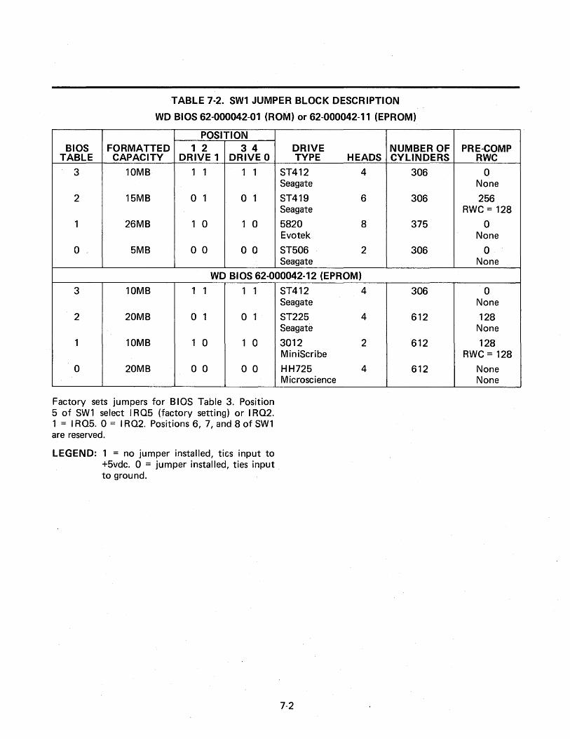
TABLE 7-2. SW1 JUMPER BLOCK DESCRIPTION
WD BIOS 62-000042-01 (ROM) or 62-000042-11 (EPROM)
POSITION BIOS FORMATTED 1 2 3 4 DRIVE
TABLE CAPACITY DRIVE 1 DRIVE 0 TYPE HEADS
3 10MB 1 1 1 1 ST412 4 Seagate
2 15MB 0 1 0 1 ST419 6 Seagate
1 26MB 1 0 1 0 5820 8 Evotek
0 5MB o 0 o 0 ST506 2 Seagate
WD BIOS 62-000042-12 (EPROM)
3 10MB 1 1 1 1
2 20MB 0 1 0 1
1 10MB 1 0 1 0
0 20MB o 0 o 0
Factory sets jumpers for BIOS Table 3. Position 5 of SW1 select I R05 (factory setting) or I R02. 1 = I R05. 0 = I R02. Positions 6, 7, and 8 of SW1 are reserved.
LEGEND: 1 = no jumper installed, tics input to +5vdc. 0 = jumper installed, ties input to ground.
ST412 4 Seagate
ST225 4 Seagate
3012 2 MiniScribe
HH725 4 Microscience
7-2
NUMBER OF CYLINDERS
306
306
375
306
306
612
612
612
PRE-COMP RWC
0 None
256 RWe = 128
0 None
0 None
0 None
128 None
128 RWe = 128
None None
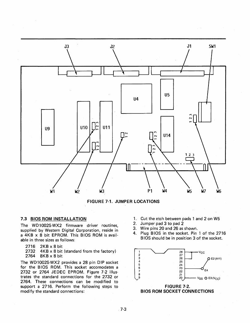
J3 J2 J1 SW1
U5 U4
1""1
U9 U10 N U11 ~
W2 W3 P1 W4 W5 W7 W6
FIGURE 7-1. JUMPER LOCATIONS
7.3 BIOS ROM INSTALLATION
The WD1002S-WX2 firmware driver routines, supplied by Western Digital Corporation, reside in a 4KB x 8 bit EPROM. This B IDS ROM is available in three sizes as follows:
2716 2KB x 8 bit 2732 4KB x 8 bit (standard from the factory) 2764 8KB x 8 bit
The WD1002S-WX2 provides a 28 pin DIP socket for the B IDS ROM. This socket accomodates a 2732 or 2764 JEDEC EPROM. Figure 7-2 illustrates the standard connections for the 2732 or 2764. These connections can be modified to support a 2716. Perform the following steps to modify the standard connections:
.7-3
1. Cut the etch between pads 1 and 2 on W5 2. Jumper pad 3 to pad 2 3. Wire pins 20 and 26 as shown. 4. Plug BIOS in the socket. Pin 1 of the 2716
BIOS should be in position 3 of the socket.
1 2 3 4 5 6 7 8 9
28 Vcc 27 26 E2(A11) 25 24 23 ~--n 22 21 20 Vss 0 E3 (VCe>
FIGURE 7-2. BIOS ROM SOCKET CONNECTIONS

WESTERN DIGITAL CORPORA TION
2445 McCabe Way Irvine, California 92714 (714) 863-0102 TWX 91Cl-595-1139