ns7520 data sheet - digi internationalftp1.digi.com/support/documentation/90000303_e.pdfns7520...
TRANSCRIPT
NS7520 Data Sheet
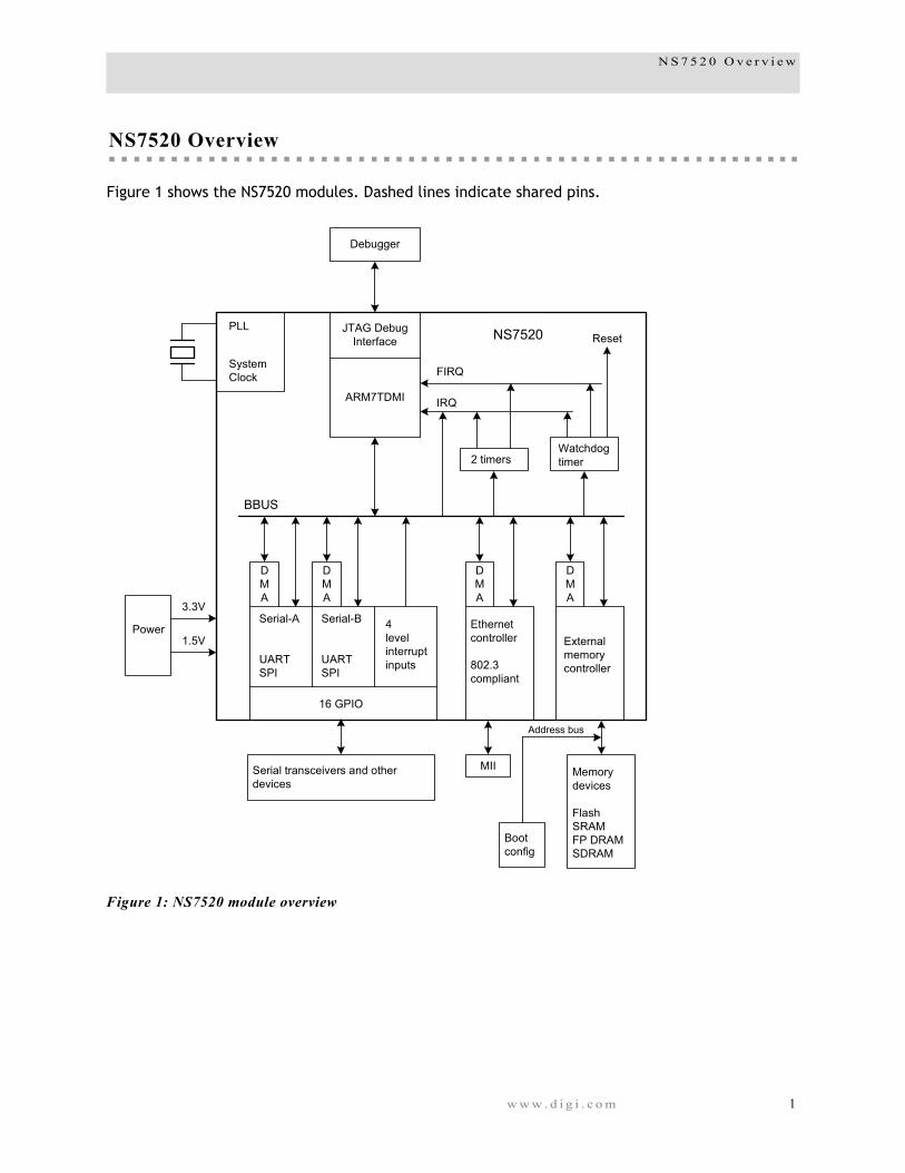
The Digi NS7520 is a high-performance, highly integrated, 32-bit system-on-a chip ASIC designed for use in intelligent networked devices and Internet appliances. The NS7520 is based on the standard architecture in the NET+ARM™ family of devices.
The NS7520 can support most any networking scenario, and includes a 10/100 BaseT Ethernet MAC and two independent serial ports (each of which can run in UART or SPI mode).
The CPU is an ARM7TDMI 32-bit RISC processor core with a rich complement of support peripherals and memory controllers for various types of memory (including Flash, SDRAM, EEPROM, and others), programmable timers, a 13-channel DMA controller, an external bus expansion module, and 16 general-purpose input/output (GPIO) pins.
NET+ARM is the hardware foundation for the NET+Works™ family of integrated hardware and software solutions for device networking. These comprehensive platforms include drivers, popular operating systems, networking software, development tools, APIs, and complete development boards.

Contents
NS7520 Overview........................................................................... 1Key Features................................................................................ 2Operating frequency ...................................................................... 3Packaging and pinout ..................................................................... 4Pinout detail tables ....................................................................... 6
System Bus interface............................................................. 6Chip select controller...........................................................10Ethernet interface MAC.........................................................11“No connect” pins ...............................................................13General Purpose I/O ............................................................13System clock and reset .........................................................15System mode (test support) ...................................................16JTAG test .........................................................................16Power supply .....................................................................17
NS7520 modules...........................................................................18CPU module ......................................................................18GEN module ......................................................................18System (SYS) module............................................................18BBus module......................................................................19Memory module (MEM)..........................................................19DMA controller ...................................................................19Ethernet controller..............................................................19Serial controller .................................................................21
NS7520 bootstrap initialization .........................................................22JTAG...............................................................................22ARM Debug........................................................................22
DC characteristics and other operating specifications..............................23Absolute maximum ratings.....................................................24Pad pullup and pulldown characteristics ....................................24
AC characteristics ........................................................................25AC electrical specifications ....................................................25
Oscillator Characteristics................................................................27Timing Diagrams ..........................................................................28
Timing_Specifications...........................................................28Reset_timing .....................................................................29SRAM timing ......................................................................30SDRAM timing ....................................................................40FP DRAM timing ..................................................................46Ethernet timing ..................................................................53JTAG timing ......................................................................55External DMA timing ............................................................57Serial internal/external timing................................................59GPIO timing.......................................................................61
i i i

N S 7 5 2 0 O v e r v i e w
NS7520 Overview
Figure 1 shows the NS7520 modules. Dashed lines indicate shared pins.
Figure 1: NS7520 module overview
Debugger
PLL
SystemClock
JTAG DebugInterface
ARM7TDMI
FIRQ
IRQ
2 timersWatchdogtimer
Power
3.3V
1.5V
BBUS
DMA
DMA
DMA
DMA
Serial-A
UARTSPI
Serial-B
UARTSPI
4levelinterruptinputs
16 GPIO
Ethernetcontroller
802.3compliant
Externalmemorycontroller
NS7520 Reset
Address bus
Serial transceivers and otherdevices
MII Memorydevices
FlashSRAMFP DRAMSDRAM
Bootconfig
w w w . d i g i . c o m 1
K e y F e a t u r e s
Key Features
This table lists the key features of the NS7520.
CPU core Integrated 10/100 Ethernet MAC
ARM7TDMI 32-bit RISC processor 32-bit internal bus 32-bit ARM and 16-bit Thumb mode 15 general purpose 32-bit registers 32-bit program counter (PC) and status register Five supervisor modes, one user mode
10/100 Mbps MII-based PHY interface 10 Mbps ENDEC interface TP-PMD and fiber-PMD device support Full-duplex and half-duplex modes Optional 4B/5B coding Station, broadcast, and multicast address detection 512-byte transmit FIFO, 2 Kbyte receive FIFO Intelligent receive-side buffer selection
13-Channel DMA controller Programmable Timers
Two channels dedicated to Ethernet transmit and receive Four channels dedicated to two serial modules’ transmit
and receive Four channels for external peripherals. Only two
channels — either 3 and 5 or 4 and 6 — can be configured at one time. Three channels available for memory-to-memory
transfers Flexible buffer management
Two independent timers (2μs–20.7 hours) Watchdog timer (interrupt or reset on expiration) Programmable bus monitor or timer
General purpose I/O pins Operating frequency
16 programmable GPIO interface pins 4 pins programmable with level-sensitive interrupt
36, 46, or 55 MHz internal clock operation from 18.432 MHz crystal fMAX = 36, 46, or 55 (grade–dependent) System clock source by external quartz crystal or crystal
oscillator, or clock signal Programmable PLL, which allows a range of operating
frequencies from 10 to fMAX Maximum operating frequency from external clock or
using PLL multiplication fMAX
2 N S 7 5 2 0 D a t a s h e e t R e v . E 1 0 / 2 0 0 7
O p e r a t i n g f r e q u e n c y
Operating frequency
The NS7520 is available in grades operating at three maximum operating frequencies: 36 MHz, 46 MHz, and 55 MHz. The operating frequency is set during bootstrap initialization, using pins A[8:0]. These address pins load the PLL Settings register on powerup reset. A[8:7] determines IS (charge pump current); A[6:5] determines FS (output divider), and A[4:0] defines ND (PLL multiplier). Each bit in A[8:0] can be set individually. See the discussion of the PLL Settings register in the NS7520 Hardware Reference for more information.
Serial ports Bus interface
Two fully independent serial ports (UART, SPI) Digital phase lock loop (DPLL) for receive clock
extractions 32-byte transmit/receive FIFOs Internal programmable bit-rate generators Bit rates 75–230400 in 16X mode Bit rates 1200 bps–4 Mbps in 1X mode Flexible baud rate generator, external clock for
synchronous operation Receive-side character and buffer gap timers Four receive-side data match detectors
Five independent programmable chip selects with 256 Mb addressing per chip select Chip select support for SRAM, FP/EDO DRAM,
SDRAM, Flash, and EEPROM without external glue 8-, 16-, and 32-bit peripheral support External address decoding and cycle termination Dynamic bus sizing Internal DRAM/SDRAM controller with address
multiplexer and programmable refresh frequency Internal refresh controller (CAS before RAS) Burst-mode support 0–63 wait states per chip select Address pins that configurem chip operating modes (see
"NS7520 bootstrap initialization" on page 22)
Power and Operating Voltages
500 mW maximum at 55 MHz (all outputs switching) 418 mW maximum at 46 MHz (all outputs switching) 291 mW maximum at 36 MHz (all outputs switching) 3.3 V — I/O 1.5 V — Core
w w w . d i g i . c o m 3
P a c k a g i n g a n d p i n o u t
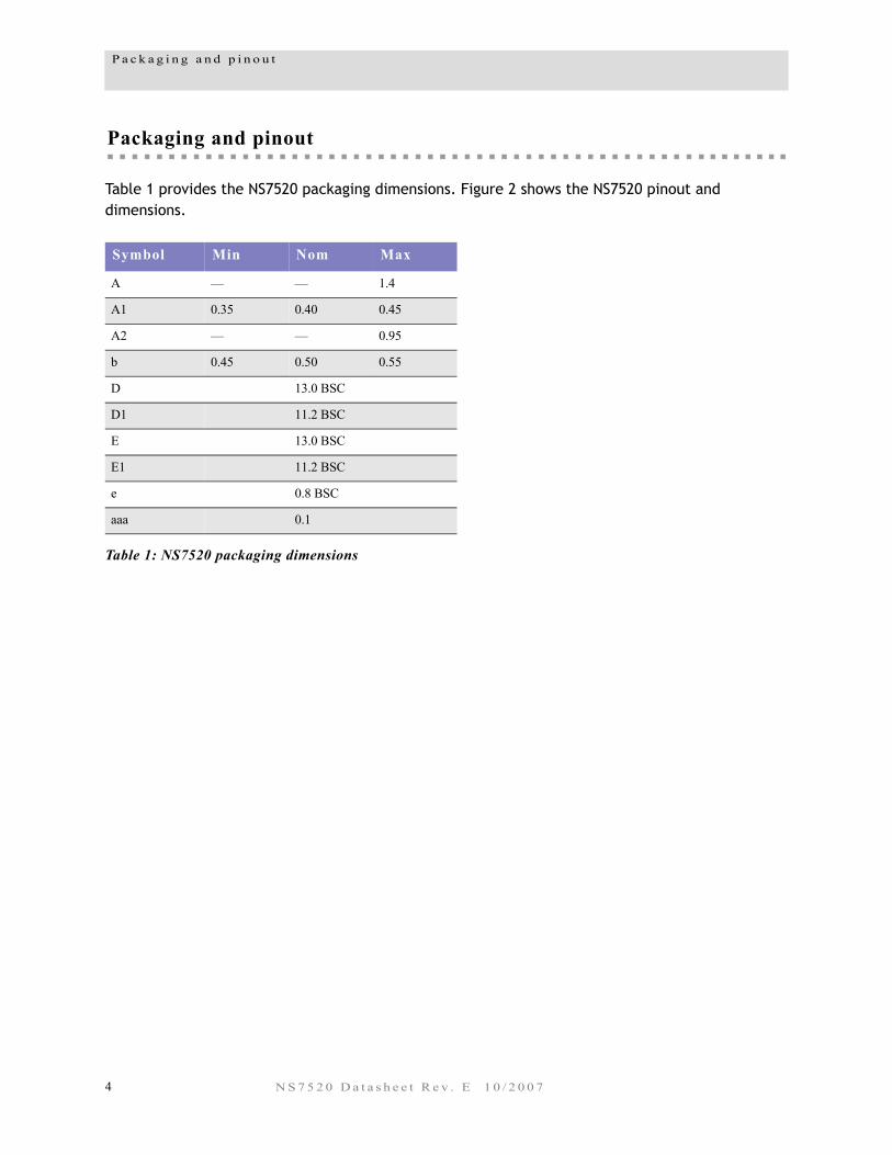
Packaging and pinout
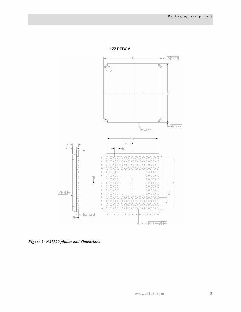
Table 1 provides the NS7520 packaging dimensions. Figure 2 shows the NS7520 pinout and dimensions.
Symbol Min Nom Max
A — — 1.4
A1 0.35 0.40 0.45
A2 — — 0.95
b 0.45 0.50 0.55
D 13.0 BSC
D1 11.2 BSC
E 13.0 BSC
E1 11.2 BSC
e 0.8 BSC
aaa 0.1
Table 1: NS7520 packaging dimensions
4 N S 7 5 2 0 D a t a s h e e t R e v . E 1 0 / 2 0 0 7
P a c k a g i n g a n d p i n o u t
Figure 2: NS7520 pinout and dimensions
177 PFBGA
w w w . d i g i . c o m 5
P i n o u t d e t a i l t a b l e s
Pinout detail tables
Each pinout table applies to a specific interface and contains the following information:
Notes:
NO CONNECT as a pin description means do not connect to this pin.
The 177th pin (package ball) is for alignment of the package on the PCB.
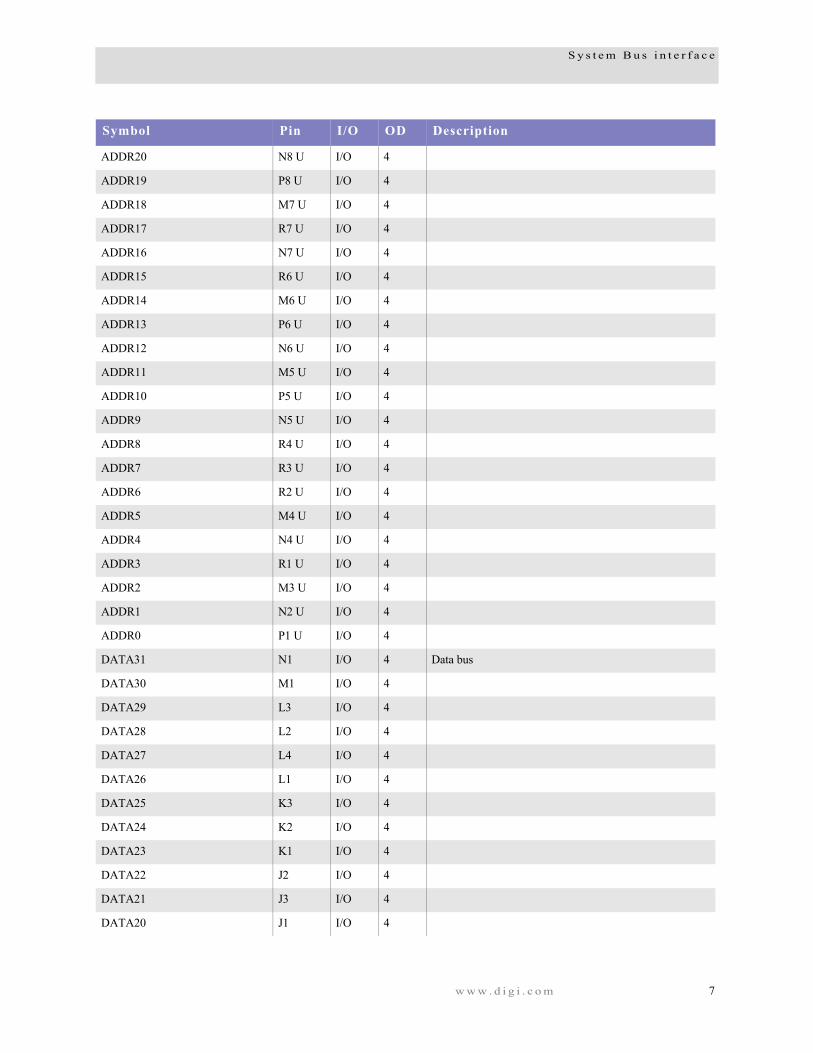
System Bus interface
Signal The pin name for each I/O signal. Some signals have multiple function modes and are identified accordingly. The mode is configured through firmware using one or more configuration registers.
Pin The pin number assignment for a specific I/O signal. U next to the pin number indicates that the pin is a pullup resistor. D next to the pin number indicates that the pin is a pulldown resistor. No value next to the pin indicates that the pin has neither a pullup nor pulldown resistor.
See Figure 5, "Internal pullup characteristics," on page 24 and Figure 6, "Internal pulldown characteristics," on page 25 for an illustration of the characteristics of these pins. Use the figures to select the appropriate value of the complimentary resistor to drive the signal to the opposite logic state. For those pins with no pullup or pulldown resistor, you must select the appropriate value per your design requirements.
_ An underscore (bar) indicates that the pin is active low.
I/O The type of signal — input, output, or input/output.
OD The output drive strength of an output buffer. The NS7520 uses one of three drivers: 2 mA 4 mA 8 mA
Symbol Pin I/O OD Description
BCLK A6 0 8 Synchronous bus clock
External bus Other External bus Other
ADDR27 CS0OE_ N10 U I/O 4 Addr bit 27 Logical AND of CS0_ and OE_
ADDR26 CS0WE_ P10 U I/O 4 Addr bit 26 Logical AND of CS_ and WE_
External bus External bus
ADDR25 M10 U I/O 4 Remainder of address bus (through ADDR0)
ADDR24 R10 U I/O 4
ADDR23 N9 U I/O 4
ADDR22 R9 U I/O 4
ADDR21 M9 U I/O 4
6 N S 7 5 2 0 D a t a s h e e t R e v . E 1 0 / 2 0 0 7
S y s t e m B u s i n t e r f a c e
ADDR20 N8 U I/O 4
ADDR19 P8 U I/O 4
ADDR18 M7 U I/O 4
ADDR17 R7 U I/O 4
ADDR16 N7 U I/O 4
ADDR15 R6 U I/O 4
ADDR14 M6 U I/O 4
ADDR13 P6 U I/O 4
ADDR12 N6 U I/O 4
ADDR11 M5 U I/O 4
ADDR10 P5 U I/O 4
ADDR9 N5 U I/O 4
ADDR8 R4 U I/O 4
ADDR7 R3 U I/O 4
ADDR6 R2 U I/O 4
ADDR5 M4 U I/O 4
ADDR4 N4 U I/O 4
ADDR3 R1 U I/O 4
ADDR2 M3 U I/O 4
ADDR1 N2 U I/O 4
ADDR0 P1 U I/O 4
DATA31 N1 I/O 4 Data bus
DATA30 M1 I/O 4
DATA29 L3 I/O 4
DATA28 L2 I/O 4
DATA27 L4 I/O 4
DATA26 L1 I/O 4
DATA25 K3 I/O 4
DATA24 K2 I/O 4
DATA23 K1 I/O 4
DATA22 J2 I/O 4
DATA21 J3 I/O 4
DATA20 J1 I/O 4
Symbol Pin I/O OD Description
w w w . d i g i . c o m 7
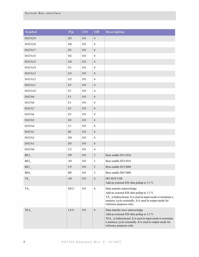
S y s t e m B u s i n t e r f a c e
DATA19 H3 I/O 4
DATA18 H4 I/O 4
DATA17 H1 I/O 4
DATA16 H2 I/O 4
DATA15 G4 I/O 4
DATA14 G1 I/O 4
DATA13 G3 I/O 4
DATA12 G2 I/O 4
DATA11 F4 I/O 4
DATA10 F2 I/O 4
DATA9 F3 I/O 4
DATA8 E1 I/O 4
DATA7 E2 I/O 4
DATA6 E3 I/O 4
DATA5 D1 I/O 4
DATA4 C1 I/O 4
DATA3 B1 I/O 4
DATA2 D4 I/O 4
DATA1 D3 I/O 4
DATA0 C2 I/O 4
BE3_ D9 I/O 2 Byte enable D31:D24
BE2_ A9 I/O 2 Byte enable D23:D16
BE1_ C9 I/O 2 Byte enable D15:D08
BE0_ B9 I/O 2 Byte enable D07:D00
TS_ A8 I/O 4 DO NOT USEAdd an external 820 ohm pullup to 3.3 V.
TA_ D8 U I/O 4 Data transfer acknowledgeAdd an external 820 ohm pullup to 3.3 V.TA_ is bidirectional. It is used in input mode to terminate a memory cycle externally. It is used in output mode for reference purposes only.
TEA_ C8 U I/O 4 Data transfer error acknowledgeAdd an external 820 ohm pullup to 3.3 V.TEA_ is bidirectional. It is used in input mode to terminate a memory cycle externally. It is used in output mode for reference purposes only.
Symbol Pin I/O OD Description
8 N S 7 5 2 0 D a t a s h e e t R e v . E 1 0 / 2 0 0 7
S y s t e m B u s i n t e r f a c e
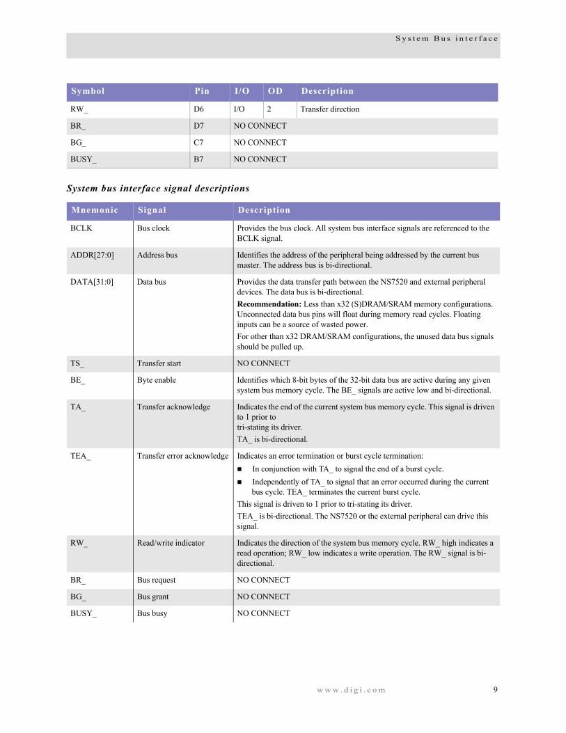
System bus interface signal descriptions
RW_ D6 I/O 2 Transfer direction
BR_ D7 NO CONNECT
BG_ C7 NO CONNECT
BUSY_ B7 NO CONNECT
Mnemonic Signal Description
BCLK Bus clock Provides the bus clock. All system bus interface signals are referenced to the BCLK signal.
ADDR[27:0] Address bus Identifies the address of the peripheral being addressed by the current bus master. The address bus is bi-directional.
DATA[31:0] Data bus Provides the data transfer path between the NS7520 and external peripheral devices. The data bus is bi-directional.Recommendation: Less than x32 (S)DRAM/SRAM memory configurations. Unconnected data bus pins will float during memory read cycles. Floating inputs can be a source of wasted power. For other than x32 DRAM/SRAM configurations, the unused data bus signals should be pulled up.
TS_ Transfer start NO CONNECT
BE_ Byte enable Identifies which 8-bit bytes of the 32-bit data bus are active during any given system bus memory cycle. The BE_ signals are active low and bi-directional.
TA_ Transfer acknowledge Indicates the end of the current system bus memory cycle. This signal is driven to 1 prior to tri-stating its driver. TA_ is bi-directional.
TEA_ Transfer error acknowledge Indicates an error termination or burst cycle termination: In conjunction with TA_ to signal the end of a burst cycle. Independently of TA_ to signal that an error occurred during the current
bus cycle. TEA_ terminates the current burst cycle. This signal is driven to 1 prior to tri-stating its driver.TEA_ is bi-directional. The NS7520 or the external peripheral can drive this signal.
RW_ Read/write indicator Indicates the direction of the system bus memory cycle. RW_ high indicates a read operation; RW_ low indicates a write operation. The RW_ signal is bi-directional.
BR_ Bus request NO CONNECT
BG_ Bus grant NO CONNECT
BUSY_ Bus busy NO CONNECT
Symbol Pin I/O OD Description
w w w . d i g i . c o m 9
C h i p s e l e c t c o n t r o l l e r
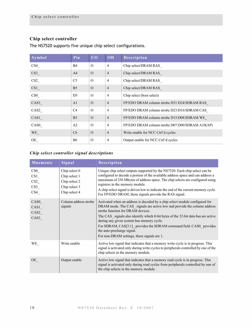
Chip select controllerThe NS7520 supports five unique chip select configurations.
Chip select controller signal descriptions
Symbol Pin I/O OD Description
CS4_ B4 O 4 Chip select/DRAM RAS_
CS3_ A4 O 4 Chip select/DRAM RAS_
CS2_ C5 O 4 Chip select/DRAM RAS_
CS1_ B5 O 4 Chip select/DRAM RAS_
CS0_ D5 O 4 Chip select (boot select)
CAS3_ A1 O 4 FP/EDO DRAM column strobe D31:D24/SDRAM RAS_
CAS2_ C4 O 4 FP/EDO DRAM column strobe D23:D16/SDRAM CAS_
CAS1_ B3 O 4 FP/EDO DRAM column strobe D15:D08/SDRAM WE_
CAS0_ A2 O 4 FP/EDO DRAM column strobe D07:D00/SDRAM A10(AP)
WE_ C6 O 4 Write enable for NCC Ctrl’d cycles
OE_ B6 O 4 Output enable for NCC Ctrl’d cycles
Mnemonic Signal Description
CS0_CS1_CS2_CS3_CS4_
Chip select 0Chip select 1Chip select 2Chip select 3Chip select 4
Unique chip select outputs supported by the NS7520. Each chip select can be configured to decode a portion of the available address space and can address a maximum of 256 Mbytes of address space. The chip selects are configured using registers in the memory module.A chip select signal is driven low to indicate the end of the current memory cycle. For FP/EDO DRAM, these signals provide the RAS signal.
CAS0_CAS1_CAS2_CAS3_
Column address strobe signals
Activated when an address is decoded by a chip select module configured for DRAM mode. The CAS_ signals are active low and provide the column address strobe function for DRAM devices.The CAS_ signals also identify which 8-bit bytes of the 32-bit data bus are active during any given system bus memory cycle.For SDRAM, CAS[3:1]_ provides the SDRAM command field. CAS0_ provides the auto-precharge signal.For non-DRAM settings, these signals are 1.
WE_ Write enable Active low signal that indicates that a memory write cycle is in progress. This signal is activated only during write cycles to peripherals controlled by one of the chip selects in the memory module.
OE_ Output enable Active low signal that indicates that a memory read cycle is in progress. This signal is activated only during read cycles from peripherals controlled by one of the chip selects in the memory module.
1 0 N S 7 5 2 0 D a t a s h e e t R e v . E 1 0 / 2 0 0 7
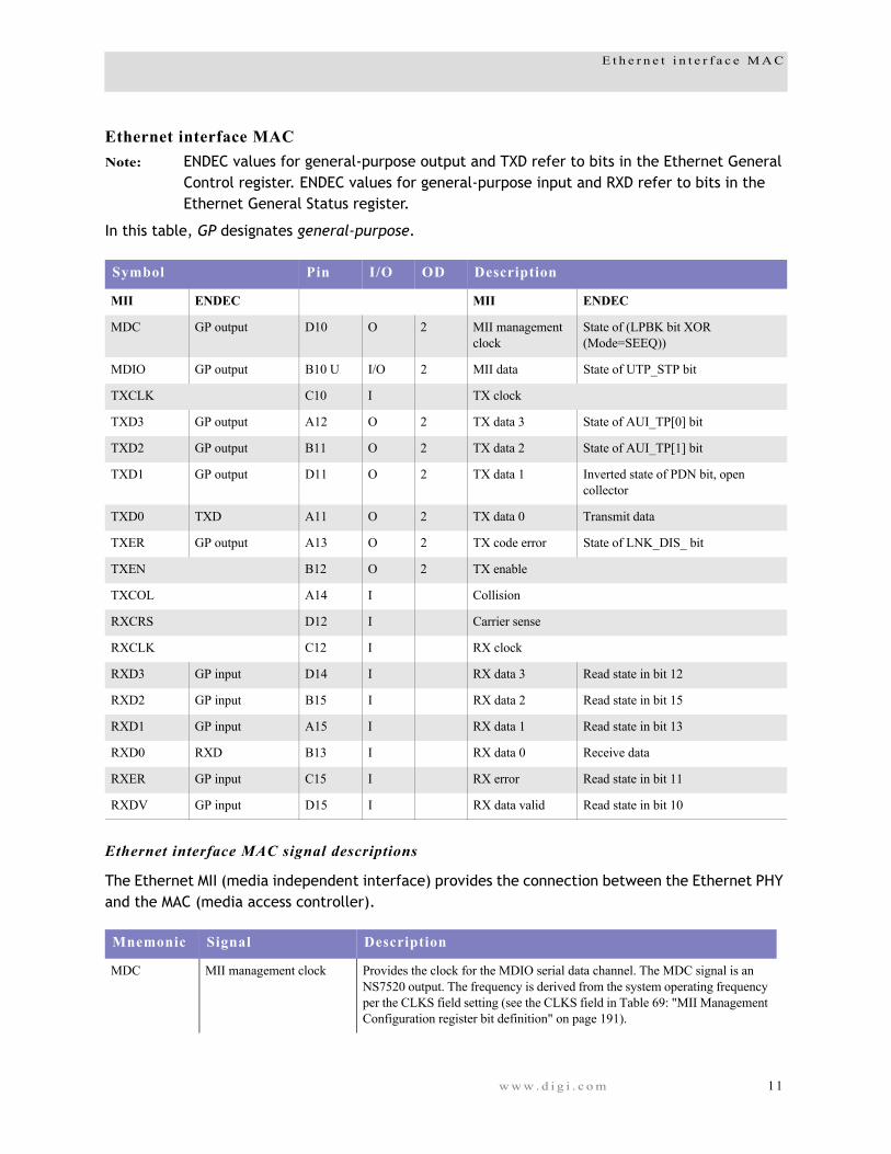
E t h e r n e t i n t e r f a c e M A C
Ethernet interface MACNote: ENDEC values for general-purpose output and TXD refer to bits in the Ethernet General
Control register. ENDEC values for general-purpose input and RXD refer to bits in the Ethernet General Status register.
In this table, GP designates general-purpose.
Ethernet interface MAC signal descriptions
The Ethernet MII (media independent interface) provides the connection between the Ethernet PHY and the MAC (media access controller).
Symbol Pin I/O OD Description
MII ENDEC MII ENDEC
MDC GP output D10 O 2 MII management clock
State of (LPBK bit XOR (Mode=SEEQ))
MDIO GP output B10 U I/O 2 MII data State of UTP_STP bit
TXCLK C10 I TX clock
TXD3 GP output A12 O 2 TX data 3 State of AUI_TP[0] bit
TXD2 GP output B11 O 2 TX data 2 State of AUI_TP[1] bit
TXD1 GP output D11 O 2 TX data 1 Inverted state of PDN bit, open collector
TXD0 TXD A11 O 2 TX data 0 Transmit data
TXER GP output A13 O 2 TX code error State of LNK_DIS_ bit
TXEN B12 O 2 TX enable
TXCOL A14 I Collision
RXCRS D12 I Carrier sense
RXCLK C12 I RX clock
RXD3 GP input D14 I RX data 3 Read state in bit 12
RXD2 GP input B15 I RX data 2 Read state in bit 15
RXD1 GP input A15 I RX data 1 Read state in bit 13
RXD0 RXD B13 I RX data 0 Receive data
RXER GP input C15 I RX error Read state in bit 11
RXDV GP input D15 I RX data valid Read state in bit 10
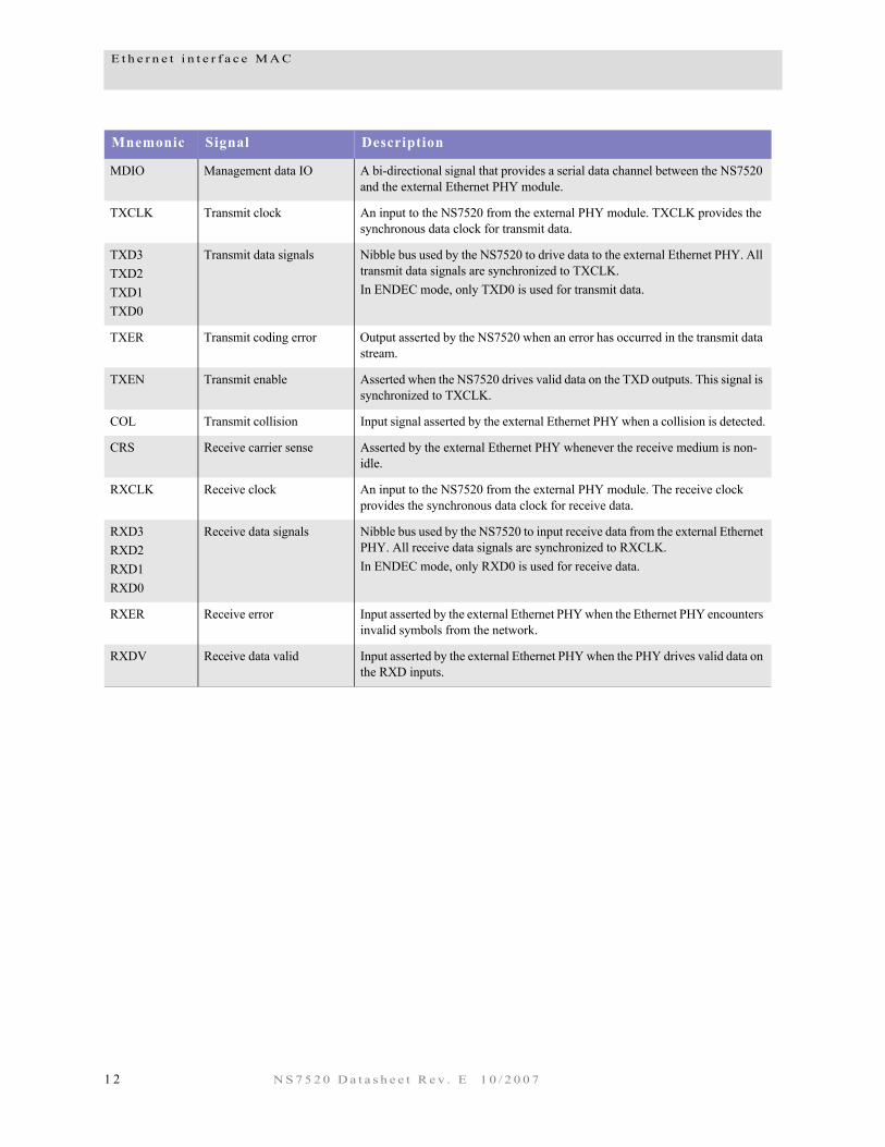
Mnemonic Signal Description
MDC MII management clock Provides the clock for the MDIO serial data channel. The MDC signal is an NS7520 output. The frequency is derived from the system operating frequency per the CLKS field setting (see the CLKS field in Table 69: "MII Management Configuration register bit definition" on page 191).
w w w . d i g i . c o m 1 1
E t h e r n e t i n t e r f a c e M A C
MDIO Management data IO A bi-directional signal that provides a serial data channel between the NS7520 and the external Ethernet PHY module.
TXCLK Transmit clock An input to the NS7520 from the external PHY module. TXCLK provides the synchronous data clock for transmit data.
TXD3TXD2TXD1TXD0
Transmit data signals Nibble bus used by the NS7520 to drive data to the external Ethernet PHY. All transmit data signals are synchronized to TXCLK. In ENDEC mode, only TXD0 is used for transmit data.
TXER Transmit coding error Output asserted by the NS7520 when an error has occurred in the transmit data stream.
TXEN Transmit enable Asserted when the NS7520 drives valid data on the TXD outputs. This signal is synchronized to TXCLK.
COL Transmit collision Input signal asserted by the external Ethernet PHY when a collision is detected.
CRS Receive carrier sense Asserted by the external Ethernet PHY whenever the receive medium is non-idle.
RXCLK Receive clock An input to the NS7520 from the external PHY module. The receive clock provides the synchronous data clock for receive data.
RXD3RXD2RXD1RXD0
Receive data signals Nibble bus used by the NS7520 to input receive data from the external Ethernet PHY. All receive data signals are synchronized to RXCLK. In ENDEC mode, only RXD0 is used for receive data.
RXER Receive error Input asserted by the external Ethernet PHY when the Ethernet PHY encounters invalid symbols from the network.
RXDV Receive data valid Input asserted by the external Ethernet PHY when the PHY drives valid data on the RXD inputs.
Mnemonic Signal Description
1 2 N S 7 5 2 0 D a t a s h e e t R e v . E 1 0 / 2 0 0 7
“ N o c o n n e c t ” p i n s
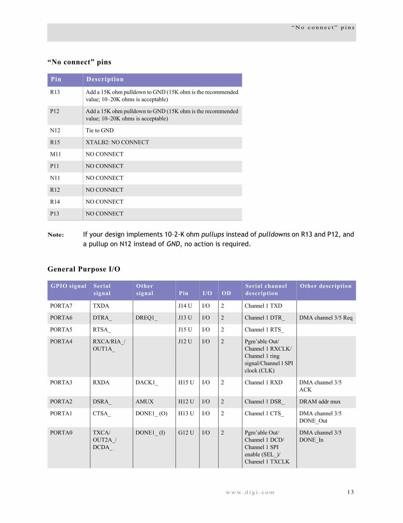
“No connect” pins
Note: If your design implements 10–2-K ohm pullups instead of pulldowns on R13 and P12, and a pullup on N12 instead of GND, no action is required.
General Purpose I/O
Pin Description
R13 Add a 15K ohm pulldown to GND (15K ohm is the recommended value; 10–20K ohms is acceptable)
P12 Add a 15K ohm pulldown to GND (15K ohm is the recommended value; 10–20K ohms is acceptable)
N12 Tie to GND
R15 XTALB2: NO CONNECT
M11 NO CONNECT
P11 NO CONNECT
N11 NO CONNECT
R12 NO CONNECT
R14 NO CONNECT
P13 NO CONNECT
GPIO signal Serialsignal
Othersignal Pin I/O OD
Serial channel description
Other description
PORTA7 TXDA J14 U I/O 2 Channel 1 TXD
PORTA6 DTRA_ DREQ1_ J13 U I/O 2 Channel 1 DTR_ DMA channel 3/5 Req
PORTA5 RTSA_ J15 U I/O 2 Channel 1 RTS_
PORTA4 RXCA/RIA_/OUT1A_
J12 U I/O 2 Pgm’able Out/Channel 1 RXCLK/ Channel 1 ring signal/Channel 1 SPI clock (CLK)
PORTA3 RXDA DACK1_ H15 U I/O 2 Channel 1 RXD DMA channel 3/5 ACK
PORTA2 DSRA_ AMUX H12 U I/O 2 Channel 1 DSR_ DRAM addr mux
PORTA1 CTSA_ DONE1_ (O) H13 U I/O 2 Channel 1 CTS_ DMA channel 3/5 DONE_Out
PORTA0 TXCA/OUT2A_/DCDA_
DONE1_ (I) G12 U I/O 2 Pgm’able Out/Channel 1 DCD/Channel 1 SPI enable (SEL_)/Channel 1 TXCLK
DMA channel 3/5 DONE_In
w w w . d i g i . c o m 1 3
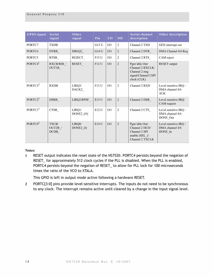
G e n e r a l P u r p o s e I / O
Notes:1 RESET output indicates the reset state of the NS7520. PORTC4 persists beyond the negation of
RESET_ for approximately 512 clock cycles if the PLL is disabled. When the PLL is enabled, PORTC4 persists beyond the negation of RESET_ to allow for PLL lock for 100 microseconds times the ratio of the VCO to XTALA.
This GPIO is left in output mode active following a hardware RESET.
2 PORTC[3:0] pins provide level-sensitive interrupts. The inputs do not need to be synchronous to any clock. The interrupt remains active until cleared by a change in the input signal level.
PORTC7 TXDB G13 U I/O 2 Channel 2 TXD GEN interrupt out
PORTC6 DTRB_ DREQ2_ G14 U I/O 2 Channel 2 DTR_ DMA Channel 4/6 Req
PORTC5 RTSB_ REJECT_ F15 U I/O 2 Channel 2 RTS_ CAM reject
PORTC41 RXCB/RIB_/OUT1B_
RESET_ F12 U I/O 2 Pgm’able Out/Channel 2 RXCLK/Channel 2 ring signal/Channel 2 SPI clock (CLK)
RESET output
PORTC32 RXDB LIRQ3/DACK2_
F13 U I/O 2 Channel 2 RXD Level sensitive IRQ / DMA channel 4/6 ACK
PORTC22 DSRB_ LIRQ2/RPSF_ E15 U I/O 2 Channel 2 DSR_ Level sensitive IRQ/CAM request
PORTC12 CTSB_ LIRQ1/DONE2_(O)
E12 U I/O 2 Channel 2 CTS_ Level sensitive IRQ / DMA channel 4/6 DONE_Out
PORTC02 TXCB/OUT2B_/DCDB_
LIRQ0/DONE2_(I)
E14 U I/O 2 Pgm’able Out/Channel 2 DCD/Channel 2 SPI enable (SEL_)/Channel 2 TXCLK
Level sensitive IRQ / DMA channel 4/6 DONE_In
GPIO signal Serialsignal
Othersignal Pin I/O OD
Serial channel description
Other description
1 4 N S 7 5 2 0 D a t a s h e e t R e v . E 1 0 / 2 0 0 7
S y s t e m c l o c k a n d r e s e t
System clock and reset
Signal descriptions
The NS7520 has three clock domains:
System clock (SYSCLK)
Bit rate generation and programmable timer reference clock (XTALA1/2)
System bus clock (BCLK)
The SYS module provides the NS7520 with these clocks, as well as system reset and backup resources.
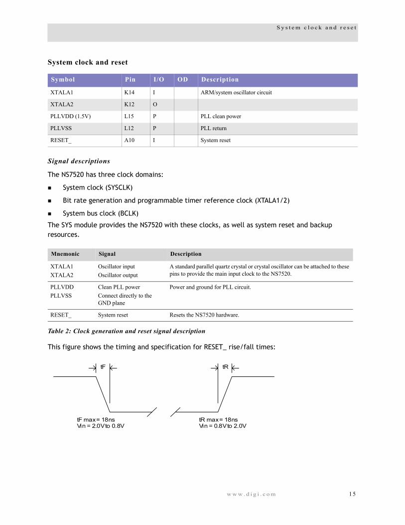
This figure shows the timing and specification for RESET_ rise/fall times:
Symbol Pin I/O OD Description
XTALA1 K14 I ARM/system oscillator circuit
XTALA2 K12 O
PLLVDD (1.5V) L15 P PLL clean power
PLLVSS L12 P PLL return
RESET_ A10 I System reset
Mnemonic Signal Description
XTALA1XTALA2
Oscillator inputOscillator output
A standard parallel quartz crystal or crystal oscillator can be attached to these pins to provide the main input clock to the NS7520.
PLLVDDPLLVSS
Clean PLL powerConnect directly to the GND plane
Power and ground for PLL circuit.
RESET_ System reset Resets the NS7520 hardware.
Table 2: Clock generation and reset signal description
tR max = 18nsVin = 0.8V to 2.0V
tF max = 18nsVin = 2.0V to 0.8V
tF tR
w w w . d i g i . c o m 1 5
S y s t e m m o d e ( t e s t s u p p o r t )
System mode (test support)PLLTST_, BISTEN_, and SCANEN_ primary inputs control different test modes for both functional and manufacturing test operations (see Table 3: "NS7520 test modes" on page 22).
JTAG testJTAG boundary scan allows a tester to check the soldering of all signal pins and tri-state all outputs.
ARM debugger signal descriptions
Symbol Pin I/O OD Description
PLLTST_ N15 I Encoded with BISTEN_ and SCANEN_Add an external pullup to 3.3V or pulldown to GND.
BISTEN_ M15 I Encoded with PLLTST_ and SCANEN_Add an external pullup to 3.3V or pulldown to GND.
SCANEN_ L13 I Encoded with BISTEN_ and PLLTST_Add an external pullup to 3.3V or pulldown to GND.
Symbol Pin I/O OD Description
TDI N14 U I Test data in.
TDO M13 O 2 Test data out.
TMS M12 U I Test mode select.
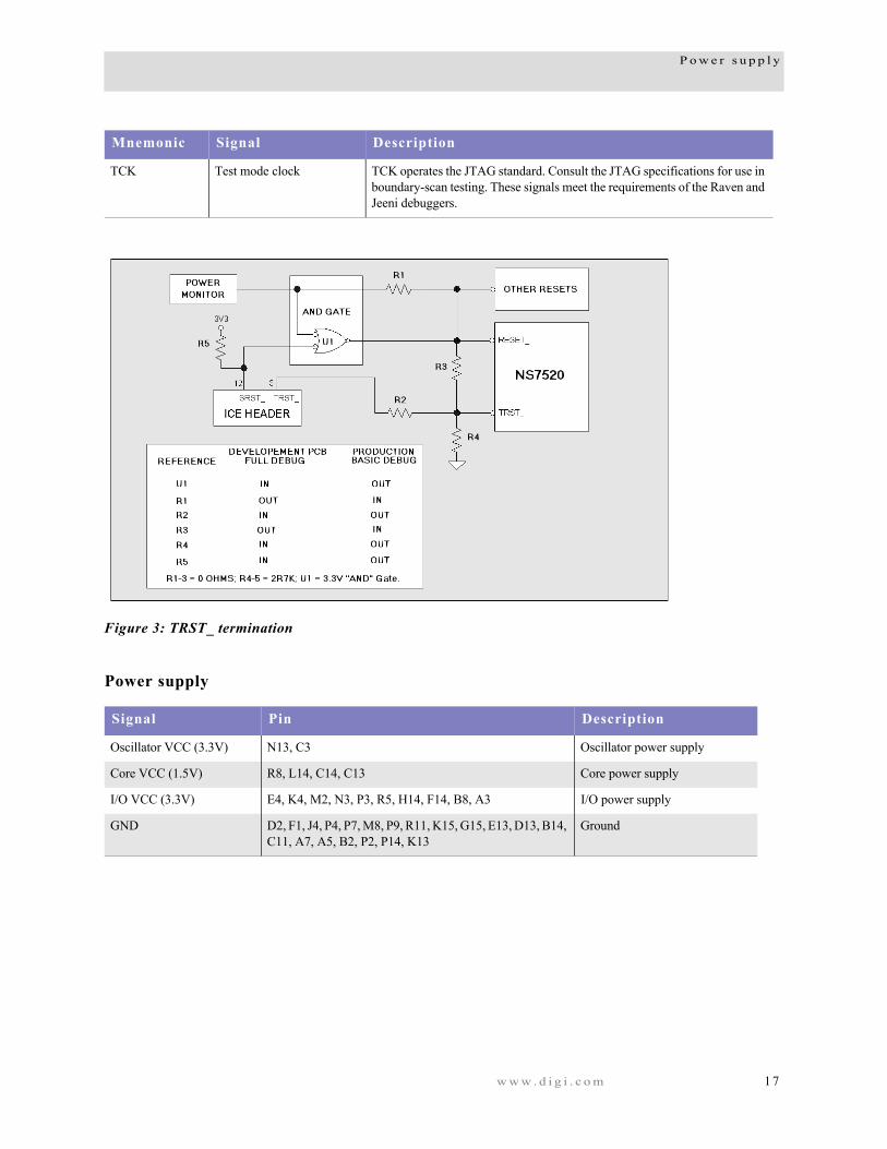
TRST_ M14 I Test mode reset.Requires external termination when not being used (see Figure 3, "TRST_ termination," on page 17 for an illustration of the termination circuit on the development PCB).
TCK P15 I Test mode clock.Add an external pullup to 3.3V.
Mnemonic Signal Description
TDI Test data in TDI operates the JTAG standard. Consult the JTAG specifications for use in boundary-scan testing. These signals meet the requirements of the Raven and Jeeni debuggers.
TDO Test data out TDO operates the JTAG standard. Consult the JTAG specifications for use in boundary-scan testing. These signals meet the requirements of the Raven and Jeeni debuggers.
TMS Test mode select TMS operates the JTAG standard. Consult the JTAG specifications for use in boundary-scan testing. These signals meet the requirements of the Raven and Jeeni debuggers.
TRST_ Test mode reset TRST_ operates the JTAG standard. Consult the JTAG specifications for use in boundary-scan testing. These signals meet the requirements of the Raven and Jeeni debuggers.
1 6 N S 7 5 2 0 D a t a s h e e t R e v . E 1 0 / 2 0 0 7
P o w e r s u p p l y
Figure 3: TRST_ termination
Power supply
TCK Test mode clock TCK operates the JTAG standard. Consult the JTAG specifications for use in boundary-scan testing. These signals meet the requirements of the Raven and Jeeni debuggers.
Signal Pin Description
Oscillator VCC (3.3V) N13, C3 Oscillator power supply
Core VCC (1.5V) R8, L14, C14, C13 Core power supply
I/O VCC (3.3V) E4, K4, M2, N3, P3, R5, H14, F14, B8, A3 I/O power supply
GND D2, F1, J4, P4, P7, M8, P9, R11, K15, G15, E13, D13, B14, C11, A7, A5, B2, P2, P14, K13
Ground
Mnemonic Signal Description
w w w . d i g i . c o m 1 7
N S 7 5 2 0 m o d u l e s
NS7520 modules
CPU moduleThe CPU uses an ARM7TDMI core processor. The ARM architecture is based on Reduced Instruction Set Computer (RISC) principles, which result in high instruction throughput and impressive real-time interrupt response for a small, cost-effective circuit. For more information about ARM7TDMI, see the ARM7TDMI Data Sheet from ARM Ltd. (www.arm.com).
GEN moduleThe GEN module provides the NS7520 with its main system control functions, as well as these features:
Two programmable timers with interrupt
One programmable bus-error timer
One programmable watchdog timer
Two 8-bit programmable general-purpose I/O ports
System (SYS) moduleThe system module provides the system clock (SYS_CLK) and system reset (SYS_RESET) resources.
The system control signals determine the basic operation of the chip:
Signal mnemonic Signal name Description
{XTALA1, XTALA2} Clock source Operate in one of two ways: The signals are affixed with a 10-20 MHz parallel mode quartz
crystal or crystal oscillator and the appropriate components per the component manufacturer. XTALA1 is driven with a clock signal and XTALA2 is left
open.
{PLLVDD, PLLVSS} PLL power Provide an isolated power supply for the PLL.
RESET_ Chip reset Active low signal asserted to initiate a hardware reset of the chip.
{TDI, TDO, TNS, TRST_, TCK}
JTAG interface Provide a JTAG interface for the chip. This interface is used for both boundary scan and ICE control of the internal processor.
{PLLTEST_, BISTEN_, SCANEN_}
Chip mode Encoded to determine the chip mode.
1 8 N S 7 5 2 0 D a t a s h e e t R e v . E 1 0 / 2 0 0 7
B B u s m o d u l e
The NS7520 clock module creates the BCLK and FXTAL signals. Both signals are used internally, but BCLK can also be accessed at ball A6 by setting the BCLKD field in the System Control register to 0.
BCLK functions as the system clock and provides the majority of the NS7520’s timing.
FXTAL provides the timing for the DRAM refresh counter, can be selected instead of BCLK to provide timing for the watchdog timer, the two internal timers, and the Serial module.
BBus moduleThe BBus module provides the data path among NS7520 internal modules. This module provides the address and data multiplexing logic that supports the data flow through the NS7520. The BBus module is the central arbiter for all the NS7520 bus masters and, once mastership is granted, handles the decoding of each address to one (or none) of the NS7520 modules.
Memory module (MEM)The MEM module provides a glueless interface to external memory devices such as Flash, DRAM, and EEPROM. The memory controller contains an integrated DRAM controller and supports five unique chip select configurations.
The MEM module monitors the BBus interface for access to the bus module; that is, any access not addressing internal resources. If the address to be used corresponds to a Base Address register in the MEM module, the MEM module provides the memory access signals and responds to the BBus with the necessary completion signal.
The MEM module can be configured to interface with FP, EDO, or SDRAM (synchronous DRAM), although the NS7520 cannot interface with more than one device type at a time.
DMA controllerThe NS7520 contains one DMA controller, with 13 DMA channels. Each DMA channel moves blocks of data between memory and a memory peripheral.
The DMA controller supports both fly-by operations and memory-to-memory operations:
When configured for fly-by operation, the DMA controller transfers data between one of the NS7520 peripherals and a memory location.
When configured for memory-to-memory operations, the DMA controller uses a temporary holding register between read and write operations. Two memory cycles are executed.
Ethernet controllerThe Ethernet controller provides the NS7520 with one IEEE 802.3u compatible Ethernet interface. The Ethernet interface includes the Ethernet front-end (EFE) and media access controller (MAC).
The Ethernet module supports both media independent interface (MII) and ENDEC modes.
w w w . d i g i . c o m 1 9
E t h e r n e t c o n t r o l l e r
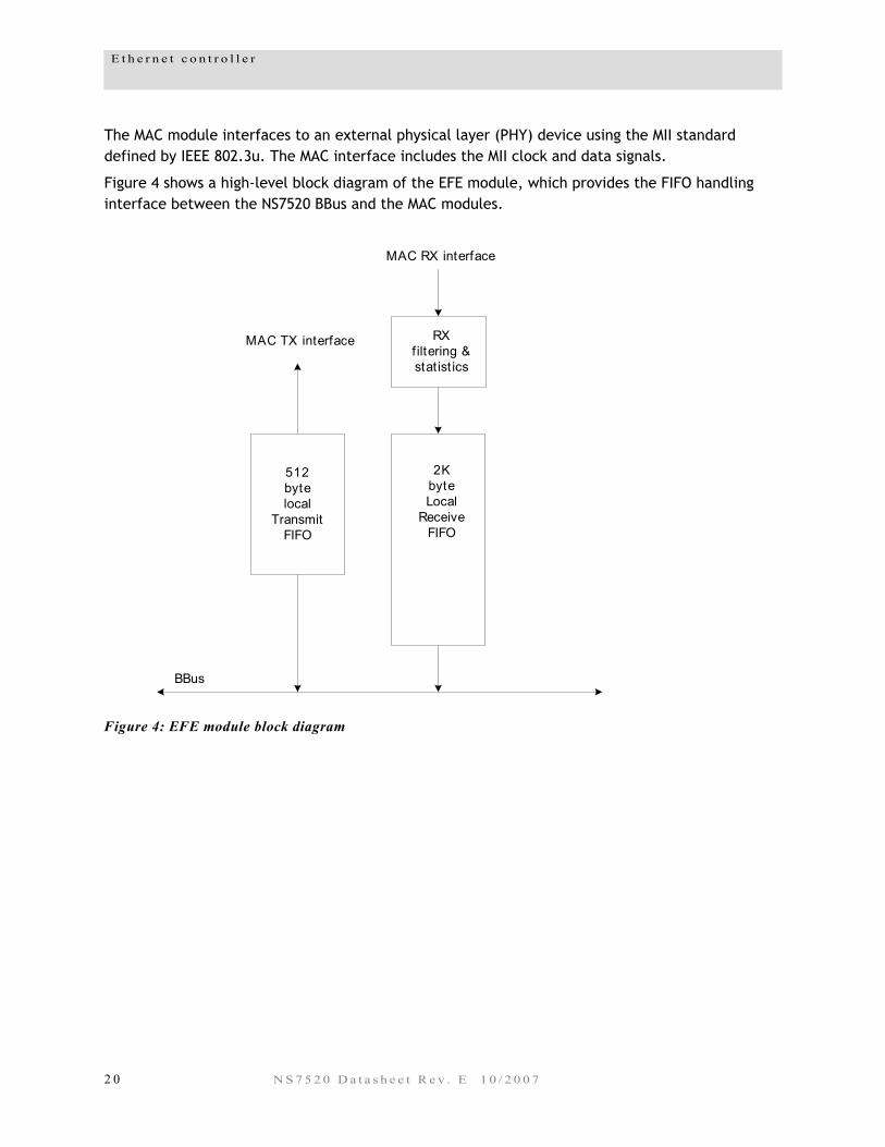
The MAC module interfaces to an external physical layer (PHY) device using the MII standard defined by IEEE 802.3u. The MAC interface includes the MII clock and data signals.
Figure 4 shows a high-level block diagram of the EFE module, which provides the FIFO handling interface between the NS7520 BBus and the MAC modules.
Figure 4: EFE module block diagram
512bytelocal
TransmitFIFO
RXfiltering &stat ist ics
2KbyteLocal
ReceiveFIFO
MAC TX interface
MAC RX interface
BBus
2 0 N S 7 5 2 0 D a t a s h e e t R e v . E 1 0 / 2 0 0 7
S e r i a l c o n t r o l l e r
Serial controllerThe NS7520 supports two independent universal asynchronous/synchronous receiver/transmitter channels. Each channel supports these features:
Independent programmable bit-rate generator
UART and SPI (master) modes
High-speed data transfer:
– x1 mode: 4Mbits/sec– x16 mode: 230 Kbits/sec
32–byte TX FIFO
32–byte RX FIFO
Programmable data format: 5–8 data bits; odd, even, or no parity; 1, 2 stop bits
Programmable channel modes: normal, local loopback, remote loopback
Control signal support
Maskable interrupt conditions:
– Receive break detection– Receive framing error– Receive parity error– Receive overrun error– Receive FIFO ready– Receive FIFO half-full– Transmit FIFO ready– Transmit FIFO half-empty– CTS, DSR, DCD, RI state change detection
Clock/data encoding: NRZ, NRZB, NRZI, FM, Manchester
Multi-drop capable
w w w . d i g i . c o m 2 1
N S 7 5 2 0 b o o t s t r a p i n i t i a l i z a t i o n
NS7520 bootstrap initialization
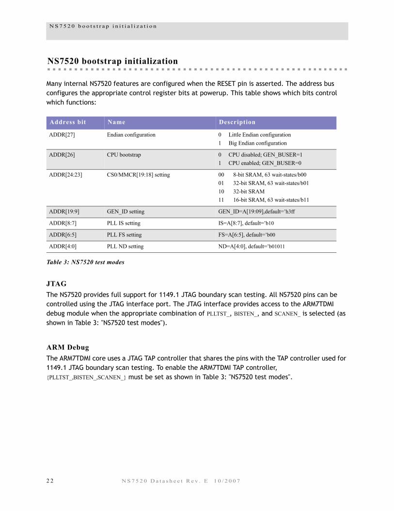
Many internal NS7520 features are configured when the RESET pin is asserted. The address bus configures the appropriate control register bits at powerup. This table shows which bits control which functions:
JTAGThe NS7520 provides full support for 1149.1 JTAG boundary scan testing. All NS7520 pins can be controlled using the JTAG interface port. The JTAG interface provides access to the ARM7TDMI debug module when the appropriate combination of PLLTST_, BISTEN_, and SCANEN_ is selected (as shown in Table 3: "NS7520 test modes").
ARM DebugThe ARM7TDMI core uses a JTAG TAP controller that shares the pins with the TAP controller used for 1149.1 JTAG boundary scan testing. To enable the ARM7TDMI TAP controller, {PLLTST_,BISTEN_,SCANEN_} must be set as shown in Table 3: "NS7520 test modes".
Address bit Name Description
ADDR[27] Endian configuration 0 Little Endian configuration1 Big Endian configuration
ADDR[26] CPU bootstrap 0 CPU disabled; GEN_BUSER=11 CPU enabled; GEN_BUSER=0
ADDR[24:23] CS0/MMCR[19:18] setting 00 8-bit SRAM, 63 wait-states/b0001 32-bit SRAM, 63 wait-states/b0110 32-bit SRAM11 16-bit SRAM, 63 wait-states/b11
ADDR[19:9] GEN_ID setting GEN_ID=A[19:09],default=’h3ff
ADDR[8:7] PLL IS setting IS=A[8:7], default=’b10
ADDR[6:5] PLL FS setting FS=A[6:5], default=’b00
ADDR[4:0] PLL ND setting ND=A[4:0], default=’b01011
Table 3: NS7520 test modes
2 2 N S 7 5 2 0 D a t a s h e e t R e v . E 1 0 / 2 0 0 7
D C c h a r a c t e r i s t i c s a n d o t h e r o p e r a t i n g s p e c i f i c a t i o n s
DC characteristics and other operating specifications
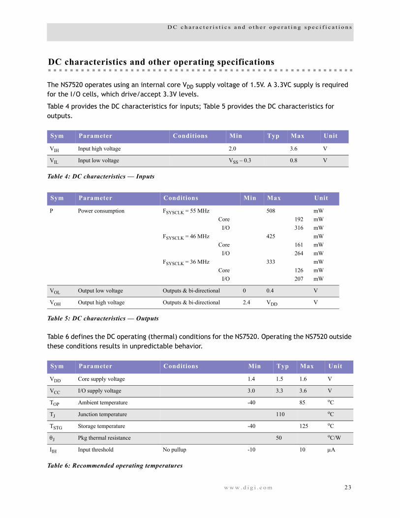
The NS7520 operates using an internal core VDD supply voltage of 1.5V. A 3.3VC supply is required for the I/O cells, which drive/accept 3.3V levels.
Table 4 provides the DC characteristics for inputs; Table 5 provides the DC characteristics for outputs.
Table 6 defines the DC operating (thermal) conditions for the NS7520. Operating the NS7520 outside these conditions results in unpredictable behavior.
Sym Parameter Conditions Min Typ Max Unit
VIH Input high voltage 2.0 3.6 V
VIL Input low voltage VSS – 0.3 0.8 V
Table 4: DC characteristics — Inputs
Sym Parameter Conditions Min Max Unit
P Power consumption FSYSCLK = 55 MHzCore
I/OFSYSCLK = 46 MHz
CoreI/O
FSYSCLK = 36 MHzCore
I/O
508192316
425161264
333126207
mWmWmWmWmWmWmWmWmW
VOL Output low voltage Outputs & bi-directional 0 0.4 V
VOH Output high voltage Outputs & bi-directional 2.4 VDD V
Table 5: DC characteristics — Outputs
Sym Parameter Conditions Min Typ Max Unit
VDD Core supply voltage 1.4 1.5 1.6 V
VCC I/O supply voltage 3.0 3.3 3.6 V
TOP Ambient temperature -40 85 oC
TJ Junction temperature 110 oC
TSTG Storage temperature -40 125 oC
θJ Pkg thermal resistance 50 oC/W
IIH Input threshold No pullup -10 10 μΑ
Table 6: Recommended operating temperatures
w w w . d i g i . c o m 2 3
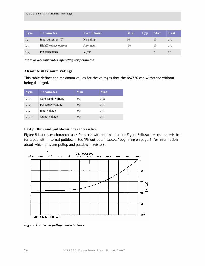
A b s o l u t e m a x i m u m r a t i n g s
Absolute maximum ratings
This table defines the maximum values for the voltages that the NS7520 can withstand without being damaged.
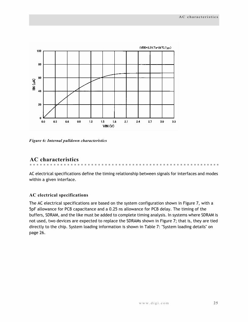
Pad pullup and pulldown characteristicsFigure 5 illustrates characteristics for a pad with internal pullup; Figure 6 illustrates characteristics for a pad with internal pulldown. See "Pinout detail tables," beginning on page 6, for information about which pins use pullup and pulldown resistors.
Figure 5: Internal pullup characteristics
IIL Input current as “0” No pullup 10 10 μA
IOZ HighZ leakage current Any input -10 10 μA
CIO Pin capacitance VO=0 7 pF
Sym Parameter Min Max
VDD Core supply voltage -0.3 3.15
VCC I/O supply voltage -0.3 3.9
VIN Input voltage -0.3 3.9
VOUT Output voltage -0.3 3.9
Sym Parameter Conditions Min Typ Max Unit
Table 6: Recommended operating temperatures
2 4 N S 7 5 2 0 D a t a s h e e t R e v . E 1 0 / 2 0 0 7
A C c h a r a c t e r i s t i c s
Figure 6: Internal pulldown characteristics
AC characteristics
AC electrical specifications define the timing relationship between signals for interfaces and modes within a given interface.
AC electrical specifications
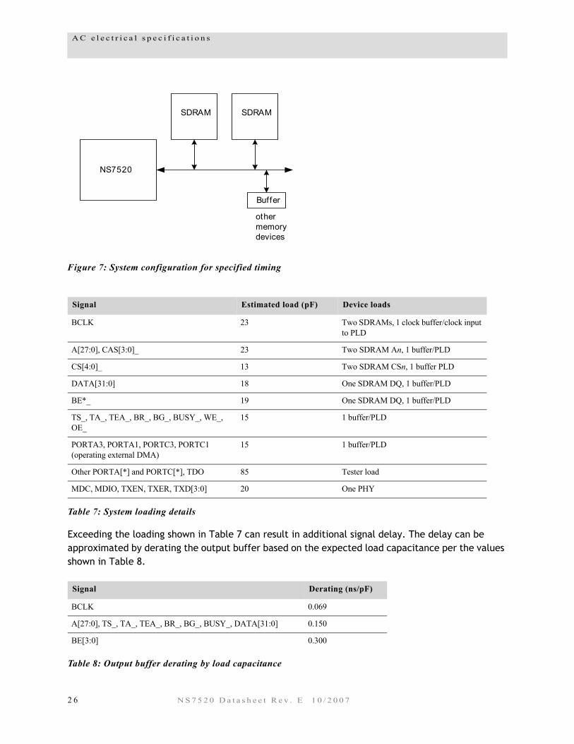
The AC electrical specifications are based on the system configuration shown in Figure 7, with a 5pF allowance for PCB capacitance and a 0.25 ns allowance for PCB delay. The timing of the buffers, SDRAM, and the like must be added to complete timing analysis. In systems where SDRAM is not used, two devices are expected to replace the SDRAMs shown in Figure 7; that is, they are tied directly to the chip. System loading information is shown in Table 7: "System loading details" on page 26.
w w w . d i g i . c o m 2 5
A C e l e c t r i c a l s p e c i f i c a t i o n s
Figure 7: System configuration for specified timing
Exceeding the loading shown in Table 7 can result in additional signal delay. The delay can be approximated by derating the output buffer based on the expected load capacitance per the values shown in Table 8.
Signal Estimated load (pF) Device loads
BCLK 23 Two SDRAMs, 1 clock buffer/clock input to PLD
A[27:0], CAS[3:0]_ 23 Two SDRAM An, 1 buffer/PLD
CS[4:0]_ 13 Two SDRAM CSn, 1 buffer PLD
DATA[31:0] 18 One SDRAM DQ, 1 buffer/PLD
BE*_ 19 One SDRAM DQ, 1 buffer/PLD
TS_, TA_, TEA_, BR_, BG_, BUSY_, WE_, OE_
15 1 buffer/PLD
PORTA3, PORTA1, PORTC3, PORTC1 (operating external DMA)
15 1 buffer/PLD
Other PORTA[*] and PORTC[*], TDO 85 Tester load
MDC, MDIO, TXEN, TXER, TXD[3:0] 20 One PHY
Table 7: System loading details
Signal Derating (ns/pF)
BCLK 0.069
A[27:0], TS_, TA_, TEA_, BR_, BG_, BUSY_, DATA[31:0] 0.150
BE[3:0] 0.300
Table 8: Output buffer derating by load capacitance
SDRAM SDRAM
NS7520
othermemorydevices
Buffer
2 6 N S 7 5 2 0 D a t a s h e e t R e v . E 1 0 / 2 0 0 7
O s c i l l a t o r C h a r a c t e r i s t i c s
Oscillator Characteristics
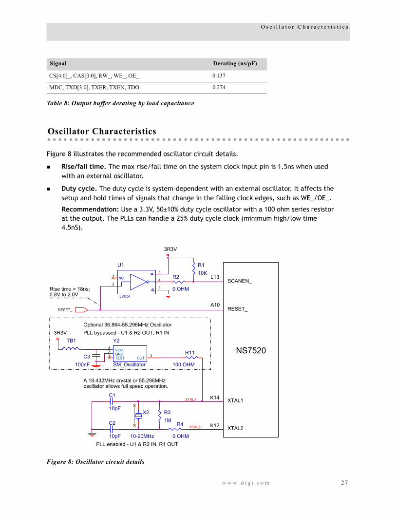
Figure 8 illustrates the recommended oscillator circuit details.
Rise/fall time. The max rise/fall time on the system clock input pin is 1.5ns when used with an external oscillator.
Duty cycle. The duty cycle is system-dependent with an external oscillator. It affects the setup and hold times of signals that change in the falling clock edges, such as WE_/OE_.
Recommendation: Use a 3.3V, 50±10% duty cycle oscillator with a 100 ohm series resistor at the output. The PLLs can handle a 25% duty cycle clock (minimum high/low time 4.5nS).
Figure 8: Oscillator circuit details
CS[4:0]_, CAS[3:0], RW_, WE_, OE_ 0.137
MDC, TXD[3:0], TXER, TXEN, TDO 0.274
Signal Derating (ns/pF)
Table 8: Output buffer derating by load capacitance
3R3V
SCANEN_
PLL enabled - U1 & R2 IN, R1 OUT
C2
10pF
A 18.432MHz crystal or 55.296MHzoscillator allows full speed operation.
R4
0 OHM
NC
U1
LVC04
1
23
4
5
RESET_
K14
3R3V
C3100nF
C1
10pF
R2
0 OHM
PLL bypassed - U1 & R2 OUT, R1 IN
R110K
Y2
SM_Oscillator
421 3
VCCGNDTEST OUT
K12
NS7520
R31M
R11
100 OHM
XTAL1
A10
Rise time = 18ns;0.8V to 2.0V
XTAL1
L13
RESET_
XTAL2
Optional 36.864-55.296MHz Oscillator
TB1
XTAL2
X2
10-20MHz
w w w . d i g i . c o m 2 7
T i m i n g D i a g r a m s
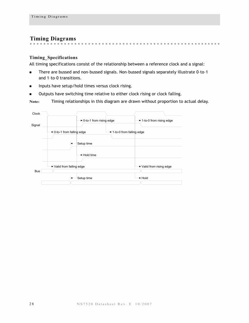
Timing Diagrams
Timing_SpecificationsAll timing specifications consist of the relationship between a reference clock and a signal:
There are bussed and non–bussed signals. Non–bussed signals separately illustrate 0–to–1 and 1–to–0 transitions.
Inputs have setup/hold times versus clock rising.
Outputs have switching time relative to either clock rising or clock falling.
Note: Timing relationships in this diagram are drawn without proportion to actual delay.
HoldSetup time
Valid from rising edgeValid from falling edge
Hold time
Setup time
1-to-0 from falling edge0-to-1 from falling edge
1-to-0 from rising edge0-to-1 from rising edge
Clock
Signal
Bus
2 8 N S 7 5 2 0 D a t a s h e e t R e v . E 1 0 / 2 0 0 7
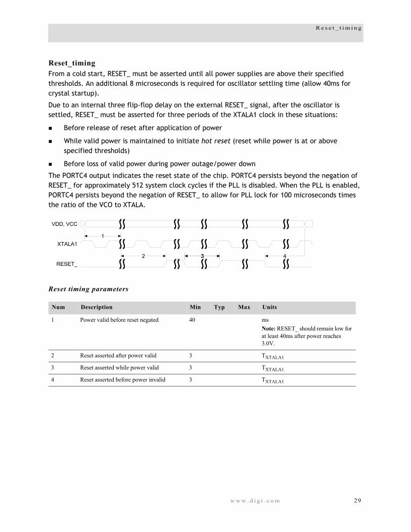
R e s e t _ t i m i n g
Reset_timingFrom a cold start, RESET_ must be asserted until all power supplies are above their specified thresholds. An additional 8 microseconds is required for oscillator settling time (allow 40ms for crystal startup).
Due to an internal three flip-flop delay on the external RESET_ signal, after the oscillator is settled, RESET_ must be asserted for three periods of the XTALA1 clock in these situations:
Before release of reset after application of power
While valid power is maintained to initiate hot reset (reset while power is at or above specified thresholds)
Before loss of valid power during power outage/power down
The PORTC4 output indicates the reset state of the chip. PORTC4 persists beyond the negation of RESET_ for approximately 512 system clock cycles if the PLL is disabled. When the PLL is enabled, PORTC4 persists beyond the negation of RESET_ to allow for PLL lock for 100 microseconds times the ratio of the VCO to XTALA.
Reset timing parameters
Num Description Min Typ Max Units
1 Power valid before reset negated 40 msNote: RESET_ should remain low for at least 40ms after power reaches 3.0V.
2 Reset asserted after power valid 3 TXTALA1
3 Reset asserted while power valid 3 TXTALA1
4 Reset asserted before power invalid 3 TXTALA1
4332
1
VDD, VCC
XTALA1
RESET_
w w w . d i g i . c o m 2 9
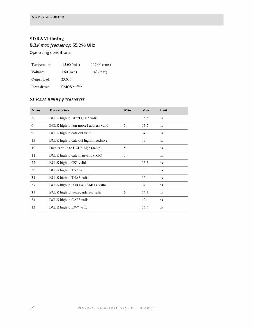
S R A M t i m i n g
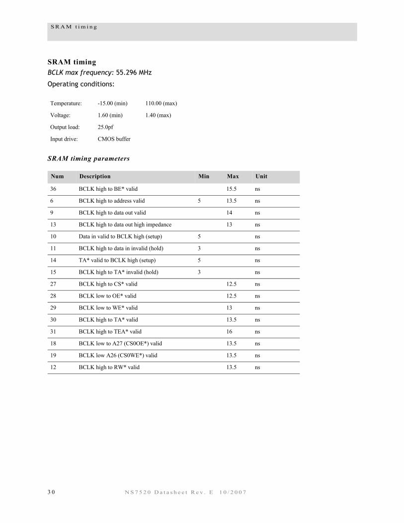
SRAM timingBCLK max frequency: 55.296 MHz
Operating conditions:
SRAM timing parameters
Temperature: -15.00 (min) 110.00 (max)
Voltage: 1.60 (min) 1.40 (max)
Output load: 25.0pf
Input drive: CMOS buffer
Num Description Min Max Unit
36 BCLK high to BE* valid 15.5 ns
6 BCLK high to address valid 5 13.5 ns
9 BCLK high to data out valid 14 ns
13 BCLK high to data out high impedance 13 ns
10 Data in valid to BCLK high (setup) 5 ns
11 BCLK high to data in invalid (hold) 3 ns
14 TA* valid to BCLK high (setup) 5 ns
15 BCLK high to TA* invalid (hold) 3 ns
27 BCLK high to CS* valid 12.5 ns
28 BCLK low to OE* valid 12.5 ns
29 BCLK low to WE* valid 13 ns
30 BCLK high to TA* valid 13.5 ns
31 BCLK high to TEA* valid 16 ns
18 BCLK low to A27 (CS0OE*) valid 13.5 ns
19 BCLK low A26 (CS0WE*) valid 13.5 ns
12 BCLK high to RW* valid 13.5 ns
3 0 N S 7 5 2 0 D a t a s h e e t R e v . E 1 0 / 2 0 0 7
S R A M t i m i n g
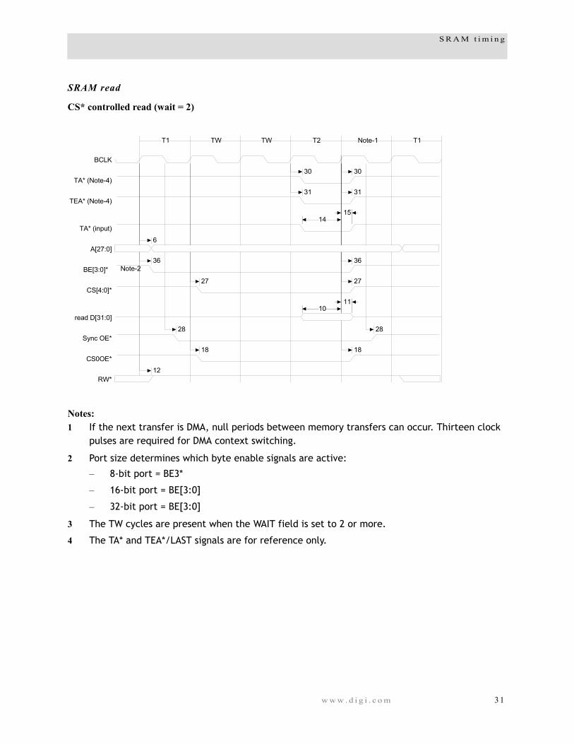
SRAM read
CS* controlled read (wait = 2)
Notes:1 If the next transfer is DMA, null periods between memory transfers can occur. Thirteen clock
pulses are required for DMA context switching.
2 Port size determines which byte enable signals are active:
– 8-bit port = BE3*
– 16-bit port = BE[3:0]
– 32-bit port = BE[3:0]
3 The TW cycles are present when the WAIT field is set to 2 or more.
4 The TA* and TEA*/LAST signals are for reference only.
T1 TW TW T2 Note-1 T1
12
1818
2828
2727
3636
6
3131
3030
1110
1514
Note-2
BCLK
TA* (Note-4)
TEA* (Note-4)
TA* (input)
A[27:0]
BE[3:0]*
CS[4:0]*
read D[31:0]
Sync OE*
CS0OE*
RW*
w w w . d i g i . c o m 3 1
S R A M t i m i n g
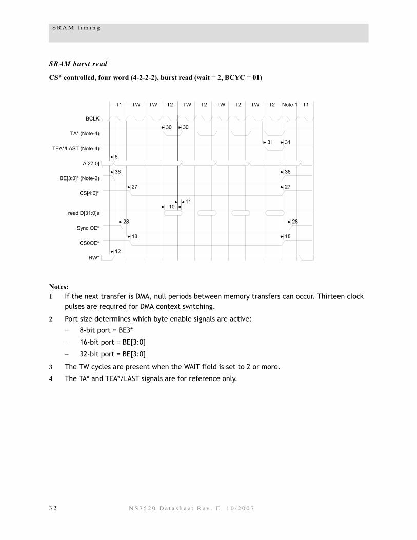
SRAM burst read
CS* controlled, four word (4-2-2-2), burst read (wait = 2, BCYC = 01)
Notes:1 If the next transfer is DMA, null periods between memory transfers can occur. Thirteen clock
pulses are required for DMA context switching.
2 Port size determines which byte enable signals are active:
– 8-bit port = BE3*
– 16-bit port = BE[3:0]
– 32-bit port = BE[3:0]
3 The TW cycles are present when the WAIT field is set to 2 or more.
4 The TA* and TEA*/LAST signals are for reference only.
T1 TW TW T2 TW T2 TW T2 TW T2 Note-1 T1
12
1818
2828
2727
3636
6
3131
3030
1110
BCLK
TA* (Note-4)
TEA*/LAST (Note-4)
A[27:0]
BE[3:0]* (Note-2)
CS[4:0]*
read D[31:0]s
Sync OE*
CS0OE*
RW*
3 2 N S 7 5 2 0 D a t a s h e e t R e v . E 1 0 / 2 0 0 7
S R A M t i m i n g
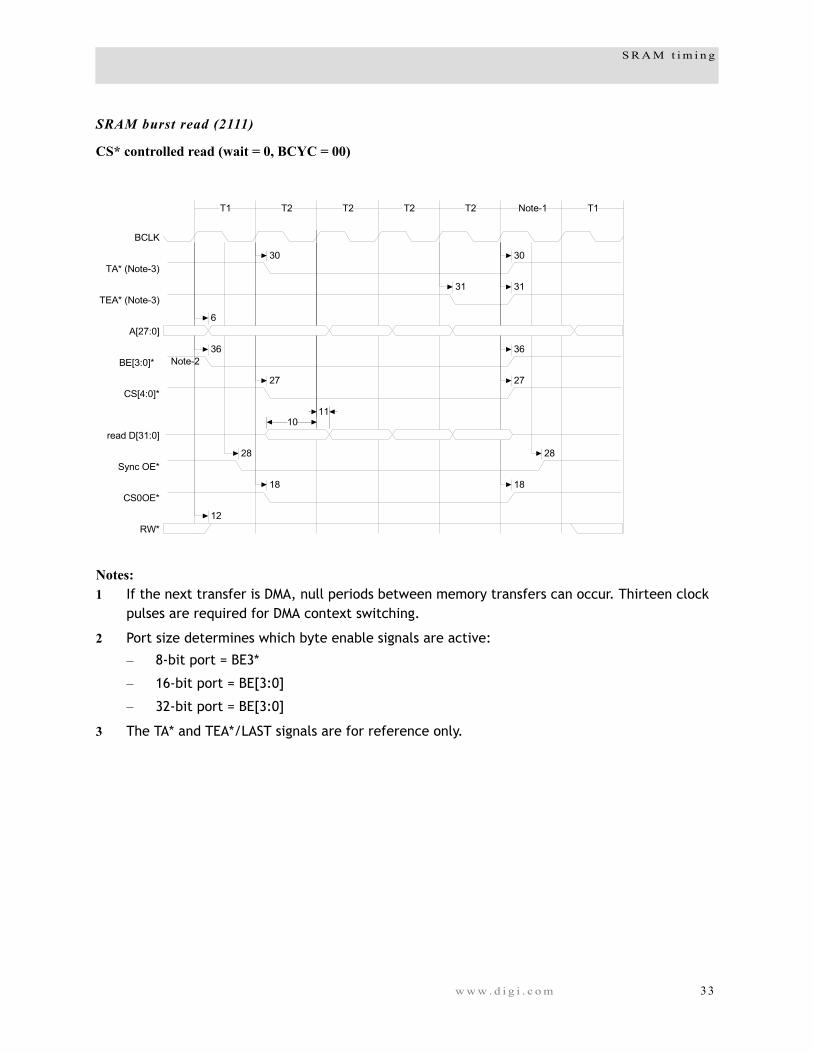
SRAM burst read (2111)
CS* controlled read (wait = 0, BCYC = 00)
Notes:1 If the next transfer is DMA, null periods between memory transfers can occur. Thirteen clock
pulses are required for DMA context switching.
2 Port size determines which byte enable signals are active:
– 8-bit port = BE3*
– 16-bit port = BE[3:0]
– 32-bit port = BE[3:0]
3 The TA* and TEA*/LAST signals are for reference only.
T1 T2 T2 T2 T2 Note-1 T1
12
1818
2828
2727
3636
6
3131
3030
1110
Note-2
BCLK
TA* (Note-3)
TEA* (Note-3)
A[27:0]
BE[3:0]*
CS[4:0]*
read D[31:0]
Sync OE*
CS0OE*
RW*
w w w . d i g i . c o m 3 3
S R A M t i m i n g
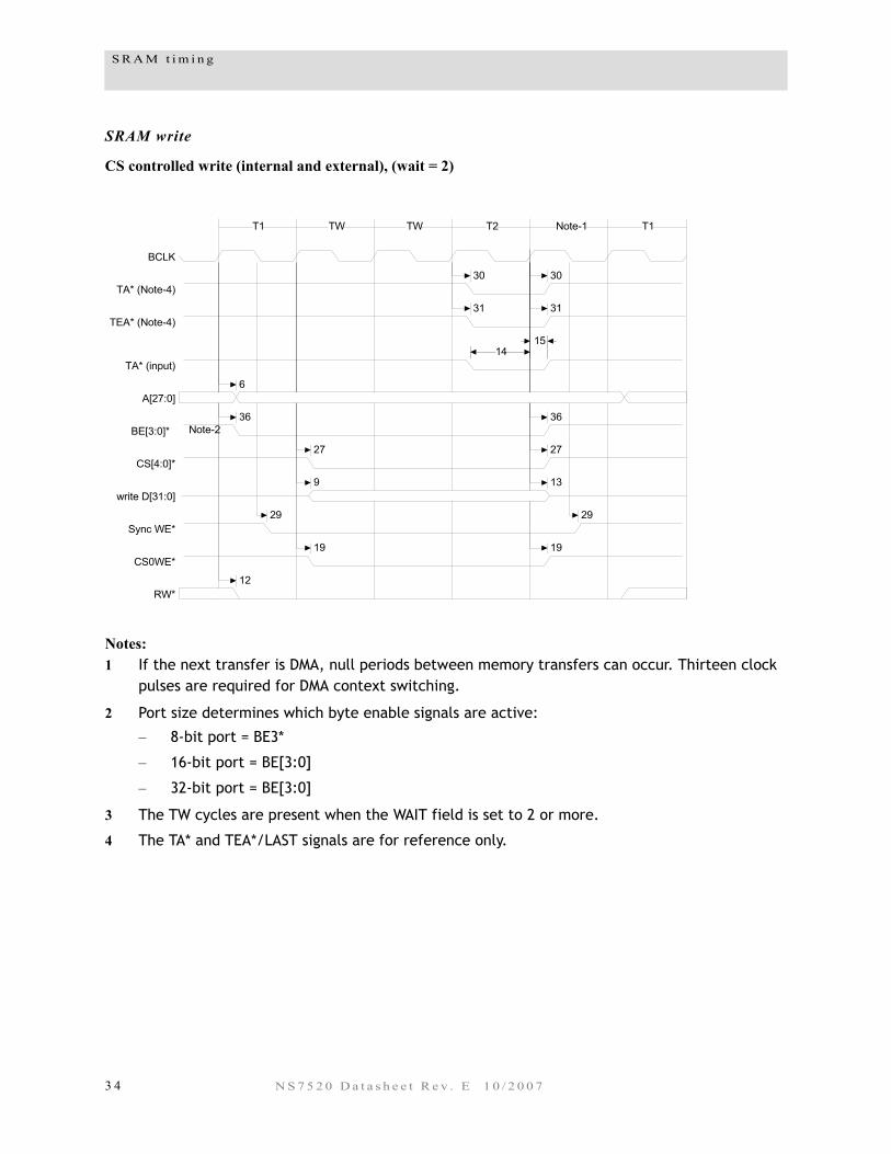
SRAM write
CS controlled write (internal and external), (wait = 2)
Notes:1 If the next transfer is DMA, null periods between memory transfers can occur. Thirteen clock
pulses are required for DMA context switching.
2 Port size determines which byte enable signals are active:
– 8-bit port = BE3*
– 16-bit port = BE[3:0]
– 32-bit port = BE[3:0]
3 The TW cycles are present when the WAIT field is set to 2 or more.
4 The TA* and TEA*/LAST signals are for reference only.
T1 TW TW T2 Note-1 T1
12
1919
2929
139
2727
3636
6
3131
3030
1514
Note-2
BCLK
TA* (Note-4)
TEA* (Note-4)
TA* (input)
A[27:0]
BE[3:0]*
CS[4:0]*
write D[31:0]
Sync WE*
CS0WE*
RW*
3 4 N S 7 5 2 0 D a t a s h e e t R e v . E 1 0 / 2 0 0 7

S R A M t i m i n g
SRAM burst write
CS controlled, four word (4-2-2-2), burst write (wait = 2, BCYC = 01)
Notes:1 If the next transfer is DMA, null periods between memory transfers can occur. Thirteen clock
pulses are required for DMA context switching.
2 Port size determines which byte enable signals are active:
– 8-bit port = BE3*
– 16-bit port = BE[3:0]
– 32-bit port = BE[3:0]
3 The TW cycles are present when the WAIT field is set to 2 or more.
4 The TA* and TEA*/LAST signals are for reference only.
T1 TW TW T2 TW T2 TW T2 TW T2 Note-1 T1
12
1919
2929
139
2727
3636
6
3131
3030
BCLK
TA* (Note-4)
TEA*/LAST (Note-4)
A[27:0]
BE[3:0]* (Note-2)
CS[4:0]*
write D[31:0]
Sync WE*
CS0WE*
RW*
w w w . d i g i . c o m 3 5
S R A M t i m i n g
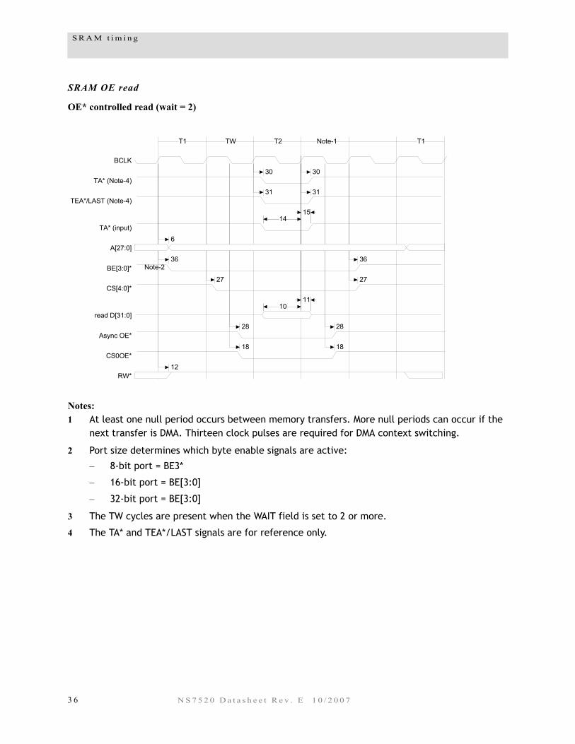
SRAM OE read
OE* controlled read (wait = 2)
Notes:1 At least one null period occurs between memory transfers. More null periods can occur if the
next transfer is DMA. Thirteen clock pulses are required for DMA context switching.
2 Port size determines which byte enable signals are active:
– 8-bit port = BE3*
– 16-bit port = BE[3:0]
– 32-bit port = BE[3:0]
3 The TW cycles are present when the WAIT field is set to 2 or more.
4 The TA* and TEA*/LAST signals are for reference only.
T1 TW T2 Note-1 T1
12
1818
2828
2727
3636
6
3131
3030
1110
1514
Note-2
BCLK
TA* (Note-4)
TEA*/LAST (Note-4)
TA* (input)
A[27:0]
BE[3:0]*
CS[4:0]*
read D[31:0]
Async OE*
CS0OE*
RW*
3 6 N S 7 5 2 0 D a t a s h e e t R e v . E 1 0 / 2 0 0 7
S R A M t i m i n g
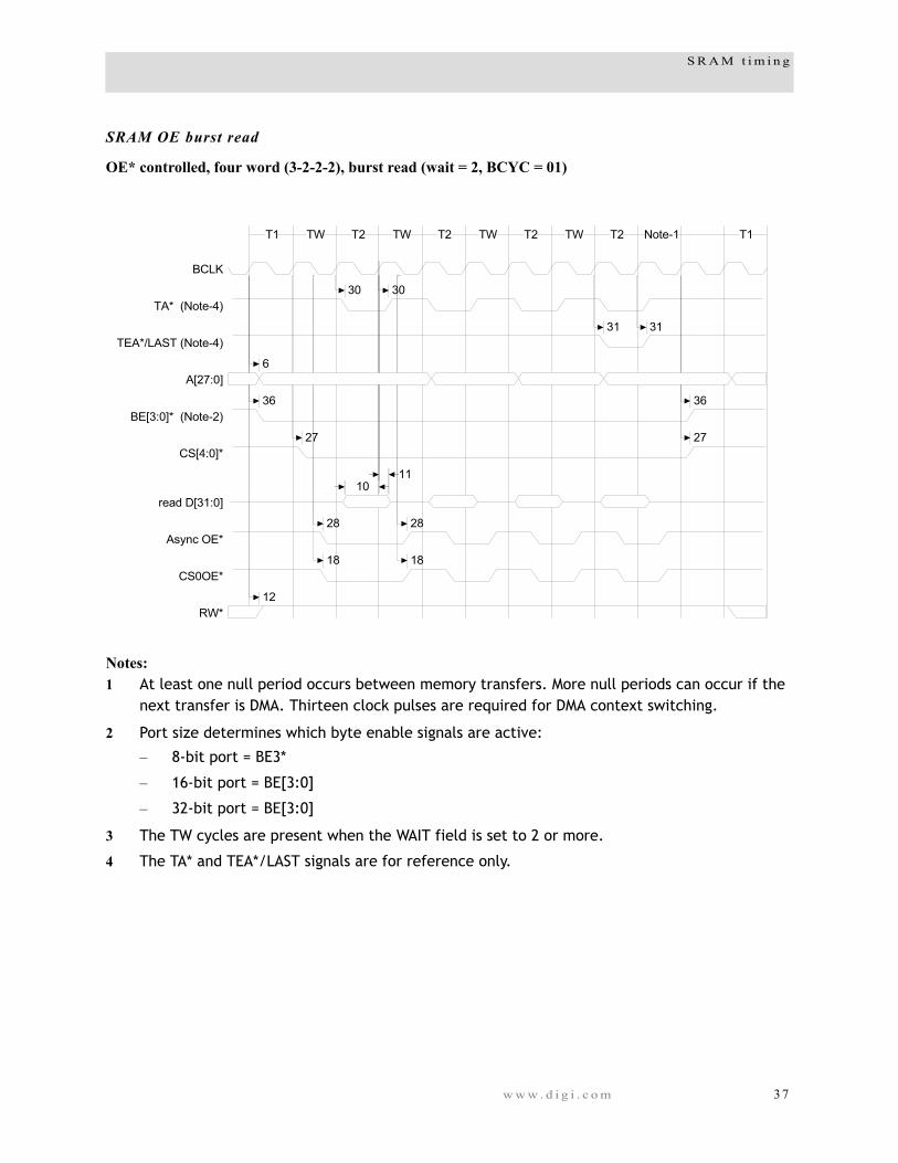
SRAM OE burst read
OE* controlled, four word (3-2-2-2), burst read (wait = 2, BCYC = 01)
Notes:1 At least one null period occurs between memory transfers. More null periods can occur if the
next transfer is DMA. Thirteen clock pulses are required for DMA context switching.
2 Port size determines which byte enable signals are active:
– 8-bit port = BE3*
– 16-bit port = BE[3:0]
– 32-bit port = BE[3:0]
3 The TW cycles are present when the WAIT field is set to 2 or more.
4 The TA* and TEA*/LAST signals are for reference only.
T1 TW T2 TW T2 TW T2 TW T2 Note-1 T1
12
1818
2828
2727
3636
6
3131
3030
1110
BCLK
TA* (Note-4)
TEA*/LAST (Note-4)
A[27:0]
BE[3:0]* (Note-2)
CS[4:0]*
read D[31:0]
Async OE*
CS0OE*
RW*
w w w . d i g i . c o m 3 7
S R A M t i m i n g
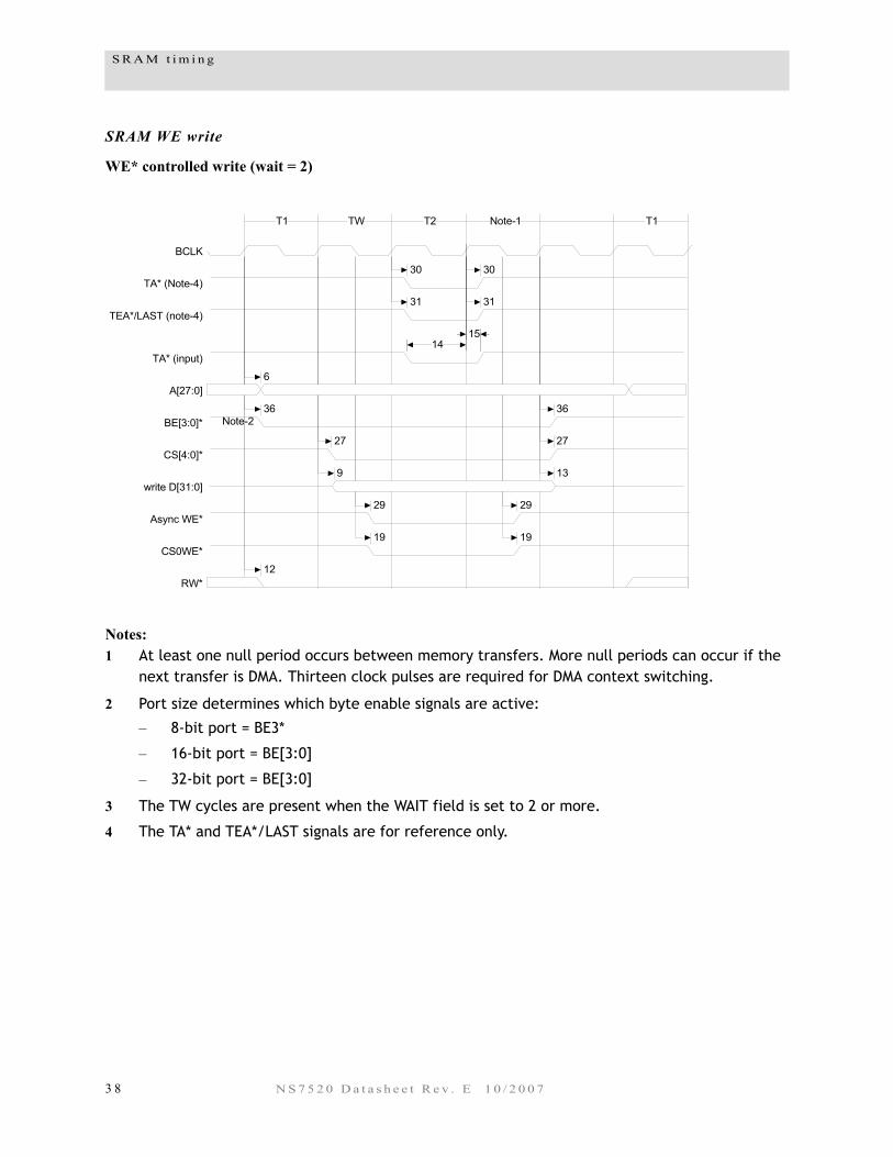
SRAM WE write
WE* controlled write (wait = 2)
Notes:1 At least one null period occurs between memory transfers. More null periods can occur if the
next transfer is DMA. Thirteen clock pulses are required for DMA context switching.
2 Port size determines which byte enable signals are active:
– 8-bit port = BE3*
– 16-bit port = BE[3:0]
– 32-bit port = BE[3:0]
3 The TW cycles are present when the WAIT field is set to 2 or more.
4 The TA* and TEA*/LAST signals are for reference only.
T1 TW T2 Note-1 T1
12
1919
2929
139
2727
3636
6
3131
3030
1514
Note-2
BCLK
TA* (Note-4)
TEA*/LAST (note-4)
TA* (input)
A[27:0]
BE[3:0]*
CS[4:0]*
write D[31:0]
Async WE*
CS0WE*
RW*
3 8 N S 7 5 2 0 D a t a s h e e t R e v . E 1 0 / 2 0 0 7
S R A M t i m i n g
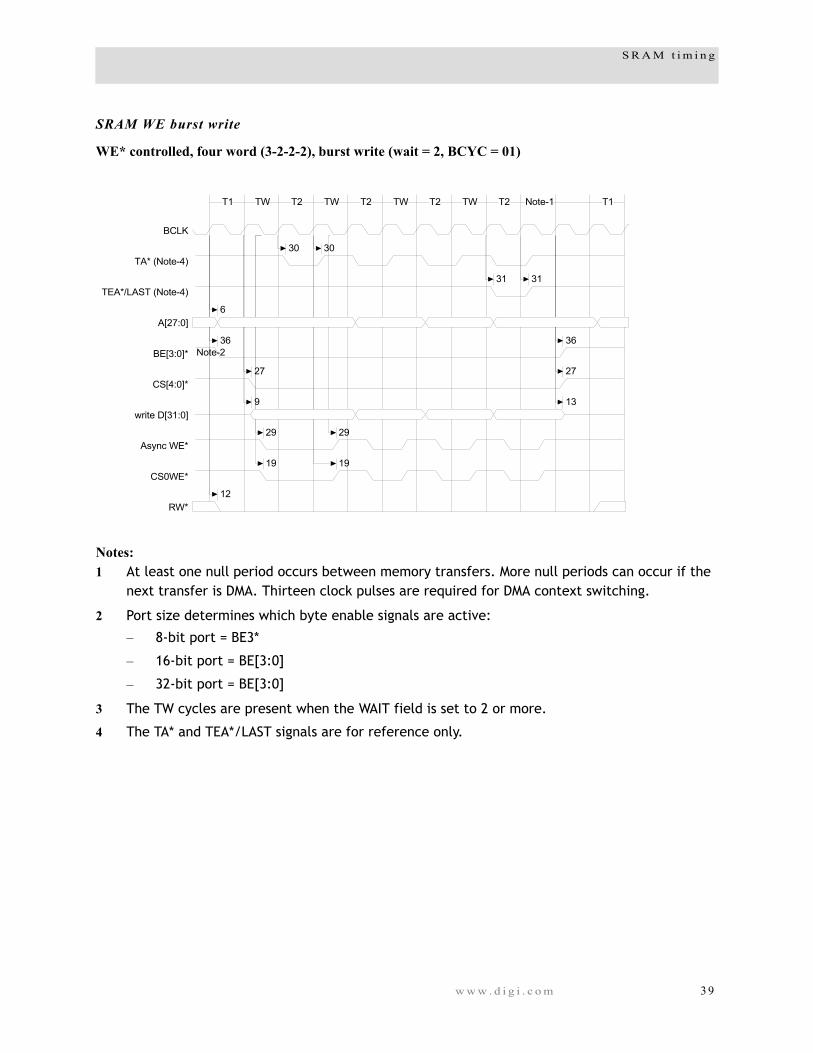
SRAM WE burst write
WE* controlled, four word (3-2-2-2), burst write (wait = 2, BCYC = 01)
Notes:1 At least one null period occurs between memory transfers. More null periods can occur if the
next transfer is DMA. Thirteen clock pulses are required for DMA context switching.
2 Port size determines which byte enable signals are active:
– 8-bit port = BE3*
– 16-bit port = BE[3:0]
– 32-bit port = BE[3:0]
3 The TW cycles are present when the WAIT field is set to 2 or more.
4 The TA* and TEA*/LAST signals are for reference only.
T1 TW T2 TW T2 TW T2 TW T2 Note-1 T1
12
1919
2929
139
2727
3636
6
3131
3030
Note-2
BCLK
TA* (Note-4)
TEA*/LAST (Note-4)
A[27:0]
BE[3:0]*
CS[4:0]*
write D[31:0]
Async WE*
CS0WE*
RW*
w w w . d i g i . c o m 3 9
S D R A M t i m i n g
SDRAM timing BCLK max frequency: 55.296 MHz
Operating conditions:
SDRAM timing parameters
Temperature: -15.00 (min) 110.00 (max)
Voltage: 1.60 (min) 1.40 (max)
Output load: 25.0pf
Input drive: CMOS buffer
Num Description Min Max Unit
36 BCLK high to BE*/DQM* valid 15.5 ns
6 BCLK high to non-muxed address valid 5 13.5 ns
9 BCLK high to data out valid 14 ns
13 BCLK high to data out high impedance 13 ns
10 Data in valid to BCLK high (setup) 5 ns
11 BCLK high to data in invalid (hold) 3 ns
27 BCLK high to CS* valid 15.5 ns
30 BCLK high to TA* valid 13.5 ns
31 BCLK high to TEA* valid 16 ns
37 BCLK high to PORTA2/AMUX valid 14 ns
35 BCLK high to muxed address valid 6 14.5 ns
34 BCLK high to CAS* valid 12 ns
12 BCLK high to RW* valid 13.5 ns
4 0 N S 7 5 2 0 D a t a s h e e t R e v . E 1 0 / 2 0 0 7
S D R A M t i m i n g
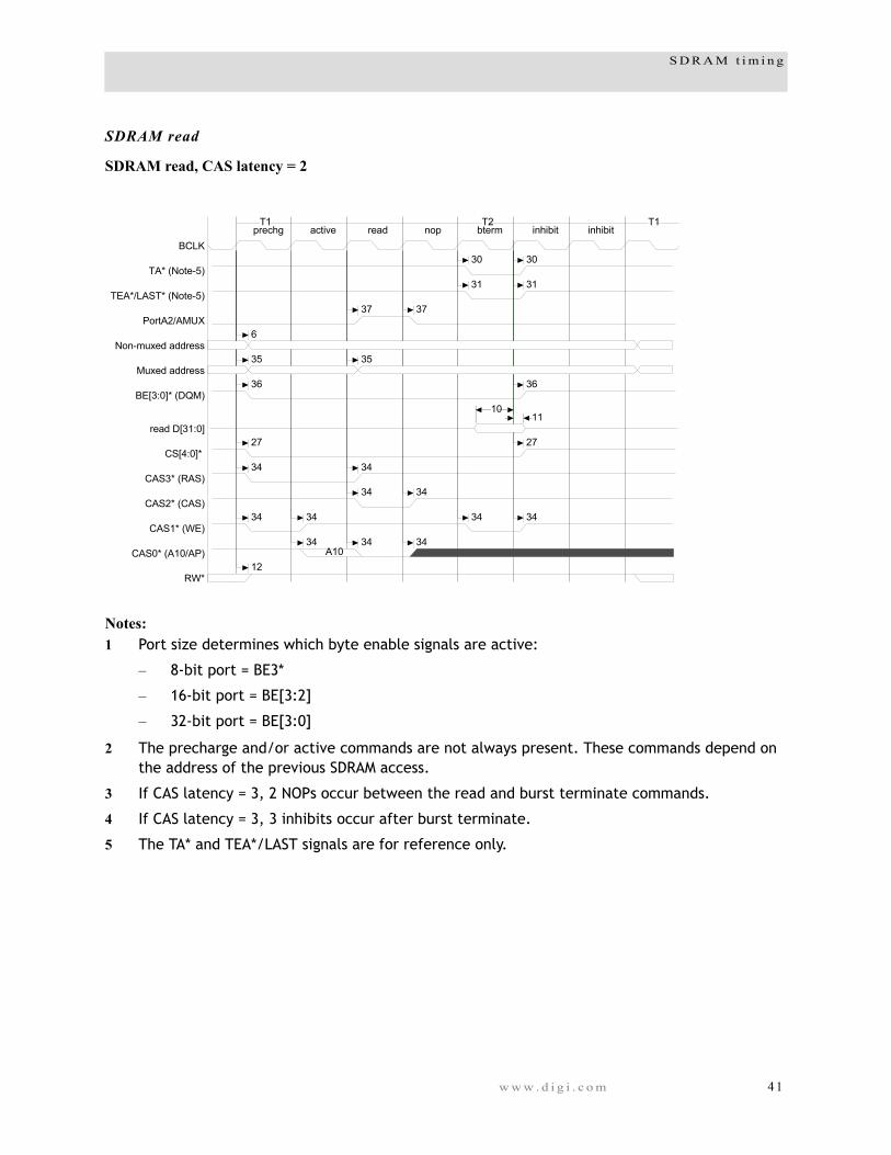
SDRAM read
SDRAM read, CAS latency = 2
Notes:1 Port size determines which byte enable signals are active:
– 8-bit port = BE3*
– 16-bit port = BE[3:2]
– 32-bit port = BE[3:0]
2 The precharge and/or active commands are not always present. These commands depend on the address of the previous SDRAM access.
3 If CAS latency = 3, 2 NOPs occur between the read and burst terminate commands.
4 If CAS latency = 3, 3 inhibits occur after burst terminate.
5 The TA* and TEA*/LAST signals are for reference only.
T1 T2 T1prechg active read nop bterm inhibit inhibit
12
343434
34343434
3434
3434
2727
3636
3535
6
3737
3131
3030
1110
A10
BCLK
TA* (Note-5)
TEA*/LAST* (Note-5)
PortA2/AMUX
Non-muxed address
Muxed address
BE[3:0]* (DQM)
read D[31:0]
CS[4:0]*
CAS3* (RAS)
CAS2* (CAS)
CAS1* (WE)
CAS0* (A10/AP)
RW*
w w w . d i g i . c o m 4 1
S D R A M t i m i n g
SDRAM burst read
SDRAM read, CAS latency = 2
Notes:1 Port size determines which byte enable signals are active:
– 8-bit port = BE3*
– 16-bit port = BE[3:2]
– 32-bit port = BE[3:0]
2 The precharge and/or active commands are not always present. These commands depend on the address of the previous SDRAM access.
3 If CAS latency = 3, 5 NOPs occur between the read and burst terminate commands.
4 If CAS latency = 3, 3 inhibits occur after burst terminate.
5 The TA* and TEA*/LAST signals are for reference only.
T1 T2 T2 T2 T2 T1prechg active read nop nop nop nop bterm inhibit inhibit
12
343434
34343434
3434
3434
2727
3636
3535
6
3737
3131
3030
1110
A10
BCLK
TA* (Note-5)
TEA*/LAST* (Note-5)
PortA2/AMUX
Non-muxed address
Muxed address
BE*[3:0]* (DQM)
read D[31:0]
CS[4:0]*
CAS3* (RAS)
CAS2* (CAS)
CAS1* (WE)
CAS0* (A10/AP)
RW*
4 2 N S 7 5 2 0 D a t a s h e e t R e v . E 1 0 / 2 0 0 7
S D R A M t i m i n g
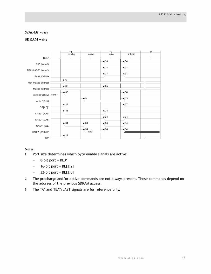
SDRAM write
SDRAM write
Notes:1 Port size determines which byte enable signals are active:
– 8-bit port = BE3*
– 16-bit port = BE[3:2]
– 32-bit port = BE[3:0]
2 The precharge and/or active commands are not always present. These commands depend on the address of the previous SDRAM access.
3 The TA* and TEA*/LAST signals are for reference only.
T1 T2 T1prechg active write inhibit
12
343434
34343434
3434
3434
2727
139
3636
3535
6
3737
3131
3030
A10
Note-1
BCLK
TA* (Note-3)
TEA*/LAST* (Note-3)
PortA2/AMUX
Non-muxed address
Muxed address
BE[3:0]* (DQM)
write D[31:0]
CS[4:0]*
CAS3* (RAS)
CAS2* (CAS)
CAS1* (WE)
CAS0* (A10/AP)
RW*
w w w . d i g i . c o m 4 3
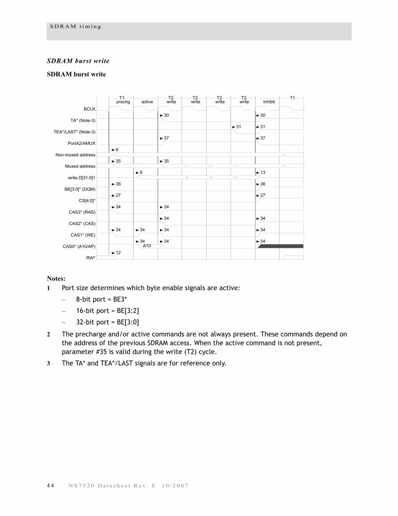
S D R A M t i m i n g
SDRAM burst write
SDRAM burst write
Notes:1 Port size determines which byte enable signals are active:
– 8-bit port = BE3*
– 16-bit port = BE[3:2]
– 32-bit port = BE[3:0]
2 The precharge and/or active commands are not always present. These commands depend on the address of the previous SDRAM access. When the active command is not present, parameter #35 is valid during the write (T2) cycle.
3 The TA* and TEA*/LAST signals are for reference only.
T1 T2 T2 T2 T2 T1prechg active write write write write inhibit
12
343434
34343434
3434
3434
2727
3636
139
3535
6
3737
3131
3030
A10
BCLK
TA* (Note-3)
TEA*/LAST* (Note-3)
PortA2/AMUX
Non-muxed address
Muxed address
write D[31:0]1
BE[3:0]* (DQM)
CS[4:0]*
CAS3* (RAS)
CAS2* (CAS)
CAS1* (WE)
CAS0* (A10/AP)
RW*
4 4 N S 7 5 2 0 D a t a s h e e t R e v . E 1 0 / 2 0 0 7
S D R A M t i m i n g
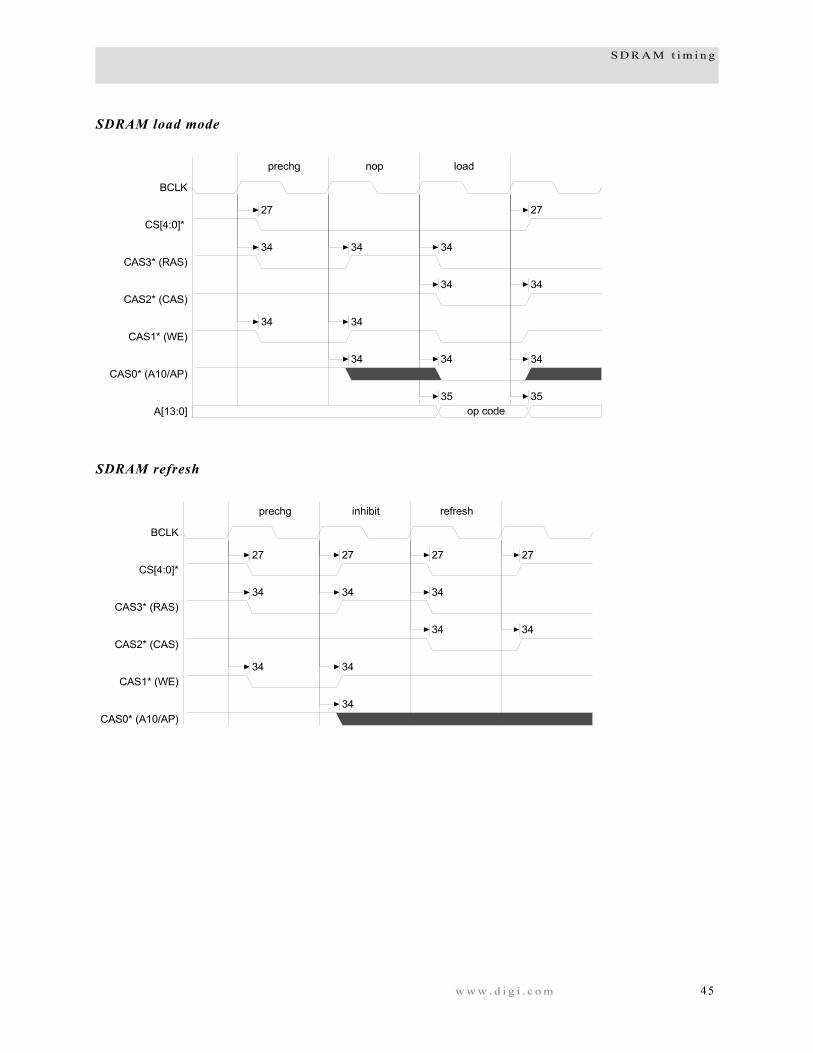
SDRAM load mode
SDRAM refresh
prechg nop load
3535
343434
3434
3434
343434
2727
op code
BCLK
CS[4:0]*
CAS3* (RAS)
CAS2* (CAS)
CAS1* (WE)
CAS0* (A10/AP)
A[13:0]
prechg inhibit refresh
34
3434
3434
343434
27272727
BCLK
CS[4:0]*
CAS3* (RAS)
CAS2* (CAS)
CAS1* (WE)
CAS0* (A10/AP)
w w w . d i g i . c o m 4 5
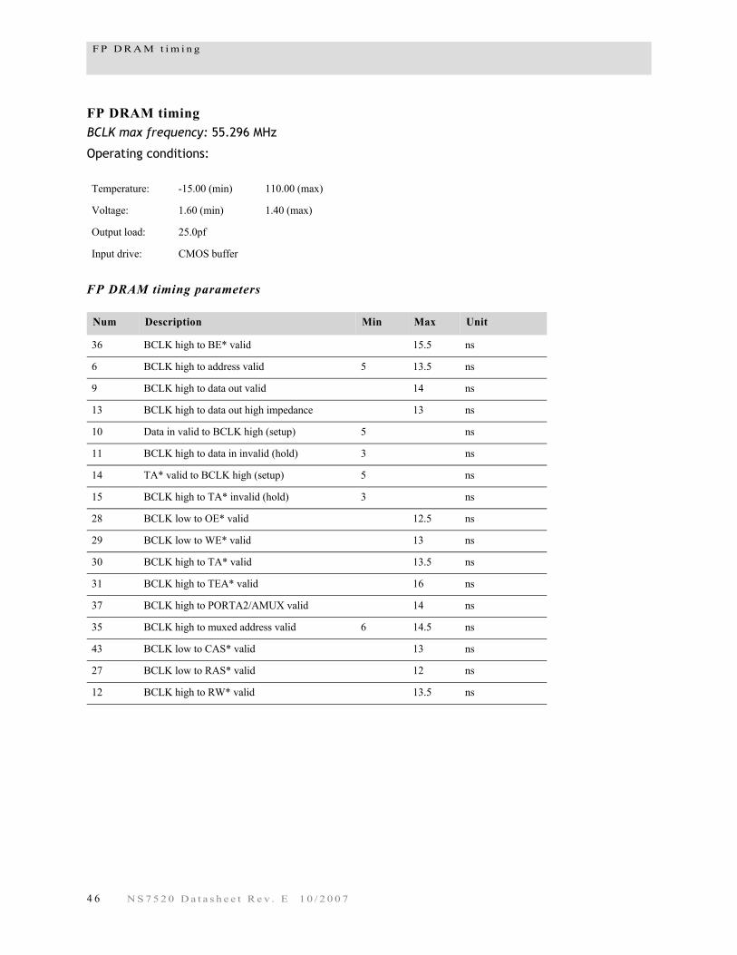
F P D R A M t i m i n g
FP DRAM timingBCLK max frequency: 55.296 MHz
Operating conditions:
FP DRAM timing parameters
Temperature: -15.00 (min) 110.00 (max)
Voltage: 1.60 (min) 1.40 (max)
Output load: 25.0pf
Input drive: CMOS buffer
Num Description Min Max Unit
36 BCLK high to BE* valid 15.5 ns
6 BCLK high to address valid 5 13.5 ns
9 BCLK high to data out valid 14 ns
13 BCLK high to data out high impedance 13 ns
10 Data in valid to BCLK high (setup) 5 ns
11 BCLK high to data in invalid (hold) 3 ns
14 TA* valid to BCLK high (setup) 5 ns
15 BCLK high to TA* invalid (hold) 3 ns
28 BCLK low to OE* valid 12.5 ns
29 BCLK low to WE* valid 13 ns
30 BCLK high to TA* valid 13.5 ns
31 BCLK high to TEA* valid 16 ns
37 BCLK high to PORTA2/AMUX valid 14 ns
35 BCLK high to muxed address valid 6 14.5 ns
43 BCLK low to CAS* valid 13 ns
27 BCLK low to RAS* valid 12 ns
12 BCLK high to RW* valid 13.5 ns
4 6 N S 7 5 2 0 D a t a s h e e t R e v . E 1 0 / 2 0 0 7
F P D R A M t i m i n g
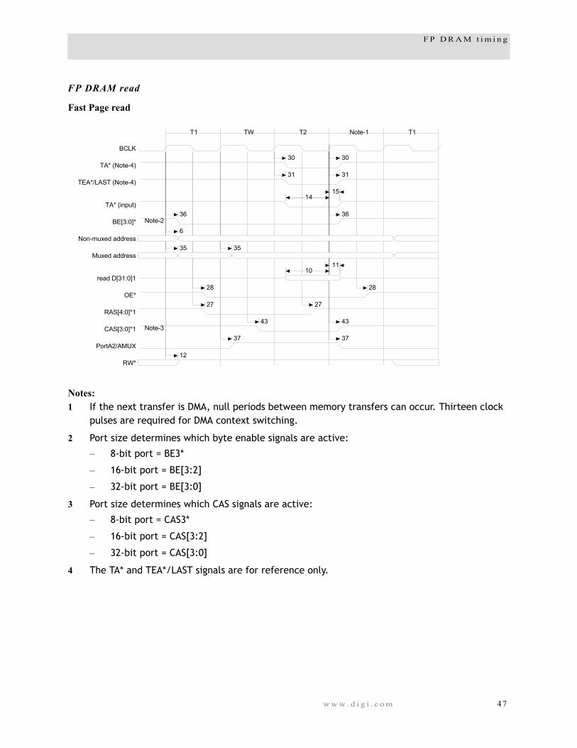
FP DRAM read
Fast Page read
Notes:1 If the next transfer is DMA, null periods between memory transfers can occur. Thirteen clock
pulses are required for DMA context switching.
2 Port size determines which byte enable signals are active:
– 8-bit port = BE3*
– 16-bit port = BE[3:2]
– 32-bit port = BE[3:0]
3 Port size determines which CAS signals are active:
– 8-bit port = CAS3*
– 16-bit port = CAS[3:2]
– 32-bit port = CAS[3:0]
4 The TA* and TEA*/LAST signals are for reference only.
T1 TW T2 Note-1 T1
12
3737
4343
2727
2828
3535
6
3636
3131
3030
1110
1514
Note-2
Note-3
BCLK
TA* (Note-4)
TEA*/LAST (Note-4)
TA* (input)
BE[3:0]*
Non-muxed address
Muxed address
read D[31:0]1
OE*
RAS[4:0]*1
CAS[3:0]*1
PortA2/AMUX
RW*
w w w . d i g i . c o m 4 7
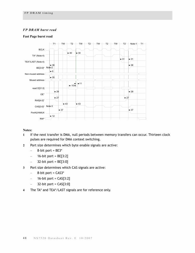
F P D R A M t i m i n g
FP DRAM burst read
Fast Page burst read
Notes:1 If the next transfer is DMA, null periods between memory transfers can occur. Thirteen clock
pulses are required for DMA context switching.
2 Port size determines which byte enable signals are active:
– 8-bit port = BE3*
– 16-bit port = BE[3:2]
– 32-bit port = BE[3:0]
3 Port size determines which CAS signals are active:
– 8-bit port = CAS3*
– 16-bit port = CAS[3:2]
– 32-bit port = CAS[3:0]
4 The TA* and TEA*/LAST signals are for reference only.
T1 TW T2 TW T2 TW T2 TW T2 Note-1 T1
12
3737
4343
2727
2828
35
6
3636
3131
3030
1110
Note-2
Note-3
BCLK
TA* (Note-4)
TEA*/LAST (Note-4)
BE[3:0]*
Non-muxed address
Muxed address
read D[31:0]
OE*
RAS[4:0]*
CAS[3:0]*
PortA2/AMUX
RW*
4 8 N S 7 5 2 0 D a t a s h e e t R e v . E 1 0 / 2 0 0 7
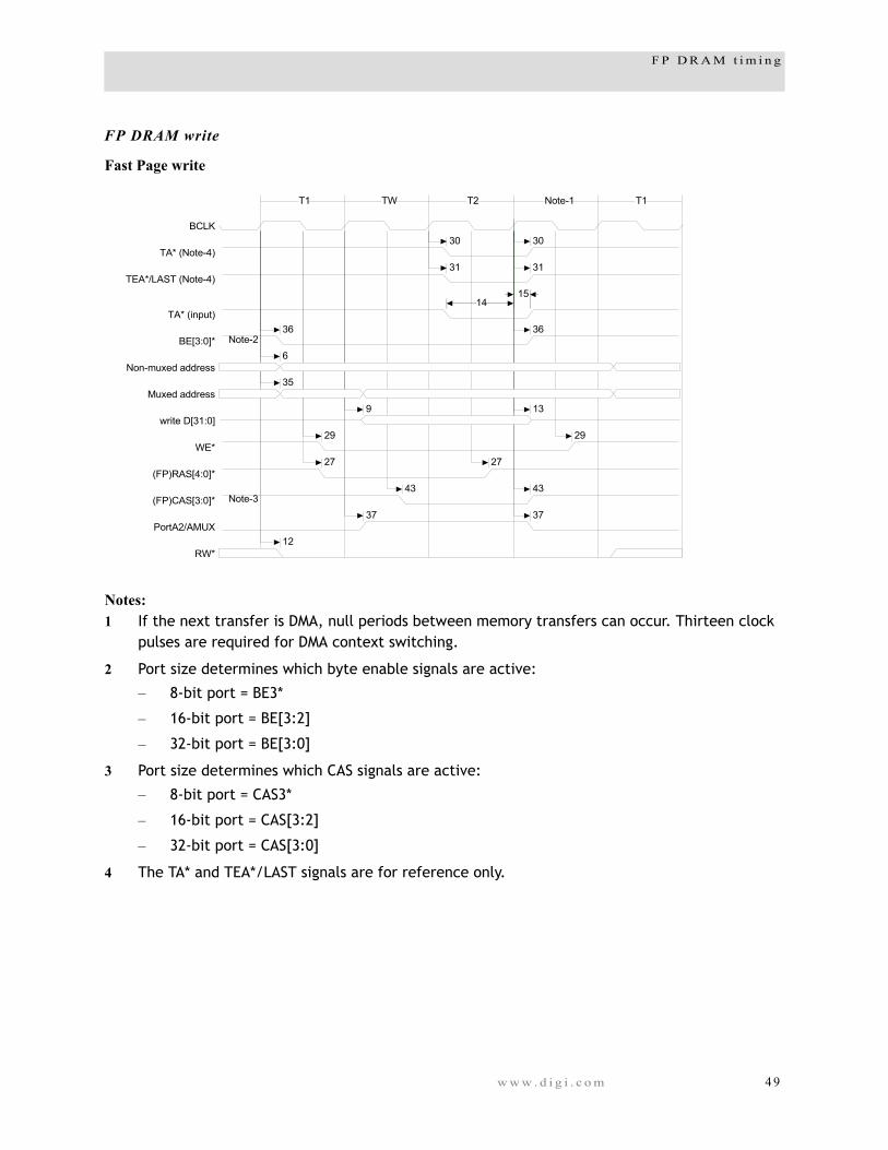
F P D R A M t i m i n g
FP DRAM write
Fast Page write
Notes:1 If the next transfer is DMA, null periods between memory transfers can occur. Thirteen clock
pulses are required for DMA context switching.
2 Port size determines which byte enable signals are active:
– 8-bit port = BE3*
– 16-bit port = BE[3:2]
– 32-bit port = BE[3:0]
3 Port size determines which CAS signals are active:
– 8-bit port = CAS3*
– 16-bit port = CAS[3:2]
– 32-bit port = CAS[3:0]
4 The TA* and TEA*/LAST signals are for reference only.
T1 TW T2 Note-1 T1
12
3737
4343
2727
2929
139
35
6
3636
3131
3030
1514
Note-2
Note-3
BCLK
TA* (Note-4)
TEA*/LAST (Note-4)
TA* (input)
BE[3:0]*
Non-muxed address
Muxed address
write D[31:0]
WE*
(FP)RAS[4:0]*
(FP)CAS[3:0]*
PortA2/AMUX
RW*
w w w . d i g i . c o m 4 9
F P D R A M t i m i n g
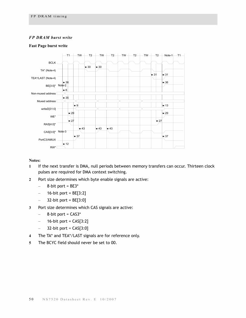
FP DRAM burst write
Fast Page burst write
Notes:1 If the next transfer is DMA, null periods between memory transfers can occur. Thirteen clock
pulses are required for DMA context switching.
2 Port size determines which byte enable signals are active:
– 8-bit port = BE3*
– 16-bit port = BE[3:2]
– 32-bit port = BE[3:0]
3 Port size determines which CAS signals are active:
– 8-bit port = CAS3*
– 16-bit port = CAS[3:2]
– 32-bit port = CAS[3:0]
4 The TA* and TEA*/LAST signals are for reference only.
5 The BCYC field should never be set to 00.
T1 TW T2 TW T2 TW T2 TW T2 Note-1 T1
12
3737
434343
2727
2929
139
35
6
3636
3131
3030
Note-2
Note-3
BCLK
TA* (Note-4)
TEA*/LAST (Note-4)
BE[3:0]*
Non-muxed address
Muxed address
writeD[31:0]
WE*
RAS[4:0]*
CAS[3:0]*
PortC3/AMUX
RW*
5 0 N S 7 5 2 0 D a t a s h e e t R e v . E 1 0 / 2 0 0 7
F P D R A M t i m i n g
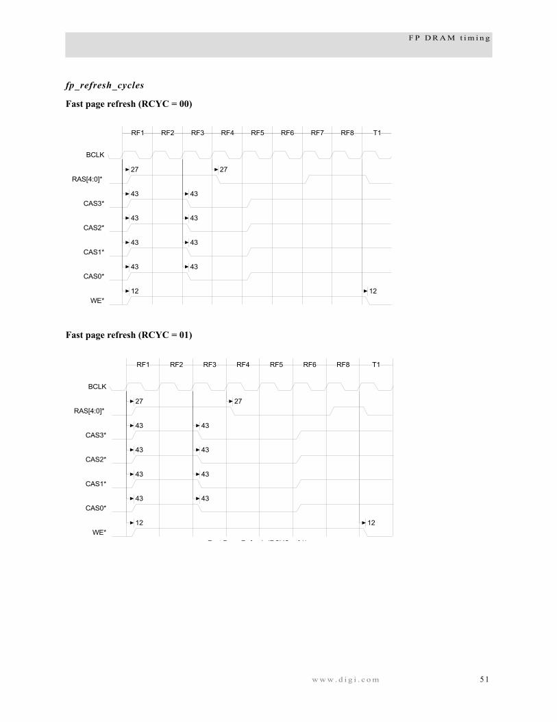
fp_refresh_cycles
Fast page refresh (RCYC = 00)
Fast page refresh (RCYC = 01)
RF1 RF2 RF3 RF4 RF5 RF6 RF7 RF8 T1
1212
4343
4343
4343
4343
2727
BCLK
RAS[4:0]*
CAS3*
CAS2*
CAS1*
CAS0*
WE*
RF1 RF2 RF3 RF4 RF5 RF6 RF8 T1
1212
4343
4343
4343
4343
2727
F t P R f h (RCYC 01)
BCLK
RAS[4:0]*
CAS3*
CAS2*
CAS1*
CAS0*
WE*
w w w . d i g i . c o m 5 1
F P D R A M t i m i n g
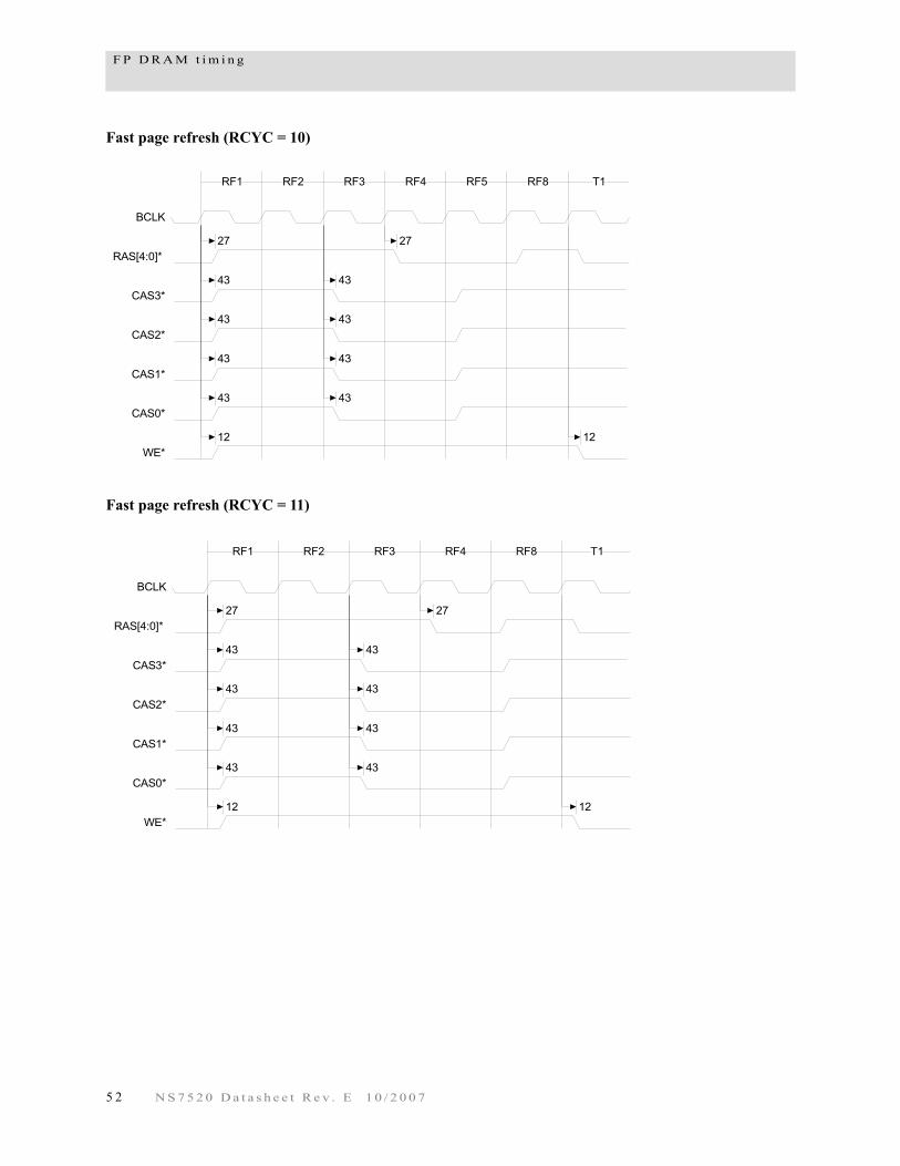
Fast page refresh (RCYC = 10)
Fast page refresh (RCYC = 11)
RF1 RF2 RF3 RF4 RF5 RF8 T1
1212
4343
4343
4343
4343
2727
BCLK
RAS[4:0]*
CAS3*
CAS2*
CAS1*
CAS0*
WE*
RF1 RF2 RF3 RF4 RF8 T1
1212
4343
4343
4343
4343
2727
BCLK
RAS[4:0]*
CAS3*
CAS2*
CAS1*
CAS0*
WE*
5 2 N S 7 5 2 0 D a t a s h e e t R e v . E 1 0 / 2 0 0 7
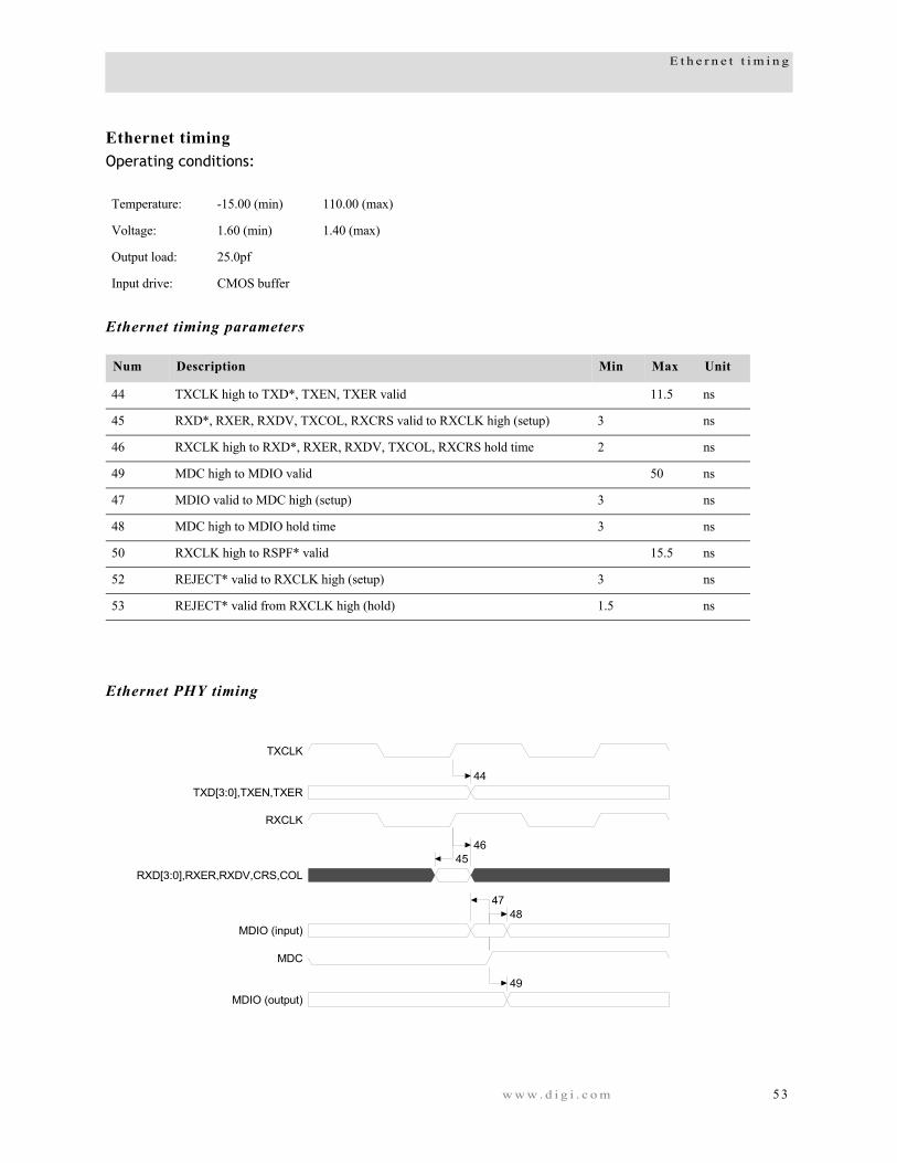
E t h e r n e t t i m i n g
Ethernet timingOperating conditions:
Ethernet timing parameters
Ethernet PHY timing
Temperature: -15.00 (min) 110.00 (max)
Voltage: 1.60 (min) 1.40 (max)
Output load: 25.0pf
Input drive: CMOS buffer
Num Description Min Max Unit
44 TXCLK high to TXD*, TXEN, TXER valid 11.5 ns
45 RXD*, RXER, RXDV, TXCOL, RXCRS valid to RXCLK high (setup) 3 ns
46 RXCLK high to RXD*, RXER, RXDV, TXCOL, RXCRS hold time 2 ns
49 MDC high to MDIO valid 50 ns
47 MDIO valid to MDC high (setup) 3 ns
48 MDC high to MDIO hold time 3 ns
50 RXCLK high to RSPF* valid 15.5 ns
52 REJECT* valid to RXCLK high (setup) 3 ns
53 REJECT* valid from RXCLK high (hold) 1.5 ns
49
4847
4645
44
TXCLK
TXD[3:0],TXEN,TXER
RXCLK
RXD[3:0],RXER,RXDV,CRS,COL
MDIO (input)
MDC
MDIO (output)
w w w . d i g i . c o m 5 3
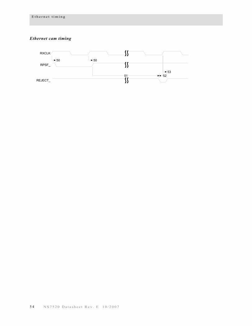
E t h e r n e t t i m i n g
Ethernet cam timing
5351 52
5050
RXCLK
RPSF_
REJECT_
5 4 N S 7 5 2 0 D a t a s h e e t R e v . E 1 0 / 2 0 0 7
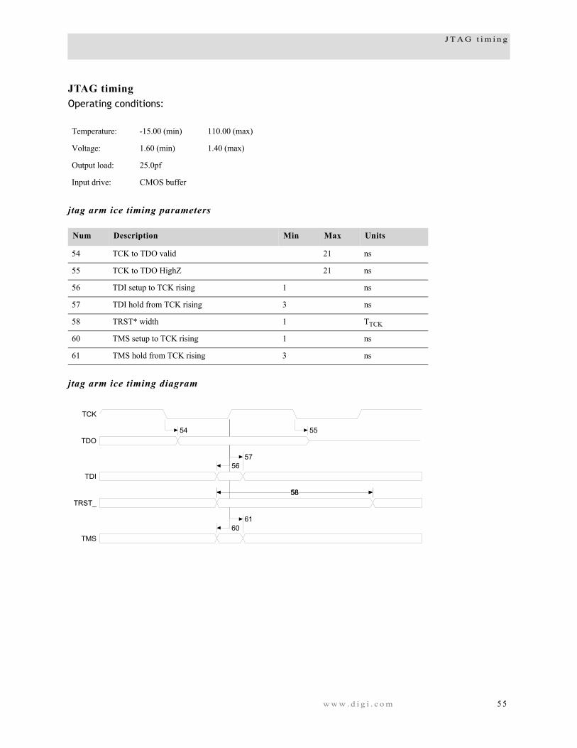
J T A G t i m i n g
JTAG timingOperating conditions:
jtag arm ice timing parameters
jtag arm ice timing diagram
Temperature: -15.00 (min) 110.00 (max)
Voltage: 1.60 (min) 1.40 (max)
Output load: 25.0pf
Input drive: CMOS buffer
Num Description Min Max Units
54 TCK to TDO valid 21 ns
55 TCK to TDO HighZ 21 ns
56 TDI setup to TCK rising 1 ns
57 TDI hold from TCK rising 3 ns
58 TRST* width 1 TTCK
60 TMS setup to TCK rising 1 ns
61 TMS hold from TCK rising 3 ns
6160
5756
5554
5858
TCK
TDO
TDI
TRST_
TMS
w w w . d i g i . c o m 5 5
J T A G t i m i n g
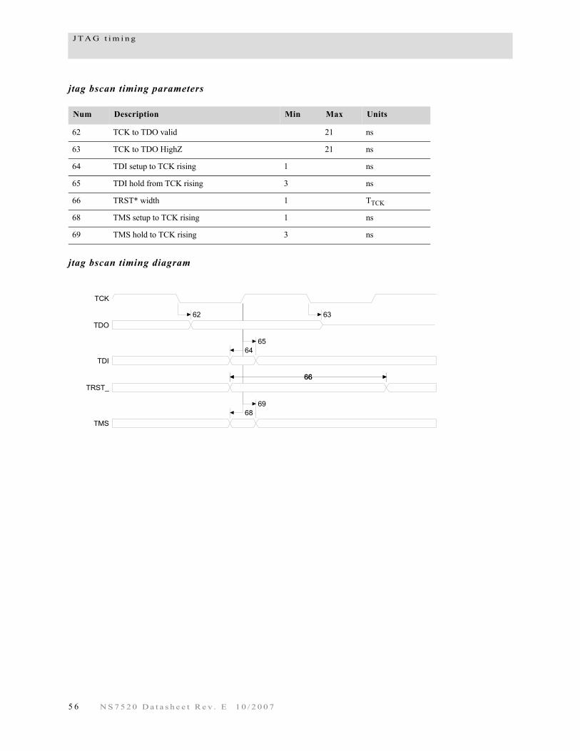
jtag bscan timing parameters
jtag bscan timing diagram
Num Description Min Max Units
62 TCK to TDO valid 21 ns
63 TCK to TDO HighZ 21 ns
64 TDI setup to TCK rising 1 ns
65 TDI hold from TCK rising 3 ns
66 TRST* width 1 TTCK
68 TMS setup to TCK rising 1 ns
69 TMS hold to TCK rising 3 ns
6968
6564
6362
6666
TCK
TDO
TDI
TRST_
TMS
5 6 N S 7 5 2 0 D a t a s h e e t R e v . E 1 0 / 2 0 0 7
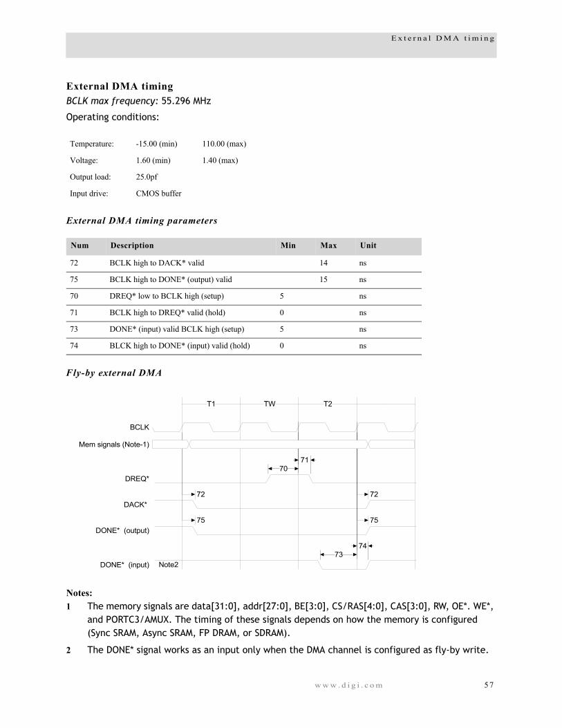
E x t e r n a l D M A t i m i n g
External DMA timingBCLK max frequency: 55.296 MHz
Operating conditions:
External DMA timing parameters
Fly-by external DMA
Notes:1 The memory signals are data[31:0], addr[27:0], BE[3:0], CS/RAS[4:0], CAS[3:0], RW, OE*. WE*,
and PORTC3/AMUX. The timing of these signals depends on how the memory is configured (Sync SRAM, Async SRAM, FP DRAM, or SDRAM).
2 The DONE* signal works as an input only when the DMA channel is configured as fly-by write.
Temperature: -15.00 (min) 110.00 (max)
Voltage: 1.60 (min) 1.40 (max)
Output load: 25.0pf
Input drive: CMOS buffer
Num Description Min Max Unit
72 BCLK high to DACK* valid 14 ns
75 BCLK high to DONE* (output) valid 15 ns
70 DREQ* low to BCLK high (setup) 5 ns
71 BCLK high to DREQ* valid (hold) 0 ns
73 DONE* (input) valid BCLK high (setup) 5 ns
74 BLCK high to DONE* (input) valid (hold) 0 ns
T1 TW T2
7575
7272
7473
7170
Note2
BCLK
Mem signals (Note-1)
DREQ*
DACK*
DONE* (output)
DONE* (input)
w w w . d i g i . c o m 5 7
E x t e r n a l D M A t i m i n g
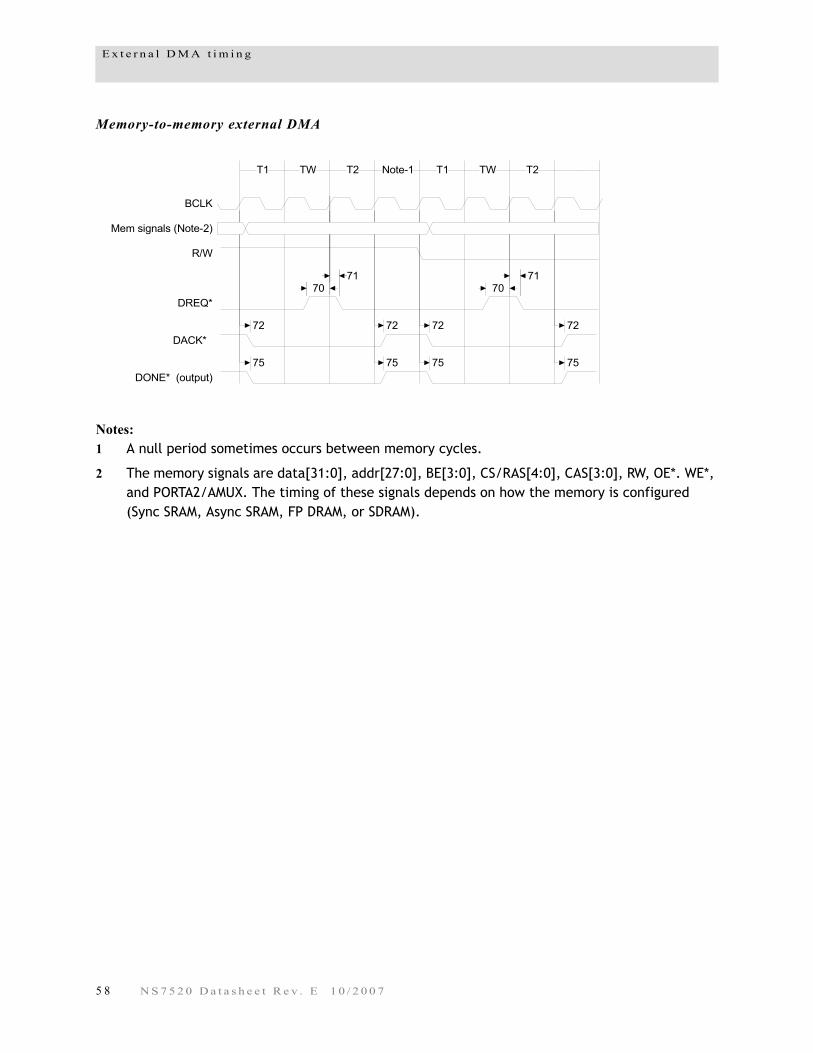
Memory-to-memory external DMA
Notes:1 A null period sometimes occurs between memory cycles.
2 The memory signals are data[31:0], addr[27:0], BE[3:0], CS/RAS[4:0], CAS[3:0], RW, OE*. WE*, and PORTA2/AMUX. The timing of these signals depends on how the memory is configured (Sync SRAM, Async SRAM, FP DRAM, or SDRAM).
T1 TW T2 Note-1 T1 TW T2
75757575
72727272
7170
7170
BCLK
Mem signals (Note-2)
R/W
DREQ*
DACK*
DONE* (output)
5 8 N S 7 5 2 0 D a t a s h e e t R e v . E 1 0 / 2 0 0 7
S e r i a l i n t e r n a l / e x t e r n a l t i m i n g
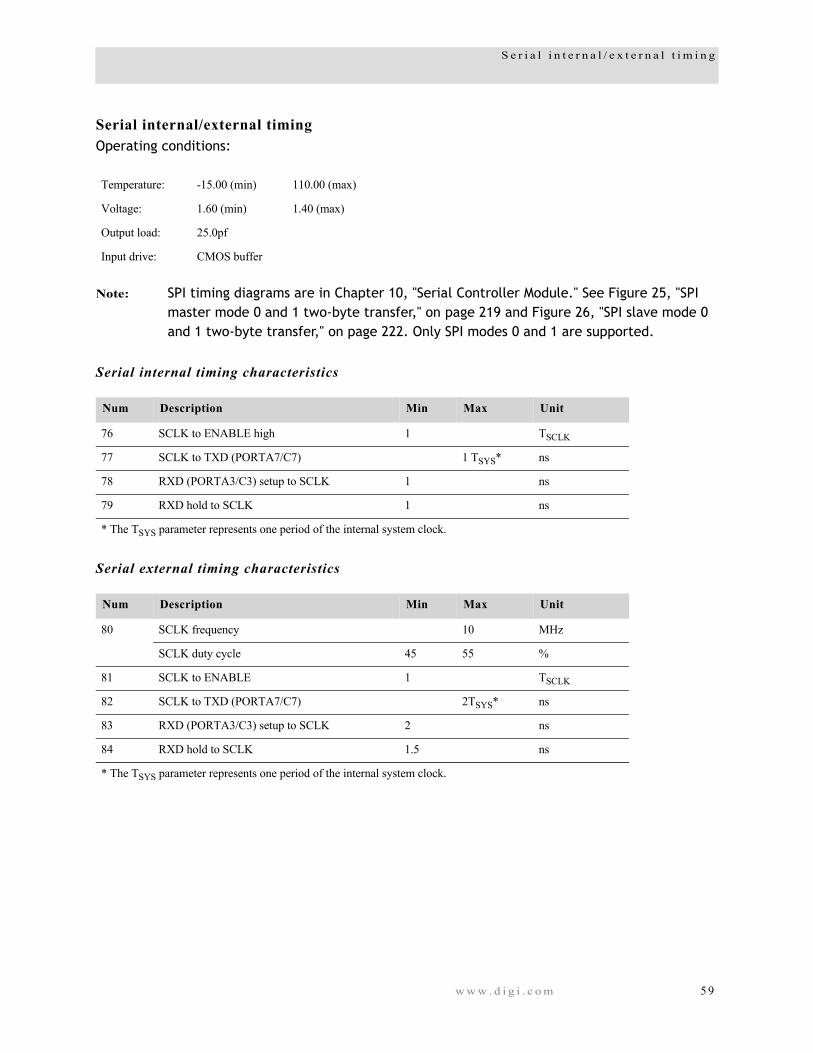
Serial internal/external timingOperating conditions:
Note: SPI timing diagrams are in Chapter 10, "Serial Controller Module." See Figure 25, "SPI master mode 0 and 1 two-byte transfer," on page 219 and Figure 26, "SPI slave mode 0 and 1 two-byte transfer," on page 222. Only SPI modes 0 and 1 are supported.
Serial internal timing characteristics
Serial external timing characteristics
Temperature: -15.00 (min) 110.00 (max)
Voltage: 1.60 (min) 1.40 (max)
Output load: 25.0pf
Input drive: CMOS buffer
Num Description Min Max Unit
76 SCLK to ENABLE high 1 TSCLK
77 SCLK to TXD (PORTA7/C7) 1 TSYS* ns
78 RXD (PORTA3/C3) setup to SCLK 1 ns
79 RXD hold to SCLK 1 ns
* The TSYS parameter represents one period of the internal system clock.
Num Description Min Max Unit
80 SCLK frequency 10 MHz
SCLK duty cycle 45 55 %
81 SCLK to ENABLE 1 TSCLK
82 SCLK to TXD (PORTA7/C7) 2TSYS* ns
83 RXD (PORTA3/C3) setup to SCLK 2 ns
84 RXD hold to SCLK 1.5 ns
* The TSYS parameter represents one period of the internal system clock.
w w w . d i g i . c o m 5 9
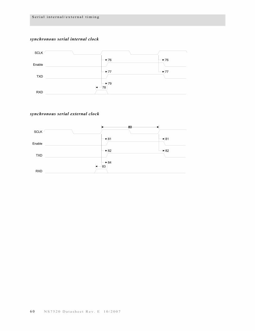
S e r i a l i n t e r n a l / e x t e r n a l t i m i n g
synchronous serial internal clock
synchronous serial external clock
7978
7777
7676
SCLK
Enable
TXD
RXD
8483
8282
8181
8080SCLK
Enable
TXD
RXD
6 0 N S 7 5 2 0 D a t a s h e e t R e v . E 1 0 / 2 0 0 7
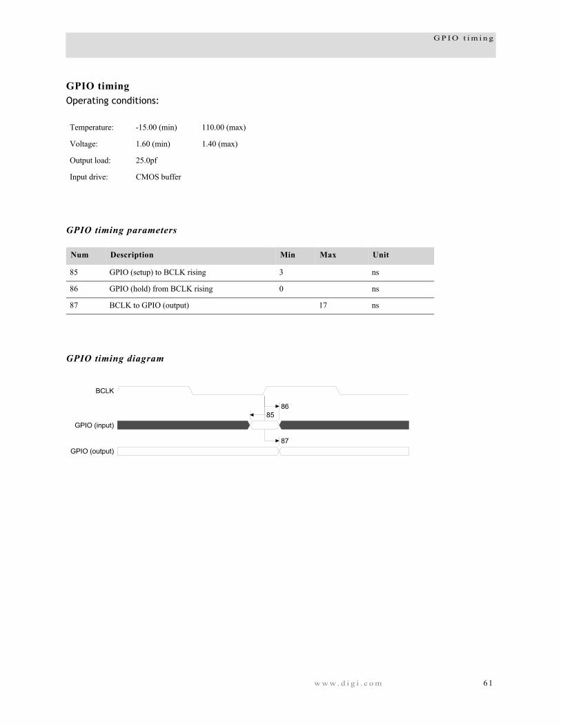
G P I O t i m i n g
GPIO timingOperating conditions:
GPIO timing parameters
GPIO timing diagram
Temperature: -15.00 (min) 110.00 (max)
Voltage: 1.60 (min) 1.40 (max)
Output load: 25.0pf
Input drive: CMOS buffer
Num Description Min Max Unit
85 GPIO (setup) to BCLK rising 3 ns
86 GPIO (hold) from BCLK rising 0 ns
87 BCLK to GPIO (output) 17 ns
87
8685
BCLK
GPIO (input)
GPIO (output)
w w w . d i g i . c o m 6 1
G P I O t i m i n g
P/N: 90000303_E
© Digi International Inc. 2005-2007 All rights reserved.
Digi, Digi International, the Digi logo, the Making Device Networking Easy logo, NetSilicon, a Digi International Company, NET+, NET+OS and NET+Works are trademarks or registered trademarks of Digi International, Inc. in the United States and other countries worldwide. All other trademarks are the property of their respective owners.
Information in this document is subject to change without notice and does not represent a committment on the part of Digi International.
Digi provides this document “as is,” without warranty of any kind, either expressed or implied, including, but not limited to, the implied warranties of, fitness or merchantability for a particular purpose. Digi may make improvements and/or changes in this manual or in the product(s) and/or the program(s) described in this manual at any time.
This product could include technical inaccuracies or typographical errors. Changes are made periodically to the information herein; these changes may be incorporated in new editions of the publication.
6 2 N S 7 5 2 0 D a t a s h e e t R e v . E 1 0 / 2 0 0 7

G P I O t i m i n g
w w w . d i g i . c o m 6 3

Digi International11001 Bren Road EastMinnetonka, MN 55343 U.S.A.United States: +1 877 912-3444Other locations: +1 952 912-3444Fax: +1 952 912-4960www.digiembedded.com