november 1984 procedures for precap visual inspection · november 1984 procedures for precap ......
TRANSCRIPT
NASA Reference Publication 1122
November 1984 Procedures for Precap Visual Inspection
-; -i
https://ntrs.nasa.gov/search.jsp?R=19850004848 2018-06-10T02:14:24+00:00Z
TECH LIBRARY KAFB. NM
NASA Reference Publication 1122
1984
Natlonal Aeronautics and Space AdmInIstration
Scientific and Technical Information Branch
0063L7b
Procedures for Precap Visual Inspection
Oflice of the Chief Engineer National Aeronautics and Space Administration Washington, D.C.
Library of Congress Cataloging in Publication Data Main entry under title: Procedures for precap visual inspection.
(NASA Reference Publication ; 1122) Bibliography: p. 75 1. Integrated circuits-Inspection I. United States.
National Aeronautics and Space Administration. Scientific and Technical Information Branch. II. Series. TK7874.P74 1984 621.381’.73’0287 84-16628
FOREWORD
This document describes the techniques that can be employed for the final precap visual inspection of micro- circuits used in electronic system components. It can also serve as an effective tool in training personnel to per- form these tasks in an efficient and reliable manner.
To aid in the training of personnel unfamiliar with microcircuits, the first chapter includes a brief description of the processing techniques that are commonly used in industry for the manufacture of monolithic and hybrid components.
Subsequent sections describe the imperfections that may be encountered in the precap visual inspection of these semiconductor components. Photomicrographs are used to illustrate problem areas, such as scratches, voids, adhesions, bridging of the metallization, corrosion of the aluminum, misalignment, and wire bonding faults. Acceptance and rejection criteria are established for many defects.
The information contained herein may be used for the guidance of NASA personnel. It is distributed to other government agencies and contractors as a courtesy. Although portions of it may be altered, revised, or rescinded, depending on new developments, these changes may not be imparted directly to the holders of this document, but may be provided instead to NASA personnel by means of memoranda or other correspondence through limited channels. Users of this document should therefore keep abreast of the state of the art of precap visual inspection.
Neither the United States Government nor any personnel acting on behalf of the United States Government assumes any liability for the use of this document.
MILTON A. SILVERA Chief Engineer
. . . ln
Ii. ---_-. -_

CONTENTS
Page
GLOSSARY ............................................................ vii
INTRODUCTION ......................................................... 1
INTEGRATED CIRCUIT PROCESSING. ......................................... 2
Monolithic Circuits .................................................... 2
Fabrication ..................................................... 2 Packaging ....................................................... 8
HybridCircuits ....................................................... 11
MONOLITHIC CIRCUIT DEFECTS. ............................................ 15
Die ............................................................... 15
Metallization .................................................... 15 Diffusion, Passivation, and Dielectric Isolation .............................. 21 Glassivation ..................................................... 28 Sc~bing ........................................................ 33 Thin-Film Resistors. ............................................... 33
W~eBonding ........................................................ 41
InternalPackaging ..................................................... 52
ForeignMaterial .................................................. 52 DieBonding ..................................................... 57
HYBRIDCIRCUITDEFECTS ................................................. 64
Substrate ........................................................... 64 Substrate Element Assembly .............................................. 65 WireBonding ........................................................ 65 PassiveElements ...................................................... 70 Package Conditions .................................................... 7 1
PRECAPSCENARTO ....................................................... 71
SUMMARY ............................................................. 73
ACKNOWLEDGMENT ...................................................... 73
REFERENCES ........................................................... 75
BIBLIOGRAPHY.. ....................................................... 75
V

GLOSSARY
Bimetallic-Metallurgical system consisting of two different metals.
Chip-Piece of a silicon wafer in which a transistor, or an entire integrated circuit, is contained.
Contact window-Opening etched in the silicon oxide layer to allow ohmic contact to the underlying silicon.
Dice-(v) To break a silicon wafer into individual pieces; (n) pieces of silicon wafer (plural of die-see die).
Die-Singular of dice-individual piece of silicon wafer in which a transistor, or a whole integrated circuit, is contained (see chip).
Epitaxial growth (epitaxyjProcess by which single-crystal material is grown on top of another single crystal.
Eutectic temperature-Lowest temperature at which a two-element metal system can melt.
Evaporation (vapor deposition jMethod of depositing one material on top of another. Atoms of the first ma- terial are boiled off a heated filament and deposited on the second material. The process is carried out in a vacuum.
Interference color-Color that appears in thin films as a result of destructive interference of the light waves as they are transmitted through the film and reflected back from the substrate.
Laminar flow hood-Hood in which airflow in the work area is uniform in its flow pattern and which is relatively free of back-streaming contamination.
Photosensitivity-Property of a material whereby its chemical makeup is altered by exposure to light.
Mil-Unit of measure equal to 0.001 inch.
Passivation layer-Layer of silicon dioxide that is grown on the die surface to act as an insulating medium.
Scribing-Process in which a sharp diamond stylus is moved along a single-crystal silicon wafer, creating stresses in the crystal lattice.
Scrubbing-Process used during soldering in which one of the parts is rapidly moved across the other. The rub- bing motion breaks up oxide formations.
Wafer-Slice of semiconductor material.
vii

INTRODUCTION
The need for highly reliable electronic components has become a critical factor in electronic systems as the demands and complexity of these systems have increased. This is true for both space missions and the consumer market. Consumers have come to expect reliable electronic systems. The same is true for spacecraft designers. However, spacecraft differ in four areas:
They are exposed to a unique environment.
After they are launched, unmanned orbiters cannot be repaired (until shuttle-based repair missions become a reality).
Production is limited to one or at most a few models, increasing the total production cost.
A high rate of success is essential for some or all of the following reasons: budget constraints, national defense, and the dependence of human lives on the information supplied by spacecraft.
In addition, these requirements have become even more stringent with the advent of longer missions and reusable spacecraft such as the shuttle.
The reliability of an electronic system depends entirely on the reliability (along with good circuit design) of the electronic components that make up the system. Once the concern of specialists, quality is becoming central to production. The detection of errors is being shifted from fmal inspection to production and pre- production phases all the way to top management. Original equipment manufacturers (OEM) once ac- cepted good and bad parts from vendors and per- formed their own testing to weed out bad parts-a costly procedure. More and more original equipment manufacturers are recognizing the need for working with vendors to produce good parts in the beginning of manufacturing to ensure that incoming components meet quality assurance levels without the need for extensive screening. Until this level of assurance is met, most users of high-reliability parts will continue to specify elaborate screening procedures. These addi-
tional screens have increased the cost to three or four times that of off-the-shelf components. The screening procedures are effective in removing many parts with built-m manufacturing defects due to deficiency in workmanship or design. However, a significant num- ber of such parts escape these screens.
Failure analyses conducted at Goddard Space Flight Center (GSFC) have shown that a large percentage of microcircuit failures caused by manufacturing defects are attributable to poor workmanship. An important method of detecting workmanship problems is the final precap visual inspection performed during the last step in fabrication before sealing the device with- in its package. In this inspection, each microcircuit is examined (100 percent inspection) at various magnifi- cations and viewing angles.
Experience has shown that manufacturers do not re- move all devices that show poor workmanship. It is therefore inevitable that some of the devices find their way into high-reliability procurements. There are several reasons for the inefficient removal of questionable devices:
l Despite screening standards (for example, MIL- STD-883B), the vendor and user do not com- pletely agree on what constitutes a visual reject.
l Because of the complexity of the parts and often the specification, accept/reject criteria may be misinterpreted.
l The inspector at the final precap visual station examines many devices and may become care- less.
l The inspector is not always aware of the serious- ness of evident imperfections and/or does not ask for clarification when uncertain.
l At times, standards are relaxed (with and with- out approval) for hard-to-produce state-of-the- art devices.
As a result, users of extremely high-reliability material often perform their own final precap visual inspection
1
in addition to or rather than the normal vendor in- spection. This makes it necessary for procuring agen- cies to have personnel who are experienced and trained in the complexities of semiconductor fabrica- tion and inspection. Unfortunately, there are not enough qualified personnel to perform visual exam- inations with a high degree of competence. To alleviate this problem, this document has been prepared to aid in instructing personnel in the art and science of visual inspection.
The material in this document closely follows that of MIL-STD-883B, Methods 2010 and 2017, condition A (class S). Users of class B components should con- sult Methods 2010 and 2017, condition B, for details. Although most of the text concentrates on micro- circuits, the techniques apply to the visual inspection of a variety of electronic components. The text is divided into two major parts. The first part discusses integrated circuit processing of both monolithic and hybrid devices for personnel who are unfamiliar with integrated circuits. The second part discusses defects that can be found in both monolithic and hybrid circuits. The major emphasis is on monolithic device defects. The discussion of hybrids is concerned with areas of fabrication unique to hybrid circuits.
INTEGRATED CIRCUIT PROCESSING
Monolithic Circuits
Fabrication
TWO basic types of electronic components can be fabricated with integrated circuit technology: bi- polar and umpolar. These two designations refer to the type of charge carrier present in the device. In a bipolar device, there are two charge carriers of op- posite polarity; in a unipolar device, there is only one charge carrier. Bipolar devices are generally classified by their circuit type: transistor, transistor logic (T2L), emitter coupled logic (ECL), integrated injec- tion logic (I’L), or diode-transistor logic (DTL). Unipolar devices are classified on the basis of conduc- tivity type (p-channel or n-channel), as well as other processing variations. Unipolar devices are commonly referred to as either field effect transistors (FET) or metal oxide semiconductors (MOS).
A bipolar integrated circuit is made by combining different types of bipolar components on a silicon
chip (fig. 1). Similarly, various MOS components are integrated to form an MOS integrated circuit. Recent advances in semiconductor technology have permit- ted both MOS and bipolar components to be fabri- cated in a single integrated circuit chip.
The number of logic components, usually referred to as gates, on an integrated circuit chip defines the complexity of the device. One to ten gates are referred to as small-scale integration (SSI). Ten to one hun- dred gates are referred to as medium-scale integration (MSI). Large-scale integration (LSI) corresponds to 100 to 1000 gates on one integrated circuit chip. Each very-large-scale integration (VLSI) chip con- tains from 1000 to 10000 gates.
Similar processes, materials, and design principles are used in the fabrication of both bipolar and MOS inte- grated circuits. These processes include epitaxial growth, masked impurity diffusion, oxide growth, oxide etching, and evaporation.
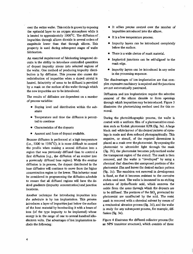
The manufacture of an integrated circuit begins with a large silicon wafer, usually 3 to 4 inches in diameter, as shown in fgure 2. The wafers themselves are cut in thin slices from a large uniform crystal grown under tightly controlled environmental and electrical con- ditions from a seed crystal (a small, single crystal of silicon having very few dislocations and oriented in the predetermined plane). The material is doped with the impurities (boron, antimony, and phosphorus) to produce the desired electrical characteristics. After being cut, the wafers are lapped on abrasive lapping machines to the thicknesses required for integrated circuits. The lapped wafers are polished and are then ready for the next phases of fabrication.
With this brief description of wafer processing, we can now proceed to a more detailed consideration of the individual wafer-processing steps. These steps will be considered in the order in which they are per- formed on integrated circuit wafers.
After the wafers are prepared, the next step in the fabrication process is epitaxial growth-the ordered growth of a monocrystalline layer on the single- crystal substrate so that the lattice structure of the resulting layer is an exact extension of the substrate crystal structure. It is in this epitaxial layer that the components of the integrated circuit are fabricated. A feature of epitaxy is that the doping of the epitaxial
2
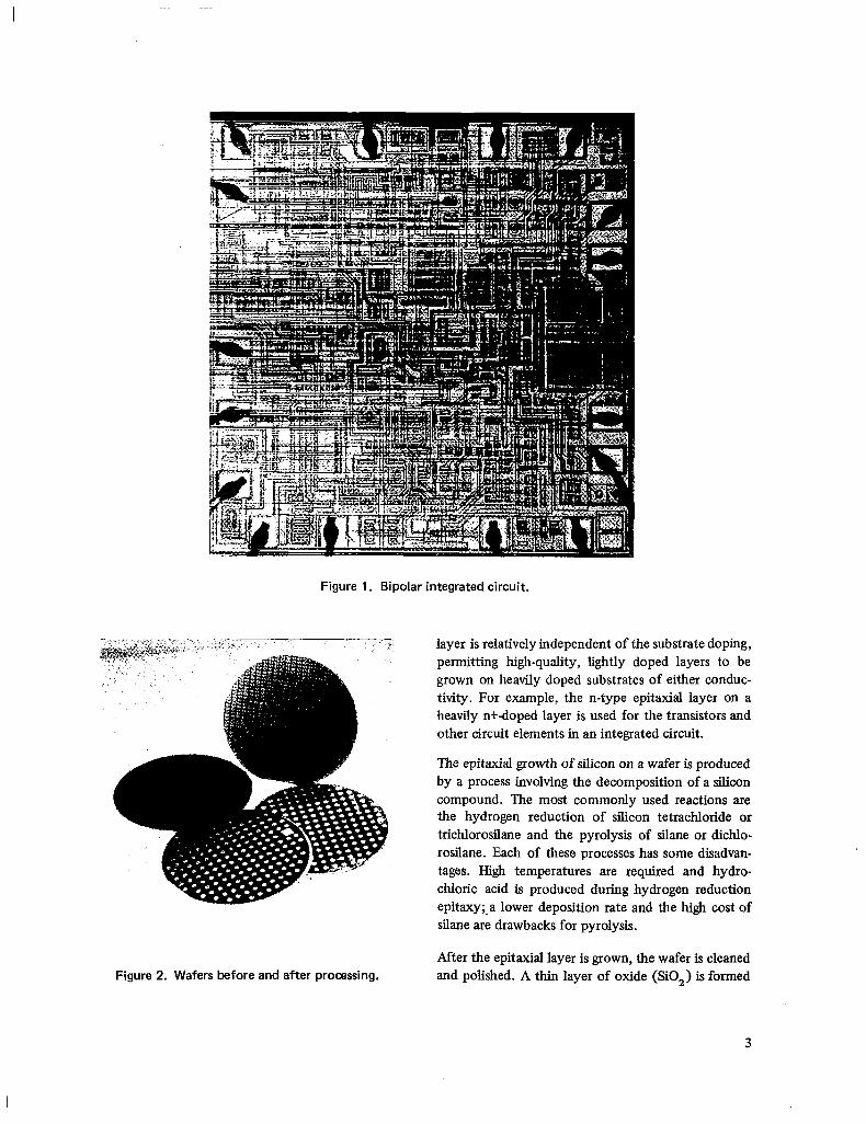
Figure 1. Bipolar integrated circuit.
Figure 2. Wafers before and after processing.
layer is relatively independent of the substrate doping, permitting high-quality, lightly doped layers to be grown on heavily doped substrates of either conduc- tivity. For example, the n-type epitaxial layer on a heavily n+-doped layer is used for the transistors and other circuit elements in an integrated circuit.
The epitaxial growth of silicon on a wafer is produced by a process involving the decomposition of a silicon compound. The most commonly used reactions are the hydrogen reduction of silicon tetrachloride or trichlorosilane and the pyrolysis of silane or dichlo- rosilane. Each of these processes has some disadvan- tages. High temperatures are required and hydro- chloric acid is produced during hydrogen reduction epitaxy;.a lower deposition rate and the high cost of silane are drawbacks for pyrolysis.
After the epitaxial layer is grown, the wafer is cleaned and polished. A thin layer of oxide (SiO,) is formed
3
over the entire wafer. This oxide is grown by exposing the epitaxial layer to an oxygen atmosphere while it is heated to approximately 1OOO’C. The diffusion of impurities through silicon dioxide is several orders of magnitude lower than that through silicon. This property is used during subsequent stages of wafer fabrication.
An essential requirement of fabricating integrated cir- cuits is the ability to introduce controlled quantities of dopant impurity atoms into selected regions of the wafer. One method of producing impurity distri- bution is by diffusion. This process also causes the redistribution of impurities when a doped crystal is heated. Selectivity of areas to be diffused is provided by a mask on the surface of the wafer through which the new impurities are to be introduced.
The results of diffusion are dependent on a number of process variables:
l Doping level and distribution within the sub- strate
l Temperature and time the diffusion is permit- ted to continue
l Characteristics of the dopants
l Amount and form of dopant available.
Because diffusion is performed at a high temperature (i.e., 1000 to 1350°C), it is more difficult to control the profile when making a second diffusion into a region that was previously diffused than to control a first diffusion (e.g., the diffusion of an emitter into a previously diffused base region). While the emitter diffusion is in process, the dopant distributed in the base diffusion will continue to move from the higher concentration region to the lower. This behavior must be considered in programming the diffusion schedule to ensure that all diffused regions will have the de- sired gradients (impurity concentration) and junction locations.
Another technique for introducing impurities into the substrate is by ion implantation. This process introduces a layer of impurities just below the surface of the host material by bombarding it with a beam of ions (of the type impurity to be implanted) whose energy is in the range of one to several hundred kilo- electron volts. The advantages of ion implantation in- clude the following:
It offers precise control over the number of impurities introduced into the silicon.
It is a low temperature process.
Impurity layers can be introduced completely below the surface.
There is a wide choice of mask material.
Implanted junctions can be self-aligned to the mask edge.
Impurity layers can be introduced in any order in the processing sequence.
The disadvantages of ion implantation are that com- plex expensive machinery is required and the junctions are not automatically passivated.
Diffusions and ion implantation require the selective removal of the silicon dioxide to form openings through which impurities may be introduced. Figure 3 illustrates the photoetching method used for this re- moval.
During the photolithographic process, the wafer is coated with a uniform film of a photosensitive emul- sion such as Kodak photoresist KPR (fig. 3a). A large black and white layout of the desired pattern of open- ings is made and then reduced photographically. This negative, or stencil, of the required dimensions is placed as a mask over the photoresist. By exposing the photoresist to ultraviolet light through the mask (fg. 3b), the photoresist becomes polymerized under the transparent region of the stencil. The mask is then removed, and the wafer is “developed” by using a chemical that dissolves the unexposed portions of the photoresist film and leaves the desired surface pattern (fig. 3~). The emulsion not removed in development is fured, so that it becomes resistant to the corrosive etches used next. The wafer is immersed in an etching solution of hydrofluoric acid, which removes the oxide from the areas through which the dopants are to be diffused. The portions of the SiO, protected by photoresist are unaffected by the acid. The resist mask is removed with a chemical solvent by means of a mechanical abrasion process (fig. 3d), and the wafer is ready for any subsequent process, for example, dif- fusion (fig. 3e).
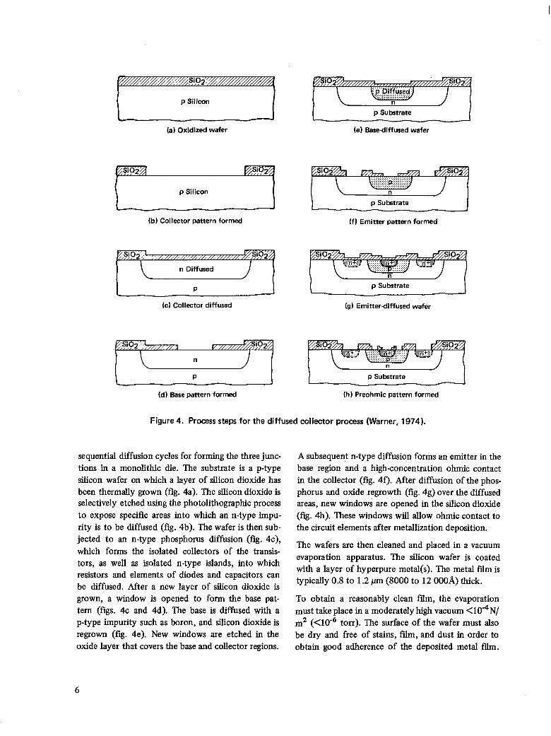
Figure 4 illustrates the diffused collector process (for an NPN transistor structure), which consists of three
4

Photosensitive
Si --) Si --)
(b)
(Cl (d)
. I 7.. ,. SiO 2-
Si - f!iiiiv :.;5:::.,0
~,..,-.:.;.,’ .;.-‘. -..p;-‘.~,‘*:
Figure 3. Photolithographic process steps.
5
lb) Collector pattern formed
(cl Collector diffused
Id) Base pattern formed
p Substrate I
(e) Base-diffused wafer
p substrate I
(f) Emitter pattern formed
(g) Emitterdiffused wafer
I p Substrate - -
(h) Preohmic pattern formed
Figure 4. Process steps for the diffused collector process (Warner, 1974).
sequential diffusion cycles for forming the three junc- tions in a monolithic die. The substrate is a p-type silicon wafer on which a layer of silicon dioxide has been thermally grown (fig. 4a). The silicon dioxide is selectively etched using the photolithographic process to expose specific areas into which an n-type impu- rity is to be diffused (fig. 4b). The wafer is then sub- jected to an n-type phosphorus diffusion (fig. 4c), which forms the isolated collectors of the transis- tors, as well as isolated n-type islands, into which resistors and elements of diodes and capacitors can be diffused. After a new layer of silicon dioxide is grown, a window is opened to form the base pat- tern (figs. 4c and 4d). The base is diffused with a p-type impurity such as boron, and silicon dioxide is regrown (fig. 4e). New windows are etched in the oxide layer that covers the base and collector regions.
A subsequent n-type diffusion forms an emitter in the base region and a high-concentration ohmic contact in the collector (fig. 4f). After diffusion of the phos- phorus and oxide regrowth (fig. 4g) over the diffused areas, new windows are opened in the silicon dioxide (fig. 4h). These windows will allow ohmic contact to the circuit elements after metallization deposition.
The wafers are then cleaned and placed in a vacuum evaporation apparatus. The silicon wafer is coated with a layer of hyperpure metal(s). The metal film is typically 0.8 to 1.2 lun (8000 to 12 OOOA) thick.
To obtain a reasonably clean film, the evaporation must take place in a moderately high vacuum <10S4N/ m2 (<10m6 torr). The surface of the wafer must also be dry and free of stains, film, and dust in order to obtain good adherence of the deposited metal fh.
6
Proper distance of the wafer from the evaporant source and location of the wafer with respect to the source are necessary to ensure uniform thickness of the evaporated layer(s) and to prevent thinning (shad- owing) of the layer over steps in the various oxide dif- fusion and contact windows. The thickness of the layer(s) is also controlled by the temperature of the source and the time allowed for deposition. After the metal layer(s) is deposited, the metallized surface within the area of the matrix of circuits on the silicon wafer must not be touched by tweezers or other handling tools.
The geometry of the metal contacts and interconnec- tion is produced by the inverse of the photolitho- graphic process used for creating windows in the oxide. The photoresist is placed on the metal layer on the silicon wafer, but is exposed to a pattern in which the interconnection design on the glass plate is trans- parent, rather than opaque. In developing the resist, all portions are washed away except the exposed pat- tern. The metal layer is etched, and all metal is attacked except the interconnection pattern, which is protected by the photoresist mask. The resist is stripped, and the wafer then has a matrix of circuits, complete with contacts and interconnections.
Thin-film components (discussed more fully in the following section), usually resistors, can be fabricated on top of the passivated silicon monolithic integrated circuit by using vacuum evaporation techniques similar to those used to deposit the interconnection metal- lization. The advantages of combining thin-film and semiconductor technologies are :
l Greater degree of design freedom
l Greater range of component values than those possible with diffused resistors
l Improved tolerances
l On-chip adjustment of resistance by laser trim- ming.
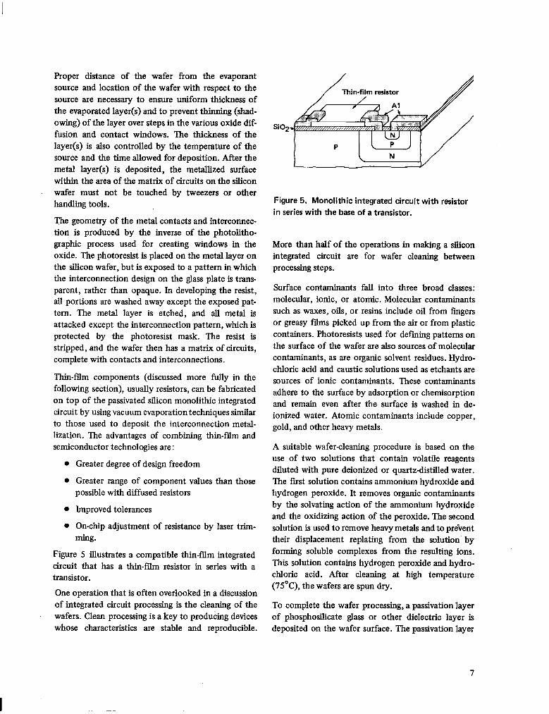
Figure 5 illustrates a compatible thin-film integrated circuit that has a thin-film resistor in series with a transistor.
One operation that is often overlooked in a discussion of integrated circuit processing is the cleaning of the wafers. Clean processing is a key to producing devices whose characteristics are stable and reproducible.
Figure 5. Monolithic integrated circuit with resistor in series with the base of a transistor.
More than half of the operations in making a silicon integrated circuit are for wafer cleaning between processing steps.
Surface contaminants fall into three broad classes: molecular, ionic, or atomic. Molecular contaminants such as waxes, oils, or resins include oil from fingers or greasy fdms picked up from the air or from plastic containers. Photoresists used for defining patterns on the surface of the wafer are also sources of molecular contaminants, as are organic solvent residues. Hydro- chloric acid and caustic solutions used as etchants are sources of ionic contaminants. These contaminants adhere to the surface by adsorption or chemisorption and remain even after the surface is washed in de- ionized water. Atomic contaminants include copper, gold, and other heavy metals.
A suitable wafer-cleaning procedure is based on the use of two solutions that contain volatile reagents diluted with pure deionized or quartz-distilled water. The fust solution contains ammonium hydroxide and hydrogen peroxide. It removes organic contaminants by the solvating action of the ammonium hydroxide and the oxidizing action of the peroxide. The second solution is used to remove heavy metals and to preGent their displacement replating from the solution. by forming soluble complexes from the resulting ions. This solution contains hydrogen peroxide and hydro- chloric acid. After cleaning at high temperature (79(Z), the wafers are spun dry.
To complete the wafer processing, a passivation layer of phosphosilicate glass or other dielectric layer is deposited on the wafer surface. The passivation layer
7
is a protective mechanism that can prevent conduc- tive residue particles that result from packaging from short-circuiting metallization. The passivation layer also contributes to a higher level of reliability by act- ing as getter (collector) or barrier to mobile ions left on the surface of the device after the final metalliza- tion wash. Other dielectric layers are plasma-deposited s&con nitride films or phosqhosilicate glass (I’SG), followed by a layer of polyimide plastic (Kapton). Windows in the passivation are cut out for external connection to the metallization.
Up to this point, all process steps were carried out on full silicon wafers. To utilize the wafers, they must be separated into individual chips; this step is accom- plished in the scribing and dicing operation. Before the actual scribing, the oxide on the wafer is prefer- entially removed along each scribing path so that scribing can be performed on bare silicon. This forms a scribe grid for the dicing operation.
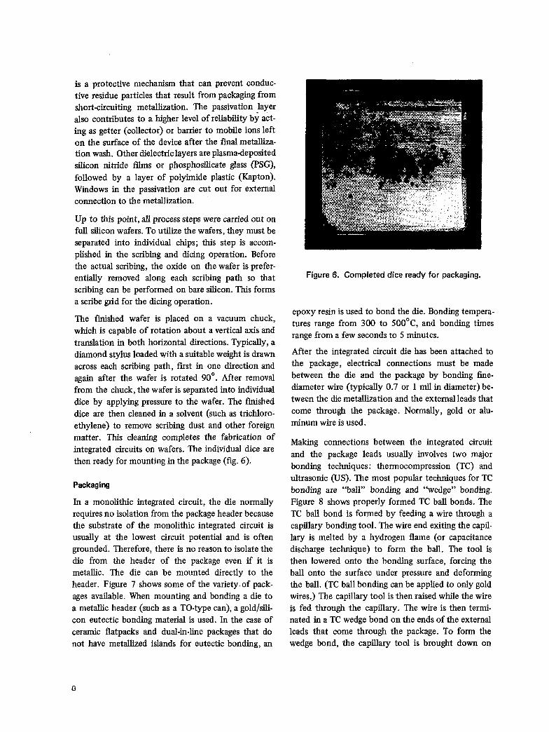
The finished wafer is placed on a vacuum chuck, which is capable of rotation about a vertical axis and translation in both horizontal directions. Typically, a diamond stylus loaded with a suitable weight is drawn across each scribing path, first in one direction and again after the wafer is rotated 90’. After removal from the chuck, the wafer is separated into individual dice by applying pressure to the wafer. The finished dice are then cleaned in a solvent (such as trichloro- ethylene) to remove scribing dust and other foreign matter. This cleaning completes the fabrication of integrated circuits on wafers. The individual dice are then ready for mounting in the package (fig. 6).
Packaging
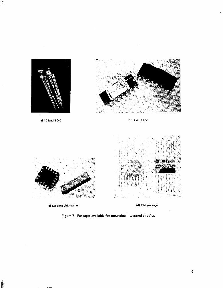
In a monolithic integrated circuit, the die normally requires no isolation from the package header because the substrate of the monolithic integrated circuit is usually at the lowest circuit potential and is often grounded. Therefore, there is no reason to isolate the die from the header of the package even if it is metallic. The die can be mounted directly to the header. Figure 7 shows some of the variety.of pack- ages available. When mounting and bonding a die to a metallic header (such as a TO-type can), a gold/sili- con eutectic bonding material is used. In the case of ceramic flatpacks and dual-m-line packages that do not have metallized islands for eutectic bonding, an
Figure 6. Completed dice ready for packaging.
epoxy resin is used to bond the die. Bonding tempera- tures range from 300 to SOO’C, and bonding times range from a few seconds to 5 minutes.
After the integrated circuit die has been attached to the package, electrical connections must be made between the die and the package by bonding fine- diameter wire (typically 0.7 or 1 rnil in diameter) be- tween the die metallization and the external leads that come through the package. Normally, gold or alu- minum wire is used.
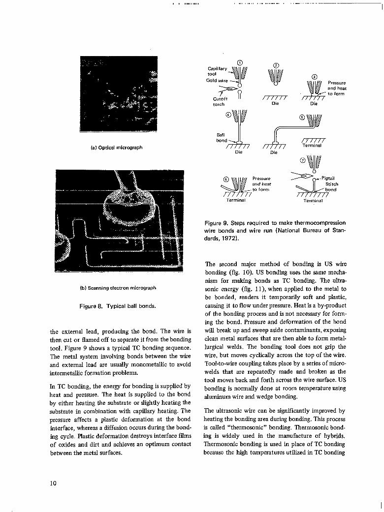
Making connections between the integrated circuit and the package leads usually involves two major bonding techniques: thermocompression (TC) and ultrasonic (US). The most popular techniques for TC bonding are “ball” bonding and “wedge” bonding. Figure 8 shows properly formed TC ball bonds. The TC ball bond is formed by feeding a wire through a capillary bonding tool. The wire end exiting the capil- lary is melted by a hydrogen flame (or capacitance discharge technique) to form the ball. The tool is then lowered onto the bonding surface, forcing the ball onto the surface under pressure and deforming the ball. (TC ball bonding can be applied to only gold wires.) The capillary tool is then raised while the wire is fed through the capillary. The wire is then termi- nated in a TC wedge bond on the ends of the external leads that come through the package. To form the wedge bond, the capillary tool is brought down on
lb) Dual-in-line (a) 1 O-lead TO-5
(c) Leadless chip carrier (d) Flat package
Figure 7. Packages available for mounting integrated circuits.
, .,, , ,. ,, , ,. .,,._. .., . .-_. ..-.__----- ________ -.-
(a) Optical micrograph Die Die
/7//// Terminal
lb) Scanning electron micrograph
Figure 8. Typical ball bonds.
the external lead, producing the bond. The wire is then cut or flamed off to separate it from the bonding tool. Figure 9 shows a typical TC bonding sequence. The metal system involving bonds between the wire and external lead are usually monometallic to avoid intermetahic formation problems.
In TC bonding, the energy for bonding is supplied by heat and pressure. The heat is supplied to the bond by either heating the substrate or slightly heating the substrate in combination with capillary heating. The pressure affects a plastic deformation at the bond interface, whereas a diffusion occurs during the bond- ing cycle. Plastic deformation destroys interface films of oxides and dirt and achieves an optimum contact between the metal surfaces.
Pressure and heat to form
Terminal Terminal
Figure 9. Steps required to make thermocompression wire bonds and wire run (National Bureau of Stan- dards, 1972).
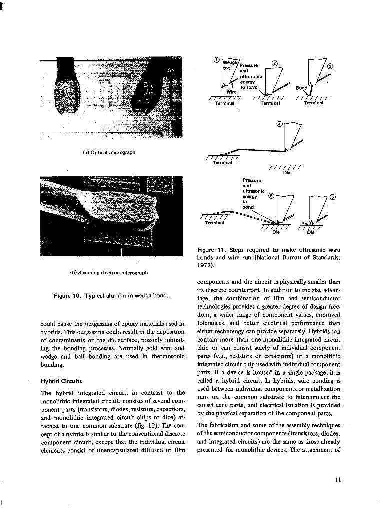
The second major method of bonding is US wire bonding (fig. 10). US bonding uses the same mecha- nism for making bonds as TC bonding. The ultra- sonic energy (fig. 11), when applied to the metal to be bonded, renders it temporarily soft and plastic, causing it to flow under pressure. Heat is a by-product of the bonding process and is not necessary for form- ing the bond. Pressure and deformation of the bond will break up and sweep aside contaminants, exposing clean metal surfaces ‘that are then able to form metal- lurgical welds. The bonding tool does not grip the wire, but moves cyclically across the top of the wire. Tool-to-wire coupling takes place by a series of micro- welds that are repeatedly made and broken as the tool moves back and forth across the wire surface. US bonding is normally done at room temperature using aluminum wire and wedge bonding.
The ultrasonic wire can be significantly improved by heating the bonding area during bonding. This process is called “thermosonic” bonding. Thermosonic bond- ing is widely used in the manufacture of hybrids. Thermosonic bonding is used in place of TC bonding because the high temperatures utilized in TC bonding
10
[email protected]$ ;z /////// Terminal Terminal Terminal
(a) Optical micrograph
(b) Scanning electron micrograph
Figure 10. Typical aluminum wedge bond.
could cause the outgassing of epoxy materials used in hybrids. This outgassing could result in the deposition of contaminants on the die surface, possibly inhibit- ing the bonding processes. Normally gold .wire and wedge and ball bonding are used in thermosonic bonding.
Hybrid Circuits
The hybrid integrated circuit, in contrast to the monolithic integrated circuit, consists of several com- ponent parts (transistors, diodes, resistors, capacitors, and monolithic integrated circuit chips or dice) at- tached to one common substrate (fig. 12). The con- cept of a hybrid is similar to the conventional discrete component circuit, except that the individual circuit elements consist of unencapsulated diffused or film
components and the circuit is physically smaller than its discrete counterpart. In addition to the size advan- tage, the combination of film and semiconductor technologies provides a greater degree of design free- dom, a wider range of component values, improved tolerances, and better electrical performance than either technology can provide separately. Hybrids can contain more than one monolithic integrated circuit chip or can consist solely of individual component parts (e.g., resistors or capacitors) or a monolithic integrated circuit chip used with individual component parts-if a device is housed in a single package, it is called a hybrid circuit. In hybrids, wire bonding is used between individual components or metallization runs on the common substrate to interconnect the constituent parts, and electrical isolation is provided by the physical separation of the component parts.
The fabrication and some of the assembly techniques of the semiconductor components (transistors, diodes, and integrated circuits) are the same as those already presented for monolithic devices. The attachment of
11

Figure 12. Hybrid integrated circuit.
12
the chips onto the ceramic substrate and the substrate onto the package header involves processes identical to monolithic integrated circuit bonding techniques. Some technologies and processes, such as thin and thick films, are unique to hybrids and will be dis- cussed here.
Film circuits usually contain only resistors, capacitors, and conductor patterns. Film circuits are often sup- plemented by silicon transistors, diodes, and/or inte- grated circuit chips to form hybrid circuits. Materials used for these films include aluminum, nichrome, titanium, tantalum, tantalum pentoxide, gold, palla- dium, platinum, manganese oxide, and copper.
Thin films are deposited on inert substrates by chemi- cal or vapor deposition techniques. These films are usually hundreds of angstroms to several microns thick. ‘Ihe substrate commonly used for thin-film circuits is of tine-grained 99+ percent alumina. Alumina is probably the most popular substrate material because of its high thermal conductivity, good resistance to chemical attack, and high compres- sive strength for lead bonding. Beryllia is sometimes used when increased thermal conductivity is desirable. The least expensive substrate is glass. Silicon can serve as a substrate, but it must be coated with a dielectric layer of silicon dioxide.
Most of the film circuits (figs. 13a and b) consist of elements patterned from several thin films of different materials. It is possible to form the components directly by selectively depositing the films through masks. However, the most popular technique for pro- ducing thin-film circuits is the subtractive process in which a multilayer film is deposited uniformly over the substrate, followed by selective removal of the material from the individual layers to form the de- sired components. The chemicals used to etch films are basically the same as those used to dissolve bulk silicon, but they are more dilute, resulting in a reduced etch rate minimizing attack on the photoresist and the underlying film.
Anodization, another process used to alter thin films, is defmed as the electrochemical oxidation of a metal anode in an electrolytic cell. Anodization is used to form an adherent oxide film on certain metals called valve metals. Among these metals are tantalum, titanium, tungsten, and aluminum. Although the anodic process has been used to trim resistors to value
by creating an oxide at the expense of the parent film, laser trimmin g has been displacing the anodic method. Laser machining can be used to alter the geometry (changing the electrical path) of a thin-film resistor to increase its total resistance. Whereas trim anodlza- tion causes the change in resistance by reducing the effective thickness of the fdrn and increasing its sheet resistance, laser trimming leaves the film properties substantially unchanged and varies the geometry.
Other types of thin films can be used for fabricating capacitors and conductor films, as well as resistors. The materials listed previously have specific prop- erties and methods of deposition that can provide optimum component characteristics.
Another type of circuit used in the fabrication of hybrids is the thick-film circuit (fig. 13~). A thick- film circuit consists of passive components that are formed in place on the substrates by the selective application of materials in the form of pastes. These pastes are subsequently fired at high temperatures to form the desired films. As with thin-film circuits, discrete components such as transistor and integrated circuit chips are added to form a thick-film hybrid integrated circuit. The vertical and horizontal dimen- sions of the film pattern are two to five times larger than those of thin films.
The chief passive components formed from thick films are conductive interconnections, high-precision resistor networks, and capacitors. The materials that will ultimately form the film are prepared as a suspen- sion of particles in a suitable organic vehicle of sol- vents. The suspended materials are then forced through a patterned screen to form the desired pat- tern. These thick-film inks, as they are called, consist of some or all of the following:
Finely divided metal or alloy powders that give the film cohesion or joinability. For conductive films, these metals determine electrical conduc- tivity.
Metallic oxides that, for resistive films, deter- mine the film resistivity.
Finely divided glass frits, which chiefly deter- mine the adherence of the film to the substrate and of different metals in the film to each other.
An organic vehicle for providing basic flow properties. Among these agents are solvents
13
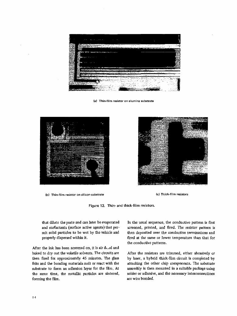
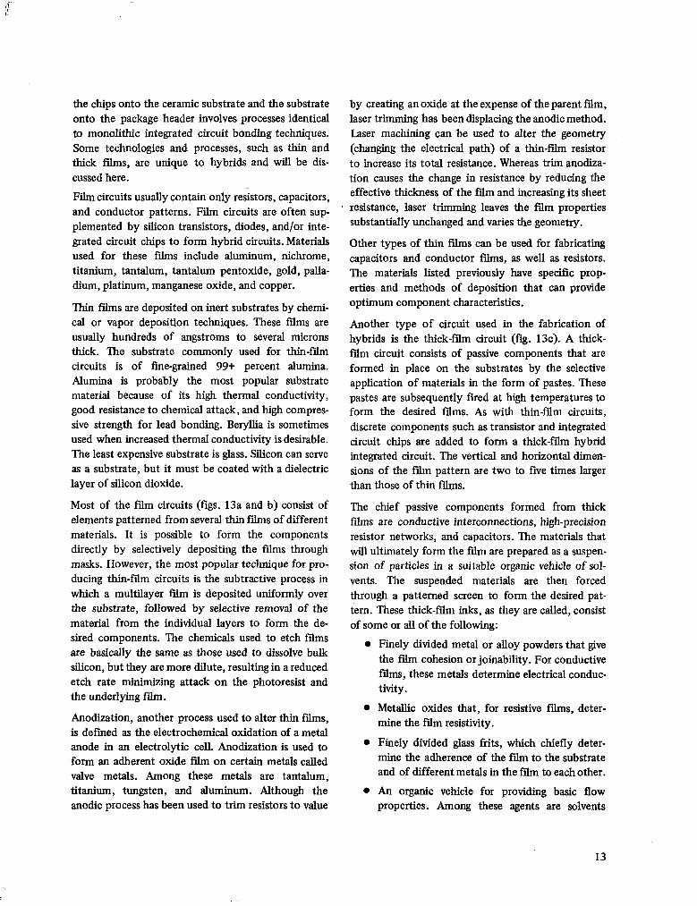
(a) Thin-film resistor on alumina substrate
(b) Thin-film resistor on silicon substrate (cl Thick-film resistors
Figure 13. Thin- and thick-film resistors.
that dilute- the paste and can later be evaporated and surfactants (surface active agents) that per- mit solid particles to be wet by the vehicle and properly dispersed within it.
After the ink has been screened on, it is air dl.cd and baked to dry out the volatile solvents. The circuits are then fired for approximately 45 minutes. The glass frits and the bonding materials melt or react with the substrate to form an adhesion layer for the film. At the same time, the metallic particles are sintered, forming the film.
In the usual sequence, the conductive pattern is first screened, printed, and fired. The resistor pattern is then deposited over the conductive terminations and fired at the same or lower temperature than that for the conductive patterns.
After the resistors are trimmed, either abrasively or by laser, a hybrid thick-film circuit is completed by attaching the other chip components. The substrate assembly is then mounted in a suitable package using solder or adhesive, and the necessary interconnections are wire bonded.
14
MONOLITHIC CIRCUIT DEFECTS
Die
Metalliza tion
Metallization defects result from either mishandling or flaws in the photolithographic process. To observe defects in the metallization, a magnification of 100X to 200X is normally used (per MIL-STD883B, Method 2010). However, with the new VLSI devices, higher magnifications will be needed to adequately examine the metallization.
Figure 14a is a photomicrograph of a VLSI memory device with a defect that is difficult to distinguish under the precap examination criteria of 100X to 200X. If the magnification is tripled, the defect shows up as a disturbed area (scratch) of metallization (fig. 14b). The scratch resulted in an open-circuited metal- lization stripe that caused the device to malfunction. Because examining complex devices at higher magni- fications requires an amount of time that is not nor- mally available to a precap inspector, the following paragraphs will address those metallization defects that are easily observable at 100X to 200X.
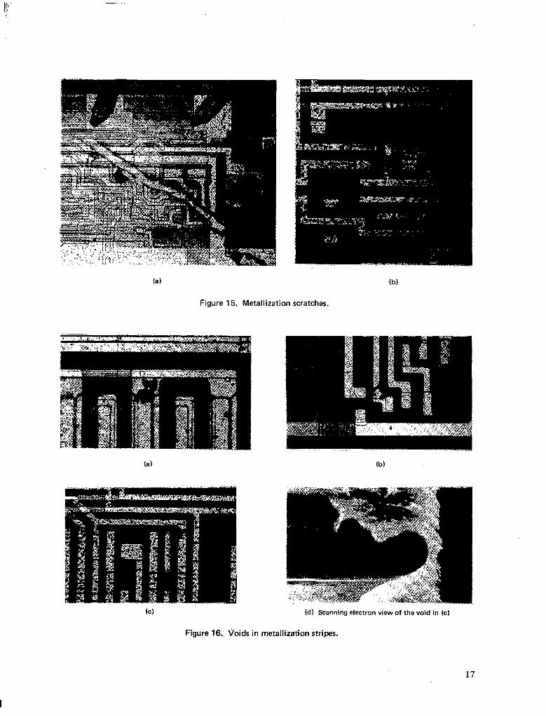
TWO of the most common kinds of metallization de- fects are scratches and voids. A scratch (fig. 14b) can be defined as any tearing defect, including probe marks, in the surface of the metallization. Scratches most often result from mechanical or mishandling damage; wafer probing is one source of scratches in metallization (fig. 15). Each circuit on a silicon wafer is electrically tested (either on a 100 percent basis or by sampling) after contact is established by means of fine-pointed micropositioned probes. (This test is performed to screen out bad devices before pack- aging.) The actual motion of the probes is mechani- cally controlled by an operator or automatic test equipment. This motion often results in a scrubbing motion that causes scratches in the metallization. Because it is softer than other metal systems (i.e., titanium/tungsten and gold/molybdenum), aluminum is particularly susceptible to scratching, smearing, and other deformations.
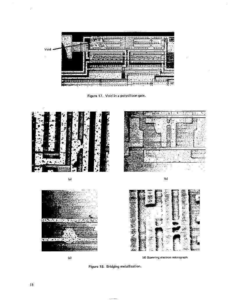
Voids are the result of an inadvertent etching of the metallization in the photolithographic process. A void can be defined as any region in the metallization where underlying metal or passivation is visible that is not caused by a scratch (fig. 16). The inadvertent etching
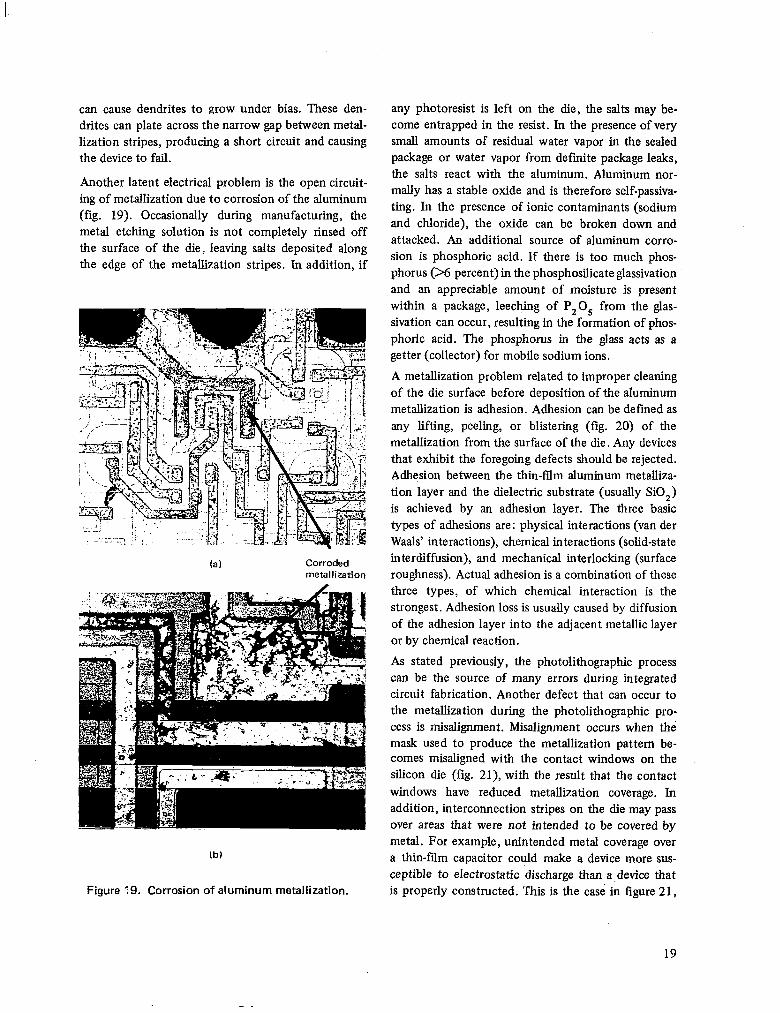
could cause an interconnection stripe to be severely reduced in width (as will also happen with scratches). Therefore, current in the metallization stripe is crowded through a very narrow region. As a conse- quence of this, electromigration of the aluminum atoms can occur, possibly resulting in the open-cir- cuiting of the stripe. With the new VLSI devices, two- and three-layer interconnection systems, such as polysilicon/aluminum or aluminum/aluminum, are being used, making it more difficult for inspectors to detect voids in underlying interconnect layers (fig. 17). MIL-STD-883B lists the following rejection cri- teria for scratches and voids:
A scratch or a void in the metallization stripe that reduces the width of the metalhzation stripe to less than one-half of the minimum de- signed width (fig. 16~).
A scratch in the metallization over a passivation step that leaves less than 7.5 percent of the original metal width at the step undisturbed (fig. 16a).
Void(s) in the metallization over the gate oxide bridge that leaves less than 75 percent of the metallization length and width between the source and drain diffusions undisturbed (fig. 17).
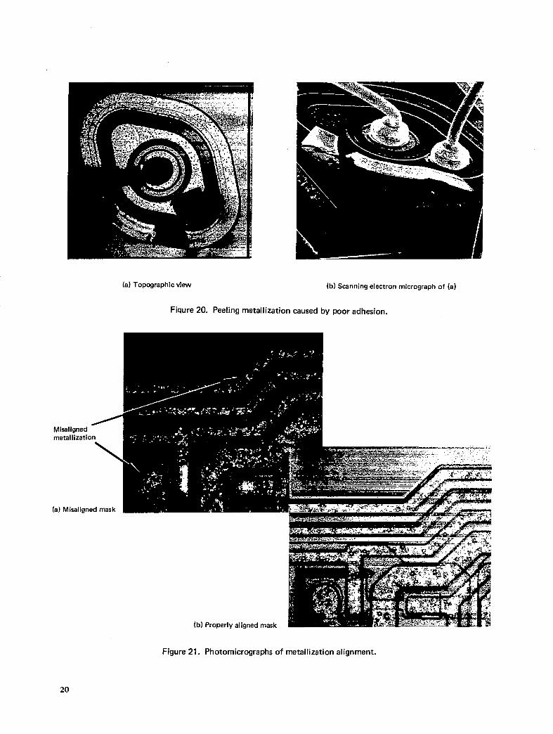
Bridging metallization is the result of incomplete etch- ing during the photolithographic process. Two con- ditions can occur from this type of defect:
l An unetched metallization path is left between adjacent metallization stripes (figs. 18a, b, and d), between adjacent contact windows, or be- tween an adjacent contact window and metalli- zation stripe(s).
l An unetched metallization path is left between adjacent stripes; however, the path begins at one stripe and terminates very close to the other stripe, but does not touch it (fig. 18~).
The fast defect produces a direct short circuit and is detectable during a precap examination or electrical tests. The second phenomenon often escapes visual detection and is usually not detectable electrically. If the die is not glassivated or if the glassivation is of high porosity, high moisture content in the package
15
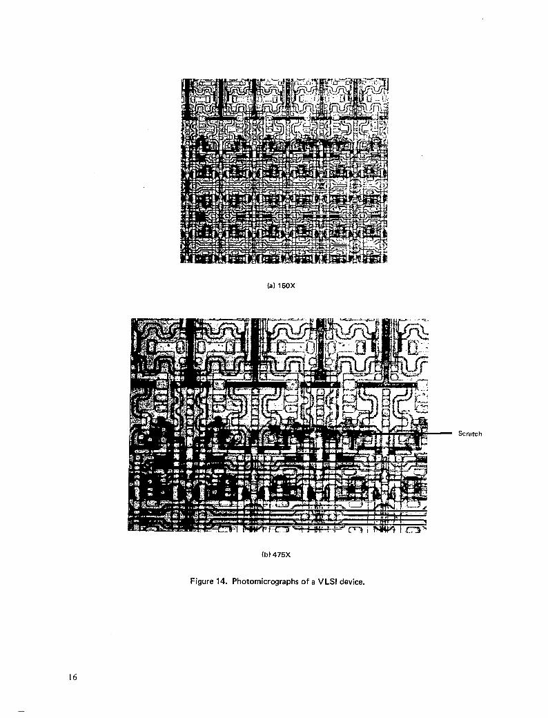
(a) 150X
(b) 475X
Figure 14. Photomicrographs of a VLSI device.
16
(a) (b)
Figure 15. Metallization scratches.
(a) (b)
(d) Scanning electron view of the void in (c)
Figure 16.. voids in metallization stripes.
Void
-
Figure 17. Void in a polysilicon gate.
(c)
Figure 18. Bridging metallization.
18
(d) Scanning electron micrograph
can cause dendrites to grow under bias. These den- drites can plate across the narrow gap between metal- lization stripes, producing a short circuit and causing the device to fail.
Another latent electrical problem is the open circuit- ing of metallization due to corrosion of the aluminum (fig. 19). Occasionally during manufacturing, the metal etching solution is not completely rinsed off the surface of the die, leaving salts deposited along the edge of the metallization stripes. In addition, if
(a) Corroded metallization
IbJ
Figure 19. Corrosion of aluminum metallization.
any photoresist is left on the die, the salts may be- come entrapped in the resist. In the presence of very small amounts of residual water vapor in the sealed package or water vapor from defmite package leaks, the salts react with the aluminum. Aluminum nor- mally has a stable oxide and is therefore self-passiva- ting. In the presence of ionic contaminants (sodium and chloride), the oxide can be broken down and attacked. An additional source of aluminum corro- sion is phosphoric acid. If there is too much phos- phorus (X percent) in the phosphosilicate glassivation and an appreciable amount of moisture is present within a package, leeching of P,O, from the glas- sivation can occur, resulting in the formation of phos- phoric acid. The phosphorus in the glass acts as a getter (collector) for mobile sodium ions.
A metallization problem related to improper cleaning of the die surface before deposition of the aluminum metallization is adhesion. Adhesion can be defined as any lifting, peeling, or blistering (fig. 20) of the metallization from the surface of the die. Any devices that exhibit the foregoing defects should be rejected. Adhesion between the thin-film aluminum metalliza- tion layer and the dielectric substrate (usually SiO,) is achieved by an adhesion layer. The three basic types of adhesions are: physical interactions (van der Waals’ interactions), chemical interactions (solid-state interdiffusion), and mechanical interlocking (surface roughness). Actual adhesion is a combination of these three types, of which chemical interaction is the strongest. Adhesion loss is usually caused by diffusion of the adhesion layer into the adjacent metallic layer or by chemical reaction.
As stated previously, the photolithographic process can be the source of many errors during integrated circuit fabrication. Another defect that can occur to the metallization during the photolithographic pro- cess is misalignment. Misalignment occurs when the mask used to produce the metallization pattern be- comes misaligned with the contact windows on the silicon die (fig. 21), with the result that the contact windows have reduced metallization coverage. In addition, interconnection stripes on the die may pass over areas that were not intended to be covered by metal. For example, unintended metal coverage over a thin-film capacitor could make a device more sus- ceptible to electrostatic discharge than a-device that is properly constructed. This is the case in figure 21,
19
(a) Misaligned mask
(a) Topographic view (b) Scanning electron micrograph of (a)
Fiwre 20. Peeling metallization caused by poor adhesion.
Misaligned metallizatic
Figure 21. Photomicrographs of metallization alignment.
20

where a misaligned mask resulted in a system failure. Contact windows that are not completely covered by metallization can result in latent device failure. The small part of the contact window covered by metal- lization could develop a hot spot when a high current density is flowing through the contact. Electromigra- tion could open-circuit the metal after a period of time.
Listed below are some of the rejection criteria for in- specting contact windows. It wil. become more dif- ficult to enforce these criteria as device densities in- crease.
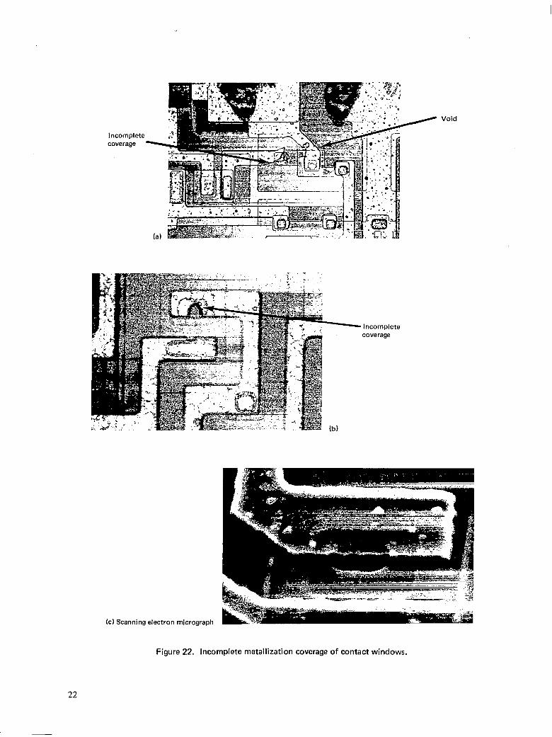
l Less than 75 percent of the area of the contact window is covered by metallization (fig. 22).
0 Less than a continuous 50 percent of the perimeter of the contact window is covered by metallization.
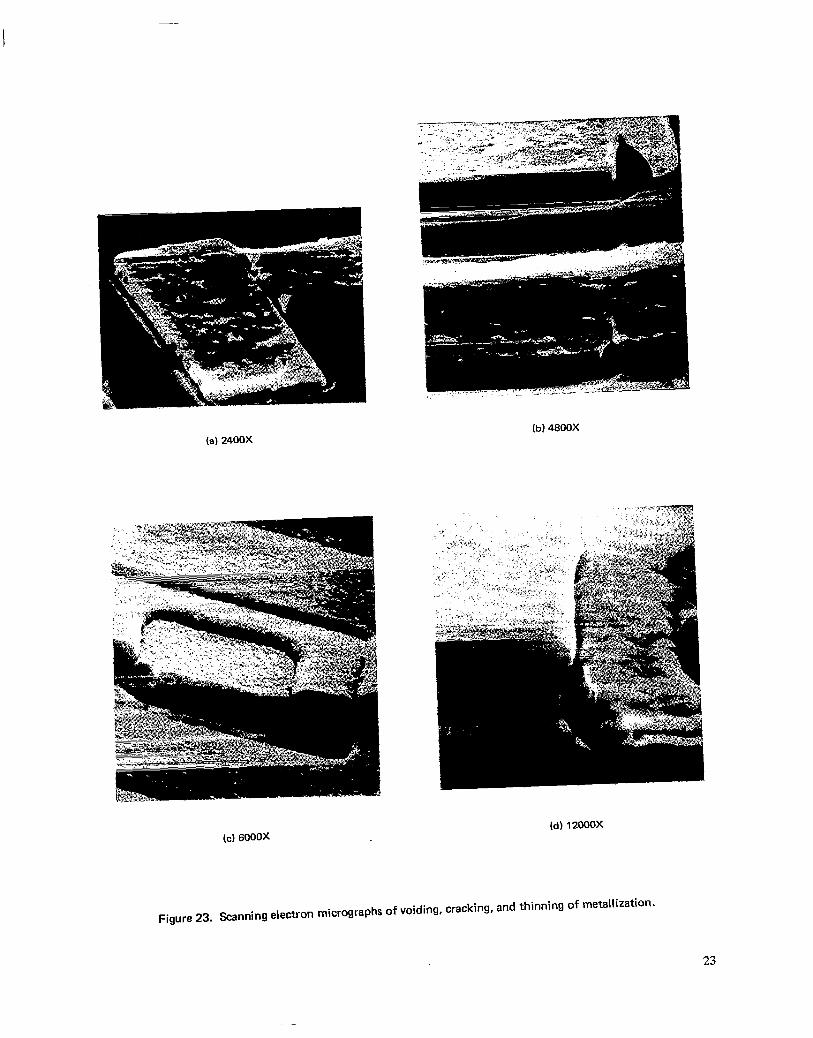
Some metallization defects are not readily observable during a precap examination. Normally, a scanning electron microscope is needed to view these defects. However, because it is important for the precap in- spector to understand these defects, they are presented here. The problem arises with the coverage of metal- lization over the edges of oxide (oxide steps). Gen- erally, during manufacturing, the oxide step is prefer- entially etched to provide a beveled edge. If the oxide step is not etched properly, it can have a very steep angle. A steep oxide step causes voiding, cracking, and thinning of the metallization (fig. 23). Latent open-circuit failures can occur from electromigration of the metal at these areas. Cracks and voids can also occur at contact window cutouts (fig. 23~).
Diffusion, Passivation, and Dielectric Isolation
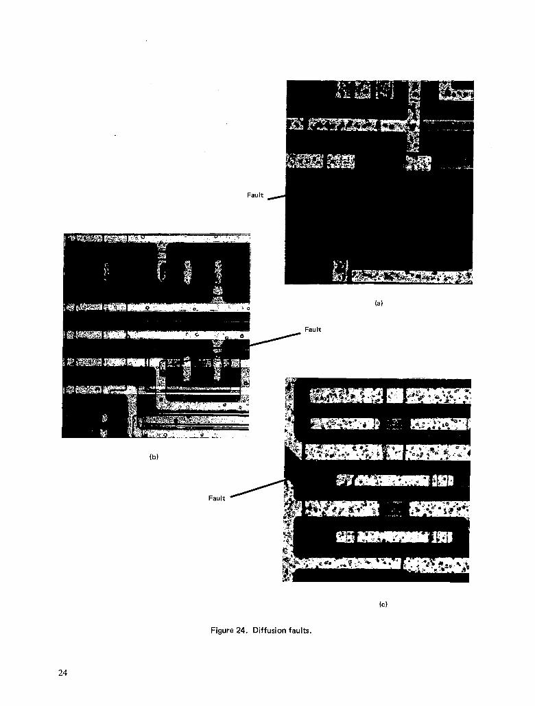
Diffusion, passivation, and dielectric isolation faults are normally the result of defects or inconsistencies in the photolithographic process. Two diffusion-type faults are of most concern in precap visual examina- tions. Any diffusion fault that allows bridging be- tween diffused areas is unacceptable (fig. 24a). Faults like this can be traced to lifting and peeling of the photoresist, causing exposure irregularities. These faults could manifest themselves as resistive short cir- cuits between two diffused areas. Figures 24a and 24b show some diffusion irregularities.
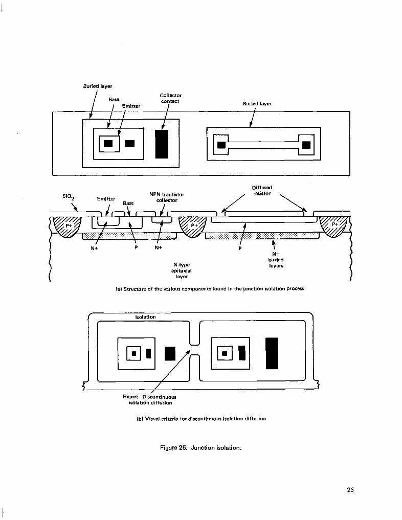
The second type of diffusion fault deals with junction isolation. In integrated circuit design, junction isola- tion (fig. 25a) can be used to prevent undesired elec- trical interconnection between regions in the same silicon substrate. These isolation areas are formed by the diffusion process. Processing faults can cause a discontinuity in the isolation diffusion. If this occurs, adjacent isolated areas are short-circuited (fig. 25b). This is an unacceptable defect. Even if the isolation diffusion is continuous, it can be reduced in width. If sufficiently reduced in width, the depletion layers of the isolated regions could spread far enough to touch each other. Similar defects (reduction in width) can also occur in diffused resistors. T’his changes the resistance of the resistor and might affect the circuit operation only under unusual circumstances that are not normally covered during electrical testing. Some of the rejection criteria for diffusion faults are:
0 Any isolation diffusion that is discontinuous.
l Any diffused area with less than 25 percent of the original diffusion width.
l Any diffused resistor with less than 50 percent of the original diffusion width.
Passivation faults are defects in the silicon dioxide that are detectable by a thinning or absence of passi- vation (silicon dioxide). Masking problems are the major contributor to passivation faults. Passivation faults become rejectable when they exist underneath metallization stripes (fig. 26). If the passivation fault is deep enough, the metallization could short circuit underlying conductors or even the silicon substrate. The depth of the passivation fault can be estimated by the number of lines observable at the edge of the fault. Even though the depth of the fault does not cause short circuits, the oxide may be thin enough to break down during electrical operation over the life of the device.
Active junction areas not covered by passivation, un- less by design, are r-ejectable. If not covered by passi- vation, junction areas are susceptible to mobile charges on the surface that can cause junction leakage cur- rents and lower breakdown voltages.
Occasionally, cutouts in the passivation for contact windows extend across a junction area because of a
21
Incomplete
Void
(c) Scanning electron micrograph
Figure 22. lnco lmplete metallization coverage of contact windows.
- Incomplete coverage
b)
22
-
(b) 4800X (a) 2400X
(c) 6000X (d) 12000X
Figure 23. !Scanning electron micrographs of voiding, cracking, and thinning of metallization.
23
Fault I
(a)
Fau It
(b)
Figure 24. Diffusic m faults.
Buried layer
I Base
I Emitter
Collector contact
I Buried layer
Diffused
SiO NPN transistor resistor 2 Emitter collector / \
) /, \
I v///////f I I r-v
f... . . . . . :. .:.:.:.:.:.:.:.:.:.:.. :,:,:.:.:.:.: ~,~,~,~,~.~.~_~.~. . . . . . . . . . . . . . . . . . . . . . . . . . . . :.:.:.:.:.:: ,.:.:.:.:.:.:.:.:.:.:.:.:.:., ,.,_,_,._.,.,.,_,._. .:. ~,~,~,‘.‘.~.~.~.~.~ ::. ~.~.~,~.~.~.~.~.....~.~,~ ;,...;, . .;,.;; ,.,.;,. ,.,.;,.;, .;; ,.,.,.,.,.,.,.,.,.,., ,.,. / \ I I L
N-o/P epitaxial
layer
N+ buried layers
(al Structure of the various components found in the junction isolation process
Isolation
77
Reject-Gontinuous isolation diffusion
lb) Visual criteria for discontinuous isolation diffusion
Figure 25. Junction isolation.
25
Unacceptable passivation fault
(a)
(b)
Unacceptable passivation fault
Figure 26. Faults in silicon dioxide passiwation (a and b).
26
(d) Scanning electron micrograph of (c)
Figure 26. Faults in silicon dioxide passivation (c and d).
Unacceptable passivation fault
27
masking fault, unless called for in the design. When the metallization is deposited, a shorted junction re- sults. A good example would be the. cutout for a base contact window that unintentionally extends across to the collector. When the metal is deposited, a shorted collector-base junction results, producing a diode be- tween the shorted collector-base junction and the emitter.
Some manufacturers use a process called dielectric isolation to isolate individual active circuit elements. Each circuit element is surrounded on the sides and bottom by an insulating layer of silicon dioxide (fig. 27). If problems occurred during processing due to masking faults, isolation regions could be bridged, resulting in a short circuit between active regions. This type of fault is detectable by the absence of a continuous isolation line (fig. 28a) between adjacent active areas. (Each active area is in reality a diffusion tub.) The isolation line is typically a black line whose discontinuity is easily recognized. A similar rejectable defect is a discontinuous isolation around each active area. Diffusions that are made into an active tub area are sometimes offset because of small alignment prob- lems. Defects such as this are rejectable if an over- lapping diffused area comes closer than 0.1 mil to an adjacent tub or an overlap of more than one diffusion into the dielectric isolation material occurs (fig. 28b).
Rejectable defects that can occur in the glassivation are numerous. Crazing of the glassivation is one de- fect that is rejectable because it usually prohibits detection of any defects under the glassivation. When crazing occurs, the glassivation has small, numerous, interconnected cracks that obscure the underlying silicon. Crazing occurs in the dicing operation when the wafer is turned upside down and broken into individual dice. If the surface is not cleaned between operations, small particles of silicon impact on the glassivation surface when pressure is applied to the wafer to break it up.
Glassiva tion
At times during the manufacturing process, a defect occurs in the mask used to generate the glassivation pattern, or the photoresist does not adhere properly. When this occurs, areas of metallization on the die are left uncovered by glassivation. If two or more active adjacent metallization stripes are left uncovered, the device is rejectable (fig. 29). Uncovered active areas of metallization can be resistively short-circuited if conductive particles come to rest in the area.
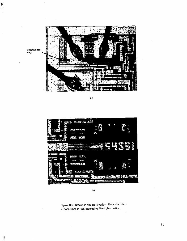
Cracks (not crazing) often occur in vapor-deposited glassivations. Vapor glassivations are in tensile stress. If the adhesion of the glassivation to the die surface is poor, localized lifting or cracking of the glassivation
PNP transistor
NPN transistor
\ Polycrystalline substrate
Figure 27. Dielectric isolation.
28
Reject
(a) Visual criteria for isolation lines
Overlap area
lb) Two diffusions overlapping into the dielectric material
Figure 28. Dielectric isolation visual criteria.
29
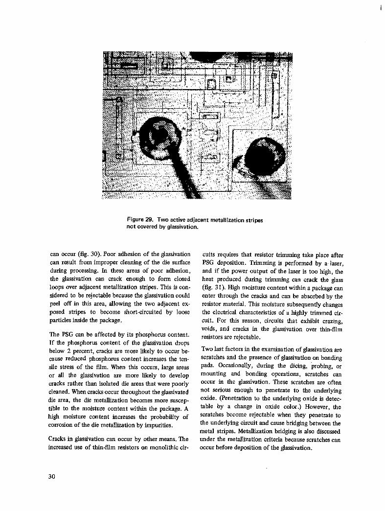
Figure 29. Two active adjacent metallization stripes not covered by glassivation.
can occur (fig. 30). Poor adhesion of the glassivation can result from improper cleaning of the die surface during processing. In these areas of poor adhesion, the glassivation can crack enough to form closed loops over adjacent metahization stripes. This is con- sidered to be rejectable because the glassivation could peel off in this area, allowing the two adjacent ex- posed stripes to become short-circuited by loose particles inside the package.
The PSG can be affected by its phosphorus content. If the phosphorus content of the glassivation drops below 2 percent, cracks are more likely to occur be- cause reduced phosphorus content increases the ten- sile stress of the film. When this occurs, large areas or all the glassivation are more likely to develop cracks rather than isolated die areas that were poorly cleaned. When cracks occur throughout the glassivated die area, the die metalhzation becomes more suscep- tible to the moisture content within the package. A high moisture content increases the probability of corrosion of the die metallization by impurities.
Cracks in glassivation can occur by other means. The increased use of thin-film resistors on monolithic cir-
cuits requires that resistor trimming take place after PSG deposition. Trimming is performed by a. laser, and if the power output of the laser is too high, the heat produced during trimming can crack the glass (fig. 3 1). High moisture content within a package can enter through the cracks and can be absorbed by the resistor material. This moisture subsequently changes the electrical characteristics of a highly trimmed cir- cuit. For this reason, circuits that exhibit crazing, voids, and cracks in the glassivation over thin-film resistors are rejectable.
Two last factors in the examination of glassivation are scratches and the presence of glassivation on bonding pads. Occasionally, during the dicing, ‘probing, or mounting and bonding operations, scratches can occur in the glassivation. These scratches are often not serious enough to penetrate to the underlying oxide. (Penetration to the underlying oxide is detec- table by a change in oxide color.) However, the scratches become rejectable when they penetrate to the underlying circuit and cause bridging between the metal stripes. Metallization bridging is also discussed under the metallization criteria because scratches can occur before deposition of the glassivation.
30
tnterference rings
(a)
(b)
Figure 30. Cracks in the glassivation. Note the inter- ference rings in (a), indicating lifted glassivation.
31
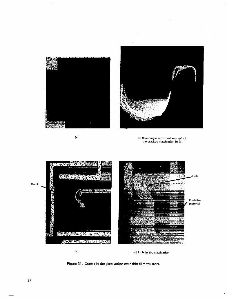
(a) (b) Scanning electron micrcgraph of the cracked glassivation in (a)
-Hole
Crack
(cl (d) Hole in the glassivation
Figure 31. Cracks in the glassivation over thin-film resistors.
32
Resistive material
The presence of glassivation on a bonding pad is caused by a defect in the photolithographic process. In general, glassivation that covers more than 25 percent of a bonding pad area is considered to be rejectable. The presence of glassivation on bonding pads is easier to detect at the wafer level before the bonding pro- cess. After bonding, the bonds obscure the presence of the glassivation on the pad. Bonds that. are made on glassivated pads are usually weak, although they are physically acceptable in appearance. The pres- ence of the glassivation inhibits the interfacial welding during the bonding process because it is difficult to break the glassivation to obtain metal-to-metal con- tact. Weak bonds as described above can be screened out by nondestructive bond pull tests.
Scribing
During the scribing process, small cracks can be intro- duced along the edges of a chip. The cracks develop when the diamond point tears the silicon during scribing. This is not as big a problem with dice that have been laser scribed. Cracks can also develop when the wafer is broken into individual chips. When cracks occur, some of them inevitably point toward the active portions of the chip. If a crack later propagates into the active circuit areas, it could degrade junctions by creating leakage paths and/or partially or com- pletely open circuit the metallization stripes. Some cracks have been observed to propagate under alumi- num metallization without open circuiting the stripe. In one case, the aluminum actually stretched over the crack, allowing the circuit to operate under worst- case conditions. Because it is difficult to provide effective screens for cracks, it is imperative that they be detected during the precap visual examination.
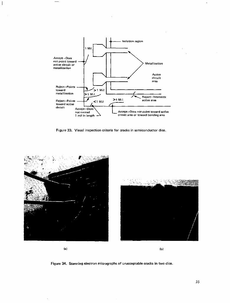
MIL-STD883B, Method 2010, lists the folIowing rejection criteria for cracks:
0 A crack in the active circuit area
l A crack that exceeds 3.0 mils in length or comes closer than 0.25 mil to any operating metallization or circuit element
l A crack that exceeds 1.0 mil in length inside the scribe line that points toward functional cir- cuit elements or metallization.
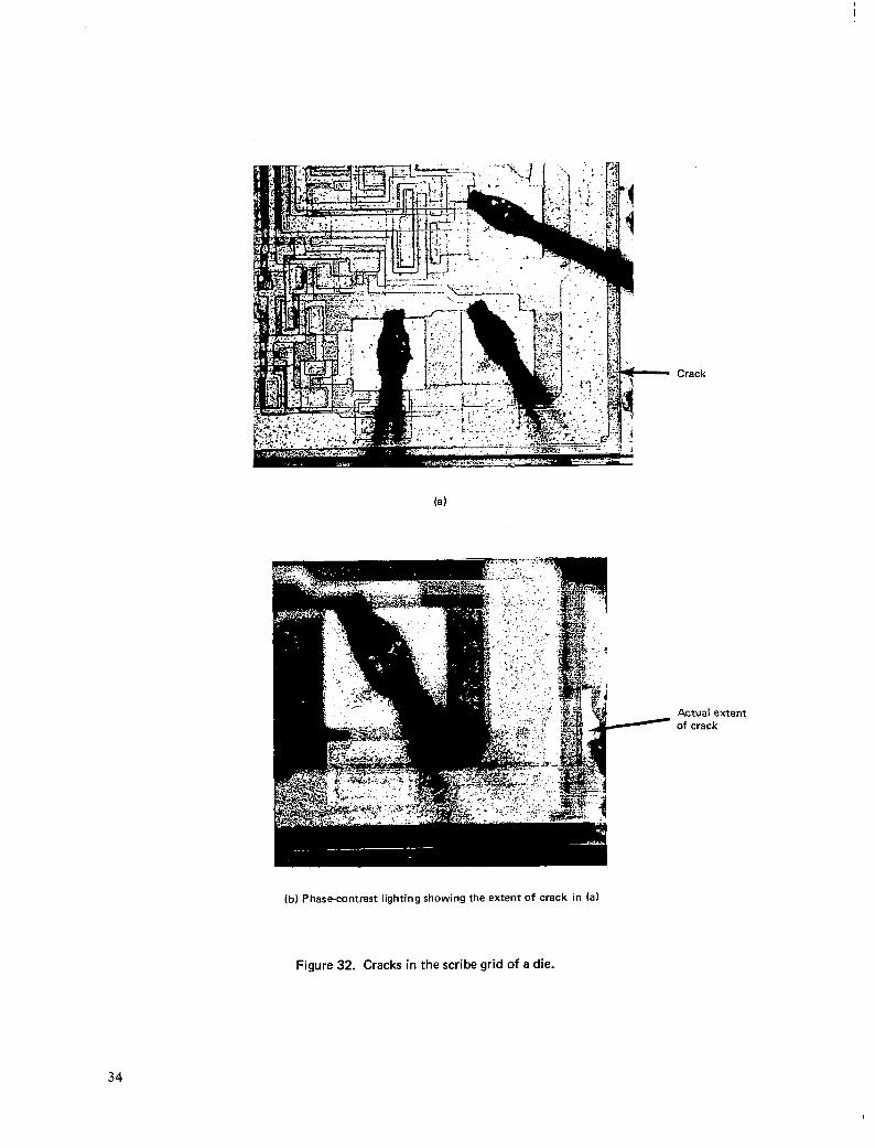
Unless proper lighting is used during precap screening, devices with cracks can sometimes look acceptable.
Figure 32a shows cracks in the scribe area under nor- mal bright-field lighting. Note that some of the cracks come too close to active operating metahization to be acceptable. If phasecontrast lighting is used, the actual extent of the crack can be seen (fig. 32b). A defect of this type is rejectable. In the course of nor- mal precap examinations, however, the time required for individual microcircuit attention such as that de- scribed above usually cannot be spared. Figure 33 illustrates the rejection criteria for cracks, and figure 34 shows cracks in dice.
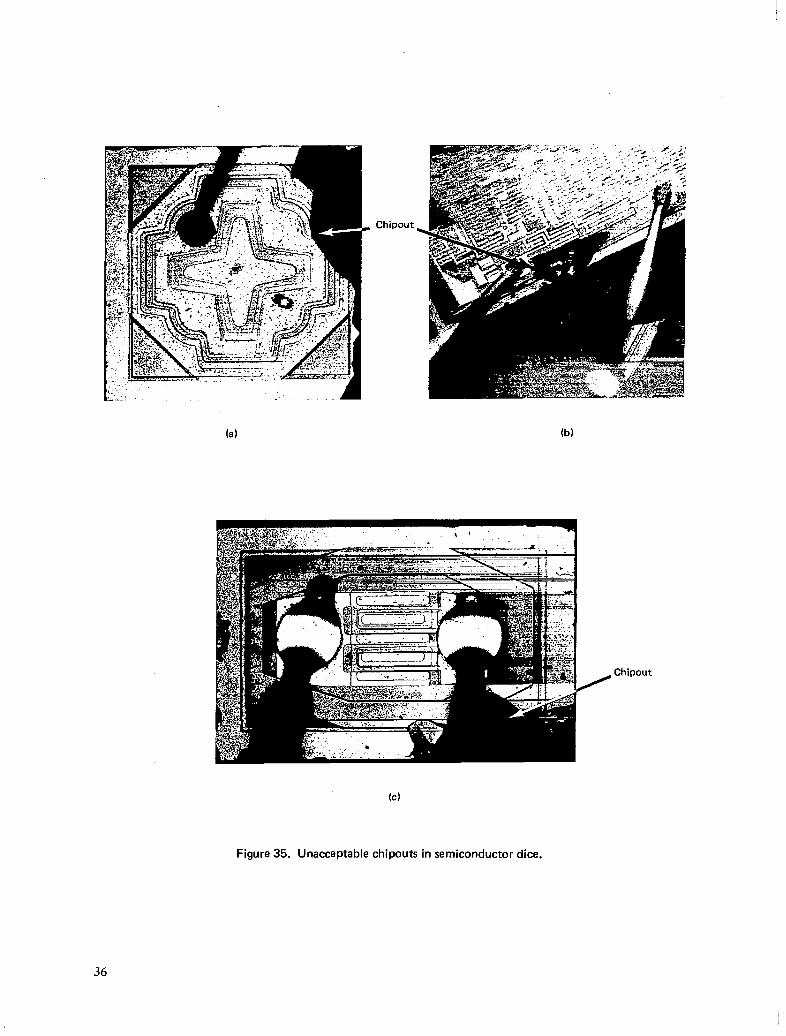
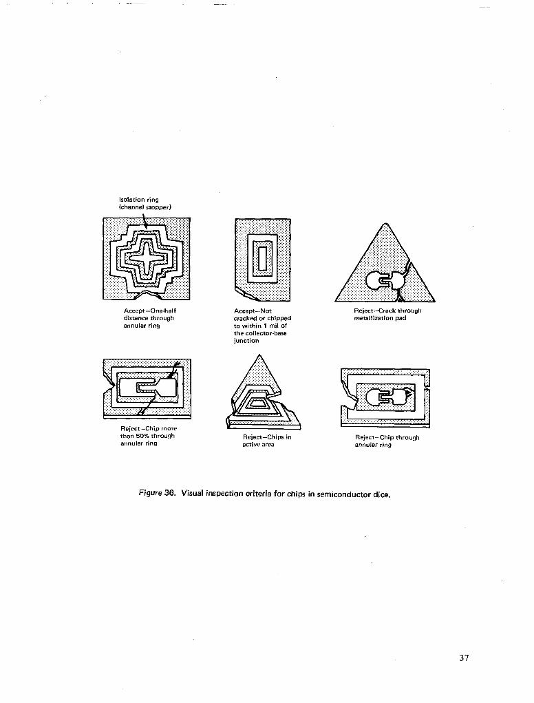
Other defects that can occur in the scribing operation are chipouts in the die. Chipouts occur when the wafer has not been completely scribed. In the sub- sequent breakup of the wafer, the silicon fractures rather than breaking cleanly along the scribe line. Chipouts can also occur during subsequent handling operations (fig. 35b), such as when the die is being mounted inside the package. The photographs in fig- ure 35 show some rejectable chipouts in dice. Figure 36 illustrates the rejection criteria for chipouts.
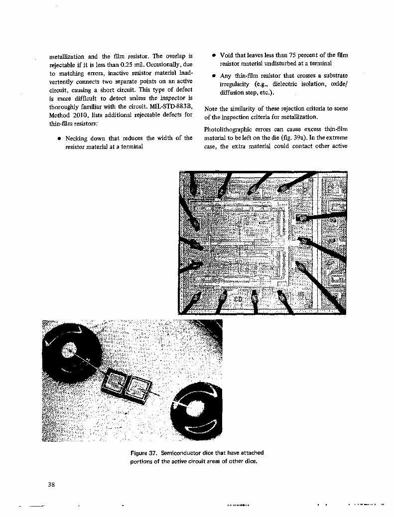
If the wafer is not aligned properly during the scrib- ing operation, scribing takes place along some plane other than the scribe grid. When this occurs, some dice will have attached portions of active circuit area of other dice-a rejectable defect (fig. 37).
Thin-Film Resistors
A thin-film resistor consists of a thin resistive film that is deposited on an insulating substrate. The film materials used are metals, metal alloys, and metal compounds such as gold, palladium, palladium/gold, and titanium. More and more, manufacturers are using thin-fnm resistors in analog circuitry, particu- larly in digital-to-analog and analog-to-digital conver- ters.
Because thin-film resistors are deposited by a separate process similar to aluminum metallization, misalign- ments can occur. Any misaligmnent between the con- ductor/resistor in which the actual width of the over- lap is less than 50 percent of the original resistor width is unacceptable (fig. 38). This criterion is analo- gous to the 50 percent reduction rejection criterion of metallization conductors discussed previously. Mis- alignment of more than 50 percent could cause prob- lems due to electromigration. Similar problems can occur if there is not enough overlap between the
33
Crack
(a)
Actual extent of crack
(b) Phase-contrast lighting showing the extent of crack in (a)
Figure 32. Cracks in the scribe grid of a die.
34
Accept-Does not point toward active circuit or metallization
IIMi,, J + lsolationregion
I
Metallization
Active circuit area
Reject-Points toward v,l Mil matallization >l Mill f Reject-Points toward active circuit
’ Cl Mil
Reject-intersects >l Mil active area
. A
not exceed Accept-Does not point toward active circuit area or toward bonding area
Figure 33. Visual inspection criteria for cracks in semiconductor dice.
(a) (bj
Figure 34. Scanning electron micrographs of unacceptable cracks in two dice.
35
(a) (b)
Chipout
(c)
Figure 35. Unacceptable chipouts in semiconductor dice.
36
Isolation ring (channel stopper)
Accept-One-half distance through annular ring
Reject-Chip more than 50% through annular ring
Accept-Not cracked or chipped to within 1 mil of the collector-base junction ::. ::.:.. :;::: :::::. ::::::: .‘.~.~.~.~.~.~. . . . . . . . . . . . . . . . . . . . . . ,.‘.‘.~.~.~.‘.‘.‘.‘.~~ :: :::_
& ::::: La :::., .::..
Reject-Chips in active area
:::., ,.:.:_:.: _~_~.~.~.~.~. .‘.‘.~.‘,‘,‘_‘. .‘.‘.‘.~.~,~.‘.~.‘.~ . . . . . . . . . . . . . . . . . . . . . . ,.:.:.:.:.:.:.:.:.:.:.:.:. . . . . . . . . . . . . . . . . . . . . . . . . . . . . .‘.‘.‘.‘.‘.‘,~,~,‘.‘.‘.~.~,~.~,
A
:::::::::::::::::::::::::::::::: . . . . . . . . . .:.:.:.:.:.:.:.:::::::::.:.:,:,::: ,., ::::: ::::.. ,.:.:. ::::. .‘.‘.‘.‘.‘. ,.:.:.:., ::::, ..;:::: ::::;, .‘.~.~.~.~.~.~, _‘.‘.‘.‘.‘.‘,’ .‘.~.‘.‘,‘.‘.‘.~. . . . . . . . . . . . . . . . . . . . . . . . . . . :::::::::._. _‘_‘.‘,~.~.~.~. :.:.:.:.:.:.:.:.:.:.:.:.:.:.:.:.:.:.:.: .:;::::::::::::::::,, . . . . . . . . . . . . . . . . . . . . . . . . . . . . . . . . . . Reject-Crack through metallization pad
Reject-Chip through annular ring
Figure 38. Visual inspection criteria for chips in semiconductor dice.
37
metallization and the film resistor. The overlap is rejectable if it is less than 0.25 mil. Occasionally, due to matching errors, inactive resistor material inad- vertently connects two separate points on an active circuit, causing a short circuit. This type of defect is more difficult to detect unless the inspector is thoroughly familiar with the circuit. MIL-STD-883B, Method 2010, lists additional rejectable defects for thin-film resistors:
l Necking down that reduces the width of the resistor material at a terminal
l Void that leaves less than 75 percent of the fnm resistor material undisturbed at a terminal
l Any thin-film resistor that crosses a substrate irregularity (e.g., dielectric isolation, oxide/ diffusion step, etc.).
Note the similarity of these rejection criteria to some of the inspection criteria for metallization.
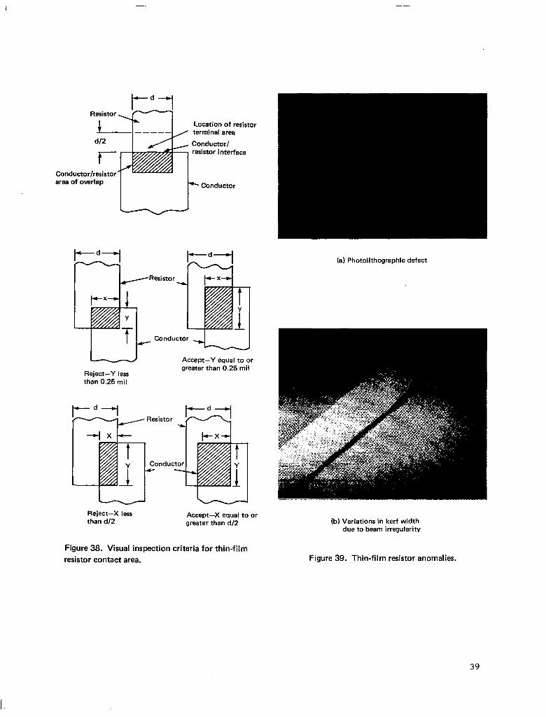
Photolithographic errors can cause excess thin-film material to be left on the die (fig. 39a). In the extreme case, the extra material could contact other active
38
Figure 37. Semiconductor dice that have attached portions of the active circuit areas of other dice.
Location of resistor terminal area
resistor interface
Conductor/resistor area of overlap
Reject-Y less than 0.25 mil
I-d-i P -d-l Resistor 7
I-”
Kf P-x
V
f Conductor -L-
I Accept-Y equal to or greater than 0.25 mil
w Resistor m
ndu
Reject-X less than d/2
Accept-X equal to or greater than d/2
Figure 38. Visual inspection criteria for thin-film resistor contact area.
(a) Photolithographic defect
(b) Variations in kerf width due to beam irregularity
Figure 39. Thin-film resistor anomalies.
39
circuit areas. A thin-film resistor is unacceptable if it has an increase greater than 25 percent of the origi- nal width or if the separation between resistors or a resistor and a metallization path is less than 0.25 mil.
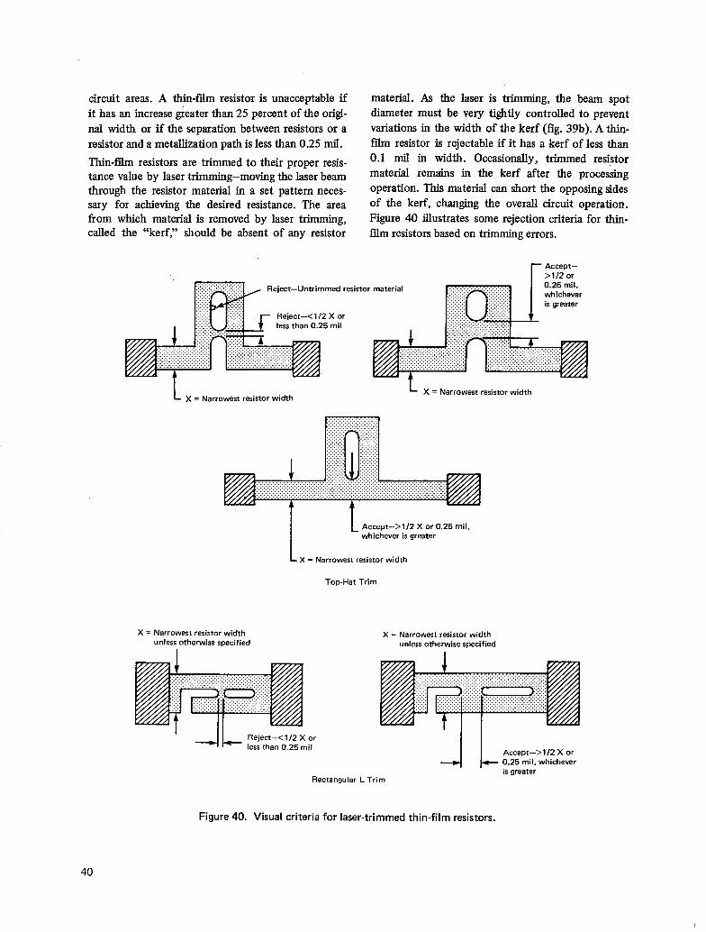
?hin&lm resistors are trimmed to their proper resis- tance value by laser trimming-moving the laser beam through the resistor material in a set pattern neces- sary for achieving the desired resistance. The area from which material is removed by laser trimming, called the “kerf,” should be absent of any resistor
Reject-Untrimmed I
Reject-<1 I2 X or less than 0.25 mil
material. As the laser is trimming, the beam spot diameter must be very tightly controlled to prevent variations in the width of the kerf (fig. 39b). A thin- !Tilm resistor is rejectable if it has a kerf of less than 0.1 mil in width. Occasionally, trimmed resistor material remains in the kerf after the processing operation. This material can short the opposing sides of the kerf, changing the overall circuit operation. Figure 40 illustrates some rejection criteria for thin- film resistors based on trimming errors.
r Accept- >1/2 or
x = Narrowest resistor width X = Narrowest resistor
Accept->112 X or 0.25 mil, whichever is greater
X = Narrowest resistor width
Top-Hat Trim
X = Narrowest resistor width X = Narrowest resistor width unless otherwise specified unless otherwise specified
or less than 0.25 mil Accept->112 X or
Rectangular L Trim
4 k 0.25 mil, whichever is greater
Figure 40. Visual criteria for laser-trimmed thin-film resistors.
40
Wire Bonding
In integrated circuits, wire bonds are common sources of failure, particularly the bonds on the die. It is therefore important to pay close attention to the bonds during precap visual examinations. Several criteria are important to the reliability of gold ball bonds. The first is the size of the bond. The bond should not be less than 2 times, nor greater than 5 times, the wire diameter (fig. 41). When the bond is less than 2 times the wire diameter, not enough area of the ball is bonded to the metallization pad. In addition, when the bond is too small, a phenomenon called “cratering” can occur. Cratering is a fracture in the silicon substrate under the bond that results from the impact of the hard bonding tool (fig. 42). If the bond is greater than 5 times the wire diameter, the ball bond can overlap the metallization bonding pad. As integrated circuits become more dense, the size of the bonding pads decrease; currently they are on the order of 4 mils square. When ball bonds overlap the pad, the glassivation can crack. Cracking of the glassi- vation could be a reliability hazard if excessive mois- ture is present in the package. If the ball bond size falls between 2 and 5 times the wire diameter, the bond will probably be good. However, the ball size is sometimes visually acceptable even though an underbond has occurred.
An underbond occurs where insufficient heat and/or bonding pressure has been applied during bonding, and the ball is only tacked on although its appearance is visually acceptable. To detect this type of bond, more than a visual inspection is required. One way of detecting bonds of this type (although it is outside the scope of a precap examination) is to use a non- destructive wire bond pull test (NDP). The intent of this test is to use a force great enough to cause weak bonds to fail, but not great enough to damage good bonds. However, when using the NDP test, variables such as wire and bond-loop elongation, bond geom- etry, and the mean and the standard deviation of the destructive bond pull test must be considered in de- vising safe nondestructive wire bond pull force limits. Harman and Cannon (1978) summarized the recom- mended NDP force limits. An alternative to the NDP test is to subject the device to mechanical shock or vibration screening. These tests are performed to work the bond loose, usually after package sealing.
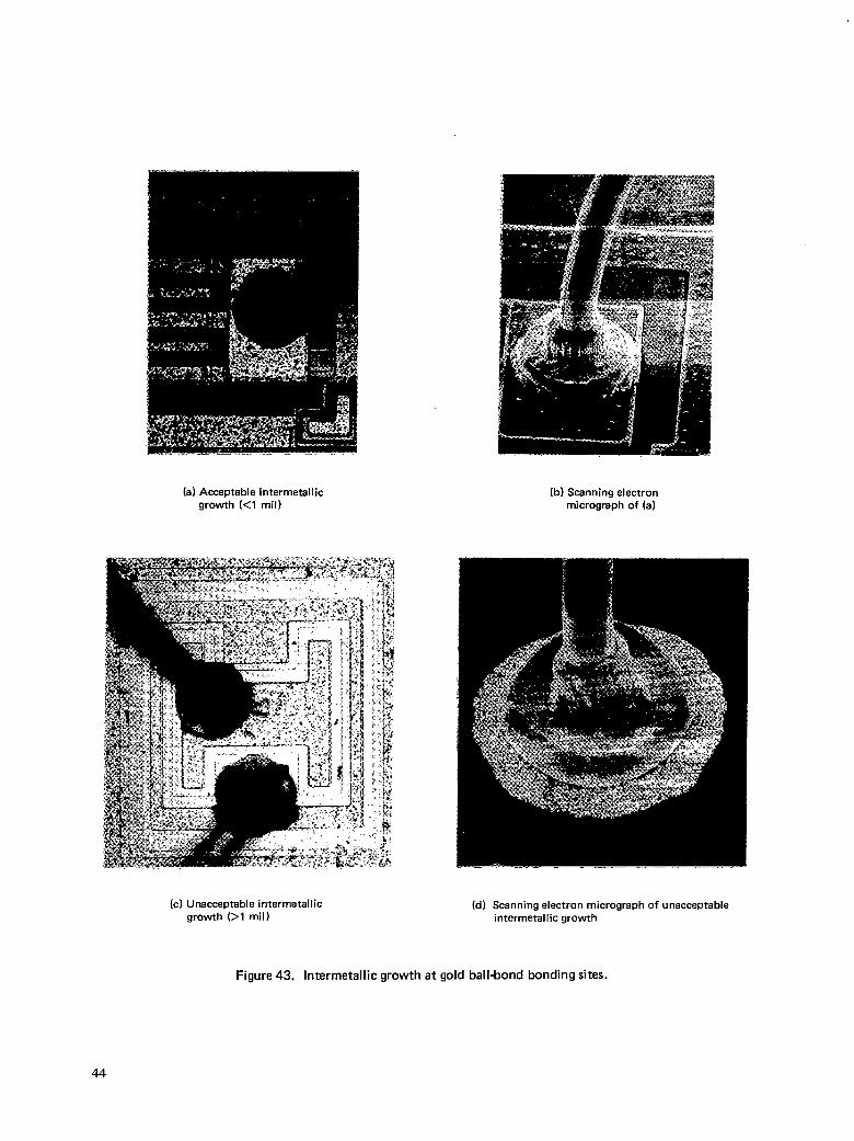
When inspecting gold ball bonds that are bonded in bimetallic systems (usually gold/aluminum), it is important to examine the bond for inter-metallic growth (fig. 43). According to MIL-STD-883B, Method 2010, condition A, a bond is unacceptable if it exhibits inter-metallic formation that extends radially more than 0.1 mil completely around the periphery of any gold ball bond for that portion of the bond located .on metal. Gold/aluminum inter- metallic compound formations have been studied extensively. These compounds may form during thermocompression bonding, during subsequent qualifying thermal screens, and during storage of the device if the temperature is 2OO’C (475 K) or higher. The fact that intermetallic formations can occur at any time in the life of a device when high tempera- tures are encountered does not mean that the bond will necessarily degrade either electrically or mechan- ically. It was originally assumed that any bond with intermetallic compounds was bad. Only after exten- sive study was it found that metallurgical (Kirkendall) voids actually caused the failures rather than the intermetallic compounds.
Two types of void-induced bond failures have been observed. In the first failure type, the bond can be mechanically strong, but it can have a high electrical resistance or even be open circuited. This type of failure occurs when voids form around the bond periphery, limiting the current carrying area of the bonding pad metallization. In the second type of failure, the voids in the metallization occur under- neath the bond. This type of bond fails because of mechanical weakness.
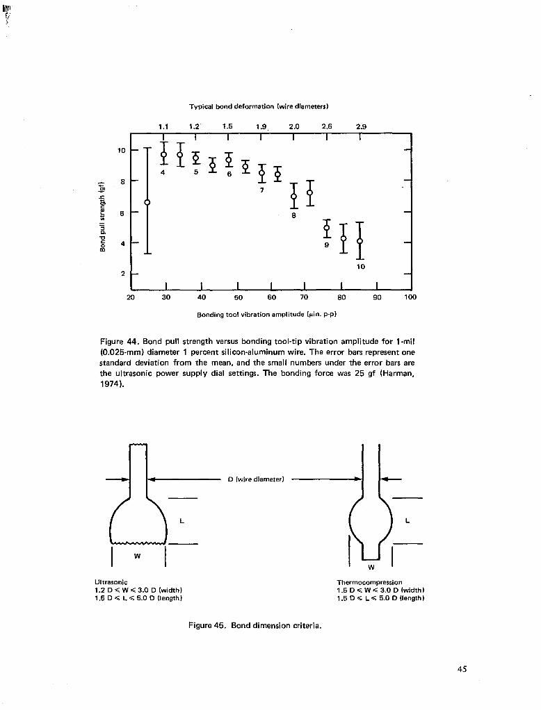
Wedge bonds are judged on a different basis as far as the criteria relating to wire size is concerned. Ultra- sonic wedge bonds are considered unacceptable if the bond is less than 1.2 times, or greater than 3 times, the wire diameter in width. If the bond is less than 1.2 times the wire diameter, a large variability in the pull strength results as shown in figure 44. Bonds less than 1.2 times the wire diameter are susceptible to contamination on the surface of the bonding pads. Ultrasonic wedge bonds of less than 1.2 wire diameters result from a combination of insufficient bonding tool vibration amplitude and force so that the surface contaminants are not broken up and properly swept
41
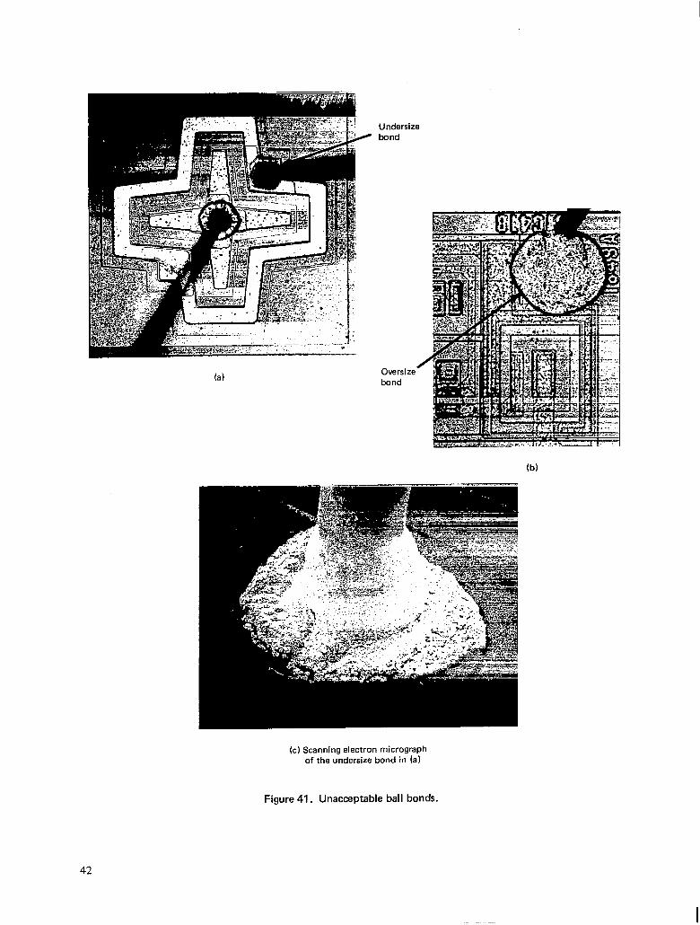
Undersize bond
(a) Oversize bond
(b)
(c) Scanning electron micrograph of the undersize bond in (a)
Figure 41. Unacceptable ball bonds.
42
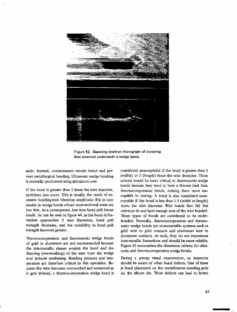
Figure 42. Scanning electron micrograph of cratering that occurred underneath a wedge bond.
aside. Instead, contaminants remain intact and pre- vent metallurgical bonding. Ultrasonic wedge bonding is normally performed using aluminum wire.
If the bond is greater than 3 times the wire diameter, problems also occur. This is usually the result of ex- cessive bonding-tool vibration amplitude; this in turn results in wedge bonds whose cross-sectional areas are too thin. As a consequence, low wire bond pull forces result. As can be seen in figure 44, as the bond defor- mation approaches 3 wire diameters, bond pull strength decreases, and the variability in bond pull strength becomes greater. .
Thermocompression and thermosonic wedge bonds of gold to aluminum are not recommended because the intermetallic phases weaken the bond and the thinning (overworking) of the wire from the wedge tool induces weakening. Bonding pressure and tem- perature are therefore critical in this operation. Be- cause the wire becomes overworked and weakened as it gets thinner, a thermocompression wedge bond is
considered unacceptable if the bond is greater than 3 (width) or 5 (length) times the wire diameter. These criteria would be more critical in thermosonic wedge bonds because they tend to have a thinner heel than thermocompression bonds, making them more sus- ceptible to tearing. A bond is also considered unac- ceptable if the bond is less than 1.5 (width or length) times the wire diameter. Wire bonds that fail this criterion do not have enough area of the wire bonded. These types of bonds are considered to be under- bonded. Normally, thermocompression and thermo- sonic wedge bonds are monometallic systems such as gold wire to gold contacts and aluminum wire to aluminum contacts. As such, they do not experience intermetallic formations and should be more reliable. Figure 45 summarizes the dimension criteria for ultra- sonic and thermocompression wedge bonds.
During a precap visual examination, an inspector should be aware of other bond defects. One of these is bond placement on the metallization bonding pads on the silicon die. These defects can lead to latent
43
(a) Acceptable intermetallic growth (<l mill
(b) Scanning electron micrograph of (a)
ICI Unacceptable intermetallic growth (>l mil)
(d) Scanning electron micrograph of unacceptable intermetallic growth
Figure 43. Intermetallic growth at gold ball-bond bonding sites.
44
c
Typical bond deformation (wire diameters)
P 7
P 8
20 30 40 50 60 70 80
Bonding tool vibration amplitude (pin. P-P)
90 100
Figure 44. Bond pull strength versus bonding tool-tip vibration amplitude for I-mil (0.025-mm) diameter 1 percent silicon-aluminum wire. The error bars represent one standard deviation from the mean, and the small numbers under the error bars are the ultrasonic power supply dial settings. The bonding force was 25 gf (Harman, 1974).
0 (wire diameter) w -
W I
Ultrasonic Thermocompression 1.2 D < W Q 3.0 D (width) 1.5 D C W G 3.0 D (width) 1.5 D < L < 5.0 D (length) 1.5 D < L < 5.0 D (length)
Figure 45. Bond dimension criteria.
4.5
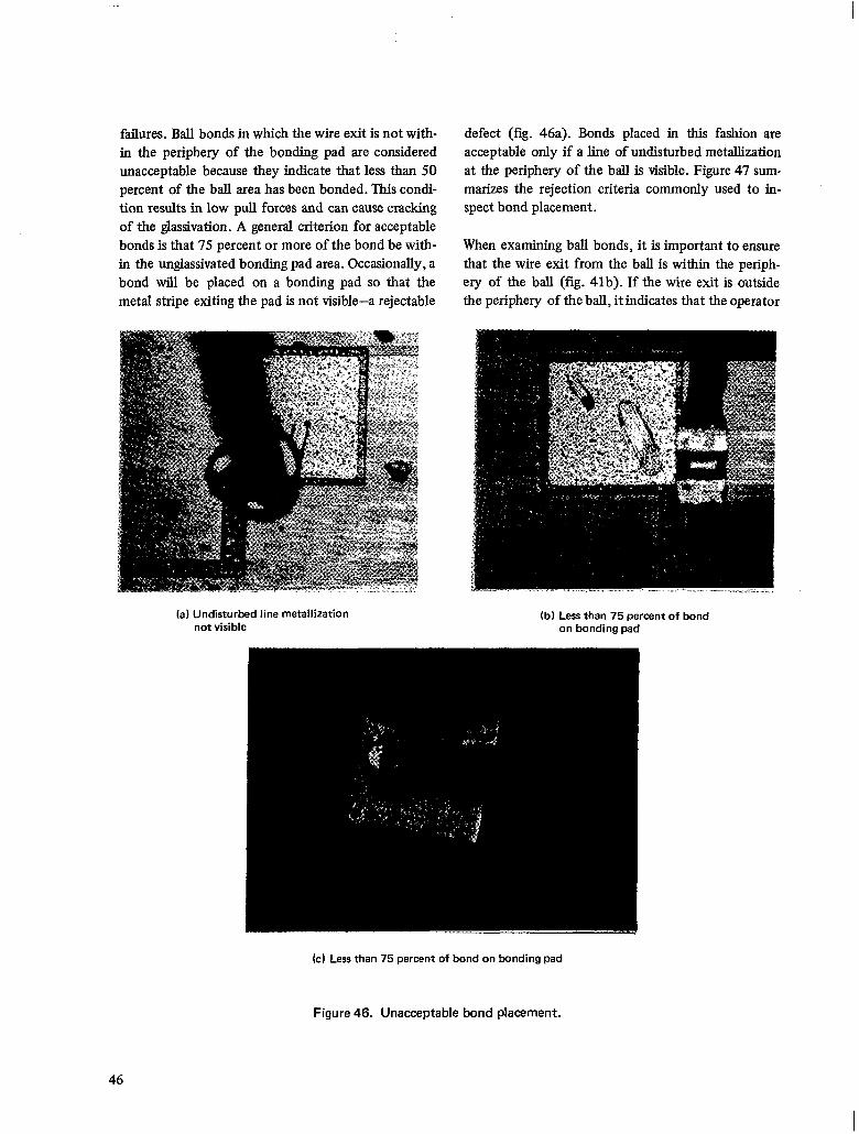
failures. Ball bonds in which the wire exit is not with- in the periphery of the bonding pad are considered unacceptable because they indicate that less than 50 percent of the ball area has been bonded. This condi- tion results in low pull forces and can cause cracking of the glassivation. A general criterion for acceptable bonds is that 75 percent or more of the bond be with- in the unglassivated bonding pad area. Occasionally, a bond will be placed on a bonding pad so that the metal stripe exiting the pad is not visible-a rejectable
defect (fig. 46a). Bonds placed in this fashion are acceptable only if a line of undisturbed metallization at the periphery of the ball is visible. Figure 47 sum- marizes the rejection criteria commonly used to in- spect bond placement.
When examining ball bonds, it is important to ensure that the wire exit from the ball is within the periph- ery of the ball (fig. 41b). If the wire exit is outside the periphery of the ball, it indicates that the operator
(a) Undisturbed line metallization not visible
(b) Less than 75 percent of bond on bonding pad
(c) Less than 75 percent of bond on bonding pad
Figure 46. Unacceptable bond placement.
46
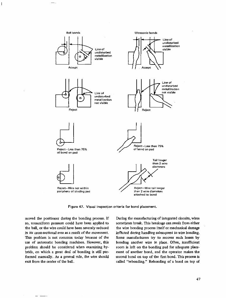
Ball bonds I da Line of
0
undisturbed metallization visible
Reject
iJ Reject-Less than 75% of bond on pad
d 0
Reject-Wire not within periphery of binding pad
Line of undisturbed metallization not visible
Ultrasonic bonds
undisturbed metallization
undisturbed metallization
Reject-Less than 75% of bond on pad
Tail longer than 2 wire
Reject-Wire tail longer than 2 wire diameters attached to bond
Figure 47. Visual inspection criteria for bond placement.
moved the positioner during the bonding process. If so, nonuniform pressure could have been applied to the ball, or the wire could have been severely reduced in its cross-sectional area as a result of the movement. This problem is not common today because of the use of automatic bonding machines. However, this problem should be considered when examining hy- brids, on which a great deaI of bonding is still per- formed manually. As a general rule, the wire should exit from the center of the ball.
During the manufacturing of integrated circuits, wires sometimes break. This breakage can result from either the wire bonding process itself or mechanical damage inflicted during handling subsequent to wire bonding. Some manufacturers try to recover such losses by bonding another wire in place. Often, insufficient room is left on the bonding pad for adequate place- ment of another bond, and the operator makes the second bond on top of the fust bond. This process is called “rebonding.” Rebonding of a bond on top of
47
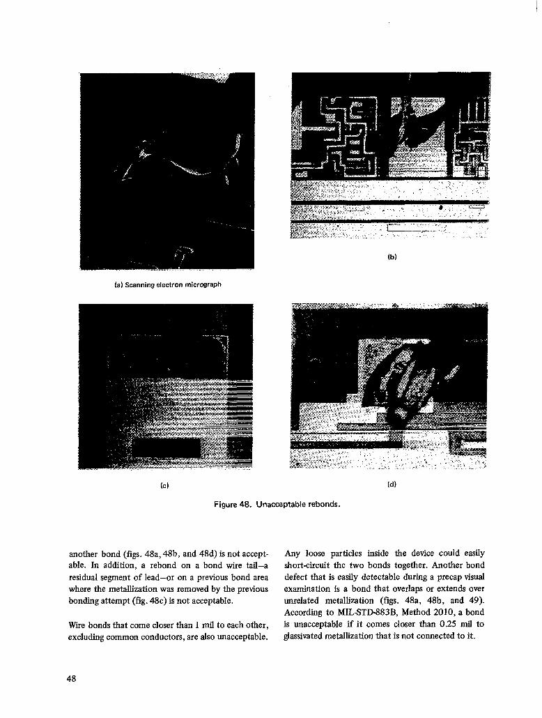
(a) Scanning electron micrograph
(cl (d)
Figure 48. Unacceptable rebonds.
another bond (figs. 48a, 48b, and 48d) is not accept- Any loose particles inside the device could easily able. In addition, a rebond on a bond wire tail-a short-circuit the two bonds together. Another bond residual segment of lead-or on a previous bond area defect that is easily detectable during a precap visual where the metallization was removed by the previous examination is a bond that overlaps or extends over bonding attempt (fig. 48~) is not acceptable. unrelated metallization (figs. 48a, 48b, and 49).
According to MIL-STD883B, Method 2010, a bond Wire bonds that come closer than 1 mil to each other, is unacceptable if it comes closer than 0.25 mil to excluding common conductors, are also unacceptable. glassivated metallization that is not connected to it.
48
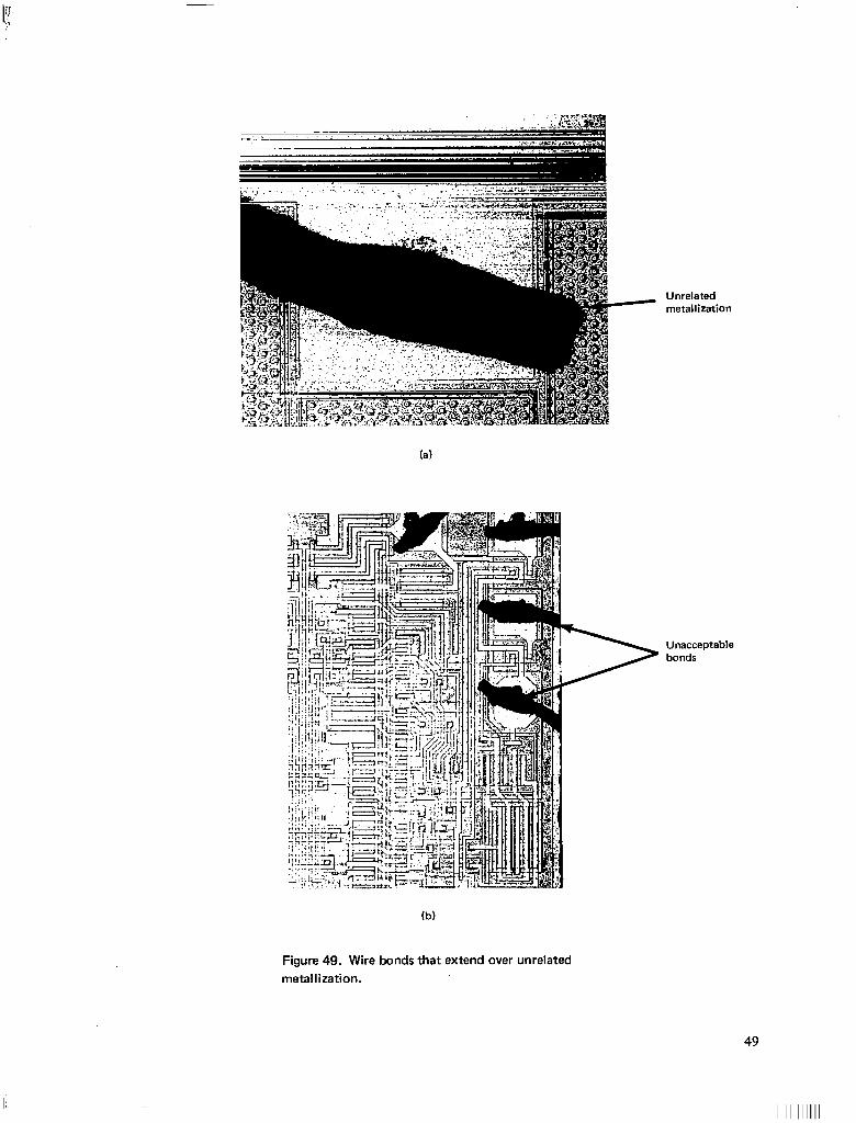
Unrelated metallization
Unacceptable bonds
(b)
Figure 49. Wire bonds that extend over unrelated metallization.
49
I I I II I II llllll I
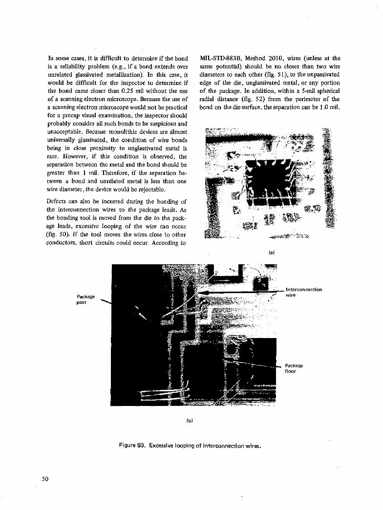
In some cases, it is difficult to determine if the bond is a reliability problem (e.g., if a bond extends over unrelated glassivated metallization). In this case, it would be difficult for the inspector to determine if the bond came closer than 0.25 mil without the use of a scanning electron microscope. Because the use of a scanning electron microscope would not be practical for a precap visual examination, the inspector should probably consider all such bonds to be suspicious and unacceptable. Because monolithic devices are almost universally glassivated, the condition of wire bonds being in close proximity to unglassivated metal is rare. However, if this condition is observed, the separation between the metal and the bond should be greater than 1 mil. Therefore, if the separation be- tween a bond and unrelated metal is less than one wire diameter, the device would be rejectable.
Defects can also be incurred during the bonding of the interconnection wires to the package leads. As the bonding tool is moved from the die to the pack- age leads, excessive looping of the wire can occur (fig. 50). If the tool moves the wires close to other conductors, short circuits could occur. According to
Package
MIL-STD-883B, Method 2010, wires (unless at the same potential) should be no closer than two wire diameters to each other (fig. 51), to the unpassivated edge of the die, unglassivated metal, or any portion of the package. In addition, within a 5-mil spherical radial distance (fig. 52) from the perimeter of the bond on the die surface, the separation can be 1 .O mil.
(a)
. Interconnection wire
Package floor
(b)
Figure 50. Excessive looping of interconnection wires.
50

Unacceptable (<2 wire diameters)
TOD
Figure 51. Interconnection wires passing within 2
wire diameters of each other.
Edge of die 5-mil sphere
5-mil radial distance
/ Wire must clear this point
5-mils I+
t
from Package floor
heel of bond
Side
(a) Criteria for spherical radial distance
Figure 52. Criteria concerning wire clearance.
51
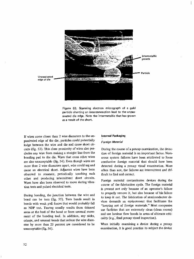
Unpassivated edge of die
Figure 53. Scanning electron micrograph of a gold particle shorting an interconnection lead to the unpas- sivated die edge. Note the intermetallic that has grown as a result of the short.
If wires come closer than 2 wire diameters to the un- passivated edge of the die, particles could potentially lodge between the wire and die and cause short cir- cuits (fig. 53). This close proximity of wires also pre- cludes any wire from making a straight line from the bonding pad to the die. Wires that cross other wires are also unacceptable (fig. 54). Even though wires are more than 2 wire diameters apart, wire could sag and cause an electrical short. Adjacent wires have been observed to resonate, periodically touching each other and producing intermittent short circuits. Wires have also been observed to move during vibra- tion tests and pulsed electrical tests.
During bonding, the junction between the wire and bond can be torn (fig. 55). Torn bonds result in bonds with weak pull forces that would probably fail an NDP test. Tearing usually results from thinned areas at the heel of the bond or from unusual move- ment of the bonding tool. In addition, any nicks, crimps, and unusual bends that reduce the wire diam- eter by more than 25 percent are considered to be unacceptable (fig. 56).
, Intermetallic growth
Particle
Internal Packaging
Foreign Material
During the course of a precap examination, the detec- tion of foreign material is an important factor. Num- erous system failures have been attributed to loose conductive foreign material that should have been detected during a precap visual examination. More often than not, the failures are intermittent and dif- ficult to find and correct.
Foreign material contaminates devices during the course of the fabrication cycle. The foreign material is present not only because of an operator’s failure to properly remove it, but also because of his failure to keep it out. The fabrication of semiconductor de- vices demands an environment that facilitates the “keeping out of foreign materials.” Most companies use facilities that are extremely clean (clean rooms) and use laminar flow hoods in areas of ultimate criti- cality (e.g.; final precap visual inspection).
When initially examining a device during a precap examination, it is good practice to subject the device
52
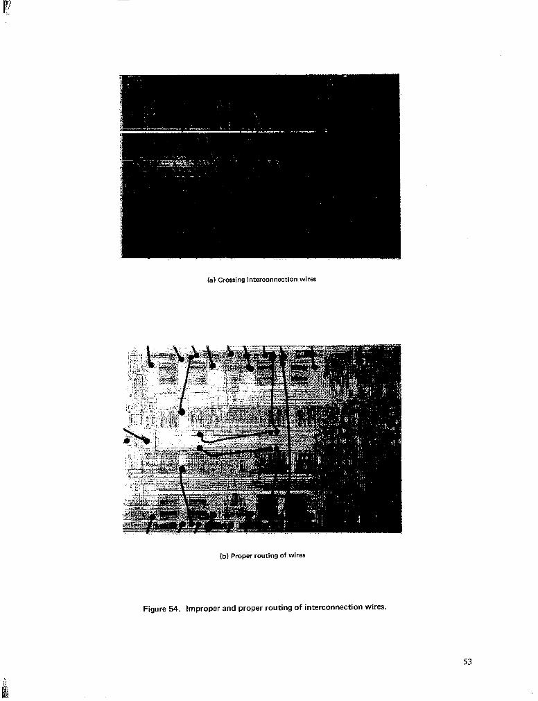
(a) Crossing interconnection wires
(b) Proper routing of wires
Figure 54. Improper and proper routing of interconnection wires.
53
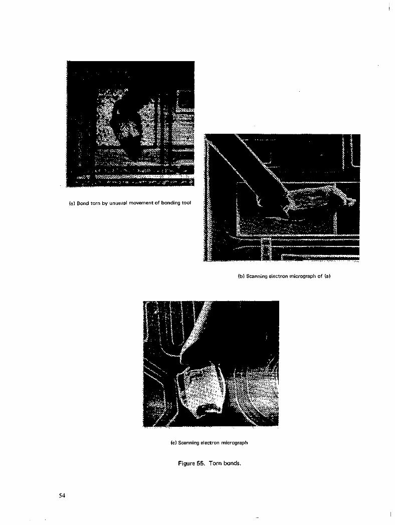
--_-I^
(a) Bond torn by unusual movement of bonding tool
(b) Scanning electron micrograph of (a)
(c) Scanning electron micrograph
Figure 55. Torn bonds.
54
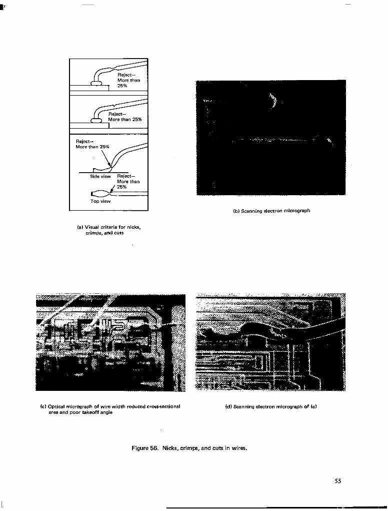
More than 2596, I
Reject- More than 25%
-4 Side view Reject-
More than
(b) Scanning electron micrograph
(a) Visual criteria for nicks, crimps, and cuts
(cl Optical micrograph of wire width reduced crosssectional area and poor takeoff angle
(d) Scanning electron micrograph of (c)
Figure 56. Nicks, crimps, and cuts in wires.
55
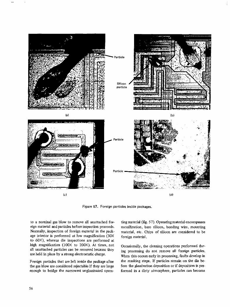
(a) (b)
0 Particle
Particle
Figure 57. Foreign particles inside packages.
to a nominal gas blow to remove all unattached for- eign material and particles before inspection proceeds. Normally, inspection of foreign material in the pack- age interior is performed at low magnification (30X to 60X), whereas die inspections are performed at high magnification (100X to 200X). At times, not all unattached particles can be removed because they are held in place by a strong electrostatic charge.
Foreign particles that are left inside the package after the gas blow are considered rejectable if they are large enough to bridge the narrowest unglassivated opera-
ting material (fig. 57). Operating material encompasses metallization, bare silicon, bonding wire, mounting material, etc. Chips of silicon are considered to be foreign material.
Occasionally, the cleaning operations performed dur- ing processing do not remove all foreign particles. When this occurs early in processing, faults develop in the masking steps. If particles remain on the die be- fore the glassivation deposition or if deposition is per- formed in a dirty atmosphere, particles can become
56
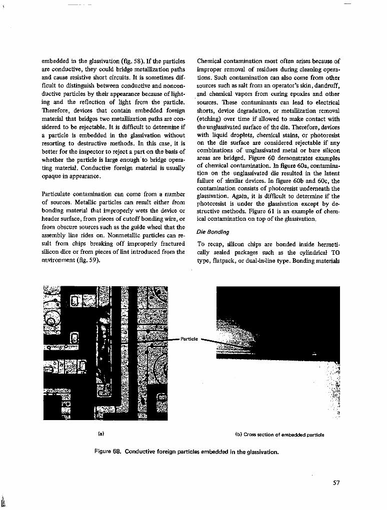
embedded in the glassivation (fig. 58). If the particles are conductive, they could bridge metalhzation paths and cause resistive short circuits. It is sometimes dif- ficult to distinguish between conductive and noncon- ductive particles by their appearance because of light- ing and the reflection of light from the particle. Therefore, devices that contain embedded foreign material that bridges two metallization paths are con- sidered to be rejectable. It is difficult to determine if a particle is embedded in the glasslvation without resorting to destructive methods. In this case, it is better for the inspector to reject a part on the basis of whether the particle is large enough.to bridge opera- ting material. Conductive foreign material is usually opaque in appearance.
Particulate contamination can come from a number of sources. Metallic particles can result either from bonding material that improperly wets the device or header surface, from pieces of cutoff bonding wire, or from obscure sources such as the guide wheel that the assembly line rides on. Nonmetallic particles can re- sult from chips breaking off improperly fractured silicon dice or from pieces of lint introduced from the environment (fig. 59).
Chemical contamination most often arises because of improper removal of residues during cleaning opera- tions. Such contamination can also come from other sources such as salt from an operator’s skin, dandruff, and chemical vapors from curing epoxies and other sources. These contaminants can lead to electrical shorts, device degradation, or metallization removal (etching) over time if allowed to make contact with the unglassivated surface of the die. Therefore, devices with liquid droplets, chemical stains, or photoresist on the die surface are considered rejectable if any combinations of unglassivated metal or bare silicon areas are bridged. Figure 60 demonstrates examples of chemical contamination. In figure 60a, contamina- tion on the unglassivated die resulted in the latent failure of similar devices. In figure 60b and 6Oc, the contamination consists of photoresist underneath the glassivation. Again, it is difficult to determine if the photoresist is under the glassivation except by de- structive methods. Figure 61 is an example of chem- ical contamination on top of the glassivation.
Die Bonding
To recap, silicon chips are bonded inside hermeti- cally sealed packages such as the cylindrical TO type, flatpack, or dual-in-line type. Bonding materials
m Particle
(a) (b) Cross section of embedded particle
Figure 58. Conductive foreign particles embedded in the glassivation.
57
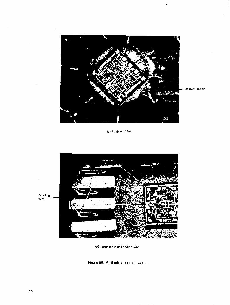
Contamination
(a) Particle of lint
Bonding wire
(b) Loose piece of bonding wire
Figure 59. Particulate contamination.
58
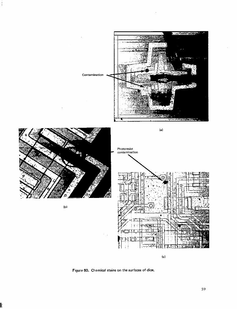
Contamination
Photoresist contamination
(a)
Figure 60. Chemical stains on the surfaces of dice.
59
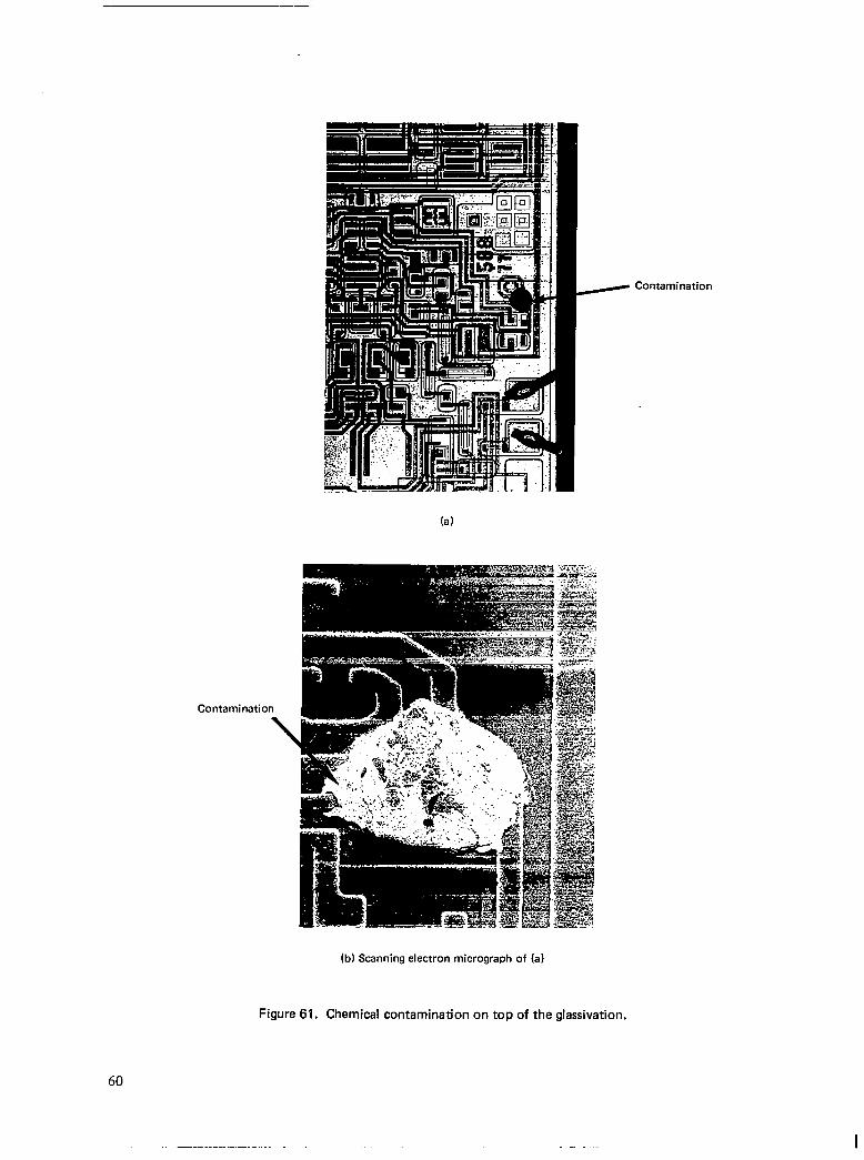
(a)
Contamination
- Contamination
(b) Scanning electron micrograph of (a)
Figure 61. Chemical contamination on top of the glassivation.
60
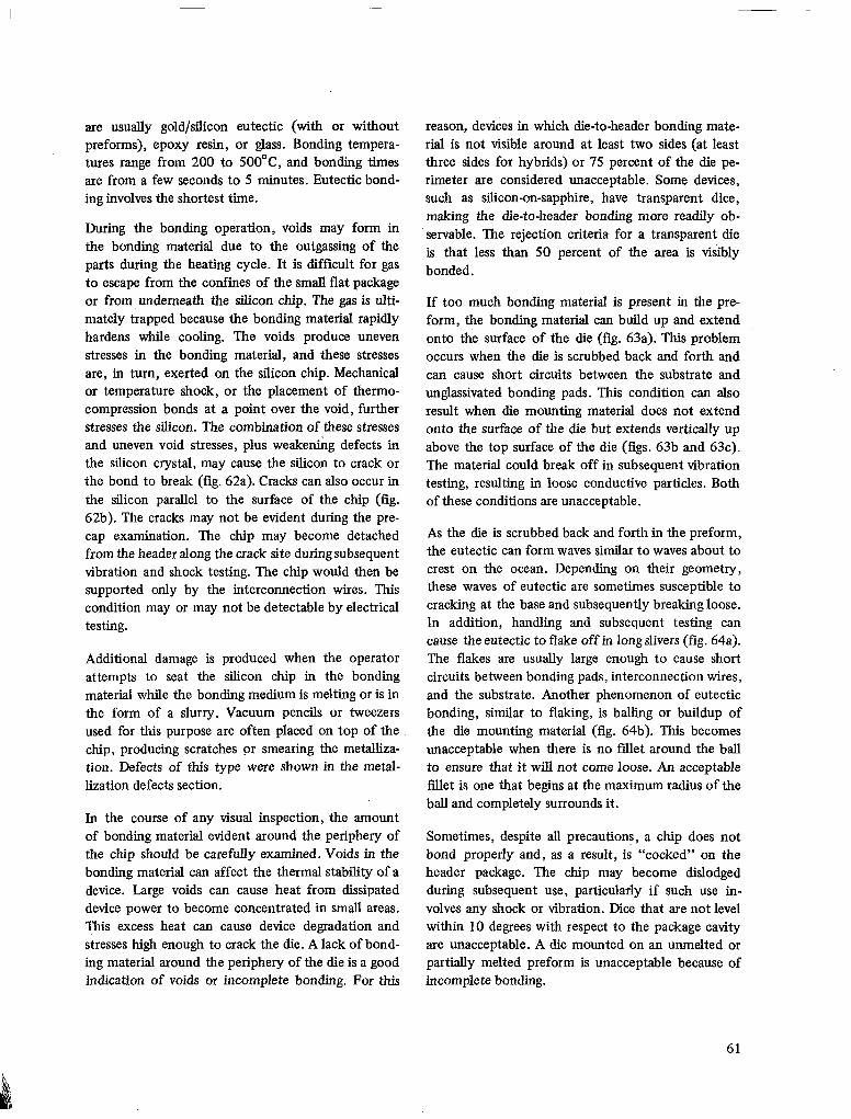
are usually gold/silicon eutectic (with or without preforms), epoxy resin, or glass. Bonding tempera- tures range from 200 to 500eC, and bonding times are from a few seconds to 5 minutes. Eutectic bond- ing involves the shortest time.
During the bonding operation, voids may form in the bonding material due to the outgassing of the parts during the heating cycle. It is difficult for gas to escape from the confines of the small flat package or from underneath the silicon chip. The gas is ulti- mately trapped because the bonding material rapidly hardens while cooling. The voids produce uneven stresses in the bonding material, and these stresses are, in turn, exerted on the silicon chip. Mechanical or temperature shock, or the placement of thermo- compression bonds at a point over the void, further stresses the silicon. The combination of these stresses and uneven void stresses, plus weakening defects in the silicon crystal, may cause the silicon to crack or the bond to break (fig. 62a). Cracks can also occur in the silicon parallel to the surface of the chip (fig. 62b). The cracks may not be evident during the pre- cap examination. The chip may become detached from the header along the crack site during subsequent vibration and shock testing. The chip would then be supported only by the interconnection wires. This condition may or may not be detectable by electrical testing.
Additional damage is produced when the operator attempts to seat the silicon chip in the bonding material while the bonding medium is melting or is in the form of a slurry. Vacuum pencils or tweezers used for this purpose are often placed on top of the chip, producing scratches or smearing the metalliza- tion. Defects of this type were shown in the metal- lization defects section.
In the course of any visual inspection, the amount of bonding material evident around the periphery of the chip should be carefully examined. Voids in the bonding material can affect the thermal stability of a device. Large voids can cause heat from dissipated device power to become concentrated in small areas. This excess heat can cause device degradation and stresses high enough to crack the die. A lack of bond- ing material around the periphery of the die is a good indication of voids or incomplete bonding. For this
reason, devices in which die-to-header bonding mate- rial is not visible around at least two sides (at least three sides for hybrids) or 75 percent of the die pe- rimeter are considered unacceptable. Some devices, such as silicon-on-sapphire, have transparent dice, making the die-to-header bonding more readily ob- servable. The rejection criteria for a transparent die is that less than 50 percent of the area is viiibly bonded,
If too much bonding material is present in the pre- form, the bonding material can build up and extend onto the surface of the die (fig. 63a). This problem occurs when the die is scrubbed back and forth and can cause short circuits between the substrate and unglassivated bonding pads. This condition can also result when die mounting material does not extend onto the surface of the die but extends vertically up above the top surface of the die (figs. 63b and 63~). The material could break off in subsequent vibration testing, resulting in loose conductive particles. Both of these conditions are unacceptable.
As the die is scrubbed back and forth in the preform, the eutectic can form waves similar to waves about to crest on the ocean. Depending on their geometry, these waves of eutectic are sometimes susceptible to cracking at the base and subsequently breaking loose. In addition, handling and subsequent testing can cause the eutectic to flake off in long slivers (fig. 64a). The flakes are usually large enough to cause short circuits between bonding pads, interconnection wires, and the substrate. Another phenomenon of eutectic bonding, similar to flaking, is balling or buildup of the die mounting material (fig. 64b). This becomes unacceptable when there is no fillet around the ball to ensure that it will not come loose. An acceptable fillet is one that begins at the maximum radius of the ball and completely surrounds it.
Sometimes, despite all precautions, a chip does not bond properly and, as a result, is “cocked” on the header package. The chip may become dislodged during subsequent use, particularly if such use in- volves any shock or vibration. Dice that are not level within 10 degrees with respect to the package cavity are unacceptable. A die mounted on an unmelted or partially melted preform is unacceptable because of incomplete bonding.
61
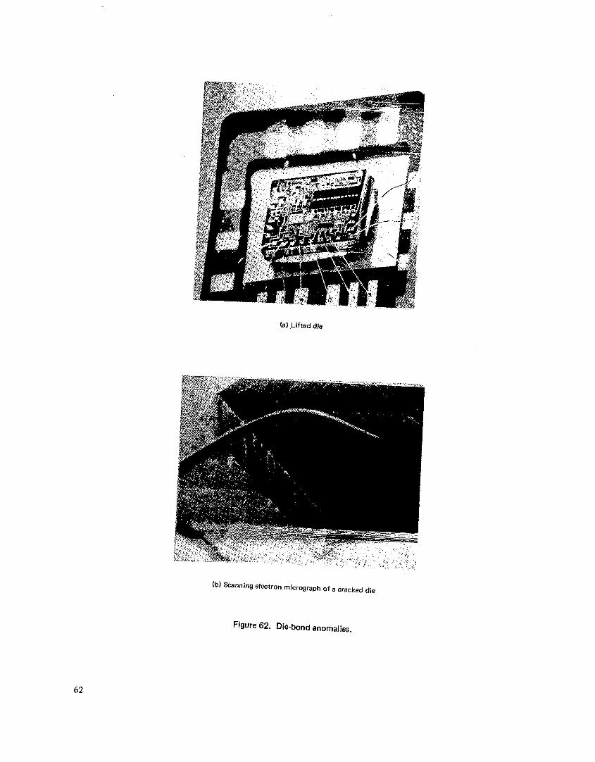
lb) bmning electron micrograph of a cracked die
Figure 62. Die-bond anomalies.
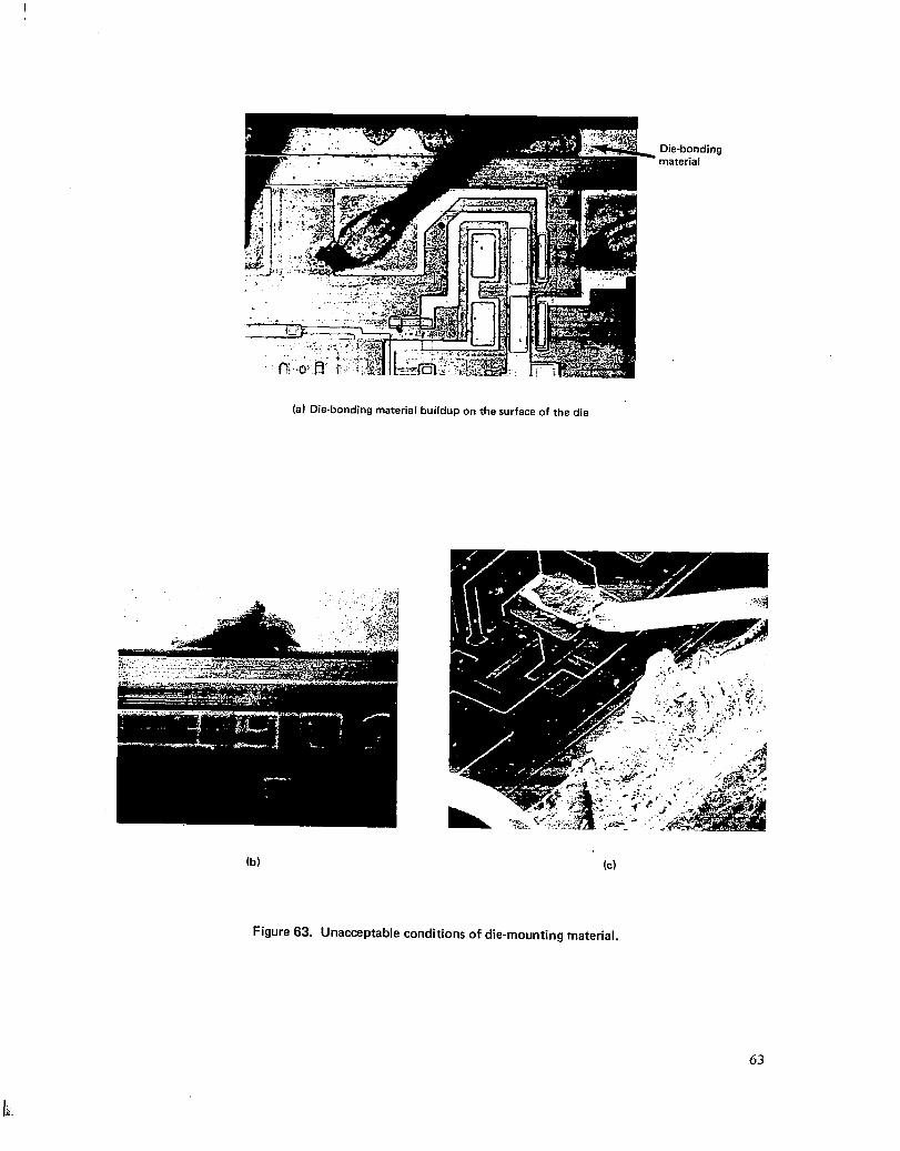
Die-bonding material
(a) Die-bonding material buildup on the surface of the die
(b) (c)
Figure 63. Unacceptable COI nditions of die-mounting material.
63
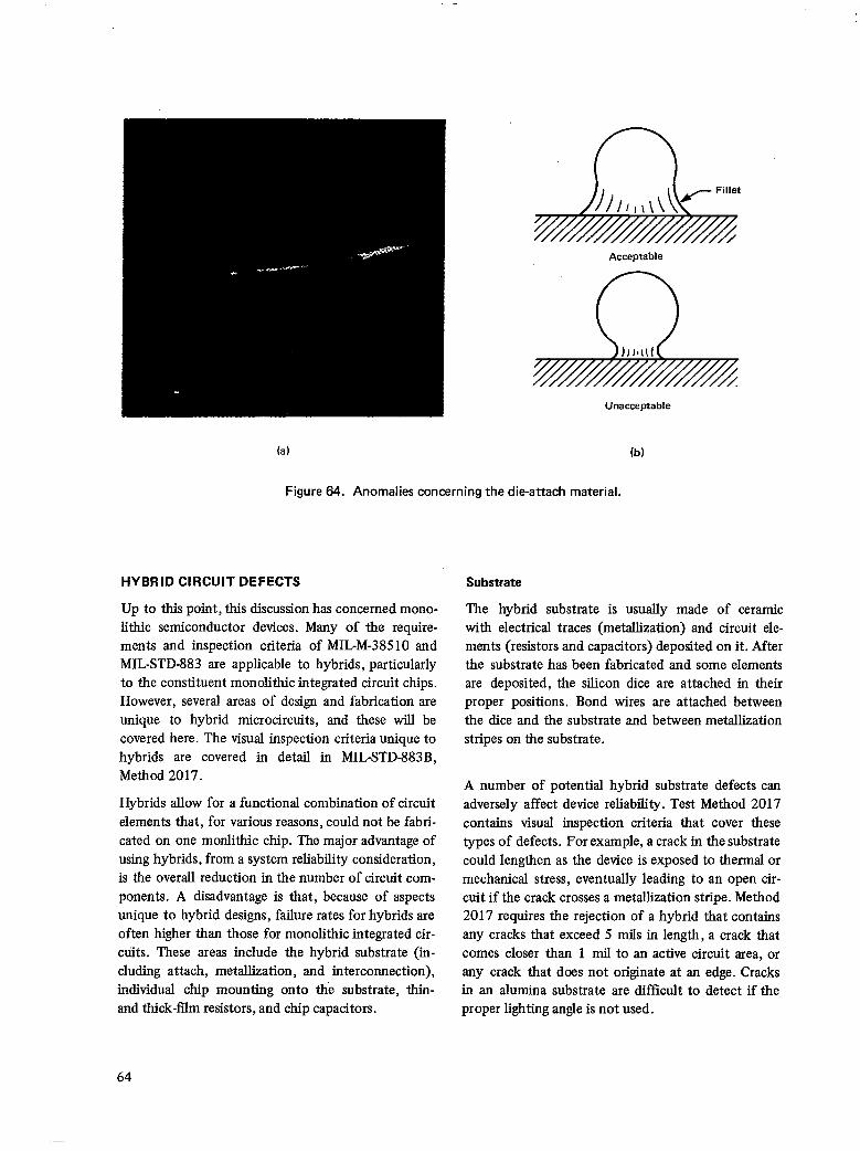
Acceptable
Unacceptable
(al lb)
Figure 64. Anomalies concerning the die-attach material.
HYBRID CIRCUIT DEFECTS Substrate
Up to this point, this discussion has concerned mono- lithic semiconductor devices. Many of the require- ments and inspection criteria of MIL-M-38510 and MIL-STD-883 are applicable to hybrids, particularly to the constituent monolithic integrated circuit chips. However, several areas of design and fabrication are unique to hybrid microcircuits, and these will be covered here. The visual inspection criteria unique to hybrids are covered in detail in MILSTD883B, Method 2017.
The hybrid substrate is usually made of ceramic with electrical traces (metallization) and circuit ele- ments (resistors and capacitors) deposited on it. After the substrate has been fabricated and some elements are deposited, the silicon dice are attached in their proper positions. Bond wires are attached between the dice and the substrate and between metallization stripes on the substrate.
Hybrids allow for a functional combination of circuit elements that, for various reasons, could not be fabri- cated on one monlithic chip. The major advantage of using hybrids, from a system reliability consideration, is the overall reduction in the number of circuit com- ponents. A disadvantage is that, because of aspects unique to hybrid designs, failure rates for hybrids are often higher than those for monolithic integrated cir- cuits. These areas include the hybrid substrate (in- cluding attach, metallization, and interconnection), individual chip mounting onto the substrate, thin- and thick-film resistors, and chip capacitors.
A number of potential hybrid substrate defects can adversely affect device reliability. Test Method 2017 contains visual inspection criteria that cover these types of defects. For example, a crack in the substrate could lengthen as the device is exposed to thermal or mechanical stress, eventually leading to an open cir- cuit if the crack crosses a metallization stripe. Method 2017 requires the rejection of a hybrid that contains any cracks that exceed 5 mils in length, a crack that comes closer than 1 mil to an active circuit area, or any crack that does not originate at an edge. Cracks in an alumina substrate are difficult to detect if the proper lighting angle is not used.
64
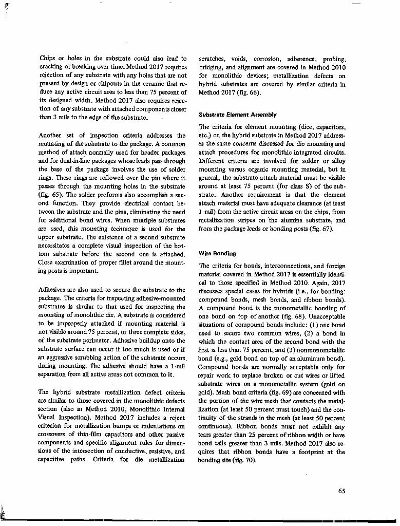
Chips or holes in the substrate could also lead to cracking or breaking over time. Method 20 17 requires rejection of any substrate with any holes that are not present by design or chipouts in the ceramic that re- duce any active circuit area to less than 75 percent of its designed width. Method 2017 also requires rejec- tion of any substrate with attached components closer than 3 mils to the edge of the substrate.
Another set of inspection criteria addresses the mounting of the substrate to the package. A common method of attach normally used for header packages and for dual-in-line packages whose leads pass through the base of the package involves the use of solder rings. These rings are reflowed over the pin where it passes through the mounting holes in the substrate (fig. 65). The solder preforms also accomplish a sec- ond function. They provide electrical contact be- tween the substrate and the pins, eliminating the need for additional bond wires. When multiple substrates are used, this mounting technique is used for the upper substrate. The existence of a second substrate necessitates a complete visual inspection of the bot- tom substrate before the second one is attached. Close examination of proper fillet around the mount- ing posts is important.
Adhesives are also used to secure the substrate to the package. The criteria for inspecting adhesive-mounted substrates is similar to that used for inspecting the mounting of monolithic die. A substrate is considered to be improperly attached if mounting material is not visible around 75 percent, or three complete sides, of the substrate perimeter. Adhesive buildup onto the substrate surface can occur if too much is used or if an aggressive scrubbing action of the substrate occurs. during mounting. The adhesive should have a I-mil separation from all active areas not common to it.
The hybrid substrate metallization defect criteria are similar to those covered in the monolithic defects section (also in Method 2010, Monolithic Internal Visual Inspection). Method 2017 includes a reject criterion for metallization bumps or indentations on crossovers of thin-film capacitors and other passive components and specific alignment rules for dimen- sions of the intersection of conductive, resistive, and capacitive paths. Criteria for die metallization
scratches, voids, corrosion, adherence, probing, bridging, and alignment are covered in Method 2010 for monolithic devices; metallization defects on hybrid substrates are covered by similar criteria in Method 2017 (fig. 66).
Substrate Element Assembly
The criteria for element mounting (dice, capacitors, etc.) on the hybrid substrate in Method 2017 address- es the same concerns discussed for die mounting and attach procedures for monolithic integrated circuits. Different criteria are involved for solder or alloy mounting versus organic mounting material, but in general, the substrate attach material must be visible around at least 75 percent (for class S) of the sub- strate. Another requirement is that the element attach material must have adequate clearance (at least 1 mil) from the active circuit areas on the chips, from metallization stripes on ‘the alumina substrate, and from the package leads or bonding posts (fig. 67).
Wire Bonding
The criteria for bonds, interconnections, and foreign material covered in Method 2017 is essentially identi- cal to those specified in Method 2010. Again, 2017 discusses special cases for hybrids (i.e., for bonding: compound bonds, mesh bonds, and ribbon bonds). A compound bond is the monometallic bonding of one bond on top of another (fig. 68). Unacceptable situations of compound bonds include: (1) one bond used to secure two common wires, (2) a bond in which the contact area of the second bond with the first is less than 75 percent, and (3) nomnonometallic bond (e.g., gold bond on top of an aluminum bond). Compound bonds are normally acceptable only for repair work to replace broken or cut wires or lifted substrate wires on a monometallic system (gold on gold). Mesh bond criteria (fig. 69) are concerned with the portion of the wire mesh that contacts the metal- lization (at least 50 percent must touch) and the con- tinuity of the strands in the mesh (at least 50 percent continuous). Ribbon bonds must not exhibit any tears greater than 25 percent of ribbon width or have bond tails greater than 3 mils. Method 2017 also re- quires that ribbon bonds have a footprint at the bonding site (fig. 70).
65
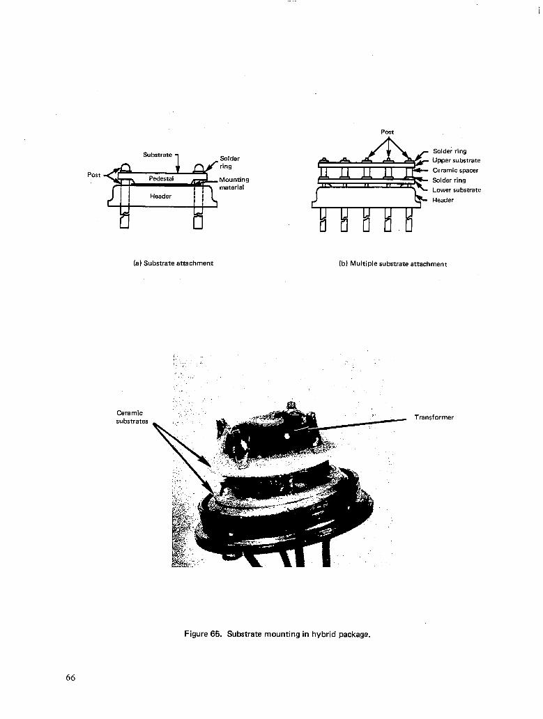
Post
Post
Solder ring
Mounting material
(a) Substrate attachment
Ceramic substrates
Solder ring Upper substrata
Ceramic spacer
Solder ring
Lower substrate
Header
(b) Multiple substrate attachment
Figure 65. Substrate mounting in hybrid package.
66
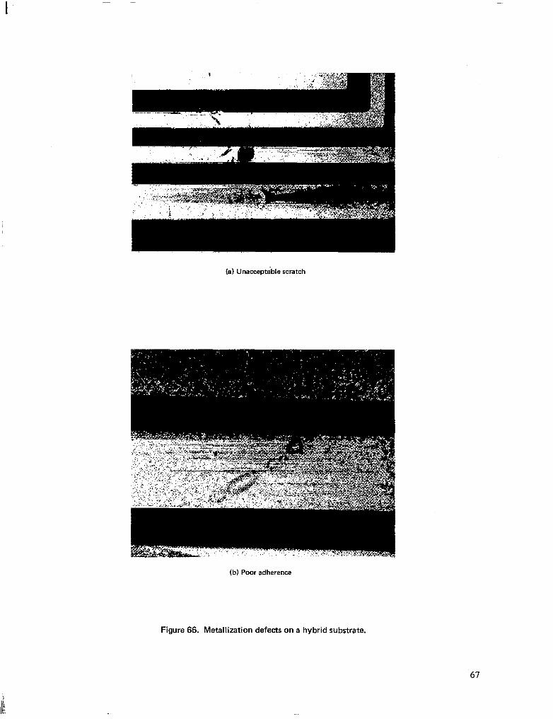
(a) Unacceptable scratch
(b) Poor adherence
Figure 66. Metallization defects on a hybrid substrate.
67
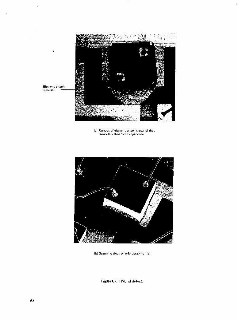
Element material
an ach
(a) Runout of element attach material that leaves less than I-mil separation
(b) Scanning electron micrograph of (a)
Figure 67. Hybrid defect.
68
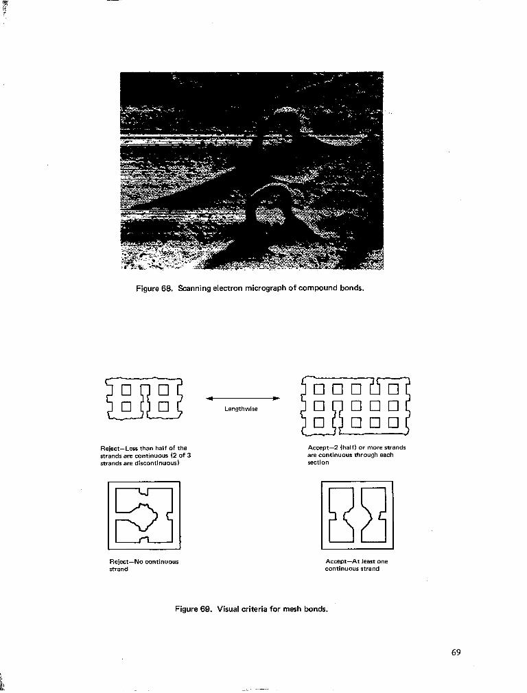
8;
Figure 68. Scanning electron micrograph of compound bonds.
* Lengthwise
Reject-Less than half of the strands are continuous (2 of 3 strands are discontinuous)
Accept-2 (half) or more strands are continuous through each section
I I
Reject-No continuous strand
Accept-At least one continuous strand
Figure 69. Visual criteria for mesh bonds.
69
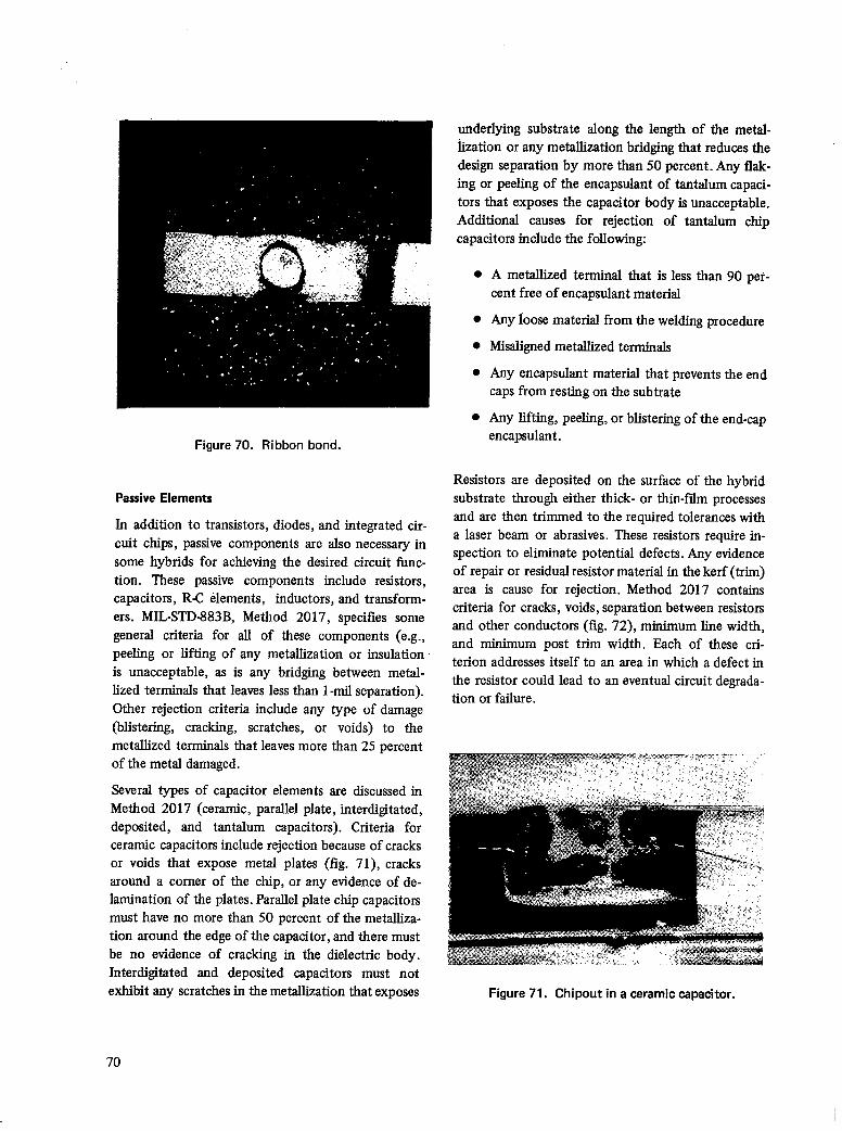
Figure 70. Ribbon bond.
underlying substrate along the length of the metal- hzation or any metalhzation bridging that reduces the design separation by more than 50 percent. Any flak- ing or peeling of the encapsulant of tantalum capaci- tors that exposes the capacitor body is unacceptable. Additional causes for rejection of tantalum chip capacitors include the following:
l A metallized terminal that is less than 90 per- cent free of encapsulant material
l Any loose material from the welding procedure
l Misaligned metallized terminals
0 Any encapsulant material that prevents the end caps from resting on the subtrate
l Any lifting, peeling, or blistering of the end-cap encapsulant.
Passive Elements Resistors are deposited on the surface of the hybrid substrate through either thick- or thin-film processes
In addition to transistors, diodes, and integrated cir- cult chips, passive components are also necessary in some hybrids for achieving the desired circuit func- tion. These passive components include resistors, capacitors, RC elements, inductors, and transform- ers. MIL-STD4383B, Method 2017, specifies some general criteria for all of these components (e.g., peeling or lifting of any metallization or insulation. is unacceptable, as is any bridging between metal- lized terminals that leaves less than I-mil separation). Other rejection criteria include any type of damage (blistering, cracking, scratches, or voids) to the metallized terminals that leaves more than 25 percent of the metal damaged.
Several types of capacitor elements are discussed in Method 2017 (ceramic, parallel plate, interdigitated, deposited, and tantalum capacitors). Criteria for ceramic capacitors include rejection because of cracks or voids that expose metal plates (fig. 71) cracks around a comer of the chip, or any evidence of de- lamination of the plates. Parallel plate chip capacitors must have no more than 50 percent of the metalliza- tion around the edge of the capacitor, and there must be no evidence of cracking in the dielectric body. Interdigltated and deposited capacitors must not exhibit any scratches in the metalhzation that exposes
and are then trimmed to the required tolerances with a laser beam or abrasives. These resistors require in- spection to eliminate potential defects. Any evidence of repair or residual resistor material in the kerf (trim) area is cause for rejection. Method 2017 contains criteria for cracks, voids, separation between resistors and other conductors (fig. 72) minimum line width, and minimum post trim width. Each of these cri- terion addresses itself to an area in which a defect in the resistor could lead to an eventual circuit degrada- tion or failure.
Figure 71. Chipout in a ceramic capacitor.
70
Ceramic substrate
Figure 72. Smear in a thin-film resistor that has been deposited on a ceramic substrate.
Package Conditions
The accept/reject criteria for foreign material (fig. 73) found in hybrids are similarly covered by the class S requirements of Method 2010 for monolithic inte- grated circuits, with the following additions. Method 2017 allows for verification of attached foreign ma- terial “by a light touch with an appropriate mechani- cal device ,” followed by a cleaning process. Method 2017 also specifies that the hybrid package seal sur- face must be free of physical damage or contamina- tion.
PRECAP SCENARIO
Many inspectors are trained in what to look for in a precap visual examination, but not how to proceed with one. The following paragraphs describe how a precap visual examination could proceed. The precap visual criteria vary among manufacturers and the quality level of the product. The criteria in this document basically follow those of MIL-STD-883B.
As mentioned previously, the final precap visual inspection should be carried out in a dust-free environ- ment (e.g., in a laminar flow hood). The low power examination is performed using a stereo zoom micro- scope capable of magnifications from 10X to 40X.
Smear
Thin-film resistor
The high power examination utilizes a microscope capable of magnifications from 40X to 400X. The lighting for this examination is through-the-lens vertical lighting. The low power examination uses oblique lighting.
Initially, the inspector views the devices at the lowest magnification. Manufacturers’ in-house specifications usually specify magnifications of 7X to 20X. MIL- STD-883B specifies a minimum of 30X for low mag- nification. It is good practice to briefly examine a device for foreign particles and the general quality of the wires before subjecting the device to a 20-psig nominal gas blow. The gas blow removes any loose foreign particles. However, if the pressure of the gas is improperly adjusted (too high) or the gas blow is Introduced too close to the device, it can disturb the wires. It is for this reason that the brief initial examination is performed-so that the inspector does not automatically attribute poor wire quality to the manufacturing process when the reason for the poor wire quality is mishandling.
After the brief inspection, the inspector can critically reexamine the device. A good place to begin is with the wires, looking at the takeoff angle of wires from the die, the positions of wires relative to one another,
71
and the overall general quality of the package interior. He can then proceed to looking for extraneous for- eign particles (including silicon particles), die position, gross die cracks, die attachment, and other defects easily visible at 10X to 40X. The inspector should view the device not only from the perpendicular, but also at angles 30 to 45’ from the perpendicular to detect difficult-to-see defects such as particles trap- ped between leads and the edge of the substrate.
After the low power examination, the inspector pro- ceeds to the high power examination. MIL-STD-883B requires high power examination to be performed at a minimum of 100X. Some specifications for precap visual criteria suggest a high magnification criteria based on die size as follows:
Die Size High-Magnification (minimum side dimension) Inspection (min .)
30 rnils or less 31 to 50 nils 51 to 1oomils Greater than 100 mils
200x 100x 50x 30x
These criteria may become practical, even necessary, in light of the new VLSI integrated circuits. A precap visual inspection at 200X on a VLSI chip is very time- consuming.
During the high power examination, the inspector views the semiconductor die for defects and performs a detailed inspection of peculiarities observed during the low power examination. The inspector reinspects bonding pads for misplaced wire bonds, overall metal- lization quality, scratches and voids, fine die cracks, mask alignment, and exposed silicon and/orjunctions. When viewing the die, he should follow a pattern to minimize the reinspection of die area already exam- ined. Figure 74 shows an example of such a pattern.
In addition to following the foregoing precap sce- nario, the inspector must be aware of:
l All potential problems introduced by the prior operations
l The manner in which these problems are visible, if at all
For&n material
Figure 73. Attached foreign material next to a bond- ing post. Note the unacceptable rework attachment of a wire by adhesive.
l The seriousness of these anomalies.
If the inspector is aware of these items and if the manufacturing company’s philosophy is to produce highly reliable devices, many potential problems can be screened out here. However, if the inspector is poorly trained or the company is not properly motivated, the tinal precap visual inspection is of little value. This is true for both integrated circuits and the more complex hybrid microcircuits.
Figure 74. Sample pattern for inspecting a die.
72

-
SUMMARY
This document concerns the final precap visual in- spection of microcircuit devices to detect manufac- turing defects and reduce failure rates in service. It outlines the processes employed in fabricating mono- lithic integrated circuits and hybrid microcircuits, discusses various failure mechanisms resulting from deficiencies in those processes, and gives the rudi- ments of performing final inspection. It does not dis- cuss the experience of the inspector or the optical equipment that is necessary for adequately perform- ing such inspections.
To adequately inspect high-reliability devices, an in- spector must be familiar with normal fabrication techniques and must be aware of the failure mech- anisms associated with these processes. In addition, the inspector must acquire considerable experience in using microscopes and must develop sufficient
tolerance to prevent eye fatigue while examining a relatively large number of devices.
The success of final precap visual inspection depends on both the motivation of the manufacturer and the training of the inspector. The lack of competently performed precap visual inspections of “high relia- bility” devices is evident by the number of defective “high reliability” devices reported by users. This docu- ment is intended to serve as a training guide for government and industry inspectors who perform pre- cap inspections.
ACKNOWLEDGMENT
The authors extend their appreciation to Phil Brussius of the Honeywell Corporation and Sam Longbrook of Micro Networks Company for material used in pre- paring portions of this report.
73
I lllllllll I I I I Illllll

REFERENCES
Harman, G. G. (1974), in Microelectronic Ultrasonic National Bureau of Standards (1972) Testing and Bonding, National Bureau of Standards, Special Fabrication of Wire-Bond Electrical Cormections- Publication 400-2;G. G., Harman, Ed. A Comprehensive Survey, Technical Note 726.
Harman, G. G., and Cannon, C. A. (1978). The Micro- electronic Wire Bond Test-How to Use It, How to Abuse It, IEEE Trans. on Components, Hybrids, Warner, R. M., Jr., Ed. (1965), Integrated Circuits: and Manufacturing Technology, CHMT-1, No. 3, Design Principles and Fabrication, McGraw-Hill pp. 203-210. Book Co., New York.
BIBLIOGRAPHY
Anstead, R. J. (1975) Techniques of Final Beseal Visual Inspection, NASA SP-65 09.
Doyle, E. A., Jr. (1981), How Parts Fail, IEEE Spectrum, No. 10, pp. 37-43.
Glaser, A. B., and Subak-Sharpe, G. E. (1979) Inte- grated Circuit Engineering, Addison-Wesley Pub- lishing Co., Reading, Mass.
Harman, G. G. (1974), Metallurgical Failure Modes of Wire Bonds, 12th Annual Proc. IEEE Reliability Physics Symposium,Las Vegas, Nevada, April 2-4, pp. 131-141.
Harman, G. G. (1979), Nondestructive Tests Used to Insure the Integrity of Semiconductor Devices, with Emphasis on Acoustic Emission Techniques, National Bureau of Standards, Special Publication 400-59.
Kleis, J., A Guide to Improved Bonding Wire, 1979, Sterndent Corp., New York, p. 11.
Ravi, D. V. (1981) Imperfections and Impurities in Semiconductor Silicon, John Wiley & Sons, New York.
Test Methods and Procedures for Microelectronics (1977),MIL-STD-883B, August 1977.
Van Nie, A. G., Goedbloed, W., and Kersuzan, G. (1981), Reliability and Degradation, in Reliability and Degradation of Mkrowave Integrated Circuits, M. J. Howes and D. V. Morgan, Eds., John Wiley & Sons, New York.
Williams, W. C. (1981), Lessons from NASA, IEEE Spectrum, No. 10, pp. 79-84.
Wood, J. (1981) Reliability and Degradation: Semi- conductor Devices and Circuits, in Reliability and Degradation of Silicon Devices and Integrated Cir- cuits, M. J. Howes and D. V. Morgan, Eds., John Wiley & Sons, New York.
75
1. Report No. -.
2. Government Accession No. --
3. Recipient’s Catalog No.
NASA RP-1122 4. Title and Subtitle 5. Report Date
November 1984 PROCEDURES FOR PRECAP VISUAL INSPECTION 6. P;prming Organization Code
~~~~ -~ -_.__i.- i --. - __ 7. Author(s) 8. Performing Organization Report No.
10. Work Unit No.
9. Performing Organization Name and Address National Aeronautics and Space Administration Office of the Chief Engineer 11. Contract or Grant No.
Systems Engineering and Technology Washington, D.C. 20546 13. Type of Report and Period Covered
12. Sponsoring Agency Name and Address Reference Publication
National Aeronautics and Space Administration 14. Sponsoring Agency Code
Washington, D.C. 20546
I5 Supplementary Notes
16. Abstract
This document describes screening procedures for the final precap visual inspection of microcircuits used in electronic system components. It is designed to aid in training personnel unfamiliar with microcircuits. The first part of this guide presents processing techniques used in industry for the manufacture of monolithic and hybrid components. Also discussed are imperfections that may be encountered during this inspection. Problem areas such as scratches, voids, adhesions, and wire bonding are illustrated by photomicrographs. This guide can serve as an effective tool in training personnel to perform precap visual inspections efficiently and reliably.
7. Key Words (Suggested by Author(s)) --. -----L---
18. Distribution Statement
microcircuits monolithic components hybrid components Unclassified-Unlimited
metallization Subject Category 33
9. Security Classif. (of this report1 20. Security Classif. (of this page) 21. No. of Pages 22. Price - - -
Unclassified Unclassified 75 A04
For sale by the National Technical information Service, Springfield, Virginia 22161 NASA-Langley, 1984