non-destructive contact resistivity measurements …...non-destructive contact resistivity...
TRANSCRIPT
Non-Destructive Contact Resistivity Measurements on Industrial Solar Cells
University of Central Florida (UCF): Kristopher O. Davis, Geoffrey Gregory
Foshan University, Gonda Electronic Technology: Zhihao Yang
BrightSpot Automation: Andrew Gabor, Andrew Anselmo, Rob Janoch
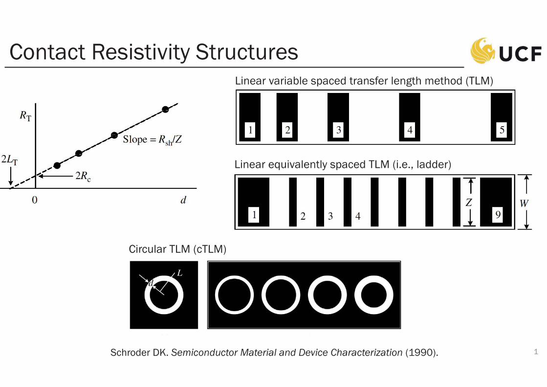
Contact Resistivity Structures
1Schroder DK. Semiconductor Material and Device Characterization (1990).
Linear variable spaced transfer length method (TLM)
Linear equivalently spaced TLM (i.e., ladder)
Circular TLM (cTLM)
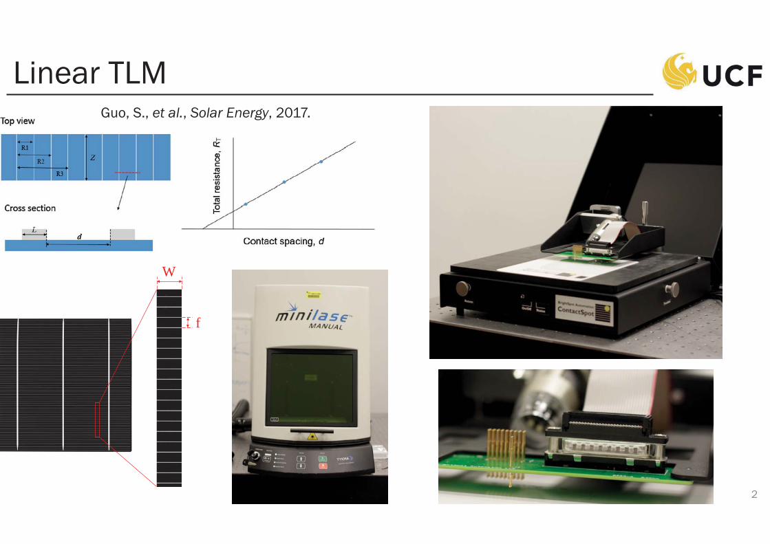
Linear TLM
2
W
f
Guo, S., et al., Solar Energy, 2017.
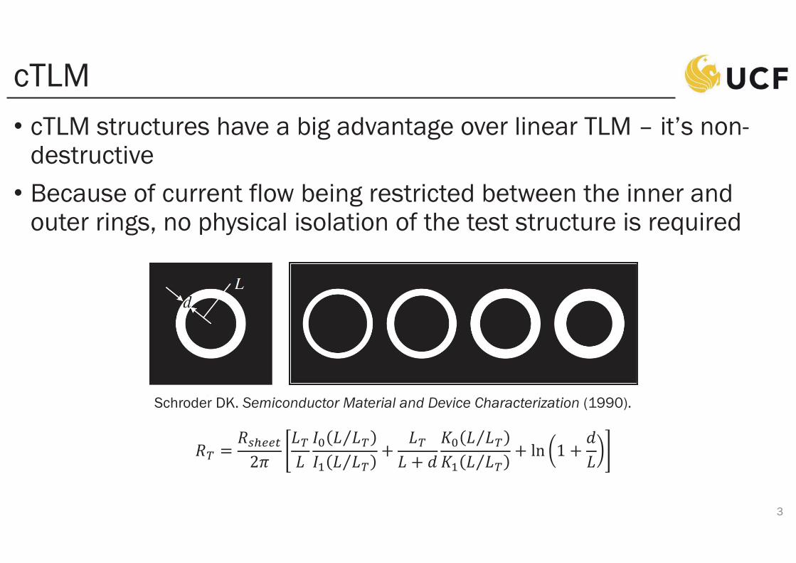
cTLMcTLM structures have a big advantage over linear TLM – it’s non-destructiveBecause of current flow being restricted between the inner and outer rings, no physical isolation of the test structure is required
3
Schroder DK. Semiconductor Material and Device Characterization (1990).
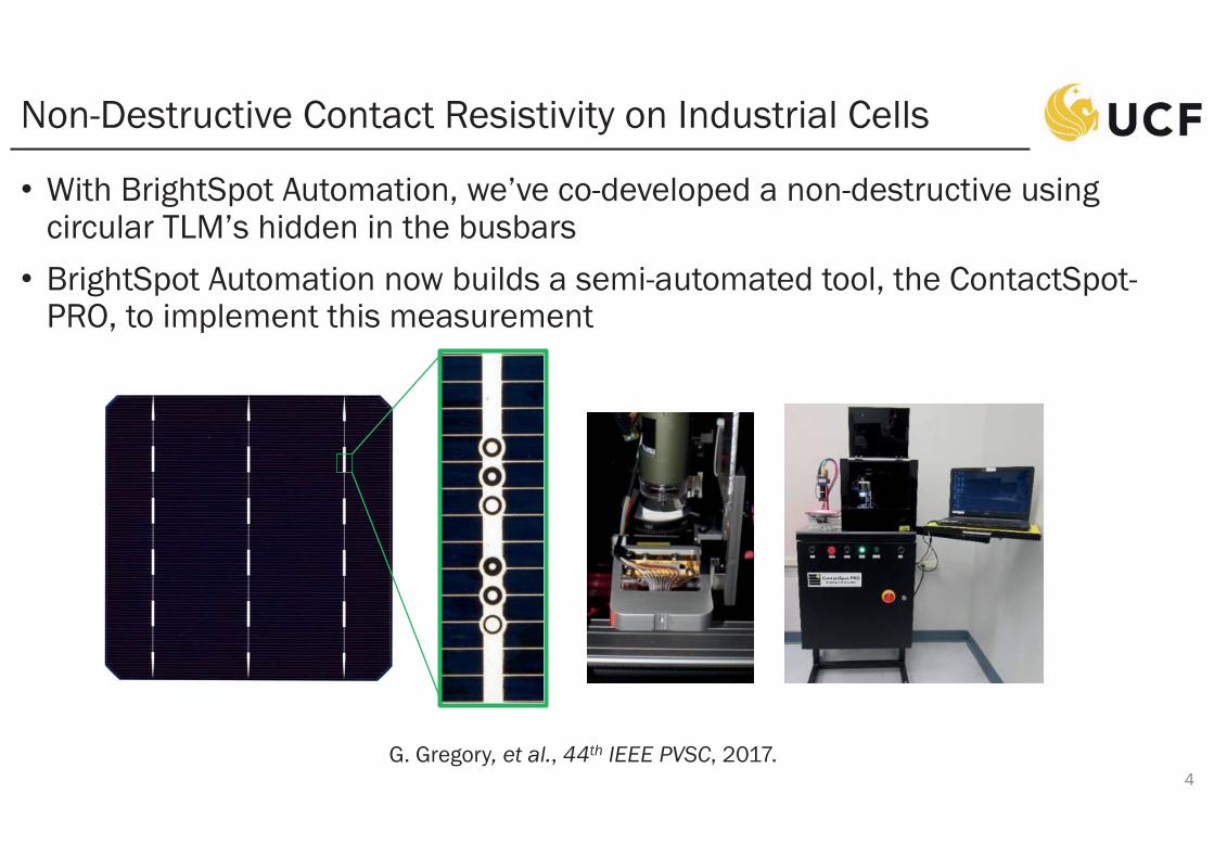
Non-Destructive Contact Resistivity on Industrial Cells
With BrightSpot Automation, we’ve co-developed a non-destructive using circular TLM’s hidden in the busbars
BrightSpot Automation now builds a semi-automated tool, the ContactSpot-PRO, to implement this measurement
4G. Gregory, et al., 44th IEEE PVSC, 2017.
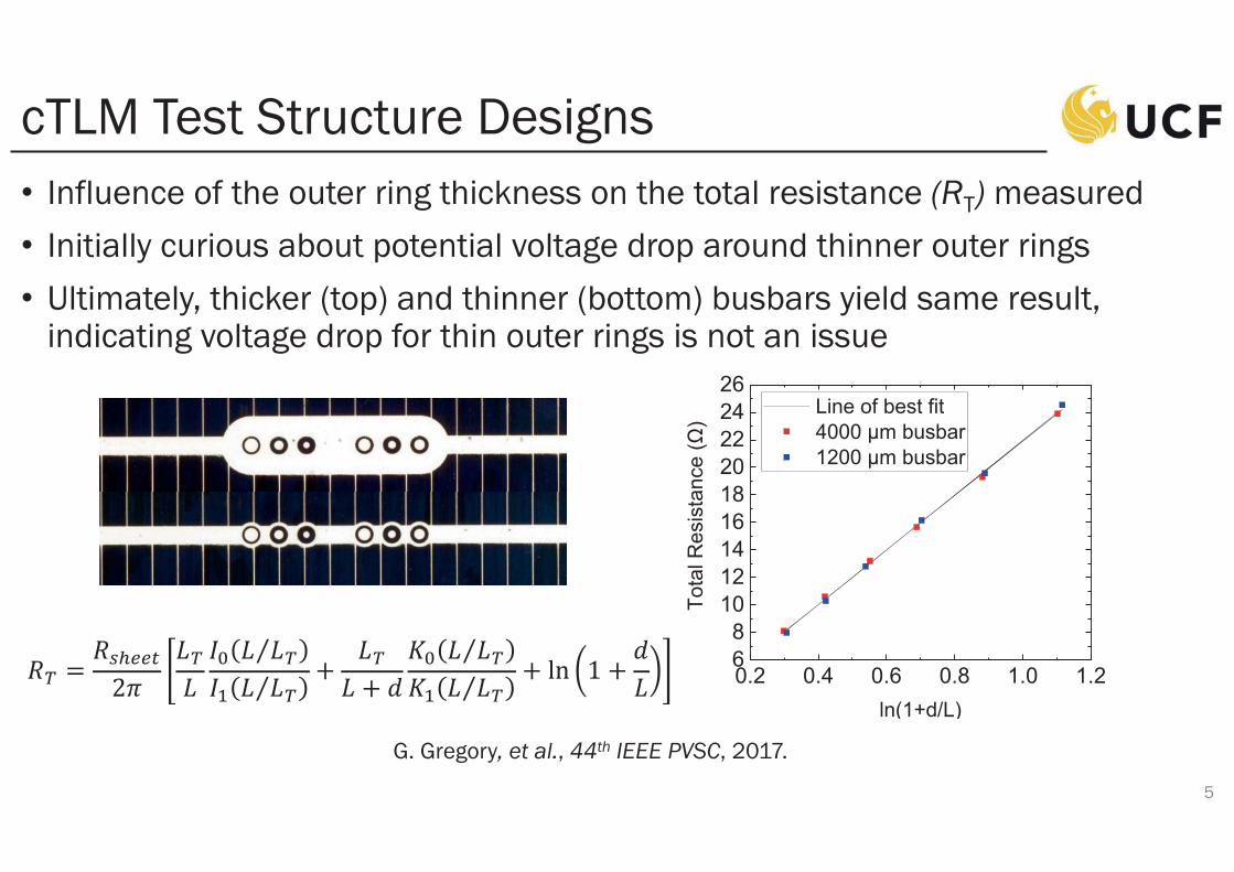
cTLM Test Structure DesignsInfluence of the outer ring thickness on the total resistance (RT) measured
Initially curious about potential voltage drop around thinner outer rings
Ultimately, thicker (top) and thinner (bottom) busbars yield same result, indicating voltage drop for thin outer rings is not an issue
5
G. Gregory, et al., 44th IEEE PVSC, 2017.
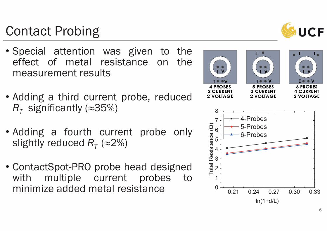
Contact ProbingSpecial attention was given to theeffect of metal resistance on themeasurement results
Adding a third current probe, reducedRT significantly (≈35%)
Adding a fourth current probe onlyslightly reduced RT (≈2%)
ContactSpot-PRO probe head designedwith multiple current probes tominimize added metal resistance
6
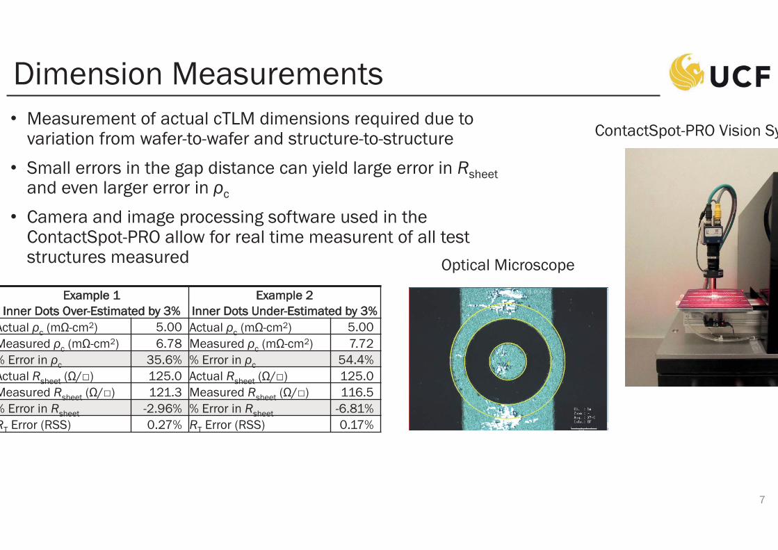
Dimension MeasurementsMeasurement of actual cTLM dimensions required due to variation from wafer-to-wafer and structure-to-structure
Small errors in the gap distance can yield large error in Rsheetand even larger error in ρc
Camera and image processing software used in the ContactSpot-PRO allow for real time measurent of all test structures measured
7
ContactSpot-PRO Vision Sy
Optical Microscope
Example 1Inner Dots Over-Estimated by 3%
Example 2Inner Dots Under-Estimated by 3%
Actual ρc (mΩ-cm2) 5.00 Actual ρc (mΩ-cm2) 5.00Measured ρc (mΩ-cm2) 6.78 Measured ρc (mΩ-cm2) 7.72% Error in ρc 35.6% % Error in ρc 54.4%Actual Rsheet (Ω/□) 125.0 Actual Rsheet (Ω/□) 125.0Measured Rsheet (Ω/□) 121.3 Measured Rsheet (Ω/□) 116.5% Error in Rsheet -2.96% % Error in Rsheet -6.81%RT Error (RSS) 0.27% RT Error (RSS) 0.17%
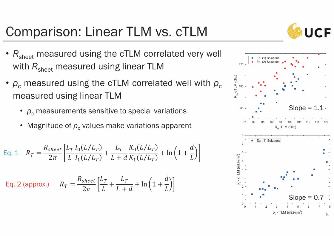
Comparison: Linear TLM vs. cTLMRsheet measured using the cTLM correlated very wellwith Rsheet measured using linear TLM
ρc measured using the cTLM correlated well with ρc
measured using linear TLM
ρc measurements sensitive to special variations
Magnitude of ρc values make variations apparent
8
Slope = 1.1
Slope = 0.7
Eq. 1
Eq. 2 (approx.)
Current and Future EffortsMore detailed uncertainty analysisMeasuring large data sets with comparisons and correlations between cTLM parameters and I-V + Suns-VOC parametersMore research into how this data can be used in manufacturing for R&D efforts, quality control, and process controlPerform measurements and investigate results for different contact materials, cell architectures, and contact interfaces
9
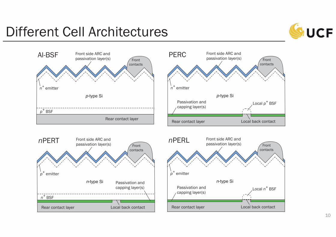
Different Cell Architectures
10
Rear contact layer
Front side ARC and passivation layer(s)
n+ emitter
Front contacts
Al-BSF
p-type Si
p+ BSF
Front side ARC and passivation layer(s)
n+ emitter
Front contacts
PERC
p-type SiPassivation and capping layer(s)
Rear contact layer Local back contact
Local p+ BSF
Front side ARC and passivation layer(s)
p+ emitter
Front contacts
nPERT
n-type Si Passivation and capping layer(s)
Rear contact layer Local back contact
Front side ARC and passivation layer(s)
p+ emitter
Front contacts
nPERL
n-type SiPassivation and capping layer(s)
Rear contact layer Local back contact
Local n+ BSF
n+ BSF
Different Cell Architectures
11
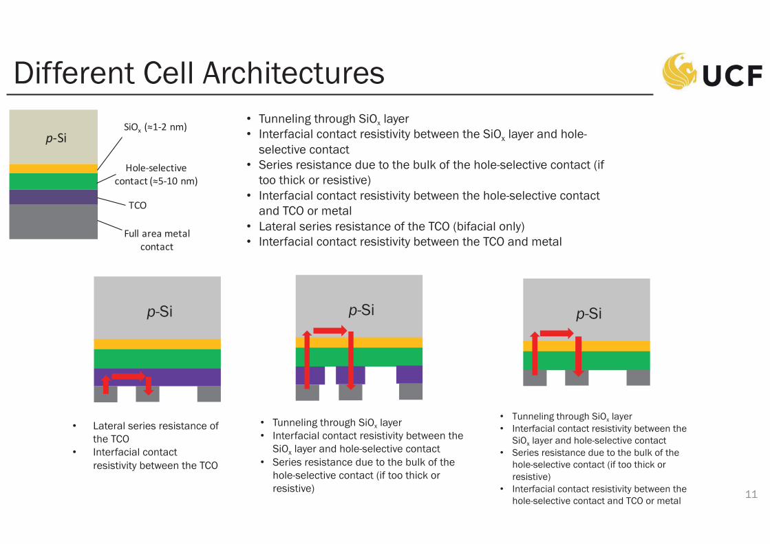
p-Si p-Si p-Si
Tunneling through SiOx layerInterfacial contact resistivity between the SiOx layer and hole-selective contactSeries resistance due to the bulk of the hole-selective contact (if too thick or resistive)Interfacial contact resistivity between the hole-selective contact and TCO or metalLateral series resistance of the TCO (bifacial only)Interfacial contact resistivity between the TCO and metal
Lateral series resistance of the TCOInterfacial contact resistivity between the TCO
Tunneling through SiOx layerInterfacial contact resistivity between the SiOx layer and hole-selective contactSeries resistance due to the bulk of the hole-selective contact (if too thick or resistive)
Tunneling through SiOx layerInterfacial contact resistivity between the SiOx layer and hole-selective contactSeries resistance due to the bulk of the hole-selective contact (if too thick or resistive)Interfacial contact resistivity between the hole-selective contact and TCO or metal
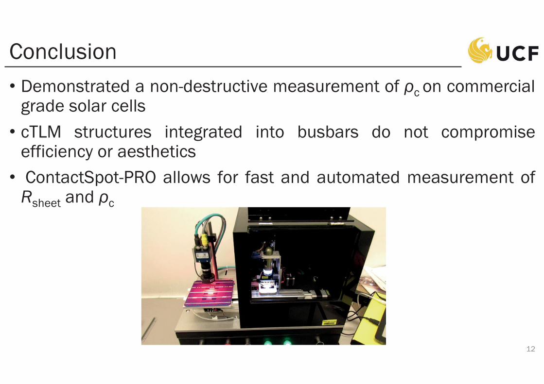
ConclusionDemonstrated a non-destructive measurement of ρc on commercialgrade solar cellscTLM structures integrated into busbars do not compromiseefficiency or aestheticsContactSpot-PRO allows for fast and automated measurement ofRsheet and ρc
12
Thanks!Team
University of Central FloridaBrightSpot AutomationFoshan UniversityGonda Electronic Technology
Corresponding Author:Kristopher [email protected]
Supported in part by the U. S Department of Energy SunShotInitiative under Award Number DE-EE0004947 and DE-EE0008155
13