noise characterization of analog to digital …jmfriedt.free.fr/rsi_adc_characterization.pdfnoise...
TRANSCRIPT
Noise Characterization of Analog to Digital Converters for Amplitude andPhase Noise Measurements
A.C. Cardenas-Olaya,1, 2, 3 E. Rubiola,3 J.-M., Friedt,3 P.-Y. Bourgeois,3 M. Ortolano,1, 2 S. Micalizio,1 and C.E.Calosso1
1)INRiM, Strada delle Cacce 91, 10135, Turin, Italy.2)Department of Electronic Engineering and Telecommunications, Politecnico di Torino, Corso Duca degli Abruzzi 24,10129, Turin, Italy.3)Department of Time and Frequency, FEMTO-ST, CNRS, Universite de Bourgogne Franche-Comte,26 chemin de l’Epitaphe, 25030, Besancon, France.
(Dated: 19 May 2017)
Improvements on electronic technology in recent years have allowed the application of digital techniquesin phase noise metrology where low noise and high accuracy are required, yielding flexibility in systemsimplementation and setup. This results in measurement systems with extended capabilities, additional func-tionalities and ease of use. In most digital schemes the Analog to Digital Converters (ADCs) set the ultimateperformance of the system, therefore the proper selection of this component is a critical issue. Currently,the information available in literature describes in depth the ADC features only at frequency offsets far fromthe carrier. However, the performance close to the carrier is a more important concern. As a consequence,the ADC noise is in general analyzed on the implemented phase measurement setup. We propose a noisemodel for ADCs and a method to estimate its parameters. The method retrieves the Phase Modulation andAmplitude Modulation noise by sampling around zero and maximum amplitude, a test sine-wave synchronouswith the ADC clock. The model allows discriminating the ADC noise sources and obtaining the phase noiseand amplitude noise power spectral densities from 10 Hz to one half of the sampling frequency. This ap-proach reduces data processing, allowing an efficient ADC evaluation in terms of hardware complexity andcomputational cost.
I. INTRODUCTION
New methods for the phase and amplitude noise mea-surement of oscillators have been proposed in the pastyears, based on digital systems1–8. Some reasons arejust obvious: reconfiguration flexibility and compact-ness of digital hardware. Others are more subtle.The traditional method based on two mixers and crossspectrum9–12 requires two oscillators at the same fre-quency of the oscillator under test, while in a fully digi-tal implementation arbitrary frequencies are synthesizednumerically with a resolution exceeding any practical use(∼6×10⁻¹⁸ with 64 bit numerically controlled oscillator).Another reason is that the traditional scheme suffers fromartifacts and errors13,14. Similar artifacts and errors, ifany, have still not been made clear in the case of digitalsystems.
The increasing technological advances on Analogto Digital Converters (ADCs), in terms of resolutionand sample rate, has allowed the implementation ofphase/amplitude noise metrology as ideal Software De-fined Radio (SDR) states15, sampling the signal of inter-est through a high-speed ADC and processing the datadigitally, reducing at minimum the analog components.However, the progress in digital measurement of ampli-tude and phase noise has been rather slow for a num-ber of reasons. First, the availability of converters withsufficient resolution and speed, i.e., converters with fea-tures such as 14 - 16 bits and sampling rates higher than100 Mega Samples per second (MSps), is rather recent.Second, the skill for digital hardware design and for Ra-
dio Frequency (RF) engineering, oscillators, spectral pu-rity, etc., are seldom found in the same team. Third,the measurement of amplitude and phase spectra rely onsome generally undocumented features of the converters.
This article focuses on a model of the ADC, specificfor the measurement of oscillators, and on a method toextract the parameters. We work on a Red Pitaya boardbecause this platform is suitable to our tests with an ac-ceptable experimental complexity. Resolution and speed(14 bit, 125 MSps) are reasonably close to the state ofthe art of ADCs (16 bit, 350 MSps or 14 bit, 1 GSps),and it is potentially sufficient for the implementation of acomplete instrument. Of course, similar test with cuttingedge converters will follow.
Different techniques have been developed for charac-terizing ADC. While the histogram approach has beenwidely used for measuring static errors16,17, one group18
proposed a method for estimating the voltage error gen-erated by the aperture jitter plus the internal additivenoise through the locked histogram technique, perform-ing synchronous sampling. The distribution function ofthe noise, assumed normal, was obtained by modifyingthe mean of the input sine-wave by adjusting an offset asfinely as one least significant bit (LSB) of the ADC undertest, being a suitable approach for ADCs of low/mediumresolution (maximum 10 bits). Other work19 proposeda model for the jitter of ADCs and a method based onSNR analysis in order to evaluate and discriminate theeffects of the jitter components on the ADC performance,thereby giving a guideline to compensate for such effectsin future high-speed ADC designs. A characterization
2
technique based on the use of a Graychip and down-conversion was performed1 for evaluating the viabilityand strategies of the direct-digital technique implemen-tation for phase noise measurements. Characterizationof high resolution, low speed ADCs (≥20 bit,≤5 MHz)have been performed20 using a Programmable Joseph-son Voltage Standard. Recent results of high-speed ADCnoise characterization were obtained through a full dig-ital approach based on common noise cancellation anddigital down-conversion21. The power spectra density ofADC phase noise is estimated after proper filtering anddecimation stages.
In view of the fast advances in technology for obtaininghigh speed and high resolution ADCs and in the frameof evaluating ADCs for phase/amplitude noise metrol-ogy applications, this work proposes a computationallow cost method for ADC noise characterization using acommercial system setup. We present a model for ADCnoise and measurement for determining their componentsthrough Phase Modulation (PM) and Amplitude Modu-lation (AM) analysis, tracking the relevant informationby synchronous sampling. The results of the charac-terization will provide information about the limit forphase/amplitude noise metrology allowing punctual con-sideration in measurement techniques design.
II. ADC NOISE MODEL
The model proposed in this work aims to discriminatethe different noise contributions of an analog to digitalconversion in the basis of two random noise classes: ad-ditive and parametric22. Additive noise refers to a noiseprocess that can be represented as a voltage or a currentadded to the signal, caused by the thermal noise on re-sistive elements and by shot and avalanche noise presentin the junctions of semiconductors23. This noise is gen-erated in the signal bandwidth and it is always present,even without carrier information. Instead, parametricnoise refers to a non-linear near-DC process caused bynon linearities present in electronic circuits due to con-tamination in semiconductors materials23. It is trans-lated by action of a carrier, generating amplitude and/orphase modulation on the signal.
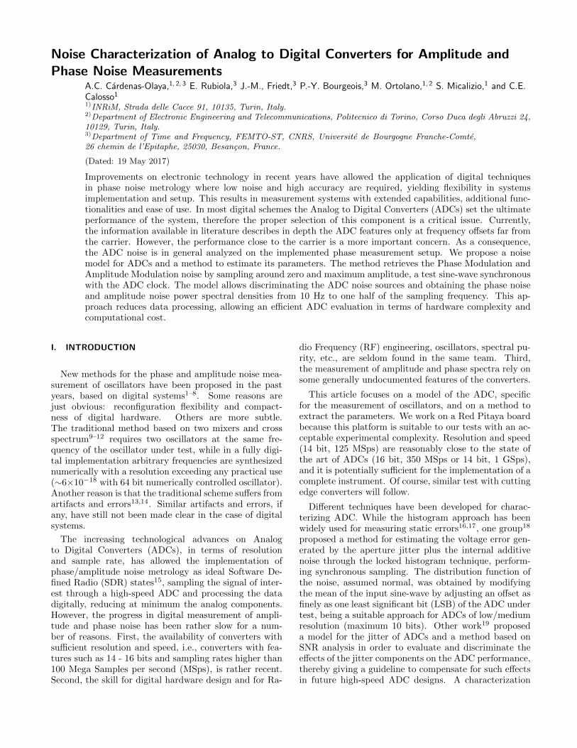
Our ADC noise modeling focuses on four main noisesources, as it is depicted in FIG. 1(a): input stage, aper-ture jitter, voltage reference and quantization.
The contribution of the noise generated by the inputstage has two components: additive and parametric. Forthe model proposed here, this noise source is assumedto be dominated by the additive noise n(t). This as-sumption is verified through the experimental results re-ported in section IV. Hence, considering an input signalv(t), the effect of the input stage noise is expressed asv ′(t) = v(t) + n(t).
The aperture jitter, x(t), defined as the variation ofthe sampling instant kTs, is caused by time fluctuationsin the sample and hold24,25. These time fluctuations
(a) ADC noise model.
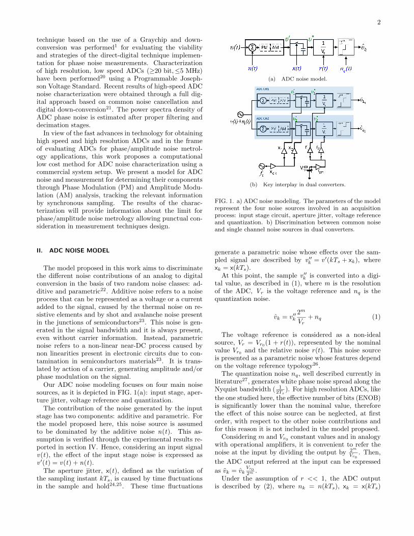
(b) Key interplay in dual converters.
FIG. 1. a) ADC noise modeling. The parameters of the modelrepresent the four noise sources involved in an acquisitionprocess: input stage circuit, aperture jitter, voltage referenceand quantization. b) Discrimination between common noiseand single channel noise sources in dual converters.
generate a parametric noise whose effects over the sam-pled signal are described by v ′′k = v ′(kTs + xk ), wherexk = x(kTs).
At this point, the sample v ′′k is converted into a digi-tal value, as described in (1), where m is the resolutionof the ADC, Vr is the voltage reference and nq is thequantization noise.
vk = v′′k2m
Vr+ nq (1)
The voltage reference is considered as a non-idealsource, Vr = Vr0(1 + r(t)), represented by the nominalvalue Vr0 and the relative noise r(t). This noise sourceis presented as a parametric noise whose features dependon the voltage reference typology26.
The quantization noise nq, well described currently inliterature27, generates white phase noise spread along theNyquist bandwidth ( 1
2Ts). For high resolution ADCs, like
the one studied here, the effective number of bits (ENOB)is significantly lower than the nominal value, thereforethe effect of this noise source can be neglected, at firstorder, with respect to the other noise contributions andfor this reason it is not included in the model proposed.
Considering m and Vr0 constant values and in analogywith operational amplifiers, it is convenient to refer thenoise at the input by dividing the output by 2m
Vr0. Then,
the ADC output referred at the input can be expressed
as vk = vkVr02m .
Under the assumption of r << 1, the ADC outputis described by (2), where nk = n(kTs), xk = x(kTs)
3
and rk = r(kTs) are discrete-time random processes ob-tained from sampling the corresponding continuous-timerandom process at t = kTs.
vk = (nk + v(kTs + xk))(1− rk) (2)
Now that the ADC output is stated in terms of thenoise sources we can analyze their effects using a properinput for discriminating their contributions. Follow-ing (2), the contribution of xk propagates to the ADCoutput depending on the slew rate of the input signal,while the impact of rk depends on the input signal level.Note that in the case of v(t) = 0, the contribution ofthe aperture jitter and the voltage reference noise arenegligible, therefore the ADC output corresponds to theadditive noise of the input stage.
Then, assuming v(t) = V0cos(2πν0t) as input signal ofthe ADC, case of interest for time and frequency appli-cations, we can rewrite (2) as
vk = (nk + V0 cos(2πν0(kTs + xk)))(1− rk) (3)
Considering nk, xk and rk independent processes, thetotal amplitude and phase noise generated by the ADCcan be expressed as the sum of the different amplitudeand phase fluctuations induced by each noise source, re-spectively. The additive noise of the input stage nkgenerates amplitude and phase noise on the signal con-verted. In order to better discriminate its effects, thisnoise source is decomposed in its in-phase and quadra-ture components, nα and nϕ respectively. Under lownoise conditions22, |nα/V0| 1 and |nϕ/V0| 1, thenormalized amplitude noise generated by nk is expressedas αnα = (1/V0)nα while the induced phase noise is givenby ϕnϕ = (1/V0)nϕ.
The aperture jitter xk results in pure phase modulationon the analog to digital conversion given by ϕx = 2πν0x.The maximum voltage variations induced by this noisesource occur at the samples of highest slew rate (SR), i.e.,close to the zero-crossings and are described by V02πν0xk.Moreover, it is worth to remark that the samples of max-imum amplitude are not influenced by this noise con-tribution at the first order. Instead, they are directlyrelated to the voltage reference noise presented as ampli-tude modulation on the signal converted. It generates amaximum voltage error V0rk that occurs at the maximumamplitude samples of the input signal.
Hence, the total ADC phase noise ϕk and the totalADC amplitude noise αk are described in (4), where ϕkis in radians and αk is non-dimensional, being the nor-malized amplitude fluctuations22.
ϕk = ϕnϕk + ϕxk =1
V0nϕk + 2πν0xk (4)
αk = αnαk + rk =1
V0nαk + rk
Since power spectral density (PSD) and polynomiallaw are considered meaningful tools for noise description
and analysis due to the straightforward identification ofthe different noise processes22, they are used for repre-senting the ADC noise contributions. Hence, the PSDof the ADC phase noise in rad2/Hz and the PSD of theADC amplitude noise in 1/Hz are described in (5), wherethe integer N < 0 depends on the device.
Sϕ,s(f) =
0∑j=N
bsjfj Sα,s(f) =
0∑j=N
hsjfj (5)
The difference between the analog bandwidth B andthe sampling frequency fs in a digital circuit gener-ates aliasing on the white noise region of the sam-pled signal spectrum28. Hence, the voltage noise spec-trum of the sampled signal can be represented as
Sv(f) = 2Bfs
h0 +−1∑j=N
hjfj [V2/Hz]. For the case of
the aperture jitter, aliasing is generated in the whitenoise region of the spectrum, caused by the fact thatthese fluctuations are sampled at the sampling clock(fs). Thus, the spectrum of xk can be expressed as
Sx,s(f) = 2fs
J2 +−1∑j=N
kjfj [s2/Hz], where J is the root
mean square (rms) time fluctuation of the aperture jitterand k0 = 2
fsJ2. The spectrums of nϕk , nαk [V2/Hz] and
rk [1/Hz] represented through the polynomial law are de-scribed in (6). Since rk represents a relative amplitudenoise, the coefficients hrj are non-dimensional.
Snϕ,s(f) =
0∑j=N
hϕjfj [V2/Hz] (6)
Snα,s(f) =
0∑j=N
hαjfj [V2/Hz]
Sr,s(f) =
0∑j=N
hrjfj [1/Hz]
Hence, from (4), the spectrums of the phase and am-plitude noise of the ADC are
Sϕ,s(f) =1
V 20
Snϕ,s(f) + 4π2ν02Sx,s(f) (7)
Sα,s(f) =1
V 20
Snα,s(f) + Sr,s(f)
In this manner, from (7) the contribution of each noisesource for each different noise process could be identifiedhaving a complete description of the device limitations.
III. METHOD FOR ADC NOISE CHARACTERIZATION
As second part of this work, we propose a method fordetermining the ADC noise components stated in themodel. The method is based on data acquisitions under
4
three different measurement conditions that allow char-acterizing the three main noise process of the model: in-put stage, aperture jitter and voltage reference. In thefirst condition, the input of the ADC is connected toground through a 50 Ω resistor. In this case, the contri-bution of x(t) and r(t) are negligible, since the slew rateand the level of the signal are zero. Therefore, the volt-age noise on the data acquired is totally related to theadditive noise of input stage. The other two measure-ments are made by sampling synchronously two pointsof the cosine-wave at the input: the zero-crossings andthe peak values.
Considering that the voltage noise of the zero-crossingsis directly related to phase fluctuations (PM), the mea-surement of these variations will result in the estimationof the phase noise generated by nϕ(t) and x(t). On theother hand, the voltage noise on the peak values is repre-sentative of the amplitude fluctuations (AM), thereforethe measurement of the variation of these samples fromperiod to period will yield the amplitude noise added bynα(t) and r(t). Hence, the total ADC noise can be esti-mated through these measures as described in (8), whereSv,ϕ and Sv,α are the PSD of the voltage noise of thesignal sampled at zero-crossings and at the peak values,respectively.
Sϕ,s(f) =1
V 20
Sv,ϕ (8)
Sα,s(f) =1
V 20
Sv,α
It is important to notice that with a single channelconfiguration, the noise obtained is also influenced by thenoise contributions of the sampling clock and the inputsignal generator. Since the objective of this work is tocharacterize the ADC for phase noise metrology which,in general, is based on differential techniques, we pro-pose a configuration with two independent channels asdepicted in FIG. 1(b). The common noise contributionssuch as the one coming from the input signal generator,the sampling clock and the voltage reference are canceledby subtracting the data obtained from the two channels.In consequence, the noise estimated is the contribution ofthe two ADC channels. Since the channels are assumedto be uncorrelated, the noise of a single channel is halfthe total noise.
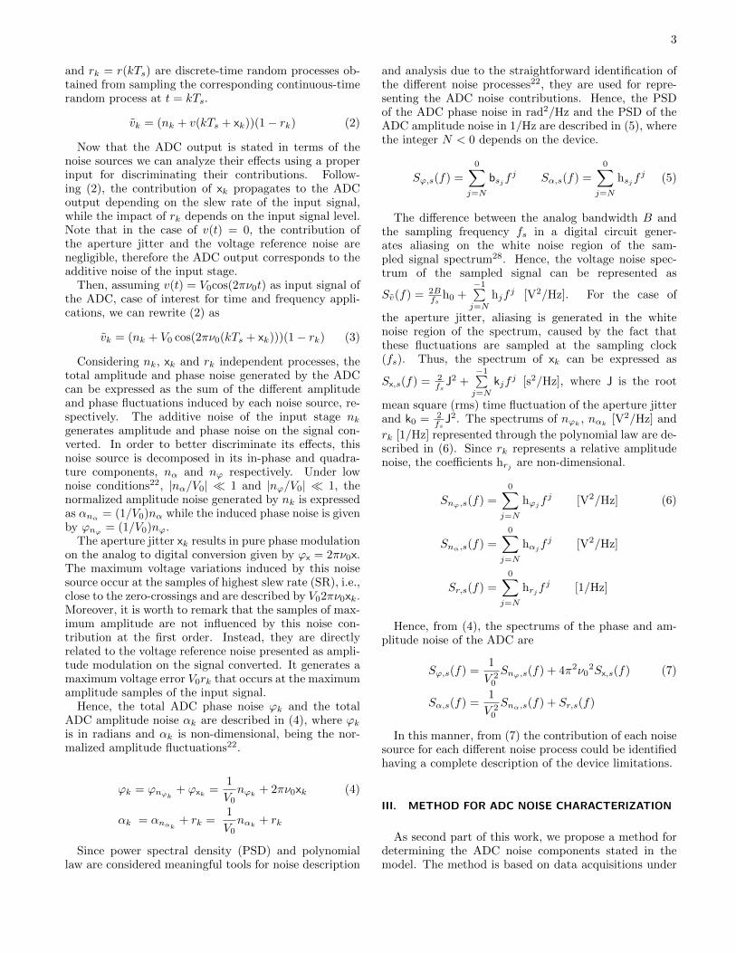
The scheme of the synchronous sampling system, thatis in charge of acquiring the zeros-crossings and the peaksof the cosine-wave, is shown in FIG. 2. The principleof operation consists in aligning the input signal to thesampling clock by means of a Phase Locked Loop (PLL):the input signal is sampled and sent to a Proportional-Integral controller (PI) which drives the frequency of thesignal generator through a DAC, providing the properphase information. The input signal generator works asa Voltage Controlled Oscillator (VCO) correcting the sig-nal generated to acquire the selected point, either for AMor PM characterization. When the loop is closed and thecontroller forces the acquisition of the zero-crossings (PM
FIG. 2. The scheme proposed allows sampling synchronouslyone sample per period in order to measure, through its varia-tions, the ADC noise effect on the output, as amplitude andphase fluctuations. The implementation is based on a dualADC and through the difference of the two outputs the com-mon noise is canceled obtaining only the corresponding noisecontribution of each channel.
characterization), it is possible to sample input signalsmultiple of the sampling clock by means of sub-sampling.To extend the measurements at lower frequencies (ν0 sub-multiple of fclk) the data rate is down-sampled. There-fore, the sampling frequency fs becomes equal to theinput frequency ν0, (fs = fclk
M = ν0). For AM char-acterization, we provide an input frequency not higherthan quarter the sampling clock in order to guaranteethe peaks acquisition. In this case, the system is still syn-chronized through the zero-crossings but only the peakvalues are acquired.
The PSD of the ADC noise is estimated in a bandwidthequal to the Nyquist frequency. The corresponding infor-mation at low frequencies is obtained through six stagesof decimation in order to acquire data down to 10 Hzor less according to the sampling frequency. Blocks of16384 data per channel are post-processed offline usingMATLAB.
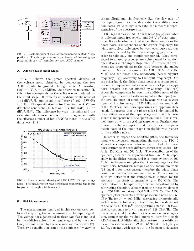
FIG. 3 depicts a simplified block diagram of themethod implemented in the Red Pitaya platform29. Thelater is an open source embedded system, that includesa dual-channel 14 bit ADC at 125 MSps LTC2145 fromLinear Technology, a dual-channel 14 bit DAC at 125MSps DAC1401D125 from NXP Semiconductors and aZynq 7010 System On Chip (SoC) from Xilinx. The in-put stage of Red Pitaya was modified by bypassing theamplifier and the low pass filter with a 1:1 RF trans-former, allowing the acquisition of sine-wave signals upto 500 MHz in order to increase the input bandwidth andto expose the jitter effect. In this regard, the samplingand hold has a bandwidth of 750 MHz.
IV. RESULTS
All the results presented in common mode are alreadyscaled by -3 dB in order to analyze the noise of one ADCchannel.
5
FIG. 3. Block diagram of method implemented in Red Pitayaplatform. The data processing is performed offline using ap-proximately 2× 10⁹ samples per each ADC channel.
A. Additive Noise Input Stage
FIG. 4 shows the power spectral density ofthe voltage noise obtained by connecting the twoADC inputs to ground through a 50 Ω resistor,(v(t) = 0 V, fs = 125 MHz). As described in section II,this noise corresponds to the voltage error induced bythe input stage. It presents an additive white noise of-154 dBV2/Hz and an additive flicker of -107 dBV2/Hzat 1 Hz. The quantization noise floor for the ADC un-der these conditions (14 bits and 2 V full scale) is -167dBV2/Hz27. The difference between this value and theestimated white noise floor is 13 dB, in agreement withthe effective number of bits (ENOB) stated in the ADCdatasheet (11.8).
FIG. 4. Power spectral density of ADC LTC2145 input stagenoise. The measurement was performed connecting the inputto ground through a 50 Ω resistor.
B. PM Measurements
The measurements analyzed in this section were per-formed acquiring the zero-crossings of the input signal.The voltage noise generated in these samples is inducedby the additive noise of the input stage and by the aper-ture jitter multiplied by the slew rate, as described in (7).These two contributions can be discriminated by varying
the amplitude and the frequency (i.e. the slew rate) ofthe input signal: for low slew rate, the additive noisedominates, while at high slew rate, the measure is repre-sentative of the aperture jitter.
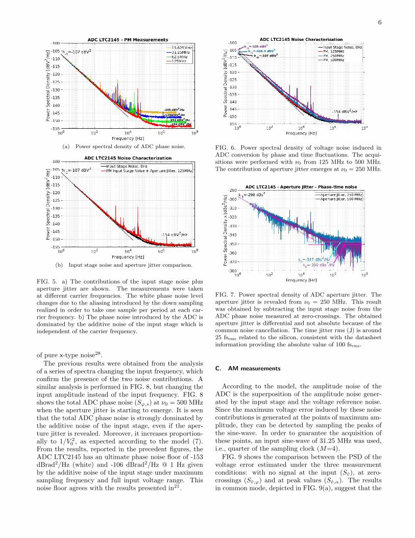
FIG. 5(a) shows the ADC phase noise (Sv,ϕ) estimatedat different input frequencies and 0.9 V of peak ampli-tude. It can be observed that under these conditions thephase noise is independent of the carrier frequency; thewhite noise floor differences between each curve are dueto aliasing caused by the down sampling performed inorder to take only one sample per period. They corre-spond to aliased ϕ-type, phase noise caused by randomfluctuations in the input stage circuit28, where the vari-ations are proportional to the ratio between the analogbandwidth B (for the case of the ADC LTC2145 is 750MHz) and the phase noise bandwidth (actual Nyquist
frequency, fclk2M , according to the input frequency). On
the other hand, the flicker phase noise is constant for allthe input frequencies being the signature of pure ϕ-typenoise, because it is not affected by aliasing. FIG. 5(b)shows the comparison between the additive noise of theinput stage (measured with no signal at the input) andthe zero-crossings noise induced by acquiring a sine-waveinput with a frequency of 125 MHz and an amplitudeof 0.9 V. These two noise spectrums are approximatelyequal. It suggests that the phase noise is dominated bythe additive noise of the input stage and that this noisesource is independent of the operation point. This is ver-ified later on with the AM measurements. Furthermore,it confirms the assumption that, in this case, the para-metric noise of the input stage is negligible with respectto the additive noise.
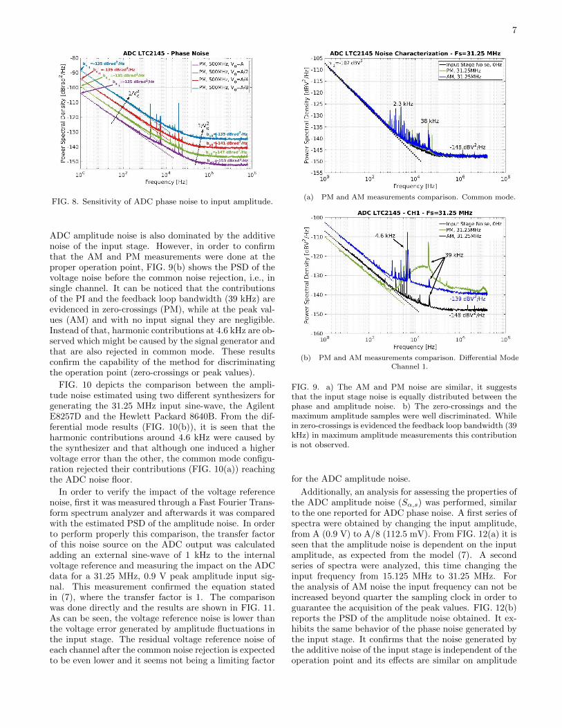
In order to expose the aperture jitter, the frequencyinput was increased, augmenting the slew rate. FIG. 6shows the comparison between the PSD of the phasenoise estimated at three different carrier frequencies: 125MHz, 250 MHz and 500 MHz. The contribution of theaperture jitter can be appreciated from 250 MHz, espe-cially in the flicker region, and it is more evident at 500MHz. For frequencies higher than the sampling clock, thephase noise bandwidth remains at the maximum value(M equal 1 for these cases), therefore the white phasenoise floor reaches the minimum value. From these re-sults we notice that the voltage noise induced by theaperture jitter starts to emerge at ν0 = 250 MHz. Thecontribution of the aperture jitter can be estimated bysubtracting the additive noise from the measures done atν0 = 250 MHz and at ν0 = 500 MHz (FIG. 7). The ADCaperture jitter presents a white phase-time noise of -350dBs2/Hz for ν0 = 500 MHz, decreasing proportionallywith the input frequency. According to the datasheetof the ADC LTC214530, the aperture jitter is 100 fsrms,that corresponds to a white noise of -338 dBs2/Hz. Thediscrepancy could be due to the common noise rejec-tion, estimating the residual aperture jitter for a singleADC channel. Additionally, the aperture jitter exhibits aflicker phase-time noise of -298 dBs2/Hz at 1 Hz (
√k−1 =
1.3 fs), constant with respect to the frequency, signature
6
(a) Power spectral density of ADC phase noise.
(b) Input stage noise and aperture jitter comparison.
FIG. 5. a) The contributions of the input stage noise plusaperture jitter are shown. The measurements were takenat different carrier frequencies. The white phase noise levelchanges due to the aliasing introduced by the down samplingrealized in order to take one sample per period at each car-rier frequency. b) The phase noise introduced by the ADC isdominated by the additive noise of the input stage which isindependent of the carrier frequency.
of pure x-type noise28.The previous results were obtained from the analysis
of a series of spectra changing the input frequency, whichconfirm the presence of the two noise contributions. Asimilar analysis is performed in FIG. 8, but changing theinput amplitude instead of the input frequency. FIG. 8shows the total ADC phase noise (Sϕ,s) at ν0 = 500 MHzwhen the aperture jitter is starting to emerge. It is seenthat the total ADC phase noise is strongly dominated bythe additive noise of the input stage, even if the aper-ture jitter is revealed. Moreover, it increases proportion-ally to 1/V 2
0 , as expected according to the model (7).From the results, reported in the precedent figures, theADC LTC2145 has an ultimate phase noise floor of -153dBrad2/Hz (white) and -106 dBrad2/Hz @ 1 Hz givenby the additive noise of the input stage under maximumsampling frequency and full input voltage range. Thisnoise floor agrees with the results presented in21.
FIG. 6. Power spectral density of voltage noise induced inADC conversion by phase and time fluctuations. The acqui-sitions were performed with ν0 from 125 MHz to 500 MHz.The contribution of aperture jitter emerges at ν0 = 250 MHz.
FIG. 7. Power spectral density of ADC aperture jitter. Theaperture jitter is revealed from ν0 = 250 MHz. This resultwas obtained by subtracting the input stage noise from theADC phase noise measured at zero-crossings. The obtainedaperture jitter is differential and not absolute because of thecommon noise cancellation. The time jitter rms (J) is around25 fsrms related to the silicon, consistent with the datasheetinformation providing the absolute value of 100 fsrms.
C. AM measurements
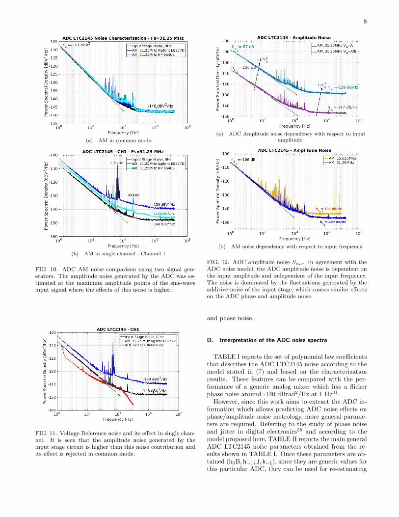
According to the model, the amplitude noise of theADC is the superposition of the amplitude noise gener-ated by the input stage and the voltage reference noise.Since the maximum voltage error induced by these noisecontributions is generated at the points of maximum am-plitude, they can be detected by sampling the peaks ofthe sine-wave. In order to guarantee the acquisition ofthese points, an input sine-wave of 31.25 MHz was used,i.e., quarter of the sampling clock (M=4).
FIG. 9 shows the comparison between the PSD of thevoltage error estimated under the three measurementconditions: with no signal at the input (Sv), at zero-crossings (Sv,ϕ) and at peak values (Sv,α). The resultsin common mode, depicted in FIG. 9(a), suggest that the
7
FIG. 8. Sensitivity of ADC phase noise to input amplitude.
ADC amplitude noise is also dominated by the additivenoise of the input stage. However, in order to confirmthat the AM and PM measurements were done at theproper operation point, FIG. 9(b) shows the PSD of thevoltage noise before the common noise rejection, i.e., insingle channel. It can be noticed that the contributionsof the PI and the feedback loop bandwidth (39 kHz) areevidenced in zero-crossings (PM), while at the peak val-ues (AM) and with no input signal they are negligible.Instead of that, harmonic contributions at 4.6 kHz are ob-served which might be caused by the signal generator andthat are also rejected in common mode. These resultsconfirm the capability of the method for discriminatingthe operation point (zero-crossings or peak values).
FIG. 10 depicts the comparison between the ampli-tude noise estimated using two different synthesizers forgenerating the 31.25 MHz input sine-wave, the AgilentE8257D and the Hewlett Packard 8640B. From the dif-ferential mode results (FIG. 10(b)), it is seen that theharmonic contributions around 4.6 kHz were caused bythe synthesizer and that although one induced a highervoltage error than the other, the common mode configu-ration rejected their contributions (FIG. 10(a)) reachingthe ADC noise floor.
In order to verify the impact of the voltage referencenoise, first it was measured through a Fast Fourier Trans-form spectrum analyzer and afterwards it was comparedwith the estimated PSD of the amplitude noise. In orderto perform properly this comparison, the transfer factorof this noise source on the ADC output was calculatedadding an external sine-wave of 1 kHz to the internalvoltage reference and measuring the impact on the ADCdata for a 31.25 MHz, 0.9 V peak amplitude input sig-nal. This measurement confirmed the equation statedin (7), where the transfer factor is 1. The comparisonwas done directly and the results are shown in FIG. 11.As can be seen, the voltage reference noise is lower thanthe voltage error generated by amplitude fluctuations inthe input stage. The residual voltage reference noise ofeach channel after the common noise rejection is expectedto be even lower and it seems not being a limiting factor
(a) PM and AM measurements comparison. Common mode.
(b) PM and AM measurements comparison. Differential ModeChannel 1.
FIG. 9. a) The AM and PM noise are similar, it suggeststhat the input stage noise is equally distributed between thephase and amplitude noise. b) The zero-crossings and themaximum amplitude samples were well discriminated. Whilein zero-crossings is evidenced the feedback loop bandwidth (39kHz) in maximum amplitude measurements this contributionis not observed.
for the ADC amplitude noise.
Additionally, an analysis for assessing the properties ofthe ADC amplitude noise (Sα,s) was performed, similarto the one reported for ADC phase noise. A first series ofspectra were obtained by changing the input amplitude,from A (0.9 V) to A/8 (112.5 mV). From FIG. 12(a) it isseen that the amplitude noise is dependent on the inputamplitude, as expected from the model (7). A secondseries of spectra were analyzed, this time changing theinput frequency from 15.125 MHz to 31.25 MHz. Forthe analysis of AM noise the input frequency can not beincreased beyond quarter the sampling clock in order toguarantee the acquisition of the peak values. FIG. 12(b)reports the PSD of the amplitude noise obtained. It ex-hibits the same behavior of the phase noise generated bythe input stage. It confirms that the noise generated bythe additive noise of the input stage is independent of theoperation point and its effects are similar on amplitude
8
(a) AM in common mode.
(b) AM in single channel - Channel 1.
FIG. 10. ADC AM noise comparison using two signal gen-erators. The amplitude noise generated by the ADC was es-timated at the maximum amplitude points of the sine-waveinput signal where the effects of this noise is higher.
FIG. 11. Voltage Reference noise and its effect in single chan-nel. It is seen that the amplitude noise generated by theinput stage circuit is higher than this noise contribution andits effect is rejected in common mode.
(a) ADC Amplitude noise dependency with respect to inputamplitude.
(b) AM noise dependency with respect to input frequency.
FIG. 12. ADC amplitude noise Sα,s. In agreement with theADC noise model, the ADC amplitude noise is dependent onthe input amplitude and independent of the input frequency.The noise is dominated by the fluctuations generated by theadditive noise of the input stage, which causes similar effectson the ADC phase and amplitude noise.
and phase noise.
D. Interpretation of the ADC noise spectra
TABLE I reports the set of polynomial law coefficientsthat describes the ADC LTC2145 noise according to themodel stated in (7) and based on the characterizationresults. These features can be compared with the per-formance of a generic analog mixer which has a flickerphase noise around -140 dBrad2/Hz at 1 Hz31.
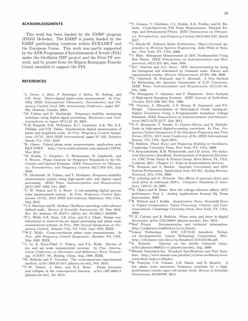
However, since this work aims to extract the ADC in-formation which allows predicting ADC noise effects onphase/amplitude noise metrology, more general parame-ters are required. Referring to the study of phase noiseand jitter in digital electronics28 and according to themodel proposed here, TABLE II reports the main generalADC LTC2145 noise parameters obtained from the re-sults shown in TABLE I. Once these parameters are ob-tained (h0B,h−1, J, k−1), since they are generic values forthis particular ADC, they can be used for re-estimating
9
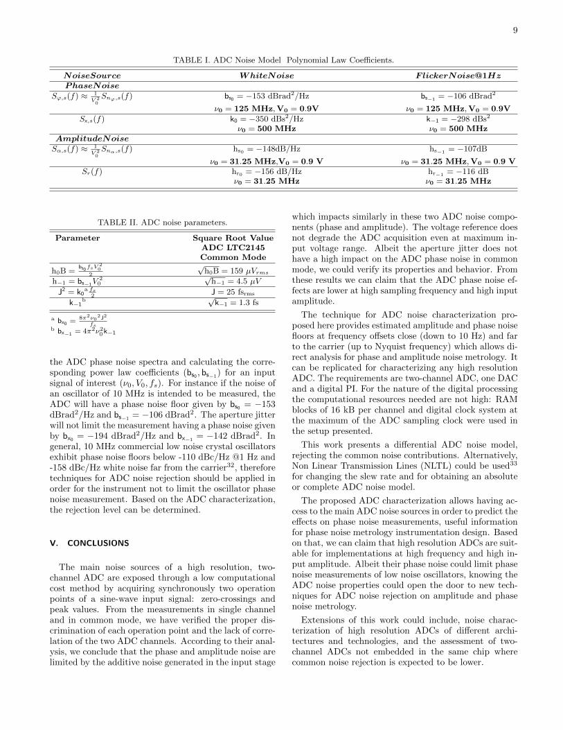
TABLE I. ADC Noise Model Polynomial Law Coefficients.
NoiseSource WhiteNoise F lickerNoise@1HzPhaseNoise
Sϕ,s(f) ≈ 1V 20
Snϕ,s(f) bs0 = −153 dBrad2/Hz bs−1 = −106 dBrad2
ν0 = 125 MHz,V0 = 0.9V ν0 = 125 MHz,V0 = 0.9VSx,s(f) k0 = −350 dBs2/Hz k−1 = −298 dBs2
ν0 = 500 MHz ν0 = 500 MHzAmplitudeNoiseSα,s(f) ≈ 1
V 20
Snα,s(f) hs0 = −148dB/Hz hs−1 = −107dB
ν0 = 31.25 MHz,V0 = 0.9 V ν0 = 31.25 MHz,V0 = 0.9 VSr(f) hr0 = −156 dB/Hz hr−1 = −116 dB
ν0 = 31.25 MHz ν0 = 31.25 MHz
TABLE II. ADC noise parameters.
Parameter Square Root ValueADC LTC2145Common Mode
h0B =bs0fsV
20
2
√h0B = 159 µVrms
h−1 = bs−1V20
√h−1 = 4.5 µV
J2 = k0a fs
2J = 25 fsrms
k−1b √
k−1 = 1.3 fs
a bx0 = 8π2ν02J2
fsb bx−1 = 4π2ν20k−1
the ADC phase noise spectra and calculating the corre-sponding power law coefficients (bs0 , bs−1) for an inputsignal of interest (ν0, V0, fs). For instance if the noise ofan oscillator of 10 MHz is intended to be measured, theADC will have a phase noise floor given by bs0 = −153dBrad2/Hz and bs−1 = −106 dBrad2. The aperture jitterwill not limit the measurement having a phase noise givenby bx0 = −194 dBrad2/Hz and bx−1 = −142 dBrad2. Ingeneral, 10 MHz commercial low noise crystal oscillatorsexhibit phase noise floors below -110 dBc/Hz @1 Hz and-158 dBc/Hz white noise far from the carrier32, thereforetechniques for ADC noise rejection should be applied inorder for the instrument not to limit the oscillator phasenoise measurement. Based on the ADC characterization,the rejection level can be determined.
V. CONCLUSIONS
The main noise sources of a high resolution, two-channel ADC are exposed through a low computationalcost method by acquiring synchronously two operationpoints of a sine-wave input signal: zero-crossings andpeak values. From the measurements in single channeland in common mode, we have verified the proper dis-crimination of each operation point and the lack of corre-lation of the two ADC channels. According to their anal-ysis, we conclude that the phase and amplitude noise arelimited by the additive noise generated in the input stage
which impacts similarly in these two ADC noise compo-nents (phase and amplitude). The voltage reference doesnot degrade the ADC acquisition even at maximum in-put voltage range. Albeit the aperture jitter does nothave a high impact on the ADC phase noise in commonmode, we could verify its properties and behavior. Fromthese results we can claim that the ADC phase noise ef-fects are lower at high sampling frequency and high inputamplitude.
The technique for ADC noise characterization pro-posed here provides estimated amplitude and phase noisefloors at frequency offsets close (down to 10 Hz) and farto the carrier (up to Nyquist frequency) which allows di-rect analysis for phase and amplitude noise metrology. Itcan be replicated for characterizing any high resolutionADC. The requirements are two-channel ADC, one DACand a digital PI. For the nature of the digital processingthe computational resources needed are not high: RAMblocks of 16 kB per channel and digital clock system atthe maximum of the ADC sampling clock were used inthe setup presented.
This work presents a differential ADC noise model,rejecting the common noise contributions. Alternatively,Non Linear Transmission Lines (NLTL) could be used33
for changing the slew rate and for obtaining an absoluteor complete ADC noise model.
The proposed ADC characterization allows having ac-cess to the main ADC noise sources in order to predict theeffects on phase noise measurements, useful informationfor phase noise metrology instrumentation design. Basedon that, we can claim that high resolution ADCs are suit-able for implementations at high frequency and high in-put amplitude. Albeit their phase noise could limit phasenoise measurements of low noise oscillators, knowing theADC noise properties could open the door to new tech-niques for ADC noise rejection on amplitude and phasenoise metrology.
Extensions of this work could include, noise charac-terization of high resolution ADCs of different archi-tectures and technologies, and the assessment of two-channel ADCs not embedded in the same chip wherecommon noise rejection is expected to be lower.
10
ACKNOWLEDGMENTS
This work has been funded by the EMRP program(IND55 Mclocks). The EMRP is jointly funded by theEMRP participating countries within EURAMET andthe European Union. This work was partly supportedby the ANR Programme d’Investissement d’Avenir (PIA)under the Oscillator IMP project and the First-TF net-work, and by grants from the Region Bourgogne FrancheComte intended to support the PIA.
REFERENCES
1J. Grove, J. Hein, P. Schweiger J. Retta, W. Solbrig, andS.R. Stein. Direct-digital phase-noise measurement. In Proc.2004 IEEE International Ultrasonics, Ferroelectrics and Fre-quency Control Joint 50th Anniversary Conference, pages 287–291, Montral, Canada, 2004.
2M. Uchino and K. Mochizuki. Frequency stability measuringtechnique using digital signal processing. Electronics and Com-munications in Japan, 87(1):21–33, 2004.
3L.B. Ruppalt, D.R. McKinstry, K.C. Lauritzen, A.K. Wu, S.A.Phillips, and S.H. Talisa. Simultaneous digital measurement ofphase and amplitude noise. In Proc. Frequency Control Sympo-sium (FCS), 2010 IEEE International, pages 97–102, NewportBeach, CA, USA, 2010.
4K. Gheen. Pulsed phase noise measurements. application noteR&S FSWP. http://www.rohde-schwarz.com/appnote/1EF94,May 2016.
5M. Kazda, V. Gerginov, N. Huntemann, B. Lipphardt, andS. Weyers. Phase Analysis for Frequency Standards in the Mi-crowave and Optical Domains. IEEE Transactions on Ultrason-ics, Ferroelectrics, and Frequency Control, 63(7):970–974, July2016.
6K. Mochizuki, M. Uchino, and T. Morikawa. Frequency-stabilitymeasurement system using high-speed adcs and digital signalprocessing. IEEE Trans. Instrumentation and Measurement,56(5):1887–1893, Oct. 2007.
7C. W. Nelson and D. A. Howe. A sub-sampling digital pm/amnoise measurement system. In Proc. Frequency Control Sym-posium (FCS), 2012 IEEE International, Baltimore, MD, USA,May 2012.
8J.A. Sherman and R. Jordens. Oscillator metrology with softwaredefined radio. Review of Scientific Instruments, 87, May 2016.Rev. Sci. Instrum. 87, 054711 (2016); doi: 10.1063/1.4950898.
9F.L. Walls, S.R. Stein, J.E. Gray, and D.J. Glaze. Design con-siderations in state-of-the-art signal processing and phase noisemeasurement systems. In Proc. 30th Annual Symposium on Fre-quency Control., Atlantic City, NJ, USA, June 1976. IEEE.
10W.F. Walls. Cross-correlation phase noise measurements. InProc. 46th Frequency Control Symposium., Hershey, PA, USA,May 1992. IEEE.
11J. Li, E. Ferre-Pikal, C. Nelson, and F.L. Walls. Review ofpm and am noise measurement systems. In Proc. Interna-tional Conference on Microwave and Millimeter Wave Technol-ogy. ICMMT ’98., Beijing, China, Aug. 1998. IEEE.
12E. Rubiola and F. Vernotte. The cross-spectrum experimentalmethod. arXiv:1003.0113v1 [physics.ins-det], Feb. 2010.
13C.W. Nelson, A. Hati, and D.A. Howe. Phase inversionand collapse of the cross-spectral function. arXiv:1307.6605v1[physics.ins-det], Jul. 2013.
14Y. Gruson, V. Giordano, U.L. Rohde, A.K. Poddar, and E. Ru-biola. Cross-Spectrum PM Noise Measurement, Thermal En-ergy, and Metamaterial Filters. IEEE Transactions on Ultrason-
ics, Ferroelectrics, and Frequency Control, 64(3):634–642, March2017.
15J. Mitola III. Software Radio Architecture: Object-Oriented Ap-proaches to Wireless Systems Engineering. John Wiley & Sons,Inc., New York, NY, USA, 2000.
16J. Blair. Histogram Measurement of ADC Nonlinearities UsingSine Waves. IEEE Transactions on Instrumentation and Mea-surement, 43(3):373–383, June 1994.
17R.C. Martins and A.C. Serra. ADC characterization by usingthe histogram test stimulated by Gaussian noise. Theory andexperimental results. Elsevier Measurement, 27:291–300, 2000.
18G. Chiorboli, M. Fontanili, and C. Morandi. A New Methodfor Estimating the Aperture Uncertainty of A/D Converters.IEEE Trans. Instrumentation and Measurement, 47(1):61–64,Feb. 1998.
19M. Shinagawa, Y. Akazawa, and T. Wakimoto. Jitter Analysisof High-speed Sampling Systems. IEEE Journal of Solid-StateCircuits, 25(1):220–224, Feb. 1990.
20F. Overney, A. Rfenacht, J.-P. Braun, B. Jeanneret, and P.S.Wright. Characterization of Metrological Grade Analog-to-Digital Converters Using a Programmable Josephson VoltageStandard. IEEE Transactions on Instrumentation and Measure-ment, 60(7):2172–2177, July 2011.
21P.-Y. Bourgeois, T. Imaike, G. Goavec-Merou, and E. Rubiola.Noise in high-speed digital-to-analog converters. In Proc. Fre-quency Control Symposium & the European Frequency and TimeForum (FCS), 2015 Joint Conference of the IEEE International,Denver, CO, USA, April 2015.
22E. Rubiola. Phase Noise and Frequency Stability in Oscillators.Cambridge University Press, New York, NY, USA, 2009.
23A. Konczakowska, B.M. Wilamowski, and J.D. Irwin. The Indus-trial Electronics Handbook, Fundamentals of Industrial Electron-ics. CRC Press Taylor & Francis Group, Boca Raton, FL, USA,2 edition, 2011. Chapter 11. Noise in Semiconductor Devices.
24B. Brannon and A. Barlow. Aperture Uncertainty and ADCSystem Performance. Application Note AN-501, Analog Devices,Norwood, MA, USA, 2006.
25M. Lohning and G. Fettweis. The effects of aperture jitter andclock jitter in wideband ADCs. Computer Standards & Inter-faces, (29):11–18, 2007.
26M. Oljaca and B. Baker. How the voltage reference affects ADCperformance, Part 2. Analog Applications Journal 3Q, TexasInstruments, 2009.
27B. Widrow and I. Kollar. Quantization Noise. Roundoff Errorin Digital Computation, Signal Processing, Control, and Com-munications. Cambridge University Press, New York, NY, USA,2008.
28C.E. Calosso and E. Rubiola. Phase noise and jitter in digitalelectronics. arXiv:1701.00094 [physics.ins-det], Dec. 2016.
29Red Pitaya. Documentation and technical information.http://redpitaya.readthedocs.io/en/latest/.
30Linear Technology. ADC LTC2145 datasheet. Techni-cal documentation, Linear Technology Corporation, 2011.http://cds.linear.com/docs/en/datasheet/21454314fa.pdf.
31E. Rubiola. Tutorial on the double balanced mixer.arXiv:physics/0608211v1 [physics.ins-det], Aug. 2006.
32Wenzel Associates Inc. Standard Specifications and Part Num-bers. http://www.wenzel.com/product/crystal-oscillators/oven-controlled/1mhz-to-25mhz/.
33B. Francois, C.E. Calosso, J.M. Danet, and R. Boudot. Alow phase noise microwave frequency synthesis for a high-performance cesium vapor cell atomic clock. Review of ScientificInstruments, 85:094709, 2014.