nhd-0220dzw-ay5 - newhaven display international, inc. · nhd-0220dzw-ay5 . oled display module ....
TRANSCRIPT
NHD-0220DZW-AY5 OLED Display Module
NHD- Newhaven Display 0220- 2 Lines x 20 Characters DZW- OLED A- Transflective Y- Emitting Color: Yellow 5- +5V Power Supply RoHS Compliant
Newhaven Display International, Inc.
2661 Galvin Ct. Elgin IL, 60124
Ph: 847-844-8795 Fax: 847-844-8796
www.newhavendisplay.com [email protected] [email protected]
[2]
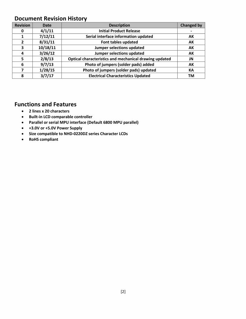
Document Revision History Revision Date Description Changed by
0 4/1/11 Initial Product Release - 1 7/12/11 Serial interface information updated AK 2 8/31/11 Font tables updated AK 3 10/18/11 Jumper selections updated AK 4 3/26/12 Jumper selections updated AK 5 2/8/13 Optical characteristics and mechanical drawing updated JN 6 9/7/13 Photo of jumpers (solder pads) added AK 7 1/28/15 Photo of jumpers (solder pads) updated KA 8 3/7/17 Electrical Characteristics Updated TM
Functions and Features • 2 lines x 20 characters • Built-in LCD comparable controller • Parallel or serial MPU interface (Default 6800 MPU parallel) • +3.0V or +5.0V Power Supply • Size compatible to NHD-0220DZ series Character LCDs • RoHS compliant
PROPRI
ETARY
1 2 3 4 5 6
A
B
C
D
B
C
D
1 2 3 4 5 6
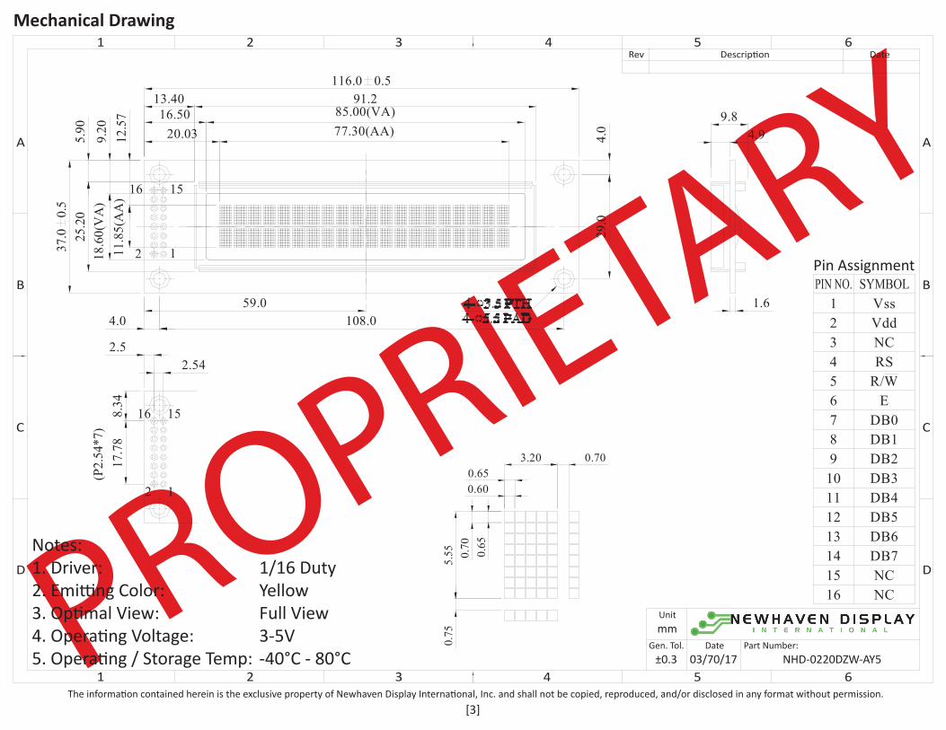
Mechanical Drawing
A
[3]The information contained herein is the exclusive property of Newhaven Display International, Inc. and shall not be copied, reproduced, and/or disclosed in any format without permission.
NHD-0220DZW-AY503/70/17Date
Unit
Part Number:
mmGen. Tol.
±0.3
Rev Description Date
Notes:1. Driver: 1/16 Duty2. Emitting Color: Yellow3. Optimal View: Full View4. Operating Voltage: 3-5V5. Operating / Storage Temp: -40°C - 80°C
0.600.65
3.20 0.70
0.65
0.70
5.55
0.75
2.52.54
8.34
17.7
8(P
2.54
*7)
1
15
2
16
1.6
4.99.8
9.20
11.8
5(A
A)
18.6
0(V
A)
20.0316.50
13.40
77.30(AA)85.00(VA)
91.2
59.04.0 108.0
12.5
7
5.90
25.2
037
.00.
5116.0 0.5
4.0
29.0
12
1516
DB412
1413 DB6
DB5
Vss1
E7
1110
89
DB3DB2DB1DB0
4
65
32
R/WRSNCVdd
DB7NC15NC16
Pin Assignment
[4]
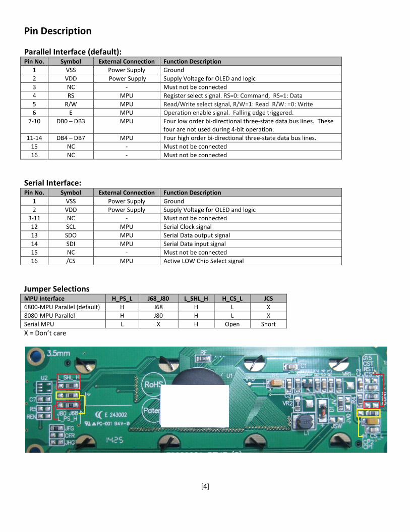
Pin Description Parallel Interface (default): Pin No. Symbol External Connection Function Description
1 VSS Power Supply Ground 2 VDD Power Supply Supply Voltage for OLED and logic 3 NC - Must not be connected 4 RS MPU Register select signal. RS=0: Command, RS=1: Data 5 R/W MPU Read/Write select signal, R/W=1: Read R/W: =0: Write 6 E MPU Operation enable signal. Falling edge triggered.
7-10 DB0 – DB3 MPU Four low order bi-directional three-state data bus lines. These four are not used during 4-bit operation.
11-14 DB4 – DB7 MPU Four high order bi-directional three-state data bus lines. 15 NC - Must not be connected 16 NC - Must not be connected
Serial Interface: Pin No. Symbol External Connection Function Description
1 VSS Power Supply Ground 2 VDD Power Supply Supply Voltage for OLED and logic
3-11 NC - Must not be connected 12 SCL MPU Serial Clock signal 13 SDO MPU Serial Data output signal 14 SDI MPU Serial Data input signal 15 NC - Must not be connected 16 /CS MPU Active LOW Chip Select signal
Jumper Selections MPU Interface H_PS_L J68_J80 L_SHL_H H_CS_L JCS 6800-MPU Parallel (default) H J68 H L X 8080-MPU Parallel H J80 H L X Serial MPU L X H Open Short X = Don’t care
[5]
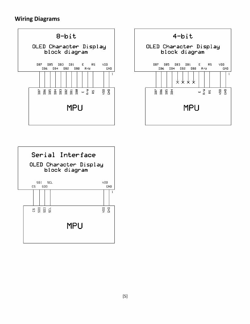
Wiring Diagrams
[6]
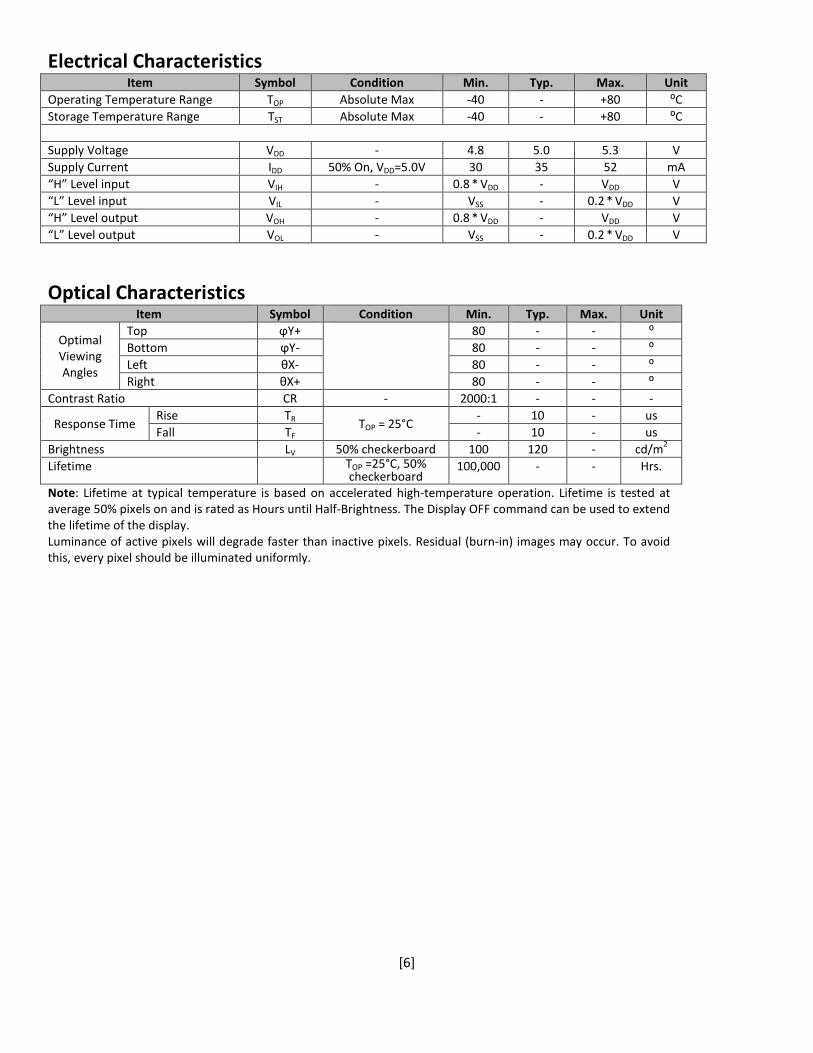
Electrical Characteristics Item Symbol Condition Min. Typ. Max. Unit
Operating Temperature Range TOP Absolute Max -40 - +80 ⁰C Storage Temperature Range TST Absolute Max -40 - +80 ⁰C
Supply Voltage VDD - 4.8 5.0 5.3 V Supply Current IDD 50% On, VDD=5.0V 30 35 52 mA “H” Level input VIH - 0.8 * VDD - VDD V “L” Level input VIL - VSS - 0.2 * VDD V “H” Level output VOH - 0.8 * VDD - VDD V “L” Level output VOL - VSS - 0.2 * VDD V
Optical Characteristics Item Symbol Condition Min. Typ. Max. Unit
Optimal Viewing Angles
Top ϕY+
80 - - ⁰ Bottom ϕY- 80 - - ⁰ Left θX- 80 - - ⁰ Right θX+ 80 - - ⁰
Contrast Ratio CR - 2000:1 - - -
Response Time Rise TR
TOP = 25°C - 10 - us
Fall TF - 10 - us Brightness LV 50% checkerboard 100 120 - cd/m2 Lifetime TOP =25°C, 50%
checkerboard 100,000 - - Hrs.
Note: Lifetime at typical temperature is based on accelerated high-temperature operation. Lifetime is tested at average 50% pixels on and is rated as Hours until Half-Brightness. The Display OFF command can be used to extend the lifetime of the display. Luminance of active pixels will degrade faster than inactive pixels. Residual (burn-in) images may occur. To avoid this, every pixel should be illuminated uniformly.
[7]
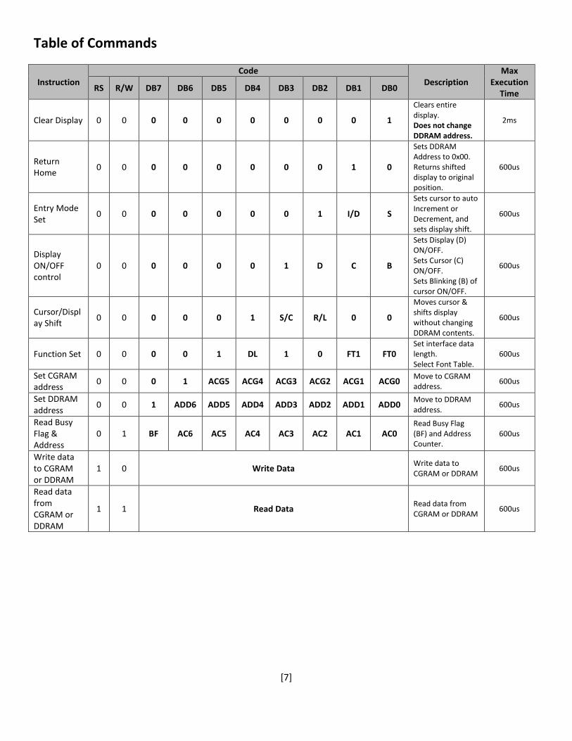
Table of Commands
Instruction Code
Description Max
Execution Time RS R/W DB7 DB6 DB5 DB4 DB3 DB2 DB1 DB0
Clear Display 0 0 0 0 0 0 0 0 0 1
Clears entire display. Does not change DDRAM address.
2ms
Return Home 0 0 0 0 0 0 0 0 1 0
Sets DDRAM Address to 0x00. Returns shifted display to original position.
600us
Entry Mode Set 0 0 0 0 0 0 0 1 I/D S
Sets cursor to auto Increment or Decrement, and sets display shift.
600us
Display ON/OFF control
0 0 0 0 0 0 1 D C B
Sets Display (D) ON/OFF. Sets Cursor (C) ON/OFF. Sets Blinking (B) of cursor ON/OFF.
600us
Cursor/Display Shift 0 0 0 0 0 1 S/C R/L 0 0
Moves cursor & shifts display without changing DDRAM contents.
600us
Function Set 0 0 0 0 1 DL 1 0 FT1 FT0 Set interface data length. Select Font Table.
600us
Set CGRAM address 0 0 0 1 ACG5 ACG4 ACG3 ACG2 ACG1 ACG0 Move to CGRAM
address. 600us
Set DDRAM address 0 0 1 ADD6 ADD5 ADD4 ADD3 ADD2 ADD1 ADD0 Move to DDRAM
address. 600us
Read Busy Flag & Address
0 1 BF AC6 AC5 AC4 AC3 AC2 AC1 AC0 Read Busy Flag (BF) and Address Counter.
600us
Write data to CGRAM or DDRAM
1 0 Write Data Write data to CGRAM or DDRAM 600us
Read data from CGRAM or DDRAM
1 1 Read Data Read data from CGRAM or DDRAM 600us
[8]
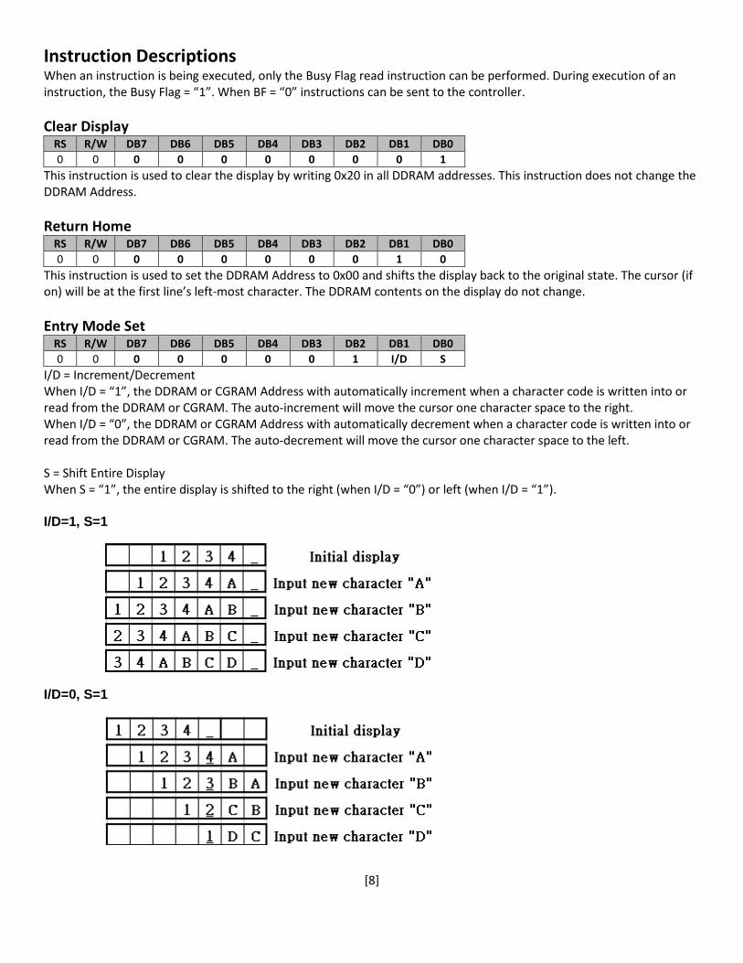
Instruction Descriptions When an instruction is being executed, only the Busy Flag read instruction can be performed. During execution of an instruction, the Busy Flag = “1”. When BF = “0” instructions can be sent to the controller. Clear Display
RS R/W DB7 DB6 DB5 DB4 DB3 DB2 DB1 DB0 0 0 0 0 0 0 0 0 0 1
This instruction is used to clear the display by writing 0x20 in all DDRAM addresses. This instruction does not change the DDRAM Address. Return Home
RS R/W DB7 DB6 DB5 DB4 DB3 DB2 DB1 DB0 0 0 0 0 0 0 0 0 1 0
This instruction is used to set the DDRAM Address to 0x00 and shifts the display back to the original state. The cursor (if on) will be at the first line’s left-most character. The DDRAM contents on the display do not change. Entry Mode Set
RS R/W DB7 DB6 DB5 DB4 DB3 DB2 DB1 DB0 0 0 0 0 0 0 0 1 I/D S
I/D = Increment/Decrement When I/D = “1”, the DDRAM or CGRAM Address with automatically increment when a character code is written into or read from the DDRAM or CGRAM. The auto-increment will move the cursor one character space to the right. When I/D = “0”, the DDRAM or CGRAM Address with automatically decrement when a character code is written into or read from the DDRAM or CGRAM. The auto-decrement will move the cursor one character space to the left. S = Shift Entire Display When S = “1”, the entire display is shifted to the right (when I/D = “0”) or left (when I/D = “1”). I/D=1, S=1
I/D=0, S=1
[9]
Display ON/OFF RS R/W DB7 DB6 DB5 DB4 DB3 DB2 DB1 DB0 0 0 0 0 0 0 1 D C B
D = Display ON/OFF When D = “1”, the display is turned ON. When D = “0”, the display is turned OFF. Contents in DDRAM are not changed. C = Cursor ON/OFF When C = “1”, the cursor is displayed. The cursor is displayed as 5 dots on the 8th line of a character. When C = “0”, the cursor is OFF. B = Blinking Cursor When B = “1”, the entire character specified by the cursor blinks at a speed of 409.6ms intervals. When B = “0”, the character does not blink, the cursor remains on. Cursor/Display Shift
RS R/W DB7 DB6 DB5 DB4 DB3 DB2 DB1 DB0 0 0 0 0 0 1 S/C R/L 0 0
S/C R/L Shift Function 0 0 Shifts the cursor position to the left (AC is decremented by 1). 0 1 Shifts the cursor position to the right (AC is incremented by 1). 1 0 Shifts the entire display to the left. The cursor follows the display shift. 1 1 Shifts the entire display to the right. The cursor follows the display shift.
When the display is shifted repeatedly, each line moves only horizontally. The second line display does not shift into the first line. The Address Counter does not change during a Display Shift. Function Set
RS R/W DB7 DB6 DB5 DB4 DB3 DB2 DB1 DB0 0 0 0 0 1 DL 1 0 FT1 FT0
DL = Interface Data Length When DL = “1”, the data is sent or received in 8-bit length via DB7...DB0. When DL = “0”, the data is sent or received in 4-bit length via DB7...DB4. When the 4-bit data length is used, the data must be sent or received in two consecutive writes/reads to combine the data into full 8-bits. FT1, FT0 = Font Table Selection
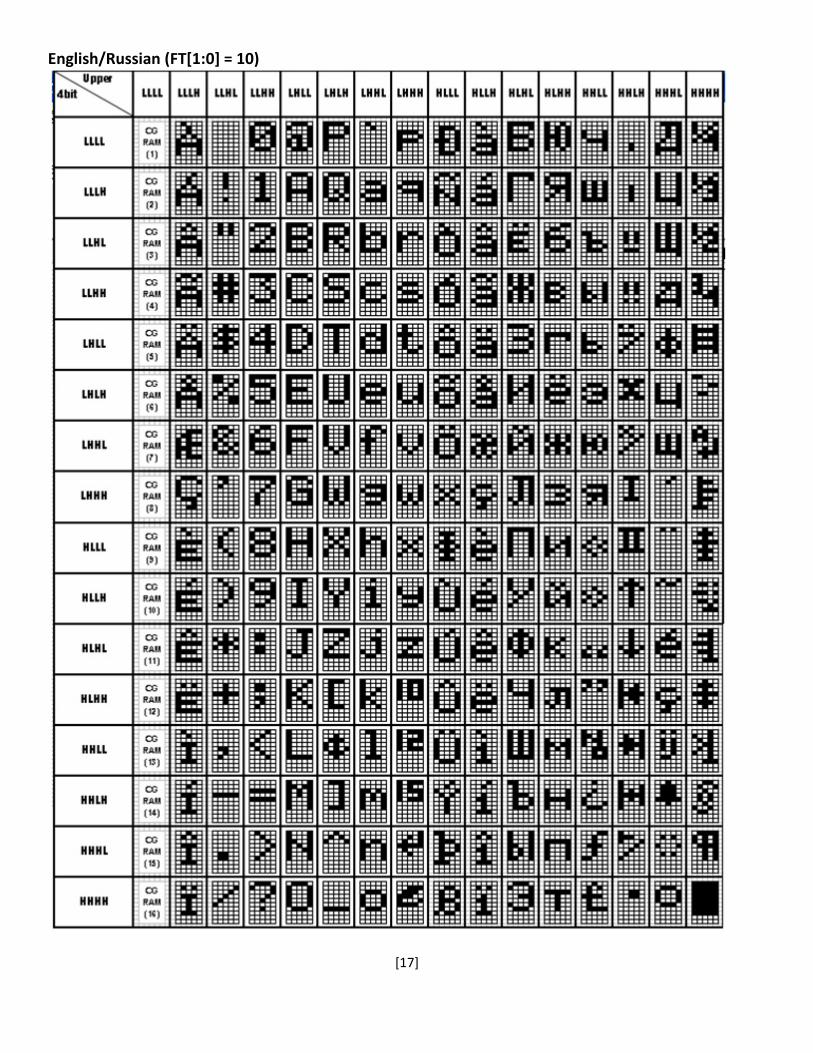
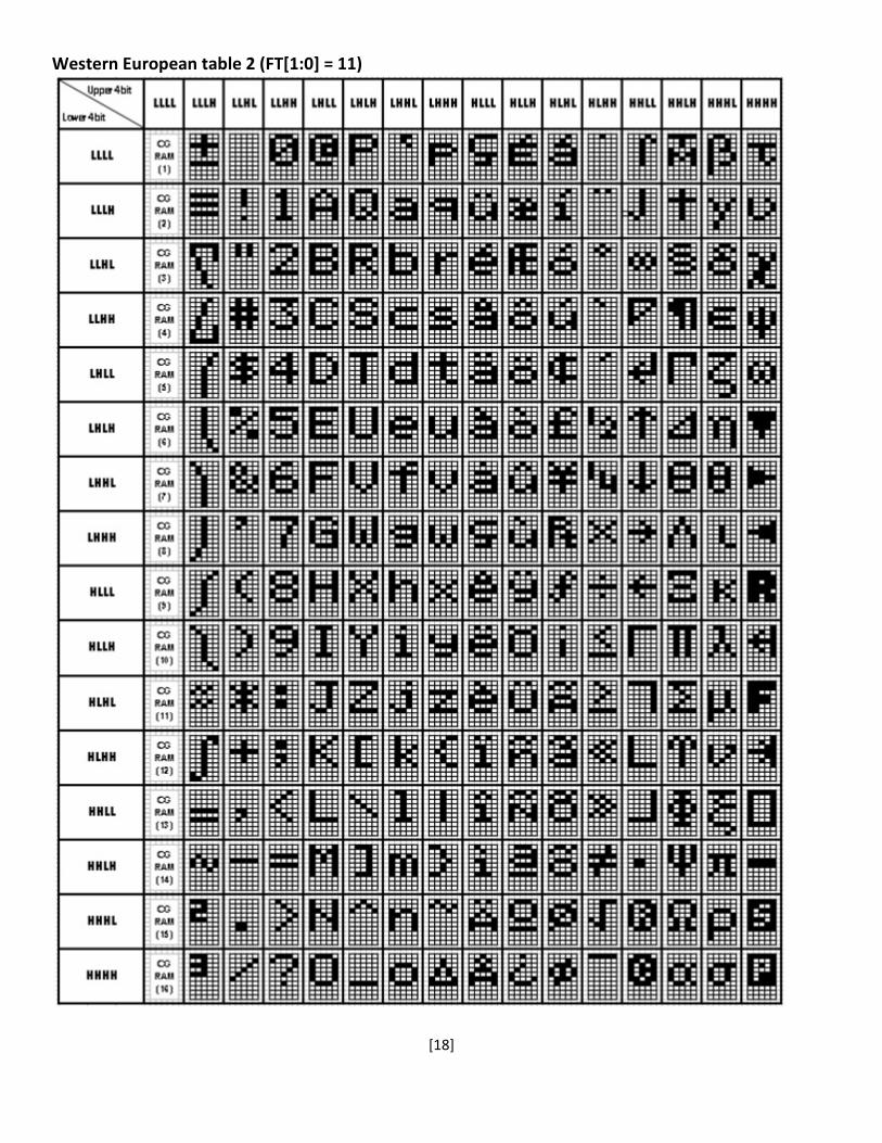
FT1 FT0 Font Table 0 0 English / Japanese 0 1 Western European #1 1 0 English / Russian 1 1 Western European #2
Note: Changing the font table during operation will immediately change any data currently on the display to the corresponding character on the newly selected font table.
[10]
Set CGRAM Address RS R/W DB7 DB6 DB5 DB4 DB3 DB2 DB1 DB0 0 0 0 1 ACG5 ACG4 ACG3 ACG2 ACG1 ACG0
This instruction is used to set the CGRAM address into the Address Counter. Data can then be written to or read from the CGRAM locations. See section: “How to use CGRAM”. ACG5...ACG0 is the binary CGRAM address. Set DDRAM Address
RS R/W DB7 DB6 DB5 DB4 DB3 DB2 DB1 DB0 0 0 1 ADD6 ADD5 ADD4 ADD3 ADD2 ADD1 ADD0
This instruction is used to set the DDRAM address into the Address Counter. Data can then be written to or read from the DDRAM locations. ADD6...ADD0 is the binary DDRAM address. Line 1 = Address 0x00 through 0x13 Line 2 = Address 0x40 through 0x53
1 2 3 4 5 6 7 8 9 10 11 12 13 14 15 16 17 18 19 20 00 01 02 03 04 05 06 07 08 09 0A 0B 0C 0D 0E 0F 10 11 12 13 40 41 42 43 44 45 46 47 48 49 4A 4B 4C 4D 4E 4F 50 51 52 53
Read Busy Flag and Address Counter
RS R/W DB7 DB6 DB5 DB4 DB3 DB2 DB1 DB0 0 1 BF AC6 AC5 AC4 AC3 AC2 AC1 AC0
This instruction is used to read the Busy Flag (BF) to indicate if the display controller is performing an internal operation. The Address Counter is read simultaneously with checking the Busy Flag. When BF = “1”, the controller is busy and the next instruction will be ignored. When BF = “0”, the controller is not busy and is ready to accept instructions. AC6...AC0 is the binary location of either the CGRAM or DDRAM current address. Write Data to CGRAM or DDRAM
RS R/W DB7 DB6 DB5 DB4 DB3 DB2 DB1 DB0 1 0 Write Data
This instruction is used to write 8-bits of data to the CGRAM or DDRAM at the current address counter. After the write is complete, the address is automatically incremented or decremented by 1 according to the Entry Mode. Read Data from CGRAM or DDRAM
RS R/W DB7 DB6 DB5 DB4 DB3 DB2 DB1 DB0 1 1 Read Data
This instruction is used to read 8-bits of data to the CGRAM or DDRAM at the current address counter. After the read is complete, the address is automatically incremented or decremented by 1 according to the Entry Mode. The Set CGRAM Address or Set DDRAM Address Instruction must be executed before this instruction can be performed, otherwise the first Read Data will not be valid.
[11]
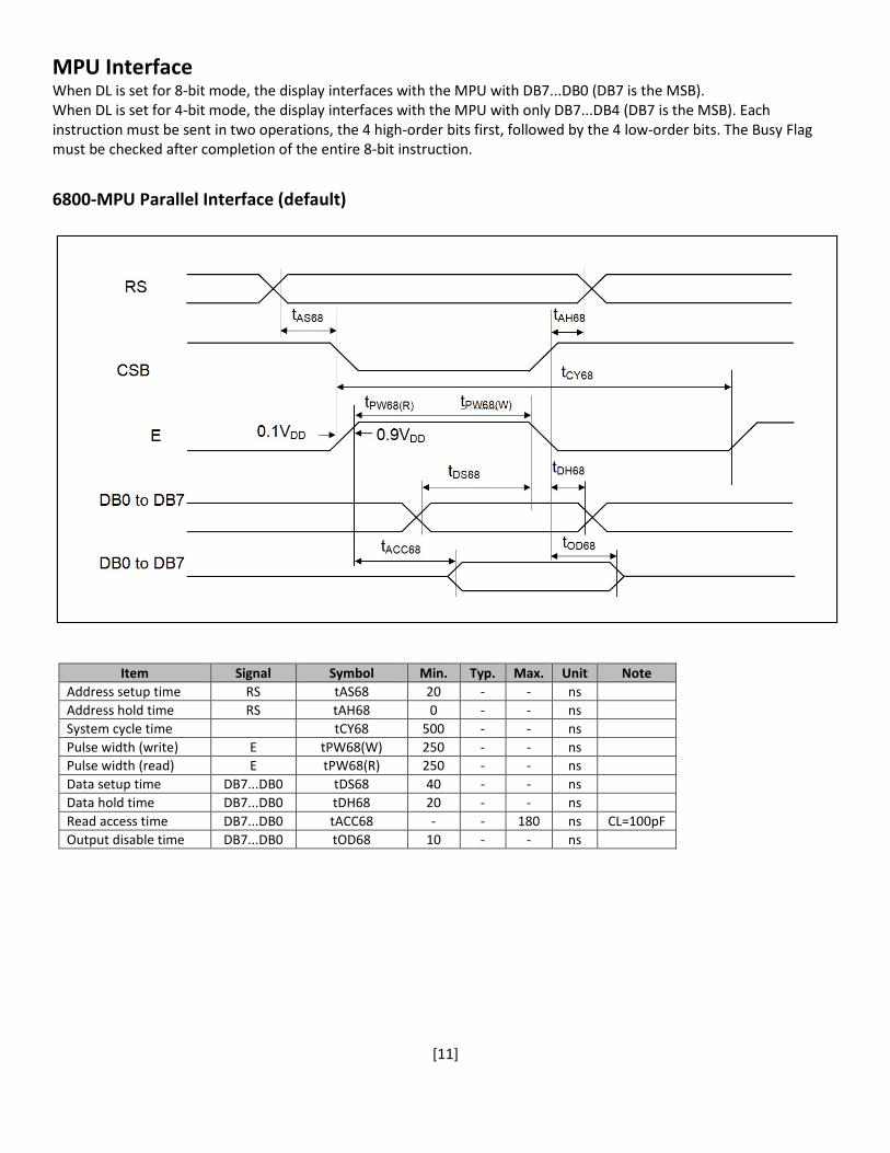
MPU Interface When DL is set for 8-bit mode, the display interfaces with the MPU with DB7...DB0 (DB7 is the MSB). When DL is set for 4-bit mode, the display interfaces with the MPU with only DB7...DB4 (DB7 is the MSB). Each instruction must be sent in two operations, the 4 high-order bits first, followed by the 4 low-order bits. The Busy Flag must be checked after completion of the entire 8-bit instruction.
6800-MPU Parallel Interface (default)
Item Signal Symbol Min. Typ. Max. Unit Note Address setup time RS tAS68 20 - - ns Address hold time RS tAH68 0 - - ns System cycle time tCY68 500 - - ns Pulse width (write) E tPW68(W) 250 - - ns Pulse width (read) E tPW68(R) 250 - - ns Data setup time DB7...DB0 tDS68 40 - - ns Data hold time DB7...DB0 tDH68 20 - - ns Read access time DB7...DB0 tACC68 - - 180 ns CL=100pF Output disable time DB7...DB0 tOD68 10 - - ns
[12]
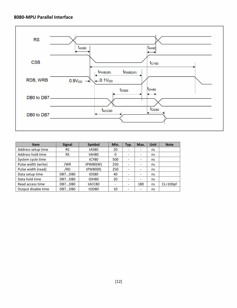
8080-MPU Parallel Interface
Item Signal Symbol Min. Typ. Max. Unit Note Address setup time RS tAS80 20 - - ns Address hold time RS tAH80 0 - - ns System cycle time tCY80 500 - - ns Pulse width (write) /WR tPW80(W) 250 - - ns Pulse width (read) /RD tPW80(R) 250 - - ns Data setup time DB7...DB0 tDS80 40 - - ns Data hold time DB7...DB0 tDH80 20 - - ns Read access time DB7...DB0 tACC80 - - 180 ns CL=100pF Output disable time DB7...DB0 tOD80 10 - - ns
[13]
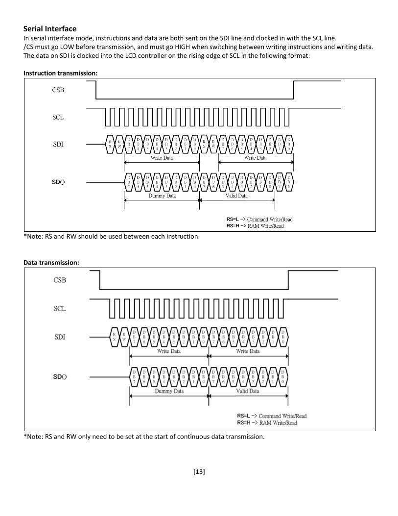
Serial Interface In serial interface mode, instructions and data are both sent on the SDI line and clocked in with the SCL line. /CS must go LOW before transmission, and must go HIGH when switching between writing instructions and writing data. The data on SDI is clocked into the LCD controller on the rising edge of SCL in the following format: Instruction transmission:
*Note: RS and RW should be used between each instruction. Data transmission:
*Note: RS and RW only need to be set at the start of continuous data transmission.
[14]
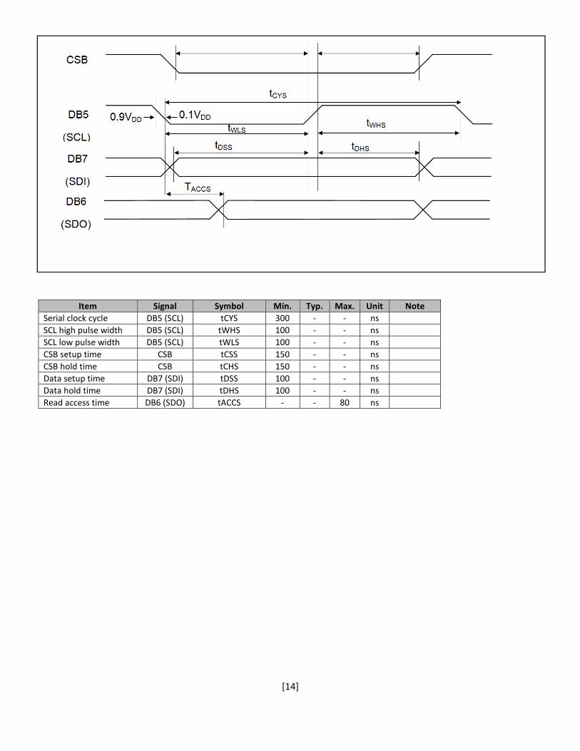
Item Signal Symbol Min. Typ. Max. Unit Note Serial clock cycle DB5 (SCL) tCYS 300 - - ns SCL high pulse width DB5 (SCL) tWHS 100 - - ns SCL low pulse width DB5 (SCL) tWLS 100 - - ns CSB setup time CSB tCSS 150 - - ns CSB hold time CSB tCHS 150 - - ns Data setup time DB7 (SDI) tDSS 100 - - ns Data hold time DB7 (SDI) tDHS 100 - - ns Read access time DB6 (SDO) tACCS - - 80 ns
[15]
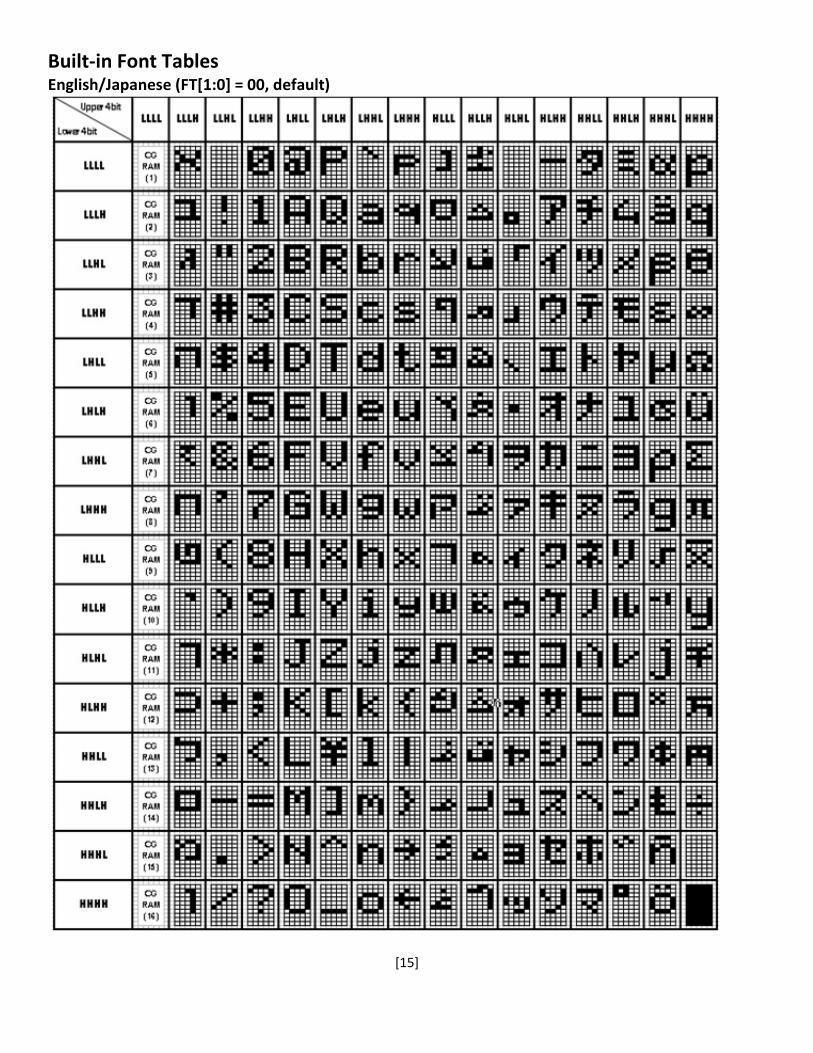
Built-in Font Tables English/Japanese (FT[1:0] = 00, default)
[16]
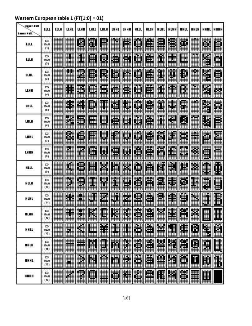
Western European table 1 (FT[1:0] = 01)
[17]
English/Russian (FT[1:0] = 10)
[18]
Western European table 2 (FT[1:0] = 11)
[19]
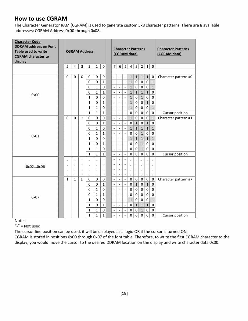
How to use CGRAM The Character Generator RAM (CGRAM) is used to generate custom 5x8 character patterns. There are 8 available addresses: CGRAM Address 0x00 through 0x08. Character Code DDRAM address on Font Table used to write CGRAM character to display
CGRAM Address
Character Patterns (CGRAM data)
Character Patterns (CGRAM data)
5 4 3 2 1 0 7 6 5 4 3 2 1 0
0x00
0 0 0 0 0 0 - - - 1 1 1 1 0 Character pattern #0 0 0 1 - - - 1 0 0 0 1 0 1 0 - - - 1 0 0 0 1 0 1 1 - - - 1 1 1 1 0 1 0 0 - - - 1 0 1 0 0 1 0 1 - - - 1 0 0 1 0 1 1 0 - - - 1 0 0 0 1 1 1 1 - - - 0 0 0 0 0 Cursor position
0x01
0 0 1 0 0 0 - - - 1 0 0 0 1 Character pattern #1 0 0 1 - - - 0 1 0 1 0 0 1 0 - - - 1 1 1 1 1 0 1 1 - - - 0 0 1 0 0 1 0 0 - - - 1 1 1 1 1 1 0 1 - - - 0 0 1 0 0 1 1 0 - - - 0 0 1 0 0 1 1 1 - - - 0 0 0 0 0 Cursor position
0x02...0x06
.
.
.
.
.
.
.
.
.
.
.
.
.
.
.
.
.
.
.
.
.
.
.
.
- - - -
- - - -
- - - -
.
.
.
.
.
.
.
.
.
.
.
.
.
.
.
.
.
.
.
.
0x07
1 1 1 0 0 0 - - - 0 0 0 0 0 Character pattern #7 0 0 1 - - - 0 1 0 1 0 0 1 0 - - - 0 0 0 0 0 0 1 1 - - - 0 0 0 0 0 1 0 0 - - - 1 0 0 0 1 1 0 1 - - - 0 1 1 1 0 1 1 0 - - - 0 0 1 0 0 1 1 1 - - - 0 0 0 0 0 Cursor position
Notes: “-” = Not used The cursor line position can be used, it will be displayed as a logic-OR if the cursor is turned ON. CGRAM is stored in positions 0x00 through 0x07 of the font table. Therefore, to write the first CGRAM character to the display, you would move the cursor to the desired DDRAM location on the display and write character data 0x00.
[20]
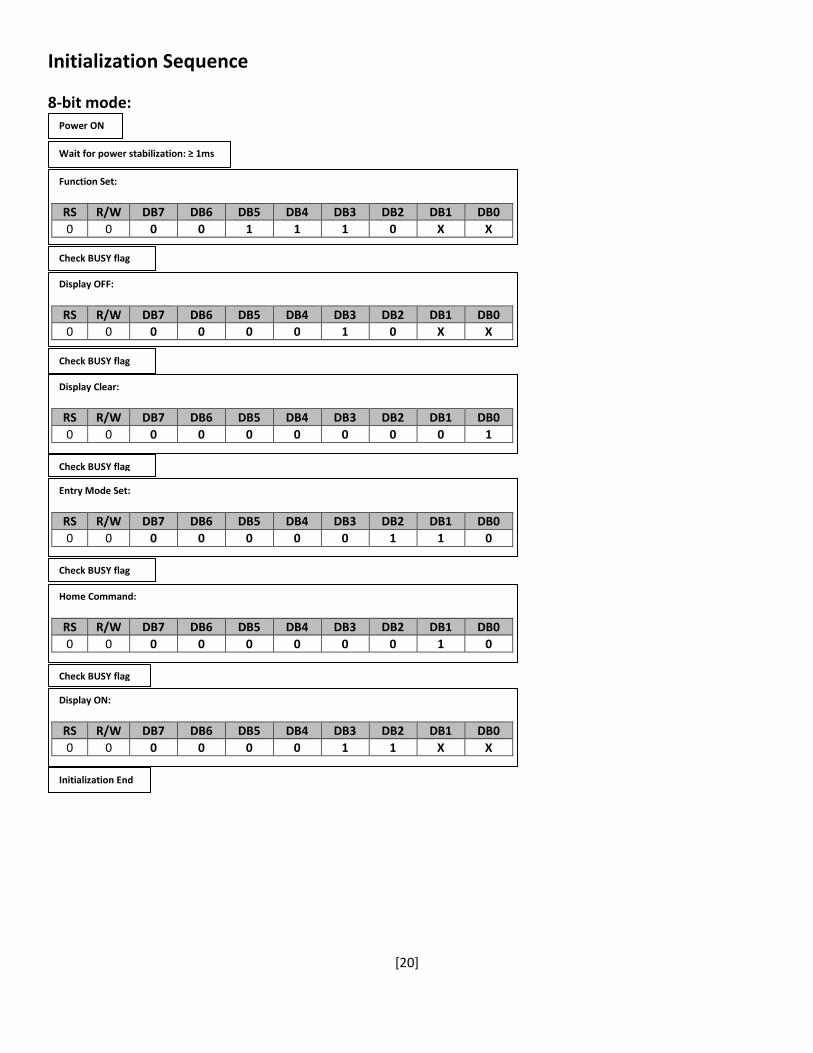
Initialization Sequence 8-bit mode:
Initialization End
Display ON:
RS R/W DB7 DB6 DB5 DB4 DB3 DB2 DB1 DB0 0 0 0 0 0 0 1 1 X X
Check BUSY flag
Home Command:
RS R/W DB7 DB6 DB5 DB4 DB3 DB2 DB1 DB0 0 0 0 0 0 0 0 0 1 0
Check BUSY flag
Entry Mode Set:
RS R/W DB7 DB6 DB5 DB4 DB3 DB2 DB1 DB0 0 0 0 0 0 0 0 1 1 0
Check BUSY flag
Display Clear:
RS R/W DB7 DB6 DB5 DB4 DB3 DB2 DB1 DB0 0 0 0 0 0 0 0 0 0 1
Check BUSY flag
Display OFF:
RS R/W DB7 DB6 DB5 DB4 DB3 DB2 DB1 DB0 0 0 0 0 0 0 1 0 X X
Check BUSY flag
Function Set:
RS R/W DB7 DB6 DB5 DB4 DB3 DB2 DB1 DB0 0 0 0 0 1 1 1 0 X X
Wait for power stabilization: ≥ 1ms
Power ON
[21]
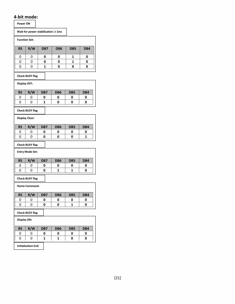
4-bit mode:
Initialization End
Display ON:
RS R/W DB7 DB6 DB5 DB4 0 0 0 0 0 0 0 0 1 1 X X
Check BUSY flag
Home Command:
RS R/W DB7 DB6 DB5 DB4 0 0 0 0 0 0 0 0 0 0 1 0
Check BUSY flag
Entry Mode Set:
RS R/W DB7 DB6 DB5 DB4 0 0 0 0 0 0 0 0 0 1 1 0
Check BUSY flag
Display Clear:
RS R/W DB7 DB6 DB5 DB4 0 0 0 0 0 0 0 0 0 0 0 1
Check BUSY flag
Display OFF:
RS R/W DB7 DB6 DB5 DB4 0 0 0 0 0 0 0 0 1 0 X X
Check BUSY flag
Function Set:
RS R/W DB7 DB6 DB5 DB4
0 0 0 0 1 0 0 0 0 0 1 0 0 0 1 0 X X
Wait for power stabilization: ≥ 1ms
Power ON
[22]
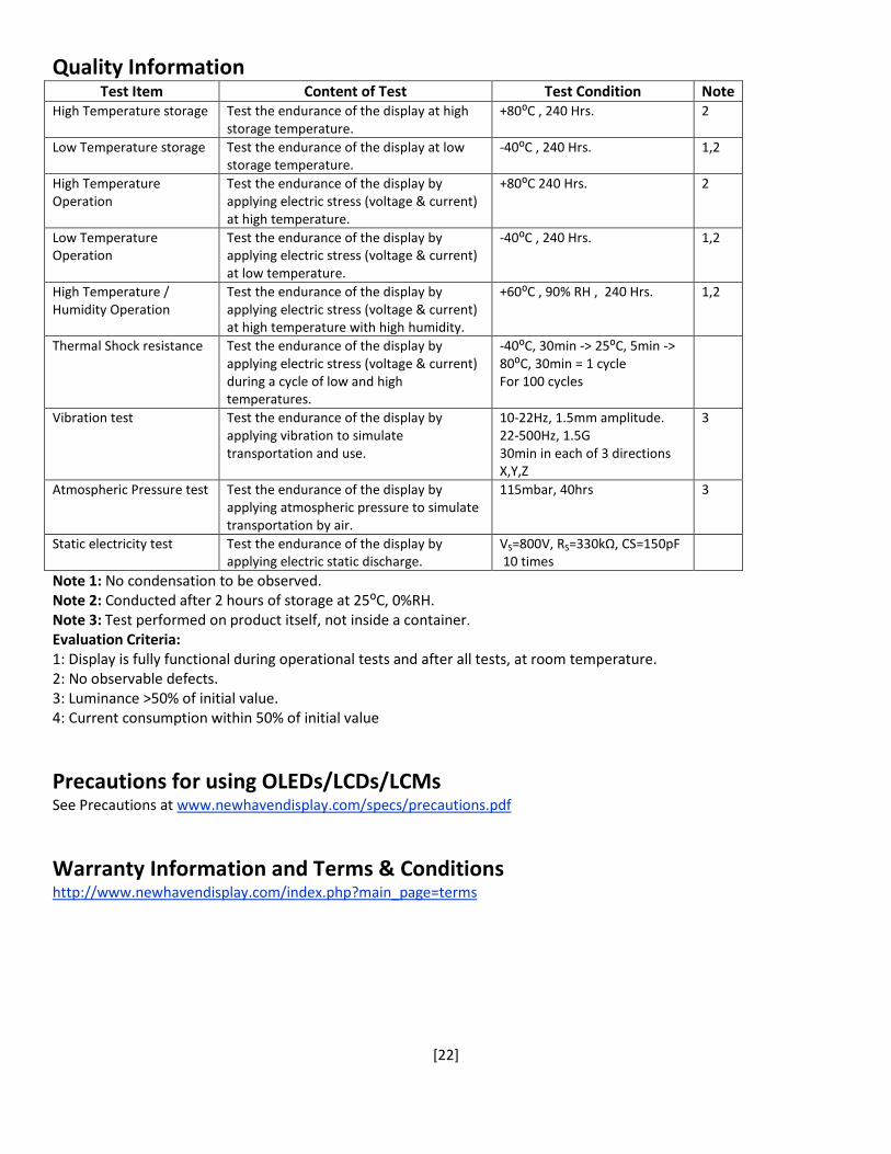
Quality Information Test Item Content of Test Test Condition Note
High Temperature storage Test the endurance of the display at high storage temperature.
+80⁰C , 240 Hrs. 2
Low Temperature storage Test the endurance of the display at low storage temperature.
-40⁰C , 240 Hrs. 1,2
High Temperature Operation
Test the endurance of the display by applying electric stress (voltage & current) at high temperature.
+80⁰C 240 Hrs. 2
Low Temperature Operation
Test the endurance of the display by applying electric stress (voltage & current) at low temperature.
-40⁰C , 240 Hrs. 1,2
High Temperature / Humidity Operation
Test the endurance of the display by applying electric stress (voltage & current) at high temperature with high humidity.
+60⁰C , 90% RH , 240 Hrs. 1,2
Thermal Shock resistance Test the endurance of the display by applying electric stress (voltage & current) during a cycle of low and high temperatures.
-40⁰C, 30min -> 25⁰C, 5min -> 80⁰C, 30min = 1 cycle For 100 cycles
Vibration test Test the endurance of the display by applying vibration to simulate transportation and use.
10-22Hz, 1.5mm amplitude. 22-500Hz, 1.5G 30min in each of 3 directions X,Y,Z
3
Atmospheric Pressure test Test the endurance of the display by applying atmospheric pressure to simulate transportation by air.
115mbar, 40hrs 3
Static electricity test Test the endurance of the display by applying electric static discharge.
VS=800V, RS=330kΩ, CS=150pF 10 times
Note 1: No condensation to be observed. Note 2: Conducted after 2 hours of storage at 25⁰C, 0%RH. Note 3: Test performed on product itself, not inside a container. Evaluation Criteria: 1: Display is fully functional during operational tests and after all tests, at room temperature. 2: No observable defects. 3: Luminance >50% of initial value. 4: Current consumption within 50% of initial value
Precautions for using OLEDs/LCDs/LCMs See Precautions at www.newhavendisplay.com/specs/precautions.pdf
Warranty Information and Terms & Conditions http://www.newhavendisplay.com/index.php?main_page=terms