new insights into organic light emitting devices ...397344/s4255954_final... · new insights into...
TRANSCRIPT
New Insights into Organic Light Emitting Devices:
photophysics, recombination, and out coupling
Fatemeh Pegah Maasoumi
A thesis submitted for the degree of Doctor of Philosophy at
The University of Queensland in 2016
School of Mathematics and Physics

I
Abstract
Display technology is expected to have a market industry value greater than 70 billion US
dollars by 2026. Although organic light emitting devices have found their way into the display
industry, there is still a need for higher device efficiencies, lower cost materials, and easier, scalable
production methods. This drives the need to gain a deeper understanding of organic
semiconductors, which can pave the way to these goals. As such, there is undeniable demand for
new classes of semiconductor materials, ideally with a high photoluminescence quantum yield,
balanced charge transport, and high light out-coupling through dipole engineering.
This thesis describes a body of work which specifically addresses the task of independent
control over luminescent, transport and processing properties of organic semiconducting materials
with dendritic structures. A family of Ir(III) complexes is introduced and studied including
dendrimers; poly(dendrimers); and co-polymers. In the first instance, photo-physical and electrical
properties of materials are described, before building on this knowledge to develop efficient organic
light emitting diodes. The dipole orientation was furthermore studied in these materials as an
intrinsic property of with a view to achieving higher out coupling. Finally, moving away from a
material-centric approaches and dendritic design, the charge transport and emissive properties of
organic semiconductors were simultaneously studied in a heterostructure light-emitting field effect
transistor by cryogenic techniques.
The main findings from this research were as follows: I) the photophysical properties
improved by increasing the number of dendron branches in the dendritic structure. This delivers
extra insulating space between the chromophore cores which leads to less concentration quenching;
II) combining dendrimers with a polymer backbone was beneficial not only toward improving the
film quality but also providing heteroleptic structures which are more likely to contain horizontally
oriented emissive dipoles; III) the results of temperature-dependent measurements demonstrated
that, as the device was cooled down, the intrinsic hole mobility followed an Arrhenius response
with the overall EQE increases.
The implications of these findings are toward simplifying the device structures using more
efficient devices. This can be achieved by means of highly luminescent materials as well as
enhancement in device out coupling, meaning that light can be emitted preferably perpendicular to
the device output plane. The fundamental studies also established some ground rules for
engineering high radiative efficiencies in light-emitting field effect transistors, which should aid in

II
both material and architecture design for future device iterations. Future work may concentrate on
chemically engineering the material structures for better properties as well as control over dipole
orientation.

III
Declaration by author
This thesis is composed of my original work, and contains no material previously published or
written by another person except where due reference has been made in the text. I have clearly
stated the contribution by others to jointly-authored works that I have included in my thesis.
I have clearly stated the contribution of others to my thesis as a whole, including statistical
assistance, survey design, data analysis, significant technical procedures, professional editorial
advice, and any other original research work used or reported in my thesis. The content of my thesis
is the result of work I have carried out since the commencement of my research higher degree
candidature and does not include a substantial part of work that has been submitted to qualify for
the award of any other degree or diploma in any university or other tertiary institution. I have
clearly stated which parts of my thesis, if any, have been submitted to qualify for another award.
I acknowledge that an electronic copy of my thesis must be lodged with the University Library and,
subject to the policy and procedures of The University of Queensland, the thesis be made available
for research and study in accordance with the Copyright Act 1968 unless a period of embargo has
been approved by the Dean of the Graduate School.
I acknowledge that copyright of all material contained in my thesis resides with the copyright
holder(s) of that material. Where appropriate I have obtained copyright permission from the
copyright holder to reproduce material in this thesis.
IV
Publications during candidature
Peer-reviewed journal articles
D. Gendron, E. Gann, K. Pattison, F. Maasoumi, C. E. McNeill, S. E. Watkins, P. L. Burn,
B. J. Powell and P. E. Shaw, “Synthesis and properties of pyrrolo[3,2-b]pyrrole-1,4-diones
(isoDPP) derivatives”, Journal of Materials Chemistry C, 2, 4276–4288, (2014).
F. Maasoumi, M. Ullah, P. E. Shaw, J. Li, P. L. Burn, P. Meredith and E. B. Namdas,
“Charge transport and recombination in heterostructure organic light emitting transistors”,
Organic Electronics, 25, 37-43, (2015).
K. Muhieddine, M. Ullah, F. Maasoumi, P. L. Burn and E. B. Namdas, “Hybrid Area
Emitting Transistors: Solution Processable and with High Aperture Ratios”, Advanced
Material, 27(42), 6677-6682, (2015).
A. Armin, P. Wolfer, P. E. Shaw, M. Hambsch, F. Maasoumi, M. Ullah, E. Gann, C. R.
McNeill, J. Li, Z. Shi, P. L. Burn and P. Meredith, “Simultaneous enhancement of charge
generation quantum yield and carrier transport in organic solar cells ”, Journal of
Materials Chemistry C, 3(41), 10799-10812, (2015).
M. Ullah, R. Wawrzinek, F. Maasoumi, S. C. Lo and E. B. Namdas, “Transparent and low
voltage operating organic light emitting transistors processed at low temperature ”,
Advanced Optical Materials, 3(0), 1-5, (2016).
Conference presentation
F. Maasoumi, M. Ullah, P. E. Shaw, J. Li, P. L. Burn, P. Meredith and E. B. Namdas,
“Charge transport and recombination in heterostructure organic light emitting transistors”,
Organic Field Effect Transistors XII, SPIE Optics and Photonics , San Diego USA, (2015),
poster presentation.
V
Publications included in this thesis
F. Maasoumi, M. Ullah, P. E. Shaw, J. Li, P. L. Burn, P. Meredith and E. B. Namdas,
“Charge transport and recombination in heterostructure organic light emitting transistors”,
Organic Electronics, 25, 37-43, (2015).
Incorporated as Chapter 6.
Contributor Statement of contribution
F. Maasoumi Designed experiments (80%)
Device fabrication (90%)
Paper writing (80%)
Paper editing (10%)
Dr M. Ullah Designed experiments (10%)
Device fabrication (10%)
Paper writing (10%)
Paper editing (15%)
Dr P. E. Shaw Photophysical characterisation (100%)
Paper writing (10%)
Paper editing (10%)
Dr J. Li Polymer synthesis (100%)
Paper editing (10%)
Prof. P. L. Burn Project supervision
Paper editing (15%)
Prof. P. Meredith Project supervision
Paper editing (20%)
Dr E. B. Namdas Project supervision
Designed experiments (10%)
Paper editing (20%)
VI
Contributions by others to the thesis
Chapter 3
The iridium dendrimer used for study was synthesised by Dr. Renji Wang. The ellipsometry
measurements were performed by Dr. Ravi Chandra Raju Nagiri on films that I prepared. The
photoelectron spectroscopy in air (PESA) measurements of ionization potential were performed by
Dr. Dani Stoltzfus at CSIRO in Clayton, Melbourne on films that I prepared.
Chapter 4
The dendrimer and poly(dendrimer) compounds were designed by Prof. Paul L. Burn and
synthesised by Dr. Ross D. Jansen-van Vuuren. The ellipsometry measurements were performed by
Dr. Ravi Chandra Raju Nagiri on films that I prepared. The photoelectron spectroscopy in air
(PESA) measurements of ionization potential were performed by Dr. Dani Stoltzfus at CSIRO in
Clayton, Melbourne on films that I prepared.
Chapter 5
The co-polymer dendrimers were designed by Prof. Paul L. Burn and synthesised by Dr. Ross D.
Jansen-van Vuuren. The photoelectron spectroscopy in air (PESA) measurements of ionization
potential were performed by Dr. Dani Stoltzfus at CSIRO in Clayton, Melbourne on films that I
prepared.
Chapter 6
The DPP-DTT polymer was synthesised by Dr. Jun Li from the institute of Material Research and
Engineering, Singapore. Dr. Mujeeb Ullah designed the asymmetric shadow masks. Dr. Ullah also
provided guidance and help in first device fabrication. The temperature dependent
photoluminescent measurement on Super Yellow was performed by Dr. Paul E. Shaw. The silicon
nitride substrates were diced by Khalid Muhieddine.
This thesis would not been possible without the collaboration with the CSIRO, Clayton, Melbourne.
Dr. Mark Bown, Dr. Chris Dunn and Dr. Jenny O’Connell who supervised the OLED device
fabrication and characterisation procedures carried out in the work described in this thesis.
VII
Statement of parts of the thesis submitted
to qualify for the award of another degree
None.

VIII
Acknowledgements
With these acknowledgements, I hope to do justice to the tremendous debt of gratitude I owe to
those who have supported me through love, friendship and intellect, and helped and inspired me to
be the researcher I am today.
To my mom, Zohreh Shahbazi, words are not enough for me to offer my affectionate gratitude for
your incredible dedication during my entire life. You are the one who planted the idea of being a
researcher by taking me as your companion on all your medical conferences. Distance may separate
us but I always feel like the luckiest girl to have you as my mom, my teacher, my best friend.
To Pouria, my lovely brother, I miss you to bits. I still can’t believe how hard it is to be so far from
my life shadow. It was you who took over my responsibilities back home so that I could pursue my
dreams. I owe you one. To John Lindorfer, my wonderful godfather, you filled my life not only
with your fatherly kindness and support but with all the experience, wisdom, and knowledge you
shared with me. You taught me to be a positive fighter just as you have been. A flash back to my
M.Phil, I would like to sincerely thank Prof. Alireza Bahrampour. It was you who encouraged me a
lot to pursue science. I wouldn’t be able to strive for my dreams here in the first place if it wasn’t
for your guidance and support.
To my PhD supervisors, Prof. Paul Meredith and Dr. Ebinazar Namdas. Paul, thank you so much
for taking me on as your student and also standing beside me for a long time to get me to Australia.
I am so grateful to have you not only as my supervisor but also as someone who listened to me and
helped me with my decisions. Ebinazar, thank you so much for always having your door open to
me, and being willing to discuss anything and everything that needed discussing. I really appreciate
your responsible and kind heart in supervision. To Prof. Paul Burn, thank you for profound insights
and guidance throughout my PhD. I am grateful to have worked with a pioneer in the field.
To Dr. Ardalan Armin, pal, what can I say, you were my mentor from the very first step in the lab.
To say that you provided me with the tools and support I needed. My eternal thanks to you for
teaching me so much of the science that I am pursuing now, giving me confidence and for
wonderful discussions we have had on just about every topic. To Dr. Mike Hambsch, thank you for
all of the scientific advice and thanks for taking me for running, cycling, hiking and all the fun
times we had together. You always talk me down from every ledge just like you were next to me,
even from the other side of the globe.
IX
Dr. Paul Shaw, it was with you and Dr. Mujeeb Ullah, that I have learned a great deal of
experimental skills. A special thanks to both of you for all of the training, help and fruitful
discussions. Dr. Andrew Clulow, many thanks for teaching me a lot more chemistry, English and
also beer brewing skills (I will attempt to do that sometime!).
To Khalid, my PhD buddy, we did it. My PhD journey was a lot easier with you making the bad
days seem not as bad. Thanks for showering me with your limitless kindness, support and 24/7
proofreading of whatever I wrote. Thanks for giving me heart even when you needed it most. To
Dr. Kristen Tandy, thanks for all the hugs and letters. You were such a lovely friend who supported
me in tough times when I needed it the most. Dr. Ross Van Vuuren, thank you so much for your
great materials, all the social activities and fruitful discussions. To Steven, you‘ve never hesitate to
help me with my urgent chemistry enquiries, thank you and good luck with your PhD.
I have to give a big thank you to the amazing scientists in CSIRO, Dr. Mark Bown, Dr. Chris Dunn,
and Dr. Jenny O’Connell. You came along just when I needed and are some of the most enthusiastic
and positive people I have ever met in science. I am so lucky to have had the opportunity to work
with you.
A substantial amount of thanks to Murray Kane and Stephanie Golding, SMP postgraduate
administrative officers and Rob Kembery, the business manager at COPE, for all of the help you
have provided me with and your immense patience. To Rob Webb and Helmut Land at the UQ
chemistry workshop, a special thanks to both of you for making and fixing all the precious
equipment.
To the wonderful crew at COPE, who helped me with bits and pieces in and out of the lab. In no
particular order: Helen, Vincent, Ravi, Robert, Soniya, Renji, Ajay, Fan, Ajeesh, Martin, Aren,
Larry, Kinitra. Thank you; I couldn’t ask for a better crowd to work with.
Last and not least, to the family I was privileged enough to choose.
Nahid and Mehdi, with you guys I feel loved, thanks for being my siblings away from home. To
continue on the note of feeling home, I must mention the wonderful Marianne and Luke. You took
so much care of me, without even asking or needing to be asked (especially at big T time). You are
my Australian family forever. To Safa, thanks for your sisterly love and support. To Sahar, thanks
for sending me positive energy. To the lovely couple, Nasim and Farid, thanks for your awesome
tea time company. To a special couple, Niloufar and Behnam thanks for the peaceful times you
gave me.
X
A special thanks to my amazing housemates, Shao, Swathi, Ely. Shao, thanks for your
thoughtfulness and for always being happy to help. It was nice to get out and talk about everything
other than work. Swathi, thanks for the love, support and for making me your delicious masala tea
every single morning. Ely, thanks for your excellent cheesecakes.
To Inna, thanks for the great time we had together. To Christian, you came along at the very end
and when I really needed someone to remind me of joy and laughter, thanks brownie. A great deal
of thanks to Saleh & Sima, Shahram, Pouria, Asha, Rob & Karrera, Michelle, Karyn, Julia. Thanks
for your company and fun time.
To my best friends, Marjon, Paria, Nazli, Aboozar, Speher, and Mehrsa your eternal friendship is
always a light to follow when the tunnels darken. You guys were believed in me even when I did
not. I love you all.
XI
Keywords
Organic semiconductors, light emitting, diodes, transistors, dendrimers, poly(dendrimers), iridium,
photo-physics
Australian and New Zealand Standard Research Classifications (ANZSRC)
ANZSRC code: 100702, Molecular and Organic Electronics, 50%
ANZSRC code: 03030, Optical Properties of Materials, 30%
ANZSRC code: 091208, Organic Semiconductors, 20%
Fields of Research (FoR) Classification
FoR code: 1007, Nanotechnology, 50%
FoR code: 0205, Optical Physics, 30%
FoR code: 0912, Material Engineering, 20%
XII
To Zohreh Shahbazi
My mom, My hero, My best friend….
XIII
Table of Contents
Abstract I
Declaration by author III
Publications during candidature IV
Contribution by others to the thesis VI
Acknowledgments VIII
Keywords and Classifications XI
Table of Contents XIII
List of Figures XVI
List of Tables XXII
List of Abbreviations and Symbols XXIII
Chapter 1: Introduction 1
1.1 Motivation 1
1.2 Properties of organic semiconductors 3
1.2.1 Energy levels and nomenclature 4
1.3 Dendrimers 5
1.4 Luminescence and electroluminescence 6
1.5. Organic light emitting diodes 8
1.5.1 Operating mechanism, parameters, and performance metrics 8
1.5.2 Loss mechanism and dipole orientation in OLEDs 11
1.6 Organic light emitting field effect trabsistors 15
1.6.1 Operating mechanism, parameters and performance metrics 15
1.6.2 Temperature-dependent measurements 18
1.7 Aims of this project 20
References 22
Chapter 2 : Experimental Methods and Equipment 28
2.1 Introduction 28
2.2 Materials 28
2.3 Material characteristics 29
2.3.1 Energy level eastimation 29
2.3.2 Absorption 29
XIV
2.3.3 Photoluminensce 29
2.3.4 Photoluminescence quantum yield 30
2.3.5 Photoluminescence decay lifetime 32
2.3.6 Ellipsometry 33
2.3.7 Dipole orientation measurement 33
2.4 Device fabrication 35
2.4.1 Substrate preparation 36
2.4.2 Thin film deposition 36
2.4.3 Film thickness determination 36
2.4.4 Contact deposition 37
2.5 Device characterisation 37
2.5.1 Standard measurements for light emission 37
2.5.2 Colourimetry 40
2.5.3 Standard OLED characterisation 42
2.5.4 Standard LEFET characterisation 43
2.5.4.1 Optical characterisation 43
2.5.4.2 Electrical characterisation 44
References 46
Chapter 3: Highly Efficient Solution-Processable Dendrimer OLEDs 47
3.1 Introduction 47
3.2 Material design and experimental methods 48
3.3 Photo-physical properties 50
3.4 Device performance 52
3.5 Dipole orientation 56
3.6 Conclusion 59
References 60
Chapter 4 : Effects of Polymerisation and Dendronisation on iridium (III) OLEDs 62
4.1 Introduction 62
4.2 Singly-dendronised dendrimer and poly(dendrimer) 63
4.2.1 Material design and experimental methods 63
4.2.2 Photo-physical properties 65
4.2.3 Device performance 69
XV
4.2.4 Dipole orientation 73
4.3 Doubly-dendronised dendrimer and poly(dendrimer) 75
4.3.1 Material design and experimental methods 75
4.3.2 Photo-physical properties 77
4.3.3 Device performance 80
4.4 Conclusion 84
References 86
Chapter 5 : Ambipolar Poly(dendrimers) 88
5.1 Introduction 88
5.2 Material design and experimental methods 89
5.3 Photo-physical properties 91
5.4 Device performance 94
5.5 Conclusion 98
References 99
Chapter 6 : Charge Transport and Recombination in Heterostructure Organic Light
Emitting Transistors
100
6.1 Introduction 100
6.2 Experimental procedure 101
6.2.1 Device fabrication 101
6.2.2 Temperature dependent measurement 103
6.2.3 Photoluminescence quantum yield measurement 105
6.3 Results and discussions 105
6.3.1 Room temperature 105
6.3.2 Variable temperature mobility measurements 108
6.3.3 Variable temperature radiative recombination efficiency 112
6.4 Conclusion 114
References 115
Chapter 7 : Summary, Conclusion, and Outlook 118
Appendix 122
XVI
List of Figures
1.1 A next generation iWatch, which will have a 1.3-1.5 inch flexible OLED-display…………...…2
1.2 a) Figure 1.2 a) The bonding system of ethene showing the σ- and π-bonds, b) the corresponding
energy level diagram of ethene. The lowest energy electronic excitation shown is between the
bonding π-orbital and the antibonding π*-orbital, adapted from………………………………...4
1.3 A schematic diagram of the first generation of a dendritic structure consisting of a core,
branching units and surface groups………………………………………………………………5
1.4 A Jablonski diagram illustrating the possible relaxation pathways in the singlet and triplet
manifolds…………………………………………………………………………………………7
1.5 OLED device structure, a) an OLED comprising a single active layer, b) a schematic
mechanism of OLED operation illustrating the basic processes of electroluminescence. Holes
are injected from the anode into the HOMO of the hole injection layer and pass to the hole
transport layer. Electrons are injected from the cathode into the LUMO of the electron injection
layer EIL and pass to the electron transport layer. Excitons are formed in the emissive layer and
emission will occur, c) a multilayer OLED……………………………………………………....9
1.6 a) Schematic illustration of loss mechanisms in an OLED. With no out-coupling enhancement
only a small amount of emission escapes to be observed, b) the distribution of different optical
losses for a comparable fluorescent or phosphorescent emitters with similar stack layer
thickness, refractive indices and emission spectra…………………………………………...…12
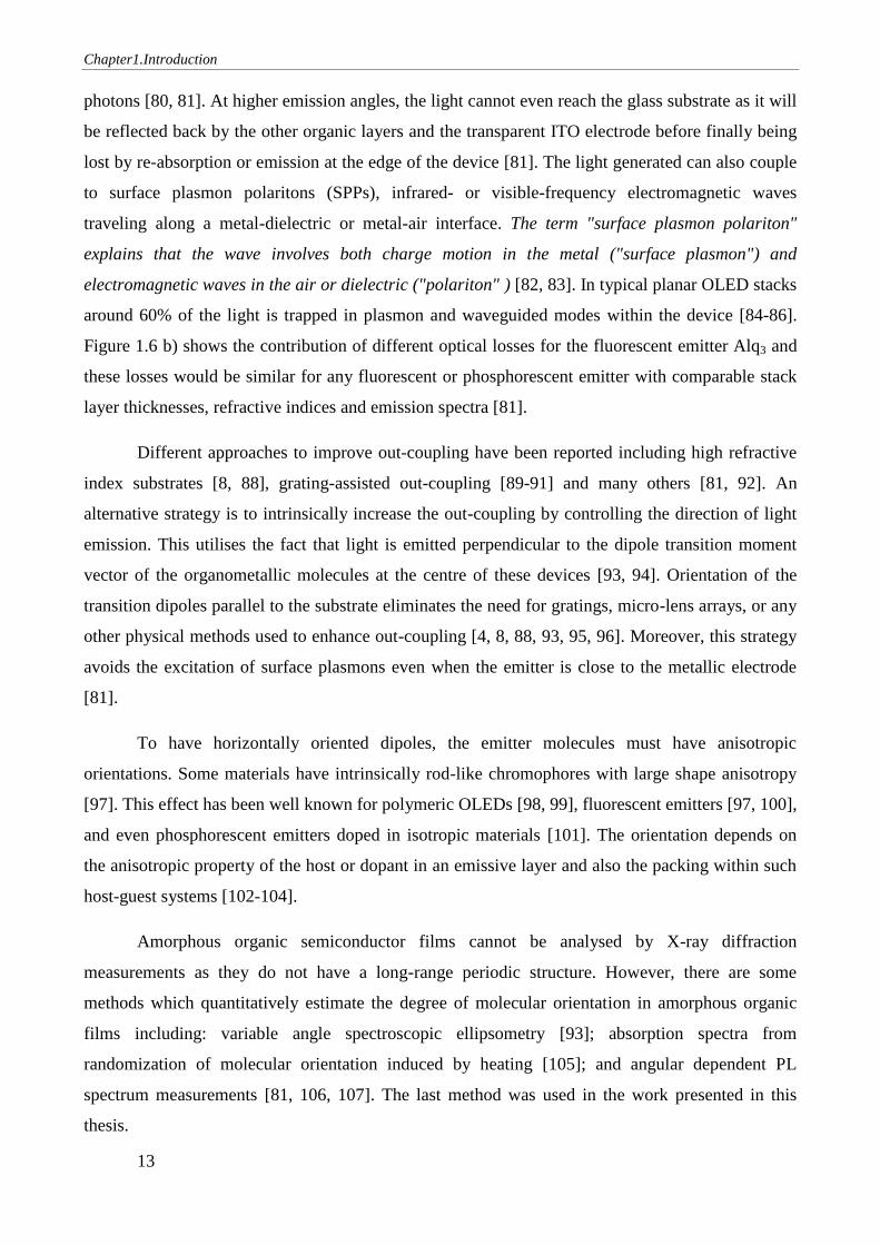
1.7 a) The conventional definition for dipole orientation, b) A cross-sectional schematic view of the
angular dependent PL spectrum set up , c) A schematic diagram of the experimental setup with
angle notations and emission polarizer orientations for recording s- and p- polarized emission,
adapted from…………………………………………………………………………………….14
1.8 Schematic diagrams including the p-type operating mechanisms of a) a single layer LEFET and
b) a multi-layer LEFET………………………………………………………………………...16
1.9 a) Transfer characteristics of a n-type LEFET showing the source-drain current (IDS) as a
function of the applied gate voltage (VG) with a fixed source-drain voltage (VDS). b) The
output characteristics of the LEFET showing the IDS as a function of VDS for different values
of VG……………………………………………………………………………………………18
XVII
1.10 A schematic of the Multiple Trapping and Release Model adopted from……..……………19
2.1 Schematic diagram of the experimental set up of PLQY measurement of organic thin films….30
2.2 Relationship between the optical anisotropy in films and molecular orientation………………34
2.3 Close up of the angle dependent PL spectrum setup from two directions……………………...35
2.4 Schematic device structure for OLED and LEFET……………………………………………..36
2.5 Normalized CIE 1931 eye response curve as a function of wavelength………………………..38
2.6 a) CIE 1931 colour-matching functions , , and which represent red, green , blue
light respectively as a function of wavelength, note that the green colour-matching function , is
identical to the eye response curve. b) chromaticity diagram representing the possible colours the
human eye can perceive with and co-ordinates …………………………………………….…41
2.7 Two photographs showing the experimental set-up for OLED testing utilised at the CSIRO test
facility……………………………………………………………………………………………….42
2.8 Photographs showing the experimental setup for LEFET testing utilised at the COPE test
facility………………………………………………………………………………………………44
3.1 The chemical structures of a) G1 Ir(ppy)3, b) CBP, and c) TPBi………………………………48
3.2 a) Device structure, b) energy diagram for different layers. The HOMO and LUMO of TPBi and
CBP were taken from literature respectively. The work function for metals were taken from original
material sheets provided by CSIRO, the energy level of G1 Ir(ppy)3 were obtained from PESA
measurements as explained in Chapter 2…………………………………………………………....49
3.1 Absorption and PL spectrum for G1 Ir(ppy)3 in solution (solid line), in neat film (dash line), and
in CBP blend film (dot line), the samples were excited at a wavelength of325 nm for PL
measurements……………………………………………………………………………………….51
3.4 Photoluminescence lifetime measurement (TCSPC) for G1 Ir(ppy)3 in a degassed solution
(square), in neat film (circle), and in CBP blend (star). The samples were excited by a 372 nm LED
and the emission was detected at 515 nm (peak)…………………………………………………...51
3.5 Current density and luminance characteristics for neat and CBP blend devices. The square
represents the neat films while the circle represents the blends. Open grey colour show current
density and solid black colour represents the luminance…………………………………….……..53
3.6 a) EL spectrum for neat and CBP blend devices, b) a close up of the working device, c) the
overlapped CIE co-ordinates of both devices………………………………………………….……54
XVIII
3.7 EQE values for neat and CBP blend devices……………………………………………………54
3.8 Power efficiency for both neat and CBP blend devices………………………………………...55
3.2 Refractive index and extinction coefficient for neat (dot line) and CBP blend (solid line) of G1
Ir(ppy)3……………………………………………………………………………………………...57
3.10 Experimental data (circles) and fitting (dash line) for angle dependent PL spectrum
measurement………………………………………………………………………………………...58
3.3 Refractive index and extinction coefficient for PEDOT:PSS…………………………………..58
4.1 Chemical structures of, a) singly-dendronised dendrimers D1 and, b) singly-dendronised poly
(denrimers) P1, with M̅w of 160 kDa and a polydispersity (PDI) of 1.3…………………………...64
4.2 a) Device structure, b) energy level diagram for different layers……………………………….65
4.1 Normalized absorption (black) and PL (blue) spectra of singly-dendronised dendrimers D1 and
poly (dendrimers) P1 for solution (solid line), neat film (dash line), and CBP blend film (dotted
line)………………………………………………………………………………………………….66
4.4 Lifetime measurements (TCSPC) for: a) singly-dendronised dendrimer (D1) and b)
poly(dendrimers) (P1) in degassed solution, neat film, and CBP blend film. Comparing the solid
state neat film of both compounds, it can be noted that the bi-exponential PL decay moving toward
the mono-exponential decay. The samples were excited by a 372 nm LED and the emission was
detected at the peak of PL spectra (520nm- 525nm)………………………………………………..67
4. 5 Current density and luminance characteristics in neat (square) and CBP blend (circle) devices
for singly-dendronised: a) dendrimer (D1), and b) poly (dendrimers) (P1)………………………..70
4.7 Efficiency of devices are presented for both compounds in different units: a) EQE and b) power
efficiency (left axis) and luminous efficiency (right axis)………………………………………….72
4.2 Variable angle spectroscopic ellipsometry (a and c) and angle dependent PL results (b and d)
for singly-dendronised compounds D1 and P1 respectively……………………………………….74
4.3 Chemical structures of, a) doubly-dendronised dendrimer, D2, b) doubly-dendronised
poly(dendrimer), P2 with a M̅w of 68 kDa and a PDI of 2.4……………………………………..…76
4.4 Energy level diagram for doubly-dendronised compounds……………………………………..76
4.5 Normalized absorption (black) and PL (blue) spectra for doubly-dendronised dendrimer, D2,
and poly(dendrimer), P2, for solution (solid line), neat film (dash line), CBP blend film (dotted
XIX
line), PL absorption of singly-dendronised compounds are also plotted in orange dash line for
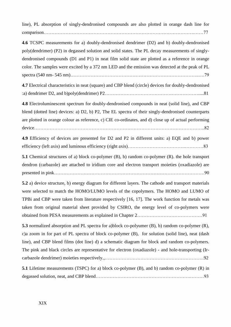
comparison…………………………………………………………………………………….……77
4.6 TCSPC measurements for a) doubly-dendronised dendrimer (D2) and b) doubly-dendronised
poly(dendrimer) (P2) in degassed solution and solid states. The PL decay measurements of singly-
dendronised compounds (D1 and P1) in neat film solid state are plotted as a reference in orange
color. The samples were excited by a 372 nm LED and the emission was detected at the peak of PL
spectra (540 nm- 545 nm)………………………………………………………………………..….79
4.7 Electrical characteristics in neat (square) and CBP blend (circle) devices for doubly-dendronised
:a) dendrimer D2, and b)poly(dendrimer) P2…………………………………………………….....81
4.8 Electroluminescent spectrum for doubly-dendronised compounds in neat (solid line), and CBP
blend (dotted line) devices: a) D2, b) P2, The EL spectra of their singly-dendronised counterparts
are plotted in orange colour as reference, c) CIE co-ordinates, and d) close up of actual performing
device………………………………………………………………………………………………..82
4.9 Efficiency of devices are presented for D2 and P2 in different units: a) EQE and b) power
efficiency (left axis) and luminous efficiency (right axis)……………………………….…………83
5.1 Chemical structures of a) block co-polymer (B), b) random co-polymer (R). the hole transport
dendron (carbazole) are attached to iridium core and electron transport moieties (oxadiazole) are
presented in pink…………………………………………………………………………………….90
5.2 a) device structure, b) energy diagram for different layers. The cathode and transport materials
were selected to match the HOMO/LUMO levels of the copolymers. The HOMO and LUMO of
TPBi and CBP were taken from literature respectively [16, 17]. The work function for metals was
taken from original material sheet provided by CSIRO, the energy level of co-polymers were
obtained from PESA measurements as explained in Chapter 2……………………………………91
5.3 normalized absorption and PL spectra for a)block co-polyumer (B), b) random co-polymer (R),
c)a zoom in for part of PL spectra of block co-polymer (B), for solution (solid line), neat (dash
line), and CBP blend films (dot line) d) a schematic diagram for block and random co-polymers.
The pink and black circles are representative for electron (oxadiazole) - and hole-transporting (Ir-
carbazole dendrimer) moieties respectively.,……………………………………………………….92
5.1 Lifetime measurements (TSPC) for a) block co-polymer (B), and b) random co-polymer (R) in
degassed solution, neat, and CBP blend…………………………………………………….………93
XX
5.5 Current density and luminance characteristics for a) block co-polymer (B) with separate
distribution of electron- and hole-transporting moieties, b) random co-polymer (R) with random
distribution of oxadiazole group to polymer back bone………………………………………….....95
5.2 a) Electroluminescent for three compounds in blends, b) CIE co-ordinates for both co-
polymers…………………………………………………………………………………………….96
5.7 a) EQE values for block co-polymer (square) and random co-polymer (circle) in neat (black
colour) and blend (grey colour), b) power efficiency and luminous efficiency for both compounds97
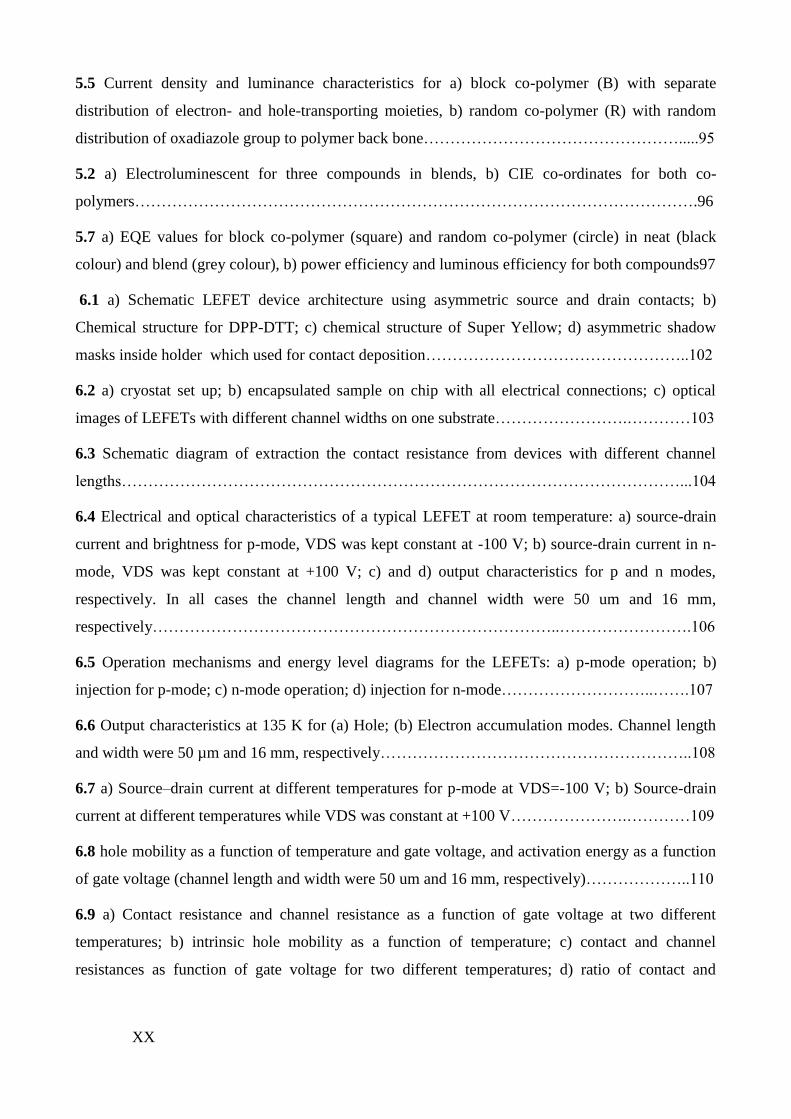
6.1 a) Schematic LEFET device architecture using asymmetric source and drain contacts; b)
Chemical structure for DPP-DTT; c) chemical structure of Super Yellow; d) asymmetric shadow
masks inside holder which used for contact deposition…………………………………………..102
6.2 a) cryostat set up; b) encapsulated sample on chip with all electrical connections; c) optical
images of LEFETs with different channel widths on one substrate…………………….…………103
6.3 Schematic diagram of extraction the contact resistance from devices with different channel
lengths……………………………………………………………………………………………...104
6.4 Electrical and optical characteristics of a typical LEFET at room temperature: a) source-drain
current and brightness for p-mode, VDS was kept constant at -100 V; b) source-drain current in n-
mode, VDS was kept constant at +100 V; c) and d) output characteristics for p and n modes,
respectively. In all cases the channel length and channel width were 50 um and 16 mm,
respectively…………………………………………………………………..…………………….106
6.5 Operation mechanisms and energy level diagrams for the LEFETs: a) p-mode operation; b)
injection for p-mode; c) n-mode operation; d) injection for n-mode………………………..…….107
6.6 Output characteristics at 135 K for (a) Hole; (b) Electron accumulation modes. Channel length
and width were 50 µm and 16 mm, respectively…………………………………………………..108
6.7 a) Source–drain current at different temperatures for p-mode at VDS=-100 V; b) Source-drain
current at different temperatures while VDS was constant at +100 V………………….…………109
6.8 hole mobility as a function of temperature and gate voltage, and activation energy as a function
of gate voltage (channel length and width were 50 um and 16 mm, respectively)………………..110
6.9 a) Contact resistance and channel resistance as a function of gate voltage at two different
temperatures; b) intrinsic hole mobility as a function of temperature; c) contact and channel
resistances as function of gate voltage for two different temperatures; d) ratio of contact and
XXI
channel resistances for different gate voltages and temperatures. All plots are for electron
accumulation mode. In all cases channel length and width were 50 µm and 16 mm, respectively.111
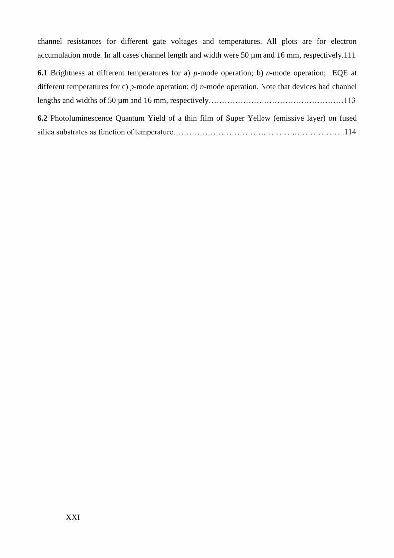
6.1 Brightness at different temperatures for a) p-mode operation; b) n-mode operation; EQE at
different temperatures for c) p-mode operation; d) n-mode operation. Note that devices had channel
lengths and widths of 50 µm and 16 mm, respectively……………………………………………113
6.2 Photoluminescence Quantum Yield of a thin film of Super Yellow (emissive layer) on fused
silica substrates as function of temperature……………………………………….……………….114
XXII
List of Tables
3.1 Summary of PLQY and PL decay values for G1 Ir(ppy)3 in solution, neat film, and CBP
blend………………………………………………………………………………………………...52
3.2 A summary of device performance parameters for neat and CBP blend emissive layers……....56
4.1 A summary of PLQY and PL decay values for singly-dendronised compounds in degassed
solution, solid state neat and, blend…………………………………………………………………68
4.2 A summary of electrical characterization and out-coupling calculations for carbazole dendrimers
and poly (dendrimers) in neat and blended devices……………………………………………...…73
4.3 A summary of PLQY and PL decay values for doubly-dendronised compounds in degassed
solution and solid states……………………………………………………………………………..78
4.4 A summary of electrical characterization and outcoupling calculations from doubly-dendronised
dendrimer and poly(dendrimer) in devices…………………………………………….……………84
5.1 A summary of the photo-physical characteristics for the co-polymer family in solution, neat
films, and CBP blends………………………………………………………..……………………..94
5.2 A summary of device performance (left side) and out-coupling values (right side) for devices of
both compounds……………………………………………………………………………………..98
XXIII
List of Abbreviations and Symbols
Si Silicon
Ge Germanium
CRT Cathode ray tube
FPD Flat panel display
LCD Liquid crystal display
LED Light emitting diode
FET Field effect transistor
LEFET Light emitting field effect transistor
IP Ionisation potential
EA Electron affinity
HOMO Highest occupied molecular orbital
LUMO Lowest unoccupied molecular orbital
k Total decay rate
kR Radiative decay rate
kNR Non-radiative decay rate
I(t) Time resolved photoluminescence intensity
I0 Initial luminescence
EML Emissive layer
A+
Hole (cation)
A-
Electron (anion)
A0 Ground state
A*
Product of Coulombically bound electron and hole
HTM Hole-transporting material
ETM Electron-transporting material
HTL Hole-transporting layer
ETL Electron-transporting layer
EQE External quantum efficiency
CIE Commission Internationale de I’Eclairage
NTSC National television standard committee
HIL Hole injection layer
EIL Electron injection layer
HBL Hole blocking layer
XXIV
EBL Electron blocking layer
HIM Hole injection material
EIM Electron injection material
PEDOT Poly(3,4-ethylenedioxythiphene)
ϕEQE External quantum efficiency
ϕescape Amount of generated photons escaping from the device
ϕcapture Fraction of electrons and holes that recombine to form excitons
ϕspin Spin statistics
ϕPLQY Photoluminescence quantum yield
ITO Indium tin oxide
SPP Surface plasmon polariton
px Dipole in x axis
py Dipole in y axis
pz Dipole in z axis
OFET Organic field-effect transistor
L Channel length
W Channel width
VG Gate voltage
VDS Source-drain voltage
IDS Source-drain current
µ Mobility
c Dielectric capacitance
Vt Threshold voltage
µD Drift mobility
µ0 Trap free mobility
Et Activation energy
KB Boltzmann’s constant
T Temperature
PLQY Photoluminescence quantum yield
COPE Centre for organic photonics and electronics
DPP-DTT Diketopyrrolopyrrole–dithienothiophene
CBP 4,4’-N,N’-dicarbazolyl-biphenyl
TPBi 2,2',2"-(1,3,5-Benzinetriyl)-tris(1-phenyl-1-H-benzimidazole)
SY phenyl-substituted poly(p-phenylenevinylene), super yellow
PL Photoluminensce
A Absorbance
XXV
PMT Photomultiplier tube
QS PLQY value of sample
QR PLQY value for reference
AS Absorbance of sample
AR Absorbance of reference
nS Refractive index of sample
nR Refractive index of reference
DS Sums of corrected photoluminensce for sample
DR Sums of corrected photoluminensce for reference
Xlaser Intensity of the excitation laser
Xsample Intensity of total emission from sample
Xsphere Photodiode intensity for integrated sphere
R Reflected excitation power
ƞ PLQY value
TCSPC Time correlated single photon counting
VASE Variable angle spectroscopic ellipsometry
S Orientation order parameter
Ke Extraordinary extinction coefficient
Ko Ordinary extinction coefficient
TM Transverse magnetic
PEDOT:PSS Poly(3,4-ethylenedioxythiophene) polystyrene sulfonate
𝜙𝑙𝑢𝑚 Luminous flux
EL(λ) Radiation intensity
ER(λ) Eye response
Pout Optical power
nph Number of photons
ne Number of electrons
X Tristimulus x value
Y Tristimulus y value
Z Tristimulus z value
x(λ) Colour matching function representing red light
y(λ) Colour matching function representing green light
z(λ) Colour matching function representing blue light
J Current density
Ƞ*
Power efficiency
MLCT Metal to ligand charge transfer
XXVI
EL Electroluminescence
ROMP Ring opening metathesis polymerisation
SCLC Space charge limited current
Photo-CELIV Photo-charge extraction in linearly increasing voltage
LPCVD Low pressure physical vapor deposition
PMMA Poly (methylmethacrylate)
Rt Total resistance
Rch Channel resistance
Rc Contact resistance
1
Chapter 1
Introduction
1.1 Motivation
Over the last seventy years, an inorganic family of semiconductors, mainly consisting of
silicon (Si) and germanium (Ge) has revolutionized all aspects of our lives through electronics.
Products of a multi-billion US dollar industry have filled our everyday life: from personal mobile
phones and computers, to satellites, solar energy panels, and the worldwide internet. A key part of
this industry is transmitting the electronic information to human visual understanding through
“display technology”. This sector of technology is likely to be the most rapidly expanding market in
coming years as it has so many use in different electronic devices [1].
Cathode ray tube (CRT) displays dominated the market for a long time and employ the
thermionic emission principle, which required use of high voltages and vacuum. CRT displays were
therefore heavy and bulky because of weight and size of the required components. In spite of a
number of effective and innovative changes in CRTs, they have been replaced by flat-panel displays
(FPDs) such as liquid crystal displays (LCDs) and plasma displays. Plasma displays on the other
hand provide high quality pictures over wide viewing angles. However in comparison with CRT
and LCD displays they have shorter display lifetimes [2].
Light emitting diodes (LEDs) are another member of the flat-panel display family, which
operate by direct conversion of electrical energy to visible light in semiconductors. LEDs normally
have long operational lifetimes due to utilising solid state semiconductors, which are
electrochemically more stable.
Lately, more research has focused on LEDs manufactured from organic semiconductors
called OLEDs. Organic semiconductors exhibit many novel physical, electrical and optical
properties. These properties include the potential for large-area solution processing, compact size of
the functional layers, flexibility, and almost unlimited possibilities with respect to molecular design,
that are not typically available to conventional inorganic semiconductors (e.g Ge, Si). These novel
properties of organic semiconductors have generated new opportunities not only for display
technology but solar cells, sensors, detectors, and field effect transistors (FETs).
Chapter1.Introduction
2
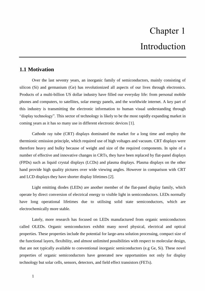
Figure 1.1 A next generation iWatch, which will have a 1.3-1.5 inch flexible OLED-display [3]
OLEDs provide colour vibrancy, high colour contrast ratio, excellent power efficiency and a
range of fabrication conditions making them suitable for flexible substrates, ultrathin displays, and
smartphones (see Figure 1.1) [4-6]. Beyond these applications, white light emitting OLEDs are
attracting attention in the lighting market due to their higher efficiency and performance in
comparison with their inorganic counterparts and fluorescent tubes [7, 8], and new product design
and lighting opportunities due to the unique processability of organic semiconductors [9].
OLED displays still require transistor-based backplane circuits to switch their elements. The
cost of this FET panel circuitry is more expensive than the OLED itself. However, The
electroluminescence properties of OLEDs can be combined with the switching properties of
transistors in a single architecture to produce a class of devices called light emitting field effect
transistors (LEFETs) [10]. The dual functionality of LEFETs provides the potential for new
applications such as simplified pixels for flat panel displays [11], LEFETs can tolerate higher
current densities than OLEDs and also in some cases can transfer the emission zone from
underneath the metal electrodes [12, 13]. Furthermore, LEFETs are convenient tools for studying
fundamental charge transport and photo-physical processes in organic semiconducting materials and
this will be explored in the work presented in this thesis.
Although remarkable steps have so far been taken towards understanding the behaviour of
organic semiconductors, a number of fundamental issues remain unknown. Also, some additional
device and manufacturing related challenges are: avoiding complex device structure with more than
Chapter1.Introduction
3
three layers; solution processibility; host free materials with high photoluminescence suitable for
single layer devices; low operation voltage; and increasing out-coupling using novel concepts such
as molecular alignment. Therefore, progress in the OLED industry demands new material
developments and device architectures with promising photo-physical and electrical properties.
However, controlling the charge transport and emissive properties of OLED materials remains a key
research area due to the complicated nature of their disordered structure, which also can be affected
by processing condition [14-22]. All of these considerations motivated the work that is described in
this thesis, which focuses on the understanding of phosphorescent OLED materials.
1.2 Properties of organic semiconductors
Organic semiconductors are based on carbon chains. Isolated carbon atoms have a ground
state electronic configuration of 1s22s
22p
2 and they can act as conductive materials through orbital
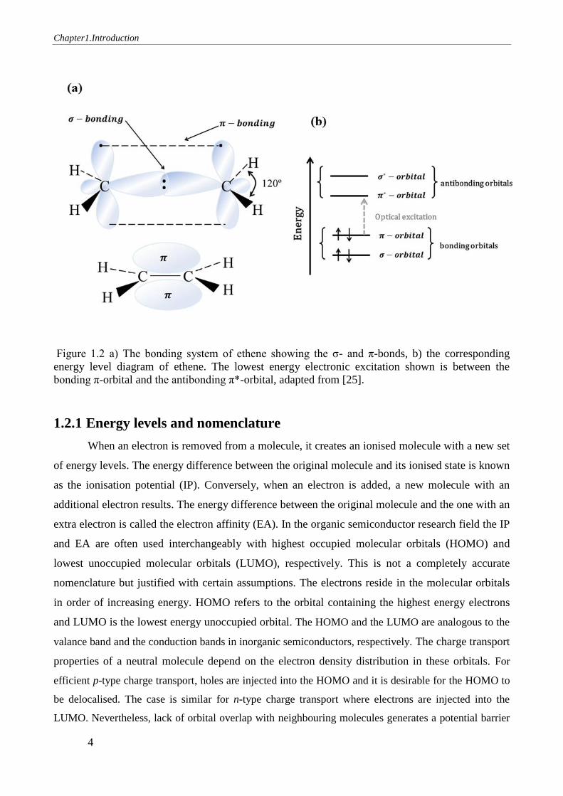
hybridisation in the bonding configuration. Organic semiconductors have a conjugated 𝜋-electron
system formed by overlapping P orbitals of sp2-hybridised carbon atoms within the molecules [23].
In this configuration each carbon atom has three sp2 orbitals, two bonded to the neighbouring
carbon atoms in the carbon chain and the third to a hydrogen atom or another carbon atom. The
fourth valence electron resides in a p-orbital and may become delocalised along the carbon chain by
overlap of p-orbitals to form a chain of π-orbitals. The p-orbitals can overlap either in phase or out
of phase to form bonding (π) or antibonding (π*) molecular orbitals respectively [24]. The 𝜋-
bonding is weaker than the σ-bonding framework forming the backbone of the molecule due to
poorer orbital overlap. Therefore, the π-π* transitions in conjugated molecules are typically the
lowest energy electronic excitation with energy gaps of between 1.5 and 3 eV. This allows
absorption and emission of light in the visible spectral range (see Figure 1.2) and the energy gap can
be controlled by the degree of conjugation in the organic semiconductor. Therefore the
optoelectronic properties can be tuned by molecular engineering [25].
Chapter1.Introduction
4
Figure 1.2 a) The bonding system of ethene showing the σ- and π-bonds, b) the corresponding
energy level diagram of ethene. The lowest energy electronic excitation shown is between the
bonding π-orbital and the antibonding π*-orbital, adapted from [25].
1.2.1 Energy levels and nomenclature
When an electron is removed from a molecule, it creates an ionised molecule with a new set
of energy levels. The energy difference between the original molecule and its ionised state is known
as the ionisation potential (IP). Conversely, when an electron is added, a new molecule with an
additional electron results. The energy difference between the original molecule and the one with an
extra electron is called the electron affinity (EA). In the organic semiconductor research field the IP
and EA are often used interchangeably with highest occupied molecular orbitals (HOMO) and
lowest unoccupied molecular orbitals (LUMO), respectively. This is not a completely accurate
nomenclature but justified with certain assumptions. The electrons reside in the molecular orbitals
in order of increasing energy. HOMO refers to the orbital containing the highest energy electrons
and LUMO is the lowest energy unoccupied orbital. The HOMO and the LUMO are analogous to the
valance band and the conduction bands in inorganic semiconductors, respectively. The charge transport
properties of a neutral molecule depend on the electron density distribution in these orbitals. For
efficient p-type charge transport, holes are injected into the HOMO and it is desirable for the HOMO to
be delocalised. The case is similar for n-type charge transport where electrons are injected into the
LUMO. Nevertheless, lack of orbital overlap with neighbouring molecules generates a potential barrier
Chapter1.Introduction
5
between molecules, which leads to charge carriers being trapped on a molecule and poorer charge
transport overall.
1.3 Dendrimers
Traditionally, organic semiconductors have been divided to the two main classes of small
molecules and polymers. Small molecules are attractive due to their simple, well-defined molecular
structure and their mono-dispersity. However, not all of them are soluble and are typically deposited
through high vacuum and thermal evaporation techniques [26-30]. On the other hand, polymers are
generally processed from solution via spin-coating and inkjet printing. This is a promising feature
for fast, large area, and low temperature mass production in display technology. Although solution
processing of polymers is less wasteful than evaporation with patterning, the reproducibility of
polymer synthesis in terms of the polydispersity (a measure of the distribution of molecular mass in
a given polymer sample), molecular weight, and backbone defects is difficult to control [31-34].
The work presented in this thesis is mainly focused on an emerging class of organic
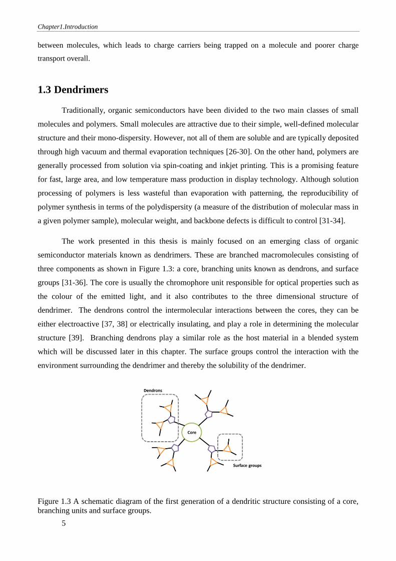
semiconductor materials known as dendrimers. These are branched macromolecules consisting of
three components as shown in Figure 1.3: a core, branching units known as dendrons, and surface
groups [31-36]. The core is usually the chromophore unit responsible for optical properties such as
the colour of the emitted light, and it also contributes to the three dimensional structure of
dendrimer. The dendrons control the intermolecular interactions between the cores, they can be
either electroactive [37, 38] or electrically insulating, and play a role in determining the molecular
structure [39]. Branching dendrons play a similar role as the host material in a blended system
which will be discussed later in this chapter. The surface groups control the interaction with the
environment surrounding the dendrimer and thereby the solubility of the dendrimer.
Figure 1.3 A schematic diagram of the first generation of a dendritic structure consisting of a core,
branching units and surface groups.
Chapter1.Introduction
6
A particular advantage of dendrimer molecules is that the dendron and the core can be made
electrically independent, meaning that the type of dendron attached to the core will have no effect
on the electronic properties of the core. Consequently, the electronic properties of dendrimers can
be defined in three different ways by dendrons [40]; the type and the number of the dendrons
attached; and the number of branching levels from the core known as the dendrimer generation.
Therefore, careful dendrimer design of the dendrons can yield efficient charge transport with no
influence on the other properties such as emission colour and solubility [21, 41]. Dendrimers can
therefore be designed to be ink-jet or screen printed by choosing appropriate surface groups [42].
Dendrimers are seen as promising candidates for OLED technology as they incorporate the
advantages of small molecules and conjugated polymers. A new promising approach for OLED
materials are poly(dendrimer)s. Polymers with pendant side-chain chromophore cores encapsulated
by dendrons, which combine the advantages of dendrimers in reducing the quenching of the emitter
with the viscosities of polymers.
1.4 Luminescence and electroluminescence
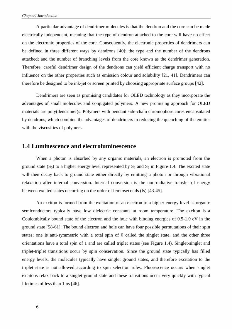
When a photon is absorbed by any organic materials, an electron is promoted from the
ground state (S0) to a higher energy level represented by S1 and S2 in Figure 1.4. The excited state
will then decay back to ground state either directly by emitting a photon or through vibrational
relaxation after internal conversion. Internal conversion is the non-radiative transfer of energy
between excited states occurring on the order of femtoseconds (fs) [43-45].
An exciton is formed from the excitation of an electron to a higher energy level as organic
semiconductors typically have low dielectric constants at room temperature. The exciton is a
Coulombically bound state of the electron and the hole with binding energies of 0.5-1.0 eV in the
ground state [58-61]. The bound electron and hole can have four possible permutations of their spin
states; one is anti-symmetric with a total spin of 0 called the singlet state, and the other three
orientations have a total spin of 1 and are called triplet states (see Figure 1.4). Singlet-singlet and
triplet-triplet transitions occur by spin conservation. Since the ground state typically has filled
energy levels, the molecules typically have singlet ground states, and therefore excitation to the
triplet state is not allowed according to spin selection rules. Fluorescence occurs when singlet
excitons relax back to a singlet ground state and these transitions occur very quickly with typical
lifetimes of less than 1 ns [46].
Chapter1.Introduction
7
Figure 1.4 A Jablonski diagram illustrating the possible relaxation pathways in the singlet and
triplet manifolds.
Triplet states may be occupied as a result of non-radiative intersystem crossing from excited
singlet states. Since the radiative decay from the triplet state to the singlet ground state is spin
forbidden, the triplet states are long lived. However, the probability of intersystem crossing can be
boosted by mixing of the triplet state with the singlet state prior to the emission by the addition of
the heavy atom effect [47-49]. Heavy metals such as iridium and platinum induce strong-spin orbit
coupling, which allows the triplet state to decay radiatively to the singlet ground state. Such
emission from the triplet states is known as phosphorescence which has a lifetime on the order of
µs-ms [50-53].
In electroluminescence, electrons and holes are directly injected into a luminescent organic
semiconductor, which create excitons as per the description above. In this case, for every three
triplet excitons, only one singlet exciton is generated, meaning that the internal quantum efficiency
of fluorescent materials will be limited to 25% [54-57]. However, phosphorescent materials benefit
Chapter1.Introduction
8
from being able to harvest both singlet and triplet excitons, which allows internal quantum
efficiencies of 100% [58, 59].
For any luminescent material, the total decay rate 𝑘is equal to:
𝑘 = 𝑘𝑅 + 𝑘𝑁𝑅 (1.1)
Where 𝑘𝑅 is the radiative decay rate and 𝑘𝑁𝑅 is the non-radiative decay rate. The total decay rate 𝑘
can be measured from time-resolved measurements of the photoluminescence by fitting the
exponential decay with
𝐼(𝑡) = 𝐼0𝑒−𝑘𝑡 (1.2)
Where 𝐼(𝑡) is the time resolved photoluminescence intensity, 𝐼0 is the initial photoluminescence
intensity. The radiative rates are much faster in fluorescent materials due to their faster
photoluminescence (PL) decay. To be able to distinguish the distribution of radiative and non-
radiative decay rates, it is necessary to measure the photoluminescence quantum yield (PLQY) of a
material [46, 60]. This is obtained by measuring the ratio of the number of photons emitted to the
number of photons absorbed, which is related to the non-radiative 𝑘𝑁𝑅 and radiative 𝑘𝑅 rates by
[61]
𝑃𝐿𝑄𝑌 =
𝑝ℎ𝑜𝑡𝑜𝑛𝑠 𝑒𝑚𝑖𝑡𝑡𝑒𝑑
𝑝ℎ𝑜𝑡𝑜𝑛𝑠 𝑎𝑏𝑠𝑜𝑟𝑏𝑒𝑑=
𝑘𝑅
𝑘𝑅 + 𝑘𝑁𝑅
(1.3)
1.5 Organic light emitting diodes
An OLED is an electronic device that emits light in response to an applied potential [62].
OLED devices consist of a substrate and either an emissive layer (EML), or more complex (EML,
electron-transporting, and hole-transporting) layered stacks of organic materials sandwiched
between two electrodes (see Figure 1.5. a).
1.5.1 Operating mechanism, parameters, and performance metrics
Electrons and holes are injected into the organic layer from cathode and anode, respectively,
when a potential is applied [62]. Under the influence of the applied electric field [26, 63], opposite
charges can move toward each other leading to possible recombination (see Figure 1. 5. b) which is
describe by:
𝐴+ + 𝐴− = 𝐴0 + 𝐴∗ (1.4)
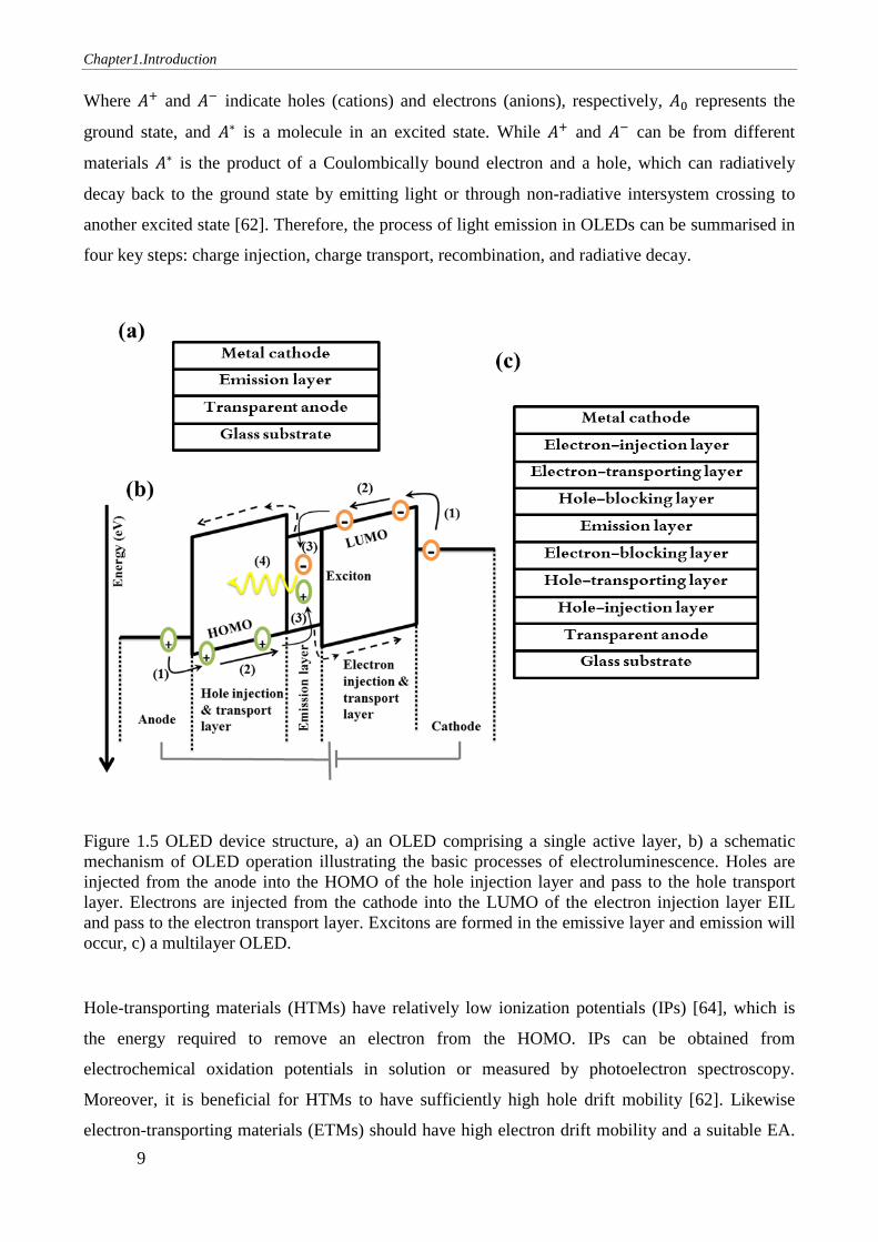
Chapter1.Introduction
9
Where 𝐴+ and 𝐴− indicate holes (cations) and electrons (anions), respectively, 𝐴0 represents the
ground state, and 𝐴∗ is a molecule in an excited state. While 𝐴+ and 𝐴− can be from different
materials 𝐴∗ is the product of a Coulombically bound electron and a hole, which can radiatively
decay back to the ground state by emitting light or through non-radiative intersystem crossing to
another excited state [62]. Therefore, the process of light emission in OLEDs can be summarised in
four key steps: charge injection, charge transport, recombination, and radiative decay.
Figure 1.5 OLED device structure, a) an OLED comprising a single active layer, b) a schematic
mechanism of OLED operation illustrating the basic processes of electroluminescence. Holes are
injected from the anode into the HOMO of the hole injection layer and pass to the hole transport
layer. Electrons are injected from the cathode into the LUMO of the electron injection layer EIL
and pass to the electron transport layer. Excitons are formed in the emissive layer and emission will
occur, c) a multilayer OLED.
Hole-transporting materials (HTMs) have relatively low ionization potentials (IPs) [64], which is
the energy required to remove an electron from the HOMO. IPs can be obtained from
electrochemical oxidation potentials in solution or measured by photoelectron spectroscopy.
Moreover, it is beneficial for HTMs to have sufficiently high hole drift mobility [62]. Likewise
electron-transporting materials (ETMs) should have high electron drift mobility and a suitable EA.
Chapter1.Introduction
10
The EA is the negative of the energy released when an atom or a molecule (X) acquires an electron
to form the negative ion (X-) [62]. EAs can be obtained from the correlation of laser photo-electron
spectroscopy results with the LUMO energy levels.
The performance of OLED devices is typically described by four metrics: drive voltage, efficiency,
lifetime, and colour [62], which are defined as follows:
Drive voltage – also referred to as the turn on voltage, is the voltage that must be applied in order to
have an emission intensity of 1 cd/m2. This voltage is affected by a variety of factors: the built in
potential between electrodes; energetic barriers to charge injection; and the electric field which is
required for migration of charge carriers through the device [62]. Therefore, in a well-optimised
device, the turn on voltage will approach the energy of the emitted photons [65]. Moreover, the turn
on voltage can be reduced by careful selection of the EML, electron transport layer (ETL), and hole
transport layer (HTL) materials so that the energy barriers for charge injection from the transport
layer into the EML are minimised [62].
Efficiency – is defined as the ratio of output light energy to the energy input or electrical energy
expended [66]. This can be represented by a variety of metrics: external quantum efficiency (EQE),
current efficiency (cd/A), and power efficiency (lm/W), which will be described in the next chapter.
Lifetime – sometimes referred to as potential stability, is defined as the number of hours required
for the photo-intensity of the device to drop to half of its initial value at a given current density.
Device failure occurs for several reasons: the degradation of the interface between the metallic
electrodes and the organic layers; chemical reactions from current flow; internal heating of device at
high current densities; and changes in the film morphology of the organic layers [62]. Testing
current densities are typically around 80 mA/cm2 or the current required to generate 1000 cd/m
2
photo-intensity. Lifetime and current density are related with an inverse exponential, therefore
doubling current density leads to a drop factor of 3-4 in lifetime [62].
Colour – is defined according to the 1931 International Commission for Illumination (Commission
Internationale de I’Eclairage) CIEx,y values [67]. The entire emission spectrum of a device is
reduced to two numbers which describe the colour as perceived by the human eye. According to the
National Television Standard Committee (NTSC), the CIE co-ordinates are (0.14, 0.08) for blue,
(0.21, 0.71) for green, (0.67, 0.33) for red, and approximately (0.33, 0.33) for white [62].
There are other additional performance metrics that can affect one or more of the parameters
above such as increasing drive voltage, power consumption, and change in emission colour with age
of the device. Different techniques to optimize the performance metrics of devices include [62]:
Chapter1.Introduction
11
Introducing additional functional layers to the device (see Figure 1.5. c) such as: hole
injection layers (HILs); electron injection layers (EILs); hole blocking layers (HBLs); and
electron blocking layers (EBLs). HIL and EIL improve the injection of holes and electrons,
respectively, into the transporting layers. The blocking layers can also provide more
efficient recombination by confining the electrons and holes in the EML.
Introducing an ETL comprising multiple layers with different LUMO levels to decrease the
drive voltage, and increase the lifetime and efficiency [68].
Increasing the work function of indium tin oxide (ITO), the most commonly used
transparent anode, in order to reduce the injection barrier and consequently the drive
voltage. Various surface treatments produce this effect such as oxygen (O2) plasma
treatment [69], UV/ozone treatment [70], CF4/O2 plasma treatment [71], and treatment with
polymerization of CHF3 [72].
Device stability and efficiency can be improved by the introduction of various hole
injection materials (HIMs) between anode and HTL [73-75]. This would ease the injection
of holes into the HTL. The most common HIM is poly(3,4-ethylenedioxythiphene)
(PEDOT) [76], which is used in the work presented in this thesis.
Charge injection from reactive cathodes such as aluminium to the ETL can be improved by
utilising reactive low work function electron injection materials (EIMs) such as lithium
fluoride and lithium oxide [72, 77].
Introducing host materials into the EML to provide higher recombination rates and reduce
the quenching rate by the dopant (guest) molecules. Host materials need to meet several
requirements such as lower barriers for charge injection, good transport for both electrons
and holes, a wider gap between their HOMO and LUMO than the dopant, and slower non-
radiative decay rates than the time required for energy transfer to the dopant. In order to
meet all of these requirements multiple materials may be used as a mixed host.
The performance metrics of OLED devices such as drive voltage, lifetime, efficiency, and
colour are controlled by complex interactions between different layers in a device. Whilst the
development of new materials for each of these layers is therefore crucial, the interplay between the
properties of these new materials that leads to efficient devices should be borne in mind.
1.5.2 Loss mechanism and dipole orientation in OLEDs
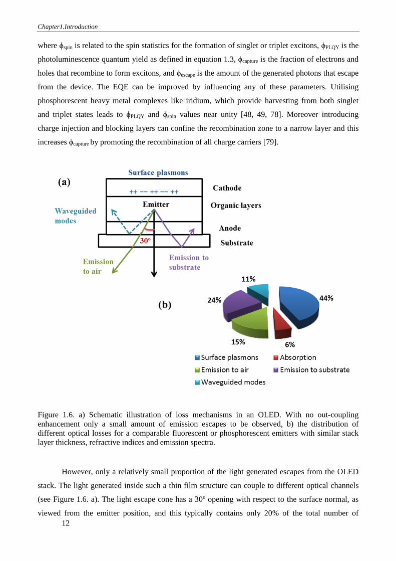
The external quantum efficiency of an OLED is given by
ϕEQE = ϕescape × ϕcapture × ϕspin × ϕPLQY ∗ 100% (1.5)
Chapter1.Introduction
12
where ϕspin is related to the spin statistics for the formation of singlet or triplet excitons, ϕPLQY is the
photoluminescence quantum yield as defined in equation 1.3, ϕcapture is the fraction of electrons and
holes that recombine to form excitons, and ϕescape is the amount of the generated photons that escape
from the device. The EQE can be improved by influencing any of these parameters. Utilising
phosphorescent heavy metal complexes like iridium, which provide harvesting from both singlet
and triplet states leads to ϕPLQY and ϕspin values near unity [48, 49, 78]. Moreover introducing
charge injection and blocking layers can confine the recombination zone to a narrow layer and this
increases ϕcapture by promoting the recombination of all charge carriers [79].
Figure 1.6. a) Schematic illustration of loss mechanisms in an OLED. With no out-coupling
enhancement only a small amount of emission escapes to be observed, b) the distribution of
different optical losses for a comparable fluorescent or phosphorescent emitters with similar stack
layer thickness, refractive indices and emission spectra.
However, only a relatively small proportion of the light generated escapes from the OLED
stack. The light generated inside such a thin film structure can couple to different optical channels
(see Figure 1.6. a). The light escape cone has a 30º opening with respect to the surface normal, as
viewed from the emitter position, and this typically contains only 20% of the total number of
Chapter1.Introduction
13
photons [80, 81]. At higher emission angles, the light cannot even reach the glass substrate as it will
be reflected back by the other organic layers and the transparent ITO electrode before finally being
lost by re-absorption or emission at the edge of the device [81]. The light generated can also couple
to surface plasmon polaritons (SPPs), infrared- or visible-frequency electromagnetic waves
traveling along a metal-dielectric or metal-air interface. The term "surface plasmon polariton"
explains that the wave involves both charge motion in the metal ("surface plasmon") and
electromagnetic waves in the air or dielectric ("polariton" ) [82, 83]. In typical planar OLED stacks
around 60% of the light is trapped in plasmon and waveguided modes within the device [84-86].
Figure 1.6 b) shows the contribution of different optical losses for the fluorescent emitter Alq3 and
these losses would be similar for any fluorescent or phosphorescent emitter with comparable stack
layer thicknesses, refractive indices and emission spectra [81].
Different approaches to improve out-coupling have been reported including high refractive
index substrates [8, 88], grating-assisted out-coupling [89-91] and many others [81, 92]. An
alternative strategy is to intrinsically increase the out-coupling by controlling the direction of light
emission. This utilises the fact that light is emitted perpendicular to the dipole transition moment
vector of the organometallic molecules at the centre of these devices [93, 94]. Orientation of the
transition dipoles parallel to the substrate eliminates the need for gratings, micro-lens arrays, or any
other physical methods used to enhance out-coupling [4, 8, 88, 93, 95, 96]. Moreover, this strategy
avoids the excitation of surface plasmons even when the emitter is close to the metallic electrode
[81].
To have horizontally oriented dipoles, the emitter molecules must have anisotropic
orientations. Some materials have intrinsically rod-like chromophores with large shape anisotropy
[97]. This effect has been well known for polymeric OLEDs [98, 99], fluorescent emitters [97, 100],
and even phosphorescent emitters doped in isotropic materials [101]. The orientation depends on
the anisotropic property of the host or dopant in an emissive layer and also the packing within such
host-guest systems [102-104].
Amorphous organic semiconductor films cannot be analysed by X-ray diffraction
measurements as they do not have a long-range periodic structure. However, there are some
methods which quantitatively estimate the degree of molecular orientation in amorphous organic
films including: variable angle spectroscopic ellipsometry [93]; absorption spectra from
randomization of molecular orientation induced by heating [105]; and angular dependent PL
spectrum measurements [81, 106, 107]. The last method was used in the work presented in this
thesis.
Chapter1.Introduction
14
Figure 1. 7 a) The conventional definition for dipole orientation, b) A cross-sectional schematic
view of the angular dependent PL spectrum set up , c) A schematic diagram of the experimental
setup with angle notations and emission polarizer orientations for recording s- and p- polarized
emission, adapted from [87].
Figures 1.7 a) and b) illustrate the co-ordinate system and an outline of the angle dependent
PL measurement apparatus. Isotropic materials with random transition dipole orientations are
treated as a superposition of px-, py-, and pz- dipoles with each contributing a third of the emitted
intensity. For a perfectly isotropic material the ratio of perpendicular (pz) and parallel (px- and py-)
polarised waves is therefore 33:67, while the horizontally oriented dipoles consist of equal
proportions of px- and py-dipoles [107]. Given that the dipoles radiate strongest perpendicular to
their oscillation direction, the pz-dipoles emit mainly at large angles between 0◦ to 180
◦ (see Figure
1.7 c). Emission from pz-dipoles leads to loss in plasmons and waveguided modes, therefore out
coupling efficiency can be increased by converting vertical dipoles to horizontal dipoles. To obtain
information about the ratio of horizontal and vertical dipoles the p-polarized emission in the x-z
plane is measured. The p-polarized plane is parallel to the detector (or incident) plane, which is
perpendicular to the substrate. The py-dipoles have no component in the p-polarized emission due to
Chapter1.Introduction
15
the fact that they are vertical in the detector plane. Taking into account that px-dipoles emit between
90◦ to 270
◦ in the detector plane, measuring the p-polarized emission consequently yields
information about the existence of vertical emission. The experimental technique of angular
dependent PL spectrum measurements will be detailed in the next chapter.
1.6 Organic light emitting field effect transistors
An organic field-effect transistor is a three terminal device with switching properties
comprising gate, source and drain electrodes, with dielectric and semiconductor layers sandwiched
in between. When the switching properties of an OFET were combined with the electroluminescent
properties of an OLED in a single device architecture, a new family of devices was established
called light emitting field effect transistors [10]. The structure of a LEFET is the same as an OFET
except that the semiconductor layer is electroluminescent. This can be achieved by using either a
single layer, or multi-layer LEFET architectures with more than one semiconductor layer (see
Figure 1.8).
1.6.1 Operating mechanism, parameters, and performance metrices
The two important architectural parameters in a LEFET are the channel length (L, the
distance between source and drain electrodes) and the channel width (W, the length of the source or
drain electrodes). LEFETs can be operated in three different modes depending on the type of charge
transport occurring in the device: i) unipolar p-type in which transport is dominated by holes; ii)
unipolar n-type in which transport is dominated by electrons; and iii) ambipolar mode in which both
electrons and holes can accumulate and be transported within the semiconducting channel of the
device [108].
The basic operating mechanism of LEFETs is based on that of OFETs, where charges are
accumulated at the semiconductor/dielectric interface in order to switch the device ON. This is
referred to as accumulation mode because most organic semiconductors are intrinsically undoped in
contrast to inorganic semiconductors that can be extrinsically doped [23].
In the case of the unipolar p-type mode (see Figure 1.7. a), the application of negative gate
voltage (VG) polarises the dielectric, which builds a capacitance and leads to the accumulation of
positive charge carriers (holes) at the semiconductor/dielectric interface. The application of a
negative voltage between the source and drain electrodes (VDS) injects electrons and more holes into
the LUMO and HOMO of the semiconductor layer, respectively. The injected holes accumulate at
the interface between the semiconductor and dielectric and the increase in positive charge carriers

Chapter1.Introduction
16
increases the charge carrier density at the interface to produce a conducting channel inside the
semiconductor.
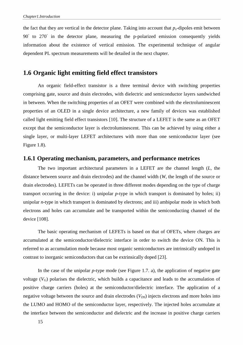
Figure 1.8 Schematic diagrams including the p-type operating mechanisms of a) a single layer
LEFET and b) a multi-layer LEFET.
The current between the source and drain electrodes (IDS) increases when the transistor is
switched ON. Holes and electrons that are injected by the source and drain electrodes can
recombine during device operation and light is consequently emitted from the channel. Although in
a unipolar LEFET just one type of charge carrier accumulates within the channel, both charge
carriers need to be injected in order for light emission to occur. These criteria can be achieved using
either a single layer, where charge transport and recombination occur in the same layer, or multi-
layer LEFET architectures, in which charge transport and recombination occur in separate layers
(see Figure 1.8 b). Operation in an n-type LEFET is the same as in a p-type LEFET except that the
applied voltages are positive and electrons are the dominant charge carriers.
In case of an ambipolar LEFET, both charge carriers can be transported in the channel
depending on the polarity of the applied voltage [109]. The source and drain electrodes can be
symmetric or asymmetric (comprised of high and low work function electrodes) depending on the
Chapter1.Introduction
17
semiconductor layer. There are also different operating regimes of a single layer ambipolar LEFET,
which are detailed as follows:
Electron-dominated regime – electrons are the dominant charge transport carrier within the
transistor channel with a large positive applied gate voltage. Holes are injected into the
semiconductor layer and remain in the vicinity of the hole-injecting contact. As more
electrons accumulate at the interface, they recombine with holes near the hole-injecting
contact to emit light [110]. The source-drain current and consequently the brightness of the
device are consequently high.
Ambipolar regime – as the gate voltage approaches zero and toward negative direction, the
accumulation of electrons decreases and begins to be replaced partly by the holes. Holes and
electrons are therefore both accumulated throughout the channel and their currents are more
balanced. Light emission will occur in the middle of the transistor channel and with lower
intensity than in the single-charge dominated regimes [23, 111].
Hole-dominated regime – when the gate voltage becomes large and negative, holes
accumulate the channel. At the same time electrons are injected into device and remain in
the vicinity of the electron-injecting contact. Holes recombine with electrons close to the
electron-injecting contact and produce a high brightness as was the case in the electron-
dominated regime [110].
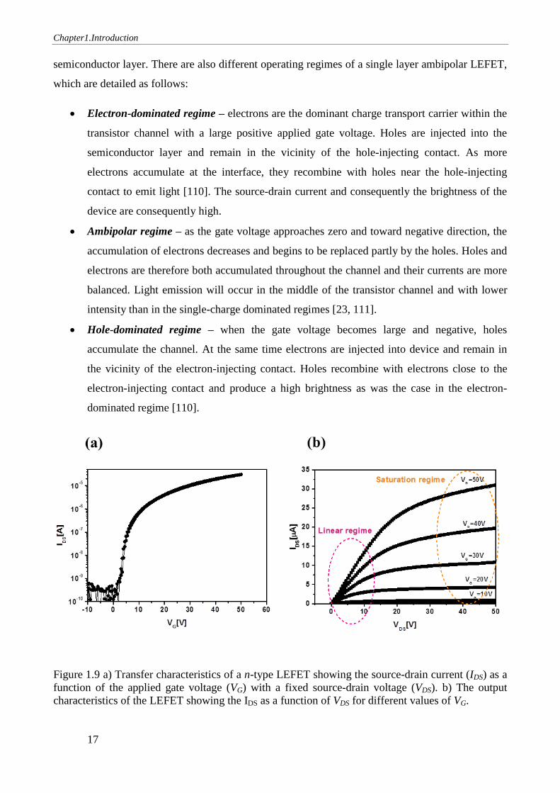
Figure 1.9 a) Transfer characteristics of a n-type LEFET showing the source-drain current (IDS) as a
function of the applied gate voltage (VG) with a fixed source-drain voltage (VDS). b) The output
characteristics of the LEFET showing the IDS as a function of VDS for different values of VG.
Chapter1.Introduction
18
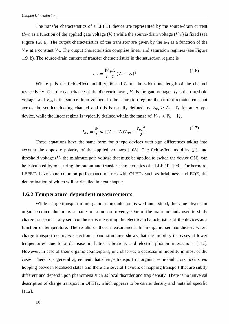
The transfer characteristics of a LEFET device are represented by the source-drain current
(IDS) as a function of the applied gate voltage (VG) while the source-drain voltage (VDS) is fixed (see
Figure 1.9. a). The output characteristics of the transistor are given by the IDS as a function of the
VDS at a constant VG. The output characteristics comprise linear and saturation regimes (see Figure
1.9. b). The source-drain current of transfer characteristics in the saturation regime is
𝐼𝐷𝑆 =
𝑊
𝐿
𝜇𝐶
2(𝑉𝐺 − 𝑉𝑡)2
(1.6)
Where µ is the field-effect mobility, W and L are the width and length of the channel
respectively, C is the capacitance of the dielectric layer, VG is the gate voltage, Vt is the threshold
voltage, and VDS is the source-drain voltage. In the saturation regime the current remains constant
across the semiconducting channel and this is usually defined by 𝑉𝐷𝑆 ≥ 𝑉𝐺 − 𝑉𝑡 for an n-type
device, while the linear regime is typically defined within the range of 𝑉𝐷𝑆 < 𝑉𝐺 − 𝑉𝑡.
𝐼𝐷𝑆 =
𝑊
𝐿𝜇𝑐[(𝑉𝐺 − 𝑉𝑡)𝑉𝐷𝑆 −
𝑉𝐷𝑆2
2]
(1.7)
These equations have the same form for p-type devices with sign differences taking into
account the opposite polarity of the applied voltages [108]. The field-effect mobility (µ), and
threshold voltage (Vt, the minimum gate voltage that must be applied to switch the device ON), can
be calculated by measuring the output and transfer characteristics of a LEFET [108]. Furthermore,
LEFETs have some common performance metrics with OLEDs such as brightness and EQE, the
determination of which will be detailed in next chapter.
1.6.2 Temperature-dependent measurements
While charge transport in inorganic semiconductors is well understood, the same physics in
organic semiconductors is a matter of some controversy. One of the main methods used to study
charge transport in any semiconductor is measuring the electrical characteristics of the devices as a
function of temperature. The results of these measurements for inorganic semiconductors where
charge transport occurs via electronic band structures shows that the mobility increases at lower
temperatures due to a decrease in lattice vibrations and electron-phonon interactions [112].
However, in case of their organic counterparts, one observes a decrease in mobility in most of the
cases. There is a general agreement that charge transport in organic semiconductors occurs via
hopping between localized states and there are several flavours of hopping transport that are subtly
different and depend upon phenomena such as local disorder and trap density. There is no universal
description of charge transport in OFETs, which appears to be carrier density and material specific
[112].
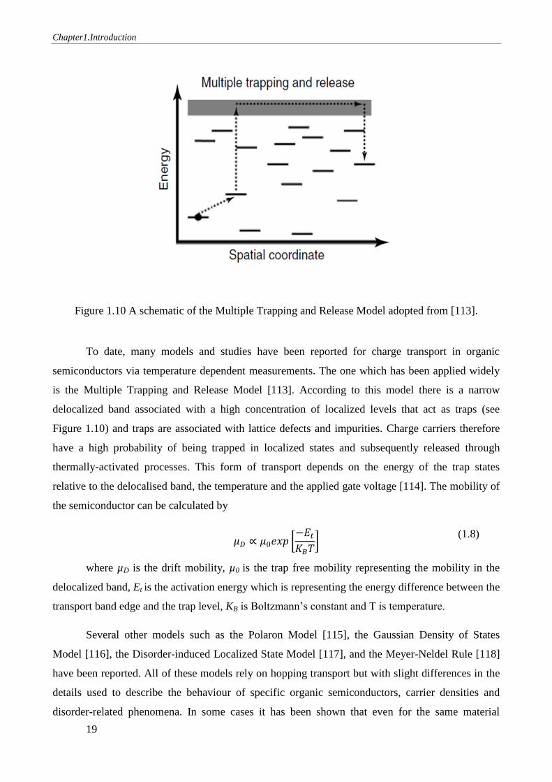
Chapter1.Introduction
19
Figure 1.10 A schematic of the Multiple Trapping and Release Model adopted from [113].
To date, many models and studies have been reported for charge transport in organic
semiconductors via temperature dependent measurements. The one which has been applied widely
is the Multiple Trapping and Release Model [113]. According to this model there is a narrow
delocalized band associated with a high concentration of localized levels that act as traps (see
Figure 1.10) and traps are associated with lattice defects and impurities. Charge carriers therefore
have a high probability of being trapped in localized states and subsequently released through
thermally-activated processes. This form of transport depends on the energy of the trap states
relative to the delocalised band, the temperature and the applied gate voltage [114]. The mobility of
the semiconductor can be calculated by
𝜇𝐷 ∝ 𝜇0𝑒𝑥𝑝 [
−𝐸𝑡
𝐾𝐵𝑇]
(1.8)
where µD is the drift mobility, µ0 is the trap free mobility representing the mobility in the
delocalized band, Et is the activation energy which is representing the energy difference between the
transport band edge and the trap level, KB is Boltzmann’s constant and T is temperature.
Several other models such as the Polaron Model [115], the Gaussian Density of States
Model [116], the Disorder-induced Localized State Model [117], and the Meyer-Neldel Rule [118]
have been reported. All of these models rely on hopping transport but with slight differences in the
details used to describe the behaviour of specific organic semiconductors, carrier densities and
disorder-related phenomena. In some cases it has been shown that even for the same material
Chapter1.Introduction
20
different morphologies lead to different charge transport behaviour. As an example, the charge
transport mechanism in pentacene has been explored using the transistor structure. Vapour
deposited pentacene films displayed mobilities that were nearly independent of temperature [119]
whereas solution-processed pentacene films show a strong dependence of the mobility on
temperature [120]. These results highlight the challenges in studying the transport physics of
organic semiconductors. All of the reports of temperature dependent measurements on organic
semiconductors were performed using OFET structures. However, there are as yet no reports of
combined studies into charge transport and recombination simultaneously in LEFET structures and
this motivated the work presented in Chapter 6 of this thesis.
1.7 Aims of this project
Although organic light emitting devices have found their way into the display industry there
is still a need for higher efficiency and easier mass production methods and great steps have been
taken towards fully understanding organic semiconductors, which can pave the way to these goals.
However, there are still significant opportunities for better understanding the structure-property
relationships in organic semiconductors as they relate to OLEDs and LEFETs. This knowledge can
lead to new chemical structure design of materials that provide better photo-physical and electrical
properties. The invention of new classes of organic emissive semiconductors termed dendrimers
provides better independent control over luminescent and transport properties. The three
dimensional tree-like shapes of these materials can provide engineering of their branches
responsible for molecular interaction, solubility, and viscosity which are useful tuning parameters
for mass production techniques. Furthermore, desirable packing of molecules within the emissive
layer may provide intentional orientation of dipoles which directly enhances the out-coupling in
devices. The aims of this project are therefore three fold:
1. To study the photo-physics and dipole orientation in light emitting dendrimers and poly-
dendrimers.
2. To develop an understanding of radiative recombination processes with molecular structure
in dendrimers and poly(dendrimers) OLEDs.
3. To investigate the charge transport, charge injection and recombination physics in LEFET
devices.
Chapter 2 will outline the systematic characterisation techniques of the materials to be tested,
followed by fabrication and characterisation techniques for the OLED and LEFET devices used
throughout the work presented in this thesis. Chapter 3 details an introduction and overview of
Chapter1.Introduction
21
devices incorporating solution-processable dendrimers. This was the first time that an OLED device
with neat emissive layer was demonstrated with a similar EQE to blended counterparts. The photo-
physical and device characterisations are further investigated in chemically modified versions of the
parent material these results are described in Chapters 4 and 5. In Chapter 4 the fundamental
benefits of the dendrimer system are described and the effects of dendrimer generation and type of
dendron are presented. Furthermore, the effect of polymerisation of the dendrimers to form
poly(dendrimer)s, promising materials for inkjet printing, will be outlined. The introduction of both
electron- and hole-transporting moieties to form ambipolar co-polymers will also be discussed
along with their photo-physical and electrical properties in Chapter 5. The work presented in this
thesis culminates in Chapter 6, which describes temperature dependent measurement on LEFETs.
Finally, Chapter 7 summarises the findings of the work presented in this thesis, and the potential
future for light emitting devices.
Chapter1.Introduction
22
References
[1] http://www.digitaltrends.com/home-theater/the-future-of-seen-rollable-oled-displays/.
[2] S.G. Stevenson, Dendrimer light-emitting diodes, in, University of St Andrews, 2008.
[3] http://raqwe.blogspot.com.au/2013/10/iwatch-will-have-flexible-oled-display.html.
[4] S.R. Forrest, The path to ubiquitous and low-cost organic electronic appliances on plastic,
Nature, 428 (2004) 911-918.
[5] A. Smith, Properties of Materials for Organic Light Emitting Diodes, (2011).
[6] R.M. News Samsung, 2011, http://www.samsung.com/us/news/newsRead.do?news_seq=19806.
[7] J. Kido, M. Kimura, K. Nagai, Multilayer white light-emitting organic electroluminescent
device, Science, 267 (1995) 1332-1334.
[8] S. Reineke, F. Lindner, G. Schwartz, N. Seidler, K. Walzer, B. Lüssem, K. Leo, White organic
light-emitting diodes with fluorescent tube efficiency, Nature, 459 (2009) 234-238.
[9] M.C. Gather, A. Köhnen, K. Meerholz, White Organic Light‐Emitting Diodes, Advanced
Materials, 23 (2011) 233-248.
[10] E.B. Namdas, J.S. Swensen, P. Ledochowitsch, J.D. Yuen, D. Moses, A.J. Heeger, Gate‐Controlled Light Emitting Diodes, Advanced Materials, 20 (2008) 1321-1324.
[11] K. Nakamura, T. Hata, A. Yoshizawa, K. Obata, H. Endo, K. Kudo, Improvement of metal–
insulator–semiconductor-type organic light-emitting transistors, Japanese Journal of Applied
Physics, 47 (2008) 1889.
[12] E.B. Namdas, M. Tong, P. Ledochowitsch, S.R. Mednick, J.D. Yuen, D. Moses, A.J. Heeger,
Low thresholds in polymer lasers on conductive substrates by distributed feedback nanoimprinting:
progress toward electrically pumped plastic lasers, Advanced materials, 21 (2009) 799-802.
[13] M.C. Gwinner, S. Khodabakhsh, M.H. Song, H. Schweizer, H. Giessen, H. Sirringhaus,
Integration of a Rib Waveguide Distributed Feedback Structure into a Light‐Emitting Polymer
Field‐Effect Transistor, Advanced Functional Materials, 19 (2009) 1360-1370.
[14] T. Matsushita, T. Asada, S. Koseki, Relativistic study on emission mechanism in tris (2-
phenylpyridine) iridium, The Journal of Physical Chemistry C, 111 (2007) 6897-6903.
[15] F. De Angelis, S. Fantacci, N. Evans, C. Klein, S.M. Zakeeruddin, J.-E. Moser, K.
Kalyanasundaram, H.J. Bolink, M. Grätzel, M.K. Nazeeruddin, Controlling phosphorescence color
and quantum yields in cationic iridium complexes: a combined experimental and theoretical study,
Inorganic chemistry, 46 (2007) 5989-6001.
[16] K. Nozaki, Theoretical Studies on Photophysical Properties and Mechanism of
Phosphorescence in [fac‐Ir (2‐phenylpyridine) 3], Journal of the Chinese Chemical Society, 53
(2006) 101-112.
[17] K. Nozaki, K. Takamori, Y. Nakatsugawa, T. Ohno, Theoretical studies of phosphorescence
spectra of tris (2, 2'-bipyridine) transition metal compounds, Inorganic chemistry, 45 (2006) 6161-
6178.
[18] S. Obara, M. Itabashi, F. Okuda, S. Tamaki, Y. Tanabe, Y. Ishii, K. Nozaki, M.-a. Haga,
Highly phosphorescent iridium complexes containing both tridentate bis (benzimidazolyl)-benzene
or-pyridine and bidentate phenylpyridine: Synthesis, photophysical properties, and theoretical study
of Ir-bis (benzimidazolyl) benzene complex, Inorganic chemistry, 45 (2006) 8907-8921.
[19] T. Yutaka, S. Obara, S. Ogawa, K. Nozaki, N. Ikeda, T. Ohno, Y. Ishii, K. Sakai, M.-a. Haga,
Syntheses and properties of emissive iridium (III) complexes with tridentate benzimidazole
derivatives, Inorganic chemistry, 44 (2005) 4737-4746.
[20] T.D. Anthopoulos, M.J. Frampton, E.B. Namdas, P.L. Burn, I.D. Samuel, Solution‐
Processable Red Phosphorescent Dendrimers for Light‐Emitting Device Applications, Advanced
Materials, 16 (2004) 557-560.
Chapter1.Introduction
23
[21] S.-C. Lo, E. Namdas, P. Burn, I. Samuel, Synthesis and properties of highly efficient
electroluminescent green phosphorescent iridium cored dendrimers, Macromolecules, 36 (2003)
9721-9730.
[22] S.-C. Lo, C.P. Shipley, R.N. Bera, R.E. Harding, A.R. Cowley, P.L. Burn, I.D. Samuel, Blue
phosphorescence from iridium (III) complexes at room temperature, Chemistry of materials, 18
(2006) 5119-5129.
[23] A.J. Heeger, N.S. Sariciftci, E.B. Namdas, Semiconducting and metallic polymers, Oxford
University Press, 2010.
[24] K.E. Mutkins, Organic field-effect transistors based on dendrimers and small molecules,
(2012).
[25] W. Brütting, Physics of organic semiconductors, John Wiley & Sons, 2006.
[26] C.W. Tang, S.A. VanSlyke, Organic electroluminescent diodes, Applied physics letters, 51
(1987) 913-915.
[27] M. Baldo, M. Thompson, S. Forrest, High-efficiency fluorescent organic light-emitting devices
using a phosphorescent sensitizer, Nature, 403 (2000) 750-753.
[28] M. Baldo, M. Deutsch, P. Burrows, H. Gossenberger, M. Gerstenberg, V. Ban, S. Forrest,
Organic vapor phase deposition, Advanced Materials, 10 (1998) 1505-1514.
[29] M. Shtein, P. Peumans, J.B. Benziger, S.R. Forrest, Direct mask-free patterning of molecular
organic semiconductors using organic vapor jet printing, Journal of applied physics, 96 (2004)
4500-4507.
[30] Y. Sun, M. Shtein, S.R. Forrest, Direct patterning of organic light-emitting devices by organic-
vapor jet printing, Applied Physics Letters, 86 (2005) 113504.
[31] M. Halim, I. Samuel, J. Pillow, A. Monkman, P. Burn, Control of colour and charge injection
in conjugated dendrimer/polypyridine bilayer LEDs, Synthetic metals, 102 (1999) 1571-1574.
[32] M. Halim, J.N. Pillow, I.D. Samuel, P.L. Burn, Conjugated Dendrimers for Light‐Emitting
Diodes: Effect of Generation, Advanced Materials, 11 (1999) 371-374.
[33] M. Halim, J. Pillow, I. Samuel, P. Burn, The effect of dendrimer generation on LED efficiency,
Synthetic metals, 102 (1999) 922-923.
[34] M. Halim, I. Samuel, J. Pillow, P. Burn, Conjugated dendrimers for LEDs: Control of colour,
Synthetic metals, 102 (1999) 1113-1114.
[35] J. Pillow, P. Burn, I. Samuel, M. Halim, Synthetic routes to phenylene vinylene dendrimers,
Synthetic metals, 102 (1999) 1468-1469.
[36] J.N. Pillow, M. Halim, J.M. Lupton, P.L. Burn, I.D. Samuel, A facile iterative procedure for
the preparation of dendrimers containing luminescent cores and stilbene dendrons, Macromolecules,
32 (1999) 5985-5993.
[37] K.A. Knights, S.G. Stevenson, C.P. Shipley, S.-C. Lo, S. Olsen, R.E. Harding, S. Gambino,
P.L. Burn, I.D. Samuel, A rapid route to carbazole containing dendrons and phosphorescent
dendrimers, Journal of Materials Chemistry, 18 (2008) 2121-2130.
[38] S. Gambino, S.G. Stevenson, K.A. Knights, P.L. Burn, I.D. Samuel, Control of Charge
Transport in Iridium (III) Complex‐Cored Carbazole Dendrimers by Generation and Structural
Modification, Advanced Functional Materials, 19 (2009) 317-323.
[39] J. Lupton, I.D. Samuel, R. Beavington, P.L. Burn, H. Bässler, Control of Charge Transport and
Intermolecular Interaction in Organic Light‐Emitting Diodes by Dendrimer Generation, Advanced
Materials, 13 (2001) 258-261.
[40] M.J. Frampton, S.W. Magennis, J.N. Pillow, P.L. Burn, I.D. Samuel, The effect of
intermolecular interactions on the electro-optical properties of porphyrin dendrimers with
conjugated dendrons, Journal of Materials Chemistry, 13 (2003) 235-242.
[41] J. Lupton, I. Samuel, R. Beavington, M. Frampton, P. Burn, H. Bässler, Control of mobility in
molecular organic semiconductors by dendrimer generation, Physical Review B, 63 (2001) 155206.
Chapter1.Introduction
24
[42] T.D. Anthopoulos, J.P. Markham, E.B. Namdas, J.R. Lawrence, I.D. Samuel, S.-C. Lo, P.L.
Burn, Influence of molecular structure on the properties of dendrimer light-emitting diodes, Organic
electronics, 4 (2003) 71-76.
[43] G. Hayes, I. Samuel, R. Phillips, Ultrafast dynamics of photoexcitations in conjugated
polymers, Synthetic metals, 84 (1997) 889-890.
[44] G. Lanzani, G. Cerullo, C. Brabec, N. Sariciftci, Time domain investigation of the intrachain
vibrational dynamics of a prototypical light-emitting conjugated polymer, Physical review letters,
90 (2003) 047402.
[45] J.-P.R. Wells, D.G. Lidzey, P.J. Phillips, D.A. Carder, A.M. Fox, Ultrafast measurements of
vibrational relaxation in the conjugated polymer poly (9, 9-dioctylfluorene), Applied physics letters,
85 (2004) 3080-3082.
[46] N. Greenham, I. Samuel, G. Hayes, R. Phillips, Y. Kessener, S. Moratti, A. Holmes, R. Friend,
Measurement of absolute photoluminescence quantum efficiencies in conjugated polymers,
Chemical physics letters, 241 (1995) 89-96.
[47] K.-C. Tang, K.L. Liu, I.-C. Chen, Rapid intersystem crossing in highly phosphorescent iridium
complexes, Chemical physics letters, 386 (2004) 437-441.
[48] M.A. Baldo, D. O'brien, Y. You, A. Shoustikov, S. Sibley, M. Thompson, S. Forrest, Highly
efficient phosphorescent emission from organic electroluminescent devices, Nature, 395 (1998)
151-154.
[49] M. Baldo, S. Lamansky, P. Burrows, M. Thompson, S. Forrest, Very high-efficiency green
organic light-emitting devices based on electrophosphorescence, Applied Physics Letters, 75 (1999)
4.
[50] A. Hayer, A.L. Khan, R.H. Friend, A. Köhler, Morphology dependence of the triplet excited
state formation and absorption in polyfluorene, Physical Review B, 71 (2005) 241302.
[51] O. Korovyanko, R. Österbacka, X.M. Jiang, Z.V. Vardeny, R. Janssen, Photoexcitation
dynamics in regioregular and regiorandom polythiophene films, Physical Review B, 64 (2001)
235122.
[52] B. Kraabel, V. Klimov, R. Kohlman, S. Xu, H. Wang, D. McBranch, Unified picture of the
photoexcitations in phenylene-based conjugated polymers: Universal spectral and dynamical
features in subpicosecond transient absorption, Physical review B, 61 (2000) 8501.
[53] R. Joseph, Lakowicz. Principles of fluorescence spectroscopy, in, Springer, 2006.
[54] M. Baldo, D. O’brien, M. Thompson, S. Forrest, Excitonic singlet-triplet ratio in a
semiconducting organic thin film, Physical Review B, 60 (1999) 14422.
[55] R. Friend, R. Gymer, A. Holmes, J. Burroughes, R. Marks, C. Taliani, D. Bradley, D. Dos
Santos, J. Bredas, M. Lögdlund, Electroluminescence in conjugated polymers, Nature, 397 (1999)
121-128.
[56] J. Wilson, A. Dhoot, A. Seeley, M. Khan, A. Köhler, R. Friend, Spin-dependent exciton
formation in π-conjugated compounds, Nature, 413 (2001) 828-831.
[57] M. Segal, M. Baldo, R. Holmes, S. Forrest, Z. Soos, Excitonic singlet-triplet ratios in
molecular and polymeric organic materials, Physical Review B, 68 (2003) 075211.
[58] C. Adachi, M.A. Baldo, M.E. Thompson, S.R. Forrest, Nearly 100% internal phosphorescence
efficiency in an organic light-emitting device, Journal of Applied Physics, 90 (2001) 5048-5051.
[59] Y. Kawamura, K. Goushi, J. Brooks, J.J. Brown, H. Sasabe, C. Adachi, 100% phosphorescence
quantum efficiency of Ir (III) complexes in organic semiconductor films, Applied Physics Letters,
86 (2005) 71104-71104.
[60] G.A. Crosby, J.N. Demas, Measurement of photoluminescence quantum yields. Review, The
Journal of Physical Chemistry, 75 (1971) 991-1024.
[61] P.E. Shaw, Measurements of exciton diffusion in conjugated polymers, in, University of St
Andrews, 2009.
[62] F. So, Organic electronics: materials, processing, devices and applications, CRC press, 2009.
Chapter1.Introduction
25
[63] C. Tang, S. VanSlyke, C. Chen, Electroluminescence of doped organic thin films, Journal of
Applied Physics, 65 (1989) 3610-3616.
[64] Y. Shirota, H. Kageyama, Charge carrier transporting molecular materials and their
applications in devices, Chemical reviews, 107 (2007) 953-1010.
[65] V.V. Jarikov, D.Y. Kondakov, C.T. Brown, Efficient and extremely long-lived organic light-
emitting diodes based on dinaphthylperylene, Journal of Applied Physics, 102 (2007) 104908.
[66] S.R. Forrest, D.D. Bradley, M.E. Thompson, Measuring the Efficiency of Organic Light‐Emitting Devices, Advanced Materials, 15 (2003) 1043-1048.
[67] T. Smith, J. Guild, The CIE colorimetric standards and their use, Transactions of the Optical
Society, 33 (1931) 73.
[68] W.J. Begley, T.K. Hatwar, 36.2: High‐Performing Organic Electron‐Injecting and
Transporting Layers for Red, Green, Blue, and White OLED Devices, in: SID Symposium Digest
of Technical Papers, Wiley Online Library, 2007, pp. 1286-1289.
[69] C. Wu, C. Wu, J. Sturm, A. Kahn, Surface modification of indium tin oxide by plasma
treatment: An effective method to improve the efficiency, brightness, and reliability of organic light
emitting devices, Applied Physics Letters, 70 (1997) 1348-1350.
[70] M. Mason, L.S. Hung, C. Tang, S. Lee, K. Wong, M. Wang, Characterization of treated
indium–tin–oxide surfaces used in electroluminescent devices, Journal of applied physics, 86
(1999) 1688-1692.
[71] I.-M. Chan, F.C.-N. Hong, Plasma treatments of indium tin oxide anodes in carbon
tetrafluorinde (CF 4)/oxygen (O 2) to improve the performance of organic light-emitting diodes,
Thin Solid Films, 444 (2003) 254-259.
[72] L. Hung, L. Zheng, M. Mason, Anode modification in organic light-emitting diodes by low-
frequency plasma polymerization of CHF3, Applied Physics Letters, 78 (2001) 673.
[73] X. Wang, P. Rundle, M. Bale, A. Mosley, Improved operating lifetime of phosphorescent
OLED by novel anode coating, Synthetic metals, 137 (2003) 1051-1052.
[74] T.P. Saragi, T. Spehr, A. Siebert, T. Fuhrmann-Lieker, J. Salbeck, Spiro compounds for
organic optoelectronics, Chemical reviews, 107 (2007) 1011-1065.
[75] S. Van Slyke, C. Chen, C. Tang, Organic electroluminescent devices with improved stability,
Applied physics letters, 69 (1996) 2160-2162.
[76] J. Kim, M. Granström, R. Friend, N. Johansson, W. Salaneck, R. Daik, W. Feast, F. Cacialli,
Indium–tin oxide treatments for single-and double-layer polymeric light-emitting diodes: The
relation between the anode physical, chemical, and morphological properties and the device
performance, Journal of applied physics, 84 (1998) 6859-6870.
[77] L. Hung, C. Tang, M. Mason, P. Raychaudhuri, J. Madathil, Application of an ultrathin LiF/Al
bilayer in organic surface-emitting diodes, Applied Physics Letters, 78 (2001) 544-546.
[78] H. Yersin, Highly efficient OLEDs with phosphorescent materials, John Wiley & Sons, 2008.
[79] M. Pfeiffer, K. Leo, X. Zhou, J. Huang, M. Hofmann, A. Werner, J. Blochwitz-Nimoth, Doped
organic semiconductors: Physics and application in light emitting diodes, Organic Electronics, 4
(2003) 89-103.
[80] K.A. Neyts, Simulation of light emission from thin-film microcavities, JOSA A, 15 (1998)
962-971.
[81] W. Brütting, J. Frischeisen, T.D. Schmidt, B.J. Scholz, C. Mayr, Device efficiency of organic
light‐emitting diodes: Progress by improved light outcoupling, physica status solidi (a), 210
(2013) 44-65.
[82] S. Zeng, D. Baillargeat, H.-P. Ho, K.-T. Yong, Nanomaterials enhanced surface plasmon
resonance for biological and chemical sensing applications, Chemical Society Reviews, 43 (2014)
3426-3452.
[83] https://en.wikipedia.org/wiki/Surface_plasmon_polariton#cite_note-1.
Chapter1.Introduction
26
[84] S. Nowy, B.C. Krummacher, J. Frischeisen, N.A. Reinke, W. Brütting, Light extraction and
optical loss mechanisms in organic light-emitting diodes: Influence of the emitter quantum
efficiency, Journal of Applied Physics, 104 (2008) 123109.
[85] L.H. Smith, J.A. Wasey, I.D. Samuel, W.L. Barnes, Light Out‐Coupling Efficiencies of
Organic Light‐Emitting Diode Structures and the Effect of Photoluminescence Quantum Yield,
Advanced Functional Materials, 15 (2005) 1839-1844.
[86] S. Nowy, J. Frischeisen, W. Brütting, Simulation based optimization of light-outcoupling in
organic light-emitting diodes, in: SPIE Photonic Devices+ Applications, International Society for
Optics and Photonics, 2009, pp. 74151C-74151C-74159.
[87] S.D. Choudhury, R. Badugu, K. Ray, J.R. Lakowicz, Surface-plasmon induced polarized
emission from Eu (iii)–a class of luminescent lanthanide ions, Chemical Communications, 50
(2014) 9010-9013.
[88] S. Mladenovski, K. Neyts, D. Pavicic, A. Werner, C. Rothe, Exceptionally efficient organic
light emitting devices using high refractive index substrates, Optics Express, 17 (2009) 7562-7570.
[89] W.H. Koo, S.M. Jeong, F. Araoka, K. Ishikawa, S. Nishimura, T. Toyooka, H. Takezoe, Light
extraction from organic light-emitting diodes enhanced by spontaneously formed buckles, Nature
Photonics, 4 (2010) 222-226.
[90] M.K. Callens, H. Marsman, L. Penninck, P. Peeters, H. de Groot, J.M. ter Meulen, K. Neyts,
RCWA and FDTD modeling of light emission from internally structured OLEDs, Optics express,
22 (2014) A589-A600.
[91] C. Fuchs, T. Schwab, T. Roch, S. Eckardt, A. Lasagni, S. Hofmann, B. Lüssem, L. Müller-
Meskamp, K. Leo, M. Gather, Quantitative allocation of Bragg scattering effects in highly efficient
OLEDs fabricated on periodically corrugated substrates, Optics express, 21 (2013) 16319-16330.
[92] K. Saxena, V. Jain, D.S. Mehta, A review on the light extraction techniques in organic
electroluminescent devices, Optical Materials, 32 (2009) 221-233.
[93] D. Yokoyama, Molecular orientation in small-molecule organic light-emitting diodes, Journal
of Materials Chemistry, 21 (2011) 19187-19202.
[94] T.D. Schmidt, D.S. Setz, M. Flämmich, J. Frischeisen, D. Michaelis, B.C. Krummacher, N.
Danz, W. Brütting, Evidence for non-isotropic emitter orientation in a red phosphorescent organic
light-emitting diode and its implications for determining the emitter’s radiative quantum efficiency,
Applied Physics Letters, 99 (2011) 163302.
[95] H. Sasabe, J. Kido, Development of high performance OLEDs for general lighting, Journal of
Materials Chemistry C, 1 (2013) 1699-1707.
[96] H. Sasabe, J. Kido, Recent Progress in Phosphorescent Organic Light‐Emitting Devices,
European Journal of Organic Chemistry, 2013 (2013) 7653-7663.
[97] D. Yokoyama, A. Sakaguchi, M. Suzuki, C. Adachi, Horizontal orientation of linear-shaped
organic molecules having bulky substituents in neat and doped vacuum-deposited amorphous films,
Organic Electronics, 10 (2009) 127-137.
[98] J. Wasey, A. Safonov, I. Samuel, W. Barnes, Effects of dipole orientation and birefringence on
the optical emission from thin films, Optics communications, 183 (2000) 109-121.
[99] M. Flämmich, M.C. Gather, N. Danz, D. Michaelis, A.H. Bräuer, K. Meerholz, A.
Tünnermann, Orientation of emissive dipoles in OLEDs: Quantitative in situ analysis, Organic
Electronics, 11 (2010) 1039-1046.
[100] J. Frischeisen, D. Yokoyama, A. Endo, C. Adachi, W. Brütting, Increased light outcoupling
efficiency in dye-doped small molecule organic light-emitting diodes with horizontally oriented
emitters, Organic Electronics, 12 (2011) 809-817.
[101] M. Flämmich, J. Frischeisen, D.S. Setz, D. Michaelis, B.C. Krummacher, T.D. Schmidt, W.
Brütting, N. Danz, Oriented phosphorescent emitters boost OLED efficiency, Organic Electronics,
12 (2011) 1663-1668.
Chapter1.Introduction
27
[102] K.-H. Kim, S. Lee, C.-K. Moon, S.-Y. Kim, Y.-S. Park, J.-H. Lee, J.W. Lee, J. Huh, Y. You,
J.-J. Kim, Phosphorescent dye-based supramolecules for high-efficiency organic light-emitting
diodes, Nature communications, 5 (2014).
[103] M.J. Jurow, C. Mayr, T.D. Schmidt, T. Lampe, P.I. Djurovich, W. Brütting, M.E. Thompson,
Understanding and predicting the orientation of heteroleptic phosphors in organic light-emitting
materials, Nature materials, (2015).
[104] C.-K. Moon, K.-H. Kim, J.W. Lee, J.-J. Kim, Influence of host molecules on emitting dipole
orientation of phosphorescent iridium complexes, Chemistry of Materials, 27 (2015) 2767-2769.
[105] Y. Sakai, M. Shibata, D. Yokoyama, Simple model-free estimation of orientation order
parameters of vacuum-deposited and spin-coated amorphous films used in organic light-emitting
diodes, Applied Physics Express, 8 (2015) 096601.
[106] S.Y. Kim, W.I. Jeong, C. Mayr, Y.S. Park, K.H. Kim, J.H. Lee, C.K. Moon, W. Brütting, J.J.
Kim, Organic Light‐Emitting Diodes with 30% External Quantum Efficiency Based on a
Horizontally Oriented Emitter, Advanced Functional Materials, 23 (2013) 3896-3900.
[107] J. Frischeisen, D. Yokoyama, C. Adachi, W. Brütting, Determination of molecular dipole
orientation in doped fluorescent organic thin films by photoluminescence measurements, Applied
Physics Letters, 96 (2010) 073302.
[108] Z. Bao, J. Locklin, Organic field-effect transistors, CRC press, 2007.
[109] H. Klauk, Organic electronics II: more materials and applications, John Wiley & Sons, 2012.
[110] J.S. Swensen, J. Yuen, D. Gargas, S.K. Buratto, A.J. Heeger, Light emission from an
ambipolar semiconducting polymer field effect transistor: Analysis of the device physics, Journal of
applied physics, 102 (2007) 013103.
[111] K. Tandy, Active channel field-effect transistors: Towards high performance light emitting
transistors, (2014).
[112] G. Horowitz, Organic field-effect transistors, Advanced Materials, 10 (1998) 365-377.
[113] R. Noriega, A. Salleo, Charge transport theories in organic semiconductors, Organic
Electronics II: More Materials and Applications, 2 (2012).
[114] G. Horowitz, R. Hajlaoui, P. Delannoy, Temperature dependence of the field-effect mobility
of sexithiophene. Determination of the density of traps, Journal de Physique III, 5 (1995) 355-371.
[115] I. Hulea, S. Fratini, H. Xie, C. Mulder, N. Iossad, G. Rastelli, S. Ciuchi, A. Morpurgo,
Tunable Fröhlich polarons in organic single-crystal transistors, Nature Materials, 5 (2006) 982-986.
[116] H. Bässler, Charge transport in disordered organic photoconductors, phys. status solidi b, 175
(1993) 15-56.
[117] N. Mott, E. Davis, Electronic processes in non-crystalline solids, Clarendon, Oxford, (1979)
465.
[118] M. Ullah, PhD dissertation , Johannes Kepler University, Linz (2011).
[119] S. Nelson, Y.-Y. Lin, D. Gundlach, T. Jackson, Temperature-independent transport in high-
mobility pentacene transistors, Applied physics letters, 72 (1998) 1854-1856.
[120] A. Brown, C. Jarrett, D. De Leeuw, M. Matters, Field-effect transistors made from solution-
processed organic semiconductors, Synthetic metals, 88 (1997) 37-55.
28
Chapter 2
Experimental Methods and Equipment
2.1 Introduction
This chapter focuses on describing the characterisation and fabrication techniques for
organic light emitting materials and devices utilised in the research. The first Section of this chapter
details the systematic photo-physical characterisation of organic materials utilizing techniques
including UV-Vis absorption, photo luminescence quantum yield, photo luminescence decay life
time, ellipsometry and dipole orientation measurements. The results of such studies provide better
understanding to optimize device fabrication activities which are described in the next Section of
this chapter. After a brief overview of the primary procedures, device fabrication details will be
given for two different configurations of organic light emitting diodes and light emitting field
effect transistors. Finally, the standard optical and electrical methodologies for characterising light
emitting devices will be described, noting that experiment-specific details will also be provided in
subsequent chapters where relevant.
2.2 Materials
Different classes of material were used in the work described in this thesis including
dendrimers, polymers and small molecules. All dendrimers were synthesised at the centre for
organic photonics and electronics (COPE). These dendrimers were used in OLED devices. The
diketopyrrolopyrrole–dithienothiophene (DPP–DTT) co-polymer was synthesised as described in
reference [1] and used in the LEFET architecture. The commercial small molecules used in the
work described in this thesis were restricted to a choice of 4,4’-N,N’-dicarbazolyl-biphenyl (CBP),
2,2',2"-(1,3,5-Benzinetriyl)-tris(1-phenyl-1-H-benzimidazole) (TPBi) purchased from Lumtec and
co-polymer phenyl-substituted poly(p-phenylenevinylene) knows as Super Yellow (SY) from
Merck. Chemical structures of these materials will be given in relevant chapters.
Chapter2. Experimental Methods and Equipment
29
2.3 Material characteristics
2.3.1 Energy level estimation
Ionisation potentials were measured by photoelectron spectroscopy in air (PESA) in order to
estimate the energy levels (HOMOs) for synthesised materials. Measurements were performed
using Riken Keiki AC-2 spectrometer using 5nW power intensity.
In order to estimate the LUMO energy, optical gaps were appraised from the intersection of
the normalised absorption and solid-state photoluminescent spectra plotted in units of energy (eV).
The optical gaps were then added to the HOMO energies to determine the LUMOs [2]. HOMO and
LUMO then considered in order choosing the best match for host materials and contacts.
2.3.2 Absorption
The results of absorption measurements presented in this thesis were all obtained using a
Cary 5000 UV-Vis spectrophotometer either as in optically dilute solutions in spectroscopic grade
solvent or a thin film on quartz. This equipment was capable of measuring intensity of absorption in
the wavelength range of 800 nm to 200 nm. The instrument contains two channels for reference and
sample. The reference was designed in order to account for any absorption by the solvent or quartz
(in the case of spin-coated films) or cuvette (for solution). Absorbance was calculated through
comparison of transmission (T) of the sample and reference while both illuminated with the same
intensity [2]. Absorbance (A) is then given by the relation
𝐴 = − log(𝑇) (2.1)
2.3.3 Photoluminescence
The photoluminescence spectra of the compounds were measured by a Jobin-Yvon
Fluoromax 4 fluorimeter where a range of excitation wavelengths was provided by a xenon lamp
coupled through a monochromator. Samples were excited at the peak of the absorbance at an angle
of 45 degree and emission was collected for a specific range of wavelengths by a photomultiplier
tube (PMT). PL spectra were then determined after correction for the quantum efficiency of the
PMT by the instrumental software.
Solution samples were made using spectroscopic grade solvent Toluene and were degassed
by three freeze-pump-thaw cycles before measurements [3]. Solid-state neat films were made by
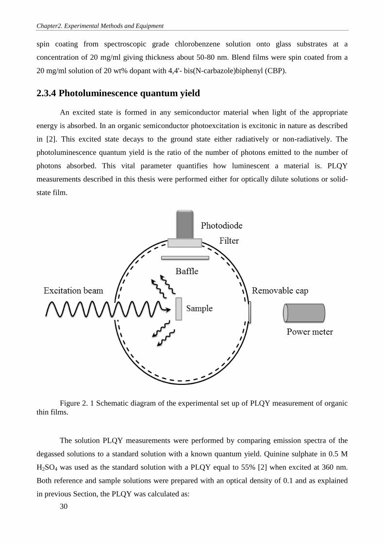
Chapter2. Experimental Methods and Equipment
30
spin coating from spectroscopic grade chlorobenzene solution onto glass substrates at a
concentration of 20 mg/ml giving thickness about 50-80 nm. Blend films were spin coated from a
20 mg/ml solution of 20 wt% dopant with 4,4'- bis(N-carbazole)biphenyl (CBP).
2.3.4 Photoluminescence quantum yield
An excited state is formed in any semiconductor material when light of the appropriate
energy is absorbed. In an organic semiconductor photoexcitation is excitonic in nature as described
in [2]. This excited state decays to the ground state either radiatively or non-radiatively. The
photoluminescence quantum yield is the ratio of the number of photons emitted to the number of
photons absorbed. This vital parameter quantifies how luminescent a material is. PLQY
measurements described in this thesis were performed either for optically dilute solutions or solid-
state film.
Figure 2. 1 Schematic diagram of the experimental set up of PLQY measurement of organic
thin films.
The solution PLQY measurements were performed by comparing emission spectra of the
degassed solutions to a standard solution with a known quantum yield. Quinine sulphate in 0.5 M
H2SO4 was used as the standard solution with a PLQY equal to 55% [2] when excited at 360 nm.
Both reference and sample solutions were prepared with an optical density of 0.1 and as explained
in previous Section, the PLQY was calculated as:
Chapter2. Experimental Methods and Equipment
31
𝑄𝑆 = 𝑄𝑅 ∗ (
𝐴𝑅
𝐴𝑆) ∗ (
𝑛𝑆2
𝑛𝑅2 ) ∗ (
𝐷𝑆
𝐷𝑅)
(2.2)
When 𝑄𝑆 and 𝑄𝑅 are PLQY values for sample and reference respectively, 𝐴𝑅 and 𝐴𝑆 are
absorbance values at 360 nm, 𝑛𝑆 and 𝑛𝑅 are refractive indexes of sample and reference, and 𝐷𝑆 and
𝐷𝑅 are sums of corrected PL values. Corrected PL values for sample and reference are calculated
from
𝑐𝑜𝑟𝑟𝑒𝑐𝑡𝑒𝑑 𝑃𝐿 = 𝑃𝐿 ∗ 10
𝑎𝑏𝑠𝑜𝑟𝑏𝑎𝑛𝑐𝑒 2
(2.3)
Film PLQY measurements are problematic due to the complicated angular distribution of
emission [4]. Total internal reflection and wave guiding are two parameters which make emission
of a film non-isotropic; therefore the detector would measure different intensities, depending on its
orientation relative to the sample. This complication is resolved with the use of an integrating
sphere to collect total emission from the sample. The integrated sphere is a hollow sphere in which
the interior surface is coated with a diffusely scattering layer in order to distribute the emission
uniformly.
A schematic diagram of the experimental set up is shown in Figure 2.1. The sphere is
designed to have a small entrance at one side to illuminate the sample placed at the centre of the
sphere. Another aperture is opened on the opposite side of the sphere to measure the transmitted
laser beam by a power meter located outside sphere. A further hole is located on the other side as
shown in Figure 2.1 where a photodiode is attached to measure the resulting luminescence. The
baffle in front of photodiode prevents the sample’s emission from directly irradiating the photo
diode and also a long pass filter to block any residual laser excitation. In order to decrease the rate
of photo degradation, the sample is measured under flowing nitrogen. The experimental parameters
are measured as follows:
1. 𝑋𝑙𝑎𝑠𝑒𝑟: The intensity of the excitation laser which measured with the photodiode
without the long pass filter and the sample.
2. 𝑋𝑠𝑎𝑚𝑝𝑙𝑒: The intensity of total emission with the sample became incident with the
laser and the filter back to block the laser beam.
3. T: The transmitted excitation power was measured with a power meter with the cap
removed from the aperture.
4. 𝑋𝑠𝑝ℎ𝑒𝑟𝑒 : The photodiode intensity was measured again while the sample was
removed from the beam path which corresponds to the sample emission due to
secondary excitation from the scattered excitation.
Chapter2. Experimental Methods and Equipment
32
5. 𝑅 : The reflected excitation power from the sample was measured outside sphere
with the power meter.
The PLQY, 𝜂 was calculated from:
𝜂 =𝑥
𝑦 (2.4)
Where 𝑥 and 𝑦 are given by:
𝑥 =
𝑋𝑠𝑎𝑚𝑝𝑙𝑒 − (𝑅 + 𝑇)𝑋𝑠𝑝ℎ𝑒𝑟𝑒
(1 − 𝑅 − 𝑇)𝑋𝑙𝑎𝑠𝑒𝑟
(2.5)
𝑦 = ∫ 𝑆𝑠𝑝ℎ𝑒𝑟𝑒(𝜆)𝐿(𝜆)𝐺(𝜆)𝐹(𝜆)𝑑𝜆 × (𝑆𝑠𝑝ℎ𝑒𝑟𝑒(𝜆𝑒𝑥)𝐺(𝜆𝑒𝑥) ∫ 𝐿(𝜆)𝑑𝜆)
−1
(2.6)
Where 𝑆𝑠𝑝ℎ𝑒𝑟𝑒 is the integrating sphere spectral response, L is the emission spectrum from the
sample, G is the spectral response of photodiode, F is the long pass filter transmission spectrum and
𝜆𝑒𝑥 is the excitation wavelength. In order to avoid introducing large error into measurement, it is
important to have a strongly absorbent film at the excitation wavelength with an absorbance above
0.3 [5].
2.3.5 Photoluminescence decay lifetime
Time correlated single photon counting (TCSPC) can provide information about radiative
and non-radiative rates when combined with PLQY results. It is the probability distribution for the
emission of a single exciton after an excitation event which corresponds to emission intensity versus
time. This distribution can be determined by sampling the emission of single photons following a
large number of low intensity excitation events.
All time-resolved photoluminescence spectroscopy described in this thesis were performed
using a Fluorolog 4 with TCSPC capability. A pulsed LED emitting at 372 nm was used to
photoexcite the samples. Solution samples were prepared and degassed as explained previously in
this chapter. Film samples were kept in a vacuum of < 10−3 mbar during measurements. All
measurements were conducted at room temperature with the excitation repetition rate of 100 kHz
with 5 ns delay. The subsequent emitted photon was then detected perpendicular to the excitation
beam. The PL decay data points were fitted by a sum of exponential functions as given by;
𝐼(𝑡) = 𝐼0 ∑ 𝐴𝑖𝑒
−𝑡𝜏𝑖
𝑖
(2.7)
Where ∑ 𝐴𝑖 = 1𝑖 , A and 𝜏 represent the pre-exponential factors and time constants respectively [2].
Chapter2. Experimental Methods and Equipment
33
2.3.6 Ellipsometry
To understand and simulate emission out coupling of OLED devices, optical constants (n
and k) of emissive layer were needed. To achieve this, variable angle spectroscopic ellipsometry
(VASE) was performed on a J. A. Woollam VUV-VASE ellipsometer to extract the thickness and
optical constants. In this technique, a sample is targeted with linearly polarised white light and the
subsequent reflections are detected at the angle 𝜙.The reflected light becomes elliptically polarised
due to phase change from interaction of light with the sample. Optical constants are then determined
by measuring the relative phase change and intensity of the reflected beam as a function of angle
and wavelength. These parameters are then used in an isotropic optical model or a uniaxial model
for amorphous or crystalline materials respectively to obtain optical constants [6].
2.3.7 Dipole orientation measurement
Orientation of the transition dipole moments of an emitter is a crucial factor affecting the
quantum efficiency and out coupling efficiency in OLEDs. Increasing horizontal dipole orientation
in the emissive layer leads to higher out coupling efficiency than isotropic or vertically oriented
dipoles. In the work described in this thesis two methods were performed to estimate dipole
orientation in emissive materials.
In the first method, optical constants obtained from ellipsometry measurements were used to
calculate the orientation order parameter S, which is defined as
𝑆 =
3⟨cos2 𝜃⟩ − 1
2=
𝐾𝑒𝑚𝑎𝑥 − 𝐾𝑜
𝑚𝑎𝑥
𝐾𝑒𝑚𝑎𝑥 + 2𝐾𝑜
𝑚𝑎𝑥 (2.8)
Where θ is the angle between the axis of the transition dipole moment and the direction vertical to
the substrate surface as shown in Figure 2.2, ⟨cos2 𝜃⟩ indicates the ensemble average, and 𝐾𝑜𝑚𝑎𝑥
and 𝐾𝑒𝑚𝑎𝑥 are the ordinary and extraordinary extinction coefficients at the peak of the band
attributed to the transition dipole moment, respectively.
As a result, 𝑆 = −0.5 (𝜃 = 90°) if the transition dipole moments are perfectly oriented
horizontally to the substrate surface, 𝑆 = 0 if they are randomly oriented, and 𝑆 = 1(𝜃 = 0°) if the
molecules are totally orientated vertically to the substrate surface [7].
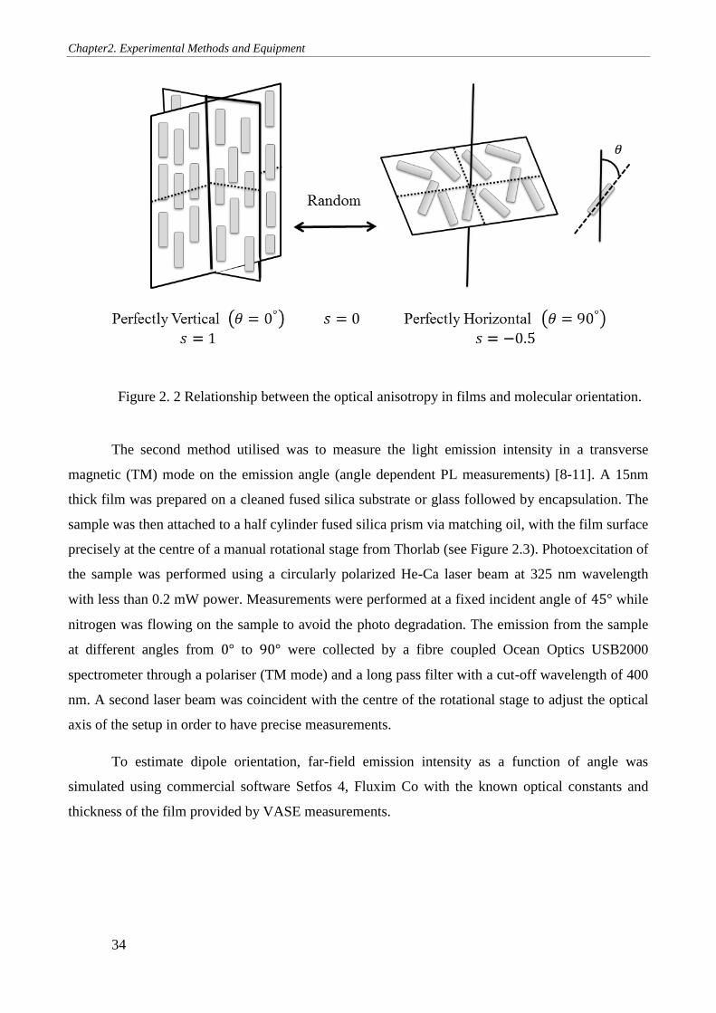
Chapter2. Experimental Methods and Equipment
34
Figure 2. 2 Relationship between the optical anisotropy in films and molecular orientation.
The second method utilised was to measure the light emission intensity in a transverse
magnetic (TM) mode on the emission angle (angle dependent PL measurements) [8-11]. A 15nm
thick film was prepared on a cleaned fused silica substrate or glass followed by encapsulation. The
sample was then attached to a half cylinder fused silica prism via matching oil, with the film surface
precisely at the centre of a manual rotational stage from Thorlab (see Figure 2.3). Photoexcitation of
the sample was performed using a circularly polarized He-Ca laser beam at 325 nm wavelength
with less than 0.2 mW power. Measurements were performed at a fixed incident angle of 45° while
nitrogen was flowing on the sample to avoid the photo degradation. The emission from the sample
at different angles from 0° to 90° were collected by a fibre coupled Ocean Optics USB2000
spectrometer through a polariser (TM mode) and a long pass filter with a cut-off wavelength of 400
nm. A second laser beam was coincident with the centre of the rotational stage to adjust the optical
axis of the setup in order to have precise measurements.
To estimate dipole orientation, far-field emission intensity as a function of angle was
simulated using commercial software Setfos 4, Fluxim Co with the known optical constants and
thickness of the film provided by VASE measurements.
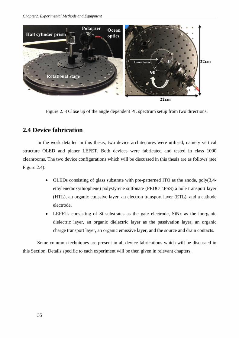
Chapter2. Experimental Methods and Equipment
35
Figure 2. 3 Close up of the angle dependent PL spectrum setup from two directions.
2.4 Device fabrication
In the work detailed in this thesis, two device architectures were utilised, namely vertical
structure OLED and planer LEFET. Both devices were fabricated and tested in class 1000
cleanrooms. The two device configurations which will be discussed in this thesis are as follows (see
Figure 2.4):
OLEDs consisting of glass substrate with pre-patterned ITO as the anode, poly(3,4-
ethylenedioxythiophene) polystyrene sulfonate (PEDOT:PSS) a hole transport layer
(HTL), an organic emissive layer, an electron transport layer (ETL), and a cathode
electrode.
LEFETs consisting of Si substrates as the gate electrode, SiNx as the inorganic
dielectric layer, an organic dielectric layer as the passivation layer, an organic
charge transport layer, an organic emissive layer, and the source and drain contacts.
Some common techniques are present in all device fabrications which will be discussed in
this Section. Details specific to each experiment will be then given in relevant chapters.
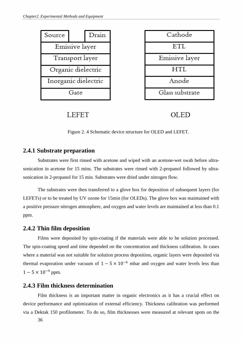
Chapter2. Experimental Methods and Equipment
36
Figure 2. 4 Schematic device structure for OLED and LEFET.
2.4.1 Substrate preparation
Substrates were first rinsed with acetone and wiped with an acetone-wet swab before ultra-
sonication in acetone for 15 mins. The substrates were rinsed with 2-propanol followed by ultra-
sonication in 2-propanol for 15 min. Substrates were dried under nitrogen flow.
The substrates were then transferred to a glove box for deposition of subsequent layers (for
LEFETs) or to be treated by UV ozone for 15min (for OLEDs). The glove box was maintained with
a positive pressure nitrogen atmosphere, and oxygen and water levels are maintained at less than 0.1
ppm.
2.4.2 Thin film deposition
Films were deposited by spin-coating if the materials were able to be solution processed.
The spin-coating speed and time depended on the concentration and thickness calibration. In cases
where a material was not suitable for solution process deposition, organic layers were deposited via
thermal evaporation under vacuum of 1 − 5 × 10⁻⁶ mbar and oxygen and water levels less than
1 − 5 × 10⁻⁹ ppm.
2.4.3 Film thickness determination
Film thickness is an important matter in organic electronics as it has a crucial effect on
device performance and optimization of external efficiency. Thickness calibration was performed
via a Dektak 150 profilometer. To do so, film thicknesses were measured at relevant spots on the
Chapter2. Experimental Methods and Equipment
37
substrate for five spots. Numbers were then averaged and used for calibration. In the case of thermal
deposition, a quartz crystal monitor was used during evaporation and then thickness was verified
using the Dektak profilometer.
2.4.4 Contact deposition
Cathode electrodes (in OLEDs) and source, drain electrodes (in LEFETs) were deposited via
shadow masks. Shadow masks were made from steel using laser cutting. Contacts were then
deposited through the shadow masks by thermal evaporation under a vacuum of 1 − 5 × 10⁻⁶
mbar.
2.5 Device characterisation
2.5.1 Standard measurements for light emission
For light emitting devices (OLEDs and LEFETs), the brightness and external quantum
efficiency must be determined in order to evaluate device performance. Since light emitting devices
are used mainly in display technology viewed by humans a measure of the human eye response
should be taken into account when describing their performances. Therefore, photometric units are
used to characterise light accounting for the sensitivity of the human eye [12]. However, physical
quantities of light such as number of photons, photon energy, or optical power are needed to be able
to determine EQE values. These quantities are radiometric units. Formal definitions of some of the
important photometric parameters for characterising light emitting devices are as follows:
Luminous intensity –light intensity of an optical source as observed by the human eye [12]
with unit measurements of candelas (cd). Candela is the light intensity of 1 standardised candle.
Candela –the candela is the luminous intensity, in a given direction, of a source that emits
monochromatic radiation of frequency 540 × 1012 Hz and that has a radiant intensity in that
direction of 1/683 watt per steradian [13].
Luminance or brightness –the ratio of luminous intensity emitted in specific direction
divided by the observed surface area in that direction, giving that light emitted in a solid angle from
the source, brightness is measured in cd/m2.
Luminous flux –the light power perceived by human eye from a source measured by unit
lumen (lm) [12].
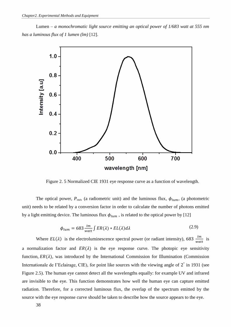
Chapter2. Experimental Methods and Equipment
38
Lumen – a monochromatic light source emitting an optical power of 1/683 watt at 555 nm
has a luminous flux of 1 lumen (lm) [12].
Figure 2. 5 Normalized CIE 1931 eye response curve as a function of wavelength.
The optical power, Pout, (a radiometric unit) and the luminous flux, 𝜙𝑙𝑢𝑚, (a photometric
unit) needs to be related by a conversion factor in order to calculate the number of photons emitted
by a light emitting device. The luminous flux 𝜙𝑙𝑢𝑚 , is related to the optical power by [12]
𝜙𝑙𝑢𝑚 = 683𝑙𝑚
𝑤𝑎𝑡𝑡∫ 𝐸𝑅(𝜆) ∗ 𝐸𝐿(𝜆)𝑑𝜆 (2.9)
Where 𝐸𝐿(𝜆) is the electroluminescence spectral power (or radiant intensity), 683 𝑙𝑚
𝑤𝑎𝑡𝑡 is
a normalization factor and 𝐸𝑅(𝜆) is the eye response curve. The photopic eye sensitivity
function, 𝐸𝑅(𝜆), was introduced by the International Commission for Illumination (Commission
Internationale de I’Eclairage, CIE), for point like sources with the viewing angle of 2° in 1931 (see
Figure 2.5). The human eye cannot detect all the wavelengths equally: for example UV and infrared
are invisible to the eye. This function demonstrates how well the human eye can capture emitted
radiation. Therefore, for a corrected luminous flux, the overlap of the spectrum emitted by the
source with the eye response curve should be taken to describe how the source appears to the eye.
Chapter2. Experimental Methods and Equipment
39
The total luminous flux 𝜙𝑙𝑢𝑚 leaving the device without being waveguided is given by
Greenham et.al [14]
𝜙𝑙𝑢𝑚 = ∫ 2𝜋𝐿
𝜋2
0
𝑐𝑜𝑠𝜃𝑠𝑖𝑛𝜃𝑑𝜃 (2.10)
Where 𝐿 is the flux per unit solid angle and 𝜃 is the angle from the normal which the light is
detected. Applying the trigonometric identity 𝑐𝑜𝑠𝜃𝑠𝑖𝑛𝜃 =1
2sin 2𝜃, Equation 2.10 becomes
𝜙𝑙𝑢𝑚 = ∫ 2𝜋𝐿
𝜋2
0
1
2𝑠𝑖𝑛2𝜃𝑑𝜃
𝜙𝑙𝑢𝑚 = 𝜋𝐿 [−1
2cos 2𝜃]
0
𝜋2
𝜙𝑙𝑢𝑚 = 𝜋𝐿
(2.11)
If 𝐿 is in cdm-2
unit, then
𝜙𝑙𝑢𝑚 = 𝜋𝐿 × 𝐴𝑒𝑚𝑖𝑠𝑠𝑖𝑜𝑛 (2.12)
Where 𝐴𝑒𝑚𝑖𝑠𝑠𝑖𝑜𝑛, is the area of light emission source, therefore 𝜙𝑙𝑢𝑚 will be in lumens (lm). For a
light emitting device, the luminous flux is given by Equation 2.9 while the optical power, Pout ,
emitted by a light source is given by an integration over all wavelengths by
𝑃𝑜𝑢𝑡 = ∫ 𝐸𝐿(𝜆)𝑑𝜆
(2.13)
The issue here is not having an absolute measurement of the radiant intensity. Available data is a
relative measurement of normalized 𝐸𝐿. However, the ratio of Equations 2.9 and 2.13 are valid and
is yield:
𝜙𝑙𝑢𝑚
𝑃𝑜𝑢𝑡= 683
𝑙𝑚
𝑤𝑎𝑡𝑡
∫ 𝐸𝑅(𝜆) ∗ 𝐸𝐿(𝜆)𝑑𝜆
∫ 𝐸𝐿(𝜆)𝑑𝜆
(2.14)
Using the Equation 2.12 , the optical power , 𝑃𝑜𝑢𝑡, is given by;
𝑃𝑜𝑢𝑡 =
𝐿 ∗ 𝜋 ∗ 𝐴𝑒𝑚𝑖𝑠𝑠𝑖𝑜𝑛
683𝑙𝑚
𝑤𝑎𝑡𝑡
∗∫ 𝐸𝐿(𝜆)𝑑𝜆
∫ 𝐸𝑅(𝜆) ∗ 𝐸𝐿(𝜆)𝑑𝜆
(2.15)
Chapter2. Experimental Methods and Equipment
40
The number of photons emitted by device is related to optical power by;
𝑃𝑜𝑢𝑡 = 𝑛𝑝ℎℎ𝜐 =
𝑛𝑝ℎℎ𝑐
𝜆
(2.16)
Where ℎ is Plank’s constant, 𝜐 is the frequency, 𝑛𝑝ℎ is the number of photons per unit time, 𝑐 is
the speed of light and 𝜆 is the wavelength. Instead of having a single wavelength, there are a range
of wavelengths for recorded radiant intensity. Therefore an average wavelength is needed as
follows:
𝜆𝑎𝑣 =
∫ 𝐸𝐿(𝜆)𝜆𝑑𝜆
∫ 𝐸𝐿(𝜆)𝑑𝜆
(2.17)
Substituting Equations 2.15 and 2.17 in 2.16 and rearranging:
𝑛𝑝ℎ =
𝐿 ∗ 𝜋 ∗ 𝐴𝑒𝑚𝑖𝑠𝑠𝑖𝑜𝑛
683𝑙𝑚
𝑤𝑎𝑡𝑡
∗∫ 𝐸𝐿(𝜆)𝜆𝑑𝜆
∫ 𝐸𝑅(𝜆) ∗ 𝐸𝐿(𝜆)𝑑𝜆
(2.18)
The number of electrons per second injected into the device, 𝑛𝑒 is given by:
𝑛𝑒 =
𝐼
𝑒
(2.19)
Where 𝑒 is charge for an electron 1.6 × 10⁻¹⁹ 𝑐 and I is current (A). The EQE can then be found as
the ratio of photons per second emitted by device in the viewing direction to the number of injected
electrons per second to the device:
𝐸𝑄𝐸 =𝑛𝑝ℎ
𝑛𝑒
(2.20)
2.5.2 Colourimetry
The emitted “colour” of our devices is described by colour-matching functions and a
chromaticity diagram by the CIE. Figure 2.6.a shows the three colour-matching functions, �̅�(𝜆),
�̅�(𝜆), and 𝑧̅(𝜆) which represent red, green and blue light respectively. These functions are
dimensionless and result from the colour of light being described using these three variables. For a
given colour spectral density, 𝑃𝑠𝑝𝑒𝑐𝑡𝑟𝑢𝑚(𝜆), the overlap of the spectral density with each of the
colour-matching functions gives the degree of each function required to match the colour of the
spectrum as follows:
𝑋 = ∫ �̅�(𝜆) 𝑃𝑠𝑝𝑒𝑐𝑡𝑟𝑢𝑚(𝜆)𝑑𝜆
(2.21)
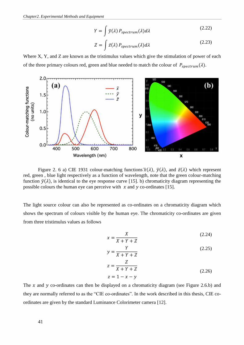
Chapter2. Experimental Methods and Equipment
41
𝑌 = ∫ �̅�(𝜆) 𝑃𝑠𝑝𝑒𝑐𝑡𝑟𝑢𝑚(𝜆)𝑑𝜆
(2.22)
𝑍 = ∫ 𝑧̅(𝜆) 𝑃𝑠𝑝𝑒𝑐𝑡𝑟𝑢𝑚(𝜆)𝑑𝜆
(2.23)
Where X, Y, and Z are known as the tristimulus values which give the stimulation of power of each
of the three primary colours red, green and blue needed to match the colour of 𝑃𝑠𝑝𝑒𝑐𝑡𝑟𝑢𝑚(𝜆).
Figure 2. 6 a) CIE 1931 colour-matching functions �̅�(𝜆), �̅�(𝜆), and 𝑧̅(𝜆) which represent
red, green , blue light respectively as a function of wavelength, note that the green colour-matching
function �̅�(𝜆), is identical to the eye response curve [15]. b) chromaticity diagram representing the
possible colours the human eye can perceive with 𝑥 and 𝑦 co-ordinates [15].
The light source colour can also be represented as co-ordinates on a chromaticity diagram which
shows the spectrum of colours visible by the human eye. The chromaticity co-ordinates are given
from three tristimulus values as follows
𝑥 =
𝑋
𝑋 + 𝑌 + 𝑍
(2.24)
𝑦 =
𝑌
𝑋 + 𝑌 + 𝑍
(2.25)
𝑧 =
𝑍
𝑋 + 𝑌 + 𝑍
𝑧 = 1 − 𝑥 − 𝑦
(2.26)
The 𝑥 and 𝑦 co-ordinates can then be displayed on a chromaticity diagram (see Figure 2.6.b) and
they are normally referred to as the “CIE co-ordinates”. In the work described in this thesis, CIE co-
ordinates are given by the standard Luminance Colorimeter camera [12].
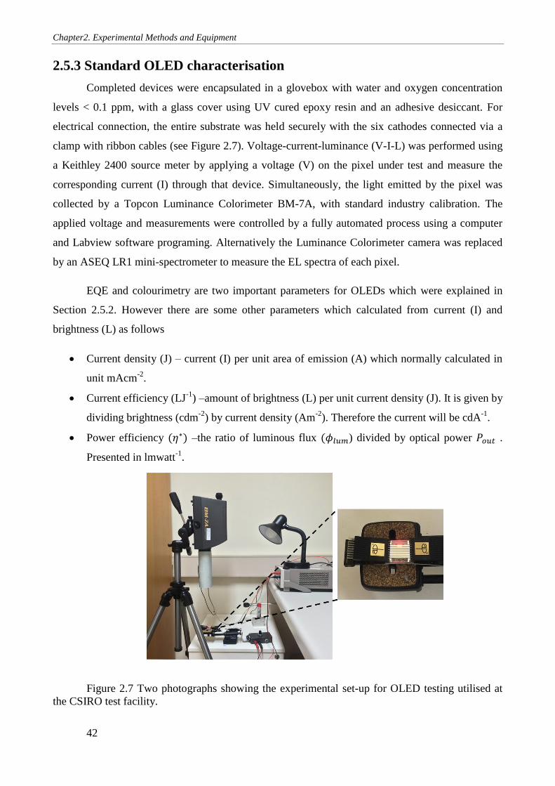
Chapter2. Experimental Methods and Equipment
42
2.5.3 Standard OLED characterisation
Completed devices were encapsulated in a glovebox with water and oxygen concentration
levels < 0.1 ppm, with a glass cover using UV cured epoxy resin and an adhesive desiccant. For
electrical connection, the entire substrate was held securely with the six cathodes connected via a
clamp with ribbon cables (see Figure 2.7). Voltage-current-luminance (V-I-L) was performed using
a Keithley 2400 source meter by applying a voltage (V) on the pixel under test and measure the
corresponding current (I) through that device. Simultaneously, the light emitted by the pixel was
collected by a Topcon Luminance Colorimeter BM-7A, with standard industry calibration. The
applied voltage and measurements were controlled by a fully automated process using a computer
and Labview software programing. Alternatively the Luminance Colorimeter camera was replaced
by an ASEQ LR1 mini-spectrometer to measure the EL spectra of each pixel.
EQE and colourimetry are two important parameters for OLEDs which were explained in
Section 2.5.2. However there are some other parameters which calculated from current (I) and
brightness (L) as follows
Current density (J) – current (I) per unit area of emission (A) which normally calculated in
unit mAcm-2
.
Current efficiency (LJ-1
) –amount of brightness (L) per unit current density (J). It is given by
dividing brightness (cdm-2
) by current density (Am-2
). Therefore the current will be cdA-1
.
Power efficiency (𝜂∗) –the ratio of luminous flux (𝜙𝑙𝑢𝑚) divided by optical power 𝑃𝑜𝑢𝑡 .
Presented in lmwatt-1
.
Figure 2.7 Two photographs showing the experimental set-up for OLED testing utilised at
the CSIRO test facility.
Chapter2. Experimental Methods and Equipment
43
2.5.4 Standard LEFET characterisation
Completed LEFET devices were encapsulated with a thick layer of Cytop, CTL-809 M
(solvent: CTSolv.180) from Asahi Glass Japan. They were then transferred to the testing glove box
where electrical and optical characterisation was performed using an Agilent B1500A
Semiconductor Analyser on a SA-6 Semi-Automatic Probe Station. The light output from devices
was simultaneously measured during operation by a calibrated photomultiplier tube (PMT), a
Hamamatsu H10721-20, positioned directly over the device with a fixed distance (see Figure 2.8).
The PMT and the three probes were individually connected electrically to the Agilent which was
positioned outside the glove box. The source-drain current of the LEFET and photocurrent from
PMT were recorded for electrical and optical characterisation.
2.5.4.1 Optical characterisation
In order to convert the PMT photocurrent to brightness the PMT was calibrated using an
OLED fabricated by commercially available emissive layer super yellow. The reason for choosing
an OLED is the easier encapsulation process and possibility for brightness measurements with
luminance meter outside the glove box. The performance of the encapsulate OLED was then
measured at different applied voltages once with luminance meter (Konica Minolta LS100) and
again with PMT fixed for certain distance and gain. The PMT photocurrent as a function of
brightness were then plotted in order to calibrate the PMT. The slope of the calibration curve was
then used to find the brightness of a device with known PMT current. At fixed gain of 0.4 and for
OLED area of 0.92 mm2 the slope of the calibration is 69.0 𝑛𝐴 𝑐𝑑 𝑚−2 and so;
1𝑐𝑑 𝑚−2 ≈ 69.0 𝑛𝐴 (2.27)
The calibration can be adjusted for the difference in emission area of the LEFET and OLED as;
1𝑐𝑑 𝑚−2 ≈ 69.0 𝑛𝐴 ×
𝐴𝑟𝑒𝑎𝑒𝑚𝑖𝑠𝑠𝑖𝑜𝑛(𝐿𝐸𝐹𝐸𝑇)
𝐴𝑟𝑒𝑎𝑒𝑚𝑖𝑠𝑠𝑖𝑜𝑛(𝑂𝐿𝐸𝐷)
(2.28)
The conversion between PMT current in 𝑛𝐴 and brightness (L) in 𝑐𝑑 𝑚−2 is then;
𝐿 (𝑐𝑑 𝑚−2) = 𝑃𝑀𝑇 𝑐𝑢𝑟𝑟𝑒𝑛𝑡 (𝑛𝐴) ×
𝐴𝑟𝑒𝑎𝑒𝑚𝑖𝑠𝑠𝑖𝑜𝑛(𝐿𝐸𝐹𝐸𝑇)
𝐴𝑟𝑒𝑎𝑒𝑚𝑖𝑠𝑠𝑖𝑜𝑛(𝑂𝐿𝐸𝐷)×
1
69.0 𝑛𝐴 𝑐𝑑 𝑚−2
(2.29)
The EQE can then be determined as explained in Section 2.5.1.
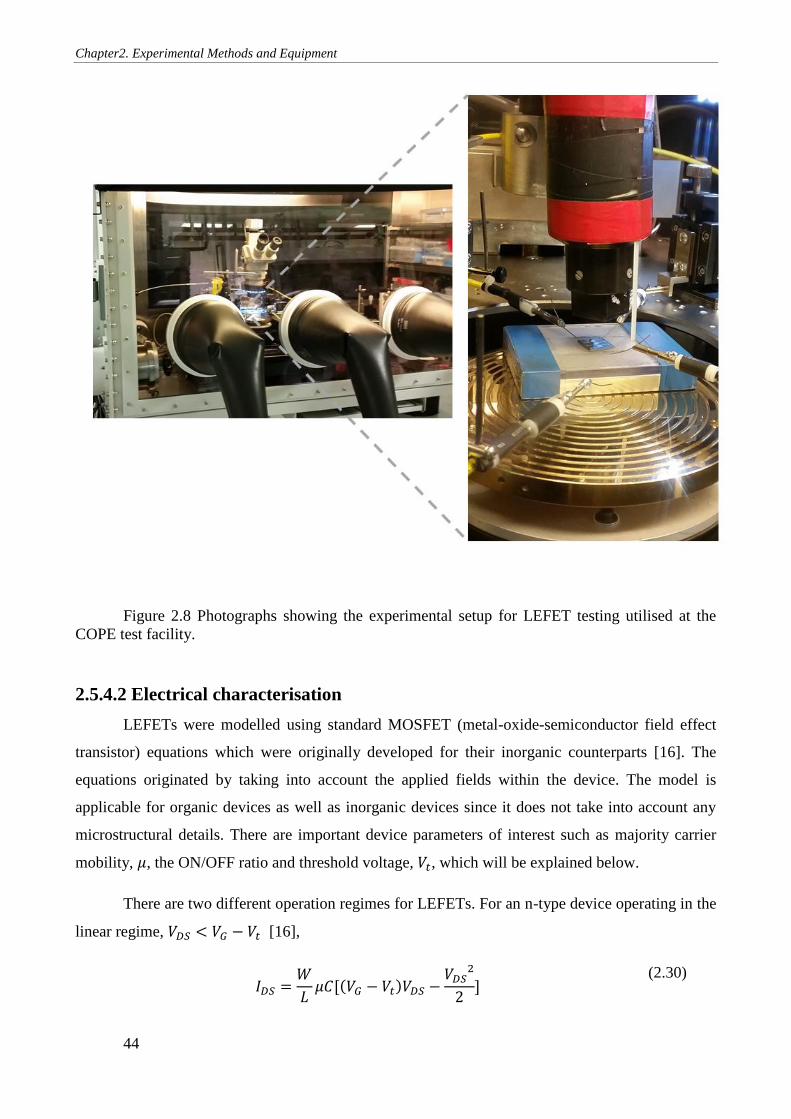
Chapter2. Experimental Methods and Equipment
44
Figure 2.8 Photographs showing the experimental setup for LEFET testing utilised at the
COPE test facility.
2.5.4.2 Electrical characterisation
LEFETs were modelled using standard MOSFET (metal-oxide-semiconductor field effect
transistor) equations which were originally developed for their inorganic counterparts [16]. The
equations originated by taking into account the applied fields within the device. The model is
applicable for organic devices as well as inorganic devices since it does not take into account any
microstructural details. There are important device parameters of interest such as majority carrier
mobility, 𝜇, the ON/OFF ratio and threshold voltage, 𝑉𝑡, which will be explained below.
There are two different operation regimes for LEFETs. For an n-type device operating in the
linear regime, 𝑉𝐷𝑆 < 𝑉𝐺 − 𝑉𝑡 [16],
𝐼𝐷𝑆 =
𝑊
𝐿𝜇𝐶[(𝑉𝐺 − 𝑉𝑡)𝑉𝐷𝑆 −
𝑉𝐷𝑆2
2]
(2.30)
Chapter2. Experimental Methods and Equipment
45
where 𝐼𝐷𝑆 is the source-drain current, 𝑊 and 𝐿 are the length and width of the transistor channel
respectively and 𝐶 is the capacitance of the dielectric layer which can be determined by a series of
organic and inorganic dielectric layers. In the saturation regime, where 𝑉𝐷𝑆 ≥ 𝑉𝐺 − 𝑉𝑡 [16],
𝐼𝐷𝑆 =
𝑊
𝐿
𝜇𝐶
2(𝑉𝐺 − 𝑉𝑡)2
(2.31)
These equations can be used for p-type devices with a sign difference respective of the opposite
polarity of the applied voltages. In the work details in this thesis, the LEFET mobility was
determined from the transfer characteristics in the saturation regime. In a small threshold voltage,
the mobility in the saturation regime is given by
𝜇 =2𝐿
𝑊𝐶(
√𝜕𝐼𝐷𝑆
𝜕𝑉𝐺)
2
(2.32)
The threshold voltage, which is the minimum gate voltage that must be applied to switch the device
ON, can be determined by finding the 𝑥 intercept of the √𝐼𝐷𝑆 vs 𝑉𝐺 plot.
The ON/OFF ratio is a parameter which shows the switching capability of a LEFET. It is the ratio
between the maximum current measured when the device is switched ON and the minimum current
of the transfer characteristics.
In this chapter, the methodologies and basic principles for characterising OLED and LEFET
materials and devices were described. In particular, dendritic phosphorescent materials suitable for
OLEDs, where appropriate additional experimental and theoretical details will be provided in
subsequent Sections. In the next chapter, the first of the results will be described concerning a
systematic study of a basic dendritic dendrimer structure consisting of Iridium complex with
biphenyl dendron.
Chapter2. Experimental Methods and Equipment
46
References
[1] J. Li, Y. Zhao, H.S. Tan, Y. Guo, C.-A. Di, G. Yu, Y. Liu, M. Lin, S.H. Lim, Y. Zhou, A stable
solution-processed polymer semiconductor with record high-mobility for printed transistors,
Scientific reports, 2 (2012).
[2] R. Joseph, Lakowicz. Principles of fluorescence spectroscopy, in, Springer, 2006.
[3] G.A. Crosby, J.N. Demas, Measurement of photoluminescence quantum yields. Review, The
Journal of Physical Chemistry, 75 (1971) 991-1024.
[4] N. Greenham, I. Samuel, G. Hayes, R. Phillips, Y. Kessener, S. Moratti, A. Holmes, R. Friend,
Measurement of absolute photoluminescence quantum efficiencies in conjugated polymers,
Chemical physics letters, 241 (1995) 89-96.
[5] P.E. Shaw, Measurements of exciton diffusion in conjugated polymers, in, University of St
Andrews, 2009.
[6] J. Woollam, Guide to using WVASE32 JA Woollam co, in, Inc, 2002.
[7] D. Yokoyama, Molecular orientation in small-molecule organic light-emitting diodes, Journal of
Materials Chemistry, 21 (2011) 19187-19202.
[8] W. Brütting, J. Frischeisen, T.D. Schmidt, B.J. Scholz, C. Mayr, Device efficiency of organic
light‐emitting diodes: Progress by improved light outcoupling, physica status solidi (a), 210 (2013)
44-65.
[9] K.H. Kim, C.K. Moon, J.H. Lee, S.Y. Kim, J.J. Kim, Highly Efficient Organic Light‐Emitting
Diodes with Phosphorescent Emitters Having High Quantum Yield and Horizontal Orientation of
Transition Dipole Moments, Advanced Materials, 26 (2014) 3844-3847.
[10] L. Zhao, T. Komino, M. Inoue, J.-H. Kim, J.C. Ribierre, C. Adachi, Horizontal molecular
orientation in solution-processed organic light-emitting diodes, Applied Physics Letters, 106 (2015)
063301.
[11] M.J. Jurow, C. Mayr, T.D. Schmidt, T. Lampe, P.I. Djurovich, W. Brütting, M.E. Thompson,
Understanding and predicting the orientation of heteroleptic phosphors in organic light-emitting
materials, Nature materials, (2015).
[12] E.F. Schubert, Light-Emitting Diodes (2006), E. Fred Schubert, 2006.
[13] Bureau International des Poids et Mesures. The International System of Units (SI), 8thEdition
(Organisation Intergouvernementale de la Convention du Mètre, 2006), in.
[14] N.C. Greenham, R.H. Friend, D.D. Bradley, Angular Dependence of the Emission from a
Conjugated Polymer Light‐Emitting Diode: Implications for efficiency calculations, Advanced
Materials, 6 (1994) 491-494.
[15] K. Tandy, Active channel field-effect transistors: Towards high performance light emitting
transistors, (2014).
[16] Z. Bao, J. Locklin, Organic field-effect transistors, CRC press, 2007.
47
Chapter 3
Highly Efficient Solution-Processable
Dendrimer OLEDs
3.1 Introduction
The development of organic semiconductors in last three decades is widely viewed as the
next technology wave in optoelectronics, and it is one of the most exciting fields of research not
only in science but also industry. The ability of organic semiconductors to combine tunable
optoelectronic properties with the desire for much simpler processing compared to their inorganic
counterparts has made them formidable competitors in the market. Over the past decade, organic
light emitting diodes became a promising candidate for flat panel display technology due to their
high efficiency, low driving voltage, light weight, and low cost of both materials and processing.
Among all materials investigated in OLEDs, phosphorescent materials have gained specific
attention due to their potential for 100% internal quantum efficiency by harvesting both singlet and
triplet excitons [1-3]. So far, iridium (III) complexes have been the most promising candidates,
offering high efficiency, relatively short excited state lifetimes, and colour tunability [4-9]. Iridium
(III) complexes have been demonstrated in the three different categories of small molecules [10,
11], polymers [12-14] and dendritic architectures [15-18]. Devices based on small molecules have
shown less potential due to the need for high temperature high vacuum deposition techniques.
Although polymers are promising with highly cost effective processing techniques such as spin
coating and inkjet printing [19], any attempts to tune processing often leads to undesirable changes
in the electronic and emissive properties of the resultant devices. Using dendritic structures allows
independent control over intermolecular interactions as well as emissive properties. There have
been several reports on phosphorescent dendrimer OLEDs in the last decade [15-18, 20-23]. It is
important to simplify fabrication, in line with the desire for mass production large area displays.
Previous attempts to make efficient OLEDs out of neat film Ir(III) core complexes have shown
poor efficiencies due to the strong interaction between chromophores which led to quenching the
luminescence [24].
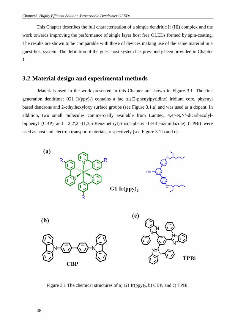
Chapter3. Highly Efficient Solution-Processable Dendrimer OLEDs
48
This Chapter describes the full characterisation of a simple dendritic Ir (III) complex and the
work towards improving the performance of single layer host free OLEDs formed by spin-coating.
The results are shown to be comparable with those of devices making use of the same material in a
guest-host system. The definition of the guest-host system has previously been provided in Chapter
1.
3.2 Material design and experimental methods
Materials used in the work presented in this Chapter are shown in Figure 3.1. The first
generation dendrimer (G1 Ir(ppy)3) contains a fac tris(2-phenylpyridine) iridium core, phyenyl
based dendrons and 2-ethylhexyloxy surface groups (see Figure 3.1.a) and was used as a dopant. In
addition, two small molecules commercially available from Lumtec, 4,4’-N,N’-dicarbazolyl-
biphenyl (CBP) and 2,2',2"-(1,3,5-Benzinetriyl)-tris(1-phenyl-1-H-benzimidazole) (TPBi) were
used as host and electron transport materials, respectively (see Figure 3.1.b and c).
Figure 3.1 The chemical structures of a) G1 Ir(ppy)3, b) CBP, and c) TPBi.
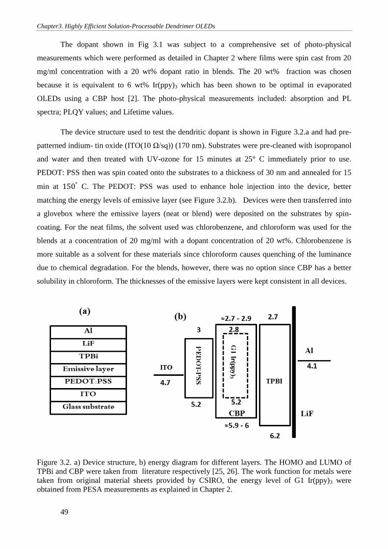
Chapter3. Highly Efficient Solution-Processable Dendrimer OLEDs
49
The dopant shown in Fig 3.1 was subject to a comprehensive set of photo-physical
measurements which were performed as detailed in Chapter 2 where films were spin cast from 20
mg/ml concentration with a 20 wt% dopant ratio in blends. The 20 wt% fraction was chosen
because it is equivalent to 6 wt% Ir(ppy)3 which has been shown to be optimal in evaporated
OLEDs using a CBP host [2]. The photo-physical measurements included: absorption and PL
spectra; PLQY values; and Lifetime values.
The device structure used to test the dendritic dopant is shown in Figure 3.2.a and had pre-
patterned indium- tin oxide (ITO(10 Ω/sq)) (170 nm). Substrates were pre-cleaned with isopropanol
and water and then treated with UV-ozone for 15 minutes at 25° C immediately prior to use.
PEDOT: PSS then was spin coated onto the substrates to a thickness of 30 nm and annealed for 15
min at 150° C. The PEDOT: PSS was used to enhance hole injection into the device, better
matching the energy levels of emissive layer (see Figure 3.2.b). Devices were then transferred into
a glovebox where the emissive layers (neat or blend) were deposited on the substrates by spin-
coating. For the neat films, the solvent used was chlorobenzene, and chloroform was used for the
blends at a concentration of 20 mg/ml with a dopant concentration of 20 wt%. Chlorobenzene is
more suitable as a solvent for these materials since chloroform causes quenching of the luminance
due to chemical degradation. For the blends, however, there was no option since CBP has a better
solubility in chloroform. The thicknesses of the emissive layers were kept consistent in all devices.
Figure 3.2. a) Device structure, b) energy diagram for different layers. The HOMO and LUMO of
TPBi and CBP were taken from literature respectively [25, 26]. The work function for metals were
taken from original material sheets provided by CSIRO, the energy level of G1 Ir(ppy)3 were
obtained from PESA measurements as explained in Chapter 2.
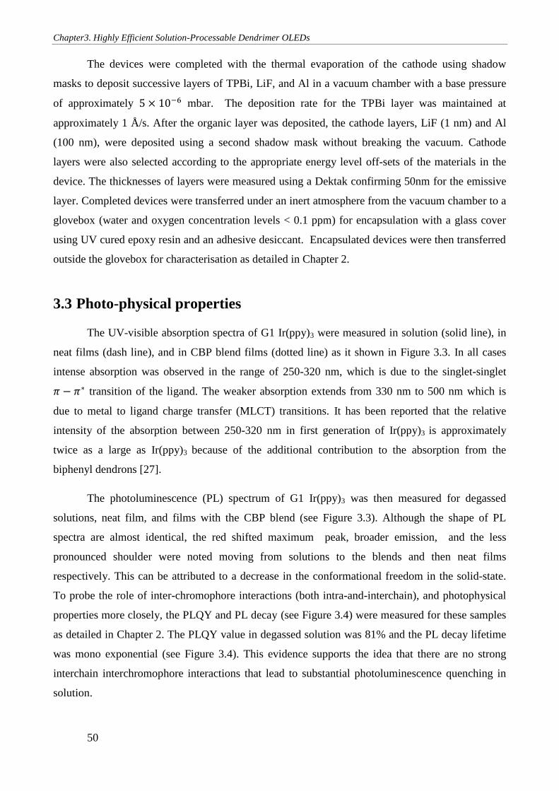
Chapter3. Highly Efficient Solution-Processable Dendrimer OLEDs
50
The devices were completed with the thermal evaporation of the cathode using shadow
masks to deposit successive layers of TPBi, LiF, and Al in a vacuum chamber with a base pressure
of approximately 5 × 10⁻⁶ mbar. The deposition rate for the TPBi layer was maintained at
approximately 1 Å/s. After the organic layer was deposited, the cathode layers, LiF (1 nm) and Al
(100 nm), were deposited using a second shadow mask without breaking the vacuum. Cathode
layers were also selected according to the appropriate energy level off-sets of the materials in the
device. The thicknesses of layers were measured using a Dektak confirming 50nm for the emissive
layer. Completed devices were transferred under an inert atmosphere from the vacuum chamber to a
glovebox (water and oxygen concentration levels < 0.1 ppm) for encapsulation with a glass cover
using UV cured epoxy resin and an adhesive desiccant. Encapsulated devices were then transferred
outside the glovebox for characterisation as detailed in Chapter 2.
3.3 Photo-physical properties
The UV-visible absorption spectra of G1 Ir(ppy)3 were measured in solution (solid line), in
neat films (dash line), and in CBP blend films (dotted line) as it shown in Figure 3.3. In all cases
intense absorption was observed in the range of 250-320 nm, which is due to the singlet-singlet
𝜋 − 𝜋∗ transition of the ligand. The weaker absorption extends from 330 nm to 500 nm which is
due to metal to ligand charge transfer (MLCT) transitions. It has been reported that the relative
intensity of the absorption between 250-320 nm in first generation of Ir(ppy)3 is approximately
twice as a large as Ir(ppy)3 because of the additional contribution to the absorption from the
biphenyl dendrons [27].
The photoluminescence (PL) spectrum of G1 Ir(ppy)3 was then measured for degassed
solutions, neat film, and films with the CBP blend (see Figure 3.3). Although the shape of PL
spectra are almost identical, the red shifted maximum peak, broader emission, and the less
pronounced shoulder were noted moving from solutions to the blends and then neat films
respectively. This can be attributed to a decrease in the conformational freedom in the solid-state.
To probe the role of inter-chromophore interactions (both intra-and-interchain), and photophysical
properties more closely, the PLQY and PL decay (see Figure 3.4) were measured for these samples
as detailed in Chapter 2. The PLQY value in degassed solution was 81% and the PL decay lifetime
was mono exponential (see Figure 3.4). This evidence supports the idea that there are no strong
interchain interchromophore interactions that lead to substantial photoluminescence quenching in
solution.
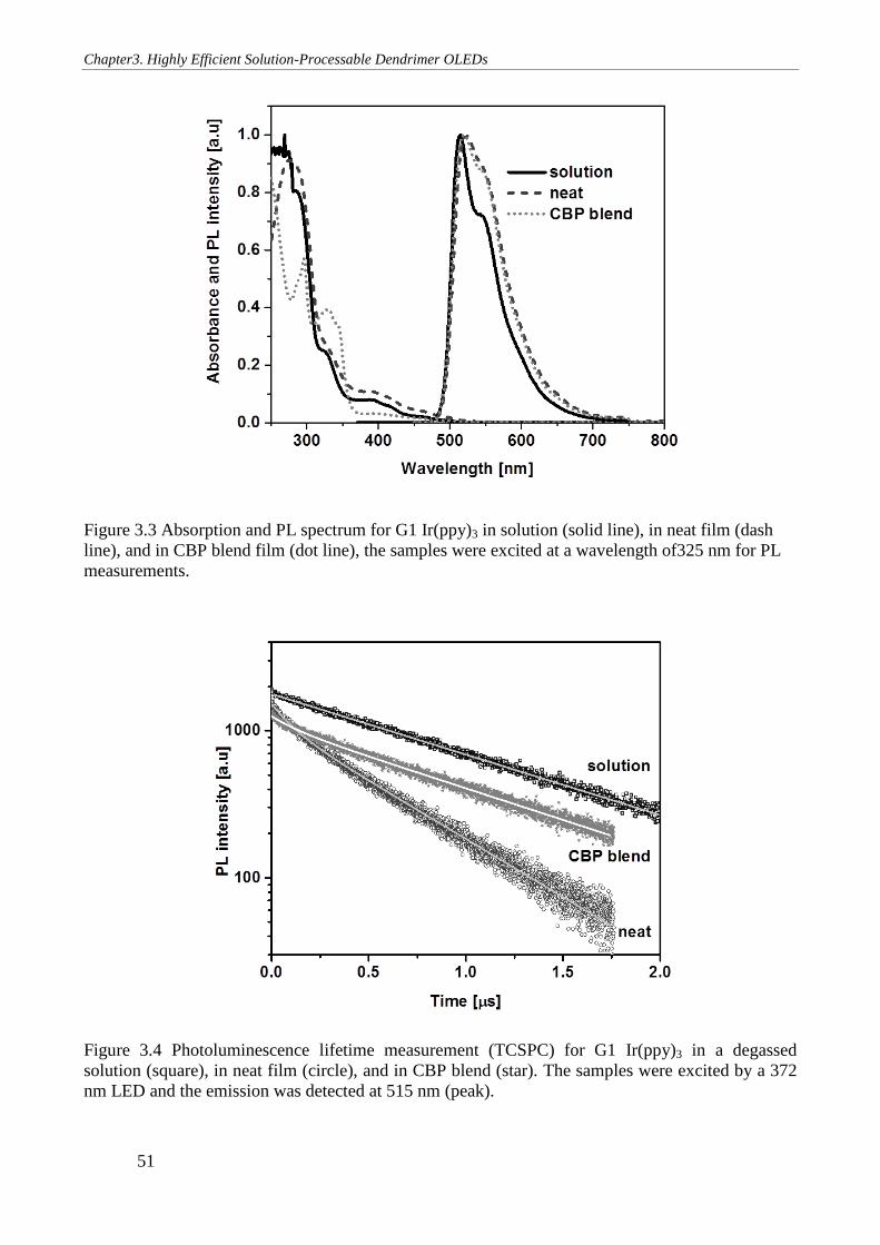
Chapter3. Highly Efficient Solution-Processable Dendrimer OLEDs
51
Figure 3.3 Absorption and PL spectrum for G1 Ir(ppy)3 in solution (solid line), in neat film (dash
line), and in CBP blend film (dot line), the samples were excited at a wavelength of325 nm for PL
measurements.
Figure 3.4 Photoluminescence lifetime measurement (TCSPC) for G1 Ir(ppy)3 in a degassed
solution (square), in neat film (circle), and in CBP blend (star). The samples were excited by a 372
nm LED and the emission was detected at 515 nm (peak).
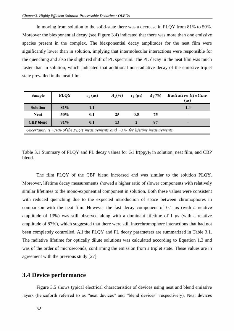
Chapter3. Highly Efficient Solution-Processable Dendrimer OLEDs
52
In moving from solution to the solid-state there was a decrease in PLQY from 81% to 50%.
Moreover the biexponential decay (see Figure 3.4) indicated that there was more than one emissive
species present in the complex. The biexponential decay amplitudes for the neat film were
significantly lower than in solution, implying that intermolecular interactions were responsible for
the quenching and also the slight red shift of PL spectrum. The PL decay in the neat film was much
faster than in solution, which indicated that additional non-radiative decay of the emissive triplet
state prevailed in the neat film.
Table 3.1 Summary of PLQY and PL decay values for G1 Ir(ppy)3 in solution, neat film, and CBP
blend.
The film PLQY of the CBP blend increased and was similar to the solution PLQY.
Moreover, lifetime decay measurements showed a higher ratio of slower components with relatively
similar lifetimes to the mono-exponential component in solution. Both these values were consistent
with reduced quenching due to the expected introduction of space between chromophores in
comparison with the neat film. However the fast decay component of 0.1 μs (with a relative
amplitude of 13%) was still observed along with a dominant lifetime of 1 μs (with a relative
amplitude of 87%), which suggested that there were still interchromophore interactions that had not
been completely controlled. All the PLQY and PL decay parameters are summarized in Table 3.1.
The radiative lifetime for optically dilute solutions was calculated according to Equation 1.3 and
was of the order of microseconds, confirming the emission from a triplet state. These values are in
agreement with the previous study [27].
3.4 Device performance
Figure 3.5 shows typical electrical characteristics of devices using neat and blend emissive
layers (henceforth referred to as “neat devices” and “blend devices” respectively). Neat devices
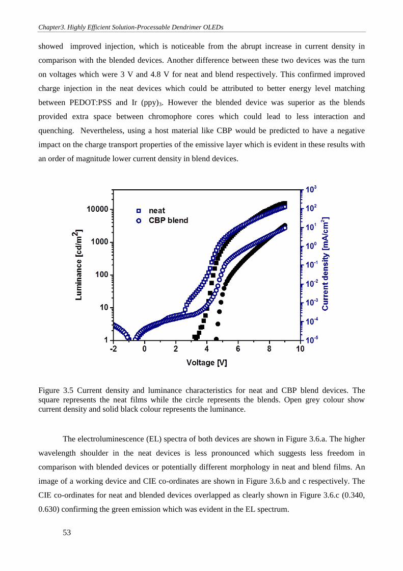
Chapter3. Highly Efficient Solution-Processable Dendrimer OLEDs
53
showed improved injection, which is noticeable from the abrupt increase in current density in
comparison with the blended devices. Another difference between these two devices was the turn
on voltages which were 3 V and 4.8 V for neat and blend respectively. This confirmed improved
charge injection in the neat devices which could be attributed to better energy level matching
between PEDOT:PSS and Ir (ppy)3. However the blended device was superior as the blends
provided extra space between chromophore cores which could lead to less interaction and
quenching. Nevertheless, using a host material like CBP would be predicted to have a negative
impact on the charge transport properties of the emissive layer which is evident in these results with
an order of magnitude lower current density in blend devices.
Figure 3.5 Current density and luminance characteristics for neat and CBP blend devices. The
square represents the neat films while the circle represents the blends. Open grey colour show
current density and solid black colour represents the luminance.
The electroluminescence (EL) spectra of both devices are shown in Figure 3.6.a. The higher
wavelength shoulder in the neat devices is less pronounced which suggests less freedom in
comparison with blended devices or potentially different morphology in neat and blend films. An
image of a working device and CIE co-ordinates are shown in Figure 3.6.b and c respectively. The
CIE co-ordinates for neat and blended devices overlapped as clearly shown in Figure 3.6.c (0.340,
0.630) confirming the green emission which was evident in the EL spectrum.
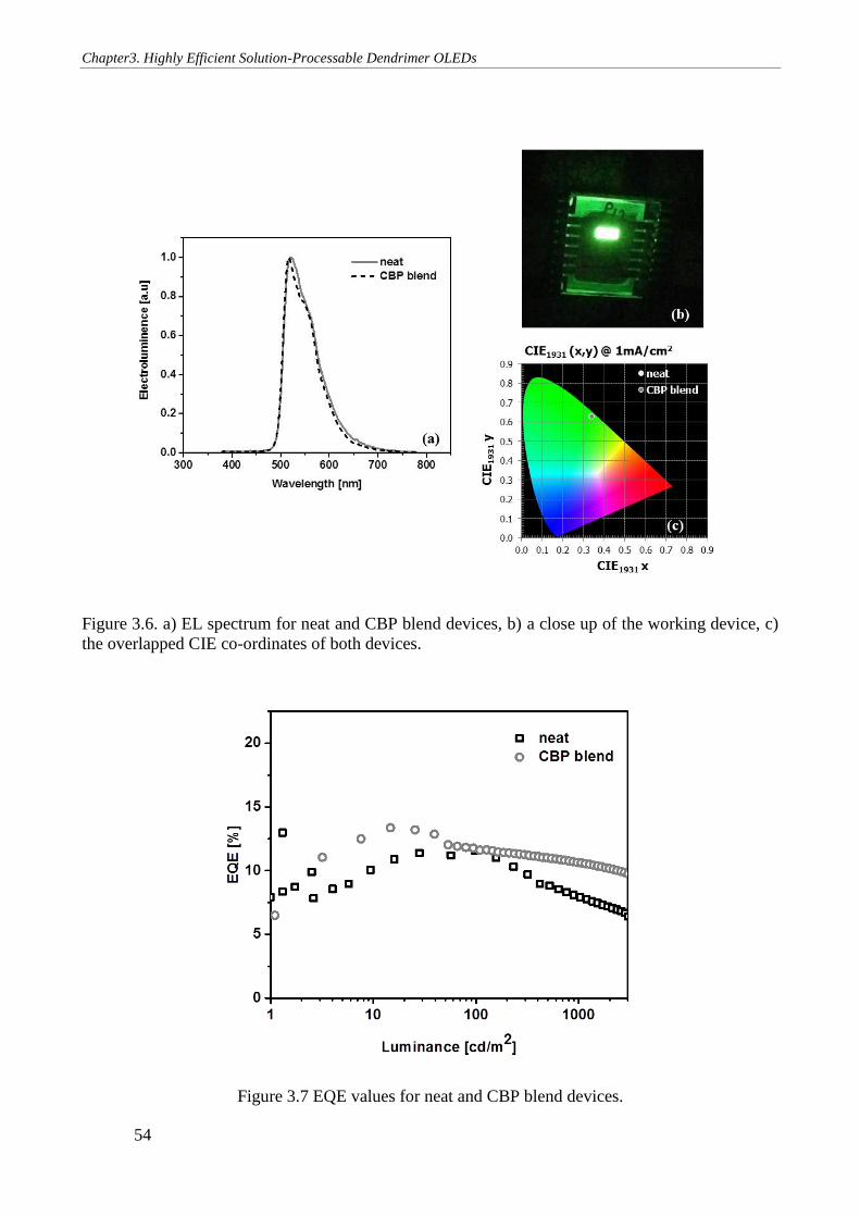
Chapter3. Highly Efficient Solution-Processable Dendrimer OLEDs
54
Figure 3.6. a) EL spectrum for neat and CBP blend devices, b) a close up of the working device, c)
the overlapped CIE co-ordinates of both devices.
Figure 3.7 EQE values for neat and CBP blend devices.
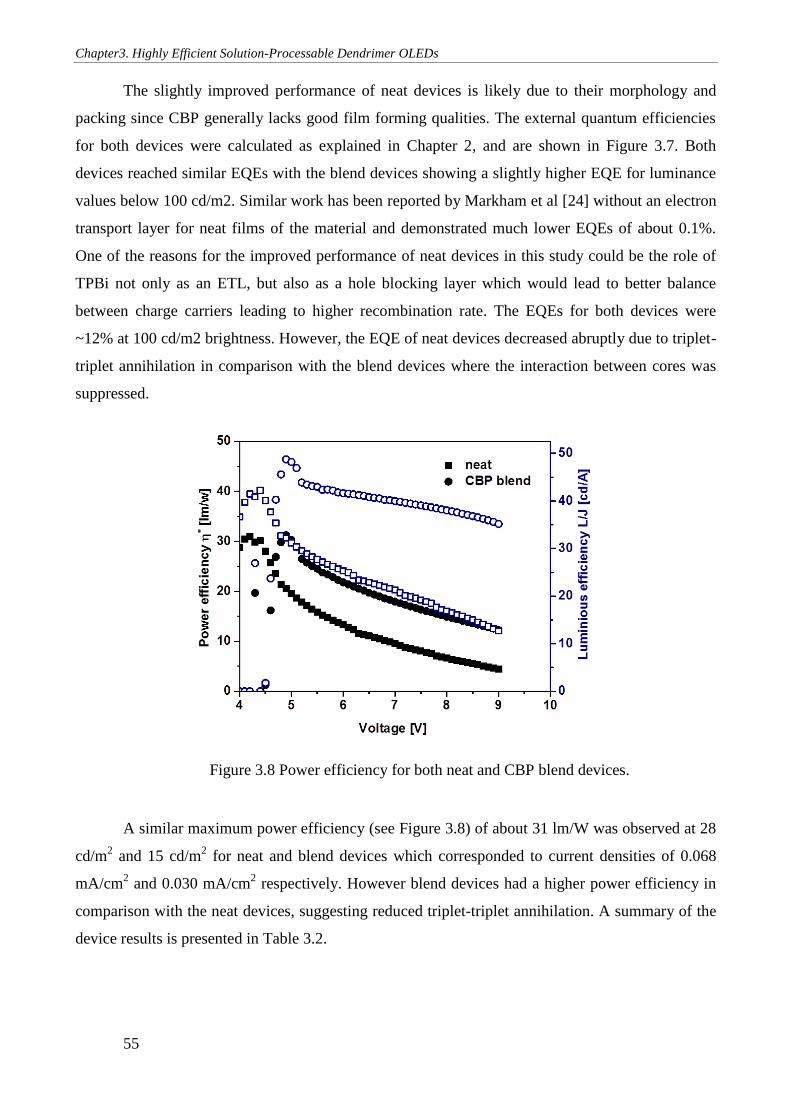
Chapter3. Highly Efficient Solution-Processable Dendrimer OLEDs
55
The slightly improved performance of neat devices is likely due to their morphology and
packing since CBP generally lacks good film forming qualities. The external quantum efficiencies
for both devices were calculated as explained in Chapter 2, and are shown in Figure 3.7. Both
devices reached similar EQEs with the blend devices showing a slightly higher EQE for luminance
values below 100 cd/m2. Similar work has been reported by Markham et al [24] without an electron
transport layer for neat films of the material and demonstrated much lower EQEs of about 0.1%.
One of the reasons for the improved performance of neat devices in this study could be the role of
TPBi not only as an ETL, but also as a hole blocking layer which would lead to better balance
between charge carriers leading to higher recombination rate. The EQEs for both devices were
~12% at 100 cd/m2 brightness. However, the EQE of neat devices decreased abruptly due to triplet-
triplet annihilation in comparison with the blend devices where the interaction between cores was
suppressed.
Figure 3.8 Power efficiency for both neat and CBP blend devices.
A similar maximum power efficiency (see Figure 3.8) of about 31 lm/W was observed at 28
cd/m2 and 15 cd/m
2 for neat and blend devices which corresponded to current densities of 0.068
mA/cm2 and 0.030 mA/cm
2 respectively. However blend devices had a higher power efficiency in
comparison with the neat devices, suggesting reduced triplet-triplet annihilation. A summary of the
device results is presented in Table 3.2.
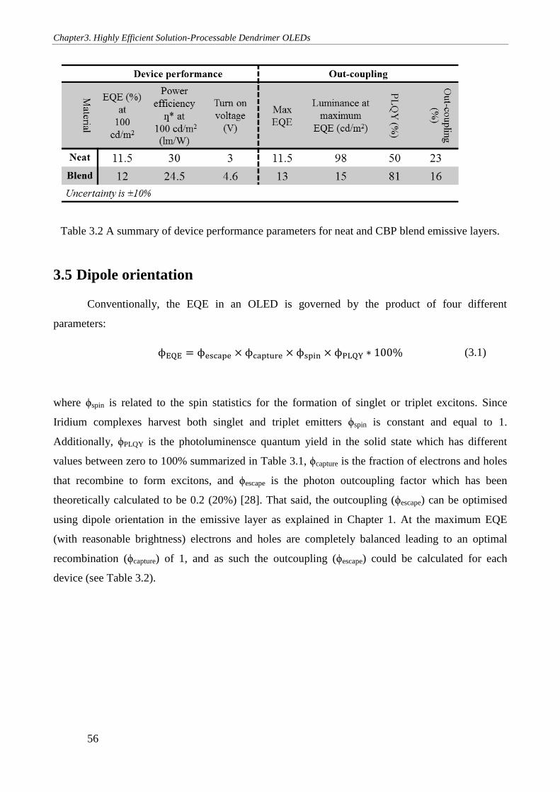
Chapter3. Highly Efficient Solution-Processable Dendrimer OLEDs
56
Table 3.2 A summary of device performance parameters for neat and CBP blend emissive layers.
3.5 Dipole orientation
Conventionally, the EQE in an OLED is governed by the product of four different
parameters:
ϕEQE = ϕescape × ϕcapture × ϕspin × ϕPLQY ∗ 100% (3.1)
where ϕspin is related to the spin statistics for the formation of singlet or triplet excitons. Since
Iridium complexes harvest both singlet and triplet emitters ϕspin is constant and equal to 1.
Additionally, ϕPLQY is the photoluminensce quantum yield in the solid state which has different
values between zero to 100% summarized in Table 3.1, ϕcapture is the fraction of electrons and holes
that recombine to form excitons, and ϕescape is the photon outcoupling factor which has been
theoretically calculated to be 0.2 (20%) [28]. That said, the outcoupling (ϕescape) can be optimised
using dipole orientation in the emissive layer as explained in Chapter 1. At the maximum EQE
(with reasonable brightness) electrons and holes are completely balanced leading to an optimal
recombination (ϕcapture) of 1, and as such the outcoupling (ϕescape) could be calculated for each
device (see Table 3.2).
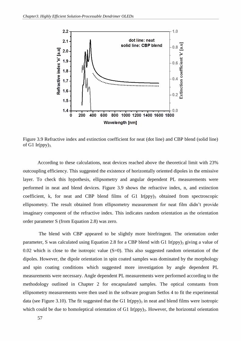
Chapter3. Highly Efficient Solution-Processable Dendrimer OLEDs
57
Figure 3.9 Refractive index and extinction coefficient for neat (dot line) and CBP blend (solid line)
of G1 Ir(ppy)3.
According to these calculations, neat devices reached above the theoretical limit with 23%
outcoupling efficiency. This suggested the existence of horizontally oriented dipoles in the emissive
layer. To check this hypothesis, ellipsometry and angular dependent PL measurements were
performed in neat and blend devices. Figure 3.9 shows the refractive index, n, and extinction
coefficient, k, for neat and CBP blend films of G1 Ir(ppy)3 obtained from spectroscopic
ellipsometry. The result obtained from ellipsometry measurement for neat film didn’t provide
imaginary component of the refractive index. This indicates random orientation as the orientation
order parameter S (from Equation 2.8) was zero.
The blend with CBP appeared to be slightly more birefringent. The orientation order
parameter, S was calculated using Equation 2.8 for a CBP blend with G1 Ir(ppy)3 giving a value of
0.02 which is close to the isotropic value (S=0). This also suggested random orientation of the
dipoles. However, the dipole orientation in spin coated samples was dominated by the morphology
and spin coating conditions which suggested more investigation by angle dependent PL
measurements were necessary. Angle dependent PL measurements were performed according to the
methodology outlined in Chapter 2 for encapsulated samples. The optical constants from
ellipsometry measurements were then used in the software program Setfos 4 to fit the experimental
data (see Figure 3.10). The fit suggested that the G1 Ir(ppy)3 in neat and blend films were isotropic
which could be due to homoleptical orientation of G1 Ir(ppy)3. However, the horizontal orientation
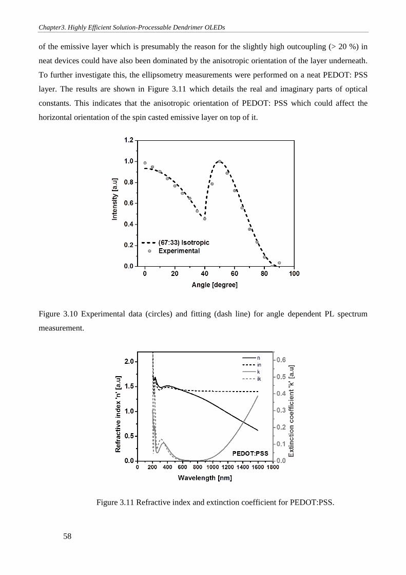
Chapter3. Highly Efficient Solution-Processable Dendrimer OLEDs
58
of the emissive layer which is presumably the reason for the slightly high outcoupling (> 20 %) in
neat devices could have also been dominated by the anisotropic orientation of the layer underneath.
To further investigate this, the ellipsometry measurements were performed on a neat PEDOT: PSS
layer. The results are shown in Figure 3.11 which details the real and imaginary parts of optical
constants. This indicates that the anisotropic orientation of PEDOT: PSS which could affect the
horizontal orientation of the spin casted emissive layer on top of it.
Figure 3.10 Experimental data (circles) and fitting (dash line) for angle dependent PL spectrum
measurement.
Figure 3.11 Refractive index and extinction coefficient for PEDOT:PSS.
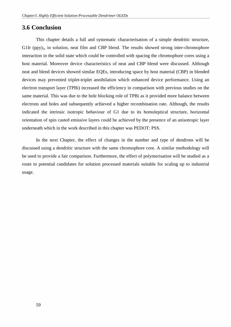
Chapter3. Highly Efficient Solution-Processable Dendrimer OLEDs
59
3.6 Conclusion
This chapter details a full and systematic characterisation of a simple dendritic structure,
G1Ir (ppy)3, in solution, neat film and CBP blend. The results showed strong inter-chromophore
interaction in the solid state which could be controlled with spacing the chromophore cores using a
host material. Moreover device characteristics of neat and CBP blend were discussed. Although
neat and blend devices showed similar EQEs, introducing space by host material (CBP) in blended
devices may prevented triplet-triplet annihilation which enhanced device performance. Using an
electron transport layer (TPBi) increased the efficiency in comparison with previous studies on the
same material. This was due to the hole blocking role of TPBi as it provided more balance between
electrons and holes and subsequently achieved a higher recombination rate. Although, the results
indicated the intrinsic isotropic behaviour of G1 due to its homoleptical structure, horizontal
orientation of spin casted emissive layers could be achieved by the presence of an anisotropic layer
underneath which in the work described in this chapter was PEDOT: PSS.
In the next Chapter, the effect of changes in the number and type of dendrons will be
discussed using a dendritic structure with the same chromophore core. A similar methodology will
be used to provide a fair comparison. Furthermore, the effect of polymerisation will be studied as a
route to potential candidates for solution processed materials suitable for scaling up to industrial
usage.
Chapter3. Highly Efficient Solution-Processable Dendrimer OLEDs
60
References
[1] C. Adachi, M.A. Baldo, M.E. Thompson, S.R. Forrest, Nearly 100% internal phosphorescence
efficiency in an organic light-emitting device, Journal of Applied Physics, 90 (2001) 5048-5051.
[2] M. Baldo, S. Lamansky, P. Burrows, M. Thompson, S. Forrest, Very high-efficiency green
organic light-emitting devices based on electrophosphorescence, Applied Physics Letters, 75 (1999)
4.
[3] J. Wilson, A. Dhoot, A. Seeley, M. Khan, A. Köhler, R. Friend, Spin-dependent exciton
formation in π-conjugated compounds, Nature, 413 (2001) 828-831.
[4] C. Adachi, R.C. Kwong, P. Djurovich, V. Adamovich, M.A. Baldo, M.E. Thompson, S.R.
Forrest, Endothermic energy transfer: A mechanism for generating very efficient high-energy
phosphorescent emission in organic materials, Applied Physics Letters, 79 (2001) 2082-2084.
[5] C. Adachi, M.A. Baldo, S.R. Forrest, S. Lamansky, M.E. Thompson, R.C. Kwong, High-
efficiency red electrophosphorescence devices, Applied Physics Letters, 78 (2001) 1622-1624.
[6] M. Baldo, M. Thompson, S. Forrest, High-efficiency fluorescent organic light-emitting devices
using a phosphorescent sensitizer, Nature, 403 (2000) 750-753.
[7] S.-C. Lo, C.P. Shipley, R.N. Bera, R.E. Harding, A.R. Cowley, P.L. Burn, I.D. Samuel, Blue
phosphorescence from iridium (III) complexes at room temperature, Chemistry of materials, 18
(2006) 5119-5129.
[8] Y. You, S.Y. Park, Phosphorescent iridium (III) complexes: toward high phosphorescence
quantum efficiency through ligand control, Dalton Transactions, (2009) 1267-1282.
[9] Y.C. Chiu, J.Y. Hung, Y. Chi, C.C. Chen, C.H. Chang, C.C. Wu, Y.M. Cheng, Y.C. Yu, G.H.
Lee, P.T. Chou, En Route to High External Quantum Efficiency (∼ 12%), Organic True‐Blue‐Light‐Emitting Diodes Employing Novel Design of Iridium (III) Phosphors, Advanced Materials,
21 (2009) 2221-2225.
[10] E. Holder, B.M. Langeveld, U.S. Schubert, New trends in the use of transition metal-ligand
complexes for applications in electroluminescent devices, Advanced Materials, 17 (2005) 1109-
1121.
[11] Q. Huang, K. Walzer, M. Pfeiffer, V. Lyssenko, G. He, K. Leo, Highly efficient top emitting
organic light-emitting diodes with organic outcoupling enhancement layers, Applied physics letters,
88 (2006) 3515.
[12] X. Chen, J.-L. Liao, Y. Liang, M. Ahmed, H.-E. Tseng, S.-A. Chen, High-efficiency red-light
emission from polyfluorenes grafted with cyclometalated iridium complexes and charge transport
moiety, Journal of the American Chemical Society, 125 (2003) 636-637.
[13] A.J. Sandee, C.K. Williams, N.R. Evans, J.E. Davies, C.E. Boothby, A. Köhler, R.H. Friend,
A.B. Holmes, Solution-processible conjugated electrophosphorescent polymers, Journal of the
American Chemical Society, 126 (2004) 7041-7048.
[14] H. Zhen, C. Luo, W. Yang, W. Song, B. Du, J. Jiang, C. Jiang, Y. Zhang, Y. Cao,
Electrophosphorescent chelating copolymers based on linkage isomers of naphthylpyridine-iridium
complexes with fluorene, Macromolecules, 39 (2006) 1693-1700.
[15] P.L. Burn, S.C. Lo, I.D. Samuel, The Development of Light‐Emitting Dendrimers for Displays,
Advanced Materials, 19 (2007) 1675-1688.
[16] S.-C. Lo, E.B. Namdas, C.P. Shipley, J.P. Markham, T.D. Anthopolous, P.L. Burn, I.D.
Samuel, The synthesis and properties of iridium cored dendrimers with carbazole dendrons, Organic
electronics, 7 (2006) 85-98.
[17] S.-C. Lo, P.L. Burn, Development of dendrimers: macromolecules for use in organic light-
emitting diodes and solar cells, Chemical reviews, 107 (2007) 1097-1116.
[18] S.-C. Lo, R.E. Harding, E. Brightman, P.L. Burn, I.D. Samuel, The development of
phenylethylene dendrons for blue phosphorescent emitters, Journal of Materials Chemistry, 19
(2009) 3213-3227.
Chapter3. Highly Efficient Solution-Processable Dendrimer OLEDs
61
[19] T. Hebner, C. Wu, D. Marcy, M. Lu, J. Sturm, Ink-jet printing of doped polymers for organic
light emitting devices, Applied Physics Letters, 72 (1998) 519-521.
[20] J. Ding, J. Gao, Y. Cheng, Z. Xie, L. Wang, D. Ma, X. Jing, F. Wang, Highly Efficient Green‐Emitting Phosphorescent Iridium Dendrimers Based on Carbazole Dendrons, Advanced Functional
Materials, 16 (2006) 575-581.
[21] S. Hecht, J.M. Fréchet, Dendritic encapsulation of function: applying nature's site isolation
principle from biomimetics to materials science, Angewandte Chemie International Edition, 40
(2001) 74-91.
[22] T. Tsuzuki, N. Shirasawa, T. Suzuki, S. Tokito, Organic light-emitting diodes using
multifunctional phosphorescent dendrimers with iridium-complex core and charge-transporting
dendrons, Japanese journal of applied physics, 44 (2005) 4151.
[23] M. Velusamy, K.J. Thomas, C.-H. Chen, J.T. Lin, Y.S. Wen, W.-T. Hsieh, C.-H. Lai, P.-T.
Chou, Synthesis, structure and electroluminescent properties of cyclometalated iridium complexes
possessing sterically hindered ligands, Dalton Transactions, (2007) 3025-3034.
[24] J. Markham, S.-C. Lo, S. Magennis, P. Burn, I. Samuel, High-efficiency green
phosphorescence from spin-coated single-layer dendrimer light-emitting diodes, Applied physics
letters, 80 (2002) 2645-2647.
[25] Y. Tao, C. Yang, J. Qin, Organic host materials for phosphorescent organic light-emitting
diodes, Chemical Society Reviews, 40 (2011) 2943-2970.
[26] H. Fukagawa, K. Watanabe, S. Tokito, Efficient white organic light emitting diodes with
solution processed and vacuum deposited emitting layers, Organic Electronics, 10 (2009) 798-802.
[27] E.B. Namdas, A. Ruseckas, I.D. Samuel, S.-C. Lo, P.L. Burn, Photophysics of fac-tris (2-
phenylpyridine) iridium (III) cored electroluminescent dendrimers in solution and films, The
Journal of Physical Chemistry B, 108 (2004) 1570-1577.
[28] A. Boudrioua, P. Hobson, B. Matterson, I. Samuel, W. Barnes, Birefringence and dispersion of
the light emitting polymer MEH–PPV, Synthetic metals, 111 (2000) 545-547.
62
Chapter 4
Effects of Polymerisation and
Dendronisation on iridium (III) OLEDs
4.1 Introduction
In organic light emitting diodes, a key property requirement of the material is a high
photoluminescence quantum yield. It is now widely recognized that OLED materials also need to
have sufficient charge mobility to avoid high driving voltages. In Chapter 3, a first generation
Iridium dendrimer (with electrically insulating biphenyl dendrons) was described as a candidate for
solution processed OLEDs. One option to improve the charge transport and potentially therefore the
efficiency of OLED devices would be to incorporate a charge-transporting moiety within the device
or dendrimer structure. Carbazole-based compounds are well-known as high mobility hole-
transporting materials and accordingly, they have been used widely in phosphorescent metal
complexes OLEDs as host materials [1, 2] and within host free dendrimers in which the carbazole
unit makes up the dendron [3, 4]. The inclusion of the carbazole dendrons within Iridium III (Ir)
complexes by covalent bonding, results in the formation of a single multifunctional dendrimer in
which the carbazole serves indirectly as the host material while the Ir (III) core acts as an emissive
dopant. The main benefit of this approach over doped devices is that phase separation is avoided,
leading to higher device performance [5].
It has been found that first generation dendrons are insufficient to prevent interactions
between the emissive core[6]. Although higher generation dendrons will sufficiently reduce the
internal interactions to maintain a high PLQY, they usually cause a significant reduction in charge
transport[7, 8]. A compromise therefore exists that the intermolecular interactions that affect the
quenching in luminescent materials can be controlled by the number of dendrons [4, 9-11].
Dendrons can be used as branched shells surrounding the Ir complex to prevent self-aggregation
and concentration quenching of the emissive core in the solid state. Singly-dendronised dendrimers
have an opened face of the core chromophore which lends them susceptible to intermolecular
interaction. This issue can be resolved by creating so-called “doubly-dendronised dendrimers”
which have two dendrons attached to each ligand of the core[12, 13].
Chapter 4. Effects of Polymerisation and Dendronisation on iridium (III) OLEDs
63
Phosphorescent dendrimer materials with suitable dendrons can be used to make highly
efficient solution processed OLEDs[4]. Nevertheless, the viscosity of these dendrimer solutions
under standard processing concentrations is only slightly greater than the solvent they are dissolved
in, and this viscosity is too low for solution processed mass production methods such as inkjet
printing [14-16]. This is the motivation for exploring a new approach to the phosphorescent
materials in the form of iridium (III) poly(dendrimers). It is anticipated that these materials would
simultaneously improve the solution processibility whilst giving the material the better film forming
needed for roll to roll or inkjet printing [13, 17, 18].
This Chapter first describes the pre-fabrication characterisation of a hostless dendrimer with
a single carbazole Dendron, followed by its performance in a device. Next, the study focused on
how polymerisation of this compound in order to achieve the desire film quality for printing
techniques enhances the device performance and photophysical properties. Finally, the effect of
introducing an additional carbazole dendron to the system will be described via a similar
methodology on both doubly-dendronised dendrimer and the poly(dendrimer) analogues.
4.2 Singly-dendronised dendrimer and poly(dendrimer)
4.2.1 Material design and experimental methods
The chemical structure of singly-dendronised dendrimer (D1) and poly(dendrimer) (P1) are
shown in Figure 4.1.a and b; both molecules consist of an Ir (III) core encapsulated within a set of
carbazole dendrons. The poly(dendrimers) P1 was synthesized using Ring Opening Metathesis
Polymerisation (ROMP) as it has been found to be an effective route for joining together bulky
dendrimeric monomers with high Mws[19, 20]. It has been shown that the use of conjugated
polymers such as poly(fluorene) for phosphorescent emitters is problematic since they have low
triplet energy. This leads to a reduction in the PLQY due to back transfer of triplet excitation from
the phosphorescent emitter to the polymer [21, 22]. Therefore a norbornenyl-based non-conjugated
polymer backbone was used with dendrimer side-chains to make the poly(dendrimers).
In addition, two small molecules commercially available from Lumtec, 4,4’-N,N’-
dicarbazolyl-biphenyl (CBP) and 2,2',2"-(1,3,5-Benzinetriyl)-tris(1-phenyl-1-H-benzimidazole)
(TPBi) were used as host and electron transport materials, respectively, shown in a previous
Chapter (Figure 3.1.b and c).
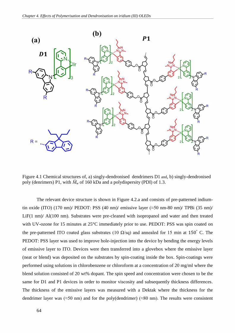
Chapter 4. Effects of Polymerisation and Dendronisation on iridium (III) OLEDs
64
Figure 4.1 Chemical structures of, a) singly-dendronised dendrimers D1 and, b) singly-dendronised
poly (denrimers) P1, with M̅w of 160 kDa and a polydispersity (PDI) of 1.3.
The relevant device structure is shown in Figure 4.2.a and consists of pre-patterned indium-
tin oxide (ITO) (170 nm)/ PEDOT: PSS (40 nm)/ emissive layer (≈50 nm-80 nm)/ TPBi (35 nm)/
LiF(1 nm)/ Al(100 nm). Substrates were pre-cleaned with isopropanol and water and then treated
with UV-ozone for 15 minutes at 25°C immediately prior to use. PEDOT: PSS was spin coated on
the pre-patterned ITO coated glass substrates (10 Ω/sq) and annealed for 15 min at 150° C. The
PEDOT: PSS layer was used to improve hole-injection into the device by bending the energy levels
of emissive layer to ITO. Devices were then transferred into a glovebox where the emissive layer
(neat or blend) was deposited on the substrates by spin-coating inside the box. Spin-coatings were
performed using solutions in chlorobenzene or chloroform at a concentration of 20 mg/ml where the
blend solution consisted of 20 wt% dopant. The spin speed and concentration were chosen to be the
same for D1 and P1 devices in order to monitor viscosity and subsequently thickness differences.
The thickness of the emissive layers was measured with a Dektak where the thickness for the
dendrimer layer was (≈50 nm) and for the poly(dendrimer) (≈80 nm). The results were consistent
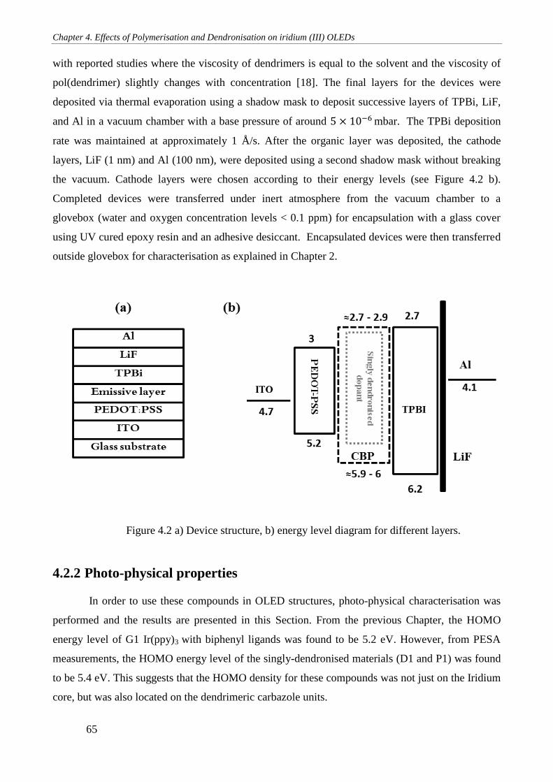
Chapter 4. Effects of Polymerisation and Dendronisation on iridium (III) OLEDs
65
with reported studies where the viscosity of dendrimers is equal to the solvent and the viscosity of
pol(dendrimer) slightly changes with concentration [18]. The final layers for the devices were
deposited via thermal evaporation using a shadow mask to deposit successive layers of TPBi, LiF,
and Al in a vacuum chamber with a base pressure of around 5 × 10⁻⁶ mbar. The TPBi deposition
rate was maintained at approximately 1 Å/s. After the organic layer was deposited, the cathode
layers, LiF (1 nm) and Al (100 nm), were deposited using a second shadow mask without breaking
the vacuum. Cathode layers were chosen according to their energy levels (see Figure 4.2 b).
Completed devices were transferred under inert atmosphere from the vacuum chamber to a
glovebox (water and oxygen concentration levels < 0.1 ppm) for encapsulation with a glass cover
using UV cured epoxy resin and an adhesive desiccant. Encapsulated devices were then transferred
outside glovebox for characterisation as explained in Chapter 2.
Figure 4.2 a) Device structure, b) energy level diagram for different layers.
4.2.2 Photo-physical properties
In order to use these compounds in OLED structures, photo-physical characterisation was
performed and the results are presented in this Section. From the previous Chapter, the HOMO
energy level of G1 Ir(ppy)3 with biphenyl ligands was found to be 5.2 eV. However, from PESA
measurements, the HOMO energy level of the singly-dendronised materials (D1 and P1) was found
to be 5.4 eV. This suggests that the HOMO density for these compounds was not just on the Iridium
core, but was also located on the dendrimeric carbazole units.
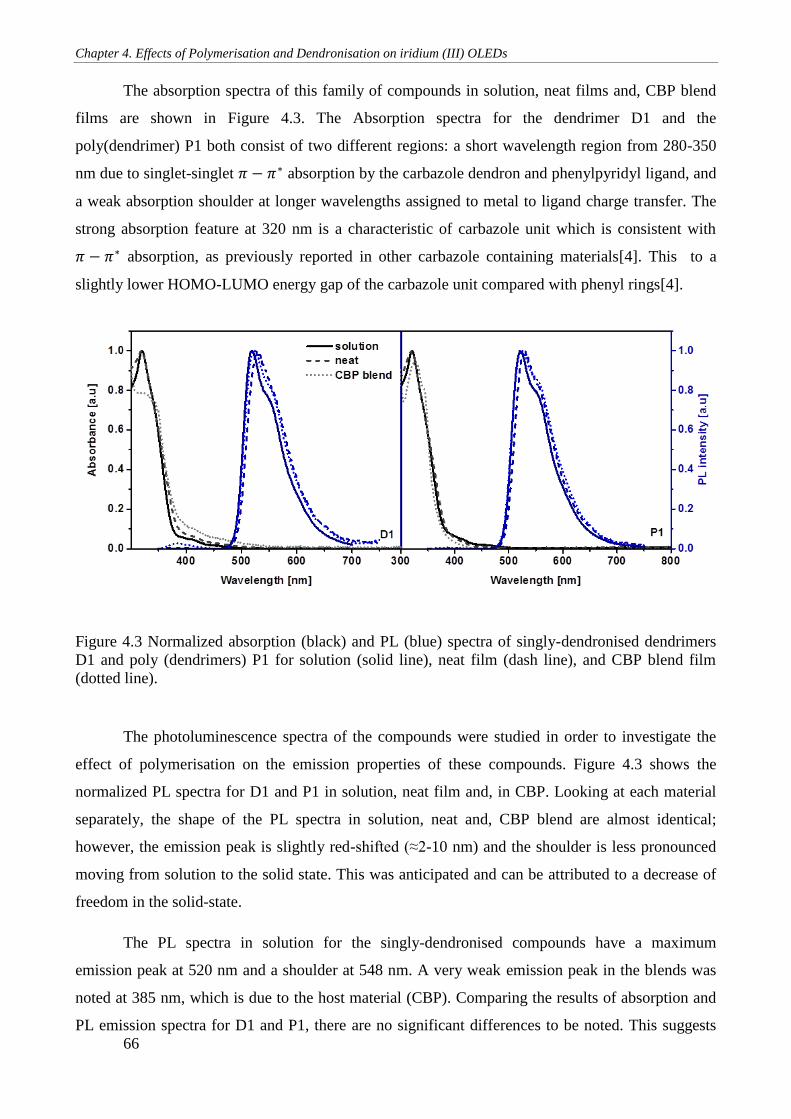
Chapter 4. Effects of Polymerisation and Dendronisation on iridium (III) OLEDs
66
The absorption spectra of this family of compounds in solution, neat films and, CBP blend
films are shown in Figure 4.3. The Absorption spectra for the dendrimer D1 and the
poly(dendrimer) P1 both consist of two different regions: a short wavelength region from 280-350
nm due to singlet-singlet 𝜋 − 𝜋∗ absorption by the carbazole dendron and phenylpyridyl ligand, and
a weak absorption shoulder at longer wavelengths assigned to metal to ligand charge transfer. The
strong absorption feature at 320 nm is a characteristic of carbazole unit which is consistent with
𝜋 − 𝜋∗ absorption, as previously reported in other carbazole containing materials[4]. This to a
slightly lower HOMO-LUMO energy gap of the carbazole unit compared with phenyl rings[4].
Figure 4.3 Normalized absorption (black) and PL (blue) spectra of singly-dendronised dendrimers
D1 and poly (dendrimers) P1 for solution (solid line), neat film (dash line), and CBP blend film
(dotted line).
The photoluminescence spectra of the compounds were studied in order to investigate the
effect of polymerisation on the emission properties of these compounds. Figure 4.3 shows the
normalized PL spectra for D1 and P1 in solution, neat film and, in CBP. Looking at each material
separately, the shape of the PL spectra in solution, neat and, CBP blend are almost identical;
however, the emission peak is slightly red-shifted (≈2-10 nm) and the shoulder is less pronounced
moving from solution to the solid state. This was anticipated and can be attributed to a decrease of
freedom in the solid-state.
The PL spectra in solution for the singly-dendronised compounds have a maximum
emission peak at 520 nm and a shoulder at 548 nm. A very weak emission peak in the blends was
noted at 385 nm, which is due to the host material (CBP). Comparing the results of absorption and
PL emission spectra for D1 and P1, there are no significant differences to be noted. This suggests
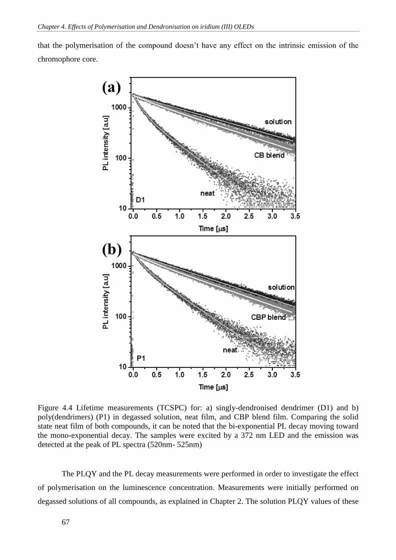
Chapter 4. Effects of Polymerisation and Dendronisation on iridium (III) OLEDs
67
that the polymerisation of the compound doesn’t have any effect on the intrinsic emission of the
chromophore core.
Figure 4.4 Lifetime measurements (TCSPC) for: a) singly-dendronised dendrimer (D1) and b)
poly(dendrimers) (P1) in degassed solution, neat film, and CBP blend film. Comparing the solid
state neat film of both compounds, it can be noted that the bi-exponential PL decay moving toward
the mono-exponential decay. The samples were excited by a 372 nm LED and the emission was
detected at the peak of PL spectra (520nm- 525nm)
The PLQY and the PL decay measurements were performed in order to investigate the effect
of polymerisation on the luminescence concentration. Measurements were initially performed on
degassed solutions of all compounds, as explained in Chapter 2. The solution PLQY values of these
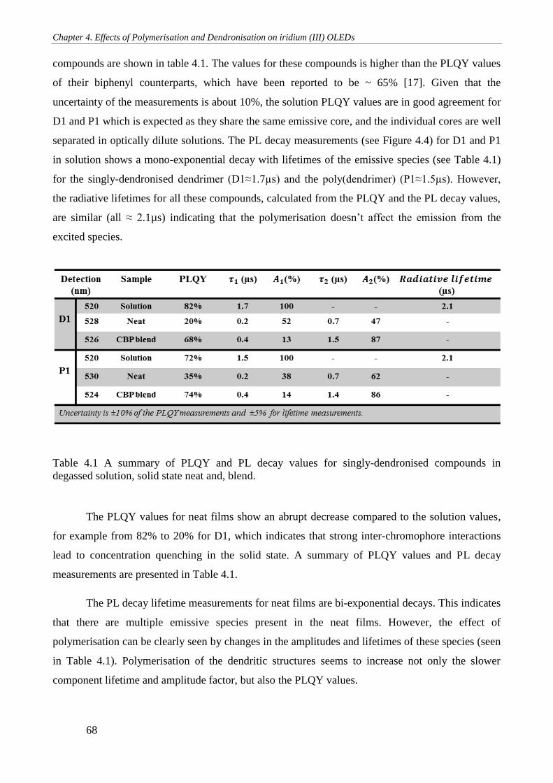
Chapter 4. Effects of Polymerisation and Dendronisation on iridium (III) OLEDs
68
compounds are shown in table 4.1. The values for these compounds is higher than the PLQY values
of their biphenyl counterparts, which have been reported to be ~ 65% [17]. Given that the
uncertainty of the measurements is about 10%, the solution PLQY values are in good agreement for
D1 and P1 which is expected as they share the same emissive core, and the individual cores are well
separated in optically dilute solutions. The PL decay measurements (see Figure 4.4) for D1 and P1
in solution shows a mono-exponential decay with lifetimes of the emissive species (see Table 4.1)
for the singly-dendronised dendrimer (D1≈1.7µs) and the poly(dendrimer) (P1≈1.5µs). However,
the radiative lifetimes for all these compounds, calculated from the PLQY and the PL decay values,
are similar (all ≈ 2.1µs) indicating that the polymerisation doesn’t affect the emission from the
excited species.
Table 4.1 A summary of PLQY and PL decay values for singly-dendronised compounds in
degassed solution, solid state neat and, blend.
The PLQY values for neat films show an abrupt decrease compared to the solution values,
for example from 82% to 20% for D1, which indicates that strong inter-chromophore interactions
lead to concentration quenching in the solid state. A summary of PLQY values and PL decay
measurements are presented in Table 4.1.
The PL decay lifetime measurements for neat films are bi-exponential decays. This indicates
that there are multiple emissive species present in the neat films. However, the effect of
polymerisation can be clearly seen by changes in the amplitudes and lifetimes of these species (seen
in Table 4.1). Polymerisation of the dendritic structures seems to increase not only the slower
component lifetime and amplitude factor, but also the PLQY values.
Chapter 4. Effects of Polymerisation and Dendronisation on iridium (III) OLEDs
69
In order to further decrease the concentration quenching between cores, these compounds
were blended with CBP. The photo-physical properties for these compounds were investigated in
20% wt CBP blends and are shown in Table 4.1. The solid state PLQY of these blends increases,
showing a similar trend to that observed with the solution PLQY measurements. Moreover, the
lifetime decays show a bigger ratio of the slower components with a more similar lifetime to the
solution. Both of these values are consistent with each other, showing that there are still inter-
chromophore interactions that are not completely controlled in CBP blends. The lifetime of the CBP
emissive peak at 385 nm which was observed in the blends (see Figure 4.3) - was reported to be on
the order of ns [23], which was faster than the time resolution of our instrument.
4.2.3 Device performance
To assess whether the high photoluminescence efficiency found in the solid state for these
compounds could lead to efficient OLEDs, a number of devices were fabricated. This Section
presents the results of these devices.
The typical electrical characteristics of D1 and P1 is shown in Figure 4.5 for neat and CBP
blend devices. TPBi was used in all the devices as it was shown in Chapter 3 that TPBI not only
facilitates the electron injection, but increases the recombination rate by blocking holes, which both
of these processes lead to higher EQE values. Neat devices were tested to lower voltages to avoid
triplet-triplet annihilation and demonstrated quick roll off, as shown in neat devices of D1 (see
Figure 4. 5. a). Although similar values of luminance and current density were obtained for both
compounds, there are distinct differences in the performances of neat and blend-based devices. In
neat devices, slightly higher turn on voltages were observed for poly(dendrimer) devices (4.6V) in
comparison with the dendrimer (3.5 V), which is consistent with the slightly thicker active layer.
The neat devices showed sharper current and luminance increases with lower turn on
voltage in comparison with their CBP blend counterparts for each material. It is clear that they pass
higher current density through devices at the same voltage in comparison with the blended devices.
There are multiple possible reasons for this including, for example, better interfaces in the neat
devices or better charge injection into the neat devices. Polymerisation seems to slightly improve
the performance and this could be due to providing higher viscosity, better film forming or better
packing and morphology.
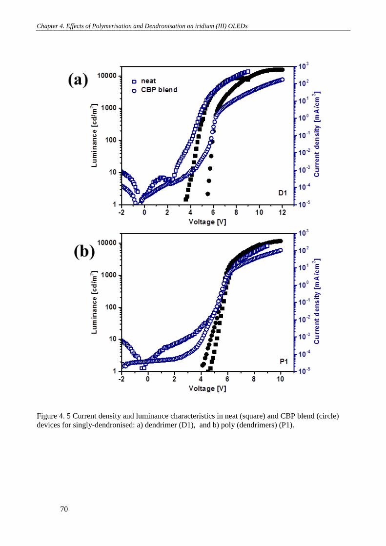
Chapter 4. Effects of Polymerisation and Dendronisation on iridium (III) OLEDs
70
Figure 4. 5 Current density and luminance characteristics in neat (square) and CBP blend (circle)
devices for singly-dendronised: a) dendrimer (D1), and b) poly (dendrimers) (P1).
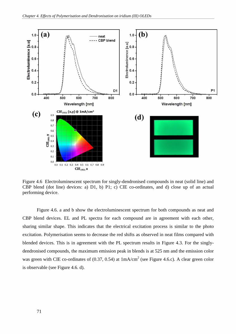
Chapter 4. Effects of Polymerisation and Dendronisation on iridium (III) OLEDs
71
Figure 4.6 Electroluminescent spectrum for singly-dendronised compounds in neat (solid line) and
CBP blend (dot line) devices: a) D1, b) P1; c) CIE co-ordinates, and d) close up of an actual
performing device.
Figure 4.6. a and b show the electroluminescent spectrum for both compounds as neat and
CBP blend devices. EL and PL spectra for each compound are in agreement with each other,
sharing similar shape. This indicates that the electrical excitation process is similar to the photo
excitation. Polymerisation seems to decrease the red shifts as observed in neat films compared with
blended devices. This is in agreement with the PL spectrum results in Figure 4.3. For the singly-
dendronised compounds, the maximum emission peak in blends is at 525 nm and the emission color
was green with CIE co-ordinates of (0.37, 0.54) at 1mA/cm2 (see Figure 4.6.c). A clear green color
is observable (see Figure 4.6. d).
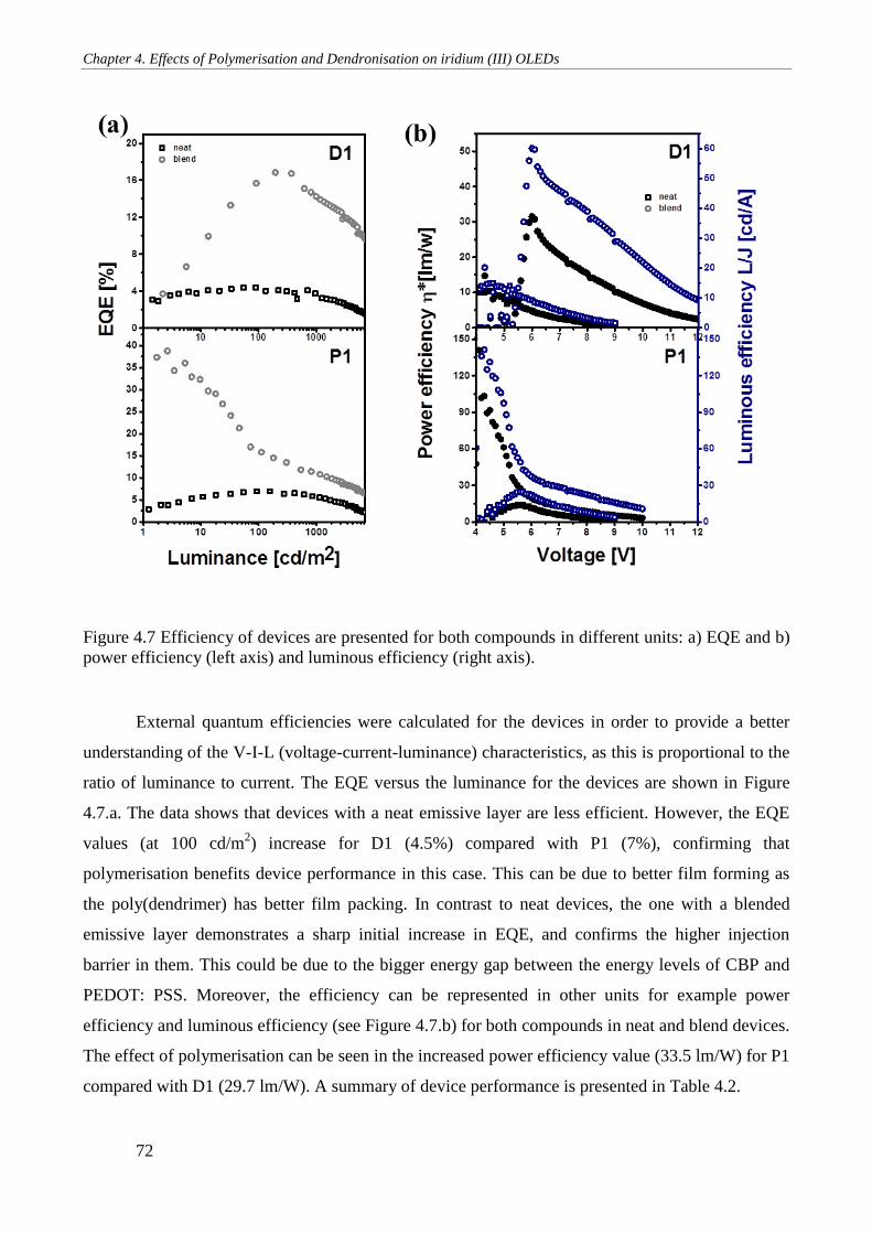
Chapter 4. Effects of Polymerisation and Dendronisation on iridium (III) OLEDs
72
Figure 4.7 Efficiency of devices are presented for both compounds in different units: a) EQE and b)
power efficiency (left axis) and luminous efficiency (right axis).
External quantum efficiencies were calculated for the devices in order to provide a better
understanding of the V-I-L (voltage-current-luminance) characteristics, as this is proportional to the
ratio of luminance to current. The EQE versus the luminance for the devices are shown in Figure
4.7.a. The data shows that devices with a neat emissive layer are less efficient. However, the EQE
values (at 100 cd/m2) increase for D1 (4.5%) compared with P1 (7%), confirming that
polymerisation benefits device performance in this case. This can be due to better film forming as
the poly(dendrimer) has better film packing. In contrast to neat devices, the one with a blended
emissive layer demonstrates a sharp initial increase in EQE, and confirms the higher injection
barrier in them. This could be due to the bigger energy gap between the energy levels of CBP and
PEDOT: PSS. Moreover, the efficiency can be represented in other units for example power
efficiency and luminous efficiency (see Figure 4.7.b) for both compounds in neat and blend devices.
The effect of polymerisation can be seen in the increased power efficiency value (33.5 lm/W) for P1
compared with D1 (29.7 lm/W). A summary of device performance is presented in Table 4.2.
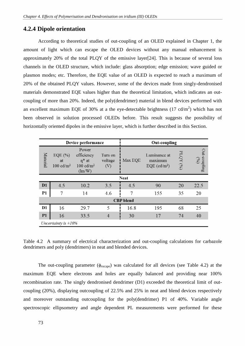
Chapter 4. Effects of Polymerisation and Dendronisation on iridium (III) OLEDs
73
4.2.4 Dipole orientation
According to theoretical studies of out-coupling of an OLED explained in Chapter 1, the
amount of light which can escape the OLED devices without any manual enhancement is
approximately 20% of the total PLQY of the emissive layer[24]. This is because of several loss
channels in the OLED structure, which include: glass absorption; edge emission; wave guided or
plasmon modes; etc. Therefore, the EQE value of an OLED is expected to reach a maximum of
20% of the obtained PLQY values. However, some of the devices made from singly-dendronised
materials demonstrated EQE values higher than the theoretical limitation, which indicates an out-
coupling of more than 20%. Indeed, the poly(dendrimer) material in blend devices performed with
an excellent maximum EQE of 30% at a the eye-detectable brightness (17 cd/m2) which has not
been observed in solution processed OLEDs before. This result suggests the possibility of
horizontally oriented dipoles in the emissive layer, which is further described in this Section.
Table 4.2 A summary of electrical characterization and out-coupling calculations for carbazole
dendrimers and poly (dendrimers) in neat and blended devices.
The out-coupling parameter (ϕescape) was calculated for all devices (see Table 4.2) at the
maximum EQE where electrons and holes are equally balanced and providing near 100%
recombination rate. The singly dendronised dendrimer (D1) exceeded the theoretical limit of out-
coupling (20%), displaying outcoupling of 22.5% and 25% in neat and blend devices respectively
and moreover outstanding outcoupling for the poly(dendrimer) P1 of 40%. Variable angle
spectroscopic ellipsometry and angle dependent PL measurements were performed for these
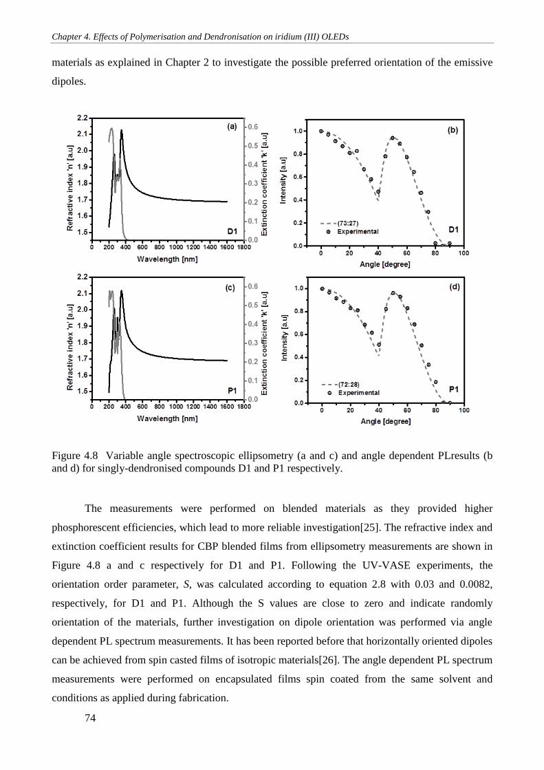
Chapter 4. Effects of Polymerisation and Dendronisation on iridium (III) OLEDs
74
materials as explained in Chapter 2 to investigate the possible preferred orientation of the emissive
dipoles.
Figure 4.8 Variable angle spectroscopic ellipsometry (a and c) and angle dependent PLresults (b
and d) for singly-dendronised compounds D1 and P1 respectively.
The measurements were performed on blended materials as they provided higher
phosphorescent efficiencies, which lead to more reliable investigation[25]. The refractive index and
extinction coefficient results for CBP blended films from ellipsometry measurements are shown in
Figure 4.8 a and c respectively for D1 and P1. Following the UV-VASE experiments, the
orientation order parameter, S, was calculated according to equation 2.8 with 0.03 and 0.0082,
respectively, for D1 and P1. Although the S values are close to zero and indicate randomly
orientation of the materials, further investigation on dipole orientation was performed via angle
dependent PL spectrum measurements. It has been reported before that horizontally oriented dipoles
can be achieved from spin casted films of isotropic materials[26]. The angle dependent PL spectrum
measurements were performed on encapsulated films spin coated from the same solvent and
conditions as applied during fabrication.
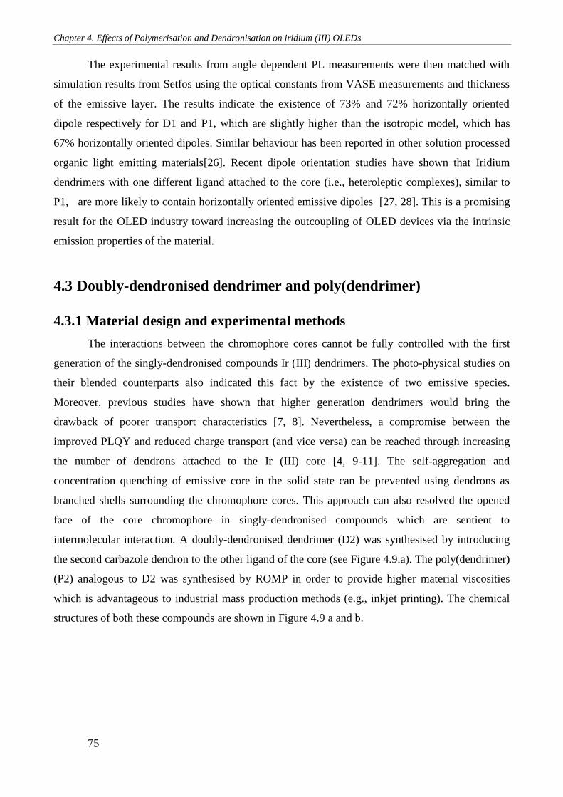
Chapter 4. Effects of Polymerisation and Dendronisation on iridium (III) OLEDs
75
The experimental results from angle dependent PL measurements were then matched with
simulation results from Setfos using the optical constants from VASE measurements and thickness
of the emissive layer. The results indicate the existence of 73% and 72% horizontally oriented
dipole respectively for D1 and P1, which are slightly higher than the isotropic model, which has
67% horizontally oriented dipoles. Similar behaviour has been reported in other solution processed
organic light emitting materials[26]. Recent dipole orientation studies have shown that Iridium
dendrimers with one different ligand attached to the core (i.e., heteroleptic complexes), similar to
P1, are more likely to contain horizontally oriented emissive dipoles [27, 28]. This is a promising
result for the OLED industry toward increasing the outcoupling of OLED devices via the intrinsic
emission properties of the material.
4.3 Doubly-dendronised dendrimer and poly(dendrimer)
4.3.1 Material design and experimental methods
The interactions between the chromophore cores cannot be fully controlled with the first
generation of the singly-dendronised compounds Ir (III) dendrimers. The photo-physical studies on
their blended counterparts also indicated this fact by the existence of two emissive species.
Moreover, previous studies have shown that higher generation dendrimers would bring the
drawback of poorer transport characteristics [7, 8]. Nevertheless, a compromise between the
improved PLQY and reduced charge transport (and vice versa) can be reached through increasing
the number of dendrons attached to the Ir (III) core [4, 9-11]. The self-aggregation and
concentration quenching of emissive core in the solid state can be prevented using dendrons as
branched shells surrounding the chromophore cores. This approach can also resolved the opened
face of the core chromophore in singly-dendronised compounds which are sentient to
intermolecular interaction. A doubly-dendronised dendrimer (D2) was synthesised by introducing
the second carbazole dendron to the other ligand of the core (see Figure 4.9.a). The poly(dendrimer)
(P2) analogous to D2 was synthesised by ROMP in order to provide higher material viscosities
which is advantageous to industrial mass production methods (e.g., inkjet printing). The chemical
structures of both these compounds are shown in Figure 4.9 a and b.
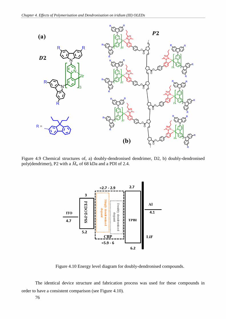
Chapter 4. Effects of Polymerisation and Dendronisation on iridium (III) OLEDs
76
Figure 4.9 Chemical structures of, a) doubly-dendronised dendrimer, D2, b) doubly-dendronised
poly(dendrimer), P2 with a M̅w of 68 kDa and a PDI of 2.4.
Figure 4.10 Energy level diagram for doubly-dendronised compounds.
The identical device structure and fabrication process was used for these compounds in
order to have a consistent comparison (see Figure 4.10).
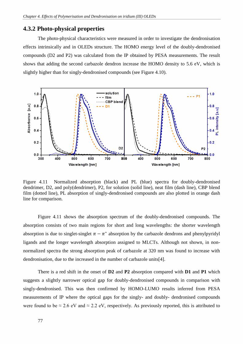
Chapter 4. Effects of Polymerisation and Dendronisation on iridium (III) OLEDs
77
4.3.2 Photo-physical properties
The photo-physical characteristics were measured in order to investigate the dendronisation
effects intrinsically and in OLEDs structure. The HOMO energy level of the doubly-dendronised
compounds (D2 and P2) was calculated from the IP obtained by PESA measurements. The result
shows that adding the second carbazole dendron increase the HOMO density to 5.6 eV, which is
slightly higher than for singly-dendronised compounds (see Figure 4.10).
Figure 4.11 Normalized absorption (black) and PL (blue) spectra for doubly-dendronised
dendrimer, D2, and poly(dendrimer), P2, for solution (solid line), neat film (dash line), CBP blend
film (dotted line), PL absorption of singly-dendronised compounds are also plotted in orange dash
line for comparison.
Figure 4.11 shows the absorption spectrum of the doubly-dendronised compounds. The
absorption consists of two main regions for short and long wavelengths: the shorter wavelength
absorption is due to singlet-singlet 𝜋 − 𝜋∗ absorption by the carbazole dendrons and phenylpyridyl
ligands and the longer wavelength absorption assigned to MLCTs. Although not shown, in non-
normalized spectra the strong absorption peak of carbazole at 320 nm was found to increase with
dendronisation, due to the increased in the number of carbazole units[4].
There is a red shift in the onset of D2 and P2 absorption compared with D1 and P1 which
suggests a slightly narrower optical gap for doubly-dendronised compounds in comparison with
singly-dendronised. This was then confirmed by HOMO-LUMO results inferred from PESA
measurements of IP where the optical gaps for the singly- and doubly- dendronised compounds
were found to be ≈ 2.6 eV and ≈ 2.2 eV, respectively. As previously reported, this is attributed to
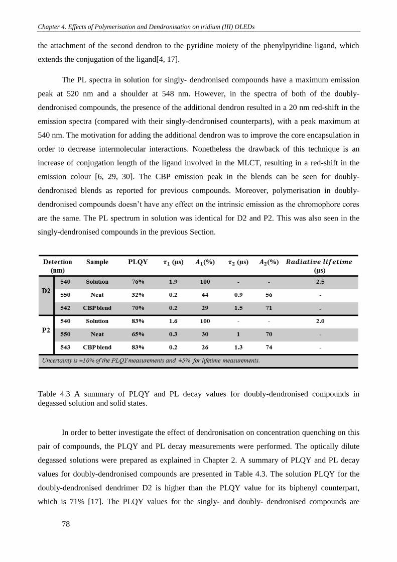
Chapter 4. Effects of Polymerisation and Dendronisation on iridium (III) OLEDs
78
the attachment of the second dendron to the pyridine moiety of the phenylpyridine ligand, which
extends the conjugation of the ligand[4, 17].
The PL spectra in solution for singly- dendronised compounds have a maximum emission
peak at 520 nm and a shoulder at 548 nm. However, in the spectra of both of the doubly-
dendronised compounds, the presence of the additional dendron resulted in a 20 nm red-shift in the
emission spectra (compared with their singly-dendronised counterparts), with a peak maximum at
540 nm. The motivation for adding the additional dendron was to improve the core encapsulation in
order to decrease intermolecular interactions. Nonetheless the drawback of this technique is an
increase of conjugation length of the ligand involved in the MLCT, resulting in a red-shift in the
emission colour [6, 29, 30]. The CBP emission peak in the blends can be seen for doubly-
dendronised blends as reported for previous compounds. Moreover, polymerisation in doubly-
dendronised compounds doesn’t have any effect on the intrinsic emission as the chromophore cores
are the same. The PL spectrum in solution was identical for D2 and P2. This was also seen in the
singly-dendronised compounds in the previous Section.
Table 4.3 A summary of PLQY and PL decay values for doubly-dendronised compounds in
degassed solution and solid states.
In order to better investigate the effect of dendronisation on concentration quenching on this
pair of compounds, the PLQY and PL decay measurements were performed. The optically dilute
degassed solutions were prepared as explained in Chapter 2. A summary of PLQY and PL decay
values for doubly-dendronised compounds are presented in Table 4.3. The solution PLQY for the
doubly-dendronised dendrimer D2 is higher than the PLQY value for its biphenyl counterpart,
which is 71% [17]. The PLQY values for the singly- and doubly- dendronised compounds are
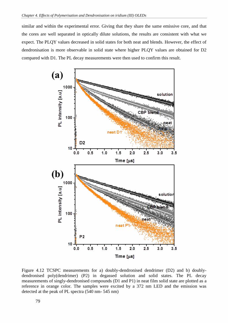
Chapter 4. Effects of Polymerisation and Dendronisation on iridium (III) OLEDs
79
similar and within the experimental error. Giving that they share the same emissive core, and that
the cores are well separated in optically dilute solutions, the results are consistent with what we
expect. The PLQY values decreased in solid states for both neat and blends. However, the effect of
dendronisation is more observable in solid state where higher PLQY values are obtained for D2
compared with D1. The PL decay measurements were then used to confirm this result.
Figure 4.12 TCSPC measurements for a) doubly-dendronised dendrimer (D2) and b) doubly-
dendronised poly(dendrimer) (P2) in degassed solution and solid states. The PL decay
measurements of singly-dendronised compounds (D1 and P1) in neat film solid state are plotted as a
reference in orange color. The samples were excited by a 372 nm LED and the emission was
detected at the peak of PL spectra (540 nm- 545 nm)
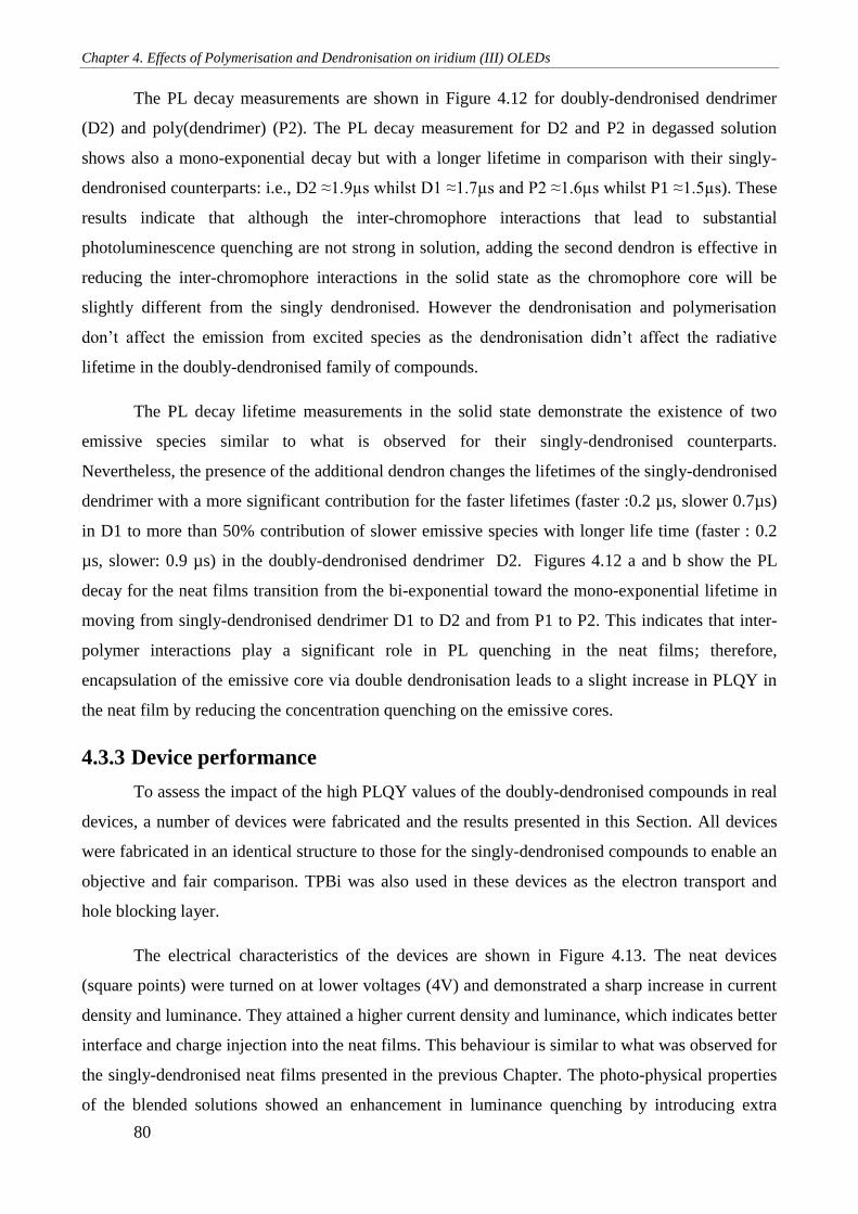
Chapter 4. Effects of Polymerisation and Dendronisation on iridium (III) OLEDs
80
The PL decay measurements are shown in Figure 4.12 for doubly-dendronised dendrimer
(D2) and poly(dendrimer) (P2). The PL decay measurement for D2 and P2 in degassed solution
shows also a mono-exponential decay but with a longer lifetime in comparison with their singly-
dendronised counterparts: i.e., D2 ≈1.9µs whilst D1 ≈1.7µs and P2 ≈1.6µs whilst P1 ≈1.5µs). These
results indicate that although the inter-chromophore interactions that lead to substantial
photoluminescence quenching are not strong in solution, adding the second dendron is effective in
reducing the inter-chromophore interactions in the solid state as the chromophore core will be
slightly different from the singly dendronised. However the dendronisation and polymerisation
don’t affect the emission from excited species as the dendronisation didn’t affect the radiative
lifetime in the doubly-dendronised family of compounds.
The PL decay lifetime measurements in the solid state demonstrate the existence of two
emissive species similar to what is observed for their singly-dendronised counterparts.
Nevertheless, the presence of the additional dendron changes the lifetimes of the singly-dendronised
dendrimer with a more significant contribution for the faster lifetimes (faster :0.2 µs, slower 0.7µs)
in D1 to more than 50% contribution of slower emissive species with longer life time (faster : 0.2
µs, slower: 0.9 µs) in the doubly-dendronised dendrimer D2. Figures 4.12 a and b show the PL
decay for the neat films transition from the bi-exponential toward the mono-exponential lifetime in
moving from singly-dendronised dendrimer D1 to D2 and from P1 to P2. This indicates that inter-
polymer interactions play a significant role in PL quenching in the neat films; therefore,
encapsulation of the emissive core via double dendronisation leads to a slight increase in PLQY in
the neat film by reducing the concentration quenching on the emissive cores.
4.3.3 Device performance
To assess the impact of the high PLQY values of the doubly-dendronised compounds in real
devices, a number of devices were fabricated and the results presented in this Section. All devices
were fabricated in an identical structure to those for the singly-dendronised compounds to enable an
objective and fair comparison. TPBi was also used in these devices as the electron transport and
hole blocking layer.
The electrical characteristics of the devices are shown in Figure 4.13. The neat devices
(square points) were turned on at lower voltages (4V) and demonstrated a sharp increase in current
density and luminance. They attained a higher current density and luminance, which indicates better
interface and charge injection into the neat films. This behaviour is similar to what was observed for
the singly-dendronised neat films presented in the previous Chapter. The photo-physical properties
of the blended solutions showed an enhancement in luminance quenching by introducing extra
Chapter 4. Effects of Polymerisation and Dendronisation on iridium (III) OLEDs
81
space between the chromophore cores. Therefore a number of devices were fabricated from CBP
blend solutions to evaluate their efficiency in OLEDs. The poly(dendrimer) blend also
demonstrated a lower turn on voltage (4.9V) in comparison with the dendrimer (6V), which
indicates better injection - this can be attributed to better film formation at the interface of the
emissive layer.
Figure 4.13 Electrical characteristics in neat (square) and CBP blend (circle) devices for doubly-
dendronised :a) dendrimer D2, and b)poly(dendrimer) P2.
The EL spectra for performing devices are shown in Figure 4.14 a and b. The shape of EL
spectra are in agreement with PL spectra of the same compounds, and also with those of the singly-
dendronised compounds (D1 and P1). This indicates that dendronisation doesn’t make any change
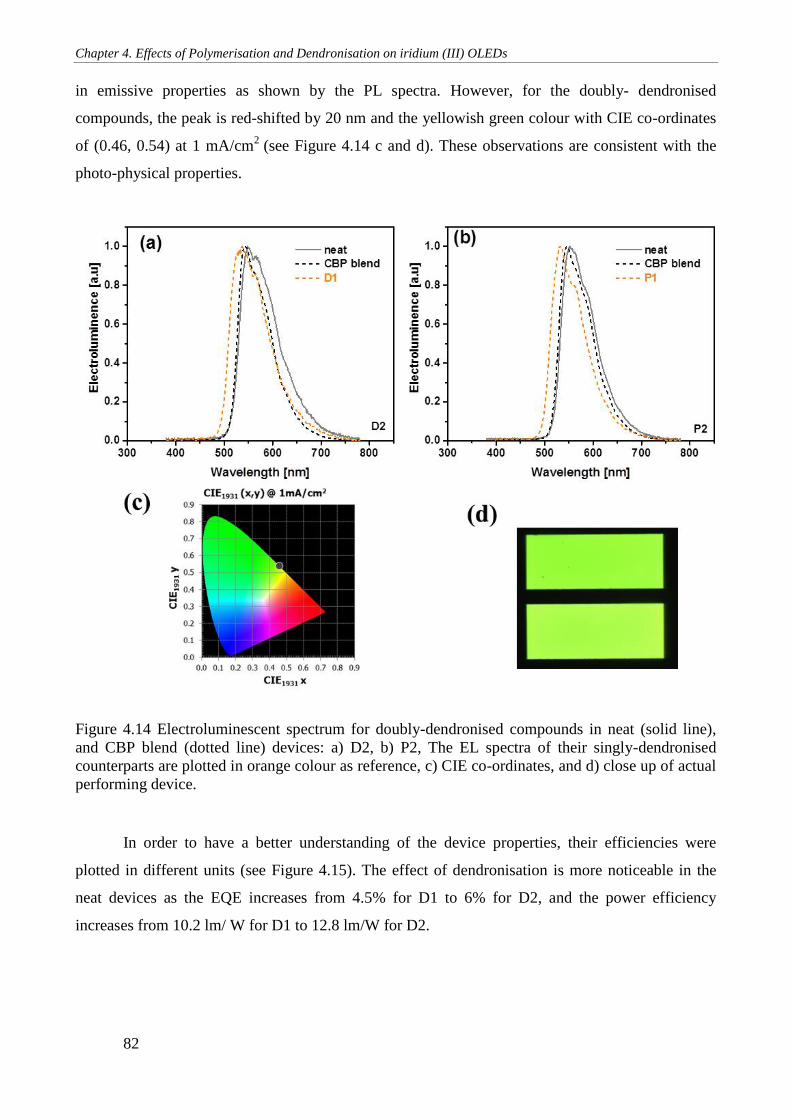
Chapter 4. Effects of Polymerisation and Dendronisation on iridium (III) OLEDs
82
in emissive properties as shown by the PL spectra. However, for the doubly- dendronised
compounds, the peak is red-shifted by 20 nm and the yellowish green colour with CIE co-ordinates
of (0.46, 0.54) at 1 mA/cm2
(see Figure 4.14 c and d). These observations are consistent with the
photo-physical properties.
Figure 4.14 Electroluminescent spectrum for doubly-dendronised compounds in neat (solid line),
and CBP blend (dotted line) devices: a) D2, b) P2, The EL spectra of their singly-dendronised
counterparts are plotted in orange colour as reference, c) CIE co-ordinates, and d) close up of actual
performing device.
In order to have a better understanding of the device properties, their efficiencies were
plotted in different units (see Figure 4.15). The effect of dendronisation is more noticeable in the
neat devices as the EQE increases from 4.5% for D1 to 6% for D2, and the power efficiency
increases from 10.2 lm/ W for D1 to 12.8 lm/W for D2.
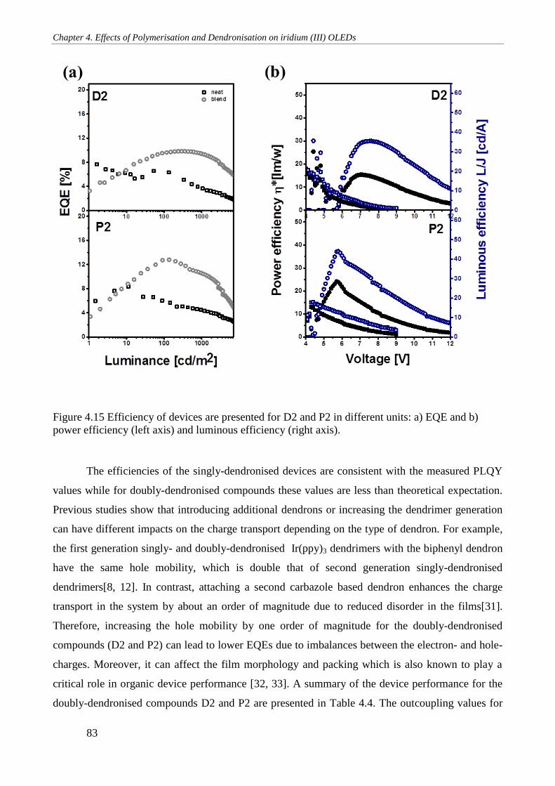
Chapter 4. Effects of Polymerisation and Dendronisation on iridium (III) OLEDs
83
Figure 4.15 Efficiency of devices are presented for D2 and P2 in different units: a) EQE and b)
power efficiency (left axis) and luminous efficiency (right axis).
The efficiencies of the singly-dendronised devices are consistent with the measured PLQY
values while for doubly-dendronised compounds these values are less than theoretical expectation.
Previous studies show that introducing additional dendrons or increasing the dendrimer generation
can have different impacts on the charge transport depending on the type of dendron. For example,
the first generation singly- and doubly-dendronised Ir(ppy)3 dendrimers with the biphenyl dendron
have the same hole mobility, which is double that of second generation singly-dendronised
dendrimers[8, 12]. In contrast, attaching a second carbazole based dendron enhances the charge
transport in the system by about an order of magnitude due to reduced disorder in the films[31].
Therefore, increasing the hole mobility by one order of magnitude for the doubly-dendronised
compounds (D2 and P2) can lead to lower EQEs due to imbalances between the electron- and hole-
charges. Moreover, it can affect the film morphology and packing which is also known to play a
critical role in organic device performance [32, 33]. A summary of the device performance for the
doubly-dendronised compounds D2 and P2 are presented in Table 4.4. The outcoupling values for
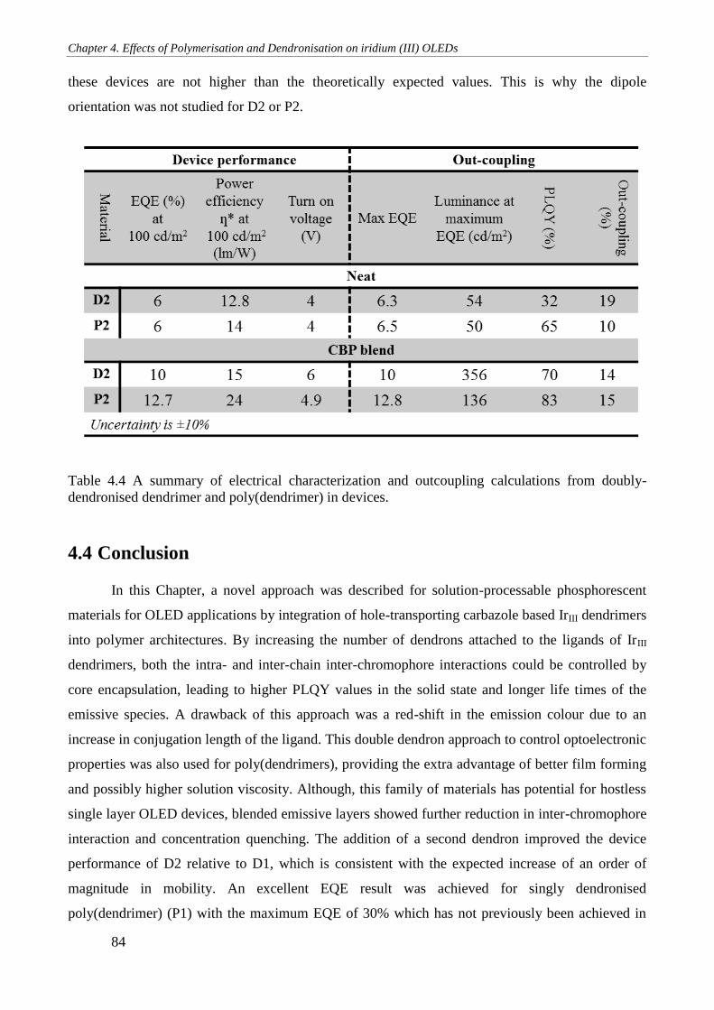
Chapter 4. Effects of Polymerisation and Dendronisation on iridium (III) OLEDs
84
these devices are not higher than the theoretically expected values. This is why the dipole
orientation was not studied for D2 or P2.
Table 4.4 A summary of electrical characterization and outcoupling calculations from doubly-
dendronised dendrimer and poly(dendrimer) in devices.
4.4 Conclusion
In this Chapter, a novel approach was described for solution-processable phosphorescent
materials for OLED applications by integration of hole-transporting carbazole based IrIII dendrimers
into polymer architectures. By increasing the number of dendrons attached to the ligands of IrIII
dendrimers, both the intra- and inter-chain inter-chromophore interactions could be controlled by
core encapsulation, leading to higher PLQY values in the solid state and longer life times of the
emissive species. A drawback of this approach was a red-shift in the emission colour due to an
increase in conjugation length of the ligand. This double dendron approach to control optoelectronic
properties was also used for poly(dendrimers), providing the extra advantage of better film forming
and possibly higher solution viscosity. Although, this family of materials has potential for hostless
single layer OLED devices, blended emissive layers showed further reduction in inter-chromophore
interaction and concentration quenching. The addition of a second dendron improved the device
performance of D2 relative to D1, which is consistent with the expected increase of an order of
magnitude in mobility. An excellent EQE result was achieved for singly dendronised
poly(dendrimer) (P1) with the maximum EQE of 30% which has not previously been achieved in
Chapter 4. Effects of Polymerisation and Dendronisation on iridium (III) OLEDs
85
solution processed OLEDs. This was evidence for horizontally oriented emissive dipoles in the
singly dendronised dendrimer D1 and poly(dendrimer) P1, observed initially by an out coupling
(25% and 40% respectively) which was higher than the theoretically expected out coupling value
(20%). This is a promising achievement as it allows more efficient OLEDs to be realized via
modifications made to the intrinsic properties of the material.
In the next Chapter, a systematic study on singly dendronised co-polymers containing both
hole- and electron- transporting moieties will be presented in order to investigate the possibility of
achieving more efficient devices by balancing the device charge transport via an ambipolar
material.
Chapter 4. Effects of Polymerisation and Dendronisation on iridium (III) OLEDs
86
References
[1] K. Brunner, A. van Dijken, H. Börner, J.J. Bastiaansen, N.M. Kiggen, B.M. Langeveld,
Carbazole compounds as host materials for triplet emitters in organic light-emitting diodes: tuning
the HOMO level without influencing the triplet energy in small molecules, Journal of the American
Chemical Society, 126 (2004) 6035-6042.
[2] A. van Dijken, J.J. Bastiaansen, N.M. Kiggen, B.M. Langeveld, C. Rothe, A. Monkman, I.
Bach, P. Stössel, K. Brunner, Carbazole compounds as host materials for triplet emitters in organic
light-emitting diodes: polymer hosts for high-efficiency light-emitting diodes, Journal of the
American Chemical Society, 126 (2004) 7718-7727.
[3] J. Ding, J. Gao, Y. Cheng, Z. Xie, L. Wang, D. Ma, X. Jing, F. Wang, Highly Efficient Green‐Emitting Phosphorescent Iridium Dendrimers Based on Carbazole Dendrons, Advanced Functional
Materials, 16 (2006) 575-581.
[4] K.A. Knights, S.G. Stevenson, C.P. Shipley, S.-C. Lo, S. Olsen, R.E. Harding, S. Gambino, P.L.
Burn, I.D. Samuel, A rapid route to carbazole containing dendrons and phosphorescent dendrimers,
Journal of Materials Chemistry, 18 (2008) 2121-2130.
[5] J. Ding, J. Lü, Y. Cheng, Z. Xie, L. Wang, X. Jing, F. Wang, Solution‐Processible Red Iridium
Dendrimers based on Oligocarbazole Host Dendrons: Synthesis, Properties, and their Applications
in Organic Light‐Emitting Diodes, Advanced Functional Materials, 18 (2008) 2754-2762.
[6] S.-C. Lo, E. Namdas, P. Burn, I. Samuel, Synthesis and properties of highly efficient
electroluminescent green phosphorescent iridium cored dendrimers, Macromolecules, 36 (2003)
9721-9730.
[7] J. Lupton, I. Samuel, R. Beavington, M. Frampton, P. Burn, H. Bässler, Control of mobility in
molecular organic semiconductors by dendrimer generation, Physical Review B, 63 (2001) 155206.
[8] J.P. Markham, I.D. Samuel, S.-C. Lo, P.L. Burn, M. Weiter, H. Bässler, Charge transport in
highly efficient iridium cored electrophosphorescent dendrimers, Journal of applied physics, 95
(2004) 438-445.
[9] S.C. Lo, T.D. Anthopoulos, E.B. Namdas, P.L. Burn, I.D. Samuel, Encapsulated Cores: Host‐Free Organic Light‐Emitting Diodes Based on Solution‐Processible Electrophosphorescent
Dendrimers, Advanced materials, 17 (2005) 1945-1948.
[10] J. Markham, S.-C. Lo, S. Magennis, P. Burn, I. Samuel, High-efficiency green
phosphorescence from spin-coated single-layer dendrimer light-emitting diodes, Applied physics
letters, 80 (2002) 2645-2647.
[11] S.C. Lo, R.N. Bera, R.E. Harding, P.L. Burn, I.D. Samuel, Solution‐Processible
Phosphorescent Blue Dendrimers Based on Biphenyl‐Dendrons and Fac‐tris (phenyltriazolyl)
iridium (III) Cores, Advanced Functional Materials, 18 (2008) 3080-3090.
[12] S. Gambino, S.C. Lo, Z. Liu, P.L. Burn, I.D. Samuel, Charge Transport in a Highly
Phosphorescent Iridium (III) Complex‐Cored Dendrimer with Double Dendrons, Advanced
Functional Materials, 22 (2012) 157-165.
[13] W.-Y. Lai, J.W. Levell, M.N. Balfour, P.L. Burn, S.-C. Lo, I.D. Samuel, The ‘double
dendron’approach to host free phosphorescent poly (dendrimer) OLEDs, Polymer Chemistry, 3
(2012) 734-740.
[14] T. Shimoda, K. Morii, S. Seki, H. Kiguchi, Inkjet printing of light-emitting polymer displays,
Mrs Bulletin, 28 (2003) 821-827.
[15] M. Singh, H.M. Haverinen, P. Dhagat, G.E. Jabbour, Inkjet printing-process and its
applications, Advanced materials, 22 (2010) 673.
[16] J.P. Gunning, J.W. Levell, M.F. Wyatt, P.L. Burn, J. Robertson, I.D. Samuel, The development
of poly (dendrimer) s for advanced processing, Polymer Chemistry, 1 (2010) 730-738.
[17] W.-Y. Lai, M.N. Balfour, J.W. Levell, A.K. Bansal, P.L. Burn, S.-C. Lo, I.D. Samuel, Poly
(dendrimers) with phosphorescent iridium (III) complex-based side chains prepared via ring-
opening metathesis polymerization, Macromolecules, 45 (2012) 2963-2971.
Chapter 4. Effects of Polymerisation and Dendronisation on iridium (III) OLEDs
87
[18] W.-Y. Lai, J.W. Levell, A.C. Jackson, S.-C. Lo, P.V. Bernhardt, I.D. Samuel, P.L. Burn, A
phosphorescent poly (dendrimer) containing iridium (III) complexes: synthesis and light-emitting
properties, Macromolecules, 43 (2010) 6986-6994.
[19] K.O. Kim, T.-L. Choi, Synthesis of Dendronized Polymers via Macromonomer Approach by
Living ROMP and Their Characterization: From Rod-Like Homopolymers to Block and Gradient
Copolymers, Macromolecules, 46 (2013) 5905-5914.
[20] K.O. Kim, T.-L. Choi, Synthesis of rod-like dendronized polymers containing G4 and G5 ester
dendrons via macromonomer approach by living ROMP, ACS Macro Letters, 1 (2012) 445-448.
[21] X. Chen, J.-L. Liao, Y. Liang, M. Ahmed, H.-E. Tseng, S.-A. Chen, High-efficiency red-light
emission from polyfluorenes grafted with cyclometalated iridium complexes and charge transport
moiety, Journal of the American Chemical Society, 125 (2003) 636-637.
[22] N.R. Evans, L. Sudha Devi, C.S. Mak, S.E. Watkins, S.I. Pascu, A. Köhler, R.H. Friend, C.K.
Williams, A.B. Holmes, Triplet energy back transfer in conjugated polymers with pendant
phosphorescent iridium complexes, Journal of the American Chemical Society, 128 (2006) 6647-
6656.
[23] V. Jankus, C. Winscom, A.P. Monkman, The photophysics of singlet, triplet, and degradation
trap states in 4, 4-N, N′-dicarbazolyl-1, 1′-biphenyl, The Journal of chemical physics, 130 (2009)
074501.
[24] W. Brütting, J. Frischeisen, T.D. Schmidt, B.J. Scholz, C. Mayr, Device efficiency of organic
light‐emitting diodes: Progress by improved light outcoupling, physica status solidi (a), 210 (2013)
44-65.
[25] Y. Sakai, M. Shibata, D. Yokoyama, Simple model-free estimation of orientation order
parameters of vacuum-deposited and spin-coated amorphous films used in organic light-emitting
diodes, Applied Physics Express, 8 (2015) 096601.
[26] L. Zhao, T. Komino, M. Inoue, J.-H. Kim, J.C. Ribierre, C. Adachi, Horizontal molecular
orientation in solution-processed organic light-emitting diodes, Applied Physics Letters, 106 (2015)
063301.
[27] C.-K. Moon, K.-H. Kim, J.W. Lee, J.-J. Kim, Influence of host molecules on emitting dipole
orientation of phosphorescent iridium complexes, Chemistry of Materials, 27 (2015) 2767-2769.
[28] M.J. Jurow, C. Mayr, T.D. Schmidt, T. Lampe, P.I. Djurovich, W. Brütting, M.E. Thompson,
Understanding and predicting the orientation of heteroleptic phosphors in organic light-emitting
materials, Nature materials, (2015).
[29] C. Adachi, M.A. Baldo, S.R. Forrest, M.E. Thompson, High-efficiency organic
electrophosphorescent devices with tris (2-phenylpyridine) iridium doped into electron-transporting
materials, Applied Physics Letters, 77 (2000) 904.
[30] E.B. Namdas, A. Ruseckas, I.D. Samuel, S.-C. Lo, P.L. Burn, Photophysics of fac-tris (2-
phenylpyridine) iridium (III) cored electroluminescent dendrimers in solution and films, The
Journal of Physical Chemistry B, 108 (2004) 1570-1577.
[31] S. Gambino, S.G. Stevenson, K.A. Knights, P.L. Burn, I.D. Samuel, Control of Charge
Transport in Iridium (III) Complex‐Cored Carbazole Dendrimers by Generation and Structural
Modification, Advanced Functional Materials, 19 (2009) 317-323.
[32] P. Wolfer, A. Armin, A. Pivrikas, M. Velusamy, P.L. Burn, P. Meredith, Solution structure:
defining polymer film morphology and optoelectronic device performance, J. Mater. Chem. C, 2
(2013) 71-77.
[33] A. Armin, P. Wolfer, P.E. Shaw, M. Hambsch, F. Maasoumi, M. Ullah, E. Gann, C.R.
McNeill, J. Li, Z. Shi, Simultaneous enhancement of charge generation quantum yield and carrier
transport in organic solar cells, Journal of Materials Chemistry C, 3 (2015) 10799-10812.
[34] S.G. Stevenson, Dendrimer light-emitting diodes, in, University of St Andrews, 2008.
88
Chapter 5
Ambipolar Poly(dendrimer) OLEDs
5.1 Introduction
Phosphorescent poly(dendrimers) have the potential to be applied in large area OLED
display applications because of their efficient photo-physical properties and solution processability.
Their solution processability provides engineering advantages so that film deposition can be
achieved via wet processes such as large area screen or ink-jet printing. In the previous chapter,
poly(dendrimers) containing a carbazole moiety as the hole transport dendron showed promising
device performance. However, to achieve the necessary high device efficiencies, it would be ideal
to develop ambipolar polymeric materials that contain both an electron- and hole- transporting
moiety to improve recombination efficiency.
Several reports have shown the beneficial effects of doping polymeric hole transport
materials with oxadiazole electron transport molecules [1, 2]. Combinations of carbazole and
oxadiazole derivatives have also been shown to be widely used as a suitable choice for ambipolar
host materials. There are different approaches to incorporate both moieties: blends of small
molecule or polymeric derivatives of oxadiazole with polymeric carbazole derivatives[3-8], host
polymers with a carbazole backbone and oxadiazole pendants[9], block and random copolymers of
carbazole and oxadiazole based monomers as a host material[10], and conjugated or non-conjugated
host molecules of carbazole and oxadiazole moieties[11-15] for example.
On the other hand, blending two host materials or an ambipolar host material with a
phosphorescent iridium complex can lead to phase separation. To address this issue, single co-
polymers containing carbazole and oxadiazole moieties and a phosphorescent iridium complex were
designed to retain both charge transport (electron and hole) and triplet harvesting properties. This
chapter contains photo-physical and OLED device characterization of the block co-polymer and
random copolymer containing carbazole and oxadiazole moieties.
Chapter5. Ambipolar Poly(dendrimers) OLEDs
89
5.2 Material design and experimental methods
Figure 5.1.a and b show the block co-polymer (B) and random co-polymer (R) that were
used in the work described in this chapter. These two materials have the same chemical units
consisting of a phosphorescent iridium complex with a carbazole dendron and an oxadiazole unit (in
pink), both directly attached to a non-conjugated polymer back bone. In block co-polymer (B)
alternating sections of the polymer chain consist of either all oxadiazole units or the iridium core
with carbazole dendrons. However, in the random co-polymer (R) the oxadiazole and iridium
core/carbazole units are attached to the polymer back bone completely randomly. In addition, two
small molecules commercially available from Lumtec, 4,4’-N,N’-dicarbazolyl-biphenyl (CBP) and
2,2',2"-(1,3,5-Benzinetriyl)-tris(1-phenyl-1-H-benzimidazole) (TPBi) were used as a host and
electron transport materials, respectively. The structure of these can be seen in Chapter 3, Figure
3.1.b and c.
The photo-physical characterisation was performed on degassed optically dilute solutions
and solid state films (neat and blend) as detailed in Chapter 2. Neat films were spin cast from a 15
mg/ml and 18 mg/ml concentrations respectively for B and R compounds, while for blends the
dopant ratio was 20 wt%. The thicknesses of the solid state samples for photophysical testing were
identical to those used in devices. Due to their high molecular weight, both co-polymers were
stirred into the solvent overnight prior to the deposition to ensure they had fully dissolved.
Devices (see Figure 5.2.a) were fabricated on pre-patterned ITO substrates with 170 nm of
ITO thickness and 10 Ω/sq sheet resistance. Substrates were pre-cleaned with isopropanol and DI
water and then treated with UV-ozone for 15 minutes at 25°C immediately prior to the deposition of
next layer. A 30nm PEDOT:PSS film was then deposited and annealed for 15min at 150° C. The
PEDOT:PSS was used to ease the injection according to the energy level diagram (see Figure
5.2.b). Devices were then transferred into a nitrogen-filled glovebox where the emissive layers (neat
or blend) were deposited on the substrates by spin-coating (2100 rpm) from the overnight stirred
solutions. The film thickness (~ 70-80 nm) used in photo-physical characterisation was used in
device fabrication. Chlorobenzene and chloroform were used as the solvents for these devices for
neat and blend films, respectively.
Finally, successive layers of TPBi (35 nm), LiF, and Al were deposited using thermal
evaporation through shadow masks in a vacuum chamber under a base pressure of around 5 ×
10−6mbar. The deposition rate for the TPBi layer was maintained at approximately 1 Å/s. The
cathode layers, LiF (1 nm) and Al (100 nm), were then sequentially deposited without breaking the
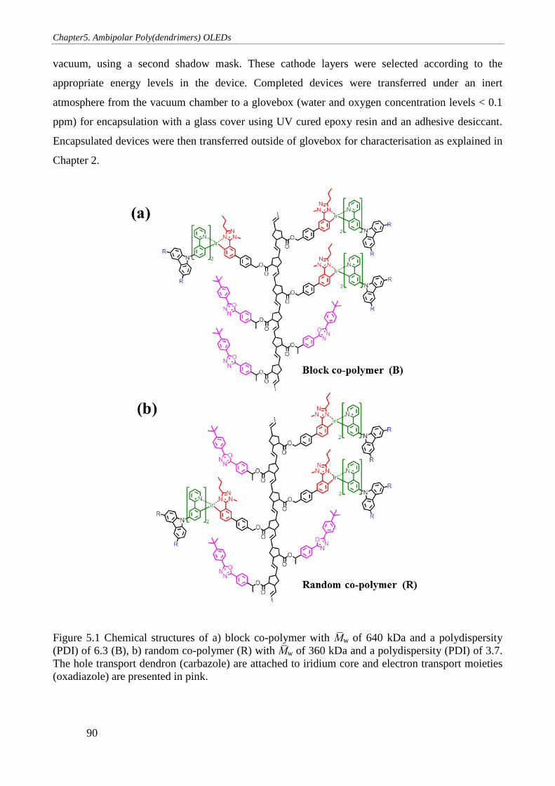
Chapter5. Ambipolar Poly(dendrimers) OLEDs
90
vacuum, using a second shadow mask. These cathode layers were selected according to the
appropriate energy levels in the device. Completed devices were transferred under an inert
atmosphere from the vacuum chamber to a glovebox (water and oxygen concentration levels < 0.1
ppm) for encapsulation with a glass cover using UV cured epoxy resin and an adhesive desiccant.
Encapsulated devices were then transferred outside of glovebox for characterisation as explained in
Chapter 2.
Figure 5.1 Chemical structures of a) block co-polymer with M̅w of 640 kDa and a polydispersity
(PDI) of 6.3 (B), b) random co-polymer (R) with M̅w of 360 kDa and a polydispersity (PDI) of 3.7.
The hole transport dendron (carbazole) are attached to iridium core and electron transport moieties
(oxadiazole) are presented in pink.
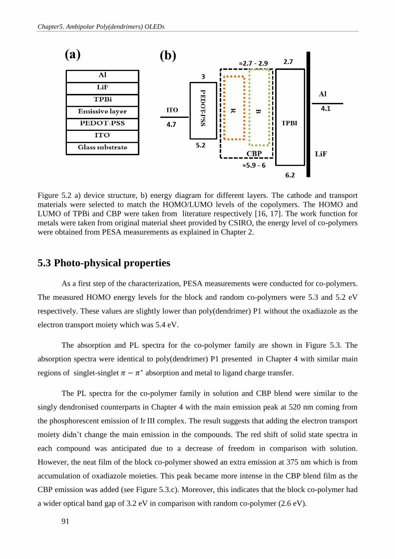
Chapter5. Ambipolar Poly(dendrimers) OLEDs
91
Figure 5.2 a) device structure, b) energy diagram for different layers. The cathode and transport
materials were selected to match the HOMO/LUMO levels of the copolymers. The HOMO and
LUMO of TPBi and CBP were taken from literature respectively [16, 17]. The work function for
metals were taken from original material sheet provided by CSIRO, the energy level of co-polymers
were obtained from PESA measurements as explained in Chapter 2.
5.3 Photo-physical properties
As a first step of the characterization, PESA measurements were conducted for co-polymers.
The measured HOMO energy levels for the block and random co-polymers were 5.3 and 5.2 eV
respectively. These values are slightly lower than poly(dendrimer) P1 without the oxadiazole as the
electron transport moiety which was 5.4 eV.
The absorption and PL spectra for the co-polymer family are shown in Figure 5.3. The
absorption spectra were identical to poly(dendrimer) P1 presented in Chapter 4 with similar main
regions of singlet-singlet 𝜋 − 𝜋∗ absorption and metal to ligand charge transfer.
The PL spectra for the co-polymer family in solution and CBP blend were similar to the
singly dendronised counterparts in Chapter 4 with the main emission peak at 520 nm coming from
the phosphorescent emission of Ir III complex. The result suggests that adding the electron transport
moiety didn’t change the main emission in the compounds. The red shift of solid state spectra in
each compound was anticipated due to a decrease of freedom in comparison with solution.
However, the neat film of the block co-polymer showed an extra emission at 375 nm which is from
accumulation of oxadiazole moieties. This peak became more intense in the CBP blend film as the
CBP emission was added (see Figure 5.3.c). Moreover, this indicates that the block co-polymer had
a wider optical band gap of 3.2 eV in comparison with random co-polymer (2.6 eV).
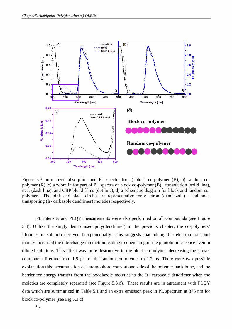
Chapter5. Ambipolar Poly(dendrimers) OLEDs
92
Figure 5.3 normalized absorption and PL spectra for a) block co-polymer (B), b) random co-
polymer (R), c) a zoom in for part of PL spectra of block co-polymer (B), for solution (solid line),
neat (dash line), and CBP blend films (dot line), d) a schematic diagram for block and random co-
polymers. The pink and black circles are representative for electron (oxadiazole) - and hole-
transporting (Ir- carbazole dendrimer) moieties respectively.
PL intensity and PLQY measurements were also performed on all compounds (see Figure
5.4). Unlike the singly dendronised poly(dendrimer) in the previous chapter, the co-polymers’
lifetimes in solution decayed biexponentially. This suggests that adding the electron transport
moiety increased the interchange interaction leading to quenching of the photoluminescence even in
diluted solutions. This effect was more destructive in the block co-polymer decreasing the slower
component lifetime from 1.5 µs for the random co-polymer to 1.2 µs. There were two possible
explanation this; accumulation of chromophore cores at one side of the polymer back bone, and the
barrier for energy transfer from the oxadiazole moieties to the Ir- carbazole dendrimer when the
moieties are completely separated (see Figure 5.3.d). These results are in agreement with PLQY
data which are summarized in Table 5.1 and an extra emission peak in PL spectrum at 375 nm for
block co-polymer (see Fig 5.3.c)
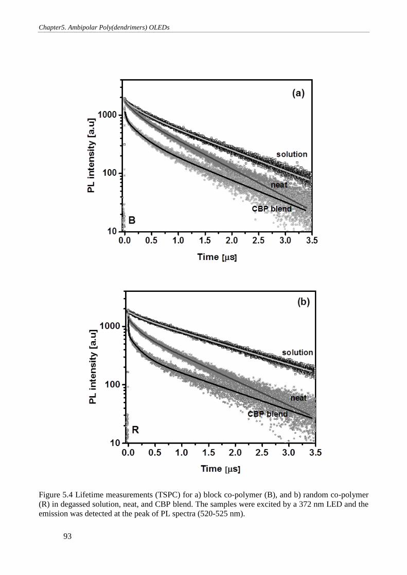
Chapter5. Ambipolar Poly(dendrimers) OLEDs
93
Figure 5.4 Lifetime measurements (TSPC) for a) block co-polymer (B), and b) random co-polymer
(R) in degassed solution, neat, and CBP blend. The samples were excited by a 372 nm LED and the
emission was detected at the peak of PL spectra (520-525 nm).
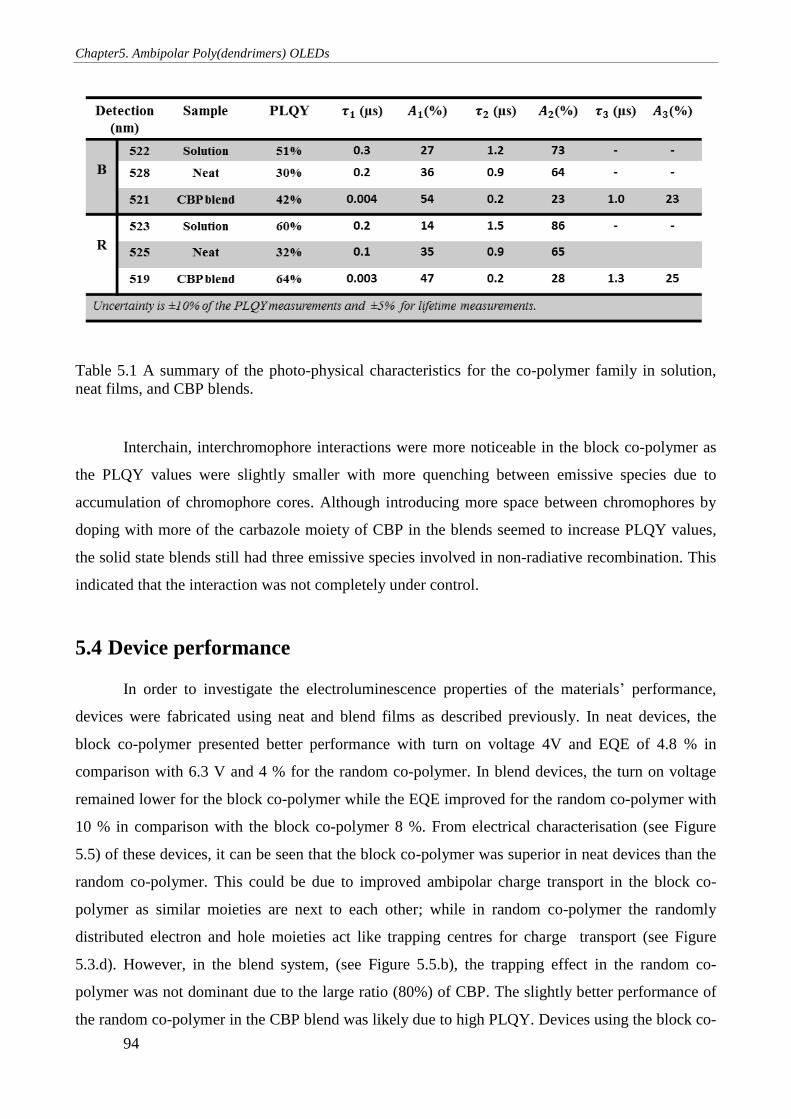
Chapter5. Ambipolar Poly(dendrimers) OLEDs
94
Table 5.1 A summary of the photo-physical characteristics for the co-polymer family in solution,
neat films, and CBP blends.
Interchain, interchromophore interactions were more noticeable in the block co-polymer as
the PLQY values were slightly smaller with more quenching between emissive species due to
accumulation of chromophore cores. Although introducing more space between chromophores by
doping with more of the carbazole moiety of CBP in the blends seemed to increase PLQY values,
the solid state blends still had three emissive species involved in non-radiative recombination. This
indicated that the interaction was not completely under control.
5.4 Device performance
In order to investigate the electroluminescence properties of the materials’ performance,
devices were fabricated using neat and blend films as described previously. In neat devices, the
block co-polymer presented better performance with turn on voltage 4V and EQE of 4.8 % in
comparison with 6.3 V and 4 % for the random co-polymer. In blend devices, the turn on voltage
remained lower for the block co-polymer while the EQE improved for the random co-polymer with
10 % in comparison with the block co-polymer 8 %. From electrical characterisation (see Figure
5.5) of these devices, it can be seen that the block co-polymer was superior in neat devices than the
random co-polymer. This could be due to improved ambipolar charge transport in the block co-
polymer as similar moieties are next to each other; while in random co-polymer the randomly
distributed electron and hole moieties act like trapping centres for charge transport (see Figure
5.3.d). However, in the blend system, (see Figure 5.5.b), the trapping effect in the random co-
polymer was not dominant due to the large ratio (80%) of CBP. The slightly better performance of
the random co-polymer in the CBP blend was likely due to high PLQY. Devices using the block co-
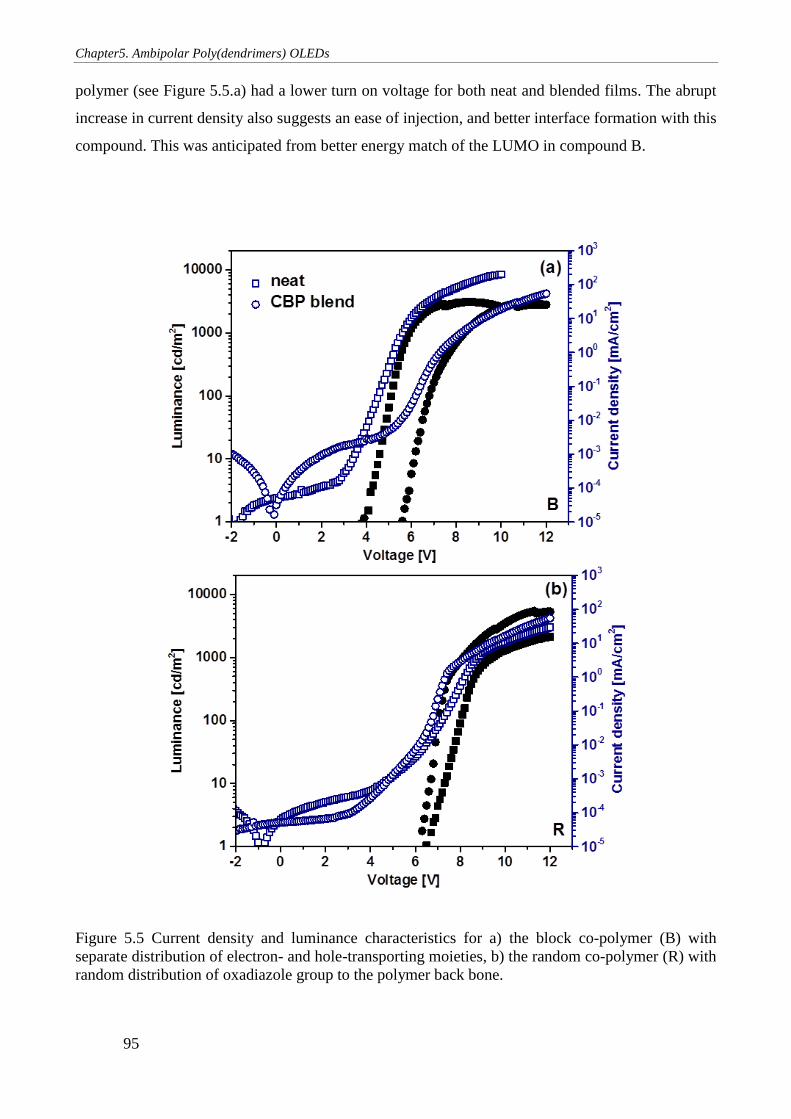
Chapter5. Ambipolar Poly(dendrimers) OLEDs
95
polymer (see Figure 5.5.a) had a lower turn on voltage for both neat and blended films. The abrupt
increase in current density also suggests an ease of injection, and better interface formation with this
compound. This was anticipated from better energy match of the LUMO in compound B.
Figure 5.5 Current density and luminance characteristics for a) the block co-polymer (B) with
separate distribution of electron- and hole-transporting moieties, b) the random co-polymer (R) with
random distribution of oxadiazole group to the polymer back bone.
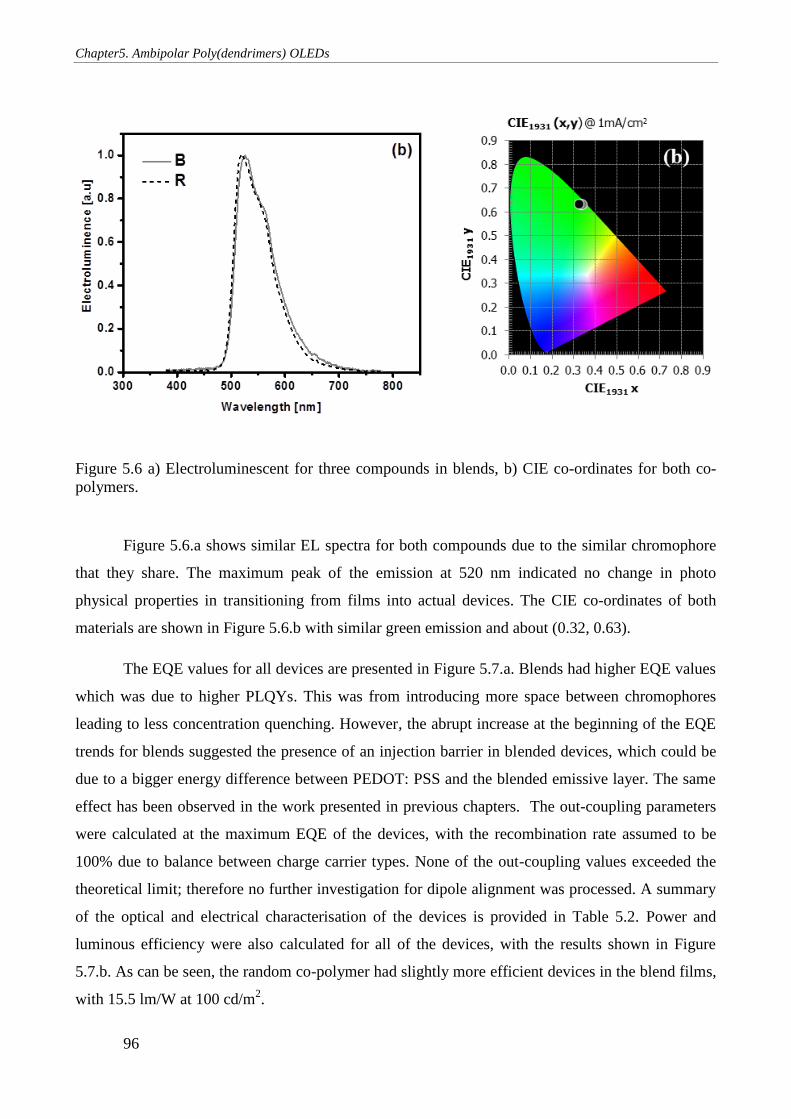
Chapter5. Ambipolar Poly(dendrimers) OLEDs
96
Figure 5.6 a) Electroluminescent for three compounds in blends, b) CIE co-ordinates for both co-
polymers.
Figure 5.6.a shows similar EL spectra for both compounds due to the similar chromophore
that they share. The maximum peak of the emission at 520 nm indicated no change in photo
physical properties in transitioning from films into actual devices. The CIE co-ordinates of both
materials are shown in Figure 5.6.b with similar green emission and about (0.32, 0.63).
The EQE values for all devices are presented in Figure 5.7.a. Blends had higher EQE values
which was due to higher PLQYs. This was from introducing more space between chromophores
leading to less concentration quenching. However, the abrupt increase at the beginning of the EQE
trends for blends suggested the presence of an injection barrier in blended devices, which could be
due to a bigger energy difference between PEDOT: PSS and the blended emissive layer. The same
effect has been observed in the work presented in previous chapters. The out-coupling parameters
were calculated at the maximum EQE of the devices, with the recombination rate assumed to be
100% due to balance between charge carrier types. None of the out-coupling values exceeded the
theoretical limit; therefore no further investigation for dipole alignment was processed. A summary
of the optical and electrical characterisation of the devices is provided in Table 5.2. Power and
luminous efficiency were also calculated for all of the devices, with the results shown in Figure
5.7.b. As can be seen, the random co-polymer had slightly more efficient devices in the blend films,
with 15.5 lm/W at 100 cd/m2.
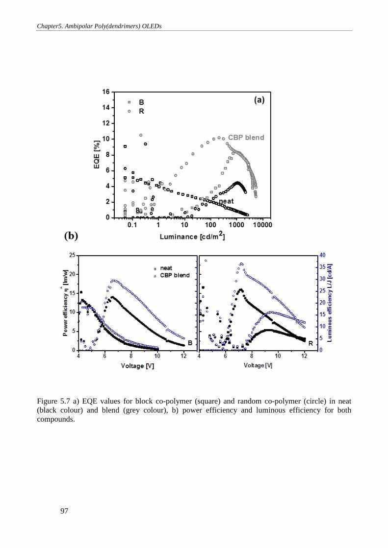
Chapter5. Ambipolar Poly(dendrimers) OLEDs
97
Figure 5.7 a) EQE values for block co-polymer (square) and random co-polymer (circle) in neat
(black colour) and blend (grey colour), b) power efficiency and luminous efficiency for both
compounds.
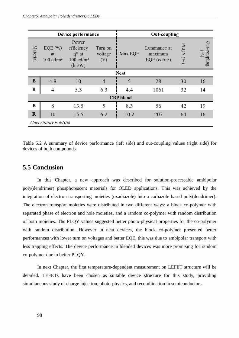
Chapter5. Ambipolar Poly(dendrimers) OLEDs
98
Table 5.2 A summary of device performance (left side) and out-coupling values (right side) for
devices of both compounds.
5.5 Conclusion
In this Chapter, a new approach was described for solution-processable ambipolar
poly(dendrimer) phosphorescent materials for OLED applications. This was achieved by the
integration of electron-transporting moieties (oxadiazole) into a carbazole based poly(dendrimer).
The electron transport moieties were distributed in two different ways: a block co-polymer with
separated phase of electron and hole moieties, and a random co-polymer with random distribution
of both moieties. The PLQY values suggested better photo-physical properties for the co-polymer
with random distribution. However in neat devices, the block co-polymer presented better
performances with lower turn on voltages and better EQE, this was due to ambipolar transport with
less trapping effects. The device performance in blended devices was more promising for random
co-polymer due to better PLQY.
In next Chapter, the first temperature-dependent measurement on LEFET structure will be
detailed. LEFETs have been chosen as suitable device structure for this study, providing
simultaneous study of charge injection, photo-physics, and recombination in semiconductors.
Chapter5. Ambipolar Poly(dendrimers) OLEDs
99
References:
[1] C. Jiang, W. Yang, J. Peng, S. Xiao, Y. Cao, High‐efficiency, saturated red‐phosphorescent
polymer light‐emitting diodes based on conjugated and non‐conjugated polymers doped with an Ir
complex, Advanced Materials, 16 (2004) 537-541.
[2] X. Gong, M.R. Robinson, J.C. Ostrowski, D. Moses, G.C. Bazan, A.J. Heeger, High‐Efficiency
Polymer‐Based Electrophosphorescent Devices, Advanced Materials, 14 (2002) 581-585.
[3] C. Adachi, R. Kwong, S.R. Forrest, Efficient electrophosphorescence using a doped ambipolar
conductive molecular organic thin film, Organic Electronics, 2 (2001) 37-43.
[4] S. Lamansky, P.I. Djurovich, F. Abdel-Razzaq, S. Garon, D.L. Murphy, M.E. Thompson,
Cyclometalated Ir complexes in polymer organic light-emitting devices, Journal of applied physics,
92 (2002) 1570-1575.
[5] X. Yang, F. Jaiser, S. Klinger, D. Neher, Blue polymer electrophosphorescent devices with
different electron-transporting oxadiazoles, Applied physics letters, 88 (2006) 021107.
[6] X. Yang, D. Muller, D. Neher, K. Meerholz, Highly efficient polymeric electrophosphorescent
diodes, Advanced Materials, 18 (2006) 948-954.
[7] K. Zhang, Z. Chen, C. Yang, X. Zhang, Y. Tao, L. Duan, L. Chen, L. Zhu, J. Qin, Y. Cao,
Improving the performance of phosphorescent polymer light-emitting diodes using morphology-
stable carbazole-based iridium complexes, Journal of Materials Chemistry, 17 (2007) 3451-3460.
[8] S.-J. Kim, Y. Zhang, C. Zuniga, S. Barlow, S.R. Marder, B. Kippelen, Efficient green OLED
devices with an emissive layer comprised of phosphor-doped carbazole/bis-oxadiazole side-chain
polymer blends, Organic Electronics, 12 (2011) 492-496.
[9] K. Zhang, Y. Tao, C. Yang, H. You, Y. Zou, J. Qin, D. Ma, Synthesis and properties of
carbazole main chain copolymers with oxadiazole pendant toward bipolar polymer host: tuning the
HOMO/LUMO level and triplet energy, Chemistry of Materials, 20 (2008) 7324-7331.
[10] L. Deng, P.T. Furuta, S. Garon, J. Li, D. Kavulak, M.E. Thompson, J.M. Fréchet, Living
radical polymerization of bipolar transport materials for highly efficient light emitting diodes,
Chemistry of materials, 18 (2006) 386-395.
[11] M. Guan, Z. Chen, Z. Bian, Z. Liu, Z. Gong, W. Baik, H. Lee, C. Huang, The host materials
containing carbazole and oxadiazole fragment for red triplet emitter in organic light-emitting
diodes, Organic electronics, 7 (2006) 330-336.
[12] M.-k. Leung, C.-C. Yang, J.-H. Lee, H.-H. Tsai, C.-F. Lin, C.-Y. Huang, Y.O. Su, C.-F. Chiu,
The unusual electrochemical and photophysical behavior of 2, 2'-bis (1, 3, 4-oxadiazol-2-yl)
biphenyls, effective electron transport hosts for phosphorescent organic light emitting diodes,
Organic letters, 9 (2007) 235-238.
[13] Y. Tao, Q. Wang, C. Yang, Q. Wang, Z. Zhang, T. Zou, J. Qin, D. Ma, A simple
carbazole/oxadiazole hybrid molecule: an excellent bipolar host for green and red phosphorescent
OLEDs, Angewandte Chemie, 120 (2008) 8224-8227.
[14] Y. Tao, Q. Wang, C. Yang, C. Zhong, K. Zhang, J. Qin, D. Ma, Tuning the optoelectronic
properties of carbazole/oxadiazole hybrids through linkage modes: hosts for highly efficient green
electrophosphorescence, Advanced Functional Materials, 20 (2010) 304-311.
[15] Y. Zhang, W. Haske, D. Cai, S. Barlow, B. Kippelen, S.R. Marder, Efficient blue-emitting
electrophosphorescent organic light-emitting diodes using 2-(3, 5-di (carbazol-9-yl) phenyl)-5-
phenyl-1, 3, 4-oxadiazole as an ambipolar host, RSC Advances, 3 (2013) 23514-23520.
[16] Y. Tao, C. Yang, J. Qin, Organic host materials for phosphorescent organic light-emitting
diodes, Chemical Society Reviews, 40 (2011) 2943-2970.
[17] H. Fukagawa, K. Watanabe, S. Tokito, Efficient white organic light emitting diodes with
solution processed and vacuum deposited emitting layers, Organic Electronics, 10 (2009) 798-802.
100
Chapter 6
Charge Transport and Recombination in
Heterostructure Organic Light Emitting
Transistors
6.1 Introduction
Organic light-emitting field effect transistors are dual function devices in that they have the
electroluminescence capabilities of organic light-emitting diodes plus the switching capabilities of a
field effect transistor in a single architecture [1-5]. This dual functionality can potentially lead to
new applications such as simplified pixels for flat panel displays and potentially an electrical driven
organic semiconductor laser. Although the emission brightness of LEFETs has improved over the
last decade [6-17], their electrical switching ON/OFF ratio and EQE at high brightness are still very
much sub-optimal. This is in part due to a lack of knowledge with respect to materials design and
the absence of a comprehensive understanding of the charge transport and radiative recombination
processes that occur in a LEFET.
A common method to probe the charge transport in organic semiconductor films is to
measure the optoelectronic characteristics of the material as a function of temperature in a FET or
diode configuration [18-24]. Specifically, in the diode configuration both transient (e.g., Time-of-
Flight [25], photo-Charge Extraction in Linearly Increasing Voltage [photo-CELIV] [26]) and
steady-state measurements (e.g., Space Charge Limited Current [SCLC]) have been used to
measure mobility and recombination. Recently, Armin et al. reported an adapted injection-CELIV
technique called MIS-CELIV which is capable of measuring the mobility of both carrier types in
diode architectures relevant to operational devices such as solar cells and photodiodes [27].
However, in a functional OLED, it needs to be simultaneously probe not only the transport
properties, but also the recombination dynamics (radiative and non-radiative). Thus, the traditional
transport measurement methodologies only uncover at best half the pertinent physics. Furthermore,
these existing techniques require that the injecting contact must be ohmic. Such a requirement is
hard to achieve in an organic diode configuration. In an OFET architecture, the contact resistance at
Chapter6. Charge Transport and Recombination in Heterostructure Organic Light Emitting Transistors
101
the metal organic interface can be completely eliminated by employing four-probes or the
transmission line technique [28-31]. An OFET structure can potentially map multiple elements of
transport such as charge injection at the organic-metal interface, contact resistance and mobility.
However, OFETs are generally not designed to emit light and are thus, like the simple diode, not
suitable for studying radiative and non-radiative recombination processes.
In this Chapter, we simultaneously probe the mobility and injection of carrier types, contact
resistance and radiative recombination all as a function of temperature in a model bilayer LEFET.
As it is typically difficult to find an organic semiconductor material that is highly luminescent and
with high charge carrier mobility a bilayer LEFET architecture, consisting of a highly luminescent
emissive layer (SY) and a separate charge transport layer (DPP-DTT), was employed. The bilayer
LEFETs show decreases in the source-drain current, mobility (both electrons and holes), and
brightness with decreasing the temperature. However, the external quantum efficiency increases by
an order of magnitude at low temperatures. The changes in mobility and current are thermally
activated consistent with the hopping transport characteristics normally associated with disordered
semiconductors. It was thus demonstrated that the increase in EQE at low temperature is
predominately due to an increase in the radiative recombination efficiency.
6.2 Experimental procedure
6.2.1 Device fabrication
Figure 6.1.a shows the device architecture for top-contact, bottom-gate LEFETs. The
devices were fabricated on 400 nm thick SiNx gate dielectric layer, grown by low pressure physical
vapor deposition (LPCVD), on top of a heavily n-doped silicon wafer purchased from Silicon
Quest, International, Inc. After dicing the wafer into 15 x 15 mm substrates, they were cleaned as
explained in Chapter 2. All remaining fabrication steps and device testing were performed inside a
nitrogen filled MBraun glove box (O2 and H2O levels < 0.1 ppm). The gate dielectric layer was
further passivated with poly (methylmethacrylate) (PMMA) (120,000 gmol) as an organic dielectric
layer. A 35 mg/ml solution of PMMA in n-propylacetate (P99.5%) was spin-coated onto the
substrates at 2500 rpm for 30 s and then 3000 rpm for 10 s. The substrates were then baked on a hot
plate at 150 °C for 30 min. The PMMA film thickness was 120 nm. The materials used for the
semiconducting channel were: an ambipolar diketopyrrolopyrrole-dithienothiophene (DPP-DTT)
co-polymer [32]; and Super Yellow (SY), a phenyl-substituted poly(p-phenylenevinylene) co-
polymer, as the emissive layer. SY (PDY–132) was purchased from Merck and was used without
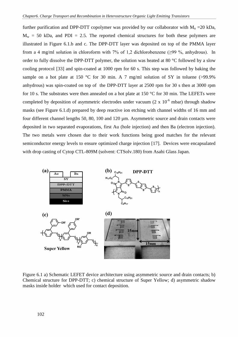
Chapter6. Charge Transport and Recombination in Heterostructure Organic Light Emitting Transistors
102
further purification and DPP-DTT copolymer was provided by our collaborator with Mn =20 kDa,
Mw = 50 kDa, and PDI = 2.5. The reported chemical structures for both these polymers are
illustrated in Figure 6.1.b and c. The DPP-DTT layer was deposited on top of the PMMA layer
from a 4 mg/ml solution in chloroform with 7% of 1,2 dichlorobenzene (≥99 %, anhydrous). In
order to fully dissolve the DPP-DTT polymer, the solution was heated at 80 °C followed by a slow
cooling protocol [33] and spin-coated at 1000 rpm for 60 s. This step was followed by baking the
sample on a hot plate at 150 °C for 30 min. A 7 mg/ml solution of SY in toluene (>99.9%
anhydrous) was spin-coated on top of the DPP-DTT layer at 2500 rpm for 30 s then at 3000 rpm
for 10 s. The substrates were then annealed on a hot plate at 150 °C for 30 min. The LEFETs were
completed by deposition of asymmetric electrodes under vacuum (2 x 10⁻⁶
mbar) through shadow
masks (see Figure 6.1.d) prepared by deep reactive ion etching with channel widths of 16 mm and
four different channel lengths 50, 80, 100 and 120 µm. Asymmetric source and drain contacts were
deposited in two separated evaporations, first Au (hole injection) and then Ba (electron injection).
The two metals were chosen due to their work functions being good matches for the relevant
semiconductor energy levels to ensure optimized charge injection [17]. Devices were encapsulated
with drop casting of Cytop CTL-809M (solvent: CTSolv.180) from Asahi Glass Japan.
Figure 6.1 a) Schematic LEFET device architecture using asymmetric source and drain contacts; b)
Chemical structure for DPP-DTT; c) chemical structure of Super Yellow; d) asymmetric shadow
masks inside holder which used for contact deposition.
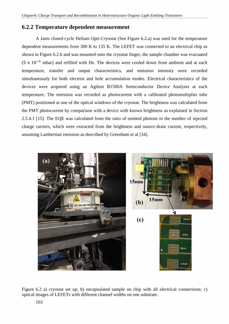
Chapter6. Charge Transport and Recombination in Heterostructure Organic Light Emitting Transistors
103
6.2.2 Temperature dependent measurement
A Janis closed-cycle Helium Opti-Cryostat (See Figure 6.2.a) was used for the temperature
dependent measurements from 300 K to 135 K. The LEFET was connected to an electrical chip as
shown in Figure 6.2.b and was mounted onto the cryostat finger, the sample chamber was evacuated
(5 × 10⁻⁵ mbar) and refilled with He. The devices were cooled down from ambient and at each
temperature, transfer and output characteristics, and emission intensity were recorded
simultaneously for both electron and hole accumulation modes. Electrical characteristics of the
devices were acquired using an Agilent B1500A Semiconductor Device Analyser at each
temperature. The emission was recorded as photocurrent with a calibrated photomultiplier tube
(PMT) positioned at one of the optical windows of the cryostat. The brightness was calculated from
the PMT photocurrent by comparison with a device with known brightness as explained in Section
2.5.4.1 [15]. The EQE was calculated from the ratio of emitted photons to the number of injected
charge carriers, which were extracted from the brightness and source-drain current, respectively,
assuming Lambertian emission as described by Greenham et al [34].
Figure 6.2 a) cryostat set up; b) encapsulated sample on chip with all electrical connections; c)
optical images of LEFETs with different channel widths on one substrate.
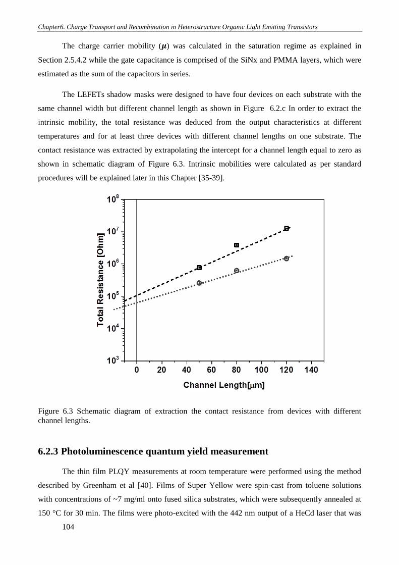
Chapter6. Charge Transport and Recombination in Heterostructure Organic Light Emitting Transistors
104
The charge carrier mobility (𝝁) was calculated in the saturation regime as explained in
Section 2.5.4.2 while the gate capacitance is comprised of the SiNx and PMMA layers, which were
estimated as the sum of the capacitors in series.
The LEFETs shadow masks were designed to have four devices on each substrate with the
same channel width but different channel length as shown in Figure 6.2.c In order to extract the
intrinsic mobility, the total resistance was deduced from the output characteristics at different
temperatures and for at least three devices with different channel lengths on one substrate. The
contact resistance was extracted by extrapolating the intercept for a channel length equal to zero as
shown in schematic diagram of Figure 6.3. Intrinsic mobilities were calculated as per standard
procedures will be explained later in this Chapter [35-39].
Figure 6.3 Schematic diagram of extraction the contact resistance from devices with different
channel lengths.
6.2.3 Photoluminescence quantum yield measurement
The thin film PLQY measurements at room temperature were performed using the method
described by Greenham et al [40]. Films of Super Yellow were spin-cast from toluene solutions
with concentrations of ~7 mg/ml onto fused silica substrates, which were subsequently annealed at
150 °C for 30 min. The films were photo-excited with the 442 nm output of a HeCd laser that was
Chapter6. Charge Transport and Recombination in Heterostructure Organic Light Emitting Transistors
105
attenuated with neutral density filters to ~0.2 mW. The interior of the integrating sphere was
flushed with nitrogen for the duration of the measurement to minimize photodegradation, and the
PL intensity was measured with a calibrated photodiode. The PLQY was measured at 4 points on
the film and the results averaged.
For the temperature-dependent PLQY measurements, the film was placed inside an Oxford
Instruments Optistat DN2 cryostat in a helium atmosphere. The same excitation source was used as
for the room temperature-dependent measurements, although the power incident on the film was
reduced to ~5 μW to minimize damage to the sample from sustained excitation. The films had
absorbance at the excitation wavelength of ~1 so the majority of the incident light was absorbed.
Two detectors were used to monitor the PL signal: a fibre coupled Ocean Optics USB2000
spectrometer, and a Si photodiode. Both were placed close to the sample with a long pass filter
covering the photodiode to block any scattered excitation. The change in PLQY with temperature
was estimated by comparing the relative change in the PL signal intensity between room
temperature and a range of low temperatures. The emission from SY films is not isotropic so the
emission was measured from multiple angles with the results averaged. Furthermore, the
measurements were performed by modulating between high and low temperatures rather than using
a gradient in order to rule out any degradation effects.
6.3 Results and discussions
6.3.1 Room temperature
Figure 6.4.a and b show typical electrical transfer characteristics of the model LEFETs at
room temperature where channel length and width were 50 µm and 16 mm, respectively. The gate
voltage was scanned from -100 V to + 100 V while keeping the source–drain voltage at a fixed
value of -100 V or +100 V. The electrical output characteristics at room temperature are shown in
Figure 6.4.c and d, the devices demonstrated both diode-like and saturation regimes for hole and
electron accumulation [39]. The diode-like characteristics (super-linear increase of drain current
with source-drain voltages) are more prominent in n-channel mode (VG = 0 to 60 V). Further
increase in the gate voltage from 80 V to 100 V leads to accumulation of electrons, and the
transistor operates fully in the n-channel mode. These characteristics are typical of ambipolar
LEFETs [41].
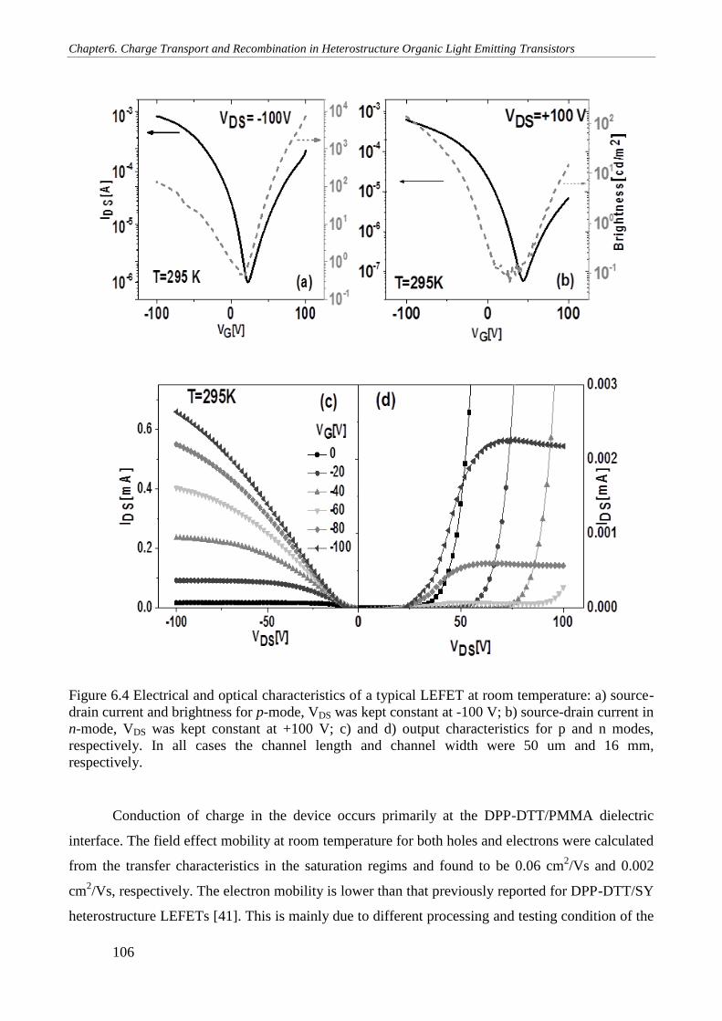
Chapter6. Charge Transport and Recombination in Heterostructure Organic Light Emitting Transistors
106
Figure 6.4 Electrical and optical characteristics of a typical LEFET at room temperature: a) source-
drain current and brightness for p-mode, VDS was kept constant at -100 V; b) source-drain current in
n-mode, VDS was kept constant at +100 V; c) and d) output characteristics for p and n modes,
respectively. In all cases the channel length and channel width were 50 um and 16 mm,
respectively.
Conduction of charge in the device occurs primarily at the DPP-DTT/PMMA dielectric
interface. The field effect mobility at room temperature for both holes and electrons were calculated
from the transfer characteristics in the saturation regims and found to be 0.06 cm2/Vs and 0.002
cm2/Vs, respectively. The electron mobility is lower than that previously reported for DPP-DTT/SY
heterostructure LEFETs [41]. This is mainly due to different processing and testing condition of the
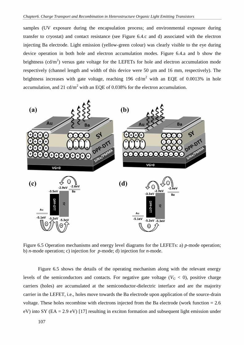
Chapter6. Charge Transport and Recombination in Heterostructure Organic Light Emitting Transistors
107
samples (UV exposure during the encapsulation process; and environmental exposure during
transfer to cryostat) and contact resistance (see Figure 6.4.c and d) associated with the electron
injecting Ba electrode. Light emission (yellow-green colour) was clearly visible to the eye during
device operation in both hole and electron accumulation modes. Figure 6.4.a and b show the
brightness (cd/m2) versus gate voltage for the LEFETs for hole and electron accumulation mode
respectively (channel length and width of this device were 50 µm and 16 mm, respectively). The
brightness increases with gate voltage, reaching 196 cd/m2 with an EQE of 0.0013% in hole
accumulation, and 21 cd/m2 with an EQE of 0.038% for the electron accumulation.
Figure 6.5 Operation mechanisms and energy level diagrams for the LEFETs: a) p-mode operation;
b) n-mode operation; c) injection for p-mode; d) injection for n-mode.
Figure 6.5 shows the details of the operating mechanism along with the relevant energy
levels of the semiconductors and contacts. For negative gate voltage (VG < 0), positive charge
carriers (holes) are accumulated at the semiconductor-dielectric interface and are the majority
carrier in the LEFET, i.e., holes move towards the Ba electrode upon application of the source-drain
voltage. These holes recombine with electrons injected from the Ba electrode (work function = 2.6
eV) into SY (EA = 2.9 eV) [17] resulting in exciton formation and subsequent light emission under
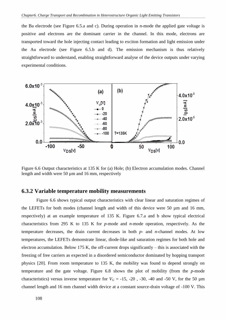
Chapter6. Charge Transport and Recombination in Heterostructure Organic Light Emitting Transistors
108
the Ba electrode (see Figure 6.5.a and c). During operation in n-mode the applied gate voltage is
positive and electrons are the dominant carrier in the channel. In this mode, electrons are
transported toward the hole injecting contact leading to exciton formation and light emission under
the Au electrode (see Figure 6.5.b and d). The emission mechanism is thus relatively
straightforward to understand, enabling straightforward analyse of the device outputs under varying
experimental conditions.
Figure 6.6 Output characteristics at 135 K for (a) Hole; (b) Electron accumulation modes. Channel
length and width were 50 µm and 16 mm, respectively
6.3.2 Variable temperature mobility measurements
Figure 6.6 shows typical output characteristics with clear linear and saturation regimes of
the LEFETs for both modes (channel length and width of this device were 50 µm and 16 mm,
respectively) at an example temperature of 135 K. Figure 6.7.a and b show typical electrical
characteristics from 295 K to 135 K for p-mode and n-mode operation, respectively. As the
temperature decreases, the drain current decreases in both p- and n-channel modes. At low
temperatures, the LEFETs demonstrate linear, diode-like and saturation regimes for both hole and
electron accumulation. Below 175 K, the off-current drops significantly – this is associated with the
freezing of free carriers as expected in a disordered semiconductor dominated by hopping transport
physics [20]. From room temperature to 135 K, the mobility was found to depend strongly on
temperature and the gate voltage. Figure 6.8 shows the plot of mobility (from the p-mode
characteristics) versus inverse temperature for VG = -15, -20 , -30, -40 and -50 V, for the 50 µm
channel length and 16 mm channel width device at a constant source-drain voltage of -100 V. This
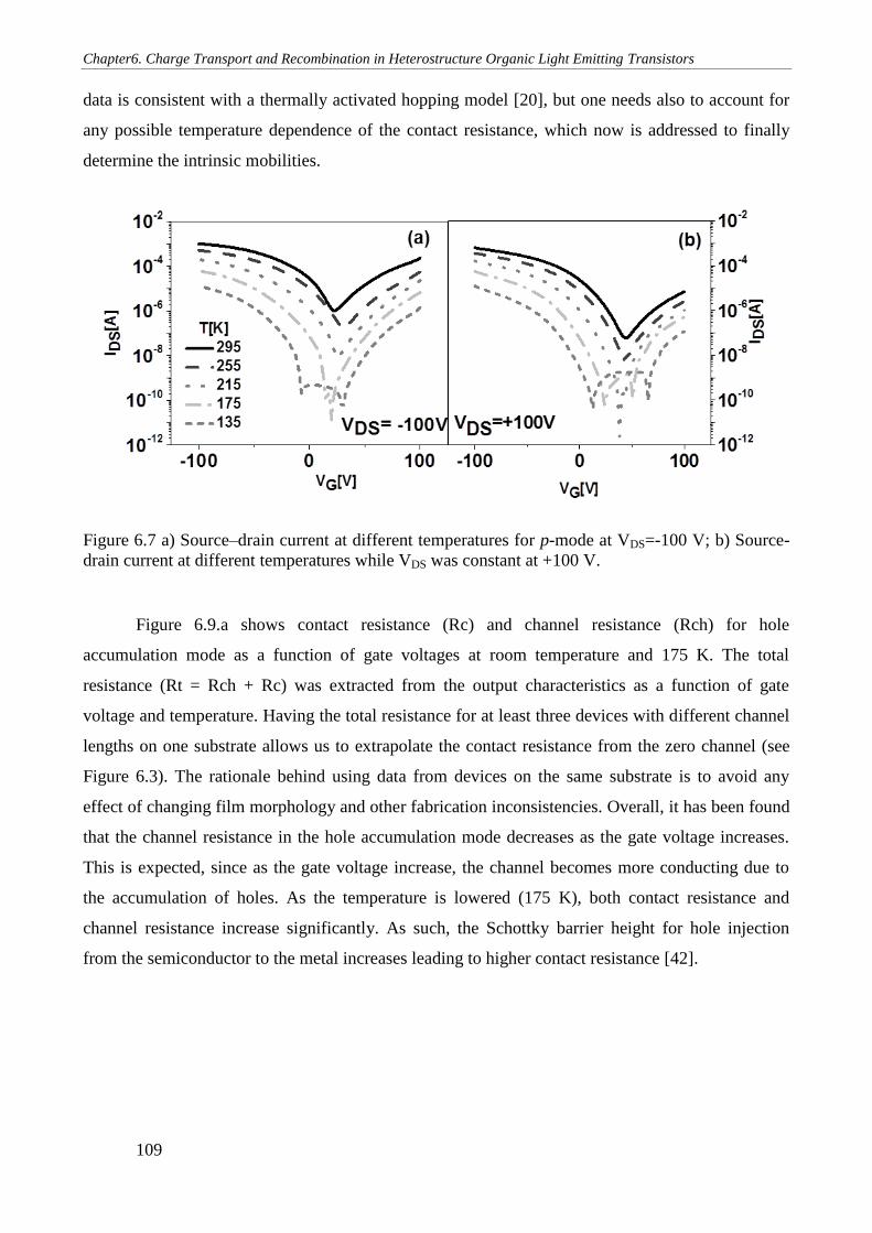
Chapter6. Charge Transport and Recombination in Heterostructure Organic Light Emitting Transistors
109
data is consistent with a thermally activated hopping model [20], but one needs also to account for
any possible temperature dependence of the contact resistance, which now is addressed to finally
determine the intrinsic mobilities.
Figure 6.7 a) Source–drain current at different temperatures for p-mode at VDS=-100 V; b) Source-
drain current at different temperatures while VDS was constant at +100 V.
Figure 6.9.a shows contact resistance (Rc) and channel resistance (Rch) for hole
accumulation mode as a function of gate voltages at room temperature and 175 K. The total
resistance (Rt = Rch + Rc) was extracted from the output characteristics as a function of gate
voltage and temperature. Having the total resistance for at least three devices with different channel
lengths on one substrate allows us to extrapolate the contact resistance from the zero channel (see
Figure 6.3). The rationale behind using data from devices on the same substrate is to avoid any
effect of changing film morphology and other fabrication inconsistencies. Overall, it has been found
that the channel resistance in the hole accumulation mode decreases as the gate voltage increases.
This is expected, since as the gate voltage increase, the channel becomes more conducting due to
the accumulation of holes. As the temperature is lowered (175 K), both contact resistance and
channel resistance increase significantly. As such, the Schottky barrier height for hole injection
from the semiconductor to the metal increases leading to higher contact resistance [42].
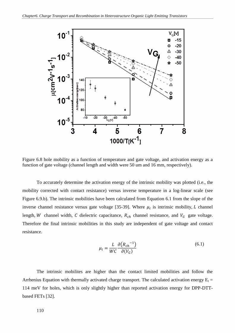
Chapter6. Charge Transport and Recombination in Heterostructure Organic Light Emitting Transistors
110
Figure 6.8 hole mobility as a function of temperature and gate voltage, and activation energy as a
function of gate voltage (channel length and width were 50 um and 16 mm, respectively).
To accurately determine the activation energy of the intrinsic mobility was plotted (i.e., the
mobility corrected with contact resistance) versus inverse temperature in a log-linear scale (see
Figure 6.9.b). The intrinsic mobilities have been calculated from Equation 6.1 from the slope of the
inverse channel resistance versus gate voltage [35-39]. Where 𝜇𝑖 is intrinsic mobility, 𝐿 channel
length, 𝑊 channel width, 𝐶 dielectric capacitance, 𝑅𝑐ℎ channel resistance, and 𝑉𝐺 gate voltage.
Therefore the final intrinsic mobilities in this study are independent of gate voltage and contact
resistance.
𝜇𝑖 =
𝐿
𝑊𝐶
𝜕(𝑅𝑐ℎ−1)
𝜕(𝑉𝐺)
(6.1)
The intrinsic mobilites are higher than the contact limited mobilities and follow the
Arrhenius Equation with thermally activated charge transport. The calculated activation energy Et =
114 meV for holes, which is only slightly higher than reported activation energy for DPP-DTT-
based FETs [32].
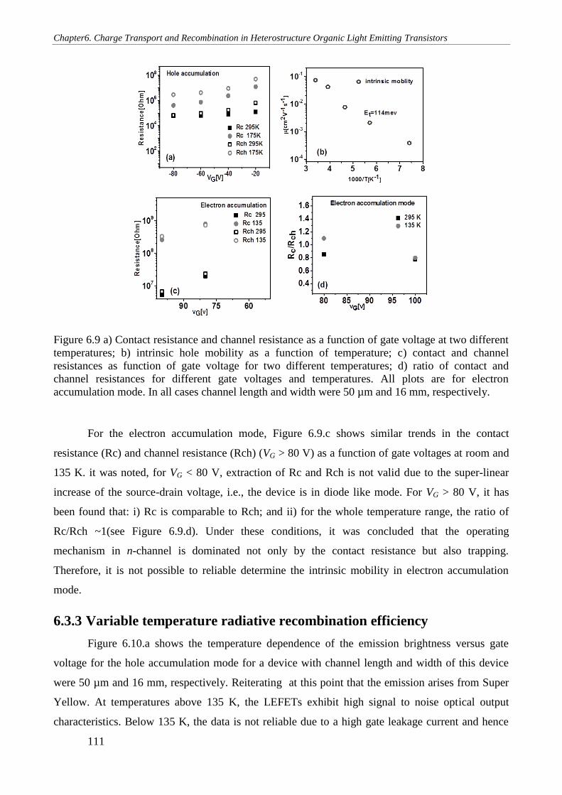
Chapter6. Charge Transport and Recombination in Heterostructure Organic Light Emitting Transistors
111
Figure 6.9 a) Contact resistance and channel resistance as a function of gate voltage at two different
temperatures; b) intrinsic hole mobility as a function of temperature; c) contact and channel
resistances as function of gate voltage for two different temperatures; d) ratio of contact and
channel resistances for different gate voltages and temperatures. All plots are for electron
accumulation mode. In all cases channel length and width were 50 µm and 16 mm, respectively.
For the electron accumulation mode, Figure 6.9.c shows similar trends in the contact
resistance (Rc) and channel resistance (Rch) (VG > 80 V) as a function of gate voltages at room and
135 K. it was noted, for VG < 80 V, extraction of Rc and Rch is not valid due to the super-linear
increase of the source-drain voltage, i.e., the device is in diode like mode. For VG > 80 V, it has
been found that: i) Rc is comparable to Rch; and ii) for the whole temperature range, the ratio of
Rc/Rch ~1(see Figure 6.9.d). Under these conditions, it was concluded that the operating
mechanism in n-channel is dominated not only by the contact resistance but also trapping.
Therefore, it is not possible to reliable determine the intrinsic mobility in electron accumulation
mode.
6.3.3 Variable temperature radiative recombination efficiency
Figure 6.10.a shows the temperature dependence of the emission brightness versus gate
voltage for the hole accumulation mode for a device with channel length and width of this device
were 50 µm and 16 mm, respectively. Reiterating at this point that the emission arises from Super
Yellow. At temperatures above 135 K, the LEFETs exhibit high signal to noise optical output
characteristics. Below 135 K, the data is not reliable due to a high gate leakage current and hence
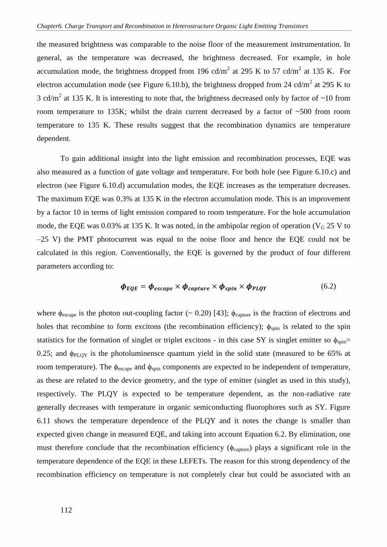
Chapter6. Charge Transport and Recombination in Heterostructure Organic Light Emitting Transistors
112
the measured brightness was comparable to the noise floor of the measurement instrumentation. In
general, as the temperature was decreased, the brightness decreased. For example, in hole
accumulation mode, the brightness dropped from 196 cd/m2 at 295 K to 57 cd/m
2 at 135 K. For
electron accumulation mode (see Figure 6.10.b), the brightness dropped from 24 cd/m2 at 295 K to
3 cd/m2 at 135 K. It is interesting to note that, the brightness decreased only by factor of ~10 from
room temperature to 135K; whilst the drain current decreased by a factor of ~500 from room
temperature to 135 K. These results suggest that the recombination dynamics are temperature
dependent.
To gain additional insight into the light emission and recombination processes, EQE was
also measured as a function of gate voltage and temperature. For both hole (see Figure 6.10.c) and
electron (see Figure 6.10.d) accumulation modes, the EQE increases as the temperature decreases.
The maximum EQE was 0.3% at 135 K in the electron accumulation mode. This is an improvement
by a factor 10 in terms of light emission compared to room temperature. For the hole accumulation
mode, the EQE was 0.03% at 135 K. It was noted, in the ambipolar region of operation (VG 25 V to
–25 V) the PMT photocurrent was equal to the noise floor and hence the EQE could not be
calculated in this region. Conventionally, the EQE is governed by the product of four different
parameters according to:
𝝓𝑬𝑸𝑬 = 𝝓𝒆𝒔𝒄𝒂𝒑𝒆 × 𝝓𝒄𝒂𝒑𝒕𝒖𝒓𝒆 × 𝝓𝒔𝒑𝒊𝒏 × 𝝓𝑷𝑳𝑸𝒀 (6.2)
where ϕescape is the photon out-coupling factor (~ 0.20) [43]; ϕcapture is the fraction of electrons and
holes that recombine to form excitons (the recombination efficiency); ϕspin is related to the spin
statistics for the formation of singlet or triplet excitons - in this case SY is singlet emitter so ϕspin=
0.25; and ϕPLQY is the photoluminensce quantum yield in the solid state (measured to be 65% at
room temperature). The ϕescape and ϕspin components are expected to be independent of temperature,
as these are related to the device geometry, and the type of emitter (singlet as used in this study),
respectively. The PLQY is expected to be temperature dependent, as the non-radiative rate
generally decreases with temperature in organic semiconducting fluorophores such as SY. Figure
6.11 shows the temperature dependence of the PLQY and it notes the change is smaller than
expected given change in measured EQE, and taking into account Equation 6.2. By elimination, one
must therefore conclude that the recombination efficiency (ϕcapture) plays a significant role in the
temperature dependence of the EQE in these LEFETs. The reason for this strong dependency of the
recombination efficiency on temperature is not completely clear but could be associated with an
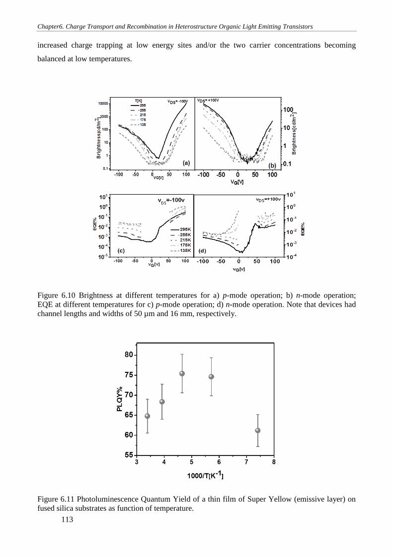
Chapter6. Charge Transport and Recombination in Heterostructure Organic Light Emitting Transistors
113
increased charge trapping at low energy sites and/or the two carrier concentrations becoming
balanced at low temperatures.
Figure 6.10 Brightness at different temperatures for a) p-mode operation; b) n-mode operation;
EQE at different temperatures for c) p-mode operation; d) n-mode operation. Note that devices had
channel lengths and widths of 50 µm and 16 mm, respectively.
Figure 6.11 Photoluminescence Quantum Yield of a thin film of Super Yellow (emissive layer) on
fused silica substrates as function of temperature.
Chapter6. Charge Transport and Recombination in Heterostructure Organic Light Emitting Transistors
114
6.4 Conclusion
In summary, charge transport (mobility and charge injection) and emissive (radiative
recombination, brightness, EQE) properties of organic semiconducting polymers were measured in
a heterostructure light-emitting field effect transistor. Our results demonstrate that, as the LEFET
was cooled down, the intrinsic hole mobilities follow an Arrhenius response with activation energy
of Et = 114 meV and the overall EQE increases. While the PLQY of the emissive polymer increases
with decreasing temperature it is insufficient to explain the improved EQE. Therefore, the improved
EQE at low temperature is primarily due to an increased radiative recombination. Our results
establish some basic rules for engineering high radiative efficiencies in light-emitting field effect
transistors, which should aid in both materials and architecture design.
Chapter6. Charge Transport and Recombination in Heterostructure Organic Light Emitting Transistors
115
References
[1] A.J. Heeger, N.S. Sariciftci, E.B. Namdas, Semiconducting and metallic polymers, Oxford
University Press, 2010.
[2] M. Muccini, A bright future for organic field-effect transistors, Nature materials, 5 (2006) 605-
613.
[3] M. McCarthy, B. Liu, E. Donoghue, I. Kravchenko, D. Kim, F. So, A. Rinzler, Low-voltage,
low-power, organic light-emitting transistors for active matrix displays, Science, 332 (2011) 570-
573.
[4] M. Ahles, A. Hepp, R. Schmechel, H. von Seggern, Light emission from a polymer transistor,
Applied physics letters, 84 (2004) 428-430.
[5] E.B. Namdas, J.S. Swensen, P. Ledochowitsch, J.D. Yuen, D. Moses, A.J. Heeger, Gate‐Controlled Light Emitting Diodes, Advanced Materials, 20 (2008) 1321-1324.
[6] E.B. Namdas, P. Ledochowitsch, J.D. Yuen, D. Moses, A.J. Heeger, High performance light
emitting transistors, Applied Physics Letters, 92 (2008) 183304.
[7] A. Hepp, H. Heil, W. Weise, M. Ahles, R. Schmechel, H. von Seggern, Light-emitting field-
effect transistor based on a tetracene thin film, Physical review letters, 91 (2003) 157406.
[8] J. Veres, S. Ogier, G. Lloyd, D. De Leeuw, Gate insulators in organic field-effect transistors,
Chemistry of Materials, 16 (2004) 4543-4555.
[9] R. Naber, M. Bird, H. Sirringhaus, A gate dielectric that enables high ambipolar mobilities in
polymer light-emitting field-effect transistors, Applied Physics Letters, 93 (2008) 023301.
[10] B.B. Hsu, J. Seifter, C.J. Takacs, C. Zhong, H.-R. Tseng, I.D. Samuel, E.B. Namdas, G.C.
Bazan, F. Huang, Y. Cao, Ordered polymer nanofibers enhance output brightness in bilayer light-
emitting field-effect transistors, ACS nano, 7 (2013) 2344-2351.
[11] J.H. Seo, E.B. Namdas, A. Gutacker, A.J. Heeger, G.C. Bazan, Conjugated polyelectrolytes for
organic light emitting transistors, Applied Physics Letters, 97 (2010) 043303.
[12] J.H. Seo, E.B. Namdas, A. Gutacker, A.J. Heeger, G.C. Bazan, Solution‐Processed Organic
Light‐Emitting Transistors Incorporating Conjugated Polyelectrolytes, Advanced Functional
Materials, 21 (2011) 3667-3672.
[13] E.B. Namdas, B.B. Hsu, J.D. Yuen, I.D. Samuel, A.J. Heeger, Optoelectronic Gate Dielectrics
for High Brightness and High‐Efficiency Light‐Emitting Transistors, Advanced Materials, 23
(2011) 2353-2356.
[14] B.B. Hsu, C. Duan, E.B. Namdas, A. Gutacker, J.D. Yuen, F. Huang, Y. Cao, G.C. Bazan, I.D.
Samuel, A.J. Heeger, Control of Efficiency, Brightness, and Recombination Zone in Light‐Emitting
Field Effect Transistors, Advanced Materials, 24 (2012) 1171-1175.
[15] M. Ullah, K. Tandy, S.D. Yambem, M. Aljada, P.L. Burn, P. Meredith, E.B. Namdas,
Simultaneous enhancement of brightness, efficiency, and switching in RGB organic light emitting
transistors, Advanced Materials, 25 (2013) 6213-6218.
[16] E.B. Namdas, B.B. Hsu, Z. Liu, S.C. Lo, P.L. Burn, I.D. Samuel, Phosphorescent Light‐Emitting Transistors: Harvesting Triplet Excitons, Advanced Materials, 21 (2009) 4957-4961.
[17] K. Tandy, M. Ullah, P.L. Burn, P. Meredith, E.B. Namdas, Unlocking the full potential of light
emitting field-effect transistors by engineering charge injection layers, Organic Electronics, 14
(2013) 2953-2961.
[18] G. Horowitz, R. Hajlaoui, P. Delannoy, Temperature dependence of the field-effect mobility of
sexithiophene. Determination of the density of traps, Journal de Physique III, 5 (1995) 355-371.
[19] I. Hulea, S. Fratini, H. Xie, C. Mulder, N. Iossad, G. Rastelli, S. Ciuchi, A. Morpurgo, Tunable
Fröhlich polarons in organic single-crystal transistors, Nature Materials, 5 (2006) 982-986.
[20] H. Bässler, Charge transport in disordered organic photoconductors, phys. status solidi b, 175
(1993) 15-56.
[21] N.F. Mott, E.A. Davis, Electronic processes in non-crystalline materials, Oxford University
Press, 2012.
Chapter6. Charge Transport and Recombination in Heterostructure Organic Light Emitting Transistors
116
[22] M. Ullah, PhD dissertation , Johannes Kepler University, Linz (2011).
[23] S. Nelson, Y.-Y. Lin, D. Gundlach, T. Jackson, Temperature-independent transport in high-
mobility pentacene transistors, Applied physics letters, 72 (1998) 1854-1856.
[24] A. Brown, C. Jarrett, D. De Leeuw, M. Matters, Field-effect transistors made from solution-
processed organic semiconductors, Synthetic metals, 88 (1997) 37-55.
[25] G. Juska, K. Arlauskas, R. Österbacka, H. Stubb, Time-of-flight measurements in thin films of
regioregular poly (3-hexyl thiophene), Synthetic metals, 109 (2000) 173-176.
[26] A. Armin, M. Velusamy, P.L. Burn, P. Meredith, A. Pivrikas, Injected charge extraction by
linearly increasing voltage for bimolecular recombination studies in organic solar cells, Applied
Physics Letters, 101 (2012) 083306.
[27] A. Armin, G. Juska, M. Ullah, M. Velusamy, P.L. Burn, P. Meredith, A. Pivrikas, Balanced
Carrier Mobilities: Not a Necessary Condition for High‐Efficiency Thin Organic Solar Cells as
Determined by MIS‐CELIV, Advanced Energy Materials, 4 (2014).
[28] M.N. Islam, B. Mazhari, An analytical model for current crowding and source contact
resistance in top-contact organic thin-film transistors, Semiconductor Science and Technology, 23
(2008) 125027.
[29] M. Shur, T. Fjeldly, T. Ytterdal, K. Lee, Unified MOSFET model, Solid-state electronics, 35
(1992) 1795-1802.
[30] G. Reeves, H. Harrison, Obtaining the specific contact resistance from transmission line model
measurements, Electron Device Letters, IEEE, 3 (1982) 111-113.
[31] A.K. Agarwal, B. Mazhari, Simultaneous extraction of source and drain resistances in top
contact organic thin film transistors from a single test structure, Organic Electronics, 13 (2012)
2659-2666.
[32] J. Li, Y. Zhao, H.S. Tan, Y. Guo, C.-A. Di, G. Yu, Y. Liu, M. Lin, S.H. Lim, Y. Zhou, A stable
solution-processed polymer semiconductor with record high-mobility for printed transistors,
Scientific reports, 2 (2012).
[33] P. Wolfer, A. Armin, A. Pivrikas, M. Velusamy, P.L. Burn, P. Meredith, Solution structure:
defining polymer film morphology and optoelectronic device performance, J. Mater. Chem. C, 2
(2013) 71-77.
[34] N.C. Greenham, R.H. Friend, D.D. Bradley, Angular Dependence of the Emission from a
Conjugated Polymer Light‐Emitting Diode: Implications for efficiency calculations, Advanced
Materials, 6 (1994) 491-494.
[35] T. Van Woudenbergh, P. Blom, M. Vissenberg, J. Huiberts, Temperature dependence of the
charge injection in poly-dialkoxy-p-phenylene vinylene, Applied Physics Letters, 79 (2001) 1697-
1699.
[36] L. Bürgi, T. Richards, R. Friend, H. Sirringhaus, Close look at charge carrier injection in
polymer field-effect transistors, Journal of Applied Physics, 94 (2003) 6129-6137.
[37] H. Klauk, G. Schmid, W. Radlik, W. Weber, L. Zhou, C.D. Sheraw, J.A. Nichols, T.N.
Jackson, Contact resistance in organic thin film transistors, Solid-State Electronics, 47 (2003) 297-
301.
[38] J. Zaumseil, K.W. Baldwin, J.A. Rogers, Contact resistance in organic transistors that use
source and drain electrodes formed by soft contact lamination, Journal of Applied Physics, 93
(2003) 6117-6124.
[39] E. Meijer, G. Gelinck, E. Van Veenendaal, B.-H. Huisman, D. De Leeuw, T. Klapwijk, Scaling
behavior and parasitic series resistance in disordered organic field-effect transistors, Applied
physics letters, 82 (2003) 4576-4578.
[40] N. Greenham, I. Samuel, G. Hayes, R. Phillips, Y. Kessener, S. Moratti, A. Holmes, R. Friend,
Measurement of absolute photoluminescence quantum efficiencies in conjugated polymers,
Chemical physics letters, 241 (1995) 89-96.
Chapter6. Charge Transport and Recombination in Heterostructure Organic Light Emitting Transistors
117
[41] M. Ullah, K. Tandy, J. Li, Z. Shi, P.L. Burn, P. Meredith, E.B. Namdas, High-Mobility,
Heterostructure Light-Emitting Transistors and Complementary Inverters, Acs Photonics, 1 (2014)
954-959.
[42] T.D. Anthopoulos, C. Tanase, S. Setayesh, E.J. Meijer, J.C. Hummelen, P.W. Blom, D.M. de
Leeuw, Ambipolar organic field‐effect transistors based on a solution‐processed methanofullerene,
Advanced Materials, 16 (2004) 2174-2179.
[43] A. Boudrioua, P. Hobson, B. Matterson, I. Samuel, W. Barnes, Birefringence and dispersion of
the light emitting polymer MEH–PPV, Synthetic metals, 111 (2000) 545-547.
118
Chapter 7
Summary, Conclusions, and Outlook
The focus of the work presented in this thesis is divided into two parts. The first focus was
on a new, solution processable dendritic class of OLED materials emitting yellow-green colours
suitable for mass production techniques such as spin coating and inkjet printing. The dendritic
structure was employed to provide independent control over photophysical properties without
negatively impacting on charge transport. Different approaches including altering the type and
number of dendrons and polymerisation of dendrimers were investigated. Throughout the course of
this study, both the photophysical properties and electro-optical performance of these materials in
devices were characterised. The second part of this work was on the basic behaviour of organic
semiconductors including the photophysics and recombination in the LEFET architecture. The
outcome of these studies were towards the dual purpose of having more efficient solution processed
OLEDs for industrial display technology with simpler electrical circuits provided by LEFETs.
In Chapter 1, a summary of the current work and working knowledge of the light emitting
devices which motivated the studies in this thesis was described. This was followed by a summary
of the basic theoretical background applicable to the studies on organic semiconductors, dendritic
structures, photophysical concepts, and temperature dependent measurement methods. The
operational mechanism for standard light emitting devices such as OLEDs and LEFETs were then
discussed. Finally, a summary of the objectives of the study was provided.
The experimental methods, calculations, and materials used throughout the work presented
in this thesis were outlined and explained in Chapter 2. This included diverse discussions from
theoretical and experimental concepts of optical techniques to device fabrication and electrical
characterisation. One of the challenges in this project was the characterisation of dipole orientation
applicable to OLED devices. The dipole orientation had never before been tested at the Centre for
Organic Photonics and Electronics. The angle dependent PL spectrum setup was established and
tested on a reference sample according to prior work in literature.
In Chapter 3, the optical and electrical characterisation of a dendritic material using a
reported iridium complex with biphenyl dendron was described. This work was undertaken as a
reference in order to learn more about the photophysical and device performance of this class of
Chapter7. Summary, Conclusion, and Outlook
119
materials. By introducing the electron transport layer TPBi in neat devices, the electron injection
was enhanced. Further, this induced hole blocking at the recombination zone, providing higher
recombination rates and consequently higher internal quantum efficiencies. The EQE was improved
to 11.5% for neat devices. This result was ten times better than previously reported results (0.1%).
The 23% outcoupling value from this device indicated the possibility of horizontal orientation for
emissive dipoles. This could be justified with the anisotropic orientation of the layer underneath,
which could dominate the orientation of emissive layer.
In Chapter 4, a novel approach was demonstrated for solution-processable phosphorescent
materials by the integration of hole-transporting carbazole-based IrIII dendrimers (D1) into the
polymer backbone to create poly-dendrimer (P1). The maximum EQE values for single layer
dendrimer (D1) and poly(dendrimer) OLEDs were 4.5% and 7% respectively. These results
indicated the advantages of polymerisation on device performance, possibly due to better film
forming and charge balance. The performance of dendrimer D1 in both neat and blended devices
confirmed the outcoupling of 22.5% and 25%, respectively. The most outstanding result was
achieved for poly(dendrimer) with maximum EQE of 30% indicating 40% outcoupling, which
haven’t been reported for solution processed devices before. This is double the theoretical limit of
(20%) requiring additional investigation of dipole orientation. The angular dependent PL
measurements were performed in this regard and revealed the ratio of 73% horizontal dipoles which
is higher than isotropic material with 67%. Moreover, a similar result was found for
poly(dendrimer) P1 which could be due to the heteroleptic structure of these compounds. This is a
new and promising achievement as it allows more efficient OLEDs to be realised via modifications
made to the intrinsic properties of the material.
Further in this chapter, the study was extended using the doubly-dendronised dendrimer
(D2) via adding additional carbazole dendrons to the dendrimer D1. The photophysical properties of
D1 and D2 were characterised as well as their performance in devices. By introducing the second
dendron attached to the ligands of IrIII dendrimers, both the intra- and inter-chain inter-
chromophore interactions could be controlled by core encapsulation, leading to higher PLQY values
in the solid state and longer life times of the emissive species. A drawback of this approach was a
red-shift in the emission colour due to an increase in conjugation length of the ligand. The EQE of
6% was obtained for D2 which is slightly higher than its singly-dendronised counterparts with 4.5%
EQE. This double dendron approach to control optoelectronic properties was also used for
poly(dendrimers), providing the extra advantage of higher solution viscosity.
Chapter7. Summary, Conclusion, and Outlook
120
Although, this family of materials has potential for host-free single layer OLED devices,
blended emissive layers showed further reduction in inter-chromophore interaction and
concentration quenching. Adding a second dendron (i.e., in going from D1 to D2 and P1 to P2)
seems to have an impact on film packing and morphology of the emissive layer, both of which play
a crucial role in influencing device performance.
In Chapter 5, an ambipolar solution processable poly(dendrimer) was described whereby
electron-transporting moieties (oxadiazole) were integrated into a carbazole based poly(dendrimer).
Different distributions of electron and hole moieties were applied in these designs. In spite of the
balance between charge carrier types provided with this approach, the recombination rate could not
be increased sufficiently. The conclusion drawn was that this is likely due to the disorder introduced
into the system with the addition of the electron moieties as well as a decrease in PLQY caused by
quenching.
By using the dual functionality of LEFETs, there is the potential to achieve simultaneous
measurements of the charge transport (mobility and charge injection) and emissive properties
(radiative recombination, brightness, EQE) of organic semiconducting polymers. This was taken
advantage of with the temperature dependent experiments described in Chapter 6. The results
demonstrated that, as the LEFET was cooled down, the intrinsic hole mobilities followed an
Arrhenius response with activation energy of Et = 114 meV, and the overall EQE increased. While
the PLQY of the emissive polymer increased with decreasing temperature it was insufficient to
explain the improved EQE. It was concluded that the improved EQE at low temperatures was
primarily due to an increased radiative recombination. Our results established some basic principles
for engineering high radiative efficiencies in LEFETs, which should aid in both material and
architecture design.
As well as concluding this work and summarising the findings throughout this thesis, it is
necessary to acknowledge the potential next steps generated by these findings as follows:
i) A prospective approach to further increase OLED device performance would be to
make use of an exciplex forming co-host for the emissive materials. In this case,
phosphorescent dendrimers or poly(dendrimers) would be the guest material, and a
combination of electron- and hole transporting materials would be the requirements
for the co-host. This approach can provide the necessary isolation between cores to
prevent concentration quenching, as well as an ambipolar host, which could ease
both charge injection and transport.
Chapter7. Summary, Conclusion, and Outlook
121
ii) A second outlook would be towards more studies on the horizontal orientation of
emissive dipoles. This could significantly enhance the intrinsic properties of the
emissive materials, achieving higher light out-put coupling and hence EQEs without
the need for device modifications. One approach to achieve this is via the creation of
an anisotropic emissive layer provided by the heteroleptic design of emissive
materials, or alternatively an anisotropic host system.
iii) One of the advantages using dendritic structures is the ability to independently
control optical properties of materials while maintaining the electrical properties.
Therefore third outlook suggests altering the emitting color by means of other cores
for red or blue. Giving poly(dendrimers) provided excellent outcoupling and device
performance for green and yellow in the work presented in this thesis, this outlook
can lead to having highly efficient GRB (green-red-blue) pixels in display
technology. A key next step could be studying device stability and degradation
which is crucial for display technology as well as lighting.
iv) Another approach toward highly efficient LEFET devices would be employing the
planar anisotropic materials which simultaneously enhance the charge transport and
direction of light emission. A combination of these ideas could be used in LEFET
structures to provide improved OLED efficiency with switching advantages.
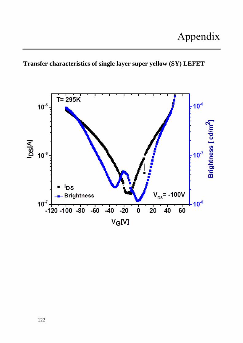
122
Appendix
Transfer characteristics of single layer super yellow (SY) LEFET