near field communication wired interface (nfc-wi)nfc-wi near field communication wired interface ....
TRANSCRIPT
Reference numberECMA-123:2009
© Ecma International 2009
ECMA-373 2nd Edition / June 2012
Near Field Communication Wired Interface (NFC-WI)

COPYRIGHT PROTECTED DOCUMENT
© Ecma International 2012

© Ecma International 2012 i
Contents Page
1 Scope ...................................................................................................................................................... 1
2 Conformance ......................................................................................................................................... 1
3 Normative references ............................................................................................................................ 1
4 Terms and definitions ........................................................................................................................... 1
5 Conventions and notations .................................................................................................................. 1 5.1 Representation of bit values ................................................................................................................ 1 5.2 Representation of logical states of LOW and HIGH ........................................................................... 1 5.3 Capitalisation of names ........................................................................................................................ 2 5.4 State notation ......................................................................................................................................... 2
6 Acronyms ............................................................................................................................................... 2
7 General ................................................................................................................................................... 2 8 Signals .................................................................................................................................................... 3 8.1 Signal wires ............................................................................................................................................ 3 8.1.1 Signal-In ................................................................................................................................................. 3 8.1.2 Signal-Out .............................................................................................................................................. 3 8.2 Electrical characteristics ...................................................................................................................... 3 8.3 Clock frequency (fCLK) ........................................................................................................................... 4 9 NFC-WI states ........................................................................................................................................ 4 9.1 Off state .................................................................................................................................................. 5 9.2 Activating state ...................................................................................................................................... 5 9.2.1 Signal-Out activation ............................................................................................................................. 6 9.2.2 Signal-In activation ................................................................................................................................ 6 9.3 On state .................................................................................................................................................. 7 9.3.1 Idle ........................................................................................................................................................... 8 9.3.2 Busy ........................................................................................................................................................ 8 9.4 De-Activating state ................................................................................................................................ 8 9.4.1 Signal-Out deactivation ........................................................................................................................ 9 9.4.2 Signal-In deactivation ........................................................................................................................... 9 9.5 Command state ...................................................................................................................................... 9 9.5.1 Escape sequence .................................................................................................................................. 9
10 Information-Transfer ........................................................................................................................... 10 10.1 Manchester Bit coding ........................................................................................................................ 10 10.2 Modified Miller Bit coding ................................................................................................................... 10 10.3 Bit coding for fCLK/128 (~106 kb/s) ..................................................................................................... 11 10.3.1 Signal-Out ............................................................................................................................................ 11 10.3.2 Signal-In ............................................................................................................................................... 11 10.4 Bit coding for fCLK/64 (~212 kb/s) ....................................................................................................... 11 10.4.1 Signal-Out ............................................................................................................................................ 11 10.4.2 Signal-In ............................................................................................................................................... 12 10.5 Bit coding for fCLK/32 (~424 kb/s) ....................................................................................................... 12
Annex A (informative) Application of NFC-WI with NFCIP-1 ........................................................................ 13 A.1 General ................................................................................................................................................. 13 A.2 Reference ............................................................................................................................................. 13 A.3 Propagation delay ............................................................................................................................... 13 A.4 Communication Mode ......................................................................................................................... 13 A.5 RF-field control during activation ...................................................................................................... 13 A.5.1 Activation without RF-field ................................................................................................................. 13
ii © Ecma International 2012
A.5.2 Activation with RF-field .......................................................................................................................14 A.6 Signal diagrams ...................................................................................................................................15 A.6.1 fCLK/128 ..................................................................................................................................................15 A.6.2 fCLK/64 ....................................................................................................................................................16 Annex B (informative) Command state ...........................................................................................................17 B.1 Configuration .......................................................................................................................................17
© Ecma International 2012 iii
face
his 2nd edition is fully aligned with the 1st edition of ISO/IEC 28361:2007.
This Ecma Standard has been adopted by the General Assembly of June 2012.
Introduction
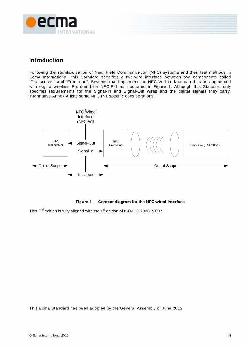
Following the standardisation of Near Field Communication (NFC) systems and their test methods in Ecma International, this Standard specifies a two-wire interface between two components called “Transceiver” and “Front-end”. Systems that implement the NFC-WI interface can thus be augmented with e.g. a wireless Front-end for NFCIP-1 as illustrated in Figure 1. Although this Standard only specifies requirements for the Signal-In and Signal-Out wires and the digital signals they carry, informative Annex A lists some NFCIP-1 specific considerations.
NFCTransceiver Signal-Out
Signal-InDevice (e.g. NFCIP-1)
NFCFront-End
NFC WiredInterface(NFC-WI)
In scope
Out of ScopeOut of Scope
Figure 1 — Context diagram for the NFC wired inter
T

iv © Ecma International 2012
"COPYRIGHT NOTICE
This document may be copied, published and distributed to others, and certain derivative works of it may be prepared, copied, published, and distributed, in whole or in part, provided that the above copyright notice and this Copyright License and Disclaimer are included on all such copies and derivative works. The only derivative works that are permissible under this Copyright License and Disclaimer are:
(i) works which incorporate all or portion of this document for the purpose of providing commentary or explanation (such as an annotated version of the document),
(ii) works which incorporate all or portion of this document for the purpose of incorporating features that provide accessibility,
(iii) translations of this document into languages other than English and into different formats and
(iv) works by making use of this specification in standard conformant products by implementing (e.g. by copy and paste wholly or partly) the functionality therein.
However, the content of this document itself may not be modified in any way, including by removing the copyright notice or references to Ecma International, except as required to translate it into languages other than English or into a different format.
The official version of an Ecma International document is the English language version on the Ecma International website. In the event of discrepancies between a translated version and the official version, the official version shall govern.
The limited permissions granted above are perpetual and will not be revoked by Ecma International or its successors or assigns.
This document and the information contained herein is provided on an "AS IS" basis and ECMA INTERNATIONAL DISCLAIMS ALL WARRANTIES, EXPRESS OR IMPLIED, INCLUDING BUT NOT LIMITED TO ANY WARRANTY THAT THE USE OF THE INFORMATION HEREIN WILL NOT INFRINGE ANY OWNERSHIP RIGHTS OR ANY IMPLIED WARRANTIES OF MERCHANTABILITY OR FITNESS FOR A PARTICULAR PURPOSE."
© Ecma International 2012 1
Near Field Communication Wired Interface (NFC-WI)
1 Scope
This Standard specifies the digital wire interface between a Transceiver and a Front-end. The specification includes the signal wires, binary signals, the state diagrams and the bit encodings for three data rates.
2 Conformance
Conformant Transceivers and Front-ends implement the wired interface specified herein.
3 Normative references
None.
4 Terms and definitions
For the purposes of this document, the following terms and definitions apply.
4.1 Clock sequence of LOW and HIGH as defined in 5.2 with duration of 1/(2*fCLK), where fCLK is the clock frequency as defined in 8.3
4.2 Information Bit-coded data as defined in Clause 10
4.3 Front-end entity that drives the Signal-Out wire and receives on the Signal-In wire
4.4 Transceiver entity that drives the Signal-In wire and receives on the Signal-Out wire
5 Conventions and notations
5.1 Representation of bit values
Bit values are either ZERO or ONE.
5.2 Representation of logical states of LOW and HIGH
⎯ The logical signal state is LOW if the electrical level of a signal has the input voltage of VIL or the output voltage of VOL as specified in Table 1 in 8.2.
2 © Ecma International 2012
⎯ The logical signal state is HIGH if the electrical level of a signal has the input voltage of VIH or the output voltage of VOH as specified in Table 1 in 8.2.
5.3 Capitalisation of names
The initial character of names of basic elements, e.g. specific fields, is capitalised.
5.4 State notation
The states are specified in Unified Modelling Language (UML) notation.
6 Acronyms AND Logical AND operation
fCLK Clock frequency as defined in 8.3
NFC-WI Near Field Communication Wired Interface
OR Logical OR operation
XOR Logical XOR operation
÷ Divide a clock frequency by a constant value.
Table 1 in 8.2 lists additional symbols for electrical characteristics.
7 General
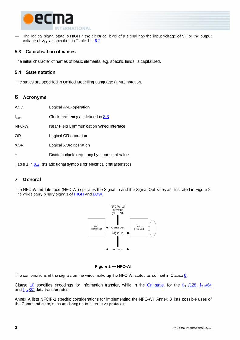
The NFC-Wired Interface (NFC-WI) specifies the Signal-In and the Signal-Out wires as illustrated in Figure 2. The wires carry binary signals of HIGH and LOW.
NFCTransceiver Signal-Out
Signal-In
NFCFront-End
NFC WiredInterface(NFC-WI)
In scope
Figure 2 — NFC-WI
The combinations of the signals on the wires make up the NFC-WI states as defined in Clause 9.
Clause 10 specifies encodings for Information transfer, while in the On state, for the fCLK/128, fCLK/64 and fCLK/32 data transfer rates.
Annex A lists NFCIP-1 specific considerations for implementing the NFC-WI; Annex B lists possible uses of the Command state, such as changing to alternative protocols.
© Ecma International 2012 3
8 Signals
8.1 Signal wires
8.1.1 Signal-In
The Transceiver drives the Signal-In wire with a binary signal of HIGH and LOW. The Front-end receives the binary signal on Signal-In.
8.1.2 Signal-Out
The Front-end drives the Signal-Out wire with a binary signal of HIGH and LOW. The Transceiver receives the binary signal on Signal-Out.
8.2 Electrical characteristics
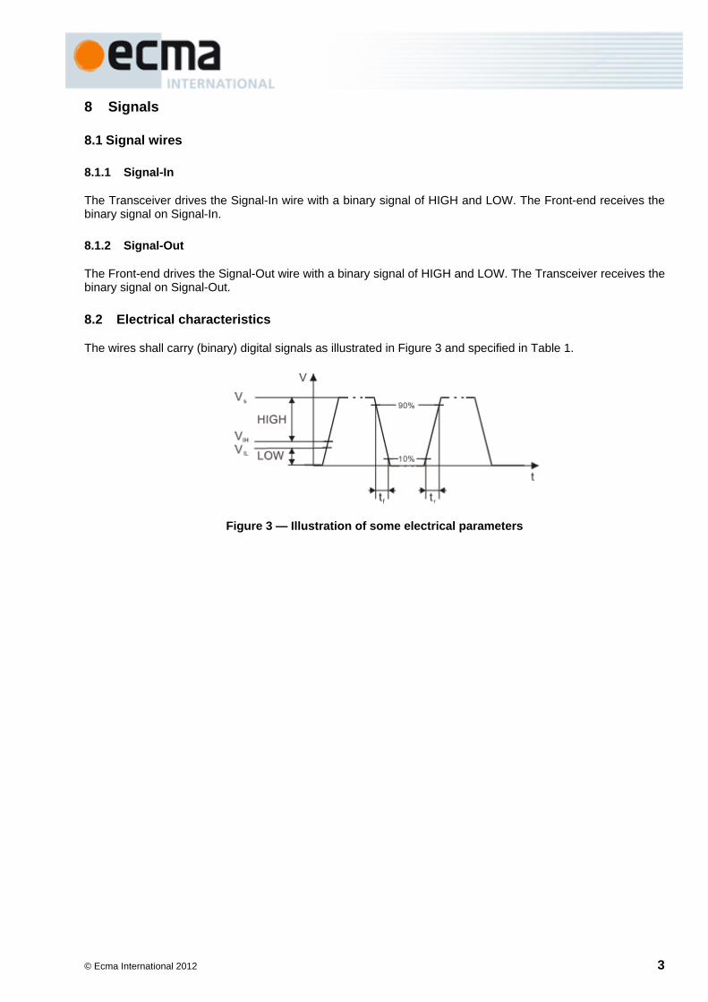
The wires shall carry (binary) digital signals as illustrated in Figure 3 and specified in Table 1.
Figure 3 — Illustration of some electrical parameters
4 © Ecma International 2012
Table 1 — Electrical characteristics
Symbol Parameter Conditions Min Max Unit
DC Characteristics
VS Signalling voltage amplitude Not applicable 1,62 3,63 V
VIH HIGH level input voltage Not applicable 1,10 3,63 V
VIL LOW level input voltage Not applicable 0 0,70 V
ILI Input leakage current Input voltage is between VILmin and VIHmax
± 4 mA
VOH HIGH level output voltage Driver source current of 4mA 1,32 3,63 V
VOL LOW level output voltage Driver sink current of 4mA 0 0,30 V
AC Characteristics
tr Signal-In, Signal-Out rise time (from 10 % to 90 % of VS)
Add an external capacitive load between 10 pF and 30 pF for testing 4 20 ns
tf Signal-In, Signal-Out fall time (from 90 % to 10 % of VS)
Add an external capacitive load between 10 pF and 30 pF for testing 4 20 ns
tSP Pulse width of spikes and glitches which must be suppressed by the input filter
Not applicable 1 ns
CI Input capacitance 1 MHz test frequency 10 pF
CL External load capacitance for the driver Not applicable 30 pF
VITR Input voltage range at signal transitions Not applicable – 0,30 3,93 V
Pulse width Not applicable 30 ns
Environmental / Test Conditions
Tamb Ambient temperature for electrical characteristics measurements Not applicable 20 26 °C
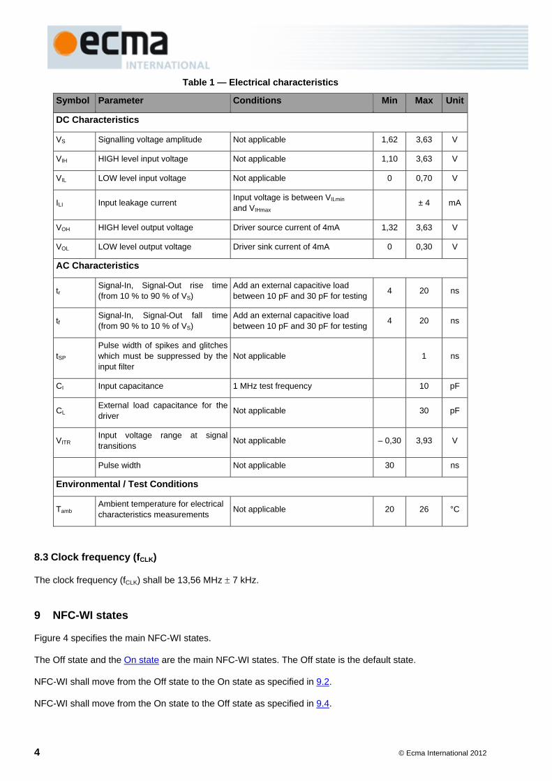
8.3 Clock frequency (fCLK)
The clock frequency (fCLK) shall be 13,56 MHz ± 7 kHz.
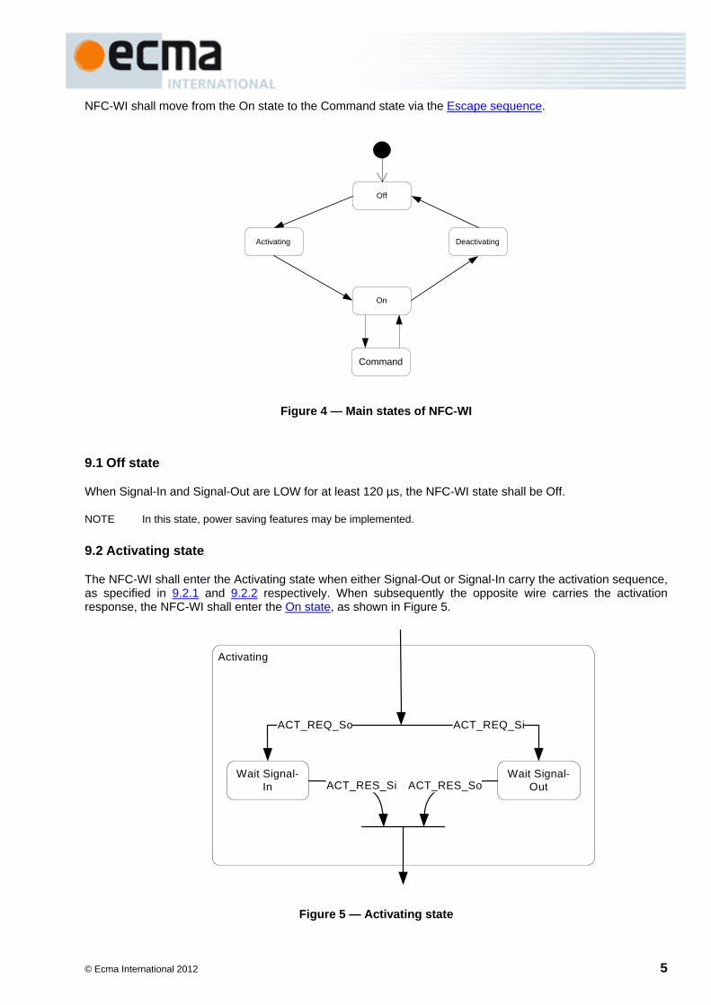
9 NFC-WI states
Figure 4 specifies the main NFC-WI states.
The Off state and the On state are the main NFC-WI states. The Off state is the default state.
NFC-WI shall move from the Off state to the On state as specified in 9.2.
NFC-WI shall move from the On state to the Off state as specified in 9.4.
© Ecma International 2012 5
NFC-WI shall move from the On state to the Command state via the Escape sequence.
Off
On
Activating Deactivating
Command
Figure 4 — Main states of NFC-WI
9.1 Off state
When Signal-In and Signal-Out are LOW for at least 120 µs, the NFC-WI state shall be Off.
NOTE In this state, power saving features may be implemented.
9.2 Activating state
The NFC-WI shall enter the Activating state when either Signal-Out or Signal-In carry the activation sequence, as specified in 9.2.1 and 9.2.2 respectively. When subsequently the opposite wire carries the activation response, the NFC-WI shall enter the On state, as shown in Figure 5.
Activating
Wait Signal-In
Wait Signal-Out
ACT_REQ_So ACT_REQ_Si
ACT_RES_SoACT_RES_Si
Figure 5 — Activating state
6 © Ecma International 2012
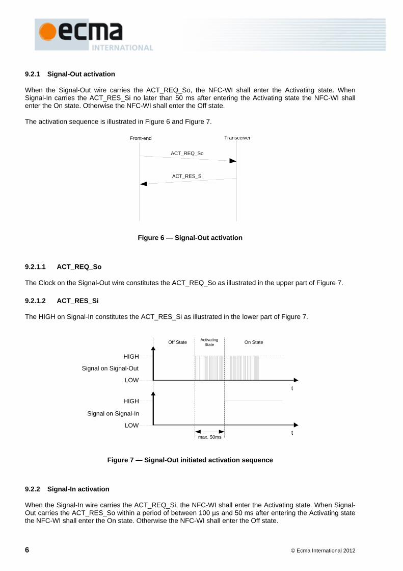
9.2.1 Signal-Out activation
When the Signal-Out wire carries the ACT_REQ_So, the NFC-WI shall enter the Activating state. When Signal-In carries the ACT_RES_Si no later than 50 ms after entering the Activating state the NFC-WI shall enter the On state. Otherwise the NFC-WI shall enter the Off state.
The activation sequence is illustrated in Figure 6 and Figure 7.
TransceiverFront-end
ACT_REQ_So
ACT_RES_Si
Figure 6 — Signal-Out activation
9.2.1.1 ACT_REQ_So
The Clock on the Signal-Out wire constitutes the ACT_REQ_So as illustrated in the upper part of Figure 7.
9.2.1.2 ACT_RES_Si
The HIGH on Signal-In constitutes the ACT_RES_Si as illustrated in the lower part of Figure 7.
HIGH
LOW
Signal on Signal-In
t
HIGH
LOW
Signal on Signal-Out
Off State
t
On StateActivatingState
max. 50ms
Figure 7 — Signal-Out initiated activation sequence
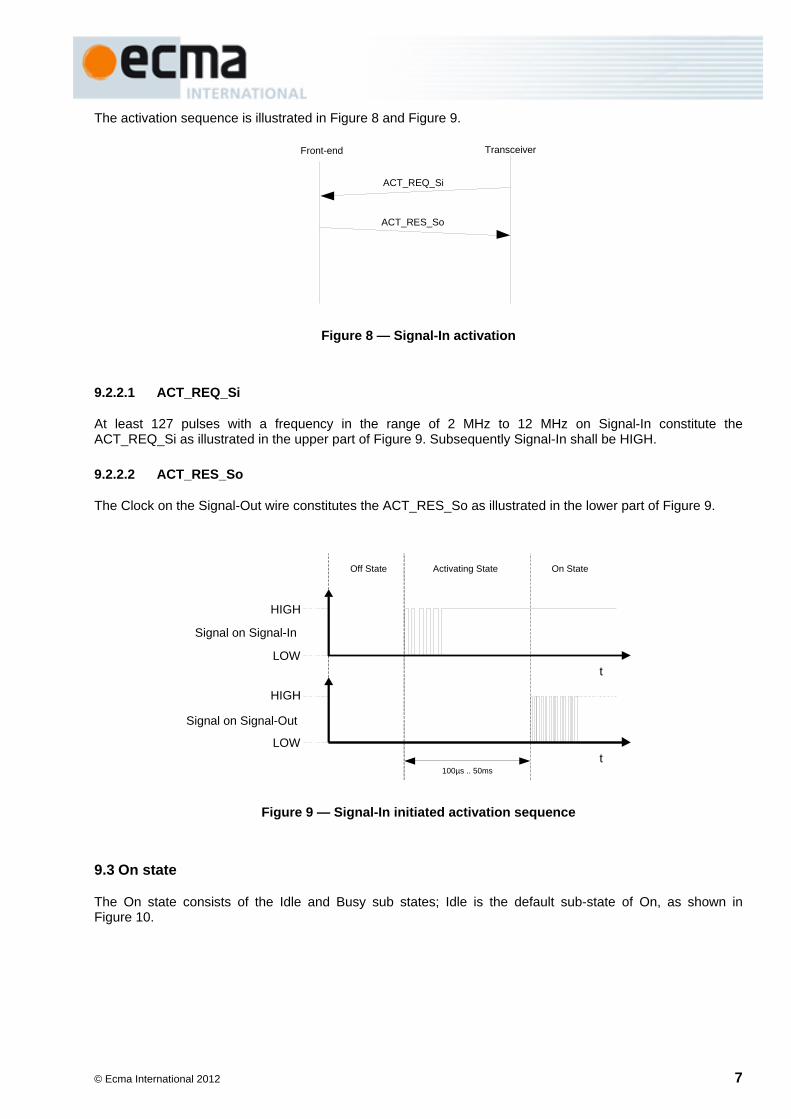
9.2.2 Signal-In activation
When the Signal-In wire carries the ACT_REQ_Si, the NFC-WI shall enter the Activating state. When Signal-Out carries the ACT_RES_So within a period of between 100 µs and 50 ms after entering the Activating state the NFC-WI shall enter the On state. Otherwise the NFC-WI shall enter the Off state.
© Ecma International 2012 7
The activation sequence is illustrated in Figure 8 and Figure 9.
TransceiverFront-end
ACT_REQ_Si
ACT_RES_So
Figure 8 — Signal-In activation
9.2.2.1 ACT_REQ_Si
At least 127 pulses with a frequency in the range of 2 MHz to 12 MHz on Signal-In constitute the ACT_REQ_Si as illustrated in the upper part of Figure 9. Subsequently Signal-In shall be HIGH.
9.2.2.2 ACT_RES_So
The Clock on the Signal-Out wire constitutes the ACT_RES_So as illustrated in the lower part of Figure 9.
HIGH
LOW
Signal on Signal-In
Off State
t
On State
HIGH
LOW
Signal on Signal-Out
t
Activating State
100µs .. 50ms
Figure 9 — Signal-In initiated activation sequence
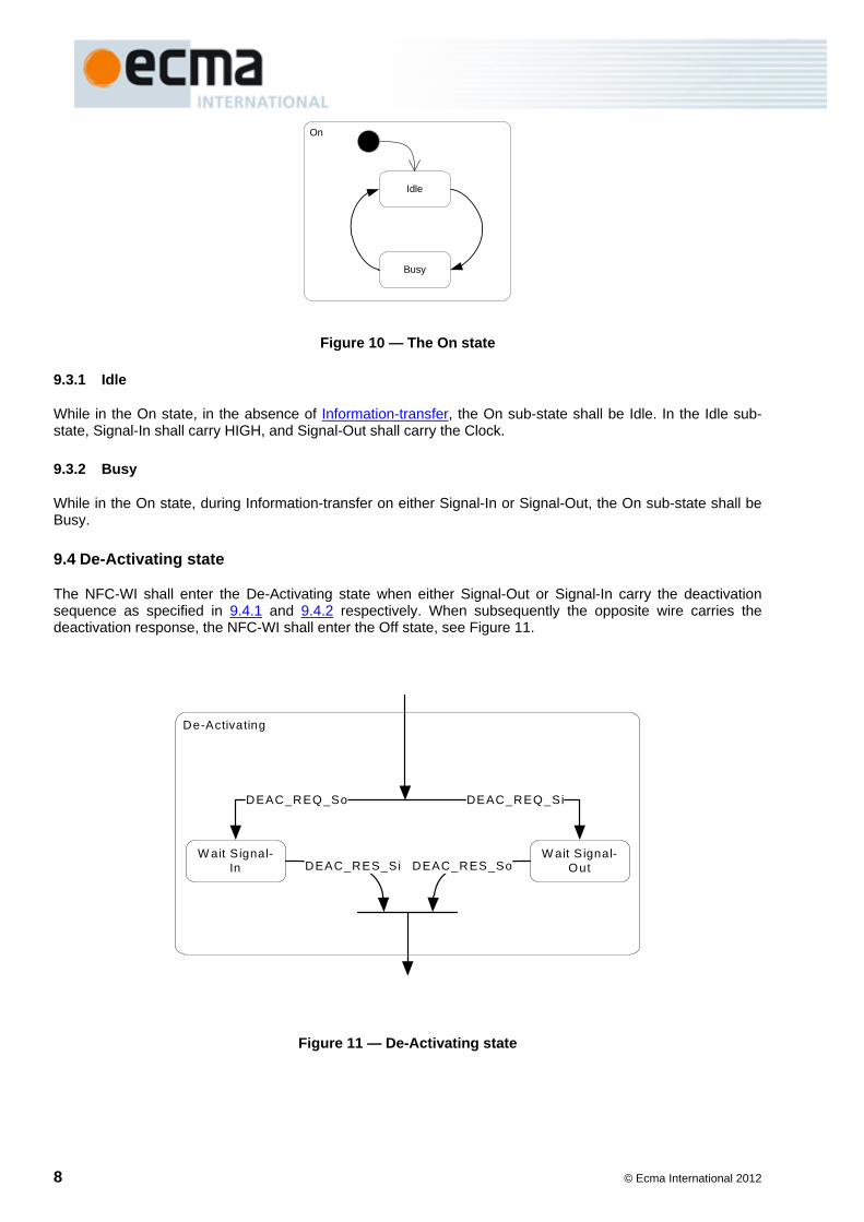
9.3 On state
The On state consists of the Idle and Busy sub states; Idle is the default sub-state of On, as shown in Figure 10.
8 © Ecma International 2012
On
Idle
Busy
Figure 10 — The On state
9.3.1 Idle
While in the On state, in the absence of Information-transfer, the On sub-state shall be Idle. In the Idle sub-state, Signal-In shall carry HIGH, and Signal-Out shall carry the Clock.
9.3.2 Busy
While in the On state, during Information-transfer on either Signal-In or Signal-Out, the On sub-state shall be Busy.
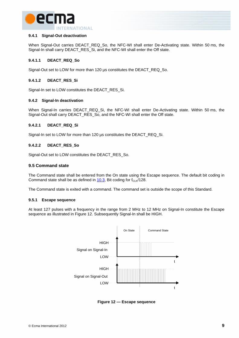
9.4 De-Activating state
The NFC-WI shall enter the De-Activating state when either Signal-Out or Signal-In carry the deactivation sequence as specified in 9.4.1 and 9.4.2 respectively. When subsequently the opposite wire carries the deactivation response, the NFC-WI shall enter the Off state, see Figure 11.
De-Activating
W ait S ignal-In
W ait S ignal-Out
DEAC_REQ_So DEAC_REQ_Si
DEAC_RES_SoDEAC_RES_Si
Figure 11 — De-Activating state
© Ecma International 2012 9
9.4.1 Signal-Out deactivation
When Signal-Out carries DEACT_REQ_So, the NFC-WI shall enter De-Activating state. Within 50 ms, the Signal-In shall carry DEACT_RES_Si, and the NFC-WI shall enter the Off state.
9.4.1.1 DEACT_REQ_So
Signal-Out set to LOW for more than 120 µs constitutes the DEACT_REQ_So.
9.4.1.2 DEACT_RES_Si
Signal-In set to LOW constitutes the DEACT_RES_Si.
9.4.2 Signal-In deactivation
When Signal-In carries DEACT_REQ_Si, the NFC-WI shall enter De-Activating state. Within 50 ms, the Signal-Out shall carry DEACT_RES_So, and the NFC-WI shall enter the Off state.
9.4.2.1 DEACT_REQ_Si
Signal-In set to LOW for more than 120 µs constitutes the DEACT_REQ_Si.
9.4.2.2 DEACT_RES_So
Signal-Out set to LOW constitutes the DEACT_RES_So.
9.5 Command state
The Command state shall be entered from the On state using the Escape sequence. The default bit coding in Command state shall be as defined in 10.3, Bit coding for fCLK/128.
The Command state is exited with a command. The command set is outside the scope of this Standard.
9.5.1 Escape sequence
At least 127 pulses with a frequency in the range from 2 MHz to 12 MHz on Signal-In constitute the Escape sequence as illustrated in Figure 12. Subsequently Signal-In shall be HIGH.
HIGH
LOW
Signal on Signal-In
On State
t
HIGH
LOW
Signal on Signal-Out
t
Command State
Figure 12 — Escape sequence
10 © Ecma International 2012
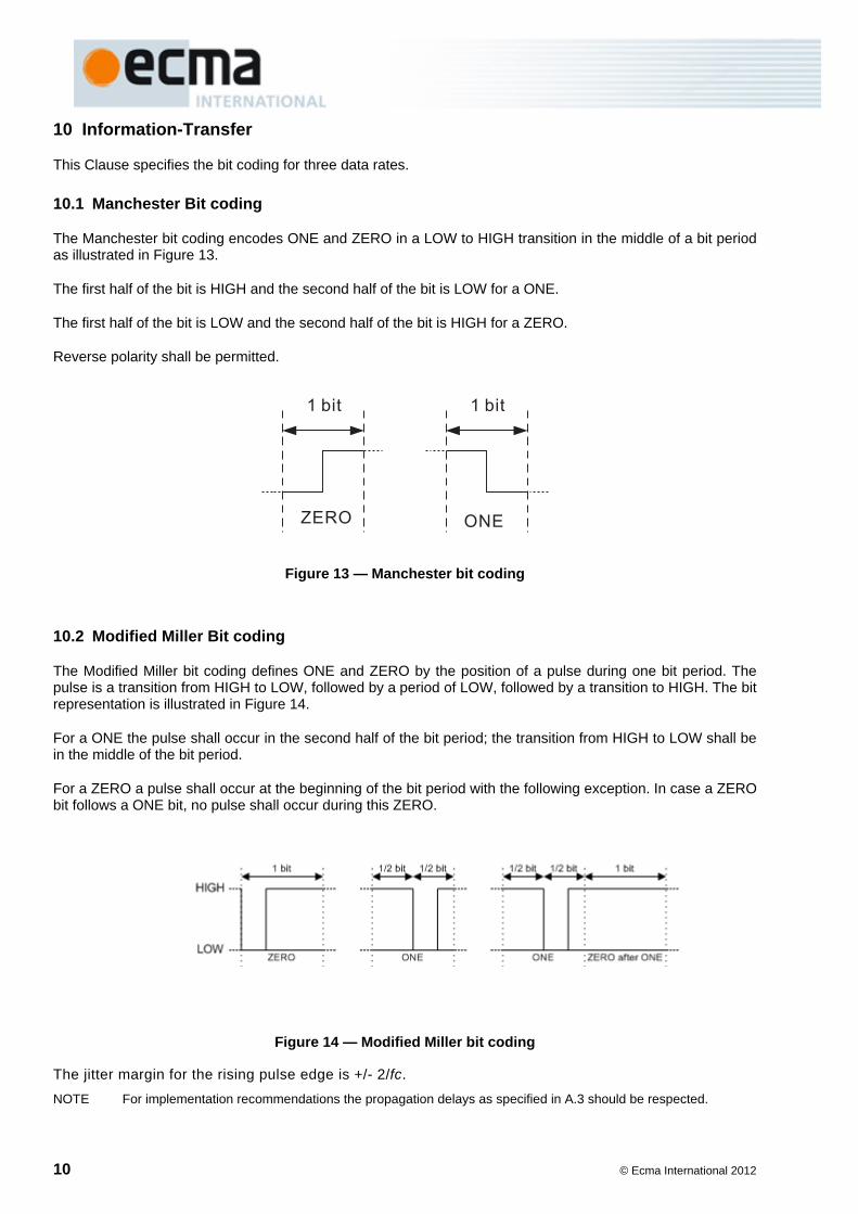
10 Information-Transfer
This Clause specifies the bit coding for three data rates.
10.1 Manchester Bit coding
The Manchester bit coding encodes ONE and ZERO in a LOW to HIGH transition in the middle of a bit period as illustrated in Figure 13.
The first half of the bit is HIGH and the second half of the bit is LOW for a ONE.
The first half of the bit is LOW and the second half of the bit is HIGH for a ZERO.
Reverse polarity shall be permitted.
Figure 13 — Manchester bit coding
10.2 Modified Miller Bit coding
The Modified Miller bit coding defines ONE and ZERO by the position of a pulse during one bit period. The pulse is a transition from HIGH to LOW, followed by a period of LOW, followed by a transition to HIGH. The bit representation is illustrated in Figure 14.
For a ONE the pulse shall occur in the second half of the bit period; the transition from HIGH to LOW shall be in the middle of the bit period.
For a ZERO a pulse shall occur at the beginning of the bit period with the following exception. In case a ZERO bit follows a ONE bit, no pulse shall occur during this ZERO.
Figure 14 — Modified Miller bit coding
The jitter margin for the rising pulse edge is +/- 2/fc.
NOTE For implementation recommendations the propagation delays as specified in A.3 should be respected.
© Ecma International 2012 11
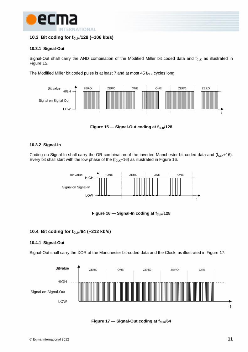
10.3 Bit coding for fCLK/128 (~106 kb/s)
10.3.1 Signal-Out
Signal-Out shall carry the AND combination of the Modified Miller bit coded data and fCLK as illustrated in Figure 15.
The Modified Miller bit coded pulse is at least 7 and at most 45 fCLK cycles long.
LOW
HIGHZERO ZERO ONE ONE ZERO ZERO
Signal on Signal-Out
Bit value
t
Figure 15 — Signal-Out coding at fCLK/128
10.3.2 Signal-In
Coding on Signal-In shall carry the OR combination of the inverted Manchester bit-coded data and (fCLK÷16). Every bit shall start with the low phase of the (fCLK÷16) as illustrated in Figure 16.
LOW
HIGHONE
Signal on Signal-In
Bit value ZERO ONE ONE
t
Figure 16 — Signal-In coding at fCLK/128
10.4 Bit coding for fCLK/64 (~212 kb/s)
10.4.1 Signal-Out
Signal-Out shall carry the XOR of the Manchester bit-coded data and the Clock, as illustrated in Figure 17.
Bitvalue
LOW
HIGH
t
ZERO ONE ZERO ZERO ONE
Signal on Signal-Out
Figure 17 — Signal-Out coding at fCLK/64
12 © Ecma International 2012
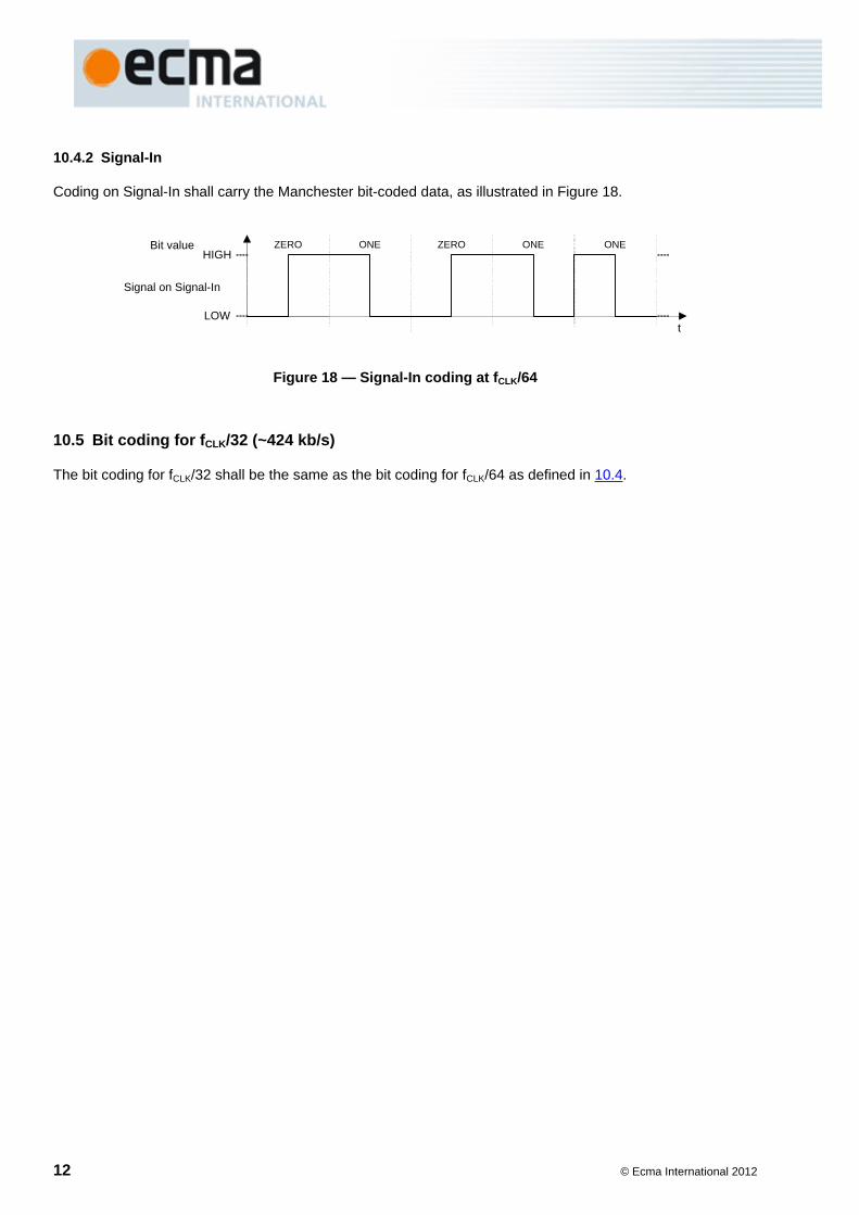
10.4.2 Signal-In
Coding on Signal-In shall carry the Manchester bit-coded data, as illustrated in Figure 18.
LOW
HIGHZERO
Signal on Signal-In
Bit value ONE ZERO ONE
t
ONE
Figure 18 — Signal-In coding at fCLK/64
10.5 Bit coding for fCLK/32 (~424 kb/s)
The bit coding for fCLK/32 shall be the same as the bit coding for fCLK/64 as defined in 10.4.
© Ecma International 2012 13
Annex A (informative)
Application of NFC-WI with NFCIP-1
A.1 General
This Annex lists specific considerations for NFCIP-1 devices that implement NFC-WI.
A.2 Reference
ECMA-340 Near Field Communication - Interface and Protocol (NFCIP-1)
A.3 Propagation delay
The propagation delay of the Front-end is the integer number of clock cycles needed for signal processing in the Front-end. This delay is divided into two parts, one time for Signal-Out (t1) and one for Signal-In (t2). The sum of them is the propagation delay.
ECMA-340 Front-ends, using the NFC-WI interface have the following requirements on the propagation delay:
For data rate fCLK/128: (t1 + t2) equal to 128 clock cycles
For data rate fCLK/64: (t1 + t2) maximum 256 clock cycles
For data rate fCLK/32: (t1 + t2) maximum 256 clock cycles
A.4 Communication Mode
The default communication mode is the Passive communication mode.
A.5 RF-field control during activation
In 9.2, the Standard defines the Activating state.
The activation sequence defined in 9.2.2 only activates the NFC-WI. Whether the NFCIP-1 RF-field is switched on is described by the following two cases.
A.5.1 Activation without RF-field
When ACT_REQ_Si is shorter than 100µs the NFC-WI enters the On state without the Front-end switching on the RF-field.

14 © Ecma International 2012
HIGH
LOW
Signal on Signal-In
Off State
t
On State
HIGH
LOW
Signal on Signal-Out
t
ActivatingState
< 100µs
t
Max
Min
RF-field
Figure A.1 — Activation without RF-field
A.5.2 Activation with RF-field
When ACT_REQ_Si is overlapping the ACT_RES_So for at least 16 clock cycles the NFC-WI enters the On state with the Front-end performing the Initial RF collision avoidance sequence as defined in ECMA-340.
If the Front-end is not able to switch on the RF-field it initiates the Signal-Out deactivation.
HIGH
LOW
Signal on Signal-In
Off State
t
On State
HIGH
LOW
Signal on Signal-Out
t
Activating State
100µs .. 50ms > 16clockcycles
t
Max
Min
RF-field
Figure A.2 — Activation with RF-field
© Ecma International 2012 15
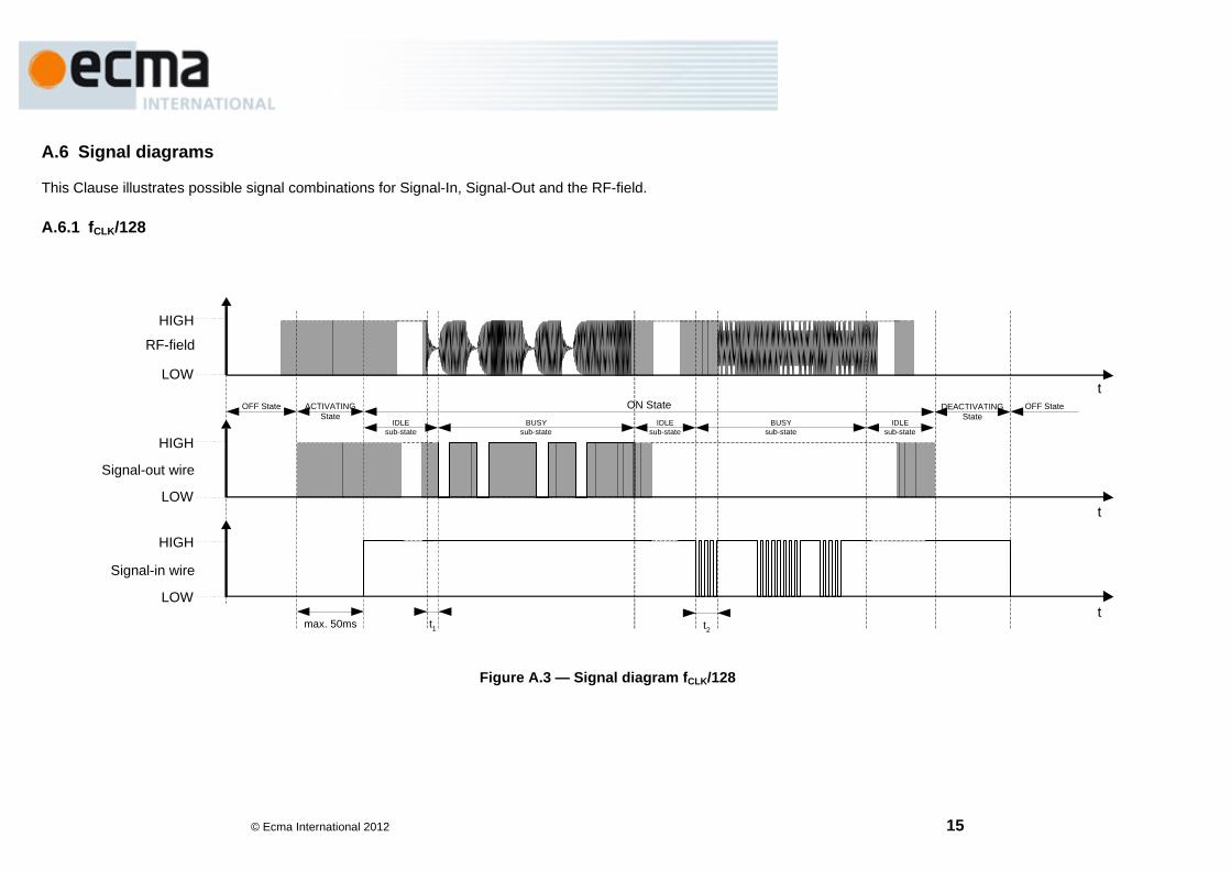
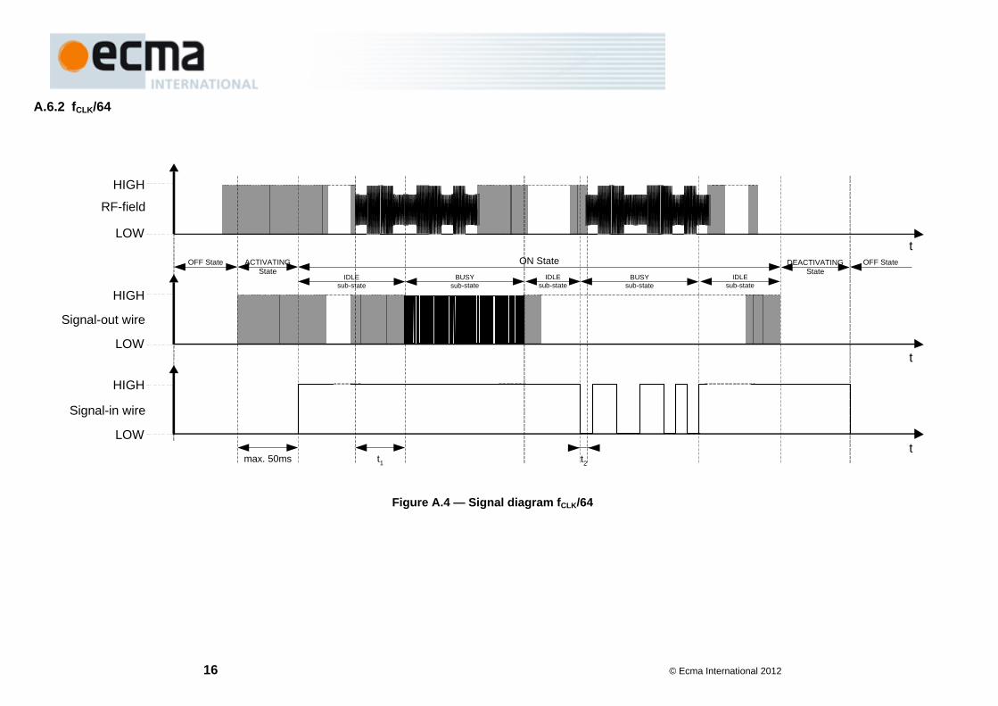
A.6 Signal diagrams
This Clause illustrates possible signal combinations for Signal-In, Signal-Out and the RF-field.
A.6.1 fCLK/128
HIGH
LOW
Signal-in wire
t
HIGH
LOW
Signal-out wire
t
max. 50ms
HIGH
LOW
RF-field
tOFF State ACTIVATING
StateON State
IDLEsub-state
BUSYsub-state
IDLEsub-state
BUSYsub-state
IDLEsub-state
t1 t2
DEACTIVATINGState
OFF State
Figure A.3 — Signal diagram fCLK/128
16 © Ecma International 2012
HIGH
LOW
Signal-in wire
t
HIGH
LOW
Signal-out wire
t
max. 50ms
HIGH
LOW
RF-field
tOFF State ACTIVATING
StateON State
IDLEsub-state
BUSYsub-state
IDLEsub-state
BUSYsub-state
IDLEsub-state
t1 t2
DEACTIVATINGState
OFF State
Figure A.4 — Signal diagram fCLK/64
A.6.2 fCLK/64
Annex B (informative)
Command state
B.1 Configuration
This Standard specifies the Escape sequence to enter the Command state in 9.5. The Command state allows the exchange of control and state information between the Transceiver and the Front-end.
Such exchange may include: indication of the presence of the RF-field; information about the state of the RF-Collision avoidance; control information to change data rates and communication modes. Furthermore, the Command mode allows changing to other communication protocols.
© Ecma International 2012 17

© Ecma International 2012