near electrical resonance signal enhancement...
TRANSCRIPT
http://wrap.warwick.ac.uk
Original citation: Hughes, R., Fan, Yichao and Dixon, Steve. (2014) Near electrical resonance signal enhancement (NERSE) in eddy-current crack detection. NDT & E International, Volume 66 . pp. 82-89. ISSN 0963-8695 Permanent WRAP url: http://wrap.warwick.ac.uk/60500 Copyright and reuse: The Warwick Research Archive Portal (WRAP) makes this work of researchers of the University of Warwick available open access under the following conditions. This article is made available under the Creative Commons Attribution 3.0 (CC BY 3.0) license and may be reused according to the conditions of the license. For more details see: http://creativecommons.org/licenses/by/3.0/ A note on versions: The version presented in WRAP is the published version, or, version of record, and may be cited as it appears here. For more information, please contact the WRAP Team at: [email protected]
Near electrical resonance signal enhancement (NERSE) in eddy-currentcrack detection
R. Hughes a,n, Y. Fan a, S. Dixon a,b
a Department of Physics, University of Warwick, Gibbet Hill Road, Coventry, CV4 7AL, United Kingdomb School of Engineering, University of Warwick, Gibbet Hill Road, Coventry, CV4 7AL, United Kingdom
a r t i c l e i n f o
Article history:Received 5 September 2013Received in revised form23 April 2014Accepted 30 April 2014Available online 9 May 2014
Keywords:Eddy-currentElectrical ResonanceElectromagneticNDTNDECrack Detection
a b s t r a c t
An investigation was performed into the effects of operating an absolute eddy-current testing (ECT)probe at frequencies close to its electrical resonance. A previously undocumented defect signalenhancement phenomenon, resulting from associated shifts in electrical resonant frequency, wasobserved and characterized. Experimental validation was performed on three notch defects on a typicalaerospace superalloy, Titanium 6Al–4V. A conventional absolute ECT probe was operated by sweepingthrough a frequency range about the electrical resonance of the system (1�5 MHz). The phenomenonresults in signal-to-noise ratio (SNR) peak enhancements by a factor of up to 3.7, at frequenciesapproaching resonance, compared to those measured at 1 MHz. The defect signal enhancement peaksare shown to be a result of resonant frequency shifts of the system due to the presence of defects withinthe material. A simple, operational approach for raising the sensitivity of conventional industrial eddy-current testing is proposed, based on the principles of the observed near electrical resonance signalenhancement (NERSE) phenomenon. The simple procedural change of operating within the NERSEfrequency band does not require complex probe design, data analysis or, necessarily, identical coils.Therefore, it is a valuable technique for improving sensitivity, which complements other ECT methods.& 2014 The Authors. Published by Elsevier Ltd. This is an open access article under the CC BY license
(http://creativecommons.org/licenses/by/3.0/).
1. Introduction
Eddy-current testing (ECT) is a well-established non-destruc-tive testing (NDT) technique, routinely implemented in industryfor the inspection of safety-critical metallic components, becauseof its high sensitivity to small surface defects.
High-strength, low density superalloys are used frequently formany industrial applications, particularly in Aerospace [1]. Thedesign and service lifetime of components is based on theassumption that the smallest defect that can be reliably detectedby NDT techniques is present in the part. For this reason, researchis generally focused on detecting smaller defects. Industrial eddy-current methods can reliably detect 0.75 mm long (max 0.38 mmdeep) surface-breaking cracks, but achieving greater sensitivity ishampered by poor signal-to-noise ratios (SNR) [2]. ConventionalECT inspections operate in a range between 100 Hz and 1 MHz [3],so as to avoid the detrimental effects of environmental noise andthe instabilities of electrical resonance. However, superalloystypically have very low electrical conductivities, leading to rela-tively large electromagnetic skin-depths at these frequencies.As a result, conventional operation does not provide sufficient
resolution to the smallest defects, for which higher frequenciesmust be used.
Higher frequency inspections are not without their problems.They suffer from a greater susceptibility to liftoff, and variablesurface conditions due to machining features or conductivitychanges associated with shot-peening or burnishing (common inmany manufacturing processes) [4,5]. This can lead to higherlevels of background noise.
An effective approach for maximizing the SNR of any ECT defectinspection is to use signal averaging, but in an industrial environ-ment this is not always possible or practical, where time andthroughput are important financial considerations. Averaging willalso have a negligible SNR improvement on materials that haverandom but coherent noise (i.e. grain structure). Whilst eddy-current arrays (ECAs) are becoming more commonplace in indus-trial use [6–8] because of their ability to inspect large areas veryquickly, these advantages often come at the cost of resolution andsensitivity. Therefore, it is desirable to develop and implementtechniques that can maximize the sensitivity of single coil andarrayed eddy current probes.
Many authors have implemented multi-frequency, data fusiontechniques [9–11] to cancel out unwanted signals, such as liftoffand temperature variations, so as to improve the SNR. Althoughtechniques such as these have had success in laboratory environ-ments, their application in industry is limited by the longer
Contents lists available at ScienceDirect
journal homepage: www.elsevier.com/locate/ndteint
NDT&E International
http://dx.doi.org/10.1016/j.ndteint.2014.04.0090963-8695/& 2014 The Authors. Published by Elsevier Ltd. This is an open access article under the CC BY license (http://creativecommons.org/licenses/by/3.0/).
n Corresponding author. Tel.: þ44 2476151778.E-mail address: [email protected] (R. Hughes).
NDT&E International 66 (2014) 82–89
inspection times, complex operation and sophisticated signalprocessing algorithms [2,12,13] required. As a result such techni-ques are not commonly used in ECAs.
Authors such as Owston [14], Liu [15,16] and Ko [17,18] haverecognized the potential of measuring the shifting of electricalresonant frequency, due to changes in its environment, as a highlysensitive means of measuring proximity, surface roughness andsurface conductivity variations. The significant power transfer andlarge rates of change around high quality factor resonance peaks inthe electrical impedance of an eddy current coil and cable, offer anextended dynamic range of impedance measurements. Suchadvantages make operating at frequencies around resonancehighly sensitive to even the slightest changes in an electromagne-tically coupled system, but currently there is no documentedaccount of authors exploiting resonance effects specifically fordefect detection.
An investigation was performed on the effects of operating anabsolute ECT probe at frequencies approaching and passing electricalresonance. The research presented in this paper documents theinitial findings of the investigation and highlights the implicationsthat the work will have on future defect inspection techniques.
2. Theory
2.1. Electrical resonance
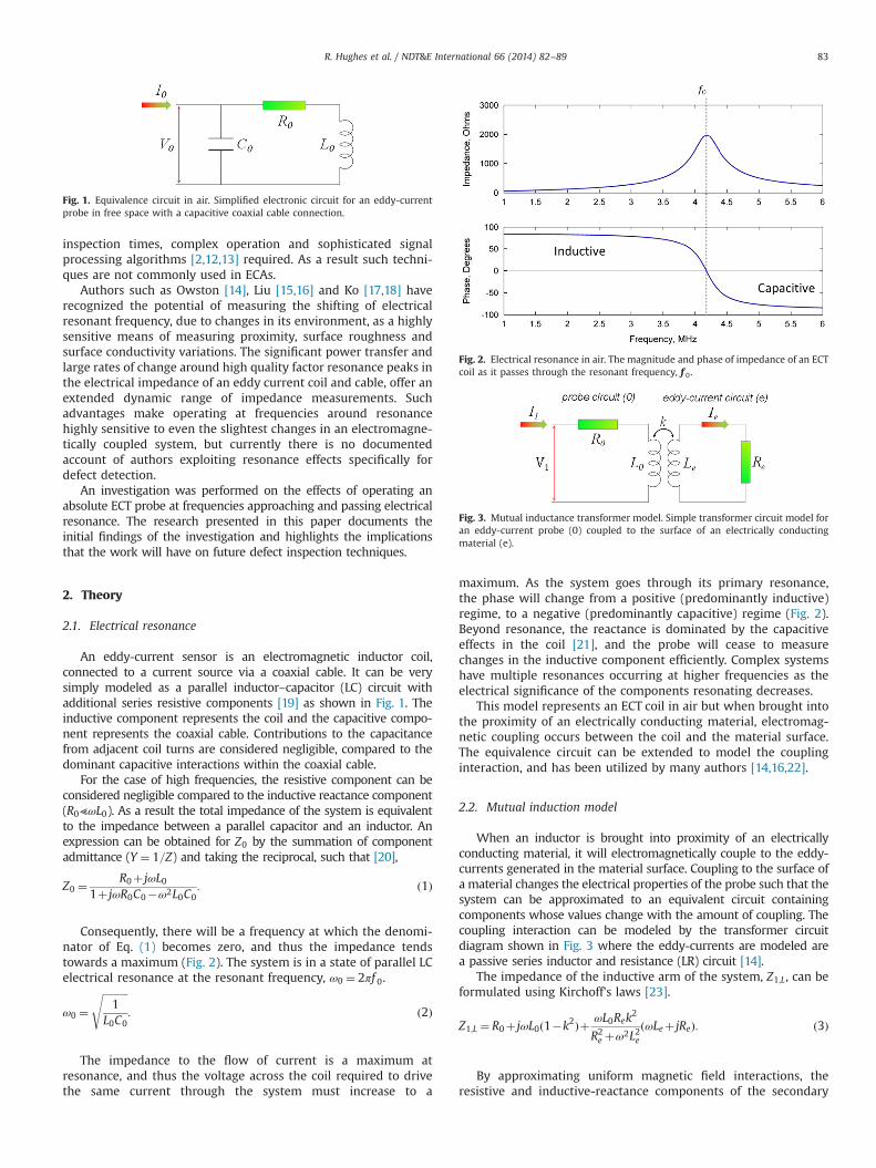
An eddy-current sensor is an electromagnetic inductor coil,connected to a current source via a coaxial cable. It can be verysimply modeled as a parallel inductor–capacitor (LC) circuit withadditional series resistive components [19] as shown in Fig. 1. Theinductive component represents the coil and the capacitive compo-nent represents the coaxial cable. Contributions to the capacitancefrom adjacent coil turns are considered negligible, compared to thedominant capacitive interactions within the coaxial cable.
For the case of high frequencies, the resistive component can beconsidered negligible compared to the inductive reactance component(R0⪡ωL0). As a result the total impedance of the system is equivalentto the impedance between a parallel capacitor and an inductor. Anexpression can be obtained for Z0 by the summation of componentadmittance (Y ¼ 1=Z) and taking the reciprocal, such that [20],
Z0 ¼R0þ jωL0
1þ jωR0C0�ω2L0C0: ð1Þ
Consequently, there will be a frequency at which the denomi-nator of Eq. (1) becomes zero, and thus the impedance tendstowards a maximum (Fig. 2). The system is in a state of parallel LCelectrical resonance at the resonant frequency, ω0 ¼ 2πf 0.
ω0 ¼ffiffiffiffiffiffiffiffiffiffi1
L0C0
s: ð2Þ
The impedance to the flow of current is a maximum atresonance, and thus the voltage across the coil required to drivethe same current through the system must increase to a
maximum. As the system goes through its primary resonance,the phase will change from a positive (predominantly inductive)regime, to a negative (predominantly capacitive) regime (Fig. 2).Beyond resonance, the reactance is dominated by the capacitiveeffects in the coil [21], and the probe will cease to measurechanges in the inductive component efficiently. Complex systemshave multiple resonances occurring at higher frequencies as theelectrical significance of the components resonating decreases.
This model represents an ECT coil in air but when brought intothe proximity of an electrically conducting material, electromag-netic coupling occurs between the coil and the material surface.The equivalence circuit can be extended to model the couplinginteraction, and has been utilized by many authors [14,16,22].
2.2. Mutual induction model
When an inductor is brought into proximity of an electricallyconducting material, it will electromagnetically couple to the eddy-currents generated in the material surface. Coupling to the surface ofa material changes the electrical properties of the probe such that thesystem can be approximated to an equivalent circuit containingcomponents whose values change with the amount of coupling. Thecoupling interaction can be modeled by the transformer circuitdiagram shown in Fig. 3 where the eddy-currents are modeled area passive series inductor and resistance (LR) circuit [14].
The impedance of the inductive arm of the system, Z1;L, can beformulated using Kirchoff's laws [23].
Z1;L ¼ R0þ jωL0ð1�k2Þþ ωL0Rek2
R2e þω2L2e
ðωLeþ jReÞ: ð3Þ
By approximating uniform magnetic field interactions, theresistive and inductive-reactance components of the secondary
Fig. 1. Equivalence circuit in air. Simplified electronic circuit for an eddy-currentprobe in free space with a capacitive coaxial cable connection.
Fig. 2. Electrical resonance in air. The magnitude and phase of impedance of an ECTcoil as it passes through the resonant frequency, f 0.
Fig. 3. Mutual inductance transformer model. Simple transformer circuit model foran eddy-current probe (0) coupled to the surface of an electrically conductingmaterial (e).
R. Hughes et al. / NDT&E International 66 (2014) 82–89 83
circuit are assumed to be equal in magnitude (ωLe ¼ Re) as shownby Wheeler [22]. The impedance of the inductive arm of thecircuit, Z1;L, of the circuit in Fig. 3 therefore reduces to the seriescombination of the probe coil impedance in air, Z0;L, plus addi-tional series resistance and reactance of equal magnitude andfrequency dependence.
Z1;L ¼ R0þ jωL0þ12ωL0k
2ð1� jÞ; ð4Þ
Z1;L ¼ Z0;Lþ12ωL0k
2ð1� jÞ: ð5Þ
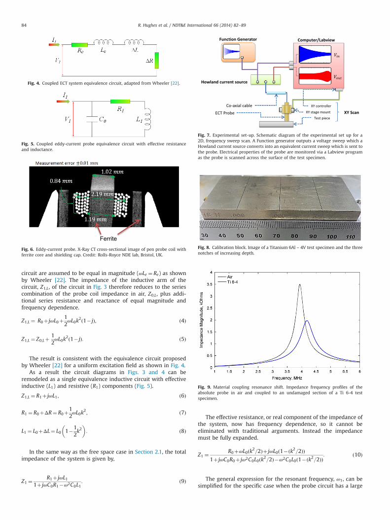
The result is consistent with the equivalence circuit proposedby Wheeler [22] for a uniform excitation field as shown in Fig. 4.
As a result the circuit diagrams in Figs. 3 and 4 can beremodeled as a single equivalence inductive circuit with effectiveinductive (L1) and resistive (R1) components (Fig. 5).
Z1;L ¼ R1þ jωL1; ð6Þ
R1 ¼ R0þΔR¼ R0þ12ωL0k
2; ð7Þ
L1 ¼ L0þΔL¼ L0 1�12k2
� �: ð8Þ
In the same way as the free space case in Section 2.1, the totalimpedance of the system is given by,
Z1 ¼R1þ jωL1
1þ jωC0R1�ω2C0L1: ð9Þ
The effective resistance, or real component of the impedance ofthe system, now has frequency dependence, so it cannot beeliminated with traditional arguments. Instead the impedancemust be fully expanded.
Z1 ¼R0þωL0ðk2=2Þþ jωL0ð1�ðk2=2ÞÞ
1þ jωC0R0þ jω2C0L0ðk2=2Þ�ω2C0L0ð1�ðk2=2ÞÞ: ð10Þ
The general expression for the resonant frequency, ω1, can besimplified for the specific case when the probe circuit has a large
Fig. 4. Coupled ECT system equivalence circuit, adapted from Wheeler [22].
Fig. 5. Coupled eddy-current probe equivalence circuit with effective resistanceand inductance.
Ferrite
Fig. 6. Eddy-current probe. X-Ray CT cross-sectional image of pen probe coil withferrite core and shielding cap. Credit: Rolls-Royce NDE lab, Bristol, UK.
Fig. 7. Experimental set-up. Schematic diagram of the experimental set up for a2D, frequency sweep scan. A Function generator outputs a voltage sweep which aHowland current source converts into an equivalent current sweep which is sent tothe probe. Electrical properties of the probe are monitored via a Labview programas the probe is scanned across the surface of the test specimen.
Fig. 8. Calibration block. Image of a Titanium 6Al – 4V test specimen and the threenotches of increasing depth.
Fig. 9. Material coupling resonance shift. Impedance frequency profiles of theabsolute probe in air and coupled to an undamaged section of a Ti 6-4 testspecimen.
R. Hughes et al. / NDT&E International 66 (2014) 82–8984
quality factor [14] i.e. R0 ⪡ ωL0,
ω21 ¼
1
C0L0ffiffiffiffiffiffiffiffiffiffiffiffiffiffiffiffiffiffiffiffiffiffiffiffiffiffiffiffiffiffi1�k2þðk4=4Þ
q � 1
C0L0½1�ðk2=2Þð1þ jÞ�: ð11Þ
Typical values for k are rarely greater than 0.5 for surfacecoupling in which case Eq. (11) can be approximated to,
ω21ffi
1
C0L0ð1�ðk2=2ÞÞ: ð12Þ
The resonant frequency of the system is dependent on thecoupling between the probe and the surface of the material [14].An expression for the coupling coefficient can be derived fromEqs. (2) and (11) as a fuunction of the ratio between the resonantfrequency of the probe in air, ω0, and of the coupled system, ω1.
k2ffi2 1� ω0
ω1
� �2" #
ð13Þ
The coupling coefficient, k, is dependent on, and very sensitiveto, many of the variables of the coupled system, i.e. conductivity,magnetic permeability, liftoff, material surface finish, tilt, fre-quency and temperature. As with any resonating system, evenslight changes can have a large effect on the amplitude ofoscillation. A change in k represents changes in the inductiveand resistive components of the eddy-current circuit in Fig. 3.A reduction in the coupling coefficient, k, from that of the systemcoupled to the surface of an undamaged material will be referredto as decoupling. This could be due to an increase in liftoff from
the sample (liftoff-decoupling) or the presence of a defect (defect-decoupling). Each will cause a shift in the resonant frequency ofthe system (resonance-shift).
An experimental investigation was carried out to investigateECT operation at frequencies approaching electrical resonance anddetermine the effects, if any, of defect-decoupling resonance-shiftson ECT defect signals.
3. Experimental method
A single coil pen probe was used to investigate how operatingat frequencies passing through resonance would affect the sensi-tivity of absolute ECT crack detection. The probe comprised 38turns around a 1.02 mm ferrite core, within a ferrite cap (as shownin Fig. 6), and was connected to the source using a RG174 coaxialcable. The probe had a characteristic inductance in air ofL0¼10.3470.09 μH and the coaxial cable had a capacitance ofC0¼101 pFm-1 [24].
The probe was operated in the absolute mode [3] and wasdriven by a current source sweeping through frequencies up toand beyond resonance in the MHz frequency range. In order torecreate industrial inspection conditions, all measurements withthe probe were performed with a single layer of Kaptons tapebetween the coil and test material.
With reference to Fig. 7, a Tektronix 3021B arbitrary functiongenerator was used to create a swept voltage input signal whichwas converted into an equivalent drive current within a Howlandcurrent source.
The Howland current source [25], built in house, convertsvoltages from the arbitrary function generator into a constantcurrent, which is supplied to the load coil. As a result, theamplitude of the current through the coil never changes and islinearly proportional to the driving voltage amplitude, even as thecoil enters different environments. Instead, the voltage across thecoil (Vout) varies to maintain the constant current, and is thus themeasured quantity within the scan. The properties of the Howlandcurrent source make it particularly useful in multi-coil probes,when passive measurements are made. The Howland sourceensures that passive sensors will only measure changes in theeddy-current flow within the material, and not arbitrary changesin the current through the primary excitation coil.
The current source converts a sinusoidal 70.5 V signal into asinusoidal 750 mA drive current, which is supplied to the probevia a 1:56 m length of RG174 coaxial cable. The voltage in (Vin),
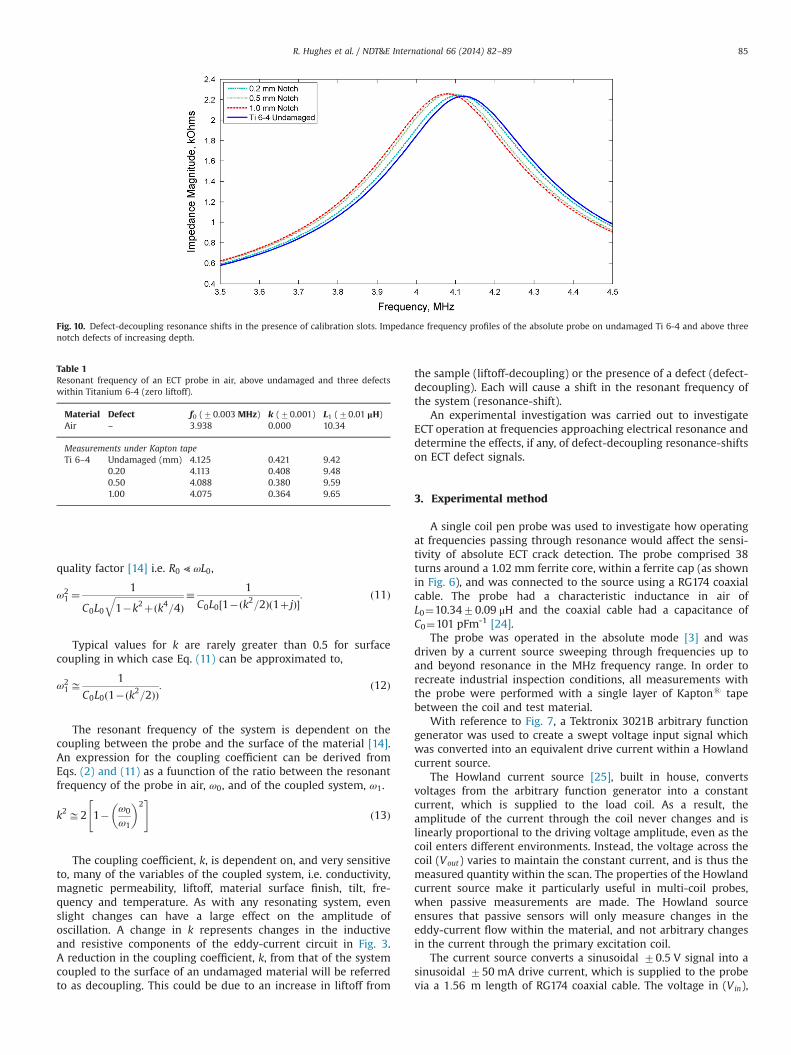
Fig. 10. Defect-decoupling resonance shifts in the presence of calibration slots. Impedance frequency profiles of the absolute probe on undamaged Ti 6-4 and above threenotch defects of increasing depth.
Table 1Resonant frequency of an ECT probe in air, above undamaged and three defectswithin Titanium 6-4 (zero liftoff).
Material Defect f0 (70.003 MHz) k (70.001) L1 (70.01 μH)Air – 3:938 0.000 10.34
Measurements under Kapton tapeTi 6–4 Undamaged (mm) 4.125 0.421 9.42
0.20 4.113 0.408 9.480.50 4.088 0.380 9.591.00 4.075 0.364 9.65
R. Hughes et al. / NDT&E International 66 (2014) 82–89 85
from the function generator, and the voltage across the probe(Vout), were monitored and recorded at a rate of 50 MSamples=susing a National Instruments Labview program (4), which alsocontrolled the XY stage to scan the probe across the sample. Foreach step of the scan, Vin and Vout were recorded over onefrequency sweep, and saved together in a binary file containing
the probe co-ordinates. The ratio of Vout over Vin is proportional tothe impedance, with the knowledge that Vin ¼ IinR.
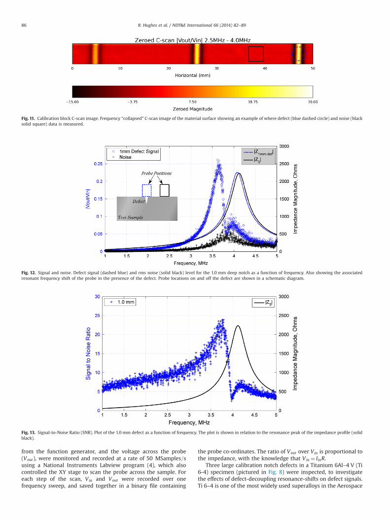
Three large calibration notch defects in a Titanium 6Al–4 V (Ti6-4) specimen (pictured in Fig. 8) were inspected, to investigatethe effects of defect-decoupling resonance-shifts on defect signals.Ti 6–4 is one of the most widely used superalloys in the Aerospace
Fig. 12. Signal and noise. Defect signal (dashed blue) and rms noise (solid black) level for the 1.0 mm deep notch as a function of frequency. Also showing the associatedresonant frequency shift of the probe in the presence of the defect. Probe locations on and off the defect are shown in a schematic diagram.
Fig. 13. Signal-to-Noise Ratio (SNR). Plot of the 1.0 mm defect as a function of frequency. The plot is shown in relation to the resonance peak of the impedance profile (solidblack).
Fig. 11. Calibration block C-scan image. Frequency “collapsed” C-scan image of the material surface showing an example of where defect (blue dashed circle) and noise (blacksolid square) data is measured.
R. Hughes et al. / NDT&E International 66 (2014) 82–8986
industry, and so is an ideal test specimen [1]. The notch defectsspanned the width of the test sample, and had depths of 0.20, 0.50and 1.00 mm (0.008, 0.020 and 0.040 in. respectively). Ti 6–4typically has a conductivity of sTið6�4Þ ¼ 0:60� 106 S m�1 and arelative magnetic permeability μTi ð6�4Þ ¼ 1:00005 [26].
A 4294A Agilent impedance analyzer was used to find theimpedance of the eddy current probe and cable, as a function offrequency, Zðf Þ, of the probe in different environments. Fig. 9shows the Zðf Þ profiles of the probe both on (at zero liftoff withKaptons layer), and off (in air) an undamaged section of the Ti 6–4test piece. The Zðf Þ profiles were also measured for the probepositioned directly above the three notch defects where themaximum frequency shift (defect-decoupling) occurred (Fig. 10).
The resonant frequencies, f 0, for each Zðf Þ profile are shown inTable 1 along with the estimated coupling coefficient, k, calculatedusing Eq. (13), and the equivalent coil inductance, L1, of thesystem, calculated using Eq. (8).
The resonant frequency shifts in Table 1 represent the defect-decoupling of the probe circuit with varying defect size. From thetable, it is clear that the material condition affects the level ofcoupling that can be achieved by the system. It is these changes inthe coupling, and therefore the resonant frequency, which giverise to a signal enhancing phenomenon.
4. Results
Three notches in the Ti 6–4 sample were tested using a singlecoil probe operated in the absolute mode and swept throughfrequencies from 1�5 MHz. A 0:52 ms repeating frequencysweep signal was generated using a 25 MSamples s�1 arbitrary
function generator, to output a driver waveform that satisfies theNyquist criterion.
The waveform was created to decrease exponentially withfrequency (see Fig. 7) so that the Vout signal would not saturatethe measurement scale as the frequency approached resonance.Vin and Vout were scaled such that their maxima, when coupled toundamaged Ti 6–4, were equal to 80% of full screen height.The resulting output signals, Vin and Vout , were convertedinto the frequency domain via Fourier Transform and ‘binned’(bin width¼1923 Hz) over the full frequency range.
The ratio of Vout over Vin is proportional to the impedance ofthe system (Z ¼ Vout=Iin). In this way a value proportional to themagnitude of the ECT defect signals, jZj, was found for eachposition within the XY scan to build an image of the surface. TheC-scan image was zeroed to an area of undamaged material. Fig. 11shows a high contrast C-scan image of the test piece surfaceconstructed by the linear combination of data from frequency binswithin the frequency range of 2:5�4:0 MHz (avoiding resonanceat 4:125 MHz).
At each frequency, the maximum signal strength magnitude,Sðf Þ ¼ jV2=V1j, of each defect and the root-mean squared (rms)noise level, Nrmsðf Þ, of a 10�10 mm2 area of undamaged materialwas recorded from the scan. The data was then plotted as afunction of frequency (Fig. 12), and compared to the impedancemagnitude profiles of the probe on the defect, and on anundamaged section of the material.
It is clear from Fig. 12 that there occurs a frequency, close toresonance, where the defect signal reaches a maximum. Note thatthe background noise reaches a peak at a higher frequency, wherethe defect signal reaches a local minimum. The resulting SNR plotas a function of frequency is shown in Fig. 13 for the 1.0 mm notchdefect.
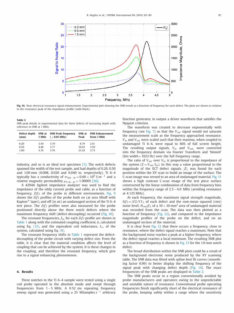
The broad distribution within the SNR plots could be a result ofthe background electronic noise produced by the XY scanningtable. The SNR data was fitted with spline best fit curves (smooth-ing factor 0.99) to better display the shifting frequency of thesignal peak with changing defect depth (Fig. 14). The exactfrequencies of the SNR peaks are displayed in Table 2.
The SNR peaks occur in a region conventionally avoided byprobe manufacturers and operators owing to the unpredictableand unstable nature of resonance. Conventional probe operatingfrequencies finish significantly short of the electrical resonance ofthe probe, keeping safely within a range where the sensitivity
Table 2SNR peak details in experimental data for three defects of increasing depth withreference to SNR at 1 MHz.
Defect depth(mm)
SNR at1 MHz
SNR Peak frequency(70.01 MHz)
SNR atPeak
SNR Enhancementfrom 1 MHz
0.20 3.50 3.79 8.79 2.510.50 4.46 3.77 16.03 3.591.00 5.74 3.76 21.43 3.73
Fig. 14. Near electrical resonance signal enhancement. Experimental plot showing the SNR trends as a function of frequency for each defect. The plots are shown in relationto the resonance peak of the impedance profile (solid black).
R. Hughes et al. / NDT&E International 66 (2014) 82–89 87
scales linearly with frequency due to the inductive reactancecomponent of impedance (ωL).
Beyond resonance, the reactive component of the system isdominated by capacitive changes within the cable, such thatsuccessful measurements of the inductive changes are impossibleso this region must be avoided. Between the conventional limitand the electrical resonance of the system lies a region of probesensitivity dominated by the effects of defect-decoupling reso-nance-shifts, where significant SNR enhancement occurs. This hasbeen termed the Near Electrical Resonance Signal Enhancement(NERSE) frequency band, or zone, and will be dependent on theprobe, cable length, test material and defect size.
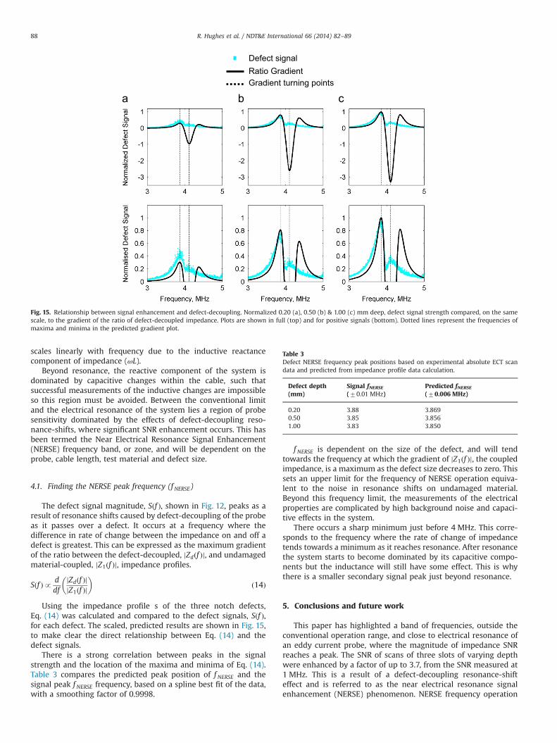
4.1. Finding the NERSE peak frequency (f NERSE)
The defect signal magnitude, Sðf Þ, shown in Fig. 12, peaks as aresult of resonance shifts caused by defect-decoupling of the probeas it passes over a defect. It occurs at a frequency where thedifference in rate of change between the impedance on and off adefect is greatest. This can be expressed as the maximum gradientof the ratio between the defect-decoupled, jZdðf Þj, and undamagedmaterial-coupled, jZ1ðf Þj, impedance profiles.
Sðf Þp ddf
jZdðf ÞjjZ1ðf Þj
� �ð14Þ
Using the impedance profile s of the three notch defects,Eq. (14) was calculated and compared to the defect signals, Sðf Þ,for each defect. The scaled, predicted results are shown in Fig. 15,to make clear the direct relationship between Eq. (14) and thedefect signals.
There is a strong correlation between peaks in the signalstrength and the location of the maxima and minima of Eq. (14).Table 3 compares the predicted peak position of f NERSE and thesignal peak f NERSE frequency, based on a spline best fit of the data,with a smoothing factor of 0.9998.
f NERSE is dependent on the size of the defect, and will tendtowards the frequency at which the gradient of jZ1ðf Þj, the coupledimpedance, is a maximum as the defect size decreases to zero. Thissets an upper limit for the frequency of NERSE operation equiva-lent to the noise in resonance shifts on undamaged material.Beyond this frequency limit, the measurements of the electricalproperties are complicated by high background noise and capaci-tive effects in the system.
There occurs a sharp minimum just before 4 MHz. This corre-sponds to the frequency where the rate of change of impedancetends towards a minimum as it reaches resonance. After resonancethe system starts to become dominated by its capacitive compo-nents but the inductance will still have some effect. This is whythere is a smaller secondary signal peak just beyond resonance.
5. Conclusions and future work
This paper has highlighted a band of frequencies, outside theconventional operation range, and close to electrical resonance ofan eddy current probe, where the magnitude of impedance SNRreaches a peak. The SNR of scans of three slots of varying depthwere enhanced by a factor of up to 3.7, from the SNR measured at1 MHz. This is a result of a defect-decoupling resonance-shifteffect and is referred to as the near electrical resonance signalenhancement (NERSE) phenomenon. NERSE frequency operation
Defect signal Ratio Gradient Gradient turning points
Fig. 15. Relationship between signal enhancement and defect-decoupling. Normalized 0.20 (a), 0.50 (b) & 1.00 (c) mm deep, defect signal strength compared, on the samescale, to the gradient of the ratio of defect-decoupled impedance. Plots are shown in full (top) and for positive signals (bottom). Dotted lines represent the frequencies ofmaxima and minima in the predicted gradient plot.
Table 3Defect NERSE frequency peak positions based on experimental absolute ECT scandata and predicted from impedance profile data calculation.
Defect depth(mm)
Signal fNERSE(70.01 MHz)
Predicted fNERSE(70.006 MHz)
0.20 3.88 3.8690.50 3.85 3.8561.00 3.83 3.850
R. Hughes et al. / NDT&E International 66 (2014) 82–8988
has significant potential for ECT inspection, and opens up a rangeof investigative possibilities. Within this investigation, only themagnitude of the electrical impedance has been analyzed. Animmediate extension of this investigation will be to consider phaseinformation, and determine whether a similar exploitable NERSEeffect exists.
In a break from conventional ECT, the identification of theNERSE frequency band has introduced the possibility of operatingECT probes at a single NERSE frequency (that of a target defect), inorder to increase the probability of detecting smaller defects. Suchan approach could improve the SNR for small defects where, atlower frequencies, the signal from the defect would be below theelectrical background noise. This approach will also be investi-gated for detecting defects within materials of high levels ofmicrostructural background noise. So long as the decouplingresonance-shift caused by the microstructure is less than thatcaused by any defects then a signal enhancement effect should beobserved.
The electrical resonant frequency of an ECT system can beaffected by a number of environmental factors including, but notlimited to; temperature, liftoff, tilt and the degree of surfaceroughness. Operating at frequencies close to resonance will there-fore lead to a greater sensitivity to these issues. However, for anautomated inspection system, i.e. one controlled via roboticmotion, serious liftoff and tilt variations can be suppressed suchthat resonance shifts from these factors are negligible compared toshifts resulting from the presence of defects. In all of the experi-ments carried out, no attempts to limit the effects of temperaturewere made. Variations in the temperature and surface roughnesscan be filtered out using a band-pass filter. So long as these factorsdo not vary in the extreme, so that the level and spatial distribu-tion of resonance shifting they produce is comparable to that ofdefect shifts, the SNR improvement will still be observed. Thesefactors become more of an issue the smaller the target defectbecomes. Future work will investigate the limits of this.
In addition to the use of NERSE frequencies in single coilinspections stated above, there are other promising applicationsfor the additional information sweeping through resonance offers.Sizing and profiling may be possible, by carefully locating the peakfrequency of swept defect signals, and ascertaining the level ofdefect-decoupling associated with a given defect in order todetermine its approximate or relative size. Finally, the complexresonance interactions that occur in densely populated eddy-current arrays (ECAs) will be examined. The focus will be onexploiting the NERSE phenomenon in transmit-receive andarrayed probes in order to achieve greater sensitivity.
The prospect of improving sensitivity through a simple proce-dural change, without the need for complex probe design or dataanalysis, is a potentially valuable complementary technique to anyECT method.
Acknowledgments
Many thanks go to Rolls-Royce plc. and the Research Centre forNon-Destructive Evaluation (RCNDE) for their support, funding
and encouragement. Credit also goes to Rolls-Royce NDE lab,Bristol UK, for the use of the X-Ray CT system.
References
[1] Boyer RR. Titanium for aerospace: rationale and applications. Adv PerformMater 1995;2(4):349–68.
[2] Gros XE, Bousigue J, Takahashi K. NDT data fusion at pixel level. NDT E Int1999;32(5):283–92.
[3] García-Martín J, Gómez-Gil J, Vázquez-Sánchez E. Non-destructive techniquesbased on Eddy current testing. Sensors 2011;11(3):2525–65.
[4] Abu-Nabah B, Hassan W, Ryan D, Blodgett M, Nagy P. The effect of hardness onEddy current residual stress profiling in shot-peened nickel alloys. J. Non-destruct. Eval. 2010;29(3):143–53.
[5] Blodgett MP, Nagy PB. Eddy current assessment of near-surface residual stressin shot-peened nickel-base superalloys. J. Nondestruct. Eval. 2004;23(3):107–23.
[6] Grimberg R, Udpa L, Savin A, Steigmann R, Palihovici V, Udpa SS. 2D Eddycurrent sensor array. NDT E Int 2006;39(4):264–71.
[7] Huang H, Sakurai N, Takagi T, Uchimoto T. Design of an eddy-current arrayprobe for crack sizing in steam generator tubes. NDT E Int 2003;36(7):515–22.
[8] Zilberstein V, Walrath K, Grundy D, Schlicker D, Goldfine N, Abramovici E,et al. MWM eddy-current arrays for crack initiation and growth monitoring.Int J Fatigue 2003;25(9–11):1147–55.
[9] Bartels KA, Fisher JL. Multifrequency eddy current image processing techni-ques for nondestructive evaluation. In: Proceedingsof the International Con-ference onImage Processing; 1995.
[10] Liu Z, Tsukada K, Hanasaki K, Ho YK, Dai YP. Image fusion by using steerablepyramid. Pattern Recogn Lett 2001;22(9):929–39.
[11] Chady T, Sikora R. Optimization of eddy-current sensor for multifrequencysystems. IEEE Trans. Magn. 2003;39(3):1313–6.
[12] Liu Z, Tsukada K, Hanasaki K, Kurisu M. Two-dimensional Eddy current signalenhancement via multifrequency data fusion. Res Nondestruct Eval 1999;11(3):165–77.
[13] Zheng L, Forsyth DS, Komorowski JP, Hanasaki K, Kirubarajan T. Survey: stateof the art in NDE data fusion techniques. Instrum Meas IEEE Trans 2007;56(6):2435–51.
[14] Owston CN. A high frequency eddy-current, non-destructive testing apparatuswith automatic probe positioning suitable for scanning applications. J Phys ESci Instrum 1970;3(10):814.
[15] Liu C, Dong Y. Resonant enhancement of a passive coil-capacitance loop ineddy current sensing path. Measurement 2012;45(3):622–6.
[16] Liu CY, Dong YG. Resonant coupling of a passive inductance-capacitance-resistor loop in coil-based sensing systems. IEEE Sens J 2012;12(12):3417–23.
[17] Ko RT, Blodgett MP, Sathish S., Boehnlein TR. Resonant Frequency Eddy CurrentLiftoff Measurements for Shot Peening Intensity Assessment in Materials, DTICDocument; 2007, (Preprint).
[18] Ko RT, Blodgett MP, Sathish S, Boehnlein TR. Application of resonant frequencyeddy current technique on a shot-peened nickel-based engine-grade material.In: Thompson DO, Chimenti DE. editors. Review of Progress in QuantitativeNondestructive Evaluation. Vol nos. 26A and 26B, American Institute ofPhysics: Melville; 2007. p. 1608–15.
[19] Blitz J. Electrical and magnetic methods of non-destructive testing. London:Chapman & Hall; 1997.
[20] Horowitz P, Hill W. The art of electronics. Cambridge: Cambridge UniversityPress; 1989; 1152.
[21] White JF. High frequency techniques: an introduction to rf and microwaveengineering. New Jersey: Wiley; 2004.
[22] Wheeler HA. Formulas for the skin effect. Proc IRE 1942;30(9):412–24.[23] Bleaney BI, Bleaney B. Electricity and magnetism. Oxford: Oxford University
Press; 1989.[24] RS Online. 13/08/13; Available from: ⟨http://uk.rs-online.com/web/p/coaxial-c
able/5218206/⟩.[25] Anudev, J. and Raglend, I.J. Analytical study of howland current source model.
In: International Conference on. Computing. Electronics and Electrical Tech-nologies (ICCEET); 2012.
[26] Welsch G, Boyer RF, Collings EW. Materials properties handbook: titaniumalloys. Ohio, USA: ASME International; 1994.
R. Hughes et al. / NDT&E International 66 (2014) 82–89 89