nanostructures on c-plane sapphire by the control of ... · figure s4: evolution of round-dome...
TRANSCRIPT

1
Supporting Information
Determination of growth regimes of Pd
nanostructures on c-plane sapphire by the control of
deposition amount at different annealing
temperature
Sundar Kunwar1, Mao Sui1, Puran Pandey1, Quanzhen Zhang1, Ming-Yu Li1, Harish Bhandari1,
and Jihoon Lee1,2*
1College of Electronics and Information, Kwangwoon University, Nowon-gu Seoul 01897, South Korea
2Institute of Nanoscale Science and Engineering, University of Arkansas, Fayetteville AR 72701, USA.
Correspondence e-mail: [email protected]
Electronic Supplementary Material (ESI) for Physical Chemistry Chemical Physics.This journal is © the Owner Societies 2017

2
Figure S1: Raman spectra of 430 µm thick bare sapphire (0001) measured at room temperature by the excitation of 532 nm laser. Six active Raman modes from the sapphire (0001) at 377.3, 416.3, 428.1, 447.6, 575.8 and 749.3 cm-1 were detected and peak positions are denoted by the arrows. The peak at 416.3 cm-1 is due to the A1g vibration mode whereas the others are due to the Eg vibration modes of sapphire. Different power levels were used to obtain the Raman spectra as denoted. Low intensity vibration modes are clearly detected with high power.

3
Figure S2: (a) – (r) AFM top-views of 3 × 3 µm2 showing pre-annealed Pd deposition on sapphire (0001) ranging from 0.5 to 200 nm. (b) RMS roughness (Rq). (c) Surface area ratio (SAR). Generally, the Pd atoms were uniformly distributed and the surface roughness is monotonously increased with the deposition thickness. The specific values of RMS roughness and SAR are listed in table S1.

4
Figure S3: Cross-sectional line profiles of the AFM top-views in Fig. S2. The surface roughness as well as the thickness range is gradually increased as shown by the cross-sectional line profiles.

5
Figure S4: Evolution of round-dome shaped Pd NPs on sapphire at 850 oC for 450s with the variation of the deposition amount from 1 to 40 nm. (a) – (h) 3-D AFM side views of 3 × 3 µm2. The corresponding color scale bars represent the height information.

6
Figure S5: Small to large sized self-assembled Pd NPs on sapphire (0001) with 1 – 40 nm thick Pd films at 850 oC for 450 s. (a) – (h) 3-D AFM side-views of 1 × 1 µm2. The corresponding scale bars represent the height with color variation.
7
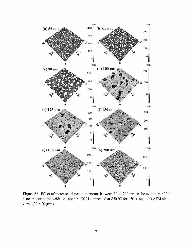
Figure S6: Effect of increased deposition amount between 50 to 200 nm on the evolution of Pd nanostructures and voids on sapphire (0001), annealed at 850 ºC for 450 s. (a) – (h) AFM side-views (20 × 20 µm2).

8
Figure S7: Formation of voids and their evolution with the deposition of Pd between 50 – 200 nm after annealing at 850 oC for 450 s. (a) – (d) AFM top-views of 5 × 5 µm2. (a-1) – (d-1) Cross-sectional line profiles. (a-2) – (d-2) FFT power spectra. (a-3) – (d-3) Corresponding 3-D AFM side-views.

9
Figure S8: Morphological evolution of Pd NPs on sapphire at 800 oC for 450 s by the thickness variation of Pd between 1 and 40 nm. (a) – (h) AFM side views of 3 × 3 µm2

10
Figure S9: Enlarged 3-D AFM side views of 1 × 1 µm2 showing the self-assembled Pd NPs at 800 oC for 450 s between 1 and 40 nm.

11
Figure S10: EDS spectra of the Pd nanostructures on sapphire (0001), annealed at 800 °C for 450 s with various thickness of Pd layers. Full range EDS spectra of samples with thickness (a) 1 - 10 nm and (b) 15 - 40 nm. (a-1) – (b-1) Enlarged spectra of selected region between 2.6 – 3.2 keV showing Pd Lα1 and Pd Lβ1. (c) EDS count plot as a function of deposition amount.

12
Figure S11: Raman spectra between 400 and 440 cm-1 showing the A1g vibration modes for the samples with the Pd thickness from 1 to 40 nm annealed at 800 oC for 450 s.(b) – (d) Peak intensity, peak shift and full width at half maximum (FWHM) plots with respect to the deposition amount.

13
Figure S12: Reflectance spectra of Pd nanoparticles on sapphire (0001) fabricated with the deposition amount variation between 1 and 40 nm at 800 °C for 450 s: (a) bare sapphire, (b) – (i) samples with deposition amount as depicted. (j) Summary plot of average reflectance.

14
Figure S13: Formation of small to large sized self-assembled Pd NPs at 750 oC for 450 s along with the deposition amounts variation from 1 to 40 nm. (a) – (h) AFM top-views of 3 × 3 µm2.

15
Figure S14: Evolution of small to medium sized self-assembled Pd NPs on sapphire, annealed at 750 oC for 450 s by the deposition amount variation between 1 and 10 nm. (a) – (d) AFM side-views of 1 × 1 µm2. (a-1) – (d-1) Corresponding AFM top-views. (a-2) – (d-2) Cross-sectional line profiles. (a-3) – (d-3) 2-D - FFT power spectra.

16
Figure S15: Formation of medium to large sized self-assembled Pd NPs on sapphire by the deposition variation between 15 and40 nm annealed at 750 oC for 450 s. (a) – (d) AFM side-views of 1 × 1 µm2. (a-1) – (d-1) Corresponding AFM top-views. (a-2) – (d-2) Cross-sectional line profiles. (a-3) – (d-3) 2-D - FFT power spectra.

17
Figure S16: Scanning electron microscope (SEM) images of voids formed on Pd layers at 750 oC for 450 s with the deposition thickness from 50 to 200 nm.

18
Figure S17: EDS spectra of Pd NPs on sapphire with the deposition amount variation between 1 and 40 nm and annealed at 750 oC for 450 s. (a) – (b) Full range spectra of the samples. (a-1) – (b-1) Enlarged view of the selected area. (c) Spectral counts of the Pd Lα1 as a function of deposition amount.

19
Figure S18: EDS spectra of samples with the deposition amount between 50 and 200 nm, annealed at 750 oC for 450 s. (a) – (b) Full range spectra of the samples. (a-1) – (b-1) Enlarged spectra. (c) Spectral counts of the Pd Lα1.

20
Figure S19: Raman spectra of Pd NPs at 750 oC for 450 s with the deposition amounts from 1 to 40 nm. (a) Spectral range of 400 to 440 cm-1. (b) Plot of peak intensity, (c) peaks shift and (d) FWHM.
21
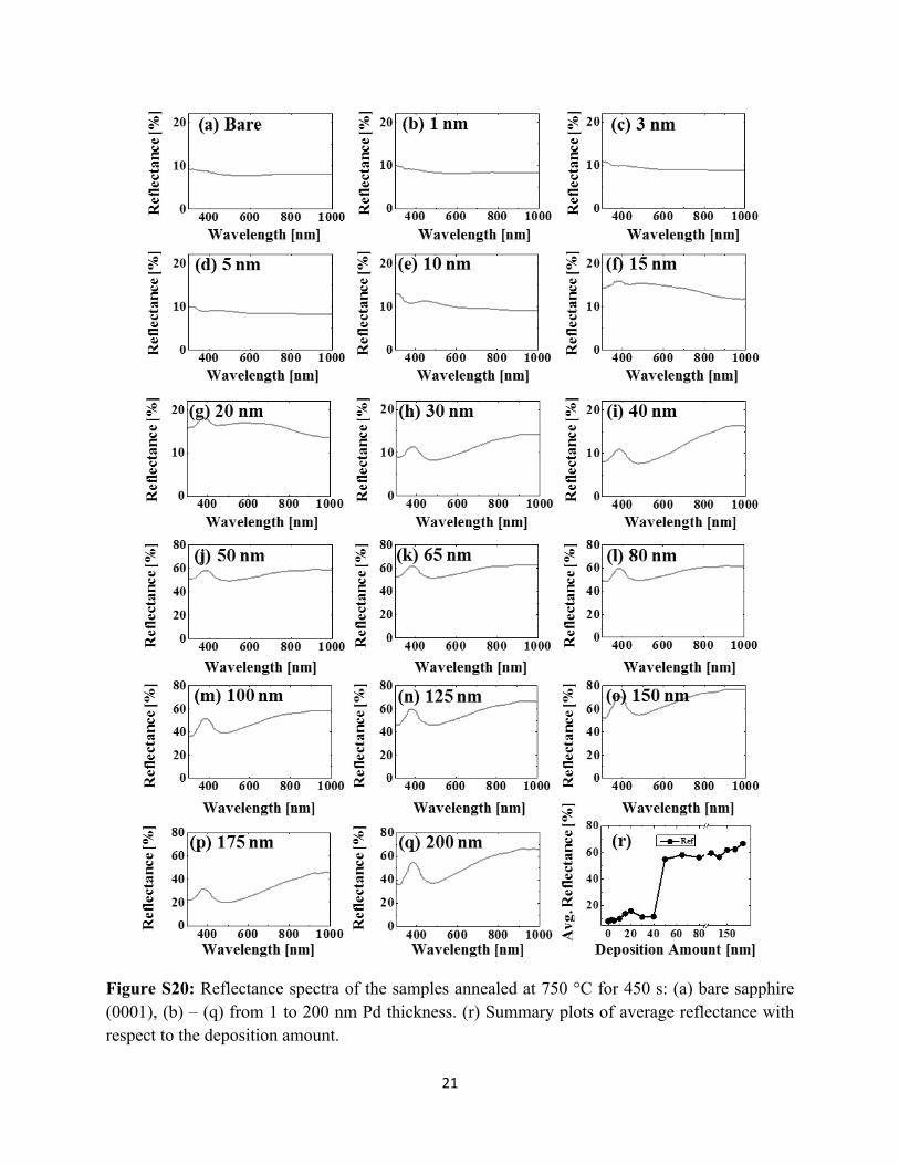
Figure S20: Reflectance spectra of the samples annealed at 750 °C for 450 s: (a) bare sapphire (0001), (b) – (q) from 1 to 200 nm Pd thickness. (r) Summary plots of average reflectance with respect to the deposition amount.

22
Table S1: Summary of RMS roughness (Rq) and surface area ratio (SAR) of Pd deposited samples before annealing after deposition with the deposition amount between 0.5 and200 nm.
Deposition Amount [nm] Rq [nm] SAR [%]
0.5 0.215 0.028
1 0.264 0.046
2 0.177 0.017
3 0.192 0.033
5 0.358 0.128
7 0.614 0.776
10 0.862 1.754
15 1.197 1.850
25 1.425 1.978
50 1.590 2.050
65 1.682 2.112
75 1.975 2.820
80 2.801 4.320
100 3.615 6.934
125 4.556 9.813
150 5.371 12.506
175 6.337 12.698
200 6.917 13.478

23
Table S2: Summary of Rq and SAR related to the Pd NPs fabricated on sapphire with the control of deposition amount at various annealing temperatures (fabrication at 750 - 850oC for 450 s).
Temperature
750 oC 800 oC 850 oCDeposition Amounts
[nm] SAR [%] Rq [nm] SAR [%] Rq [nm] SAR [%] Rq [nm]
1 0.251 0.748 0.642 0.957 0.208 0.674
3 0.923 1.047 2.594 2.119 1.155 1.144
5 7.053 6.601 6.583 6.849 5.300 4.919
10 7.212 12.110 10.311 11.235 11.970 10.973
15 8.283 14.394 9.3080 14.698 10.405 15.169
20 8.223 16.081 9.030 17.24 9.714 16.875
30 7.205 28.605 8.187 24.798 9.168 24.753
40 9.496 34.641 10.046 30.181 10.541 26.054
50 1.087 3.121 - - 8.565 45.731
65 1.044 2.745 - - 9.337 56.782
80 1.683 3.118 - - 6.117 47.635
100 2.850 6.301 - - 3.384 13.49
125 2.003 3.945 - - 4.029 18.48
150 4.156 7.055 - - 4.877 8.115
175 4.108 5.689 - - 5.540 9.266
200 5.258 9.341 - - 6.829 11.228

24
Table S3: Summary of the average height (AH), average lateral diameter (LD) and average density (AD) of round dome-shaped Pd NPs on sapphire as a function of deposition amount of 1 – 40 nm (fabrication at 750 - 850oC for 450 s).
750 oC 800 oC 850 oC
Deposition Amounts
[nm] AH[nm]
LD[nm]
AD[× 108/cm2]
AH[nm]
LD[nm]
AD[× 108
/cm2]
AH[nm]
LD[nm]
AD[× 108
/cm2]
1 2.64 20.55 953 2.9 20.68 911 3.2 30.32 504
3 4.28 31.19 831 6.58 26.2 818 6.64 37.38 394
5 11.69 51.31 260 13.92 59.34 188 12.78 59.16 154
10 25.11 75.13 48 28.74 88.77 42 29.54 101.86 43.89
15 37.84 130.44 15.55 40.87 132.66 18.33 38.25 142.22 16
20 45.54 175.35 14 53.62 195.5 16.33 47.44 173.93 14
30 61.52 225.43 6.78 73.96 238.75 5.89 66.44 238.51 5.78
40 109.44 340.12 2.33 93.31 312.98 3.33 80.04 305.43 3.56

25
Table S4: Summary of Raman intensity (I), peak position (PP) and full width at half maximum (FWHM) of Pd nanostructures fabricated on sapphire (0001) with the control of deposition amounts from 1 to 80 nm at 750, 800 and 850 oC for 450 s.
750 oC 800 oC 850 oCDeposition Amounts
[nm] I PP[/cm]
FWHM[/cm] I PP
[/cm]
FWHM
[/cm]I PP
[/cm]
FWHM
[/cm]
Bare 2636.27 416.47 7.557 2636.27 416.47 7.557 2636.27 416.47 7.557
1 2550.63 415.49 7.426 2488.84 416.42 7.543 2513.16 415.25 7.325
3 2430.92 415.47 7.533 2305.76 416.32 7.796 2444.08 415.24 7.397
5 2304.91 415.47 7.363 2161.82 416.39 7.555 2187.32 415.34 7.425
10 1787.25 415.49 7.423 1268.70 415.80 7.506 1801.85 415.22 7.324
15 1164.26 415.34 7.432 1170.00 416.00 7.407 1264.94 415.14 7.399
20 974.28 415.39 7.305 1072.48 415.96 7.499 1051.17 415.04 7.584
30 1000.69 415.24 7.539 1236.95 415.97 7.383 1090.54 415.02 7.256
40 952.74 415.31 7.401 1017.35 415.92 7.366 1005.64 415.07 7.346
50 - - - - - - 983.87 414.94 7.453
65 - - - - - - 826.86 414.93 7.271
80 - - - - - - 645.61 414.81 7.460

26
Table S5: Summary of the average reflectance for the samples with various Pd deposition amount from 1 to 200 nm after annealing at distinct temperatures: 750, 800 and 850 °C for 450 s.
Reflectance [%]Deposition Amounts
[nm] 750 °C 800 °C 850 °C
Bare 8.13 8.47 8.38
1 8.51 8.24 8.46
3 9.20 8.89 8.57
5 8.61 9.95 8.90
10 10.06 10.35 13.27
15 13.97 14.45 13.37
20 15.98 17.18 10.40
30 11.29 13.36 9.75
40 11.69 16.08 10.24
50 54.85 - 11.59
65 58.11 - 12.02
80 56.24 - 13.56
100 59.59 - 47.53
125 56.56 - 50.43
150 61.77 - 52.01
175 62.29 - 54.82
200 66.80 - 55.84