nanostructured thin films for solid oxide fuel cells · solid oxide fuel cell (tf-sofc) cathodes by...
TRANSCRIPT
NANOSTRUCTURED THIN FILMS FOR SOLID OXIDE FUEL CELLS
A Dissertation
by
JONGSIK YOON
Submitted to the Office of Graduate Studies of Texas A&M University
in partial fulfillment of the requirements for the degree of
DOCTOR OF PHILOSOPHY
December 2008
Major Subject: Electrical Engineering
NANOSTRUCTURED THIN FILMS FOR SOLID OXIDE FUEL CELLS
A Dissertation
by
JONGSIK YOON
Submitted to the Office of Graduate Studies of Texas A&M University
in partial fulfillment of the requirements for the degree of
DOCTOR OF PHILOSOPHY
Approved by:
Chair of Committee, Haiyan Wang Committee Members, Jim Ji Frederick Strieter Xinghang Zhang Head of Department, Costas N. Georghiades
December 2008
Major Subject: Electrical Engineering
iii
ABSTRACT
Nanostructrued Thin Films for Solid Oxide Fuel Cells.
(December 2008)
Jongsik Yoon, B.S., Yonsei University, Korea;
M.S., University of Southern California
Chair of Advisory Committee: Dr. Haiyan Wang
The goals of this work were to synthesize high performance perovskite based thin film
solid oxide fuel cell (TF-SOFC) cathodes by pulsed laser deposition (PLD), to study the
structural, electrical and electrochemical properties of these cathodes and to establish
structure-property relations for these cathodes in order to further improve their properties
and design new structures.
Nanostructured cathode thin films with vertically-aligned nanopores (VANP) were
processed using PLD. These VANP structures enhance the oxygen-gas phase diffusivity,
thus improve the overall TF-SOFC performance. La0.5Sr0.5CoO3 (LSCO) and
La0.4Sr0.6Co0.8Fe0.2O3 (LSCFO) were deposited on various substrates (YSZ, Si and
pressed Ce0.9Gd0.1O1.95 (CGO) disks). Microstructures and properties of the
nanostructured cathodes were characterized by transmission electron microscope (TEM),
high resolution TEM (HRTEM), scanning electron microscope (SEM) and
electrochemical impedance spectroscopy (EIS) measurements.
iv
A thin layer of vertically-aligned nanocomposite (VAN) structure was deposited in
between the CGO electrolyte and the thin film LSCO cathode layer for TF-SOFCs. The
VAN structure consists of the electrolyte and the cathode materials in the composition of
(CGO) 0.5 (LSCO) 0.5. The self-assembled VAN nanostructures contain highly ordered
alternating vertical columns formed through a one-step thin film deposition using a PLD
technique. These VAN structures significantly increase the interface area between the
electrolyte and the cathode as well as the area of active triple phase boundary (TPB),
thus improving the overall TF-SOFC performance at low temperatures, as low as 400oC,
demonstrated by EIS measurements. In addition, the binary VAN interlayer could act as
the transition layer that improves the adhesion and relieves the thermal stress and lattice
strain between the cathode and the electrolyte.
The microstructural properties and growth mechanisms of CGO thin film prepared by
PLD technique were investigated. Thin film CGO electrolytes with different grain sizes
and crystal structures were prepared on single crystal YSZ substrates under different
deposition conditions. The effect of the deposition conditions such as substrate
temperature and laser ablation energy on the microstructural properties of these films are
examined using XRD, TEM, SEM, and optical microscope. CGO thin film deposited
above 500 ºC starts to show epitaxial growth on YSZ substrates. The present study
suggests that substrate temperature significantly influences the microstructure of the
films especially film grain size.

v
DEDICATION
To my beloved parents and brother, to my teachers, and to my friends

vi
ACKNOWLEDGMENTS
I would like to express my deepest gratitude to my graduate advisor Dr. Haiyan Wang
for her invaluable advice, financial support, and especially for her academic guidance. I
am deeply indebted to my advisor whose help, stimulating suggestions and
encouragement helped me in all the time of research and writing this dissertation. Dr.
Haiyan Wang is one of the best professors that I have met in my life. She sets high
standards for her students and she encourages and guides us to meet those standards. Her
teachings greatly inspired me during my graduate study.
I would like to thank Profs. Frederick Strieter, Jim Ji, Xing Cheng, and Xinghang Zhang
for serving as my committee members. I acknowledge their helpful comments and
suggestions in shaping this dissertation. I wish to thank Dr. Adriana Serquis in the
Centro Atomico Bariloche, Argentina for the helpful discussion about impedance
analysis and valuable contributions to the papers we wrote together. I wish to take this
opportunity to acknowledge Dr. Susan Wang at the University of Houston for sharing
her profound knowledge and experience about microstructure characterization and
impedance measurement. I also thank Joon Hwan Lee for his late night presence
whenever I did PLD depositions. I thank my girl friend Soonyoung for her constant
support.

vii
I would like to acknowledge financial support from the Air Force Office of Scientific
Research and also from the State of Texas through the Texas Engineering Experiment
Station. I am grateful to the University of Houston and Centro Atomico Bariloche,
Argentina research group for measuring the ASR, and impedance data.
Finally, I want to thank my friends in the thin film characterization group, Ickchan Kim,
Roy Araujo, Zhenxing Bi, Joyce Wang, Joonhwan Lee, Chen-Fong Cho, Song Du, and
Sungmee Cho, for making my graduate years enjoyable and memorable. The facilities
and resources provided by the Electrical and Computer Engineering Department, Texas
A&M University, are gratefully acknowledged. I thank Texas A&M University,
University of Southern California and Yonsei University for educating me in various
ways.
viii
TABLE OF CONTENTS
Page
CHAPTER I INTRODUCTION ………………….…………………………………1
1.1 Overview………………………………………………………….1 1.2 Fuel Cells………………………………………………….…….3
1.2.1 Origin of Fuel Cells …………...............................4 1.2.2 Fuel Cell Types…………………………………...5
1.3 Solid Oxide Fuel Cells (SOFCs) ………………………………....7 1.3.1 History of SOFCs………………………………...9 1.3.2 SOFC Operating Mechanism …………………10
1.4 Materials for SOFC Components……………………………….12 1.4.1 Cathode …………………………………..16 1.4.2 Anode……………………………………………18 1.4.3 Electrolyte……………………………………….20
1.5 SOFC Cell Configurations………………………………………21 1.6 SOFC Limitations and Thin Film Approach……………………25 1.7 Future Work for SOFCs…………………………………………26 1.8 Summary………………………………………………………...28
CHAPTER II RESEARCH METHODOLOGY …………………………………30
2.1 Pulsed Laser Deposition (PLD) Technique……………………..30 2.1.1 Interaction of the Laser Beam with the Target….34 2.1.2 Interaction of the Laser Beam with Evaporated
Materials………………………………………...37 2.1.3 Adiabatic Plasma Expansion and Thin Film
Deposition……………………………………….42 2.2 Characterization Methods of Thin Films………………………..43
2.2.1 X-ray Diffraction………………………………..44 2.2.2 Transmission Electron Microscopy
(Structural: TEM)…………………………….....54 2.2.3 Scanning Transmission Electron Microscopy
(STEM): Structural and Elemental Analysis Using Z-Contrast………………………………..67
2.2.4 Electrochemical Impedance Spectroscopy……...73
ix
Page
CHAPTER III NANOSTRUCTURED CATHODE THIN FILMS WITH
VERTICALLY-ALIGNED NANOPORES FOR THIN FILM
SOFC AND THEIR CHARACTERISTICS……...…………………..89
3.1 Overview………………………………………………………...89 3.2 Introduction……………………………………………………...90 3.3 Experimental ……………………………………………………91 3.4 Results and Discussion ……………………………………….92 3.5 Summary……………………………………………………….101
CHAPTER IV VERTICALLY ALIGNED NANOCOMPOSITE THIN FILM AS
CATHODE ELECTROLYTE INTERFACE LAYER FOR
THIN FILM SOLID OXIDE FUEL CELLS………………...………102
4.1 Overview……………………………………………………….102 4.2 Introduction……………………………………………………103 4.3 Experimental…………………………………………………...105 4.4 Results and Discussion………………………………………107 4.5 Summary……………………………………………………….119
CHAPTER V MICROSTRUCTURAL STUDY OF THIN FILM
Ce0.90Gd0.10O1.95 (CGO) AS ELECTOROLYTE FOR SOLID
OXIDE FUEL CELL APPLICATIONS……………………………121
5.1 Overview……………………………………………………….121 5.2 Introduction…………………………………………………….122 5.3 Experimental…………………………………………………...124 5.4 Results and Discussion……………………………………....127 5.5 Summary………………………………………………………133
CHAPTER VI SUMMARY…………………………………………………………..135
REFERENCES………………………………………………………………………137
VITA…………………………………………………………………………………147
x
LIST OF TABLES
TABLE Page
1.1 Summary of the five main types of fuel cells and their characteristics…………6
1.2 The electrochemical reaction on each electrode in SOFC……………………..12
1.3 Physical properties of selected SOFC components…………………………….16
1.4 SOFC application goals until year 2010……………………………………….27
4.1 List of VAN layer thicknesses and the ratio of the interface area density between with and without VAN layer for different samples………………....111
5.1 Typical deposition parameters………………………………………………126
5.2 Film thicknesses and growth rate at different temperatures………………….132
xi
LIST OF FIGURES
FIGURE Page
1.1 Global–mean temperature change over the period of 1990–2100 and 1990–2030………………………………………………………………………..2
1.2 Volume of oil discovered world wide every five years…………………………3
1.3 Schematic diagram of SOFC operating on hydrogen fuel………………………..9
1.4 Schematic diagram showing the general operating principles of SOFC………11
1.5 Schematic diagram of SOFC based on proton (hydrogen ion) conductors……..14
1.6 Schematic diagram of SOFC with oxygen ion conductors……………………14
1.7 (a) Perovskite (ABO3) structured electrode and (b) face centered cubic structure of CGO electrolyte…………………………………………………...15
1.8 Tubular type SOFC configuration………………………………………………22
1.9 Planar unit cell design of SOFC single stack with bipolar interconnects………23
1.10 Schematic diagram of thin film SOFC…………………………………………26
2.1 Schematic diagram of the pulsed laser deposition system………………………32
2.2 Schematic representation of the stages of laser target interactions during short pulse high power laser interaction with a solid…………………………..34
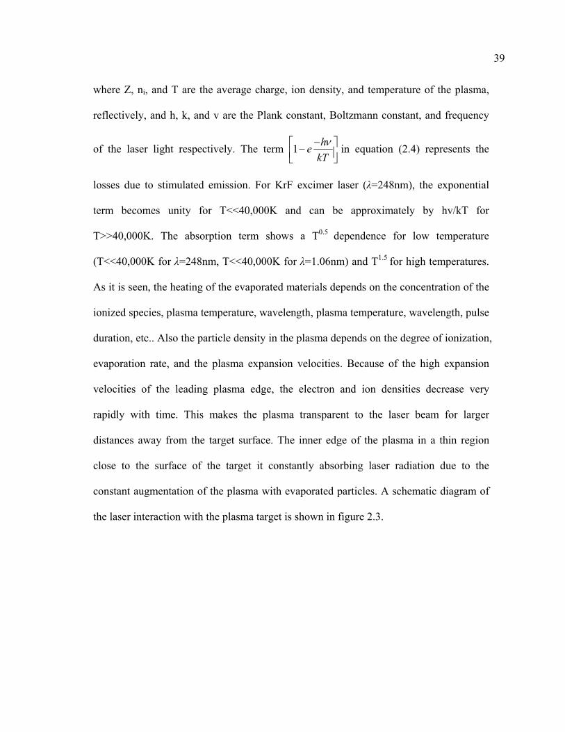
2.3 Schematic diagram representing the different phases present during irradiation of a laser on a bulk target…………………………………………40
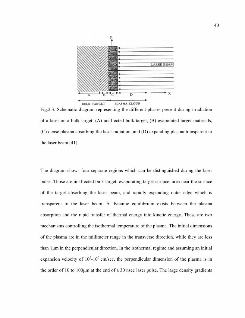
2.4 Schematic profile showing the density (n), pressure (P), and velocity (v) gradients in the plasma in x direction, normal to the target surface……………41
2.5 Schematic of X-ray spectrometer…………………………………………….....45
2.6 Effect of fine particle size on diffraction curve…………………………………46
xii
FIGURE Page
2.7 The atomic scattering factor of copper………………………………………….49
2.8 Lorentz-polarization factor vs. Bragg angle…………………………………….51
2.9 Effect of lattice strain on the line width and position…………………………53
2.10 Objective aberration (a) Spherical, (b) chromatic, (c) astigmatism…………......57
2.11 The two basic operations of the TEM imaging system involve (A) Projecting the diffraction pattern on the viewing screen and (B) projecting the image onto the screen………………………………………………………59
2.12 Ray diagrams showing how the objective lens aperture are used in combination to produce (A) a BF image formed from the direct beam, (B) a displaced-aperture DF image formed with a specific off-axis scattered beam, and (C) a CDF image where the incident beam is tilted so that the scattered beam remains on axis…………………………………………………………61
2.13 Phase contrast imaging from a periodic object. The diffracted and transmitted beams recombine at the image plane…………………………………………63
2.14 Schematic representation of TEM as a transmission system……………………64
2.15 Scanning the convergent probe for STEM image formation using two pairs of scan coils between the C2 lens and the upper objective polepiece………….68
2.16 STEM image formation…………………………………………………………71
2.17 SOFC single cell configuration…………………………………………………74
2.18 A Lissajous ellipse is observed on an X-Y recorder when a sine wave voltage is superimposed on the dc polarization voltage………………………77
2.19 Three-electrode measurement configuration and a schematic Nyquist impedance diagram…………………………………………………………….83
2.20 AC impedance of a SOFC. (a) Nyquist diagram of Impedance Z and (b) bode plot of impedance ‘Z’………………………………………………84
2.21 (a) Whole cell with a two-electrode configuration and (b) the corresponding Nyquist plot…………………………………………………….88
xiii
FIGURE Page
3.1 SEM images of (a) cross-sectional view and (b) low and (c) high magnifications of surface morphology of a LSCO cathode grown by PLD on Si substrate………………………………………………………………….93
3.2 SEM images of (a) cross-section surface of LSCFO on Si substrate deposited at the same run with LSCFO on CGO disks, and (b) its corresponding surface SEM……………………………………………………95
3.3 Low magnification cross-section TEM image of one such porous LSCO on Si substrates with vertical-aligned nanopores………………………………97
3.4 Arrhenius plot of area specific resistance (ASR) of LSCFO layer with VANP structure (stars) and other cathodes reported in literature by Dusastre et al…………………………………………………………………...98
3.5 Complex impedance spectra under different pO2 values (ranging from 1 atm to 10-3 atm)……………………………………………………………...99
4.1 (a) Schematic diagram of a symmetric cell and (b) VAN interlayer where “L” and “C” stand for LSCO and CGO columns, respectively………105
4.2 Cross-sectional (a) low magnification and (b) high resolution TEM images, and (c) STEM image of a typical LSCO/CGO VAN structure grown by PLD on STO substrate……………………………………………107
4.3 (a) Low magnification cross-sectional TEM image of a LSCO cathode and VAN interlayer on a pressed CGO disk, (b) a closer view of the VAN interlayer structure on the CGO disk, and (c) SEM image showing a smooth surface of the cathode layer without microcrack formation……………………………………………………………………...113
4.4 Criteria adopted for electrode polarization resistance determination…………115
4.5 ASR of symmetrical cells with VANP/VAN structures on CGO disks grown by PLD………………………………………………………………117
5.1 XRD patterns of Ce0.9Gd0.1O1.95 thin film deposited on YSZ substrate at different temperatures……………………………………………128
5.2 Optical images of microstructure of as deposited CGO thin films deposited at (a) RT, (b) 300 ºC, (c) 500 ºC, and (d) 700 ºC on YSZ substrates……………………………………………………………………...130
xiv
FIGURE Page
5.3 Low magnification cross section TEM images of CGO thin films deposited at (a) RT, (b) 300 ºC, (c) 500 ºC, and (d) 700 ºC……………………………..131
5.4 Film growth rate vs. deposition temperature…………………………………132
5.5 High magnification crossection TEM images of CGO thin films deposited at (a) RT, (b) 300 ºC, (c) 500 ºC, and (d) 700 ºC…………………134
1
CHAPTER I
INTRODUCTION
This chapter presents the motivation and objectives of the research in this dissertation.
Solid oxide fuel cell (SOFC) is one of the most promising energy sources which are
clean and highly efficient. However due to the high operating temperature, developing
cost effective SOFCs is a challenging task. Literature review in this chapter summarizes
historical developments of the fuel cells with special emphasis on SOFC. Finally, future
work is proposed.
1.1 Overview
Fuel cells are one of the most efficient, environmentally clean and effective energy
sources which convert chemical energy of a fuel gas directly into electrical energy. It is
now well understood that global warming is taking place mainly due to carbon dioxide
(CO2) gas emission from fossil fuel combustion. In the past century, global temperature
has increased at a rate near 0.6°C/century [1]. For the past 25 years this trend has
increased dramatically. According to the US Department of Energy (DoE), by 2015
world carbon emissions are expected to increase 54% more than 1990 emission and this
___________ This dissertation follows the style and format of the Applied Surface Science.
2
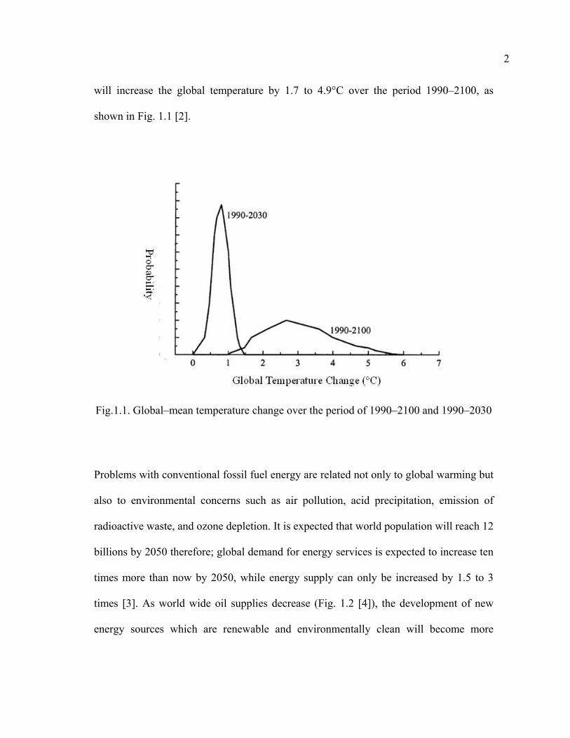
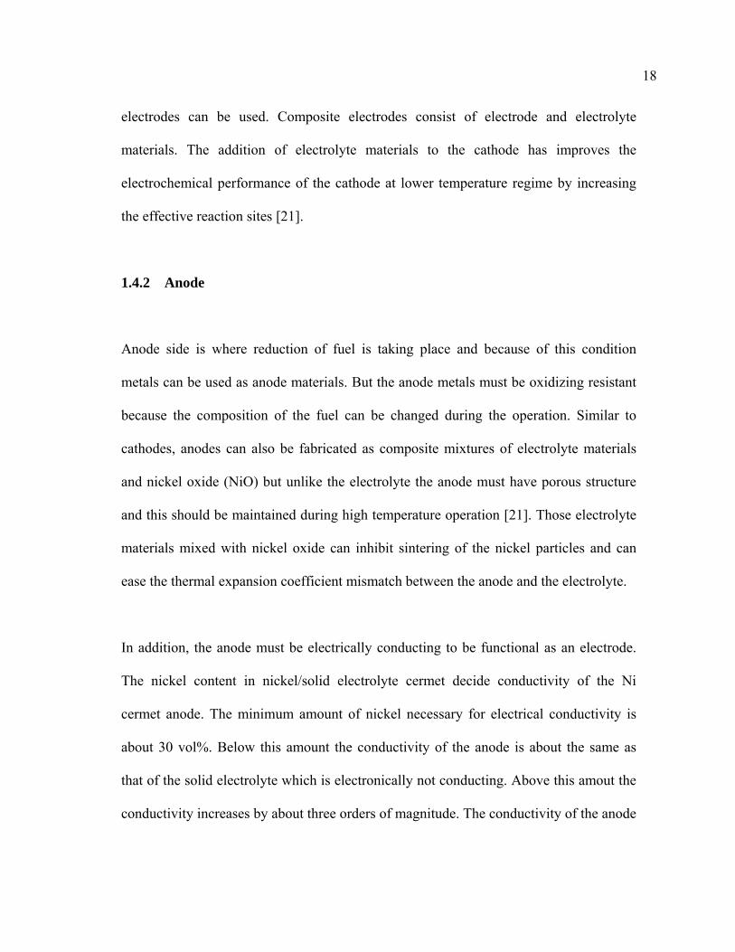
will increase the global temperature by 1.7 to 4.9°C over the period 1990–2100, as
shown in Fig. 1.1 [2].
Fig.1.1. Global–mean temperature change over the period of 1990–2100 and 1990–2030
Problems with conventional fossil fuel energy are related not only to global warming but
also to environmental concerns such as air pollution, acid precipitation, emission of
radioactive waste, and ozone depletion. It is expected that world population will reach 12
billions by 2050 therefore; global demand for energy services is expected to increase ten
times more than now by 2050, while energy supply can only be increased by 1.5 to 3
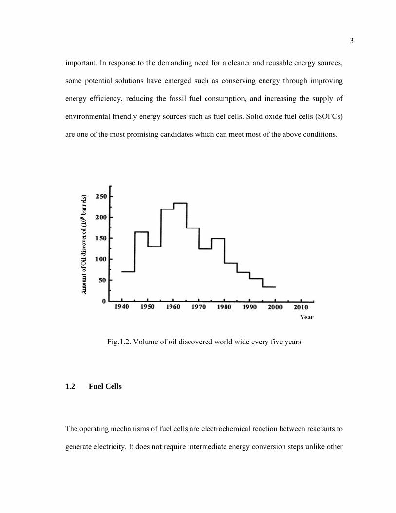
times [3]. As world wide oil supplies decrease (Fig. 1.2 [4]), the development of new
energy sources which are renewable and environmentally clean will become more
3
important. In response to the demanding need for a cleaner and reusable energy sources,
some potential solutions have emerged such as conserving energy through improving
energy efficiency, reducing the fossil fuel consumption, and increasing the supply of
environmental friendly energy sources such as fuel cells. Solid oxide fuel cells (SOFCs)
are one of the most promising candidates which can meet most of the above conditions.
Fig.1.2. Volume of oil discovered world wide every five years
1.2 Fuel Cells
The operating mechanisms of fuel cells are electrochemical reaction between reactants to
generate electricity. It does not require intermediate energy conversion steps unlike other
4
electric power generation devices such as internal combustion engines. Because of its
simple direct energy conversion mechanism it shows much higher efficiency than
conventional method. Fuel cells can operate as long as both fuel and oxidant are supplied
to the electrodes.
1.2.1 Origin of Fuel Cells
Fuel cells have been known for more than 160 years and have been researched
intensively since World War II. Alessandro Volta (1745–1827) was the first scientist
who first observed the electrical phenomena. J. W. Ritter (1776–1810), also known as
the founder of the electrochemistry, has continued to develop the understanding of
electricity. In 1802, Sir Humphrey Davy created a simple fuel cell based upon a C/H2O
and NH3/O2/C compounds delivering a week electric power. The fuel cell principle was
discovered by Christan Friedrich Schonbein during 1829 to 1868. Sir William Grove
(1811–1896) developed an improved wet cell battery (‘Grove cell’) in 1838. This cell
type is based on the backward reaction of the electrolysis of water [5]. Nernst discovered
solid oxide electrolytes much later in 1899 and this introduced ceramic fuel cells [6].
Ludwig Mond (1839–1909) spent most of his time in developing industrial chemical
technology. Mond and his assistant Carl Langer developed a hydrogen–oxygen fuel cell
that generated 6 amps per square foot of the electrode at 0.73 V. The theoretical
understanding of how fuel cells operate was decribed by V. Friedrich Wilhelm Oswald
(1853-1932). During the first half of the 20th century Emil Baur (1873–1944) researched
5
many different types of fuel cells. Baur’s work includes high temperature molten silver
electrolyte devices and a unit that used a solid electrolyte of clay and metal oxides.
Francis Thomas Bacon (1904–1992) initiated alkali electrolyte fuel cells research in the
late 1930s. Since 1945, three research groups (US, Germany and the former USSR) took
over the studies on some principal types of generators by improving their technologies
for industrial development purposes [7]. In 1960, NASA supported hydrogen based fuel
cell research and successfully developed to supply power to the electrical systems on the
Apollo. Although it was discovered over 160 years ago with all the facts that it is
environmentally clean and the efficiency is as high as over 70% only now fuel cell
technology is close to commercialization because of its high cost components and high
operating temperature. However due to the extensive research for the last two decades
on materials science and process technologies now we are on the verge of its realization
as a alternate, clean energy source. Today, fuel cells are widely adopted in many
applications such as space shuttle, transportation, possible use as portable power system,
remote power generation and intermediate size distributed power generation.
1.2.2 Fuel Cell Types
There is now many different types of fuel cells available. The main differences among
them are their chemical characteristics of the electrolytes in the cell. However, the basic
operating principle of all types of fuel cell is the same. Depending on the electrolyte,
either protons or oxide ions are transported through the electrolyte. Electrons transported
6
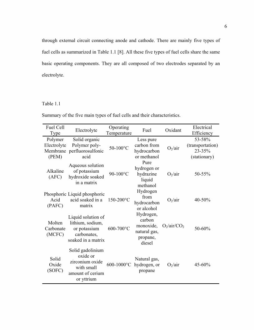
through external circuit connecting anode and cathode. There are mainly five types of
fuel cells as summarized in Table 1.1 [8]. All these five types of fuel cells share the same
basic operating components. They are all composed of two electrodes separated by an
electrolyte.
Table 1.1
Summary of the five main types of fuel cells and their characteristics.
Fuel Cell Type Electrolyte Operating
Temperature Fuel Oxidant Electrical Efficiency
Polymer Electrolyte Membrane
(PEM)
Solid organic Polymer poly-
perfluorosulfonicacid
50-100°C
Less pure carbon from hydrocarbon or methanol
O2/air
53-58% (transportation)
23-35% (stationary)
Alkaline (AFC)
Aqueous solution of potassium
hydroxide soaked in a matrix
90-100°C
Pure hydrogen or hydrazine
liquid methanol
O2/air 50-55%
Phosphoric Acid
(PAFC)
Liquid phosphoric acid soaked in a
matrix 150-200°C
Hydrogen from
hydrocarbon or alcohol
O2/air 40-50%
Molten Carbonate (MCFC)
Liquid solution of lithium, sodium,
or potassium carbonates,
soaked in a matrix
600-700°C
Hydrogen, carbon
monoxide, natural gas,
propane, diesel
O2/air/CO2 50-60%
Solid Oxide
(SOFC)
Solid gadolinium oxide or
zirconium oxide with small
amount of cerium or yttrium
600-1000°CNatural gas, hydrogen, or
propane O2/air 45-60%
7
All these five types of fuel cells share the same basic operating components. They are all
composed of two electrodes separated by an electrolyte. Ions move in from one direction
and this direction depends on the electrolyte. While the electrons flow through an
external circuit connected between the electrodes. Each type of fuel cell is characterized
by the electrolyte. It is generally considered that the two types of fuel cells, the polymer
electrolyte membrane (PEM) and the solid oxide fuel cell, are most likely to succeed in
commercial application.
The most obvious difference between the different types of fuel cell is their operating
temperature. Molten carbonate and solid oxide fuel cells have the highest operating
temperatures of 800–1000 °C compared to the much lower operating temperatures of
around 100 °C for alkaline and PEM fuel cells and around 200 °C for phosphoric acid
fuel cells (PAFC). PEMFCs have low operating temperature and can be used in cars and
portable devices. SOFCs are competitive to other fuel cell types because they are the
most efficient fuel cell type currently under development, they have fuel flexibility, and
cost effective when a certain industrially mature process technology such as thin film
process is applied. They are also quiet systems which can be used as indoor applications.
1.3 Solid Oxide Fuel Cells (SOFCs)
SOFCs can be characterized with its solid ceramic components especially solid
electrolyte which is a composite oxide. SOFCs consist of the cathode where oxygen is
8
reduced to oxygen ions, electrolyte where those oxygen ions pass through toward the
anode, and the anode where the oxygen ions react with fuel. This electrochemical
reaction mechanism inside the fuel cell is shown schematically in Fig. 1.3. The
theoretical maximum efficiency is over 80%. Multiple cells can be connected to produce
larger output power. Conventional SOFCs operate at high temperatures between 800-
1000 °C. This high operating temperature allows internal reforming, promotes rapid
electro catalysis without the need for precious metals such as platinum, and produces
high quality heat which can be used for combined heat processor to increase the
efficiency even further [9]. The hydrocarbon fuel is catalytically converted into carbon
monoxide and hydrogen in the SOFC and then electrochemically reacts to produce CO2
and water at the anode. But there is some draw back in using high temperature
environment. Only a few materials can withstand that high temperature and most of
them are economically not suitable for mass production.
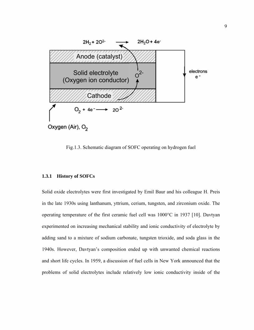
9
Fig.1.3. Schematic diagram of SOFC operating on hydrogen fuel
1.3.1 History of SOFCs
Solid oxide electrolytes were first investigated by Emil Baur and his colleague H. Preis
in the late 1930s using lanthanum, yttrium, cerium, tungsten, and zirconium oxide. The
operating temperature of the first ceramic fuel cell was 1000°C in 1937 [10]. Davtyan
experimented on increasing mechanical stability and ionic conductivity of electrolyte by
adding sand to a mixture of sodium carbonate, tungsten trioxide, and soda glass in the
1940s. However, Davtyan’s composition ended up with unwanted chemical reactions
and short life cycles. In 1959, a discussion of fuel cells in New York announced that the
problems of solid electrolytes include relatively low ionic conductivity inside of the
10
electrolyte, melting, and short-circuiting between electrodes due to conductivity of
electrolyte at high temperature.
More recently, advances in materials technology and climbing energy prices have
opened the possibilities that SOFC can replace some fossil fuel based power generation.
In 1962 researchers at Westinghouse, for example, experimented on cells which are
using zirconium oxide and calcium oxide as electrolyte materials. Another example is a
140 kW peak power SOFC cogeneration system, supplied by Siemens Westinghouse,
which is presently operating in the Netherlands. This system has been operated for over
16,000 hours and becoming the longest running fuel cell in the world [11]. DoE and
Siemens Westinghouse are planning to place a 1 MW fuel cell cogeneration plant in near
future [12].
1.3.2 SOFC Operating Mechanism
SOFCs differ in many respects from other fuel cell technologies. First, they are
composed of all solid-state materials. Second, the normal operating temperature range of
SOFCs is 600-1000°C which is significantly higher than other major types of fuel cells.
Third, because its component materials are all ceramics there is no need for precious
metals. Many different shapes of SOFCs are possible such as tubular, disk, and planar
shapes. Among those different shapes planar shape cells are adopted more recently by
11
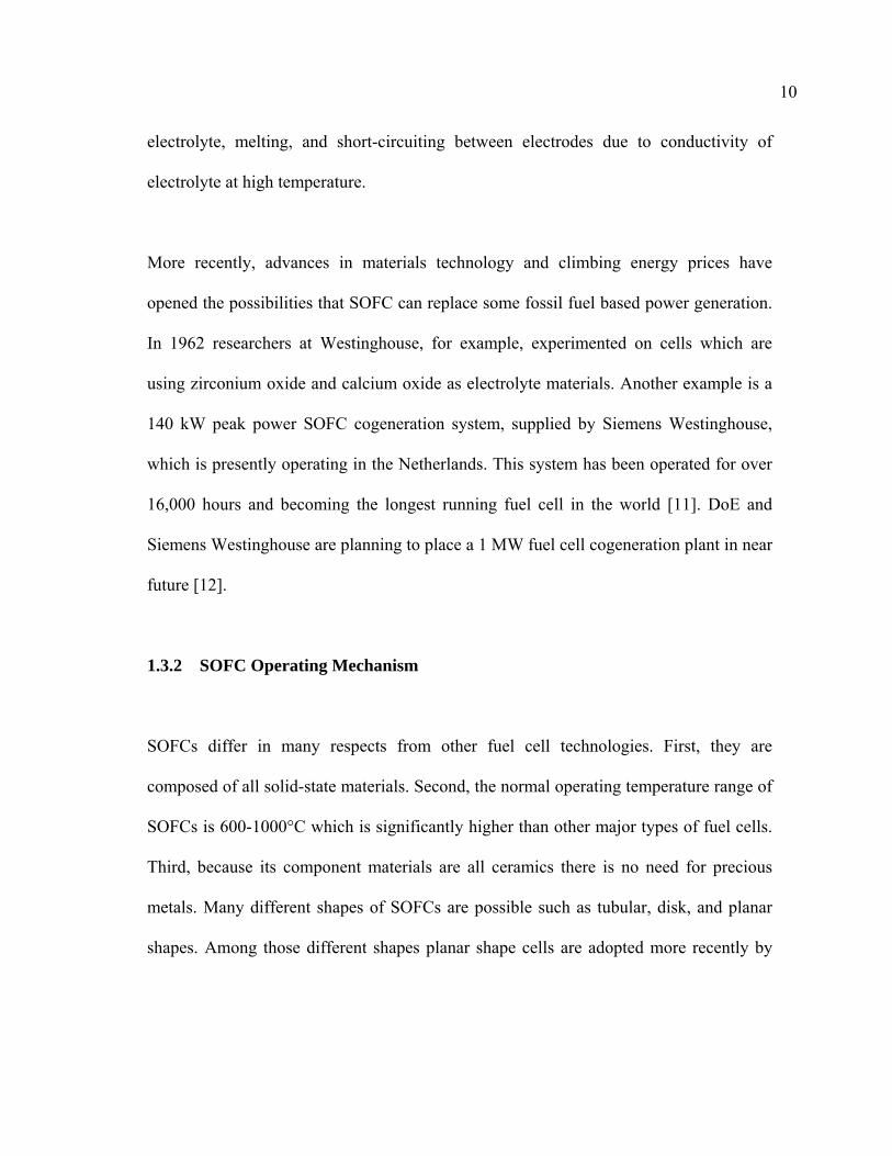
many developers and widely used today by industries. Schematic SOFC operating
mechanism is shown in Fig.1.4.
Fig.1.4. Schematic diagram showing the general operating principles of SOFC
Fuel is supplied to the anode side and oxygen is supplied to the cathode side of the fuel
cell. At the anode surface oxidation of oxygen ions occurs in the process of reaction
between fuel gas and oxygen ions, thereby electrons are released. In this process oxygen
concentration gradient created. This oxygen concentration gradient created across the
electrolyte attracts oxygen ions from the air side to the anode across the electrolyte.
Electrical connection between the cathode and the anode allows electrons to flow from
12
the anode to the cathode and oxygen ion conductions from cathode to anode through
electrolyte maintains overall electrical charge balance. The only byproduct of this
process is a pure water vapor (H2O) and heat in case of hydrogen fuel, as illustrated in
Table 1.2. The SOFC reactions at each electrode are summarized in table 1.2. Unlike
other types of fuel cells moderately high operating temperature eliminates the need for
an expensive external reformer.
Table 1.2
The electrochemical reactions on each electrode in SOFC
Electrode Chemical Reaction
Cathode O2 + 4e- → 2 O2-
Anode
(1) H2 + O2- → H2O + 2e-,
(2) CO + O2- → CO2 + 2e-,
(3) CH4 + 4O2- → 2H2O + CO2 + 8e- (for hydrocarbon fuels)
1.4 Materials for SOFC Components
SOFCs are composed of an anode, a cathode, and a electrolyte. The main function of the
electrodes is working as a reaction site of the reactants (fuel or oxygen) along with the
electrolyte without being consumed or corroded. Electrochemical reaction site is limited
13
only to the triple phase boundary (TPB) where electrode, fuel, and electrolyte come into
contact. Supplied fuel gas disperses through the anode and frees out electrons to the
anode when they meet oxygen ions at the anode side and form water molecules. Oxygen
molecules enter into the cathode side and combine with electrons supplied from anode
side to form oxygen ions then pass across the electrolyte to meet the fuel gas at the
anode side. The electrolyte is where the main power loss of SOFC occurs because of its
low ionic conductivity at low temperature. It also acts as a gas tight membrane which
prevents the fuel gas and oxygen from intermixing. Another important function of
electrolyte is the separation of the two electrodes. If current flows between the two
electrodes through the electrolyte considerable power loss of the fuel cell can happen. It
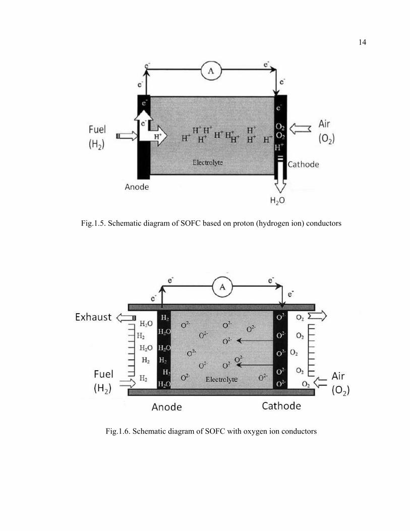
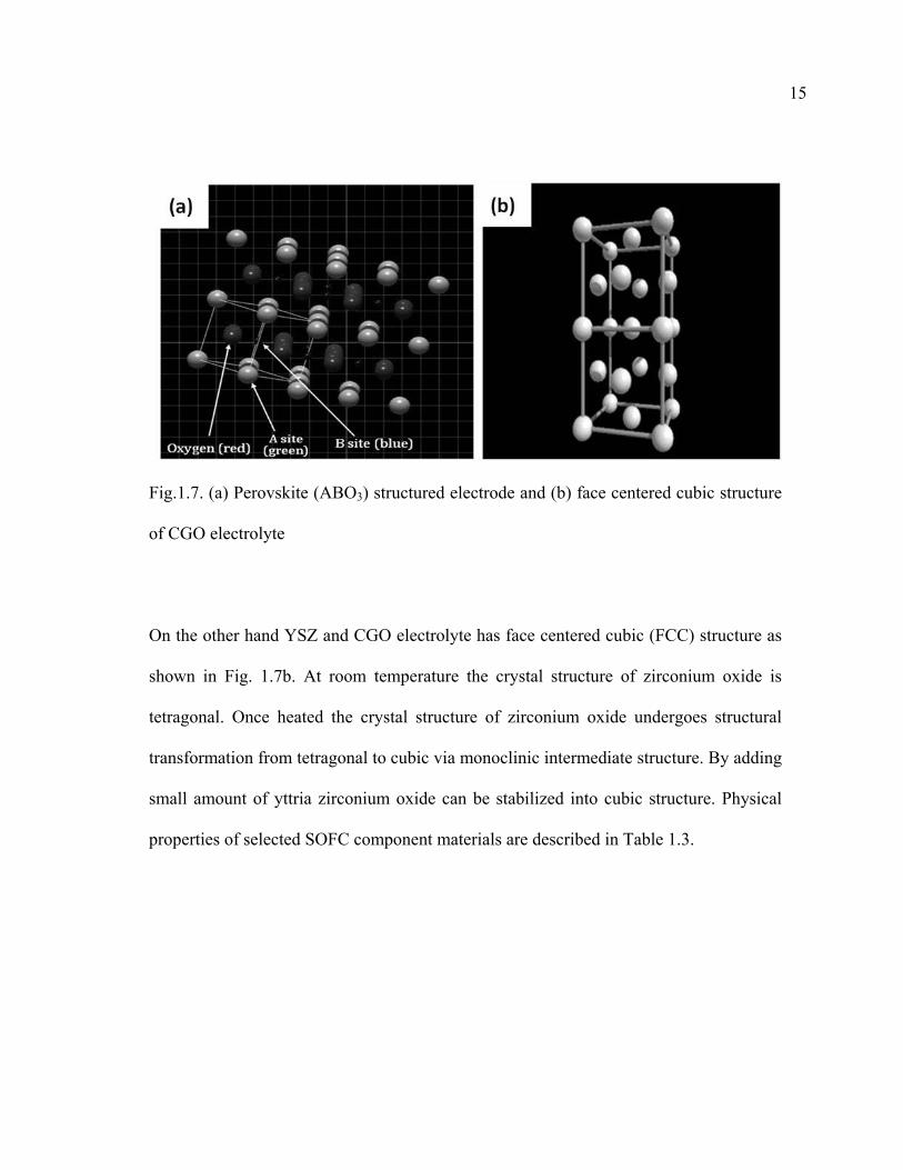
can either be an hydrogen ion conductor or a oxygen ion conductor as shown in Figs. 1.5
and 1.6 respectively.
High operating temperature of the SOFC places strict limitations on its component
materials used as electrolytes, anodes, cathodes, and interconnects. Each component
must meet multiple requirements and must have more than one function. For example,
all components must be chemically stable in reducing and oxidizing conditions as well
as physically stable to avoid cracking or delamination during operation. Currently, the
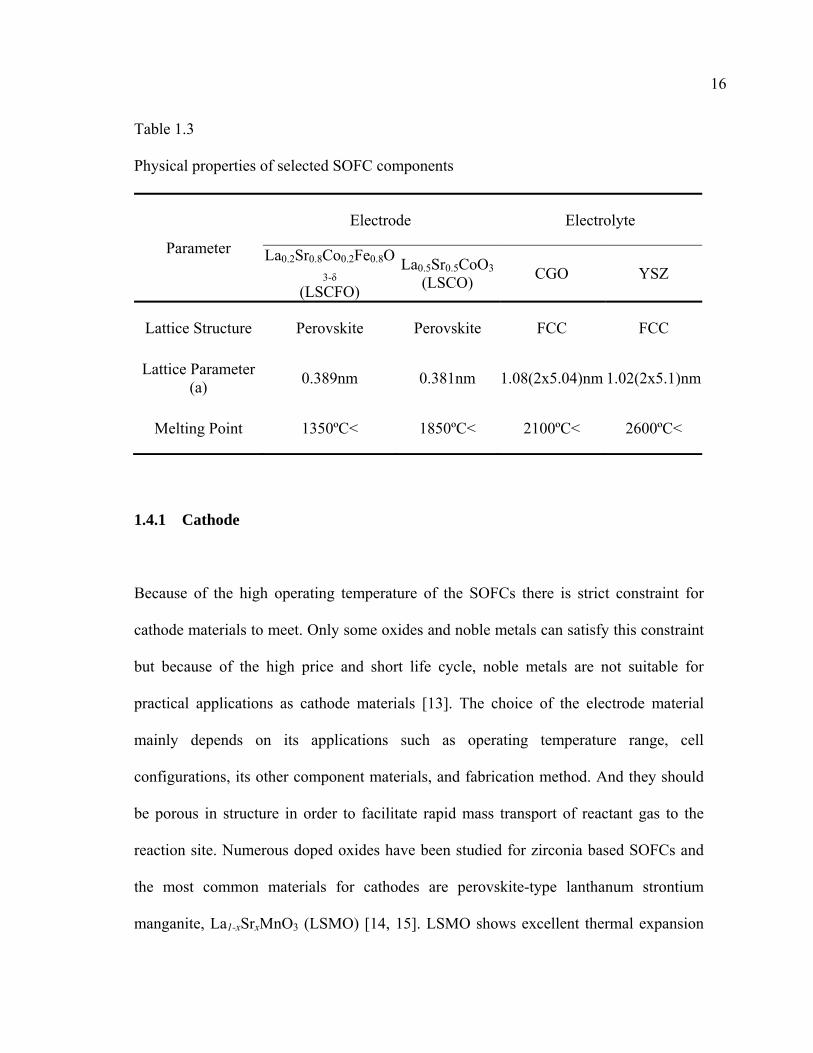
most widely used electrode materials are perovskite type materials where “A” and “B”
sites are doped with divalent cations for increased performance as shown in Fig. 1.7a.
14
Fig.1.5. Schematic diagram of SOFC based on proton (hydrogen ion) conductors
Fig.1.6. Schematic diagram of SOFC with oxygen ion conductors
15
Fig.1.7. (a) Perovskite (ABO3) structured electrode and (b) face centered cubic structure
of CGO electrolyte
On the other hand YSZ and CGO electrolyte has face centered cubic (FCC) structure as
shown in Fig. 1.7b. At room temperature the crystal structure of zirconium oxide is
tetragonal. Once heated the crystal structure of zirconium oxide undergoes structural
transformation from tetragonal to cubic via monoclinic intermediate structure. By adding
small amount of yttria zirconium oxide can be stabilized into cubic structure. Physical
properties of selected SOFC component materials are described in Table 1.3.
16
Table 1.3
Physical properties of selected SOFC components
Parameter
Electrode Electrolyte
La0.2Sr0.8Co0.2Fe0.8O3-δ
(LSCFO)
La0.5Sr0.5CoO3(LSCO) CGO YSZ
Lattice Structure Perovskite Perovskite FCC FCC
Lattice Parameter (a) 0.389nm 0.381nm 1.08(2x5.04)nm 1.02(2x5.1)nm
Melting Point 1350ºC< 1850ºC< 2100ºC< 2600ºC<
1.4.1 Cathode
Because of the high operating temperature of the SOFCs there is strict constraint for
cathode materials to meet. Only some oxides and noble metals can satisfy this constraint
but because of the high price and short life cycle, noble metals are not suitable for
practical applications as cathode materials [13]. The choice of the electrode material
mainly depends on its applications such as operating temperature range, cell
configurations, its other component materials, and fabrication method. And they should
be porous in structure in order to facilitate rapid mass transport of reactant gas to the
reaction site. Numerous doped oxides have been studied for zirconia based SOFCs and
the most common materials for cathodes are perovskite-type lanthanum strontium
manganite, La1-xSrxMnO3 (LSMO) [14, 15]. LSMO shows excellent thermal expansion
17
coefficient match with zirconia electrolytes such as YSZ and provide good performance
in the operating temperatures range of 800-1000°C.
Cation vacancies inside LSMO enable the conductivity of LSMO and this conductivity
can be improved by using lower valence ions as dopants for either the A or B sites. The
alkaline earth metals, magnesium, calcium, and strontium have all been used as dopants,
together with nickel [14, 16]. The conductivity of LSMO varies with strontium content,
with an optimum strontium level. La3+ can be replaced with divalent cations to increase
the electric conductivity through the increased Mn4+ ratio inside and the conduction
happens by small polaron jumping. Although LSMO is an excellent cathode materials
LSMO is not chemically compatible with zirconia electrolyte in high temperature
applications because above 1300 °C manganese can diffuse into the zirconia electrolyte
and diminish the performance both of the cathode and the electrolyte [17].
Doped lanthanum cobaltite, LaCoO3 (LCO) is another promising perovskite material that
has been widely studied and used as a cathode material for SOFCs [14, 18]. LCO also
shows very good p-type conductivity and at high temperatures it shows a large oxygen
deficiency [19]. By doping a divalent cation such as strontium on the La3+ site La1-
xSrxCoO3 (LSCO) the conductivity can be improved [20]. Further improvements in
performance have been found by substituting iron on the cobalt site such as La1-xSrxCo1-
yFeyO3 (LSCFO). LSCO generally shows even higher conductivity than LMO under the
same conditions [17, 18]. For even higher overall fuel cell performance composite
18
electrodes can be used. Composite electrodes consist of electrode and electrolyte
materials. The addition of electrolyte materials to the cathode has improves the
electrochemical performance of the cathode at lower temperature regime by increasing
the effective reaction sites [21].
1.4.2 Anode
Anode side is where reduction of fuel is taking place and because of this condition
metals can be used as anode materials. But the anode metals must be oxidizing resistant
because the composition of the fuel can be changed during the operation. Similar to
cathodes, anodes can also be fabricated as composite mixtures of electrolyte materials
and nickel oxide (NiO) but unlike the electrolyte the anode must have porous structure
and this should be maintained during high temperature operation [21]. Those electrolyte
materials mixed with nickel oxide can inhibit sintering of the nickel particles and can
ease the thermal expansion coefficient mismatch between the anode and the electrolyte.
In addition, the anode must be electrically conducting to be functional as an electrode.
The nickel content in nickel/solid electrolyte cermet decide conductivity of the Ni
cermet anode. The minimum amount of nickel necessary for electrical conductivity is
about 30 vol%. Below this amount the conductivity of the anode is about the same as
that of the solid electrolyte which is electronically not conducting. Above this amout the
conductivity increases by about three orders of magnitude. The conductivity of the anode
19
depends on its microstructure, the size and particle size distribution of the solid
electrolyte and nickel particles, and the inter-connectivity of the nickel particles in the
cermet. The proportion of nickel used in the anode cermet also influences the thermal
expansion mismatch between the solid electrolyte and the anode. As the nickel content
in nickel/yttria stabilized zirconia increases the thermal expansion coefficient of a
nickel/yttria stabilized zirconia cermet increases linearly. This increased thermal
expansion coefficient will cause greater thermal mismatch at the interface of electrolyte
and electrode. This will result in cracking of the electrolyte or delamination of the anode
during the fabrication or thermal cycling.
Because of all these drawbacks of Ni cermet, electrically conducting oxides, which are
stable under both oxidizing and reducing conditions, have been actively studied in recent
years as potential alternative anode materials to nickel [22, 23]. The use of oxide anodes
would solve many problems associated with nickel cermet anodes used in direct
reforming SOFCs such as sulfur poisoning, carbon deposition, and sintering. Nickel
oxide formation also can be avoided. As possible anode materials LaCrO3 (LCO),
strontium titanate, SrTiO3 (STO), doped LCO, and doped STO have been studied. In the
case of LCO calcium (Ca), strontium (Sr) and titanium (Ti) dopants have been used.
From recent studies anodes which are capable of direct hydrocarbon reforming without
the need for any oxidant have been developed [24, 25]. One of these anodes is copper-
based anode.
20
There is currently much interest in developing alternative anode materials to the
nickel/YSZ cermet. Nickel-ceria cermet anodes is being studied by many researchers for
gadolinia doped ceria based SOFCs as well as for zirconia based SOFCs. Nickel/ceria
cermet anodes have been shown to give sufficiently good performance in especially
ceria based SOFCs operating at temperatures around 500 °C. Ceria has also been added
to nickel/YSZ anodes to improve both the electrical performance and the resistance to
carbon deposition.
1.4.3 Electrolyte
Major power loss and efficiency degradation of SOFC is closely related to electrolyte
characteristics and the operating temperature is strongly depends on the ionic
conductivity and the thickness of the electrolyte layer. There are two possible
approaches to these problems. Finding alternate electrolyte materials which have higher
ionic conductivity is one solution and the other one would be decreasing electrolyte
thickness. To decrease the electrolyte layer thickness some of the current SOFCs
adopted electrode supporting configuration. In this case the minimum dense electrolyte
thickness that can be produced reliably is 10 to 15µm and the typical thickness is 30 µm.
Current technology employs yttria stabilized zirconia (Y2O3 stabilized ZrO2 or YSZ,
(ZrO2)0.92(Y2O3)0.08) as solid electrolyte materials because of its low material cost, high
temperature stability and moderately high oxygen ion conductivity from intermediate to
21
high temperature regime. YSZ shows pure oxygen ion conduction with no electrical
conductivity. The ZrO2 crystal structure includes two oxide ions for every zirconium ion
but in Y2O3 crystal structure there are only 1.5 oxide ions to every yttrium ion. This
results in vacancies in the crystal structure where oxide ions are missing. Using these
vacancies oxide ions generated from the TPB at the cathode side can pass through
electrolyte to reach the anode side. The most commonly used zirconia stabilizing
dopants are Y2O3, Sc2O3, CaO, MgO, and certain rare earth oxides such as Nd2O3,
Sm2O3. But despite of its relatively high oxygen ion conductivity it is not suitable for
low temperature applications below 600°C furthermore it shows interface diffusion and
second phase formation problem after some cycles. Gadolinia-doped ceria (CGO)
exhibits superb performance in low temperature regime (400-600°C). However in a
reducing high temperature environment in anode ceria undergoes partial reduction. This
reduction leads to electronic conduction between anode and cathode and significantly
lowers the efficiency of the SOFC. It can also bring an undesirable structural change at
the interface. Other oxide based ceramic electrolytes candidates which can replace CGO
for even low temperature operation are samarium doped cerium oxide
(Ce0.85Sm0.15)O1.925 (SDC), and Calcium doped cerium (Ce0.88Ca0.12)O1.88 (CDC)[26].
1.5 SOFC Cell Configurations
Many different kinds of SOFC configurations have been adapted to increase power
output and efficiency. The maximum voltage output a single cell can generate is 0.5 to
22
0.9 volts of DC electricity with maximum efficiency of 60% since they are small in size
and considerable ohmic loss occurs inside of the cell. To address maximum power
output stacked cell configuration has been used. There are two major types in SOFC, a
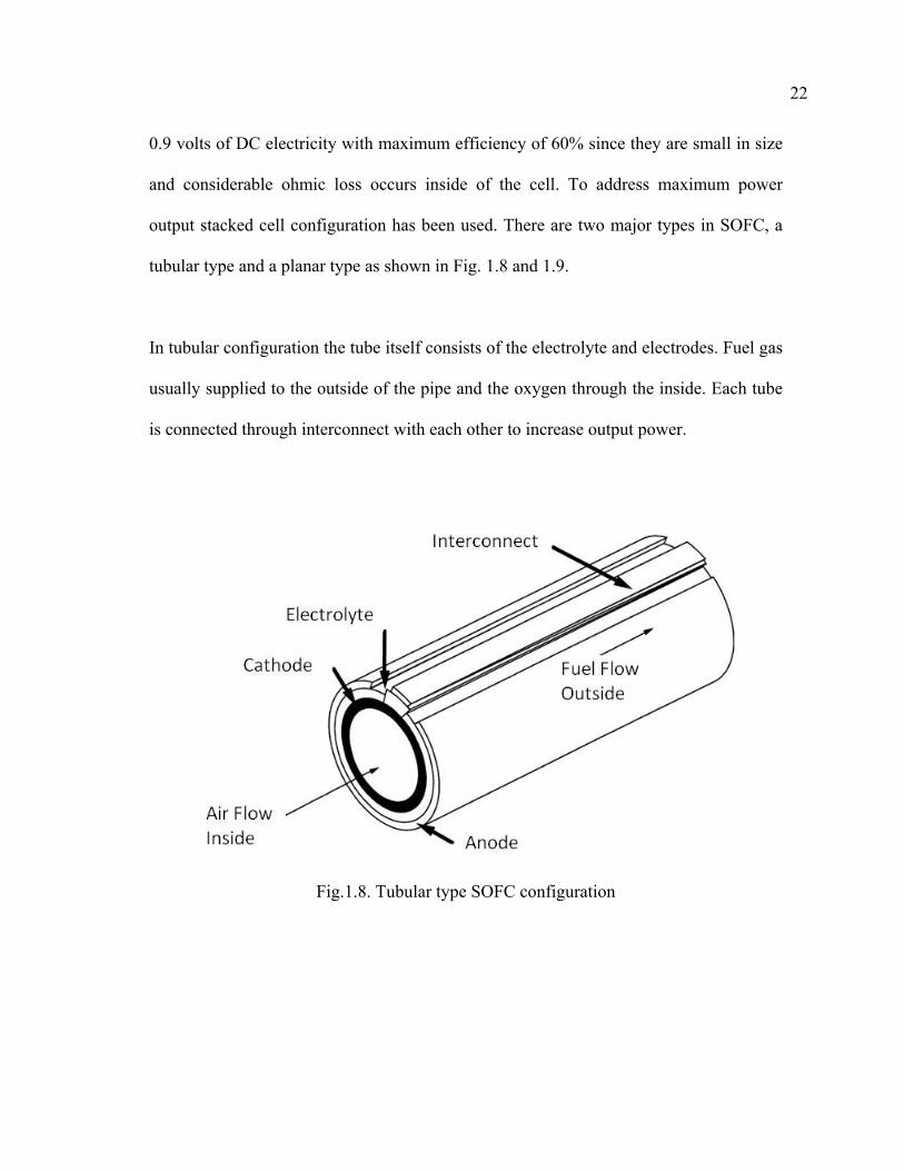
tubular type and a planar type as shown in Fig. 1.8 and 1.9.
In tubular configuration the tube itself consists of the electrolyte and electrodes. Fuel gas
usually supplied to the outside of the pipe and the oxygen through the inside. Each tube
is connected through interconnect with each other to increase output power.
Fig.1.8. Tubular type SOFC configuration
23
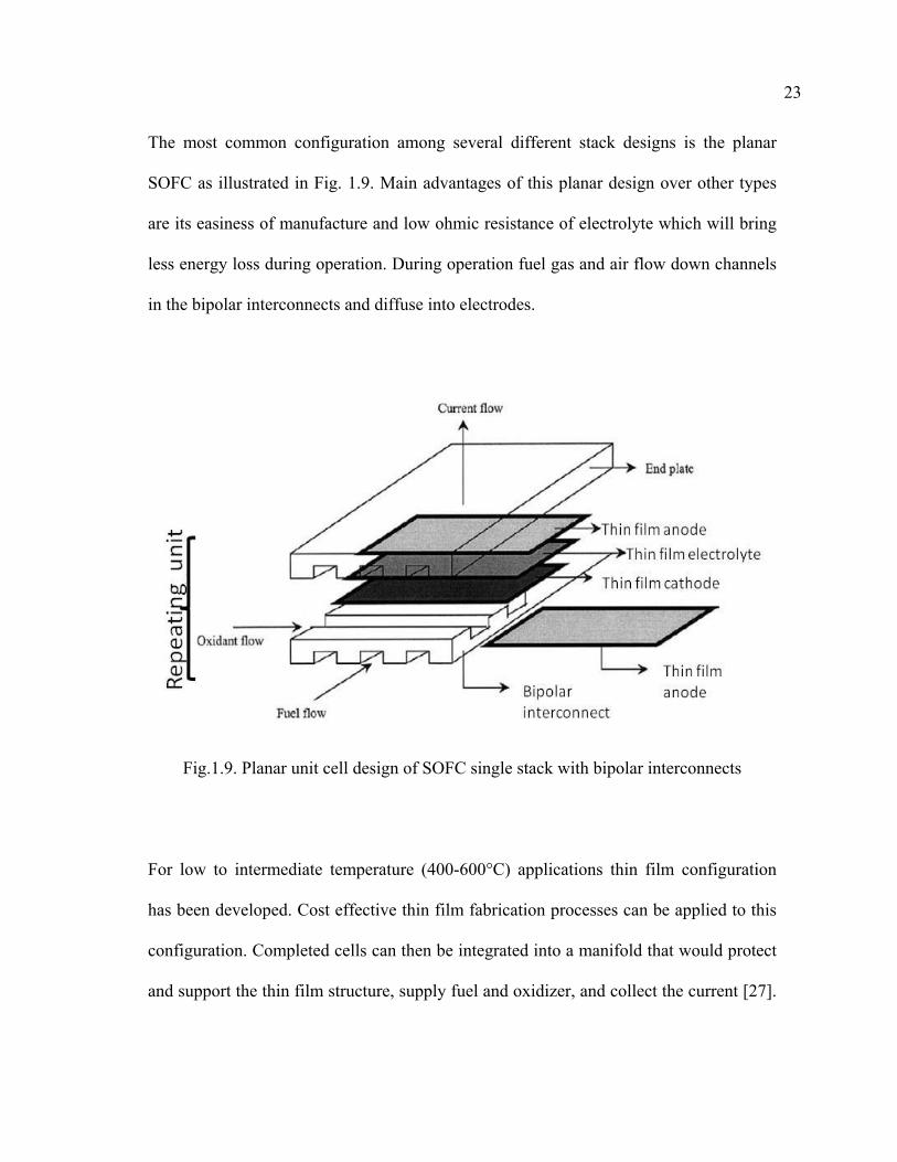
The most common configuration among several different stack designs is the planar
SOFC as illustrated in Fig. 1.9. Main advantages of this planar design over other types
are its easiness of manufacture and low ohmic resistance of electrolyte which will bring
less energy loss during operation. During operation fuel gas and air flow down channels
in the bipolar interconnects and diffuse into electrodes.
Fig.1.9. Planar unit cell design of SOFC single stack with bipolar interconnects
For low to intermediate temperature (400-600°C) applications thin film configuration
has been developed. Cost effective thin film fabrication processes can be applied to this
configuration. Completed cells can then be integrated into a manifold that would protect
and support the thin film structure, supply fuel and oxidizer, and collect the current [27].
24
To produce desired amounts of power output, single cell elements are assembled into a
stack. Stack is a basic building block of the fuel cell power plant in which all the cell
components are stacked with interconnecting plates between them. Interconnects are
generally made of doped lanthanum chromate LaCrO3, particularly suitable from its high
electronic conductivity, its stability in the fuel cell environment and its compatibility
with other cell components. Interconnects are shaped to allow flow of the hydrogen and
oxygen to the repeating unit. Early SOFCs used doped CoCr2O4 as interconnect material
[28]. Recently, YCrO3 compound, having great stability in the fuel cell environment, has
been evaluated as an alternative material to LaCrO3 [29]. However, all these materials
are not cost effective. The main problem for using low cost interconnect material, such
as high temperature alloys are a thermal expansion mismatch with other SOFC
components, cost, and long term instability during cell lifetime. Various efforts have
been made to reduce SOFC operating temperature so that low cost materials can be used
along with flexible cell design. Lowering cell operating temperature can bring many
advantages other than cost. At low operating temperature thermal stress between
electrodes and electrolyte due to different thermal expansion coefficient can be greatly
relieved. The cells are connected in electrical series to build a desired output voltage and
can be configured in many different forms depending on their applications. The total
voltage is determined by the number of cells in a stack and the surface area determines
the total current.
25
1.6 SOFC Limitations and Thin Film Approach
Due to high operating temperature the only performance issues related to SOFCs are
ohmic losses during charge transfer process across components and between component
interfaces [30]. Around 1000°C SOFCs are the most fuel-efficient energy sources but
this high temperature place constraints on selecting fuel cell materials and this increases
cost. Moreover this high operating temperature decreases the cell lifetime significantly
due to high thermal stress. High operating temperature also means longer start up time.
For these constraints lowering operating temperature is the best solution to ensure
structural integrity of SOFC, expand life time, and reduce cost since in reduced
temperature environment cheaper interconnect, gasket, and cell component materials can
be utilized.
For many years researchers have been working on reducing this high operating
temperature of SOFCs without diminishing performance. Since the cell performance is
very sensitive to operating temperature 10% drop in temperature will bring 12% drop in
overall performance, due to the increase in internal resistance to the oxygen ion
conduction [31]. Replacing cell component materials with good ionic conductivity at
low temperature has been a solution to this problem. Recently researchers are focusing
on reducing resistance and increasing ionic conductivity of electrolyte by applying thin
film technology. Thin film process is a mature, proven, and cost effective technology.
Thin film SOFC also has other benefits in miniaturization and stacking than easiness of
26
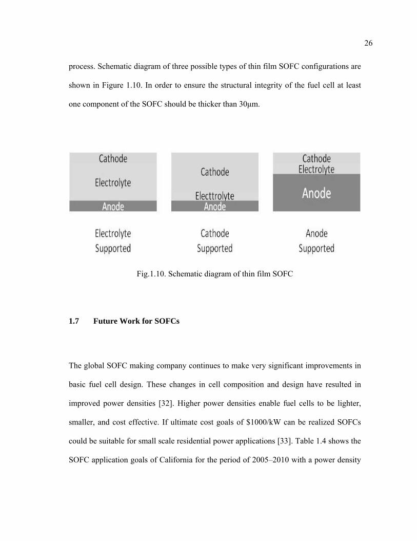
process. Schematic diagram of three possible types of thin film SOFC configurations are
shown in Figure 1.10. In order to ensure the structural integrity of the fuel cell at least
one component of the SOFC should be thicker than 30μm.
Fig.1.10. Schematic diagram of thin film SOFC
1.7 Future Work for SOFCs
The global SOFC making company continues to make very significant improvements in
basic fuel cell design. These changes in cell composition and design have resulted in
improved power densities [32]. Higher power densities enable fuel cells to be lighter,
smaller, and cost effective. If ultimate cost goals of $1000/kW can be realized SOFCs
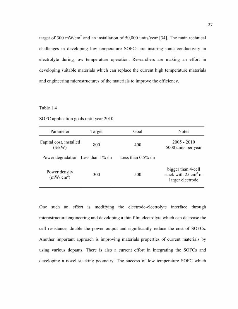
could be suitable for small scale residential power applications [33]. Table 1.4 shows the
SOFC application goals of California for the period of 2005–2010 with a power density
27
target of 300 mW/cm2 and an installation of 50,000 units/year [34]. The main technical
challenges in developing low temperature SOFCs are insuring ionic conductivity in
electrolyte during low temperature operation. Researchers are making an effort in
developing suitable materials which can replace the current high temperature materials
and engineering microstructures of the materials to improve the efficiency.
Table 1.4
SOFC application goals until year 2010
Parameter Target Goal Notes
Capital cost, installed ($/kW) 800 400 2005 - 2010
5000 units per year
Power degradation Less than 1% /hr Less than 0.5% /hr
Power density (mW/ cm2) 300 500
bigger than 4-cell stack with 25 cm2 or
larger electrode
One such an effort is modifying the electrode-electrolyte interface through
microstructure engineering and developing a thin film electrolyte which can decrease the
cell resistance, double the power output and significantly reduce the cost of SOFCs.
Another important approach is improving materials properties of current materials by
using various dopants. There is also a current effort in integrating the SOFCs and
developing a novel stacking geometry. The success of low temperature SOFC which
28
operates directly on hydrocarbon fuel can open an important new opportunity for making
simple, cost-effective power plants [35].
1.8 Summary
Constantly growing world population strongly demands alternate energy sources. SOFCs
appear to be one of the most promising energy sources for the future because of their
high efficiencies and fuel flexibility. Their efficiency and performance has been proven
by successful operation throughout the world. Efficiencies of over 70% are possible
these days if they are combined with heat processors.
Despite the fact that SOFC is the ideal energy source for the future, its high operating
temperature delays its technological advances. Profound efforts have been made in
reducing temperature and this will lead to reduce cell resistance and regain power loss at
low temperature regime. One of such efforts are finding alternate materials such as
gadolinia-doped ceria (CGO) or lanthanum gallate based structures for low temperature
cell components and applying the current thin film technology to reduce electrolyte
resistance such as ultra-thin dense, impermeable CGO electrolyte films. SOFC operating
temperature can be lowered greatly by reducing electrolyte thickness since thin film
electrolyte can perform well even at low temperature because of its increased ionic
conductivity in thin film electrolyte and this will result in many other benefits such as
longer cell life time and shorter start up time. Other benefits from using thin film

29
components can be found in cell design and configuration. Cell stacking is easier with
thin film SOFC components and cell miniaturization is possible for the use of mobile
applications.
30
CHAPTER II
RESEARCH METHODOLOGY
2.1 Pulsed Laser Deposition (PLD) Technique
Because of its narrow frequency bandwidth, coherence and high power density laser is
used in many scientific research works and experiments especially in material processing.
The laser beam is intense enough to vaporize the hardest and most heat resistant
materials. Its high precision, reliability and spatial resolution enabled laser to be used
widely in material processing industry. Thin film processing and micro patterning is
some of the examples [36,37]. Apart from these, complex materials can be deposited
onto desired substrates maintaining its original stoichiometric compositions of the target.
This procedure is called Pulsed Laser Deposition (PLD).
In general, the method of pulsed laser deposition is simple in its procedure. Only limited
numbers of parameters need to be controlled during the process. PLD utilizes small
targets compared with other targets used in other thin film deposition techniques. By
controlling the number of pulses and targets, a fine control of film thickness and multi
layer film can be achieved. Thus a fast prototyping a new material system is a unique
feature of PLD among other deposition methods. The most important feature of PLD is
that the stoichiometry of the target can be reproduced in the deposited films. This is the
result of non equilibrium process originated from an extremely high heating rate of the
31
target surface (108 K/s) due to high energy pulsed laser irradiation. It leads to the
harmonious evaporation of the target compounds. And because of the high heating rate
epitaxial film growth using PLD requires a much lower temperature than other
mentioned film growth techniques [38].
In spite of mentioned advantages of PLD there are some drawbacks in using PLD
technique. One of the major problems is the particulates deposition on the film. This
happens because of surface boiling, expulsion of the liquid layer by shock wave recoil
pressure and exfoliation. Such particulates will greatly affect the growth of the
subsequent layers as well as the electrical properties of the film and should be eliminated
[39]. Another problem is the substrate surface coverage of the plum which is generated
by the adiabatic expansion of laser produced plasma. These features limit the use of PLD
in mass production. Recently new techniques such as inserting a shadow mask to block
the particulates and rotating both target and substrate in order to produce a larger
uniform film, have been developed to overcome the PLD problems mentioned earlier.
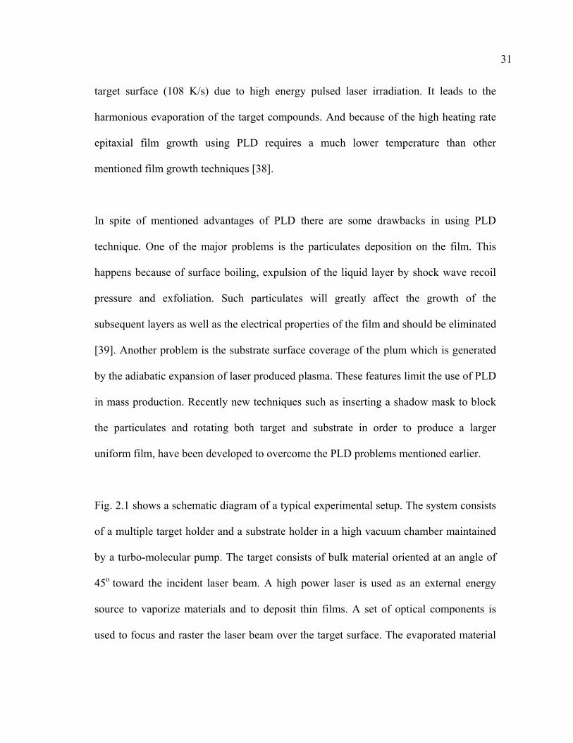
Fig. 2.1 shows a schematic diagram of a typical experimental setup. The system consists
of a multiple target holder and a substrate holder in a high vacuum chamber maintained
by a turbo-molecular pump. The target consists of bulk material oriented at an angle of
45o toward the incident laser beam. A high power laser is used as an external energy
source to vaporize materials and to deposit thin films. A set of optical components is
used to focus and raster the laser beam over the target surface. The evaporated material
32
is deposited onto a substrate facing target separated by the distance of 3 to 5cm. The
substrate temperature can be varied from room temperature to 800oC. The film
microstructure depends on various parameters such as substrate temperature, laser
energy density, pulse repetition rate, pressure inside the chamber, and substrate to target
distance. The separation of the vacuum hardware and the evaporation method makes this
technique so flexible that it can be easily adaptable to different operational modes
without difficulties unlike the system with internally powered evaporation sources. Film
growth can be carried out in a reactive environment containing any kind of gas with or
without plasma excitation. It can also be operated in conjunction with other types of
evaporation sources in a hybrid approach [40].
Fig.2.1. Schematic diagram of the pulsed laser deposition system
33
In contrast to the simple hardware set up, the laser-target interaction is a very complex
physical phenomenon and it includes both equilibrium and nonequilibrium processes.
The mechanism that leads to material ablation depends on laser characteristics, as well
as the optical, topological, and thermodynamic property of target. When the laser energy
is absorbed by a target surface, electromagnetic energy is converted first into electronic
excitation and then into thermal, chemical, and even mechanical energy to cause
evaporation, ablation, excitation, plasma formation, and exfoliation. Evaporations results
in a ‘plume’ consisting of a mixture of energetic species including atoms, molecules,
electrons, ions, clusters, micron sized solid particulates, and molten globules. Inside the
dense plume the collision mean free path is very short. As a result, immediately after the
laser irradiation, the plume rapidly expands into the vacuum from the target surface to
form a nozzle jet with hydrodynamic flow characteristics. With the proper choice of the
laser PLD can be used to grow thin film of any kind of material.
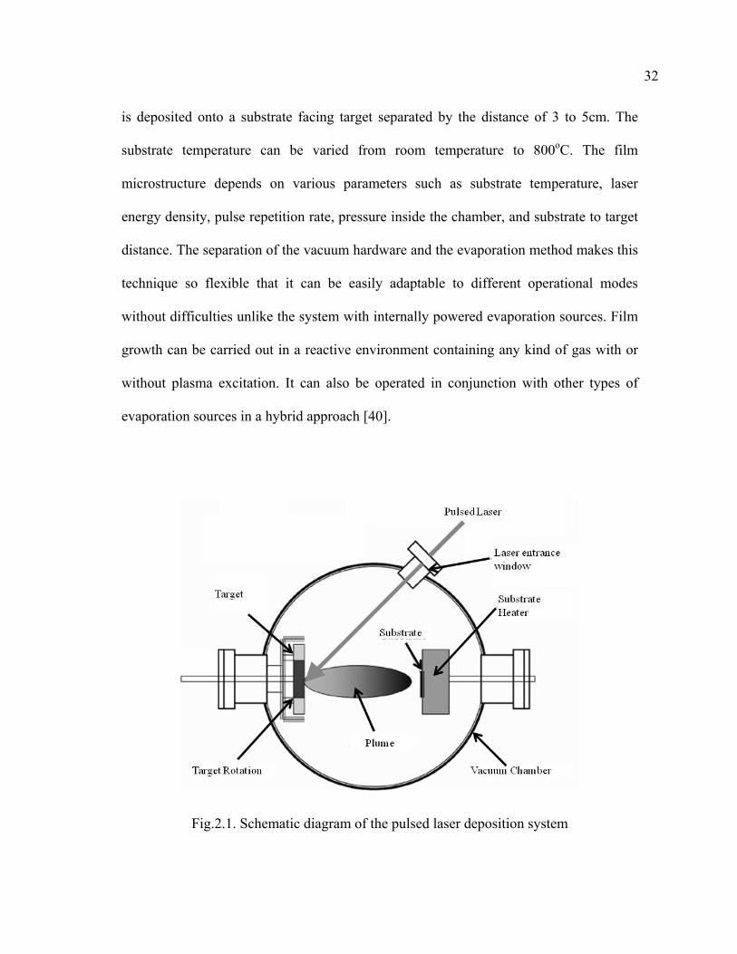
Each of the nanosecond laser pulse and target interaction can be divided into three stages
as shown schematically in figure 2.2. Depending on the type of interaction of the laser
beam with the target laser-target interactions can be categorized into three different
regimes. First, interactions of the laser beam with the target materials which results in
evaporation of the surface layers. Second, interaction of the evaporated material with the
incident laser beam resulting in isothermal plasma formation and expansion, and the
third, anisotropic adiabatic expansion of the plasma and subsequent deposition. The first
34
two interactions start with the laser pulse and continue through out the laser pulse
duration. The third regime starts after the termination of the laser pulse [41].
Fig.2.2. Schematic representation of the stages of laser target interactions during short
pulse high power laser interaction with a solid [41]
2.1.1 Interaction of the Laser Beam with the Target
Surface layers exposed to intense heat of the high power nanosecond laser pulses results
in melting and evaporation of the. Laser parameters such as pulse energy density (E),
pulse duration (t), wavelength (λ) and shape of the laser pulse and materials properties
such as reflectivity, absorption coefficient, heat capacity, density, thermal conductivity
decide the heating rate, melting and evaporation of the target material during pulsed
35
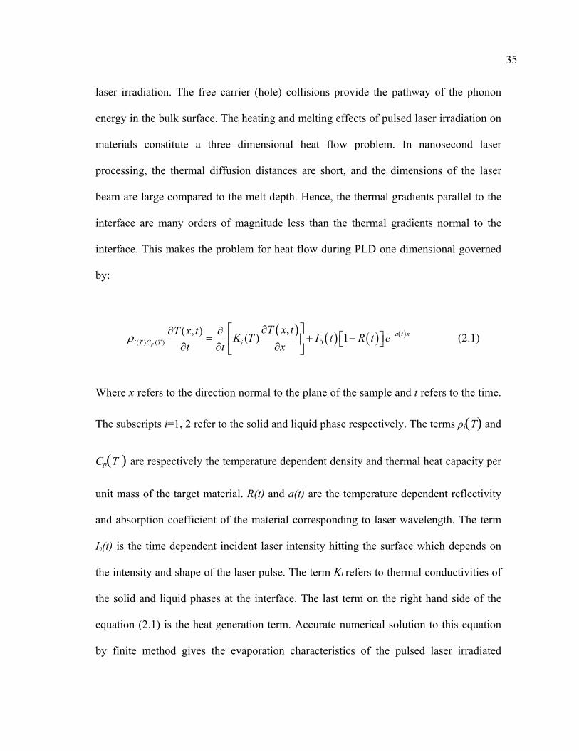
laser irradiation. The free carrier (hole) collisions provide the pathway of the phonon
energy in the bulk surface. The heating and melting effects of pulsed laser irradiation on
materials constitute a three dimensional heat flow problem. In nanosecond laser
processing, the thermal diffusion distances are short, and the dimensions of the laser
beam are large compared to the melt depth. Hence, the thermal gradients parallel to the
interface are many orders of magnitude less than the thermal gradients normal to the
interface. This makes the problem for heat flow during PLD one dimensional governed
by:
( ) ( ) ( ) ( )( ) ( ) 0
,( , ) ( ) 1P
a t xi T C T i
T x tT x t K T I t R t et t x
ρ −⎡ ⎤∂∂ ∂ ⎡ ⎤= + −⎢ ⎥ ⎣ ⎦∂ ∂ ∂⎣ ⎦ (2.1)
Where x refers to the direction normal to the plane of the sample and t refers to the time.
The subscripts i=1, 2 refer to the solid and liquid phase respectively. The terms ρi(T) and
Cp(T ) are respectively the temperature dependent density and thermal heat capacity per
unit mass of the target material. R(t) and a(t) are the temperature dependent reflectivity
and absorption coefficient of the material corresponding to laser wavelength. The term
I0(t) is the time dependent incident laser intensity hitting the surface which depends on
the intensity and shape of the laser pulse. The term Ki refers to thermal conductivities of
the solid and liquid phases at the interface. The last term on the right hand side of the
equation (2.1) is the heat generation term. Accurate numerical solution to this equation
by finite method gives the evaporation characteristics of the pulsed laser irradiated
36
materials. Using this method, the thermal histories of the laser irradiated materials can be
predicted. Thus the effects of the variations in the pulse energy density E, pulse duration
t, and substrate temperature T on the maximum melt depths, solidification velocities and
surface temperatures can be computed. Although the presence of a moving surface
formed as a result of melting or evaporation, and time-dependent optical and material
properties make the analytical solution difficult, simple energy balance considerations
can be taken into account to assess the effects of interaction of the laser irradiation with
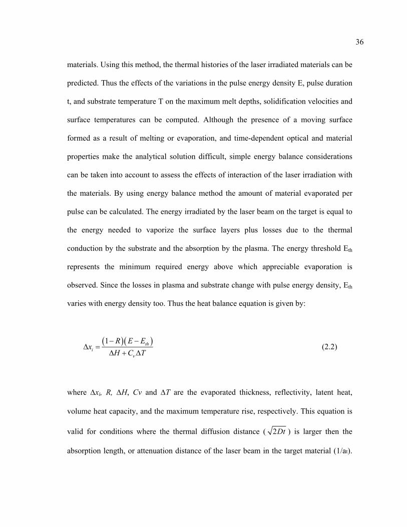
the materials. By using energy balance method the amount of material evaporated per
pulse can be calculated. The energy irradiated by the laser beam on the target is equal to
the energy needed to vaporize the surface layers plus losses due to the thermal
conduction by the substrate and the absorption by the plasma. The energy threshold Eth
represents the minimum required energy above which appreciable evaporation is
observed. Since the losses in plasma and substrate change with pulse energy density, Eth
varies with energy density too. Thus the heat balance equation is given by:
)( )(1i
thR E Ex
H Cν
− −Δ =
Δ + ΔT (2.2)
where Δxi, R, ΔH, Cv and ΔT are the evaporated thickness, reflectivity, latent heat,
volume heat capacity, and the maximum temperature rise, respectively. This equation is
valid for conditions where the thermal diffusion distance ( 2Dt ) is larger then the
absorption length, or attenuation distance of the laser beam in the target material (1/at).
37
In the above expression, D is the thermal diffusivity of the target, and t is the laser pulse
duration. In equation (2.2) the energy threshold depends on laser wavelength, pulse
duration, plasma losses, and the thermal and optical properties of the material.
2.1.2 Interaction of the Laser Beam with Evaporated Materials
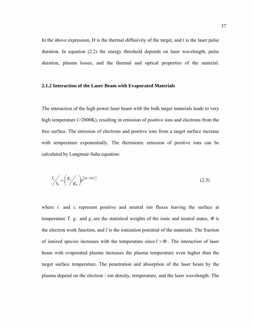
The interaction of the high power laser beam with the bulk target materials leads to very
high temperature (>2000K), resulting in emission of positive ions and electrons from the
free surface. The emission of electrons and positive ions from a target surface increase
with temperature exponentially. The thermionic emission of positive ions can be
calculated by Langmuir-Saha equation:
( )
0 0
I kTi g ei gφ⎡ − ⎤⎣ ⎦+ +⎛ ⎞= ⎜ ⎟
⎝ ⎠ (2.3)
where i+ and i0 represent positive and neutral ion fluxes leaving the surface at
temperature T. g + and g 0 are the statistical weights of the ionic and neutral states, Φ is
the electron work function, and I is the ionization potential of the materials. The fraction
of ionized species increases with the temperature since I > Φ . The interaction of laser
beam with evaporated plasma increases the plasma temperature even higher than the
target surface temperature. The penetration and absorption of the laser beam by the
plasma depend on the electron / ion density, temperature, and the laser wavelength. The
38
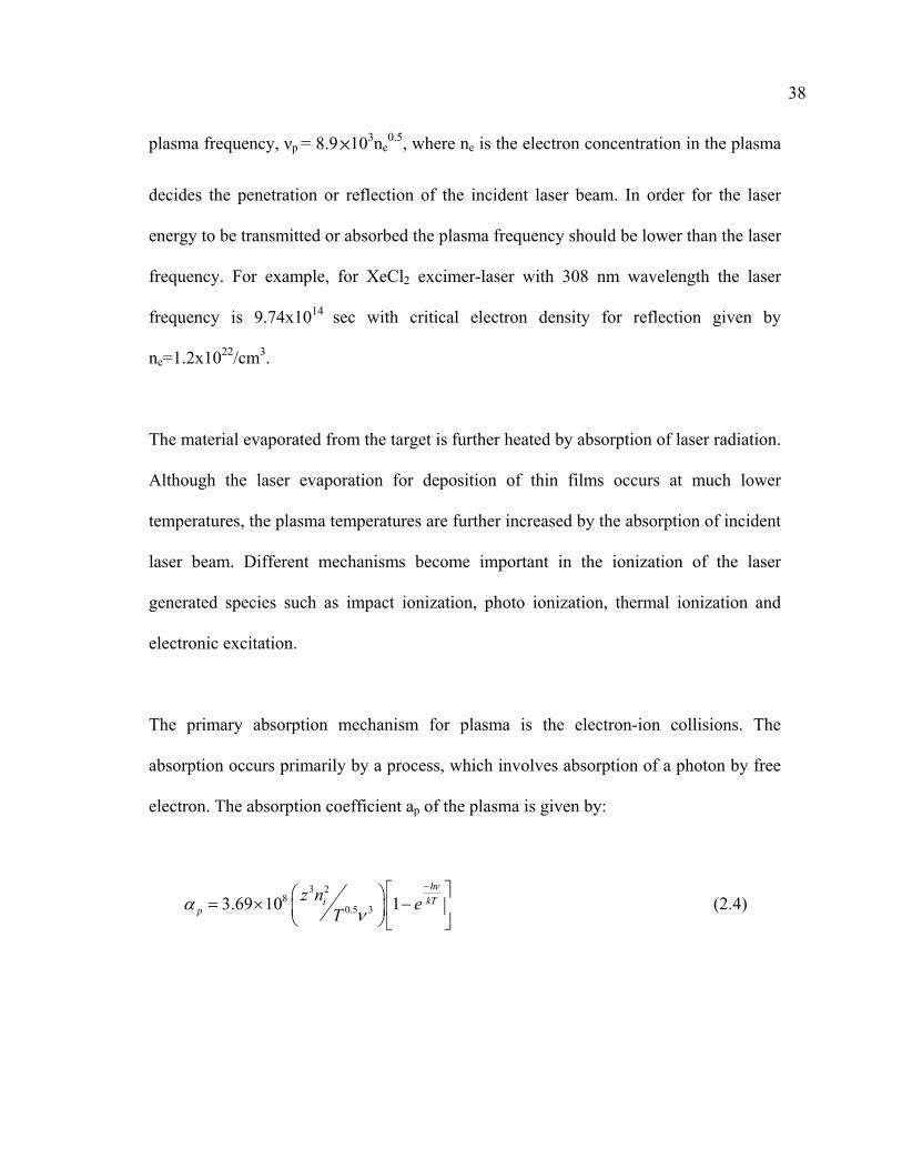
plasma frequency, νp = 8.9 103ne0.5, where ne is the electron concentration in the plasma
decides the penetration lection of the incident laser beam. In order for the laser
energy to be transmitted or absorbed the plasma frequency should be lower than the laser
frequency. For exam 2 excimer-laser with 308 nm wavelength the laser
frequency is 9.74x10¹⁴ with critical electron density for reflection given by
ne=1.2x10²²/cm3.
The material evaporated from the target is further heated by absorption of laser radiation.
Although the laser evaporation for deposition of thin films occurs at much lower
temperatures, the plasma temperatures are further increased by the absorption of incident
laser beam. Different mechanisms become important in the ionization of the laser
generated species such as impact ionization, photo ionization, thermal ionization and
electronic excitation.
The primary absorption echanism for plasma is the electron-ion collisions. The
absorption occurs primarily by a process, which involves absorption of a photon by free
electron. The absorption coefficient ap of the plasma is given by:
or ref
ple, for XeCl
sec
m
3 28
0.5 33.69 10 1h
kTip
z n eT
ν
α ν
−⎡ ⎤⎛ ⎞= × −⎢ ⎥⎜ ⎟⎝ ⎠ ⎣ ⎦
(2.4)
39
where Z, ni, and T are the average charge, ion density, and temperature of the plasma,
reflectively, and h, k, and v are the Plank constant, Boltzmann constant, and frequency
of the laser light respectively. The term 1 hekT
ν−⎡ ⎤−⎢ ⎥⎣ ⎦in equation (2.4) represents the
losses due to stimulated emission. For KrF excimer laser (λ=248nm), the exponential
term becomes unity for T<<40,000K and can be approximately by hv/kT for
T>>40,000K. The absorption term shows a T0.5 dependence for low temperature
(T<<40,000K for λ=248nm, T<<40,000K for λ=1.06nm) and T1.5 for high temperatures.
As it is seen, the heating of the evaporated materials depends on the concentration of the
ionized species, plasma temperature, wavelength, plasma temperature, wavelength, pulse
duration, etc.. Also the particle density in the plasma depends on the degree of ionization,
evaporation rate, and the plasma expansion velocities. Because of the high expansion
velocities of the leading plasma edge, the electron and ion densities decrease very
rapidly with time. This makes the plasma transparent to the laser beam for larger
distances away from the target surface. The inner edge of the plasma in a thin region
close to the surface of the target it constantly absorbing laser radiation due to the
constant augmentation of the plasma with evaporated particles. A schematic diagram of
the laser interaction with the plasma target is shown in figure 2.3.
40
Fig.2.3. Schematic diagram representing the different phases present during irradiation
of a laser on a bulk target: (A) unaffected bulk target, (B) evaporated target materials,
(C) dense plasma absorbing the laser radiation, and (D) expanding plasma transparent to
the laser beam [41]
The diagram shows four separate regions which can be distinguished during the laser
pulse. Those are unaffected bulk target, evaporating target surface, area near the surface
of the target absorbing the laser beam, and rapidly expanding outer edge which is
transparent to the laser beam. A dynamic equilibrium exists between the plasma
absorption and the rapid transfer of thermal energy into kinetic energy. These are two
mechanisms controlling the isothermal temperature of the plasma. The initial dimensions
of the plasma are in the millimeter range in the transverse direction, while they are less
than 1μm in the perpendicular direction. In the isothermal regime and assuming an initial
expansion velocity of 105-106 cm/sec, the perpendicular dimension of the plasma is in
the order of 10 to 100μm at the end of a 30 nsec laser pulse. The large density gradients
41
cause the rapid plasma expansion in vacuum. The plasma absorbing the laser energy can
be simulated as a HT-HP gas which is initially confined in small dimensions and is
suddenly allowed to expand in a vacuum. The gas dynamic equations governing the
expansion of the plasma consist of the equation of continuity and the equation of motion.
The velocity, density, and the pressure profiles in the plasma are shown schematically in
figure 2.4. It shows that the density is maximum while the velocity is minimum at the
inner edge of the plasma. The plasma density and the pressure gradients decreases non
linealy from the surface of the target while the velocity increases linearly. In the initial
stages of expansion the acceleration is very high when the expansion velocities are low.
When the expansion velocities increase, the acceleration starts to decrease and ultimately
becomes zero, resulting in the elongated plasma shape.
Fig.2.4. Schematic profile showing the density (n), pressure (P), and velocity (v)
gradients in the plasma in x direction, normal to the target surface. [41]
42
2.1.3 Adiabatic Plasma Expansion and Film Deposition
After the termination of the laser pulse in vacuum there is no additional input of particles
from the target into the plasma because there is no absorption of laser energy. Thus an
adiabatic expansion occurs with a thermodynamic relation given by:
(2.5)
where the γ corresponds to the ratio of the specific heat capacities at constant pressure
Cp and volume Cv. In the adiabatic regime, the thermal energy is converted to kinetic
energy while the plasma achieving extremely high expansion velocities. The temperature
drop is slow because the cooling caused by expansion is balanced by energy regained
from recombination processes by ions and the plasma expands in one direction. The
initial dimensions of the plasma are much larger in the transverse directions (y and z)
which are in the order of millimeter, while in perpendicular direction (x) is in the order
of 20-100μm. In the adiabatic expansion regime the velocity of the plasma increases in
the direction of the smallest dimension.
( ) ( ) ( ) 1T X t Y t Z t consγ −⎡ ⎤ =⎣ ⎦ t
43
2.2 Characterization Methods of Thin Films
Thin film properties are determined by their chemical composition, the content and type
of impurities in the thin film or on the surface, crystal structure of the thin film and on
the surface, and the types and density of structural defects. In addition, as the
applications of thin films extend to microelectronics, optoelectronics, storage devices
and other areas, electrical, optical and magnetic properties also need to be monitored and
optimized. In particular to La0.5Sr0.5CoO3 (LSCO) and Ce0.9Gd0.1O1.95 (CGO) thin films
as cathode and electrolyte in solid oxide fuel cells, electrical, chemical, and structural
analysis should be monitored. For electrode materials such as LSCO, electrical and
micro/nano-structural information are the main properties need to be studied in detail.
While for electrolyte materials such as CGO, electrochemical and structural
characteristics are the major requirement. Most experimental procedures including thin
film characterizations are introduced in the experimental part in each chapter. In the
following, several important techniques which have been extensively used during this
research are discussed in detail. This study is focused on structural analysis, X-ray, TEM,
STEM, and EIS techniques will be discussed in detail including basic principles and
applications in thin film microstructure analysis.
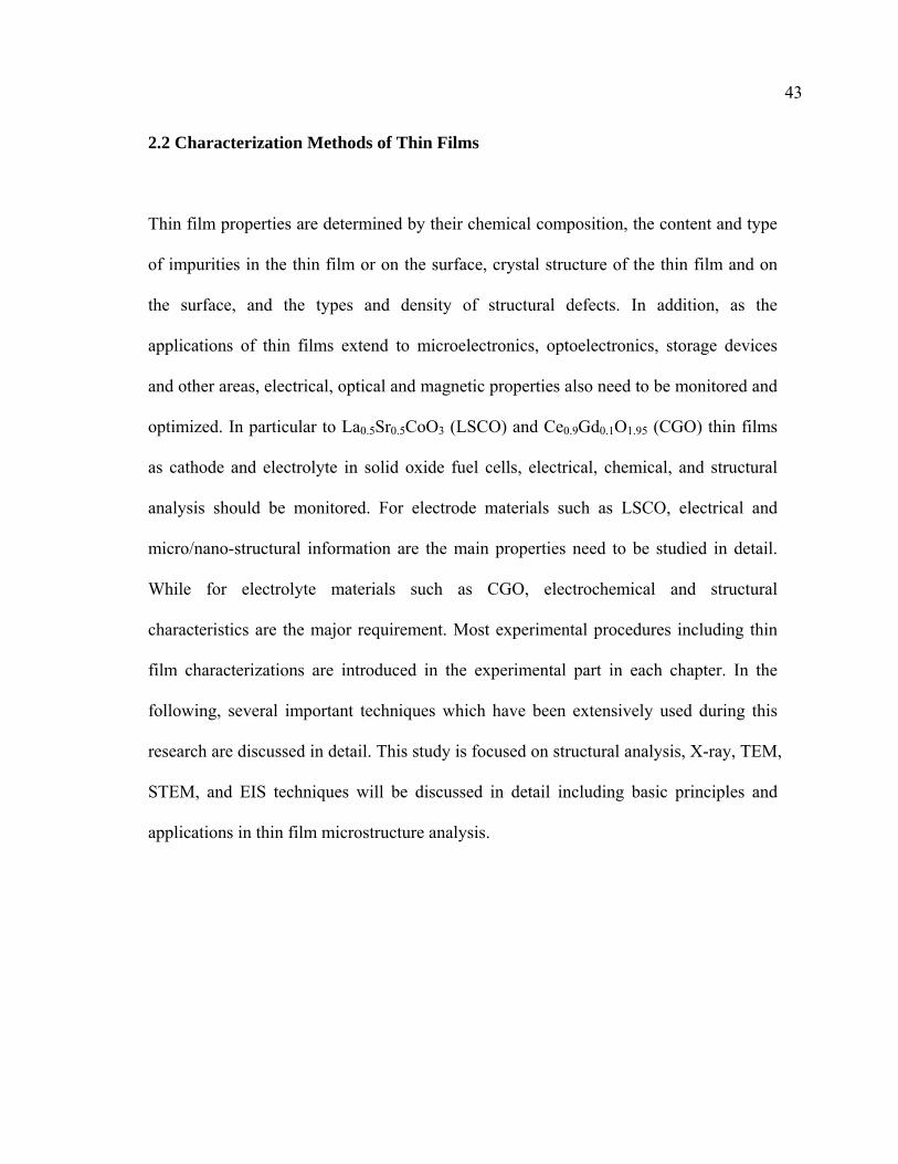
44
2.2.1 X-ray Diffraction (XRD: Structural Analysis)
X-ray diffraction is one of the most important nondestructive structural analysis
techniques used to probe and analyze the crystal structure of solids, including lattice
constant, orientation of single crystals, preferred orientations of thin films, identification
of unknown materials, defects, stress, etc. Basic mechanism of X-ray analysis is based
on that, when a parallel and monochromatic X-ray beam with a wavelength λ and angle
of incidence θ is diffracted by a set of planes which are oriented in specific directions
sharp peaks corresponding to the spacing between the planes appear when the Bragg’s
law conditions are satisfied:
n2 sind θ λ= (2.6)
These peaks are characteristic to materials and crystal structures. The crystal structure of
a specific material determines the diffraction pattern, and in particular the shape and size
of the unit cell determine the relative intensities of these lines. In the structural analysis
by using X-ray of known wavelength λ, and measuring θ, we can determine the “d”
spacing of various planes in the crystal. The essential features of an X-ray spectrometer
are shown in figure 2.5. It should be noted that the incident beam, normal to the
reflecting plane, and the diffracted beam are always coplanar; and the angle between the
diffracted beam and the transmitted beam is always 2θ.
45
Fig.2.5. Schematic of X-ray spectrometer [42]
Incident X-rays from the tube T on a crystal C which can be set to any desired angle
with respect to the incident beam by rotation about an axis O at the center of the
spectrometer circle are diffracted from the crystal and detected at the detector D. D is a
counter which measures the intensity of the diffracted x-rays, it can rotate around center
axis O and set at any desired angular position. Thus by measuring the peak positions,
one can determine the shape and lattice parameters of the unit cell, and by measuring the
intensities of the diffracted beams one can determine the positions of atoms within the
unit cell. Conversely, if the shape and the lattice parameters of the unit cell of the crystal
are known, we can predict the positions of all the possible peaks of the film [42].
In the application of the Bragg’s Law, certain ideal conditions are assumed, for example,
the crystal is perfect and the incident beam consists of strictly parallel and purely
monochromatic radiation. It should be noted that only an infinite crystal can be
considered as a perfect crystal. This comes from the fact that the waves involved in
46
diffraction reinforce each other and there is a contribution for the destructive
interference from the planes deeper into crystal. Destructive interference is therefore a
consequence of the periodicity of atom arrangement just as much as it is the constructive
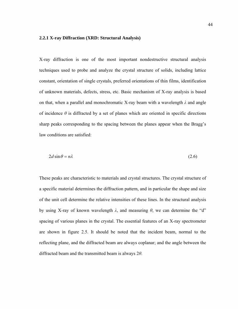
interference. As a result the width of the diffraction curve increases as the thickness of
the crystal decreases. Schematic representation of the effect of the fine particle size on
diffraction curves is shown in figure 2.6. The following expression gives the estimate of
the particle size of very small crystals from the measured width of their diffraction
curves: 0.9cos B
tB
λθ
= , where B = θ 1−θ 2, ( from figure 2.6) is the width i.e. the
difference between the two extreme angles at which the intensity is zero.
Fig.2.6. Effect of fine particle size on diffraction curve [42]
Another possible cause of line broadening of the x-ray line is the natural “spectral
width” of the x-ray source which is proportional to tanθ and becomes quite obvious as θ
47
approaches 90o. The existence of the mosaic structure of the crystal or film can also
influence the line broadening of the X-ray. Thus if the angle of misorientation between
the blocks of the mosaic structure is ε , the diffraction will occur not only at an angle of
incidence θB but also it will appear in all the angles between θB and θB+ ε . Another
effect of the mosaic structure is an increase in the intensity of the reflected beam with
respect to theoretically calculated value for an ideally perfect crystal.
The diffracted beam is stronger than the sum of all the rays scattered in the same
direction, because of the reinforcement (strengthening) of the diffracted beams, but
extremely weak compared to the incident beam. If the scattering atoms are not arranged
in a regular and periodic way then the diffracted x-rays will have a random phase
relationship to one another and neither constructive nor destructive interference will
happen under such conditions. Then the intensity of a beam scattered in a particular
direction is simply the sum of intensities of all X-rays scattered in that direction. If there
are N scattered rays and each ray has amplitude A and therefore with intensity A2 in
arbitrary units, then the intensity of the scattered beam is NA2. However, if the rays are
scattered by atoms of a crystal to a direction satisfying the Bragg’s Law, then they are all
in the same phase and the amplitude of the scattered beam will be N times the amplitude
A of each scattered X-ray or NA. Therefore the intensity of the scattered beam is N2A2,
or N times larger than the case where no reinforcement occurred. This explains why the
X-ray intensity of a crystal is much higher than that of an amorphous solid.

48
As mentioned earlier the intensities of the diffracted beams are determined by the
positions of the atoms in the unit cell. Since the X-rays are scattered by electrons and all
the atoms in the unit cell establishing an exact relationship between intensity and atomic
positions is a complex problem because of many variables involved in the scattering
process. When a monochromatic beam of X-rays strikes an atom, two scattering
processes occur. Tightly bound electrons go into oscillation and radiate X-rays of same
wavelength as that of the incident beam (coherent scattering). More loosely bound
electrons scatter part of the incident beam and slightly increase their wavelength to a
certain extent depending on the scattering angle (incoherent angle). Since the intensity of
the coherent scattering is inversely proportional to the square of the mass of the
scattering particle, the net effect of the coherent scattering by an atom occurs only from
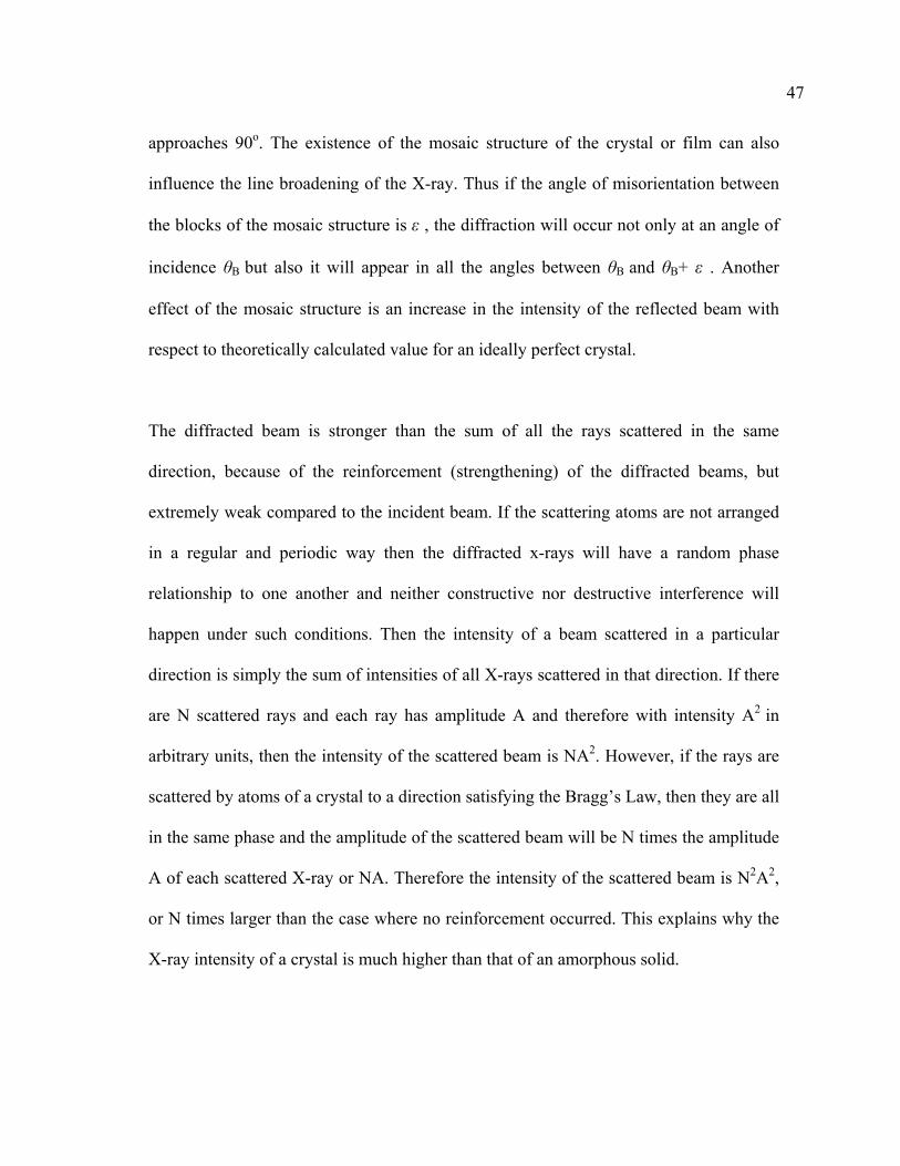
the scattering by the electrons contained in the atom. The atomic scattering factor f,
describes the efficiency of scattering of a given atom in a given direction, where f~sinθ/λ,
and the values for f for various atoms and various values of sinθ/λ are tabulated. A
typical variation for f in the case of Cu is shown in Fig. 2.7. The coherently scattered
radiation from all the atoms undergoes reinforcement (constructive interference) to
certain directions, and thus produces diffracted beams.
49
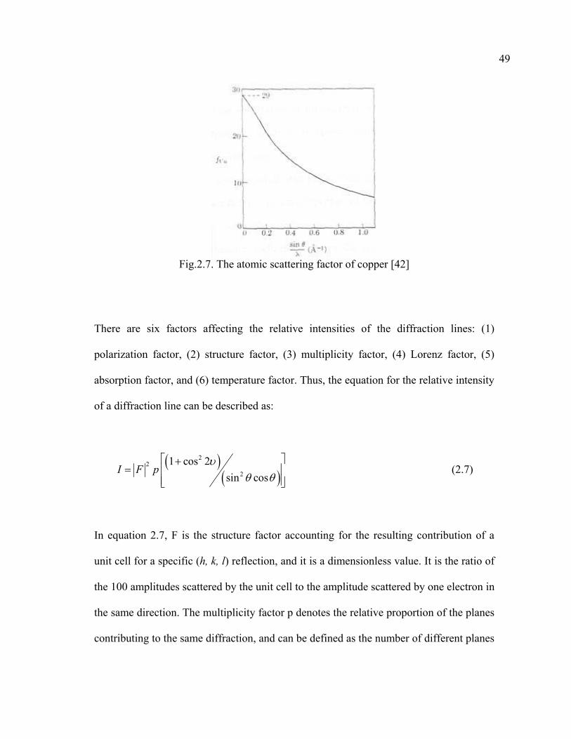
Fig.2.7. The atomic scattering factor of copper [42]
There are six factors affecting the relative intensities of the diffraction lines: (1)
polarization factor, (2) structure factor, (3) multiplicity factor, (4) Lorenz factor, (5)
absorption factor, and (6) temperature factor. Thus, the equation for the relative intensity
of a diffraction line can be described as:
( )( )
22
2
1 cos 2sin cos
I F pυ
θ θ
⎡ ⎤+= ⎢
⎢ ⎥⎣ ⎦ ⎥ (2.7)
In equation 2.7, F is the structure factor accounting for the resulting contribution of a
unit cell for a specific (h, k, l) reflection, and it is a dimensionless value. It is the ratio of
the 100 amplitudes scattered by the unit cell to the amplitude scattered by one electron in
the same direction. The multiplicity factor p denotes the relative proportion of the planes
contributing to the same diffraction, and can be defined as the number of different planes
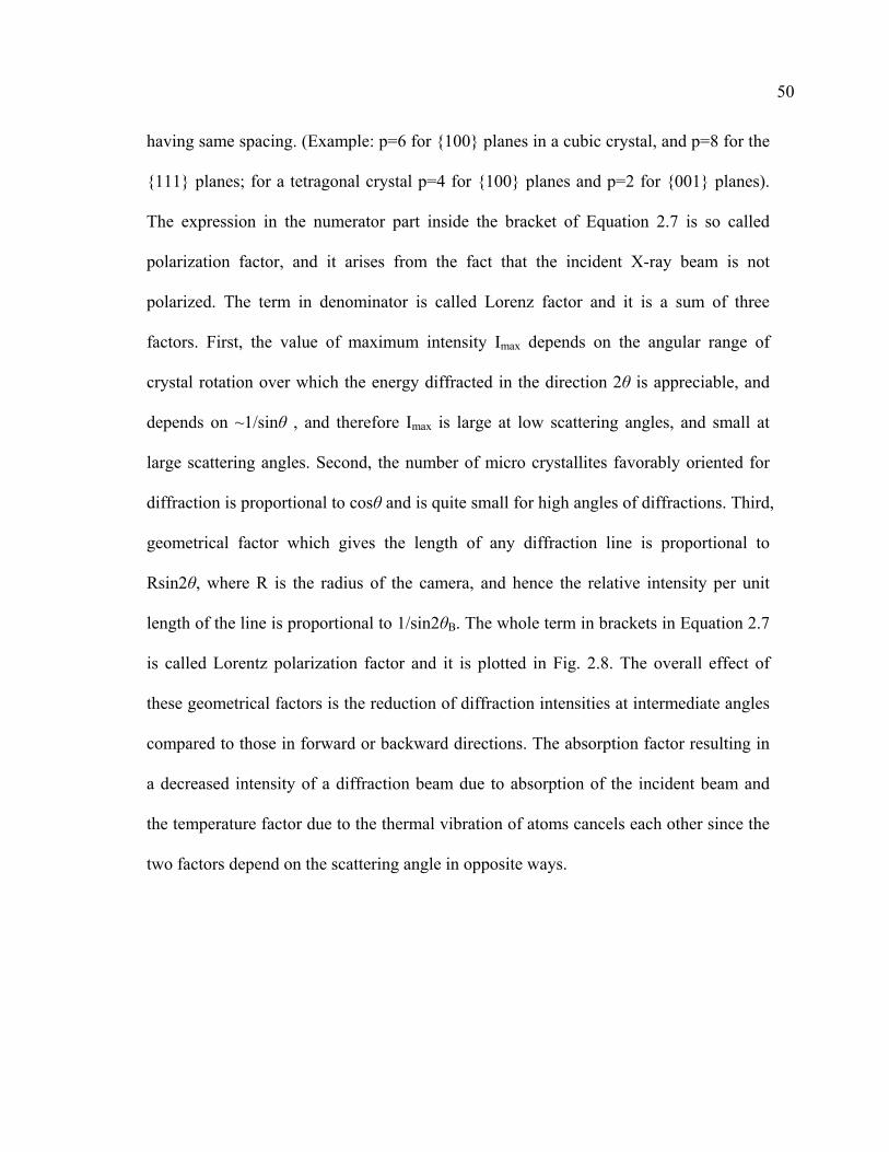
50
having same spacing. (Example: p=6 for 100 planes in a cubic crystal, and p=8 for the
111 planes; for a tetragonal crystal p=4 for 100 planes and p=2 for 001 planes).
The expression in the numerator part inside the bracket of Equation 2.7 is so called
polarization factor, and it arises from the fact that the incident X-ray beam is not
polarized. The term in denominator is called Lorenz factor and it is a sum of three
factors. First, the value of maximum intensity Imax depends on the angular range of
crystal rotation over which the energy diffracted in the direction 2θ is appreciable, and
depends on ~1/sinθ , and therefore Imax is large at low scattering angles, and small at
large scattering angles. Second, the number of micro crystallites favorably oriented for
diffraction is proportional to cosθ and is quite small for high angles of diffractions. Third,
geometrical factor which gives the length of any diffraction line is proportional to
Rsin2θ, where R is the radius of the camera, and hence the relative intensity per unit
length of the line is proportional to 1/sin2θB. The whole term in brackets in Equation 2.7
is called Lorentz polarization factor and it is plotted in Fig. 2.8. The overall effect of
these geometrical factors is the reduction of diffraction intensities at intermediate angles
compared to those in forward or backward directions. The absorption factor resulting in
a decreased intensity of a diffraction beam due to absorption of the incident beam and
the temperature factor due to the thermal vibration of atoms cancels each other since the
two factors depend on the scattering angle in opposite ways.
51
Fig.2.8. Lorentz-polarization factor vs. Bragg angle [42]
The properties (mechanical, electrical, chemical, etc.) of a single phase aggregate are
determined by two factors, the properties of the single crystal of the material and the
way in which the single crystals are put together to form composite mass. Thus the
relative size, perfection, and orientation of the grains make up the aggregate or the film
determine the properties of the materials.
The size of grains in a polycrystalline material has a distinct effect on many of its
properties, such as increase in strength and hardness with the reduction of the grain size.
X-ray diffraction can give semi-quantitative information about the grain size along with
the information about the crystal perfection and orientation. X-ray diffraction line
broadening can occur because of the size effect of the crystal grains. The diameter of the
crystal particle ‘t’ is then measured as 0.9cosB
λθ , where B is the line broadening. The
crystal perfection or the effect of both uniform and non-uniform strain also determines

52
the diffraction line position and shape as shown in Fig. 2.9. If the grain or film is under
uniform tensile strain at right angles to the reflecting planes, their spacing become larger
than d0, and the corresponding diffraction line shifts to lower angles, but the shape does
not change. However, under non-uniform strain (on the top tension, one the bottom
compression) line broadening occurs.
And finally, intensity distribution of lines parallel to the substrate surface can give the
information about the presence or absence of a preferred orientation in the film. In such
a case the only grains which can contribute to the hkl reflection are ones with (hkl)
planes parallel to the substrate surface. If a texture has only a few such grains then the
intensity of the hkl reflection will be very low. Film planes which are preferentially
oriented as parallel or nearly parallel to the film surface would show extremely high
intensity of the hkl planes.
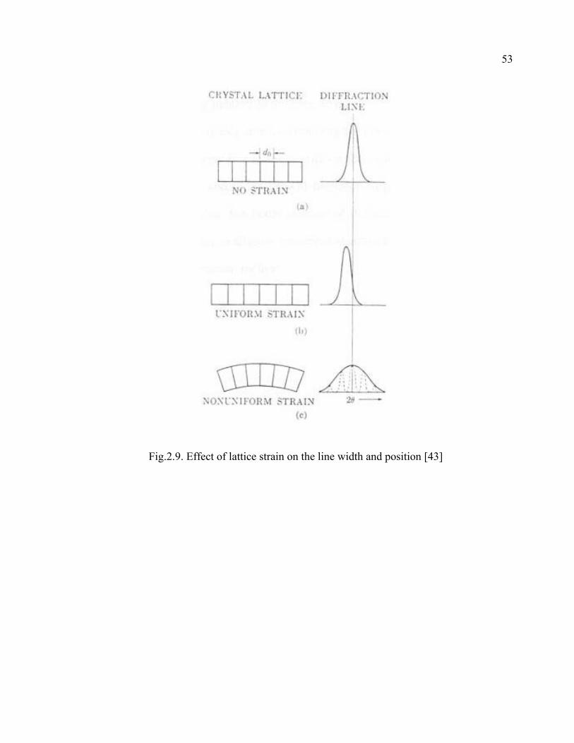
53
Fig.2.9. Effect of lattice strain on the line width and position [43]

54
2.2.2 Transmission Electron Microscopy (Structural: TEM)
Transmission electron microscopy (TEM) is a method used in obtaining structural and
morphological information of specimens which are thin enough for electrons to transmit
through. This technique can help our understanding of materials by providing us with the
detailed micro structure down to the atomic levels. Application of TEM is not only
limited in materials science research. It can also be used in the semiconductor device
technology, biotechnology, and other material or microstructure related field. For
example, TEM has been extensively used in device fabrication to provide information
about the geometry of patterned films, the uniformity of thickness and coverage, in
addition to surface morphology and topography, including size and shape, and presence
of compounds. Especially ever since the nano-technology has been introduced to the
device fabrication, the resolution of SEM and other normal surface probing techniques
can not satisfy the requirements of detailed atomic structure study. TEM has become the
most important technique which can probe detail structural and defect information.
Additionally, TEM can also give cross-sectional view of interface regions which can
give information about the interfacial reactions, perfection of devices, and diffusion
study. When it is combined with other analytical techniques, such as STEM, EELS, and
EDX TEM is a very powerful material characterization technique which can combine
imaging and chemical compositional study down to a single atom(or a column of atoms,
strictly speaking). For example, JEOL 2010FEG has point to point resolution of 0.18 nm.
In this section, major parameters of TEM are listed. Several important imaging and
55
diffraction techniques are discussed and related examples for different techniques are
presented.
Resolution and Aberration
The main parameter of a transmission electron microscope is its resolution and
magnification. Magnification can be increased easily by increasing acceleration voltage
of TEM but increasing resolution is rather a hard work due to many related parameters.
When there is no aberration of lenses classical Raleigh criterion describes the smallest
distance that can be resolved approximately by:
0.61sin
λδ μ β= (2.8)
where λ is the wavelength of the radiation, μ the refractive index of the viewing medium,
and β is the semi-angle of collection of the magnifying lens. Due to the coherency of
electron beam in TEM and the short wavelength of the accelerated electrons (λ is in the
order of hundredths of an Å), the resolution limit is down to 1 Å (for 1MeV electrons
λ=0.0087 Å, and a=5x10⁻³ radian).
Along with the chromatic aberration and the stigmatism, spherical aberration is one of
the main electromagnetic lens defects that limit the resolution of the electron microscope
as shown in figure 2.10 a. The spherical aberration is a lens defect arising from the non-
paraxiality of the electron beam which cause electrons to leave the point P at higher
56
angles with respect to the optic axis of the microscope and to focus before the image
plane, while electrons left the objective lens closer to the optic axis are focused on the
image plane. Thus instead of a point focus a disk with a radius rs is formed, where rs=Cs
β2, β is the angular aperture of the lens.
Chromatic aberration arises from the non-chromaticity of the electron beam. Non
chromaticity is the energy difference among electrons. Electrons leaving the electron
gun have slightly different energies and the difference ΔE is a bout 3eV. This causes the
faster electrons to be less refracted from the objective lens than the lower energy
electrons, as shown in figure 2.10 b. The higher energy electrons thus are brought in
focus beyond the image plane.
Astigmatism arises from the asymmetric magnetic field and it occurs when the lens
exhibits different focal lengths, depending on the plane of the ray paths. Thus in the
figure 2.10 c the rays traveling plane A are focused at PA while the rays in plane B
focused at point PB. Because of this astigmatixm a point on the object is imaged as a
disk with radius rA=βΔfA, where ΔfA is the maximum difference in focal length arising
from astigmatism. If all the astigmatisms can be corrected, the sample is thin enough,
and chromatic aberration is negligible then the resolution is limited by the spherical
aberration error. The resolution is governed by the combination of Rayleigh criterion and
the aberration error.

57
Fig.2.10. Objective aberration (a) Spherical, (b) chromatic, (c) astigmatism [44]
(2.9)
This equation describe the practical resolution of the microscope. Where ‘r’ is the
spherical aberration error, and Cs is the spherical aberration, λ is the wavelength of
electron.
( )0.253min 0.91 sr C λ=
58
Depth of Field and Depth of Focus
Depth of field D is the value on both sides of the theoretical object plane P of the
objective lens within which the resolution can be maintained. A specimen shift of D/2
with respect to the object plane P results in a disc of radius 2
aDr =
solution di
eans the better focusing over a larger
where ‘a’ is the
objective angular aperture. In order to keep the resolution from diminishing, the
diameter of this disk should be smaller than or equal to the re stance‘d’, so that
aD = d. The larger depth of focus (D~500Å) m
range of the specimen thickness. Depth of focus ‘D' is defined similarly in the final
image plane as depth of field in the object plane. Now d'=dM and ' aaM
= , where M is
the final magnification. Thus depth of focus D'=DM2. Magnification of the order of 105
would give about 500m depth of focus.
Image and Diffraction Modes
The objective lens takes the electrons exiting from the exit surface of the specimen,
disperses them to create a diffraction pattern (DP) in the back focal plane, and
recombines them to form an image in the image plane. To see the diffraction pattern you
have to adjust the imaging system lenses so that the back focal plane for the intermediate
lens can be the image plane. Then the diffraction pattern is projected onto the viewing
screen, see figure 2.11 A. For imaging mode, you readjust the intermediate lens so that
its object plane is the image plane of the objective lens. Then the image is projected onto
the viewing screen, as shown in 2.11 B.
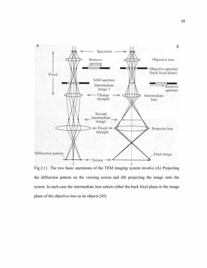
59
Fig.2.11. The two basic operations of the TEM imaging system involve (A) Projecting
the diffraction pattern on the viewing screen and (B) projecting the image onto the
screen. In each case the intermediate lens selects either the back focal plane or the image
plane of the objective lens as its objects [45]

60
Image Mode and Image Contrast
The image contrast in TEM arises because of the scattering of the incident beam by the
specimen. As the electron beam transverse the specimen it changes both its amplitude
and phase and the image contrast occurs because of these changes. There is a
fundamental distinction between amplitude contrast and phase contrast which can both
contribute to the image. The amplitude contrast can be divided into mass-thickness
contrast and diffraction contrast according to Williams and Carter’s descriptions.
Diffraction contrast is most widely used in identifying defects and distinguishing
different types of crystal defects. Diffraction contrast occurs because of coherent elastic
scattering at special (Bragg) angles. The intensity in a diffracted beam depends strongly
upon the deviation parameter ‘s’. Since the crystal defects distort the diffracting planes
the diffraction contrast from regions close to the defect depends on the properties of the
defects such as strain field. The specimen has to be tilted into two-beam conditions in
order to get good interpretable diffraction contrast. Mass-thickness contrast arises from
incoherent Rutherford elastic scattering of electrons. Any scattered beam can contribute
to the formation of the image.
Two-Beam Conditions, Bright Field and Dark Field
Bright field and dark field are specific imaging conditions when the specimen is tilted so
that only one diffracted beam is strong. When the electrons in the strongly excited beam
have been diffracted by a specific set of hkl planes the area that appears bright in the
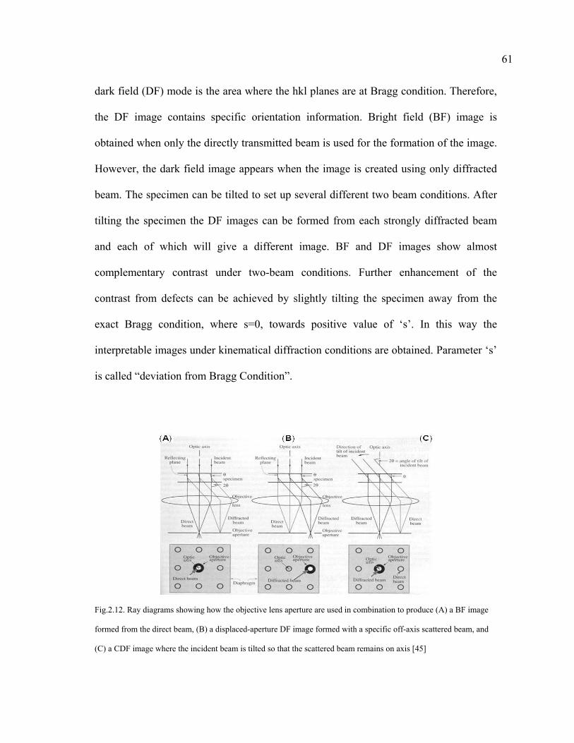
61
dark field (DF) mode is the area where the hkl planes are at Bragg condition. Therefore,
the DF image contains specific orientation information. Bright field (BF) image is
obtained when only the directly transmitted beam is used for the formation of the image.
However, the dark field image appears when the image is created using only diffracted
beam. The specimen can be tilted to set up several different two beam conditions. After
tilting the specimen the DF images can be formed from each strongly diffracted beam
and each of which will give a different image. BF and DF images show almost
complementary contrast under two-beam conditions. Further enhancement of the
contrast from defects can be achieved by slightly tilting the specimen away from the
exact Bragg condition, where s=0, towards positive value of ‘s’. In this way the
interpretable images under kinematical diffraction conditions are obtained. Parameter ‘s’
is called “deviation from Bragg Condition”.
Fig.2.12. Ray diagrams showing how the objective lens aperture are used in combination to produce (A) a BF image
formed from the direct beam, (B) a displaced-aperture DF image formed with a specific off-axis scattered beam, and
(C) a CDF image where the incident beam is tilted so that the scattered beam remains on axis [45]
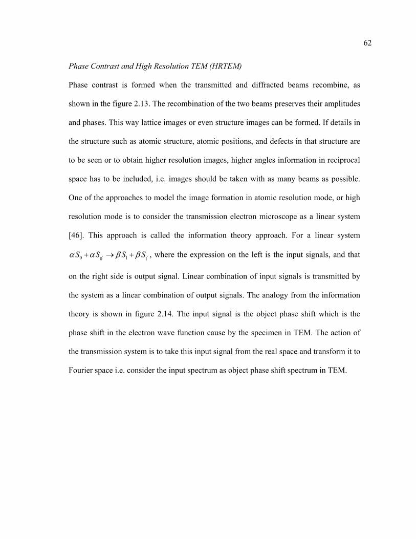
62
Phase Contrast and High Resolution TEM (HRTEM)
Phase contrast is formed when the transmitted and diffracted beams recombine, as
shown in the figure 2.13. The recombination of the two beams preserves their amplitudes
and phases. This way lattice images or even structure images can be formed. If details in
the structure such as atomic structure, atomic positions, and defects in that structure are
to be seen or to obtain higher resolution images, higher angles information in reciprocal
space has to be included, i.e. images should be taken with as many beams as possible.
One of the approaches to model the image formation in atomic resolution mode, or high
resolution mode is to consider the transmission electron microscope as a linear system
[46]. This approach is called the information theory approach. For a linear system
'1'0 10S S S Sα α β β+ → + , where the expression on the left is the input signals, and that
on the right side is output signal. Linear combination of input signals is transmitted by
the system as a linear combination of output signals. The analogy from the information
theory is shown in figure 2.14. The input signal is the object phase shift which is the
phase shift in the electron wave function cause by the specimen in TEM. The action of
the transmission system is to take this input signal from the real space and transform it to
Fourier space i.e. consider the input spectrum as object phase shift spectrum in TEM.
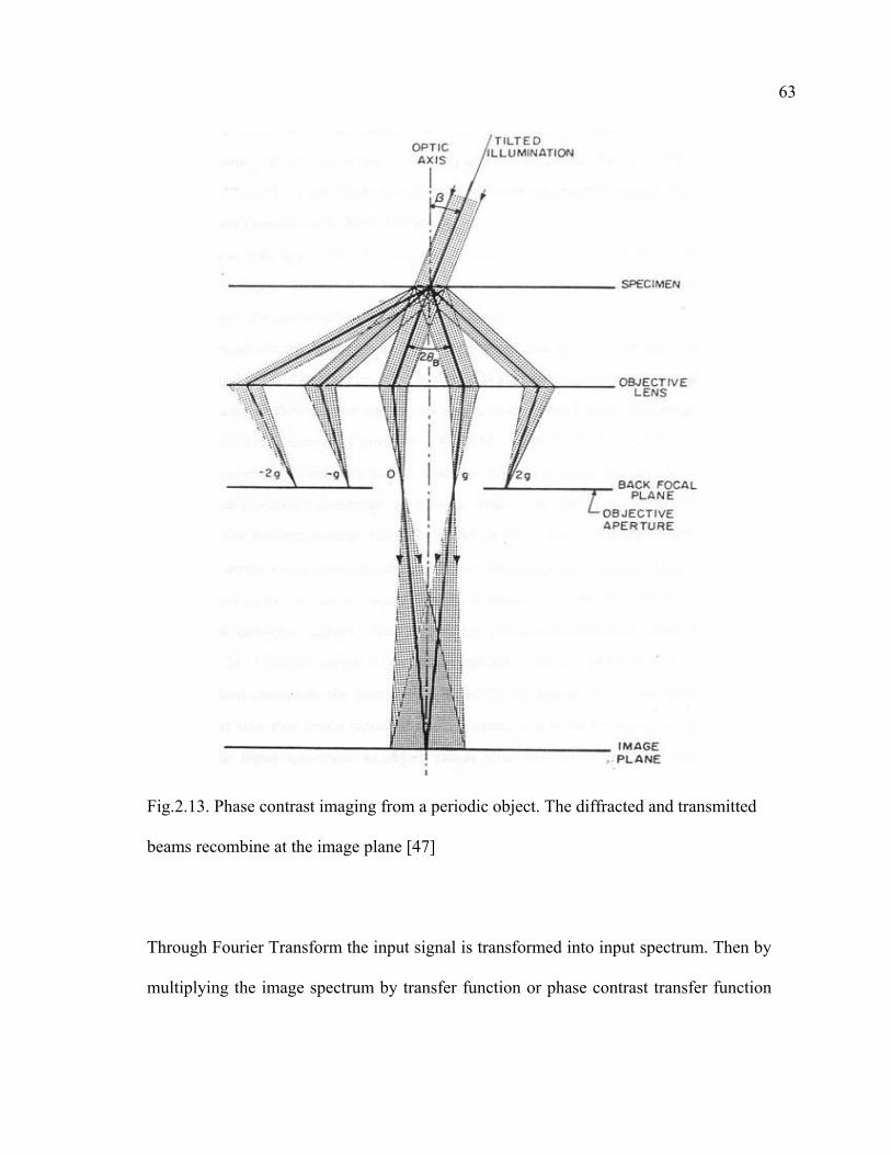
63
Fig.2.13. Phase contrast imaging from a periodic object. The diffracted and transmitted
beams recombine at the image plane [47]
Through Fourier Transform the input signal is transformed into input spectrum. Then by
multiplying the image spectrum by transfer function or phase contrast transfer function
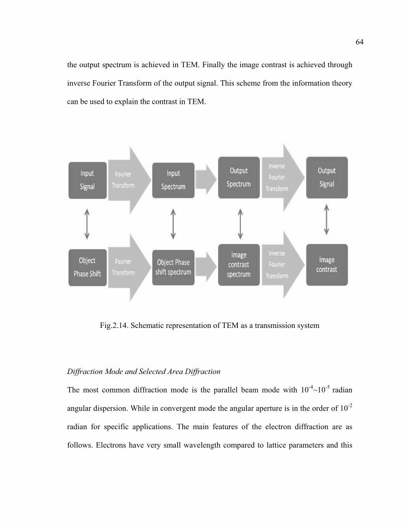
64
the output spectrum is achieved in TEM. Finally the image contrast is achieved through
inverse Fourier Transform of the output signal. This scheme from the information theory
can be used to explain the contrast in TEM.
Fig.2.14. Schematic representation of TEM as a transmission system
Diffraction Mode and Selected Area Diffraction
The most common diffraction mode is the parallel beam mode with 10-4~10-5 radian
angular dispersion. While in convergent mode the angular aperture is in the order of 10-2
radian for specific applications. The main features of the electron diffraction are as
follows. Electrons have very small wavelength compared to lattice parameters and this
65
s: 2 / / hkln dθ λ=
atter so the
results in small diffraction angles. Thus the Bragg equation become , at
the diffraction angle 2θ 1o. Electrons interact very strongly with the m
kinematic approximation does not apply. Very thin specimen is used in transmission
electron diffraction and the resulting diffraction domains are in the form of fine rods
perpendicular to the specimen. To achieve a hkl reflection, the reflection sphere has to
intersect the corresponding diffraction domain. The observed reflections have the
incident direction [uvw] as a zone axis relative to the lattice planes (hkl) and therefore
the reflection indices obey the following expression for the zero Laue zone:
(2.10)
This is an equation of the reciprocal lattice plane (uvw) passing through the origin and
containing lattice point hkl.
≅
0hu kv lw+ + =
66
Selected Area Electron Diffraction (SAD)
Depending on the adjustment of the post objective lenses such as intermediate lens and
diffracted lens on one of the planes, either the electron diffraction pattern or the electron
image of the object is displayed on the final viewing screen or the film. The selected
aperture inserted into the image plane limits the diameter ( )' ssd d m=
eter (ds=1μ
age selection area '
of an image
selection area. Choosing a given aperture results in selecting a specific area of the
specimen. The active area of SAD is in the order of microm m), so with
magnification of the objective lens 100 (m=100), the ims
d is 100 μm.
The diffraction length L is not directly expressed. If we know that ΔL=dR the diffraction
constant or camera constant K (=ΔL), which describes the magnification of the
diffraction pattern, can be determined from standard specimen. Where R is the distance
between the transmitted beam and the diffracted spot corresponding to interplanar
distance d. The diffraction mode can be utilized in many other sub modes such as
selected-area electron diffraction, micro diffraction or nano diffraction, and convergent
beam electron diffraction etc.
67
2.2.3 Scanning Transmission Electron Microscopy (STEM): Structural and
Elemental Analysis Using Z-Contrast
In scanning transmission electron microscopy (STEM), Z-contrast techniques can
provide strong compositional sensitivity results at atomic level. To achieve bright field
STEM image transmitted beam is used. To obtain Z-contrast dark field images high-
angle Rutherford-scattered electrons are collected by high angle annular dark field
detector. In obtaining atomic resolution Z-contrast image probe size is critical. STEM
imitates the parallel beam in a TEM by scanning strictly parallel to the optical axis at all
times. The key feature of STEM is that the scanning beam does not change direction
when the beam is scanned. Fig. 2.15 illustrates how the STEM achieves the parallel
beam. Two pairs of scan coils are used to pivot the beam about the front focal plane of
the upper objective (C3) pole piece. Then the C3 lens ensures all electrons emerging
from the pivot point to be brought parallel to the optic axis and the C1 lens crossover
image is formed in the specimen plane. If the objective lens is symmetrical then a
stationary diffraction pattern is formed on the back focal plane. One big advantage of
forming images this way is that there is no need for lenses in an SEM so defects in the
imaging lenses do not affect image resolution. Image resolution is controlled by beam
only [48-52].
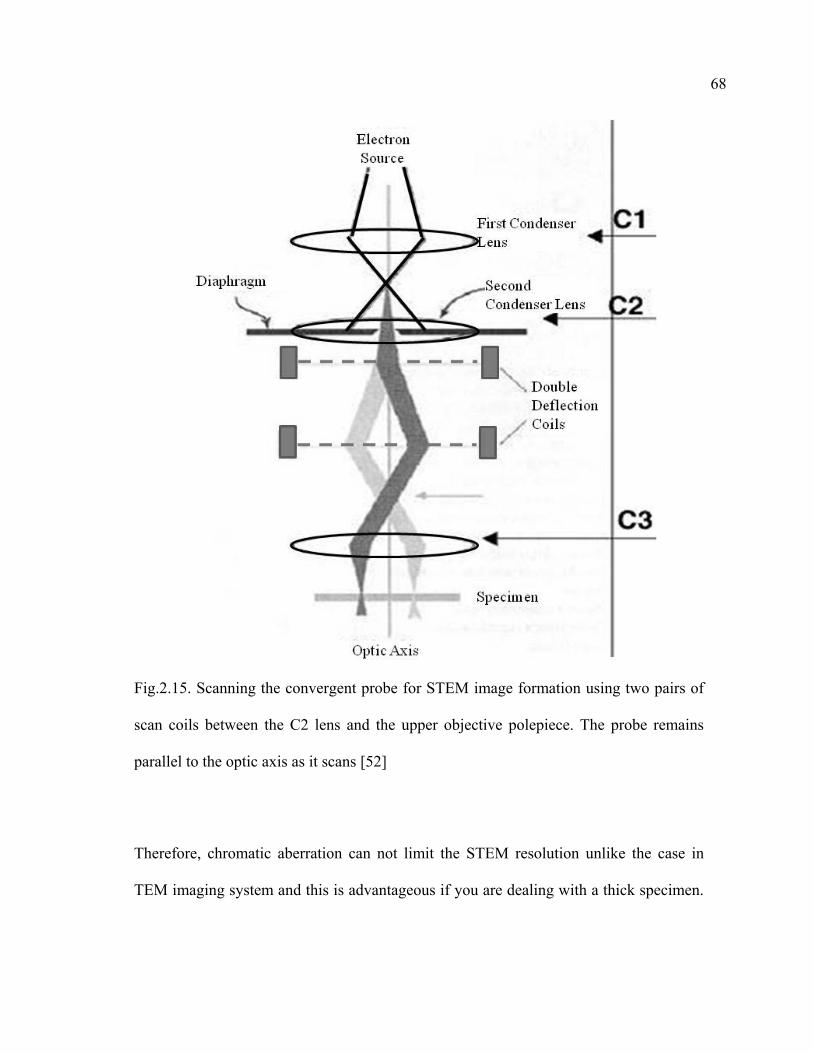
68
Fig.2.15. Scanning the convergent probe for STEM image formation using two pairs of
scan coils between the C2 lens and the upper objective polepiece. The probe remains
parallel to the optic axis as it scans [52]
Therefore, chromatic aberration can not limit the STEM resolution unlike the case in
TEM imaging system and this is advantageous if you are dealing with a thick specimen.
69
Similar to TEM techniques, STEM can form its own bright field (BF) and dark field
(DF) images.
Bright Field STEM Images
The basic principle of image formation in the scanning mode is fundamentally different
from that of a static beam TEM imaging system. In the TEM, a portion of the electrons
transmitted through an area of the specimen is selected and the distribution is projected
onto a screen. While in STEM, by adjusting the scan coils the specimen is scanned by
the beam. These same coils are used to scan the CRT synchronously. The electron
detector is used as a interface between the electrons coming from the specimen and the
image viewed on the CRT. Since it scans up to 2048 scan lines to construct an image on
the CRT, the whole process of the STEM imaging is much slower than TEM imaging. In
order to form a BF image in TEM an aperture is inserted into the plane of the TEM
diffraction pattern and only the electrons direct through it are allowed into the imaging
system [53-55]. In STEM mode an electron detector is used in exactly the same way as
the aperture in TEM. The detector only allows the desired electrons to hit the detector to
constitute the image.
70
Annular Dark Field Images
Annular dark-field (ADF) imaging is a method of mapping samples in a scanning
transmission electron microscope (STEM). Images are formed by collecting scattered
electrons with an annular dark-field detector in scanning transmission electron
microscopes [52].
For dark field imaging, the annular dark field detector collects a much larger number of
electrons than conventional dark field imaging in the TEM. This gives advantages of
signal collection efficiency and as a result lower electron dose required. As opposed to
Bragg scattered electrons, an annular dark field images, Z-contrast images, formed only
from very high angle and incoherently scattered electrons are highly sensitive to
variations in the atomic number of atoms in the sample. This technique is also known as
high angle ADF (HAADF). Annular detector, which surrounds the BF detector, is used
to collect the scattered electrons [56,57]. ADF detector is centered on the optics axis and
has a hole in the middle, within which the BF detector sits as shown in Fig. 2.16a. Fig.
2.16b shows the complementary ADF (c) and BF (d) images.
Magnification in STEM
Scanning images are not magnified by lenses. STEM magnification is controlled by the
scan dimensions on the specimen. This is an essential difference between scanning
imaging and static imaging. If the scanned area on the specimen is 1cm × 1cm, and the
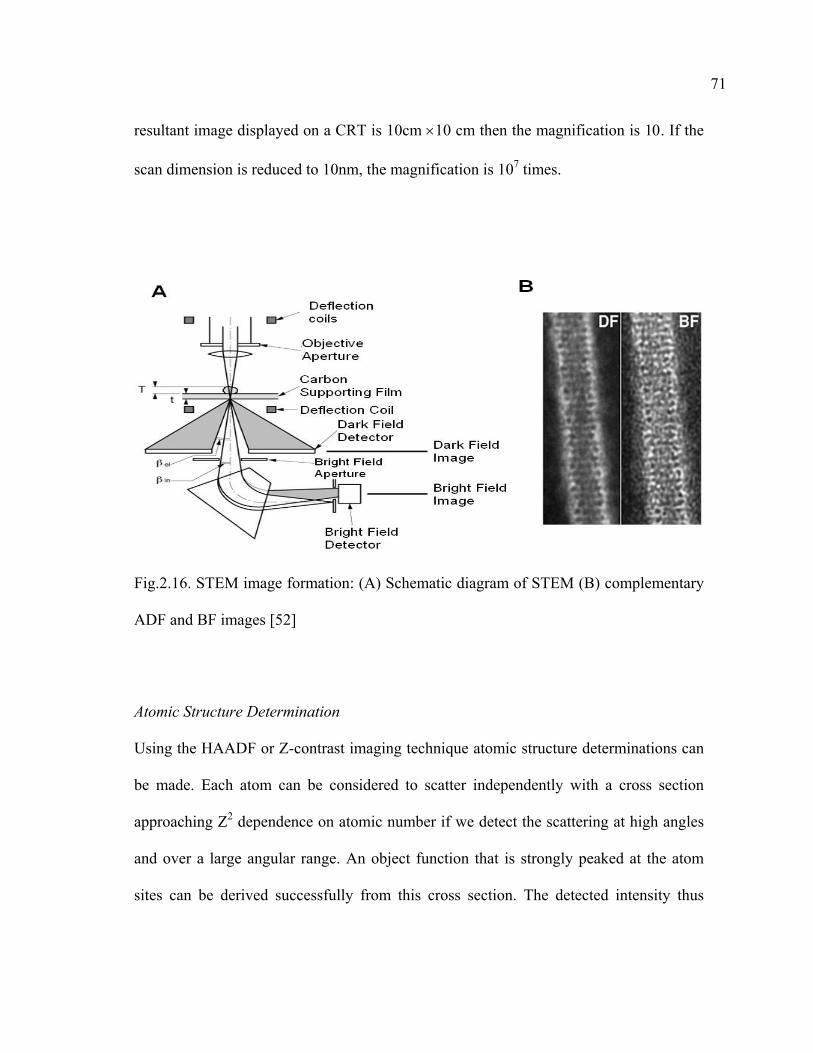
71
resultant image displayed on a CRT is 10cm ×10 cm then the magnification is 10. If the
scan dimension is reduced to 10nm, the magnification is 107 times.
Fig.2.16. STEM image formation: (A) Schematic diagram of STEM (B) complementary
ADF and BF images [52]
Atomic Structure Determination
Using the HAADF or Z-contrast imaging technique atomic structure determinations can
be made. Each atom can be considered to scatter independently with a cross section
approaching Z2 dependence on atomic number if we detect the scattering at high angles
and over a large angular range. An object function that is strongly peaked at the atom
sites can be derived successfully from this cross section. The detected intensity thus

72
consists of a convolution of this object function and the probe intensity profile. The
spatial resolution is limited only by the probe size of the microscope due to the small
width of this object function (~ 0.1Å) [58]. For a crystalline material in a zone-axis
orientation the atomic columns can be illuminated individually because of the greater
size of atomic spacing than the probe size. As the probe scans over the specimen an
atomic resolution compositional map is generated where the intensity depends on the
root mean square of atomic number of the atoms in the columns. If dynamic diffraction
only results in columnar channeling and simply scales the scattering cross sections of the
object function according to thickness then even for thicker specimens the same result
holds. The advantage of this methodology is that the changes in focus and thickness do
not cause contrast problems in the atomic resolution image [59]. So the atomic column
sites can be identified unambiguously during the experiment. With this method atomic
columns at grain boundaries can be located without the need for simulated images.
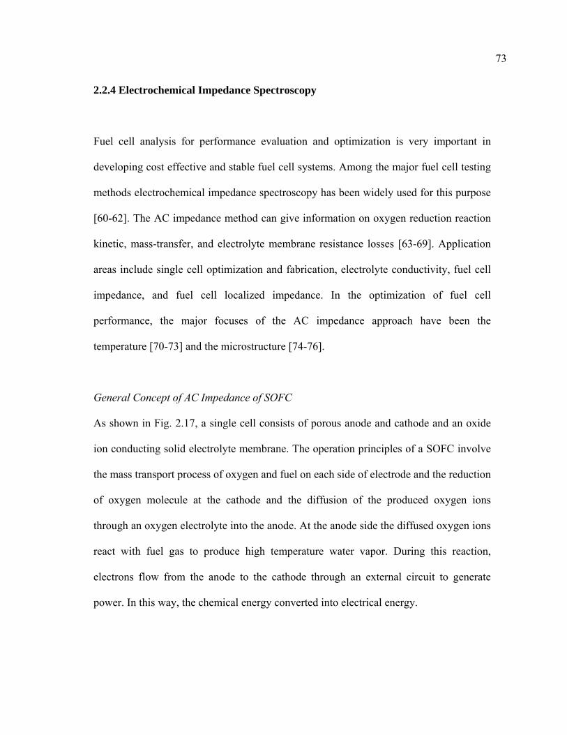
73
2.2.4 Electrochemical Impedance Spectroscopy
Fuel cell analysis for performance evaluation and optimization is very important in
developing cost effective and stable fuel cell systems. Among the major fuel cell testing
methods electrochemical impedance spectroscopy has been widely used for this purpose
[60-62]. The AC impedance method can give information on oxygen reduction reaction
kinetic, mass-transfer, and electrolyte membrane resistance losses [63-69]. Application
areas include single cell optimization and fabrication, electrolyte conductivity, fuel cell
impedance, and fuel cell localized impedance. In the optimization of fuel cell
performance, the major focuses of the AC impedance approach have been the
temperature [70-73] and the microstructure [74-76].
General Concept of AC Impedance of SOFC
As shown in Fig. 2.17, a single cell consists of porous anode and cathode and an oxide
ion conducting solid electrolyte membrane. The operation principles of a SOFC involve
the mass transport process of oxygen and fuel on each side of electrode and the reduction
of oxygen molecule at the cathode and the diffusion of the produced oxygen ions
through an oxygen electrolyte into the anode. At the anode side the diffused oxygen ions
react with fuel gas to produce high temperature water vapor. During this reaction,
electrons flow from the anode to the cathode through an external circuit to generate
power. In this way, the chemical energy converted into electrical energy.
74
Fig.2.17. SOFC single cell configuration
In the diagnosis of fuel cells impedance spectroscopy has become an essential
methodology. AC impedance is a more general concept of resistance. Its modulus and
phase depend on the excitation frequency. In the following, a simple one-to-one
mapping method is adopted to express the impedance of Z(jω). If we use a sinusoidal
voltage perturbation ( ) ( )0 sin 2e t E ftπ φ=
tem then accord
i(t) = I0 sin(
+ , during measurements to excite a linear
time-invariant (LTI) circuit sys ing to linear system theory [68, 77], we
can get an AC current response, 2πft +ψ), which has the same frequency as
and ( )e t . 0E φ denote the amplitude and the initial phase of ( )e t respectively. In the
75
same way, I0 and ψ denote the amplitude and the initial phase of i(t) respectively.
Normally, the expressions of voltage and current can be mapped and converted from a
time domain to a complex domain, ( ) ( )*0 exp 2e t E ftπ φ= + and ( ) (*
0 exp 2i t I ft )π ϕ= +
lex number e*(t) and i*(t)
e domain and the
ation is possible. If we
functions can be
,
respectively, where e(t) and i(t
respectively. Therefore, a simp
complex domain where we can access the fre
denote 2πf as ω and defi en the transform
expressed as follows:
) are the real part of comp
le one-to-one mapping between the tim
quency inform
ne as an angle frequency th
( ) ( )( ) ( )( )
*0
*0
expi t IA j je t E
ω ψ ϕ= = − (2.11)
( ) ( ) ( ) ( ) ( ) ( ) ( )cos sinj Y jexpY j Y j j Y jω φ φ= = ω φ ω+ (2.12) ω
( ) 0
0
IY jE
ω = and φ ψ ϕ= −
where |Y(jω)| represents the modulus of Y(jω) and corresponds to th
function between the excitation and response signals acco
Φ represents the phase of Y(jω) and corresponds to the phase transfer f
the excitation and response signals according to a frequency of
is used as an excitation signal and, similarly,
(2.13)
e amplitude transfer
rding to a frequency of f, and
unction between
f. If i(t) = I0 sin(2πft +ψ)
( ) ( )t0 sin 2e t E fπ φ+ is used as an output =
signal, we can define the following:
76
( ) ( )( )( )( )
( )( )*
0*
0
je t EZ j eIi tϕ φω −= = (2.14)
( ) ( ) ( ) ( ) ( ) ( ) ( )exp cos sinZ j Z j j Z j j Z jω ω φ ω φ ω φ= = + (2.15)
Both the modulus |Z(jω)| and the phase angle φ of Z(jω) are functions of frequency. In
general, Z(jω) is the AC impedance and Y(jω) is the admittance which are the inverse of
each other as in Y(jω) = 1/Z(jω). In fact, SOFC devices are complicated systems
containing chemical, electrochemical, and multiple mass-transfer processes. The
coupling of these complex processes makes the systems nonlinear. The relationship
between the voltage and the current at different frequencies in such a nonlinear system
does not directly follow the expressions obtained from a LTI system. For example, under
large excitation of the amplitude of voltage or current SOFC systems tend to show
strong nonlinear behavior in their interfacial responses. But if the applied AC voltage
amplitude Δe is less than a given thermal voltage [64] then the system can be considered
as a linear system since the basic differential equations that govern the response of the
fuel cell system become nearly linear. The approximate linearization can also be derived
based on the nonlinear circuit system analysis [68].
If the equivalent linear equations are known at every point of the steady-state
characteristic then the behavior of a non-linear system can be defined entirely in linear
terms [78, 79]. Hence, the local analysis of a non-linear system can be confined to the
field of linear system theory. From an experimental point of view, it is satisfactory to
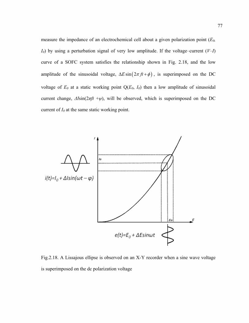
77
measure the impedance of an electrochemical cell about a given polarization point (E0,
I0) by using a perturbation signal of very low amplitude. If the voltage–current (V–I)
curve of a SOFC system satisfies the relationship shown in Fig. 2.18, and the low
amplitude of the sinusoidal voltage, ( )sin 2E ftπ φΔ + , is superimposed on the DC
voltage of E0 at a static working point Q(E0, I0) then a low amplitude of sinusoidal
current change, ΔIsin(2πft +ψ), will be observed, which is superimposed on the DC
current of I0 at the same static working point.
Fig.2.18. A Lissajous ellipse is observed on an X-Y recorder when a sine wave voltage
is superimposed on the dc polarization voltage
78
When we focus on the vicinity of a static work point (E0, I0) of the nonlinear system, the
Taylor expansion of the voltage, e, can be expressed as
( ) ( )0 0 0 0
22
2, ,
12E I E I
de d ee i idi d i
⎛ ⎞⎛ ⎞Δ = Δ + Δ +⎜ ⎟⎜ ⎟⎝ ⎠ ⎝ ⎠
(2.16)
If the amplitude of the perturbation signal is small enough, the higher order terms in Eq.
2.16) will be negligible compared to the first term. Therefore, Eq. (2.16) can be reduced
approximately to the first term of the expression, ( )( )0 0,E I
dee idiΔ = = Δ , and de/di is
roughly regarded as a constant around the static work point of Q(E0, I0). This process is
known as quasi-linearization. Therefore, under the condition that the amplitude of the
perturbation signal is smaller than the required value a SOFC may be treated as a linear
system with respect to the AC impedance measurement [64]. If the two sine waves are
plotted on an X-Y recorder, a Lissajous figure (ellipse) similar to that shown in Fig 2.18
can be observed. Hence by measuring the electrochemical impedance all along the
polarization curve we can perform a complete characterization of the interface and this
will enable us to compare the data with a model.
When an excitation current or voltage signal is supplied to a SOFC, a corresponding
output signal, which is determined by the coupling of electrical, chemical,
electrochemical, and mass transport processes, gives a characteristic impedance, Z(jω) =
Z’ + jZ”. Z(jω) is also called the transfer function of the SOFC system, and it represents
79
the amplitude and the phase shift relationship between the excitation and response
signals in terms of the frequency of ω (=2πft) [63].
Theoretically, this transfer function Z(jω) will have physical meaning only under the
following preconditions [80-82]. First, the response of the system must be related to the
excitation signal only. Second, Z(jω) is meaningful only when the excitation/response of
the system is described by a set of ‘linear’ differential laws. This means the impedance
of the system must be independent of the excitation signal magnitude. Third, the system
must be able to return to its original state when the perturbation is removed and the
system is stable. Forth, the impedance must be finite for all values of ω, including ω→0
and ω→∞. Because of high complexity of a SOFC system fitting all these preconditions
perfectly may not be possible. Therefore, when EIS is used for SOFC diagnosis some
special issues must be considered in advance.
The physicochemical processes within a SOFC can be divided into two categories as
internal factors and external factors. Materials and their composition, microstructures,
and component sizes are internal factors on the other hand factors such as temperature,
pressure, mass transport and concentrations can be categorized into external factors. The
measured impedance ‘Z(jω)’ is the overlapped responses of both the internal and
external factors and this implies that there is an inherent relationship between Z(jω) and
SOFC characteristics. For example, the measured impedances can give information
about fuel cell reaction kinetics such as reaction activation, electrolyte resistance, mass-

80
transfer efficiency, and operation conditions. With all these data SOFC performance and
failure modes can be diagnosed. Based on the diagnosis, fuel cell performance can be
improved by proper choice of material, microstructure engineering of the component
materials and component structure optimization. In addition, the failure mode
identification can be used to improve our fundamental understanding of the SOFC
operating mechanism and can be used for further improvement of the system. Since the
SOFC system has its own limitation in meeting the requirements of the transfer function
‘Z(jω)’, one has to be sure that the approximations are rational when processing the AC
impedance data.
Measurement of SOFC AC Impedance
Generally, four types of impedance data are measured. The four types are the
time/frequency domain measurement [64,77], in/ex situ measurement [64, 68], static and
instantaneous impedance measurement [83-87], and linear/non linear measurement [88,
89]. Rapid advances in digital signal processing techniques in recent years have made
possible the time domain method. However, measuring in the frequency domain by the
analog technique still remains more popular. Nowadays, the use of very powerful digital
computers and digital signal processing technique made the automatic data acquisition of
AC impedances, which were once a bottleneck in the diagnosis process, simple and easy
process. On the contrary, due to the complexity, impedance modeling and validation are
becoming the hardest steps. In particular the frequency range measurement, perturbation
of signal amplitudes, use of reference electrodes, and noise elimination require special
81
attention although we can trust the accuracy and reliability of data acquired from some
commercially available equipment.
Frequency Range
Commercially available AC impedance instruments such as Solartron and Gamry
products can operate at a wide range of frequencies. The typical operating range is from
0.1 MHz to 30MHz [68]. This allows the synchronized analysis of several overlapping
responses, such as resistance, electrochemical reaction kinetics, gas phase diffusion, and
gas molecular adsorption and desorption. The typical frequency range chosen for SOFC
measurements is in the range of 0.01 Hz to 1.0MHz.
Perturbation Amplitude
In order to meet the linearity requirement of the transfer function ‘Z(jω)’ the amplitude
of the perturbation signal must be small enough. Based on the well known linear system
theory which can be employed either in the time domain or the frequency domain we can
analyze the small amplitude signal perturbation. On the contrary, for the case where the
amplitude of the perturbation signal is large a nonlinear analysis must be employed.
Despite of the complexity of the large amplitude perturbation analysis, non linear
analysis can provide additional useful information [68, 89]. Typical perturbation voltage
signal amplitude range for SOFC AC impedance measurements is 10 to 50mV [68, 90].
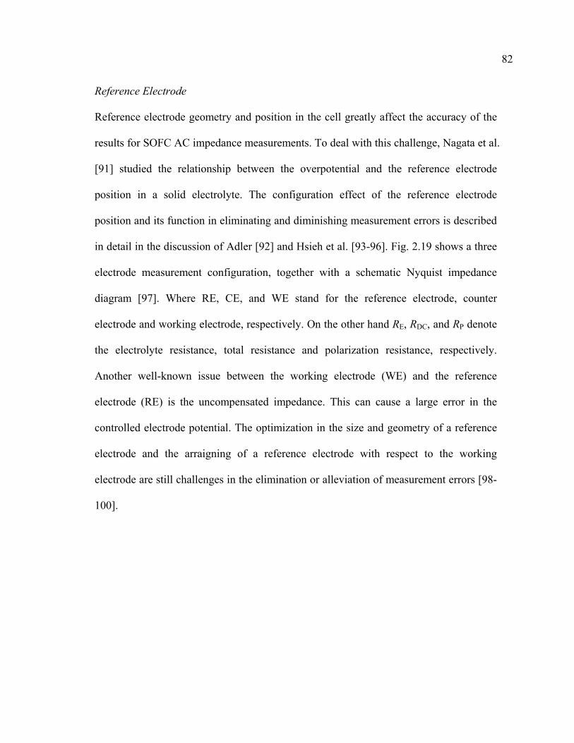
82
Reference Electrode
Reference electrode geometry and position in the cell greatly affect the accuracy of the
results for SOFC AC impedance measurements. To deal with this challenge, Nagata et al.
[91] studied the relationship between the overpotential and the reference electrode
position in a solid electrolyte. The configuration effect of the reference electrode
position and its function in eliminating and diminishing measurement errors is described
in detail in the discussion of Adler [92] and Hsieh et al. [93-96]. Fig. 2.19 shows a three
electrode measurement configuration, together with a schematic Nyquist impedance
diagram [97]. Where RE, CE, and WE stand for the reference electrode, counter
electrode and working electrode, respectively. On the other hand RE, RDC, and RP denote
the electrolyte resistance, total resistance and polarization resistance, respectively.
Another well-known issue between the working electrode (WE) and the reference
electrode (RE) is the uncompensated impedance. This can cause a large error in the
controlled electrode potential. The optimization in the size and geometry of a reference
electrode and the arraigning of a reference electrode with respect to the working
electrode are still challenges in the elimination or alleviation of measurement errors [98-
100].
83
Fig.2.19. Three-electrode measurement configuration and a schematic Nyquist
impedance diagram
Signal-to-Noise Ratio
Because the AC impedance measurement is a very noise sensitive process to facilitate
obtaining reliable data a reasonably high signal-to-noise ratio is required and shielding
and grounding is one of the most popular methods to reduce noise. To monitor noise
level an oscilloscope is often connected to the SOFC current collectors [68]. In addition,
the approach for electric wiring between the fuel cell and the impedance measurement
instruments should deal with different measurement situations and noise reduction,
although the measurement itself is implemented automatically. Calibration using a pre-
constructed equivalent circuit, which has similar AC impedance values to the actual fuel
cell, is essential for measurement validation.
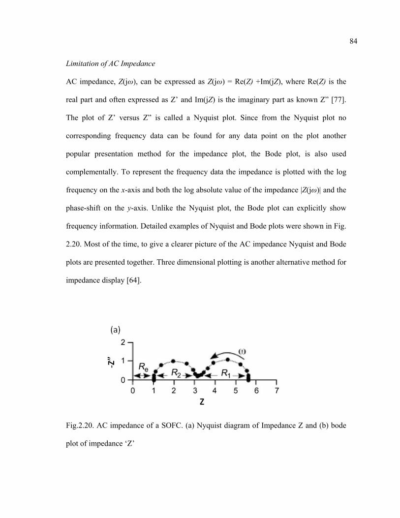
84
Limitation of AC Impedance
AC impedance, Z(jω), can be expressed as Z(jω) = Re(Z) +Im(jZ), where Re(Z) is the
real part and often expressed as Z’ and Im(jZ) is the imaginary part as known Z” [77].
The plot of Z’ versus Z” is called a Nyquist plot. Since from the Nyquist plot no
corresponding frequency data can be found for any data point on the plot another
popular presentation method for the impedance plot, the Bode plot, is also used
complementally. To represent the frequency data the impedance is plotted with the log
frequency on the x-axis and both the log absolute value of the impedance |Z(jω)| and the
phase-shift on the y-axis. Unlike the Nyquist plot, the Bode plot can explicitly show
frequency information. Detailed examples of Nyquist and Bode plots were shown in Fig.
2.20. Most of the time, to give a clearer picture of the AC impedance Nyquist and Bode
plots are presented together. Three dimensional plotting is another alternative method for
impedance display [64].
Fig.2.20. AC impedance of a SOFC. (a) Nyquist diagram of Impedance Z and (b) bode
plot of impedance ‘Z’

85
Fig.2.20. Continued,
The variation of many factors and parameters in SOFCs decides the impedance plot
shapes and based on this shpe useful information such as material composition,
microstructure, and electrochemistry of the fuel cell components can be obtained. It is
well known that the electrode microstructures play a significant role in the
electrochemical reaction because the different microstructures of electrodes can result in
different EIS plot shapes. Therefore, if a relationship between microstructure and
electrochemical kinetic parameters can be made well then the information about the
SOFC microstructure properties could be obtained through EIS modeling. However, due
to the lack of a simple correlation between the impedance plot and SOFC properties, it is
86
very difficult to come to a complete agreement on the interpretation of the impedance
data, especially those from the intermediate to high frequency arcs regime [101-103].
AC impedances ‘Z(jω)’ are the averaged results of all electrochemical processes consist
of the internal and external factors of a SOFC system. And it is also true that there is a
possibility a fuel cell could exhibit an identical impedance plot under completely
different internal and/or external factors. Consequently, it is a challenging work to
explain the transport and reaction mechanisms using only impedance plots. Hence,
impedance plots and other analysis techniques must be used all together in order to
obtain more complete and reliable information [104-107].
AC Impedance Advantages in SOFC Diagnosis
For the past three decades the AC impedance technique has been widely used in fuel cell
characterization. In SOFC characterization, the AC impedance technique provides a very
powerful methode to investigate the reaction kinetics and to optimize cell and material
design and fabrication. This electrochemical impedance measurement technique has
major advantages over other methodologies as stated next. It is nondestructive in the
sense that only small amplitude electronic perturbation is applied and the response is
measured [108, 109]. The AC impedance method can be used to study the individual
processes in SOFCs. It can separate a single process from many other processes
concurrently exist. The transport and reaction processes are considered to take place at
the three-phase boundaries in between the electrode and electrolyte layers, where gas,
ionic species, and electronic species come into contact. These processes involve charge-
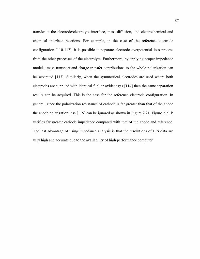
87
transfer at the electrode/electrolyte interface, mass diffusion, and electrochemical and
chemical interface reactions. For example, in the case of the reference electrode
configuration [110-112], it is possible to separate electrode overpotential loss process
from the other processes of the electrolyte. Furthermore, by applying proper impedance
models, mass transport and charge-transfer contributions to the whole polarization can
be separated [113]. Similarly, when the symmetrical electrodes are used where both
electrodes are supplied with identical fuel or oxidant gas [114] then the same separation
results can be acquired. This is the case for the reference electrode configuration. In
general, since the polarization resistance of cathode is far greater than that of the anode
the anode polarization loss [115] can be ignored as shown in Figure 2.21. Figure 2.21 b
verifies far greater cathode impedance compared with that of the anode and reference.
The last advantage of using impedance analysis is that the resolutions of EIS data are
very high and accurate due to the availability of high performance computer.
88
Fig.2.21. (a) Whole cell with a two-electrode configuration and (b) the corresponding
Nyquist plot
89
CHAPTER III
NANOSTRUCTURED CATHODE THIN FILMS WITH VERTICALLY-
ALIGNED NANOPORES FOR THIN FILM SOFC AND THEIR
CHARACTERISTICS*
3.1 Overview
Nanostructured cathode thin films with vertically-aligned nanopores (VANP) were
processed using a pulsed laser deposition technique (PLD). These VANP structures
enhance the oxygen-gas phase diffusivity, thus improve the overall thin film SOFC
performance. La0.5Sr0.5CoO3 (LSCO) and La0.4Sr0.6Co0.8Fe0.2O3 (LSCFO) were deposited
on various substrates (YSZ, Si and pressed Ce0.9Gd0.1O1.95 disks). Microstructures and
properties of the nanostructured cathodes were characterized by TEM, HRTEM, SEM
and electrochemical measurements. Additionally these well aligned VANP structures
relieve or partially relieve the internal thermal stress and lattice strain caused by the
differences of thermal expansion coefficients and lattice mismatch between the electrode
and the electrolyte.
___________ *This chapter is reprinted with permission from “Nanostructured Cathode Thin Films with
Vertically Aligned Nanopores for Thin Film SOFC and Their Characteristics” by J. Yoon, R.Araujo, N Grunbaum, L. Baque´, A Serques, A. Caneiro, X. Zhang, H. Wang, Appl. Surf. Sci. 254 (1) (2007) 266-269. Copyright 2007 by Elsevier.
90
3.2 Introduction
Thin film solid oxide fuel cells (SOFCs) have attracted world-wide research interest for
compact and high-efficiency stationary power applications since they have potentially
high energy-density but high operating temperature. Recent research efforts have been
focused on decreasing the SOFC operating temperature and increasing cell performance
[116,117], which may allow mobile power applications. To achieve the goal of
processing high performance fuel cells operating in the temperature range of 550 °C ≤ T
750 °C, many new materials have been explored for the electrolyte and electrode. For
example, Gadolinia-doped ceria Ce0.9Gd0.1O1.95 (CGO) is one of the best candidates for
the electrolyte to replace Yttria stabilized Zirconia (YSZ) [116-118]; La0.5Sr0.5 3
(LSCO) and La1-xSrxCo0.8Fe0.2O3 (LSCFO) are considered to be promising cathode
terials because of their high electronic (
≥
m
CoO
a eσ ) and ionic ( iσ ) conductivities [119,120],
high oxygen permeability, good catal mpatibility with
CGO. It was reported that the material characteristics including grain size, su
rphology, porosity, path tortuosity, m rial composition and defects play
portant role on the properties of the cathode layer and the kinetics of the oxygen
reduction reactions taking place at the cathode. For exam e, the ionic conductivity
ytic power [
a
121], and excellent co
pl
rface
m
im
o te an
iσ
increases with the Sr and Co compositions in LSCO and LSCFO at the cost of chemical
stability. However, increasing Sr and Co contents increases the thermal expansion
coefficient of the cathode layer and therefore leads to higher thermal mismatch between
the electrolyte (CGO) and cathode layers [122]. To increase the ionic conductivity of the
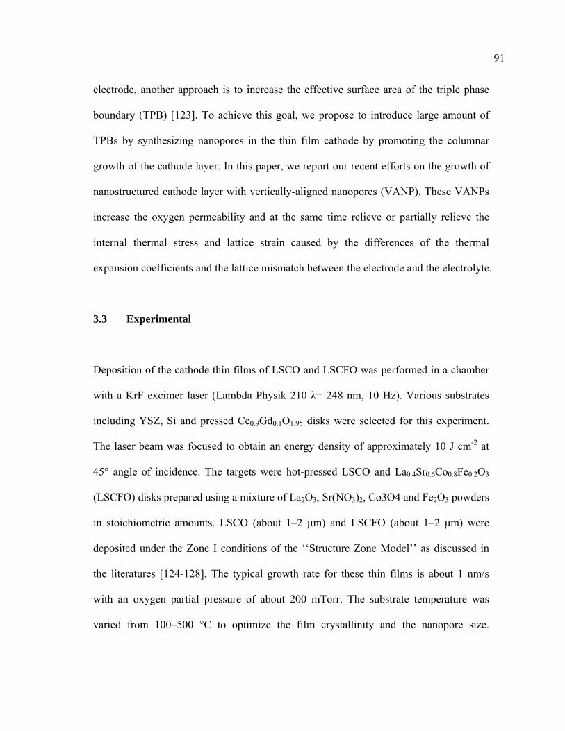
91
electrode, another approach is to increase the effective surface area of the triple phase
boundary (TPB) [123]. To achieve this goal, we propose to introduce large amount of
TPBs by synthesizing nanopores in the thin film cathode by promoting the columnar
growth of the cathode layer. In this paper, we report our recent efforts on the growth of
nanostructured cathode layer with vertically-aligned nanopores (VANP). These VANPs
increase the oxygen permeability and at the same time relieve or partially relieve the
internal thermal stress and lattice strain caused by the differences of the thermal
expansion coefficients and the lattice mismatch between the electrode and the electrolyte.
3.3 Experimental
Deposition of the cathode thin films of LSCO and LSCFO was performed in a chamber
with a KrF excimer laser (Lambda Physik 210 λ= 248 nm, 10 Hz). Various substrates
including YSZ, Si and pressed Ce0.9Gd0.1O1.95 disks were selected for this experiment.
The laser beam was focused to obtain an energy density of approximately 10 J cm-2 at
45° angle of incidence. The targets were hot-pressed LSCO and La0.4Sr0.6Co0.8Fe0.2O3
(LSCFO) disks prepared using a mixture of La2O3, Sr(NO3)2, Co3O4 and Fe2O3 powders
in stoichiometric amounts. LSCO (about 1–2 μm) and LSCFO (about 1–2 μm) were
deposited under the Zone I conditions of the ‘‘Structure Zone Model’’ as discussed in
the literatures [124-128]. The typical growth rate for these thin films is about 1 nm/s
with an oxygen partial pressure of about 200 mTorr. The substrate temperature was
varied from 100–500 °C to optimize the film crystallinity and the nanopore size.
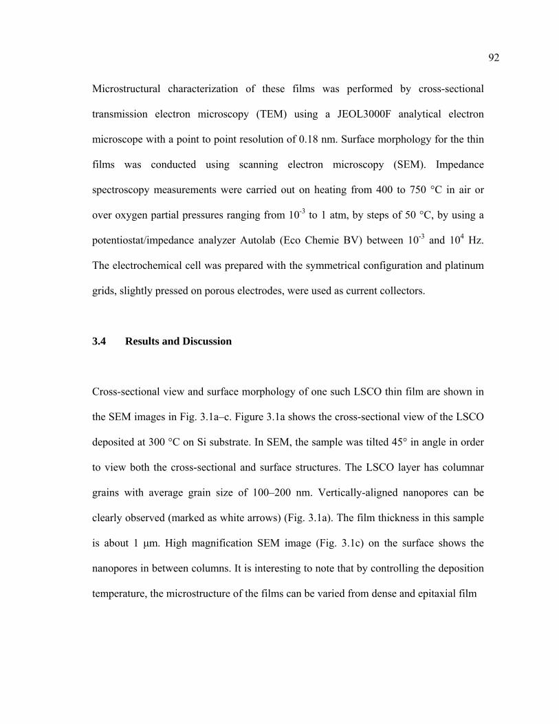
92
Microstructural characterization of these films was performed by cross-sectional
transmission electron microscopy (TEM) using a JEOL3000F analytical electron
microscope with a point to point resolution of 0.18 nm. Surface morphology for the thin
films was conducted using scanning electron microscopy (SEM). Impedance
spectroscopy measurements were carried out on heating from 400 to 750 °C in air or
over oxygen partial pressures ranging from 10-3 to 1 atm, by steps of 50 °C, by using a
potentiostat/impedance analyzer Autolab (Eco Chemie BV) between 10-3 and 104 Hz.
The electrochemical cell was prepared with the symmetrical configuration and platinum
grids, slightly pressed on porous electrodes, were used as current collectors.
3.4 Results and Discussion
Cross-sectional view and surface morphology of one such LSCO thin film are shown in
the SEM images in Fig. 3.1a–c. Figure 3.1a shows the cross-sectional view of the LSCO
deposited at 300 °C on Si substrate. In SEM, the sample was tilted 45° in angle in order
to view both the cross-sectional and surface structures. The LSCO layer has columnar
grains with average grain size of 100–200 nm. Vertically-aligned nanopores can be
clearly observed (marked as white arrows) (Fig. 3.1a). The film thickness in this sample
is about 1 μm. High magnification SEM image (Fig. 3.1c) on the surface shows the
nanopores in between columns. It is interesting to note that by controlling the deposition
temperature, the microstructure of the films can be varied from dense and epitaxial film
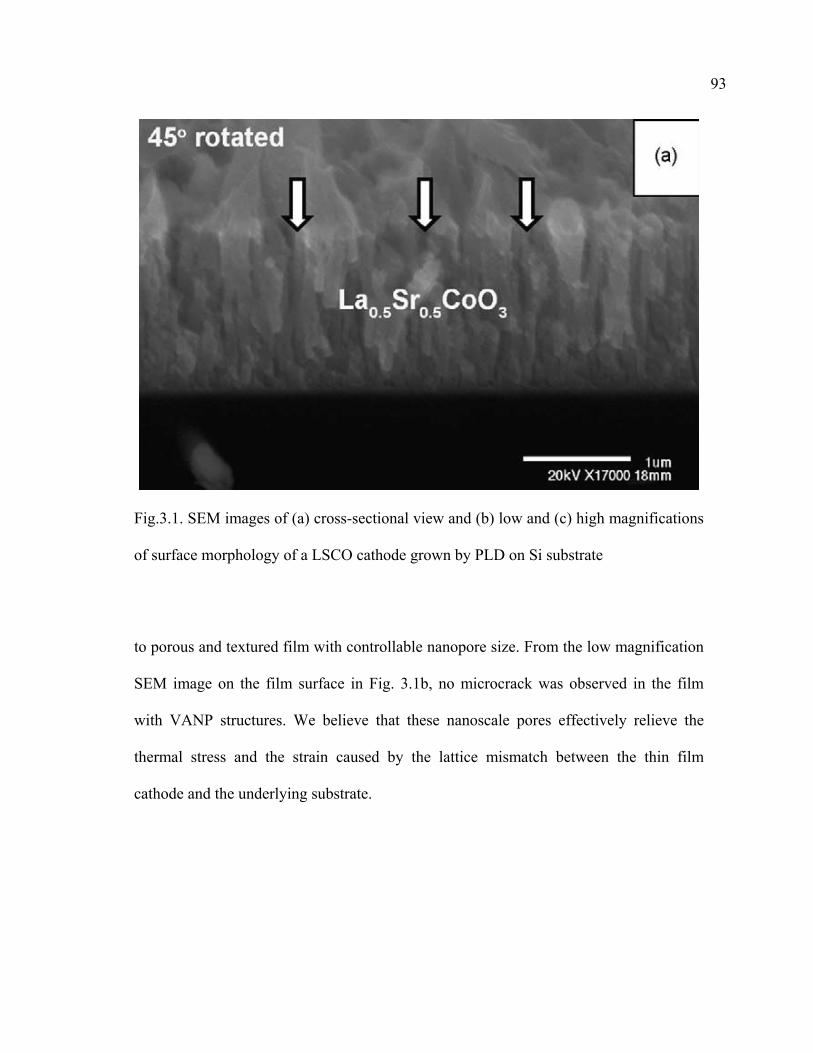
93
Fig.3.1. SEM images of (a) cross-sectional view and (b) low and (c) high magnifications
of surface morphology of a LSCO cathode grown by PLD on Si substrate
to porous and textured film with controllable nanopore size. From the low magnification
SEM image on the film surface in Fig. 3.1b, no microcrack was observed in the film
with VANP structures. We believe that these nanoscale pores effectively relieve the
thermal stress and the strain caused by the lattice mismatch between the thin film
cathode and the underlying substrate.
94
Fig.3.1. Continued,
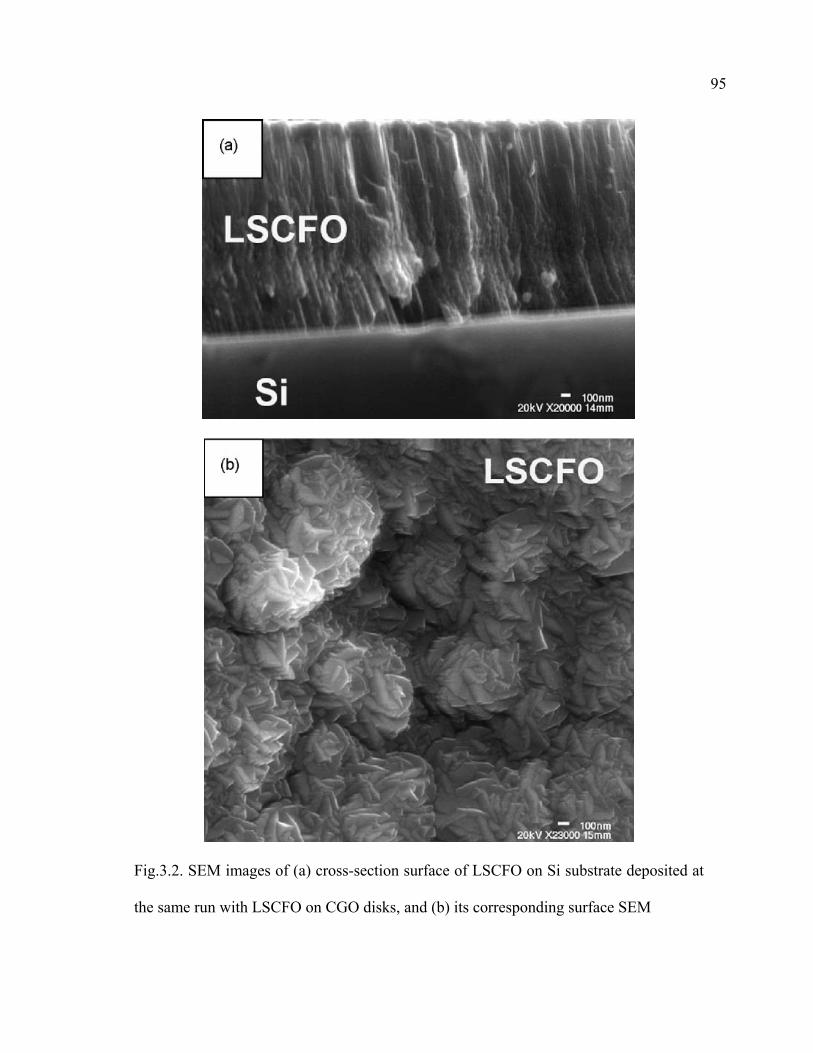
95
Fig.3.2. SEM images of (a) cross-section surface of LSCFO on Si substrate deposited at
the same run with LSCFO on CGO disks, and (b) its corresponding surface SEM
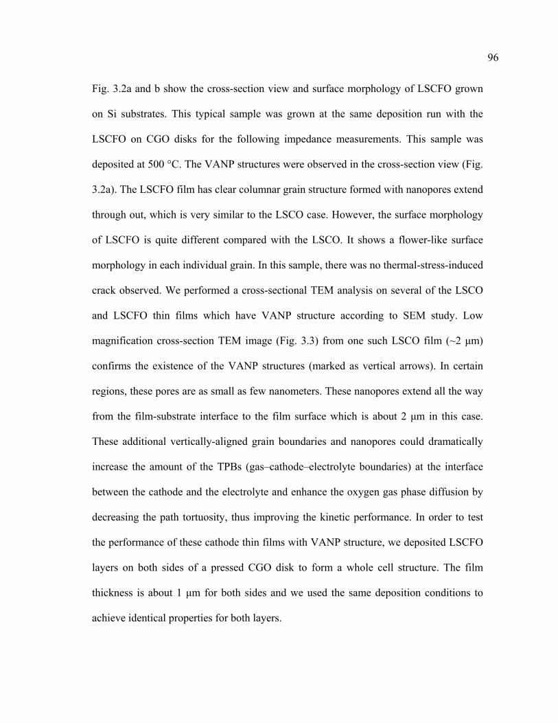
96
Fig. 3.2a and b show the cross-section view and surface morphology of LSCFO grown
on Si substrates. This typical sample was grown at the same deposition run with the
LSCFO on CGO disks for the following impedance measurements. This sample was
deposited at 500 °C. The VANP structures were observed in the cross-section view (Fig.
3.2a). The LSCFO film has clear columnar grain structure formed with nanopores extend
through out, which is very similar to the LSCO case. However, the surface morphology
of LSCFO is quite different compared with the LSCO. It shows a flower-like surface
morphology in each individual grain. In this sample, there was no thermal-stress-induced
crack observed. We performed a cross-sectional TEM analysis on several of the LSCO
and LSCFO thin films which have VANP structure according to SEM study. Low
magnification cross-section TEM image (Fig. 3.3) from one such LSCO film (~2 μm)
confirms the existence of the VANP structures (marked as vertical arrows). In certain
regions, these pores are as small as few nanometers. These nanopores extend all the way
from the film-substrate interface to the film surface which is about 2 μm in this case.
These additional vertically-aligned grain boundaries and nanopores could dramatically
increase the amount of the TPBs (gas–cathode–electrolyte boundaries) at the interface
between the cathode and the electrolyte and enhance the oxygen gas phase diffusion by
decreasing the path tortuosity, thus improving the kinetic performance. In order to test
the performance of these cathode thin films with VANP structure, we deposited LSCFO
layers on both sides of a pressed CGO disk to form a whole cell structure. The film
thickness is about 1 μm for both sides and we used the same deposition conditions to
achieve identical properties for both layers.
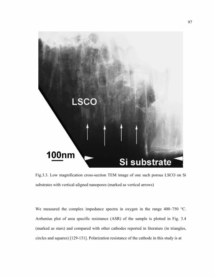
97
Fig.3.3. Low magnification cross-section TEM image of one such porous LSCO on Si
substrates with vertical-aligned nanopores (marked as vertical arrows)
We measured the complex impedance spectra in oxygen in the range 400–750 °C.
Arrhenius plot of area specific resistance (ASR) of the sample is plotted in Fig. 3.4
(marked as stars) and compared with other cathodes reported in literature (in triangles,
circles and squares) [129-131]. Polarization resistance of the cathode in this study is at
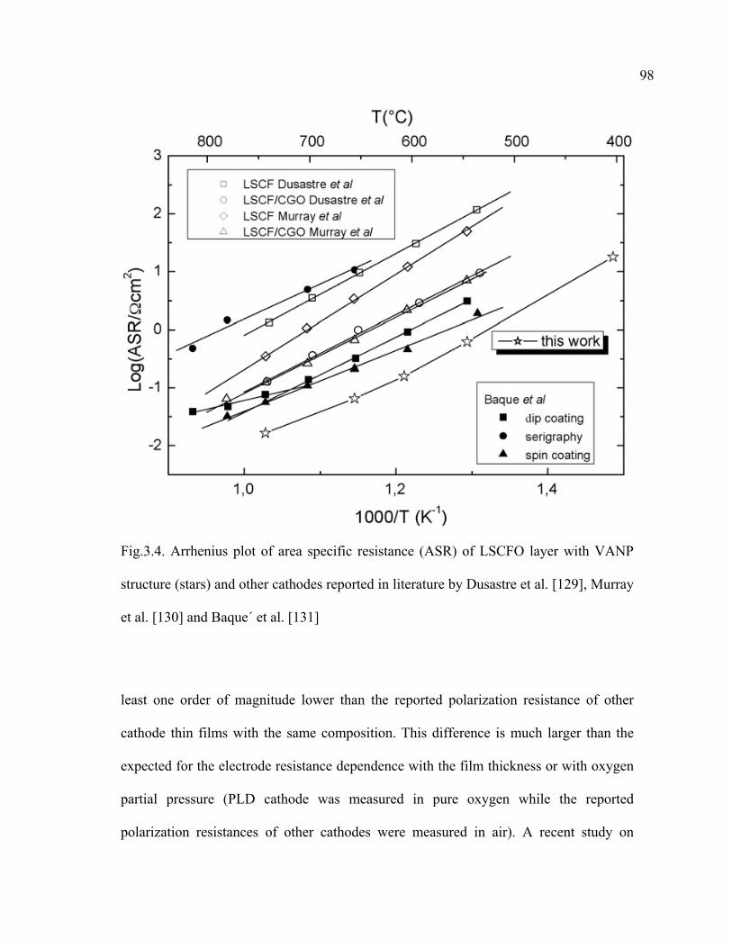
98
Fig.3.4. Arrhenius plot of area specific resistance (ASR) of LSCFO layer with VANP
structure (stars) and other cathodes reported in literature by Dusastre et al. [129], Murray
et al. [130] and Baque´ et al. [131]
least one order of magnitude lower than the reported polarization resistance of other
cathode thin films with the same composition. This difference is much larger than the
expected for the electrode resistance dependence with the film thickness or with oxygen
partial pressure (PLD cathode was measured in pure oxygen while the reported
polarization resistances of other cathodes were measured in air). A recent study on
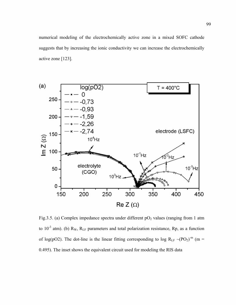
99
numerical modeling of the electrochemically active zone in a mixed SOFC cathode
suggests that by increasing the ionic conductivity we can increase the electrochemically
active zone [123].
Fig.3.5. (a) Complex impedance spectra under different pO2 values (ranging from 1 atm
to 10-3 atm). (b) RW, RLF parameters and total polarization resistance, Rp, as a function
of log(pO2). The dot-line is the linear fitting corresponding to log RLF ~(PO2)-m (m =
0.495). The inset shows the equivalent circuit used for modeling the RIS data
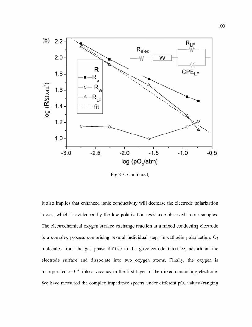
100
Fig.3.5. Continued,
It also implies that enhanced ionic conductivity will decrease the electrode polarization
losses, which is evidenced by the low polarization resistance observed in our samples.
The electrochemical oxygen surface exchange reaction at a mixed conducting electrode
is a complex process comprising several individual steps in cathodic polarization, O2
molecules from the gas phase diffuse to the gas/electrode interface, adsorb on the
electrode surface and dissociate into two oxygen atoms. Finally, the oxygen is
incorporated as O2- into a vacancy in the first layer of the mixed conducting electrode.
We have measured the complex impedance spectra under different pO2 values (ranging
101
from 1 atm to 10-3 atm) at 400 °C to determine which of these processes is limiting the
electrode reaction (shown in Fig. 3.5a). Using an equivalent circuit (insert in Fig. 3.5b)
[132]. We found that the low frequency resistance fits the usual form log RLF ~ (PO2)-m
with m ~ 0.5, expected for a dissociative surface-adsorption limited behavior, whereas
according to some models, m = 1 is expected for an oxygen diffusion limited mechanism
[133-134]. This indicates that a significant portion of the electrode surface is active for
oxygen reduction. Impedance measurements for various nanopore size and densities
samples are in progress to further understand this complex process.
3.5 Summary
We have successfully processed nanostructured LSCO and LSCFO cathode thin films
for thin film SOFC. All the films grow as columnar grains, which leaves nanopores in
between the grains. The unique VANP structures in these cathode thin films penetrate
throughout the film thickness as deep as 2 μm and produce enhanced oxygen
conductance in the cathode layer. Additionally impedance measurements demonstrate
that the cathode thin films with VANPs have low polarization resistance values and
enhanced kinetic performance in the low temperature regime (400–700 °C).
102
CHAPTER IV
VERTICALLY ALIGNED NANOCOMPOSITE THIN FILM AS
CATHODE ELECTROLYTE INTERFACE LAYER FOR THIN FILM
SOLID OXIDE FUEL
4.1 Overview
A thin layer of vertically-aligned nanocomposite (VAN) structure was deposited in
between the electrolyte Ce0.9Gd0.1O1.95 (CGO), and the thin film cathode layer
La0.5Sr0.5CoO3 (LSCO) for thin film solid oxide fuel cells (SOFCs). The VAN structure
consists of the electrolyte and the cathode materials in the composition of (CGO) 0.5
(LSCO) 0.5. The self-assembled VAN nanostructures contain highly ordered alternating
vertical columns formed through a one-step thin film deposition using a pulsed laser
deposition technique (PLD). These VAN structures significantly increase the interface
area between the electrolyte and the cathode as well as the area of active triple phase
boundary (TPB), thus improve the overall thin film SOFC performance at low
temperatures, as low as 400oC, demonstrated by electrochemical impedance
spectroscopy measurements. In addition, the binary VAN interlayer could act as the
transition layer that improve the adhesion and relieve the thermal stress and lattice strain
between the cathode and the electrolyte.
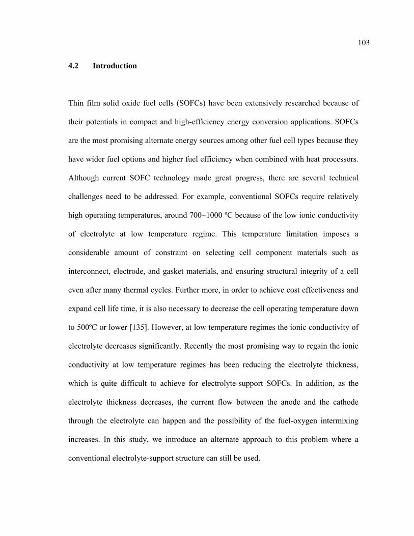
103
4.2 Introduction
Thin film solid oxide fuel cells (SOFCs) have been extensively researched because of
their potentials in compact and high-efficiency energy conversion applications. SOFCs
are the most promising alternate energy sources among other fuel cell types because they
have wider fuel options and higher fuel efficiency when combined with heat processors.
Although current SOFC technology made great progress, there are several technical
challenges need to be addressed. For example, conventional SOFCs require relatively
high operating temperatures, around 700~1000 ºC because of the low ionic conductivity
of electrolyte at low temperature regime. This temperature limitation imposes a
considerable amount of constraint on selecting cell component materials such as
interconnect, electrode, and gasket materials, and ensuring structural integrity of a cell
even after many thermal cycles. Further more, in order to achieve cost effectiveness and
expand cell life time, it is also necessary to decrease the cell operating temperature down
to 500ºC or lower [135]. However, at low temperature regimes the ionic conductivity of
electrolyte decreases significantly. Recently the most promising way to regain the ionic
conductivity at low temperature regimes has been reducing the electrolyte thickness,
which is quite difficult to achieve for electrolyte-support SOFCs. In addition, as the
electrolyte thickness decreases, the current flow between the anode and the cathode
through the electrolyte can happen and the possibility of the fuel-oxygen intermixing
increases. In this study, we introduce an alternate approach to this problem where a
conventional electrolyte-support structure can still be used.
104
In this paper, a vertically aligned nanocomposite (VAN) layer in between the cathode
and the electrolyte was intentionally built to effectively reduce the polarization
resistance at the cathode/electrolyte interface. It was previously reported that the
microstructural variations in the electrolyte and the electrode could affect the reaction
kinetics of thin film SOFCs dramatically [136-141] and the main part of power losses in
planar SOFCs occurs as a result of the polarization resistance at the cathode/electrolyte
interface. The binary VAN interlayer is a composite of cathode and electrolyte materials,
in our case, La0.5Sr0.5CoO3 (LSCO) and Ce0.9Gd0.1O1.95 (CGO). It is processed through
a single step deposition without any additional lithography patterning steps. A schematic
sketch of the binary VAN interlayer is given in Fig. 4.1a and b. This layer effectively
increases the cathode-electrolyte interface area in a controllable way, and thus lowers the
polarization resistance of the cathode/electrolyte interface and improves the kinetic
performance of the cathode. These all lead to the improvement in the overall thin film
SOFCs performance.
105
Fig.4.1. (a) Schematic diagram of a symmetric cell and (b) VAN interlayer where “L”
and “C” stand for LSCO and CGO columns, respectively
4.3 Experimental
Pulsed laser depositions (PLD) of the LSCO/CGO VAN interlayer and the following
LSCO cathode layer were performed in a multitarget chamber with a KrF excimer laser
(Lambda Physik 210, λ = 248 nm, 5-10 Hz). Various substrates including Yttria-
stabilized Zirconia (YSZ), SrTiO3 (STO) and pressed CGO disks were selected for this
work. The laser beam was focused to obtain an energy density of approximately 10J cm-2
at 45º angle of incidence. The hot-pressed targets including LSCO and LSCO+CGO
(50:50), and CGO electrolyte disks were all prepared by mixing the stoichiometric
amounts of powders including La2O3, Sr(NO3)2, Co3O4, CeO2 and Gd2O3. LSCO/CGO
VAN interlayers (about 50–100 nm) were processed through one-step thin film
106
deposition. Subsequent LSCO thin film cathode layer with vertically aligned nanopores
(about 500nm) (VANP) was deposited under the condition stated in our previous work
[142]. The growth rate for these thin films was controlled at about 1 nm/s for LSCO
cathode layer and 0.1 nm/s for LSCO/CGO VAN interlayer at an oxygen partial pressure
of about 200 mTorr. The substrate temperature was varied from 300–700 ºC to optimize
the film crystallinity and the nanopore size of the cathode layer. Four symmetrical
working cells with different VAN thicknesses were prepared to study the effects of
interlayer thickness on cell performance. Microstructural characterizations of these films
were performed by cross-sectional transmission electron microscopy (TEM) using a
JEOL2010 analytical electron microscope and a JEOL3000F analytical electron
microscope with a point to point resolution of 0.18 nm. Scanning transmission electron
microscopy (STEM) was performed by a FEI Tecnai F20 with a point to point resolution
of 0.27nm. Surface morphology study for the thin films was conducted by scanning
electron microscopy (SEM). Impedance spectroscopy measurements were carried out on
heating from 400 to 600 ºC in pure oxygen by steps of 50 ºC, by using a
potentiostat/impedance analyzer Autolab (Eco Chemie BV) between 10-3 and 106 Hz.
Each temperature was measured after 3-8 hours waiting until the system was stable. The
electrochemical cells were prepared with the symmetrical configuration and platinum
grids, slightly pressed on porous electrodes, were used as current collectors.
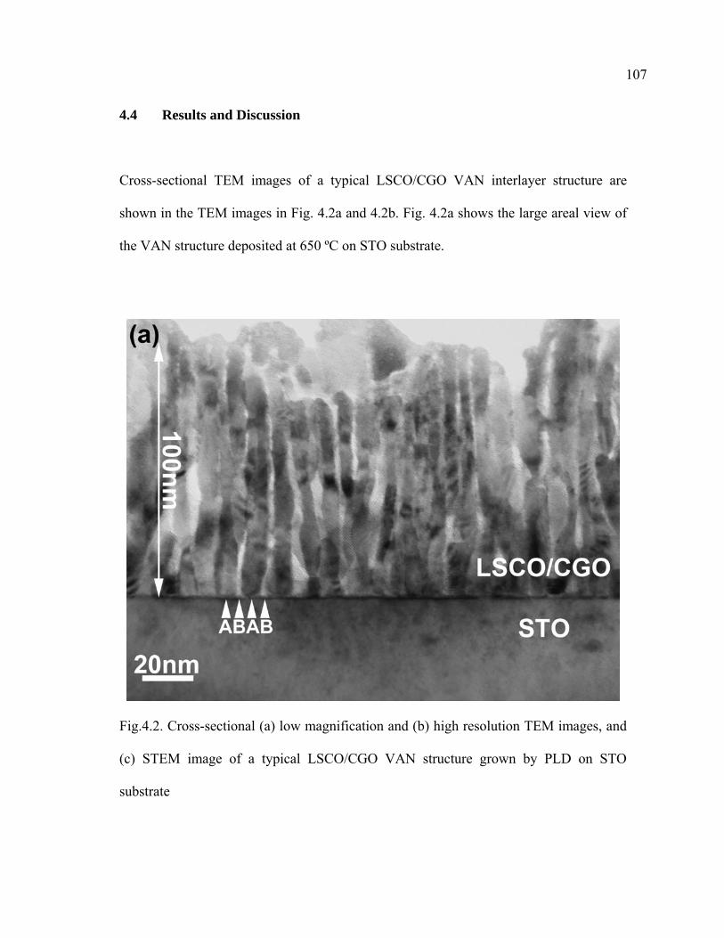
107
4.4 Results and Discussion
Cross-sectional TEM images of a typical LSCO/CGO VAN interlayer structure are
shown in the TEM images in Fig. 4.2a and 4.2b. Fig. 4.2a shows the large areal view of
the VAN structure deposited at 650 ºC on STO substrate.
Fig.4.2. Cross-sectional (a) low magnification and (b) high resolution TEM images, and
(c) STEM image of a typical LSCO/CGO VAN structure grown by PLD on STO
substrate
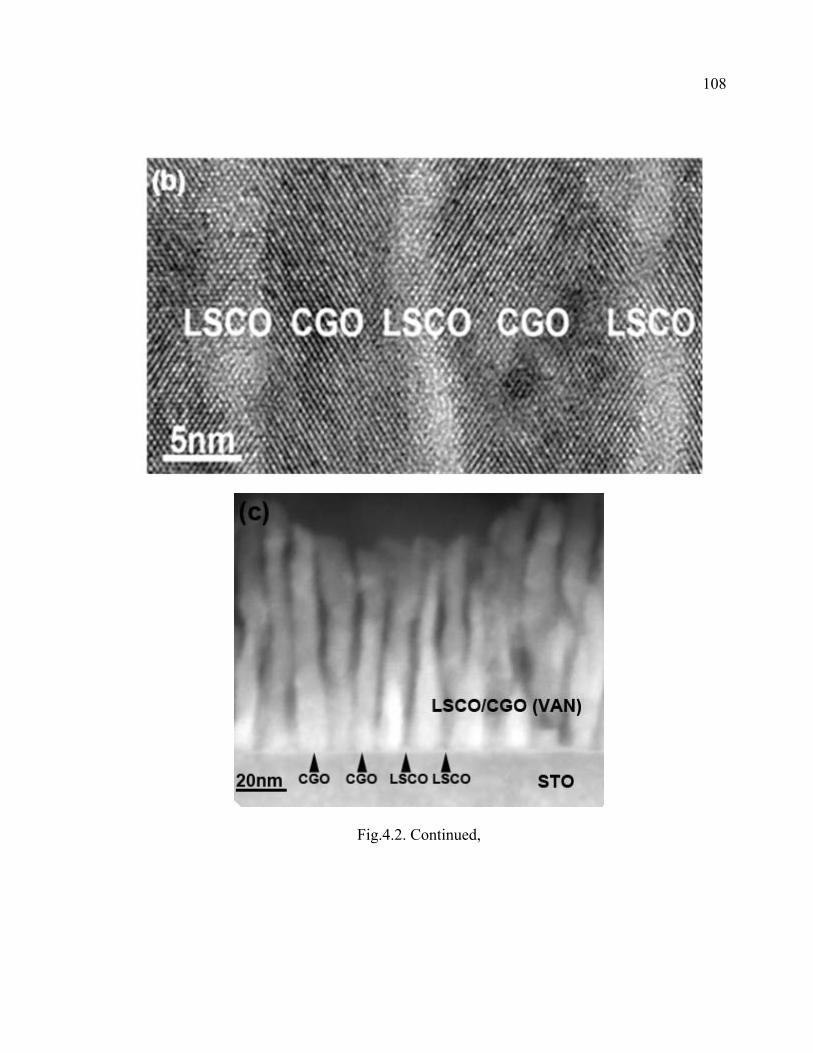
108
Fig.4.2. Continued,
109
It is clear that CGO and LSCO grains grow as alternating vertically aligned columns
over a large area. Each of the columns is around 10 nm in diameter. The VAN structure
extends all the way through the film thickness, in this case, 100 nm. The reason that we
chose single crystal YSZ and STO substrates first to grow the VAN structure is to
demonstrate the growth of the binary VAN structures of LSCO/CGO. LSCO has a
perovskite structure with a lattice parameter of 0.381 nm and CGO is face-centered
cubic with a lattice parameter of 1.084 nm (2 × 0.542 nm). Both of them match well with
YSZ (a= 0.515 nm) and STO (a=0.390 nm), either through direct cube-on-cube
matching or after 45o rotation. Another important consideration is that the possibility of
intermixing between LSCO and CGO is rather small as their cations are rather big and
the interstitial sites are relatively small. Previously we have successfully demonstrated
the growth of BiFeO3 / Sm2O3 VAN structure on STO substrate and LSMO/ZnO VAN
structure on sapphire with similar materials selection criteria [143-145]. A high
resolution TEM image covering a set of VAN columns is shown in Fig. 4.2b.
LSCO/CGO binary VAN structure can be clearly observed (labeled as LSCO and CGO)
based on their contrast difference.
To confirm that LSCO and CGO grow as alternative columns without intermixing, we
conducted STEM study under the high angle annular dark field (HAADF) condition.
This is also called Z-contrast, where the contrast is roughly proportional to Z2 (more
accurately, Z1.7 ). A typical Z-contrast image over a large area of the LSCO/CGO VAN
structure is shown as Fig. 4.2c. Because of higher Z numbers of Ce and Ga, CGO
110
columns have much higher contrast (brighter columns) than LSCO columns. The CGO
and LSCO columns are clearly vertically aligned and alternating with each other with an
average column size of 5-10 nm. The vertical column interfaces are sharp and clean. We
also conducted a detailed EDX mapping over the same area (not shown here) and no
obvious intermixing was detected under the EDX detecting sensitivity.
In order to measure the electrochemical characteristics and test the performance of the
cathode structure with the VAN interlayer, we processed the symmetric cells with the
VAN interlayer deposited on both sides of a pressed CGO disk followed by depositing
thin film cathode with VANP as illustrated in Fig.4.1. The total cathode thickness is
about 600 nm on both sides. We used the same deposition conditions to ensure the
identical properties for both sides of the cells. Four button cells with different VAN
interlayer thicknesses were prepared in order to investigate the relationship between the
VAN thickness and the electrochemical performance of the cells. The VAN structure can
effectively increase the cathode-electrolyte interface area in a controllable way. The
information on the VAN film thickness and the ratio between the interface area densities
with and without the VAN layer is summarized in Table 4.1. For example, the 100nm-
thick VAN structure can increase the interface area 25 times compared with the case
without the VAN interlayer. By controlling the interlayer thickness, one can
systematically vary the interface area density. For this typical VAN structure, the
average width of these nano-columns are about 5~10 nm. It is interesting to note that by
controlling the deposition conditions such as temperature and the stoichiometry of the
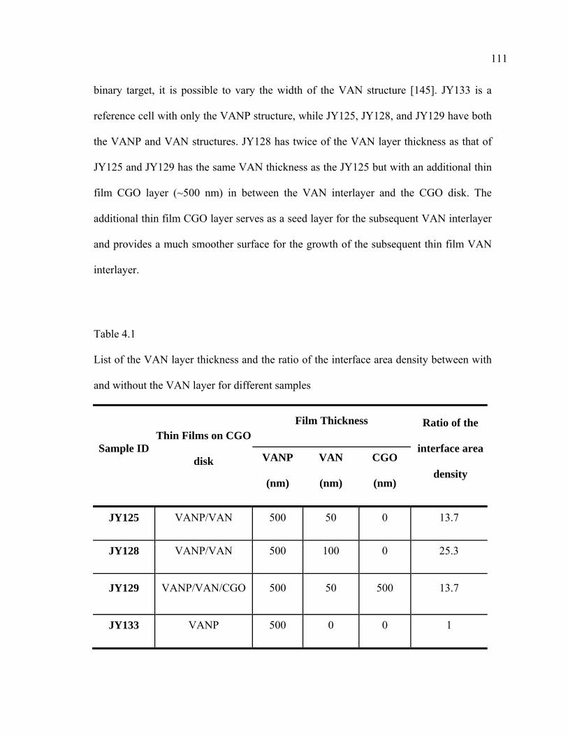
111
binary target, it is possible to vary the width of the VAN structure [145]. JY133 is a
reference cell with only the VANP structure, while JY125, JY128, and JY129 have both
the VANP and VAN structures. JY128 has twice of the VAN layer thickness as that of
JY125 and JY129 has the same VAN thickness as the JY125 but with an additional thin
film CGO layer (~500 nm) in between the VAN interlayer and the CGO disk. The
additional thin film CGO layer serves as a seed layer for the subsequent VAN interlayer
and provides a much smoother surface for the growth of the subsequent thin film VAN
interlayer.
Table 4.1
List of the VAN layer thickness and the ratio of the interface area density between with
and without the VAN layer for different samples
Sample ID Thin Films on CGO
disk
Film Thickness Ratio of the
interface area
density VANP
(nm)
VAN
(nm)
CGO
(nm)
JY125 VANP/VAN 500 50 0 13.7
JY128 VANP/VAN 500 100 0 25.3
JY129 VANP/VAN/CGO 500 50 500 13.7
JY133 VANP 500 0 0 1
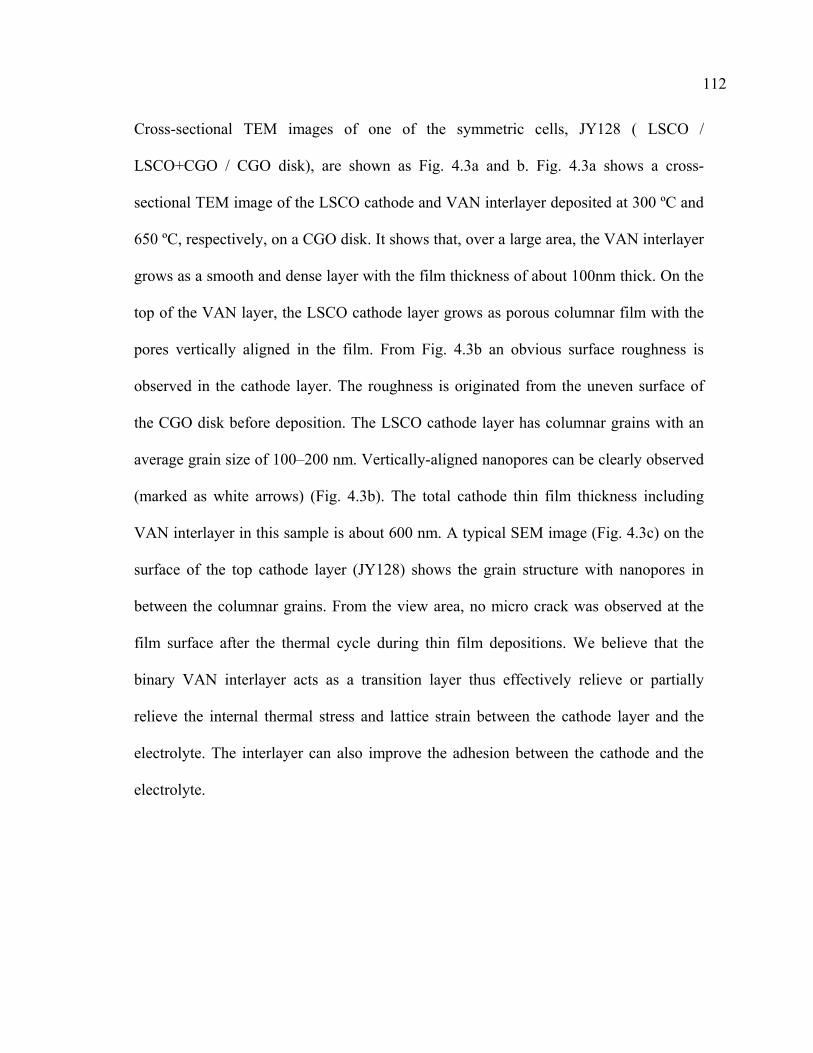
112
Cross-sectional TEM images of one of the symmetric cells, JY128 ( LSCO /
LSCO+CGO / CGO disk), are shown as Fig. 4.3a and b. Fig. 4.3a shows a cross-
sectional TEM image of the LSCO cathode and VAN interlayer deposited at 300 ºC and
650 ºC, respectively, on a CGO disk. It shows that, over a large area, the VAN interlayer
grows as a smooth and dense layer with the film thickness of about 100nm thick. On the
top of the VAN layer, the LSCO cathode layer grows as porous columnar film with the
pores vertically aligned in the film. From Fig. 4.3b an obvious surface roughness is
observed in the cathode layer. The roughness is originated from the uneven surface of
the CGO disk before deposition. The LSCO cathode layer has columnar grains with an
average grain size of 100–200 nm. Vertically-aligned nanopores can be clearly observed
(marked as white arrows) (Fig. 4.3b). The total cathode thin film thickness including
VAN interlayer in this sample is about 600 nm. A typical SEM image (Fig. 4.3c) on the
surface of the top cathode layer (JY128) shows the grain structure with nanopores in
between the columnar grains. From the view area, no micro crack was observed at the
film surface after the thermal cycle during thin film depositions. We believe that the
binary VAN interlayer acts as a transition layer thus effectively relieve or partially
relieve the internal thermal stress and lattice strain between the cathode layer and the
electrolyte. The interlayer can also improve the adhesion between the cathode and the
electrolyte.
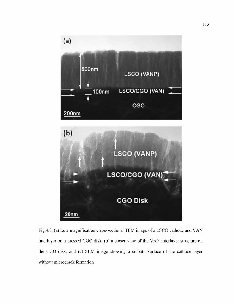
113
Fig.4.3. (a) Low magnification cross-sectional TEM image of a LSCO cathode and VAN
interlayer on a pressed CGO disk, (b) a closer view of the VAN interlayer structure on
the CGO disk, and (c) SEM image showing a smooth surface of the cathode layer
without microcrack formation
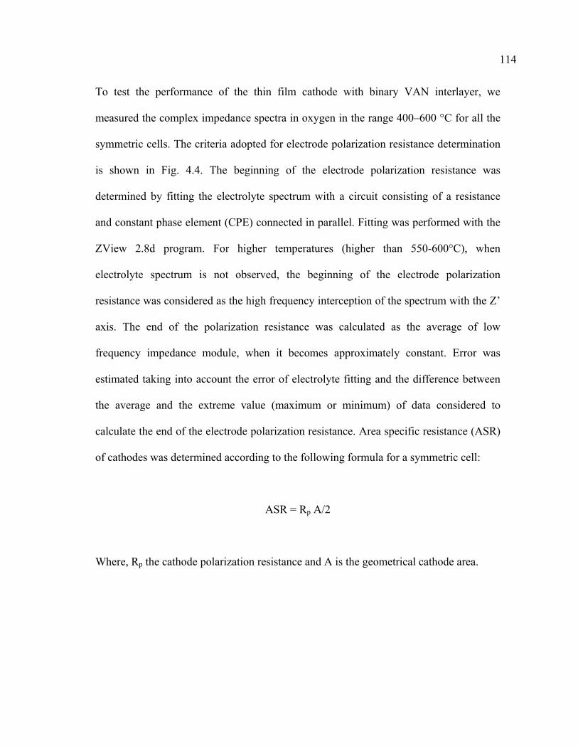
114
To test the performance of the thin film cathode with binary VAN interlayer, we
measured the complex impedance spectra in oxygen in the range 400–600 °C for all the
symmetric cells. The criteria adopted for electrode polarization resistance determination
is shown in Fig. 4.4. The beginning of the electrode polarization resistance was
determined by fitting the electrolyte spectrum with a circuit consisting of a resistance
and constant phase element (CPE) connected in parallel. Fitting was performed with the
ZView 2.8d program. For higher temperatures (higher than 550-600°C), when
electrolyte spectrum is not observed, the beginning of the electrode polarization
resistance was considered as the high frequency interception of the spectrum with the Z’
axis. The end of the polarization resistance was calculated as the average of low
frequency impedance module, when it becomes approximately constant. Error was
estimated taking into account the error of electrolyte fitting and the difference between
the average and the extreme value (maximum or minimum) of data considered to
calculate the end of the electrode polarization resistance. Area specific resistance (ASR)
of cathodes was determined according to the following formula for a symmetric cell:
ASR = Rp A/2
Where, Rp the cathode polarization resistance and A is the geometrical cathode area.
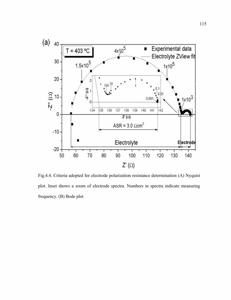
115
Fig.4.4. Criteria adopted for electrode polarization resistance determination (A) Nyquist
plot. Inset shows a zoom of electrode spectra. Numbers in spectra indicate measuring
frequency. (B) Bode plot
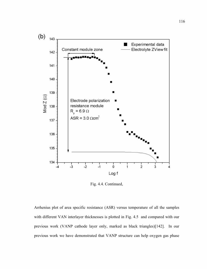
116
Fig. 4.4. Continued,
Arrhenius plot of area specific resistance (ASR) versus temperature of all the samples
with different VAN interlayer thicknesses is plotted in Fig. 4.5 and compared with our
previous work (VANP cathode layer only, marked as black triangles)[142]. In our
previous work we have demonstrated that VANP structure can help oxygen gas phase
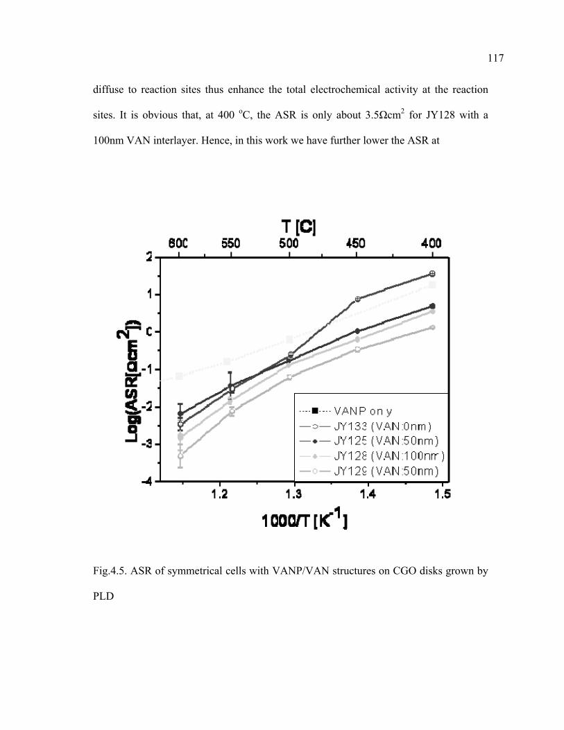
117
diffuse to reaction sites thus enhance the total electrochemical activity at the reaction
sites. It is obvious that, at 400 oC, the ASR is only about 3.5Ωcm2 for JY128 with a
100nm VAN interlayer. Hence, in this work we have further lower the ASR at
Fig.4.5. ASR of symmetrical cells with VANP/VAN structures on CGO disks grown by
PLD
118
least one order of magnitude than our previous work by including the binary VAN
interlayers. Data measured above 550 °C have a big error due to the small resistance.
Considering the fact that iron or manganese doped LSCO cathodes demonstrate better
performance than simple LSCO cathodes, this work suggests that doped LSCO cathodes
can improve the fuel cell performance even further by inserting the VAN interface layer.
Fig. 4.5 indicates the general trend of ASR as a function of the VAN thickness, i.e., the
ASR plot shifts to lower values as the VAN interlayer thickness increases. This suggests
that the VAN interlayer indeed plays a very important role in the ASR decrease. As
listed in Table 4.1, the cathode / electrolyte interface area density increases as the VAN
interlayer thickness increases. Therefore the VAN interlayer enhances the catalytic
reaction probability of TPBs (gas–cathode–electrolyte boundaries) by increasing the
effective area of the TPBs, and thus decreases the cathode resistance and lowers the
polarization resistance of the cathode/electrolyte interface, which leads to the overall
improved thin film SOFC performance. It is noted that, the results reproduce well at
different temperatures after the high temperature thermal cycles during the measurement.
We can therefore conclude that, there is no significant structural degradation (second
phase formation or interface diffusion) for the cells with the VAN interlayer and the
VAN structure is stable after thermal cycles.
JY129 (with an additional CGO seed layer) shows the lowest ASR, which is about 35%
lower than that of JY125 (no CGO seed layer). This supports the effectiveness of the
additional thin film CGO layer. The possible functions of the CGO seed layer are: (1)
119
improving the gas tightness of hot pressed 0.9mm thick CGO electrolyte, (2) preventing
interface reactions, such as the formation of insulating La-composite at the interface
between electrolytes and cathode materials, and possibly, (3) improving the charge
transfer process at the electrode and the electrolyte interface [146]. The effect of the
CGO layer became more obvious at lower temperature regime than that at the high
temperature regime. This is because that, the grain boundary effects become significant
at the intermediate temperature regime, 400 ºC to 600 ºC, since the grain boundary
region has lower ionic conductivity and higher activation energy than the bulk
lattice[147]. However, at higher operating temperature, above 700 ºC, the grain
boundary effect can be negligible because of high enough temperatures to overcome the
high activation energy.
4.5 Summary
We have successfully processed binary VAN interlayer of (LSCO)0.5 (CGO)0.5 in
between the cathode and electrolyte for high efficiency thin film SOFC. This unique
binary VAN structured interlayer effectively increases the cathode/electrolyte interface
area density (by 14~25 times depending on the interlayer thickness) and thus
significantly lowers the polarization resistance present at the cathode/electrolyte
interface. Hence a low cathode polarization resistance (9x10⁻⁴ Ω at 599oC, 2.39 Ω at
400oC) was achieved at low operation temperatures based on the impedance
measurements at low temperature regime (400~600 ºC). The interface area density can

120
be systematically controlled by varying the VAN interlayer thickness and column width,
which can be achieved through tuning the deposition parameters. As the VAN thickness
increases, the ASR shifts to lower values. By combining a CGO seed layer with the
VAN interlayer, we have demonstrated a record low ASR (4.84 x10⁻⁴ Ωcm2 at 599oC,
1.25 Ωcm2 at 400oC).
121
CHAPTER V
MICROSTRUCTURAL STUDY OF THIN FILM Ce0.90Gd0.10O1.95 (CGO)
AS ELECTOROLYTE FOR SOLID OXIDE FUEL CELL APPLICATIONS
5.1 Overview
The microstructural properties and growth mechanisms of Ce0.90Gd0.10O1.95 (CGO) thin
film as electrolyte prepared by pulsed laser deposition technique were investigated. The
CGO thin films on single crystal Yittria-stabilized Zirconia (YSZ) substrates with the
film thickness from 1.5µm to 6.7µm were prepared. Thin film CGO electrolytes with
different grain sizes and crystal structures were prepared under different deposition
conditions. The effect of the deposition conditions, such as substrate temperature,
oxygen partial pressure, target repetition rate, and laser ablation energy on the
microstructural properties of these films are examined using X-ray diffraction (XRD),
transmission electron microscopy (TEM), scanning electron microscopy (SEM), and
optical microscopy. CGO thin film deposited above 500 ºC starts to show epitaxial
growth on YSZ substrates. The present study suggests that substrate temperature
significantly influences the microstructure of the films especially film grain size.
122
5.2 Introduction
Solid oxide fuel cells (SOFCs) offer an environmentally friendly alternative to
conventional energy conversion devices [148]. A typical SOFC consists of two
electrodes (anode and cathode) separated by an electrolyte. Yttria-stabilized zirconia
(YSZ) is considered to be the most reliable candidate as the electrolyte and has been
widely used. However, for YSZ to acquire sufficiently high oxygen ion conductivity, a
high operating temperature, typically around 1000 ˚C, is required, which severely limits
the component material selections and decrease the long term performance stability of
SOFCs [149]. Therefore, it is necessary to lower the operating temperature from the
traditional 1000 ˚C to an intermediate/low temperature range of 400–700 ˚C. The lower
temperature of application provides a greater flexibility in the choice of electrode and
interconnects materials, reduction in thermal stresses in active ceramic structures, as well
as a longer lifetime of the cells. However, significant barriers to intermediate/low
temperature SOFCs are the increase of electrolyte resistance and high electrode
overpotentials. There have been three different approaches to address these problems:
the first is to decrease the electrolyte thickness [150-152] and the second is to develop
new electrolyte materials with high ionic conductivity at low temperature regime such as
Ce0.90Gd0.10O1.95 (CGO) or LaGaO3 [153-160] and the last is to reduce the electrode
polarization resistance [161-162]. So far the most successful approach to obtain the
required reduction in the operating temperature is to combine the thin film fabrication
123
technique with the employment of electrolyte materials having higher oxide ion
conductivity [163].
Considerable effort has been made on the development of low temperature SOFCs based
on thin film electrolyte of doped ceria (CeO2) [157, 158]. The use of thin film electrolyte
has been considered as a promising approach for improving fuel cell performance by
reducing the overall device resistance and the operation temperature. Electrolyte
materials are desired to be dense and highly conductive for specific ions because
electrolyte serves as a gas tight membrane to separate fuel from air and selective ion
conductor which can only conduct oxygen ions therefore it has to be a dense as well as
thin layer. However it is usually difficult to obtain a dense structure of thin film CGO
electrolyte using conventional methods such as tape casting, screen printing, dip coating,
or dry pressing if any property of the doped ceria powder is not properly controlled.
Pure cerium oxide is not a fast oxygen ion conductor unless it is doped with divalent or
trivalent cations, especially trivalent rare earth ions. The introduction of these cations to
the host lattice can increase the oxygen vacancy concentration and at the same time
improve oxide ion conductivity in cerium oxide. Y2O3, Gd2O3, and Sm2O3 are the usual
dopants, which can significantly enhance the ionic conductivity of cerium oxide [164].
CGO has given much attention because of its great potential application as the
electrolyte in intermediate temperature SOFCs [165]. In comparison with YSZ, CGO has
significantly higher ionic conductivity at temperature range below 600 ˚C where the
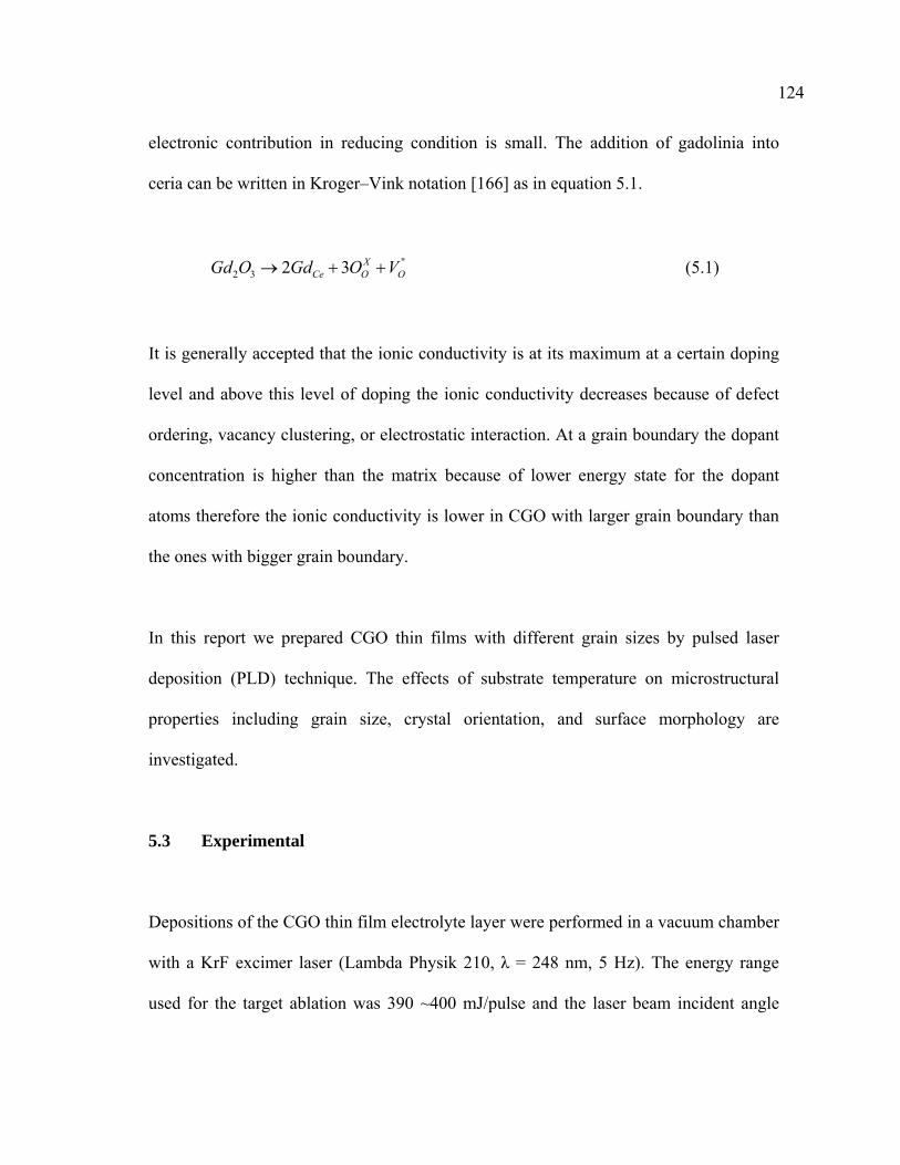
124
electronic contribution in reducing condition is small. The addition of gadolinia into
ceria can be written in Kroger–Vink notation [166] as in equation 5.1.
(5.1)
It is generally accepted that the ionic conductivity is at its maximum at a certain doping
level and above this level of doping the ionic conductivity decreases because of defect
ordering, vacancy clustering, or electrostatic interaction. At a grain boundary the dopant
concentration is higher than the matrix because of lower energy state for the dopant
atoms therefore the ionic conductivity is lower in CGO with larger grain boundary than
the ones with bigger grain boundary.
In this report we prepared CGO thin films with different grain sizes by pulsed laser
deposition (PLD) technique. The effects of substrate temperature on microstructural
properties including grain size, crystal orientation, and surface morphology are
investigated.
5.3 Experimental
Depositions of the CGO thin film electrolyte layer were performed in a vacuum chamber
with a KrF excimer laser (Lambda Physik 210, λ = 248 nm, 5 Hz). The energy range
used for the target ablation was 390 ~400 mJ/pulse and the laser beam incident angle
"2 3 2 3 X
Ce O OGd O Gd O V→ + +
125
was kept at 45˚. The focused laser beam energy density is approximately 10 J cm-2.
During deposition target was rotated and height of the target was adjusted for uniform
deposition rate through out the deposition process.
Yttria-stabilized zirconia (YSZ) single crystal substrate was selected for this experiment
because of its close lattice parameter match with CGO. The hot-pressed CGO target was
prepared by mixing the stoichiometric amounts of powders including CeO2, and Gd2O3.
All of the compounds were mixed and ground in a mortar and pestle with 1 wt% of poly-
ethylene glycol (PEG) as a binder for one hour and then ball milled for another two
hours. The ball milled powders were then uniaxially pressed into pellets of 33mm
diameter and 6mm in thickness at a pressure of 5tons/cm2 using hydraulic press. These
pellets were sintered at 1200 °C in a tube furnace for 10 hours in air at a ramping rate of
3˚C/min.
Thin film CGO electrolyte layers (about 1.5 µm–6.7 µm) were deposited through one-
step thin film deposition using pulsed laser deposition technique. The growth rate for
these thin films was controlled at about 1.7~7 nm/s at an oxygen partial pressure of
about 200 mTorr. The substrate temperature was varied from room temperature (RT) to
700 ºC to study the temperature effect on the microstructural change and the grain size
change of the of the thin film electrolyte layer. Microstructural characterization of these
thin films were performed by cross-section transmission electron microscopy (TEM)
using a JEOL2010 analytical electron microscope, a JEOL3000F analytical electron
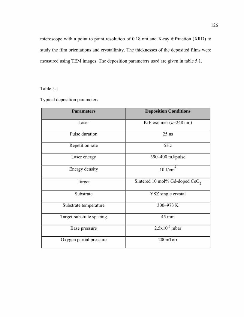
126
microscope with a point to point resolution of 0.18 nm and X-ray diffraction (XRD) to
study the film orientations and crystallinity. The thicknesses of the deposited films were
measured using TEM images. The deposition parameters used are given in table 5.1.
Table 5.1
Typical deposition parameters
Parameters Deposition Conditions
Laser KrF excimer (λ=248 nm)
Pulse duration 25 ns
Repetition rate 5Hz
Laser energy 390–400 mJ/pulse
Energy density 10 J/cm2
Target Sintered 10 mol% Gd-doped CeO2
Substrate YSZ single crystal
Substrate temperature 300–973 K
Target-substrate spacing 45 mm
Base pressure 2.5x10⁻⁶ mbar
Oxygen partial pressure 200mTorr
127
5.4 Results and Discussion
Thin films of CGO were prepared at different substrate temperatures. All the films were
deposited at 390~400 mJ/pulse laser energy, 200mTorr background O2 pressure, and
5Hz repetition rate for 15 minutes. Table 5.1 summarizes the detailed deposition
conditions. The typical thicknesses of the films deposited on YSZ substrates under the
above deposition conditions were about 1.5~6.7 µm. In PLD each laser pulse provides
target material with sufficient energy to grow only a sub monolayer of the desired phase.
The film growth mechanism depends on multiple factors such as target to substrate
distance, substrate temperature, laser ablation energy, and background oxygen pressure.
Among those process factors the substrate temperature is one of the most critical factors
in deciding film growth mechanism.
In this work, 10 mol% doping is chosen because at this doping level CGO shows the
highest lattice ionic conductivity around 500 ºC region even though the maximum grain
boundary conduction occurs at a composition of around 25% GdO1.95. We are focusing
on growing defect free epitaxial layer. It is known that the grain boundary region has a
lower ionic conductivity than the lattice and higher activation energy. Operating
temperature above 700 ºC these grain boundary effects become insignificant because of
high enough temperature to overcome high activation energy but in the intermediate
temperature regime, 400 ºC to 600 ºC it becomes significant. However, electrolyte
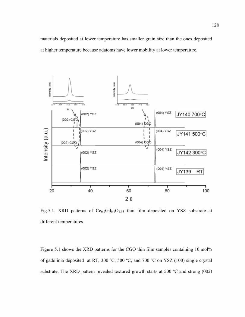
128
materials deposited at lower temperature has smaller grain size than the ones deposited
at higher temperature because adatoms have lower mobility at lower temperature.
Fig.5.1. XRD patterns of Ce0.9Gd0.1O1.95 thin film deposited on YSZ substrate at
different temperatures
Figure 5.1 shows the XRD patterns for the CGO thin film samples containing 10 mol%
of gadolinia deposited at RT, 300 ºC, 500 ºC, and 700 ºC on YSZ (100) single crystal
substrate. The XRD pattern revealed textured growth starts at 500 ºC and strong (002)
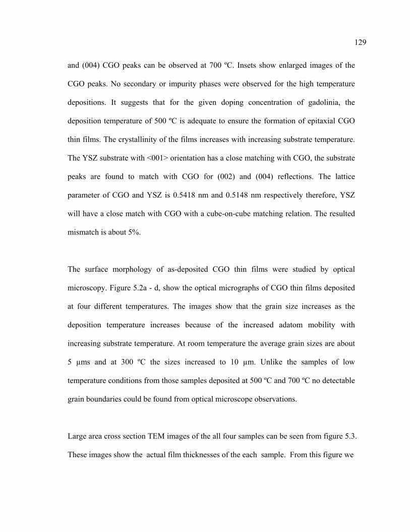
129
and (004) CGO peaks can be observed at 700 ºC. Insets show enlarged images of the
CGO peaks. No secondary or impurity phases were observed for the high temperature
depositions. It suggests that for the given doping concentration of gadolinia, the
deposition temperature of 500 ºC is adequate to ensure the formation of epitaxial CGO
thin films. The crystallinity of the films increases with increasing substrate temperature.
The YSZ substrate with <001> orientation has a close matching with CGO, the substrate
peaks are found to match with CGO for (002) and (004) reflections. The lattice
parameter of CGO and YSZ is 0.5418 nm and 0.5148 nm respectively therefore, YSZ
will have a close match with CGO with a cube-on-cube matching relation. The resulted
mismatch is about 5%.
The surface morphology of as-deposited CGO thin films were studied by optical
microscopy. Figure 5.2a - d, show the optical micrographs of CGO thin films deposited
at four different temperatures. The images show that the grain size increases as the
deposition temperature increases because of the increased adatom mobility with
increasing substrate temperature. At room temperature the average grain sizes are about
5 µms and at 300 ºC the sizes increased to 10 µm. Unlike the samples of low
temperature conditions from those samples deposited at 500 ºC and 700 ºC no detectable
grain boundaries could be found from optical microscope observations.
Large area cross section TEM images of the all four samples can be seen from figure 5.3.
These images show the actual film thicknesses of the each sample. From this figure we
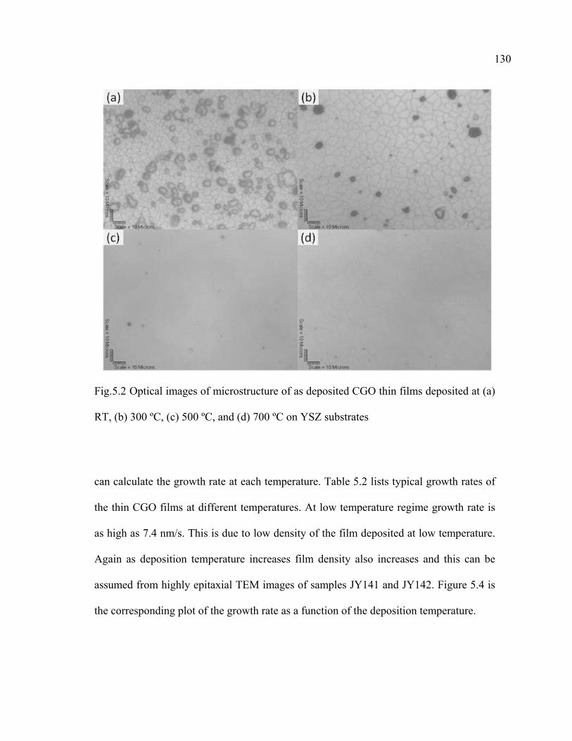
130
Fig.5.2 Optical images of microstructure of as deposited CGO thin films deposited at (a)
RT, (b) 300 ºC, (c) 500 ºC, and (d) 700 ºC on YSZ substrates
can calculate the growth rate at each temperature. Table 5.2 lists typical growth rates of
the thin CGO films at different temperatures. At low temperature regime growth rate is
as high as 7.4 nm/s. This is due to low density of the film deposited at low temperature.
Again as deposition temperature increases film density also increases and this can be
assumed from highly epitaxial TEM images of samples JY141 and JY142. Figure 5.4 is
the corresponding plot of the growth rate as a function of the deposition temperature.
131
Fig.5.3. Low magnification cross section TEM images of CGO thin films deposited at
(a) RT, (b) 300 ºC, (c) 500 ºC, and (d) 700 ºC
As the deposition temperature increases the growth rate decreases fast and above 500 °C
it shows very slow decrease because of increased crystallinity.
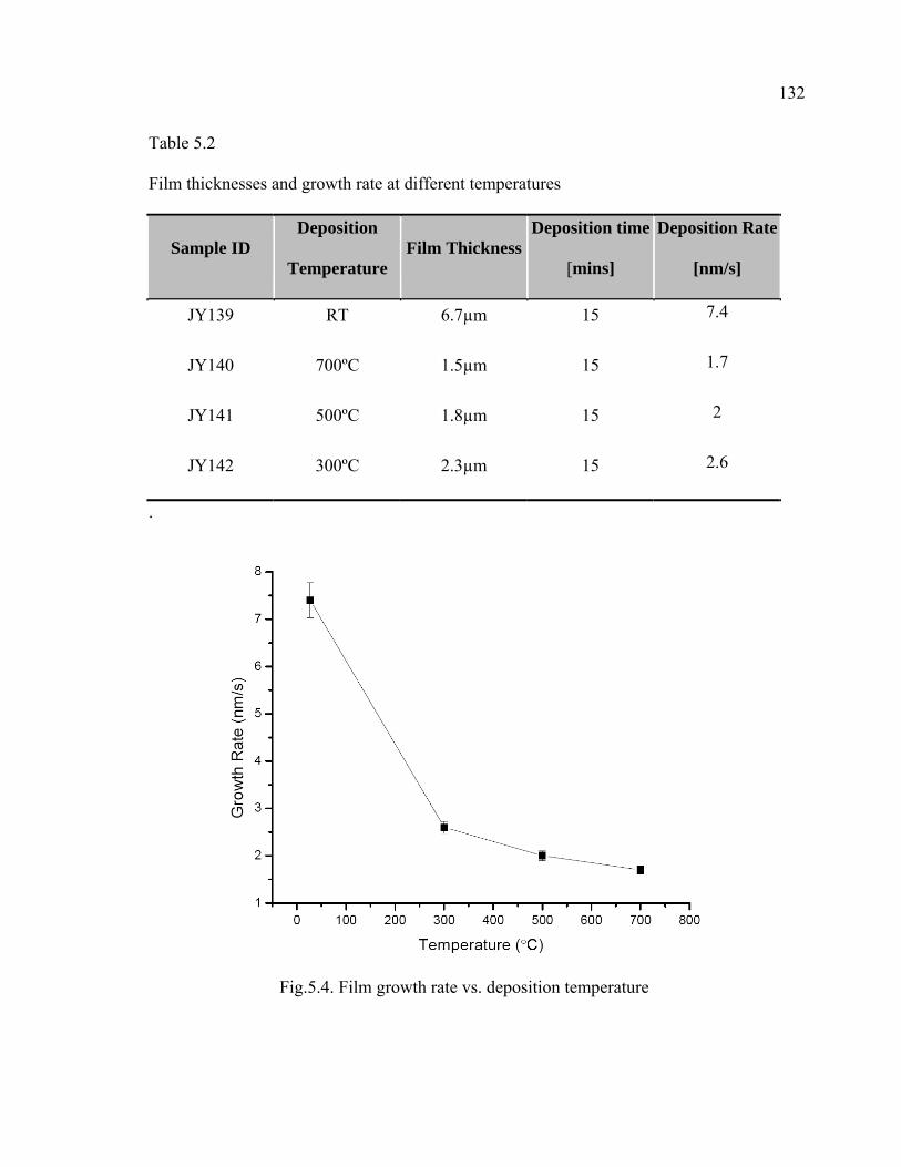
132
Table 5.2
Film thicknesses and growth rate at different temperatures
Sample ID Deposition
TemperatureFilm Thickness
Deposition time Deposition Rate
[mins] [nm/s]
JY139 RT 6.7µm 15 7.4
JY140 700ºC 1.5µm 15 1.7
JY141 500ºC 1.8µm 15 2
JY142 300ºC 2.3µm 15 2.6
.
Fig.5.4. Film growth rate vs. deposition temperature
133
Figure 5.5 shows the high magnification cross section TEM images of the films
deposited at all four temperatures. As can be verified from the Fig. 5.5a - d, at low
substrate temperature film grew as poly crystalline and the growth mechanism changes
to textured film growth at 300 ºC. From figure 4c and d, we can observe the highly
epitaxial films grown on YSZ substrates. It is interesting to note that the films are very
dense and free from cracks, and pores even from the sample deposited at RT. The X-ray
diffraction patterns enclosed in the figures also evidence the actual microstructures and
orientations of the films. The crystallinity of the films has been found to increase with
increasing substrate temperature.
5.5 Summary
We have successfully processed fully dense thin film CGO electrolyte with different
grain size. The crystallinity of the films has been found to increase with increasing
substrate temperature. CGO thin film deposited above 500 ºC starts to show epitaxial
growth on YSZ substrates. This dense CGO thin layer can increase gas tightness and
can decrease the interface charge transfer resistance by decreasing grain boundary size.
Hence lower total interface resistance between the electrolyte and cathode/anode layers.
The present study suggests that substrate temperature significantly influences the
microstructure of the films especially film grain size, and appropriate selections of the
process parameters are required to achieve CGO films with desired properties for high
efficiency SOFC applications.

134
Fig.5.5. High magnification crossection TEM images of CGO thin films deposited at (a)
RT, (b) 300 ºC, (c) 500 ºC, and (d) 700 ºC
135
CHAPTER VI
SUMMARY
The following list summarizes:
VANP: We have successfully processed nanostructured LSCO and LSCFO cathode thin
films for thin film SOFC. All the films grow as columnar grains, which leaves nanopores
in between the grains. The unique VANP structures in these cathode thin films penetrate
throughout the film thickness as deep as 2 μm and produce enhanced oxygen
conductance in the cathode layer. Additionally impedance measurements demonstrate
that the cathode thin films with VANPs have low polarization resistance values and
enhanced kinetic performance in the low temperature regime (400–700 °C).
VAN: We have successfully grown binary VAN interlayer of (LSCO)0.5 (CGO)0.5 in
between the cathode and electrolyte for high efficiency thin film SOFC. This unique
binary VAN structured interlayer effectively increases the cathode/electrolyte interface
area density (by 14~25 times depending on the interlayer thickness) and thus
significantly lowers the polarization resistance present at the cathode/electrolyte
interface. Hence a low cathode polarization resistance (9x10⁻⁴ Ω at 599oC, 2.39 Ω at
400oC) was achieved at low operation temperatures based on the impedance
measurements at low temperature regime (400~600 ºC). The interface area density can
be systematically controlled by varying the VAN interlayer thickness and column width,
which can be achieved through tuning the deposition parameters. As the VAN thickness
136
increases, the ASR shifts to lower values. By combining a CGO seed layer with the
VAN interlayer, we have demonstrated a record low ASR (4.84 x10⁻⁴ Ωcm2 at 599oC,
1.25 Ωcm2 at 400oC).
Electrolyte: We have successfully processed fully dense thin film CGO electrolyte with
different grain size. The crystallinity of the films has been found to increase with
increasing substrate temperature. CGO thin film deposited above 500 ºC starts to show
epitaxial growth on YSZ substrates. This dense CGO thin layer can increase gas
tightness and can decrease the interface charge transfer resistance by decreasing grain
boundary size. Hence lower total interface resistance between the electrolyte and
cathode/anode layers. The present study suggests that substrate temperature significantly
influences the microstructure of the films especially film grain size, and appropriate
selections of the process parameters are required to achieve CGO films with desired
properties for high efficiency SOFC applications.
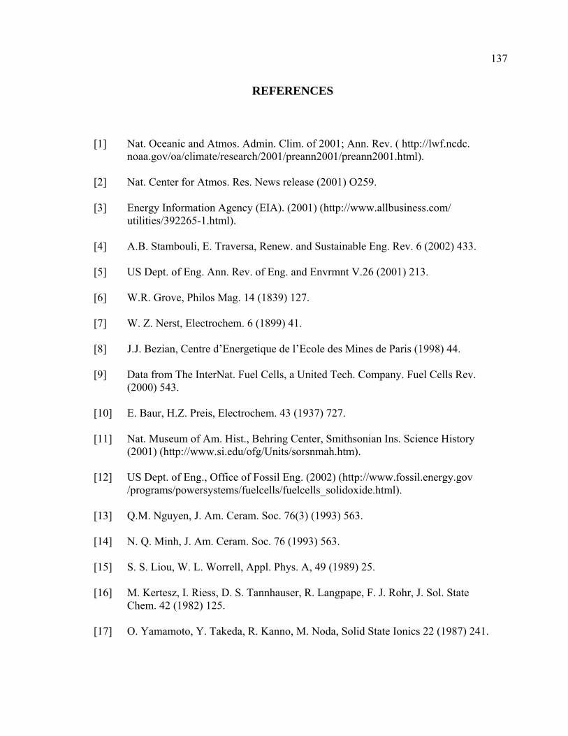
137
REFERENCES
[1] Nat. Oceanic and Atmos. Admin. Clim. of 2001; Ann. Rev. ( http://lwf.ncdc. noaa.gov/oa/climate/research/2001/preann2001/preann2001.html).
[2] Nat. Center for Atmos. Res. News release (2001) O259.
[3] Energy Information Agency (EIA). (2001) (http://www.allbusiness.com/ utilities/392265-1.html).
[4] A.B. Stambouli, E. Traversa, Renew. and Sustainable Eng. Rev. 6 (2002) 433.
[5] US Dept. of Eng. Ann. Rev. of Eng. and Envrmnt V.26 (2001) 213.
[6] W.R. Grove, Philos Mag. 14 (1839) 127.
[7] W. Z. Nerst, Electrochem. 6 (1899) 41.
[8] J.J. Bezian, Centre d’Energetique de l’Ecole des Mines de Paris (1998) 44.
[9] Data from The InterNat. Fuel Cells, a United Tech. Company. Fuel Cells Rev. (2000) 543.
[10] E. Baur, H.Z. Preis, Electrochem. 43 (1937) 727.
[11] Nat. Museum of Am. Hist., Behring Center, Smithsonian Ins. Science History (2001) (http://www.si.edu/ofg/Units/sorsnmah.htm).
[12] US Dept. of Eng., Office of Fossil Eng. (2002) (http://www.fossil.energy.gov /programs/powersystems/fuelcells/fuelcells_solidoxide.html).
[13] Q.M. Nguyen, J. Am. Ceram. Soc. 76(3) (1993) 563.
[14] N. Q. Minh, J. Am. Ceram. Soc. 76 (1993) 563.
[15] S. S. Liou, W. L. Worrell, Appl. Phys. A, 49 (1989) 25.
[16] M. Kertesz, I. Riess, D. S. Tannhauser, R. Langpape, F. J. Rohr, J. Sol. State Chem. 42 (1982) 125.
[17] O. Yamamoto, Y. Takeda, R. Kanno, M. Noda, Solid State Ionics 22 (1987) 241.
138
[18] Y. Ohno, S. Nagata, H. Sato, Solid State Ionics 3 (1981) 439.
[19] J. Mizusaki, Y. Mima, S. Yamauchi, K. Fueki, H. Tagawa, J. Solid State Chem. 80 (1989) 102.
[20] J. Mizusaki, J. Tabuchi, T. Matsuura, S. Yamauchi, K. Fueki, J. Electrochem. Soc. 136 (1989) 2082.
[21] Nextech Mater., Fuel Cell Mater. (2001) 256.
[22] E. S. Putna, J. Stubenrauch, J. M. Vohs, R. J. Gorte, Langmuir 11 (1995) 4832.
[23] J. T. S. Irvine, D. P. Fagg, J. Labrincha, F. M. B. Marques, Catal. Today 38 (1997) 467.
[24] E. P. Murray, T. Tsai, Nature 400 (1999) 649.
[25] S. Park, R. Craciun, V. Radu, R. J. Gorte, J. Electrochem. Soc. 146 (1999) 3603.
[26] B.C.H. Steele, A. Heinzel, Nature 414 (2001) 345.
[27] X. Chen, N.J. Wu, Z. H. Zhang, A. Ignatiev, Thin Solid Films 350(1-2) (1999) 1 30.
[28] C.C Sun, E.W. Hawk, E.F. Sverdrup, J. Electrochem. Soc. 119 (1972) 1433.
[29] G.F. Carini, H.U. Anderson, D.M. Aparlin, M.M. Nasrallah, Solid State Ionics 49 (1991) 233.
[30] R. Brawn, Rept. from the Solar Eng. Lab., Renewable and Sustainable Energy Reviews, 6 (2002) 433.
[31] A.J. Mc Evoy, Lab. de Photonique et des Interfaces. Ecole Polytechnique Fe´derale de Lausanne, Fuel cell tech. stat. and prosp. (1998) 154-158
(http://[email protected]/).
[32] Global Thermoelectric Inc. Ann. Rept. (2001) 32-37 (http://www.globalte.com /pdf/ar.pdf).
[33] Mater. Sci. and Res. Inc. 2000 Fuel Cell Seminar, Portland, OR. (2000) 212.
[34] California Energy Commission. (2001) 286 (http://www.accessmylibrary.com/ coms2/summary_0286-10717979_ITM).

139
[35] S. A. Boudghene, E. Traversa, Proc. of the Premier Seminaire (2001) 631.
[36] D. B. Chrisey, G. K. Hubler, Pulsed Laser Deposition, Wiley-InterSci., New York (1994) 5.
[37] R. K. Singh, D. H. Lowndes, D. B. Chrisey, E. Fogarassy, J. Narayan, Mater. Res. Soc. 526 (1998) 47.
[38] J. E. Mahan, Wiley-InterSci., New York (2000) 133-151.
[39] R. K. Singh, J. Narayan, A. K. Singh, J. Krishnawmy, Appl. Phys. Lett. 54 (1989) 2271.
[40] R. K. Singh, O. W. Holland, J. Narayan, J. Appl. Phys. 68 (1) (1990) 233.
[41] R. K. Singh, J. Narayan, Phys. Rev. B. 41 (13) (1990) 8843.
[42] B. D. Cullity, Elements of X-Ray Diffr., Addison-Wesley, Inc. MA (1982).
[43] L. Azaroff, R. Kaplow, N. Kato, R. Weiss, A. Wilson, R. Young, X-ray Diffr., McGraw-Hill, Inc. New York (1974).
[44] D. B. Williams, Pract. Anal. Elec. Microsc. in Mater. Sci., Philips Elec. Ic. Instrum., Inc. Elec. Opt. Publishing Group, New York (1984).
[45] D. B. Williams, and C. B. Carter, Trans. Elec. Microsc., Plenum Press, New York (1996).
[46] J. Spence, Exp.al High Resolut. Elec. Microsc., Oxford Univ. Press, New York (1988).
[47] J. W. Eddington, Pract. Elec. Microsc. in Mater. Sci., V.11 (1976) 133.
[48] S.J. Pennycook, D.E. Jesson, UltraMicrosc. 37 (1991) 14.
[49] D.B. Williams, C.B. Carter, Trans. Elec. Microsc., Plenum Press, New York (1996) 22.
[50] C.E. Hall, Intro. to Elec. Microsc., McGraw Hill, New York (1953) 229.
[51] L.M. Brown, J. Yuan, N.D. Browning, S.J. Pennycook, Char. of High Tc (Tc:
Critical Temperature) Mater. and Dev. by Elec. Microsc., Cambridge Univ. Press, Cambridge (2000) 40
140
[52] D.B. Williams, C.B. Carter, Trans. Elec. Microsc., Plenum Press, New York (1996) 147.
[53] D.B. Williams, C.B. Carter, C. B, Trans. Elec. Microsc., Plenum Press, New York (1996) 79.
[54] R. W. Carpenter, Elec. Microsc. in Mater. Sci, (Ed. P. G. Merli) 315 (1991) 81.
[55] N.D. Browning, S.J. Pennycook, J. Microsc. 180 (1995) 230.
[56] M. Haider, J. Zach, Elec. Microsc. 1 (1998) 53.
[57] O. L. Krivanek, N. Dellby, A. J. Spence, L. M. Brown, Elec. Microsc. 1 (1998) 55.
[58] A. R. Lupini, O. L. Krivanek, Elec. Microsc. 1 (1998) 59.
[59] D.B. Williams, C.B. Carter, Trans. Elec. Microsc., Plenum Press, New York (1996) 359.
[60] H. Yokokawa, N. Sakai, T. Horita, K. Yamaji, M.E. Brito, H. Kishimoto, J. Alloys Compd. 433 (2007) 193.
[61] B. Butz, P. Kruse, H. St¨ormer, D. Gerthsen, A. M¨uller, A. Weber, E. Ivers- Tiff´ee, Solid State Ionics 177 (2006) 3275.
[62] D. Larrain, J. V. Herle, D. Favrat, J. Power Sources 161 (2006) 392.
[63] J.R. Macdonald, Impedance Spectrosc.—Emphasizing Solid Mater. and Sys., John Wiley & Sons, New York (1987).
[64] J.R. Macdonald, Impedance Spectrosc.—Theory Exp. and Appl., John Wiley & Sons, New York (2005).
[65] Z. Stoynov, D. Vladikova, Differ. Impedance Anal., Marin Drinov Acad. Publishing House, Sofia (2005).
[66] Z. Stoynov, B. Grafov, B. S. Stoynova, V. Elkin, Electrochem. Impedance, Publishing House “Nauka”, Moscow (1991).
[67] A. Lasia, in: B.E. Conway, J. Bockris, R. White (Eds.), Electrochem. Impedance Spectrosc. and its Appl.-Modern Aspects of Electrochem., Kluwer Acad., Plenum Publishers, New York, vol. 32 (1999).
141
[68] C. Gabrielli, Ident. of Electrochem. Processes by Freq. Response Anal. Tech. Rept. 004/83 (1998).
[69] C. Gabrielli, Use and Appl. of Electrochem. Impedance Tech., Tech. Rept. 24 (1997).
[70] A. Barbucci, P. Carpanese, G. Gerisola, M. Viviani, Solid State Ionics 176 (2005) 1753.
[71] K. Huang, J. Electrochem. Soc. 151 (5) (2004) A716.
[72] K. Huang, J. Electrochem. Soc. 151 (5) (2004) H117.
[73] J.W. Kim, A.V. Virkar, K.Z. Fung, K. Mehta, S.C. Singhal, J. Electrochem. Soc. 146 (1) (1999) 69.
[74] A.V. Virkar, J. Chen, C.W. Tanner, J.W. Kim, Solid State Ionics 131 (1–2) (2000) 189.
[75] S.H. Chan, K.A. Khor, Z.T. Xia, J. Power Sources 93 (2001) 130.
[76] S.H. Chan, Z.T. Xia, J. Appl. Electrochem. 32 (2002) 339.
[77] J. Bard, L.R. Faulkner, Electrochem. Methods—Fundam. and Appls., John Wiley & Sons, New York (2001).
[78] J.W. White, Proc. IEEE 59 (1971) 98.
[79] J.W. White, Proc. of the 6th Ann. Princeton Conf. on Inf. Sci. and Sys. (1972) 173.
[80] R. de, L. Kronig, J. Opt. Soc. Am. 12 (1926) 547.
[81] H.A. Kramers, Z. Phys. 30 (1929) 521.
[82] H.W. Bode, Network Anal. and Feedback Amp. Des. (1945) Chapter 14.
[83] Z. Stoynov, Electrochim. Acta 38 (1993) 1919.
[84] K. Darowicki, J. Electroanal. Chem. 486 (2000) 101.
[85] K. Darowicki, J. Orlikowski, G. Lentka, J. Electroanal. Chem. 486 (2000) 106.
142
[86] S. Rosvall, M. Honeychurch, D. Elton, A. Bond, J. Electroanal. Chem. 515 (2001) 8.
[87] K. Darowicki, P. ´ Slepski, Electrochim. Acta 49 (2004) 763.
[88] K. Darowicki, Corros. Sci. 37 (1995) 913.
[89] J.R. Wilson, D.T. Schwartz, S.B. Adler, Electrochim. Acta 51 (2006) 1389.
[90] J.R. Macdonald, D.R. Franceschetti, J. Chem. Phys. 68 (1978) 1614.
[91] M. Nagata, Y. Itoh, H. Iwahara, Solid State Ionics 67 (1994) 215.
[92] S.B. Adler, J. Electrochem. Soc. 149 (2002) E166.
[93] G. Hsieh, S.J. Ford, T.O. Mason, L.R. Pederson, Solid State Ionics 91(1996) 191.
[94] G. Hsieh, T.O. Mason, L.R. Pederson, Solid State Ionics 91 (1996) 203.
[95] G. Hsieh, T.O. Mason, E.J. Garboczi, L.R. Pederson, Solid State Ionics 96 (1997) 153.
[96] G. Hsieh, S.J. Ford, T.O. Mason, L.R. Pederson, Solid State Ionics 100 (1997) 297.
[97] F.P.F.V. Berkel, F.H.V. Heuneln, J.P.P. Huijamans, Solid State Ionics 72 (1994) 240.
[98] G.W. Walter, J. Electroanal. Chem. 118 (1981) 259.
[99] G.W. Walter, Corros. Sci. 26 (1986) 681.
[100] Gamry Instrum., Electrochem. Impedance Spectrosc. Theory: A Primer, (http://www.gamry.com/App Notes/EIS Primer/EIS Primer.htm), (1997–2005).
[101] J.D. Kim, G.D. Kim, J.W. Moon, Y. Park, W.H. Lee, K. Kobayashi, M. Nagai, C.E. Kim, Solid State Ionics 143 (2001) 379.
[102] S.Z. Wang, Y. Jiang, Y.H. Zhang, J.W. Yan, W.Z. Li, Solid State Ionics 115 (1998) 291.
[103] E.P. Murray, T. Tsai, S.A. Barnett, Solid State Ionics 110 (1998) 235.
[104] J.P. Diard, B. Le Gorrec, C. Montella, J. Electroanal. Chem. 205 (1986) 77.
143
[105] J.P. Diard, P. Landaud, B. Le Gorrec, C. Montella, J. Electroanal. Chem. 352 (1993) 1.
[106] J.P. Diard, B. Le Gorrec, C. Montella, J. Electroanal. Chem. 326 (1992) 13.
[107] J.P. Diard, B. Le Gorrec, C. Montella, C. Montero-Ocampo, J. Electroanal. Chem. 352 (1993) 1.
[108] J.I. Gazzarri, O. Kesler, J. Power Sources 167 (2007) 100.
[109] J.I. Gazzarri, O. Kesler, J. Power Sources 167 (2007) 430.
[110] A. Barbucci, R. Bozzo, G. Gerisola, P. Costamagna, Electrochem. Acta 47 (2002) 2183.
[111] A. Barbucci, M. Viviani, P. Carpanese, D. Vladikova, Z. Stoynov, Electrochim. Acta 51 (2006) 1641.
[112] T. Kato, K. Nozaki, A. Negishi, K. Kato, A. Momma, Y. Kaga, S. Nagata, K. Takano, T. Inagaki, H. Yoshida, K. Hosoi, K. Hoshino, T. Akbay, J. Akikusa, J. Power Sources 133 (2004) 169.
[113] A. Liliya, Y.X. Dunyushkina, S.B. Lu, Adlera, J. Electrochem. Soc. 152 (2005) A1668.
[114] H. Kuboyama, T. Shoho, M. Matsunaga, Electrochem. Proc. 97 (1997) 404.
[115] T. Kato, K. Nozaki, A. Negishi, K. Kato, A. Momma, Y. Kaga, S. Nagata, K. Takano, T. Inagaki, H. Yoshida, et al., J. Power Sources 133 (2004) 169.
[116] S.J. Skinner, Int. J. Inorg. Mater. 3 (2001) 113.
[117] B.C.H. Steele, J. Mater. Sci. 36 (2001) 1053.
[118] J.M. Ralph, A.C. Schoeler, M. Krumpelt, J. Mater. Sci. 36 (2001) 1161.
[119] Y. Teraoka, T. Nobunaga, N. Yamazoe, Chem. Lett. (1988) 503.
[120] Y. Teraoka, H.M. Zhang, K. Okamoto, N. Yamazoe, Mater. Res. Bull. 23 (1988) 51.
[121] Y. Matsumoto, S. Yamada, T. Nishida, E. Sato, J. Electrochem. Soc. 127 (1999) 2360.
144
[122] A. Petric, P. Huang, F. Tietz, Solid State Ion. 135 (2000) 719.
[123] J. Fleig, J. Power Sources 105 (2002) 228.
[124] P.B. Barna, M. Adamik, Thin Solid Films 317 (1998) 27.
[125] I. Petrov, P.B. Barna, L. Hultman, J.E. Greene, J. Vac. Sci. Technol. A21 (5) (2003) 5117.
[126] S. Mahieu, et al. Thin Solid Films 515 (4) (2006) 1229.
[127] B.A. Movchan, A.V. Demchishin, Phys. Met. Mettalogr. 28 (1969) 83.
[128] J.A. Thornton, J. Vac. Sci. Technol. 11 (4) (1974) 666.
[129] V. Dusastre, J.A. Kilner, Solid State Ion. 126 (1999) 163.
[130] E.P. Murray, M.J. Sever, S.A. Barnett, Solid State Ion. 148 (2002) 148.
[131] L. Baque, A. Serquis, N.Grunbaum, F. Prado, A. Caneiro, Mat. Ges. Soc. Symp, Proc. 928 (2006), 16.
[132] N. Grunbaum, et al. Solid state Ion. 177 (2006) 907.
[133] M. Kleitz, T. Kloidt, L. Dessemond, (1993) 89.
[134] S.B. Adler, Chem. Rev. 104 (2004) 479.
[135] H. Apfel, et al. J. Power Sources 154 (2) (2006) 370.
[136] B. Kenney, K. Karan, Solid State Ionics 178 (3-4) (2007) 297.
[137] M.H. Hung, M.V.M. Rao, D.S. Tsai, Mater. Chem. Phys. 101 (2-3) (2007) 297.
[138] J. Deseure, et al. J. Appl. Electrochem. 37 (1) (2007) 129.
[139] M. Sase, et al. Solid State Ionics 177 (19-25) (2006) 1961.
[140] E. Koep, et al. J. Power Sources 161 (1) (2006) 250.
[141] S.P. Yoon, et al. J. Power Sources 136 (1) (2004) 30.
[142] J. Yoon, et al. Appl. Surf. Sci. 254 (1) (2007) 266.
145
[143] B.S. Kang, et al. Appl. Phys. Lett. 88 (19) (2006).
[144] J.L. MaCmanus-Driscoll, et al. Nat. Mater. 7 (4) (2008) 314.
[145] Z. Bi, J. Lee and H. Wang, in preparation for Appl. Phys. Lett. (2008)
[146] A.O. Stoermer, J.L.M. Rupp, L.J. Gauckler, Solid State Ionics 177 (19-25) (2006) 2075.
[147] B.C.H. Steele, Solid State Ionics 129 (1-4) (2000) 95.
[148] C.R. Doshi, V.I. Richards, J.D. Cartex, X.P. Way, M. Krumpett, J Electrochem. Soc. 146(4) (1999) 1273.
[149] B.C.H. Steel, Solid State Ion 129(1–4) (2000) 95.
[150] S. de Souza, S.J. Visco, L.C. de Jonghe, Solid State Ionics 98 (1997) 57.
[151] J.W. Kim, A.V. Virkar, K.Z. Fung, K. Mehta, S.C. Singhal, J. Electrochem. Soc. 146 (1999) 69.
[152] J. Will, A. Mitterdorfer, C. Kleinlongel, D. Perednis, L.J. Gauckler, Solid State Ionics 131 (2000) 79.
[153] R. Maric, S. Ohara, T. Fukui, H. Yoshida, M. Nishimura, T. Inagaki, K. Miura, J. Electrochem. Soc. 146 (1999) 2006.
[154] T. Ishihara, T. Shibayama, M. Honda, H. Nishiguchi, Y. Takita, J. Electrochem. Soc. 147 (2000) 1332.
[155] K. Wang, J.H. Wan, J.B. Goodenough, J. Electrochem. Soc. 148 (2001) A788.
[156] J.W. Yan, Z.G. Lu, Y. Jiang, Y.L. Dong, C.Y. Yu, W.Z. Li, J. Electrochem. Soc.149 (2002) A1132.
[157] R. Doshi, V.L. Richards, J.D. Carter, X. Wang, M. Krumpelt, J. Electrochem. Soc. 146 (1999) 1273.
[158] C. Xia, F. Chen, M. Liu, Electrochem. Solid-State Lett. 4 (2001) A52.
[159] S.P. Jiang, Y.J. Leng, S.H. Chan, K.A. Khor, Electrochem. Solid-State Lett. 6 (2003) A67.
[160] E.P. Murray, M.J. Sever, S.A. Barnett, Solid State Ionics 148 (2002) 27.

146
[161] V. Dusastre, J.A. Kilner, Solid State Ionics 126 (1999) 163.
[162] C. Xia, M. Liu, Adv. Mater. 14 (2002) 521.
[163] T. Ishihara, K. Sato, Y. Takita, J. Am. Ceram. Soc. 79 (1996) 913.
[164] J.A. Kilner, Solid State Ion 129 (2000) 13.
[165] J.A. Kilner, R.J. Brook, Solid State Ionics 6(3) (1982) 237.
[166] F. Kroger, H.J. Vink, F. Seitz, D. Turnbull(eds), Solid State Phys., Academic Press, New York (1965).

147
VITA
Name: Jongsik Yoon
Address: Department of Electrical and Computer Engineering,
Texas A&M University,
706 Jack E. Brown Engineering Bld.,
College Station, TX 77843
Email Address: [email protected]
Education: B.S., Chemistry, Yonsei University, Korea 1999
M.S., Electrical Engineering, University of Southern California,
2004
Ph.D., Electrical and Computer Engineering, Texas A&M
University, 2008
This dissertation was typed by the author.