nanomechanical systems from 2d...
TRANSCRIPT

Nanomechanical Systems from 2D Materials
by
Xinghui Liu
B.S., Shaanxi University of Science and Technology, 2005
M.S., Shaanxi University of Science and Technology, 2008
A thesis submitted to the
Faculty of the Graduate School of the
University of Colorado in partial fulfillment
of the requirement for the degree of
Doctor of Philosophy
Department of Mechanical Engineering
2014
This thesis entitled:
Nanomechanical Systems from 2D Materials
written by Xinghui Liu
has been approved for the Department of Mechanical Engineering
J. Scott Bunch
Committee Chairman, Department of Mechanical Engineering
Xiaobo Yin
Department of Mechanical Engineering
Date
The final copy of this thesis has been examined by the signatories, and we
Find that both the content and the form meet acceptable presentation standards
Of scholarly work in the above mentioned discipline.

iii
Liu, Xinghui (Ph.D., Department of Mechanical Engineering)
Nanomechanical Systems from 2D Materials
Thesis directed by Professor J. Scott Bunch
ABSTRACT
The isolation of graphene, a single atomic layer of carbon atoms, leads to the exploration
of a group of new materials - 2 dimensional (2D) crystals, which have unique properties in
mechanical, electrical and optical fields. This thesis demonstrates our work on the development
of nanomechanical systems from 2D materials (graphene and MoS2) and using them for the
study of material properties.
At first, we developed large arrays of 3-terminal graphene NEMS switches with a novel
design, which help the devices to achieve low actuation voltages (down to ~3V), improved
reliability and mechanical integrity. These switches may find applications in mechanical
computing, data storage, and RF communication, and the design can be used for other 2D
materials based NEMS switches. We also studied the electromechanical properties of the devices.
A study of the threshold switching voltages is carried out, and the switching voltage is simulated
with a finite element model which includes nonlinear mechanics. From this we deduce a scaling
relation between the switching voltage and device dimensions.

iv
Next, we present a unique nanomechanical configuration that allows us to determine the
interfacial forces between graphene and Au/SiO2. The nature of the interfacial forces at ~ 10 - 20
nm separations is consistent with an inverse fourth power distance dependence, implying that the
interfacial forces are dominated by van der Waals interactions. Furthermore, the strength of the
interactions is found to increase linearly with the number of graphene layers. The experimental
approach can be used to measure the strength of the interfacial forces for other atomically thin
two-dimensional materials, and help guide the development of nanomechanical devices such as
switches, resonators, and sensors.
Finally, we show the modulation of electronic band structure in monolayer suspended
MoS2 membranes with local biaxial strain at the center of a spherical blister. We observed a
linear direct band gap (A peak) decrease rate of ~100 meV/% strain in monolayer MoS2. Future
work includes biaxial strain engineering on bilayer and trilayer MoS2.

v
Acknowledgement
Working on my Ph.D. thesis during the last 6 years in Boulder is an unforgettable life
journey for me. I think Boulder is a perfect place for living, but what I enjoy most was the
research during this period of time. So at first I want to thank my advisor, Professor Scott Bunch,
for bringing me into an exciting area of scientific study and leading me to the successful
completion of this thesis. After trying to make nano size metal powders for about 2 years in
China, I realized that there is a lot of room and fun as well after scaling the size of materials into
the nano scale. When I was looking for the smallest material I can work on in the department
after arriving at CU, Dr. Bunch introduced me to graphene, which is amazingly one atom thick.
With this unique structural property, there are tons of potentials to explore and the primary one
of them is to make transistors from graphene. Other than traditional field effect transistors
(FETs), he led me to explore some unusual transistors from graphene, and the work in the Ch. 5
is one of them that finally interested us most. Within all those years of making transistors, his
passion and wisdom always inspired me. Furthermore, Dr. Bunch taught me how to keep patient
when facing failures and how to tackle difficult problems with creativity. All this training
significantly accelerated my speed to complete the work in Ch. 6 and Ch. 7.
It turns out that I am the first and last group member in Dr. Bunch’s lab in CU, and I want
to say it was lots of fun to work with all the group members during this period of time. Steven
Koenig and Phi Pham were the first batch of students in the lab and contributed a lot for building
the lab. Luda Wang came one year later and was always happy to help with different projects.
Lauren Cantley started working with me in 2010 summer REU program followed by Miguel
Rodriguez and Mariah Szpunar in 2011. Here I want to thank them all for their significant

vi
contribution to this thesis. I also enjoy hanging out with the group members after working in the
lab.
The completion of this thesis is based on the collaboration of a lot of other groups, and I
want to give my special thanks to all the collaborators. Without high quality CVD graphene
grown and dry transferred by Ji Won Suk and his colleagues from Professor Rodney Ruoff’s
group, we would need much more work to develop large arrays of 3-terminal graphene NEMS
switches shown in Ch. 5. The analysis of experimental results shown in Ch. 5 and Ch. 6
developed by Narasimha Boddeti from Professor Martin Dunn’s group helped us have a better
understanding of what is going on and improve the quality of the papers significantly. The
insights directly from Professor Martin Dunn, Professor Victor Bright, Professor Charles Rogers,
Professor Jianliang Xiao, and Professor Xiaobo Yin in different issues of this thesis are very
helpful. I also want to thank them for serving as my committee members together with Professor
Thomas Schibli and thank them all for reading this thesis.
To fabricate the graphene/MoS2 based nanomechanical devices and to probe the
properties of the 2D materials requires a variety of facilities. The facilities available in CNL
make all the microfabrication possible, and Jan Vanzeghbroeck together with other staff in the
lab were very helpful with the training of the equipment and solving problems encountered in
fabrication. Besides, I want to thank Professor Victor Bright and Professor Charles Rogers for
allowing me to use the probe stations in their labs, and Professor Rishi Raj and Professor Conrad
Stoldt for the Raman microscopes, and Professor YC Lee for different kinds of facilities in his
lab.
I want to thank my family who I owe so much being in a foreign country and to whom I
dedicate this thesis. I want to thank my mom, who brought up my elder sister and me alone since

vii
I was 10, and it is all her love and support through all these years that encourage me to always
keep improving myself and to come to US working on a Ph.D. My sister, two years older than
me, is a good friend and mentor as well, and she always supports my decisions and keeps me as a
priority. I would like to thank my friends as well. We share many wonderful memories exploring
different cities and national parks across the US and trying different kinds of food around.
Inevitably, I might leave someone deserving my appreciation in helping me complete this
thesis. Therefore, I am thankful to all of those who have contributed in some way to my success.

viii
Contents
Chapter 1 Introduction .................................................................................................................... 1
1.1 Introduction…………………………………………………………………. ................. 1
1.2 Outline……………………………………………………………………….. ................ 2
1.3 Nanomechanical Systems……………………………………………………….. ........... 3
1.4 Top-down versus Bottom-up Fabrication……………………………………… ............ 5
1.5 Conclusion………………………………………………………………………. ........... 7
Chapter 2 Graphene, MoS2 and Beyond ......................................................................................... 8
2.1 2D materials……………………………………………………………………. ............ 8
2.2 Graphene…………………………………………………………………………… .... 11
2.3 MoS2……………………………………………………………………………… ....... 15
2.4 Conclusion………………………………………………………………………… ...... 18
Chapter 3 Nanomechanics of 2D Materials .................................................................................. 19
3.1 Mechanical Properties of Membranes………………………………………. ............... 19
3.2 Bulge Test……………………………………………………………………….. ........ 21
3.3 Contact Adhesion………………………………………………………………………24
3.4 Blister Test…………………………………………………………………….. ........... 24
3.5 Van der Waals Force…………………………………………………………. ............. 25
3.6 Electromechanical Actuation……………………………………………………. ........ 26
3.7 Pull in Phenomenon…………………………………………………………… ........... 27
3.8 Conclusion……………………………………………………………………… .......... 27
Chapter 4 Nanomechanical Systems: Review of NEMS Switches, Interfacial Forces and Strain
Engineering ................................................................................................................................... 28
4.1 Nanoelectromechanical switches……………………………………………… ........... 28
4.1.1 Graphene Based NEMS Switches ........................................................................... 29
4.1.2 Carbon Nanotubes Based NEMS switches ............................................................. 35
4.1.3 Thin film lateral NEMS Switches ........................................................................... 37
4.1.4 NEMS memories ..................................................................................................... 40
4.2 Theories and Measurements of van der Waals Forces in Nanomechanical Systems..... 41

ix
4.2.1 Theories on van der Waals Forces .......................................................................... 42
4.2.2 Early Measurements of van der Waals Force ......................................................... 44
4.2.3 Measurements of van der Waals Force in Micro/Nanomechanical Systems .......... 47
4.3 Strain Engineering………………………………………………………………. ......... 55
4.3.1 Strain Engineering in Graphene .............................................................................. 55
4.3.2 Electronic Band Structure in MoS2 ......................................................................... 56
4.3.3 Strain Engineering in MoS2 .................................................................................... 57
4.4 Conclusion……………………………………………………………………. ............. 58
Chapter 5 Large Arrays and Properties of 3-Terminal Graphene Nanoelectromechanical Switches
....................................................................................................................................................... 59
5.1 Introduction………………………………………………………………….. .............. 59
5.2 Device Design…………………………………………………………………… ........ 60
5.3 Device Fabrication………………………………………………………………. ........ 62
5.4 Electrical Measurement……………………………………………………….. ............ 66
5.5 Verification of Electromechanical Switching……………………………………. ....... 68
5.6 Temperature Dependence…………………………………………………….. ............. 70
5.7 Statistics of Threshold Voltage………………………………………………… .......... 72
5.8 Modeling and Analysis……………………………………………………………....... 72
5.9 Size Scaling…………………………………………………………………… ............ 77
5.10 Sliding during Switching……………………………………………………… ............ 79
5.11 Graphene 3-Terminal Switches with a Different Geometry…………………….. ........ 79
5.12 Conclusion………………………………………………………………………. ......... 81
Chapter 6 Measurement of Interfacial Forces in Graphene Membranes ...................................... 82
6.1 Introduction……………………………………………………………………… ........ 82
6.2 Fabrication…………………………………………………………………….. ............ 83
6.3 Observation of Pull-in Instability…………………………………………….. ............. 83
6.4 Analytical Model………………………………………………………………… ........ 86
6.5 Finite Element Analysis………………………………………………………. ............ 87
6.6 Layer Dependence…………………………………………………………….. ............ 91
6.7 Power Law Study………………………………………………………………… ....... 93
6.8 Materials Dependence………………………………………………………….. .......... 95

x
6.9 Deformation of Graphene Membranes by vdW Force………………………… ........... 97
6.10 Conclusion……………………………………………………………………….. ........ 99
Chapter 7 Biaxial Strain Engineering in Suspended Monolayer MoS2 ..................................... 100
7.1 Introduction……………………………………………………………………… ...... 100
7.2 Fabrication………………………………………………………………………. ....... 101
7.3 Biaxial Straining……………………………………………………………….. ......... 103
7.4 Direct Bandgap Energy Tuning in Monolayer……………………………………… . 103
7.5 Conclusion…………………………………………………………………………. ... 105
Appendix ..................................................................................................................................... 106
A1. Counting the number of graphene layers…………………………………………… ..... 106
A2. Analytical Model for Pull-in Instability in Graphene Membrane………………………. 110
A3. Calculation of Constants for Interfacial Forces……………………………………. ....... 114
Reference .................................................................................................................................... 117
xi
List of Figure
Figure 1.1 Nanomechanical Systems: a) NEMS resonator from exfoliated graphene,[7]
b)
nanomechanical mass sensor to detect molecules (adapted from http://the-briefing.com)............ 4
Figure 2.1 Common 2D materials: graphene, MoS2, hBN, WSe2, and Fluorographene.[24]
……. 10
Figure 2.2 Electrical and mechanical properties in graphene a) Ambipolar electric field effect in
single-layer graphene.[22]
b) (lower) SEM images of the suspended CVD graphene film over
holes. (upper) Schematic of the device. c) Force-displacement curve of the SG graphene film in
AFM nanoindentation. insets are AFM images of graphene film before and after nanoindentation.
Scale bar is 3 μm and 1 μm for (b) and (c), respectively.[28]
d) AFM images of gas impermeable
graphene membranes when bulged down (upper) and bulged down (lower)…………………... 12
Figure 2.3 CVD growth and transfer of graphene a) SEM image of low-density graphene
domains on OR-Cu exposed to O2. b) Optical image of centimeter-scale graphene domains
on…………………………………………………………………………………………………14
Figure 2.4 a) Atomic structure of monolayer MoS2.[10]
b) Optical image of exfoliated monolayer
MoS2 flake. c) Optical image of CVD MoS2 flake. d) Simplified band structure of bulk
MoS2.[43]
………………………………………………………………………………………… 16
Figure 2.5 a) Schematic of MoS2 top gate field effect transistor. b) Ids vs Vg.[45]
c) Schematic of
MoS2 photodetector. d) Photoresistivity over illumination wavelength. [46]
…………………… 16
Figure 4.1 Graphene NEMS switches a) Schematic diagram of an all CVD graphene switch
from a cross sectional view and a top view. b) SEM images of suspended graphene and tear on
graphene.[71]
c) Schematic of the 3-terminal graphene switches with a STM probe. d) SEM image
of the device.[73]
……………………………………………………………………………….... 30
Figure 4.2 a) SEM image showing the breakdown of graphene. b) Electrical measurement
showing the breakdown of graphene. c) Electrical measurement of graphene atomic switch. d)
Schematic showing the atomic switching of the device.[74]
e) The SEM images of ON and OFF
state for the atomic switch with suspended graphene. The scale bar is 1 μm.[75]
………………. 32
Figure 4.3 a) (A through E) Dark-Field optical micrographs of the nanotube arms at potentials of
0, 5, 7.5, 8.3, and 8.5 V, respectively. Scale bars, 1 mm. b) Dark-field optical micrographs
showing the sequential process of nanotweezer manipulation of polystyrene nanoclusters
containing fluorescent dye molecules.[76]
c) A schematic illustration of the CNT-based
electromechanical switch device. d) SEM image of the device: The length and diameter of the
MWCNTs are about 2 μm and 70 nm, respectively. e) Current-voltage characteristics of

xii
switching action in an ambient environment; the electromechanical movement of MWCNTs
provides the on and off states. The scale bar corresponds to 1 μm. [77,78]
……………………… 34
Figure 4.4 a) Schematic diagram of the carbon nanotube relay, b) IV characteristics of a
nanotube relay initially suspended approximately 80 nm above the gate and drain electrodes. Vsd
= 0.5 V.[79]
c) Schematic of the device. d) SEM image of the device. e) IV characteristic of the
device. f) Response time measurement showing the response time equals 2.8 ns.[80]
………….. 36
Figure 4.5 a) Layout design of the lateral switch, b) SEM image of the device, c) IV
characteristic of the device.[83]
d) & e) SEM image of SiC NEMS inverter.[11]
………………... 38
Figure 4.6 a) Schematic drawing on the main parts of the apparatus for van der Waals force
measurement. In jump experiments a double cantilever spring was used. In resonance
experiments a single cantilever “bimorph” spring was used. b) 3D rendering of the half mica
cylinders. c) Variation of the power law of the van der Waals force between crossed mica
cylinders with distance D. The curve is based on the combined results of a number of jump and
resonance experiments.[88]
……………………………………………………………………… 46
Figure 4.7 a) SEM images of cantilever beam arrays used in CBA technique.[95]
b) In the first
case (left), the surfaces are relatively smooth and forces across non-contacting portions of the
surfaces will dominate the adhesion. In the second case (right), the surfaces are relatively rough,
and normal van der Waals forces across asperities that nearly bridge the gap are the dominating
contributor to the adhesion. c) The adhesion contribution histogram quantitatively shows the
transition from the first case (smooth) to the second case (rough) as the landing-pad roughness is
increased from 2.6 to 10.3 nm r.m.s. [96]
………………………………………………………... 49
Figure 4.8 a) Schematic and SEM image of experimental setup. b) Van der Waals force
measurement results from the experiment.[100]
c) Change in resonance frequency of the oscillator
in response to the electrostatic force and Casimir force as a function of distance. d)Hysteresis in
the frequency response induced by Casimir force on an linear oscillator. [101]
………………… 51
Figure 4.9 a) Deflection versus position for five different values of p between 0.145 MPa (black)
and 1.25 MPa (cyan). The dashed black line is obtained from Hencky’s solution for p ~0.41
MPa. The deflection is measured by AFM along a line that passes through the center of the
membrane. b) 1-5 layers Graphene/SiO2 adhesion energies.[56]
c) The normalized to the case of
ideal metals van der Waals and Casimir energy and force (d) per unit area betweena graphene
and a semispace versus separation. The solid and dashed lines are related to the semispace made
of Au and Si, respectively. [103,104]
……………………………………………………………… 53
Figure 5.1 Three dimensional schematic of a 3-terminal graphene NEMS switch. (upper) Cross
section view, (lower) top view..................................................................................................... 61
Figure 5.2 Schematic of process flow for fabrication of CVD graphene 3-terminal switches… 63

xiii
Figure 5.3 a) Optical image of a four unit array of graphene NEMS switches. b) Zoomed in
optical image of a single graphene NEMS switch located in the black rectangle in (a). c) Atomic
force microscope image of a graphene NEMS switch………………………………………….. 65
Figure 5.4 a) Current, Isd, vs. source-drain voltage, Vsd, for a graphene NEMS switch under two-
terminal switching with the gate voltage Vg = 0. A trace and retrace is shown. b) Current, Isd, vs.
source-drain voltage, Vsd, for the same graphene NEMS switch in (a) under multiple two-
terminal switching with the gate voltage Vg = 0. A trace and retrace is shown for each cycle. c)
Current, Isd, vs. gate voltage, Vg, for a graphene NEMS switch operated as a 3-terminal switch
where Vsd = 4 V. A trace and retrace is shown. d) Resistance, Rsd, vs. Vg for the same trace
shown in (c)……………………………………………………………………………………... 67
Figure 5.5 a) Optical image of the graphene NEMS switch. b) 2-terminal IV characteristic with
positive and negative Vsd. c) 3-terminal IV characteristic with positive Vsd and Vg. d) 3-terminal
IV characteristic with negative Vsd and Vg. e) AFM images of the graphene membrane in the
device (in the black rectangle) before and after the electrical measurements shown in Figure 5.5
b, c,d. f) Cross cuts of the AFM images before and after electrical measurements across the
center of the graphene membrane………………………………………………………………. 69
Figure 5.6 Temperature dependence measurement. a) Two-terminal switching at different
temperatures from 100 K to 225K. b) Three-terminal switching at different temperatures from
100 K to 175 K. c) Schematic of a switch with graphene stuck to the source electrode. d) IVsd
characteristic of the “stuck device”…………………………………………………………….. 71
Figure 5.7 a) A histogram showing the number of devices vs. their respective switching voltage
for 2-terminal graphene NEMS switches with d1 = 120nm. The average and standard deviation
threshold Vsd = 5.45 ± 0.85 V. b) A histogram showing the number of devices vs. their
respective switching voltage for 2-terminal graphene NEMS switches with d1 = 160 nm. The
average and standard deviation threshold Vsd = 6.23 ± 0.89 V. c)A histogram showing the
number of devices vs. their respective switching voltage for 3-terminal graphene NEMS switches
with d1 = 120 nm and Vsd = 3 V………………………………………………………………... 73
Figure 5.8 a) Top view of a simplified finite element model (Abaqus) of graphene membrane in
the NEMS switch. b) Side view of the finite element model. 2a = 5 µm, 2b = 2 µm, d1 = 120 nm,
d2 = 230 nm, and d3 = 200 nm. c) Simulation of the graphene NEMS switch. d) Simulation
results showing the edge deflection vs. Vsd of graphene switches (a = 2.5 µm, b = 1 µm, d1 =
120 nm, d2 = 230 nm, d3 = 200 nm), assuming effective Young’s modulus Eeff = 0.4 TPa,
Poisson’s ratio ν = 0.16 and thickness t = 0.34 nm. e)Simulation results showing the pull-in of
three terminal graphene switches with the same geometry dimension as (d) assuming effective
Young’s modulus Eeff = 0.4 TPa, Poisson’s ratio ν = 0.16 and thickness t = 0.34 nm. Vsd = 3 V. f)
Simulation results showing plot of edge deflection vs. Vg with scaling factor = 1-10. Inset is the
plot of threshold Vsd vs. scaling factor, sf………………………………………………………. 75
xiv
Figure 5.9 a) Statistical distribution of center deflections measured by AFM of graphene
membranes from one chip before and after ~10 times electrical switching. b) Statistical
distribution of the change of center deflection after the electrical measurements……………… 78
Figure 5.10 Experimental data of a graphene NEMS switch with a different geometry. a) (upper)
Side-view schematic of the switch. (lower) Top-view of the switch. b) Two-terminal IV
characteristic of a graphene NEMS switch with the geometry in Figure 5.10a. c) Three-terminal
IV characteristic of the switch at 78 K and a pressure of ~10-6
Torr. d) Three-terminal IV
characteristic of a switch with geometry in (a) at room temperature and atmosphere…………. 80
Figure 6.1 a) (upper) Optical image of suspended a few layer graphene membrane in an annular
ring geometry. (lower) Side view schematic of the suspended graphene on the annular ring. b)
(upper) A 3d rendering of an AFM image of a pressurized graphene membrane in the annular
ring geometry before delamination from the inner post. (lower) Side view schematic of the
pressurized suspended graphene on the annular ring. c) (upper) A 3d rendering of an AFM image
of a pressurized graphene membrane in the annular ring geometry after delamination from the
inner post. (lower) Side view schematic of the pressurized suspended graphene delaminated from
the inner post. d) A series of AFM line cuts through the center of a pressurized graphene
membrane during pull in. The outer diameter, 2a = 3 µm, and inner diameter, 2b = 0.5 µm. e)
Pull in distance, h0, vs. number of layers for graphene membranes in an annular ring geometry
with 2a = 3 µm and 2b = 0.5 µm. (upper left inset) Side view schematic of the graphene
membrane right before and after pull in………………………………………………………... 85
Figure 6.2 Schematic of the model. a) Schematics showing the equilibrium condition for the two
regions of the membrane. b) Schematic of the model used for finite element analysis
simulations…..………………………………………………………………….………………. 88
Figure 6.3 a) Plots comparing p vs h behavior as obtained from the FE simulations (solid curve)
and the analytical calculations (dashed curve) with a = 1.5 , b = 0.25 , Et = 340 N/m, =
0.16, S0 = 0.07 N/m and = 0.02 nN-nm2. b) The deflection profiles at different pressures (solid
– FE, dashed – Analytical) (Red – 10.38 kPa, Blue – 6.12 kPa, Green – 1.72 kPa and Magenta –
2.61 kPa). For convenience, the corresponding points on p vs h plot are also shown. (c) and (d)
The same as (a) and (b) except b = 0.75 . The different pressures used in this case are: Red –
10.39 kPa, Blue – 6.14 kPa, Green – 2.63 kPa and Magenta – 3.70 kPa………………….. .….. 90
Figure 6.4 Scaling of β with Number of Layers. a) Center deflection, h, vs. pressure difference,
Δp, calculated for a monolayer graphene membrane in the annular ring geometry with an outer
diameter, 2a = 3 µm, and inner diameter, 2b = 0.5 µm. The red dashed line at Δp = 1.68 kPa
corresponds to pull-in and the deflection at this point is h0 = 9.2 nm. The black line corresponds
to the analytical model and the blue line is a finite element analysis model. b)The calculated
values of β vs. number of layers using the data in (a) assuming a model where the force

xv
responsible for pull-in has the form Patt = β/h4. The initial tension S0 is assumed to be 0.07 N/m.
A best fit line through the data is also shown which has a slope of 0.017 nN-nm2/# of layer..... 92
Figure 6.5 Scaling of the Pull in Distance with Patt. Pull in distance, h0, vs. inner diameter, 2b,
for a) 1 layer b) 2 layer c) 3 layer d) 4 layer graphene flakes (verified by Raman spectroscopy)
with identical outer diameter but different inner diameters. The black and blue shaded lines are
the calculated results for 2 different power law dependences Patt = β/h4 (black) and Patt = α/h
2
(blue) with S0 = 0.03 – 0.09 N/m. The values of β and α are listed in supplementary material. a)
(inset) Optical image of 2 of the measured monolayer devices. The scale bar = 5 µm………… 94
Figure 6.6 Modelled vdW force vs. Number of Layers for SiOx and Gold. Measured β / Number
of graphene layers between SiOx and 1 layer graphene (solid red squares), 2 layer graphene
(solid green circles), 3 layer graphene (solid blue up triangles), 4 layer graphene (solid cyan
down triangles), 5 layer graphene (solid magenta diamond), and β / number of graphene layers
between Au and 2 layer graphene (hollow green circles), 3 layer graphene (hollow blue up
triangles), 4 layer graphene (hollow cyan down triangles), and 5 layer graphene (hollow magenta
diamond). The average and standard deviation of β / Number of graphene layers between SiOx
and graphene are 0.0179 0.0037 nN-nm2 / layer. The average and standard deviation of β /
Number of graphene layers between Au and graphene are 0.104 0.031 nN-nm2 / layer. Each
data point corresponds to a separate device. (top left inset) Side view schematic of the
pressurized suspended graphene on the annular ring with SiOx surface. (top right inset) Side view
schematic of the pressurized suspended graphene on an Au coated annular ring……………… 96
Figure 6.7 Deforming a Graphene Membrane with the vdw Force. a) An atomic force
microscope image showing a close up view of the top part of the pressurized graphene
membrane right before pull-in showing the deformation at the center of the membrane resulting
from the vdw force. b) A line cut through the center of the image in (a). c) Calculated deflection
vs. position through the center of a graphene membrane using the analytical model, for varying
S0………………………………………………………………………………………………... 98
Figure 7.1 a) optical image of a MoS2 flake containing both monolayer and bilayer free standing
membranes. b) schematic of a bulged MoS2 membrane. c) (lower) AFM image of a bulged MoS2
membrane, (upper) atomic structure of monolayer MoS2 under biaxial strain.[112]
…………... 102
Figure 7.2 PL of monolayer MoS2 a) PL of a suspended monolayer MoS2 membrane with
applied biaxial strain up to ~ 1%. b) Measured direct bandgap (A peak) energy from 6 monolayer
MoS2 membranes under different biaxial strain values. Inset is the normalized intensity of A
peak of the PL spectra shown in (a) versus the biaxial strain applied………………………….104

xvi
Table
Table 2.1 2D materials family[24]
……………………………………………………………….. .9

1
Chapter 1
Introduction
1.1 Introduction
Everyone has an unforgettable memory with colorful balloons during childhood. For me,
the happiness with balloons continues to my Ph.D. period. My work in the last few years is to
make and study tiny balloons of a few microns in diameter from a new family of materials, 2
dimensional (2D) materials. To put it in a more scientific way, I make graphene and
molybdenum disulfide (MoS2) membranes based nanomechanical systems, and study intrinsic
properties of the materials, or their interactions with surrounding materials by manipulating them
with different approaches. In this thesis, it is demonstrated the graphene/MoS2 balloons are
“blown” with electrostatic force, van der Waals force, and pressure differences. The whole thesis
details how I build, play, control, and use these tiny balloons for various applications, and probe
science behind the colorful and magical balloons.
No one would have imagined that scotch tape can finally lead to scientific studies
recognized by a Nobel Prize in 2004. However, the scotch tape to isolate graphene sheets made it.
It gave birth to the discovery and study of a family of 2 dimensional (2D) materials, which
became one of the hottest topics in science and engineering in the past 10 years. At this point, I
would say, for me, the tiny balloons are like the scotch tape for exfoliation of single crystal
graphene, helping me have new discoveries and enjoy the scientific studies, which matters a lot
to me, even though they are just like a droplet of sea water in the ocean of scientific research.

2
1.2 Outline
This thesis presents systematic experiments on graphene and MoS2 based
nanomechanical systems including graphene nanoelectromechanical (NEMS) switches, graphene
annular bulges to study the interfacial forces in the atomic membranes, MoS2 spherical caps for
bandgap engineering with biaxial strain in MoS2. Chapters 1-4 review the fundamentals and
status of relevant studies. The experimental parts start from Chapter 5, where we demonstrate the
first work of large arrays of 3-terminal NEMS switches with a novel nanomechanical design,
which can reduce the actuation voltage, improve the mechanical integrity and reliability. A
modified form of this chapter is published in Advanced Material 26, 1571 (2014). Chapter 6
introduces our observation of pull in instability in graphene membranes under interfacial forces,
which plays an important role in nanomechanical systems. We also analyze the pull in
phenomenon analytically and numerically, which leads to a quantitative estimation of the
interfacial force in graphene membranes. The calculated interfacial force between graphene and
SiOx on silicon wafer is ~1.5% of the dispersion force between two perfectly metallic parallel
plates, while that between graphene and gold is ~10%. The experiment is published in Nano
Letters 13, 2309 (2013). Chapter 7 describes my work on the other 2D material, MoS2. We tune
the band structure of free standing MoS2 membrane with biaxial strain by pressurizing the
membrane. The overall tuning rate for monolayer MoS2 is ~0.1 eV/%, twice the modulation rate
with uniaxial straining. The work is under preparation for a journal paper submission.
3
1.3 Nanomechanical Systems
Nanomechanical systems function as nanomechanical structures either deflecting or
vibrating. Like macroscopic mechanical structures, nanomechanical structures can take the forms
of cantilevers, doubly clamped beams, plates, membranes, and etc. However, after scaling into
the nano size regime, nanomechanical systems have various intriguing attributes due to the
scaled dimensions [1–4]
. Prominent of these attributes is the higher resonance frequency owing to
size scaling, which can reach up to 10 GHz[2]
. Such high-frequency mechanical devices show
capacity for responding to applied forces in less than one nano second. A second advantage is
lower power dissipation, largely determined by high Q factor in nanomechanical structures. The
Q factors attained for nanomechanical systems in moderate vacuum are in the range of 103 to 10
5,
while Q values for high-frequency electrical resonators are typically less than one hundred.
Therefore, the nanomechanical system is expected to have decreased degree of internal
dissipation, thereby leading to low operating power levels. Furthermore, thermal fluctuations in
nanomechanical system nanomechanical systems are at about the attowatt (10-18
) scale.
Therefore, signal-to-noise ratios of up to 106 can be attained by driving a nanomechanical system
with picowatt (10-12
) level.[2]
Meanwhile, the small effective mass from the vibrating part can provide nanomechanical
systems with an astoundingly high sensitivity to additional masses considering the low mass of
the nanomechanical structures[5]
. This can be a valuable attribute for a wide range of sensing
applications. Finally, the reduced dimension of nanomaterials used in NEMS, such as nanowires,
nanotubes, or membrane with atomic layers, grants us more options to actuate the
nanomechanical structures. Take carbon nanotube as an example[6]
, we can bend it in any

4
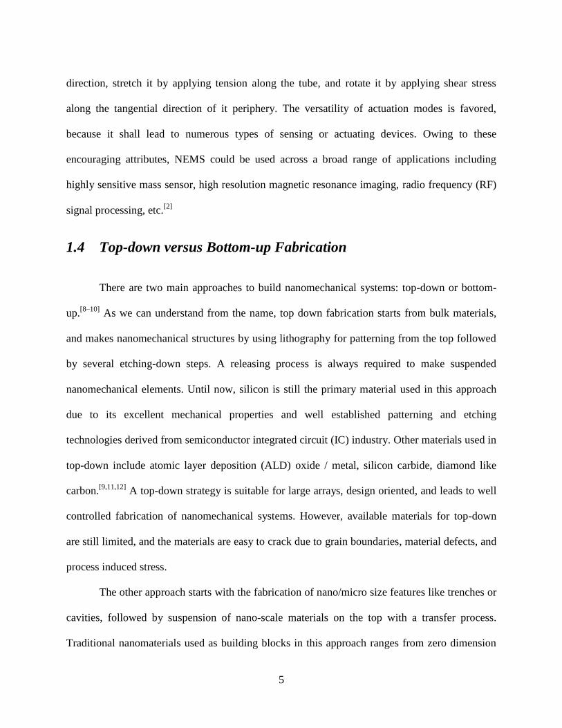
a b
Figure 1.1 Nanomechanical Systems: a) NEMS resonator from exfoliated graphene,[7]
b)
nanomechanical mass sensor to detect molecules (adapted from http://the-briefing.com).
5
direction, stretch it by applying tension along the tube, and rotate it by applying shear stress
along the tangential direction of it periphery. The versatility of actuation modes is favored,
because it shall lead to numerous types of sensing or actuating devices. Owing to these
encouraging attributes, NEMS could be used across a broad range of applications including
highly sensitive mass sensor, high resolution magnetic resonance imaging, radio frequency (RF)
signal processing, etc.[2]
1.4 Top-down versus Bottom-up Fabrication
There are two main approaches to build nanomechanical systems: top-down or bottom-
up.[8–10]
As we can understand from the name, top down fabrication starts from bulk materials,
and makes nanomechanical structures by using lithography for patterning from the top followed
by several etching-down steps. A releasing process is always required to make suspended
nanomechanical elements. Until now, silicon is still the primary material used in this approach
due to its excellent mechanical properties and well established patterning and etching
technologies derived from semiconductor integrated circuit (IC) industry. Other materials used in
top-down include atomic layer deposition (ALD) oxide / metal, silicon carbide, diamond like
carbon.[9,11,12]
A top-down strategy is suitable for large arrays, design oriented, and leads to well
controlled fabrication of nanomechanical systems. However, available materials for top-down
are still limited, and the materials are easy to crack due to grain boundaries, material defects, and
process induced stress.
The other approach starts with the fabrication of nano/micro size features like trenches or
cavities, followed by suspension of nano-scale materials on the top with a transfer process.
Traditional nanomaterials used as building blocks in this approach ranges from zero dimension

6
fullerene or gold particles to one dimensional carbon nanotubes (CNT) or silicon nanowires.[8,13]
The exceptional properties of nanomaterials can be integrated and transferred to the
nanomechanical systems with this approach. However, we can rarely achieve large array
fabrication in this case.
Combining these two approaches, to integrate their advantages and to avoid their
drawbacks becomes an interesting issue in wafer scale fabrication of nanomechanical systems,
nano-electronics, nano-optoelectronics, etc. The ideal strategy should allow large arrays, design
oriented fabrication as well as the integration of nanomaterials with exceptional properties. The
development of 2D materials provides a promising approach to the integration of outstanding
properties from nanomaterials into large arrays of devices. Take graphene for example. Right
now we don’t have to wait for good luck to bring us tens of micron size graphene by drawing
graphite. Instead, it is possible to make graphene wafers with chemical vapor deposition of
carbon atoms on copper foil followed by a transfer process, which can move graphene from the
foil to any substrate we want[14–17]
. In this way, graphene becomes compatible to traditional
microfabrication techniques and even complementary metal-oxide semiconductor (CMOS)
process. Graphene itself, can be patterned by oxygen plasma, which will not etch typical
substrate materials, like Si, SiO2, and metals[18]
. On the other hand, release etchants for SiO2 or
metals does not severely damage the quality of graphene. The compatibility for integration and
the selectivity during fabrication process in graphene and other 2D materials offers the
possibility to fabricate large arrays of nanomechanical/nanoelectronics devices while keeping the
intrinsic properties in the 2D materials.
7
1.5 Conclusion
This chapter introduces the outline of this thesis, followed by a brief introduction of 2D
materials, mechanics in 2D materials, and review of nanomechanical systems in Chapter 2, 3, 4,
respectively. In Chapter 5, we will introduce our novel design of graphene NEMS switches, and
demonstrate our study on the large arrays of 3-terminal switches fabricated. In Chapter 6, we will
describe the measurement of the interfacial forces between graphene and substrate with a unique
set up. Chapter 7 will introduce the electronic bandgap tuning in monolayer MoS2 with biaxial
strain.

8
Chapter 2
Graphene, MoS2, and Beyond
2.1 2D Materials
Dimensionality is one of the most fundamental material parameters, which not only
defines the atomic structure of the material but also determines the properties to a significant
degree.[19–23]
The same chemical element or compound can exhibit dramatically different
properties in different dimensionality. After the discovery of fullerene and single layer carbon
nanotube (CNT), which are 0D and 1D carbon nanomaterials respectively, researchers tried to
isolate 2D graphitic material or to make 1D nano-ribbons from 2D crystals. The efforts have
started to pay off since 2004 with the first isolation and electrical characterization of graphene
transistors published by Geim’s group.[18]
At that time, most people would not expect that more
than a dozen kinds of 2D crystals can be isolated and studied in less than 10 years. Right now,
the 2D materials family includes not just carbon material but also transition metal
dichalcogenides (TMDs), oxides, and layered metals. One of the most promising applications of
2D materials is in electronic devices.[20,21,24]
With respect to the electrical properties, we can
already have superconductors, metallic materials, semimetals, semiconductors, insulators from
the 2D crystals, namely a complete electrical materials family.
Table 2.1 lists all the current members in the 2D layered materials family. However,
stability is a critical issue. The blue shaded materials are stable under ambient conditions (room
temperature in air) for monolayers. Those probably stable in air are shaded green but those may

9
be stable only in inert atmosphere are shaded pink. Grey shading means monolayer has been
exfoliated and verified by AFM, but no further information has yet been provided.
Table 2.1 2D materials family[24]
The rule of thumb to obtain 2D crystal from its 3D layered parent can be helpful for the
search of new 2D family members. First, 3D layered materials with high melting temperature,
typically over 1000 °C, have better chances. Second, potential 3D layered parents better have
chemical inertness. Third, insulating and semiconducting 2D crystals are more likely to be stable
after exfoliation or synthesis. [24]

10
Figure 2.1 Common 2D materials: graphene, MoS2, hBN, WSe2, and Fluorographene.[24]

11
2.2 Graphene
Even though graphene is the last one to be isolated in the carbon materials family, it
serves as the building block for other family members with different dimensionalities. It can be
wrapped up into 0D buckyballs, rolled into 1D nanotubes or stacked into 3D graphite.[22,24,25]
Furthermore, graphene exhibits a combination of excellent electronic[25–27]
, mechanical[28,29]
,
optical[30]
and thermal properties[31]
, which may make it substitute silicon in electronics,
photonics, and NEMS as well in this century or next, and this is most researchers’ “dream” about
graphene or other 2D materials. Considering graphene as a structural material used in NEMS,
here I will briefly introduce the electronic and mechanical properties.
Graphene was initially discovered as a remarkable high quality semimetal with a
pronounced ambipolar electric field effect.[18]
Charge carriers in the material can be tuned
continuously between electrons and holes in concentration as high as 1013
cm-2
and their mobility
can exceed 15,000 cm2V
-1s
-1 under room temperature and with a SiO2 substrate underneath.
Besides, as its allotrope-diamond, graphene is considered one of the stiffest and strongest
materials if it is in the form of single crystal. Its Young’s modulus for stretching is as high as 1
TPa, and breaking stress about 42 N/m with 25% strain, thereby showing the potential of fast
response and long life cycle without failure in NEMS.[28,29]
What is more, graphene is
impermeable to gas molecules, and even helium atoms cannot pass through.[32]
This highly
conductive, strong and flexible, gas impermeable membrane attracts great interests to make
NEMS out of graphene.[32]

12
a
bc
d
Figure 2.2 Electrical and mechanical properties in graphene a) Ambipolar electric field effect in
single-layer graphene.[22]
b) (lower) SEM images of the suspended CVD graphene film over
holes. (upper) Schematics of the device. c) Force-displacement curve of the single grain
graphene film in AFM nanoindentation. Insets are AFM images of graphene film before and
after nanoindentation. Scale bar is 3 μm and 1 μm for (b) and (c), respectively.[28]
d) AFM
images of gas impermeable graphene membranes when bulged down (upper) and bulged up
(lower).
13
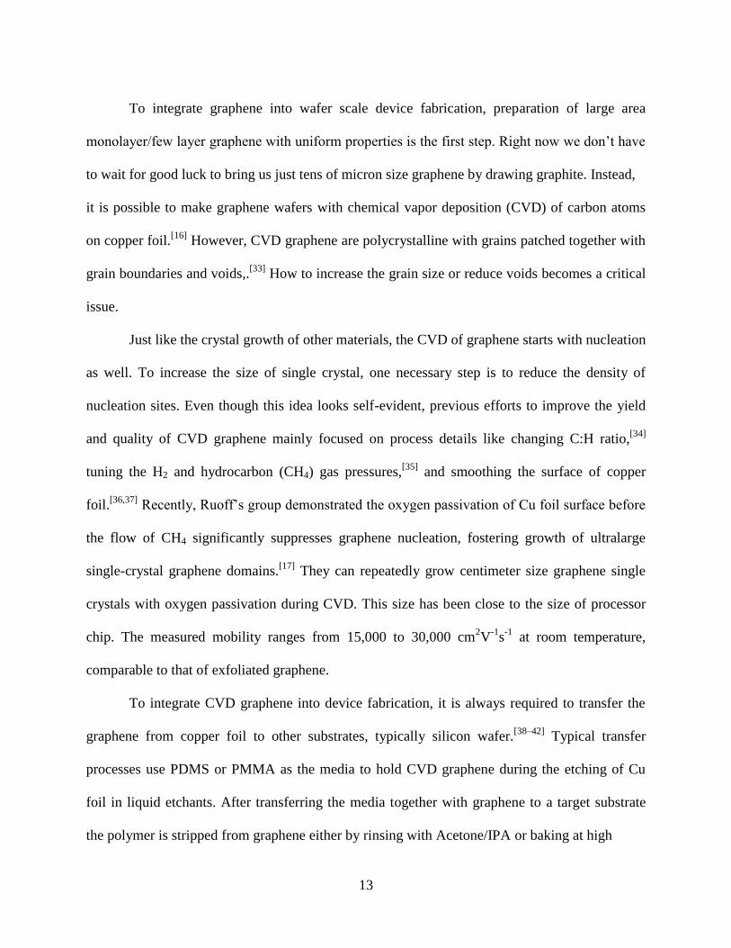
To integrate graphene into wafer scale device fabrication, preparation of large area
monolayer/few layer graphene with uniform properties is the first step. Right now we don’t have
to wait for good luck to bring us just tens of micron size graphene by drawing graphite. Instead,
it is possible to make graphene wafers with chemical vapor deposition (CVD) of carbon atoms
on copper foil.[16]
However, CVD graphene are polycrystalline with grains patched together with
grain boundaries and voids,.[33]
How to increase the grain size or reduce voids becomes a critical
issue.
Just like the crystal growth of other materials, the CVD of graphene starts with nucleation
as well. To increase the size of single crystal, one necessary step is to reduce the density of
nucleation sites. Even though this idea looks self-evident, previous efforts to improve the yield
and quality of CVD graphene mainly focused on process details like changing C:H ratio,[34]
tuning the H2 and hydrocarbon (CH4) gas pressures,[35]
and smoothing the surface of copper
foil.[36,37]
Recently, Ruoff’s group demonstrated the oxygen passivation of Cu foil surface before
the flow of CH4 significantly suppresses graphene nucleation, fostering growth of ultralarge
single-crystal graphene domains.[17]
They can repeatedly grow centimeter size graphene single
crystals with oxygen passivation during CVD. This size has been close to the size of processor
chip. The measured mobility ranges from 15,000 to 30,000 cm2V
-1s
-1 at room temperature,
comparable to that of exfoliated graphene.
To integrate CVD graphene into device fabrication, it is always required to transfer the
graphene from copper foil to other substrates, typically silicon wafer.[38–42]
Typical transfer
processes use PDMS or PMMA as the media to hold CVD graphene during the etching of Cu
foil in liquid etchants. After transferring the media together with graphene to a target substrate
the polymer is stripped from graphene either by rinsing with Acetone/IPA or baking at high

14
a b
Cc d
e
Figure 2.3 CVD growth and transfer of graphene a) SEM image of low-density graphene
domains on OR-Cu exposed to O2.[17]
b) Optical image of centimeter-scale graphene domains on
OR-Cu exposed to O2. c) The graphene nucleation density vs O2exposure time. d) Plots of
resistivity and conductivity as a function of gate voltage at 1.7 K. e) Dry transfer of CVD
graphene over microcavities using PDMS.

15
temperature for PMMA, or by directly peeling PDMS. In this way, graphene becomes
compatible to CMOS processes. Graphene can be patterned by oxygen plasma, which will not
etch typical substrate materials, like Si, SiO2, and metals. On the other hand, release etchants for
SiO2 or metals can hardly impair the quality of graphene significantly. The compatibility for
integration and the selectivity during fabrication process offers great flexibility for the
fabrication of graphene based NEMS or other electronic, photonic devices.
2.3 MoS2
The intense interest and rapid progress in graphene researches also led to exploration of
other 2D materials.[10,20,23]
In particular, single layers of transitional metal dichalcogenides
(TMDs) have attracted notable attention because of their diverse properties and natural
abundance. Despite the similarity in the chemical formula MX2, where typically M is a transition
metal of groups 4-10 and X is a chalcogen, single layer 2D TMDs exhibit versatile chemistry and
properties, ranging from insulators such as HfS2, semiconductors such as MoS2, semimetal such
as TiSe2, to true metals such as NbS2, which can even exhibit superconductivity at low
temperature.
One important reason for researchers to study TMDs single layers is to find
semiconductors with sizable band gaps, therefore we can apply this kind of materials in field
effect transistors (FETs) to achieve improved on/off ratio compared with graphene FETs, or use
them as light-absorbing materials in alternative thin film solar cells considering their bandgaps in
the visible range.[10]
Here we will just introduce MoS2 as a representative of TMDs, since it has
been the most studied so far due to its natural abundance and ease of exfoliation from a parent
3D crystal.

16
a
c d
b
Figure 2.4 a) Atomic structure of monolayer MoS2.[10]
b) Optical image of exfoliated monolayer
MoS2 flake. c) Optical image of CVD MoS2 flake. d) Simplified band structure of bulk MoS2.[43]
a
dc
b
Figure 2.5 a) Schematic of MoS2 top gate field effect transistor. b) Ids vs Vg.[44]
c) Schematic of
MoS2 photodetector. d) Photoresistivity over illumination wavelength. [45]
17
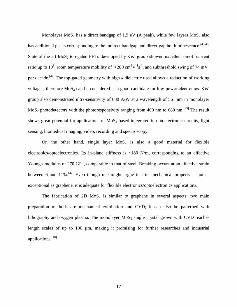
Monolayer MoS2 has a direct bandgap of 1.9 eV (A peak), while few layers MoS2 also
has additional peaks corresponding to the indirect bandgap and direct-gap hot luminescence.[43,46]
State of the art MoS2 top-gated FETs developed by Kis’ group showed excellent on/off current
ratio up to 108, room temperature mobility of >200 cm
2V
-1s
-1, and subthreshold swing of 74 mV
per decade.[44]
The top-gated geometry with high k dielectric used allows a reduction of working
voltages, therefore MoS2 can be considered as a good candidate for low-power electronics. Kis’
group also demonstrated ultra-sensitivity of 880 A/W at a wavelength of 561 nm in monolayer
MoS2 photodetectors with the photoresponsivity ranging from 400 nm to 680 nm.[45]
The result
shows great potential for applications of MoS2-based integrated in optoelectronic circuits, light
sensing, biomedical imaging, video, recording and spectroscopy.
On the other hand, single layer MoS2 is also a good material for flexible
electronics/optoelectronics. Its in-plane stiffness is ~180 N/m, corresponding to an effective
Young's modulus of 270 GPa, comparable to that of steel. Breaking occurs at an effective strain
between 6 and 11%.[47]
Even though one might argue that its mechanical property is not as
exceptional as graphene, it is adequate for flexible electronics/optoelectronics applications.
The fabrication of 2D MoS2 is similar to graphene in several aspects: two main
preparation methods are mechanical exfoliation and CVD; it can also be patterned with
lithography and oxygen plasma. The monolayer MoS2 single crystal grown with CVD reaches
length scales of up to 100 µm, making it promising for further researches and industrial
applications.[48]

18
2.4 Conclusion
This chapter has a general introduction of 2D materials and introduces the electrical and
mechanical properties of graphene and MoS2 in detail. The next chapter will describe the
nanomechanics of 2D materials which will be applied for the analysis of the experimental parts
of this thesis.

19
Chapter 3
Nanomechanics of 2D Materials
3.1 Mechanical Properties of Membranes
The most fundamental mechanical properties of engineering materials lie in the linear
response of strain under stress, also known as Hooke’s Law, which can be considered a
mechanical equivalent to Ohm’s law. If we apply a uniaxial compressive or tensile stress to the
material, the relation can be expressed as:
σ = Eε (3. 1)
where σ stands for the stress, while ε the strain. Materials usually differ from each other in E,
known as the modulus of elasticity of Young’s modulus.[19,49]
When applying shear loading to the material instead, we can write a similar equation:
τ = Gγ (3. 2)
where τ and γ are the shear stress and strain, respectively; G is called the shearing modulus of
elasticity or modulus of rigidity of the material.
Another unique property in different materials is related to the geometry of the material,
Poisson’s ratio ν, which is the constant ratio of the lateral strain to the axial strain. However, G is
related to E and ν as in an isotropic material:
( )
(3. 3)
Accordingly, there are only two independent elastic constants.

20
In practice, materials are usually engineered into different types of structures, like 1D
bars or frame structures. Planar or curved structures are a family of structures that have two
dimensions much larger than the third one. Three family members are included in the third type:
panel, plates and shell. Panels are loaded only to in-plane stress, while plates are subjected to out
of plane loads as well. Shells are usually curved planar structures with very small thickness
compared with their other dimensions, which can only resist tensile and compressive forces.[50,51]
In this thesis, we focus on the membranes, which are identified as a special kind of shell
incapable of conveying shear loads. In other words, bending can be ignored in membranes. To
further understand the mechanics in membranes, we can consider a part of a spherical shell of
radius R and thickness t, under a uniform pressure of P. The compressive direct stress is
(3. 4)
The shell bending moment is
(3. 5)
So, the bending stress is given by
(3. 6)
We can derive the ratio of the direct stress to the bending stress
(3. 7)
Therefore, we can ignore the bending stress if the in plane stress is much greater than the
bending stress as (t/2r) << 1. In 2D membranes, t is the atomic thickness with a few angstroms
and r is usual of micron size, leading to the ratio between 103 and 10
4. Hence, we assume the
bending stress is negligible in the 2D membranes.
21
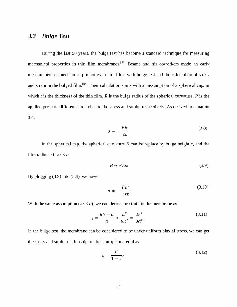
3.2 Bulge Test
During the last 50 years, the bulge test has become a standard technique for measuring
mechanical properties in thin film membranes.[52]
Beams and his coworkers made an early
measurement of mechanical properties in thin films with bulge test and the calculation of stress
and strain in the bulged film.[53]
Their calculation starts with an assumption of a spherical cap, in
which t is the thickness of the thin film, R is the bulge radius of the spherical curvature, P is the
applied pressure difference, σ and ε are the stress and strain, respectively. As derived in equation
3.4,
(3.8)
in the spherical cap, the spherical curvature R can be replace by bulge height z, and the
film radius a if z << a,
R a2/2z (3.9)
By plugging (3.9) into (3.8), we have
(3.10)
With the same assumption (z << a), we can derive the strain in the membrane as
(3.11)
In the bulge test, the membrane can be considered to be under uniform biaxial stress, we can get
the stress and strain relationship on the isotropic material as
(3.12)

22
For the simplest case of an initially flat, unstressed membrane, we can have the pressure-
displacement relationship for an elastic material by combining (3.8), (3.11) and (3.12),
( )
(3.13)
When there is an initial tension So on the membrane, where tension is defined as S = σt, becomes
( )
(3.14)
Hencky first developed an analytical solution for the bulge test culminating a relationship
between pressure difference across the membrane and the maximum deflection of the bulge.[54,55]
The analysis starts with the equations in their axisymmetric form for circular membranes are as
follows,
(3.15)
( )
(3.16)
Here, and are radial and tangential components of the membrane stress respectively, r is
the radial coordinate, p is the pressure load acting on the membrane, and w is the deflection. The
membrane stresses are related to their respective membrane strains and through
( )
(
)
(3.17)
( )
(3.18)

23
where u is radial displacement, and equations (3.15) through (3.18) can be reduced to one single
equation in given by
(
)
(3.19)
Then Hencky gave a series solution to (3.19) for clamped circular membranes. He
assumed that the solution to this equation follows the form
(
)
∑ (
)
(3.20)
where, ao is radius of the circular region of the membrane being pressurized, A2n is nth
coefficient. By plugging (3.20) into (3.8) and equating terms on the left hand side with those on
the right hand side in the resultant algebraic equation, he got
etc. The boundary condition of u = 0 at r = a0 gives . Once an approximate
description of the radial stress is obtained, it is easy to obtain the relation between the maximum
deflection and pressure difference across membrane
( ) (
)
(3.21)
where C1 is a constant. Or, we can express the equation as
(3.22)
Similarly, with an initial tension, So, the equation further becomes
(3.23)

24
For 2D membranes, since t is very small, the second term dominates when the deflection
is small.
3.3 Contact Adhesion
Contact adhesion is an essential mechanical property of 2D materials and an interesting
area of study. Due to their atomic thickness and resulting incomparable flexibility, 2D
membranes can conform to the contacting surface much better than bulk materials, thereby
increasing the contact area and adhesion significantly. The measured contact adhesion energy on
graphene is comparable to that of a liquid-solid interface.[56,57]
The ultrastrong contact adhesion
also plays an important role in the 2D materials and devices from them, especially
nanomechanical devices.[58]
Take the NEMS switches as an example: the adhesion can help the
membrane self-clamp over the trenches or cavities, which helps simplify the fabrication process;
on the other hand, a restoring force in the device, determines the required actuation electrical
voltage, and needs to overcome the contact adhesion between 2D membranes and the underneath
electrodes. This is necessary to guarantee repeatable switching. Therefore, the ultrastrong contact
adhesion can result in an undesirably high actuation voltage for the device to repeatedly switch.
How to make a reliable NEMS switches with low actuation voltage requires the development of
approaches to decrease the contact adhesion force.
3.4 Blister Test
Other than traditional methods to measure the contact adhesion in thin films/membrane,
including peel test, pull test, and scratch test, the blister test turns out to be a widely used
approach to probe the adhesive property, especially in 2D membranes, due to the ease of

25
implementation and film preparation.[55,56,59–61]
The standard spherical blister test has the same
configuration as that used in bulge test, but when the pressure difference across the member is
greater than a critical value the membrane starts to delaminate from the substrate. Recently,
Steven Koenig et al. used a constant N (# of gas molecules) spherical blister test to achieve stable
delamination between graphene and SiO2 substrate and the adhesion energy is calculated using a
thermodynamic model to be 0.45 Jm-2
.[56,58]
Narasimha Boddeti et al. applied constant N island
blister test to get stable and unstable delamination of graphene from SiO2 substrate, and the
adhesion energy measured is comparable, though slightly lower ~ 0.1 Jm-2
.[62]
3.5 Van der Waals Force
The free energy of van der Waals interaction between a monolayer atomic membrane and
a substrate can be derived by integration of pairwise potential energy for the atom-atom
interaction based on Hamaker summation method.[63,64]
The Lennard-Jones potential for the pair-
wise interaction between one atom on the membrane and a substrate atom is
( )
(3.24)
where C1 and C2 are the constant for the attractive and repulsive interactions respectively, while r
is the distance between the atoms. By summing up the atom-atom potential for all the atoms in
the membrane, we have the monolayer-substrate interaction energy, namely
(3.25)
Assuming the substrate has a flat surface while the monolayer membrane is flat as well,
and they are in parallel, then we can get the analytic form of the interaction potential between the
membrane and the substrate,
26
[
( )
( )
] (3.26)
where UvdW is the monolayer-substrate interaction energy per unit area, z is the distance between
the monolayer and the substrate surface, is the equilibrium separation, and is the adhesion
energy at the equilibrium separation.[65]
Accordingly, the van der Waals interaction can be obtained by taking the derivative of
the interaction over z,
[( )
( )
] (3.27)
As an approximation, we can consider the attractive van der Waals interaction between a
flat monolayer membrane and a flat substrate in unit area as this form
(3.28)
3.6 Electromechanical Actuation
Electromechanical actuation with electrostatic force is one of the most common ways to
deflect or vibrate micro/nano mechanical structures.[66,67]
When applying a voltage V on a
capacitor, composed of a micro/nano mechanical structure and a gate electrode for example, the
energy stored in the capacitor is
(3.29)
where C is the capacitance. The induced electrostatic force is
(3.30)

27
For capacitors with parallel plates, we have the electrostatic pressure as
(3.31)
where is the dielectric permittivity of vacuum space, is dielectric constant for the
intermediate material.
3.7 Pull in Phenomenon
When we mention “pull in” or “snap through” phenomenon, we always think of the pull
in instability in the parallel plate electrostatic actuators, where the actuator gets unstable and
collapses at 1/3 of the original distance between the plates. In principle the instability occurs
when the rate of change in voltage vs deflection distance is zero during electrostatic actuation.
The 1/3 rule can be applied to electrostatic actuators in the form of cantilever, doubly clamped
beam, or piston parallel plate.[66,68]
Similarly, the pull in instability in 2D membranes happens when the rate of change of
pressure difference across the membrane vs deflection h equals to zero.[69]
(3.32)
Here, is not limited to the pressure difference from the input gas across the membrane,
but can be combined with the pressures from electrostatic force, interfacial forces, etc.
3.8 Conclusion
This chapter review relevant nanomechanics in 2D materials for the experimental
sessions. Next chapter includes a review of nanomechanical systems in terms of NEMS switches,
measurement of interfacial forces, and strain engineering with 2D materials.

28
Chapter 4
Nanomechanical Systems: Review of NEMS Switches,
Interfacial Forces and Strain Engineering
4.1 Nanoelectromechanical switches
The development of nanotechnology makes us reexamine one interesting idea -
mechanical computing, which was proposed by Charles Babbage about two centuries ago. This
idea was completely overwhelmed by the soaring progress in micro/nanoelectronics, which can
be represented by Moore’s law in last forty years postulated by Gordon Moore in 1965. It
predicted that by scaling down the size of transistors, the number of transistors on a chip would
roughly double every 18 months [22]
. However, when we ultimately reach the scaling limit of
semiconductor transistor, it might be time to reinvent the transistor [70]
. A NEMS switch is one
promising candidate.
As mentioned, the resonance frequency of NEMS can reach up to 10 GHz, thereby
making NEMS based electromechanical computers potential viable alternative to work at an
even faster speed than state of the art computers in the current market. NEMS switches can also
have a low off-state current limited by Brownian motion and tunneling and high on/off ratio,
which are great barriers for traditional semiconductor transistors when scaling down to tens of
nanometers. Therefore, by means of mechanical computing with NEMS switches we could solve
these problems, thus decreasing the power consumption for computing due to leak currents.

29
Another attractive attribute for NEMS switches is “harsh environment robustness”, namely high
temperature resistance and radiation hardness. Different from conventional semiconductor
transistors, which function based on the electronic properties of semiconductor materials and
interfaces, NEMS switches work with mechanical movement. The harsh environments, like high
temperature and radiation, can easily affect the interfaces in semiconductor transistors but hardly
influence the mechanical movement of nanostructures in NEMS. In sum, NEMS switches are
capable of achieving virtually microwave operating frequencies, zero off-state current, high
temperature resistance, and radiation hardness. These are attractive advantages over existing
complementary metal-oxide semiconductor field-effect transistors.
4.1.1 Graphene Based NEMS Switches
Carbon based nanomaterials including fullerene, graphene and carbon nanotube (CNT)
have resulted in two Nobel Prizes and are considered as one of the most attractive elementary
materials in the nano world due to their incredible properties in mechanical, electrical, thermal,
and even biological fields. Here, I will review the NEMS switches from graphene and CNT,
which are the 2D and 1D carbon materials, respectively.
The first graphene NEMS switch was developed by Jing Kong’s group in MIT[71]
. The
device was fabricated by deposition of two layers of graphene separated by a 500 nm gap. The
top layer was etched into a 3 µm wide strip suspended over a 20 µm wide trench, and it can
deflect and contact the bottom layer by applying ~5 V voltage between them. The schematic and
SEM image of the device is shown in Figure 4.1. This first NEMS switch from graphene
functioned unreliably, and failed due to tears on CVD graphene after several times of switching.

30
a b
c d
Figure 4.1Graphene NEMS switches a) Schematic diagram of an all CVD graphene switch from
a cross sectional view and a top view. b) SEM images of suspended graphene and tear on
graphene.[71]
c) Schematic of the 3-terminal graphene switches with a STM probe. d) SEM image
of the device.[72]

31
Kang Wang’ group improved the fabrication, and suspended a strip of CVD graphene
over a smaller trench of 20 µm width and 150 nm depth[73]
. This graphene switch can work at
actuation voltages of 1.85 V, which is compatible with conventional complimentary metal-oxide-
semiconductor (CMOS) circuit requirements. They also reported abrupt on/off characteristic,
demonstrating fast response from the device.
G. Zhang’s group tried to make a three terminal graphene switch from exfoliated
graphene using a similar geometry as previous devices but with a 100 nm wide gold electrode
patterned by e-beam lithography in a 2 μm x 0.15 μm trench[72]
. However, the switches with this
geometry suffered restoring failure due to a strong van der Waals force when graphene touches
the electrode even though the electrode is only 100nm wide. They also designed a multilayer
graphene NEMS switch with a “point” contact based on their studies on the former graphene
NEMS switches. Through quantitative study of the vdW force on graphene and restoring force
by sticking and unsticking graphene with an AFM tip, they realized the monolayer graphene
device will not recover unless the gold wire width is less than 5nm. They also studied the
mechanical robustness of monolayer graphene, and found the monolayer is easy to tear making it
not as good as multilayer graphene for NEMS switches. Therefore, “point” contact graphene
NEMS switches from multilayer shows potential for greater reliability. Instead of a gold wire as
the drain electrode, they used an STM probe with contact area ~150 nm2, which can lead to ~60
nN probe-graphene vdW force, reflected by the 15 V threshold voltage. The point switch can
work over 500 cycles, the most ever reported.
Different from the mechanism of the switches with doubly clamped beam structure,
graphene switches developed by Marc Bockrath’s group operate based on the formation and
breaking of carbon atomic chains that bridge the graphene break junctions[74]
. Geometrically, it is

32
a d
cb
e
Figure 4.2 a) SEM image showing the breakdown of graphene. b) Electrical measurement
showing the breakdown of graphene. c) Electrical measurement of graphene atomic switch. d)
Schematic showing the atomic switching of the device.[74]
e) The SEM images of ON and OFF
state for the atomic switch with suspended graphene. The scale bar is 1 μm.[75]

33
like a lateral switch. The switches are fabricated by creating nanoscale gaps using electrical
breakdown of graphene sheets-a reliable self-limiting process that avoids the need for advanced
lithographic technique. Applying appropriate bias voltage pulses switches the gap conductance
between high (ON) or low (OFF) conductance states.
Figure 4.2a shows an SEM image of a graphene switch after the formation of a break
junction by a voltage pulse of 1.5 V. The breaking down of the graphene sheet is also supported
by the IV curve, which is shown in Figure 4.2b. After the voltage increases to 1.5 V, the current
decreases suddenly which indicates the breaking of the graphene sheet. After the fabrication of
the device with a broken junction, when the voltage is smaller than 2 V, the current is very low;
when it reaches ~2.5 - 4 V, the current abruptly increases, reaching a maximum of 0.65 mA at
~5 V. However, with further increase of voltage, the conductance returns to its initial low-
conductance state. A typical switching IV curve is shown in Figure 4.2c. They proposed a model
for the switch, which claims the devices switch on and off by alternative formation of carbon
atomic chains bridging the breaking junction due to the voltage applied (Figure 4.2d). Therefore,
by applying voltages of different magnitudes, the graphene devices can be switched into ON and
OFF states, thereby functioning as voltage programmable bi-stable switches or memory elements.
To rule out the influence of the substrate, which can also bridge the breaking gap
electrically, they also fabricated suspended atomic switches from graphene[75]
. Interestingly, the
graphene cantilevers after the breaking process can stay suspended considering their low bending
rigidity. Furthermore, the graphene break junction switch on/off similar to those staying on
silicon oxide substrates.

34
a b
c d
e
Figure 4.3 a) (A through E) Dark-Field optical micrographs of the nanotube arms at potentials of
0, 5, 7.5, 8.3, and 8.5 V, respectively. Scale bars, 1 mm. b) Dark-field optical micrographs
showing the sequential process of nanotweezer manipulation of polystyrene nanoclusters
containing fluorescent dye molecules.[76]
c) A schematic illustration of the CNT-based
electromechanical switch device. d) SEM image of the device: The length and diameter of the
MWCNTs are about 2 μm and 70 nm, respectively. e) Current-voltage characteristics of
switching action in an ambient environment; the electromechanical movement of MWCNTs
provides the on and off states. The scale bar corresponds to 1 μm. [77,78]

35
4.1.2 Carbon Nanotubes Based NEMS switches
A CNT can be considered a more complicated form of carbon where a strip of graphene
is wrapped into a tube shape. However, CNTs were discovered several decades earlier than
graphene, and CNTs were applied into NEMS about one decade earlier. As a 1D material, CNT
demonstrates different mechanical properties from graphene. Prominent of them is a
considerable bending rigidity, which makes cantilevers of CNT be promising structures for
NEMS switches as well.
CNT nano-tweezers reported by Philip Kim and Charles Lieber is one example of the
earliest CNT based cantilever switches[76]
. It is fabricated by attaching two CNT to independent
electrodes fabricated on pulled glass micropipettes. Similar to tweezers used in daily life, the
CNT nanotweezers can grab and manipulate submicron clusters and nanowires. It works by
deflecting the two CNT cantilevers actuated by electrostatic force between them. Different from
typical MEMS/NEMS with only one movable part for one device, both CNT cantilevers can
deflect. Reported actuation voltage is ~8.5V.
Based on the work on nanotweezers, Jang from Amaratunga’s group demonstrated
NEMS switching from a similar device[77]
. Vertical CNTs cantilevers are grown in situ on Ni
catalyst dots via a CVD bottom-up process. In this way, large arrays of device fabrication and
integration become feasible. The original device reported in 2005 had a pull-in voltage of ~24 V,
but decreased down to ~4.5 V after improvements[78]
. This kind of CNTs vertical cantilever
NEMS switches show great potential as mechanical transistors, logic devices, and non-volatile
memory cells, and RF NEMS applications.
S. W. Lee et al. demonstrated three terminal NEMS switches from multiwall CNTs
(MWNTs) in a horizontal geometry instead. The device switches by deflecting the CNT

36
a b
c
d
e
f
Figure 4.4 a) Schematic diagram of the carbon nanotube relay, b) IV characteristics of a
nanotube relay initially suspended approximately 80 nm above the gate and drain electrodes. Vsd
= 0.5 V.[79]
c) Schematic of the device. d) SEM image of the device. e) IV characteristic of the
device. f) Response time measurement showing the response time equals 2.8 ns.[80]

37
cantilever with a gate voltage to contact the drain electrode. I-Vsg characteristics of a nanotube
relay initially suspended approximately 80nm above the gate and drain electrodes showed a
nonlinear increase of current as the gate voltage increased when Vsg < 20 V, but the linear current
increase and strong fluctuations are seen for Vsg > 20 V. The Vsd was 0.5 V. They observed some
hysteresis effect on the restoring of CNTs when decreasing the gate voltage, which might be
utilized for nonvolatile memory applications.
When clamped on both ends, the CNT can exhibit higher tension after deflection, thereby
increasing the restoring force and response rate. A.B. Kaul et al. studied the switching speed of
the doubly clamped NEMS switches from single walled nanotubes (SWNTs), and showed that
the CNT switches measured to be 3 orders of magnitude faster than MEMS switches, with a
switching time of 2.8 ns while requiring pull-in voltages less than 5 V[79]
. Some other researchers
also used arrays of horizontally aligned CNTs for NEMS switches, which show similar switching
properties[81,82]
.
4.1.3 Thin film lateral NEMS Switches
The other major way to make NEMS is to etch traditional MEMS material like single
crystal or poly silicon into submicron thin film movable structures, and switch them laterally
over tens of nanometer gaps by electrostatic force. It is a lot easier to fabricate wafer scale
arrays of devices and to integrate into complementary metal oxide semiconductor integrated
circuits (CMOS IC) with this method than application of nanomaterials (CNTs or graphene),
even though the submicron structures can hardly be scaled down further due to the decay of
mechanical robustness by defects.

38
a
b c
d e
Figure 4.5 a) Layout design of the lateral switch, b) SEM image of the device, c) IV
characteristic of the device.[83]
d) & e) SEM image of SiC NEMS inverter.[11]

39
One of the earliest examples is a Ruthenium thin film NEMS switches developed by
David. A. Czaplewski et al[83]
. A layer of 200 nm thick ruthenium film is deposited by sputtering
(210 W DC power, 50 W substrate bias, 4.6 mTorr, 25°C). The Ruthenium thin film is etched by
high density plasma RIE (15 mTorr, 10 sccm Cl2, 90 sccm O2, 500 W upper power, 200 W lower
power) into designed shape with a 50 - 100 nm wide and 3 - 10 μm long beam separated from
gate electrode with 30 – 100 nm, and drain electrode 20 - 70 nm masked by a layer of PECVD
SiO2. A typical switch can pull in at ~5 V with a measured switching time of ~400 ns. The
maximum lifetime measured is approximately two million cycles tested at a 1 kHz cycle
frequency. Furthermore, all processing in the fabrication is CMOS compatible.
T Lee from M. Mehregany’s group developed SiC NEMS switches operating at 500°C, at
which the mature silicon FET technologies fail due to excessive leakage caused by p-n
degradation and thermoionic leakage. Heavily nitrogen-doped (ND ~ 1x10²⁰
cm-3
) polycrystalline
3C-SiC films are deposited on the silicon wafer[11]
. Assembling two SiC NEMS switches
together, they made an inverter, a fundamental element for electromechanical computing. The
length, width, and actuation gap of the cantilevers are ~8 μm, ~200 nm, and 150 nm, respectively.
Typical switches measured have operated ≧21 billion cycles at 25 °C and ≧2 billion cycles at
500 °C.
Howe’s group at Stanford is working on the polysilicon lateral NEMS. About 1.2 μm
thick polysilicon with 50 nm sputtered platinum is used as the thin film for movable beam and
electrodes. They designed a strategy to separate the mechanical and electrostatic domains,
yielding individual control of the pull-in voltage and electrode displacements, enabling the
device to be more robust against the shorting of the beam to gate[84]
. They realized that an
electrically connected beam and drain has several drawbacks, cascading these three terminal
40
lateral switches, necessary for digital circuits, requires the sustainable voltage across the contact
to be greater than or equal to the pull-in voltage. To solve the problem, they add a DC bias
electrode that partially actuates the beam towards the drain and isolating the beam to form a
conductive channel that connects the source and drain electrodes when the relay is in the ON
state[85]
.
4.1.4 NEMS memories
The consumer electronics industry is rapidly transitioning to mobile electronics from the
dominance of mature home electronics. The uprising of smart phones is the most obvious
example of electronic gadgetries that are filling consumers’ pockets. Flash memory has enabled
the widespread use of these mobile devices by providing storage for the increasing amount of
user data that must be carried[86]
.
Current memory technologies, such as DRAM, SRAM, and NAND flash, are
approaching very difficult issues related to their continued scaling to and beyond the 16nm
generation[87]
. Fortunately, research over the past ten-fifteen years has led to discovery of several
new memory technologies, holding the promise for further continuing scaling. These emerging
research memory technologies include the Ferroelectric-gate FET, NEMS RAM, Nanowire
phase change memory, electronic effects memory (ie. Charge trapping, mott transition,
ferroelectric barrier effects), macromolecular and molecular memory, and nanoionic or redox
memory (including the fuse/antifuse memory and related electrochemical metallization,
programmable metal cell and the atomic switch)[87]
. As one recognized promising memory
technology, NEMS nonvolatile memory has a host of advantages, such as high response speed
due to high resonance frequency, low power consumption due to small size, harsh environment
41
operation due to the switching mechanism of mechanical movements. The potential density of
thin film NEMS reaches up to 1012
elements/cm2.
T. Rueckes et al. proposed a CNT based nonvolatile random access memory for
molecular computing[13,87]
. In their design, each memory element is based on a suspended,
crossed nanotube geometry that leads to bistable, electrostatically switchable ON/OFF states.
Bistability can be envisioned as arising from the interplay of the elastic energy, which produces a
potential energy minimum at finite separation, and the attractive van der Waals energy, which
creates a second energy minimum when the suspended SWNT is deflected into contact with the
lower nanotube. An element could be switched between well-defined OFF and ON states by
transiently charging the nanotubes to produce attractive and repulsive electrostatic forces. The
ON/OFF information at an element thus can be read easily by measuring the resistance of the
junction and moreover, can be switched between OFF and ON states by applying voltage pulse at
electrodes n and m. This approach suggests a highly integrated, fast and macroscopically
addressable nonvolatile random access memory (RAM) structure that could overcome the
fundamental limitations of semiconductor RAM in size, speed, and cost. From the calculation,
the minimum magnitudes of the voltages required for switching ON and OFF are 4.5V and 20V,
respectively.
4.2 Theories and Measurements of van der Waals Forces in
Nanomechanical Systems
Van der Waals bonding is considered as a secondary bonding compared to primary ones
such as ionic bonding, covalent bonding, and metallic bonding[49]
. This secondary bonding force
arises from atomic or molecular dipoles, which instantaneously exist whenever there is some

42
separation of positive and negative portions of an atom or molecule. In essence, the bonding
force therefore results from the columbic attraction between the positive end of one dipole and
the negative region of an adjacent one.
Van der Waals force is a universal force, acting between all atoms and molecules, even
between totally neutral ones such as inert gases, carbon dioxide, and hydrocarbons. Accordingly,
it plays a significant role in a host of phenomena like adhesion, surface tension, physical
adsorption, the properties of gases, liquids, gels, and thin films, and the structures of condensed
macromolecules such as proteins and polymers. Van der Waals force analysis is widely
considered in the fields of atomic physics, material science, biomedical engineering, chemistry,
and others[64]
.
4.2.1 Theories on van der Waals Forces
J.D. Van der Waals first introduced intermolecular forces theoretically to explain the
behavior of non-ideal gases in 1873. This kind of force, as we know, was named as van der
Waals force later. London (1930, 1937) first published a satisfactory microscopic theory about
van der Waals force considering it as dipole-dipole interactions between two neutral atoms based
on quantum mechanics considering the perturbation in their zero-point energy, even though the
mechanism of vdW force is much complicated considering many different interactions[88,89]
. By
treating the dipoles as isotropic harmonic oscillators of characteristic frequencies of ω1 and ω2
and polarizabilities α1 and α2, he showed that the potential energy between two dipoles with a
distance d apart as:
(4.1)

43
For the oscillating dipoles, when time taken for the electrostatic field of one
instantaneous dipole to reach the neighboring atom and return is comparable to the fluctuating
period itself, the power law of force changes because the first atom is no longer in phase with its
neighbor atom. This interaction is now known as the retarded van der Waals interaction. Casimir
and Polder (1948) showed that for separations greater than λi/2π, where λi is the characteristic
absorption wavelengths, there is a progressively reducing correlation between the polarizations
of neighboring atoms as distance increases, and the potential energy for two atoms with
polarizabilities α10 and α20 follows,
(4.2)
This equation means that the non-retarded power law changes from 1/d6 to the retarded
1/d7 when the distance d increases above λi/2π
[90]. This power law change effect due to distance
was named as the Casimir-Polder effect.
The limit with two former theories is the ignorance of the influence from neighboring
atoms on the interaction of the pair of atoms. However, the consideration of this effect can make
the problem very complicated, a typical case with quantum mechanics. This problem was solved
with the macroscopic theories, which ignored the atomic structures but consider bulk properties
such as dielectric constants.
Lifshitz, Dzyaloshinskii, and Pitaevskii first put forward a macroscopic theory to obtain
the dispersion force between two flat parallel plates 1 and 2 separated by distance D by a third
medium 3 by applying the methods of modern quantum field theory[91]
. For non-retarded forces,
the force per unit area f follows,

44
∫ ∑
[(
) (
)]
(4.3)
Where εj =εj (iξ) is the dielectric constant (or permittivity) of the jth medium as a function of an
imaginary frequency iξ, and A is the Hamaker constant for non-retarded forces. In the case of
most dielectrics the first term of above equation constitutes about 98% of the total value of f.
For retarded forces, the theory gives
(
) (
) ( )
(4.4)
where ε10, ε20, ε30 are the static dielectric constants, and Φ (ε10, ε20, ε30) is a function whose value
lies between 1 and 69/2π. B is the Hamaker constant for retarded forces.
4.2.2 Early Measurements of van der Waals Force
Early experimental measurements of van der Waals force were done by Derjaguin and his
colleagues in Russia (for example Derjaguin, Lifshitz, and Abrikossova 1956), Sparnaay (1952,
1958), Holland, and Kitchener & Prosser (1957) in Britain[92–94]
. The common point their
methods shared is to position two bodies close together and to measure the force of attraction as
a function of the distance between them. Most measurements carried out at that time were of this
type: the bodies were made of glass or other transparent material, the force was determined by
measuring the deflection of a balanced arm, and the distance between the highly polished
surfaces obtained by optical interference.
The first direct experimental check of the theory of molecular forces of attraction
between condensed bodies was done by Derjaguin’s work in 1957[94]
. Molecular attractions
between quartz-quartz, mixed thallium halide-mixed thallium halide, and chromium-quartz in a

45
range of gap widths from 0.07 to 0.3 microns were measured. The results agreed with the values
derived from Lifshitz’s theory. The best results on glasses are from the Dutch school in Holland
(Black, de Jongh, Overbeek & Sparnaay (1960); Sparnaay & Jochems (1960); Van Silfhout
(1966); Rouweler & Overbeek (1971)). In Rouweler & Oberbeek’s work (1971), the dispersion
force between a fused silica glass lens and a flat in the range 25 to 350 nm were measured[88,92]
.
They observed retardation effect above 50 nm, while at shorter distances a transition towards
non-retarded forces was detected.
There are three main problems with most of those early works:
(1) Electrostatic charges on the surfaces gave rise to spurious results. In some
experiments, forces measured are several orders larger than theoretical values.
(2) When surfaces are so close to each other at the order of 5-20 nm, the impurities like
small dust particles orsilica gel can prevent the measurement at separations smaller than several
tens of nanometers.
(3) Vibrations from the surrounding always found their way into the sensitive moving
parts of the apparatus and could never be completely suppressed.
To solve these problems, Israelachvili measured the van der Waals force using two
crossed cylindrical sheets of muscovite mica, which can be considered molecularly smooth at the
surfaces[88]
. The distance between surfaces was measured to about ±0.2nm precision by allowing
white light to pass through them and observing the interference fringes spectrometrically. The
van der Waals forces were measured by two different methods: (1) by the ‘jump method’, in the
range of 1.5 to 20 nm and (2) by the ‘resonance method’, in the range 10 to 130 nm. The
experimental setup is shown in Figure 4.6a.

46
Upper Mica
Lower Mica
a b
c
Figure 4.6 a) Schematic drawing on the main parts of the apparatus for van der Waals force
measurement. In jump experiments a double cantilever spring was used. In resonance
experiments a single cantilever “bimorph” spring was used. b) 3D rendering of the half mica
cylinders. c) Variation of the power law of the van der Waals force between crossed mica
cylinders with distance D. The curve is based on the combined results of a number of jump and
resonance experiments.[88]

47
The upper glass section is fixed at the end of a double or single cantilever spring. The
lower surface can be moved close to the upper one with a piezoelectric transducer. At some
distance, the two parts will jump into contact (snap in) depending on the stiffness of the spring.
The force can be calculated by the measurement of the jumping distance based on the ‘jump’
(snap in) condition:
(4.5)
Because dx = - dD, this gives the jump distance Do as
(
) ( )
(4.6)
The principle of the resonance method is to measure the resonant frequency fD of the
upper support as a function of the gap distance D, and from this to deduce the law of force in the
range of distances measured. This method allowed relatively accurate measurement of van der
Waals force ranging from 10 nm to 130 nm. From this experiment, Isrealachvili et al. observed
both non-retarded and retarded van der Waals force, and most importantly, they found that the
transition region between them at a distance from ~10 nm to ~100 nm. The result is shown in
Figure 4.6c.
4.2.3 Measurements of van der Waals Force in Micro/Nanomechanical
Systems
Due to the size scaling into submicron and nano region for applications of nano materials,
van der Waals force becomes critically important for the performance and reliability of
MEMS/NEMS devices based on these materials. In MEMS, adhesion (stiction) is a universal
problem affecting the yield and reliability of devices[95]
. The adhesion of the microstructure to

48
adjacent surfaces can occur either during the final steps of the micromachining process (release-
related adhesion) due to the capillary force or after packaging of devices, due to electrostatic
force from over-range input signals or strong van der Waals force or hydrogen bonding. The
versatility of the reasons for adhesion makes it a complicated problem and a huge barrier for the
industrialization of MEMS. Accordingly, adhesion problems became a research focus in the field
of MEMS.
A common experimental technique to examine the surface-surface interaction involved in
silicon microstructures is ‘cantilever beam array (CBA) technique’. A scanning electron
microscope picture of CBA is shown in Figure 4.7a To measure the work of adhesion, the beams
are brought into contact with the underlying substrate. Once the beams make contact with the
underlying substrate, the applied actuation force is removed, and the beams will begin to peel
themselves off the surface. For beams shorter than a characteristic length, their stiffness will be
sufficient to free them completely from the underlying surface. Beams longer than this
characteristic length, however, will remain adhered to the surface. The work of adhesion W,
between two surfaces can be calculated as
(4.7)
where ld is the characteristic detach length of the beams.
Based on the cantilever beam array technique, Delrio & Dunn studied the role of van der
Waals in the adhesion of micromachined surfaces[96]
. They experimentally measure adhesion on
micro-cantilevers ranging from normal vdW to retarded vdW region as a function of surface
roughness, and independently calculated the adhesion using the measured surface topography.
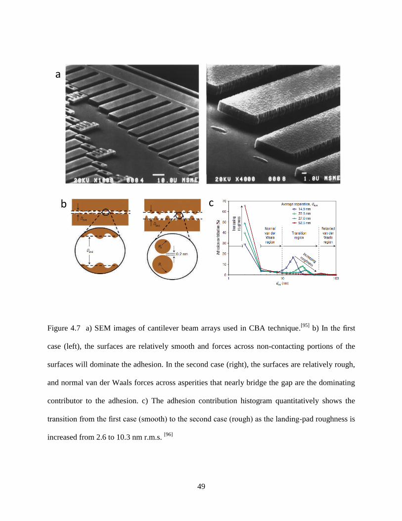
49
a
cb
Figure 4.7 a) SEM images of cantilever beam arrays used in CBA technique.[95]
b) In the first
case (left), the surfaces are relatively smooth and forces across non-contacting portions of the
surfaces will dominate the adhesion. In the second case (right), the surfaces are relatively rough,
and normal van der Waals forces across asperities that nearly bridge the gap are the dominating
contributor to the adhesion. c) The adhesion contribution histogram quantitatively shows the
transition from the first case (smooth) to the second case (rough) as the landing-pad roughness is
increased from 2.6 to 10.3 nm r.m.s. [96]

50
They demonstrated that the adhesion of micromachined surfaces with nanoscale
roughness is in a regime not considered by standard rough surface adhesion models which were
dealing with micro scale roughness. They also showed that the adhesion for surfaces with small
roughness values was mainly due to the van der Waals force acting across extensive non-
contacting areas and is related to 1/D2
avg, where Davg is a result of the planar deposition
technology, while for surfaces with large roughness values, van der Waals forces at contacting
asperities becomes the dominating contributor to the adhesion.
Even before this systematic study of the relationship between van der Waals force and
roughness of microstructure, people have intuitively tried to alleviate adhesion by roughening the
surfaces of microstructure. While some improvements (a factor of 20) were achieved due to
roughening, chemical modification of surfaces showed a better prospect, which can typically
decrease the adhesion energy by a factor of 1000. The basic idea of surface chemical
modification is to change the surface from hydrophilicity to hydrophobicity. Common methods
include hydrogen terminating treatments with Si-H bond for silicon surfaces, self-assembled
monolayers (SAM) coating, diamond-like carbon coating, and fluorocarbon film[95]
.
Van der Waals forces seem always detrimental in MEMS devices because of their
influence on performances and reliabilities, but it is not necessarily true. Chan & Capasso
designed and fabricated a new kind of actuator – a MEMS torsional device actuated completely
by the Casimir force[97–99]
. The results not only demonstrated that this actuation method is
feasible, but also provided one of the most sensitive measurements of the Casimir force between
metalized surfaces. The measurement setup and results are shown in Figure 4.8.

51
a b
c d
Figure 4.8 a) Schematic and SEM image of experimental setup. b) Van der Waals force
measurement results from the experiment.[100]
c) Change in resonance frequency of the oscillator
in response to the electrostatic force and Casimir force as a function of distance. d)Hysteresis in
the frequency response induced by Casimir force on an linear oscillator. [101]

52
Capasso’s group also showed that the Casimir attraction force can influence the
dynamical properties of a micromachined device, changing its resonance frequency and giving
rise to hysteretic behavior and bi-stability in its frequency response to an AC excitation (Figure
4.8c & d), as expected for a nonlinear oscillator[101]
. They also proposed that this device could
serve as a nanometric position sensor.
Without surprise, nanomaterials show a unique property on adhesion from van der Waals
force, similar as other exceptional properties due to size scaling of the material. Compared to
macroscopic and microstructure materials, nano size materials have astonishingly strong
adhesion when contacting substrates, the energy of which are several orders of magnitude larger
than adhesion energies commonly found in Si micromechanical systems.
Koenig & Bunch demonstrated ultrastrong adhesion between exfoliated graphene
membrane and SiO2 substrates by directly measuring delamination pressures of graphene in
blister tests[56]
. The adhesion energy for monolayer graphene is 0.45 ± 0.02 J/m2, and that for
multilayer graphene is 0.31 ± 0.03 J/m2. These values are larger than the adhesion energies
measured in typical micro/nano mechanical structures, and are comparable to solid-liquid
adhesion energies. They attributed these high adhesion energies to the flexibility of graphene,
which allows it to conform to the topography of substrates in a greater degree than traditional
microstructure material, thus making its short range van der Waals interaction much stronger.
Scharfenberg and Zong measured the graphene adhesion as well by exfoliating a piece of
graphene on to substrates with a special topography, namely microsacle - corrugated metallic (Al)
substrates and gold nanoparticles on Si substrate[102]
. By measuring the conformation of
graphene to the features on substrates, they can calculate the adhesion energy between graphene
and the substrates. The adhesion energies they measured are about half of the value measured by

53
a b
c d
Figure 4.9 a) Deflection versus position for five different values of p between 0.145 MPa
(black) and 1.25 MPa (cyan). The dashed black line is obtained from Hencky’s solution for p
~0.41 MPa. The deflection is measured by AFM along a line that passes through the center of the
membrane. b) 1-5 layers Graphene/SiO2 adhesion energies.[56]
c) The normalized to the case of
ideal metals van der Waals and Casimir energy and force (d) per unit area between a graphene
and a semispace versus separation. The solid and dashed lines are related to the semispace made
of Au and Si, respectively. [103,104]
54
Koenig. This difference might come from the use of smaller value of Young’s Modulus in their
calculation. Gao and Huang studied the effect of surface roughness analytically on adhesion of 1-
10 layers of graphene membranes based on Koenig’s experiment. For monolayer graphene, the
influence of roughness is extremely mild with the corrugation amplitude changing from 0.06 nm
to 0.2 nm. However, the adhesion energies can decrease by ~15 % for 2 - 10 layers with the same
roughness change[105]
.
Like adhesion of graphene at short range, the retarded van der Waals force on graphene is
also a hot topic, theoretically. By using the reflection coefficients obtained from the specific
boundary conditions for the electromagnetic oscillations on the infinitely thin plasma sheet,
Bordag et al. obtained Lifshitz-type formulas calculated the van der Waals and Casimir
interaction between a graphene and material plate, between an atom or a molecule and
graphene[103,104]
. The computational results for the van der Waals and Casimir energy density E(a)
normalized to the Casimir energy density in the configuration of the ideal metal plates,
( )
(4.8)
are shown in Figure 4.9a as a function of separation. The solid and dashed lines are related to the
interaction of graphene with Au and Si, respectively. In Figure 4.9b the analogous results for the
van der Waals force per unit area F(a) normalized to the force per unit area,
( )
(4.9)
The adhesion energies from other nano-materials were also measured with results of the
same order of those of graphene. Yu & Ruoff estimated the adhesion energies between carbon
nanotube (CNT) and SiO2 substrate by calculating the energy balance between the mechanical
deformation and surface interactions for a fully collapsed state of multiple-wall carbon nanotubes

55
(MWCNT)[106]
. They showed that the work of adhesion should be greater or equal to 0.33 J/m2
to maintain the collapsed state for the MWCNT. This result is close to the work of adhesion
between SiO2 and graphite calculated by double the square root of the product of surface
energies of both materials. Desai and Haque measured the van der Waals force between zinc
oxide nanowires and silicon substrate (Si AFM tip) by a snap in measurement in situ inside a
scanning electron microscope. Calculated force is 81.05 pN[107]
.
4.3 Strain Engineering
Strain engineering was proposed to enhance electronic device performance by
modulating the strain in the transport channel in CMOS transistors.[108]
The applied strain can
improve charge carrier mobility (electron or hole), and thereby conductivity through the channel.
This technique has been employed by major processor manufacturers, like Intel, IBM, and AMD.
4.3.1 Strain Engineering in Graphene
Since 2D materials (graphene and MoS2) are studied and used as field effect transistors
(FETs) channels. Researchers started to work on the strain engineering of the 2D materials.
Mingyuan Huang from James Hone’s group studies Raman scattering of single layer graphene
under uniaxial stress, which is applied by 3 point bending of the PDMS substrate where graphene
is exfoliated and anchored.[109]
The result suggests two types of modification of the low-energy
electronic structure of graphene: a deformation of the Dirac cone and its displacement away from
the K point. Later, with the transport measurement he also finds that there is no band gap
opening with uniaxial strain engineering, which is consistent with results from the first-principles
informed molecular dynamics simulation.[110]

56
4.3.2 Electronic Band Structure in MoS2
Similar strain engineering experiments have been done on single and few layer MoS2.
Compared to graphene, MoS2 is a more attractive material for elastic strain engineering because
it is a semiconductor.[10,43,46]
With measurements of optical absorption, photoluminescence (PL),
and photoconductivity, Kin Fai Mak et al. first experimentally studied the band structure of 2D
MoS2 (1-6 layers), and measured a 1.9 eV bandgap in monolayer MoS2 after a 0.6 eV upward
shift in indirect band gap energy from bulk MoS2 with the decreasing of # of layers.[43]
The
samples used in this experiment are all free standing over microcavities etched on a Silicon
wafer so the doping effect from the supporting substrate can be eliminated. They also found that
the luminescence intensity in freestanding monolayer is much higher than supported MoS2 with
an increase in luminescence quantum efficiency by a factor of 104. Kin Fai Mak et al. studied
the band structure of monolayer MoS2 further with a supported and back gated MoS2 monolayer
on SiO2/Si substrate. In this way, the doping level of the monolayer MoS2 sample can be
controlled by the back gate with a nearly undoped level when applying a -100 V gate voltage.
With this experimental setup, they found that in undoped monolayer MoS2 the smallest measured
bandgap energy is ~1.92 eV (A peak) with absorption spectra, corresponding to the direct optical
transition from highest spin-split valence band and the lowest conduction band.[111]
Furthermore,
they pointed out that the transition is significantly modified by photogenerated excitons,
therefore calling the A peak as the low-energy exciton peak. With the gate voltage on the MoS2
increasing from -100 V to 80 V, the prominent A exciton peak shown in PL diminishes and
disappears into the background when Vg > 0, while a new A- peak appears and broadens
gradually. The A- peak is explained with the rise of trions, a kind of quasiparticles composed of
two electrons and a hole.

57
4.3.3 Strain Engineering in MoS2
After the first experimental study of electronic band structure of MoS2, it is proposed in a
bunch of theoretical papers,[112–114]
that mechanical strains can strongly perturb the band
structure in 2D MoS2. This was immediately followed by experimental verifications reported
byH. J. Conley et al.[115]
. In this work, they exfoliated monolayer and bilayers MoS2 on a layer of
cross-linked SU8 photoresist deposited on polycarbonate (PC) beam, and by bending the PC
beam with a four points bending apparatus they applied uniaxial strain to the MoS2 flakes. The
amounts of uniaxial strain applied are calculated from the bending and verified with Raman
spectra. From PL spectra of MoS2 strained to ~2%, they derived a nearly linear band gap redshift
rate of ~45 meV/% for A peak in monolayer samples, while in bilayers a A peak redshift rate of
~53 meV/% with a rate of ~120 meV/% for indirect band gap (I peak). Similar experiments are
conducted by K. He et al. from Chinese Academy of Science in China and G. Wang et al. from
Columbia University by using a cantilever and 3 point bending structure respectively to apply
uniaxial strains. They all observed very close A peak tuning rate in monolayer samples as
reported by H. J. Conley.[116,117]
In all previous experiments, we can assume the strain over the MoS2 samples is uniform.
A. Castellanos-Gomez et al. applied local uniaxial strain up to 2.5 % in 3-4 layers MoS2 by
buckling the flake on elastomer.[118]
One advantage of this measurement set up is to achieve
large amount of data with different strain values at once. The overall tuning rate of direct band
gap is close to what others measured, but the fitting and analysis of the data favors a nonlinear
tuning rate starting with a large tuning rate at very small strain, which decreases with the
increase of strain applied.
58
Other than uniaxial strains, Y.Y. Hui et al. applied compressive biaxial strain on trilayers
MoS2 instead with a piezoelectric substrate.[119]
Due to the limit of the piezoelectric substrate, the
maximum strain applied is only 0.2 %. They claimed exceptional tunability from the experiment
of ~ 300 meV/% redshift rate.
4.4 Conclusion
In this chapter, we review the literatures of the nanomechanical systems in the fields of
NEMS switches, measurement of interfacial forces and band gap engineering with elastic strain,
which provides a background for the experimental section in the following three chapters.
59
Chapter 5
Large Arrays and Properties of 3-Terminal Graphene
Nanoelectromechanical Switches
5.1 Introduction
Nanoelectromechanical (NEMS) switches are promising devices used for mechanical
computing, data storage, and RF communication,[8,13,78,80,120–122]
due to their attractive attributes
such as microwave operating frequencies, low power consumption, high on/off ratio, radiation
hardness, and device density comparable to semiconductor integrated circuits.[2,12,71,72,123–125]
Graphene, an atomic sheet of graphite, is the thinnest and strongest material in the world.[22,25]
Its
high Young’s modulus (1 TPa), extremely low mass (only 1 layer of atoms), and low resistivity
(1 μΩ-cm), makes it an ideal material for a NEMS switch.[7,18,29,58,71–74]
Previously reported
graphene based NEMS switches are primarily 2-terminal, one-off laboratory scale
demonstrations.[71–73,126]
These switches operate by deflecting a suspended graphene membrane
with a source-drain voltage (Vsd) and measuring the current once contact is made. A 3-terminal
NEMS switch, on the other hand, using a third electrode to apply an actuation voltage (Vg)
independent of the Vsd, provides further advantages such as greater operational flexibility, lower
power consumption, and higher level of integration and system functionality compared to 2-
terminal devices.[127–129]
The graphene contact switches reported to date are primarily doubly
clamped beams that suffer reliability problems due to tears on open edges and/or irreversible
stiction of graphene.[71,72]
Here, we fabricate and characterize a large array of circularly clamped

60
graphene NEMS switches, which can work with either 2-terminal or 3-terminal
electromechanical switching. The devices show low actuation voltage and improved mechanical
integrity with a novel design, which also reduces the contact area thereby reducing stiction
problems.
5.2 Device Design
The design of our graphene NEMS contact switch is different from that of most
traditional MEMS/NEMS switches, in which a doubly clamped beam or cantilever makes large
area surface contact with an electrode.[13,71,72,80,83,126,127,130]
A 3D schematic of the design is
shown in Figure 5.1. Our device switches with a “line” contact similar to a recently reported
“pipe clip” geometry.[125]
A distinct advantage of this geometry is that tear is eliminated and
stiction is limited, which addresses two major challenges facing implementation of a reliable
graphene NEMS switch. Furthermore, in the design, the graphene membrane with its edge
completely clamped provides higher restoring force compared with a doubly clamped beam or
cantilever structure of the same dimensions. The mechanical integrity of the graphene
nanostructure is also improved without open ends on the graphene membrane for tearing. From
more than one hundred devices scanned with non-contact mode AFM before and after switching,
no tears in the graphene membrane have been observed. In addition, this design with the
graphene membrane making a “line” contact also decreases the contact area, which provides a
platform to reduce stiction problems.[56,58,72,125]

61
δV
Graphene
Drain
Source
Gate
Vg
Figure 5.1 Three dimensional schematic of a 3-terminal graphene NEMS switch. (upper) Cross
sectional view and top view, (lower).

62
5.3 Device Fabrication
The graphene NEMS switch array is made by a bottom-up fabrication process.[8]
We start
with a substrate (typically 2 cm x 1 cm) which includes prefabricated gold electrodes defining
source and drain electrodes, a doped silicon layer which acts as a gate electrode, and predefined
wells over which suspended graphene is transferred. Each chip which will contain ~1000 devices
is separated into individual units (~ 700 µm x 700 µm) by trenches etched through the device
silicon layer on which source electrodes are deposited, and each unit is prepared with four drain
electrodes that correspond to a single source electrode. Finally, monolayer graphene films are
grown by chemical vapor deposition (CVD) on copper, patterned into rectangular strips, and then
transferred to the prefabricated substrates using a dry transfer technique.[16,39]
The predefined wells over which graphene is transferred are fabricated by a combination
of standard micro-fabrication processes on SOI wafers (device silicon layer 1µm thick, buried
oxide layer 100/200 nm thick, handle silicon layer 500µm thick). The fabrication process chart is
shown in Figure 5.2. At first, the device layer is etched by reactive ion etching (RIE) with SF6
down to 270-300 nm, and then the device layer is heavily doped by boron diffusion. Thermal
oxidation is used to grow a layer of 150-200 nm thick SiOx on the device Si layer of an SOI
wafer. An array of 220 µm x 220 µm Au electrodes (drain electrodes) are patterned using
photolithography followed by thermal evaporation of 5/50 nm of Cr/Au (Figure 5.2b). The
wells, over which graphene membranes are suspended, are etched next to the drain electrodes.
First, an array of ~ 2 µm circular wells are etched through the top SiOx layer by reactive ion
etching (RIE), and a layer of 5/30 nm Cr/Au is thermally evaporated into the wells
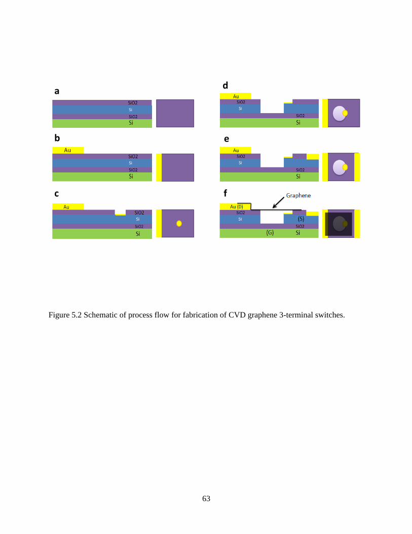
63
a
b
c
d
f
e
Figure 5.2 Schematic of process flow for fabrication of CVD graphene 3-terminal switches.

64
to define the source electrodes (Figure 5.2c). Then, larger circular wells (~5 µm diameter) are
etched overlapping each source electrode and through both the SiOx layer and the Si device layer
with a combination of buffered oxide etching (BOE 1:6) and RIE (Figure 5.2d-e). Finally, each
chip is separated into arrays of units by trenches (15 μm wide) etched down to the buried oxide
layer, and each unit is prepared for four potential devices. In each unit, two windows (200 μm x
80 μm) to the underneath source electrode are fabricated by RIE etching the top oxide layer and
depositing a layer of Cr/Au (5/60 nm). Graphene sheets are prepared by chemical vapor
deposition (CVD) on copper foil, and then patterned with oxygen plasma into arrays of 50 µm x
12 µm rectangular strips.[1]
Graphene sheets were transferred onto the substrates using a dry
transfer method.[2]
(Figure 5.2f)
Figure 5.3a and 5.3b is an optical image of a four unit array of graphene NEMS switches
and zoom in of a completed device, respectively. Atomic force microscope (AFM) images of
suspended graphene membranes were taken for more than 100 devices with a Veeco Dimension
3100 in non-contact mode (tip: µmasch, mode NSC15, 325 kHz, 46 N/m), and the majority of
initial deflections before electrical measurements at room temperature and atmosphere are
between 50-100 nm downward. (see Statistical distribution of the initial deflections in Section
5.10). This initial deflection was found to increase after electrical measurements were performed
suggesting that further slack is introduced in the graphene, presumably through sliding of the
graphene. Figure 5.3b is an example of the AFM image of the switch showing graphene
suspended over the etched well and electrically contacting the drain electrode. A side view
schematic of the completed device is shown in Figure 5.1. A monolayer graphene film is
electrically contacted to a drain electrode and suspended over a gate and source electrode (all of
which are electrically isolated from each other.)

65
DrainElectrode2 μm Suspended
Graphene
CVD Graphene10 μm
b
c
a
(d)
Source
Trench
Drain
200 µm
Figure 5.3 a) Optical image of a four unit array of graphene NEMS switches. b) Zoomed in
optical image of a single graphene NEMS switch located in the black rectangle in (a). c) Atomic
force microscope image of a graphene NEMS switch.

66
5.4 Electrical Measurement
The completed device can work either as a two-terminal or three-terminal NEMS switch.
All the electrical measurements are performed at 78 K and a pressure of ~10-6 Torr unless
otherwise indicated to eliminate the influence of capillary forces due to adsorbed water on device
operation. The low temperature electrical measurements in vacuum are measured in a Desert
cryogenic probe station cooled by liquid nitrogen. In 2-terminal operation, a voltage between the
source and drain electrodes, Vsd, is used to electrostatically deflect the graphene membrane.
When the graphene membrane gets sufficiently close to the source electrode it forms a
conducting pathway between the source and drain electrode which results in a current, Isd (Figure
5.4a). In 2-terminal operation the gate voltage is kept at Vg = 0. At a critical voltage of Vsd ~ 3.5
V, the current between the source and drain electrodes increases abruptly and the device switches
“on”; when Vsd is swept back to 0V the current abruptly decreases which leads to the “off”
position. The typical number of switching cycles measured is ~ 10-30. Figure 5.4b shows the
same device switching up to 30 times. There is some small scatter in the switching voltage but
most of the switching takes place between Vsd ~ 3.0 V– 3.5 V.
In 3-terminal operation, a constant Vsd is applied and then the gate voltage is swept until
switching commences. Data for a different graphene switch is shown in Figure 5.4c. The device
switches at Vg ~ 30 V, with Vsd = 4 V. Figure 5.4d shows the corresponding resistance, Rsd, vs Vg
for the same device. Initially the “off state” has a high resistance ~ 10 GΩ. As the gate voltage is
increased, there is an electrostatic force on the graphene membrane that pulls the graphene closer
to the drain electrode. This is supported by the resistance decreasing with Vg, suggesting some
tunnelling or leakage current between the graphene and drain electrode. At Vg
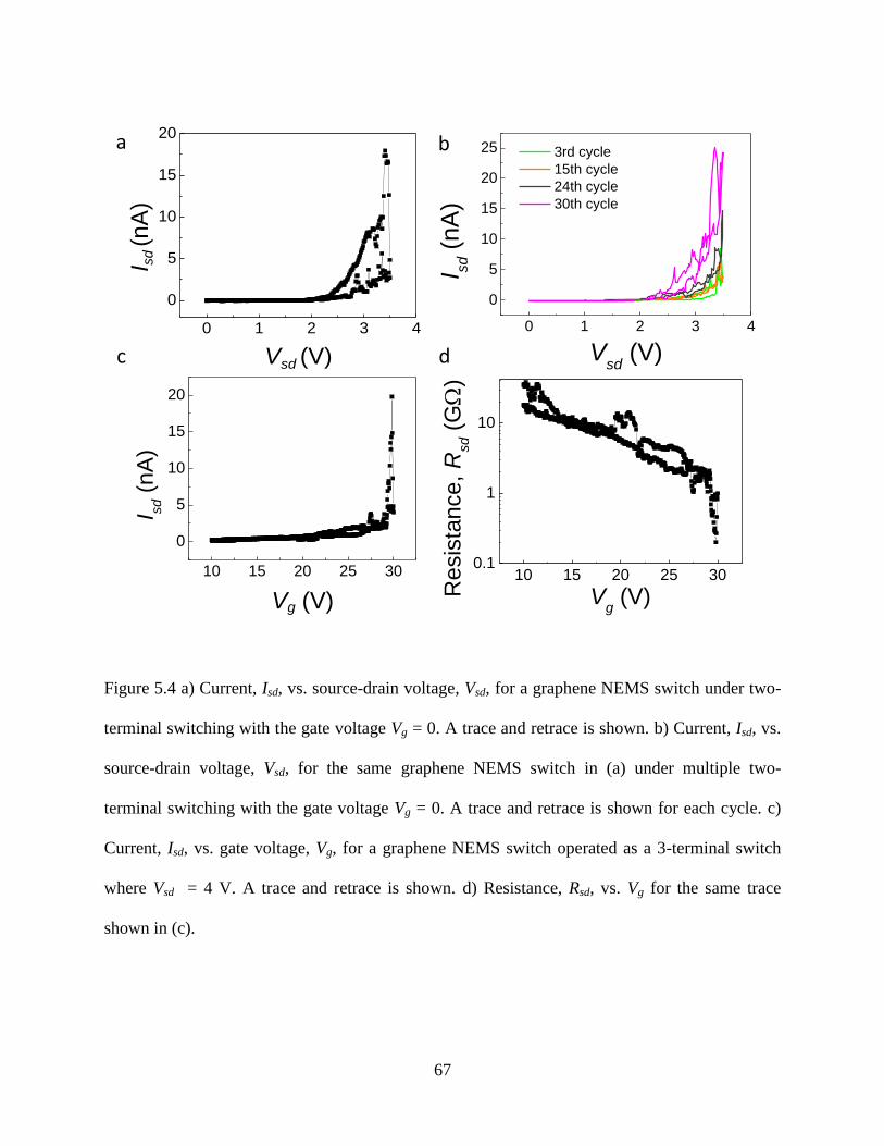
67
10 15 20 25 300.1
1
10
Re
sis
tan
ce
, R
sd (
G
)
Vg (V)
0 1 2 3 4
0
5
10
15
20
25 3rd cycle
15th cycle
24th cycle
30th cycle
I sd (
nA
)
Vsd
(V)0 1 2 3 4
0
5
10
15
20
I sd
(nA
)
Vsd (V)
a
10 15 20 25 30
0
5
10
15
20
I sd (
nA
)
Vg (V)
dc
b
Figure 5.4 a) Current, Isd, vs. source-drain voltage, Vsd, for a graphene NEMS switch under two-
terminal switching with the gate voltage Vg = 0. A trace and retrace is shown. b) Current, Isd, vs.
source-drain voltage, Vsd, for the same graphene NEMS switch in (a) under multiple two-
terminal switching with the gate voltage Vg = 0. A trace and retrace is shown for each cycle. c)
Current, Isd, vs. gate voltage, Vg, for a graphene NEMS switch operated as a 3-terminal switch
where Vsd = 4 V. A trace and retrace is shown. d) Resistance, Rsd, vs. Vg for the same trace
shown in (c).

68
~ 30 V, the graphene is sufficiently close to the drain electrode that more intimate contact is
made and the R decreases by ~ 1 order of magnitude. Both the 2-terminal and 3-terminal
switching I-V curves follow a similar behavior to other previously reported NEMS switches
where the current increases gradually at first following a smooth curve, and then increases
abruptly.[71,72,80,127]
For both the 2-terminal and 3-terminal switches, we define the voltage at the
point when the current starts to jump as the “threshold voltage”.
5.5 Verification of Electromechanical Switching
To rule out purely electrical effects in the switching behavior, we did some additional
experiments to distinguish the IV characteristics from graphene NEMS switches and graphene-Si
Schottky barriers, and then to verify that the measured electrical IV characteristics come from
the electromechanical actuated movements.
The electrostatic force that deflects the graphene membrane, Fe = - V2Aε0εr / 2d
2, is
symmetric with respect to the sign, where V is the applied voltage, A is the area of the membrane,
ε0 is the dielectric permittivity of vacuum space, εr is the dielectric constant, and d is the distance
between the graphene membrane and the underneath electrode. Therefore, switching should be
symmetric for positive and negative voltages, which is indeed the case. One example is shown in
Figure 5.5, with the optical image in Figure 5.5a . For two-terminal switching with positive and
negative Vsd, the threshold Vsd is ~ 6 V and ~ -6 V respectively (Figure 5.5b). Three terminal
switching from the same device demonstrates similar symmetry. When sweeping the gate
voltage in the positive range with Vsd = 4 V, the threshold Vg is ~ 28V (Figure 5.5c). For the
opposite case, the threshold Vg is ~ -28 V with Vsd = -4 V (Figure 5.5d). However, this kind of
symmetry is not observed in graphene-Si Schottky barriers.[131,132]

69
-6 -4 -2 0 2 4 6
-0.5
0.0
0.5
1.0
1.5
I sd (
nA
)
Vsd
(V)
a
0 10 20 30
0
5
10
I sd (
nA
)
Vg (V)
Vsd = 4V
-30 -20 -10 0-8
-6
-4
-2
0
2
4
I sd (
nA
)
Vg (V)
Vsd = -4V
c
0 2 4 6 8 10 12 14 16
-150
-100
-50
0
50
Before Measurements
After Measurements
Defle
ctio
n (
nm
)
X (m)
b
d
e f
Figure 5.5 a) Optical image of the graphene NEMS switch. b) 2-terminal IV characteristic with
positive and negative Vsd. c) 3-terminal IV characteristic with positive Vsd and Vg. d) 3-terminal
IV characteristic with negative Vsd and Vg. e) AFM images of the graphene membrane in the
device (in the black rectangle) before and after the electrical measurements shown in Figure 5.5
b, c,d. f) Cross cuts of the AFM images before and after electrical measurements across the
center of the graphene membrane.

70
In addition, we checked if the graphene membrane in the device from which we took the
data in Figure 5.5b, c, d is suspended with atomic force microscope (AFM) imaging before and
after these electrical measurements to rule out the possibility that the graphene membrane got
stuck to the electrodes before measurement. The AFM images of the suspended graphene
membrane in the device before and after the electrical measurements are shown in Figure 5.5e,
and the images are of the same color scale. We observed that the graphene membrane remained
free standing before and after the electrical measurements. From the crosscuts of the AFM
images in Figure 5.5f, we also found that the graphene membrane dipped in about 10 nm, most
likely due to slack introduced in the graphene from the transfer process. This phenomenon can be
considered as further evidence of the electromechanical switching in the device.
5.6 Temperature Dependence
We also studied the temperature dependence of the threshold switching voltages in the
graphene NEMS switches and compared it with that of “stuck” devices. Figure 5.6a shows the 2-
terminal switching IV curves at four different temperatures ranging from 100 K to 225 K. With
the increase of temperature, the threshold Vsd voltage decreases. The three terminal switching
shows a similar dependence (Figure 5.6b). With the temperature increase from 100 K to 175 K,
the switching Vg decrease from more than 42 V to ~18 V with Vsd = 3V. The apparent
temperature dependence can be attributed to an increase in the tension on suspended graphene
with decrease of temperature, which has been observed for both CVD and exfoliated suspended
graphene membranes.[8, 9]
In comparison, the IVsd traces for this device after being “stuck”, the
schematic of which is shown in Figure 5.6c, for temperatures from 150 K to 300 K showed very
limited temperature dependence in contrast to the data in Figure 5.6d.

71
0 1 2 3 4
0
2
4
6 T = 100 K
T = 125 K
T = 150 K
T = 225 K
I sd (
nA
)
Vsd
(V)0 10 20 30 40
0
1
2
3
4
5
T = 100 K
T = 125 K
T = 150 K
T = 175 K
I sd (
nA
)
Vg (V)
-0.5 0.0 0.5 1.0 1.5 2.0 2.5 3.0 3.5 4.0-20
0
20
40
60
80
100
120
140 T = 150 K
T = 200 K
T = 250 K
T = 300 K
I sd (
nA
)
Vsd
(V)
(S)
(D)
(G)
Graphene
a
dc
b
Figure 5.6 Temperature dependence measurement. a) Two-terminal switching at different
temperatures from 100 K to 225K. b) Three-terminal switching at different temperatures from
100 K to 175 K. c) Schematic of a switch with graphene stuck to the source electrode. d) IVsd
characteristic of the “stuck device”.
72
5.7 Statistics of Threshold Voltage
We measured the threshold Vsd in 51 2-terminal devices with the same geometry and
dimensions (radius of cavities a = 2.5 µm, radius of source electrodes b = 1 µm) but varied the
separation between graphene and source electrodes, d1 (Figure 5.7a and 5.7b). The average
threshold voltage Vsd and standard deviation are 5.45 ± 0.85 V for devices with d1 = 120 nm
(Figure 5.7a), and 6.23 ± 0.89 V for d1 = 160 nm (Figure 5.7b), respectively. This decrease in the
average threshold Vsd is consistent with the simple electrostatic model where decreasing d1 leads
to a decreasing threshold Vsd. The measured threshold Vsd is as low as 3.5 V, and all of them are
less than 10 V. These low voltages are much smaller than typical MEMS switches (30 - 50 V)
and comparable to CMOS logic and conventional dynamic random access memory (RAM)
technology.[83,123]
We also measured 9 3-terminal graphene switches, and the threshold Vg ranges
from 20 V to 45 V, while Vsd is set as 3 V (Figure 5.7c).
5.8 Modeling and Analysis
To understand the mechanics of the switches, we numerically model our device using
non-linear finite element simulations with the software package Abaqus. We use a decoupled
electro-mechanical model that approximates the electrostatic force at a point (x,y) on the
deformable electrode to be the same as that between two parallel plates and this approach gives
a reasonable approximate solution (Figure 5.8a).[133–135]
The electrostatic pressure from the gate
electrode Pg and source electrode Psd on the graphene membrane are defined as follows:

73
4 5 6 7 8 90
2
4
6
8
10
Threshold Vsd (V)
Counts
4 5 6 7 8 90
1
2
3
4
5
Counts
Threshold Vsd
(V)
20 25 30 35 40 450
1
2
3
4
Counts
Threshold Vg (V)
a b
c
Figure 5.7 a) A histogram showing the number of devices vs. their respective switching voltage
for 2-terminal graphene NEMS switches with d1 = 120nm. The average and standard deviation
threshold Vsd = 5.45 ± 0.85 V. b) A histogram showing the number of devices vs. their
respective switching voltage for 2-terminal graphene NEMS switches with d1 = 160 nm. The
average and standard deviation threshold Vsd = 6.23 ± 0.89 V. c)A histogram showing the
number of devices vs. their respective switching voltage for 3-terminal graphene NEMS switches
with d1 = 120 nm and Vsd = 3 V.

74
( ( )) (5.1)
( ( )) (5.2)
here, d2 , d3 are the initial separations between source and box oxide layer, and the thickness of
the box oxide layer, ε0 is the dielectric permittivity of vacuum space, κ (= 3.9) is dielectric
constant of silicon dioxide,[136]
while w(x,y) gives the deflection of the graphene membrane as
function of the x and y coordinates. The electrostatic pressure Pg and Psd act on regions of the
graphene directly above the gate and drain electrodes respectively.
The schematic of the switch is as shown in Figure 5.8b. The switch can operate either in
2-terminal or 3-terminal configurations, the difference being that in the 2-terminal operation Vg is
set to zero. The simplified finite element (FE) model is also shown in Figure 5.8c. The
suspended graphene membrane (drain) is the deformable electrode while the source and gate are
rigid and fixed. Hence only the deformable part of the graphene membrane is actually part of the
FE model while the rest of the switch is modeled through constraints and loads. The graphene
membrane is fixed along the edges and advantage is taken of the two fold symmetry by applying
a symmetry boundary condition. The electrostatic forces due to the electric fields between the
drain and source electrodes as well as the drain and gate electrodes that deform the graphene
membrane are described by equations (1) and (2) in the main text. These position dependent
loads have been applied using DLOAD sub-routine of Abaqus.[3]
The graphene membrane is
modeled with S4R (4 noded shell elements with reduced integration) elements to include both
bending and stretching effects.[137,138]
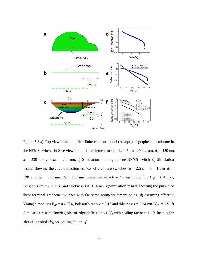
75
c
2b
d1
Source
2a
Graphene
Gate
EdgeDeflection
d2 + d3/k
MaxDeflection
b
a
0 5 10 15 20 25-160
-120
-80
-40
0
Max Deflection
Edge Deflection
Defle
ctio
n (
nm
)
Vg (V)
0 2 4 6-120
-90
-60
-30
0
Ed
ge
Defle
ctio
n (
nm
)
Vsd (V)
0 5 10 15 20 25 30
-120
-100
-80
-60
-40
-20
0
0 2 4 6 8 10
10
15
20
25
Thre
shold
Vg (
V)
Scaling Factor, sf
scaling facctor = 1
scaling facctor = 2
scaling facctor = 4
scaling facctor = 6
scaling facctor = 8
scaling facctor = 10
Ed
ge
De
fle
ctio
n (
nm
)
Vg (V)
f
e
d
Figure 5.8 a) Top view of a simplified finite element model (Abaqus) of graphene membrane in
the NEMS switch. b) Side view of the finite element model. 2a = 5 µm, 2b = 2 µm, d1 = 120 nm,
d2 = 230 nm, and d3 = 200 nm. c) Simulation of the graphene NEMS switch. d) Simulation
results showing the edge deflection vs. Vsd of graphene switches (a = 2.5 µm, b = 1 µm, d1 =
120 nm, d2 = 230 nm, d3 = 200 nm), assuming effective Young’s modulus Eeff = 0.4 TPa,
Poisson’s ratio ν = 0.16 and thickness t = 0.34 nm. e)Simulation results showing the pull-in of
three terminal graphene switches with the same geometry dimension as (d) assuming effective
Young’s modulus Eeff = 0.4 TPa, Poisson’s ratio ν = 0.16 and thickness t = 0.34 nm. Vsd = 3 V. f)
Simulation results showing plot of edge deflection vs. Vg with scaling factor = 1-10. Inset is the
plot of threshold Vsd vs. scaling factor, sf.

76
As the electrostatic load is increased, the membrane deforms and comes closer to the
electrodes and at the threshold voltage, pulls-in, thereby making contact and completing the
circuit. This contact occurs along the axis of symmetry at the edge of the post (source electrode).
We call the deflection of the membrane at this point the “edge deflection”. In the two-terminal
operation, the pull-in is caused solely by Vsd while in the three-terminal operation it is caused by
increasing Vg. The results show that the pull-in in the three-terminal case is a local phenomenon
as the maximum deflection that occurs near the center of the suspended region along the axis of
symmetry shows no abrupt change with increasing Vg.
An example of the simulation results for 2-terminal and 3-terminal configurations are
shown in Figure 5.8d and 5.8e respectively assuming the effective Young’s modulus of CVD
graphene Eeff = 0.4 TPa, which is about 40% of the Young’s modulus of exfoliated monolayer
graphene but is reasonably close to a recently reported value for CVD graphene.[139]
The
geometrical dimensions are: a = 2.5 µm, b = 1 µm, d1 = 120 nm, d2 = 230 nm and d3 = 200 nm.
In the finite element simulations of 2-terminal switching, Vsd is varied continuously until the
membrane is pulled-in,[69,140]
which is shown by an abrupt drop in the deflection of graphene
membrane above the edge of source electrode as defined in Figure 5.8c. For the simulation of 3-
terminal operation of devices with the same dimensions, Vsd is fixed at 3 V and Vg is varied until
the graphene membrane is pulled into contact with the source electrode. The threshold Vsd and
Vg obtained from the simulations are 5.3 V and 23.4 V, respectively. Using the finite element
simulations, we took Eeff to be a fitting parameter and derived a distribution of Eeff from the data
shown in Figure 5.7. To fit the data in Figure 5.7a and 5.7c, an average value of Eeff = 0.4 TPa is
required, while an average of Eeff = 0.15 TPa for the data in Figure 5.7b. We think the scatter
and deviation in the data of threshold voltages are caused by wrinkles or slack, both initial slack

77
in the transferred graphene and slack introduced through sliding caused by the electrostatic
actuation; furthermore, the range of Eeff is in line with reported values from CVD graphene.[139]
Further detailed studies of the deformation mechanisms would be needed to conclusively resolve
these uncertainties, but the overall behaviour appears to be adequately described by the model
with the modulus adjusted to account for various potential softening mechanisms.[139]
5.9 Size Scaling
The threshold voltages for our 3-terminal switches range from 20 V to 45 V. However,
we find that the value decreases by further scaling down the dimension of the devices in a study
of scaling effects with finite element simulations similar to previous ones. We scaled down all
the dimensions (initial dimensions: a = 2.5 µm, b = 1 µm, d1 = 120 nm, d2 = 230 nm, d3 = 200
nm) by the same scaling factor (sf) and did the simulations in the 3-terminal configuration. The
results of these simulations, where the deformations scaled exactly with the inverse of the scaling
factor, are shown through gate voltage (Vg) versus edge deflection plots in Figure 5d. The
simulated threshold Vg decreased with sf increasing from 1 to 10. When the device is scaled
down by 10 times (final dimensions with sf = 10: a = 250 nm, b = 100 nm, d1 = 12 nm, d2 = 23
nm, d3 = 20 nm), the threshold Vg is found to be decreased to 7.4 V from 23.5 V with Vsd = 3 V,
shown in the inset of Figure 5.8f. This indicates that we can potentially have larger device
densities with lower actuation voltages and improved efficiencies just by scaling down the
devices.

78
a b
-175 -150 -125 -100 -75 -50 -25 00
2
4
6
8
10
12
14
16
Co
un
ts
Deflection (nm)
Before Switching
After Switching
-35 -30 -25 -20 -15 -10 -5 00
5
10
15
Co
un
tsDeflection Change (nm)
Figure 5.9 a) Statistical distribution of center deflections measured by AFM of graphene
membranes from one chip before and after ~10 times electrical switching. b) Statistical
distribution of the change of center deflection after the electrical measurements.

79
5.10 Sliding during Switching
We took AFM images before and after the electrical measurements of more than 100
suspended graphene membrane devices. The statistical distribution of the center deflections of
the graphene membranes from 49 devices on one chip before and after 1-10 times of
electromechanical switching is shown in Figure 5.9a. The majority of the center deflections
before and after electrical measurements are 50-100 nm downward, while the depth of the
underneath source electrodes is ~200 nm. After electromechanical switching, most of the
graphene membranes have a larger initial deflection, and the deflection changes are plotted in
Figure 5.9b. These changes range from 0 nm to 35 nm with the majority being within 10 nm.
5.11 Graphene 3-Terminal Switches with a Different Geometry
We developed a different geometry for the graphene NEMS switches. The side view schematic
and top view of the switch is shown in Figure 5.10a. Instead of a Au coated circular source
electrode at the edge of the predefined well on which graphene membrane is suspended, a
uniform step around the edge of the well is etched with BOE 1:6 and the exposed heavily doped
device Si layer is exposed as the source electrode. The width of the step is 0.3 – 1 μm, and the
depth of the step (d1) above the source electrodes ranges from 100 nm to 220 nm as well. An
example of switching IV characteristics of a graphene NEMS switch is shown in Figure 5.10b
and 5.10c. The threshold Vsd and Vg are 7 V and 34.5 V, respectively. Figure 5.10d shows a
switching IV curve for a three-terminal switch at room temperature. The threshold Vg is ~12V
with Vsd = 2.8 V, close to the requirement for CMOS IC integration.[83]
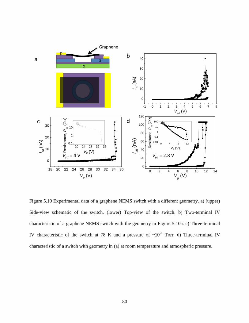
80
18 20 22 24 26 28 30 32 34 36
0
10
20
30
I sd (
nA
)
Vg (V)
20 24 28 32 360.1
1
10
Re
sis
tan
ce
, R
sd (
G
)
Vg (V)
-1 0 1 2 3 4 5 6 7 8
0
10
20
30
40
I sd (
nA
)
Vsd
(V)
a
c
D
G
S
Vsd = 4 V
0 2 4 6 8 10 12 14
0
20
40
60
80
100
120
I sd (
nA
)
Vg (V)
0 4 8 120.01
0.1
1
10
100
Resi
stan
ce,
Rsd
(G
)Vg (V)
d
b
Graphene
Vsd = 2.8 V
Figure 5.10 Experimental data of a graphene NEMS switch with a different geometry. a) (upper)
Side-view schematic of the switch. (lower) Top-view of the switch. b) Two-terminal IV
characteristic of a graphene NEMS switch with the geometry in Figure 5.10a. c) Three-terminal
IV characteristic of the switch at 78 K and a pressure of ~10-6
Torr. d) Three-terminal IV
characteristic of a switch with geometry in (a) at room temperature and atmospheric pressure.
81
5.12 Conclusion
In conclusion, we fabricated and characterized a large array of graphene NEMS switches
with a unique design, with which sub – 5 V actuation and an improved mechanical integrity of
the graphene membrane is achieved. This design, with the graphene membrane having a “line”
contact during switching, holds the promise to address the adhesion challenges in graphene
nanomechanical switches. We also study the effect of scaling to the decrease of actuation voltage
with simulation, thereby providing an instructive guide for further scaling of graphene NEMS
switches.
82
Chapter 6
Measurement of Interfacial Forces in
Graphene Membranes
6.1 Introduction
Interfacial forces act between all materials[64]
. At macroscopic distances, these interfacial
forces are weak and practically insignificant, but at distances approaching tens of nanometers,
they become much stronger, thereby enhancing the attraction within micro/nanomechanical
structures or molecules, and potentially significantly affecting the device performance[88,95,96,141]
.
Graphene, a 2 dimensional nanomaterial composed of carbon atoms, is a promising material with
potential applications in a variety of nanomechanical, biological and electrical devices due to its
exceptional properties[7,18,22,25,32,141–143]
. Furthermore, graphene being extremely thin with a very
high surface area to volume ratio is highly susceptible to interfacial forces and is an ideal
candidate to study and characterize these forces.[103,144]
Therefore, there is an increasing interest
in studying the nature of interfacial forces on graphene.[58]
Even though the adhesion strength
between graphene and substrates when in contact has been experimentally measured in different
ways, experimental measurements of non-contact attractive interfacial forces remains relatively
unexplored.[56,57,102,145]
Interfacial forces on bulk materials or other nanomaterials have been
measured using a variety of configurations.[64,88,141,146]
Here, we demonstrate a novel
experimental method to study these elusive forces on graphene with a real time observation of
the induced pull in instability.
83
6.2 Fabrication
Devices used in this study consist of a graphene flake suspended over an annular ring
etched into a silicon oxide wafer, forming a graphene-sealed microcavity (Figure 6.1a). Device
configurations include graphene suspended on bare SiOx or gold-coated SiOx. Suspended
graphene membranes were fabricated by a combination of standard photolithography, reactive
ion etching and mechanical exfoliation of graphene. An array of annular cavities with designed
dimensions was first defined by photolithography on an oxidized silicon wafer with a silicon
oxide thickness of 90/285 nm. Reactive ion etching was then used to etch the annular rings into
microcavities with a depth of 100-120 nm. After removal of photoresist with acetone and
isopropanol, the chips were further cleaned in a Nanostrip bath at 60°C for 20 minutes. Thermal
evaporation is used to deposit a layer of Cr/Au 5/10 nm for the Au coated annular rings. During
the evaporation process, the chips are tilted at a 10~15° angle, so that the Cr/Au atoms can be
deposited into the annular rings and cover the side walls. The large aspect ratio between the
width and depth of the annular ring allows for a conformal metal deposition such that the post
and the substrate are electrically contacted and grounded. Mechanical exfoliation of natural
graphite using Scotch tape was then used to deposit suspended graphene sheets over the
microcavities.
6.3 Observation of Pull-in Instability
The graphene membranes are pressurized using a previously-developed technique.[32,56]
The suspended graphene membranes are placed in a high pressure chamber at a charging
pressure, pext ~ 300 kPa of H2 gas, and left for a sufficiently long time (~10 hours) until the
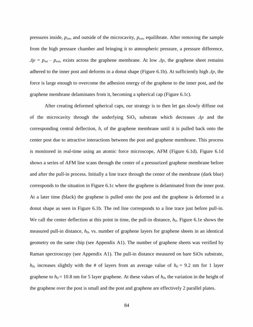
84
pressures inside, pint, and outside of the microcavity, pext, equilibrate. After removing the sample
from the high pressure chamber and bringing it to atmospheric pressure, a pressure difference,
Δp = pint – pext, exists across the graphene membrane. At low Δp, the graphene sheet remains
adhered to the inner post and deforms in a donut shape (Figure 6.1b). At sufficiently high Δp, the
force is large enough to overcome the adhesion energy of the graphene to the inner post, and the
graphene membrane delaminates from it, becoming a spherical cap (Figure 6.1c).
After creating deformed spherical caps, our strategy is to then let gas slowly diffuse out
of the microcavity through the underlying SiOx substrate which decreases Δp and the
corresponding central deflection, h, of the graphene membrane until it is pulled back onto the
center post due to attractive interactions between the post and graphene membrane. This process
is monitored in real-time using an atomic force microscope, AFM (Figure 6.1d). Figure 6.1d
shows a series of AFM line scans through the center of a pressurized graphene membrane before
and after the pull-in process. Initially a line trace through the center of the membrane (dark blue)
corresponds to the situation in Figure 6.1c where the graphene is delaminated from the inner post.
At a later time (black) the graphene is pulled onto the post and the graphene is deformed in a
donut shape as seen in Figure 6.1b. The red line corresponds to a line trace just before pull-in.
We call the center deflection at this point in time, the pull-in distance, h0. Figure 6.1e shows the
measured pull-in distance, h0, vs. number of graphene layers for graphene sheets in an identical
geometry on the same chip (see Appendix A1). The number of graphene sheets was verified by
Raman spectroscopy (see Appendix A1). The pull-in distance measured on bare SiOx substrate,
h0, increases slightly with the # of layers from an average value of h0 = 9.2 nm for 1 layer
graphene to h0 = 10.8 nm for 5 layer graphene. At these values of h0, the variation in the height of
the graphene over the post is small and the post and graphene are effectively 2 parallel plates.

85
0.0 0.5 1.0 1.5 2.0 2.5 3.0
0
5
10
15
20
25
30
35
40
Deflection (
nm
)
X (m)
a b c
d e
2b
2a
pint
pext Δp = pint - pext
h0
1 2 3 4 58.5
9.0
9.5
10.0
10.5
11.0
11.5
Pull
in d
ista
nce
, h
0 (
nm
)
# of layers
Figure 6.1 a) (upper) Optical image of suspended a few layer graphene membrane in an annular
ring geometry. (lower) Side view schematic of the suspended graphene on the annular ring. b)
(upper) A 3d rendering of an AFM image of a pressurized graphene membrane in the annular
ring geometry before delamination from the inner post. (lower) Side view schematic of the
pressurized suspended graphene on the annular ring. c) (upper) A 3d rendering of an AFM image
of a pressurized graphene membrane in the annular ring geometry after delamination from the
inner post. (lower) Side view schematic of the pressurized suspended graphene delaminated from
the inner post. d) A series of AFM line cuts through the center of a pressurized graphene
membrane during pull in. The outer diameter, 2a = 3 µm, and inner diameter, 2b = 0.5 µm. e)
Pull in distance, h0, vs. number of layers for graphene membranes in an annular ring geometry
with 2a = 3 µm and 2b = 0.5 µm. (upper left inset) Side view schematic of the graphene
membrane right before and after pull in.
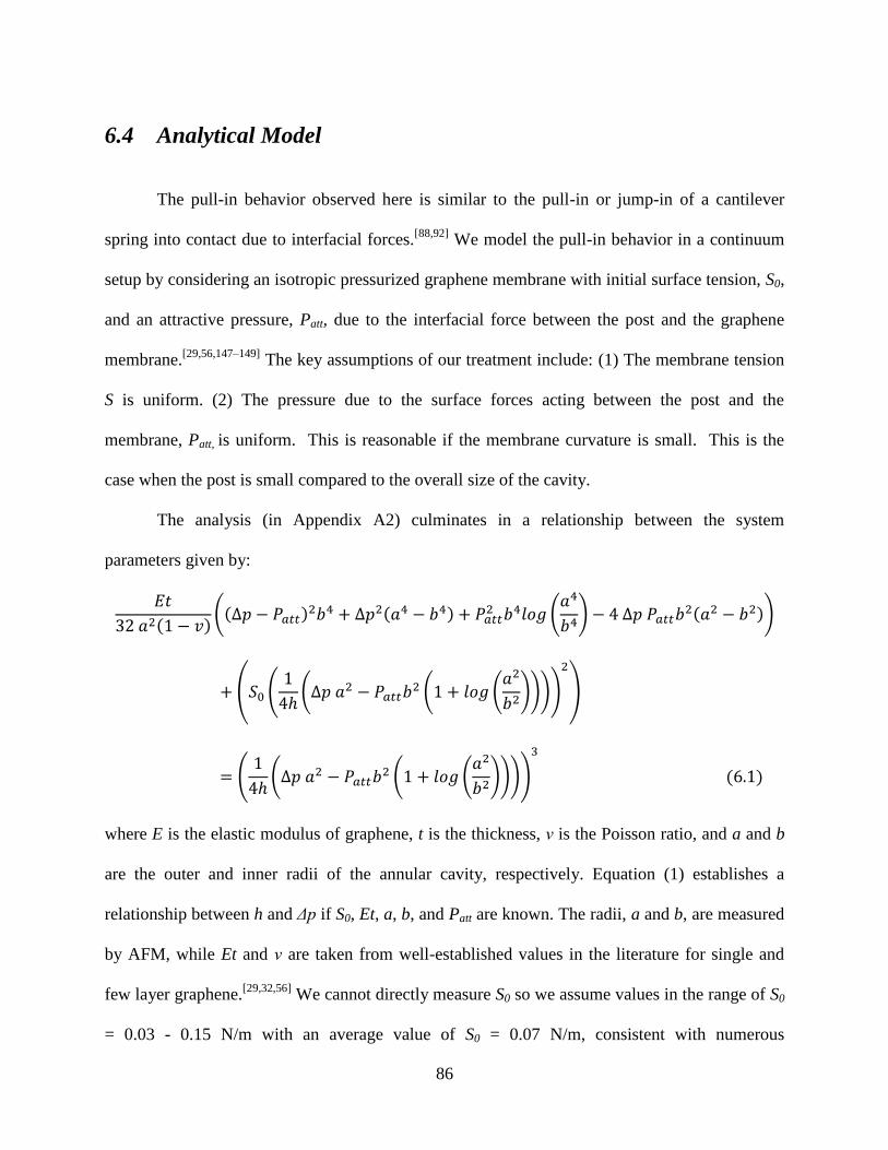
86
6.4 Analytical Model
The pull-in behavior observed here is similar to the pull-in or jump-in of a cantilever
spring into contact due to interfacial forces.[88,92]
We model the pull-in behavior in a continuum
setup by considering an isotropic pressurized graphene membrane with initial surface tension, S0,
and an attractive pressure, Patt, due to the interfacial force between the post and the graphene
membrane.[29,56,147–149]
The key assumptions of our treatment include: (1) The membrane tension
S is uniform. (2) The pressure due to the surface forces acting between the post and the
membrane, Patt, is uniform. This is reasonable if the membrane curvature is small. This is the
case when the post is small compared to the overall size of the cavity.
The analysis (in Appendix A2) culminates in a relationship between the system
parameters given by:
( )(( )
( ) (
)
( ))
( (
(
( (
))))
)
(
(
( (
))))
( )
where E is the elastic modulus of graphene, t is the thickness, ν is the Poisson ratio, and a and b
are the outer and inner radii of the annular cavity, respectively. Equation (1) establishes a
relationship between h and Δp if S0, Et, a, b, and Patt are known. The radii, a and b, are measured
by AFM, while Et and ν are taken from well-established values in the literature for single and
few layer graphene.[29,32,56]
We cannot directly measure S0 so we assume values in the range of S0
= 0.03 - 0.15 N/m with an average value of S0 = 0.07 N/m, consistent with numerous

87
experimental measurements for exfoliated suspended graphene membranes in a similar
geometry.[32,150,151]
Figure 6.2a shows the relationship between h vs. Δp obtained from equation
(1) using the system parameters for a monolayer graphene membrane: a = 1.5 µm, b = 0.25 µm,
S0 = 0.07 N/m, Et = 340 N-m, ν = 0.16, and Patt = β/h4 = 0.0199 nN-nm
2/h
4. The deflection, h
decreases with decreasing Δp (leaking gas) until a critical point is reached. At this critical
maximum deflection, h0, the graphene is sufficiently close to the post and pulled into the post by
the attractive force. This pull-in instability is illustrated by the point on the curve where the slope
goes to infinity at the pull in distance h0, or:
|
(6.2)
The measured h0, a, and b, coupled with the values of S0, Et, and ν taken from the literature,
allow us to determine Patt by solving eqs. (1) and (2) simultaneously for Δp and Patt.
6.5 Finite Element Analysis
To validate the analytical model, we also carried out high-fidelity finite element
simulations of the experimental configuration using the code Abaqus where we remove the
assumptions used to develop the analytical model. The model used in the simulations is shown in
Figure 6.2. Axisymmetric shell elements (that permit both bending and membrane behaviour)
were used and the Young’s modulus and Poisson’s ratio were set to 1 TPa[29]
and 0.16[152]
respectively. The outer edge of the membrane is pinned and the substrate/post is modelled as a
fixed analytical rigid body. Since it is known that pressurized graphene behaves like a membrane
and bending plays a negligible role in its mechanics[56,145]
, the value of the bending modulus and

88
a
b
Figure 6.2 Schematic of the model. a) Schematics showing the equilibrium condition for the two
regions of the membrane. b) Schematic of the model used for finite element analysis simulations.

89
slope near the boundary is found to be irrelevant in these simulations. A prescribed initial tension
is applied and the attractive interactions between the substrate and the membrane are modelled as
surface-to-surface contact/adhesive interactions with the substrate being the master surface. The
contact interaction properties are supplied through the user subroutine “UINTER” of Abaqus.
The slave nodes experience a tensile (attractive) contact stress ( ) only in the vertical direction
given by,
( )
( ) (6.3)
Here, is a parameter and is the deflection of the node measured from the substrate. Both
and w are functions of the radial position, in contrast to the analytical model where they are
assumed to be independent of position.
The simulation is split into two steps – both static steps with nonlinear geometric effects
included. In the step 1, the contact/adhesive interactions are suppressed and the membrane is
allowed to deform under the influence of a uniform pressure load acting on the entire area of the
suspended membrane. The magnitude of this load is set such that the deflection is just high
enough to neglect the interaction pressure if the interactions were not suppressed. This simulates
the state of affairs at the beginning of the experiment before the gas begins to leak from the
cavity. In the second step, which is a Static-Riks step, a second uniform pressure load is added
with the same magnitude as the previous pressure load but in the opposite direction and the
surface interactions between the substrate and the membrane are switched on. Hence at a given
increment during the step, apart from the force due to the contact interactions, the membrane has
the uniform pressure load from the previous step and a uniform pressure in the opposite direction
whose value is given by the load proportionality factor. The superposition of these two uniform

90
ba
c d
Figure 6.3 a) Plots comparing p vs h behavior as obtained from the FE simulations (solid curve)
and the analytical calculations (dashed curve) with a = 1.5 , b = 0.25 , Et = 340 N/m, =
0.16, S0 = 0.07 N/m and = 0.02 nN-nm2. b) The deflection profiles at different pressures (solid
– FE, dashed – Analytical) (Red – 10.38 kPa, Blue – 6.12 kPa, Green – 1.72 kPa and Magenta –
2.61 kPa). For convenience, the corresponding points on p vs h plot are also shown. (c) and (d)
The same as (a) and (b) except b = 0.75 . The different pressures used in this case are: Red –
10.39 kPa, Blue – 6.14 kPa, Green – 2.63 kPa and Magenta – 3.70 kPa.

91
pressure loads mimics the leaking of the gas in the experiment. As the simulation progresses, the
load across the membrane decreases and it comes closer to the substrate. This increases the
interaction between the post and membrane. The results of this step are plotted in Figure 6.2a of
the main text. It can be seen that the load across the membrane initially decreases until a limit
point is reached and then it starts increasing. The limit point gives the pull-in distance and the
pressure at which it occurs. The configurations below the limit point can’t be achieved in a load
controlled experiment, but suggest that system has two possible equilibrium configurations at a
given pressure load greater than the pull-in pressure. Careful comparison of the analytical and
finite element simulation results (Figure 6.3) shows that the analytical result is an accurate
description of the physical phenomena as long as the substrate/post size is small compared to the
size of the suspended membrane.
A comparison to a high-fidelity finite element model that more accurately treats the
spatial dependence of the attractive forces is shown in blue on Figure 6.4a; the close agreement
between them supports the validity of our analytical model.
6.6 Layer Dependence
We assumed an attractive force law of the form Patt = β/h4, consistent with the van der
Waals (vdW) force derived from Lifshitz theory between graphene and SiO2 for separations on
the order of 10 nm or the phenomenological Lennard-Jones pair potential of interaction.
[64,65,90,153,154]From the experimentally measured pull-in distances in Figure 6.1e we calculate β
for each device and arrive at the corresponding Patt(h = h0) . This is shown in Figure 6.4b where
β = 0.0199 nN-nm2 for monolayer graphene. This value is ~1.5% of the dispersion force between
2 perfectly metallic parallel plates, Patt = πћc/240h4 = 1.3 nN-nm
2/h
4,[90]
and agrees reasonably
92
1 2 3 4 5
0.02
0.04
0.06
0.08
0.10
(
nN
-nm
2)
# of layers
0 2 4 6 8 100
5
10
15
20
25
30
35
Cen
ter
defle
ctio
n,
h (
nm
)
p (kPa)
leaking
a b
h0
Figure 6.4 Scaling of β with Number of Layers. a) Center deflection, h, vs. pressure difference,
Δp, calculated for a monolayer graphene membrane in the annular ring geometry with an outer
diameter, 2a = 3 µm, and inner diameter, 2b = 0.5 µm. The red dashed line at Δp = 1.68 kPa
corresponds to pull-in and the deflection at this point is h0 = 9.2 nm. The black line corresponds
to the analytical model and the blue line is a finite element analysis model. b)The calculated
values of β vs. number of layers using the data in (a) assuming a model where the force
responsible for pull-in has the form Patt = β/h4. The initial tension S0 is assumed to be 0.07 N/m.
A best fit line through the data is also shown which has a slope of 0.017 nN-nm2/# of layer.

93
well with recent theoretical calculations for graphene and SiO2 at 10 nm separations, β = 0.001
nN-nm2 - 0.01 nN-nm
2for an intrinsic graphene doping density of 10
14 m
-2 and 10
16 m
-2 at T =
300 K, respectively.[153]
Figure 2b also shows that β increases linearly with # of layers, up to 5
layers, with a slope of 0.017 nN-nm2/layer, close to the measured value of monolayer graphene,
β = 0.0199 nN-nm2. This increase with layer number suggests that the strength of the force is
increasing in an integer manner as additional graphene layers are added. This is consistent with
the additive nature of the vdW force.[64,153]
Our results are interesting in the context of recent
experiments where an AFM tip was pulled off of a graphene substrate where the pull-off force
was observed to depend on the number of graphene layers in suspended membranes,[155]
but not
on graphene supported by a substrate.[155,156]
Despite this similarity in response, we note that
pull-off experiments are well-known to be different mechanistically than the pull-in experiments
of our study.
6.7 Power Law Study
In addition to vdW force, the interfacial forces can be from capillary or electrostatic
forces. The capillary forces take effect when graphene membranes or the substrate are covered
with liquid films and the liquid films touch, and the force can be described by Patt 1/h.[64,154,157]
However, we assume that the capillary force is not a likely candidate for the interfacial forces
causing the pull-in phenomenon because absorbed liquid films of 10 nm thickness are unlikely to
form between graphene membranes and the substrate.[158,159]
The electrostatic interaction, which
can arise from image charges, work function differences or patch potentials can be described by
Patt 1/h2.[64,160,161]
To further study the power law model considering different origins of the
interaction, we varied the geometry of the annular ring. The pull-in distance for 1-4 layers

94
0 500 1000 1500 2000 2500
6
8
10
12
14
16
18
20
22
Pull
in d
ista
nce,
h0 (
nm
)
Inner diameter, 2b (nm)
0 200 400 600 800 10002
4
6
8
10
12
14
16
Pull
in d
ista
nce
, h
0 (
nm
)
Inner diameter, 2b (nm)
200 400 600 8006
8
10
12
14
16
Pull
in d
ista
nce
, h
0 (
nm
)
Inner diameter, 2b (nm)
200 400 600 800
8
10
12
14
16
Pull
in d
ista
nce
, h
0 (
nm
)
Inner diameter, 2b (nm)
1 layer 2 layers
3 layers 4 layers
a b
c d
Figure 6.5 Scaling of the Pull in Distance with Patt. Pull in distance, h0, vs. inner diameter, 2b,
for a) 1 layer b) 2 layer c) 3 layer d) 4 layer graphene flakes (verified by Raman spectroscopy)
with identical outer diameter but different inner diameters. The black and blue shaded lines are
the calculated results for 2 different power law dependences Patt = β/h4 (black) and Patt = α/h
2
(blue) with S0 = 0.03 – 0.09 N/m. The values of β and α are listed in supplementary material. a)
(inset) Optical image of 2 of the measured monolayer devices. The scale bar = 5 µm.

95
graphene membranes with an identical outer diameter but a different inner diameter is shown in
Figure 6.5. The pull in distance shows a slight increase with increasing b. A theoretical
calculation based on our analytical model using Patt = β/h4 and the calculated values of β in
Figure 6.2b, is shown as a black shaded line in Figure 6.3. The boundaries of the shaded lines
show the range of values for S0 = 0.03 – 0.09 N/m.[151]
To determine if electrostatic forces play a significant role in our measurements, we fit the
data in Figure 6.1e and Figure 6.3 with a model in which an electrostatic force takes the form,
Patt = α/h2, and we use the same strategy to determine α as was used to calculate β above. Doing
so for the monolayer devices in Figure 1e, gives α = 0.49 pN (for S0 = 0.07 N/m). We can also
use these values of α to fit the data in Figure 6.3. This is shown as a shaded blue line which fits
poorly to the data. A good fit would require that α increase with inner post diameter for all the
devices measured, while no such assumption is needed for β. To fit all of our measured pull-in
distances (51 devices in 17 geometries from 5 different chips) using an electrostatic force model
requires that α values vary from 0.15 – 1.79 pN across all the devices. A model based on an
inverse 3rd
power dependence was also examined and does not fit all the data as well as the
inverse fourth power dependence (see Appendix A3).
6.8 Materials Dependence
To test the material dependence of the interfacial interaction with graphene, we also
carried out experiments where we measured the pull-in distance between graphene and a gold
coated annular ring that were electrically contacted and grounded. 2-5 layers graphene
membranes (17 devices in 6 similar geometries from 4 chips) were measured. The pull in
distance varied between 9 nm and 18 nm for annular rings with

96
0 5 10 15 20 25 30 35 40 45 50 551E-3
0.01
0.1
1
10
la
yer(n
N-n
m2)
Counts
Figure 6.6 Modelled vdW force vs. Number of Layers for SiOx and Gold. Measured β / Number
of graphene layers between SiOx and 1 layer graphene (solid red squares), 2 layer graphene
(solid green circles), 3 layer graphene (solid blue up triangles), 4 layer graphene (solid cyan
down triangles), 5 layer graphene (solid magenta diamond), and β / number of graphene layers
between Au and 2 layer graphene (hollow green circles), 3 layer graphene (hollow blue up
triangles), 4 layer graphene (hollow cyan down triangles), and 5 layer graphene (hollow magenta
diamond). The average and standard deviation of β / Number of graphene layers between SiOx
and graphene are 0.0179 0.0037 nN-nm2 / layer. The average and standard deviation of β /
Number of graphene layers between Au and graphene are 0.104 0.031 nN-nm2 / layer. Each
data point corresponds to a separate device. (top left inset) Side view schematic of the
pressurized suspended graphene on the annular ring with SiOx surface. (top right inset) Side view
schematic of the pressurized suspended graphene on an Au coated annular ring.

97
a = 1-1.75 µm and b = 0.15-0.6 µm, slightly larger than the measured pull-in distances for
uncoated SiOx posts of a similar geometry. Using the same theoretical analysis as with the
graphene/SiOx data, we determined the average value and standard deviation of β / # of graphene
layers between the Au coated post and electrically grounded graphene to be = 0.104 0.031 nN-
nm2 / layer; these are about an order of magnitude higher than those for graphene interacting
with SiOx (Figure 6.6). The graphene/Au values agrees reasonably well with the theoretical
predictions based on a Lifshitz formula of graphene interacting with gold at 15 nm separation, β
= 0.08 nN-nm.
6.9 Deformation of Graphene Membranes by vdW Force
The extreme flexibility of the suspended graphene coupled with the large magnitude of
the interfacial force at these short separations shows up as a statically deformed membrane right
before pull-in for some devices. This is especially evident for a graphene membrane with a small
inner post – more localized force- and a large outer diameter – more flexible graphene (Figure
6.5). The AFM image shows a graphene membrane locally deformed at its center shortly before
pull-in (Figure 6.7a). The AFM line cut through the center (Figure 6.7b) shows this deformation
to be about 2 nm. This deformation is further verified by the analytical model which shows a
number of stable configurations for graphene membranes deformed by Patt at these dimensions
and separations (Figure 6.7c).
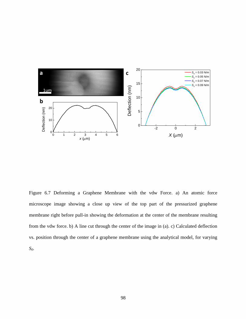
98
0 1 2 3 4 5 60
10
20
De
fle
ctio
n (
nm
)
x (m)
1um
a
b
-2 0 20
5
10
15
20 S
0 = 0.03 N/m
S0 = 0.05 N/m
S0 = 0.07 N/m
S0 = 0.09 N/m
Defle
ctio
n (
nm
)
X (m)
c
Figure 6.7 Deforming a Graphene Membrane with the vdw Force. a) An atomic force
microscope image showing a close up view of the top part of the pressurized graphene
membrane right before pull-in showing the deformation at the center of the membrane resulting
from the vdw force. b) A line cut through the center of the image in (a). c) Calculated deflection
vs. position through the center of a graphene membrane using the analytical model, for varying
S0.

99
6.10 Conclusion
In conclusion, we observed the pull in instability at 10nm-20nm distance on graphene by
the attractive interfacial forces between graphene and SiOx/Au, and found them to agree very
well with a form Patt = β/h4, consistent with recently calculated values of long range vdW forces
between graphene and SiOx and graphene and gold. Furthermore, the strength of the force scales
linearly with layer numbers, which is compatible with the additive nature of vdW forces. It is
noteworthy that our experimental configuration is essentially a realization of a parallel plate
geometry by self-alignment to measure interfacial forces acting on atomically thin, two-
dimensional materials41
. These experiments which provide a measurement of the magnitude and
power law dependence of the interfacial forces at 10-20 nm separations between graphene and 2
common substrates can guide the development of nanomechanical devices from single and few
layer graphene sheets where these forces are critical to their effective operation.[7,71,123]

100
Chapter 7
Biaxial Strain Engineering in Suspended
Monolayer MoS2
7.1 Introduction
Electronic band structure modulation in materials is desirable for a wide range of
electronics and optoelectronic applications.[162]
Strain engineering has the potential to achieve
fast, continuous, and reversible band structure tuning in a low cost manner.[163,164]
Furthermore, it
can be used to improve the performance of devices, such as to increase the charge carrier
mobility in semiconductors or to raise the emission efficiency of light emission devices.[165,166]
2
dimensional (2D) materials, typically graphene and MoS2, have proved to be exceptional
candidates for the applications in electronics and optoelectronics.[10,22–25,167]
Therefore, strain
engineering in 2D materials is attracting interest especially considering their extremely high
intrinsic limit of stretching up to ~25% for graphene and ~11% for MoS2.[28,29,47]
However,
uniaxial tensile strains of a few percent cannot open an appreciable band gap in graphene, even
though its band structure is modified with a deformation of the Dirac cone and the displacement
of Dirac cone away from the K point.[109,110]
Compared with graphene, MoS2 is a more
interesting material for band gap engineering with strain since it has a direct band gap for
monolayer and an indirect band gap for multilayers.[43,46]
Previous experimental studies indicate
that a redshift rate with uniaxial strain of ~50 meV/% for the direct band gap in both monolayer
and bilayers, and ~100 meV/% for the indirect band gap in bilayers.[115–118,168]
The only study

101
with biaxial strain shows an unexpected high tuning rate of more than 300 meV/% for the direct
bandgap of tri-layer MoS2 grown by CVD, but the strain applied was just up to 0.2 % due to a
limit in the electromechanical actuation provided by the piezoelectric device used to strain the
MoS2.[119]
Here, we study the band gap engineering in suspended monolayer MoS2 with elastic
biaxial strain applied by a uniform pressure across the membrane.
7.2 Fabrication
The suspended MoS2 membranes are also fabricated by a bottom up method similar to the
fabrication introduced in Chapter 5 and 6.[62,69,151,169]
The fabrication starts with patterning and
etching of arrays of circular cavities of 5 diameter and more than ~250 nm depth on the
silicon wafer with 285 nm SiO2. The chips are also cleaned with Nanostrip after removal of
photoresist with acetone and isopropanol. 1-3 layers MoS2 flakes are mechanically exfoliated on
the silicon wafer to cover the wells, forming free standing circular membranes. Figure 7.1a
shows an optical image of a MoS2 flake containing both monolayer and bilayer free standing
membranes. The schematic of a bulged membrane is shown in Figure 7.1b. Noticeably, the yield
of monolayer and few layers MoS2 membranes is significantly lower than that of graphene with
the same mechanical exfoliation processes, and the size of exfoliated MoS2 flakes are always
smaller. Possible reasons include higher adhesion energy between MoS2 layers, lower attractive
interfacial forces between MoS2 flakes and the substrate, and higher density of defects in MoS2
flakes. The number of layers is counted with optical contrast, Raman microscopy, and
photoluminescence. Similarly, trained eyes can also tell the number of layers in 1-3 layers MoS2
flakes. Since MoS2 is semiconductor, we can use photoluminescence to measure the bandgap of

102
c
SiO2
Si
10 µm
a
b
1 Layer
2 Layers
Figure 7.1 a) optical image of a MoS2 flake containing both monolayer and bilayer free standing
membranes. b) schematic of a bulged MoS2 membrane. c) (lower) AFM image of a bulged MoS2
membrane, (upper) atomic structure of monolayer MoS2 under biaxial strain.[112]
103
the flake, especially for the freestanding parts, which turns out to be a good way to verify
number of layers in the flake.[43]
Raman and PL spectrums taken on the supported part of MoS2
can also be used to count the # of layers by comparing the spectrums with reported results.[46,115]
7.3 Biaxial Straining
Biaxial strain is applied on the MoS2 membrane by a similar process as used in Chapter 5.
The circular membranes are charged with pressure differences thereby making the membranes
bulge up as spherical caps, and the center of the membrane is under biaxial strain accordingly.
The strain can be derived from the deflection of the bulge measured with AFM. As introduced
in Chapter 2 for the mechanics of pressurized circular membranes, we use equation 2.11 to
estimate the biaxial strain at the center of the bulged MoS2 spherical cap,
(7.1)
where z is the deflection of the spherical cap, and a is the radius of the circular membrane
without bulging. An example of a pressurized MoS2 membrane is shown in Figure 7.1c.
7.4 Direct Bandgap Energy Tuning in Monolayer
The PL spectrums are measured with an optical microscope coupled to a grating
spectrometer under ambient conditions at room temperature. An average laser power of ~ 200
μW is used to avoid heating. The suspended MoS2 membranes are excited with a CW solid state
laser at a wavelength of 532 nm. The PL spectrums are taken at the center of the membrane if not
indicated otherwise. In the energy range of 1.33 eV – 2.41 eV measured, suspended monolayer

104
-0.2 0.0 0.2 0.4 0.6 0.8 1.0 1.2 1.4 1.6
1.74
1.76
1.78
1.80
1.82
1.84
1.86
1.88
1.90
A P
eak E
nerg
y (
eV
)
Strain (%)1.6 1.8 2.0
0
5000
10000
15000
20000
25000
30000 Strain= 0.963%
Strain= 0.834 %
Strain= 0.725 %
Strain=1.659 %
Strain=0.529 %
Strain=0.458 %
Strain=0.385 %
Strain=0.274 %
Strain=0 %
Inte
nsity (
a.u
.)
Energy (eV)
0.0 0.2 0.4 0.6 0.8 1.0 1.25000
10000
15000
20000
Inte
nsit
y (
Co
un
ts)
Strain (%)
a b
Figure 7.2 PL of monolayer MoS2 a) PL of a suspended monolayer MoS2 membrane with
applied biaxial strain up to ~ 1%. b) Measured direct bandgap (A peak) energy from 6 monolayer
MoS2 membranes under different biaxial strain values. Inset is the normalized intensity of A
peak of the PL spectra shown in (a) versus the biaxial strain applied.

105
samples show a single sharp PL peak (A peak) at 1.90 eV of ~50 meV width, corresponding to
the direct bandgap energy in the sample. Therefore, suspended monolayer is more suited for the
observation of bandgap energy modulation with elastic strain compared to supported monolayer
samples, in which the intensity of PL peak at 1.9 eV decreases substantially due to the influence
from the substrate. Figure 7.2a shows the shift of PL spectra with applied biaxial strains up to ~ 1%
with each step of about 0.1 %. The spectra are normalized with the MoS2 Raman peak even
though its intensity is much smaller compared to the A peak. Both bandgap energy (Cyan color
spots in Figure 7.2b) and peak intensity (Figure 7.2c) indicated by the spectra decrease with the
increase of strain. The bandgap shifting rate with biaxial strain is 98.6 3.1 meV/%, which is
about twice of the value due to uniaxial strain on monolayer MoS2 but very close to the
previously reported theoretically expected values.[112]
We did the similar measurements on 6
monolayer membranes with the maximum biaxial strain up to ~ 1%, and they all demonstrate the
same trend with similar bandgap tuning rates as shown in Figure 7.2b with different colors
representing different samples, respectively.
7.5 Conclusion
In conclusion, we demonstrate modulation of the electronic band structure in monolayer
suspended MoS2 membranes with local biaxial strain. We observed a linear direct band gap (A
peak) decrease rate of ~100 meV in monolayer, which is the twice of the change rate with
uniaxial strain.

106
Appendix
A1. Counting the number of graphene layers
The pull-in distances in Fig. 1e were measured from two graphene flakes about 100 µm
apart from each other on the same chip (Fig. A1). In the two graphene flakes, there were 13 one-
layer, 9 two-layer, 5 three-layer, 5 four-layer, and 3 five-layer suspended membranes. For both
the graphene/SiOx and the graphene/Au annular rings, the number of graphene layers was
verified using Raman spectroscopy and optical contrast.
In order to count the number of graphene layers used in chapter 5, we used optical
contrast verified by Raman spectroscopy. Figure A1 (a) shows a graphene flake used in this
study. The devices in Figure A1 (a) correspond to the devices in Figure 1e. The corresponding
spots where Raman spectrum was taken for each device are shown as colored circles; red is 1
layer, green is 2 layers, blue is 3 layers, cyan is 4 layers and magenta is 5 layers. Figures A1 (b)
shows the Raman spectrum taken from the spots of corresponding color in A1 (a), respectively.
To verify the number of layers we found the ratio of the integrated intensity of the first order
optical phonon peak and the graphene G peak (Fig. A1 (c)).[170]
To measure the Raman spectrum on the gold coated samples, we patterned areas that
contained no Au/Cr over which Raman spectrum of the graphene was taken without interference
from the gold film. We patterned 5 µm circular discs between the annular wells using
photolithography which masked the subsequent thermal evaporation of Au/Cr onto the SiOx.
After evaporation and lift-off, the protected areas contained no Au/Cr while all other areas of the
wafer were covered with the Au/Cr film. We then used mechanical exfoliation to deposit the

107
graphene and took the Raman spectrum of graphene through the 5 µm circular wells similarly to
Fig A1. Figure A2 (a) shows a few layer graphene flake on Au/Cr coated wafer. The larger
circles are locations where there is no Au/Cr and only SiOx with or without graphene. The blue
circle corresponds to the location where Raman spectrum was taken. The number of graphene
layers is verified using the same method as previously introduced.

108
1200 1600 2000 2400 28000
1
2
3
4
5 1 layer
2 layers
3 layers
4 layers
5 layers
Inte
nsity (
a.u
.)
Raman shift (cm-1)
0 1 2 3 4 5 6
0.1
0.2
0.3
0.4
I (G
) / I
(Si)
# of Layers
(a) (b) (c)
50 μm
Figure A1: Determining the number of layers
(a) Optical image showing one of the graphene flakes corresponding to some of the samples
measured in Fig. 1e. The colored circles denote the location at which Raman
spectroscopy was taken (black-1 layer, red-2 layers, green-3 layers, blue-4 layers, and
cyan-5 layers).
(b) Raman spectrum for the graphene flake in (a). The color of each curve corresponds to
Raman spectrum taken at the corresponding colored circle in the optical image.
(c) Ratio of the integrated intensity of the first order silicon peak I(Si) and the graphene G
peak, I(G) (i.e. I(G)/I(Si) for the Raman spectrum in (b).

109
2 3 4 5
0.1
0.2
0.3
0.4
0.5
I (G
) / I (S
i)
# of Layers
1200 1600 2000 2400 2800
0
1
2
3
4
5 2 layers
3 layers
4 layers
5 layers
Inte
nsity (
a.u
.)
Raman Shift (cm-1)
(b) (c)(a)
10 µm
Figure A2: Additional Raman spectrum
(a) Optical image showing a few layer graphene flake on Au coating. The blue circles denote
the location at which Raman spectroscopy was taken.
(b) Raman spectrum for 2-5 layers graphene flakes on Au coating through 5 µm wells.
(c) Ratio of the integrated intensity of the first order silicon peak I(Si) and the graphene G
peak, I(G) (i.e. I(G)/I(Si) for the Raman spectrum in (b).
110
A2. Analytical Model for Pull-in Instability in Graphene Membrane
We developed a simple analytical model based on membrane mechanics to describe the
interrelationship of the system parameters in the experiment and we use it inversely with the
measurements to infer the operant surface forces2.
The symbols used in our approach are:
b = Post Radius
a = Outer Radius of the cavity
E = Young’s Modulus
t = thickness
ν = Poisson’s Ratio
S = Total Tension/Membrane Force in the radial direction
Sr = Incremental tension in the radial direction
St = Incremental tension in the tangential direction
S0 = Initial equi-biaxial tension
ΔP = Pressure exerted by the difference of gas pressures inside and outside the cavity
Patt = Pressure due to the post-graphene interactions
r = Radial Co-ordinate, 0 < r < a
w = Deflection of the membrane, as a function of r
h = Deflection at r = 0
The key assumptions of our treatment are:
1) The membrane tension S is uniform.

111
2) The pressure due to the surface forces acting between the post and the membrane, Patt,
is uniform. This is reasonable if the membrane curvature is small. This is the case
when the post is small compared to the overall size of the cavity.
In order to understand the validity and impact of these assumptions, we also carry out high-
fidelity finite element (FE) simulations where they are removed; these are described in the next
section.
Force equilibrium in the vertical direction gives (see Figure 6.2 (a)):
( )
The negative sign on the right hand side is due to dw/dr being negative. Integrating with respect
to r with appropriate limits, yields:
( )
(
(
) ( ))
Due to continuity of w at r = b we obtain:
(
(
)
)

112
Applying the boundary condition w(r = a) = 0, yields:
(
( (
))) ( )
Finally,
( ( ) (
) (
)) ( )
( ( )
(
)) ( )
We assume that the membrane is in an equi-biaxial state, then Sr = St and
( ) and:
(
)
( )
Integrating with respect to an area element over (0, a), yields:
∫ ( )
∫
(
)
( )
∫
The first integral on the LHS is zero due to the boundary conditions and thus:
( )(( )
( ) (
)
( )) ( )
In order to obtain the condition for pull-in we eliminate Sr and S from eqs. (1) and (4) results in
an equation for h in terms of a, b, Et, v, , S0, Patt and ΔP; in our experimental configuration all
of these are known except ΔP and S0. When we specify a particular value of S0 this yields an
expression for the load-deflection behavior, i.e., ΔP vs. h.

113
( )(( )
( ) (
)
( ))
( (
(
( (
))))
)
(
(
( (
))))
( )
Consistent with the van der Waals (vdW) form, we assume Patt is given by a power law of the
form,
The pull-in condition occurs at the limit point:
( )
which yields a unique ΔP and S0 when and h are specified.
114
A3. Calculation of Constants for Interfacial Forces
Using the analytical model described above, we calculate the values of assuming a
range of initial tension, S0. Previous results on mechanically exfoliated monolayer and few layer
graphene found S0 in the range of 0.03 - 0.15 N/m where the average values was S0 =0.07 N/m5–7
.
Figure A3a shows calculated for different S0 (0.03, 0.05, 0.09 N/m). This range also marks the
shaded boundaries for the theoretically calculated pull-in distance in Figure 6.5.
The same analytical model used to calculate can be applied to α and γ, where is a
constant similar to and assuming . The inverse cubic dependence for the
interfacial interactions can arise due to vdW interactions between thick graphene membranes and
the substrate. Calculated α and γ with S0 = 0.03, 0.05, 0.09 N/m is shown in Fig. A3b and Fig.
A3c. The calculated α for all the devices measured is plotted in Fig. S6a assuming S0 = 0.07 N/m.
The same analysis is done with shown in Fig. S6b. We also plot pull-in distance (h) versus post
diameter (2b) for this power law and compare it with and the experimental data in
Fig. A4. Even though the plot fits experimental data closely for 2-4 layers graphene membrane, it
does not fit the data from monolayer graphene membranes as well.

115
1 2 3 4 50.00
0.02
0.04
0.06
0.08
0.10
0.12
(
nN
-nm
2)
# of layers
1 2 3 4 50.00
0.02
0.04
0.06
0.08
0.10
0.12
(
nN
-nm
2)
# of layers
1 2 3 4 50.00
0.02
0.04
0.06
0.08
0.10
0.12
(
nN
-nm
2)
# of layers
S0 = 0.03 N/m S0 = 0.05 N/m S0 = 0.09 N/m(a)
(b)
1 2 3 4 50.0
0.2
0.4
0.6
0.8
1.0
1.2
1.4
1.6
1.8
2.0
(
pN)
# of layers
1 2 3 4 50.4
0.6
0.8
1.0
1.2
1.4
1.6
1.8
2.0
(
pN)
# of layers
1 2 3 4 50.2
0.4
0.6
0.8
1.0
1.2
1.4
1.6
1.8
2.0
(
pN)
# of layers
S0 = 0.03 N/m S0 = 0.05 N/m S0 = 0.09 N/m
1 2 3 4 5
2
4
6
8
10
(p
N-n
m)
# of layers
S0 = 0.03 N/m(c)
1 2 3 4 5
2
4
6
8
10
12
(p
N-n
m)
# of layers
S0 = 0.05 N/m
1 2 3 4 5
2
4
6
8
10
12
14
(p
N-n
m)
# of layers
S0 = 0.09 N/m
Figure A3: α, β, γ vs. number of layers
(a) The calculated values of β vs. number of layers assuming a model where the force
responsible for pull-in has the form Patt = β/h4 with different initial tension S0 = 0.03 N/m,
S0 = 0.05 N/m, S0 = 0.09 N/m.
(b) The calculated values of α vs. number of layers assuming a model where the force
responsible for pull-in has the form Patt = α/h2 with different initial tension S0 = 0.03 N/m,
S0 = 0.05 N/m, S0 = 0.09 N/m.
(c) The calculated values of γ vs. number of layers assuming a model where the force
responsible for pull-in has the form Patt = γ/h3 with different initial tension S0 = 0.03 N/m,
S0 = 0.05 N/m, S0 = 0.09 N/m.

116
2 layers
3 layers 4 layers
(a) (b)
(c) (d)
0 500 1000 1500 2000 2500
6
8
10
12
14
16
18
20
22
Pull
in d
ista
nce
, h
0 (
nm
)
Inner diameter, 2b (nm)
1 layer
0 200 400 600 800 10002
4
6
8
10
12
14
16
Pull
in d
ista
nce
, h
0 (
nm
)
Inner diameter, 2b (nm)
200 400 600 8006
8
10
12
14
16
Pull
in d
ista
nce
, h
0 (
nm
)
Inner diameter, 2b (nm)
200 400 600 800
8
10
12
14
16
Pull
in d
ista
nce
, h
0 (
nm
)
Inner diameter, 2b (nm)
Figure A4: Scaling of the pull in distance with Patt
Pull in distance, h0, vs. inner diameter, 2b, for a) 1 layer b) 2 layer c) 3 layer d) 4 layer
graphene flakes (verified by Raman spectroscopy) with identical outer diameter but
different inner diameters. The black and blue shaded lines are the calculated results for 2
different power law dependences Patt = β/h4 (black) and Patt = α/h
3 (blue) with S0 = 0.03 –
0.09 N/m. The values of β and γ are listed in Fig. A3. a) (inset) Optical image of 2 of the
measured monolayer devices. The scale bar = 5 µm.
117
Reference
[1] H. G. Craighead, Science (80-. ). 2000, 290, 1532.
[2] M. Roukes, Phys. World 2001, 14, 25.
[3] K. L. Ekinci, M. L. Roukes, Rev. Sci. Instrum. 2005, 76, 61101.
[4] C. Chen, J. Hone, Proc. IEEE 2013, 101, 1766.
[5] J. L. Arlett, E. B. Myers, M. L. Roukes, Nat Nano n.d., 6, 203.
[6] J. P. Salvetat, J. M. Bonard, N. H. Thomson, A. J. Kulik, L. Forró, W. Benoit, L. Zuppiroli, Appl.
Phys. A Mater. Sci. Process. 1999, 69, 255.
[7] J. S. Bunch, A. M. van der Zande, S. S. Verbridge, I. W. Frank, D. M. Tanenbaum, J. M. Parpia, H.
G. Craighead, P. L. McEuen, Science (80-. ). 2007, 315, 490.
[8] W. Lu, C. M. Lieber, Nat Mater 2007, 6, 841.
[9] B. D. Davidson, S. M. George, V. M. Bright, in Micro Electro Mech. Syst. (MEMS), 2010 IEEE
23rd Int. Conf., n.d., pp. 424–427.
[10] Q. H. Wang, K. Kalantar-Zadeh, A. Kis, J. N. Coleman, M. S. Strano, Nat Nano 2012, 7, 699.
[11] T.-H. Lee, S. Bhunia, M. Mehregany, Science (80-. ). n.d., 329, 1316.
[12] O. Loh, X. Wei, J. Sullivan, L. E. Ocola, R. Divan, H. D. Espinosa, Adv. Mater. 2012, 24, 2463.
[13] T. Rueckes, K. Kim, E. Joselevich, G. Y. Tseng, C.-L. Cheung, C. M. Lieber, Science (80-. ). 2000,
289, 94.
[14] K. S. Kim, Y. Zhao, H. Jang, S. Y. Lee, J. M. Kim, K. S. Kim, J.-H. Ahn, P. Kim, J.-Y. Choi, B. H.
Hong, Nature 2009, 457, 706.
[15] S. Bae, H. Kim, Y. Lee, X. Xu, J.-S. Park, Y. Zheng, J. Balakrishnan, T. Lei, H. Ri Kim, Y. Il
Song, Y.-J. Kim, K. S. Kim, B. Ozyilmaz, J.-H. Ahn, B. H. Hong, S. Iijima, Nat Nano 2010, 5,
574.
[16] X. Li, W. Cai, J. An, S. Kim, J. Nah, D. Yang, R. Piner, A. Velamakanni, I. Jung, E. Tutuc, S. K.
Banerjee, L. Colombo, R. S. Ruoff, Science (80-. ). 2009, 324, 1312.

118
[17] Y. Hao, M. S. Bharathi, L. Wang, Y. Liu, H. Chen, S. Nie, X. Wang, H. Chou, C. Tan, B.
Fallahazad, H. Ramanarayan, C. W. Magnuson, E. Tutuc, B. I. Yakobson, K. F. McCarty, Y.-W.
Zhang, P. Kim, J. Hone, L. Colombo, R. S. Ruoff, Sci. 2013, 342 , 720.
[18] K. S. Novoselov, A. K. Geim, S. V Morozov, D. Jiang, Y. Zhang, S. V Dubonos, I. V Grigorieva,
A. A. Firsov, Science (80-. ). 2004, 306, 666.
[19] J. I. Gersten, F. W. Smith, The Physics and Chemistry of Materials, John Wiley & Sons, Inc, New
York, 2001.
[20] M. Chhowalla, H. S. Shin, G. Eda, L.-J. Li, K. P. Loh, H. Zhang, Nat Chem 2013, 5, 263.
[21] M. Xu, T. Liang, M. Shi, H. Chen, Chem. Rev. 2013, 113, 3766.
[22] A. K. Geim, K. S. Novoselov, Nat Mater 2007, 6, 183.
[23] K. S. Novoselov, D. Jiang, F. Schedin, T. J. Booth, V. V Khotkevich, S. V Morozov, A. K. Geim,
Proc. Natl. Acad. Sci. United States Am. 2005, 102 , 10451.
[24] A. K. Geim, I. V Grigorieva, Nature 2013, 499, 419.
[25] A. K. Geim, Science (80-. ). 2009, 324, 1530.
[26] J. R. Williams, L. DiCarlo, C. M. Marcus, Science (80-. ). 2007, 317, 638.
[27] J. Baringhaus, M. Ruan, F. Edler, A. Tejeda, M. Sicot, AminaTaleb-Ibrahimi, A.-P. Li, Z. Jiang, E.
H. Conrad, C. Berger, C. Tegenkamp, W. A. de Heer, Nature 2014, advance on.
[28] G.-H. Lee, R. C. Cooper, S. J. An, S. Lee, A. van der Zande, N. Petrone, A. G. Hammerberg, C.
Lee, B. Crawford, W. Oliver, J. W. Kysar, J. Hone, Sci. 2013, 340 , 1073.
[29] C. Lee, X. Wei, J. W. Kysar, J. Hone, Science (80-. ). 2008, 321, 385.
[30] F. Bonaccorso, Z. Sun, T. Hasan, A. C. Ferrari, Nat Phot. 2010, 4, 611.
[31] A. A. Balandin, S. Ghosh, W. Bao, I. Calizo, D. Teweldebrhan, F. Miao, C. N. Lau, Nano Lett.
2008, 8, 902.
[32] J. S. Bunch, S. S. Verbridge, J. S. Alden, A. M. van der Zande, J. M. Parpia, H. G. Craighead, P. L.
McEuen, Nano Lett. 2008, 8, 2458.
[33] P. Y. Huang, C. S. Ruiz-Vargas, A. M. van der Zande, W. S. Whitney, M. P. Levendorf, J. W.
Kevek, S. Garg, J. S. Alden, C. J. Hustedt, Y. Zhu, J. Park, P. L. McEuen, D. A. Muller, Nature
2011, 469, 389.
[34] S. Bhaviripudi, X. Jia, M. S. Dresselhaus, J. Kong, Nano Lett. 2010, 10, 4128.

119
[35] I. Vlassiouk, M. Regmi, P. Fulvio, S. Dai, P. Datskos, G. Eres, S. Smirnov, ACS Nano 2011, 5,
6069.
[36] Z. Yan, J. Lin, Z. Peng, Z. Sun, Y. Zhu, L. Li, C. Xiang, E. L. Samuel, C. Kittrell, J. M. Tour, ACS
Nano 2012, 6, 9110.
[37] H. Wang, G. Wang, P. Bao, S. Yang, W. Zhu, X. Xie, W.-J. Zhang, J. Am. Chem. Soc. 2012, 134,
3627.
[38] X. Li, Y. Zhu, W. Cai, M. Borysiak, B. Han, D. Chen, R. D. Piner, L. Colombo, R. S. Ruoff, Nano
Lett. 2009, 9, 4359.
[39] J. W. Suk, A. Kitt, C. W. Magnuson, Y. Hao, S. Ahmed, J. An, A. K. Swan, B. B. Goldberg, R. S.
Ruoff, ACS Nano 2011, 5, 6916.
[40] Y. Lee, S. Bae, H. Jang, S. Jang, S.-E. Zhu, S. H. Sim, Y. Il Song, B. H. Hong, J.-H. Ahn, Nano
Lett. n.d., 10, 490.
[41] W. H. Lee, J. W. Suk, J. Lee, Y. Hao, J. Park, J. W. Yang, H.-W. Ha, S. Murali, H. Chou, D.
Akinwande, K. S. Kim, R. S. Ruoff, ACS Nano 2012, 6, 1284.
[42] Y. REN, C. ZHU, W. CAI, H. LI, Y. HAO, Y. WU, S. CHEN, Q. WU, R. D. PINER, R. S.
RUOFF, Nano 2012, 07, 1150001.
[43] K. F. Mak, C. Lee, J. Hone, J. Shan, T. F. Heinz, Phys. Rev. Lett. 2010, 105, 136805.
[44] RadisavljevicB., RadenovicA., BrivioJ., GiacomettiV., KisA., Nat Nano 2011, 6, 147.
[45] O. Lopez-Sanchez, D. Lembke, M. Kayci, A. Radenovic, A. Kis, Nat Nano 2013, 8, 497.
[46] A. Splendiani, L. Sun, Y. Zhang, T. Li, J. Kim, C.-Y. Chim, G. Galli, F. Wang, Nano Lett. 2010,
10, 1271.
[47] S. Bertolazzi, J. Brivio, A. Kis, ACS Nano 2011, 5, 9703.
[48] A. M. van der Zande, P. Y. Huang, D. A. Chenet, T. C. Berkelbach, Y. You, G.-H. Lee, T. F.
Heinz, D. R. Reichman, D. A. Muller, J. C. Hone, Nat Mater 2013, 12, 554.
[49] J. R. William. D. Callister, Materials Science and Engineering: An Introduction, Wiley, 2006.
[50] S. P. Timoshenko, S. W. Krieger, Theory of Plates and Shells, McGraw-Hill, Inc., 1959.
[51] A. C. Ugural, Stresses in Beams, Plates, and Shells, CRC Press, Boca Raton, FL, 2009.
[52] M. K. Small, W. D. Nix, J. Mater. Res. 1992, 7, 1553.
[53] J. W. Beams, Structure and Principles of Thin Films, John Wiley & Sons, Inc, New York, 1959.

120
[54] H. Hencky, Z. Fur Math. Und Phys. 1915, 63, 311.
[55] J. G. Williams, Int. J. Fract. 1997, 87, 265.
[56] S. P. Koenig, N. G. Boddeti, M. L. Dunn, J. S. Bunch, Nat Nano 2011, 6, 543.
[57] T. Yoon, W. C. Shin, T. Y. Kim, J. H. Mun, T.-S. Kim, B. J. Cho, Nano Lett. 2012, 12, 1448.
[58] J. S. Bunch, M. L. Dunn, Solid State Commun. 2012, 152, 1359.
[59] B. N. Chapman, J. Vac. Sci. Technol. 1974, 11, 106.
[60] J. Valli, J. Vac. Sci. Technol. A Vacuum, Surfaces, Film. 1986, 4, 3007.
[61] M. G. Allen, S. D. Senturia, J. Adhes. 1989, 29, 219.
[62] N. G. Boddeti, X. Liu, R. Long, J. Xiao, J. S. Bunch, M. L. Dunn, Nano Lett. 2013, 13, 6216.
[63] J. Visser, Adv. Colloid Interface Sci. 1972, 3, 331.
[64] J. N. Israelachvili, Intermolecular And Surface Forces, Academic Press, 2010.
[65] Z. H. Aitken, R. Huang, J. Appl. Phys. 2010, 107.
[66] G. T. A. Kovacs, Micromachined Transducers: Sourcebook, WCB/MacGraw-Hill, 1998.
[67] S. M. Sze, Semiconductor Sensors, J. Wiley, 1994.
[68] K. E. Petersen, IBM J. Res. Dev. 1979, 23, 376.
[69] X. Liu, N. G. Boddeti, M. R. Szpunar, L. Wang, M. A. Rodriguez, R. Long, J. Xiao, M. L. Dunn, J.
S. Bunch, Nano Lett. 2013, 13, 2309.
[70] T. N. Theis, P. M. Solomon, Science (80-. ). n.d., 327, 1600.
[71] K. M. Milaninia, M. A. Baldo, A. Reina, J. Kong, Appl. Phys. Lett. 2009, 95, 183103.
[72] Z. Shi, H. Lu, L. Zhang, R. Yang, Y. Wang, D. Liu, H. Guo, D. Shi, H. Gao, E. Wang, G. Zhang,
Nano Res. 2011, 5, 82.
[73] S. M. Kim, E. B. Song, S. Lee, S. Seo, D. H. Seo, Y. Hwang, R. Candler, K. L. Wang, Appl. Phys.
Lett. 2011, 99, 23103.
[74] B. Standley, W. Bao, H. Zhang, J. Bruck, C. N. Lau, M. Bockrath, Nano Lett. 2008, 8, 3345.
[75] H. Zhang, W. Bao, Z. Zhao, J.-W. Huang, B. Standley, G. Liu, F. Wang, P. Kratz, L. Jing, M.
Bockrath, C. N. Lau, Nano Lett. n.d., 12, 1772.

121
[76] P. Kim, C. M. Lieber, Science (80-. ). 1999, 286, 2148.
[77] J. E. Jang, S. N. Cha, Y. Choi, G. A. J. Amaratunga, D. J. Kang, D. G. Hasko, J. E. Jung, J. M.
Kim, Appl. Phys. Lett. 2005, 87, 163114.
[78] J. E. Jang, S. N. Cha, Y. Choi, T. P. Butler, D. J. Kang, D. G. Hasko, J. E. Jung, Y. W. Jin, J. M.
Kim, G. A. J. Amaratunga, Appl. Phys. Lett. 2008, 93, 113105.
[79] S. W. Lee, D. S. Lee, R. E. Morjan, S. H. Jhang, M. Sveningsson, O. A. Nerushev, Y. W. Park, E.
E. B. Campbell, Nano Lett. 2004, 4, 2027.
[80] A. B. Kaul, E. W. Wong, L. Epp, B. D. Hunt, Nano Lett. 2006, 6, 942.
[81] S. N. Cha, J. E. Jang, Y. Choi, G. A. J. Amaratunga, D. J. Kang, D. G. Hasko, J. E. Jung, J. M.
Kim, Appl. Phys. Lett. 2005, 86, 83103.
[82] J. W. Ward, M. Meinhold, B. M. Segal, J. Berg, R. Sen, R. Sivarajan, D. K. Brock, T. Rueckes, in
Non-Volatile Mem. Technol. Symp. 2004, 2004, pp. 34–38.
[83] D. A. Czaplewski, G. A. Patrizi, G. M. Kraus, J. R. Wendt, C. D. Nordquist, S. L. Wolfley, M. S.
Baker, M. P. de Boer, J. Micromechanics Microengineering 2009, 19, 85003.
[84] R. Parsa, M. Shavezipur, W. S. Lee, S. Chong, D. Lee, H. S. P. Wong, R. Maboudian, R. T. Howe,
in Micro Electro Mech. Syst. (MEMS), 2011 IEEE 24th Int. Conf., n.d., pp. 1361–1364.
[85] W. S. Lee, S. Chong, R. Parsa, J. Provine, D. Lee, S. Mitra, H. S. P. Wong, R. T. Howe, in Solid-
State Sensors, Actuators Microsystems Conf. (TRANSDUCERS), 2011 16th Int., n.d., pp. 2606–
2609.
[86] M. G. Joe Brewer, Nonvolatile Memory Technologies with Emphasis on Flash: A Comprehensive
Guide to Understanding and Using Flash Memory Devices , Wiley-IEEE Press, 2008.
[87] M. G. Jim Hutchby, Workshop ERD/ERM Work. Gr. Meetin 2010.
[88] J. N. Israelachvili, D. Tabor, Proc. R. Soc. London. A. Math. Phys. Sci. 1972, 331, 19.
[89] I. E. Dzyaloshinskii, E. M. Lifshitz, L. P. Pitaevskii, Adv. Phys. 1961, 10, 165.
[90] H. B. G. Casimir, Proc. K. Ned. Akad. Wet 1948.
[91] E. M. Lifshitz, Sov. Phys. Jetp-Ussr 1956, 2, 73.
[92] D. Tabor, R. H. S. Winterton, Proc. R. Soc. London. A. Math. Phys. Sci. 1969, 312, 435.
[93] S. M.J, Physica 1958, 24, 751.
[94] B. V Derjaguin, I. I. Abrikossova, J. Phys. Chem. Solids 1958, 5, 1.

122
[95] R. Maboudian, R. T. Howe, J. Vac. Sci. Technol. B Microelectron. Nanom. Struct. 1997, 15, 1.
[96] F. W. DelRio, M. P. de Boer, J. A. Knapp, E. David Reedy, P. J. Clews, M. L. Dunn, Nat Mater
2005, 4, 629.
[97] H. B. Chan, V. A. Aksyuk, R. N. Kleiman, D. J. Bishop, F. Capasso, Science (80-. ). 2001, 291,
1941.
[98] A. W. Rodriguez, F. Capasso, S. G. Johnson, Nat Phot. 2010, 5, 211.
[99] F. Capasso, J. N. Munday, D. Iannuzzi, H. B. Chan, Sel. Top. Quantum Electron. IEEE J. 2007, 13,
400.
[100] H. B. Chan, V. A. Aksyuk, R. N. Kleiman, D. J. Bishop, F. Capasso, Science (80-. ). 2001, 291,
1941.
[101] H. B. Chan, V. A. Aksyuk, R. N. Kleiman, D. J. Bishop, F. Capasso, Phys. Rev. Lett. 2001, 87,
211801.
[102] S. Scharfenberg, N. Mansukhani, C. Chialvo, R. L. Weaver, N. Mason, Appl. Phys. Lett. n.d., 100,
21910.
[103] M. Bordag, B. Geyer, G. L. Klimchitskaya, V. M. Mostepanenko, Phys. Rev. B 2006, 74, 205431.
[104] D. Drosdoff, L. M. Woods, Phys. Rev. B n.d., 82, 155459.
[105] M. A. and M. Porfiri, Smart Mater. Struct. 2012, 21, 105030.
[106] M.-F. Yu, T. Kowalewski, R. S. Ruoff, Phys. Rev. Lett. 2001, 86, 87.
[107] A. V Desai, M. A. Haque, Appl. Phys. Lett. 2007, 90, 33102.
[108] C.-H. Ge, C.-C. Lin, C.-H. Ko, C.-C. Huang, Y.-C. Huang, B.-W. Chan, B.-C. Perng, C.-C. Sheu,
P.-Y. Tsai, L.-G. Yao, C.-L. Wu, T.-L. Lee, C.-J. Chen, C.-T. Wang, S.-C. Lin, Y.-C. Yeo, C. Hu,
Electron Devices Meet. 2003. IEDM ’03 Tech. Dig. IEEE Int. 2003, 3.7.1.
[109] M. Huang, H. Yan, T. F. Heinz, J. Hone, Nano Lett. 2010, 10, 4074.
[110] M. Huang, T. A. Pascal, H. Kim, W. A. Goddard, J. R. Greer, Nano Lett. 2011, 11, 1241.
[111] K. F. Mak, K. He, C. Lee, G. H. Lee, J. Hone, T. F. Heinz, J. Shan, Nat Mater 2013, 12, 207.
[112] T. Li, Phys. Rev. B 2012, 85, 235407.
[113] H. Pan, Y.-W. Zhang, J. Phys. Chem. C 2012, 116, 11752.
[114] L. Kou, C. Tang, Y. Zhang, T. Heine, C. Chen, T. Frauenheim, J. Phys. Chem. Lett. 2012, 3, 2934.

123
[115] H. J. Conley, B. Wang, J. I. Ziegler, R. F. Haglund, S. T. Pantelides, K. I. Bolotin, Nano Lett.
2013, 13, 3626.
[116] K. He, C. Poole, K. F. Mak, J. Shan, Nano Lett. 2013, 13, 2931.
[117] C. R. Zhu, G. Wang, B. L. Liu, X. Marie, X. F. Qiao, X. Zhang, X. X. Wu, H. Fan, P. H. Tan, T.
Amand, B. Urbaszek, Phys. Rev. B 2013, 88, 121301.
[118] A. Castellanos-Gomez, R. Roldán, E. Cappelluti, M. Buscema, F. Guinea, H. S. J. van der Zant, G.
A. Steele, Nano Lett. 2013, 13, 5361.
[119] Y. Y. Hui, X. Liu, W. Jie, N. Y. Chan, J. Hao, Y.-T. Hsu, L.-J. Li, W. Guo, S. P. Lau, ACS Nano
2013, 7, 7126.
[120] International Roadmap Committee Future Memory Devices Workshop Summary, 2010.
[121] P. Gammel, G. Fischer, J. Bouchaud, Bell Labs Tech. J. 2005, 10, 29.
[122] W. Han, A. L. Hsu, T. Palacios, Microw. Mag. IEEE 2012, 13, 114.
[123] O. Y. Loh, H. D. Espinosa, Nat Nano 2012, 7, 283.
[124] M. Liao, S. Hishita, E. Watanabe, S. Koizumi, Y. Koide, Adv. Mater. 2010, 22, 5393.
[125] J. O. Lee, Y.-H. Song, M.-W. Kim, M.-H. Kang, J.-S. Oh, H.-H. Yang, J.-B. Yoon, Nat Nano
2013, 8, 36.
[126] P. Li, Z. You, G. Haugstad, T. Cui, Appl. Phys. Lett. 2011, 98, 253103.
[127] S. W. Lee, S. J. Park, E. E. B. Campbell, Y. W. Park, Nat Commun n.d., 2, 220.
[128] S. Chong, B. Lee, K. B. Parizi, J. Provine, S. Mitra, R. T. Howe, H.-S. P. Wong, Electron Devices
Meet. (IEDM), 2011 IEEE Int. 2011, 30.5.1.
[129] K. Akarvardar, D. Elata, R. Parsa, G. C. Wan, K. Yoo, J. Provine, P. Peumans, R. T. Howe, H. S.
P. Wong, in Electron Devices Meet. 2007. IEDM 2007. IEEE Int., 2007, pp. 299–302.
[130] J. E. Jang, S. N. Cha, Y. J. Choi, D. J. Kang, T. P. Butler, D. G. Hasko, J. E. Jung, J. M. Kim, A. J.
AmaratungaGehan, Nat Nano 2008, 3, 26.
[131] H. Yang, J. Heo, S. Park, H. J. Song, D. H. Seo, K.-E. Byun, P. Kim, I. Yoo, H.-J. Chung, K. Kim,
Sci. 2012, 336 , 1140.
[132] C.-C. Chen, M. Aykol, C.-C. Chang, A. F. J. Levi, S. B. Cronin, Nano Lett. 2011, 11, 1863.
[133] K. D. and R. C. Batra, J. Micromechanics Microengineering 2009, 19, 35008.
[134] B. E. Artz, L. W. Cathey, Solid-State Sens. Actuator Work. 1992. 5th Tech. Dig. IEEE 1992, 190.

124
[135] P. Osterberg, H. Yie, X. Cai, J. White, S. Senturia, Micro Electro Mech. Syst. 1994, MEMS ’94,
Proceedings, IEEE Work. 1994, 28.
[136] P. R. Gray, Analysis and Design of Analog Integrated Circuits, Wiley, 2009.
[137] V. B. Shenoy, C. D. Reddy, Y.-W. Zhang, ACS Nano 2010, 4, 4840.
[138] A. Pantano, D. M. Parks, M. C. Boyce, J. Mech. Phys. Solids 2004, 52, 789.
[139] C. S. Ruiz-Vargas, H. L. Zhuang, P. Y. Huang, A. M. van der Zande, S. Garg, P. L. McEuen, D. A.
Muller, R. G. Hennig, J. Park, Nano Lett. 2011, 11, 2259.
[140] H. C. Nathanson, W. E. Newell, R. A. Wickstrom, J. R. Davis Jr., Electron Devices, IEEE Trans.
1967, 14, 117.
[141] SchneeweissP., GierlingM., VisanescuG., K. P., J. E., GuntherA., FortaghJ., Nat Nano 2012, 7,
515.
[142] S. Garaj, W. Hubbard, A. Reina, J. Kong, D. Branton, J. A. Golovchenko, Nature 2010, 467, 190.
[143] C. Chen, S. Rosenblatt, K. I. Bolotin, W. Kalb, P. Kim, I. Kymissis, H. L. Stormer, T. F. Heinz, J.
Hone, Nat Nano 2009, 4, 861.
[144] J. Sarabadani, A. Naji, R. Asgari, R. Podgornik, Phys. Rev. B n.d., 84, 155407.
[145] Z. Zong, C.-L. Chen, M. R. Dokmeci, K. Wan, J. Appl. Phys. 2010, 107.
[146] S. K. Lamoreaux, Phys. Rev. Lett. 1997, 78, 5.
[147] J. Atalaya, A. Isacsson, J. M. Kinaret, Nano Lett. 2008, 8, 4196.
[148] W. Bao, F. Miao, Z. Chen, H. Zhang, W. Jang, C. Dames, C. N. Lau, Nat Nano 2009, 4, 562.
[149] W. H. D. and C. M. Wang, Nanotechnology 2009, 20, 75702.
[150] R. A. Barton, J. Parpia, H. G. Craighead, J. Vac. Sci. Technol. B Microelectron. Nanom. Struct.
2011, 29, 50801.
[151] L. Wang, J. J. Travis, A. S. Cavanagh, X. Liu, S. P. Koenig, P. Y. Huang, S. M. George, J. S.
Bunch, Nano Lett. 2012, 12, 3706.
[152] O. L. Blakslee, D. G. Proctor, E. J. Seldin, G. B. Spence, T. Weng, J. Appl. Phys. 1970, 41.
[153] J. Sarabadani, A. Naji, R. Asgari, R. Podgornik, Phys. Rev. B 2011, 84, 155407.
[154] H.-J. Butt, M. Kappl, in Surf. Interfacial Forces, Wiley-VCH Verlag GmbH & Co. KGaA, 2010,
pp. 5–53.

125
[155] Z. Deng, N. N. Klimov, S. D. Solares, T. Li, H. Xu, R. J. Cannara, Langmuir 2012, 29, 235.
[156] Q. Li, C. Lee, R. W. Carpick, J. Hone, Phys. status solidi 2010, 247, 2909.
[157] N. Burnham, A. Kulik, in Handb. Micro/Nano Tribol. Second Ed., CRC Press, 1998.
[158] D. Beaglehole, H. K. Christenson, J. Phys. Chem. 1992, 96, 3395.
[159] L. Zitzler, S. Herminghaus, F. Mugele, Phys. Rev. B 2002, 66, 155436.
[160] C. C. Speake, C. Trenkel, Phys. Rev. Lett. 2003, 90, 160403.
[161] W. J. Kim, A. O. Sushkov, D. A. R. Dalvit, S. K. Lamoreaux, Phys. Rev. A 2010, 81, 22505.
[162] K.-H. Hong, J. Kim, S.-H. Lee, J. K. Shin, Nano Lett. 2008, 8, 1335.
[163] J. Feng, X. Qian, C.-W. Huang, J. Li, Nat Phot. 2012, 6, 866.
[164] J. Li, Z. Shan, E. Ma, MRS Bull. 2014, 39, 108.
[165] M. V Fischetti, S. E. Laux, J. Appl. Phys. 1996, 80.
[166] Q. Yang, W. Wang, S. Xu, Z. L. Wang, Nano Lett. 2011, 11, 4012.
[167] S. Z. Butler, S. M. Hollen, L. Cao, Y. Cui, J. A. Gupta, H. R. Gutiérrez, T. F. Heinz, S. S. Hong, J.
Huang, A. F. Ismach, E. Johnston-Halperin, M. Kuno, V. V Plashnitsa, R. D. Robinson, R. S.
Ruoff, S. Salahuddin, J. Shan, L. Shi, M. G. Spencer, M. Terrones, W. Windl, J. E. Goldberger,
ACS Nano 2013, 7, 2898.
[168] S. Tongay, J. Zhou, C. Ataca, K. Lo, T. S. Matthews, J. Li, J. C. Grossman, J. Wu, Nano Lett.
2012, 12, 5576.
[169] X. Liu, J. W. Suk, N. G. Boddeti, L. Cantley, L. Wang, J. M. Gray, H. J. Hall, V. M. Bright, C. T.
Rogers, M. L. Dunn, R. S. Ruoff, J. S. Bunch, Adv. Mater. 2014, 26, 1571.
[170] Y. K. Koh, M.-H. Bae, D. G. Cahill, E. Pop, ACS Nano 2010, 5, 269.