nanolithographic write, read, and erase via reversible ... · nanolithographic write, read, and...
TRANSCRIPT
Nanolithographic Write, Read, and Erase via ReversibleNanotemplated Nanostructure Electrodeposition on
Alkanethiol-Modified Au(111) in an Aqueous Solution
Kyoungja Seo and Eric Borguet*
Department of Chemistry, Temple UniVersity, Philadelphia, PennsylVania 19122
ReceiVed September 12, 2005. In Final Form: December 12, 2005
A write, read, and erase nanolithographic method, combining in situ electrodeposition of metal nanostructures withatomic force microscopy (AFM) nanoshaving of a 1-hexadecanethiol (HDT) self-assembled monolayer (SAM) onAu(111) in an aqueous solution, is reported. The AFM tip defines the local positioning of nanotemplates via theirreversible removal of HDT molecules. Nanotemplates with lateral dimensions as narrow as 25 nm are created. Theelectroactive nanotemplates determine the size, shape, and position of the metal nanostructures. The potential appliedto the substrate controls the amount of metal deposited and the kinetics of the deposition. Metal nanostructures canbe reversibly and repeatedly electrodeposited and stripped out of the nanotemplates by applying appropriate potentials.
The creation of metal nanostructures of predetermined shapeis of interest for the fabrication of electrical and opticalcomponents of miniature electronic devices.1,2Metallic nanosizewires, dots, and tubes have been prepared using electrodepositionor electroless deposition combined with various methods suchas membrane3,4 and self-organized templates,5-10 microcontactprinting,11 edge lithography,12 step-edge method,13-15 electronbeam nanolithography,16,17and scanning probe microscopy (SPM)nanolithography.8,18-22 However, previous metal nanostructurenanofabrication processes have employed irreversible processes,that is, only the writing and reading steps. To date, no erasecapability has been demonstrated.
Electrochemical deposition is a simple method to prepare metalstructures on conducting substrates. Electrochemical fabricationof metal nanostructures has been reported using SPM-basedlithography, typically by tip-induced electrochemical depositionof metal ions transferred by the scanning tunneling microscopy
(STM) or atomic force microscopy (AFM) tip to the surface.18-21
A potential, externally applied to the substrate, can control theelectrochemical reaction rate at the interface. In particular, theamount of deposit and the kinetics of the metal deposition ontothe surface can be controlled. Because the electrochemical processis sensitive to the surface properties, in situ local deposition ofmetal can be made selective by tuning the surface characteristics.For example, the electrochemical deposition of metal shouldoccur predominantly in a hydrophilic region rather than in ahydrophobic area of the surface.23-25
A number of SPM lithographic methods have been reported.Patterns can be made using an AFM tip to mechanically scratchaway an organic thin film (nanoshaving).26-29 Nanografting hasbeenused fornanostructure fabrication, forexample, thiol-tetherednanoparticles and biomaterials in the nanoshaved patterns.28-35
Direct nanoscale patterning methodologies, such as dip-pennanolithography,20 the nanopen “reader and writer” method,30
and conductive AFM nanolithography,36 have also constructedvarious organic and metal nanoparticle architectures. Recently,the galvanic deposition of metal after static plowing lithographyof a polymer resist was used to prepare patterns of metallicnanostructures.37However, these were irreversible processes andaccomplished with ex situ procedures.
While a combination of nanolithography and electrodepositionfor metal nanostructure formation might appear to be a naturalsolution, a number of problems have become apparent. In situ
* Corresponding author. E-mail: [email protected].(1) Fasol, G.; Runge, K.Appl. Phys. Lett.1997, 70, 2467.(2) Favier, F.; Walter, E. C.; Zach, M. P.; Benter, T.; Penner, R. M.Science
2001, 293, 2227.(3) Brumlik, C. J.; Martin, C. R.J. Am. Chem. Soc.1991, 113, 3174.(4) Foss, C. A.; Hornyak, G. L.; Stockert, J. A.; Martin, C. R.J. Phys. Chem.
1994, 98, 2963.(5) Attard, G. S.; Bartlett, P. N.; Coleman, N. R. B.; Elliott, J. M.; Owen, J.
R.; Wang, J. H.Science1997, 278, 838.(6) Bartlett, P. N.; Gollas, B.; Guerin, S.; Marwan, J.Phys. Chem. Chem. Phys.
2002, 4, 3835.(7) Elliott, J. M.; Attard, G. S.; Bartlett, P. N.; Coleman, N. R. B.; Merckel,
D. A. S.; Owen, J. R.Chem. Mater.1999, 11, 3602.(8) Hoeppener, S.; Maoz, R.; Sagiv, J.Nano Lett.2003, 3, 761.(9) Liu, S. T.; Maoz, R.; Schmid, G.; Sagiv, J.Nano Lett.2002, 2, 1055.(10) Xu, D. W.; Graugnard, E.; King, J. S.; Zhong, L. W.; Summers, C. J.
Nano Lett.2004, 4, 2223.(11) Azzaroni, O.; Schilardi, P. L.; Salvarezza, R. C.Electrochim. Acta2003,
48, 3107.(12) Yang, H.; Love, J. C.; Arias, F.; Whitesides, G. M.Chem. Mater.2002,
14, 1385.(13) Li, Q. G.; Olson, J. B.; Penner, R. M.Chem. Mater.2004, 16, 3402.(14) Walter, E. C.; Zach, M. P.; Favier, F.; Murray, B. J.; Inazu, K.; Hemminger,
J. C.; Penner, R. M.ChemPhysChem2003, 4, 131.(15) Zoval, J. V.; Lee, J.; Gorer, S.; Penner, R. M.J. Phys. Chem. B1998,
102, 1166.(16) Sondag-Huethorst, J. A. M.; Fokkink, L. G. J.Langmuir1995, 11, 4823.(17) King, G. M.; Schurmann, G.; Branton, D.; Golovchenko, J. A.Nano Lett.
2005, 5, 1157.(18) Berenz, P.; Xiao, X. Y.; Baltruschat, H.J. Phys. Chem. B2002, 106,
3673.(19) Li, Y.; Maynor, B. W.; Liu, J.J. Am. Chem. Soc.2001, 123, 2105.(20) Porter, L. A.; Choi, H. C.; Schmeltzer, J. M.; Ribbe, A. E.; Elliott, L. C.
C.; Buriak, J. M.Nano Lett. 2002, 2, 1369.(21) Zamborini, F. P.; Crooks, R. M.J. Am. Chem. Soc.1998, 120, 9700.(22) Zhang, H.; Jin, R. C.; Mirkin, C. A.Nano Lett.2004, 4, 1493.
(23) Li, Q. G.; Zheng, J. W.; Liu, Z. F.Langmuir2003, 19, 166.(24) He, H. X.; Zhang, H.; Li, Q. G.; Zhu, T.; Li, S. F. Y.; Liu, Z. F.Langmuir
2000, 16, 3846.(25) Zhu, T.; Fu, X. Y.; Mu, T.; Wang, J.; Liu, Z. F.Langmuir1999, 15, 5197.(26) Amro, N. A.; Xu, S.; Liu, G. Y.Langmuir2000, 16, 3006.(27) Xiao, X. D.; Liu, G. Y.; Charych, D. H.; Salmeron, M.Langmuir1995,
11, 1600.(28) Xu, S.; Liu, G. Y.Langmuir1997, 13, 127.(29) Xu, S.; Miller, S.; Laibinis, P. E.; Liu, G. Y.Langmuir1999, 15, 7244.(30) Garno, J. C.; Yang, Y. Y.; Amro, N. A.; Cruchon-Dupeyrat, S.; Chen,
S. W.; Liu, G. Y.Nano Lett. 2003, 3, 389.(31) Guiducci, C.; Stagni, C.; Zuccheri, G.; Bogliolo, A.; Benini, L.; Samori,
B.; Ricco, B.Biosens. Bioelectron. 2004, 19, 781.(32) Liu, G. Y.; Xu, S.; Qian, Y. L.Acc. Chem. Res.2000, 33, 457.(33) Liu, J. F.; Cruchon-Dupeyrat, S.; Garno, J. C.; Frommer, J.; Liu, G. Y.
Nano Lett.2002, 2, 937.(34) Liu, M. Z.; Amro, N. A.; Chow, C. S.; Liu, G. Y.Nano Lett.2002, 2,
863.(35) Nuraje, N.; Banerjee, I. A.; MacCuspie, R. I.; Yu, L. T.; Matsui, H.J.
Am. Chem. Soc.2004, 126, 8088.(36) Fresco, Z. M.; Suez, I.; Backer, S. A.; Frechet, J. M. J.J. Am. Chem. Soc.
2004, 126, 8374.(37) Porter, L. A.; Ribbe, A. E.; Buriak, J. M.Nano Lett.2003, 3, 1043.
1388 Langmuir2006,22, 1388-1391
10.1021/la052489l CCC: $33.50 © 2006 American Chemical SocietyPublished on Web 01/19/2006
Dow
nloa
ded
by T
EM
PLE
UN
IV o
n O
ctob
er 2
1, 2
009
| http
://pu
bs.a
cs.o
rg
Pub
licat
ion
Dat
e (W
eb):
Jan
uary
19,
200
6 | d
oi: 1
0.10
21/la
0524
89l
STM studies of local electrodeposition of metal showed that tipcharging can electrostatically impede the diffusion of metal ionsto the area under the tip.38 In other studies, AFM tip scanningwas used to change the local reactivity of the surface underneaththe tip, enhancing the local deposition of polypyrrole on highlyoriented pyrolitic graphite39 and that of Cu on a Cu singlecrystal40,41andenhancing the localdissolutionofAl42andp-GaAs-(100).43 AFM tip-induced surface reactions must be controlledto achieve in situ preparation of metal nanostructures. Forexample, Gewirth et al. reported the nanoscale electrodepositionof metal in nanopatterned alkanethiol-modified Au(111).41
Although the interaction between the tip and sample enhancedCu deposition on the surface, Cu did not deposit uniformly inthe area scanned, but only deposited at the edges of the scannedarea as well as in defects of the alkanethiol self-assembledmonolayer (SAM). The authors suggested physical and elec-trostatic inhibition, by the tip, of the diffusion of Cu ions to thearea under the tip, even on a bare Au(111) surface.41
We report a write, read, and erase nanolithography viareversible, nanotemplated nanostructure electrodeposition on theAu(111) surface. We demonstrate the reversible, single-pot,nanolithographic patterning of metal nanostructures in aninsulating template, in a manner that allows for writing (metaldeposition), reading (imaging), and erasing (metal dissolution).The introduction of reversibility should improve the flexibilityand usefulness of nanolithography. We have combined AFMnanoshaving and electrodeposition (Scheme 1) and accomplishedin situ, reversible fabrication of metal nanostructures on ananotemplated surface in a single solution. This procedurecombines the advantages of local high-resolution positioning ofnanofeatures with control of the deposition process provided byelectrochemistry. The potential controls the amount of depositand the kinetics of metal deposition. The AFM tip defines thelocal positioning of nanofeatures. Selective deposition of Ag issuccessfully, reproducibly, and reversibly obtained in thenanotemplate defined by nanoshaving.
1-Hexadecanethiol (HDT) SAMs were prepared by immersingan Au(111) single-crystal disk (Mateck GmbH, Germany) forover 15 h into a solution of 1 mM HDT (Aldrich) in ethanol.Au(111) was chemically cleaned by hot piranha solution (1:3H2O2 (J. T. Baker, CMOS) and H2SO4 (J. T. Baker, CMOS))(Caution! Piranha solution is a very strong oxidant and isextremely dangerous to work with; gloves, goggles, and aface shield should be worn), followed by hydrogen flameannealing before use. Cyclic voltammetry of 1 mM K3Fe(CN)6(Alfa Aesar, ACS grade) in a 0.1 M HNO3 (Fisher ScientificCo.) solution was employed to evaluate HDT SAMs onAu(111).44-46AFM (Picoscan, Molecular Imaging) imaging wasperformed in contact mode with about 0.5 nN of applied force,at least an order of magnitude less than the force applied fornanoshaving. Potential control and voltammetry employed abipotentiostat (Picostat, Molecular Imaging). The electrochemicalcell was composed of a Au(111) working electrode and Pt wiresas the reference and counter electrodes. All potentials are quotedversus the saturated calomel electrode (SCE). AFM nanoshavingwas performed with an oxide-sharpened silicon nitride tip (Veeco,ORC8) with a force constant of 0.1 N/m in a 0.1 M HClO4
(Fisher Scientific Co., trace metal grade) solution containing 1mM AgClO4 (Aldrich). All AFM images reported here wereobtained at open circuit potential (OCP).
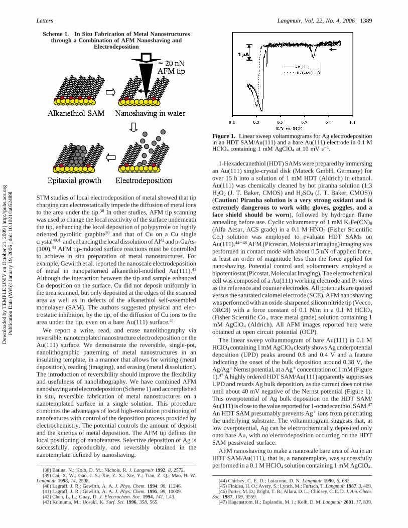
The linear sweep voltammogram of bare Au(111) in 0.1 MHClO4containing 1 mM AgClO4clearly shows Ag underpotentialdeposition (UPD) peaks around 0.8 and 0.4 V and a featureindicating the onset of the bulk deposition around 0.38 V, theAg/Ag+ Nernst potential, at a Ag+ concentration of 1 mM (Figure1).47A highly ordered HDT SAM/Au(111) apparently suppressesUPD and retards Ag bulk deposition, as the current does not riseuntil about 40 mV negative of the Nernst potential (Figure 1).This overpotential of Ag bulk deposition on the HDT SAM/Au(111) is close to the value reported for 1-octadecanthiol SAM.47
An HDT SAM presumably prevents Ag+ ions from penetratingthe underlying substrate. The voltammogram suggests that, atlow overpotential, Ag can be electrochemically deposited onlyonto bare Au, with no electrodeposition occurring on the HDTSAM passivated surface.
AFM nanoshaving to make a nanoscale bare area of Au in anHDT SAM/Au(111), that is, a nanotemplate, was successfullyperformed in a 0.1 M HClO4 solution containing 1 mM AgClO4.
(38) Batina, N.; Kolb, D. M.; Nichols, R. J.Langmuir1992, 8, 2572.(39) Cai, X. W.; Gao, J. S.; Xie, Z. X.; Xie, Y.; Tian, Z. Q.; Mao, B. W.
Langmuir1998, 14, 2508.(40) Lagraff, J. R.; Gewirth, A. A.J. Phys. Chem.1994, 98, 11246.(41) Lagraff, J. R.; Gewirth, A. A.J. Phys. Chem.1995, 99, 10009.(42) Chen, L. L.; Guay, D.J. Electrochem. Soc.1994, 141, L43.(43) Koinuma, M.; Uosaki, K.Surf. Sci.1996, 358, 565.
(44) Chidsey, C. E. D.; Loiacono, D. N.Langmuir1990, 6, 682.(45) Finklea, H. O.; Avery, S.; Lynch, M.; Furtsch, T.Langmuir1987, 3, 409.(46) Porter, M. D.; Bright, T. B.; Allara, D. L.; Chidsey, C. E. D.J. Am. Chem.
Soc.1987, 109, 3559.(47) Hagenstrom, H.; Esplandiu, M. J.; Kolb, D. M.Langmuir2001, 17, 839.
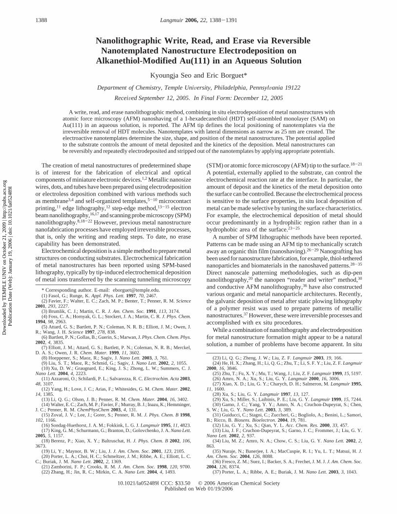
Scheme 1. In Situ Fabrication of Metal Nanostructuresthrough a Combination of AFM Nanoshaving and
Electrodeposition
Figure 1. Linear sweep voltammograms for Ag electrodepositionin an HDT SAM/Au(111) and a bare Au(111) electrode in 0.1 MHClO4 containing 1 mM AgClO4 at 10 mV s-1.
Letters Langmuir, Vol. 22, No. 4, 20061389
Dow
nloa
ded
by T
EM
PLE
UN
IV o
n O
ctob
er 2
1, 2
009
| http
://pu
bs.a
cs.o
rg
Pub
licat
ion
Dat
e (W
eb):
Jan
uary
19,
200
6 | d
oi: 1
0.10
21/la
0524
89l
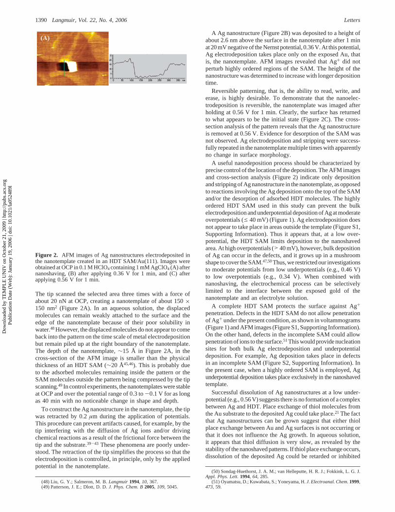
The tip scanned the selected area three times with a force ofabout 20 nN at OCP, creating a nanotemplate of about 150×150 nm2 (Figure 2A). In an aqueous solution, the displacedmolecules can remain weakly attached to the surface and theedge of the nanotemplate because of their poor solubility inwater.48However, the displaced molecules do not appear to comeback into the pattern on the time scale of metal electrodepositionbut remain piled up at the right boundary of the nanotemplate.The depth of the nanotemplate,∼15 Å in Figure 2A, in thecross-section of the AFM image is smaller than the physicalthickness of an HDT SAM (∼20 Å45,46). This is probably dueto the adsorbed molecules remaining inside the pattern or theSAM molecules outside the pattern being compressed by the tipscanning.49In control experiments, the nanotemplates were stableat OCP and over the potential range of 0.3 to-0.1 V for as longas 40 min with no noticeable change in shape and depth.
To construct the Ag nanostructure in the nanotemplate, the tipwas retracted by 0.2µm during the application of potentials.This procedure can prevent artifacts caused, for example, by thetip interfering with the diffusion of Ag ions and/or drivingchemical reactions as a result of the frictional force between thetip and the substrate.39-43 These phenomena are poorly under-stood. The retraction of the tip simplifies the process so that theelectrodeposition is controlled, in principle, only by the appliedpotential in the nanotemplate.
A Ag nanostructure (Figure 2B) was deposited to a height ofabout 2.6 nm above the surface in the nanotemplate after 1 minat 20 mV negative of the Nernst potential, 0.36 V. At this potential,Ag electrodeposition takes place only on the exposed Au, thatis, the nanotemplate. AFM images revealed that Ag+ did notperturb highly ordered regions of the SAM. The height of thenanostructure was determined to increase with longer depositiontime.
Reversible patterning, that is, the ability to read, write, anderase, is highly desirable. To demonstrate that the nanoelec-trodeposition is reversible, the nanotemplate was imaged afterholding at 0.56 V for 1 min. Clearly, the surface has returnedto what appears to be the initial state (Figure 2C). The cross-section analysis of the pattern reveals that the Ag nanostructureis removed at 0.56 V. Evidence for desorption of the SAM wasnot observed. Ag electrodeposition and stripping were success-fully repeated in the nanotemplate multiple times with apparentlyno change in surface morphology.
A useful nanodeposition process should be characterized byprecise control of the location of the deposition. The AFM imagesand cross-section analysis (Figure 2) indicate only depositionand stripping of Ag nanostructure in the nanotemplate, as opposedto reactions involving the Ag deposition onto the top of the SAMand/or the desorption of adsorbed HDT molecules. The highlyordered HDT SAM used in this study can prevent the bulkelectrodeposition and underpotential deposition of Ag at moderateoverpotentials (e 40 mV) (Figure 1). Ag electrodeposition doesnot appear to take place in areas outside the template (Figure S1,Supporting Information). Thus it appears that, at a low over-potential, the HDT SAM limits deposition to the nanoshavedarea. At high overpotentials (> 40 mV), however, bulk depositionof Ag can occur in the defects, and it grows up in a mushroomshape to cover the SAM.47,50Thus, we restricted our investigationsto moderate potentials from low underpotentials (e.g., 0.46 V)to low overpotentials (e.g., 0.34 V). When combined withnanoshaving, the electrochemical process can be selectivelylimited to the interface between the exposed gold of thenanotemplate and an electrolyte solution.
A complete HDT SAM protects the surface against Ag+
penetration. Defects in the HDT SAM do not allow penetrationof Ag+ under the present condition, as shown in voltammograms(Figure 1) and AFM images (Figure S1, Supporting Information).On the other hand, defects in the incomplete SAM could allowpenetration of ions to the surface.51This would provide nucleationsites for both bulk Ag electrodeposition and underpotentialdeposition. For example, Ag deposition takes place in defectsin an incomplete SAM (Figure S2, Supporting Information). Inthe present case, when a highly ordered SAM is employed, Agunderpotential deposition takes place exclusively in the nanoshavedtemplate.
Successful dissolution of Ag nanostructures at a low under-potential (e.g., 0.56 V) suggests there is no formation of a complexbetween Ag and HDT. Place exchange of thiol molecules fromthe Au substrate to the deposited Ag could take place.21 The factthat Ag nanostructures can be grown suggest that either thiolplace exchange between Au and Ag surfaces is not occurring orthat it does not influence the Ag growth. In aqueous solution,it appears that thiol diffusion is very slow, as revealed by thestability of the nanoshaved patterns. If thiol place exchange occurs,dissolution of the deposited Ag could be retarded or inhibited
(48) Liu, G. Y.; Salmeron, M. B.Langmuir1994, 10, 367.(49) Patterson, J. E.; Dlott, D. D.J. Phys. Chem. B2005, 109, 5045.
(50) Sondag-Huethorst, J. A. M.; van Helleputte, H. R. J.; Fokkink, L. G. J.Appl. Phys. Lett.1994, 64, 285.
(51) Oyamatsu, D.; Kuwabata, S.; Yoneyama, H.J. Electroanal. Chem.1999,473, 59.
Figure 2. AFM images of Ag nanostructures electrodeposited inthe nanotemplate created in an HDT SAM/Au(111). Images wereobtained at OCP in 0.1 M HClO4 containing 1 mM AgClO4 (A) afternanoshaving, (B) after applying 0.36 V for 1 min, and (C) afterapplying 0.56 V for 1 min.
1390 Langmuir, Vol. 22, No. 4, 2006 Letters
Dow
nloa
ded
by T
EM
PLE
UN
IV o
n O
ctob
er 2
1, 2
009
| http
://pu
bs.a
cs.o
rg
Pub
licat
ion
Dat
e (W
eb):
Jan
uary
19,
200
6 | d
oi: 1
0.10
21/la
0524
89l
by the formation of a SAM on the Ag nanostructure.21,52However,the cross-sectional analysis in Figure 2C reveals that a Agnanostructure in the template clearly dissolved in 1 min.
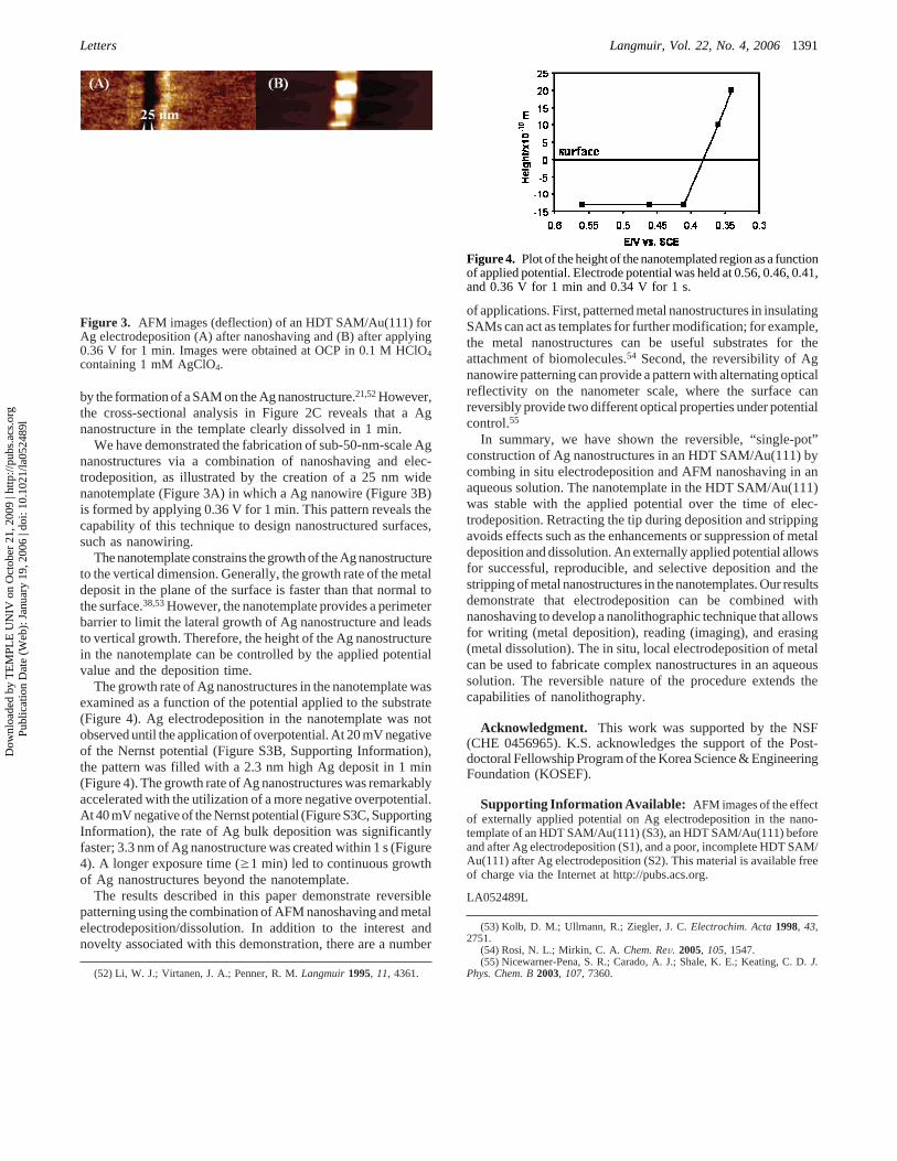
We have demonstrated the fabrication of sub-50-nm-scale Agnanostructures via a combination of nanoshaving and elec-trodeposition, as illustrated by the creation of a 25 nm widenanotemplate (Figure 3A) in which a Ag nanowire (Figure 3B)is formed by applying 0.36 V for 1 min. This pattern reveals thecapability of this technique to design nanostructured surfaces,such as nanowiring.
The nanotemplate constrains the growth of the Ag nanostructureto the vertical dimension. Generally, the growth rate of the metaldeposit in the plane of the surface is faster than that normal tothe surface.38,53However, the nanotemplate provides a perimeterbarrier to limit the lateral growth of Ag nanostructure and leadsto vertical growth. Therefore, the height of the Ag nanostructurein the nanotemplate can be controlled by the applied potentialvalue and the deposition time.
The growth rate of Ag nanostructures in the nanotemplate wasexamined as a function of the potential applied to the substrate(Figure 4). Ag electrodeposition in the nanotemplate was notobserved until the application of overpotential. At 20 mV negativeof the Nernst potential (Figure S3B, Supporting Information),the pattern was filled with a 2.3 nm high Ag deposit in 1 min(Figure 4). The growth rate of Ag nanostructures was remarkablyaccelerated with the utilization of a more negative overpotential.At 40 mV negative of the Nernst potential (Figure S3C, SupportingInformation), the rate of Ag bulk deposition was significantlyfaster; 3.3 nm of Ag nanostructure was created within 1 s (Figure4). A longer exposure time (g1 min) led to continuous growthof Ag nanostructures beyond the nanotemplate.
The results described in this paper demonstrate reversiblepatterning using the combination of AFM nanoshaving and metalelectrodeposition/dissolution. In addition to the interest andnovelty associated with this demonstration, there are a number
of applications. First, patterned metal nanostructures in insulatingSAMs can act as templates for further modification; for example,the metal nanostructures can be useful substrates for theattachment of biomolecules.54 Second, the reversibility of Agnanowire patterning can provide a pattern with alternating opticalreflectivity on the nanometer scale, where the surface canreversibly provide two different optical properties under potentialcontrol.55
In summary, we have shown the reversible, “single-pot”construction of Ag nanostructures in an HDT SAM/Au(111) bycombing in situ electrodeposition and AFM nanoshaving in anaqueous solution. The nanotemplate in the HDT SAM/Au(111)was stable with the applied potential over the time of elec-trodeposition. Retracting the tip during deposition and strippingavoids effects such as the enhancements or suppression of metaldeposition and dissolution. An externally applied potential allowsfor successful, reproducible, and selective deposition and thestripping of metal nanostructures in the nanotemplates. Our resultsdemonstrate that electrodeposition can be combined withnanoshaving to develop a nanolithographic technique that allowsfor writing (metal deposition), reading (imaging), and erasing(metal dissolution). The in situ, local electrodeposition of metalcan be used to fabricate complex nanostructures in an aqueoussolution. The reversible nature of the procedure extends thecapabilities of nanolithography.
Acknowledgment. This work was supported by the NSF(CHE 0456965). K.S. acknowledges the support of the Post-doctoral Fellowship Program of the Korea Science & EngineeringFoundation (KOSEF).
Supporting Information Available: AFM images of the effectof externally applied potential on Ag electrodeposition in the nano-template of an HDT SAM/Au(111) (S3), an HDT SAM/Au(111) beforeand after Ag electrodeposition (S1), and a poor, incomplete HDT SAM/Au(111) after Ag electrodeposition (S2). This material is available freeof charge via the Internet at http://pubs.acs.org.
LA052489L
(52) Li, W. J.; Virtanen, J. A.; Penner, R. M.Langmuir1995, 11, 4361.
(53) Kolb, D. M.; Ullmann, R.; Ziegler, J. C.Electrochim. Acta1998, 43,2751.
(54) Rosi, N. L.; Mirkin, C. A.Chem. ReV. 2005, 105, 1547.(55) Nicewarner-Pena, S. R.; Carado, A. J.; Shale, K. E.; Keating, C. D.J.
Phys. Chem. B2003, 107, 7360.
Figure 3. AFM images (deflection) of an HDT SAM/Au(111) forAg electrodeposition (A) after nanoshaving and (B) after applying0.36 V for 1 min. Images were obtained at OCP in 0.1 M HClO4containing 1 mM AgClO4.
Figure 4. Plot of the height of the nanotemplated region as a functionof applied potential. Electrode potential was held at 0.56, 0.46, 0.41,and 0.36 V for 1 min and 0.34 V for 1 s.
Letters Langmuir, Vol. 22, No. 4, 20061391
Dow
nloa
ded
by T
EM
PLE
UN
IV o
n O
ctob
er 2
1, 2
009
| http
://pu
bs.a
cs.o
rg
Pub
licat
ion
Dat
e (W
eb):
Jan
uary
19,
200
6 | d
oi: 1
0.10
21/la
0524
89l