multinozzle emitter arrays for nanoelectrospray mass...
TRANSCRIPT
Published: July 05, 2011
r 2011 American Chemical Society 6082 dx.doi.org/10.1021/ac2011813 |Anal. Chem. 2011, 83, 6082–6089
ARTICLE
pubs.acs.org/ac
Multinozzle Emitter Arrays for Nanoelectrospray Mass SpectrometryPan Mao,† Hung-Ta Wang,§ Peidong Yang,‡,§ and Daojing Wang*,†
†Life Sciences Division, ‡Materials Sciences Division, Lawrence Berkeley National Laboratory, Berkeley, California 94720, United States§Department of Chemistry, University of California, Berkeley, California 94720, United States
bS Supporting Information
ABSTRACT:
Mass spectrometry (MS) is the enabling technology for proteomics and metabolomics. However, dramatic improvements in bothsensitivity and throughput are still required to achieve routine MS-based single cell proteomics and metabolomics. Here, we reportthe silicon-basedmonolithic multinozzle emitter array (MEA) and demonstrate its proof-of-principle applications in high-sensitivityand high-throughput nanoelectrospray mass spectrometry. OurMEA consists of 96 identical 10-nozzle emitters in a circular array ona 3 in. silicon chip. The geometry and configuration of the emitters, the dimension and number of the nozzles, and the micropillararrays embedded in themain channel can be systematically and precisely controlled during themicrofabrication process. Combiningelectrostatic simulation and experimental testing, we demonstrated that sharpened-end geometry at the stem of the individualmultinozzle emitter significantly enhanced the electric fields at its protruding nozzle tips, enabling sequential nanoelectrospray forthe high-density emitter array. We showed that electrospray current of the multinozzle emitter at a given total flow rate wasapproximately proportional to the square root of the number of its spraying-nozzles, suggesting the capability of high MS sensitivityfor multinozzle emitters. Using a conventional Z-spray mass spectrometer, we demonstrated reproducible MS detection of peptidesand proteins for serial MEA emitters, achieving sensitivity and stability comparable to the commercial capillary emitters. Our robustsilicon-based MEA chip opens up the possibility of a fully integrated microfluidic system for ultrahigh-sensitivity and ultrahigh-throughput proteomics and metabolomics.
Single cell omics unifies biology and technology and hasbecome a new frontier.1 For mass spectrometry (MS)-based
single cell proteomics and metabolomics, proof-of-principle ex-periments have been performed to characterize peptides andmetabolites using matrix-assisted laser desorption ionization(MALDI)-MS2�4 and electrospray ionization (ESI)-MS.5,6 How-ever, samples were processed individually offline and coverageof proteome and metabolome was limited in these studies.Key challenges still remain. First, further improvement in detec-tion sensitivity; second, extremely efficient processing of minuteamount of samples, down to a single cell; and third, high-through-put analysis in a cost-effective manner so that a large number ofindividual cells can be analyzed to achieve statistical significance.Since ESI-MS,7 particularly nano-ESI-MS,8 is the dominant softionization method for analyzing peptides and proteins, a fullyintegrated microfluidic front-end system interfaced with nano-ESI-MS may serve as a unified platform to address the above-mentioned challenges. Microfluidics enables efficient sample
manipulation and processing down to the picoliter even femto-liter range.9 Furthermore, the robustness and adaptability ofmicrofabrication processes enables production of massively par-allel functional modules on a single chip for high-throughputanalysis.
In fact, one of the actively pursued areas in MS has beento implement the high-quality interface between microchips andmass spectrometers.10 Emitters based on polymericmaterials,11�15
glass,16,17 and silicon using out-of-plane processes18 had beenfabricated. However, hydrophobic polymers have inherently un-desirable properties for electrospray, such as a strong affinity toproteins and peptides and incompatibility with certain organicsolvents; glass substrates are difficult to fabricate for complex struc-tures; and out-of-plane strategy is critically limited in producing
Received: May 12, 2011Accepted: June 21, 2011
6083 dx.doi.org/10.1021/ac2011813 |Anal. Chem. 2011, 83, 6082–6089
Analytical Chemistry ARTICLE
monolithically integrated devices. Efforts in the field have ledto two commercial MS-chips: Agilent’s HPLC-chip made ofpolyimide andWaters’ “nanoTile” chipmade of ceramic. However,these devices have been developed for routine liquid chromato-graphy�tandem mass spectrometry (LC�MS/MS) applicationsand lack high-throughput capabilities. Their wide adoption by theresearch community remains to be seen because of their high costsand requirements for vendor-designated mass spectrometers.
Performing high-throughput ESI-MS remains a challenge be-cause MS itself has a high capital and operational cost, limiting itsscalability. Furthermore, MS is a serial detection system typicallycapable of analyzing one sample at a time. Hence, there is a trem-endous demand in developing high-throughput MS front-endsystems. One approach is to implement multiple LC systems inparallel that are coupled to a single MS detector. This reduces MSdown time during sample injection and loading and hence im-proves MS usage efficiency. Although in its infancy, the multiple-sprayer platform has been recognized as a potential high-qualityinterface for high-sensitivity and high-throughput ESI-MS.19
“Simultaneous multiple electrosprays” have been achieved with abundle of fused silica capillaries20 and photonic fibers21 toimprove MS sensitivity. However, the former has a size in therange of millimeters to centimeters and is not suitable forconventional mass spectrometers. Furthermore, neither of themis amenable for monolithic integration on a microchip. “Sequen-tial multiple electrosprays” using multichannel,22,23 multitrack,24
out-of-plane multiple nozzles,18 and gated multi-inlets,25 havebeen implemented for high-throughput MS. In this approach,each sample is processed by a different front-end system (e.g., LC
orCE) connected to an individual sprayer. This eliminates samplecross-contamination and allows efficient coupling between var-ious components to reduce the dead volume/time. However, thesedevices also have intrinsic limitations in monolithic integration.
We had previously developed microfabricated monolithic multi-nozzle emitters (M3 emitters) for nanoelectrospray mass spectro-metry.26 Our in-plane strategy allows ease and flexibility in design,integration, and interfacing to MS. However, the high operatingvoltage (g4.5 kV) required even for the low-nozzle-numberM3 emitters (up to 5 nozzles) to achieve stable electrosprayremained problematic. This prevented us from implementing high-nozzle-numberM3 emitters (>10 nozzles).Herein, we report a novelapproach to create monolithic multinozzle emitter arrays (MEAs)for nanoelectrospray mass spectrometry. We demonstrate two keytechnical breakthroughs in these devices. First, high-density (up to 96)emitters were constructed in a circular array format on a 3 in. siliconchip (i.e., MEA chip), utilizing the concept of “sequential multipleelectrosprays” and hence enabling high-throughput applications.Second, sharpened-end emitters with a large number of nozzles(up to 40) per emitter were engineered on the MEA chip, utilizingthe concept of “simultaneous multiple electrosprays” and henceenabling high-sensitivityMSdetections.We further demonstrate theapplicability of our MEA chips for metabolomics and proteomicsapplications via MS analyses of peptides and tryptic digests.
’EXPERIMENTAL SECTION
Design and Fabrication of MEA Chips. MEA chips weredesigned using the L-Edit software (v15, Tanner Research Inc.).
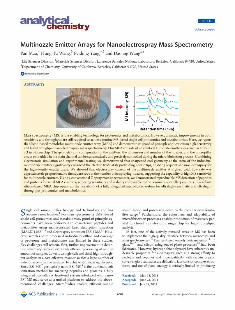
Figure 1. Multinozzle emitter array chip: (a) A plan view of a 96-emitter array chip. The green circles represent through-holes for sample injection. Thered lines represent microfluidic channels of 400 μm in width and 10 μm in depth, which can be embedded with ordered micropillar arrays. The bluecurves represent the sharpened features of the multinozzle emitters. (b) High-definition photograph of a 3 in. MEA chip fabricated from 4 in. siliconwafers. The device is connected to 96 silica capillaries via the PTFE tubing. (c, d) SEM images of 10-nozzle emitters with different magnifications. Eachemitter consists of a linear 10-nozzle array, with a conduit length of around 100 μm and a cross-section of 10 μm� 10 μm, protruding out from a hollowsilicon sliver. The internozzle spacing is 40μm. (e) SEM images of micropillar arrays within amain channel. The pillars are 10μmdeepwith a diameter of4.5 μm and spaced by 5.5 μm. They are arranged according to an equilateral triangular grid. Boxes in part a indicate the corresponding zoom-in regionsfor parts c and e, respectively.
6084 dx.doi.org/10.1021/ac2011813 |Anal. Chem. 2011, 83, 6082–6089
Analytical Chemistry ARTICLE
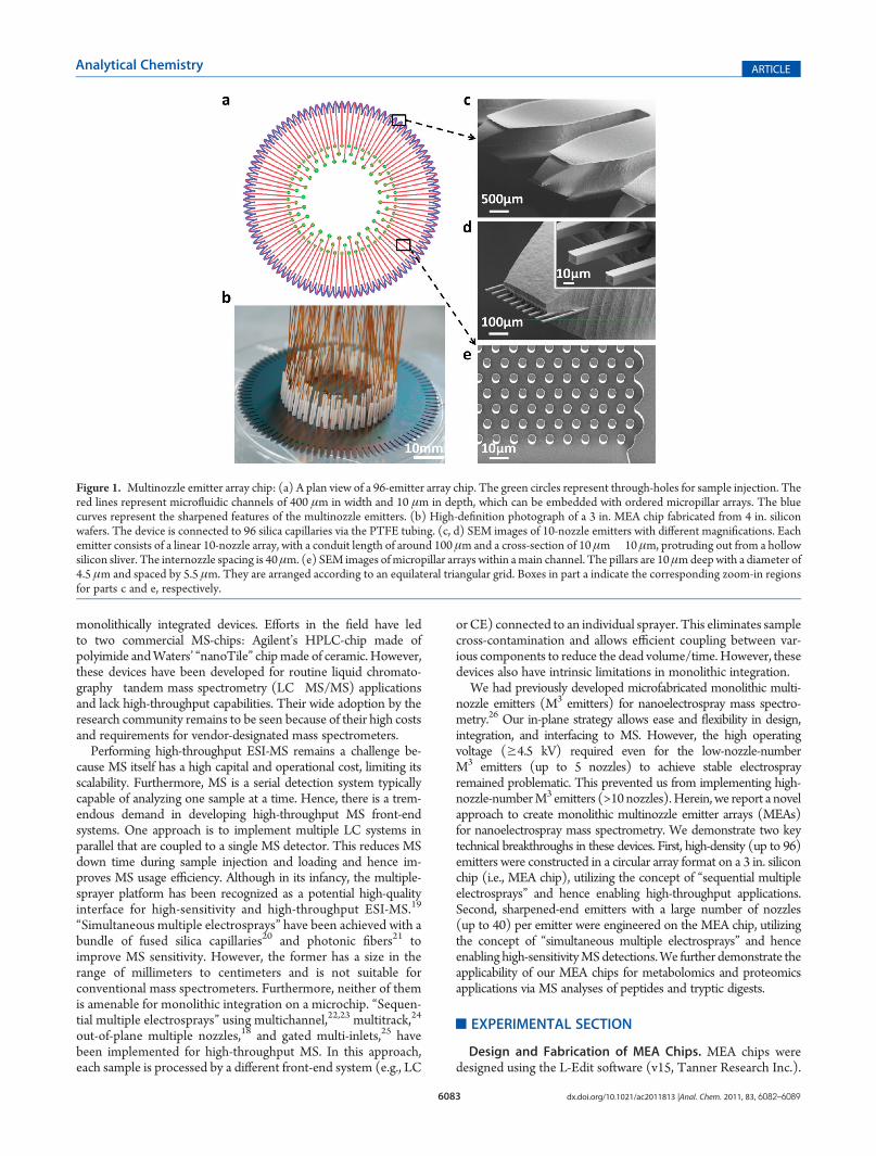
The procedures to fabricate the MEA chips were improved fromthose for M3 emitters26 and involved 9 major steps (SupplementFigure 1a-i in the Supporting Information). First, we performedstandard photolithography and deep reactive ion etching (DRIE)to pattern and produce channels (with micropillar arrays ifneeded) and emitters on a 4 in. silicon wafer (a�c). Then, weperformed second-layer photolithography andDRIE to define andcreate access holes with a second film mask (d). Next, we per-formed thermal fusion bonding between the patterned wafer andanother clean wafer (e), followed by wet oxidation to grow a thickoxide of ∼1 μm on all silicon surfaces including the sealedchannels/emitters (f). Afterward, we performed another photo-lithography and through-wafer etching steps to sharpen theemitters (left- and right-side, Figure 1 and Figure 2) and releasethe chip from the wafer (g). Subsequently, we sharpened the othertwo sides (top and bottom, Figure 1 and Figure 2) of the emittersby mechanically polishing the emitter stem with the sand paper(h). Finally, we etched away silicon at the sharpened end of theemitters by selective XeF2 etching (i). This final step ended upwith protruding nozzlesmade of SiO2. The fabricated devices wereexamined by optical microscopy using a Reichert-Jung Polylite 88microscope (Reichert Microscope Services) and by scanning elec-tron microscopy using a JEOL 6340F FEG-SEM (JEOL Ltd.).Electrostatic Simulations of MEA Emitters. The multiphy-
sics modeling and simulation software COMSOL (v4.1, COM-SOL Inc.) was used to simulate electric fields of 10-nozzle MEAemitters with flat-end, two-side sharpened-end, and four-sidesharpened-end features. For simplicity, we did not take intoaccount the presence of complex dynamic gas/fluid behaviorsduring the actual electrospray process and only considered static
electric fields on MEA emitters relative to the Z-spray samplecone of the Q-TOF API US mass spectrometer (Waters Corp.).Furthermore, we simulated a quadrant instead of the wholedevice to reduce the dimensions of modeling. The 3D geometrywas constructed with the parameters similar to the actual experi-mental setup. Calculated electric fields were analyzed by 3D sliceplots on the central plane (z = 0). The detailed simulationparameters are provided in the Supporting Information.Electrospray CurrentMeasurement ofMEAEmitters.Total
electrospray currents were measured using the Keithley 6487Picoammeter with built-in data acquisition capabilities (KeithleyInstruments). The experimental setup is shown in SupplementFigure 3 in the Supporting Information and similar to what hadbeen described.27 Electrospray images were taken using aWatersnanoflow camera kit equipped with a MLH-10� microscope(Computar) and using a digital camera Nikon 3700 (Nikon Inc.)mounted on a 6 � 16 monocular (Specwell Corp.).Nanoelectrospray Mass Spectrometry. All electrospray MS
experiments were performed on a hybrid quadrupole/orthogo-nal Q-TOF API US mass spectrometer (Waters Corp.) as de-scribed.28 The MEA chip was mounted on the voltage stand andmanually rotated every 3�4� for each adjacent emitter. MEAchips were connected with fused silica capillaries (o.d.∼360 μm,i.d.∼100 μm) by polytetrafluoroethylene (PTFE) tubing whoseouter diameter (o.d.) matches the i.d. of access holes. Torr Sealepoxy (Agilent Technologies) was applied to permanently sealthe connection which could withstand a pressure of more than100 psi. An aluminum conductive tape (3M) provided the directelectric contact between the voltage stand and the conductive Si-based MEA chip.
Figure 2. Simulated electric fields onMEA chips. Three-dimensional electrostatic modeling for representative flat-end (a), two-side sharpened-end (b),and four-side sharpened-end (c) emitters is shown. Every emitter contains 10 nozzles each with a cross-section of 10 μm� 10 μm. The 3D slice plots ofelectric fields on the three types of emitters (i), their relative position to the ion cone (ii), and the close-up views on the central emitters designated by thewhite arrows (iii) are shown. The voltage for the mass spectrometer ion cone and MEA chip is set to be 40 and 3000 V, respectively. The maximummagnitude of the electric fields (volt/meter) at the nozzle tip of each type of emitters is highlighted on the scale bars individually (iii).
6085 dx.doi.org/10.1021/ac2011813 |Anal. Chem. 2011, 83, 6082–6089
Analytical Chemistry ARTICLE
Liquid Chromatography�MS/MS. LC�MS/MS analysiswas performed using a capillary liquid chromatography system(CapLC) (Waters Corp.) interfaced with a Q-TOF API USmassspectrometer as described.28 LC runs using the same C18column were performed sequentially and independently for in-dividual multinozzle emitters. Peptides eluted from the columnwere directed through a connecting PTFE tubing (i.d. ∼75 μm;o.d. ∼1.6 mm) to the Picotips or MEA emitters for nanoelec-trospray mass spectrometry. Mass spectra were processed usingthe MassLynx 4.0 SP4 software. Proteins were identified byMascot (http://www.matrixscience.com) using the MS/MSpeak lists exported from the MassLynx. More experimental de-tails including safety considerations are described in the Support-ing Information.
’RESULTS AND DISCUSSION
Multinozzle Emitter Arrays.We developed MEAs consistingof 96 identical multinozzle emitters in a circular array, uniformlydistributed on the periphery of a 3 in. silicon chip (Figure 1a,b).We designed the array layout and interemitter spacing in such away to achieve the best electrospray performance possible whilemaximizing the number of emitters on the device. Notably, ourfabrication processes are amendable for higher-number emitterarrays, e.g., 384 emitters on 6 in. Si wafers.We utilized sharpened-end features at the four edges (left,
right, top, and bottom) of each emitter in order to obtainenhanced electric fields (discussed in the next section). Eachemitter was connected to off-chip components via capillariesthrough its access hole. This is a straightforward design compa-tible with the majority of the microfluidic systems. Figure 1bshows a representative optical image of a MEA chip with 96emitters individually connected to capillaries for sample injec-tion. Parts c, d, and e of Figure 1 show SEM images for threeadjacent emitters, a single 10-nozzle emitter, and the micropillararrays monolithically imbedded in the main channel of eachemitter, respectively. The micropillar arrays will be utilized in thefuture for online digestion (e.g., with trypsin coating) or separa-tion (e.g., with C18 or C4 coating) after surface derivatizationusing silylation chemistry.We fabricated emitters with varied nozzle numbers, cross
sections, and wall-thickness. Supplement Figure 2 shows threerepresentative sharpened-end emitters with a nozzle cross-section ranging from 10 μm � 10 μm to 2 μm � 2.5 μm, andthe corresponding nozzle number per emitter from 1 to 40.We were able to fabricate nozzles with a cross-section downto∼800 nm�800 nm (data not shown), but a significant increaseof back pressure29 prevented us from utilizing these small nozzlesfor ESI-MS (see Supporting Information formore discussion).Wehave mainly examined the performance of multinozzle emitterswith a nozzle cross-section of∼10 μm� 10 μm in this work. Thepotential of using smaller nozzles will be explored in the future.We achieved a fabrication yield close to 100% for MEA
emitters due to the significantly improved microfabricationprocesses. For our M3 emitters, sealed main channels wereopened up by mechanical sawing, which resulted in seriousclogging.26 The fabrication of MEA emitters did not involvethe mechanical dicing step. Instead, main channels were openedup by deep reactive ion etching, which is a dry etching processthat does not introduce any particles into the main channels. Themechanical polishing step with the sand paper (step h) typicallygenerates particles larger than the nozzle sizes (e.g., 10 μm),
which are removed by piranha cleaning. Therefore, our newprocedures dramatically reduced channel clogging and improveddevice yields. Additionally, the connection between the MEAchip and outside liquid sources can be improved by building acustom-made manifold which mechanically assembles the chipwith tubings, O-rings, and/or gaskets. This manifold can with-stand high pressures and be reused and also minimizes deadvolumes.Electric Fields on the Multinozzle Emitter Arrays. We
utilized a 3D electrostatic simulator to examine the effects ofsharpened-end features on the electric fields of emitters. Threetypes of emitters with the same number of nozzles (i.e., 10)including those for flat-end (Figure 2a), two-side sharpened-end(Figure 2b), and four-side sharpened-end (Figure 2c) werecompared. The electric fields were much stronger at the nozzletips than in the other regions of the emitters for all three cases.However, the maximum of the electric fields at the nozzle tipssignificantly increased from 3.7 � 106 V/m for the flat-endemitters to 6.6 � 106 V/m for the four-side sharpened-endemitters. For each emitter, we observed higher electric fields at
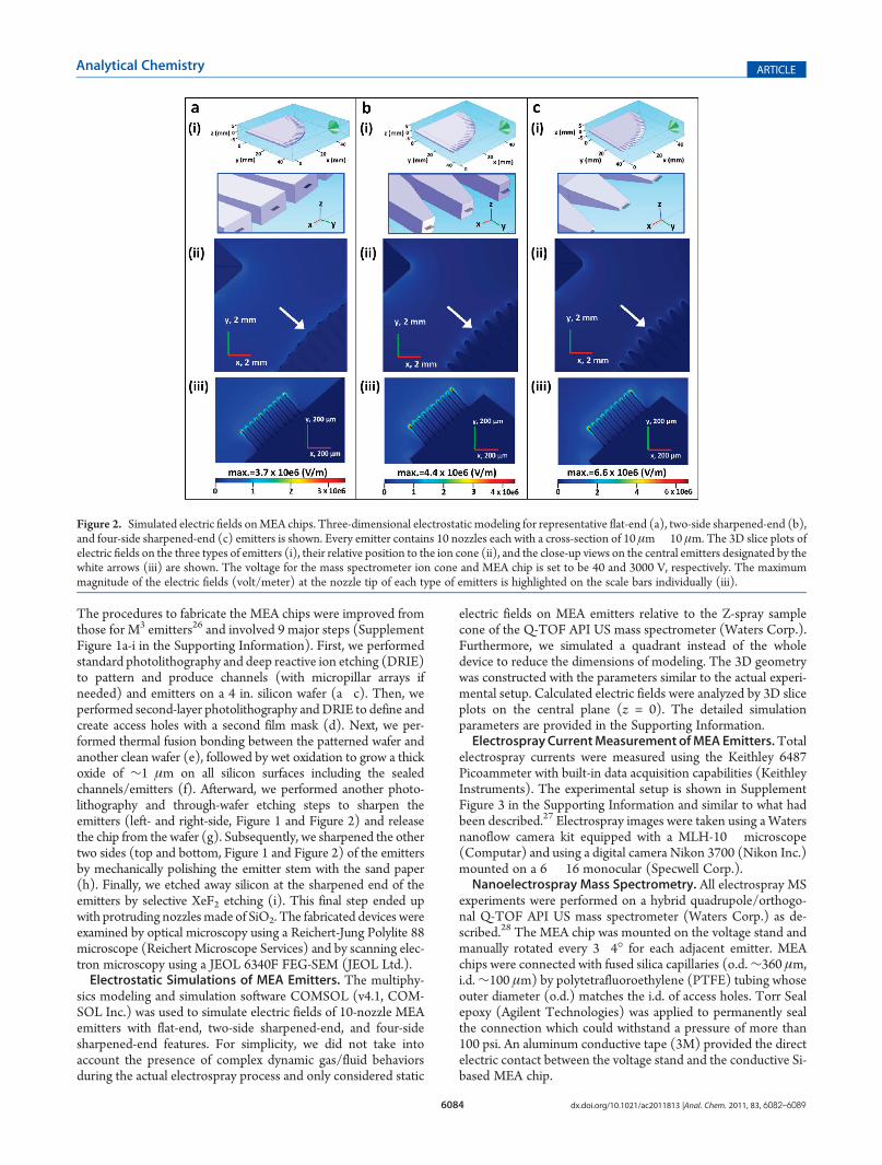
Figure 3. Electrospray modes onMEA chips. (a) Comparison betweenelectrostatic simulation and electrospray on a MEA chip: (a-i) repre-sentative values of the simulated electric fields at the center of eachnozzle, on a four-side sharpened-end 10-nozzle MEA emitter. Thevoltages and the relative geometry for the ion cone and the MEA chipare the same as in Figure 2c. (a-ii) Corresponding electrospray imagesfor the 10-nozzle MEA emitter. Electrospray was performed using50% methanol/H2O + 0.1% formic acid at a flow rate of 3.0 μL/min.(b) Electrospray images of 1-nozzle MEA emitters at the flow rate of0.6μL/min, showing the (b-i) pulsating (2.3 kV), (b-ii) cone-jet (2.7 kV),and (b-iii) multi-jet (3.3 kV) modes. (c) Electrospray images of 10-nozzle MEA emitters at the flow rate of 1.0 μL/min, showing the (c-i)pulsating, (c-ii) cone-jet, and (c-iii) “multi-jet” modes at indicatedvoltages. The images were taken using the setup for electrospray currentmeasurements. The solvent was 50% methanol/H2O + 1% acetic acid.All nozzles have a cross-section of 10 μm � 10 μm. Scale bars in partsa�c are 500 μm.
6086 dx.doi.org/10.1021/ac2011813 |Anal. Chem. 2011, 83, 6082–6089
Analytical Chemistry ARTICLE
the tips of the periphery nozzles than those of the interior ones.In particular, there was a gradual increase from the center to theedge of the linear nozzle array, with amaximum increase of 48.7%from the center nozzle (3.9 � 106) to the edge nozzle (5.8 �106) for the four-side sharpened-end emitters (Figure 2c(iii) andFigure 3a). This was due to the linear format of the nozzle array,the position of the nozzle array relative to the ion cone (Z-spray),the nozzle�nozzle interactions (shielding effects),30 and theinteractions between the emitter stem and the nozzles on the twoedges (i.e., the edge effects). Consistently, we observed evenhigher electric fields at the corner of the nozzles on two edges, i.e.,6.6� 106 (left corner, not labeled) vs 5.8� 106 (center, labeled)for the leftmost nozzle and 6.1 � 106 (right corner, not labeled)vs 5.7 � 106 (center, labeled) for the rightmost nozzle, respec-tively (Figure 3a). We further confirmed the simulated patternof the electric fields experimentally. As demonstrated by theelectrospray images of a corresponding 10-nozzle MEA emitter,the spray plumes showed a clear edge effect for the outmostnozzles while relative homogeneity among the inner nozzles(Figure 3b).Although enhancement of electric fields at sharp tips is a
known phenomenon, ours is one of the first examples showing
increased electric fields at the nozzles through sharpening theemitter stems instead of the nozzles themselves for Si-baseddevices. The protruding feature of the nozzles prevented samplewetting on the emitter surface, while the sharpening of theemitter stems ensured sufficient electric fields for Taylor coneformation. It is expected that additional improvement could beachieved by optimizing the shape of the nozzle support (e.g.,sharpening angles for four sides) and the 3D layout of the nozzles(e.g., a circular array). The same modeling strategy is applicablefor rational design of microfluidic modules.Electrospray Currents of Multinozzle Emitter Arrays. We
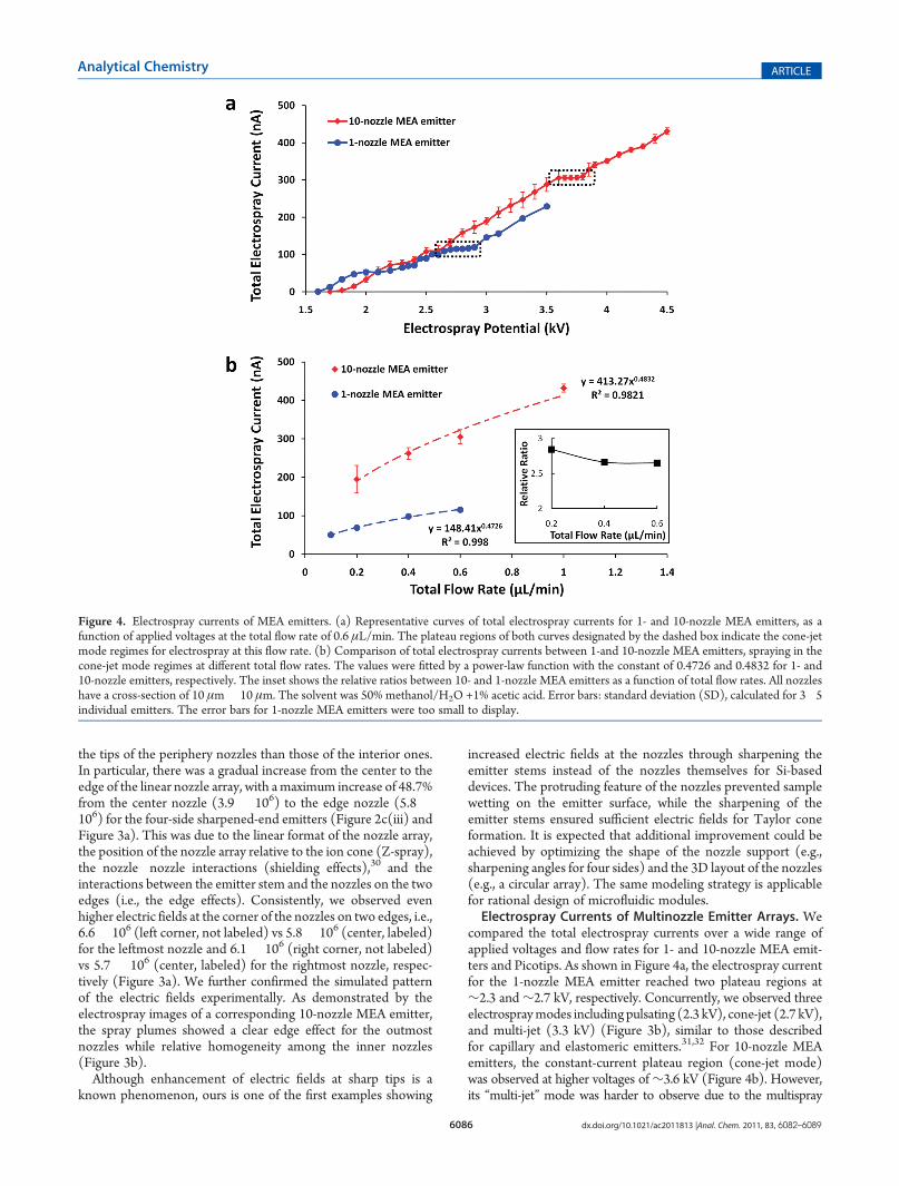
compared the total electrospray currents over a wide range ofapplied voltages and flow rates for 1- and 10-nozzle MEA emit-ters and Picotips. As shown in Figure 4a, the electrospray currentfor the 1-nozzle MEA emitter reached two plateau regions at∼2.3 and∼2.7 kV, respectively. Concurrently, we observed threeelectrospraymodes including pulsating (2.3 kV), cone-jet (2.7 kV),and multi-jet (3.3 kV) (Figure 3b), similar to those describedfor capillary and elastomeric emitters.31,32 For 10-nozzle MEAemitters, the constant-current plateau region (cone-jet mode)was observed at higher voltages of∼3.6 kV (Figure 4b). However,its “multi-jet” mode was harder to observe due to the multispray
Figure 4. Electrospray currents of MEA emitters. (a) Representative curves of total electrospray currents for 1- and 10-nozzle MEA emitters, as afunction of applied voltages at the total flow rate of 0.6 μL/min. The plateau regions of both curves designated by the dashed box indicate the cone-jetmode regimes for electrospray at this flow rate. (b) Comparison of total electrospray currents between 1-and 10-nozzle MEA emitters, spraying in thecone-jet mode regimes at different total flow rates. The values were fitted by a power-law function with the constant of 0.4726 and 0.4832 for 1- and10-nozzle emitters, respectively. The inset shows the relative ratios between 10- and 1-nozzle MEA emitters as a function of total flow rates. All nozzleshave a cross-section of 10 μm� 10 μm. The solvent was 50% methanol/H2O +1% acetic acid. Error bars: standard deviation (SD), calculated for 3�5individual emitters. The error bars for 1-nozzle MEA emitters were too small to display.
6087 dx.doi.org/10.1021/ac2011813 |Anal. Chem. 2011, 83, 6082–6089
Analytical Chemistry ARTICLE
nature of the multinozzle emitters (Figure 3c). On the otherhand, we observed comparable electrospray currents for 1-nozzleMEA emitter and Picotips under the same conditions, althoughthere was no clear plateau region for Picotips (data not shown).We next tested whether our multinozzle emitters followed the
square root n relationship, i.e., the total electrospray current fromthemultielectrosprays in the cone-jet mode is proportional to thesquare root of the number (n) of sprays (nozzles).27,32 Wemeasured the dependence between total electrospray currentand applied voltages for 1- and 10-nozzle MEA emitters at giventotal flow rates, shown in Figure 4a for 0.6 μL/min. We thendetermined the electrospray current for a particular total flowrate at the plateau region corresponding to the cone-jet mode. Asshown in Figure 4b, the electrospray currents from both 1- and10-nozzle MEA emitters fitted a power of the total flow rate, withthe power constant of 0.47 and 0.48, respectively. This wasconsistent with the square root relationship between spraycurrents and total flow rates. Furthermore, at a given total flowrate, the ratio of electrospray currents between 10- and 1-nozzleMEA emitters was calculated to be 2.65�2.85 for the total flowrates of 0.2�0.6 μL/min (Figure 4b, insert), which was 10�20%less than the predicted theoretical ratio of 3.16, i.e., the squareroot of 10 (nozzles).27,32 The discrepancy might be due to theinhomogeneity among the 10 nozzles as exemplified by theirelectric field distribution (Figure 3a) as well as the much strongerinternozzle interactions for 10-nozzle MEA emitters in compar-ison to a bundle of multiple capillary emitters.32 In fact, both thesize (a cross-section of ∼10 μm � 10 μm) and internozzle
spacing (∼40 μm) of MEA emitters were significantly smallerthan those of the bundle of fused silica capillaries (i.d. ∼19 μmand the intercapillary spacing of ∼500 μm, respectively). Inaddition, there were interemitter interactions on MEA chips.Nevertheless, the significant increase of electrospray currents in10-nozzle MEA emitters suggested the feasibility of achievingeven higher MS sensitivity for multinozzle emitters with largernozzle numbers.High-Throughput Mass Spectrometry Using Multinozzle
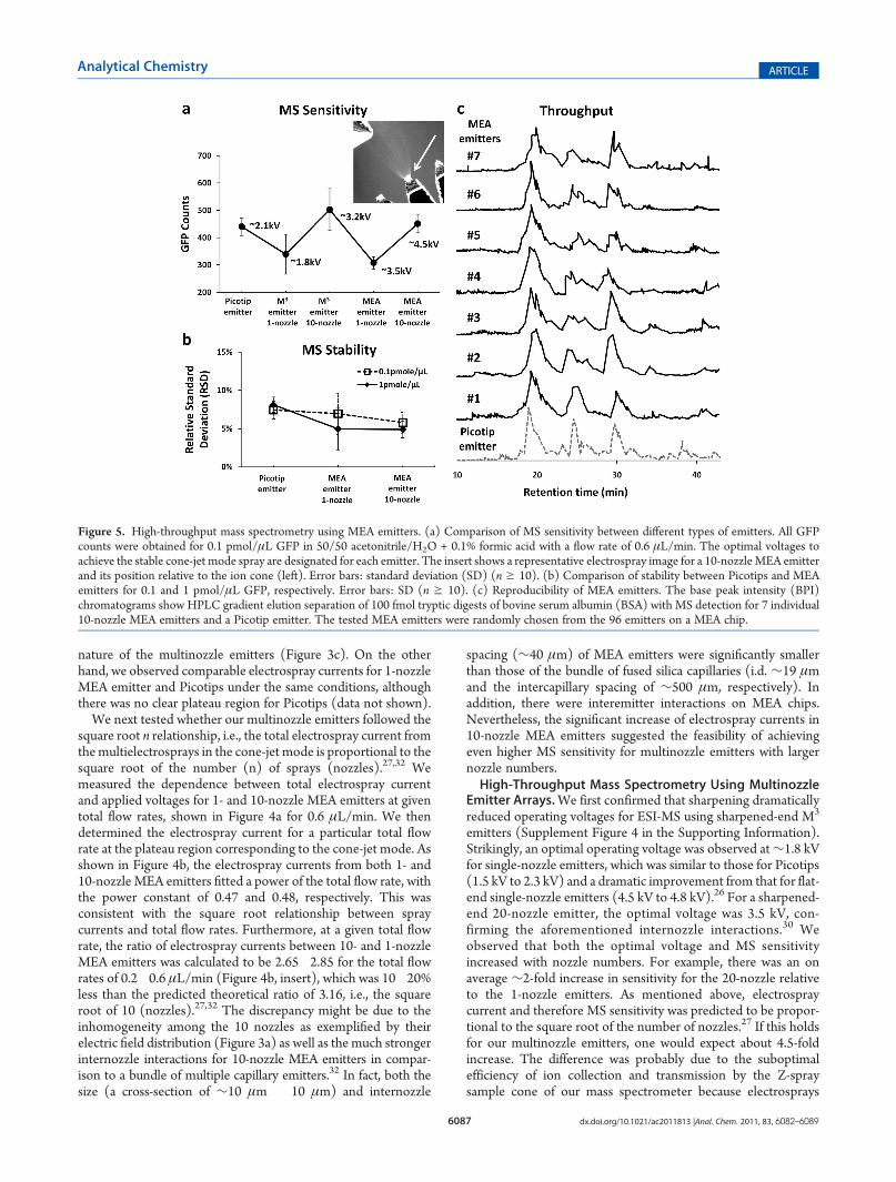
Emitter Arrays.We first confirmed that sharpening dramaticallyreduced operating voltages for ESI-MS using sharpened-end M3
emitters (Supplement Figure 4 in the Supporting Information).Strikingly, an optimal operating voltage was observed at∼1.8 kVfor single-nozzle emitters, which was similar to those for Picotips(1.5 kV to 2.3 kV) and a dramatic improvement from that for flat-end single-nozzle emitters (4.5 kV to 4.8 kV).26 For a sharpened-end 20-nozzle emitter, the optimal voltage was 3.5 kV, con-firming the aforementioned internozzle interactions.30 Weobserved that both the optimal voltage and MS sensitivityincreased with nozzle numbers. For example, there was an onaverage ∼2-fold increase in sensitivity for the 20-nozzle relativeto the 1-nozzle emitters. As mentioned above, electrospraycurrent and therefore MS sensitivity was predicted to be propor-tional to the square root of the number of nozzles.27 If this holdsfor our multinozzle emitters, one would expect about 4.5-foldincrease. The difference was probably due to the suboptimalefficiency of ion collection and transmission by the Z-spraysample cone of our mass spectrometer because electrosprays
Figure 5. High-throughput mass spectrometry using MEA emitters. (a) Comparison of MS sensitivity between different types of emitters. All GFPcounts were obtained for 0.1 pmol/μL GFP in 50/50 acetonitrile/H2O + 0.1% formic acid with a flow rate of 0.6 μL/min. The optimal voltages toachieve the stable cone-jet mode spray are designated for each emitter. The insert shows a representative electrospray image for a 10-nozzleMEA emitterand its position relative to the ion cone (left). Error bars: standard deviation (SD) (n g 10). (b) Comparison of stability between Picotips and MEAemitters for 0.1 and 1 pmol/μL GFP, respectively. Error bars: SD (n g 10). (c) Reproducibility of MEA emitters. The base peak intensity (BPI)chromatograms show HPLC gradient elution separation of 100 fmol tryptic digests of bovine serum albumin (BSA) with MS detection for 7 individual10-nozzle MEA emitters and a Picotip emitter. The tested MEA emitters were randomly chosen from the 96 emitters on a MEA chip.
6088 dx.doi.org/10.1021/ac2011813 |Anal. Chem. 2011, 83, 6082–6089
Analytical Chemistry ARTICLE
from multinozzle emitters were spread out significantly. Futureimplementation of a funnel-shaped sample cone20 may increaseMS sensitivity for multinozzle emitters.We next compared the performance of MEA emitters, free-
standing sharpened-end M3 emitters, and Picotips. All threetypes of emitters achieved comparably high MS sensitivity for0.1 μMGFP (Figure 5a). We observed a slightly (∼10%) higherMS sensitivity for both 10-nozzle MEA and M3 emitters thanPicotips. Importantly, both 10-nozzle MEA and M3 emittersachieved higher MS sensitivity than their 1-nozzle counterparts,validating the value of the multinozzle design. However, the foldchange was around 1.5�2.0 and less than what would be ex-pected from the square root n relationship, i.e.,∼3 fold, as shownby the electrospray current (Figure 4). As discussed above, futureoptimization of both the MS ion optics and the relative positionbetween MEA emitters and the ion cone (Figure 5a, insert) maymitigate this limitation. We achieved stable electrosprays at 3.5and 4.5 kV for 1- and 10-nozzle MEA emitters, respectively,while at 1.8 and 3.2 kV for 1- and 10-nozzle sharpened-end M3
emitters, respectively (Figure 5a). This was presumably due tothe emitter�emitter interactions on theMEA chip, in addition tothe nozzle�nozzle interactions within an emitter encountered byboth types of emitters. Therefore, an operating voltage higherthan the maximum of 5.0 kV provided by our current Q-TOFmass spectrometer is needed for MEA emitters with even largernozzle numbers (e.g., 40). We checked the MS stability forMEA emitters using 0.1 μM and 1.0 μM GFP, respectively. Therelative standard deviation (RSD) for either 1- or 10-nozzleMEAemitters was similar to that of Picotips (Figure 5b).We further demonstrated the proof-of-principle applications
of MEA emitters in high-throughput proteomics. Figure 5cshows representative LC�MS/MS chromatograms for 100 fmoltryptic digests of bovine serum albumin (BSA, ∼ 67 kDa), withone TOFMS (BPI, base peak intensity) each for one Picotip and7 individual MEA emitters chosen randomly out of the 96 on aMEA chip. There was no significant difference among thesechromatograms. In addition, BSA was confidently identified in allcases. With MEA emitters, we obtained on average a Mascotscore of 1300 and 43% sequence coverage with 27 peptidessequenced, while for Picotip emitters a Mascot score of 1333 and46% sequence coverage. The small discrepancy among MEAemitters presumably resulted from the slight difference in thepositioning of each emitter relative to the ion cone of our massspectrometer. This can be mitigated in the future through acomputer-controlled rotary system optimized for the 3 in.MEA chip.Our results demonstrated that MEA emitters could be inter-
faced with LC�MS/MS for sequential and reproducible high-sensitivity proteomic analyses. It is conceivable that multiple (upto 96) LC systems can be interfaced with our MEA chip toachieve, either sequential (if using only one mass spectrometer)or parallel (if using multiple, for example, miniaturized massspectrometers33,34), high-throughput MS analyses. More impor-tantly, our MEA platform is ready for the high-level integrationwith additional functional modules to achieve “lab-on-a-chip”.For example, the micropillar arrays embedded in the mainchannel can be utilized for digestion and separation. The fullyintegrated system will dramatically increase the sensitivity andthroughput for mass spectrometry-based metabolomics andproteomics, through efficient manipulation and processing ofan extremely small amount of samples (such as a single cell) andby diminishing the processing time for cell manipulation, and
protein digestion and separation, etc. Our platform can be furtherinterfaced with other technologies such as femtoliter and pico-liter-sized droplets for manipulating single cells.35 Since ourMEA chip is made of conductive Si, there is no liquid junctionand conductive coating needed to establish the electric contactbetween voltage supplies and the chip. This added advantagesimplifies the fluidic control on integrated MEA chips. Ourdesign can be extended to MEAs with even higher emitter num-bers (e.g., 384), thus enabling “ultrahigh-throughput”. Withfurther optimization, our MEA emitters will achieve even betterperformance in MS sensitivity and stability, thus enabling “ultra-high-sensitivity”.
’CONCLUSIONS
By taking advantage of the maturity and flexibility of siliconmicrofabrication technologies, we demonstrate massively parallelmultinozzle emitters integrated uniformly in a circular array,enabling high-sensitivity and high-throughput nanoelectrospraymass spectrometry. Our MEA chip is the first silicon-based,robust, and microfabricated monolithic multinozzle emittersimplemented in a high-throughput array format. Our MEA chiphas multiple advantages. First, it eliminates potential samplecarryover because each sample will be analyzed by a differentemitter. Second, it improves reproducibility for parallel analysisbecause emitters are identically microfabricated. Third, becauseof the robustness and inert nature of silicon material, the MEAchip can work under various conditions and be reused. Fourth,the clogging at the nozzle tips due to salt and debris buildup,typically encountered by the commercial Picotips, is significantmitigated due to the multinozzle design. In addition, a series ofprefilters can be readily fabricated in the main channels toprevent large debris or particles from entering the nozzles andthereby effectively reduce the clogging. Fifth, the throughput canbe further improved by increasing the wafer size (e.g., from 4 to6 in.) and optimizing the overall layout geometry. Lastly, the MSsensitivity can be further improved if emitters with an even largernumber of nozzles are interfaced with optimized ion optics forefficient ion collection and transmission. In summary, we presentthe first demonstration of silicon-based monolithic multinozzleemitter arrays (MEAs) for nanoelectrospray mass spectrometry.Once integrated with other functional modules, our MEA chipshave the potential to serve as a unified platform for futureultrahigh-sensitivity and ultrahigh-throughput proteomics andmetabolomics.
’ASSOCIATED CONTENT
bS Supporting Information. Additional information asnoted in text. This material is available free of charge via theInternet at http://pubs.acs.org.
’AUTHOR INFORMATION
Corresponding Author*Address: DaojingWang, Ph.D., Life Sciences Division, LawrenceBerkeley National Laboratory, 1 Cyclotron Road, MS 977,Berkeley, CA 94720. E-mail: [email protected]. Fax: 510-495-2535.
’ACKNOWLEDGMENT
P.M. and H.-T.W. contributed equally to this work. We thankDr. Woong Kim and Dr. Zhaoyu Zhang for technical assistance,
6089 dx.doi.org/10.1021/ac2011813 |Anal. Chem. 2011, 83, 6082–6089
Analytical Chemistry ARTICLE
Dr. Jian Jin for discussion, and UC-Berkeley Marvell Nanofabri-cation Laboratory for facility access. This work was supported bythe Director, Office of Science, of the U.S. Department of Energyunder Contract No. DE-AC02-05CH11231, and in part by theNational Institutes of Health Grant R21GM077870 (to D.W.).
’REFERENCES
(1) Wang, D.; Bodovitz, S. Trends Biotechnol. 2010, 28, 281–290.(2) Whittal, R. M.; Keller, B. O.; Li, L. Anal. Chem. 1998, 70, 5344–
5347.(3) Rubakhin, S. S.; Sweedler, J. V. Nat. Protoc. 2007, 2, 1987–1997.(4) Amantonico, A.; Urban, P. L.; Fagerer, S. R.; Balabin, R. M.;
Zenobi, R. Anal. Chem. 2010, 82, 7394–7400.(5) Lapainis, T.; Rubakhin, S. S.; Sweedler, J. V. Anal. Chem. 2009,
81, 5858–5864.(6) Shrestha, B.; Vertes, A. Anal. Chem. 2009, 81, 8265–8271.(7) Fenn, J. B.; Mann, M.; Meng, C. K.; Wong, S. F.; Whitehouse,
C. M. Science 1989, 246, 64–71.(8) Wilm, M.; Mann, M. Anal. Chem. 1996, 68, 1–8.(9) Whitesides, G. M. Nature 2006, 442, 368–373.(10) Sikanen, T.; Franssila, S.; Kauppila, T. J.; Kostiainen, R.;
Kotiaho, T.; Ketola, R. A. Mass Spectrom. Rev. 2010, 29, 351–391.(11) Licklider, L.; Wang, X. Q.; Desai, A.; Tai, Y. C.; Lee, T. D. Anal.
Chem. 2000, 72, 367–375.(12) Yang, Y.; Kameoka, J.; Wachs, T.; Henion, J. D.; Craighead,
H. G. Anal. Chem. 2004, 76, 2568–2574.(13) Kim, J. S.; Knapp, D. R. J. Am. Soc. Mass Spectrom. 2001,
12, 463–469.(14) Schilling, M.; Nigge, W.; Rudzinski, A.; Neyer, A.; Hergenroder,
R. Lab Chip 2004, 4, 220–224.(15) Le Gac, S.; Cren-Olive, C.; Rolando, C.; Arscott, S. J. Am. Soc.
Mass Spectrom. 2004, 15, 409–412.(16) Hoffmann, P.; Eschner,M.; Fritzsche, S.; Belder, D.Anal. Chem.
2009, 81, 7256–7261.(17) Mellors, J. S.; Jorabchi, K.; Smith, L. M.; Ramsey, J. M. Anal.
Chem. 2010, 82, 967–973.(18) Schultz, G. A.; Corso, T. N.; Prosser, S. J.; Zhang, S.Anal. Chem.
2000, 72, 4058–4063.(19) Gibson, G. T.;Mugo, S.M.; Oleschuk, R. D.Mass Spectrom. Rev.
2009, 28, 918–936.(20) Kelly, R. T.; Page, J. S.; Zhao, R.; Qian, W. J.; Mottaz, H. M.;
Tang, K.; Smith, R. D. Anal. Chem. 2008, 80, 143–149.(21) Su, S.; Gibson, G. T.; Mugo, S. M.; Marecak, D. M.; Oleschuk,
R. D. Anal. Chem. 2009, 81, 7281–7287.(22) Xue, Q.; Foret, F.; Dunayevskiy, Y. M.; Zavracky, P. M.;
McGruer, N. E.; Karger, B. L. Anal. Chem. 1997, 69, 426–430.(23) Liu, H.; Felten, C.; Xue, Q.; Zhang, B.; Jedrzejewski, P.; Karger,
B. L.; Foret, F. Anal. Chem. 2000, 72, 3303–3310.(24) Dayon, L.; Abonnenc, M.; Prudent, M.; Lion, N.; Girault, H. H.
J. Mass Spectrom. 2006, 41, 1484–1490.(25) Moini, M.; Jiang, L.; Bootwala, S. Rapid Commun. Mass Spectrom.
2011, 25, 789–794.(26) Kim, W.; Guo, M.; Yang, P.; Wang, D. Anal. Chem. 2007,
79, 3703–3707.(27) Tang, K.; Lin, Y.; Matson, D. W.; Kim, T.; Smith, R. D. Anal.
Chem. 2001, 73, 1658–1663.(28) Wang, D.; Park, J. S.; Chu, J. S.; Krakowski, A.; Luo, K.; Chen,
D. J.; Li, S. J. Biol. Chem. 2004, 279, 43725–43734.(29) Hosokawa, K.; Fujii, T.; Endo, I. Anal. Chem. 1999, 71, 4781–
4785.(30) Tatemoto, Y.; Ishikawa, R.; Takeuchi, M.; Takeshita, T.; Noda,
K.; Okazaki, T. Chem. Eng. Technol. 2007, 30, 1274–1279.(31) Marginean, I.; Kelly, R. T.; Page, J. S.; Tang, K.; Smith, R. D.
Anal. Chem. 2007, 79, 8030–8036.(32) Kelly, R. T.; Tang, K.; Irimia, D.; Toner, M.; Smith, R. D. Anal.
Chem. 2008, 80, 3824–3831.
(33) Gao, L.; Song, Q.; Patterson, G. E.; Cooks, R. G.; Ouyang, Z.Anal. Chem. 2006, 78, 5994–6002.
(34) Malcolm, A.; Wright, S.; Syms, R. R.; Dash, N.; Schwab, M. A.;Finlay, A. Anal. Chem. 2010, 82, 1751–1758.
(35) Chiu, D. T.; Lorenz, R. M. Acc. Chem. Res. 2009, 42, 649–658.