multiformat sdtv video decoder adv7181 - analog.com · multiformat sdtv video decoder adv7181 rev....
TRANSCRIPT
Multiformat SDTV Video Decoder ADV7181
Rev. B Information furnished by Analog Devices is believed to be accurate and reliable. However, no responsibility is assumed by Analog Devices for its use, nor for any infringements of patents or other rights of third parties that may result from its use. Specifications subject to change without notice. No license is granted by implication or otherwise under any patent or patent rights of Analog Devices. Trademarks and registered trademarks are the property of their respective owners.
One Technology Way, P.O. Box 9106, Norwood, MA 02062-9106, U.S.A. Tel: 781.329.4700 www.analog.com Fax: 781.461.3113 © 2005 Analog Devices, Inc. All rights reserved.
FEATURES Multiformat video decoder supports NTSC-(J, M, 4.43),
PAL-(B/D/G/H/I/M/N), SECAM Integrates three 54 MHz, 9-bit ADCs Clocked from a single 27 MHz crystal Line-locked clock-compatible (LLC) Adaptive Digital Line Length Tracking (ADLLT™) 5-line adaptive comb filters Proprietary architecture for locking to weak, noisy, and
unstable video sources such as VCRs and tuners Subcarrier frequency lock and status information output Integrated AGC with adaptive peak white mode Macrovision® copy protection detection CTI (chroma transient improvement) DNR (digital noise reduction) Multiple programmable analog input formats:
CVBS (composite video) S-Video (Y/C) YPrPb component (VESA, MII, SMPTE, and Betacam)
6 analog video input channels Automatic NTSC/PAL/SECAM identification Digital output formats (8-bit or16-bit):
ITU-R BT.656 YCrCb 4:2:2 output + HS, VS, and FIELD 0.5 V to 1.6 V analog signal input range Differential gain: 0.6% typ
Differential phase: 0.6° typ Programmable video controls:
Peak-white/hue/brightness/saturation/contrast Integrated on-chip video timing generator Free run mode (generates stable video ouput with no I/P) VBI decode support for
Close captioning, WSS, CGMS, EDTV, Gemstar® 1×/2× Power-down mode 2-wire serial MPU interface (I2C®-compatible) 3.3 V analog, 1.8 V digital core; 3.3 V IO supply Temperature grade: –40°C to +85°C 64-lead LQFP Pb-free package
APPLICATIONS DVD recorders PC video HDD-based PVRs/DVDRs LCD TVs Set-top boxes Security systems Digital televisions Portable video devices Automotive entertainment AVR receiver
GENERAL DESCRIPTION
The ADV7181 integrated video decoder automatically detects and converts a standard analog baseband television signal compatible with worldwide standards NTSC, PAL, and SECAM into 4:2:2 component video data compatible with 16-/8-bit CCIR601/CCIR656.
The advanced, highly flexible digital output interface enables performance video decoding and conversion in line-locked clock-based systems. This makes the device ideally suited for a broad range of applications with diverse analog video charac-teristics, including tape-based sources, broadcast sources, security/surveillance cameras, and professional systems.
The six analog input channels accept standard composite, S-Video, YPrPb video signals in an extensive number of combinations. AGC and clamp restore circuitry allow an input video signal peak-to-peak range of 0.5 V up to 1.6 V. Alternatively, these can be bypassed for manual settings.
The fixed 54 MHz clocking of the ADCs and datapath for all modes allow very precise, accurate sampling and digital filtering. The line-locked clock output allows the output data rate, timing signals, and output clock signals to be synchronous, asynchronous, or line locked even with ±5% line length variation. The output control signals allow glueless interface connections in almost any application. The ADV7181 modes are set up over a 2-wire, serial, bidirectional port (I2C-compatible).
The ADV7181 is fabricated in a 3.3 V CMOS process. Its monolithic CMOS construction ensures greater functionality with lower power dissipation.
The ADV7181 is packaged in a small 64-lead LFCSP and LQFP and Pb-free packages.
ADV7181
Rev. B | Page 2 of 104
TABLE OF CONTENTS Introduction ...................................................................................... 4
Analog Front End......................................................................... 4 Standard Definition Processor ................................................... 4
Functional Block Diagram .............................................................. 5 Specifications..................................................................................... 6
Electrical Characteristics............................................................. 6 Video Specifications..................................................................... 7 Timing Specifications .................................................................. 8 Analog Specifications .................................................................. 8 Thermal Specifications ................................................................ 8 Timing Diagrams ......................................................................... 9
Absolute Maximum Ratings.......................................................... 10 ESD Caution................................................................................ 10
Pin Configuration and Function Descriptions........................... 11 Analog Front End ........................................................................... 13
Analog Input Muxing ................................................................ 13 Global Control Registers ............................................................... 15
Power-Save Modes ..................................................................... 15 Reset Control .............................................................................. 15 Global Pin Control ..................................................................... 16
Global Status Registers................................................................... 18 Identification............................................................................... 18 Status 1 ......................................................................................... 18 Status 2 ......................................................................................... 19 Status 3 ......................................................................................... 19
Standard Definition Processor (SDP).......................................... 20 SD Luma Path ............................................................................. 20 SD Chroma Path......................................................................... 20 Sync Processing .......................................................................... 21 VBI Data Recovery..................................................................... 21 General Setup.............................................................................. 21 Color Controls ............................................................................ 24 Clamp Operation........................................................................ 26
Luma Filter .................................................................................. 27 Chroma Filter ............................................................................. 30 Gain Operation........................................................................... 31 Chroma Transient Improvement (CTI) .................................. 35 Digital Noise Reduction (DNR)............................................... 36 Comb Filters ............................................................................... 36 AV Code Insertion and Controls ............................................. 39 Synchronization Output Signals .............................................. 41 Sync Processing .......................................................................... 49 VBI Data Decode ....................................................................... 50
Pixel Port Configuration ............................................................... 61 MPU Port Description................................................................... 62
Register Accesses........................................................................ 63 Register Programming .............................................................. 63 I2C Sequencer.............................................................................. 63 I2C Control Register Map.......................................................... 64 I2C Register Map Details ........................................................... 67
I2C Programming Examples.......................................................... 93 Mode 1—CVBS Input (Composite Video on AIN6) ............ 93 Mode 2—S-Video Input (Y on AIN1 and C on AIN4)......... 94 Mode 3—525i/625i YPrPb Input (Y on AIN1, Pr on AIN3, and Pb on AIN5) ........................................................................ 94 Mode 4—CVBS Tuner Input CVBS PAL on AIN6 ............... 95
PCB Layout Recommendations.................................................... 96 Analog Interface Inputs............................................................. 96 Power Supply Decoupling ......................................................... 96 PLL ............................................................................................... 96 Digital Outputs (Both Data and Clocks) ................................ 96 Digital Inputs .............................................................................. 97 XTAL and Load Capacitor Value Selection ............................ 97
Typical Circuit Connection........................................................... 98 Outline Dimensions ..................................................................... 100
Ordering Guide ........................................................................ 101
ADV7181
Rev. B | Page 3 of 104
REVISION HISTORY
3/05—Rev. A to Rev. B
Changes to the Analog Specifications Section ..............................8 Changes to Table 20 and Table 21 ................................................17 Changes to Table 27 and Table 28 ................................................19 Change to Table 50..........................................................................25 Addition to the Clamp Operation Section...................................26 Changes to Figures 11.....................................................................29 Changes to Figures 12, 13, 14 ........................................................30 Changes to Chroma Filter Section................................................30 Deleted YPM Section and Renumbered Subsequent Tables .....30 Changes to Figure 15 ......................................................................31 Change to the Luma Gain Section ................................................32 Changes to Table 103 and Table 104............................................42 Deleted Table 172 and Renumbered Subsequent Tables............68 Changes to Table 176......................................................................71 Changes to Table 185......................................................................78 Changes to Table 192......................................................................83 Changes to Table 193......................................................................84 Changes to Table 194......................................................................85 Added XTAL and Load Capacitor Value Selection Section ......97 Change to Figure 41 ........................................................................98
7/04—Rev. 0 to Rev. A
Addition to Applications List ..........................................................1 Changes to Table 3 ............................................................................8 Changes to Table 5 ............................................................................8 Replaced Figure 3 ..............................................................................9 Changes to Global Pin Control Section .......................................16 Changes to Table 202 ......................................................................91 Changes to Table 203 ......................................................................92 Added package in Outline Dimensions Section .......................103 Changes to Ordering Guide.........................................................104
5/04—Revision 0: Initial Version
ADV7181
Rev. B | Page 4 of 104
INTRODUCTION The ADV7181 is a high quality, single chip, multiformat video decoder that automatically detects and converts PAL, NTSC, and SECAM standards in the form of composite, S-Video, and component video into a digital ITU-R BT.656 format.
The advanced, highly flexible digital output interface enables performance video decoding and conversion in line-locked clock-based systems. This makes the device ideally suited for a broad range of applications with diverse analog video charac-teristics, including tape-based sources, broadcast sources, security/surveillance cameras, and professional systems.
ANALOG FRONT END The ADV7181 analog front end comprises three 9-bit ADCs that digitize the analog video signal before applying it to the standard definition processor. The analog front end employs differential channels to each ADC to ensure high performance in mixed-signal applications.
The front end also includes a 6-channel input mux that enables multiple video signals to be applied to the ADV7181. Current and voltage clamps are positioned in front of each ADC to ensure that the video signal remains within the range of the converter. Fine clamping of the video signals is performed downstream by digital fine clamping within the ADV7181. The ADCs are configured to run in 4× oversampling mode.
STANDARD DEFINITION PROCESSOR The ADV7181 is capable of decoding a large selection of baseband video signals in composite, S-Video, and component formats. The video standards supported by the ADV7181 include PAL B/D/I/G/H, PAL60, PAL M, PAL N, PAL Nc, NTSC M/J, NTSC 4.43, and SECAM B/D/G/K/L. The ADV7181 can automatically detect the video standard and process it accordingly.
The ADV7181 has a 5-line, superadaptive, 2D comb filter that gives superior chrominance and luminance separation when decoding a composite video signal. This highly adaptive filter automatically adjusts its processing mode according to video standard and signal quality with no user intervention required. Video user controls such as brightness, contrast, saturation, and hue are also available within the ADV7181.
The ADV7181 implements a patented adaptive digital line-length tracking (ADLLT) algorithm to track varying video line lengths from sources such as a VCR. ADLLT enables the ADV7181 to track and decode poor quality video sources such as VCRs, noisy sources from tuner outputs, VCD players, and camcorders. The ADV7181 contains a chroma transient improvement (CTI) processor that sharpens the edge rate of chroma transitions, resulting in sharper vertical transitions.
The ADV7181 can process a variety of VBI data services such as closed captioning (CC), wide screen signaling (WSS), copy gen-eration management system (CGMS), EDTV, Gemstar 1×/2×, and extended data service (XDS). The ADV7181 is fully Macrovision certified; detection circuitry enables Type I, II, and III protection levels to be identified and reported to the user. The decoder is also fully robust to all Macrovision signal inputs.
ADV7181
Rev. B | Page 5 of 104
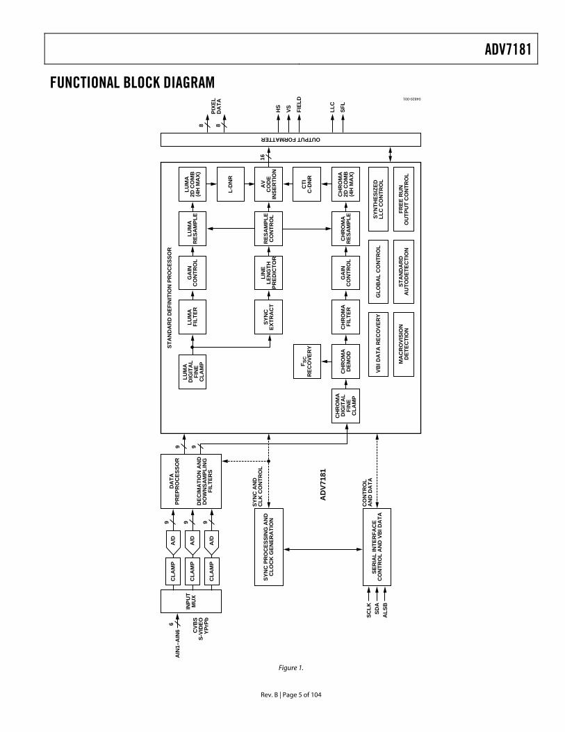
FUNCTIONAL BLOCK DIAGRAM
INPU
TM
UX
DA
TAPR
EPR
OC
ESSO
R
DEC
IMA
TIO
N A
ND
DO
WN
SAM
PLIN
GFI
LTER
S
STA
ND
AR
D D
EFIN
ITIO
N P
RO
CES
SOR
LUM
AFI
LTER
LUM
AD
IGIT
AL
FIN
EC
LAM
P
GA
INC
ON
TRO
LLU
MA
RES
AM
PLE
LUM
A2D
CO
MB
(4H
MA
X)
CH
RO
MA
FILT
ERC
HR
OM
AD
EMO
D
F SC
REC
OVE
RY
CH
RO
MA
DIG
ITA
LFI
NE
CLA
MP
GA
INC
ON
TRO
LC
HR
OM
AR
ESA
MPL
EC
HR
OM
A2D
CO
MB
(4H
MA
X)
L-D
NR
OUTPUT FORMATTER
SYN
CEX
TRA
CT
LIN
ELE
NG
THPR
EDIC
TOR
RES
AM
PLE
CO
NTR
OL
AV
CO
DE
INSE
RTI
ON
CTI
C-D
NR
A/D
CLA
MP
9
9 9A
/DC
LAM
P9
A/D
CLA
MP
9
VBI D
ATA
REC
OVE
RY
GLO
BA
L C
ON
TRO
LSY
NTH
ESIZ
EDLL
C C
ON
TRO
L
MA
CR
OVI
SIO
ND
ETEC
TIO
NST
AN
DA
RD
AU
TOD
ETEC
TIO
NFR
EE R
UN
OU
TPU
T C
ON
TRO
L
SYN
C P
RO
CES
SIN
G A
ND
CLO
CK
GEN
ERA
TIO
N
SER
IAL
INTE
RFA
CE
CO
NTR
OL
AN
D V
BI D
ATA
SCLK
AIN
1–A
IN6
SDA
ALS
B
AD
V718
1
CO
NTR
OL
AN
D D
ATA
SYN
C A
ND
CLK
CO
NTR
OL
16
HS
88
PIXE
LD
ATA
VS FIEL
D
LLC
SFL
CVB
SS-
VID
EOYP
rPb
6
04820-001
Figure 1.
ADV7181
Rev. B | Page 6 of 104
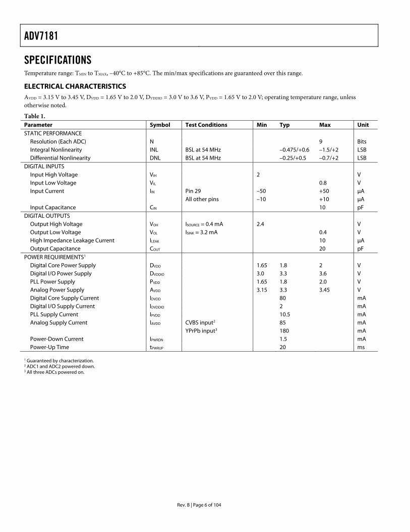
SPECIFICATIONS Temperature range: TMIN to TMAX, –40°C to +85°C. The min/max specifications are guaranteed over this range.
ELECTRICAL CHARACTERISTICS AVDD = 3.15 V to 3.45 V, DVDD = 1.65 V to 2.0 V, DVDDIO = 3.0 V to 3.6 V, PVDD = 1.65 V to 2.0 V; operating temperature range, unless otherwise noted.
Table 1. Parameter Symbol Test Conditions Min Typ Max Unit STATIC PERFORMANCE
Resolution (Each ADC) N 9 Bits Integral Nonlinearity INL BSL at 54 MHz –0.475/+0.6 –1.5/+2 LSB Differential Nonlinearity DNL BSL at 54 MHz –0.25/+0.5 –0.7/+2 LSB
DIGITAL INPUTS Input High Voltage VIH 2 V Input Low Voltage VIL 0.8 V Input Current IIN Pin 29 –50 +50 µA All other pins –10 +10 µA Input Capacitance CIN 10 pF
DIGITAL OUTPUTS Output High Voltage VOH ISOURCE = 0.4 mA 2.4 V Output Low Voltage VOL ISINK = 3.2 mA 0.4 V High Impedance Leakage Current ILEAK 10 µA Output Capacitance COUT 20 pF
POWER REQUIREMENTS1 Digital Core Power Supply DVDD 1.65 1.8 2 V Digital I/O Power Supply DVDDIO 3.0 3.3 3.6 V PLL Power Supply PVDD 1.65 1.8 2.0 V Analog Power Supply AVDD 3.15 3.3 3.45 V Digital Core Supply Current IDVDD 80 mA Digital I/O Supply Current IDVDDIO 2 mA PLL Supply Current IPVDD 10.5 mA Analog Supply Current IAVDD CVBS input2 85 mA YPrPb input3 180 mA Power-Down Current IPWRDN 1.5 mA Power-Up Time tPWRUP 20 ms
1 Guaranteed by characterization. 2 ADC1 and ADC2 powered down. 3 All three ADCs powered on.
ADV7181
Rev. B | Page 7 of 104
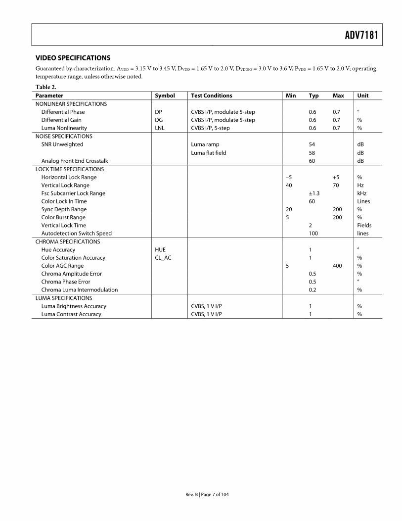
VIDEO SPECIFICATIONS Guaranteed by characterization. AVDD = 3.15 V to 3.45 V, DVDD = 1.65 V to 2.0 V, DVDDIO = 3.0 V to 3.6 V, PVDD = 1.65 V to 2.0 V; operating temperature range, unless otherwise noted.
Table 2. Parameter Symbol Test Conditions Min Typ Max Unit NONLINEAR SPECIFICATIONS
Differential Phase DP CVBS I/P, modulate 5-step 0.6 0.7 ° Differential Gain DG CVBS I/P, modulate 5-step 0.6 0.7 % Luma Nonlinearity LNL CVBS I/P, 5-step 0.6 0.7 %
NOISE SPECIFICATIONS SNR Unweighted Luma ramp 54 dB
Luma flat field 58 dB Analog Front End Crosstalk 60 dB
LOCK TIME SPECIFICATIONS Horizontal Lock Range –5 +5 % Vertical Lock Range 40 70 Hz Fsc Subcarrier Lock Range ±1.3 kHz Color Lock In Time 60 Lines Sync Depth Range 20 200 % Color Burst Range 5 200 % Vertical Lock Time 2 Fields Autodetection Switch Speed 100 lines
CHROMA SPECIFICATIONS Hue Accuracy HUE 1 ° Color Saturation Accuracy CL_AC 1 % Color AGC Range 5 400 % Chroma Amplitude Error 0.5 % Chroma Phase Error 0.5 ° Chroma Luma Intermodulation 0.2 %
LUMA SPECIFICATIONS Luma Brightness Accuracy CVBS, 1 V I/P 1 % Luma Contrast Accuracy CVBS, 1 V I/P 1 %
ADV7181
Rev. B | Page 8 of 104
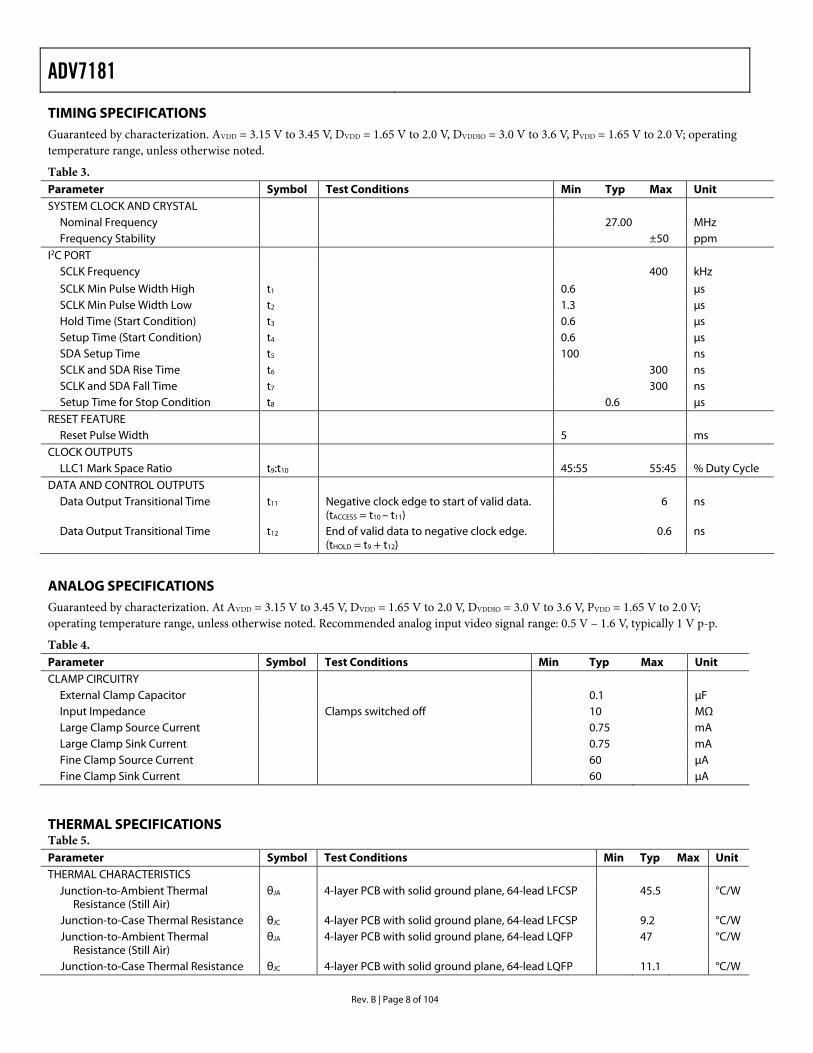
TIMING SPECIFICATIONS Guaranteed by characterization. AVDD = 3.15 V to 3.45 V, DVDD = 1.65 V to 2.0 V, DVDDIO = 3.0 V to 3.6 V, PVDD = 1.65 V to 2.0 V; operating temperature range, unless otherwise noted.
Table 3. Parameter Symbol Test Conditions Min Typ Max Unit SYSTEM CLOCK AND CRYSTAL
Nominal Frequency 27.00 MHz Frequency Stability ±50 ppm
I2C PORT SCLK Frequency 400 kHz
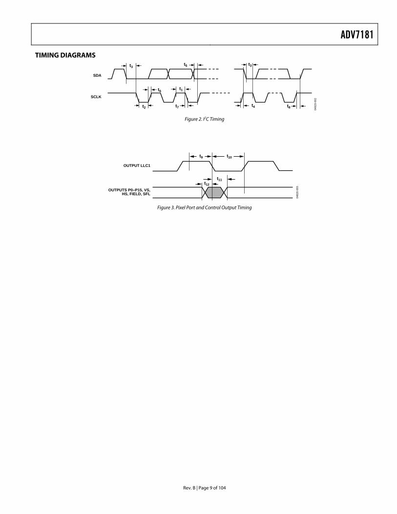
SCLK Min Pulse Width High t1 0.6 µs SCLK Min Pulse Width Low t2 1.3 µs Hold Time (Start Condition) t3 0.6 µs Setup Time (Start Condition) t4 0.6 µs SDA Setup Time t5 100 ns SCLK and SDA Rise Time t6 300 ns SCLK and SDA Fall Time t7 300 ns Setup Time for Stop Condition t8 0.6 µs
RESET FEATURE Reset Pulse Width 5 ms
CLOCK OUTPUTS LLC1 Mark Space Ratio t9:t10 45:55 55:45 % Duty Cycle
DATA AND CONTROL OUTPUTS Data Output Transitional Time t11 Negative clock edge to start of valid data.
(tACCESS = t10 – t11) 6 ns
Data Output Transitional Time t12 End of valid data to negative clock edge. (tHOLD = t9 + t12)
0.6 ns
ANALOG SPECIFICATIONS Guaranteed by characterization. At AVDD = 3.15 V to 3.45 V, DVDD = 1.65 V to 2.0 V, DVDDIO = 3.0 V to 3.6 V, PVDD = 1.65 V to 2.0 V; operating temperature range, unless otherwise noted. Recommended analog input video signal range: 0.5 V – 1.6 V, typically 1 V p-p.
Table 4. Parameter Symbol Test Conditions Min Typ Max Unit CLAMP CIRCUITRY
External Clamp Capacitor 0.1 µF Input Impedance Clamps switched off 10 MΩ Large Clamp Source Current 0.75 mA Large Clamp Sink Current 0.75 mA Fine Clamp Source Current 60 µA Fine Clamp Sink Current 60 µA
THERMAL SPECIFICATIONS Table 5. Parameter Symbol Test Conditions Min Typ Max Unit THERMAL CHARACTERISTICS
Junction-to-Ambient Thermal Resistance (Still Air)
θJA 4-layer PCB with solid ground plane, 64-lead LFCSP 45.5 °C/W
Junction-to-Case Thermal Resistance θJC 4-layer PCB with solid ground plane, 64-lead LFCSP 9.2 °C/W Junction-to-Ambient Thermal
Resistance (Still Air) θJA 4-layer PCB with solid ground plane, 64-lead LQFP 47 °C/W
Junction-to-Case Thermal Resistance θJC 4-layer PCB with solid ground plane, 64-lead LQFP 11.1 °C/W
ADV7181
Rev. B | Page 9 of 104
TIMING DIAGRAMS
0482
0-00
2
SDA
SCLK
t3 t5 t3
t4 t8
t6
t7t2
t1
Figure 2. I2C Timing
OUTPUT LLC1
0482
0-00
3
OUTPUTS P0–P15, VS,HS, FIELD, SFL
t9 t10
t11t12
Figure 3. Pixel Port and Control Output Timing
ADV7181
Rev. B | Page 10 of 104
ABSOLUTE MAXIMUM RATINGS
Table 6. Parameter Rating AVDD to GND 4 V AVDD to AGND 4 V DVDD to DGND 2.2 V PVDD to AGND 2.2 V DVDDIO to DGND 4 V DVDDIO to AVDD –0.3 V to +0.3 V PVDD to DVDD –0.3 V to +0.3 V DVDDIO – PVDD –0.3 V to +2 V DVDDIO – DVDD –0.3 V to +2 V AVDD – PVDD –0.3 V to +2 V AVDD – DVDD –0.3 V to +2 V Digital Inputs Voltage to DGND –0.3 V to DVDDIO + 0.3 V Digital Output Voltage to DGND –0.3 V to DVDDIO + 0.3 V Analog Inputs to AGND AGND – 0.3 V to AVDD + 0.3 V Maximum Junction Temperature
(TJ max) 150°C
Storage Temperature Range –65°C to +150°C Infrared Reflow Soldering (20 s) 260°C
Stresses above those listed under Absolute Maximum Ratings may cause permanent damage to the device. This is a stress rating only; functional operation of the device at these or any other conditions above those indicated in the operational sections of this specification is not implied. Exposure to absolute maximum rating conditions for extended periods may affect device reliability.
ESD CAUTION ESD (electrostatic discharge) sensitive device. Electrostatic charges as high as 4000 V readily accumulate on the human body and test equipment and can discharge without detection. Although this product features proprietary ESD protection circuitry, permanent damage may occur on devices subjected to high energy electrostatic discharges. Therefore, proper ESD precautions are recommended to avoid performance degradation or loss of functionality.
ADV7181
Rev. B | Page 11 of 104
PIN CONFIGURATION AND FUNCTION DESCRIPTIONS
NC 1
HS 2
DGND 3
DVDDIO 4
P11 5
P10 6
P9 7
P8 8
SFL 9
DGND 10
DVDDIO 11
NC 12
NC 13
P7 14
P6 15
P5 16
AIN548
AIN447
AIN346
AGND45
CAPC244
AGND43
CML42
REFOUT41
AVDD40
CAPY239
CAPY138
AGND37
AIN236
AIN135
DGND34
NC33
P4
17
P3
18
P2
19
LLC
20
XTA
L1
21
XTA
L
22
DVD
D
23
DG
ND
24P1
25P0
26
NC
27
NC
28
PWR
DN
29
ELPF
30
PVD
D
31
AG
ND
32
VS
64
FIEL
D
63
P12
62
P13
61
P14
60
P15
59
DVD
D
58
DG
ND
57
NC
56
NC
55
SCLK
54
SDA
TA
53
ALS
B
52
RES
ET
51
NC
50
AIN
6
49
ADV7181TOP VIEW
(Not to Scale)
NC = NO CONNECT 0482
0-00
4
PIN 1INDICATOR
Figure 4. 64-Lead LFCSP/LQFP Pin Configuration
Table 7. Pin Function Descriptions Pin No. Mnemonic Type Function 3, 10, 24, 34, 57 DGND G Digital Ground. 32, 37, 43, 45 AGND G Analog Ground. 4, 11 DVDDIO P Digital I/O Supply Voltage (3.3 V). 23, 58 DVDD P Digital Core Supply Voltage (1.8 V). 40 AVDD P Analog Supply Voltage (3.3 V). 31 PVDD P PLL Supply Voltage (1.8 V). 35, 36, 46–49 AIN1–AIN6 I Analog Video Input Channels. 1, 12, 13, 27, 28, 33, 50, 55, 56
NC No Connect Pins.
26, 25, 19, 18, 17, 16, 15, 14, 8, 7, 6, 5, 62, 61, 60, 59
P0–P15 O Video Pixel Output Port.
2 HS O Horizontal Synchronization Output Signal. 64 VS O Vertical Synchronization Output Signal. 63 FIELD O Field Synchronization Output Signal. 53 SDA I/O I2C Port Serial Data Input/Output Pin. 54 SCLK I I2C Port Serial Clock Input (Max Clock Rate of 400 kHz). 52 ALSB I This pin selects the I2C address for the ADV7181. ALSB set to a Logic 0 sets the address for a
write as 0x40; for ALSB set to a logic high, the address selected is 0x42. 51 RESET I System Reset Input, Active Low. A minimum low reset pulse width of 5 ms is required to
reset the ADV7181 circuitry. 20 LLC O This is a line-locked output clock for the pixel data output by the ADV7181. Nominally
27 MHz, but varies up or down according to video line length. 22 XTAL I This is the input pin for the 27 MHz crystal, or can be overdriven by an external 3.3 V,
27 MHz clock oscillator source. In crystal mode, the crystal must be a fundamental crystal.
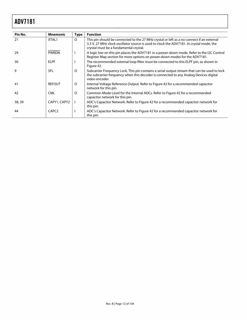
ADV7181
Rev. B | Page 12 of 104
Pin No. Mnemonic Type Function 21 XTAL1 O This pin should be connected to the 27 MHz crystal or left as a no connect if an external
3.3 V, 27 MHz clock oscillator source is used to clock the ADV7181. In crystal mode, the crystal must be a fundamental crystal.
29 PWRDN I A logic low on this pin places the ADV7181 in a power-down mode. Refer to the I2C Control Register Map section for more options on power-down modes for the ADV7181.
30 ELPF I The recommended external loop filter must be connected to this ELPF pin, as shown in Figure 42.
9 SFL O Subcarrier Frequency Lock. This pin contains a serial output stream that can be used to lock the subcarrier frequency when this decoder is connected to any Analog Devices digital video encoder.
41 REFOUT O Internal Voltage Reference Output. Refer to Figure 42 for a recommended capacitor network for this pin.
42 CML O Common-Mode Level for the Internal ADCs. Refer to Figure 42 for a recommended capacitor network for this pin.
38, 39 CAPY1, CAPY2 I ADC’s Capacitor Network. Refer to Figure 42 for a recommended capacitor network for this pin.
44 CAPC2 I ADC’s Capacitor Network. Refer to Figure 42 for a recommended capacitor network for this pin.
ADV7181
Rev. B | Page 13 of 104
ANALOG FRONT END
0482
0-00
5
AIN2AIN1AIN4AIN3AIN6AIN5
AIN
5A
IN6
AIN
3A
IN4
AIN
1A
IN2
AIN4AIN3AIN6AIN5
AIN6AIN5
ADC_SW_MAN_EN
ADC0_SW[3:0]
ADC1_SW[3:0]
ADC0_SW[3:0]
ADC2
ADC1
ADC0
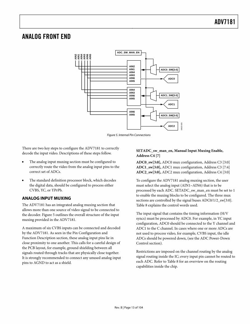
Figure 5. Internal Pin Connections
There are two key steps to configure the ADV7181 to correctly decode the input video. Descriptions of these steps follow.
• The analog input muxing section must be configured to correctly route the video from the analog input pins to the correct set of ADCs.
• The standard definition processor block, which decodes the digital data, should be configured to process either CVBS, YC, or YPrPb.
ANALOG INPUT MUXING The ADV7181 has an integrated analog muxing section that allows more than one source of video signal to be connected to the decoder. Figure 5 outlines the overall structure of the input muxing provided in the ADV7181.
A maximum of six CVBS inputs can be connected and decoded by the ADV7181. As seen in the Pin Configuration and Function Description section, these analog input pins lie in close proximity to one another. This calls for a careful design of the PCB layout, for example, ground shielding between all signals routed through tracks that are physically close together. It is strongly recommended to connect any unused analog input pins to AGND to act as a shield.
SETADC_sw_man_en, Manual Input Muxing Enable, Address C4 [7]
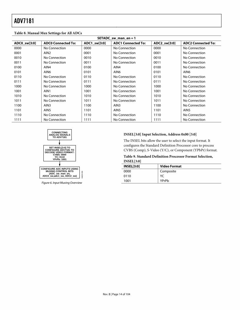
ADC0_sw[3:0], ADC0 mux configuration, Address C3 [3:0] ADC1_sw[3:0], ADC1 mux configuration, Address C3 [7:4] ADC2_sw[3:0], ADC2 mux configuration, Address C4 [3:0]
To configure the ADV7181 analog muxing section, the user must select the analog input (AIN1–AIN6) that is to be processed by each ADC. SETADC_sw_man_en must be set to 1 to enable the muxing blocks to be configured. The three mux sections are controlled by the signal buses ADC0/1/2_sw[3:0]. Table 8 explains the control words used.
The input signal that contains the timing information (H/V syncs) must be processed by ADC0. For example, in YC input configuration, ADC0 should be connected to the Y channel and ADC1 to the C channel. In cases where one or more ADCs are not used to process video, for example, CVBS input, the idle ADCs should be powered down, (see the ADC Power-Down Control section).
Restrictions are imposed on the channel routing by the analog signal routing inside the IC; every input pin cannot be routed to each ADC. Refer to Table 8 for an overview on the routing capabilities inside the chip.
ADV7181
Rev. B | Page 14 of 104
Table 8. Manual Mux Settings for All ADCs SETADC_sw_man_en = 1
ADC0_sw[3:0] ADC0 Connected To: ADC1_sw[3:0] ADC1 Connected To: ADC2_sw[3:0] ADC2 Connected To: 0000 No Connection 0000 No Connection 0000 No Connection 0001 AIN2 0001 No Connection 0001 No Connection 0010 No Connection 0010 No Connection 0010 No Connection 0011 No Connection 0011 No Connection 0011 No Connection 0100 AIN4 0100 AIN4 0100 No Connection 0101 AIN6 0101 AIN6 0101 AIN6 0110 No Connection 0110 No Connection 0110 No Connection 0111 No Connection 0111 No Connection 0111 No Connection 1000 No Connection 1000 No Connection 1000 No Connection 1001 AIN1 1001 No Connection 1001 No Connection 1010 No Connection 1010 No Connection 1010 No Connection 1011 No Connection 1011 No Connection 1011 No Connection 1100 AIN3 1100 AIN3 1100 No Connection 1101 AIN5 1101 AIN5 1101 AIN5 1110 No Connection 1110 No Connection 1110 No Connection 1111 No Connection 1111 No Connection 1111 No Connection
0482
0-00
6
CONNECTINGANALOG SIGNALS
TO ADV7181
SET INSEL[3:0] TOCONFIGURE ADV7181 TODECODE VIDEO FORMAT:
CVBS: 0000YC: 0110
YPrPb: 1001
CONFIGURE ADC INPUTS USINGMUXING CONTROL BITS
(ADC_sw_man_en,ADC0_sw,adc1_sw, ADC2_sw)
Figure 6. Input Muxing Overview
INSEL[3:0] Input Selection, Address 0x00 [3:0]
The INSEL bits allow the user to select the input format. It configures the Standard Definition Processor core to process CVBS (Comp), S-Video (Y/C), or Component (YPbPr) format.
Table 9. Standard Definition Processor Format Selection, INSEL[3:0] INSEL[3:0] Video Format 0000 Composite 0110 YC 1001 YPrPb
ADV7181
Rev. B | Page 15 of 104
GLOBAL CONTROL REGISTERS Register control bits listed in this section affect the whole chip.
POWER-SAVE MODES Power-Down
PDBP, Address 0x0F [2]
There are two ways to shut down the digital core of the ADV7181: a pin (PWRDN) and a bit (PWRDN see below). The PDBP controls which of the two has the higher priority. The default is to give the pin (PWRDN) priority. This allows the user to have the ADV7181 powered down by default.
Table 10. PDBP Function PDBP Description 0 (default) Digital core power controlled by the PWRDN pin
(bit is disregarded). 1 Bit has priority (pin is disregarded).
PWRDN, Address 0x0F [5]
Setting the PWRDN bit switches the ADV7181 into a chip-wide power-down mode. The power-down stops the clock from entering the digital section of the chip, thereby freezing its operation. No I2C bits are lost during power-down. The PWRDN bit also affects the analog blocks and switches them into low current modes. The I2C interface itself is unaffected, and remains operational in power-down mode.
The ADV7181 leaves the power-down state if the PWRDN bit is set to 0 (via I2C), or if the overall part is reset using the RESET pin.
PDBP must be set to 1 for the PWRDN bit to power down the ADV7181.
Table 11. PWRDN Function PWRDN Description 0 (default) Chip operational. 1 ADV7181 in chip-wide power-down.
ADC Power-Down Control
The ADV7181 contains three 9-bit ADCs (ADC 0, ADC 1, and ADC 2). If required, it is possible to power down each ADC individually.
When should the ADCs be powered down?
• CVBS mode. ADC 1 and ADC 2 should be powered down to save on power consumption.
• S-Video mode. ADC 2 should be powered down to save on power consumption.
PWRDN_ADC_0, Address 0x3A [3] Table 12. PWRDN_ADC_0 Function PWRDN_ADC_0 Description 0 (default) ADC normal operation. 1 Power down ADC 0.
PWRDN_ADC_1, Address 0x3A [2] Table 13. PWRDN_ADC_1 Function PWRDN_ADC_1 Description 0 (default) ADC normal operation. 1 Power down ADC 1.
PWRDN_ADC_2, Address 0x3A [1] Table 14. PWRDN_ADC_2 Function PWRDN_ADC_2 Description 0 (default) ADC normal operation. 1 Power down ADC 2.
RESET CONTROL
Chip Reset (RES), Address 0x0F [7]
Setting this bit, equivalent to controlling the RESET pin on the ADV7181, issues a full chip reset. All I2C registers are reset to their default values. (Some register bits do not have a reset value specified. They keep their last written value. Those bits are marked as having a reset value of x in the register table.) After the reset sequence, the part immediately starts to acquire the incoming video signal.
Notes
• After setting the RES bit (or initiating a reset via the pin), the part returns to the default mode of operation with respect to its primary mode of operation. All I2C bits are loaded with their default values, making this bit self-clearing.
• Executing a software reset takes approximately 2 ms. However, it is recommended to wait 5 ms before further I2C writes are performed.
• The I2C master controller receives a no acknowledge condition on the ninth clock cycle when chip reset is implemented. See the MPU Port Description section.
Table 15. RES Function RES Description 0 (default) Normal operation. 1 Start reset sequence.
ADV7181
Rev. B | Page 16 of 104
GLOBAL PIN CONTROL Three-State Output Drivers
TOD, Address 0x03 [6]
This bit allows the user to three-state the output drivers of the ADV7181.
Upon setting the TOD bit, the P15–P0, HS, VS, FIELD, and SFL pins are three-stated.
The timing pins (HS/VS/FIELD) can be forced active via the TIM_OE bit. For more information on three-state control, refer to the following sections:
• Three-State LLC Driver
• Timing Signals Output Enable
Individual drive strength controls are provided via the DR_STR_XX bits. Table 16. TOD Function TOD Description 0 (default) Output drivers enabled. 1 Output drivers three-stated.
Three-State LLC Driver
TRI_LLC, Address 0x0E [6]
This bit allows the output drivers for the LLC pin of the ADV7181 to be three-stated. For more information on three-state control, refer to the following sections:
• Three-State Output Drivers
• Timing Signals Output Enable
Individual drive strength controls are provided via the DR_STR_XX bits.
Table 17. TRI_LLC Function TRI_LLC Description 0 (default) LLC pin drivers working according to the
DR_STR_C[1:0] setting (pin enabled). 1 LLC pin drivers three-stated.
Timing Signals Output Enable
TIM_OE, Address 0x04 [3]
The TIM_OE bit should be regarded as an addition to the TOD bit. Setting it high forces the output drivers for HS, VS, and FIELD into the active (that is, driving) state even if the TOD bit is set. If set to low, the HS, VS, and FIELD pins are three-stated depending on the TOD bit. This functionality is useful if the decoder is to be used as a timing generator only. This may be the case if only the timing signals are to be extracted from an incoming signal, or if the part is in free-run mode where a separate chip can output, for instance, a company logo.
For more information on three-state control, refer to the following sections:
• Three-State Output Drivers
• Three-State LLC Driver
Individual drive strength controls are provided via the DR_STR_XX bits.
Table 18. TIM_OE Function TIM_OE Description 0 (default) HS, VS, FIELD three-stated according to the
TOD bit. 1 HS, VS, FIELD are forced active all the time. The
DR_STR_S[1:0] setting determines drive strength.
Drive Strength Selection (Data)
DR_STR[1:0] Address 0x04 [5:4]
For EMC and crosstalk reasons, it may be desirable to strengthen or weaken the drive strength of the output drivers. The DR_STR[1:0] bits affect the P[15:0] output drivers.
For more information on three-state control, refer to the following sections:
• Drive Strength Selection (Clock)
• Drive Strength Selection (Sync)
Table 19. DR_STR Function DR_STR[1:0] Description 00 Low drive strength (1×). 01 (default) Medium low drive strength (2×). 10 Medium high drive strength (3×). 11 High drive strength (4×).
ADV7181
Rev. B | Page 17 of 104
Drive Strength Selection (Clock)
DR_STR_C[1:0] Address 0x0E [3:2]
The DR_STR_C[1:0] bits can be used to select the strength of the clock signal output driver (LLC pin). For more information, refer to the following sections:
• Drive Strength Selection (Sync)
• Drive Strength Selection (Data)
Table 20. DR_STR_C Function DR_STR_C[1:0] Description 00 Low drive strength (1×). 01 (default) Medium low drive strength (2×). 10 Medium high drive strength (3×). 11 High drive strength (4×).
Drive Strength Selection (Sync)
DR_STR_S[1:0] Address 0x0E [1:0]
The DR_STR_S[1:0] bits allow the user to select the strength of the synchronization signals with which HS, VS, and F are driven. For more information, refer to the following sections:
• Drive Strength Selection (Clock)
• Drive Strength Selection (Data)
Table 21. DR_STR_S Function DR_STR_S[1:0] Description 00 Low drive strength (1×). 01 (default) Medium low drive strength (2×). 10 Medium high drive strength (3×). 11 High drive strength (4×).
Enable Subcarrier Frequency Lock Pin
EN_SFL_PIN Address 0x04 [1]
The EN_SFL_PIN bit enables the output of subcarrier lock information (also known as GenLock) from the ADV7181 to an encoder in a decoder-encoder back-to-back arrangement.
Table 22. EN_SFL_PIN EN_SFL_PIN Description 0 (default) Subcarrier frequency lock output is disabled. 1 Subcarrier frequency lock information is
presented on the SFL pin.
Polarity LLC Pin
PCLK Address 0x37 [0]
The polarity of the clock that leaves the ADV7181 via the LLC pin can be inverted using the PCLK bit.
Changing the polarity of the LLC clock output may be necessary to meet the setup-and-hold time expectations of follow-on chips.
Table 23. PCLK Function PCLK Description 0 Invert LLC output polarity. 1 (default) LLC output polarity normal (as per the Timing
Diagrams).
ADV7181
Rev. B | Page 18 of 104
GLOBAL STATUS REGISTERS Four registers provide summary information about the video decoder. The IDENT register allows the user to identify the revision code of the ADV7181. The other three registers contain status bits from the ADV7181.
IDENTIFICATION
IDENT[7:0] Address 0x11 [7:0]
Provides identification of the revision of the ADV7181. Review the list of IDENT code readback values for the various versions shown in Table 24.
Table 24. IDENT Function IDENT[7:0] Description 0x0D ADV7181-ES1 0x0E ADV7181-ES2 0x0F or 0x10 ADV7181-FT 0x11 ADV7181 (Version 2)
STATUS 1
STATUS_1[7:0] Address 0x10 [7:0]
This read-only register provides information about the internal status of the ADV7181.
See CIL[2:0] Count Into Lock, Address 0x51 [2:0] and COL[2:0] Count Out of Lock, Address 0x51 [5:3] for information on the timing.
Depending on the setting of the FSCLE bit, the Status[0] and Status[1] are based solely on horizontal timing info or on the horizontal timing and lock status of the color subcarrier. See the FSCLE Fsc Lock Enable, Address 0x51 [7] section.
Autodetection Result
AD_RESULT[2:0] Address 0x10 [6:4]
The AD_RESULT[2:0] bits report back on the findings from the autodetection block. Consult the General Setup sec-tion for more information on enabling the autodetection block, and the Autodetection of SD Modes section to find out how to configure it.
Table 25. AD_RESULT Function AD_RESULT[2:0] Description 000 NTSM-MJ 001 NTSC-443 010 PAL-M 011 PAL-60 100 PAL-BGHID 101 SECAM 110 PAL-Combination N 111 SECAM 525
Table 26. STATUS 1 Function STATUS 1 [7:0] Bit Name Description 0 IN_LOCK In lock (right now). 1 LOST_LOCK Lost lock (since last read of this register). 2 FSC_LOCK Fsc locked (right now). 3 FOLLOW_PW AGC follows peak white algorithm. 4 AD_RESULT.0 Result of autodetection. 5 AD_RESULT.1 Result of autodetection. 6 AD_RESULT.2 Result of autodetection. 7 COL_KILL Color kill active.
ADV7181
Rev. B | Page 19 of 104
STATUS 2
STATUS_2[7:0], Address 0x12 [7:0] Table 27. STATUS 2 Function STATUS 2 [7:0] Bit Name Description 0 MVCS DET Detected Macrovision color striping. 1 MVCS T3 Macrovision color striping protection. Conforms to Type 3 (if high), and Type 2 (if low). 2 MV_PS DET Detected Macrovision pseudo sync pulses. 3 MV_AGC DET Detected Macrovision AGC pulses. 4 LL_NSTD Line length is nonstandard. 5 FSC_NSTD Fsc frequency is nonstandard. 6 Reserved 7 Reserved
STATUS 3
STATUS_3[7:0], Address 0x13 [7:0] Table 28. STATUS 3 Function STATUS 3 [7:0] Bit Name Description 0 INST_HLOCK Horizontal lock indicator (instantaneous). 1 Reserved 2 Reserved 3 Reserved 4 FREE_RUN_ACT ADV7181 outputs a blue screen (see the DEF_VAL_AUTO_EN Default Value Automatic
Enable, Address 0x0C [1] section). 5 STD_FLD_LEN Field length is correct for currently selected video standard. 6 INTERLACED Interlaced video detected (field sequence found). 7 PAL_SW_LOCK Reliable sequence of swinging bursts detected.
ADV7181
Rev. B | Page 20 of 104
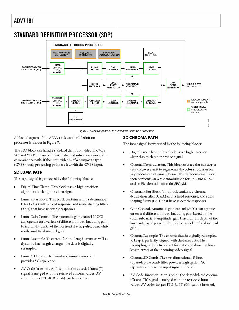
STANDARD DEFINITION PROCESSOR (SDP)
0482
0-00
7
DIGITIZED CVBSDIGITIZED Y (YC)
VIDEO DATAOUTPUT
STANDARD DEFINITION PROCESSOR
DIGITIZED CVBSDIGITIZED C (YC)
MACROVISIONDETECTION
VBI DATARECOVERY
STANDARDAUTODETECTION
LUMAFILTER
LUMADIGITAL
FINECLAMP
GAINCONTROL
LUMARESAMPLE
LUMA2D COMB
SLLCCONTROL
CHROMAFILTER
CHROMADEMOD
FSCRECOVERY
CHROMADIGITAL
FINECLAMP
GAINCONTROL
CHROMARESAMPLE
CHROMA2D COMB
SYNCEXTRACT
LINELENGTH
PREDICTORRESAMPLECONTROL
AVCODE
INSERTION
MEASUREMENTBLOCK (= >12C)
VIDEO DATAPROCESSINGBLOCK
Figure 7. Block Diagram of the Standard Definition Processor
A block diagram of the ADV7181’s standard definition processor is shown in Figure 7.
The SDP block can handle standard definition video in CVBS, YC, and YPrPb formats. It can be divided into a luminance and chrominance path. If the input video is of a composite type (CVBS), both processing paths are fed with the CVBS input.
SD LUMA PATH The input signal is processed by the following blocks:
• Digital Fine Clamp. This block uses a high precision algorithm to clamp the video signal.
• Luma Filter Block. This block contains a luma decimation filter (YAA) with a fixed response, and some shaping filters (YSH) that have selectable responses.
• Luma Gain Control. The automatic gain control (AGC) can operate on a variety of different modes, including gain-based on the depth of the horizontal sync pulse, peak white mode, and fixed manual gain.
• Luma Resample. To correct for line-length errors as well as dynamic line-length changes, the data is digitally resampled.
• Luma 2D Comb. The two-dimensional comb filter provides YC separation.
• AV Code Insertion. At this point, the decoded luma (Y) signal is merged with the retrieved chroma values. AV codes (as per ITU-R. BT-656) can be inserted.
SD CHROMA PATH The input signal is processed by the following blocks:
• Digital Fine Clamp. This block uses a high precision algorithm to clamp the video signal.
• Chroma Demodulation. This block uses a color subcarrier (Fsc) recovery unit to regenerate the color subcarrier for any modulated chroma scheme. The demodulation block then performs an AM demodulation for PAL and NTSC, and an FM demodulation for SECAM.
• Chroma Filter Block. This block contains a chroma decimation filter (CAA) with a fixed response, and some shaping filters (CSH) that have selectable responses.
• Gain Control. Automatic gain control (AGC) can operate on several different modes, including gain based on the color subcarrier’s amplitude, gain based on the depth of the horizontal sync pulse on the luma channel, or fixed manual gain.
• Chroma Resample. The chroma data is digitally resampled to keep it perfectly aligned with the luma data. The resampling is done to correct for static and dynamic line-length errors of the incoming video signal.
• Chroma 2D Comb. The two-dimensional, 5-line, superadaptive comb filter provides high quality YC separation in case the input signal is CVBS.
• AV Code Insertion. At this point, the demodulated chroma (Cr and Cb) signal is merged with the retrieved luma values. AV codes (as per ITU-R. BT-656) can be inserted.
ADV7181
Rev. B | Page 21 of 104
SYNC PROCESSING The ADV7181 extracts syncs embedded in the video data stream. There is currently no support for external HS/VS inputs. The sync extraction has been optimized to support imperfect video sources, for example, videocassette recorders with head switches. The actual algorithm used employs a coarse detection based on a threshold crossing followed by a more detailed detection using an adaptive interpolation algorithm. The raw sync information is sent to a line-length measurement and prediction block. The output is then used to drive the digital resampling section to ensure that the ADV7181 outputs 720 active pixels per line.
The sync processing on the ADV7181 includes two specialized postprocessing blocks that filter and condition the raw sync information retrieved from the digitized analog video.
• VSYNC processor. This block provides extra filtering of the detected VSYNCs to give improved vertical lock.
• HSYNC processor. The HSYNC processor is designed to filter incoming HSYNCs that have been corrupted by noise, providing much improved performance for video signals with stable time base but poor SNR.
VBI DATA RECOVERY The ADV7181 can retrieve the following information from the input video:
• Wide-screen signaling (WSS)
• Copy generation management system (CGMS)
• Closed caption (CC)
• Macrovision protection presence
• EDTV data
• Gemstar-compatible data slicing
The ADV7181 is capable of automatically detecting the incoming video standard with respect to color subcarrier frequency, field rate, and line rate.
It can configure itself to support PAL-BGHID, PAL-M/N, PAL-combination N, NTSC-M, NTSC-J, SECAM 50 Hz/60 Hz, NTSC4.43, and PAL60.
GENERAL SETUP Video Standard Selection
The VID_SEL[3:0] register allows the user to force the digital core into a specific video standard. Under normal circumstances, this should not be necessary. The VID_SEL[3:0] bits default to an autodetection mode that supports PAL, NTSC, SECAM, and variants thereof.
Refer to the Autodetection of SD Modes section for more information on the autodetection system.
Autodetection of SD Modes
In order to guide the autodetect system of the ADV7181, individual enable bits are provided for each of the supported video standards. Setting the relevant bit to 0 inhibits the standard from being detected automatically. Instead, the system picks the closest of the remaining enabled standards. The results of the autodetection can be read back via the status registers. See the Global Status Registers section for more information.
Table 29. VID_SEL Function VID_SEL[3:0] Address 0x00 [7:4] Description 0000 (default) Autodetect (PAL BGHID) <–> NTSC J
(no pedestal), SECAM. 0001 Autodetect (PAL BGHID) <–> NTSC M
(pedestal), SECAM. 0010 Autodetect (PAL N) <–> NTSC J (no
pedestal), SECAM. 0011 Autodetect (PAL N) <–> NTSC M
(pedestal), SECAM. 0100 NTSC J (1) 0101 NTSC M (1). 0110 PAL60. 0111 NTSC4.43 (1). 1000 PAL BGHID. 1001 PAL N (= PAL BGHID (with pedestal)). 1010 PAL M (without pedestal). 1011 PAL M. 1100 PAL combination N. 1101 PAL combination N (with pedestal). 1110 SECAM. 1111 SECAM (with pedestal).
ADV7181
Rev. B | Page 22 of 104
AD_SEC525_EN Enable Autodetection of SECAM 525 Line Video, Address 0x07 [7] Table 30. AD_SEC525_EN Function AD_SEC525_EN Description 0 (default) Disable the autodetection of a 525-line
system with a SECAM style, FM-modulated color component.
1 Enable the detection.
AD_SECAM_EN Enable Autodetection of SECAM, Address 0x07 [6] Table 31. AD_SECAM_EN Function AD_SECAM_EN Description 0 Disable the autodetection of SECAM. 1 (default) Enable the detection.
AD_N443_EN Enable Autodetection of NTSC443, Address 0x07 [5] Table 32. AD_N443_EN Function AD_N443_EN Description 0 Disable the autodetection of NTSC style
systems with a 4.43 MHz color subcarrier. 1 (default) Enable the detection.
AD_P60_EN Enable Autodetection of PAL60, Address 0x07 [4] Table 33. AD_P60_EN Function AD_P60_EN Description 0 Disable the autodetection of PAL systems
with a 60 Hz field rate. 1 (default) Enable the detection.
AD_PALN_EN Enable Autodetection of PAL N, Address 0x07 [3] Table 34. AD_PALN_EN Function AD_PALN_EN Description 0 Disable the detection of the PAL N standard. 1 (default) Enable the detection.
AD_PALM_EN Enable Autodetection of PAL M, Address 0x07 [2] Table 35. AD_PALM_EN Function AD_PALM_EN Description 0 Disable the autodetection of PAL M. 1 (default) Enable the detection.
AD_NTSC_EN Enable Autodetection of NTSC, Address 0x07 [1] Table 36. AD_NTSC_EN Function AD_NTSC_EN Description 0 Disable the detection of standard NTSC. 1 (default) Enable the detection.
AD_PAL_EN Enable Autodetection of PAL, Address 0x07 [0] Table 37. AD_PAL_EN Function AD_PAL_EN Description 0 Disable the detection of standard PAL. 1 (default) Enable the detection.
SFL_INV Subcarrier Frequency Lock Inversion
This bit controls the behavior of the PAL switch bit in the SFL (GenLock Telegram) data stream. It was implemented to solve some compatibility issues with video encoders. It solves two problems:
• The PAL switch bit is only meaningful in PAL. Some encoders (including Analog Devices encoders) also look at the state of this bit in NTSC.
• There was a design change in Analog Devices encoders from ADV717x to ADV719x. The older versions used the SFL (GenLock Telegram) bit directly, while the later ones invert the bit prior to using it. This is because the inversion compensated for the 1-line delay of an SFL (GenLock Telegram) transmission.
As a result:
• ADV717x encoders need the PAL switch bit in the SFL (GenLock Telegram) to be 1 for NTSC to work.
• ADV7190/ADV7191/ADV7194 encoders need the PAL switch bit in the SFL to be 0 to work in NTSC.
If the state of the PAL switch bit is wrong, a 180°phase shift occurs.
In a decoder/encoder back-to-back system in which SFL is used, this bit must be set up properly for the specific encoder used.
Table 38. SFL_INV Function SFL_INV Address 0x41 [6] Description 0 SFL-compatible with ADV7190/ADV7191/
ADV7194 encoders. 1 (default) SFL-compatible with ADV717x/ADV7173x
encoders.
ADV7181
Rev. B | Page 23 of 104
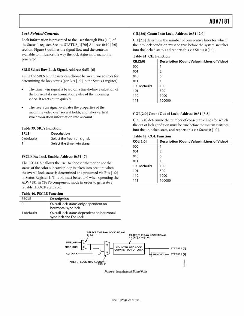
Lock Related Controls
Lock information is presented to the user through Bits [1:0] of the Status 1 register. See the STATUS_1[7:0] Address 0x10 [7:0] section. Figure 8 outlines the signal flow and the controls available to influence the way the lock status information is generated.
SRLS Select Raw Lock Signal, Address 0x51 [6]
Using the SRLS bit, the user can choose between two sources for determining the lock status (per Bits [1:0] in the Status 1 register).
• The time_win signal is based on a line-to-line evaluation of the horizontal synchronization pulse of the incoming video. It reacts quite quickly.
• The free_run signal evaluates the properties of the incoming video over several fields, and takes vertical synchronization information into account.
Table 39. SRLS Function SRLS Description 0 (default) Select the free_run signal. 1 Select the time_win signal.
FSCLE Fsc Lock Enable, Address 0x51 [7]
The FSCLE bit allows the user to choose whether or not the status of the color subcarrier loop is taken into account when the overall lock status is determined and presented via Bits [1:0] in Status Register 1. This bit must be set to 0 when operating the ADV7181 in YPrPb component mode in order to generate a reliable HLOCK status bit.
Table 40. FSCLE Function FSCLE Description 0 Overall lock status only dependent on
horizontal sync lock. 1 (default) Overall lock status dependent on horizontal
sync lock and Fsc Lock.
CIL[2:0] Count Into Lock, Address 0x51 [2:0]
CIL[2:0] determine the number of consecutive lines for which the into lock condition must be true before the system switches into the locked state, and reports this via Status 0 [1:0].
Table 41. CIL Function CIL[2:0] Description (Count Value in Lines of Video) 000 1 001 2 010 5 011 10 100 (default) 100 101 500 110 1000 111 100000
COL[2:0] Count Out of Lock, Address 0x51 [5:3]
COL[2:0] determine the number of consecutive lines for which the out of lock condition must be true before the system switches into the unlocked state, and reports this via Status 0 [1:0].
Table 42. COL Function COL[2:0] Description (Count Value in Lines of Video) 000 1 001 2 010 5 011 10 100 (default) 100 101 500 110 1000 111 100000
0482
0-00
8
1
0
TIME_WIN
FREE_RUN STATUS 1 [0]
SELECT THE RAW LOCK SIGNALSRLS FILTER THE RAW LOCK SIGNAL
CIL[2:0], COL[2:0]
TAKE FSC LOCK INTO ACCOUNTFSCLE
STATUS 1 [1]FSC LOCK1
0COUNTER INTO LOCK
COUNTER OUT OF LOCK
MEMORY
Figure 8. Lock Related Signal Path
ADV7181
Rev. B | Page 24 of 104
COLOR CONTROLS The following registers provide user control over the picture appearance, including control of the active data in the event of video being lost. They are independent of any other controls. For instance, brightness control is independent from picture clamping, although both controls affect the signal’s dc level.
CON[7:0] Contrast Adjust, Address 0x08 [7:0]
This register allows the user to adjust the contrast of the picture.
Table 43. CON Function CON[7:0] Description
(Adjust Contrast of the Picture) 0x80 (default) Gain on luma channel = 1. 0x00 Gain on luma channel = 0. 0xFF Gain on luma channel = 2.
SAT[7:0] Saturation Adjust, Address 0x09 [7:0]
The user can adjust the saturation of the color output using this register.
ADI encourages users not to use the SAT[7:0] register, which may be removed in future revisions of the ADV7181. Instead, the SD_SAT_Cb and SD_SAT_Cr registers should be used.
Table 44. SAT Function SAT[7:0] Description
(Adjust Saturation of the Picture) 0x80 (default) Chroma gain = 0 dB. 0x00 Chroma gain = –42 dB. 0xFF Chroma gain = 6 dB.
SD_SAT_Cb[7:0] SD Saturation Cb Channel, Address 0xE3 [7:0]
This register allows the user to control the gain of the Cb channel only.
For this register to be active, SAT[7:0] must be programmed with its default value of 0x80. If SAT[7:0] is programmed with a different value, SD_SAT_Cb[7:0] and SD_SAT_Cr[7:0] are inactive.
Table 45. SD_SAT_Cb Function
SD_SAT_Cb[7:0] Description (Adjust Saturation of the Picture)
0x80 (defualt) Gain on Cb channel = 0 dB. 0x00 Gain on Cb channel = –42 dB. 0xFF Gain on Cb channel = +6 dB.
SD_SAT_Cr[7:0] SD Saturation Cr Channel, Address 0xE4 [7:0]
This register allows the user to control the gain of the Cr channel only.
For this register to be active, SAT[7:0] must be programmed with its default value of 0x80. If SAT[7:0] is programmed with a different value, SD_SAT_Cb[7:0] and SD_SAT_Cr[7:0] are inactive.
Table 46. SD_SAT_Cr Function
SD_SAT_Cr[7:0] Description (Adjust Saturation of the Picture)
0x80 (default) Gain on Cr channel = 0 dB. 0x00 Gain on Cr channel = –42 dB. 0xFF Gain on Cr channel = +6 dB.
SD_OFF_Cb[7:0] SD Offset Cb Channel, Address 0xE1 [7:0]
This register allows the user to select an offset for the Cb channel only. There is a functional overlap with the Hue [7:0] register.
Table 47.SD_OFF_Cb Function
SD_OFF_Cb[7:0]
Description (Adjust Hue of the Picture by Selecting an Offset for Data on the Cb Channel)
0x80 (default) 0 offset applied to the Cb channel. 0x00 –312 mV offset applied to the Cb channel. 0xFF +312 mV offset applied to the Cb channel.
SD_OFF_Cr [7:0] SD Offset Cr Channel, Address 0xE2 [7:0]
This register allows the user to select an offset for the Cr channel only. There is a functional overlap with the Hue [7:0] register.
Table 48. SD_OFF_Cr Function
SD_OFF_Cr[7:0]
Description (Adjust Hue of the Picture by Selecting an Offset for Data on Cr Channel)
0x80 (default) 0 offset applied to the Cb channel. 0x00 –312 mV offset applied to the Cr channel. 0xFF +312 mV offset applied to the Cr channel.
ADV7181
Rev. B | Page 25 of 104
BRI[7:0] Brightness Adjust, Address 0x0A [7:0]
This register controls the brightness of the video signal through the ADV7181.
Table 49. BRI Function BRI[7:0] Description
(Adjust Brightness of the Picture) 0x00 (default) Offset of the luma channel = 0IRE. 0x7F Offset of the luma channel = 100IRE. 0x80 Offset of the luma channel = –100IRE.
HUE[7:0] Hue Adjust, Address 0x0B [7:0]
This register contains the value for the color hue adjustment.
HUE[7:0] has a range of ±90°, with 0x00 equivalent to an adjustment of 0°. The resolution of HUE[7:0] is 1 bit = 0.7°.
The hue adjustment value is fed into the AM color demodulation block. Therefore, it only applies to video signals that contain chroma information in the form of an AM modulated carrier (CVBS or Y/C in PAL or NTSC). It does not affect SECAM and does not work on component video inputs (YPrPb).
Table 50. HUE Function HUE[7:0] Description (Adjust Hue of the Picture) 0x00 (default) Phase of the chroma signal = 0°. 0x7F Phase of the chroma signal = +90°. 0x80 Phase of the chroma signal = –90°.
DEF_Y[5:0] Default Value Y, Address 0x0C [7:2]
When the ADV7181 loses lock on the incoming video signal or when there is no input signal, the DEF_Y[5:0] register allows the user to specify a default luma value to be output.
This value is used under the following conditions:
• If DEF_VAL_AUTO_EN bit is set to high and the ADV7181 lost lock to the input video signal. This is the intended mode of operation (automatic mode).
• The DEF_VAL_EN bit is set, regardless of the lock status of the video decoder. This is a forced mode that may be useful during configuration.
The DEF_Y[5:0] values define the 6 MSBs of the output video. The remaining LSBs are padded with 0s. For example, in 8-bit mode, the output is Y[7:0] = DEF_Y[5:0], 0, 0.
Table 51. DEF_Y Function DEF_Y[5:0] Description 0x0D (blue) (default) Default value of Y.
DEF_C[7:0] Default Value C, Address 0x0D [7:0]
The DEF_C[7:0] register complements the DEF_Y[5:0] value. It defines the 4 MSBs of Cr and Cb values to be output if
• The DEF_VAL_AUTO_EN bit is set to high and the ADV7181 can’t lock to the input video (automatic mode).
• DEF_VAL_EN bit is set to high (forced output).
The data that is finally output from the ADV7181 for the chroma side is Cr[7:0] = DEF_C[7:4], 0, 0, 0, 0, Cb[7:0] = DEF_C[3:0], 0, 0, 0, 0.
Table 52. DEF_C Function DEF_C[7:0] Description 0x7C (blue) (default) Default values for Cr and Cb.
DEF_VAL_EN Default Value Enable, Address 0x0C [0]
This bit forces the use of the default values for Y, Cr, and Cb. Refer to the descriptions for DEF_Y and DEF_C for additional information. The decoder also outputs a stable 27 MHz clock, HS, and VS in this mode.
Table 53. DEF_VAL_EN Function DEF_VAL_EN Description 0 (default) Don't force the use of default Y, Cr, and
Cb values. Output colors dependent on DEF_VAL_AUTO_EN.
1 Always use default Y, Cr, and Cb values. Override picture data even if the video decoder is locked.
DEF_VAL_AUTO_EN Default Value Automatic Enable, Address 0x0C [1]
This bit enables the automatic usage of the default values for Y, Cr, and Cb when the ADV7181 cannot lock to the video signal.
Table 54. DEF_VAL_AUTO_EN Function DEF_VAL_AUTO_EN Description 0 Don't use default Y, Cr, and Cb values. If
unlocked, output noise. 1 (default) Use default Y, Cr, and Cb values when
the decoder loses lock.
ADV7181
Rev. B | Page 26 of 104
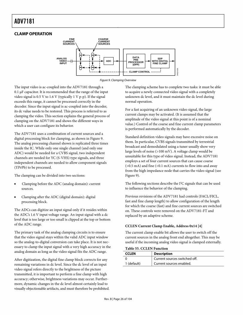
CLAMP OPERATION
0482
0-00
9
COARSECURRENTSOURCES
FINECURRENTSOURCES
DATAPRE
PROCESSOR(DPP)
ADCSDP
WITH DIGITALFINE CLAMP
CLAMP CONTROL
ANALOGVIDEOINPUT
Figure 9. Clamping Overview
The input video is ac-coupled into the ADV7181 through a 0.1 µF capacitor. It is recommended that the range of the input video signal is 0.5 V to 1.6 V (typically 1 V p-p). If the signal exceeds this range, it cannot be processed correctly in the decoder. Since the input signal is ac-coupled into the decoder, its dc value needs to be restored. This process is referred to as clamping the video. This section explains the general process of clamping on the ADV7181 and shows the different ways in which a user can configure its behavior.
The ADV7181 uses a combination of current sources and a digital processing block for clamping, as shown in Figure 9. The analog processing channel shown is replicated three times inside the IC. While only one single channel (and only one ADC) would be needed for a CVBS signal, two independent channels are needed for YC (S-VHS) type signals, and three independent channels are needed to allow component signals (YPrPb) to be processed.
The clamping can be divided into two sections:
• Clamping before the ADC (analog domain): current sources.
• Clamping after the ADC (digital domain): digital processing block.
The ADCs can digitize an input signal only if it resides within the ADC’s 1.6 V input voltage range. An input signal with a dc level that is too large or too small is clipped at the top or bottom of the ADC range.
The primary task of the analog clamping circuits is to ensure that the video signal stays within the valid ADC input window so the analog-to-digital conversion can take place. It is not nec-essary to clamp the input signal with a very high accuracy in the analog domain as long as the video signal fits the ADC range.
After digitization, the digital fine clamp block corrects for any remaining variations in dc level. Since the dc level of an input video signal refers directly to the brightness of the picture transmitted, it is important to perform a fine clamp with high accuracy; otherwise, brightness variations may occur. Further-more, dynamic changes in the dc level almost certainly lead to visually objectionable artifacts, and must therefore be prohibited.
The clamping scheme has to complete two tasks: it must be able to acquire a newly connected video signal with a completely unknown dc level, and it must maintain the dc level during normal operation.
For a fast acquiring of an unknown video signal, the large current clamps may be activated. (It is assumed that the amplitude of the video signal at this point is of a nominal value.) Control of the coarse and fine current clamp parameters is performed automatically by the decoder.
Standard definition video signals may have excessive noise on them. In particular, CVBS signals transmitted by terrestrial broadcast and demodulated using a tuner usually show very large levels of noise (>100 mV). A voltage clamp would be unsuitable for this type of video signal. Instead, the ADV7181 employs a set of four current sources that can cause coarse (>0.5 mA) and fine (<0.1 mA) currents to flow into and away from the high impedance node that carries the video signal (see Figure 9).
The following sections describe the I2C signals that can be used to influence the behavior of the clamping.
Previous revisions of the ADV7181 had controls (FACL/FICL, fast and fine clamp length) to allow configuration of the length for which the coarse (fast) and fine current sources are switched on. These controls were removed on the ADV7181-FT and replaced by an adaptive scheme.
CCLEN Current Clamp Enable, Address 0x14 [4]
The current clamp enable bit allows the user to switch off the current sources in the analog front end altogether. This may be useful if the incoming analog video signal is clamped externally.
Table 55. CCLEN Function CCLEN Description 0 Current sources switched off. 1 (default) Current sources enabled.
ADV7181
Rev. B | Page 27 of 104
DCT[1:0] Digital Clamp Timing, Address 0x15 [6:5]
The Clamp Timing register determines the time constant of the digital fine clamp circuitry. It is important to realize that the digital fine clamp reacts very fast since it is supposed to immediately correct any residual dc level error for the active line. The time constant of the digital fine clamp must be much quicker than the one from the analog blocks.
By default, the time constant of the digital fine clamp is adjusted dynamically to suit the currently connected input signal.
Table 56. DCT Function DCT[1:0] Description 00 Slow (TC = 1 sec). 01 Medium (TC = 0.5 sec). 10 (default) Fast (TC = 0.1 sec). 11 Determined by ADV7181 depending on video
parameters.
DCFE Digital Clamp Freeze Enable, Address 0x15 [4]
This register bit allows the user to freeze the digital clamp loop at any time. It is intended for users who would like to do their own clamping. Users should disable the current sources for analog clamping via the appropriate register bits, wait until the digital clamp loop settles, and then freeze it via the DCFE bit.
Table 57. DCFE Function DCFE Description 0 (default) Digital clamp operational. 1 Digital clamp loop frozen.
LUMA FILTER Data from the digital fine clamp block is processed by three sets of filters. The data format at this point is CVBS for CVBS input or luma only for Y/C and YPrPb input formats.
• Luma antialias filter (YAA). The ADV7181 receives video at a rate of 27 MHz. (In the case of 4× oversampled video, the ADCs sample at 54 MHz, and the first decimation is performed inside the DPP filters. Therefore, the data rate into the ADV7181 is always 27 MHz.) The ITU-R BT.601 recommends a sampling frequency of 13.5 MHz. The luma antialias filter decimates the oversampled video using a high quality, linear phase, low-pass filter that preserves the luma signal while at the same time attenuating out-of-band components. The luma antialias filter (YAA) has a fixed response.
• Luma shaping filters (YSH). The shaping filter block is a programmable low-pass filter with a wide variety of responses. It can be used to selectively reduce the luma
video signal bandwidth (needed prior to scaling, for example). For some video sources that contain high frequency noise, reducing the bandwidth of the luma signal improves visual picture quality. A follow-on video compression stage may work more efficiently if the video is low-pass filtered.
The ADV7181 allows selection of two responses for the shaping filter: one that is used for good quality CVBS, component, and S-VHS type sources, and a second for nonstandard CVBS signals.
The YSH filter responses also include a set of notches for PAL and NTSC. However, it is recommended to use the comb filters for YC separation.
• Digital resampling filter. This block is used to allow dynamic resampling of the video signal to alter parameters such as the time base of a line of video. Fundamentally, the resam-pler is a set of low-pass filters. The actual response is chosen by the system with no requirement for user intervention.
Figure 11 through Figure 14 show the overall response of all filters together. Unless otherwise noted, the filters are set into a typical wideband mode.
Y Shaping Filter
For input signals in CVBS format, the luma shaping filters play an essential role in removing the chroma component from a composite signal. YC separation must aim for best possible crosstalk reduction while still retaining as much bandwidth (especially on the luma component) as possible. High quality YC separation can be achieved by using the internal comb filters of the ADV7181. Comb filtering, however, relies on the frequency relationship of the luma component (multiples of the video line rate) and the color subcarrier (Fsc). For good quality CVBS signals, this relationship is known; the comb filter algorithms can be used to separate out luma and chroma with high accuracy.
In the case of nonstandard video signals, the frequency relationship may be disturbed and the comb filters may not be able to remove all crosstalk artifacts in an optimum fashion without the assistance of the shaping filter block.
An automatic mode is provided. Here, the ADV7181 evaluates the quality of the incoming video signal and selects the filter responses in accordance with the signal quality and video standard. YFSM, WYSFMOVR, and WYSFM allow the user to manually override the automatic decisions in part or in full.
ADV7181
Rev. B | Page 28 of 104
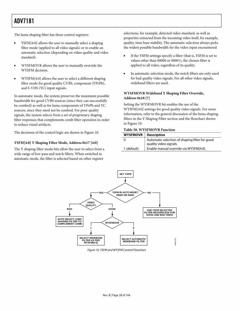
The luma shaping filter has three control registers:
• YSFM[4:0] allows the user to manually select a shaping filter mode (applied to all video signals) or to enable an automatic selection (depending on video quality and video standard).
• WYSFMOVR allows the user to manually override the WYSFM decision.
• WYSFM[4:0] allows the user to select a different shaping filter mode for good quality CVBS, component (YPrPb), and S-VHS (YC) input signals.
In automatic mode, the system preserves the maximum possible bandwidth for good CVBS sources (since they can successfully be combed) as well as for luma components of YPrPb and YC sources, since they need not be combed. For poor quality signals, the system selects from a set of proprietary shaping filter responses that complements comb filter operation in order to reduce visual artifacts.
The decisions of the control logic are shown in Figure 10.
YSFM[4:0] Y Shaping Filter Mode, Address 0x17 [4:0]
The Y shaping filter mode bits allow the user to select from a wide range of low-pass and notch filters. When switched in automatic mode, the filter is selected based on other register
selections, for example, detected video standard, as well as properties extracted from the incoming video itself, for example, quality, time base stability. The automatic selection always picks the widest possible bandwidth for the video input encountered.
• If the YSFM settings specify a filter (that is, YSFM is set to values other than 00000 or 00001), the chosen filter is applied to all video, regardless of its quality.
• In automatic selection mode, the notch filters are only used for bad quality video signals. For all other video signals, wideband filters are used.
WYSFMOVR Wideband Y Shaping Filter Override, Address 0x18 [7]
Setting the WYSFMOVR bit enables the use of the WYSFM[4:0] settings for good quality video signals. For more information, refer to the general discussion of the luma shaping filters in the Y Shaping Filter section and the flowchart shown in Figure 10.
Table 58. WYSFMOVR Function WYSFMOVR Description 0 Automatic selection of shaping filter for good
quality video signals. 1 (default) Enable manual override via WYSFM[4:0].
0482
0-01
0
AUTO SELECT LUMASHAPING FILTER TOCOMPLEMENT COMB
SET YSFM
YSFM IN AUTO MODE?00000 OR 00001
VIDEOQUALITY
BAD GOOD
SELECT WIDEBANDFILTER AS PER
WYSFM[4:0]SELECT AUTOMATICWIDEBAND FILTER
WYSFMOVR
1 0
USE YSFM SELECTEDFILTER REGARDLESS FOR
GOOD AND BAD VIDEO
YES NO
Figure 10. YSFM and WYSFM Control Flowchart
ADV7181
Rev. B | Page 29 of 104
Table 59. YSFM Function YSFM[4:0] Description 0'0000 Automatic selection including a wide notch
response (PAL/NTSC/SECAM) 0'0001 (default)
Automatic selection including a narrow notch response (PAL/NTSC/SECAM)
0'0010 SVHS 1 0'0011 SVHS 2 0'0100 SVHS 3 0'0101 SVHS 4 0'0110 SVHS 5 0'0111 SVHS 6 0'1000 SVHS 7 0'1001 SVHS 8 0'1010 SVHS 9 0'1011 SVHS 10 0'1100 SVHS 11 0'1101 SVHS 12 0'1110 SVHS 13 0'1111 SVHS 14 1'0000 SVHS 15 1'0001 SVHS 16 1'0010 SVHS 17 1'0011 SVHS 18 (CCIR 601) 1'0100 PAL NN 1 1'0101 PAL NN 2 1'0110 PAL NN 3 1'0111 PAL WN 1 1'1000 PAL WN 2 1'1001 NTSC NN 1 1'1010 NTSC NN 2 1'1011 NTSC NN 3 1'1100 NTSC WN 1 1'1101 NTSC WN 2 1'1110 NTSC WN 3 1'1111 Reserved.
WYSFM[4:0] Wide Band Y Shaping Filter Mode, Address 0x18 [4:0]
The WYSFM[4:0] bits allow the user to manually select a shaping filter for good quality video signals, for example, CVBS with stable time base, luma component of YPrPb, luma component of YC. The WYSFM bits are only active if the WYSFMOVR bit is set to 1. See the general discussion of the shaping filter settings in the Y Shaping Filter section.
Table 60. WYSFM Function WYSFM[4:0] Description 0'0000 Do not use 0'0001 Do not use 0'0010 SVHS 1 0'0011 SVHS 2 0'0100 SVHS 3 0'0101 SVHS 4 0'0110 SVHS 5 0'0111 SVHS 6 0'1000 SVHS 7 0'1001 SVHS 8 0'1010 SVHS 9 0'1011 SVHS 10 0'1100 SVHS 11 0'1101 SVHS 12 0'1110 SVHS 13 0'1111 SVHS 14 1'0000 SVHS 15 1'0001 SVHS 16 1'0010 SVHS 17 1'0011 (default) SVHS 18 (CCIR 601) 1'0100–1’1111 Do not use
0
–10
–20
–30
–40
–50
–60
–700 108642 12
0482
0-01
1
FREQUENCY (MHz)
COMBINED Y ANTIALIAS, S-VHS LOW-PASS FILTERS,Y RESAMPLE
AM
PLIT
UD
E (d
B)
Figure 11. Y S-VHS Combined Responses
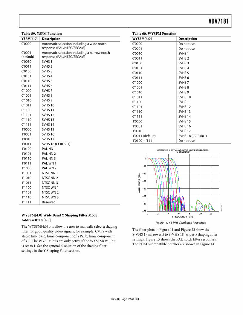
The filter plots in Figure 11 and Figure 22 show the S-VHS 1 (narrowest) to S-VHS 18 (widest) shaping filter settings. Figure 13 shows the PAL notch filter responses. The NTSC-compatible notches are shown in Figure 14.
ADV7181
Rev. B | Page 30 of 104
0
–20
–40
–60
–80
–100
–1200 108642 12
0482
0-01
2
FREQUENCY (MHz)
AM
PLIT
UD
E (d
B)
COMBINED Y ANTIALIAS, CCIR MODE SHAPING FILTER,Y RESAMPLE
Figure 12. Y S-VHS 18 Extra Wideband Filter (CCIR 601-Compliant)
0
–10
–20
–30
–40
–50
–60
–700 108642 12
0482
0-01
3
FREQUENCY (MHz)
COMBINED Y ANTIALIAS, PAL NOTCH FILTERS,Y RESAMPLE
AM
PLIT
UD
E (d
B)
Figure 13. Pal Notch Filter Response
0
–10
–20
–30
–40
–50
–60
–700 108642 12
0482
0-01
4
FREQUENCY (MHz)
COMBINED Y ANTIALIAS, NTSC NOTCH FILTERS,Y RESAMPLE
AM
PLIT
UD
E (d
B)
Figure 14. NTSC Notch Filter Response
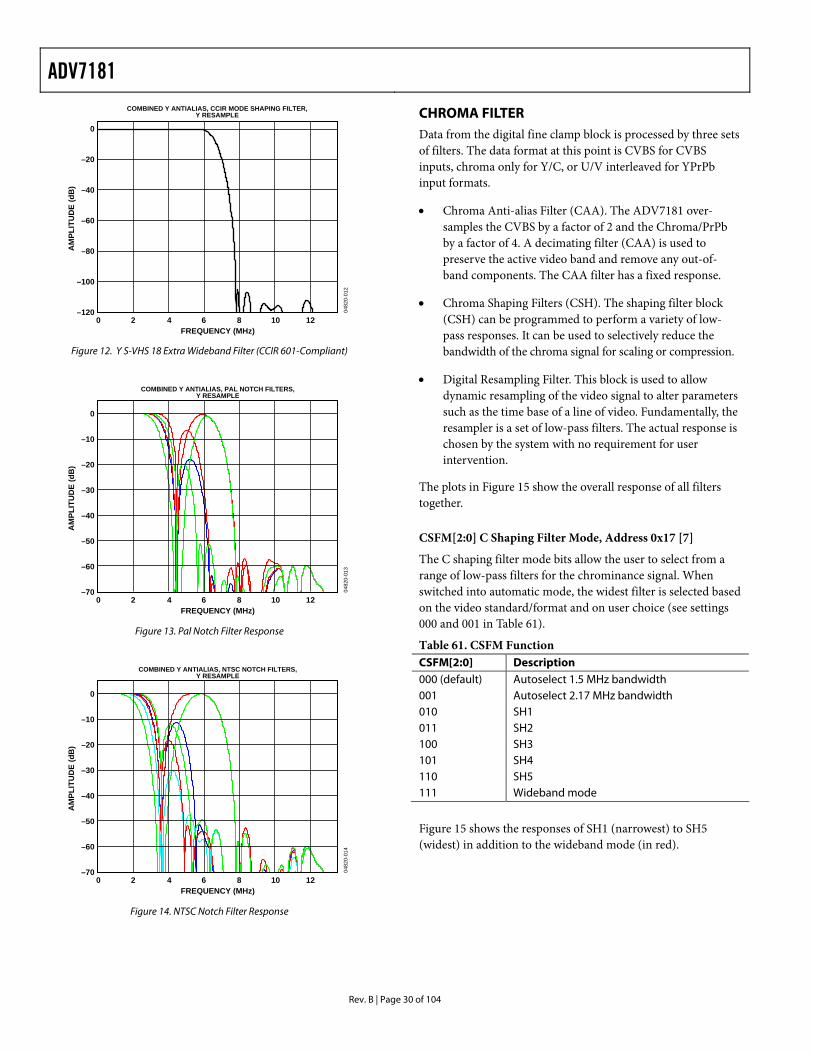
CHROMA FILTER Data from the digital fine clamp block is processed by three sets of filters. The data format at this point is CVBS for CVBS inputs, chroma only for Y/C, or U/V interleaved for YPrPb input formats.
• Chroma Anti-alias Filter (CAA). The ADV7181 over-samples the CVBS by a factor of 2 and the Chroma/PrPb by a factor of 4. A decimating filter (CAA) is used to preserve the active video band and remove any out-of-band components. The CAA filter has a fixed response.
• Chroma Shaping Filters (CSH). The shaping filter block (CSH) can be programmed to perform a variety of low-pass responses. It can be used to selectively reduce the bandwidth of the chroma signal for scaling or compression.
• Digital Resampling Filter. This block is used to allow dynamic resampling of the video signal to alter parameters such as the time base of a line of video. Fundamentally, the resampler is a set of low-pass filters. The actual response is chosen by the system with no requirement for user intervention.
The plots in Figure 15 show the overall response of all filters together.
CSFM[2:0] C Shaping Filter Mode, Address 0x17 [7]
The C shaping filter mode bits allow the user to select from a range of low-pass filters for the chrominance signal. When switched into automatic mode, the widest filter is selected based on the video standard/format and on user choice (see settings 000 and 001 in Table 61).
Table 61. CSFM Function CSFM[2:0] Description 000 (default) Autoselect 1.5 MHz bandwidth 001 Autoselect 2.17 MHz bandwidth 010 SH1 011 SH2 100 SH3 101 SH4 110 SH5 111 Wideband mode
Figure 15 shows the responses of SH1 (narrowest) to SH5 (widest) in addition to the wideband mode (in red).
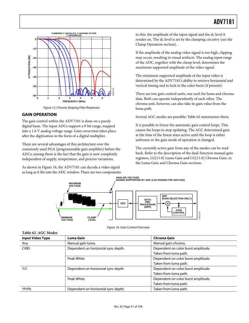
ADV7181
Rev. B | Page 31 of 104
0
–10
–20
–30
–40
–50
–600 54321 6
0482
0-01
5
FREQUENCY (MHz)
COMBINED C ANTIALIAS, C SHAPING FILTER,C RESAMPLER
ATT
ENU
ATI
ON
(dB
)
Figure 15. Chroma Shaping Filter Responses
GAIN OPERATION The gain control within the ADV7181 is done on a purely digital basis. The input ADCs support a 9-bit range, mapped into a 1.6 V analog voltage range. Gain correction takes place after the digitization in the form of a digital multiplier.
There are several advantages of this architecture over the commonly used PGA (programmable gain amplifier) before the ADCs; among them is the fact that the gain is now completely independent of supply, temperature, and process variations.
As shown in Figure 16, the ADV7181 can decode a video signal as long as it fits into the ADC window. There are two components
to this: the amplitude of the input signal and the dc level it resides on. The dc level is set by the clamping circuitry (see the Clamp Operation section).
If the amplitude of the analog video signal is too high, clipping may occur, resulting in visual artifacts. The analog input range of the ADC, together with the clamp level, determines the maximum supported amplitude of the video signal.
The minimum supported amplitude of the input video is determined by the ADV7181’s ability to retrieve horizontal and vertical timing and to lock to the color burst (if present).
There are two gain control units, one each for luma and chroma data. Both can operate independently of each other. The chroma unit, however, can also take its gain value from the luma path.
Several AGC modes are possible; Table 62 summarizes them.
It is possible to freeze the automatic gain control loops. This causes the loops to stop updating. The AGC determined gain at the time of the freeze stays active until the loop is either unfrozen or the gain mode of operation is changed.
The currently active gain from any of the modes can be read back. Refer to the description of the dual-function manual gain registers, LG[11:0] Luma Gain and CG[11:0] Chroma Gain, in the Luma Gain and Chroma Gain sections.
0482
0-01
6
ANALOG VOLTAGERANGE SUPPORTED BY ADC (1.6V RANGE FOR ADV7181)
DATAPRE
PROCESSOR(DPP)
ADC
SDP(GAIN SELECTION ONLY)
MAXIMUMVOLTAGE
MINIMUMVOLTAGE
CLAMPLEVEL
GAINCONTROL
Figure 16. Gain Control Overview
Table 62. AGC Modes Input Video Type Luma Gain Chroma Gain Any Manual gain luma. Manual gain chroma.
Dependent on color burst amplitude. Dependent on horizontal sync depth. Taken from luma path. Dependent on color burst amplitude.
CVBS
Peak White Taken from luma path. Dependent on color burst amplitude. Dependent on horizontal sync depth. Taken from luma path. Dependent on color burst amplitude.
Y/C
Peak White. Taken from luma path.
YPrPb Dependent on horizontal sync depth. Taken from luma path.
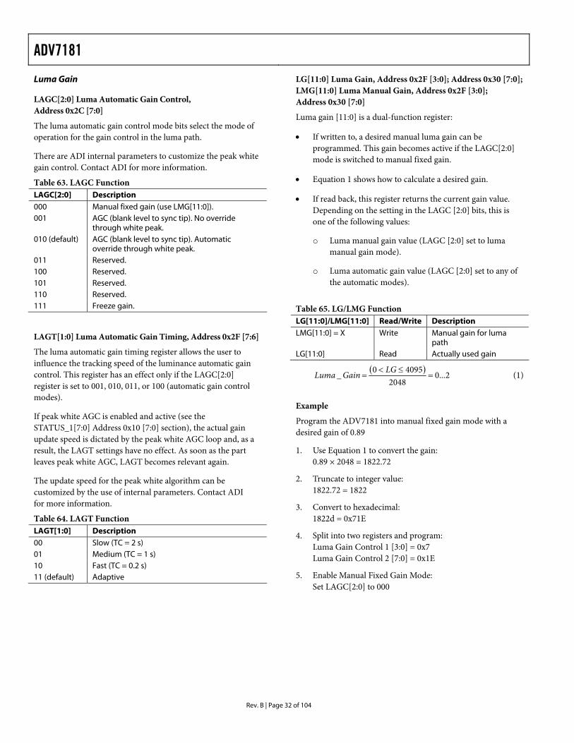
ADV7181
Rev. B | Page 32 of 104
Luma Gain
LAGC[2:0] Luma Automatic Gain Control, Address 0x2C [7:0]
The luma automatic gain control mode bits select the mode of operation for the gain control in the luma path.
There are ADI internal parameters to customize the peak white gain control. Contact ADI for more information.
Table 63. LAGC Function LAGC[2:0] Description 000 Manual fixed gain (use LMG[11:0]). 001 AGC (blank level to sync tip). No override
through white peak. 010 (default) AGC (blank level to sync tip). Automatic
override through white peak. 011 Reserved. 100 Reserved. 101 Reserved. 110 Reserved. 111 Freeze gain.
LAGT[1:0] Luma Automatic Gain Timing, Address 0x2F [7:6]
The luma automatic gain timing register allows the user to influence the tracking speed of the luminance automatic gain control. This register has an effect only if the LAGC[2:0] register is set to 001, 010, 011, or 100 (automatic gain control modes).
If peak white AGC is enabled and active (see the STATUS_1[7:0] Address 0x10 [7:0] section), the actual gain update speed is dictated by the peak white AGC loop and, as a result, the LAGT settings have no effect. As soon as the part leaves peak white AGC, LAGT becomes relevant again.
The update speed for the peak white algorithm can be customized by the use of internal parameters. Contact ADI for more information.
Table 64. LAGT Function LAGT[1:0] Description 00 Slow (TC = 2 s) 01 Medium (TC = 1 s) 10 Fast (TC = 0.2 s) 11 (default) Adaptive
LG[11:0] Luma Gain, Address 0x2F [3:0]; Address 0x30 [7:0]; LMG[11:0] Luma Manual Gain, Address 0x2F [3:0]; Address 0x30 [7:0]
Luma gain [11:0] is a dual-function register:
• If written to, a desired manual luma gain can be programmed. This gain becomes active if the LAGC[2:0] mode is switched to manual fixed gain.
• Equation 1 shows how to calculate a desired gain.
• If read back, this register returns the current gain value. Depending on the setting in the LAGC [2:0] bits, this is one of the following values:
o Luma manual gain value (LAGC [2:0] set to luma manual gain mode).
o Luma automatic gain value (LAGC [2:0] set to any of the automatic modes).
Table 65. LG/LMG Function LG[11:0]/LMG[11:0] Read/Write Description LMG[11:0] = X Write Manual gain for luma
path LG[11:0] Read Actually used gain
( ) 2...02048
40950_ =≤<
=LGGainLuma (1)
Example
Program the ADV7181 into manual fixed gain mode with a desired gain of 0.89
1. Use Equation 1 to convert the gain: 0.89 × 2048 = 1822.72
2. Truncate to integer value: 1822.72 = 1822
3. Convert to hexadecimal: 1822d = 0x71E
4. Split into two registers and program: Luma Gain Control 1 [3:0] = 0x7 Luma Gain Control 2 [7:0] = 0x1E
5. Enable Manual Fixed Gain Mode: Set LAGC[2:0] to 000
ADV7181
Rev. B | Page 33 of 104
BETACAM Enable Betacam Levels, Address 0x01 [5]
If YPrPb data is routed through the ADV7181, the automatic gain control modes can target different video input levels, as outlined in Table 70. The BETACAM bit is valid only if the input mode is YPrPb (component). The BETACAM bit sets the target value for AGC operation.
A review of the following sections is useful:
• SETADC_sw_man_en, Manual Input Muxing Enable, Address C4 [7] to find how component video (YPrPb) can be routed through the ADV7181.
• Video Standard Selection to select the various standards, for example, with and without pedestal.
The automatic gain control (AGC) algorithms adjust the levels based on the setting of the BETACAM bit (see Table 66.).
Table 66. BETACAM Function BETACAM Description 0 (default) Assuming YPrPb is selected as input format. Selecting PAL with pedestal selects MII. Selecting PAL without pedestal selects SMPTE. Selecting NTSC with pedestal selects MII. Selecting NTSC without pedestal selects SMPTE. 1 Assuming YPrPb is selected as input format. Selecting PAL with pedestal selects BETACAM. Selecting PAL without pedestal selects BETACAM
variant. Selecting NTSC with pedestal selects BETACAM. Selecting NTSC without pedestal selects BETACAM
variant.
PW_UPD Peak White Update, Address 0x2B [0]
The peak white and average video algorithms determine the gain based on measurements taken from the active video. The PW_UPD bit determines the rate of gain change. LAGC[2:0] must be set to the appropriate mode to enable the peak white or average video mode in the first place. For more information, refer to the LAGC[2:0] Luma Automatic Gain Control, Address 0x2C [7:0] section.
Table 67. PW_UPD Function PW_UPD Description 0 Update gain once per video line. 1 (default) Update gain once per field.
Chroma Gain
CAGC[1:0] Chroma Automatic Gain Control, Address 0x2C [1:0]
The two bits of Color Automatic Gain Control mode select the basic mode of operation for automatic gain control in the chroma path.
Table 68. CAGC Function CAGC[1:0] Description 00 Manual fixed gain (use CMG[11:0]). 01 Use luma gain for chroma. 10 (default) Automatic gain (based on color burst). 11 Freeze chroma gain.
CAGT[1:0] Chroma Automatic Gain Timing, Address 0x2D [7:6]
The Chroma Automatic Gain Timing register allows the user to influence the tracking speed of the chroma automatic gain control. This register has an effect only if the CAGC[1:0] register is set to 10 (automatic gain).
Table 69. CAGT Function CAGT[1:0] Description 00 Slow (TC = 2 s) 01 Medium (TC = 1 s) 10 Fast (TC = 0.2 s) 11 (default) Adaptive
Table 70. Betacam Levels Name Betacam (mV) Betacam Variant (mV) SMPTE (mV) MII (mV) Y Range 0 to 714 (incl. 7.5% pedestal) 0 to 714 0 to 700 0 to 700 (incl. 7.5% pedestal) Pb and Pr Range –467 to +467 –505 to +505 –350 to +350 –324 to +324 Sync Depth 286 286 300 300
ADV7181
Rev. B | Page 34 of 104
CG[11:0] Chroma Gain, Address 0x2D [3:0]; Address 0x2E [7:0] CMG[11:0] Chroma Manual Gain, Address 0x2D [3:0]; Address 0x2E [7:0]
Chroma gain [11:0] is a dual-function register:
• If written to, a desired manual chroma gain can be programmed. This gain becomes active if the CAGC[1:0] mode is switched to manual fixed gain.
• Refer to Equation 2 for calculating a desired gain.
• If read back, this register returns the current gain value. Depending on the setting in the CAGC[1:0] bits, this is one of the following values:
o Chroma manual gain value (CAGC[1:0] set to chroma manual gain mode).
o Chroma automatic gain value (CAGC[1:0] set to any of the automatic modes).
Table 71. CG/CMG Function CG[11:0]/CMG[11:0] Read/Write Description CMG[11:0] Write Manual gain for chroma
path. CG[11:0] Read Currently active gain.
( )4...0
102440950
_ =≤<
=CGGainChroma (2)
Example
Freezing the automatic gain loop and reading back the CG[11:0] register results in a value of 0x47A.
1. Convert the read back value to decimal: 0x47A = 1146d
2. Apply Equation 2 to convert the readback value: 1146/1024 = 1.12
CKE Color Kill Enable, Address 0x2B [6]
The Color Kill Enable bit allows the optional color kill function to be switched on or off.
For QAM-based video standards (PAL and NTSC) as well as FM-based systems (SECAM), the threshold for the color kill decision is selectable via the CKILLTHR[2:0] bits.
If color kill is enabled, and if the color carrier of the incoming video signal is less than the threshold for 128 consecutive video lines, color processing is switched off (black and white output). To switch the color processing back on, another 128 consecutive lines with a color burst greater than the threshold are required.
The color kill option only works for input signals with a modu-lated chroma part. For component input (YPrPb), there is no color kill.
Table 72. CKE Function CKE Description 0 Color kill disabled. 1 (default) Color kill enabled.
CKILLTHR[2:0] Color Kill Threshold, Address 0x3D [6:4]
The CKILLTHR[2:0] bits allow the user to select a threshold for the color kill function. The threshold only applies to QAM-based (NTSC and PAL) or FM modulated (SECAM) video standards.
To enable the color kill function, the CKE bit must be set. For settings 000, 001, 010, and 011, chroma demodulation inside the ADV7181 may not work satisfactorily for poor input video signals.
Table 73. CKILLTHR Function Description CKILLTHR[2:0] SECAM NTSC, PAL 000 No color kill Kill at < 0.5% 001 Kill at < 5% Kill at < 1.5% 010 Kill at < 7% Kill at < 2.5% 011 Kill at < 8% Kill at < 4.0% 100 (default) Kill at < 9.5% Kill at < 8.5% 101 Kill at < 15% Kill at < 16.0% 110 Kill at < 32% Kill at < 32.0% 111 Reserved for ADI internal use only. Do not
select.
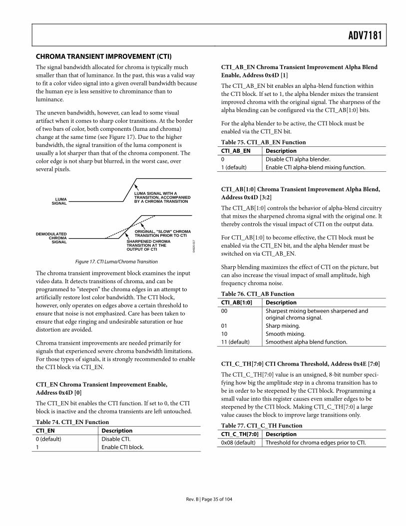
ADV7181
Rev. B | Page 35 of 104
CHROMA TRANSIENT IMPROVEMENT (CTI) The signal bandwidth allocated for chroma is typically much smaller than that of luminance. In the past, this was a valid way to fit a color video signal into a given overall bandwidth because the human eye is less sensitive to chrominance than to luminance.
The uneven bandwidth, however, can lead to some visual artifact when it comes to sharp color transitions. At the border of two bars of color, both components (luma and chroma) change at the same time (see Figure 17). Due to the higher bandwidth, the signal transition of the luma component is usually a lot sharper than that of the chroma component. The color edge is not sharp but blurred, in the worst case, over several pixels.
0482
0-01
7
LUMASIGNAL
DEMODULATEDCHROMA
SIGNAL
LUMA SIGNAL WITH ATRANSITION, ACCOMPANIEDBY A CHROMA TRANSITION
ORIGINAL, "SLOW" CHROMATRANSITION PRIOR TO CTI
SHARPENED CHROMATRANSITION AT THEOUTPUT OF CTI
Figure 17. CTI Luma/Chroma Transition
The chroma transient improvement block examines the input video data. It detects transitions of chroma, and can be programmed to “steepen” the chroma edges in an attempt to artificially restore lost color bandwidth. The CTI block, however, only operates on edges above a certain threshold to ensure that noise is not emphasized. Care has been taken to ensure that edge ringing and undesirable saturation or hue distortion are avoided.
Chroma transient improvements are needed primarily for signals that experienced severe chroma bandwidth limitations. For those types of signals, it is strongly recommended to enable the CTI block via CTI_EN.
CTI_EN Chroma Transient Improvement Enable, Address 0x4D [0]
The CTI_EN bit enables the CTI function. If set to 0, the CTI block is inactive and the chroma transients are left untouched.
Table 74. CTI_EN Function CTI_EN Description 0 (default) Disable CTI. 1 Enable CTI block.
CTI_AB_EN Chroma Transient Improvement Alpha Blend Enable, Address 0x4D [1]
The CTI_AB_EN bit enables an alpha-blend function within the CTI block. If set to 1, the alpha blender mixes the transient improved chroma with the original signal. The sharpness of the alpha blending can be configured via the CTI_AB[1:0] bits.
For the alpha blender to be active, the CTI block must be enabled via the CTI_EN bit.
Table 75. CTI_AB_EN Function CTI_AB_EN Description 0 Disable CTI alpha blender. 1 (default) Enable CTI alpha-blend mixing function.
CTI_AB[1:0] Chroma Transient Improvement Alpha Blend, Address 0x4D [3:2]
The CTI_AB[1:0] controls the behavior of alpha-blend circuitry that mixes the sharpened chroma signal with the original one. It thereby controls the visual impact of CTI on the output data.
For CTI_AB[1:0] to become effective, the CTI block must be enabled via the CTI_EN bit, and the alpha blender must be switched on via CTI_AB_EN.
Sharp blending maximizes the effect of CTI on the picture, but can also increase the visual impact of small amplitude, high frequency chroma noise.
Table 76. CTI_AB Function CTI_AB[1:0] Description 00 Sharpest mixing between sharpened and
original chroma signal. 01 Sharp mixing. 10 Smooth mixing. 11 (default) Smoothest alpha blend function.
CTI_C_TH[7:0] CTI Chroma Threshold, Address 0x4E [7:0]
The CTI_C_TH[7:0] value is an unsigned, 8-bit number speci-fying how big the amplitude step in a chroma transition has to be in order to be steepened by the CTI block. Programming a small value into this register causes even smaller edges to be steepened by the CTI block. Making CTI_C_TH[7:0] a large value causes the block to improve large transitions only.
Table 77. CTI_C_TH Function CTI_C_TH[7:0] Description 0x08 (default) Threshold for chroma edges prior to CTI.
ADV7181
Rev. B | Page 36 of 104
DIGITAL NOISE REDUCTION (DNR) Digital noise reduction is based on the assumption that high frequency signals with low amplitude are probably noise, and that their removal therefore improves picture quality.
DNR_EN Digital Noise Reduction Enable, Address 0x4D [5]
The DNR_EN bit enables the DNR block or bypasses it.
Table 78. DNR_EN Function DNR_EN Description 0 Bypass DNR (disable). 1 (default) Enable digital noise reduction on the luma data.
DNR_TH[7:0] DNR Noise Threshold, Address 0x50 [7:0]
The DNR_TH[7:0] value is an unsigned 8-bit number used to determine the maximum edge that is interpreted as noise and therefore blanked from the luma data. Programming a large value into DNR_TH[7:0] causes the DNR block to interpret even large transients as noise and remove them. The effect on the video data is therefore more visible.
Programming a small value causes only small transients to be seen as noise and to be removed.
The recommended DNR_TH[7:0] setting for A/V inputs is 0x04, and the recommended DNR_TH[7:0] setting for tuner inputs is 0x0A.
Table 79. DNR_TH Function DNR_TH[7:0] Description 0x08 (default) Threshold for maximum luma edges to be
interpreted as noise.
COMB FILTERS The comb filters of the ADV7181 have been greatly improved to automatically handle video of all types, standards, and levels of quality. Two user registers are available to customize comb filter operation.
Depending on whichever video standard has been detected (by autodetection) or selected (by manual programming), the NTSC or PAL configuration registers are used. In addition to the bits listed in this section, there are some further ADI internal controls; contact ADI for more information.
NTSC Comb Filter Settings
Used for NTSC-M/J CVBS inputs.
NSFSEL[1:0] Split Filter Selection NTSC, Address 0x19 [3:2]
The NSFSEL[1:0] control selects how much of the overall signal bandwidth is fed to the combs. A narrow split filter selection gives better performance on diagonal lines, but leaves more dot crawl in the final output image. The opposite is true for selecting a wide bandwidth split filter.
Table 80. NSFSEL Function NSFSEL[1:0] Description 00 (default) Narrow 01 Medium 10 Medium 11 Wide
CTAPSN[1:0] Chroma Comb Taps NTSC, Address 0x38 [7:6] Table 81. CTAPSN Function CTAPSN[1:0] Description 00 Do not use. 01 NTSC chroma comb adapts 3 lines (3 taps)
to 2 lines (2 taps). 10 (default) NTSC chroma comb adapts 5 lines (5 taps)
to 3 lines (3 taps). 11 NTSC chroma comb adapts 5 lines (5 taps)
to 4 lines (4 taps).
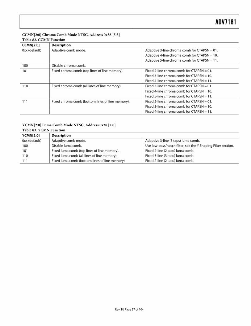
ADV7181
Rev. B | Page 37 of 104
CCMN[2:0] Chroma Comb Mode NTSC, Address 0x38 [5:3] Table 82. CCMN Function CCMN[2:0] Description
Adaptive 3-line chroma comb for CTAPSN = 01. Adaptive 4-line chroma comb for CTAPSN = 10.
0xx (default) Adaptive comb mode.
Adaptive 5-line chroma comb for CTAPSN = 11. 100 Disable chroma comb.
Fixed 2-line chroma comb for CTAPSN = 01. Fixed 3-line chroma comb for CTAPSN = 10.
101 Fixed chroma comb (top lines of line memory).
Fixed 4-line chroma comb for CTAPSN = 11. Fixed 3-line chroma comb for CTAPSN = 01. Fixed 4-line chroma comb for CTAPSN = 10.
110 Fixed chroma comb (all lines of line memory).
Fixed 5-line chroma comb for CTAPSN = 11. Fixed 2-line chroma comb for CTAPSN = 01. Fixed 3-line chroma comb for CTAPSN = 10.
111 Fixed chroma comb (bottom lines of line memory).
Fixed 4-line chroma comb for CTAPSN = 11.
YCMN[2:0] Luma Comb Mode NTSC, Address 0x38 [2:0] Table 83. YCMN Function YCMN[2:0] Description 0xx (default) Adaptive comb mode. Adaptive 3-line (3 taps) luma comb. 100 Disable luma comb. Use low-pass/notch filter; see the Y Shaping Filter section. 101 Fixed luma comb (top lines of line memory). Fixed 2-line (2 taps) luma comb. 110 Fixed luma comb (all lines of line memory). Fixed 3-line (3 taps) luma comb. 111 Fixed luma comb (bottom lines of line memory). Fixed 2-line (2 taps) luma comb.
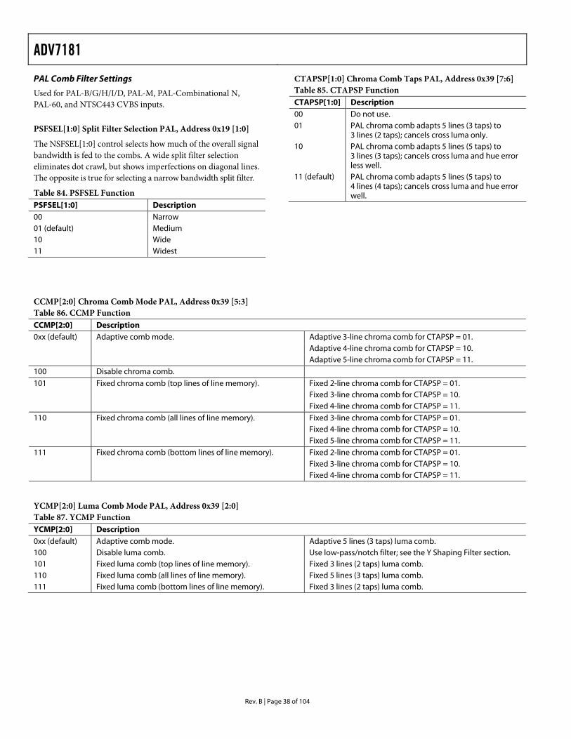
ADV7181
Rev. B | Page 38 of 104
PAL Comb Filter Settings
Used for PAL-B/G/H/I/D, PAL-M, PAL-Combinational N, PAL-60, and NTSC443 CVBS inputs.
PSFSEL[1:0] Split Filter Selection PAL, Address 0x19 [1:0]
The NSFSEL[1:0] control selects how much of the overall signal bandwidth is fed to the combs. A wide split filter selection eliminates dot crawl, but shows imperfections on diagonal lines. The opposite is true for selecting a narrow bandwidth split filter.
Table 84. PSFSEL Function PSFSEL[1:0] Description 00 Narrow 01 (default) Medium 10 Wide 11 Widest
CTAPSP[1:0] Chroma Comb Taps PAL, Address 0x39 [7:6] Table 85. CTAPSP Function CTAPSP[1:0] Description 00 Do not use. 01 PAL chroma comb adapts 5 lines (3 taps) to
3 lines (2 taps); cancels cross luma only. 10 PAL chroma comb adapts 5 lines (5 taps) to
3 lines (3 taps); cancels cross luma and hue error less well.
11 (default) PAL chroma comb adapts 5 lines (5 taps) to 4 lines (4 taps); cancels cross luma and hue error well.
CCMP[2:0] Chroma Comb Mode PAL, Address 0x39 [5:3] Table 86. CCMP Function CCMP[2:0] Description
Adaptive 3-line chroma comb for CTAPSP = 01. Adaptive 4-line chroma comb for CTAPSP = 10.
0xx (default) Adaptive comb mode.
Adaptive 5-line chroma comb for CTAPSP = 11. 100 Disable chroma comb.
Fixed 2-line chroma comb for CTAPSP = 01. Fixed 3-line chroma comb for CTAPSP = 10.
101 Fixed chroma comb (top lines of line memory).
Fixed 4-line chroma comb for CTAPSP = 11. Fixed 3-line chroma comb for CTAPSP = 01. Fixed 4-line chroma comb for CTAPSP = 10.
110 Fixed chroma comb (all lines of line memory).
Fixed 5-line chroma comb for CTAPSP = 11. Fixed 2-line chroma comb for CTAPSP = 01. Fixed 3-line chroma comb for CTAPSP = 10.
111 Fixed chroma comb (bottom lines of line memory).
Fixed 4-line chroma comb for CTAPSP = 11.
YCMP[2:0] Luma Comb Mode PAL, Address 0x39 [2:0] Table 87. YCMP Function YCMP[2:0] Description 0xx (default) Adaptive comb mode. Adaptive 5 lines (3 taps) luma comb. 100 Disable luma comb. Use low-pass/notch filter; see the Y Shaping Filter section. 101 Fixed luma comb (top lines of line memory). Fixed 3 lines (2 taps) luma comb. 110 Fixed luma comb (all lines of line memory). Fixed 5 lines (3 taps) luma comb. 111 Fixed luma comb (bottom lines of line memory). Fixed 3 lines (2 taps) luma comb.
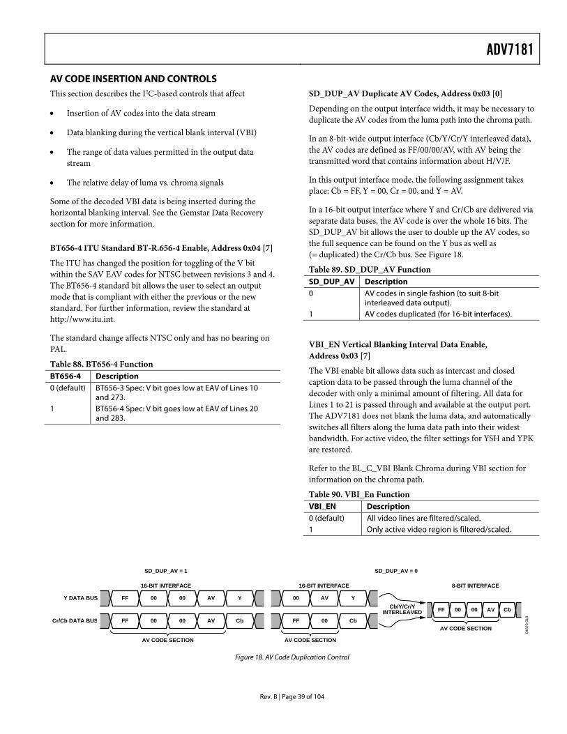
ADV7181
Rev. B | Page 39 of 104
AV CODE INSERTION AND CONTROLS This section describes the I2C-based controls that affect
• Insertion of AV codes into the data stream
• Data blanking during the vertical blank interval (VBI)
• The range of data values permitted in the output data stream
• The relative delay of luma vs. chroma signals
Some of the decoded VBI data is being inserted during the horizontal blanking interval. See the Gemstar Data Recovery section for more information.
BT656-4 ITU Standard BT-R.656-4 Enable, Address 0x04 [7]
The ITU has changed the position for toggling of the V bit within the SAV EAV codes for NTSC between revisions 3 and 4. The BT656-4 standard bit allows the user to select an output mode that is compliant with either the previous or the new standard. For further information, review the standard at http://www.itu.int.
The standard change affects NTSC only and has no bearing on PAL.
Table 88. BT656-4 Function BT656-4 Description 0 (default) BT656-3 Spec: V bit goes low at EAV of Lines 10
and 273. 1 BT656-4 Spec: V bit goes low at EAV of Lines 20
and 283.
SD_DUP_AV Duplicate AV Codes, Address 0x03 [0]
Depending on the output interface width, it may be necessary to duplicate the AV codes from the luma path into the chroma path.
In an 8-bit-wide output interface (Cb/Y/Cr/Y interleaved data), the AV codes are defined as FF/00/00/AV, with AV being the transmitted word that contains information about H/V/F.
In this output interface mode, the following assignment takes place: Cb = FF, Y = 00, Cr = 00, and Y = AV.
In a 16-bit output interface where Y and Cr/Cb are delivered via separate data buses, the AV code is over the whole 16 bits. The SD_DUP_AV bit allows the user to double up the AV codes, so the full sequence can be found on the Y bus as well as (= duplicated) the Cr/Cb bus. See Figure 18.
Table 89. SD_DUP_AV Function SD_DUP_AV Description 0 AV codes in single fashion (to suit 8-bit
interleaved data output). 1 AV codes duplicated (for 16-bit interfaces).
VBI_EN Vertical Blanking Interval Data Enable, Address 0x03 [7]
The VBI enable bit allows data such as intercast and closed caption data to be passed through the luma channel of the decoder with only a minimal amount of filtering. All data for Lines 1 to 21 is passed through and available at the output port. The ADV7181 does not blank the luma data, and automatically switches all filters along the luma data path into their widest bandwidth. For active video, the filter settings for YSH and YPK are restored.
Refer to the BL_C_VBI Blank Chroma during VBI section for information on the chroma path.
Table 90. VBI_En Function VBI_EN Description 0 (default) All video lines are filtered/scaled. 1 Only active video region is filtered/scaled.
0482
0-01
8
Y DATA BUS 00 AV YFF 00 00 AV Y
FFCr/Cb DATA BUS 00 00 AV Cb FF 00 Cb
AV CODE SECTION AV CODE SECTION
FF 00 00 AV Cb
AV CODE SECTION
Cb/Y/Cr/YINTERLEAVED
8-BIT INTERFACE16-BIT INTERFACE16-BIT INTERFACE
SD_DUP_AV = 1 SD_DUP_AV = 0
Figure 18. AV Code Duplication Control
ADV7181
Rev. B | Page 40 of 104
BL_C_VBI Blank Chroma during VBI, Address 0x04 [2]
Setting BL_C_VBI high, the Cr and Cb values of all VBI lines get blanked. This is done so any data that comes during VBI is not decoded as color and output through Cr and Cb. As a result, it should be possible to send VBI lines into the decoder, then output them through an encoder again, undistorted. Without this blanking, any wrongly decoded color is encoded by the video encoder; therefore, the VBI lines are distorted.
Table 91. BL_C_VBI Function BL_C_VBI Description 0 Decode and output color during VBI. 1 (default) Blank Cr and Cb values during VBI (no color, 0x80).
RANGE Range Selection, Address 0x04 [0]
AV codes (as per ITU-R BT-656, formerly known as CCIR-656) consist of a fixed header made up of 0xFF and 0x00 values. These two values are reserved and therefore are not to be used for active video. Additionally, the ITU also specifies that the nominal range for video should be restricted to values between 16 and 235 for luma and 16 to 240 for chroma.
The RANGE bit allows the user to limit the range of values output by the ADV7181 to the recommended value range. In any case, it is ensured that the reserved values of 255d (0xFF) and 00d (0x00) are not presented on the output pins unless they are part of an AV code header.
Table 92. RANGE Function RANGE Description 0 16 ≤ Y ≤ 235 16 ≤ C/P ≤ 240 1 (default) 1 ≤ Y ≤ 254 1 ≤ C/P ≤ 254
AUTO_PDC_EN Automatic Programmed Delay Control, Address 0x27 [6]
Enabling the AUTO_PDC_EN function activates a function within the ADV7181 that automatically programs the LTA[1:0] and CTA[2:0] to have the chroma and luma data match delays for all modes of operation. If set, manual registers LTA[1:0] and CTA[2:0] are not used by the ADV7181. If the automatic mode is disabled (via setting the AUTO_PDC_EN bit to 0), the values programmed into LTA[1:0] and CTA[2:0] registers take effect.
Table 93. AUTO_PDC_EN Function AUTO_PDC_EN Description 0 Use LTA[1:0] and CTA[2:0] values for delaying
luma and chroma samples. Refer to the LTA[1:0] Luma Timing Adjust, Address 0x27 [1:0] and CTA[2:0] Chroma Timing Adjust, Address 0x27 [5:3] sections.
1 (default) The ADV7181 automatically determines the LTA and CTA values to have luma and chroma aligned at the output.
LTA[1:0] Luma Timing Adjust, Address 0x27 [1:0]
The Luma Timing Adjust register allows the user to specify a timing difference between chroma and luma samples.
There is a certain functionality overlap with the CTA[2:0] register.
For manual programming, use the following defaults:
• CVBS input LTA[1:0] = 00
• YC input LTA[1:0] = 01
• YPrPb input LTA[1:0] = 01
Table 94. LTA Function LTA[1:0] Description 00 (default) No delay. 01 Luma 1 clk (37 ns) delayed. 10 Luma 2clk (74 ns) early. 11 Luma 1 clk (37 ns) early.
CTA[2:0] Chroma Timing Adjust, Address 0x27 [5:3]
The Chroma Timing Adjust register allows the user to specify a timing difference between chroma and luma samples. This can be used to compensate for external filter group delay differences in the luma vs. chroma path, and to allow a different number of pipeline delays while processing the video down-stream. Review this functionality together with the LTA[1:0] register.
The chroma can only be delayed/advanced in chroma pixel steps. One chroma pixel step is equal to two luma pixels. The programmable delay occurs after demodulation, where one can no longer delay by luma pixel steps.
For manual programming, use the following defaults:
• CVBS input CTA[2:0] = 011
• YC input CTA[2:0] = 101
• YPrPb input CTA[2:0] = 110
Table 95. CTA Function CTA[2:0] Description 000 Not used. 001 Chroma + 2 chroma pixel (early). 010 Chroma + 1 chroma pixel (early). 011 (default) No delay. 100 Chroma – 1 chroma pixel (late). 101 Chroma – 2 chroma pixel (late). 110 Chroma – 3 chroma pixel (late). 111 Not used.
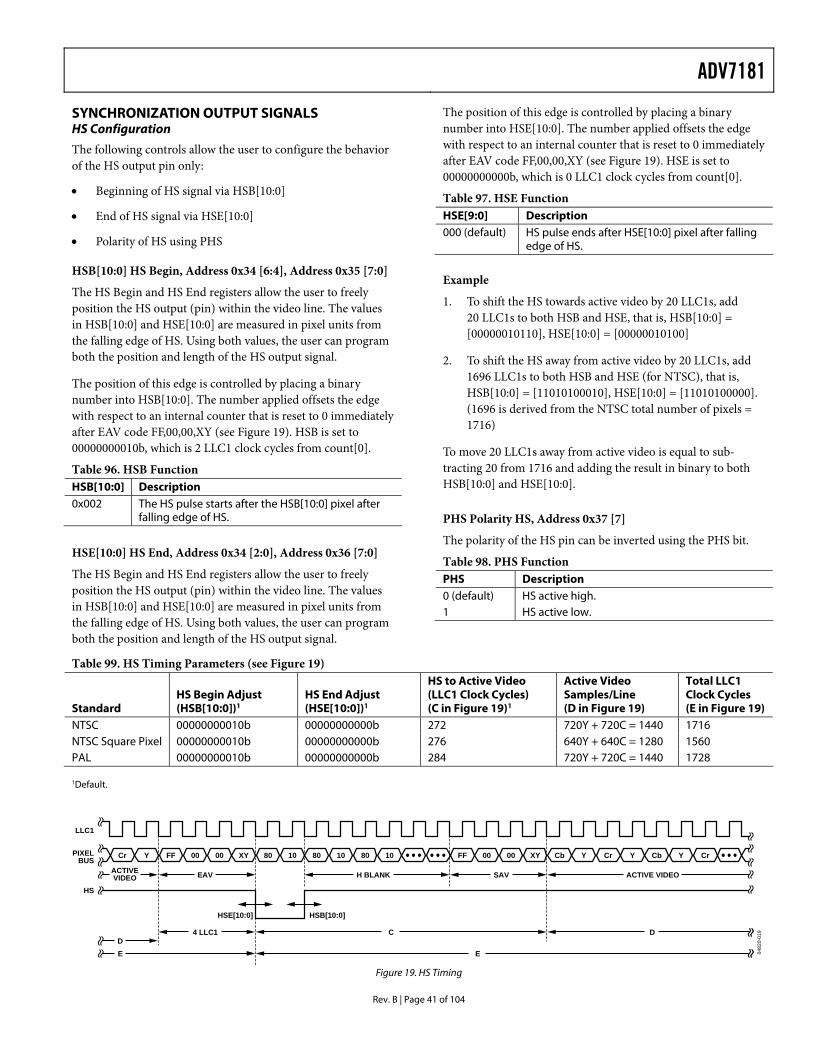
ADV7181
Rev. B | Page 41 of 104
SYNCHRONIZATION OUTPUT SIGNALS HS Configuration
The following controls allow the user to configure the behavior of the HS output pin only:
• Beginning of HS signal via HSB[10:0]
• End of HS signal via HSE[10:0]
• Polarity of HS using PHS
HSB[10:0] HS Begin, Address 0x34 [6:4], Address 0x35 [7:0]
The HS Begin and HS End registers allow the user to freely position the HS output (pin) within the video line. The values in HSB[10:0] and HSE[10:0] are measured in pixel units from the falling edge of HS. Using both values, the user can program both the position and length of the HS output signal.
The position of this edge is controlled by placing a binary number into HSB[10:0]. The number applied offsets the edge with respect to an internal counter that is reset to 0 immediately after EAV code FF,00,00,XY (see Figure 19). HSB is set to 00000000010b, which is 2 LLC1 clock cycles from count[0].
Table 96. HSB Function HSB[10:0] Description 0x002 The HS pulse starts after the HSB[10:0] pixel after
falling edge of HS.
HSE[10:0] HS End, Address 0x34 [2:0], Address 0x36 [7:0]
The HS Begin and HS End registers allow the user to freely position the HS output (pin) within the video line. The values in HSB[10:0] and HSE[10:0] are measured in pixel units from the falling edge of HS. Using both values, the user can program both the position and length of the HS output signal.
The position of this edge is controlled by placing a binary number into HSE[10:0]. The number applied offsets the edge with respect to an internal counter that is reset to 0 immediately after EAV code FF,00,00,XY (see Figure 19). HSE is set to 00000000000b, which is 0 LLC1 clock cycles from count[0].
Table 97. HSE Function HSE[9:0] Description 000 (default) HS pulse ends after HSE[10:0] pixel after falling
edge of HS.
Example
1. To shift the HS towards active video by 20 LLC1s, add 20 LLC1s to both HSB and HSE, that is, HSB[10:0] = [00000010110], HSE[10:0] = [00000010100]
2. To shift the HS away from active video by 20 LLC1s, add 1696 LLC1s to both HSB and HSE (for NTSC), that is, HSB[10:0] = [11010100010], HSE[10:0] = [11010100000]. (1696 is derived from the NTSC total number of pixels = 1716)
To move 20 LLC1s away from active video is equal to sub-tracting 20 from 1716 and adding the result in binary to both HSB[10:0] and HSE[10:0].
PHS Polarity HS, Address 0x37 [7]
The polarity of the HS pin can be inverted using the PHS bit.
Table 98. PHS Function PHS Description 0 (default) HS active high. 1 HS active low.
Table 99. HS Timing Parameters (see Figure 19)
Standard HS Begin Adjust (HSB[10:0])1
HS End Adjust (HSE[10:0])1
HS to Active Video (LLC1 Clock Cycles) (C in Figure 19)1
Active Video Samples/Line (D in Figure 19)
Total LLC1 Clock Cycles (E in Figure 19)
NTSC 00000000010b 00000000000b 272 720Y + 720C = 1440 1716 NTSC Square Pixel 00000000010b 00000000000b 276 640Y + 640C = 1280 1560 PAL 00000000010b 00000000000b 284 720Y + 720C = 1440 1728
1Default.
0482
0-01
9
E
ACTIVEVIDEO
LLC1
PIXELBUS
HS
Cr Y FF 00 00 XY 80 10 80 10 80 10 FF 00 00 XY Cb Y Cr Y Cb Y Cr
4 LLC1D
HSB[10:0]HSE[10:0]
C
E
D
SAV ACTIVE VIDEOH BLANKEAV
Figure 19. HS Timing
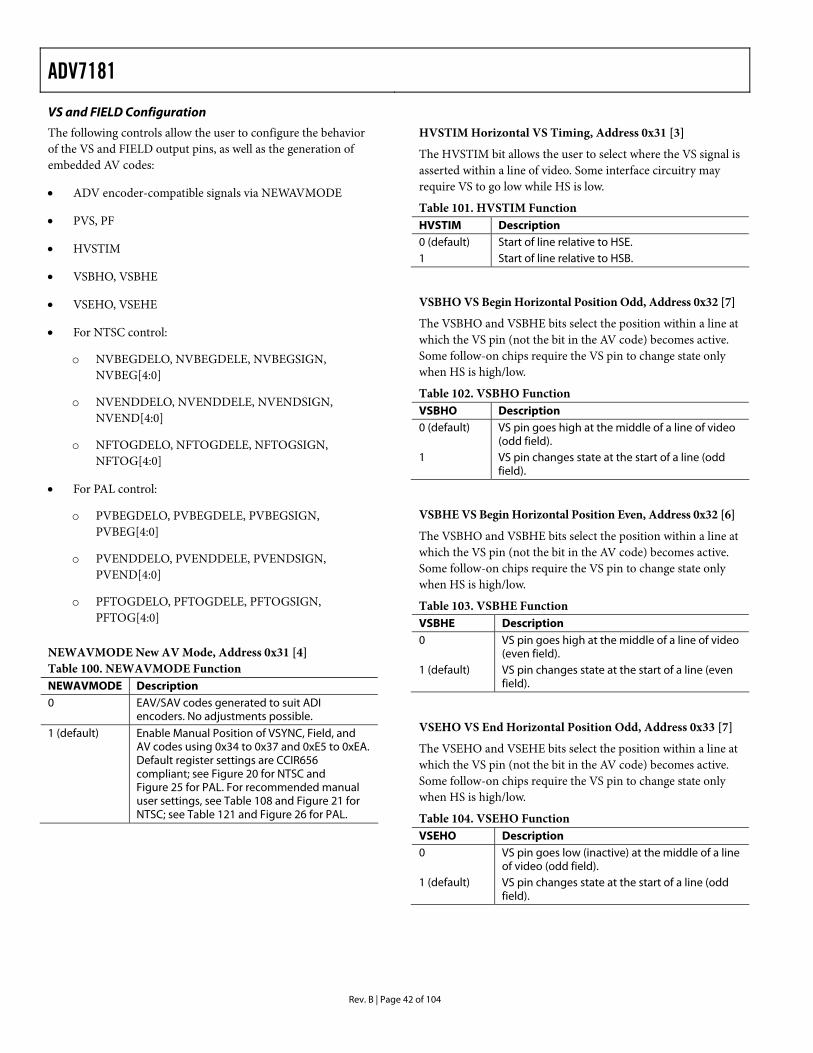
ADV7181
Rev. B | Page 42 of 104
VS and FIELD Configuration
The following controls allow the user to configure the behavior of the VS and FIELD output pins, as well as the generation of embedded AV codes:
• ADV encoder-compatible signals via NEWAVMODE
• PVS, PF
• HVSTIM
• VSBHO, VSBHE
• VSEHO, VSEHE
• For NTSC control:
o NVBEGDELO, NVBEGDELE, NVBEGSIGN, NVBEG[4:0]
o NVENDDELO, NVENDDELE, NVENDSIGN, NVEND[4:0]
o NFTOGDELO, NFTOGDELE, NFTOGSIGN, NFTOG[4:0]
• For PAL control:
o PVBEGDELO, PVBEGDELE, PVBEGSIGN, PVBEG[4:0]
o PVENDDELO, PVENDDELE, PVENDSIGN, PVEND[4:0]
o PFTOGDELO, PFTOGDELE, PFTOGSIGN, PFTOG[4:0]
NEWAVMODE New AV Mode, Address 0x31 [4] Table 100. NEWAVMODE Function NEWAVMODE Description 0 EAV/SAV codes generated to suit ADI
encoders. No adjustments possible. 1 (default) Enable Manual Position of VSYNC, Field, and
AV codes using 0x34 to 0x37 and 0xE5 to 0xEA. Default register settings are CCIR656 compliant; see Figure 20 for NTSC and Figure 25 for PAL. For recommended manual user settings, see Table 108 and Figure 21 for NTSC; see Table 121 and Figure 26 for PAL.
HVSTIM Horizontal VS Timing, Address 0x31 [3]
The HVSTIM bit allows the user to select where the VS signal is asserted within a line of video. Some interface circuitry may require VS to go low while HS is low.
Table 101. HVSTIM Function HVSTIM Description 0 (default) Start of line relative to HSE. 1 Start of line relative to HSB.
VSBHO VS Begin Horizontal Position Odd, Address 0x32 [7]
The VSBHO and VSBHE bits select the position within a line at which the VS pin (not the bit in the AV code) becomes active. Some follow-on chips require the VS pin to change state only when HS is high/low.
Table 102. VSBHO Function VSBHO Description 0 (default) VS pin goes high at the middle of a line of video
(odd field). 1 VS pin changes state at the start of a line (odd
field).
VSBHE VS Begin Horizontal Position Even, Address 0x32 [6]
The VSBHO and VSBHE bits select the position within a line at which the VS pin (not the bit in the AV code) becomes active. Some follow-on chips require the VS pin to change state only when HS is high/low.
Table 103. VSBHE Function VSBHE Description 0 VS pin goes high at the middle of a line of video
(even field). 1 (default) VS pin changes state at the start of a line (even
field).
VSEHO VS End Horizontal Position Odd, Address 0x33 [7]
The VSEHO and VSEHE bits select the position within a line at which the VS pin (not the bit in the AV code) becomes active. Some follow-on chips require the VS pin to change state only when HS is high/low.
Table 104. VSEHO Function VSEHO Description 0 VS pin goes low (inactive) at the middle of a line
of video (odd field). 1 (default) VS pin changes state at the start of a line (odd
field).
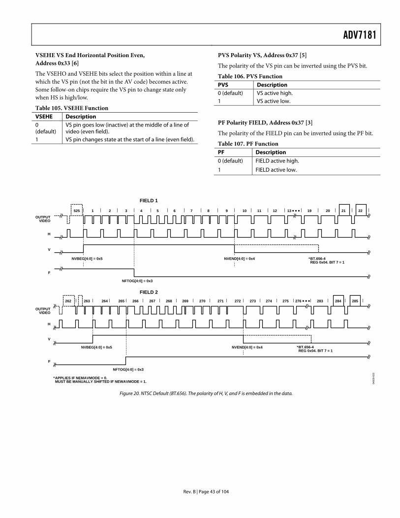
ADV7181
Rev. B | Page 43 of 104
VSEHE VS End Horizontal Position Even, Address 0x33 [6]
The VSEHO and VSEHE bits select the position within a line at which the VS pin (not the bit in the AV code) becomes active. Some follow-on chips require the VS pin to change state only when HS is high/low.
Table 105. VSEHE Function VSEHE Description 0 (default)
VS pin goes low (inactive) at the middle of a line of video (even field).
1 VS pin changes state at the start of a line (even field).
PVS Polarity VS, Address 0x37 [5]
The polarity of the VS pin can be inverted using the PVS bit.
Table 106. PVS Function PVS Description 0 (default) VS active high. 1 VS active low.
PF Polarity FIELD, Address 0x37 [3]
The polarity of the FIELD pin can be inverted using the PF bit.
Table 107. PF Function PF Description
0 (default) FIELD active high.
1 FIELD active low.
0482
0-02
0
OUTPUTVIDEO
FIELD 1
FIELD 2
H
V
F
OUTPUTVIDEO
H
V
F
525 1 2 3 4 5 6 7 8 9 10 11 12 13 19 20 21 22
NVBEG[4:0] = 0x5
NVBEG[4:0] = 0x5 NVEND[4:0] = 0x4
NVEND[4:0] = 0x4
NFTOG[4:0] = 0x3
NFTOG[4:0] = 0x3
*BT.656-4REG 0x04. BIT 7 = 1
*BT.656-4REG 0x04. BIT 7 = 1
*APPLIES IF NEMAVMODE = 0.MUST BE MANUALLY SHIFTED IF NEWAVMODE = 1.
262 263 264 265 266 267 268 269 270 271 272 273 274 275 276 283 284 285
Figure 20. NTSC Default (BT.656). The polarity of H, V, and F is embedded in the data.
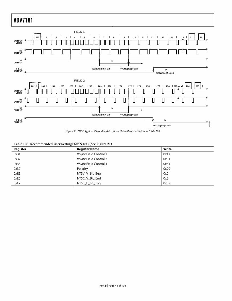
ADV7181
Rev. B | Page 44 of 104
NVBEG[4:0] = 0x0 NVEND[4:0] = 0x3
0482
0-02
1
FIELD 1
OUTPUTVIDEO
FIELDOUTPUT
HSOUTPUT
NFTOG[4:0] = 0x5
VSOUTPUT
525 1 2 3 4 5 6 7 8 9 10 11 12 13 14 15 21 22
FIELD 2
OUTPUTVIDEO
FIELDOUTPUT
HSOUTPUT
VSOUTPUT
262 263 264 265 266 267 268 269 270 271 272 273 274 275 276 277 284 285
NVBEG[4:0] = 0x0 NVEND[4:0] = 0x3
NFTOG[4:0] = 0x5
Figure 21. NTSC Typical VSync/Field Positions Using Register Writes in Table 108
Table 108. Recommended User Settings for NTSC (See Figure 21) Register Register Name Write
0x31 VSync Field Control 1 0x12
0x32 VSync Field Control 2 0x81 0x33 VSync Field Control 3 0x84
0x37 Polarity 0x29 0xE5 NTSV_V_Bit_Beg 0x0
0xE6 NTSC_V_Bit_End 0x3 0xE7 NTSC_F_Bit_Tog 0x85
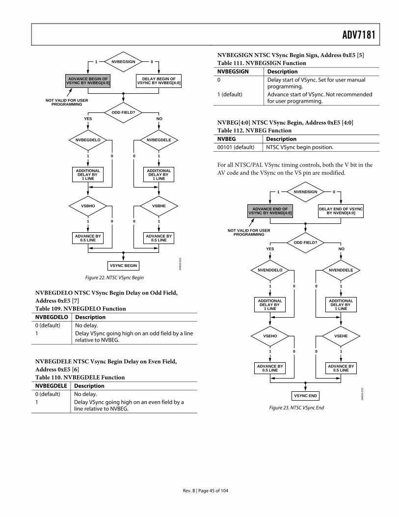
ADV7181
Rev. B | Page 45 of 104
0482
0-02
2
ADVANCE BEGIN OFVSYNC BY NVBEG[4:0]
DELAY BEGIN OFVSYNC BY NVBEG[4:0]
VSYNC BEGIN
NVBEGSIGN
ODD FIELD?
01
NOYES
NVBEGDELO
VSBHO
ADDITIONALDELAY BY
1 LINE
ADVANCE BY0.5 LINE
1 0
1 0
NVBEGDELE
VSBHE
ADDITIONALDELAY BY
1 LINE
ADVANCE BY0.5 LINE
10
10
NOT VALID FOR USERPROGRAMMING
Figure 22. NTSC VSync Begin
NVBEGDELO NTSC VSync Begin Delay on Odd Field, Address 0xE5 [7] Table 109. NVBEGDELO Function NVBEGDELO Description 0 (default) No delay. 1 Delay VSync going high on an odd field by a line
relative to NVBEG.
NVBEGDELE NTSC Vsync Begin Delay on Even Field, Address 0xE5 [6] Table 110. NVBEGDELE Function NVBEGDELE Description 0 (default) No delay. 1 Delay VSync going high on an even field by a
line relative to NVBEG.
NVBEGSIGN NTSC VSync Begin Sign, Address 0xE5 [5] Table 111. NVBEGSIGN Function NVBEGSIGN Description 0 Delay start of VSync. Set for user manual
programming. 1 (default) Advance start of VSync. Not recommended
for user programming.
NVBEG[4:0] NTSC VSync Begin, Address 0xE5 [4:0] Table 112. NVBEG Function NVBEG Description 00101 (default) NTSC VSync begin position.
For all NTSC/PAL VSync timing controls, both the V bit in the AV code and the VSync on the VS pin are modified.
0482
0-02
3
ADVANCE END OFVSYNC BY NVEND[4:0]
DELAY END OF VSYNCBY NVEND[4:0]
VSYNC END
NVENDSIGN
ODD FIELD?
01
NOYES
NVENDDELO
VSEHO
ADDITIONALDELAY BY
1 LINE
ADVANCE BY0.5 LINE
1 0
1 0
NVENDDELE
VSEHE
ADDITIONALDELAY BY
1 LINE
ADVANCE BY0.5 LINE
10
10
NOT VALID FOR USERPROGRAMMING
Figure 23. NTSC VSync End
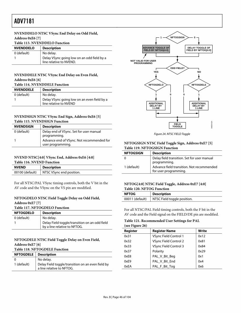
ADV7181
Rev. B | Page 46 of 104
NVENDDELO NTSC VSync End Delay on Odd Field, Address 0xE6 [7] Table 113. NVENDDELO Function NVENDDELO Description 0 (default) No delay. 1 Delay VSync going low on an odd field by a
line relative to NVEND.
NVENDDELE NTSC VSync End Delay on Even Field, Address 0xE6 [6] Table 114. NVENDDELE Function NVENDDELE Description 0 (default) No delay. 1 Delay VSync going low on an even field by a
line relative to NVEND
NVENDSIGN NTSC VSync End Sign, Address 0xE6 [5] Table 115. NVENDSIGN Function NVENDSIGN Description 0 (default) Delay end of VSync. Set for user manual
programming. 1 Advance end of VSync. Not recommended for
user programming.
NVEND NTSC[4:0] VSync End, Address 0xE6 [4:0] Table 116. NVEND Function NVEND Description 00100 (default) NTSC VSync end position.
For all NTSC/PAL VSync timing controls, both the V bit in the AV code and the VSync on the VS pin are modified.
NFTOGDELO NTSC Field Toggle Delay on Odd Field, Address 0xE7 [7] Table 117. NFTOGDELO Function NFTOGDELO Description 0 (default) No delay. 1 Delay Field toggle/transition on an odd field
by a line relative to NFTOG.
NFTOGDELE NTSC Field Toggle Delay on Even Field, Address 0xE7 [6] Table 118. NFTOGDELE Function NFTOGDELE Description 0 No delay. 1 (default) Delay Field toggle/transition on an even field by
a line relative to NFTOG.
0482
0-02
4
ADVANCE TOGGLE OFFIELD BY NFTOG[4:0]
DELAY TOGGLE OFFIELD BY NFTOG[4:0]
NFTOGSIGN
ODD FIELD?
01
NOYES
NFTOGDELE
ADDITIONALDELAY BY
1 LINE
10
NFTOGDELO
ADDITIONALDELAY BY
1 LINE
1 0
FIELDTOGGLE
NOT VALID FOR USERPROGRAMMING
Figure 24. NTSC FIELD Toggle
NFTOGSIGN NTSC Field Toggle Sign, Address 0xE7 [5] Table 119. NFTOGSIGN Function NFTOGSIGN Description 0 Delay field transition. Set for user manual
programming. 1 (default) Advance field transition. Not recommended
for user programming.
NFTOG[4:0] NTSC Field Toggle, Address 0xE7 [4:0] Table 120. NFTOG Function NFTOG Description 00011 (default) NTSC Field toggle position.
For all NTSC/PAL Field timing controls, both the F bit in the AV code and the Field signal on the FIELD/DE pin are modified.
Table 121. Recommended User Settings for PAL (see Figure 26) Register Register Name Write
0x31 VSync Field Control 1 0x12
0x32 VSync Field Control 2 0x81
0x33 VSync Field Control 3 0x84 0x37 Polarity 0x29
0xE8 PAL_V_Bit_Beg 0x1 0xE9 PAL_V_Bit_End 0x4
0xEA PAL_F_Bit_Tog 0x6
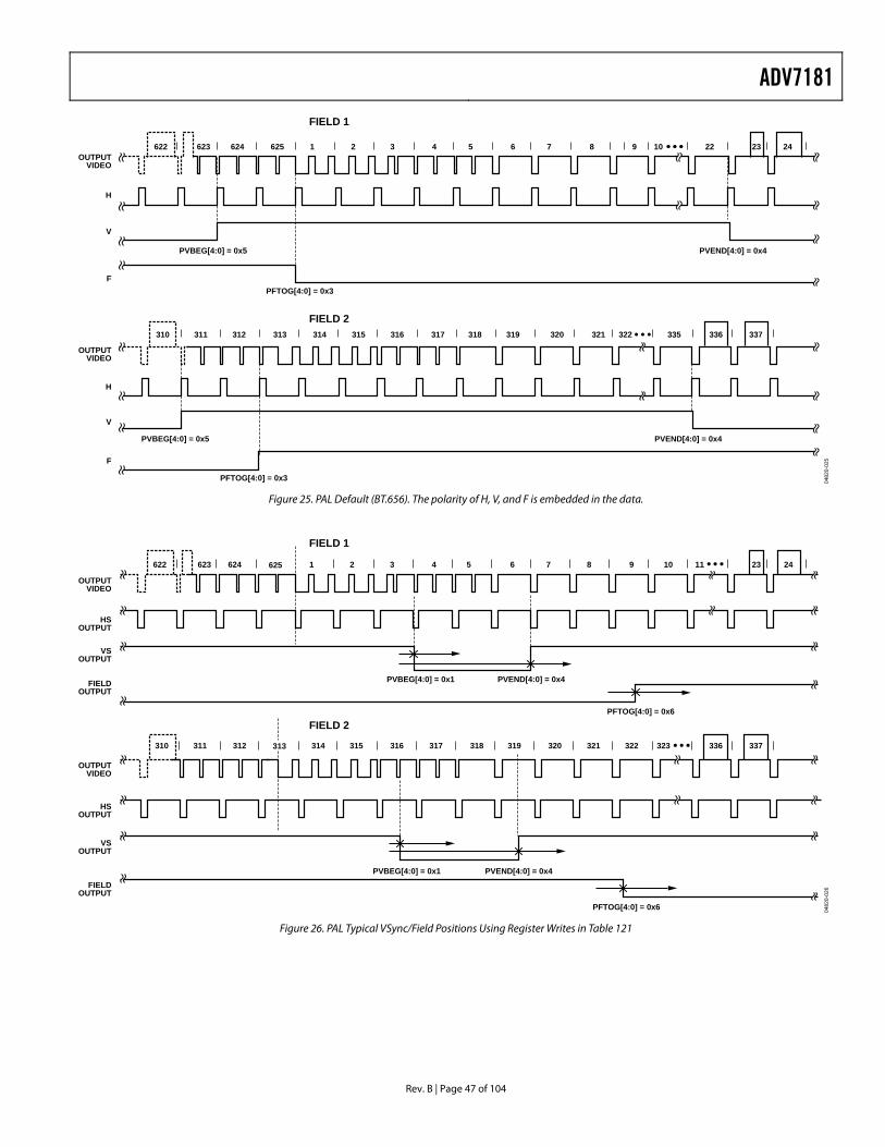
ADV7181
Rev. B | Page 47 of 104
0482
0-02
5
FIELD 1
OUTPUTVIDEO
H
V
F
622 623 624 625 1 2 3 4 5 6 7 8 9 10 22 23 24
PVBEG[4:0] = 0x5 PVEND[4:0] = 0x4
PFTOG[4:0] = 0x3
FIELD 2
OUTPUTVIDEO
H
V
F
PVBEG[4:0] = 0x5 PVEND[4:0] = 0x4
PFTOG[4:0] = 0x3
310 311 312 313 314 315 316 317 318 319 320 321 322 335 336 337
Figure 25. PAL Default (BT.656). The polarity of H, V, and F is embedded in the data.
0482
0-02
6
FIELD 1
622 623 624 625 1 2 3 4 5 6 7 8 9 10 11 23 24
310 311 312 313 314 315 316 317 318 319 320 321 322 323 336 337
PVBEG[4:0] = 0x1 PVEND[4:0] = 0x4
PFTOG[4:0] = 0x6
FIELD 2
OUTPUTVIDEO
FIELDOUTPUT
HSOUTPUT
VSOUTPUT
OUTPUTVIDEO
FIELDOUTPUT
HSOUTPUT
VSOUTPUT
PVBEG[4:0] = 0x1 PVEND[4:0] = 0x4
PFTOG[4:0] = 0x6
Figure 26. PAL Typical VSync/Field Positions Using Register Writes in Table 121
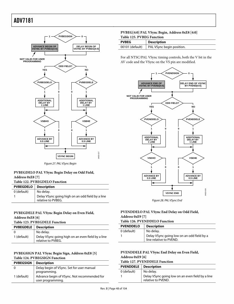
ADV7181
Rev. B | Page 48 of 104
0482
0-02
7
ADVANCE BEGIN OFVSYNC BY PVBEG[4:0]
DELAY BEGIN OFVSYNC BY PVBEG[4:0]
VSYNC BEGIN
PVBEGSIGN
ODD FIELD?
01
NOYES
PVBEGDELO
VSBHO
ADDITIONALDELAY BY
1 LINE
ADVANCE BY0.5 LINE
1 0
1 0
PVBEGDELE
VSBHE
ADDITIONALDELAY BY
1 LINE
ADVANCE BY0.5 LINE
10
10
NOT VALID FOR USERPROGRAMMING
Figure 27. PAL VSync Begin
PVBEGDELO PAL VSync Begin Delay on Odd Field, Address 0xE8 [7] Table 122. PVBEGDELO Function PVBEGDELO Description 0 (default) No delay. 1 Delay VSync going high on an odd field by a line
relative to PVBEG.
PVBEGDELE PAL VSync Begin Delay on Even Field, Address 0xE8 [6] Table 123. PVBEGDELE Function PVBEGDELE Description 0 No delay. 1 (default) Delay VSync going high on an even field by a line
relative to PVBEG.
PVBEGSIGN PAL VSync Begin Sign, Address 0xE8 [5] Table 124. PVBEGSIGN Function PVBEGSIGN Description 0 Delay begin of VSync. Set for user manual
programming. 1 (default) Advance begin of VSync. Not recommended for
user programming.
PVBEG[4:0] PAL VSync Begin, Address 0xE8 [4:0] Table 125. PVBEG Function PVBEG Description 00101 (default) PAL VSync begin position.
For all NTSC/PAL VSync timing controls, both the V bit in the AV code and the VSync on the VS pin are modified.
0482
0-02
8
ADVANCE END OFVSYNC BY PVEND[4:0]
DELAY END OF VSYNCBY PVEND[4:0]
VSYNC END
PVENDSIGN
ODD FIELD?
01
NOYES
PVENDDELO
VSEHO
ADDITIONALDELAY BY
1 LINE
ADVANCE BY0.5 LINE
1 0
1 0
PVENDDELE
VSEHE
ADDITIONALDELAY BY
1 LINE
ADVANCE BY0.5 LINE
10
10
NOT VALID FOR USERPROGRAMMING
Figure 28. PAL VSync End
PVENDDELO PAL VSync End Delay on Odd Field, Address 0xE9 [7] Table 126. PVENDDELO Function PVENDDELO Description 0 (default) No delay. 1 Delay VSync going low on an odd field by a
line relative to PVEND.
PVENDDELE PAL VSync End Delay on Even Field, Address 0xE9 [6] Table 127. PVENDDELE Function PVENDDELE Description 0 (default) No delay. 1 Delay VSync going low on an even field by a line
relative to PVEND.
ADV7181
Rev. B | Page 49 of 104
PVENDSIGN PAL VSync End Sign, Address 0xE9 [5] Table 128. PVENDSIGN Function PVENDSIGN Description 0 (default) Delay end of VSync. Set for user manual
programming. 1 Advance end of VSync. Not recommended
for user programming.
PVEND[4:0] PAL Vsync End, Address 0xE9,[4:0] Table 129. PVEND Function PVEND Description 10100 (default) PAL VSync end position.
For all NTSC/PAL VSync timing controls, both the V bit in the AV code and the VSync on the VS pin are modified.
PFTOGDELO PAL Field Toggle Delay on Odd Field, Address 0xEA [7] Table 130. PFTOGDELO Function PFTOGDELO Description 0 (default) No delay. 1 Delay F toggle/transition on an odd field by
a line relative to PFTOG.
PFTOGDELE PAL Field Toggle Delay on Even Field, Address 0xEA [6] Table 131. PFTOGDELE Function PFTOGDELE Description 0 No delay. 1 (default) Delay F toggle/transition on an even field by
a line relative to PFTOG.
PFTOGSIGN PAL Field Toggle Sign, Address 0xEA [5] Table 132. PFTOGSIGN Function PFTOGSIGN Description 0 Delay Field transition. Set for user manual
programming. 1 (default) Advance Field transition. Not recommended
for user programming.
PFTOG PAL Field Toggle, Address 0xEA [4:0] Table 133. PFTOG Function PFTOG Description 00011 (default) PAL Field toggle position.
For all NTSC/PAL Field timing controls, the F bit in the AV code and the Field signal on the FIELD/DE pin are modified.
0482
0-02
9
ADVANCE TOGGLE OFFIELD BY PTOG[4:0]
DELAY TOGGLE OFFIELD BY PFTOG[4:0]
PFTOGSIGN
ODD FIELD?
01
NOYES
PFTOGDELE
ADDITIONALDELAY BY
1 LINE
10
PFTOGDELO
ADDITIONALDELAY BY
1 LINE
1 0
FIELDTOGGLE
NOT VALID FOR USERPROGRAMMING
Figure 29. PAL F Toggle
SYNC PROCESSING The ADV7181 has two additional sync processing blocks that postprocess the raw synchronization information extracted from the digitized input video. If desired, the blocks can be disabled via the following two I2C bits.
ENHSPLL Enable HSync Processor, Address 0x01 [6]
The HSYNC processor is designed to filter incoming HSyncs that have been corrupted by noise, providing improved per-formance for video signals with stable time bases but poor SNR.
For CVBS PAL/NTSC, YC PAL/NTSC, enable the HSync processor. For SECAM, disable the HSync processor. For YPrPb signals, disable Hsync processor.
Table 134. ENHSPLL Function ENHSPLL Description 0 Disable the HSync processor. 1 (default) Enable the HSync processor.
ENVSPROC Enable VSync Processor, Address 0x01 [3]
This block provides extra filtering of the detected VSyncs to give improved vertical lock.
Table 135. ENVSPROC Function ENVSPROC Description 0 Disable VSync processor. 1 (default) Enable VSync processor.
ADV7181
Rev. B | Page 50 of 104
VBI DATA DECODE The following low data rate VBI signals can be decoded by the ADV7181:
• Wide screen signaling (WSS)
• Copy generation management systems (CGMS)
• Closed captioning (CCAP)
• EDTV
• Gemstar 1×- and 2×-compatible data recovery
The presence of any of the above signals is detected and, if applicable, a parity check is performed. The result of this testing is contained in a confidence bit in the VBI Info[7:0] register. Users are encouraged to first examine the VBI Info register before reading the corresponding data registers. All VBI data decode bits are read-only.
All VBI data registers are double-buffered with the field signals. This means that data is extracted from the video lines and appears in the appropriate I2C registers with the next field transition. They are then static until the next field.
The user should start an I2C read sequence with VS by first examining the VBI Info register. Then, depending on the data detected, the appropriate data registers should be read.
The data registers are filled with decoded VBI data even if their corresponding detection bits are low; it is likely that bits within the decoded data stream are wrong.
Notes
• The closed captioning data (CCAP) is available in the I2C registers, and is also inserted into the output video data stream during horizontal blanking.
• The Gemstar-compatible data is not available in the I2C registers, and is inserted into the data stream only during horizontal blanking.
WSSD Wide Screen Signaling Detected, Address 0x90 [0]
Logic 1 for this bit indicates that the data in the WSS1 and WSS2 registers is valid.
The WSSD bit goes high if the rising edge of the start bit is detected within a time window, and if the polarity of the parity bit matches the data transmitted.
Table 136. WSSD Function WSSD Description 0 No WSS detected. Confidence in decoded data is low. 1 WSS detected. Confidence in decoded data is high.
CCAPD Closed Caption Detected, Address 0x90 [1]
Logic 1 for this bit indicates that the data in the CCAP1 and CCAP2 registers is valid.
The CCAPD bit goes high if the rising edge of the start bit is detected within a time window, and if the polarity of the parity bit matches the data transmitted.
Table 137. CCAPD Function CCAPD Description 0 No CCAP signals detected. Confidence in
decoded data is low. 1 CCAP sequence detected. Confidence in
decoded data is high.
EDTVD EDTV Sequence Detected, Address 0x90 [2]
Logic 1 for this bit indicates that the data in the EDTV1, 2, 3 registers is valid.
The EDTVD bit goes high if the rising edge of the start bit is detected within a time window, and if the polarity of the parity bit matches the data transmitted.
Table 138. EDTVD Function EDTVD Description 0 No EDTV sequence detected. Confidence in
decoded data is low. 1 EDTV sequence detected. Confidence in
decoded data is high.
CGMSD CGMS-A Sequence Detected, Address 0x90 [3]
Logic 1 for this bit indicates that the data in the CGMS1, 2, 3 registers is valid. The CGMSD bit goes high if a valid CRC checksum has been calculated from a received CGMS packet.
Table 139. CGMSD Function CGMSD Description 0 No CGMS transmission detected, confidence
low. 1 CGMS sequence decoded, confidence high.
CRC_ENABLE CRC CGMS-A Sequence, Address 0xB2 [2]
For certain video sources, the CRC data bits may have an invalid format. In such circumstances, the CRC checksum validation procedure can be disabled. The CGMSD bit goes high if the rising edge of the start bit is detected within a time window.
Table 140. CRC_ENABLE Function CRC_ENABLE Description 0 No CRC check performed. The CGMSD bit goes
high if the rising edge of the start bit is detected within a time window.
1 (default) Use CRC checksum to validate the CGMS-A sequence. The CGMSD bit goes high for a valid checksum. ADI recommended setting.
ADV7181
Rev. B | Page 51 of 104
Wide Screen Signaling Data
WSS1[7:0], Address 0x91 [7:0], WSS2[7:0], Address 0x92 [7:0]
Figure 30 shows the bit correspondence between the analog video waveform and the WSS1/WSS2 registers. WSS2[7:6] are undetermined and should be masked out by software.
EDTV Data Registers
EDTV1[7:0], Address 0x93 [7:0], EDTV2[7:0], Address 0x94 [7:0], EDTV3[7:0], Address 0x95 [7:0]
Figure 31 shows the bit correspondence between the analog video waveform and the EDTV1/EDTV2/EDTV3 registers.
EDTV3[7:6] are undetermined and should be masked out by software. EDTV3[5] is reserved for future use and, for now, contains a 0. The three LSBs of the EDTV waveform are currently not supported.
0482
0-03
0
ACTIVEVIDEO
WSS2[5:0]WSS1[7:0]
RUN-INSEQUENCE
STARTCODE
0 1 2 3 4 5 6 7 0 1 2 3 4 5
11.0µs38.4µs42.5µs
Figure 30. WSS Data Extraction
Table 141. WSS Access Information Signal Name Register Location Address Register Default Value WSS1 [7:0] WSS 1 [7:0] 145d 0x91 Readback Only WSS2 [5:0] WSS 2 [5:0] 146d 0x92 Readback Only
EDTV1[7:0] EDTV2[7:0] EDTV3[5:0]
NOT SUPPORTED
0 1
3 4 5 6 7 0 1 2 3 4 5 6 7 0 1 2 3 4 5
2
0482
0-03
1
Figure 31. EDTV Data Extraction
Table 142. EDTV Access Information Signal Name Register Location Address Register Default Value EDTV1[7:0] EDTV 1 [7:0] 147d 0x93 Readback Only EDTV2[7:0] EDTV 2 [7:0] 148d 0x94 Readback Only EDTV3[7:0] EDTV 3 [7:0] 149d 0x95 Readback Only
ADV7181
Rev. B | Page 52 of 104
CGMS Data Registers
CGMS1[7:0], Address 0x96 [7:0], CGMS2[7:0], Address 0x97 [7:0], CGMS3[7:0], Address 0x98 [7:0]
Figure 32 shows the bit correspondence between the analog video waveform and the CGMS1/CGMS2/CGMS3 registers. CGMS3[7:4] are undetermined and should be masked out by software.
Closed Caption Data Registers
CCAP1[7:0], Address 0x99 [7:0], CCAP2[7:0], Address 0x9A [7:0]
Figure 33 shows the bit correspondence between the analog video waveform and the CCAP1/CCAP2 registers.
Notes
• CCAP1[7] contains the parity bit from the first word. CCAP2[7] contains the parity bit from the second word.
• Refer to the GDECAD Gemstar Decode Ancillary Data Format, Address 0x4C [0] section.
0482
0-03
2
0 1 2 3 4 5 6 7 0 1 2 3 4 5 6 7 0 1 2 3
CGMS2[7:0] CGMS3[3:0]CGMS1[7:0]REF
+100 IRE
+70 IRE
0 IRE
–40 IRE 11.2µs49.1µs ± 0.5µs
CRC SEQUENCE2.235µs ± 20ns
Figure 32. CGMS Data Extraction
Table 143. CGMS Access Information Signal Name Register Location Address Register Default Value CGMS1[7:0] CGMS 1 [7:0] 150d 0x96 Readback Only CGMS2[7:0] CGMS 2 [7:0] 151d 0x97 Readback Only CGMS3[3:0] CGMS 3 [3:0] 152d 0x98 Readback Only
0
REFERENCE COLOR BURST(9 CYCLES)
FREQUENCY = FSC = 3.579545MHzAMPLITUDE = 40 IRE
1
CCAP1[7:0]7 CYCLES
OF 0.5035MHz(CLOCK RUN-IN) CCAP2[7:0]
2 3 4 5 6 7 0 1 2 3 4 5 6 7PARITY
START
PARITY
BYTE 1BYTE 0
33.764µs10.003µs
10.5 ± 0.25µs 12.91µs
27.382µs
50 IRE
40 IRE
0482
0-03
3
Figure 33. Closed Caption Data Extraction
Table 144. CCAP Access Information Signal Name Register Location Address Register Default Value CCAP1[7:0] CCAP 1 [7:0] 153d 0x99 Readback Only CCAP2[7:0] CCAP 2 [7:0] 154d 0x9A Readback Only
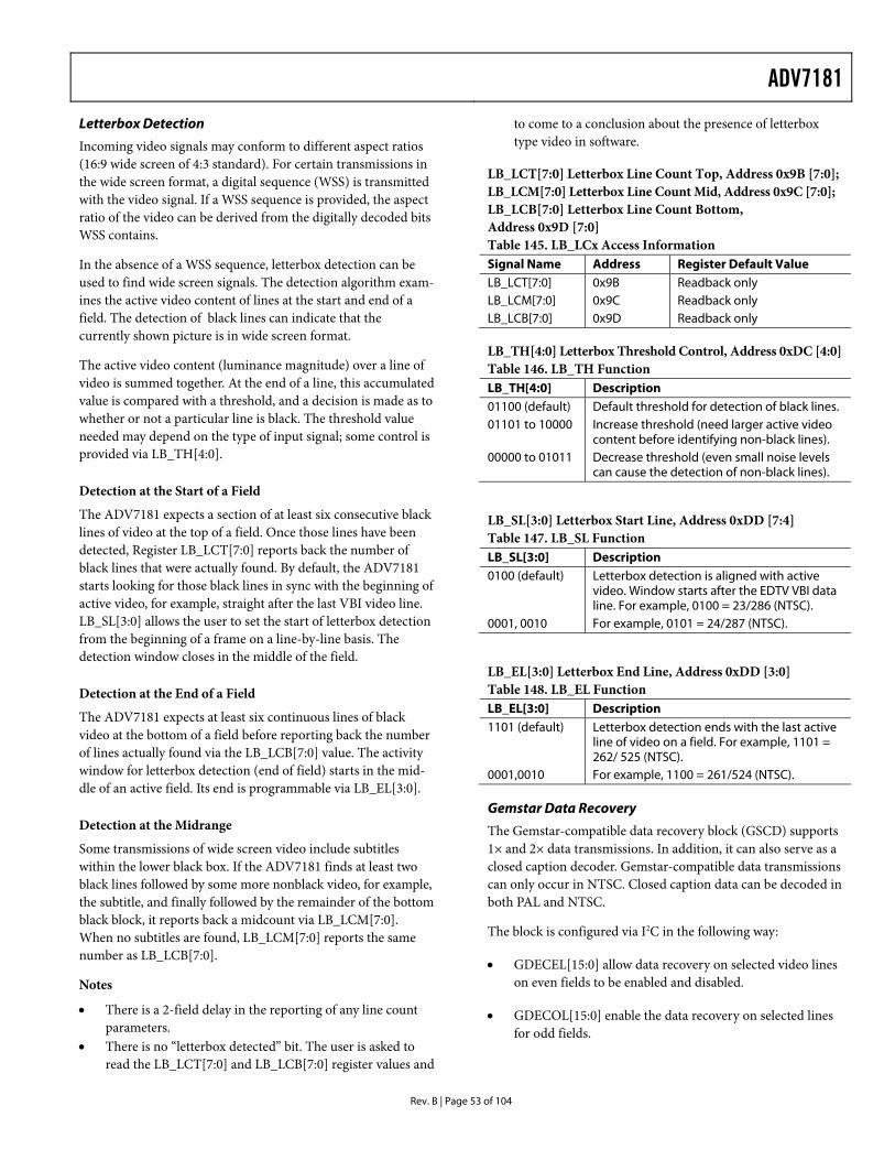
ADV7181
Rev. B | Page 53 of 104
Letterbox Detection
Incoming video signals may conform to different aspect ratios (16:9 wide screen of 4:3 standard). For certain transmissions in the wide screen format, a digital sequence (WSS) is transmitted with the video signal. If a WSS sequence is provided, the aspect ratio of the video can be derived from the digitally decoded bits WSS contains.
In the absence of a WSS sequence, letterbox detection can be used to find wide screen signals. The detection algorithm exam-ines the active video content of lines at the start and end of a field. The detection of black lines can indicate that the currently shown picture is in wide screen format.
The active video content (luminance magnitude) over a line of video is summed together. At the end of a line, this accumulated value is compared with a threshold, and a decision is made as to whether or not a particular line is black. The threshold value needed may depend on the type of input signal; some control is provided via LB_TH[4:0].
Detection at the Start of a Field
The ADV7181 expects a section of at least six consecutive black lines of video at the top of a field. Once those lines have been detected, Register LB_LCT[7:0] reports back the number of black lines that were actually found. By default, the ADV7181 starts looking for those black lines in sync with the beginning of active video, for example, straight after the last VBI video line. LB_SL[3:0] allows the user to set the start of letterbox detection from the beginning of a frame on a line-by-line basis. The detection window closes in the middle of the field.
Detection at the End of a Field
The ADV7181 expects at least six continuous lines of black video at the bottom of a field before reporting back the number of lines actually found via the LB_LCB[7:0] value. The activity window for letterbox detection (end of field) starts in the mid-dle of an active field. Its end is programmable via LB_EL[3:0].
Detection at the Midrange
Some transmissions of wide screen video include subtitles within the lower black box. If the ADV7181 finds at least two black lines followed by some more nonblack video, for example, the subtitle, and finally followed by the remainder of the bottom black block, it reports back a midcount via LB_LCM[7:0]. When no subtitles are found, LB_LCM[7:0] reports the same number as LB_LCB[7:0].
Notes
• There is a 2-field delay in the reporting of any line count parameters.
• There is no “letterbox detected” bit. The user is asked to read the LB_LCT[7:0] and LB_LCB[7:0] register values and
to come to a conclusion about the presence of letterbox type video in software.
LB_LCT[7:0] Letterbox Line Count Top, Address 0x9B [7:0]; LB_LCM[7:0] Letterbox Line Count Mid, Address 0x9C [7:0]; LB_LCB[7:0] Letterbox Line Count Bottom, Address 0x9D [7:0] Table 145. LB_LCx Access Information Signal Name Address Register Default Value LB_LCT[7:0] 0x9B Readback only LB_LCM[7:0] 0x9C Readback only LB_LCB[7:0] 0x9D Readback only
LB_TH[4:0] Letterbox Threshold Control, Address 0xDC [4:0] Table 146. LB_TH Function LB_TH[4:0] Description 01100 (default) Default threshold for detection of black lines. 01101 to 10000 Increase threshold (need larger active video
content before identifying non-black lines). 00000 to 01011 Decrease threshold (even small noise levels
can cause the detection of non-black lines).
LB_SL[3:0] Letterbox Start Line, Address 0xDD [7:4] Table 147. LB_SL Function LB_SL[3:0] Description 0100 (default) Letterbox detection is aligned with active
video. Window starts after the EDTV VBI data line. For example, 0100 = 23/286 (NTSC).
0001, 0010 For example, 0101 = 24/287 (NTSC).
LB_EL[3:0] Letterbox End Line, Address 0xDD [3:0] Table 148. LB_EL Function LB_EL[3:0] Description 1101 (default) Letterbox detection ends with the last active
line of video on a field. For example, 1101 = 262/ 525 (NTSC).
0001,0010 For example, 1100 = 261/524 (NTSC).
Gemstar Data Recovery
The Gemstar-compatible data recovery block (GSCD) supports 1× and 2× data transmissions. In addition, it can also serve as a closed caption decoder. Gemstar-compatible data transmissions can only occur in NTSC. Closed caption data can be decoded in both PAL and NTSC.
The block is configured via I2C in the following way:
• GDECEL[15:0] allow data recovery on selected video lines on even fields to be enabled and disabled.
• GDECOL[15:0] enable the data recovery on selected lines for odd fields.
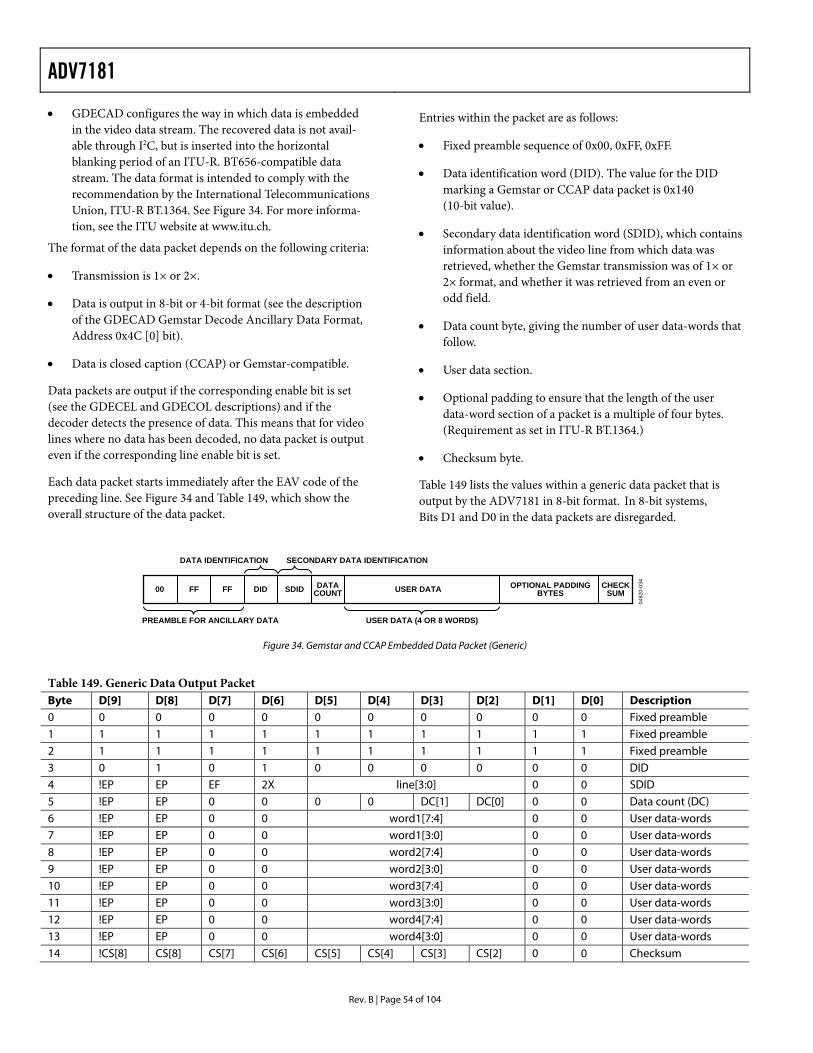
ADV7181
Rev. B | Page 54 of 104
• GDECAD configures the way in which data is embedded in the video data stream. The recovered data is not avail-able through I2C, but is inserted into the horizontal blanking period of an ITU-R. BT656-compatible data stream. The data format is intended to comply with the recommendation by the International Telecommunications Union, ITU-R BT.1364. See Figure 34. For more informa-tion, see the ITU website at www.itu.ch.
The format of the data packet depends on the following criteria:
• Transmission is 1× or 2×.
• Data is output in 8-bit or 4-bit format (see the description of the GDECAD Gemstar Decode Ancillary Data Format, Address 0x4C [0] bit).
• Data is closed caption (CCAP) or Gemstar-compatible.
Data packets are output if the corresponding enable bit is set (see the GDECEL and GDECOL descriptions) and if the decoder detects the presence of data. This means that for video lines where no data has been decoded, no data packet is output even if the corresponding line enable bit is set.
Each data packet starts immediately after the EAV code of the preceding line. See Figure 34 and Table 149, which show the overall structure of the data packet.
Entries within the packet are as follows:
• Fixed preamble sequence of 0x00, 0xFF, 0xFF.
• Data identification word (DID). The value for the DID marking a Gemstar or CCAP data packet is 0x140 (10-bit value).
• Secondary data identification word (SDID), which contains information about the video line from which data was retrieved, whether the Gemstar transmission was of 1× or 2× format, and whether it was retrieved from an even or odd field.
• Data count byte, giving the number of user data-words that follow.
• User data section.
• Optional padding to ensure that the length of the user data-word section of a packet is a multiple of four bytes. (Requirement as set in ITU-R BT.1364.)
• Checksum byte.
Table 149 lists the values within a generic data packet that is output by the ADV7181 in 8-bit format. In 8-bit systems, Bits D1 and D0 in the data packets are disregarded.
0482
0-03
4
00 FF FF DID SDID DATACOUNT USER DATA OPTIONAL PADDING
BYTESCHECK
SUM
SECONDARY DATA IDENTIFICATION
PREAMBLE FOR ANCILLARY DATA
DATA IDENTIFICATION
USER DATA (4 OR 8 WORDS)
Figure 34. Gemstar and CCAP Embedded Data Packet (Generic)
Table 149. Generic Data Output Packet Byte D[9] D[8] D[7] D[6] D[5] D[4] D[3] D[2] D[1] D[0] Description 0 0 0 0 0 0 0 0 0 0 0 Fixed preamble 1 1 1 1 1 1 1 1 1 1 1 Fixed preamble 2 1 1 1 1 1 1 1 1 1 1 Fixed preamble 3 0 1 0 1 0 0 0 0 0 0 DID 4 !EP EP EF 2X line[3:0] 0 0 SDID 5 !EP EP 0 0 0 0 DC[1] DC[0] 0 0 Data count (DC) 6 !EP EP 0 0 word1[7:4] 0 0 User data-words 7 !EP EP 0 0 word1[3:0] 0 0 User data-words 8 !EP EP 0 0 word2[7:4] 0 0 User data-words 9 !EP EP 0 0 word2[3:0] 0 0 User data-words 10 !EP EP 0 0 word3[7:4] 0 0 User data-words 11 !EP EP 0 0 word3[3:0] 0 0 User data-words 12 !EP EP 0 0 word4[7:4] 0 0 User data-words 13 !EP EP 0 0 word4[3:0] 0 0 User data-words 14 !CS[8] CS[8] CS[7] CS[6] CS[5] CS[4] CS[3] CS[2] 0 0 Checksum
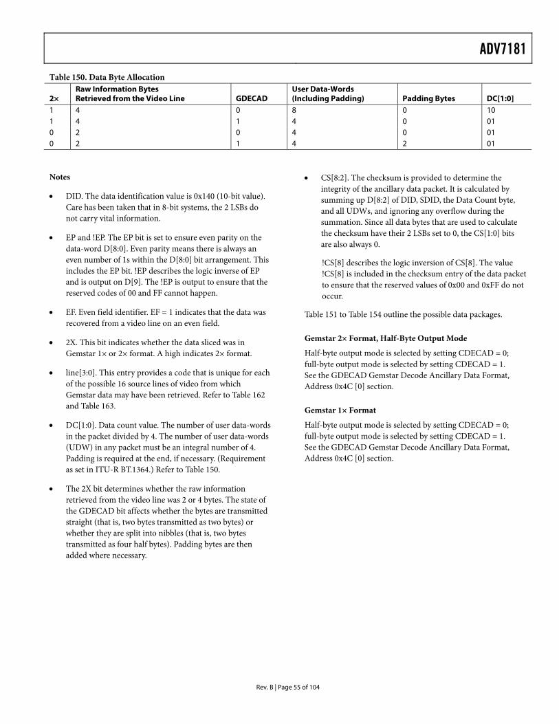
ADV7181
Rev. B | Page 55 of 104
Table 150. Data Byte Allocation
2× Raw Information Bytes Retrieved from the Video Line GDECAD
User Data-Words (Including Padding) Padding Bytes DC[1:0]
1 4 0 8 0 10 1 4 1 4 0 01 0 2 0 4 0 01 0 2 1 4 2 01
Notes
• DID. The data identification value is 0x140 (10-bit value). Care has been taken that in 8-bit systems, the 2 LSBs do not carry vital information.
• EP and !EP. The EP bit is set to ensure even parity on the data-word D[8:0]. Even parity means there is always an even number of 1s within the D[8:0] bit arrangement. This includes the EP bit. !EP describes the logic inverse of EP and is output on D[9]. The !EP is output to ensure that the reserved codes of 00 and FF cannot happen.
• EF. Even field identifier. EF = 1 indicates that the data was recovered from a video line on an even field.
• 2X. This bit indicates whether the data sliced was in Gemstar 1× or 2× format. A high indicates 2× format.
• line[3:0]. This entry provides a code that is unique for each of the possible 16 source lines of video from which Gemstar data may have been retrieved. Refer to Table 162 and Table 163.
• DC[1:0]. Data count value. The number of user data-words in the packet divided by 4. The number of user data-words (UDW) in any packet must be an integral number of 4. Padding is required at the end, if necessary. (Requirement as set in ITU-R BT.1364.) Refer to Table 150.
• The 2X bit determines whether the raw information retrieved from the video line was 2 or 4 bytes. The state of the GDECAD bit affects whether the bytes are transmitted straight (that is, two bytes transmitted as two bytes) or whether they are split into nibbles (that is, two bytes transmitted as four half bytes). Padding bytes are then added where necessary.
• CS[8:2]. The checksum is provided to determine the integrity of the ancillary data packet. It is calculated by summing up D[8:2] of DID, SDID, the Data Count byte, and all UDWs, and ignoring any overflow during the summation. Since all data bytes that are used to calculate the checksum have their 2 LSBs set to 0, the CS[1:0] bits are also always 0.
!CS[8] describes the logic inversion of CS[8]. The value !CS[8] is included in the checksum entry of the data packet to ensure that the reserved values of 0x00 and 0xFF do not occur.
Table 151 to Table 154 outline the possible data packages.
Gemstar 2× Format, Half-Byte Output Mode
Half-byte output mode is selected by setting CDECAD = 0; full-byte output mode is selected by setting CDECAD = 1. See the GDECAD Gemstar Decode Ancillary Data Format, Address 0x4C [0] section.
Gemstar 1× Format
Half-byte output mode is selected by setting CDECAD = 0; full-byte output mode is selected by setting CDECAD = 1. See the GDECAD Gemstar Decode Ancillary Data Format, Address 0x4C [0] section.
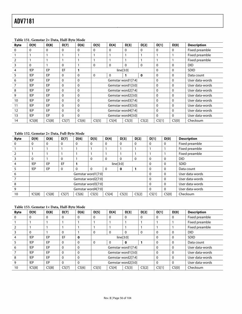
ADV7181
Rev. B | Page 56 of 104
Table 151. Gemstar 2× Data, Half-Byte Mode Byte D[9] D[8] D[7] D[6] D[5] D[4] D[3] D[2] D[1] D[0] Description 0 0 0 0 0 0 0 0 0 0 0 Fixed preamble 1 1 1 1 1 1 1 1 1 1 1 Fixed preamble 2 1 1 1 1 1 1 1 1 1 1 Fixed preamble 3 0 1 0 1 0 0 0 0 0 0 DID 4 !EP EP EF 1 line[3:0] 0 0 SDID
5 !EP EP 0 0 0 0 1 0 0 0 Data count
6 !EP EP 0 0 Gemstar word1[7:4] 0 0 User data-words 7 !EP EP 0 0 Gemstar word1[3:0] 0 0 User data-words 8 !EP EP 0 0 Gemstar word2[7:4] 0 0 User data-words 9 !EP EP 0 0 Gemstar word2[3:0] 0 0 User data-words 10 !EP EP 0 0 Gemstar word3[7:4] 0 0 User data-words 11 !EP EP 0 0 Gemstar word3[3:0] 0 0 User data-words 12 !EP EP 0 0 Gemstar word4[7:4] 0 0 User data-words 13 !EP EP 0 0 Gemstar word4[3:0] 0 0 User data-words 14 !CS[8] CS[8] CS[7] CS[6] CS[5] CS[4] CS[3] CS[2] CS[1] CS[0] Checksum
Table 152. Gemstar 2× Data, Full-Byte Mode Byte D[9] D[8] D[7] D[6] D[5] D[4] D[3] D[2] D[1] D[0] Description 0 0 0 0 0 0 0 0 0 0 0 Fixed preamble 1 1 1 1 1 1 1 1 1 1 1 Fixed preamble 2 1 1 1 1 1 1 1 1 1 1 Fixed preamble 3 0 1 0 1 0 0 0 0 0 0 DID 4 !EP EP EF 1 line[3:0] 0 0 SDID
5 !EP EP 0 0 0 0 0 1 0 0 Data count
6 Gemstar word1[7:0] 0 0 User data-words 7 Gemstar word2[7:0] 0 0 User data-words 8 Gemstar word3[7:0] 0 0 User data-words 9 Gemstar word4[7:0] 0 0 User data-words 10 !CS[8] CS[8] CS[7] CS[6] CS[5] CS[4] CS[3] CS[2] CS[1] CS[0] Checksum
Table 153. Gemstar 1× Data, Half-Byte Mode Byte D[9] D[8] D[7] D[6] D[5] D[4] D[3] D[2] D[1] D[0] Description 0 0 0 0 0 0 0 0 0 0 0 Fixed preamble 1 1 1 1 1 1 1 1 1 1 1 Fixed preamble 2 1 1 1 1 1 1 1 1 1 1 Fixed preamble 3 0 1 0 1 0 0 0 0 0 0 DID 4 !EP EP EF 0 line[3:0] 0 0 SDID
5 !EP EP 0 0 0 0 0 1 0 0 Data count
6 !EP EP 0 0 Gemstar word1[7:4] 0 0 User data-words 7 !EP EP 0 0 Gemstar word1[3:0] 0 0 User data-words 8 !EP EP 0 0 Gemstar word2[7:4] 0 0 User data-words 9 !EP EP 0 0 Gemstar word2[3:0] 0 0 User data-words 10 !CS[8] CS[8] CS[7] CS[6] CS[5] CS[4] CS[3] CS[2] CS[1] CS[0] Checksum
ADV7181
Rev. B | Page 57 of 104
Table 154. Gemstar 1× Data, Full-Byte Mode Byte D[9] D[8] D[7] D[6] D[5] D[4] D[3] D[2] D[1] D[0] Description 0 0 0 0 0 0 0 0 0 0 0 Fixed preamble 1 1 1 1 1 1 1 1 1 1 1 Fixed preamble 2 1 1 1 1 1 1 1 1 1 1 Fixed preamble 3 0 1 0 1 0 0 0 0 0 0 DID 4 !EP EP EF 0 line[3:0] 0 0 SDID
5 !EP EP 0 0 0 0 0 1 0 0 Data count
6 Gemstar word1[7:0] 0 0 User data-words 7 Gemstar word2[7:0] 0 0 User data-words 8 1 0 0 0 0 0 0 0 0 0 UDW padding 200h 9 1 0 0 0 0 0 0 0 0 0 UDW padding 200h 10 !CS[8] CS[8] CS[7] CS[6] CS[5] CS[4] CS[3] CS[2] CS[1] CS[0] Checksum
Table 155. NTSC CCAP Data, Half-Byte Mode Byte D[9] D[8] D[7] D[6] D[5] D[4] D[3] D[2] D[1] D[0] Description 0 0 0 0 0 0 0 0 0 0 0 Fixed preamble 1 1 1 1 1 1 1 1 1 1 1 Fixed preamble 2 1 1 1 1 1 1 1 1 1 1 Fixed preamble 3 0 1 0 1 0 0 0 0 0 0 DID 4 !EP EP EF 0 1 0 1 1 0 0 SDID
5 !EP EP 0 0 0 0 0 1 0 0 Data count
6 !EP EP 0 0 CCAP word1[7:4] 0 0 User data-words 7 !EP EP 0 0 CCAP word1[3:0] 0 0 User data-words 8 !EP EP 0 0 CCAP word2[7:4] 0 0 User data-words 9 !EP EP 0 0 CCAP word2[3:0] 0 0 User data-words 10 !CS[8] CS[8] CS[7] CS[6] CS[5] CS[4] CS[3] CS[2] CS[1] CS[0] Checksum
Table 156. NTSC CCAP Data, Full-Byte Mode Byte D[9] D[8] D[7] D[6] D[5] D[4] D[3] D[2] D[1] D[0] Description 0 0 0 0 0 0 0 0 0 0 0 Fixed preamble 1 1 1 1 1 1 1 1 1 1 1 Fixed preamble 2 1 1 1 1 1 1 1 1 1 1 Fixed preamble 3 0 1 0 1 0 0 0 0 0 0 DID 4 !EP EP EF 0 1 0 1 1 0 0 SDID
5 !EP EP 0 0 0 0 0 1 0 0 Data count
6 CCAP word1[7:0] 0 0 User data-words 7 CCAP word2[7:0] 0 0 User data-words 8 1 0 0 0 0 0 0 0 0 0 UDW padding 200h 9 1 0 0 0 0 0 0 0 0 0 UDW padding 200h 10 !CS[8] CS[8] CS[7] CS[6] CS[5] CS[4] CS[3] CS[2] CS[1] CS[0] Checksum
NTSC CCAP Data
Half-byte output mode is selected by setting CDECAD = 0; the full-byte mode is enabled by CDECAD = 1. Refer to the GDECAD Gemstar Decode Ancillary Data Format, Address 0x4C [0] section. The data packet formats are shown in Table 155 and Table 156.
Notes
• NTSC closed caption data is sliced on line 21d on even and odd fields. The corresponding enable bit has to be set high. See the GDECEL[15:0] Gemstar Decoding Even Lines, Address 0x48 [7:0]; Address 0x49 [7:0] and GDECOL[15:0] Gemstar Decoding Odd Lines, Address 0x4A [7:0]; Address 0x4B [7:0] sections.
ADV7181
Rev. B | Page 58 of 104
PAL CCAP Data
Half-Byte output mode is selected by setting CDECAD = 0, full-byte output mode is selected by setting CDECAD = 1. See the GDECAD Gemstar Decode Ancillary Data Format, Address 0x4C [0] section. Table 157 and Table 158 list the bytes of the data packet.
Notes
• PAL closed caption data is sliced from Lines 22 and 335. The corresponding enable bits have to be set.
• See the GDECEL[15:0] Gemstar Decoding Even Lines, Address 0x48 [7:0]; Address 0x49 [7:0] and GDECOL[15:0] Gemstar Decoding Odd Lines, Address 0x4A [7:0]; Address 0x4B [7:0] sections.
Table 157. PAL CCAP Data, Half-Byte Mode Byte D[9] D[8] D[7] D[6] D[5] D[4] D[3] D[2] D[1] D[0] Description 0 0 0 0 0 0 0 0 0 0 0 Fixed preamble 1 1 1 1 1 1 1 1 1 1 1 Fixed preamble 2 1 1 1 1 1 1 1 1 1 1 Fixed preamble 3 0 1 0 1 0 0 0 0 0 0 DID 4 !EP EP EF 0 1 0 1 0 0 0 SDID
5 !EP EP 0 0 0 0 0 1 0 0 Data count
6 !EP EP 0 0 CCAP word1[7:4] 0 0 User data-words 7 !EP EP 0 0 CCAP word1[3:0] 0 0 User data-words 8 !EP EP 0 0 CCAP word2[7:4] 0 0 User data-words 9 !EP EP 0 0 CCAP word2[3:0] 0 0 User data-words 10 !CS[8] CS[8] CS[7] CS[6] CS[5] CS[4] CS[3] CS[2] CS[1] CS[0] Checksum
Table 158. PAL CCAP Data, Full-Byte Mode Byte D[9] D[8] D[7] D[6] D[5] D[4] D[3] D[2] D[1] D[0] Description 0 0 0 0 0 0 0 0 0 0 0 Fixed preamble 1 1 1 1 1 1 1 1 1 1 1 Fixed preamble 2 1 1 1 1 1 1 1 1 1 1 Fixed preamble 3 0 1 0 1 0 0 0 0 0 0 DID 4 !EP EP EF 0 1 0 1 0 0 0 SDID
5 !EP EP 0 0 0 0 0 1 0 0 Data Count
6 CCAP word1[7:0] 0 0 User data-words 7 CCAP word2[7:0] 0 0 User data-words 8 1 0 0 0 0 0 0 0 0 0 UDW padding 200h 9 1 0 0 0 0 0 0 0 0 0 UDW padding 200h 10 !CS[8] CS[8] CS[7] CS[6] CS[5] CS[4] CS[3] CS[2] CS[1] CS[0] Checksum
ADV7181
Rev. B | Page 59 of 104
GDECEL[15:0] Gemstar Decoding Even Lines, Address 0x48 [7:0]; Address 0x49 [7:0]
The 16 bits of the GDECEL[15:0] are interpreted as a collection of 16 individual line decode enable signals. Each bit refers to a line of video in an even field. Setting the bit enables the decoder block trying to find Gemstar- or closed caption-compatible data on that particular line. Setting the bit to 0 prevents the decoder from trying to retrieve data. See Table 162 and Table 163.
Notes
• To retrieve closed caption data services on NTSC (Line 284), GDECEL[11] must be set.
• To retrieve closed caption data services on PAL (Line 335), GDECEL[14] must be set.
Table 159. GDECEL Function GDECEL[15:0] Description 0x0000 (default) Do not attempt to decode Gemstar-
compatible data or CCAP on any line (even field).
GDECOL[15:0] Gemstar Decoding Odd Lines, Address 0x4A [7:0]; Address 0x4B [7:0]
The 16 bits of the GDECOL[15:0] form a collection of 16 individual line decode enable signals. See Table 162 and Table 163.
Notes
• To retrieve closed caption data services on NTSC (Line 21), GDECOL[11] must be set.
• To retrieve closed caption data services on PAL (Line 22), GDECOL[14] must be set.
Table 160. GDECOL Function GDECOL[15:0] Description 0x0000 (default) Do not attempt to decode Gemstar-
compatible data or CCAP on any line (odd field).
GDECAD Gemstar Decode Ancillary Data Format, Address 0x4C [0]
The decoded data from Gemstar-compatible transmissions or closed caption is inserted into the horizontal blanking period of the respective line of video. There is a potential problem if the retrieved data bytes have the value 0x00 or 0xFF. In an ITU-R BT.656-compatible data stream, those values are reserved and used only to form a fixed preamble.
The GDECAD bit allows the data to be inserted into the horizontal blanking period in two ways:
• Insert all data straight into the data stream, even the reserved values of 0x00 and 0xFF, if they occur. This may violate the output data format specification ITU-R BT.1364.
• Split all data into nibbles and insert the half-bytes over double the number of cycles in a 4-bit format.
Table 161. GDECAD Function GDECAD Description 0 (default) Split data into half-bytes and insert. 1 Output data straight in 8-bit format.
ADV7181
Rev. B | Page 60 of 104
Table 162. NTSC Line Enable Bits and Corresponding Line Numbering
line[3:0] Line Number (ITU-R BT.470) Enable Bit Comment
0 10 GDECOL[0] Gemstar 1 11 GDECOL[1] Gemstar 2 12 GDECOL[2] Gemstar 3 13 GDECOL[3] Gemstar 4 14 GDECOL[4] Gemstar 5 15 GDECOL[5] Gemstar 6 16 GDECOL[6] Gemstar 7 17 GDECOL[7] Gemstar 8 18 GDECOL[8] Gemstar 9 19 GDECOL[9] Gemstar 10 20 GDECOL[10] Gemstar 11 21 GDECOL[11] Gemstar or
closed caption 12 22 GDECOL[12] Gemstar 13 23 GDECOL[13] Gemstar 14 24 GDECOL[14] Gemstar 15 25 GDECOL[15] Gemstar 0 273 (10) GDECEL[0] Gemstar 1 274 (11) GDECEL[1] Gemstar 2 275 (12) GDECEL[2] Gemstar 3 276 (13) GDECEL[3] Gemstar 4 277 (14) GDECEL[4] Gemstar 5 278 (15) GDECEL[5] Gemstar 6 279 (16) GDECEL[6] Gemstar 7 280 (17) GDECEL[7] Gemstar 8 281 (18) GDECEL[8] Gemstar 9 282 (19) GDECEL[9] Gemstar 10 283 (20) GDECEL[10] Gemstar 11 284 (21) GDECEL[11] Gemstar or
closed caption 12 285 (22) GDECEL[12] Gemstar 13 286 (23) GDECEL[13] Gemstar 14 287 (24) GDECEL[14] Gemstar 15 288 (25) GDECEL[15] Gemstar
Table 163. PAL Line Enable Bits and Corresponding Line Numbering
line[3:0] Line Number (ITU-R BT.470) Enable Bit Comment
12 8 GDECOL[0] Not valid 13 9 GDECOL[1] Not valid 14 10 GDECOL[2] Not valid 15 11 GDECOL[3] Not valid 0 12 GDECOL[4] Not valid 1 13 GDECOL[5] Not valid 2 14 GDECOL[6] Not valid 3 15 GDECOL[7] Not valid 4 16 GDECOL[8] Not valid 5 17 GDECOL[9] Not valid 6 18 GDECOL[10] Not valid 7 19 GDECOL[11] Not valid 8 20 GDECOL[12] Not valid 9 21 GDECOL[13] Not valid 10 22 GDECOL[14] Closed caption 11 23 GDECOL[15] Not valid 12 321 (8) GDECEL[0] Not valid 13 322 (9) GDECEL[1] Not valid 14 323 (10) GDECEL[2] Not valid 15 324 (11) GDECEL[3] Not valid 0 325 (12) GDECEL[4] Not valid 1 326 (13) GDECEL[5] Not valid 2 327 (14) GDECEL[6] Not valid 3 328 (15) GDECEL[7] Not valid 4 329 (16) GDECEL[8] Not valid 5 330 (17) GDECEL[9] Not valid 6 331 (18) GDECEL[10] Not valid 7 332 (19) GDECEL[11] Not valid 8 333 (20) GDECEL[12] Not valid 9 334 (21) GDECEL[13] Not valid 10 335 (22) GDECEL[14] Closed caption 11 336 (23) GDECEL[15] Not valid
ADV7181
Rev. B | Page 61 of 104
PIXEL PORT CONFIGURATION The ADV7181 has a very flexible pixel port that can be config-ured in a variety of formats to accommodate downstream ICs. Table 166 and Table 167 summarize the various functions that the ADV7181’s pins can have in different modes of operation.
The ordering of components, for example, Cr vs. Cb, CHA/B/C, can be changed. Refer to the SWPC Swap Pixel Cr/Cb, Address 0x27 [7] section. Table 166 indicates the default positions for the Cr/Cb components.
OF_SEL[3:0] Output Format Selection, Address 0x03 [5:2]
There are several modes in which the ADV7181 pixel port can be configured. These modes are under the control of OF_SEL[3:0]. See Table 167 for details.
The default LLC frequency output on the LLC1 pin is approxi-mately 27 MHz. For modes that operate with a nominal data rate of 13.5 MHz (0001, 0010), the clock frequency on the LLC1 pin stays at the higher rate of 27 MHz. For information on outputting the nominal 13.5 MHz clock on the LLC1 pin, see the LLC1 Output Selection, LLC_PAD_SEL[2:0], Address 0x8F [6:4] section.
SWPC Swap Pixel Cr/Cb, Address 0x27 [7]
This bit allows Cr and Cb samples to be swapped.
Table 164. SWPC Function SWPC Description 0 (default) No swapping. 1 Swap Cr and Cb values.
LLC1 Output Selection, LLC_PAD_SEL[2:0], Address 0x8F [6:4]
The following I2C write allows the user to select between the LLC1 (nominally at 27 MHz) and LLC2 (nominally at 13.5 MHz).
The LLC2 signal is useful for LLC2-compatible wide bus (16-bit) output modes. See the OF_SEL[3:0] Output Format Selection, Address 0x03 [5:2] section for additional information. The LLC2 signal and data on the data bus are synchronized. By default, the rising edge of LLC1/LLC2 is aligned with the Y data; the falling edge occurs when the data bus holds C data. The polarity of the clock, and therefore the Y/C assignments to the clock edges, can be altered by using the Polarity LLC pin.
Table 165. LLC_PAD_SEL Function LLC_PAD_SEL[2:0] Description 000 (default) Output nominal 27 MHz LLC on LLC1 pin. 101 Output nominal 13.5 MHz LLC on LLC1 pin.
Table 166. P15–P0 Output/Input Pin Mapping Data Port Pins P[15:0]
Processor, Format, and Mode 15 14 13 12 11 10 9 8 7 6 5 4 3 2 1 0 Video Out, 8-Bit, 4:2:2 YCrCb[7:0]OUT Video Out, 16-Bit, 4:2:2 Y[7:0]OUT CrCb[7:0] OUT
Table 167. Standard Definition Pixel Port Modes P[15: 0] OF_SEL[3:0] Format P[15:8] P[7: 0] 0010 16-Bit @ LLC2 4:2:2 Y[7:0] CrCb[7:0] 0011 (default) 8-Bit @ LLC1 4:2:2 YCrCb[7:0] Three-State 0110-1111 Reserved. Reserved. Do not use.
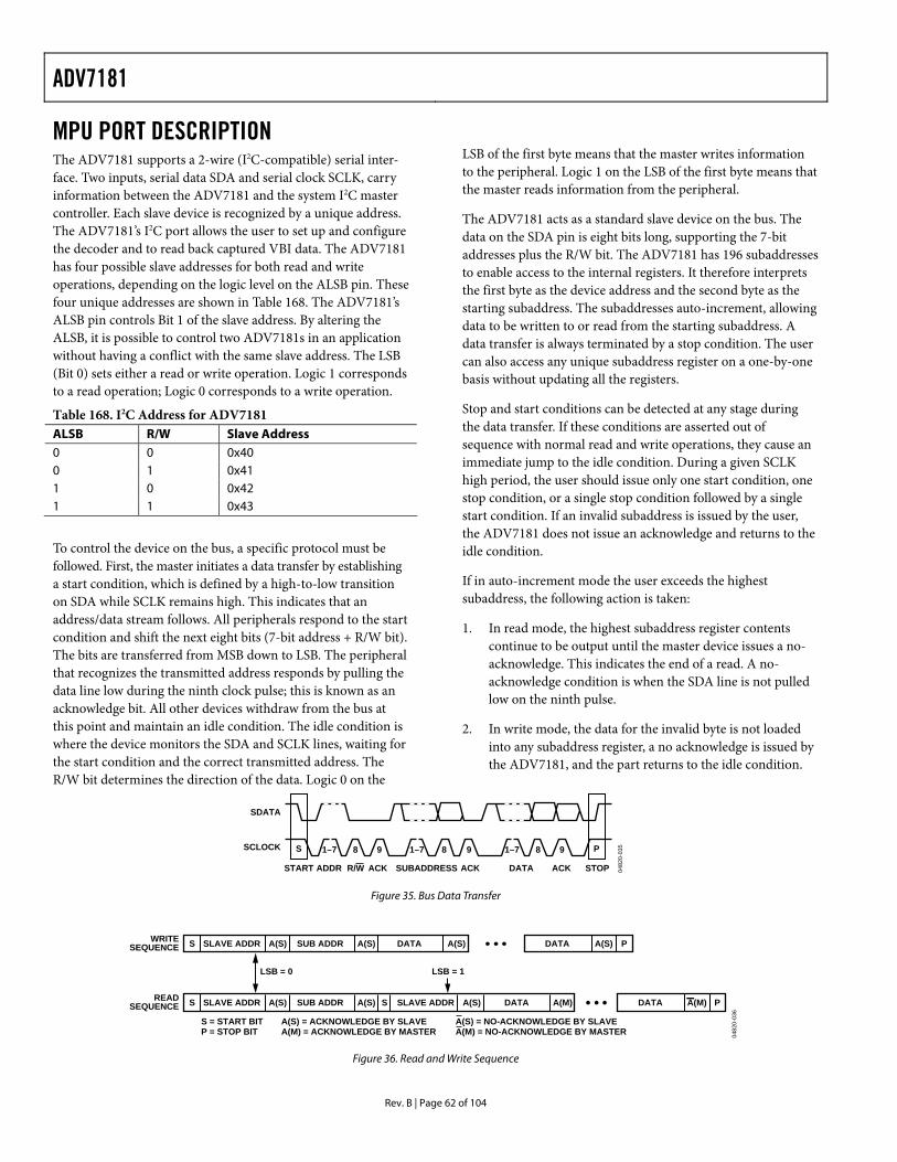
ADV7181
Rev. B | Page 62 of 104
MPU PORT DESCRIPTION The ADV7181 supports a 2-wire (I2C-compatible) serial inter-face. Two inputs, serial data SDA and serial clock SCLK, carry information between the ADV7181 and the system I2C master controller. Each slave device is recognized by a unique address. The ADV7181’s I2C port allows the user to set up and configure the decoder and to read back captured VBI data. The ADV7181 has four possible slave addresses for both read and write operations, depending on the logic level on the ALSB pin. These four unique addresses are shown in Table 168. The ADV7181’s ALSB pin controls Bit 1 of the slave address. By altering the ALSB, it is possible to control two ADV7181s in an application without having a conflict with the same slave address. The LSB (Bit 0) sets either a read or write operation. Logic 1 corresponds to a read operation; Logic 0 corresponds to a write operation.
Table 168. I2C Address for ADV7181 ALSB R/W Slave Address 0 0 0x40 0 1 0x41 1 0 0x42 1 1 0x43
To control the device on the bus, a specific protocol must be followed. First, the master initiates a data transfer by establishing a start condition, which is defined by a high-to-low transition on SDA while SCLK remains high. This indicates that an address/data stream follows. All peripherals respond to the start condition and shift the next eight bits (7-bit address + R/W bit). The bits are transferred from MSB down to LSB. The peripheral that recognizes the transmitted address responds by pulling the data line low during the ninth clock pulse; this is known as an acknowledge bit. All other devices withdraw from the bus at this point and maintain an idle condition. The idle condition is where the device monitors the SDA and SCLK lines, waiting for the start condition and the correct transmitted address. The R/W bit determines the direction of the data. Logic 0 on the
LSB of the first byte means that the master writes information to the peripheral. Logic 1 on the LSB of the first byte means that the master reads information from the peripheral.
The ADV7181 acts as a standard slave device on the bus. The data on the SDA pin is eight bits long, supporting the 7-bit addresses plus the R/W bit. The ADV7181 has 196 subaddresses to enable access to the internal registers. It therefore interprets the first byte as the device address and the second byte as the starting subaddress. The subaddresses auto-increment, allowing data to be written to or read from the starting subaddress. A data transfer is always terminated by a stop condition. The user can also access any unique subaddress register on a one-by-one basis without updating all the registers.
Stop and start conditions can be detected at any stage during the data transfer. If these conditions are asserted out of sequence with normal read and write operations, they cause an immediate jump to the idle condition. During a given SCLK high period, the user should issue only one start condition, one stop condition, or a single stop condition followed by a single start condition. If an invalid subaddress is issued by the user, the ADV7181 does not issue an acknowledge and returns to the idle condition.
If in auto-increment mode the user exceeds the highest subaddress, the following action is taken:
1. In read mode, the highest subaddress register contents continue to be output until the master device issues a no-acknowledge. This indicates the end of a read. A no-acknowledge condition is when the SDA line is not pulled low on the ninth pulse.
2. In write mode, the data for the invalid byte is not loaded into any subaddress register, a no acknowledge is issued by the ADV7181, and the part returns to the idle condition.
0482
0-03
5
SDATA
SCLOCK
START ADDR ACK ACK DATA ACK STOPSUBADDRESS
1–7 1–78 9 8 9 1–7 8 9S P
R/W
Figure 35. Bus Data Transfer
0482
0-03
6
SWRITESEQUENCE SLAVE ADDR A(S) SUB ADDR A(S) DATA A(S) DATA A(S) P
SREADSEQUENCE SLAVE ADDR SLAVE ADDRA(S) SUB ADDR A(S) S A(S) DATA A(M) DATA A(M) P
S = START BITP = STOP BIT
A(S) = ACKNOWLEDGE BY SLAVEA(M) = ACKNOWLEDGE BY MASTER
A(S) = NO-ACKNOWLEDGE BY SLAVEA(M) = NO-ACKNOWLEDGE BY MASTER
LSB = 1LSB = 0
Figure 36. Read and Write Sequence
ADV7181
Rev. B | Page 63 of 104
REGISTER ACCESSES The MPU can write to or read from all of the ADV7181’s registers, except those registers that are read-only or write-only. The Subaddress register determines which register the next read or write operation accesses. All communications with the part through the bus start with an access to the Subaddress register. Then a read/write operation is performed from/to the target address, which increments to the next address until a stop command on the bus is performed.
REGISTER PROGRAMMING The following sections describe each register in terms of its configuration. The Communications register is an 8-bit, write-only register. After the part has been accessed over the bus and a read/write operation is selected, the subaddress is set up. The Subaddress register determines to/from which register the operation takes place. Table 170 lists the various operations under the control of the Subaddress register for the control port.
Register Select (SR7-SR0)
These bits are set up to point to the required starting address.
I2C SEQUENCER An I2C sequencer is used when a parameter exceeds eight bits, and is therefore distributed over two or more I2C registers, for example, HSB [11:0].
When such a parameter is changed using two or more I2C write operations, the parameter may hold an invalid value for the time between the first I2C finishing and the last I2C being completed. In other words, the top bits of the parameter may already hold the new value while the remaining bits of the parameter still hold the previous value.
To avoid this problem, the I2C sequencer holds the already updated bits of the parameter in local memory; all bits of the parameter are updated together once the last register write operation has completed.
The correct operation of the I2C sequencer relies on the following:
• All I2C registers for the parameter in question must be written to in order of ascending addresses, for example, for HSB[10:0], write to Address 0x34 first, followed by 0x35.
• No other I2C taking place between the two (or more) I2C writes for the sequence, for example, for HSB[10:0], write to Address 0x34 first, immediately followed by 0x35.
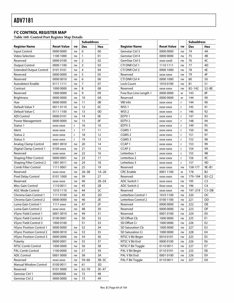
ADV7181
Rev. B | Page 64 of 104
I2C CONTROL REGISTER MAP Table 169. Control Port Register Map Details
Subaddress Register Name Reset Value rw Dec Hex Input Control 0000 0000 rw 0 00
Video Selection 1100 1000 rw 1 01
Reserved 0000 0100 rw 2 02
Output Control 0000 1100 rw 3 03
Extended Output Control 0101 0101 rw 4 04
Reserved 0000 0000 rw 5 05
Reserved 0000 0010 rw 6 06
Autodetect Enable 0111 1111 rw 7 07
Contrast 1000 0000 rw 8 08
Reserved 1000 0000 rw 9 09
Brightness 0000 0000 rw 10 0A
Hue 0000 0000 rw 11 0B
Default Value Y 0011 0110 rw 12 0C
Default Value C 0111 1100 rw 13 0D
ADI Control 0000 0101 rw 14 0E
Power Management 0000 0000 rw 15 0F
Status 1 xxxx xxxx r 16 10
Ident xxxx xxxx r 17 11
Status 2 xxxx xxxx r 18 12
Status 3 xxxx xxxx r 19 13
Analog Clamp Control 0001 0010 rw 20 14
Digital Clamp Control 1 0100 xxxx rw 21 15
Reserved xxxx xxxx rw 22 16
Shaping Filter Control 0000 0001 rw 23 17
Shaping Filter Control 2 1001 0011 rw 24 18
Comb Filter Control 1111 0001 rw 25 19
Reserved xxxx xxxx rw 26–38 1A–26
Pixel Delay Control 0101 1000 rw 39 27
Reserved xxxx xxxx rw 40 28–2A
Misc Gain Control 1110 0011 rw 43 2B
AGC Mode Control 1010 1110 rw 44 2C
Chroma Gain Control 1 1111 0100 rw 45 2D
Chroma Gain Control 2 0000 0000 rw 46 2E
Luma Gain Control 1 1111 xxxx rw 47 2F
Luma Gain Control 2 xxxx xxxx rw 48 30
VSync Field Control 1 0001 0010 rw 49 31
VSync Field Control 2 0100 0001 rw 50 32
VSync Field Control 3 1000 0100 51 33
HSync Position Control 1 0000 0000 rw 52 34
HSync Position Control 2 0000 0010 rw 53 35
HSync Position Control 3 0000 0000 rw 54 36
Polarity 0000 0001 rw 55 37
NTSC Comb Control 1000 0000 rw 56 38
PAL Comb Control 1100 0000 rw 57 39
ADC Control 0001 0000 rw 58 3A
Reserved xxxx xxxx rw 59–60 3B–3C
Manual Window Control 0100 0011 rw 61 3D
Reserved 0101 0000 rw 62–70 3E–47
Gemstar Ctrl 1 00000000 rw 72 48
Gemstar Ctrl 2 0000 0000 rw 73 49
Subaddress Register Name Reset Value rw Dec Hex Gemstar Ctrl 3 0000 0000 rw 74 4A
Gemstar Ctrl 4 0000 0000 rw 75 4B
GemStar Ctrl 5 xxxx xxx0 rw 76 4C
CTI DNR Ctrl 1 1110 1111 rw 77 4D
CTI DNR Ctrl 2 0000 1000 rw 78 4E
Reserved xxxx xxxx rw 79 4F
CTI DNR Ctrl 4 0000 1000 rw 80 50
Lock Count 1010 0100 rw 81 51
Reserved xxxx xxxx rw 82–142 52–8E
Free Run Line Length 1 0000 0000 w 143 8F
Reserved 0000 0000 w 144 90
VBI Info xxxx xxxx r 144 90
WSS 1 xxxx xxxx r 145 91
WSS 2 xxxx xxxx r 146 92
EDTV 1 xxxx xxxx r 147 93
EDTV 2 xxxx xxxx r 148 94
EDTV 3 xxxx xxxx r 149 95
CGMS 1 xxxx xxxx r 150 96
CGMS 2 xxxx xxxx r 151 97
CGMS 3 xxxx xxxx r 152 98
CCAP 1 xxxx xxxx r 153 99
CCAP 2 xxxx xxxx r 154 9A
Letterbox 1 xxxx xxxx r 155 9B
Letterbox 2 xxxx xxxx r 156 9C
Letterbox 3 xxxx xxxx r 157 9D
Reserved xxxx xxxx rw 158-177 9E–B1
CRC Enable 0001 1100 w 178 B2
Reserved xxxx xxxx rw 179–194 B2–C2
ADC Switch 1 xxxx xxxx rw 195 C3
ADC Switch 2 0xxx xxxx rw 196 C4
Reserved xxxx xxxx rw 197–219 C5–DB
Letterbox Control 1 1010 1100 rw 220 DC
Letterbox Control 2 0100 1100 rw 221 DD
Reserved 0000 0000 rw 222 DE
Reserved 0000 0000 rw 223 DF
Reserved 0001 0100 rw 224 E0
SD Offset Cb 1000 0000 rw 225 E1
SD Offset Cr 1000 0000 rw 226 E2
SD Saturation Cb 1000 0000 rw 227 E3
SD Saturation Cr 1000 0000 rw 228 E4
NTSC V Bit Begin 0010 0101 rw 225 E5
NTSC V Bit End 0000 0100 rw 226 E6
NTSC F Bit Toggle 0110 0011 rw 227 E7
PAL V Bit Begin 0110 0101 rw 225 E8
PAL V Bit End 0001 0100 rw 226 E9
PAL F Bit Toggle 0110 0011 rw 227 EA
ADV7181
Rev. B | Page 65 of 104
Table 170. Control Port Register Map Bit Details Register Name Bit 7 Bit 6 Bit 5 Bit 4 Bit 3 Bit 2 Bit 1 Bit 0
Input Control VID_SEL.3 VID_SEL.2 VID_SEL.1 VID_SEL.0 INSEL.3 INSEL.2 INSEL.1 INSEL.0
Video Selection ENHSPLL BETACAM ENVSPROC
Reserved
Output Control VBI_EN TOD OF_SEL.3 OF_SEL.2 OF_SEL.1 OF_SEL.0 SD_DUP_AV
Extended Output Control
BT656-4 DR_STR.1 DR_STR.0 TIM_OE BL_C_VBI EN_SFL_PI RANGE
Reserved
Reserved
Autodetect Enable AD_SEC525_EN AD_SECAM_EN AD_N443_EN AD_P60_EN AD_PALN_EN AD_PALM_EN AD_NTSC_EN AD_PAL_EN
Contrast CON.7 CON.6 CON.5 CON.4 CON.3 CON.2 CON.1 CON.0
Reserved
Brightness BRI.7 BRI.6 BRI.5 BRI.4 BRI.3 BRI.2 BRI.1 BRI.0
Hue HUE.7 HUE.6 HUE.5 HUE.4 HUE.3 HUE.2 HUE.1 HUE.0
Default Value Y DEF_Y.5 DEF_Y.4 DEF_Y.3 DEF_Y.2 DEF_Y.1 DEF_Y.0 DEF_VAL_AUTO_EN DEF_VAL_EN
Default Value C DEF_C.7 DEF_C.6 DEF_C.5 DEF_C.4 DEF_C.3 DEF_C.2 DEF_C.1 DEF_C.0
ADI Control TRI_LLC DR_STR_C.1 DR_STR_C.0 DR_STR_S.1 DR_STR_S.0
Power Management PWRDN PDBP
Status 1 COL_KILL AD_RESULT.2 AD_RESULT.1 AD_RESULT.0 FOLLOW_PW FSC_LOCK LOST_LOCK IN_LOCK
Ident IDENT.7 IDENT.6 IDENT.5 IDENT.4 IDENT.3 IDENT.2 IDENT.1 IDENT.0
Status 2 FSC NSTD LL NSTD MV AGC DET MV PS DET MVCS T3 MVCS DET
Status 3 PAL SW LOCK INTERLACE STD FLD LEN FREE_RUN_ACT INST_HLOC K
Analog Clamp Control
CCLEN
Digital Clamp Control 1
DCT.1 DCT.0
Reserved
Shaping Filter Control
CSFM.2 CSFM.1 CSFM.0 YSFM.4 YSFM.3 YSFM.2 YSFM.1 YSFM.0
Shaping Filter Control 2
WYSFMOVR WYSFM.4 WYSFM.3 WYSFM.2 WYSFM.1 WYSFM.0
Comb Filter Control NSFSEL.1 NSFSEL.0 PSFSEL.1 PSFSEL.0
Reserved
Pixel Delay Control SWPC AUTO_PDC_EN CTA.2 CTA.1 CTA.0 LTA.1 LTA.0
Reserved
Misc Gain Control CKE PW_UPD
AGC Mode Control LAGC.2 LAGC.1 LAGC.0 CAGC.1 CAGC.0
Chroma Gain Control 1
CAGT.1 CAGT.0 CMG.11 CMG.10 CMG.9 CMG.8
Chroma Gain Control 2
CMG.7 CMG.6 CMG.5 CMG.4 CMG.3 CMG.2 CMG.1 CMG.0
Luma Gain Control 1
LAGT.1 LGAT.0 LMG.11 LMG.10 LMG.9 LMG.8
Luma Gain Control 2
LMG.7 LMG.6 LMG.5 LMG.4 LMG.3 LMG.2 LMG.1 LMG.0
VSync Field Control 1
NEWAVMODE HVSTIM
VSync Field Control 2
VSBHO VSBHE
VSync Field Control 3
VSEHO VSEHE
HSync Position Control 1
HSB.10 HSB.9 HSB.8 HSE.10 HSE.9 HSE.8
HSync Position Control 2
HSB.7 HSB.6 HSB.5 HSB.4 HSB.3 HSB.2 HSB.1 HSB.0
HSync Position Control 3
HSE.7 HSE.6 HSE.5 HSE.4 HSE.3 HSE.2 HSE.1 HSE.0
Polarity PHS PVS PF PCLK
NTSC Comb Control CTAPSN.1 CTAPSN.0 CCMN.2 CCMN.1 CCMN.0 YCMN.2 YCMN.1 YCMN.0
PAL Comb Control CTAPSP.1 CTAPSP.0 CCMP.2 CCMP.1 CCMP.0 YCMP.2 YCMP.1 YCMP.0
ADC Control PWRDN_AD C_0 PWRDN_AD C_1 PWRDN_ADC_2
Reserved
Manual Window Control
CKILLTHR.2 CKILLTHR.1 CKILLTHR.0
Reserved
ADV7181
Rev. B | Page 66 of 104
Register Name Bit 7 Bit 6 Bit 5 Bit 4 Bit 3 Bit 2 Bit 1 Bit 0
Gemstar Ctrl 1 GDECEL.15 GDECEL.14 GDECEL.13 GDECEL.12 GDECEL.11 GDECEL.10 GDECEL.9 GDECEL.8
Gemstar Ctrl 2 GDECEL.7 GDECEL.6 GDECEL.5 GDECEL.4 GDECEL.3 GDECEL.2 GDECEL.1 GDECEL.0
Gemstar Ctrl 3 GDECOL.15 GDECOL.14 GDECOL.13 GDECOL.12 GDECOL.11 GDECOL.10 GDECOL.9 GDECOL.8
Gemstar Ctrl 4 GDECOL.7 GDECOL.6 GDECOL.5 GDECOL.4 GDECOL.3 GDECOL.2 GDECOL.1 GDECOL.0
Gemstar Ctrl 5 GDECAD
CTI DNR Ctrl 1 DNR_EN CTI_AB.1 CTI_AB.0 CTI_AB_EN CTI_EN
CTI DNR Ctrl 2 CTI_C_TH.7 CTI_C_TH.6 CTI_C_TH.5 CTI_C_TH.4 CTI_C_TH.3 CTI_C_TH.2 CTI_C_TH.1 CTI_C_TH.0
Reserved
CTI DNR Ctrl 4 DNR_TH.7 DNR_TH.6 DNR_TH.5 DNR_TH.4 DNR_TH.3 DNR_TH.2 DNR_TH.1 DNR_TH.0
Lock Count FSCLE SRLS COL.2 COL.1 COL.0 CIL.2 CIL.1 CIL.0
Reserved
Free Run Line Length 1
LLC_PAD_SEL.2 LLC_PAD_SEL.1 LLC_PAD_SEL.0
Reserved
VBI Info CGMSD EDTVD CCAPD WSSD
WSS 1 WSS1.7 WSS1.6 WSS1.5 WSS1.4 WSS1.3 WSS1.2 WSS1.1 WSS1.0
WSS 2 WSS2.7 WSS2.6 WSS2.5 WSS2.4 WSS2.3 WSS2.2 WSS2.1 WSS2.0
EDTV 1 EDTV1.7 EDTV1.6 EDTV1.5 EDTV1.4 EDTV1.3 EDTV1.2 EDTV1.1 EDTV1.0
EDTV 2 EDTV2.7 EDTV2.6 EDTV2.5 EDTV2.4 EDTV2.3 EDTV2.2 EDTV2.1 EDTV2.0
EDTV 3 EDTV3.7 EDTV3.6 EDTV3.5 EDTV3.4 EDTV3.3 EDTV3.2 EDTV3.1 EDTV3.0
CGMS 1 CGMS1.7 CGMS1.6 CGMS1.5 CGMS1.4 CGMS1.3 CGMS1.2 CGMS1.1 CGMS1.0
CGMS 2 CGMS2.7 CGMS2.6 CGMS2.5 CGMS2.4 CGMS2.3 CGMS2.2 CGMS2.1 CGMS2.0
CGMS 3 CGMS3.7 CGMS3.6 CGMS3.5 CGMS3.4 CGMS3.3 CGMS3.2 CGMS3.1 CGMS3.0
CCAP 1 CCAP1.7 CCAP1.6 CCAP1.5 CCAP1.4 CCAP1.3 CCAP1.2 CCAP1.1 CCAP1.0
CCAP 2 CCAP2.7 CCAP2.6 CCAP2.5 CCAP2.4 CCAP2.3 CCAP2.2 CCAP2.1 CCAP2.0
Letterbox 1 LB_LCT.7 LB_LCT.6 LB_LCT.5 LB_LCT.4 LB_LCT.3 LB_LCT.2 LB_LCT.1 LB_LCT.0
Letterbox 2 LB_LCM.7 LB_LCM.6 LB_LCM.5 LB_LCM.4 LB_LCM.3 LB_LCM.2 LB_LCM.1 LB_LCM.0
Letterbox 3 LB_LCB.7 LB_LCB.6 LB_LCB.5 LB_LCB.4 LB_LCB.3 LB_LCB.2 LB_LCB.1 LB_LCB.0
Reserved
CRC Enable CRC_ENABLE
Reserved
ADC Switch 1 ADC1_SW.3 ADC1_SW.2 ADC1_SW.1 ADC1_SW.0 ADC0_SW.3 ADC0_SW.2 ADC0_SW.1 ADC0_SW.0
ADC Switch 2 ADC_SW_M AN ADC2_SW.3 ADC2_SW.2 ADC2_SW.1 ADC2_SW.0
Reserved
Letterbox Control 1 LB_TH.4 LB_TH.3 LB_TH.2 LB_TH.1 LB_TH.0
Letterbox Control 2 LB_SL.3 LB_SL.2 LB_SL.1 LB_SL.0 LB_EL.3 LB_EL.2 LB_EL.1 LB_EL.0
Reserved
Reserved
Reserved
SD Offset Cb SD_OFF_CB.7 SD_OFF_CB.6 SD_OFF_CB.5 SD_OFF_CB.4 SD_OFF_CB.3 SD_OFF_CB.2 SD_OFF_CB.1 SD_OFF_CB.0
SD Offset Cr SD_OFF_CR.7 SD_OFF_CR.6 SD_OFF_CR.5 SD_OFF_CR.4 SD_OFF_CR.3 SD_OFF_CR.2 SD_OFF_CR .1 SD_OFF_CR.0
SD Saturation Cb SD_SAT_CB.7 SD_SAT_CB.6 SD_SAT_CB.5 SD_SAT_CB.4 SD_SAT_CB.3 SD_SAT_CB.2 SD_SAT_CB.1 SD_SAT_CB.0
SD Saturation Cr SD_SAT_CR.7 SD_SAT_CR.6 SD_SAT_CR.5 SD_SAT_CR.4 SD_SAT_CR.3 SD_SAT_CR.2 SD_SAT_CR.1 SD_SAT_CR.0
NTSC V Bit Begin NVBEGDEL O NVBEGDEL E NVBEGSIGN NVBEG.4 NVBEG.3 NVBEG.2 NVBEG.1 NVBEG.0
NTSC V Bit End NVENDDEL O NVENDDEL E NVENDSIGN NVEND.4 NVEND.3 NVEND.2 NVEND.1 NVEND.0
NTSC F Bit Toggle NFTOGDEL O NFTOGDEL E NFTOGSIGN NFTOG.4 NFTOG.3 NFTOG.2 NFTOG.1 NFTOG.0
PAL V Bit Begin PVBEGDEL O PVBEGDEL E PVBEGSIGN PVBEG.4 PVBEG.3 PVBEG.2 PVBEG.1 PVBEG.0
PAL V Bit End PVENDDEL O PVENDDEL E PVENDSIGN PVEND.4 PVEND.3 PVEND.2 PVEND.1 PVEND.0
PAL F Bit Toggle PFTOGDEL O PFTOGDEL E PFTOGSIGN PFTOG.4 PFTOG.3 PFTOG.2 PFTOG.1 PFTOG.0
ADV7181
Rev. B | Page 67 of 104
I2C REGISTER MAP DETAILS Grayed out sections mark the reset value of the register.
Table 171. Register 0x00 Bit
Subaddress Register Bit Description 7 6 5 4 3 2 1 0 Register Setting
0 0 0 0 Composite
0 1 1 0 S-Video
INSEL [3:0]. The INSEL bits must be set to correctly configure the ADV7181 to process the input video format.
1 0 0 1 YPrPb
0 0 0 0 Autodetect PAL (BGHID), NTSC (without pedestal), SECAM
0 0 0 1 Autodetect PAL (BGHID), NTSC (M) (with pedestal), SECAM
0 0 1 0 Autodetect PAL (N), NTSC (M) (without pedestal), SECAM
0 0 1 1 Autodetect PAL (N), NTSC (M) (with pedestal), SECAM
0 1 0 0 NTSC(J)
0 1 0 1 NTSC(M)
0 1 1 0 PAL 60
0 1 1 1 NTSC 4.43
1 0 0 0 PAL BGHID
1 0 0 1 PAL N (BGHID without pedestal)
1 0 1 0 PAL M (without pedestal)
1 0 1 1 PAL M
1 1 0 0 PAL combination N
1 1 0 1 PAL combination N (with pedestal)
1 1 1 0 SECAM
0x00 Input Control
VID_SEL [3:0]. The VID_SEL bits allow the user to select the input video standard.
1 1 1 1 SECAM (with pedestal)
Table 172. Register 0x01 Bit
Subaddress Register Bit Description 7 6 5 4 3 2 1 0 Register Setting Comments
Reserved.
0 0 0 Set to default
0 Disable VSync processor
ENVSPROC
1 Enable VSync processor
Reserved.
0 Set to default
0 Standard video input
BETACAM
1 Betacam input enable
0 Disable HSync processor SECAM standard. YPrPb signals.
ENHSPLL
1 Enable HSync processor
0x01 Video Selection
Reserved.
1 Set to default
ADV7181
Rev. B | Page 68 of 104
Table 173. Register 0x03 Bit
Subaddress Register Bit Description 7 6 5 4 3 2 1 0 Register Setting Comments
0 AV codes to suit 8-bit interleaved data output
SD_DUP_AV. Duplicates the AV codes from the Luma into the chroma path.
1 AV codes duplicated (for 16-bit interfaces)
0 Set as default Reserved.
0 0 0 0 Reserved
0 0 0 1 Reserved
0 0 1 0 16-bit @ LLC1 4:2:2
0 0 1 1 8-bit @ LLC1 4:2:2 ITU-R BT.656
0 1 0 0 Not used
0 1 0 1 Not used
0 1 1 0 Not used
0 1 1 1 Not used
1 0 0 0 Not used
1 0 0 1 Not used
1 0 1 0 Not used
1 0 1 1 Not used
1 1 0 0 Not used
1 1 0 1 Not used
1 1 1 0 Not used
OF_SEL [3:0]. Allows the user to choose from a set of output formats.
1 1 1 1 Not used
See also TIM_OE (Table 174); TRI_LLC (Table 176)
0 Output pins enabled
TOD. Three-State Output Drivers. This bit allows the user to three-state the output drivers: P[19:0], HS, VS, FIELD, and SFL.
1 Drivers three-stated
0 All lines filtered and scaled
0x03 Output Control
VBI_EN. Allows VBI data (Lines 1 to 21) to be passed through with only a minimum amount of filtering performed.
1 Only active video region filtered
ADV7181
Rev. B | Page 69 of 104
Table 174. Register 0x04 Bit
Subaddress Register Bit Description 7 6 5 4 3 2 1 0 Register Setting Comments
0 16 < Y < 235, 16 < C < 240
ITU-R BT.656 RANGE. Allows the user to select the range of output values. Can be BT656 compliant, or can fill the whole accessible number range.
1 1 < Y < 254, 1 < C < 254
Extended range
0 SFL output is disabled
EN_SFL_PIN.
1 SFL information output on the SFL pin
SFL output enables encoder and decoder to be connected directly
0 Decode and output color
BL_C_VBI. Blank Chroma during VBI. If set, enables data in the VBI region to be passed through the decoder undistorted.
1 Blank Cr and Cb
During VBI
0 HS, VS, F three-stated
TIM_OE. Timing signals output enable.
1 HS, VS, F forced active
Controlled by TOD
0 0 Low drive, 1×
0 1 Medium-low, 2×
1 0 Medium-high, 3×
DR_STR[1:0]. Drive strength of output drivers can be increased or decreased for EMC or crosstalk reasons.
1 1 High drive, 4×
Recommended
Reserved.
1 Set to default
0 BT656-3-compatible
0x04 Extended Output Control
BT656-4. Allows the user to select an output mode compatible with ITU- R BT656-3/4.
1 BT656-4-compatible
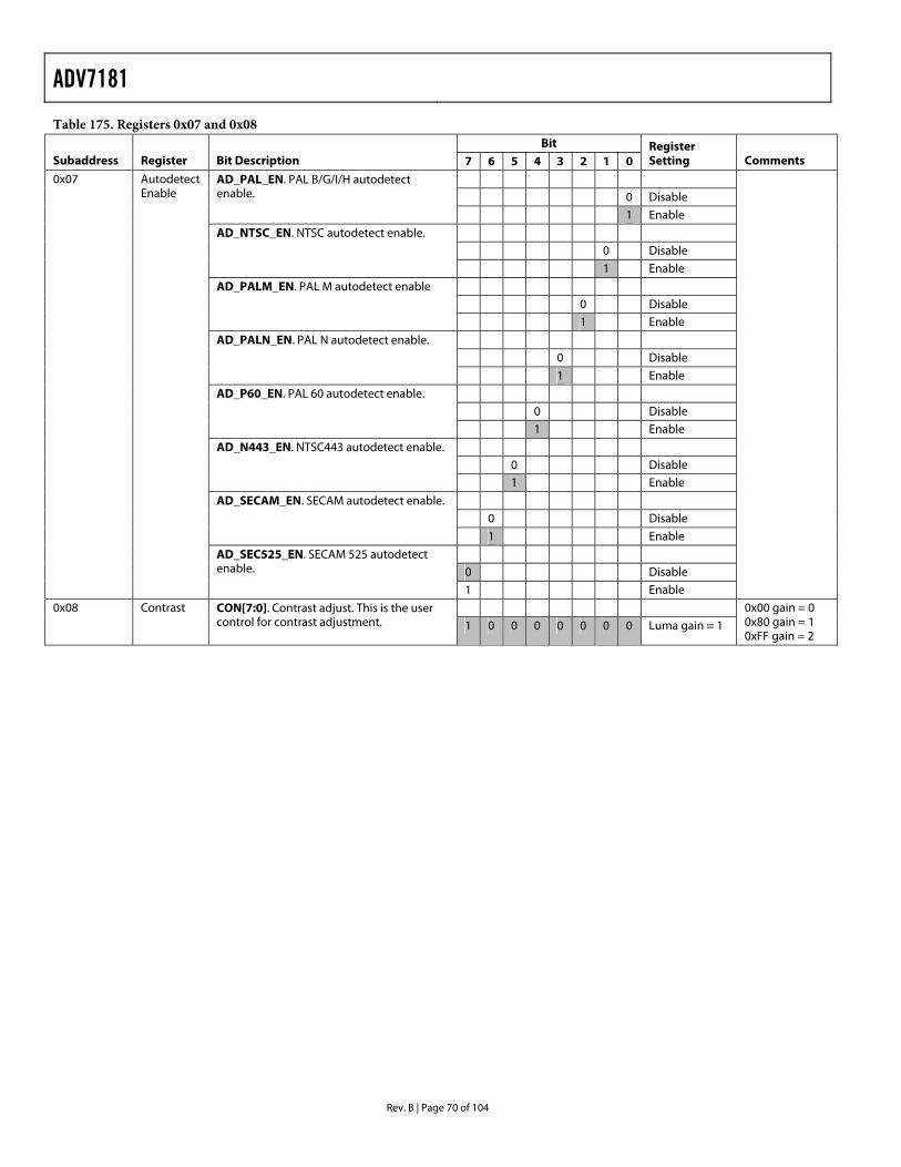
ADV7181
Rev. B | Page 70 of 104
Table 175. Registers 0x07 and 0x08 Bit
Subaddress Register Bit Description 7 6 5 4 3 2 1 0 Register Setting Comments
0 Disable AD_PAL_EN. PAL B/G/I/H autodetect enable.
1 Enable
0 Disable AD_NTSC_EN. NTSC autodetect enable.
1 Enable
0 Disable AD_PALM_EN. PAL M autodetect enable
1 Enable
0 Disable AD_PALN_EN. PAL N autodetect enable.
1 Enable
0 Disable AD_P60_EN. PAL 60 autodetect enable.
1 Enable
0 Disable AD_N443_EN. NTSC443 autodetect enable.
1 Enable
0 Disable AD_SECAM_EN. SECAM autodetect enable.
1 Enable
0 Disable
0x07 Autodetect Enable
AD_SEC525_EN. SECAM 525 autodetect enable.
1 Enable
0x08 Contrast CON[7:0]. Contrast adjust. This is the user control for contrast adjustment. 1 0 0 0 0 0 0 0 Luma gain = 1
0x00 gain = 0 0x80 gain = 1 0xFF gain = 2
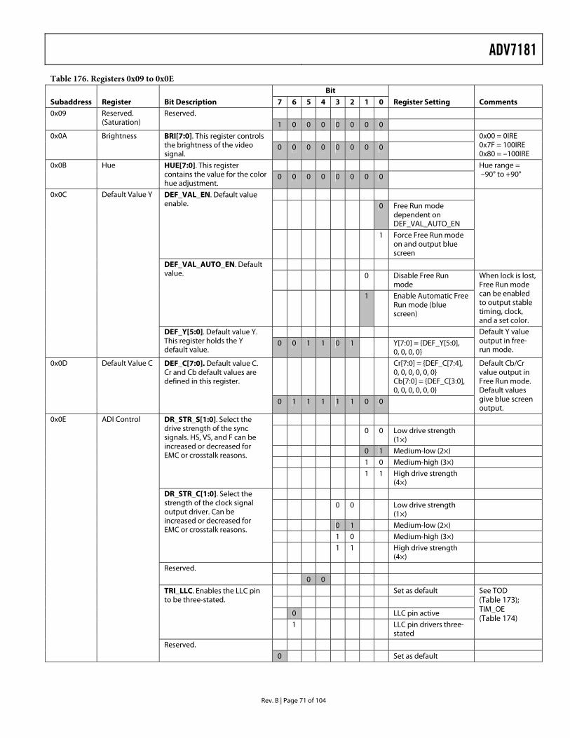
ADV7181
Rev. B | Page 71 of 104
Table 176. Registers 0x09 to 0x0E Bit
Subaddress Register Bit Description 7 6 5 4 3 2 1 0 Register Setting Comments 0x09 Reserved.
(Saturation) Reserved.
1 0 0 0 0 0 0 0
0x0A Brightness BRI[7:0]. This register controls the brightness of the video signal.
0 0 0 0 0 0 0 0
0x00 = 0IRE 0x7F = 100IRE 0x80 = –100IRE
0x0B Hue HUE[7:0]. This register contains the value for the color hue adjustment.
0 0 0 0 0 0 0 0
Hue range = –90° to +90°
0 Free Run mode dependent on DEF_VAL_AUTO_EN
DEF_VAL_EN. Default value enable.
1 Force Free Run mode on and output blue screen
0 Disable Free Run mode
DEF_VAL_AUTO_EN. Default value.
1 Enable Automatic Free Run mode (blue screen)
When lock is lost, Free Run mode can be enabled to output stable timing, clock, and a set color.
0x0C Default Value Y
DEF_Y[5:0]. Default value Y. This register holds the Y default value.
0 0 1 1 0 1 Y[7:0] = DEF_Y[5:0], 0, 0, 0, 0
Default Y value output in free-run mode.
Cr[7:0] = DEF_C[7:4], 0, 0, 0, 0, 0, 0 Cb[7:0] = DEF_C[3:0], 0, 0, 0, 0, 0, 0
0x0D Default Value C DEF_C[7:0]. Default value C. Cr and Cb default values are defined in this register.
0 1 1 1 1 1 0 0
Default Cb/Cr value output in Free Run mode. Default values give blue screen output.
0 0 Low drive strength (1×)
0 1 Medium-low (2×)
1 0 Medium-high (3×)
DR_STR_S[1:0]. Select the drive strength of the sync signals. HS, VS, and F can be increased or decreased for EMC or crosstalk reasons.
1 1 High drive strength (4×)
0 0 Low drive strength (1×)
0 1 Medium-low (2×)
1 0 Medium-high (3×)
DR_STR_C[1:0]. Select the strength of the clock signal output driver. Can be increased or decreased for EMC or crosstalk reasons.
1 1 High drive strength (4×)
Reserved.
0 0
Set as default
0 LLC pin active
TRI_LLC. Enables the LLC pin to be three-stated.
1 LLC pin drivers three-stated
See TOD (Table 173); TIM_OE (Table 174)
0x0E ADI Control
Reserved.
0 Set as default
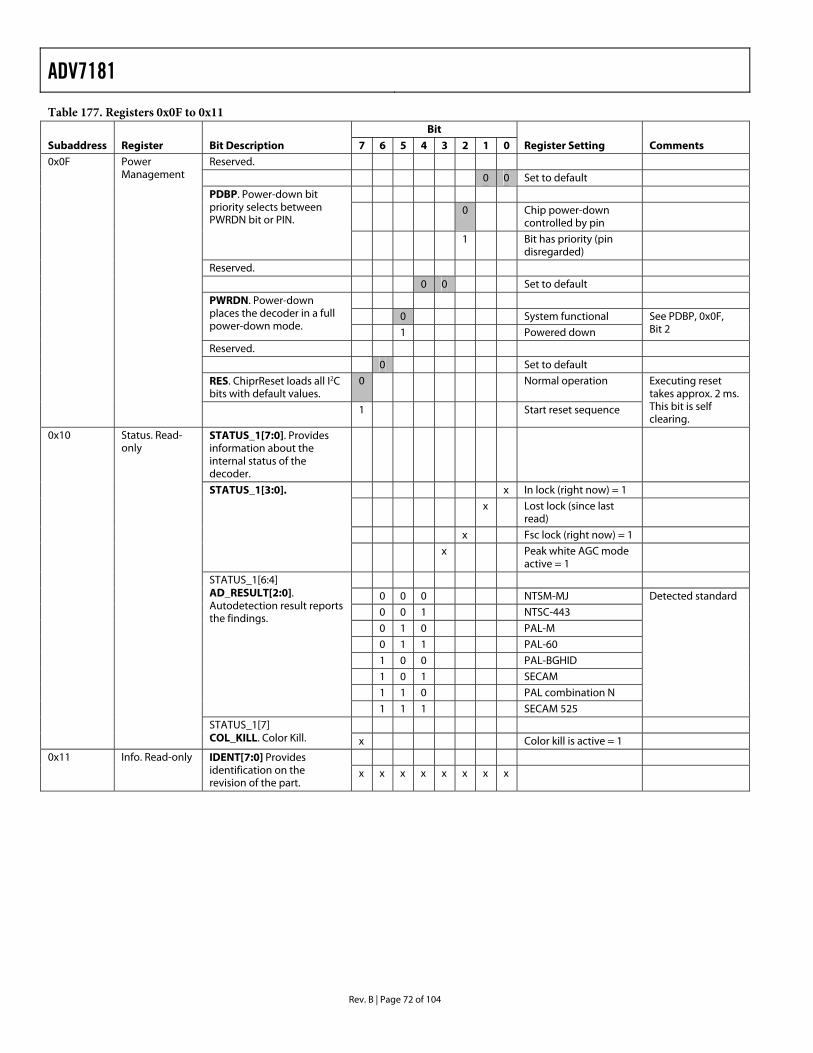
ADV7181
Rev. B | Page 72 of 104
Table 177. Registers 0x0F to 0x11 Bit
Subaddress Register Bit Description 7 6 5 4 3 2 1 0 Register Setting Comments Reserved.
0 0 Set to default
0 Chip power-down controlled by pin
PDBP. Power-down bit priority selects between PWRDN bit or PIN.
1 Bit has priority (pin disregarded)
Reserved.
0 0 Set to default
0 System functional PWRDN. Power-down places the decoder in a full power-down mode.
1 Powered down
See PDBP, 0x0F, Bit 2
Reserved.
0 Set to default
RES. ChiprReset loads all I2C bits with default values.
0 Normal operation
0x0F Power Management
1 Start reset sequence
Executing reset takes approx. 2 ms. This bit is self clearing.
STATUS_1[7:0]. Provides information about the internal status of the decoder.
x In lock (right now) = 1
x Lost lock (since last read)
x Fsc lock (right now) = 1
STATUS_1[3:0].
x Peak white AGC mode active = 1
0 0 0 NTSM-MJ
0 0 1 NTSC-443
0 1 0 PAL-M
0 1 1 PAL-60
1 0 0 PAL-BGHID
1 0 1 SECAM
1 1 0 PAL combination N
STATUS_1[6:4] AD_RESULT[2:0]. Autodetection result reports the findings.
1 1 1 SECAM 525
Detected standard
0x10 Status. Read-only
STATUS_1[7] COL_KILL. Color Kill. x Color kill is active = 1
0x11 Info. Read-only IDENT[7:0] Provides identification on the revision of the part.
x x x x x x x x
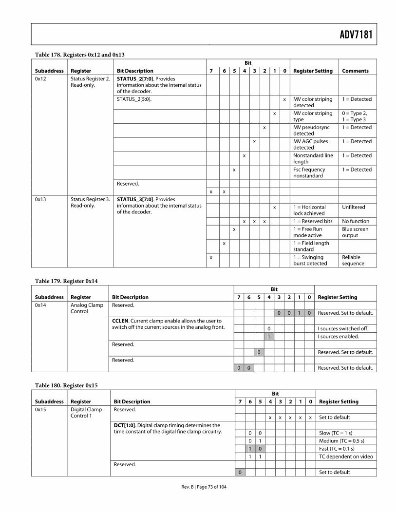
ADV7181
Rev. B | Page 73 of 104
Table 178. Registers 0x12 and 0x13 Bit
Subaddress Register Bit Description 7 6 5 4 3 2 1 0 Register Setting Comments
STATUS_2[7:0]. Provides information about the internal status of the decoder.
STATUS_2[5:0]. x MV color striping detected
1 = Detected
x MV color striping type
0 = Type 2, 1 = Type 3
x MV pseudosync detected
1 = Detected
x MV AGC pulses detected
1 = Detected
x Nonstandard line length
1 = Detected
x Fsc frequency nonstandard
1 = Detected
0x12 Status Register 2. Read-only.
Reserved.
x x
x 1 = Horizontal lock achieved
Unfiltered
x x x 1 = Reserved bits No function
x 1 = Free Run mode active
Blue screen output
x 1 = Field length standard
0x13 Status Register 3. Read-only.
STATUS_3[7:0]. Provides information about the internal status of the decoder.
x 1 = Swinging burst detected
Reliable sequence
Table 179. Register 0x14 Bit
Subaddress Register Bit Description 7 6 5 4 3 2 1 0 Register Setting Reserved.
0 0 1 0 Reserved. Set to default.
0 I sources switched off. CCLEN. Current clamp enable allows the user to switch off the current sources in the analog front.
1 I sources enabled.
Reserved.
0 Reserved. Set to default.
0x14 Analog Clamp Control
Reserved.
0 0 Reserved. Set to default.
Table 180. Register 0x15 Bit
Subaddress Register Bit Description 7 6 5 4 3 2 1 0 Register Setting Reserved.
x x x x x Set to default
0 0 Slow (TC = 1 s)
0 1 Medium (TC = 0.5 s)
1 0 Fast (TC = 0.1 s)
DCT[1:0]. Digital clamp timing determines the time constant of the digital fine clamp circuitry.
1 1 TC dependent on video
Reserved.
0x15 Digital Clamp Control 1
0 Set to default
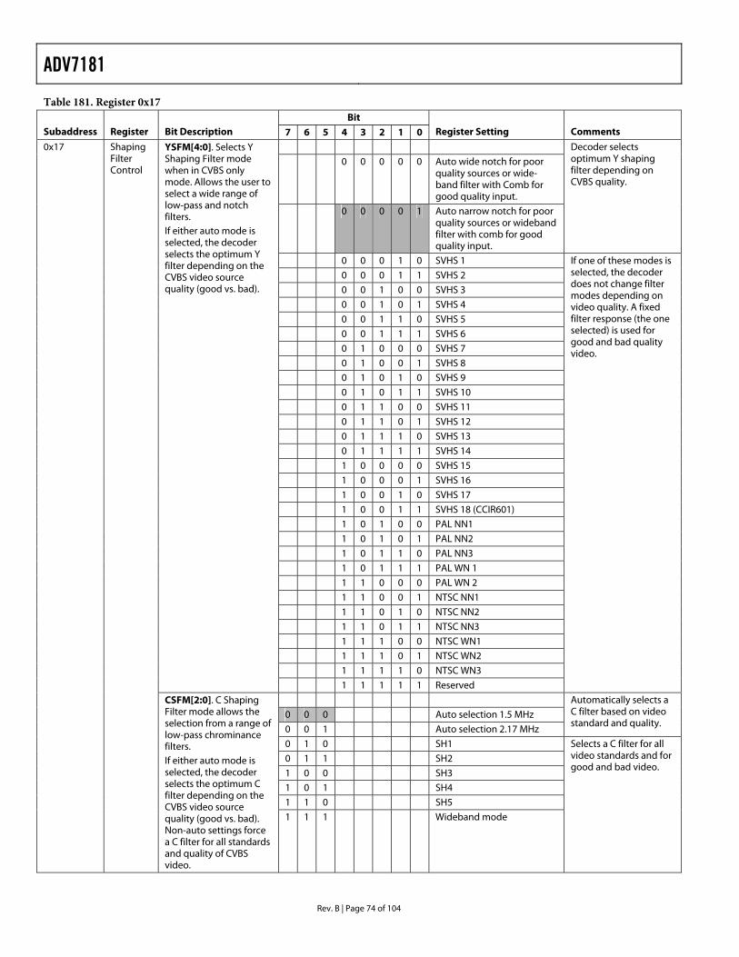
ADV7181
Rev. B | Page 74 of 104
Table 181. Register 0x17 Bit
Subaddress Register Bit Description 7 6 5 4 3 2 1 0 Register Setting Comments
0 0 0 0 0 Auto wide notch for poor quality sources or wide-band filter with Comb for good quality input.
0 0 0 0 1 Auto narrow notch for poor quality sources or wideband filter with comb for good quality input.
Decoder selects optimum Y shaping filter depending on CVBS quality.
0 0 0 1 0 SVHS 1
0 0 0 1 1 SVHS 2
0 0 1 0 0 SVHS 3
0 0 1 0 1 SVHS 4
0 0 1 1 0 SVHS 5
0 0 1 1 1 SVHS 6
0 1 0 0 0 SVHS 7
0 1 0 0 1 SVHS 8
0 1 0 1 0 SVHS 9
0 1 0 1 1 SVHS 10
0 1 1 0 0 SVHS 11
0 1 1 0 1 SVHS 12
0 1 1 1 0 SVHS 13
0 1 1 1 1 SVHS 14
1 0 0 0 0 SVHS 15
1 0 0 0 1 SVHS 16
1 0 0 1 0 SVHS 17
1 0 0 1 1 SVHS 18 (CCIR601)
1 0 1 0 0 PAL NN1
1 0 1 0 1 PAL NN2
1 0 1 1 0 PAL NN3
1 0 1 1 1 PAL WN 1
1 1 0 0 0 PAL WN 2
1 1 0 0 1 NTSC NN1
1 1 0 1 0 NTSC NN2
1 1 0 1 1 NTSC NN3
1 1 1 0 0 NTSC WN1
1 1 1 0 1 NTSC WN2
1 1 1 1 0 NTSC WN3
YSFM[4:0]. Selects Y Shaping Filter mode when in CVBS only mode. Allows the user to select a wide range of low-pass and notch filters. If either auto mode is selected, the decoder selects the optimum Y filter depending on the CVBS video source quality (good vs. bad).
1 1 1 1 1 Reserved
If one of these modes is selected, the decoder does not change filter modes depending on video quality. A fixed filter response (the one selected) is used for good and bad quality video.
0 0 0 Auto selection 1.5 MHz
0 0 1 Auto selection 2.17 MHz
Automatically selects a C filter based on video standard and quality.
0 1 0 SH1
0 1 1 SH2
1 0 0 SH3
1 0 1 SH4
1 1 0 SH5
0x17 Shaping Filter Control
CSFM[2:0]. C Shaping Filter mode allows the selection from a range of low-pass chrominance filters. If either auto mode is selected, the decoder selects the optimum C filter depending on the CVBS video source quality (good vs. bad). Non-auto settings force a C filter for all standards and quality of CVBS video.
1 1 1 Wideband mode
Selects a C filter for all video standards and for good and bad video.
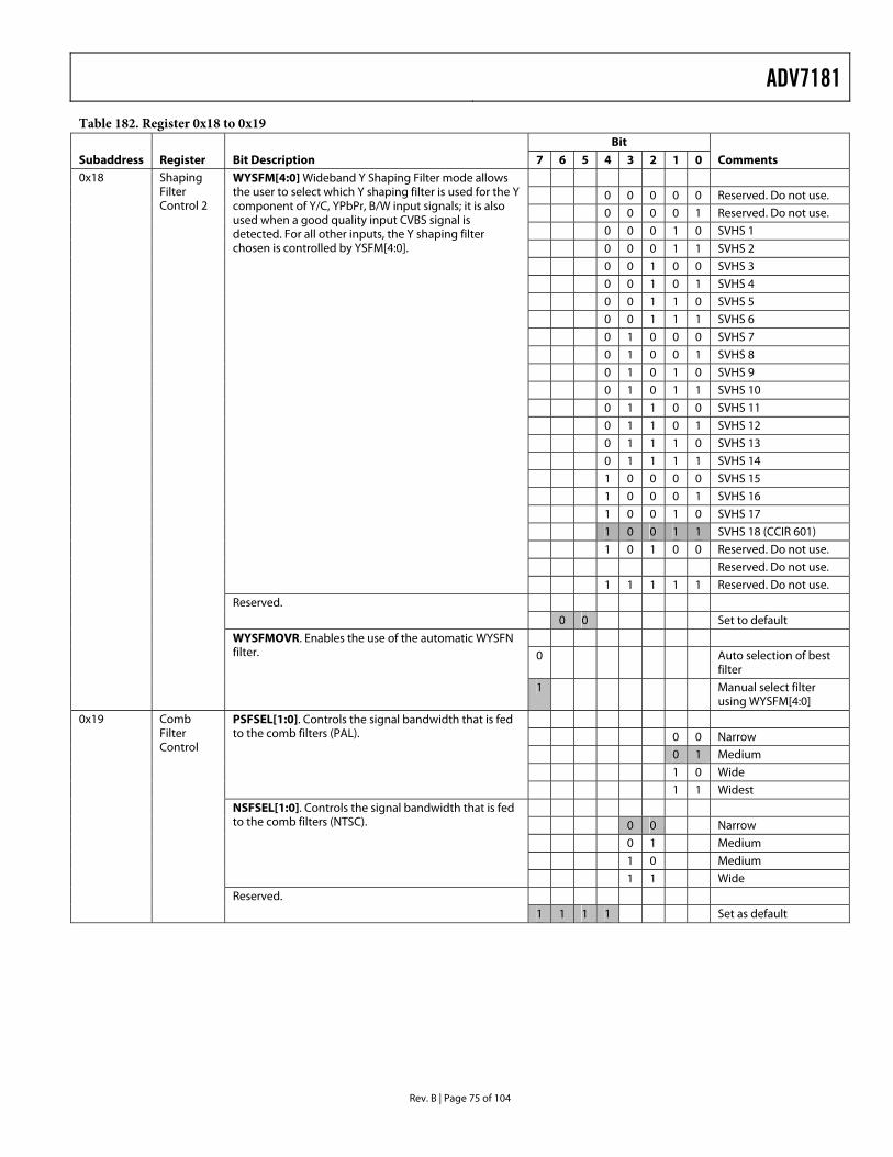
ADV7181
Rev. B | Page 75 of 104
Table 182. Register 0x18 to 0x19 Bit
Subaddress Register Bit Description 7 6 5 4 3 2 1 0 Comments
0 0 0 0 0 Reserved. Do not use.
0 0 0 0 1 Reserved. Do not use.
0 0 0 1 0 SVHS 1
0 0 0 1 1 SVHS 2
0 0 1 0 0 SVHS 3
0 0 1 0 1 SVHS 4
0 0 1 1 0 SVHS 5
0 0 1 1 1 SVHS 6
0 1 0 0 0 SVHS 7
0 1 0 0 1 SVHS 8
0 1 0 1 0 SVHS 9
0 1 0 1 1 SVHS 10
0 1 1 0 0 SVHS 11
0 1 1 0 1 SVHS 12
0 1 1 1 0 SVHS 13
0 1 1 1 1 SVHS 14
1 0 0 0 0 SVHS 15
1 0 0 0 1 SVHS 16
1 0 0 1 0 SVHS 17
1 0 0 1 1 SVHS 18 (CCIR 601)
1 0 1 0 0 Reserved. Do not use.
Reserved. Do not use.
WYSFM[4:0] Wideband Y Shaping Filter mode allows the user to select which Y shaping filter is used for the Y component of Y/C, YPbPr, B/W input signals; it is also used when a good quality input CVBS signal is detected. For all other inputs, the Y shaping filter chosen is controlled by YSFM[4:0].
1 1 1 1 1 Reserved. Do not use.
Reserved.
0 0 Set to default
0 Auto selection of best filter
0x18 Shaping Filter Control 2
WYSFMOVR. Enables the use of the automatic WYSFN filter.
1 Manual select filter using WYSFM[4:0]
0 0 Narrow
0 1 Medium
1 0 Wide
PSFSEL[1:0]. Controls the signal bandwidth that is fed to the comb filters (PAL).
1 1 Widest
0 0 Narrow
0 1 Medium
1 0 Medium
NSFSEL[1:0]. Controls the signal bandwidth that is fed to the comb filters (NTSC).
1 1 Wide
0x19 Comb Filter Control
Reserved.
1 1 1 1 Set as default
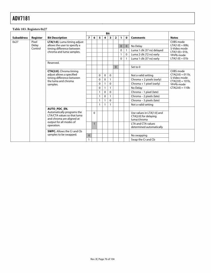
ADV7181
Rev. B | Page 76 of 104
Table 183. Registers 0x27 Bit
Subaddress Register Bit Description 7 6 5 4 3 2 1 0 Comments Notes
0 0 No Delay
0 1 Luma 1 clk (37 ns) delayed
1 0 Luma 2 clk (72 ns) early
LTA[1:0]. Luma timing adjust allows the user to specify a timing difference between chroma and luma samples.
0 1 Luma 1 clk (37 ns) early
CVBS mode LTA[1:0] = 00b; S-Video mode LTA[1:0]= 01b, YPrPb mode LTA[1:0] = 01b
Reserved.
0 Set to 0
0 0 0 Not a valid setting
0 0 1 Chroma + 2 pixels (early)
0 1 0 Chroma + 1 pixel (early)
0 1 1 No Delay
1 0 0 Chroma – 1 pixel (late)
1 0 1 Chroma – 2 pixels (late)
1 1 0 Chroma – 3 pixels (late)
CTA[2:0]. Chroma timing adjust allows a specified timing difference between the luma and chroma samples.
1 1 1 Not a valid setting
CVBS mode CTA[2:0] = 011b, S-Video mode CTA[2:0] = 101b, YPrPb mode CTA[2:0] = 110b
0 Use values in LTA[1:0] and CTA[2:0] for delaying luma/chroma
AUTO_PDC_EN. Automatically programs the LTA/CTA values so that luma and chroma are aligned at output for all modes of operation. 1 LTA and CTA values
determined automatically
0 No swapping
0x27 Pixel Delay Control
SWPC. Allows the Cr and Cb samples to be swapped.
1 Swap the Cr and Cb
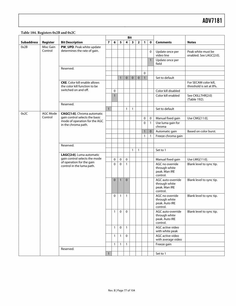
ADV7181
Rev. B | Page 77 of 104
Table 184. Registers 0x2B and 0x2C Bit
Subaddress Register Bit Description 7 6 5 4 3 2 1 0 Comments Notes
0 Update once per video line
PW_UPD. Peak white update determines the rate of gain.
1 Update once per field
Peak white must be enabled. See LAGC[2:0].
0
Reserved.
1 0 0 0 1 Set to default
For SECAM color kill, threshold is set at 8%.
0 Color kill disabled
CKE. Color kill enable allows the color kill function to be switched on and off.
1 Color kill enabled See CKILLTHR[2:0] (Table 192).
0x2B Misc Gain Control
Reserved.
1 1 1 Set to default
0 0 Manual fixed gain Use CMG[11:0].
0 1 Use luma gain for chroma
1 0 Automatic gain Based on color burst.
1 1 Freeze chroma gain
CAGC[1:0]. Chroma automatic gain control selects the basic mode of operation for the AGC in the chroma path.
Reserved.
1 1 Set to 1
0 0 0 Manual fixed gain Use LMG[11:0].
0 0 1 AGC no override through white peak. Man IRE control.
Blank level to sync tip.
0 1 0 AGC auto-override through white peak. Man IRE control.
Blank level to sync tip.
0 1 1 AGC no override through white peak. Auto IRE control.
Blank level to sync tip.
1 0 0 AGC auto-override through white peak. Auto IRE control.
Blank level to sync tip.
1 0 1 AGC active video with white peak
1 1 0 AGC active video with average video
LAGC[2:0]. Luma automatic gain control selects the mode of operation for the gain control in the luma path.
1 1 1 Freeze gain
0x2C AGC Mode Control
Reserved.
1 Set to 1
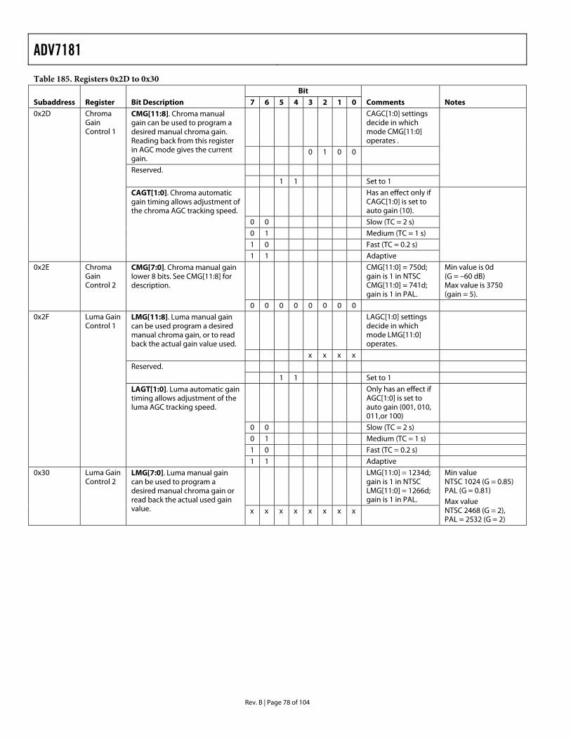
ADV7181
Rev. B | Page 78 of 104
Table 185. Registers 0x2D to 0x30 Bit
Subaddress Register Bit Description 7 6 5 4 3 2 1 0 Comments Notes CAGC[1:0] settings
decide in which mode CMG[11:0] operates .
CMG[11:8]. Chroma manual gain can be used to program a desired manual chroma gain. Reading back from this register in AGC mode gives the current gain.
0 1 0 0
Reserved.
1 1 Set to 1
Has an effect only if CAGC[1:0] is set to auto gain (10).
0 0 Slow (TC = 2 s)
0 1 Medium (TC = 1 s)
1 0 Fast (TC = 0.2 s)
0x2D Chroma Gain Control 1
CAGT[1:0]. Chroma automatic gain timing allows adjustment of the chroma AGC tracking speed.
1 1 Adaptive
CMG[11:0] = 750d; gain is 1 in NTSC CMG[11:0] = 741d; gain is 1 in PAL.
Min value is 0d (G = –60 dB) Max value is 3750 (gain = 5).
0x2E Chroma Gain Control 2
CMG[7:0]. Chroma manual gain lower 8 bits. See CMG[11:8] for description.
0 0 0 0 0 0 0 0
LAGC[1:0] settings decide in which mode LMG[11:0] operates.
LMG[11:8]. Luma manual gain can be used program a desired manual chroma gain, or to read back the actual gain value used.
x x x x
Reserved.
1 1 Set to 1
Only has an effect if AGC[1:0] is set to auto gain (001, 010, 011,or 100)
0 0 Slow (TC = 2 s)
0 1 Medium (TC = 1 s)
1 0 Fast (TC = 0.2 s)
0x2F Luma Gain Control 1
LAGT[1:0]. Luma automatic gain timing allows adjustment of the luma AGC tracking speed.
1 1 Adaptive
LMG[11:0] = 1234d; gain is 1 in NTSC LMG[11:0] = 1266d; gain is 1 in PAL.
0x30 Luma Gain Control 2
LMG[7:0]. Luma manual gain can be used to program a desired manual chroma gain or read back the actual used gain value. x x x x x x x x
Min value NTSC 1024 (G = 0.85) PAL (G = 0.81) Max value NTSC 2468 (G = 2), PAL = 2532 (G = 2)
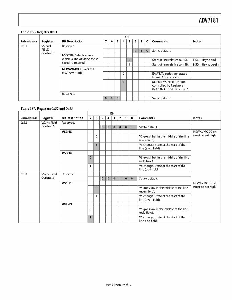
ADV7181
Rev. B | Page 79 of 104
Table 186. Register 0x31 Bit
Subaddress Register Bit Description 7 6 5 4 3 2 1 0 Comments Notes Reserved.
0 1 0 Set to default.
0 Start of line relative to HSE. HSE = Hsync end HVSTIM. Selects where within a line of video the VS signal is asserted.
1 Start of line relative to HSB. HSB = Hsync begin
0 EAV/SAV codes generated to suit ADI encoders.
NEWAVMODE. Sets the EAV/SAV mode.
1 Manual VS/Field position controlled by Registers 0x32, 0x33, and 0xE5–0xEA.
0x31 VS and FIELD Control 1
Reserved.
0 0 0 Set to default.
Table 187. Registers 0x32 and 0x33 Bit
Subaddress Register
Bit Description 7 6 5 4 3 2 1 0 Comments Notes
Reserved.
0 0 0 0 0 1 Set to default.
VSBHE
0 VS goes high in the middle of the line (even field).
1 VS changes state at the start of the line (even field).
VSBHO
0 VS goes high in the middle of the line (odd field).
0x32 VSync Field Control 2
1 VS changes state at the start of the line (odd field).
Reserved.
0 0 0 1 0 0 Set to default.
NEWAVMODE bit must be set high.
VSEHE
0 VS goes low in the middle of the line (even field).
1 VS changes state at the start of the line (even field).
VSEHO
0 VS goes low in the middle of the line (odd field).
0x33 VSync Field Control 3
1 VS changes state at the start of the line odd field.
NEWAVMODE bit must be set high.
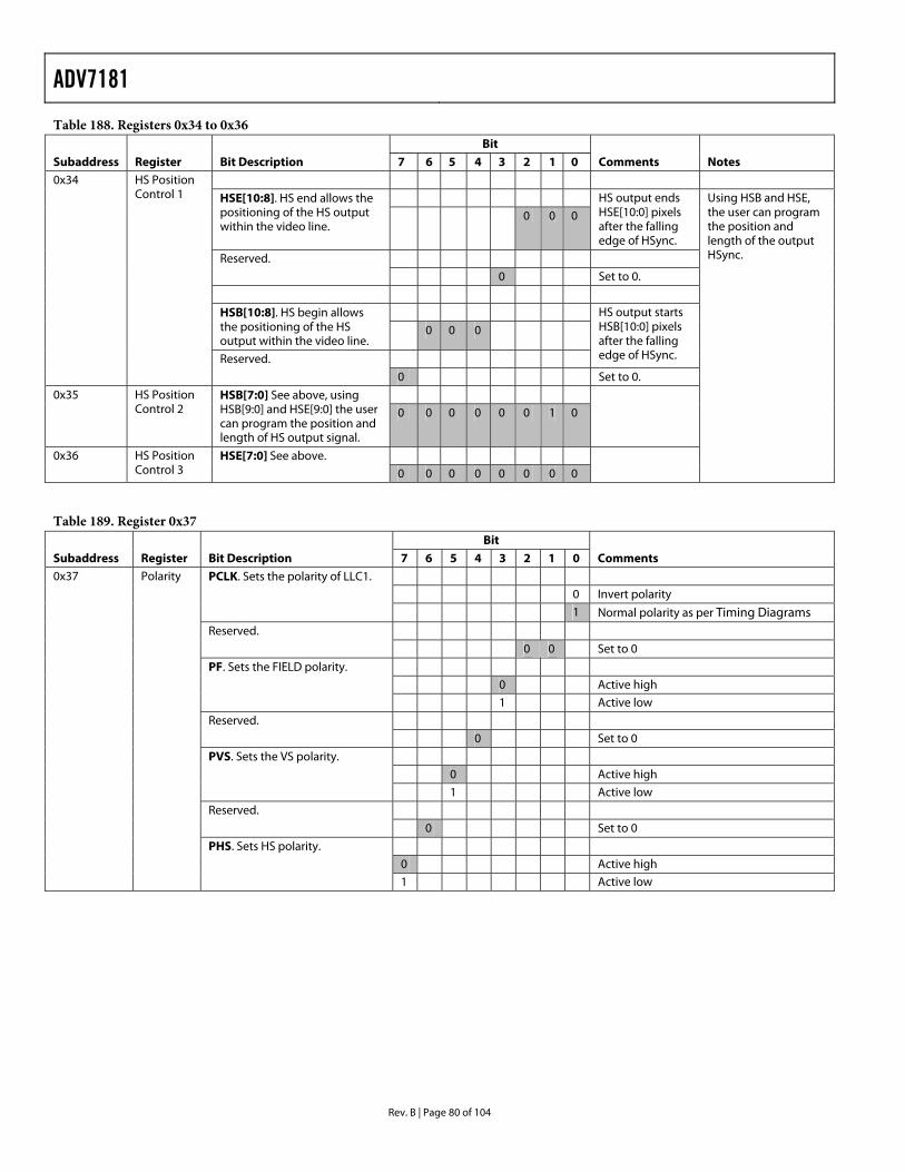
ADV7181
Rev. B | Page 80 of 104
Table 188. Registers 0x34 to 0x36 Bit
Subaddress Register Bit Description 7 6 5 4 3 2 1 0 Comments Notes
HSE[10:8]. HS end allows the positioning of the HS output within the video line.
0 0 0
HS output ends HSE[10:0] pixels after the falling edge of HSync.
Reserved.
0 Set to 0.
HSB[10:8]. HS begin allows the positioning of the HS output within the video line.
0 0 0
HS output starts HSB[10:0] pixels after the falling edge of HSync.
0x34 HS Position Control 1
Reserved.
0 Set to 0.
0x35 HS Position Control 2
HSB[7:0] See above, using HSB[9:0] and HSE[9:0] the user can program the position and length of HS output signal.
0 0 0 0 0 0 1 0
0x36 HS Position Control 3
HSE[7:0] See above. 0 0 0 0 0 0 0 0
Using HSB and HSE, the user can program the position and length of the output HSync.
Table 189. Register 0x37 Bit
Subaddress Register Bit Description 7 6 5 4 3 2 1 0 Comments
0 Invert polarity PCLK. Sets the polarity of LLC1.
1 Normal polarity as per Timing Diagrams
Reserved.
0 0 Set to 0
0 Active high PF. Sets the FIELD polarity.
1 Active low
Reserved.
0 Set to 0
0 Active high PVS. Sets the VS polarity.
1 Active low
Reserved.
0 Set to 0
0 Active high
0x37 Polarity
PHS. Sets HS polarity.
1 Active low
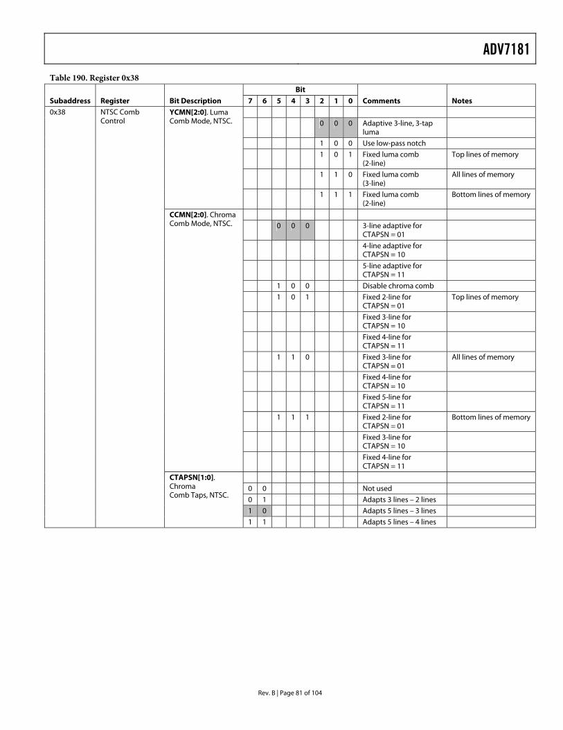
ADV7181
Rev. B | Page 81 of 104
Table 190. Register 0x38 Bit
Subaddress Register Bit Description 7 6 5 4 3 2 1 0 Comments Notes
0 0 0 Adaptive 3-line, 3-tap luma
1 0 0 Use low-pass notch
1 0 1 Fixed luma comb (2-line)
Top lines of memory
1 1 0 Fixed luma comb (3-line)
All lines of memory
YCMN[2:0]. Luma Comb Mode, NTSC.
1 1 1 Fixed luma comb (2-line)
Bottom lines of memory
0 0 0 3-line adaptive for CTAPSN = 01
4-line adaptive for CTAPSN = 10
5-line adaptive for CTAPSN = 11
1 0 0 Disable chroma comb
1 0 1 Fixed 2-line for CTAPSN = 01
Top lines of memory
Fixed 3-line for CTAPSN = 10
Fixed 4-line for CTAPSN = 11
1 1 0 Fixed 3-line for CTAPSN = 01
All lines of memory
Fixed 4-line for CTAPSN = 10
Fixed 5-line for CTAPSN = 11
1 1 1 Fixed 2-line for CTAPSN = 01
Bottom lines of memory
Fixed 3-line for CTAPSN = 10
CCMN[2:0]. Chroma Comb Mode, NTSC.
Fixed 4-line for CTAPSN = 11
0 0 Not used
0 1 Adapts 3 lines – 2 lines
1 0 Adapts 5 lines – 3 lines
0x38 NTSC Comb Control
CTAPSN[1:0]. Chroma Comb Taps, NTSC.
1 1 Adapts 5 lines – 4 lines
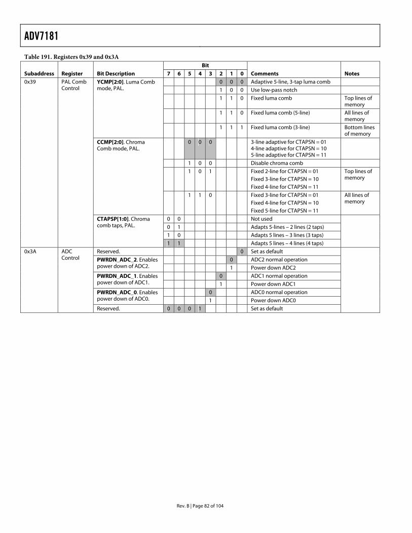
ADV7181
Rev. B | Page 82 of 104
Table 191. Registers 0x39 and 0x3A Bit
Subaddress Register Bit Description 7 6 5 4 3 2 1 0 Comments Notes 0 0 0 Adaptive 5-line, 3-tap luma comb
1 0 0 Use low-pass notch
1 1 0 Fixed luma comb Top lines of memory
1 1 0 Fixed luma comb (5-line) All lines of memory
YCMP[2:0]. Luma Comb mode, PAL.
1 1 1 Fixed luma comb (3-line) Bottom lines of memory
0 0 0 3-line adaptive for CTAPSN = 01 4-line adaptive for CTAPSN = 10 5-line adaptive for CTAPSN = 11
1 0 0 Disable chroma comb
1 0 1 Fixed 2-line for CTAPSN = 01 Fixed 3-line for CTAPSN = 10 Fixed 4-line for CTAPSN = 11
Top lines of memory
CCMP[2:0]. Chroma Comb mode, PAL.
1 1 0 Fixed 3-line for CTAPSN = 01 Fixed 4-line for CTAPSN = 10 Fixed 5-line for CTAPSN = 11
All lines of memory
0 0 Not used
0 1 Adapts 5-lines – 2 lines (2 taps)
1 0 Adapts 5 lines – 3 lines (3 taps)
0x39 PAL Comb Control
CTAPSP[1:0]. Chroma comb taps, PAL.
1 1 Adapts 5 lines – 4 lines (4 taps)
Reserved. 0 Set as default
0 ADC2 normal operation PWRDN_ADC_2. Enables power down of ADC2. 1 Power down ADC2
0 ADC1 normal operation PWRDN_ADC_1. Enables power down of ADC1. 1 Power down ADC1
0 ADC0 normal operation PWRDN_ADC_0. Enables power down of ADC0. 1 Power down ADC0
0x3A ADC Control
Reserved. 0 0 0 1 Set as default
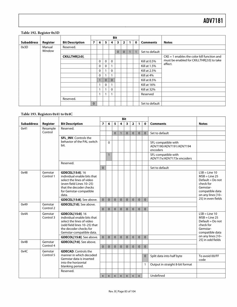
ADV7181
Rev. B | Page 83 of 104
Table 192. Register 0x3D Bit
Subaddress Register Bit Description 7 6 5 4 3 2 1 0 Comments Notes Reserved.
0 0 1 1 Set to default
CKILLTHR[2:0].
0 0 0 Kill at 0.5%
0 0 1 Kill at 1.5%
0 1 0 Kill at 2.5%
0 1 1 Kill at 4%
1 0 0 Kill at 8.5%
CKE = 1 enables the color kill function and must be enabled for CKILLTHR[2:0] to take effect.
1 0 1 Kill at 16%
1 1 0 Kill at 32%
1 1 1 Reserved
Reserved.
0x3D Manual Window
0 Set to default
Table 193. Registers 0x41 to 0x4C Bit
Subaddress Register Bit Description 7 6 5 4 3 2 1 0 Comments Notes Reserved.
0 1 0 0 0 0 Set to default
0 SFL-compatible with ADV7190/ADV7191/ADV7194 encoders
SFL_INV. Controls the behavior of the PAL switch bit.
1 SFL-compatible with ADV717x/ADV7173x encoders
0x41 Resample Control
Reserved.
0 Set to default
GDECEL[15:0]. 16 individual enable bits that select the lines of video (even field Lines 10–25) that the decoder checks for Gemstar-compatible data.
0x48 Gemstar Control 1
GDECEL[15:8]. See above. 0 0 0 0 0 0 0 0
0x49 Gemstar Control 2
GDECEL[7:0]. See above. 0 0 0 0 0 0 0 0
LSB = Line 10 MSB = Line 25 Default = Do not check for Gemstar-compatible data on any lines [10–25] in even fields
GDECOL[15:0]. 16 individual enable bits that select the lines of video (odd field lines 10–25) that the decoder checks for Gemstar-compatible data.
0x4A Gemstar Control 3
GDECOL[15:8]. See above. 0 0 0 0 0 0 0 0
0x4B Gemstar Control 4
GDECOL[7:0]. See above. 0 0 0 0 0 0 0 0
LSB = Line 10 MSB = Line 25 Default = Do not check for Gemstar-compatible data on any lines [10–25] in odd fields
0 Split data into half byte To avoid 00/FF code
GDECAD. Controls the manner in which decoded Gemstar data is inserted into the horizontal blanking period. 1 Output in straight 8-bit format
0x4C Gemstar Control 5
Reserved.
x x x x x x x Undefined
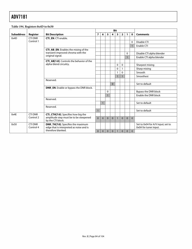
ADV7181
Rev. B | Page 84 of 104
Table 194. Registers 0x4D to 0x50 Bit
Subaddress Register Bit Description 7 6 5 4 3 2 1 0 Comments
0 Disable CTI CTI_EN. CTI enable.
1 Enable CTI
0 Disable CTI alpha blender CTI_AB_EN. Enables the mixing of the transient improved chroma with the original signal.
1 Enable CTI alpha blender
0 0 Sharpest mixing
0 1 Sharp mixing
1 0 Smooth
CTI_AB[1:0]. Controls the behavior of the alpha-blend circuitry.
1 1 Smoothest
Reserved.
0 Set to default
0 Bypass the DNR block DNR_EN. Enable or bypass the DNR block.
1 Enable the DNR block
Reserved.
1 Set to default
0x4D CTI DNR Control 1
Reserved.
1 Set to default
0x4E CTI DNR Control 2
CTI_CTH[7:0]. Specifies how big the amplitude step must be to be steepened by the CTI block.
0 0 0 0 1 0 0 0
Set to 0x04 for A/V input; set to 0x0A for tuner input.
0x50 CTI DNR Control 4
DNR_TH[7:0]. Specifies the maximum edge that is interpreted as noise and is therefore blanked. 0 0 0 0 1 0 0 0
ADV7181
Rev. B | Page 85 of 104
Table 195. Register 0x51 Bit
Subaddress Register Bit Description 7 6 5 4 3 2 1 0 Comments Notes
0 0 0 1 line of video
0 0 1 2 lines of video
0 1 0 5 lines of video
0 1 1 10 lines of video
1 0 0 100 lines of video
1 0 1 500 lines of video
1 1 0 1000 lines of video
CIL[2:0]. Count-into-lock determines the number of lines the system must remain in lock before showing a locked status.
1 1 1 100000 lines of video
0 0 0 1 line of video
0 0 1 2 lines of video
0 1 0 5 lines of video
0 1 1 10 lines of video
1 0 0 100 lines of video
1 0 1 500 lines of video
1 1 0 1000 lines of video
COL[2:0]. Count-out-of-lock determines the number of lines the system must remain out-of-lock before showing a lost-locked status.
1 1 1 100000 lines of video
0 Over field with vertical info
SRLS. Select raw lock signal. Selects the determination of the lock status.
1 Line-to-line evaluation
FSCLE must be set to 0 in YPrPb mode if a reliable LOST_LOCK bit is set to 0.
0 Lock status set only by horizontal lock
0x51 Lock Count
FSCLE. Fsc lock enable.
1 Lock status set by horizontal lock and subcarrier lock
ADV7181
Rev. B | Page 86 of 104
Table 196. Registers 0x8F and 0x90 Bit
Subaddress Register Bit Description 7 6 5 4 3 2 1 0 Comments Notes Reserved.
0 0 0 0 Set to default
0 0 0 LLC1 (nominally 27 MHz) selected out on LLC1 pin
LLC_PAD_SEL [2:0]. Enables manual selection of clock for LLC1 pin.
1 0 1 LLC2 (nominally 13.5 MHz) selected out on LLC1 pin
For 16-bit 4:2:2 out, OF_SEL[3:0] = 0010
0x8F Free Run Line Length 1
Reserved.
0 Set to default
0 No WSS detected WSSD. Screen signaling detected.
1 WSS detected
0 No CCAP signals detected
CCAPD. Closed caption data.
1 CCAP sequence detected
0 No EDTV sequence detected
EDTVD. EDTV sequence.
1 EDTV sequence detected
0 No CGMS transition detected
CGMSD. CGMS sequence.
1 CGMS sequence decoded
0x90 VBI Info Read Mode Details
Reserved.
x x x x
Ready-only status bits
ADV7181
Rev. B | Page 87 of 104
Table 197. Registers 0x91 to 0x9D Bit
Subaddress Register Bit Description 7 6 5 4 3 2 1 0 Comments Notes 0x91 WSS1[7:0]. Wide
screen signaling data. Read-only.
WSS1[7:0]
x x x x x x x x
WSS2[7:6] are undetermined.
0x92 WSS1[7:0]. Wide screen signaling data. Read-only.
WSS2[7:0]
x x x x x x x x
0x93 EDTV1[7:0]. EDTV data. Read-only.
EDTV1[7:0]
x x x x x x x x
0x94 EDTV2[7:0]. EDTV data. Read-only.
EDTV2[7:0]
x x x x x x x x
EDTV3[7:6] are undetermined.
0x95 EDTV3[7:0]. EDTV data. Read-only.
EDTV3[7:0]
x x x x x x x x
EDTV3[5] is reserved for future use.
0x96 CGMS1[7:0]. CGMS data. Read-only.
CGMS1[7:0]
x x x x x x x x
0x97 CGMS2[7:0]. CGMS data. Read-only.
CGMS2[7:0]
x x x x x x x x
CGMS3[7:4] are undetermined.
0x98 CGMS3[7:0]. CGMS data. Read-only.
CGMS3[7:0]
x x x x x x x x
CCAP1[7] contains parity bit for Byte 0.
0x99 CCAP1[7:0]. Closed caption data. Read-only.
CCAP1[7:0]
x x x x x x x x
CCAP2[7] contains parity bit for Byte 0.
0x9A CCAP2[7:0]. Closed caption data. Read-only.
CCAP2[7:0]
x x x x x x x x
0x9B Letterbox 1. Read-only.
LB_LCT[7:0]
x x x x x x x x
Reports the number of black lines detected at top of active video.
0x9C Letterbox 2. Read-only.
LB_LCM[7:0]
x x x x x x x x
Reports the number of black lines detected in the bottom half of active video if subtitles are detected.
0x9D Letterbox 3. Read-only.
LB_LCB[7:0]
x x x x x x x x
Reports the number of black lines detected at the bottom of active video.
This feature examines the active video at the start and at the end of each field. It enables format detection even if the video is not accompanied by a CGMS or WSS sequence.
Table 198. Register 0xB2 Bit
Subaddress Register Bit Description 7 6 5 4 3 2 1 0 Comments Reserved.
0 0 Set as default.
0 Turn off CRC check. CRC_ENABLE. Enables CRC checksum decoded from CGMS packet to validate CGMSD.
1 CGMSD goes high with valid checksum.
0xB2 CRC Enable Write
Reserved.
0 0 0 1 1 Set as default.
ADV7181
Rev. B | Page 88 of 104
Table 199. Register 0xC3 Bit
Subaddress Register Bit Description 7 6 5 4 3 2 1 0 Comment (default) Note
SETADC_sw_man_en = 1
0 0 0 0 NC
0 0 0 1 AIN2
0 0 1 0 NC
0 0 1 1 NC
0 1 0 0 AIN4
0 1 0 1 AIN6
0 1 1 0 NC
0 1 1 1 NC
1 0 0 0 NC
1 0 0 1 AIN1
1 0 1 0 NC
1 0 1 1 NC
1 1 0 0 AIN3
1 1 0 1 AIN5
1 1 1 0 NC
ADC0_SW[3:0]. Manual muxing control for ADC0.
1 1 1 1 NC
0 0 0 0 NC
0 0 0 1 NC
0 0 1 0 NC
0 0 1 1 NC
0 1 0 0 AIN4
0 1 0 1 AIN6
0 1 1 0 NC
0 1 1 1 NC
1 0 0 0 NC
1 0 0 1 NC
1 0 1 0 NC
1 0 1 1 NC
1 1 0 0 AIN3
1 1 0 1 AIN5
1 1 1 0 NC
0xC3 ADC SWITCH 1
ADC1_SW[3:0]. Manual muxing control for ADC1.
1 1 1 1 NC NC = no connection.
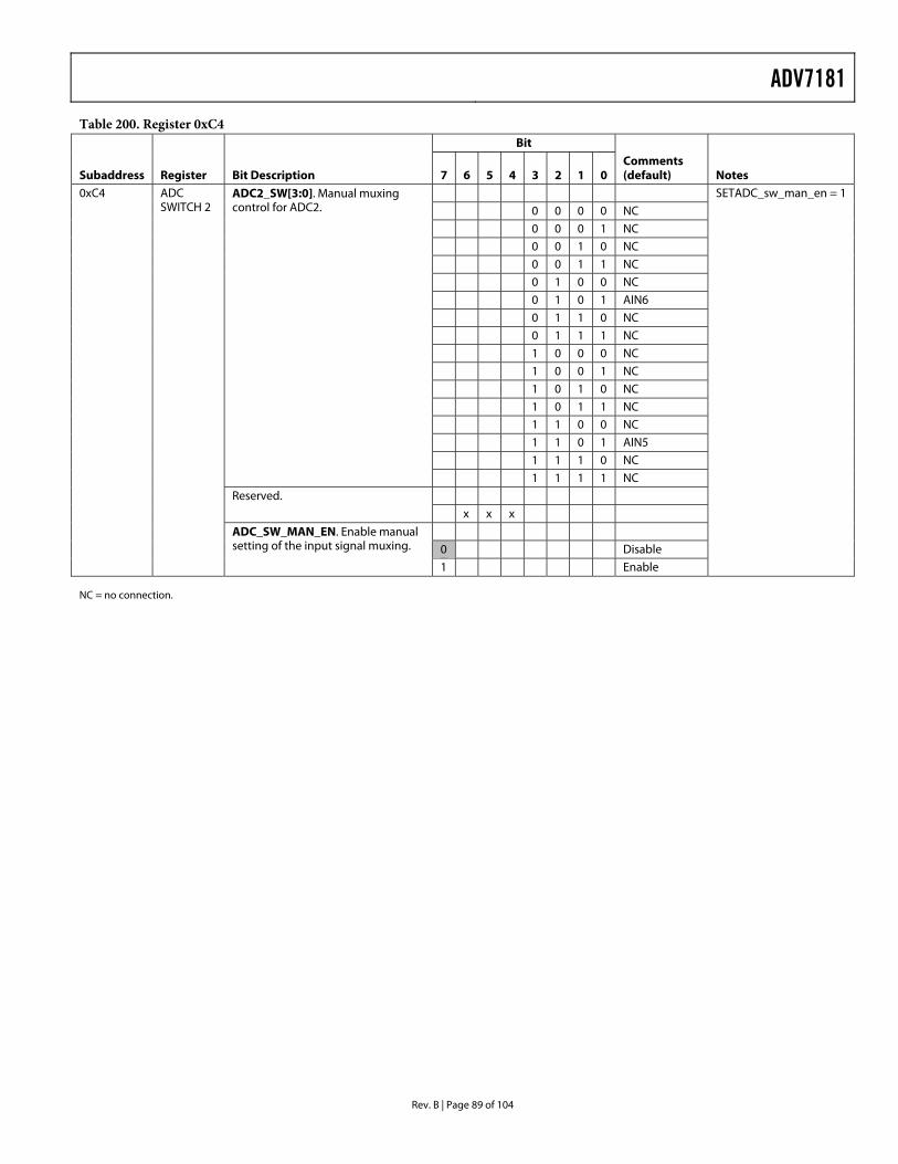
ADV7181
Rev. B | Page 89 of 104
Table 200. Register 0xC4 Bit
Subaddress Register Bit Description 7 6 5 4 3 2 1 0 Comments (default) Notes
0 0 0 0 NC
0 0 0 1 NC
0 0 1 0 NC
0 0 1 1 NC
0 1 0 0 NC
0 1 0 1 AIN6
0 1 1 0 NC
0 1 1 1 NC
1 0 0 0 NC
1 0 0 1 NC
1 0 1 0 NC
1 0 1 1 NC
1 1 0 0 NC
1 1 0 1 AIN5
1 1 1 0 NC
ADC2_SW[3:0]. Manual muxing control for ADC2.
1 1 1 1 NC
Reserved.
x x x
0 Disable
0xC4 ADC SWITCH 2
ADC_SW_MAN_EN. Enable manual setting of the input signal muxing.
1 Enable
SETADC_sw_man_en = 1
NC = no connection.
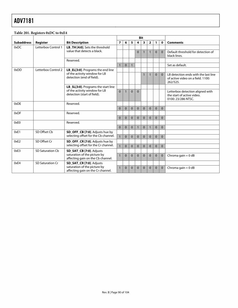
ADV7181
Rev. B | Page 90 of 104
Table 201. Registers 0xDC to 0xE4 Bit
Subaddress Register Bit Description 7 6 5 4 3 2 1 0 Comments LB_TH [4:0]. Sets the threshold
value that detects a black. 0 1 1 0 0 Default threshold for detection of black lines.
0xDC Letterbox Control 1
Reserved.
1 0 1 Set as default.
LB_EL[3:0]. Programs the end line of the activity window for LB detection (end of field).
1 1 0 0 LB detection ends with the last line of active video on a field. 1100: 262/525.
0xDD Letterbox Control 2
LB_SL[3:0]. Programs the start line of the activity window for LB detection (start of field).
0 1 0 0 Letterbox detection aligned with the start of active video. 0100: 23/286 NTSC.
0xDE Reserved.
0 0 0 0 0 0 0 0
0xDF Reserved.
0 0 0 0 0 0 0 0
0xE0 Reserved.
0 0 0 1 0 1 0 0
0xE1 SD Offset Cb SD_OFF_CB [7:0]. Adjusts hue by selecting offset for the Cb channel. 1 0 0 0 0 0 0 0
0xE2 SD Offset Cr SD_OFF_CR [7:0]. Adjusts hue by selecting offset for the Cr channel. 1 0 0 0 0 0 0 0
0xE3 SD Saturation Cb SD_SAT_CB [7:0]. Adjusts saturation of the picture by affecting gain on the Cb channel.
1 0 0 0 0 0 0 0 Chroma gain = 0 dB
0xE4 SD Saturation Cr SD_SAT_CR [7:0]. Adjusts saturation of the picture by affecting gain on the Cr channel.
1 0 0 0 0 0 0 0 Chroma gain = 0 dB
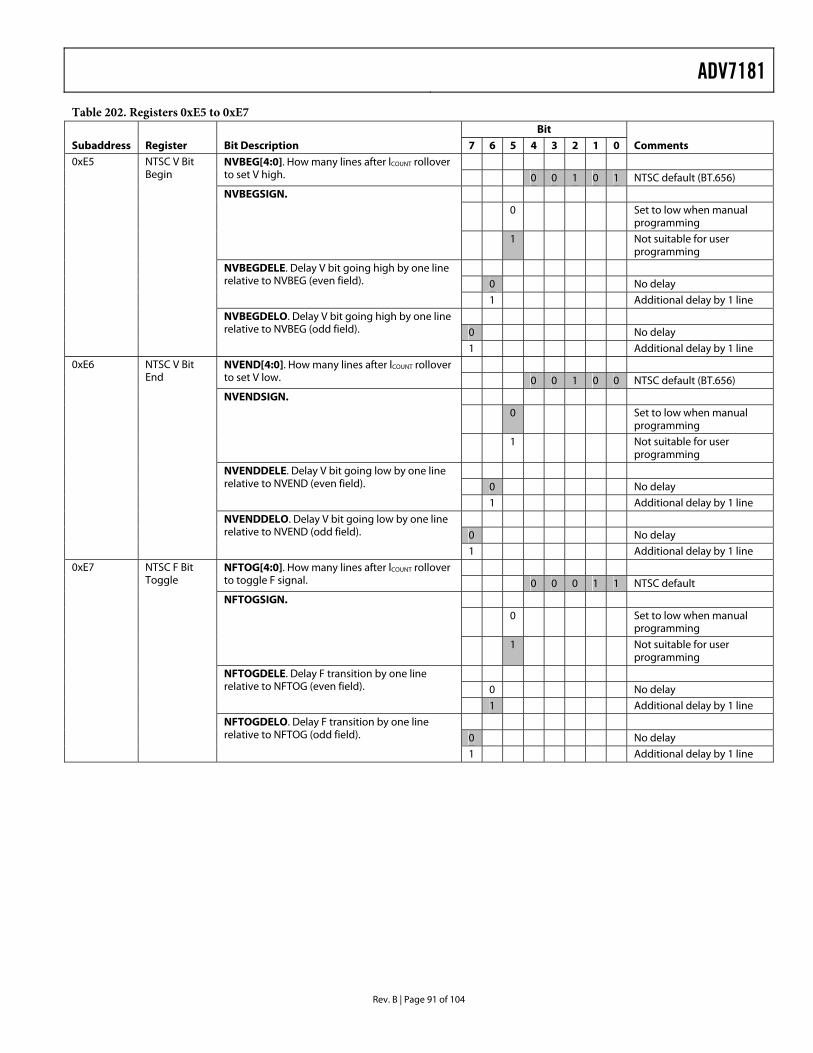
ADV7181
Rev. B | Page 91 of 104
Table 202. Registers 0xE5 to 0xE7 Bit
Subaddress Register Bit Description 7 6 5 4 3 2 1 0 Comments NVBEG[4:0]. How many lines after lCOUNT rollover
to set V high. 0 0 1 0 1 NTSC default (BT.656)
0 Set to low when manual programming
NVBEGSIGN.
1 Not suitable for user programming
0 No delay NVBEGDELE. Delay V bit going high by one line relative to NVBEG (even field).
1 Additional delay by 1 line
0 No delay
0xE5 NTSC V Bit Begin
NVBEGDELO. Delay V bit going high by one line relative to NVBEG (odd field).
1 Additional delay by 1 line
NVEND[4:0]. How many lines after lCOUNT rollover to set V low. 0 0 1 0 0 NTSC default (BT.656)
0 Set to low when manual programming
NVENDSIGN.
1 Not suitable for user programming
0 No delay NVENDDELE. Delay V bit going low by one line relative to NVEND (even field).
1 Additional delay by 1 line
0 No delay
0xE6 NTSC V Bit End
NVENDDELO. Delay V bit going low by one line relative to NVEND (odd field).
1 Additional delay by 1 line
NFTOG[4:0]. How many lines after lCOUNT rollover to toggle F signal. 0 0 0 1 1 NTSC default
0 Set to low when manual programming
NFTOGSIGN.
1 Not suitable for user programming
0 No delay NFTOGDELE. Delay F transition by one line relative to NFTOG (even field).
1 Additional delay by 1 line
0 No delay
0xE7 NTSC F Bit Toggle
NFTOGDELO. Delay F transition by one line relative to NFTOG (odd field).
1 Additional delay by 1 line
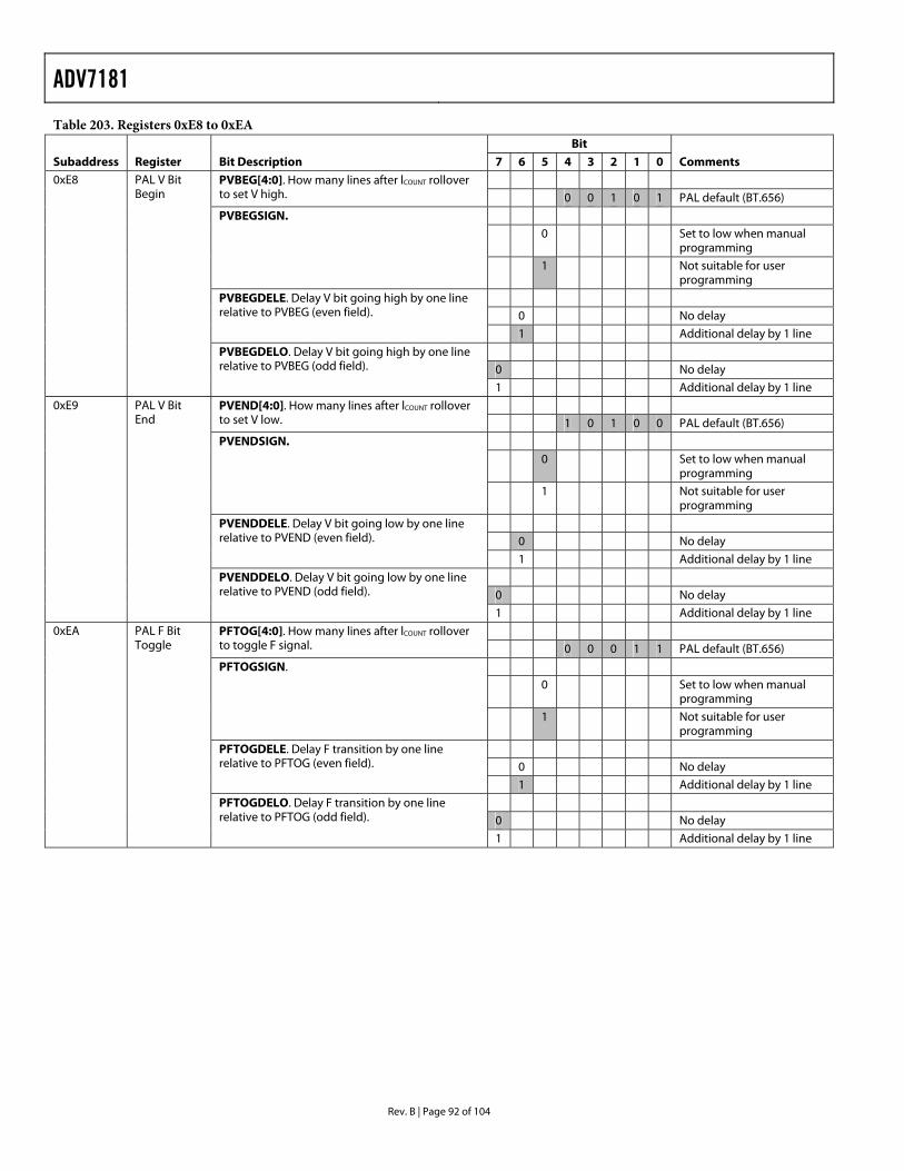
ADV7181
Rev. B | Page 92 of 104
Table 203. Registers 0xE8 to 0xEA Bit
Subaddress Register Bit Description 7 6 5 4 3 2 1 0 Comments PVBEG[4:0]. How many lines after lCOUNT rollover
to set V high. 0 0 1 0 1 PAL default (BT.656)
0 Set to low when manual programming
PVBEGSIGN.
1 Not suitable for user programming
0 No delay PVBEGDELE. Delay V bit going high by one line relative to PVBEG (even field).
1 Additional delay by 1 line
0 No delay
0xE8 PAL V Bit Begin
PVBEGDELO. Delay V bit going high by one line relative to PVBEG (odd field).
1 Additional delay by 1 line
PVEND[4:0]. How many lines after lCOUNT rollover to set V low. 1 0 1 0 0 PAL default (BT.656)
0 Set to low when manual programming
PVENDSIGN.
1 Not suitable for user programming
0 No delay PVENDDELE. Delay V bit going low by one line relative to PVEND (even field).
1 Additional delay by 1 line
0 No delay
0xE9 PAL V Bit End
PVENDDELO. Delay V bit going low by one line relative to PVEND (odd field).
1 Additional delay by 1 line
PFTOG[4:0]. How many lines after lCOUNT rollover to toggle F signal. 0 0 0 1 1 PAL default (BT.656)
0 Set to low when manual programming
PFTOGSIGN.
1 Not suitable for user programming
0 No delay PFTOGDELE. Delay F transition by one line relative to PFTOG (even field).
1 Additional delay by 1 line
0 No delay
0xEA PAL F Bit Toggle
PFTOGDELO. Delay F transition by one line relative to PFTOG (odd field).
1 Additional delay by 1 line
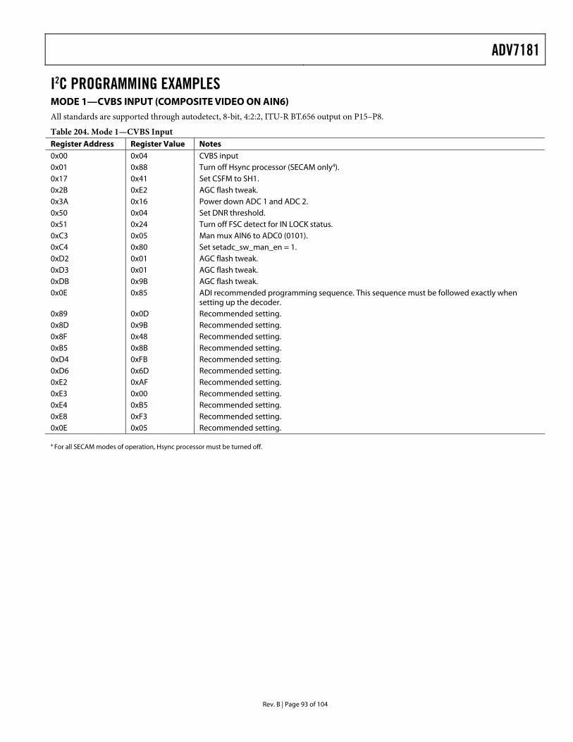
ADV7181
Rev. B | Page 93 of 104
I2C PROGRAMMING EXAMPLES MODE 1—CVBS INPUT (COMPOSITE VIDEO ON AIN6) All standards are supported through autodetect, 8-bit, 4:2:2, ITU-R BT.656 output on P15–P8.
Table 204. Mode 1—CVBS Input Register Address Register Value Notes
0x00 0x04 CVBS input 0x01 0x88 Turn off Hsync processor (SECAM only4). 0x17 0x41 Set CSFM to SH1. 0x2B 0xE2 AGC flash tweak. 0x3A 0x16 Power down ADC 1 and ADC 2. 0x50 0x04 Set DNR threshold. 0x51 0x24 Turn off FSC detect for IN LOCK status. 0xC3 0x05 Man mux AIN6 to ADC0 (0101). 0xC4 0x80 Set setadc_sw_man_en = 1. 0xD2 0x01 AGC flash tweak. 0xD3 0x01 AGC flash tweak. 0xDB 0x9B AGC flash tweak. 0x0E 0x85 ADI recommended programming sequence. This sequence must be followed exactly when
setting up the decoder. 0x89 0x0D Recommended setting. 0x8D 0x9B Recommended setting. 0x8F 0x48 Recommended setting. 0xB5 0x8B Recommended setting. 0xD4 0xFB Recommended setting. 0xD6 0x6D Recommended setting. 0xE2 0xAF Recommended setting. 0xE3 0x00 Recommended setting. 0xE4 0xB5 Recommended setting. 0xE8 0xF3 Recommended setting. 0x0E 0x05 Recommended setting.
4 For all SECAM modes of operation, Hsync processor must be turned off.
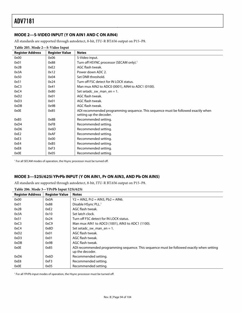
ADV7181
Rev. B | Page 94 of 104
MODE 2—S-VIDEO INPUT (Y ON AIN1 AND C ON AIN4) All standards are supported through autodetect, 8-bit, ITU-R BT.656 output on P15–P8.
Table 205. Mode 2—S-Video Input Register Address Register Value Notes 0x00 0x06 S-Video input. 0x01 0x88 Turn off HSYNC processor (SECAM only).1 0x2B 0xE2 AGC flash tweak. 0x3A 0x12 Power down ADC 2. 0x50 0x04 Set DNR threshold. 0x51 0x24 Turn off FSC detect for IN LOCK status. 0xC3 0x41 Man mux AIN2 to ADC0 (0001), AIN4 to ADC1 (0100). 0xC4 0x80 Set setadc_sw_man_en = 1. 0xD2 0x01 AGC flash tweak. 0xD3 0x01 AGC flash tweak. 0xDB 0x9B AGC flash tweak. 0x0E 0x85 ADI recommended programming sequence. This sequence must be followed exactly when
setting up the decoder. 0xB5 0x8B Recommended setting. 0xD4 0xFB Recommended setting. 0xD6 0x6D Recommended setting. 0xE2 0xAF Recommended setting. 0xE3 0x00 Recommended setting. 0xE4 0xB5 Recommended setting. 0xE8 0xF3 Recommended setting. 0x0E 0x05 Recommended setting.
1 For all SECAM modes of operation, the Hsync processor must be turned off.
MODE 3—525i/625i YPrPb INPUT (Y ON AIN1, Pr ON AIN3, AND Pb ON AIN5) All standards are supported through autodetect, 8-bit, ITU-R BT.656 output on P15–P8.
Table 206. Mode 3—YPrPb Input 525i/625i Register Address Register Value Notes 0x00 0x0A Y2 = AIN2, Pr2 = AIN3, Pb2 = AIN6. 0x01 0x88 Disable HSync PLL.1 0x2B 0xE2 AGC flash tweak. 0x3A 0x10 Set latch clock. 0x51 0x24 Turn off FSC detect for IN LOCK status. 0xC3 0xC9 Man mux AIN1 to ADC0 (1001), AIN3 to ADC1 (1100). 0xC4 0x8D Set setadc_sw_man_en = 1. 0xD2 0x01 AGC flash tweak. 0xD3 0x01 AGC flash tweak. 0xDB 0x9B AGC flash tweak. 0x0E 0x85 ADI recommended programming sequence. This sequence must be followed exactly when setting
up the decoder. 0xD6 0x6D Recommended setting. 0xE8 0xF3 Recommended setting. 0x0E 0x05 Recommended setting.
1 For all YPrPb input modes of operation, the Hsync processor must be turned off.
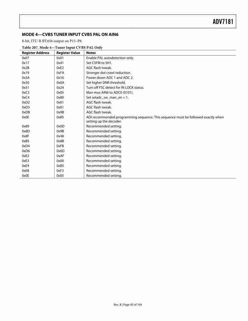
ADV7181
Rev. B | Page 95 of 104
MODE 4—CVBS TUNER INPUT CVBS PAL ON AIN6 8-bit, ITU-R BT.656 output on P15–P8.
Table 207. Mode 4—Tuner Input CVBS PAL Only Register Address Register Value Notes 0x07 0x01 Enable PAL autodetection only. 0x17 0x41 Set CSFM to SH1. 0x2B 0xE2 AGC flash tweak. 0x19 0xFA Stronger dot crawl reduction. 0x3A 0x16 Power down ADC 1 and ADC 2. 0x50 0x0A Set higher DNR threshold. 0x51 0x24 Turn off FSC detect for IN LOCK status. 0xC3 0x05 Man mux AIN6 to ADC0 (0101). 0xC4 0x80 Set setadc_sw_man_en = 1. 0xD2 0x01 AGC flash tweak. 0xD3 0x01 AGC flash tweak. 0xDB 0x9B AGC flash tweak. 0x0E 0x85 ADI recommended programming sequence. This sequence must be followed exactly when
setting up the decoder. 0x89 0x0D Recommended setting. 0x8D 0x9B Recommended setting. 0x8F 0x48 Recommended setting. 0xB5 0x8B Recommended setting. 0xD4 0xFB Recommended setting. 0xD6 0x6D Recommended setting. 0xE2 0xAF Recommended setting. 0xE3 0x00 Recommended setting. 0xE4 0xB5 Recommended setting. 0xE8 0xF3 Recommended setting. 0x0E 0x05 Recommended setting.
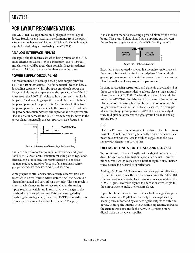
ADV7181
Rev. B | Page 96 of 104
PCB LAYOUT RECOMMENDATIONS The ADV7181 is a high precision, high speed mixed-signal device. To achieve the maximum performance from the part, it is important to have a well laid out PCB board. The following is a guide for designing a board using the ADV7181.
ANALOG INTERFACE INPUTS The inputs should receive care when being routed on the PCB. Track lengths should be kept to a minimum, and 75 Ω trace impedances should be used when possible. Trace impedances other than 75 Ω also increase the chance of reflections.
POWER SUPPLY DECOUPLING It is recommended to decouple each power supply pin with 0.1 µF and 10 nF capacitors. The fundamental idea is to have a decoupling capacitor within about 0.5 cm of each power pin. Also, avoid placing the capacitor on the opposite side of the PC board from the ADV7181; doing so interposes resistive vias in the path. The decoupling capacitors should be located between the power plane and the power pin. Current should flow from the power plane to the capacitor to the power pin. Do not make the power connection between the capacitor and the power pin. Placing a via underneath the 100 nF capacitor pads, down to the power plane, is generally the best approach (see Figure 37).
0482
0-03
8
VDD
GND10nF 100nF
VIA TO SUPPLY
VIA TO GND
Figure 37. Recommend Power Supply Decoupling
It is particularly important to maintain low noise and good stability of PVDD. Careful attention must be paid to regulation, filtering, and decoupling. It is highly desirable to provide separate regulated supplies for each of the analog circuitry groups (AVDD, DVDD, DVDDIO, and PVDD).
Some graphic controllers use substantially different levels of power when active (during active picture time) and when idle (during horizontal and vertical sync periods). This can result in a measurable change in the voltage supplied to the analog supply regulator, which can, in turn, produce changes in the regulated analog supply voltage. This can be mitigated by regulating the analog supply, or at least PVDD, from a different, cleaner, power source, for example, from a 12 V supply.
It is also recommend to use a single ground plane for the entire board. This ground plane should have a spacing gap between the analog and digital sections of the PCB (see Figure 38).
0482
0-03
7
ANALOGSECTION
DIGITALSECTION
ADV7181
Figure 38. PCB Ground Layout
Experience has repeatedly shown that the noise performance is the same or better with a single ground plane. Using multiple ground planes can be detrimental because each separate ground plane is smaller, and long ground loops can result.
In some cases, using separate ground planes is unavoidable. For those cases, it is recommended to at least place a single ground plane under the ADV7181. The location of the split should be under the ADV7181. For this case, it is even more important to place components wisely because the current loops are much longer (current takes the path of least resistance). An example of a current loop: power plane to ADV7181 to digital output trace to digital data receiver to digital ground plane to analog ground plane.
PLL Place the PLL loop filter components as close to the ELPF pin as possible. Do not place any digital or other high frequency traces near these components. Use the values suggested in the data sheet with tolerances of 10% or less.
DIGITAL OUTPUTS (BOTH DATA AND CLOCKS) Try to minimize the trace length that the digital outputs have to drive. Longer traces have higher capacitance, which requires more current, which causes more internal digital noise. Shorter traces reduce the possibility of reflections.
Adding a 30 Ω and 50 Ω series resistor can suppress reflections, reduce EMI, and reduce the current spikes inside the ADV7181. If series resistors are used, place them as close as possible to the ADV7181 pins. However, try not to add vias or extra length to the output trace to make the resistors closer.
If possible, limit the capacitance that each of the digital outputs drives to less than 15 pF. This can easily be accomplished by keeping traces short and by connecting the outputs to only one device. Loading the outputs with excessive capacitance increases the current transients inside the ADV7181, creating more digital noise on its power supplies.
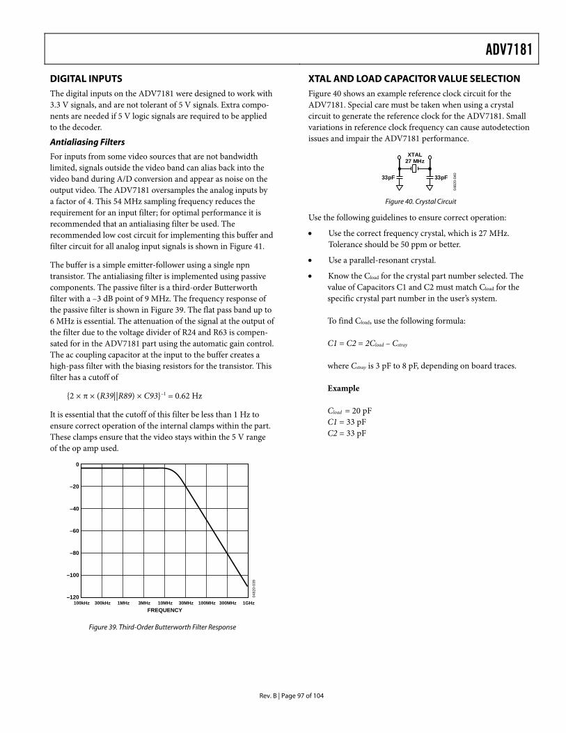
ADV7181
Rev. B | Page 97 of 104
DIGITAL INPUTS The digital inputs on the ADV7181 were designed to work with 3.3 V signals, and are not tolerant of 5 V signals. Extra compo-nents are needed if 5 V logic signals are required to be applied to the decoder.
Antialiasing Filters
For inputs from some video sources that are not bandwidth limited, signals outside the video band can alias back into the video band during A/D conversion and appear as noise on the output video. The ADV7181 oversamples the analog inputs by a factor of 4. This 54 MHz sampling frequency reduces the requirement for an input filter; for optimal performance it is recommended that an antialiasing filter be used. The recommended low cost circuit for implementing this buffer and filter circuit for all analog input signals is shown in Figure 41.
The buffer is a simple emitter-follower using a single npn transistor. The antialiasing filter is implemented using passive components. The passive filter is a third-order Butterworth filter with a –3 dB point of 9 MHz. The frequency response of the passive filter is shown in Figure 39. The flat pass band up to 6 MHz is essential. The attenuation of the signal at the output of the filter due to the voltage divider of R24 and R63 is compen-sated for in the ADV7181 part using the automatic gain control. The ac coupling capacitor at the input to the buffer creates a high-pass filter with the biasing resistors for the transistor. This filter has a cutoff of
2 × π × (R39||R89) × C93–1 = 0.62 Hz
It is essential that the cutoff of this filter be less than 1 Hz to ensure correct operation of the internal clamps within the part. These clamps ensure that the video stays within the 5 V range of the op amp used.
0
–20
–40
–60
–80
–100
–120100kHz 30MHz10MHz3MHz1MHz300kHz 300MHz 1GHz100MHz
0482
0-03
9
FREQUENCY
Figure 39. Third-Order Butterworth Filter Response
XTAL AND LOAD CAPACITOR VALUE SELECTION Figure 40 shows an example reference clock circuit for the ADV7181. Special care must be taken when using a crystal circuit to generate the reference clock for the ADV7181. Small variations in reference clock frequency can cause autodetection issues and impair the ADV7181 performance.
33pF 33pF
XTAL27 MHz
0482
0-04
0
Figure 40. Crystal Circuit
Use the following guidelines to ensure correct operation:
• Use the correct frequency crystal, which is 27 MHz. Tolerance should be 50 ppm or better.
• Use a parallel-resonant crystal.
• Know the Cload for the crystal part number selected. The value of Capacitors C1 and C2 must match Cload for the specific crystal part number in the user’s system. To find Cload, use the following formula: C1 = C2 = 2Cload – Cstray where Cstray is 3 pF to 8 pF, depending on board traces. Example Cload = 20 pF C1 = 33 pF C2 = 33 pF
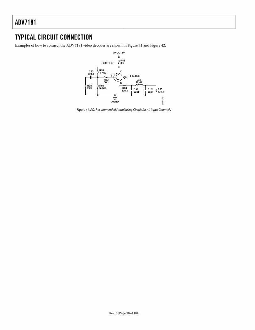
ADV7181
Rev. B | Page 98 of 104
TYPICAL CIRCUIT CONNECTION Examples of how to connect the ADV7181 video decoder are shown in Figure 41 and Figure 42.
0482
0-04
2
BQ6
C
ER3875Ω
R895.6kΩ R63
820Ω
R430Ω
R5356Ω
R24470Ω
R394.7kΩ
C9522pF
C10210pF
C93100µF
AVDD_5V
L1012µH
FILTER
BUFFER
AGND
Figure 41. ADI Recommended Antialiasing Circuit for All Input Channels
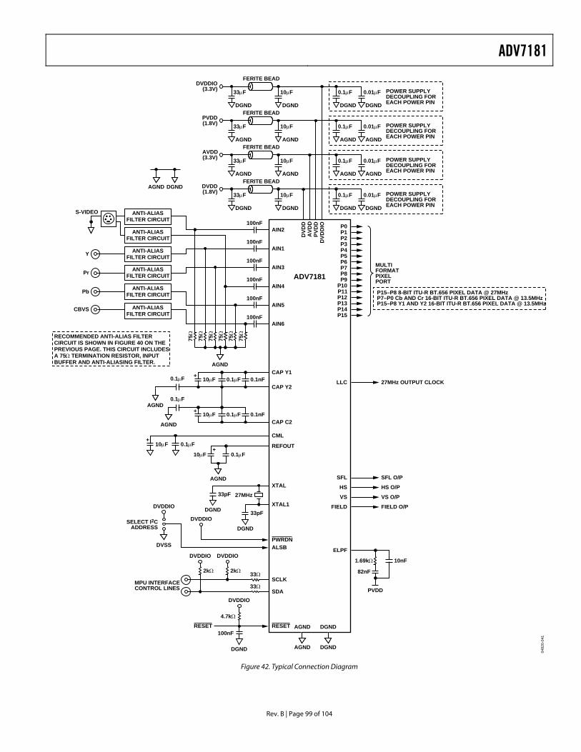
ADV7181
Rev. B | Page 99 of 104
0482
0-04
1
2kΩ 2kΩ
AGND DGND
AGND DGND
0.1µF
DGND
0.01µF
DGND
33µF
DGND
10µF
DGND
FERITE BEADDVDDIO
(3.3V) POWER SUPPLYDECOUPLING FOREACH POWER PIN
0.1µF
AGND
0.01µF
AGND
33µF
AGND
10µF
AGND
FERITE BEADPVDD(1.8V) POWER SUPPLY
DECOUPLING FOREACH POWER PIN
0.1µF
AGND
0.01µF
AGND
33µF
AGND
10µF
AGND
FERITE BEADAVDD(3.3V) POWER SUPPLY
DECOUPLING FOREACH POWER PIN
0.1µF
DGND
0.01µF
DGND
33µF
DGND
10µF
DGND
FERITE BEADDVDD(1.8V) POWER SUPPLY
DECOUPLING FOREACH POWER PIN
AGND DGND
DVD
DA
VDD
PVD
DD
VDD
IO
AIN2100nF
AIN1100nF
AIN3100nF
AIN4100nF
AIN5100nF
AIN6100nF
AGND
75Ω
75Ω
75Ω
75Ω
75Ω
75Ω
S-VIDEO
Y
Pr
Pb
CBVS
+ CAP Y1
CAP Y2
AGND
0.1µF10µF0.1µF
+
CAP C2
CML
AGND
0.1µF
0.1nF
0.1nF10µF
0.1µF
LLC 27MHz OUTPUT CLOCK
SFL SFL O/P
HS HS O/P
VS VS O/P
FIELD FIELD O/P
ELPF
1.69kΩ 10nF
82nF
PVDD
DGND
DVDDIO
100nF
P15–P8 8-BIT ITU-R BT.656 PIXEL DATA @ 27MHzP7–P0 Cb AND Cr 16-BIT ITU-R BT.656 PIXEL DATA @ 13.5MHzP15–P8 Y1 AND Y2 16-BIT ITU-R BT.656 PIXEL DATA @ 13.5MHz
P0P1P2P3P4P5P6P7P8P9
P10P11P12P13P14P15
MULTIFORMATPIXELPORT
+10µF 0.1µF REFOUT
AGND
0.1µF10µF+
XTAL33pF
DGNDXTAL1
ALSB
33pF
DGND
27MHz
ADV7181
DVDDIO
DVDDIOSELECT I2CADDRESS
DVSSPWRDN
MPU INTERFACECONTROL LINES
SCLK
SDA
33Ω
33Ω
DVDDIO DVDDIO
4.7kΩ
RESETRESET
ANTI-ALIASFILTER CIRCUIT
ANTI-ALIASFILTER CIRCUIT
ANTI-ALIASFILTER CIRCUIT
ANTI-ALIASFILTER CIRCUIT
ANTI-ALIASFILTER CIRCUIT
ANTI-ALIASFILTER CIRCUIT
RECOMMENDED ANTI-ALIAS FILTERCIRCUIT IS SHOWN IN FIGURE 40 ON THEPREVIOUS PAGE. THIS CIRCUIT INCLUDESA 75Ω TERMINATION RESISTOR, INPUTBUFFER AND ANTI-ALIASING FILTER.
Figure 42. Typical Connection Diagram
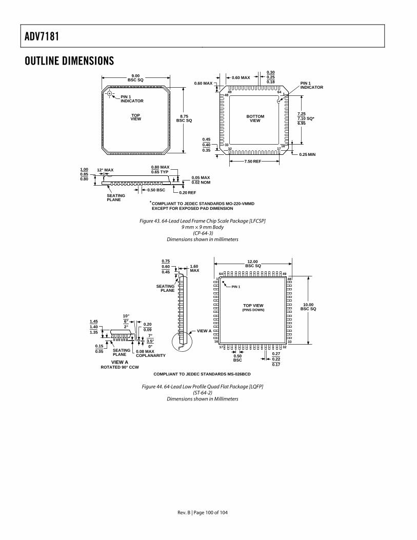
ADV7181
Rev. B | Page 100 of 104
OUTLINE DIMENSIONS
164
1617
4948
3233
0.450.400.35
0.60 MAX0.60 MAX
0.25 MIN
0.50 BSC 0.20 REF
*COMPLIANT TO JEDEC STANDARDS MO-220-VMMDEXCEPT FOR EXPOSED PAD DIMENSION
BOTTOMVIEW
0.300.250.18
7.50 REF
7.257.10 SQ*6.95
12° MAX0.80 MAX0.65 TYP1.00
0.850.80 0.05 MAX
0.02 NOM
SEATINGPLANE
TOPVIEW
9.00BSC SQ
8.75BSC SQ
PIN 1INDICATOR
PIN 1INDICATOR
Figure 43. 64-Lead Lead Frame Chip Scale Package [LFCSP] 9 mm × 9 mm Body
(CP-64-3) Dimensions shown in millimeters
TOP VIEW(PINS DOWN)
1
1617
3332
484964
0.270.220.17
0.50BSC
10.00BSC SQ
1.60MAX
SEATINGPLANE
0.750.600.45
VIEW A
12.00BSC SQ
0.20 0.09
1.45 1.40 1.35
0.08 MAXCOPLANARITY
VIEW AROTATED 90° CCW
SEATINGPLANE
10°6°2°
7°3.5°0°0.15
0.05
PIN 1
COMPLIANT TO JEDEC STANDARDS MS-026BCD
Figure 44. 64-Lead Low Profile Quad Flat Package [LQFP] (ST-64-2)
Dimensions shown in Millimeters
ADV7181
Rev. B | Page 101 of 104
ORDERING GUIDE Model Temperature Range Package Description Package Option ADV7181BCP –40°C to +85°C Lead Frame Chip Scale Package (LFCSP) CP-64-3 ADV7181BST –40°C to +85°C Low Profile Quad Flat Package (LQFP) ST-64-2 EVAL-ADV7181BEB Evaluation Board
The ADV7181 is a Pb-free environmentally friendly product. It is manufactured using the most up-to-date materials and processes. The coating on the leads of each device is 100% pure Sn electroplate. The device is suitable for Pb-free applications, and can withstand surface-mount soldering at up to 255°C (±5°C).
In addition, it is backward-compatible with conventional SnPb soldering processes. This means the electroplated Sn coating can be soldered with Sn/Pb solder pastes at conventional reflow temperatures of 220°C to 235°C.
The ADV7181 evaluation board is now obsolete. For new evaluation and design, the ADV7181B evaluation board is recommended.

ADV7181
Rev. B | Page 102 of 104
NOTES

ADV7181
Rev. B | Page 103 of 104
NOTES

ADV7181
Rev. B | Page 104 of 104
NOTES
Purchase of licensed I2C components of Analog Devices or one of its sublicensed Associated Companies conveys a license for the purchaser under the Philips I2C Patent Rights to use these components in an I2C system, provided that the system conforms to the I2C Standard Specification as defined by Philips.
© 2005 Analog Devices, Inc. All rights reserved. Trademarks and registered trademarks are the property of their respective owners. D04820–0–3/05(B)