modern control regulator design for dc-dc …web.cecs.pdx.edu/~tymerski/ece451/cuk_control.pdfmodern...
TRANSCRIPT
Modern Control Regulator Design
for DC-DC Converters
Franklin J. Rytkonen and Dr. Richard Tymerski
Electrical and Computer Engineering Department
Portland State University
Chapter 1
System Analysis
Prior to designing a controller for a system, the control system designer must understand the character-istics of the system. For example, is the system open-loop stable? Are there dominant poles, or poles thatmay be neglected during design? Is the system controllable using the selected inputs? Can an estimator beconstructed based on the measured outputs? These types of questions should be answered both intuitivelyand mathematically prior to embarking on an attempt to design a controller for the system. For example,the compensator design process for the Cuk converter begins with the construction of a mathematical modelof the system in MATLAB (The Mathworks, Inc.). The model is a mathematical description of some orall of the behavior of the real-world system that is adequate for performing controller design. State spaceaveraging yields a linear small-signal model for the nonlinear switching system (derivations may be foundin the Appendix) [1]. Additionally, a nonlinear circuit model was created in the Power Electronics CircuitSimulator (PECS) software package in order to validate the performance of the linear model. PECS uses aschematic-based circuit editor and features its own plotting tool, PECSPLOT.
1.1 The Cuk Converter
The Cuk converter is a step-down/step-up converter based on a switching boost-buck topology. Essen-tially, the converter is composed of two sections, an input stage and an output stage. The schematic of theCuk converter is presented in Figure 1.1, with component values given in the Appendix. (The lowercase vari-ables indicate small-signal deviations from nominal operating point variables as obtained by linearization.)The input voltage vg is fed into the circuit via inductor L1. When transistor Q1 is on, current i1 builds themagnetic field of the inductor in the input stage. The diode CR1 is reverse biased, and energy dissipatesfrom the storage elements in the output stage. When Q1 turns off, inductor L1 tries to maintain the currentflowing through it by reversing polarity and sourcing current as its magnetic field collapses. It thus providesenergy to the output stage of the circuit via capacitor C1. Both currents i1 and i2 must sum to zero in thesteady state, since the assumption is that voltage v1 is essentially constant (given that the voltage across acapacitor cannot change instantaneously and the switching speed of the circuit is high). This provides forthe following relation:
i1ton + i2toff = 0 (1.1)
The inductor currents are the input and output currents, therefore, if the principle of conservation of energyis applied:
vo
vg=
Ds
1−Ds
(1.2)
where Ds is the duty cycle of the switch, Ds∆= ton
ton+toff. Thus, the voltage ratio of a Cuk converter is the
same as that of a buck-boost converter, but its main advantage over other converters is that the input andoutput inductors result in a filtered current on both sides of the converter, while buck, boost, and buck-boost
1
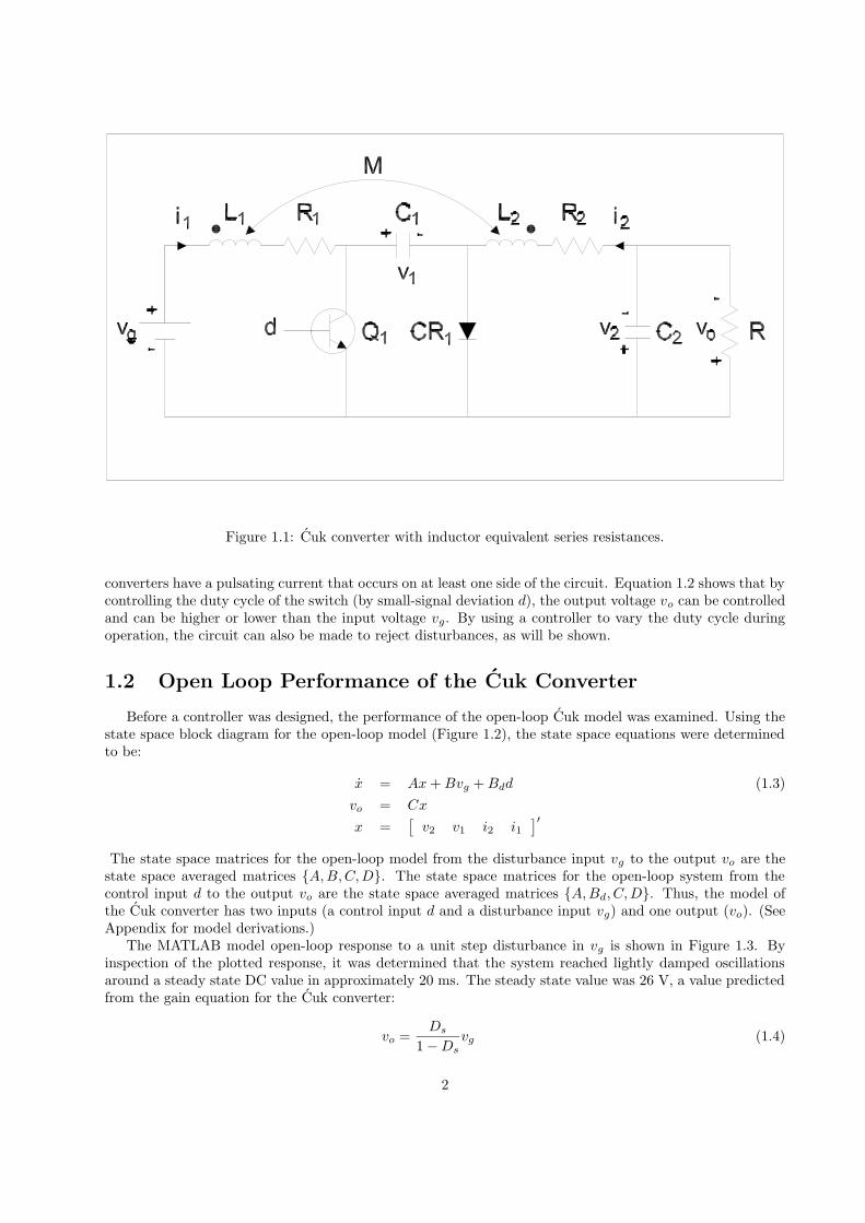
Figure 1.1: Cuk converter with inductor equivalent series resistances.
converters have a pulsating current that occurs on at least one side of the circuit. Equation 1.2 shows that bycontrolling the duty cycle of the switch (by small-signal deviation d), the output voltage vo can be controlledand can be higher or lower than the input voltage vg. By using a controller to vary the duty cycle duringoperation, the circuit can also be made to reject disturbances, as will be shown.
1.2 Open Loop Performance of the Cuk Converter
Before a controller was designed, the performance of the open-loop Cuk model was examined. Using thestate space block diagram for the open-loop model (Figure 1.2), the state space equations were determinedto be:
x = Ax+Bvg +Bdd (1.3)
vo = Cx
x =[
v2 v1 i2 i1]
′
The state space matrices for the open-loop model from the disturbance input vg to the output vo are thestate space averaged matrices A,B,C,D. The state space matrices for the open-loop system from thecontrol input d to the output vo are the state space averaged matrices A,Bd, C,D. Thus, the model ofthe Cuk converter has two inputs (a control input d and a disturbance input vg) and one output (vo). (SeeAppendix for model derivations.)
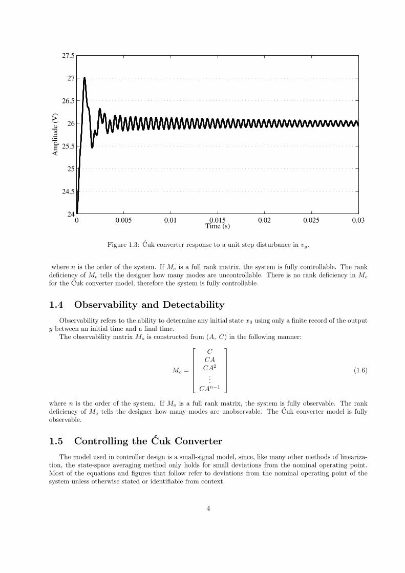
The MATLAB model open-loop response to a unit step disturbance in vg is shown in Figure 1.3. Byinspection of the plotted response, it was determined that the system reached lightly damped oscillationsaround a steady state DC value in approximately 20 ms. The steady state value was 26 V, a value predictedfrom the gain equation for the Cuk converter:
vo =Ds
1−Ds
vg (1.4)
2
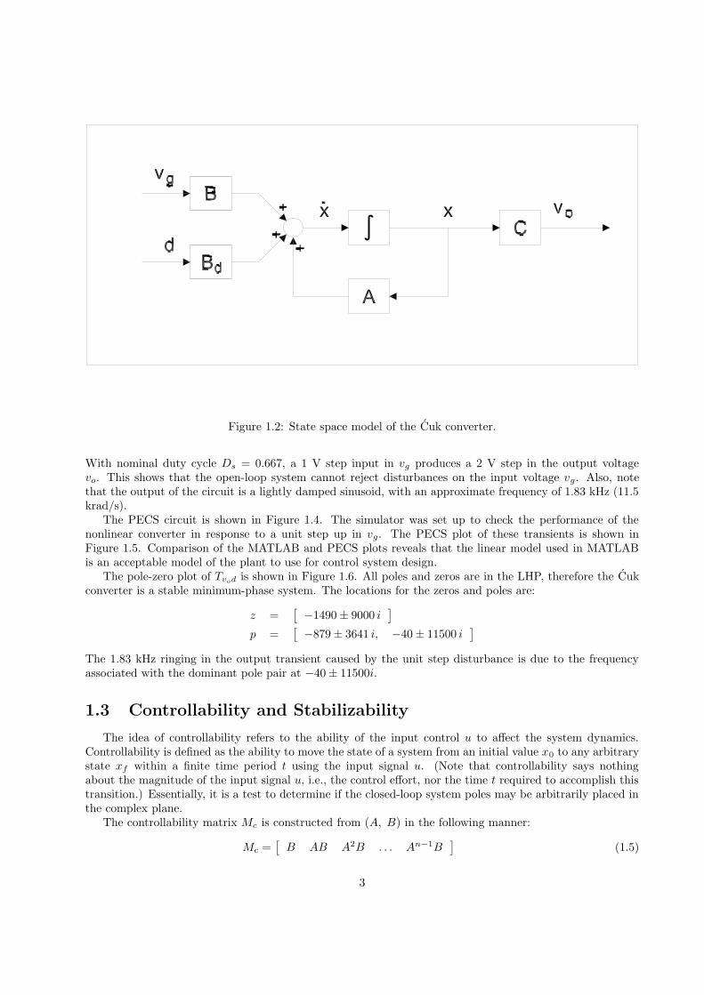
Figure 1.2: State space model of the Cuk converter.
With nominal duty cycle Ds = 0.667, a 1 V step input in vg produces a 2 V step in the output voltagevo. This shows that the open-loop system cannot reject disturbances on the input voltage vg. Also, notethat the output of the circuit is a lightly damped sinusoid, with an approximate frequency of 1.83 kHz (11.5krad/s).
The PECS circuit is shown in Figure 1.4. The simulator was set up to check the performance of thenonlinear converter in response to a unit step up in vg. The PECS plot of these transients is shown inFigure 1.5. Comparison of the MATLAB and PECS plots reveals that the linear model used in MATLABis an acceptable model of the plant to use for control system design.
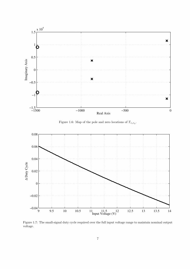
The pole-zero plot of Tvod is shown in Figure 1.6. All poles and zeros are in the LHP, therefore the Cukconverter is a stable minimum-phase system. The locations for the zeros and poles are:
z =[
−1490± 9000 i]
p =[
−879± 3641 i, −40± 11500 i]
The 1.83 kHz ringing in the output transient caused by the unit step disturbance is due to the frequencyassociated with the dominant pole pair at −40± 11500i.
1.3 Controllability and Stabilizability
The idea of controllability refers to the ability of the input control u to affect the system dynamics.Controllability is defined as the ability to move the state of a system from an initial value x0 to any arbitrarystate xf within a finite time period t using the input signal u. (Note that controllability says nothingabout the magnitude of the input signal u, i.e., the control effort, nor the time t required to accomplish thistransition.) Essentially, it is a test to determine if the closed-loop system poles may be arbitrarily placed inthe complex plane.
The controllability matrix Mc is constructed from (A, B) in the following manner:
Mc =[
B AB A2B . . . An−1B]
(1.5)
3
0 0.005 0.01 0.015 0.02 0.025 0.0324
24.5
25
25.5
26
26.5
27
27.5
Time (s)
Am
plitu
de (V
)
Figure 1.3: Cuk converter response to a unit step disturbance in vg.
where n is the order of the system. If Mc is a full rank matrix, the system is fully controllable. The rankdeficiency of Mc tells the designer how many modes are uncontrollable. There is no rank deficiency in Mc
for the Cuk converter model, therefore the system is fully controllable.
1.4 Observability and Detectability
Observability refers to the ability to determine any initial state x0 using only a finite record of the outputy between an initial time and a final time.
The observability matrix Mo is constructed from (A, C) in the following manner:
Mo =
C
CA
CA2
...CAn−1
(1.6)
where n is the order of the system. If Mo is a full rank matrix, the system is fully observable. The rankdeficiency of Mo tells the designer how many modes are unobservable. The Cuk converter model is fullyobservable.
1.5 Controlling the Cuk Converter
The model used in controller design is a small-signal model, since, like many other methods of lineariza-tion, the state-space averaging method only holds for small deviations from the nominal operating point.Most of the equations and figures that follow refer to deviations from the nominal operating point of thesystem unless otherwise stated or identifiable from context.
4
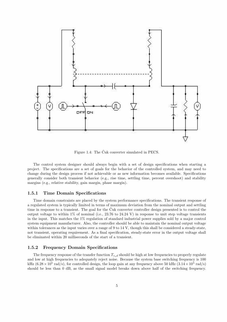
Figure 1.4: The Cuk converter simulated in PECS.
The control system designer should always begin with a set of design specifications when starting aproject. The specifications are a set of goals for the behavior of the controlled system, and may need tochange during the design process if not achievable or as new information becomes available. Specificationsgenerally consider both transient behavior (e.g., rise time, settling time, percent overshoot) and stabilitymargins (e.g., relative stability, gain margin, phase margin).
1.5.1 Time Domain Specifications
Time domain constraints are placed by the system performance specifications. The transient response ofa regulated system is typically limited in terms of maximum deviation from the nominal output and settlingtime in response to a transient. The goal for the Cuk converter controller design presented is to control theoutput voltage to within 1% of nominal (i.e., 23.76 to 24.24 V) in response to unit step voltage transientsin the input. This matches the 1% regulation of standard industrial power supplies sold by a major controlsystem equipment manufacturer. Also, the controller should be able to maintain the nominal output voltagewithin tolerances as the input varies over a range of 9 to 14 V, though this shall be considered a steady-state,not transient, operating requirement. As a final specification, steady-state error in the output voltage shallbe eliminated within 20 milliseconds of the start of a transient.
1.5.2 Frequency Domain Specifications
The frequency response of the transfer function Tvod should be high at low frequencies to properly regulateand low at high frequencies to adequately reject noise. Because the system base switching frequency is 100kHz (6.28×10⁵ rad/s), for controlled design, the loop gain at any frequency above 50 kHz (3.14×10⁵ rad/s)should be less than 0 dB, as the small signal model breaks down above half of the switching frequency.
5
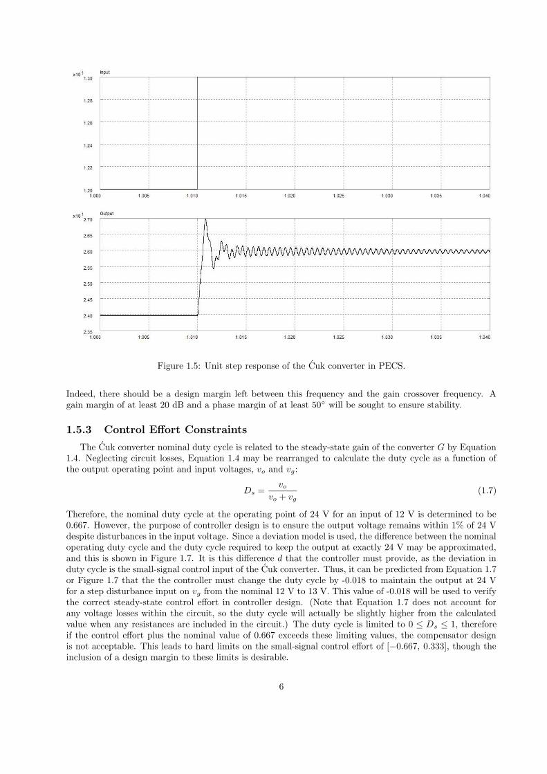
Figure 1.5: Unit step response of the Cuk converter in PECS.
Indeed, there should be a design margin left between this frequency and the gain crossover frequency. Again margin of at least 20 dB and a phase margin of at least 50 will be sought to ensure stability.
1.5.3 Control Effort Constraints
The Cuk converter nominal duty cycle is related to the steady-state gain of the converter G by Equation1.4. Neglecting circuit losses, Equation 1.4 may be rearranged to calculate the duty cycle as a function ofthe output operating point and input voltages, vo and vg:
Ds =vo
vo + vg(1.7)
Therefore, the nominal duty cycle at the operating point of 24 V for an input of 12 V is determined to be0.667. However, the purpose of controller design is to ensure the output voltage remains within 1% of 24 Vdespite disturbances in the input voltage. Since a deviation model is used, the difference between the nominaloperating duty cycle and the duty cycle required to keep the output at exactly 24 V may be approximated,and this is shown in Figure 1.7. It is this difference d that the controller must provide, as the deviation induty cycle is the small-signal control input of the Cuk converter. Thus, it can be predicted from Equation 1.7or Figure 1.7 that the the controller must change the duty cycle by -0.018 to maintain the output at 24 Vfor a step disturbance input on vg from the nominal 12 V to 13 V. This value of -0.018 will be used to verifythe correct steady-state control effort in controller design. (Note that Equation 1.7 does not account forany voltage losses within the circuit, so the duty cycle will actually be slightly higher from the calculatedvalue when any resistances are included in the circuit.) The duty cycle is limited to 0 ≤ Ds ≤ 1, thereforeif the control effort plus the nominal value of 0.667 exceeds these limiting values, the compensator designis not acceptable. This leads to hard limits on the small-signal control effort of [−0.667, 0.333], though theinclusion of a design margin to these limits is desirable.
6
−1500 −1000 −500 0−1.5
−1
−0.5
0
0.5
1
1.5x 10⁴
Imag
inar
y A
xis
Real Axis
Figure 1.6: Map of the pole and zero locations of Tvovg.
9 9.5 10 10.5 11 11.5 12 12.5 13 13.5 14−0.04
−0.02
0
0.02
0.04
0.06
0.08
Input Voltage (V)
∆ D
uty
Cyc
le
Figure 1.7: The small-signal duty cycle required over the full input voltage range to maintain nominal outputvoltage.
7
Chapter 2
Pole Placement
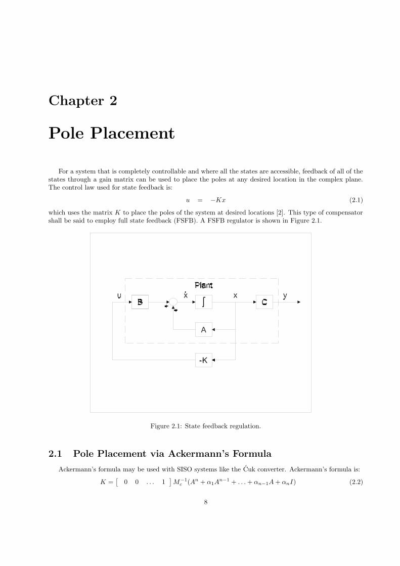
For a system that is completely controllable and where all the states are accessible, feedback of all of thestates through a gain matrix can be used to place the poles at any desired location in the complex plane.The control law used for state feedback is:
u = −Kx (2.1)
which uses the matrix K to place the poles of the system at desired locations [2]. This type of compensatorshall be said to employ full state feedback (FSFB). A FSFB regulator is shown in Figure 2.1.
Figure 2.1: State feedback regulation.
2.1 Pole Placement via Ackermann’s Formula
Ackermann’s formula may be used with SISO systems like the Cuk converter. Ackermann’s formula is:
K =[
0 0 . . . 1]
M−1c (An + α1A
n−1 + . . .+ αn−1A+ αnI) (2.2)
8
This method of determining K may be used with the system in any representation. It is this method of poleplacement that is used in the designs of the state feedback controllers that follow.
2.2 Cuk Converter with State Feedback Compensator
One problem with pole placement is how to go about selecting desirable pole locations. Two mainmethods of design are suggested:
• Select pole locations such that a dominant complex pole pair exists. This technique is generally usedwhen designing tracking systems, for which the transient time domain requirements (e.g., rise time,overshoot, settling time, etc.) are able to be recast into desired dominant pole locations.
• Select pole locations that have been determined to give a prototype time-domain response, e.g., filterpole locations.
The latter method has been selected for use with full state feedback.Graham and Lathrop [3] discuss assigning the system poles of higher-order systems to prototype locations
that minimizes a performance index (or cost function) known as the integral of the time-weighted absoluteerror (ITAE) to an input signal:
JITAE =
∫
∞
0
t |e(t)| dt (2.3)
By placing poles in an ITAE filter pattern to minimize JITAE , the designer achieves a response that isoptimized with respect to deviation from setpoint (provided by the absolute error) and settling time (errorsthat occur later in the time history contribute more to the JITAE cost). Since the goal of the control systemdesigner is to regulate the Cuk converter output voltage with respect to input voltage disturbances, JITAEprovides a scalar figure of merit by which to judge controller performance. For regulator problems, thedesired output is rejection of disturbance deviations from the nominal operating point. The error betweenthe desired output and the plant output is defined as e(t) = r(t) − y(t). Since r(t) = 0 for all time t in aregulator problem, the error e(t) is simply −y(t).
The frequency-normalized characteristic equations for minimum ITAE response are given in Table 2.1 upthrough order five (so that a full-order state feedback controller with an integrator may be applied to theCuk converter).
Table 2.1: Frequency-Normalized Characteristic Equations for ITAE Response
Order Characteristic Equation
1 s+ ω
2 s2 + 1.414ωs+ ω2
3 s3 + 1.75ωs2 + 2.15ω2s+ ω3
4 s4 + 2.1ωs3 + 3.4ω2s2 + 2.7ω3s+ ω4
5 s5 + 2.8ωs4 + 5ω2s3 + 5.5ω3s2 + 3.4ω4s+ ω5
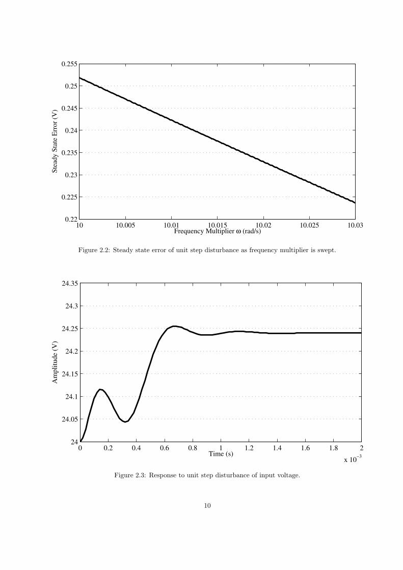
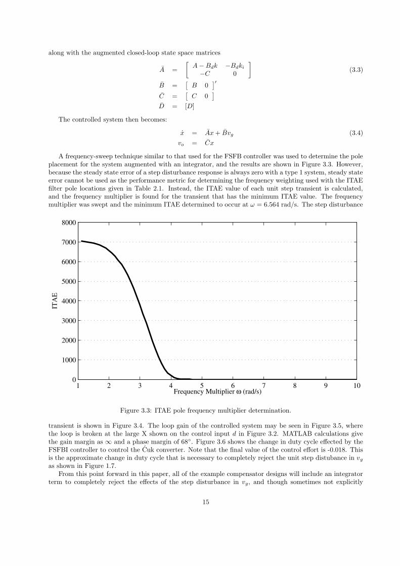
A control system designer can use a computer program (e.g., MATLAB from The Mathworks with theControl Systems Toolbox) to iteratively design and test state feedback controllers over a range of valuesfor ω. It is easiest to work with the characteristic equations given in Table 2.1 in MATLAB in a factoredformat as shown in Table 2.2. The control system designer must determine the value of the scalar multiplierfrequency ω that places the poles in such a way as to achieve the desired time domain response. By using thesteady state error as a measurement metric for each iteration during the design, a frequency multiplier ω canbe chosen that produces a steady state error within the performance specification of 1%. This design methodwas used to select the pole locations for a full state feedback controller as shown in Figure 2.2. Initially, awide range of frequencies was selected with a large increment, then the range and the increment were madesmaller in order to narrow in on the first frequency with less than 0.24 V of steady state error, which occursat ω = 10.0125 rad/s. The unit step disturbance response of the system with a full state feedback controller
9
10 10.005 10.01 10.015 10.02 10.025 10.030.22
0.225
0.23
0.235
0.24
0.245
0.25
0.255
Frequency Multiplier ω (rad/s)
Stea
dy S
tate
Err
or (V
)
Figure 2.2: Steady state error of unit step disturbance as frequency multiplier is swept.
0 0.2 0.4 0.6 0.8 1 1.2 1.4 1.6 1.8 2
x 10−3
24
24.05
24.1
24.15
24.2
24.25
24.3
24.35
Time (s)
Am
plitu
de (V
)
Figure 2.3: Response to unit step disturbance of input voltage.
10
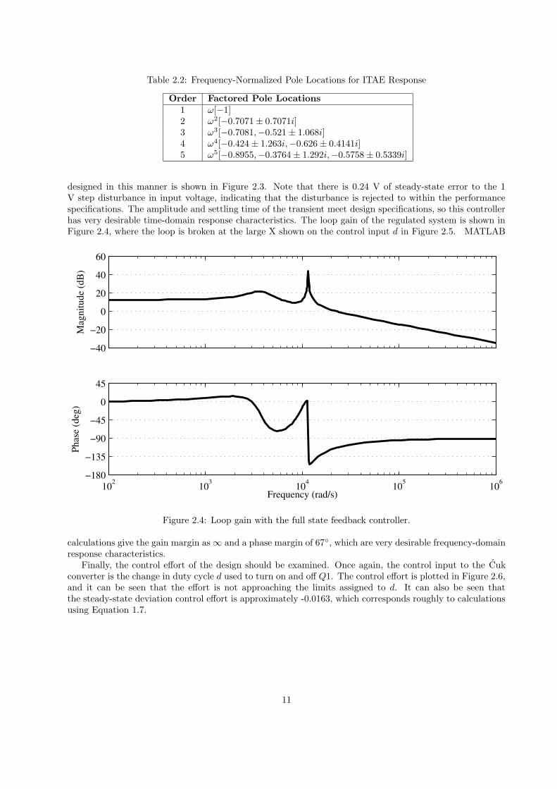
Table 2.2: Frequency-Normalized Pole Locations for ITAE Response
Order Factored Pole Locations
1 ω[−1]2 ω2[−0.7071± 0.7071i]3 ω3[−0.7081,−0.521± 1.068i]4 ω4[−0.424± 1.263i,−0.626± 0.4141i]5 ω5[−0.8955,−0.3764± 1.292i,−0.5758± 0.5339i]
designed in this manner is shown in Figure 2.3. Note that there is 0.24 V of steady-state error to the 1V step disturbance in input voltage, indicating that the disturbance is rejected to within the performancespecifications. The amplitude and settling time of the transient meet design specifications, so this controllerhas very desirable time-domain response characteristics. The loop gain of the regulated system is shown inFigure 2.4, where the loop is broken at the large X shown on the control input d in Figure 2.5. MATLAB
−40
−20
0
20
40
60
Mag
nitu
de (d
B)
102 103 104 105 106−180
−135
−90
−45
0
45
Phas
e (d
eg)
Frequency (rad/s)
Figure 2.4: Loop gain with the full state feedback controller.
calculations give the gain margin as∞ and a phase margin of 67, which are very desirable frequency-domainresponse characteristics.
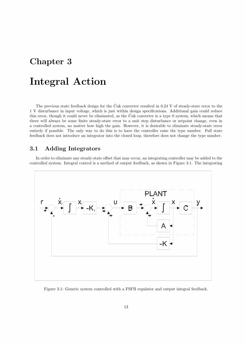
Finally, the control effort of the design should be examined. Once again, the control input to the Cukconverter is the change in duty cycle d used to turn on and off Q1. The control effort is plotted in Figure 2.6,and it can be seen that the effort is not approaching the limits assigned to d. It can also be seen thatthe steady-state deviation control effort is approximately -0.0163, which corresponds roughly to calculationsusing Equation 1.7.
11
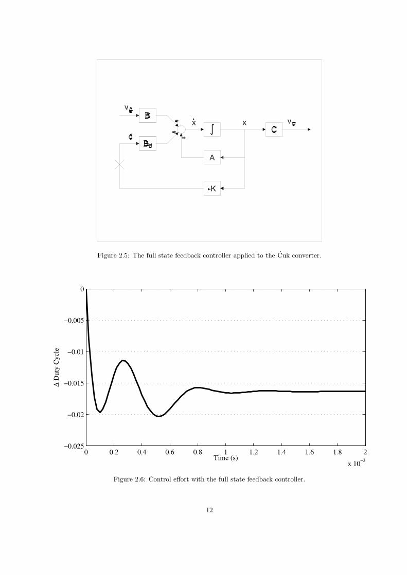
Figure 2.5: The full state feedback controller applied to the Cuk converter.
0 0.2 0.4 0.6 0.8 1 1.2 1.4 1.6 1.8 2
x 10−3
−0.025
−0.02
−0.015
−0.01
−0.005
0
Time (s)
∆ D
uty
Cyc
le
Figure 2.6: Control effort with the full state feedback controller.
12
Chapter 3
Integral Action
The previous state feedback design for the Cuk converter resulted in 0.24 V of steady-state error to the1 V disturbance in input voltage, which is just within design specifications. Additional gain could reducethis error, though it could never be eliminated, as the Cuk converter is a type 0 system, which means thatthere will always be some finite steady-state error to a unit step disturbance or setpoint change, even ina controlled system, no matter how high the gain. However, it is desirable to eliminate steady-state errorentirely if possible. The only way to do this is to have the controller raise the type number. Full statefeedback does not introduce an integrator into the closed loop, therefore does not change the type number.
3.1 Adding Integrators
In order to eliminate any steady-state offset that may occur, an integrating controller may be added to thecontrolled system. Integral control is a method of output feedback, as shown in Figure 3.1. The integrating
Figure 3.1: Generic system controlled with a FSFB regulator and output integral feedback.
13

controller integrates the error between any reference signal and the output e(t) = r(t) − y(t) and adds it tothe state feedback control effort to eliminate steady-state error. The equation for the integrator is xi =
∫
edt,or xi = e. Since each row in the state space representation is a first order linear differential equation, andthe integrator adds one new differential equation to the system xi = −y = −Cx, one new state xi must beadded to the state vector to raise the Cuk system from type 0 to type 1. The augmented state vector is[x xi]
′ and the new state space quadruple is:
A =
[
A 0
−C 0
]
(3.1)
B =[
B 0]
′
C =[
C 0]
D = 0
The control law for this augmented system is u = −kx − kixi. From the above modifications, the desiredpoles (with an added desired closed-loop pole location to account for the pole associated with the integrator)can be used to determine the state feedback gain, which has the structure K = [k ki].
3.2 Cuk Converter with State Feedback and Integral Compen-sator
The augmented controlled system of the Cuk converter is shown in Figure 3.2. This control method willbe described as full state feedback with an integrator (FSFBI).
Figure 3.2: System controlled with a FSFBI regulator.
The state quadruple for the system augmented with the new state and controlled with the new controllaw may be derived from the block diagram.
x = (A−Bdk)x−Bdkixi +Bvg (3.2)
vo = Cx
14
along with the augmented closed-loop state space matrices
A =
[
A−Bdk −Bdki−C 0
]
(3.3)
B =[
B 0]
′
C =[
C 0]
D = [D]
The controlled system then becomes:
x = Ax+ Bvg (3.4)
vo = Cx
A frequency-sweep technique similar to that used for the FSFB controller was used to determine the poleplacement for the system augmented with an integrator, and the results are shown in Figure 3.3. However,because the steady state error of a step disturbance response is always zero with a type 1 system, steady stateerror cannot be used as the performance metric for determining the frequency weighting used with the ITAEfilter pole locations given in Table 2.1. Instead, the ITAE value of each unit step transient is calculated,and the frequency multiplier is found for the transient that has the minimum ITAE value. The frequencymultiplier was swept and the minimum ITAE determined to occur at ω = 6.564 rad/s. The step disturbance
1 2 3 4 5 6 7 8 9 100
1000
2000
3000
4000
5000
6000
7000
8000
Frequency Multiplier ω (rad/s)
ITA
E
Figure 3.3: ITAE pole frequency multiplier determination.
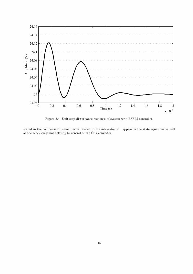
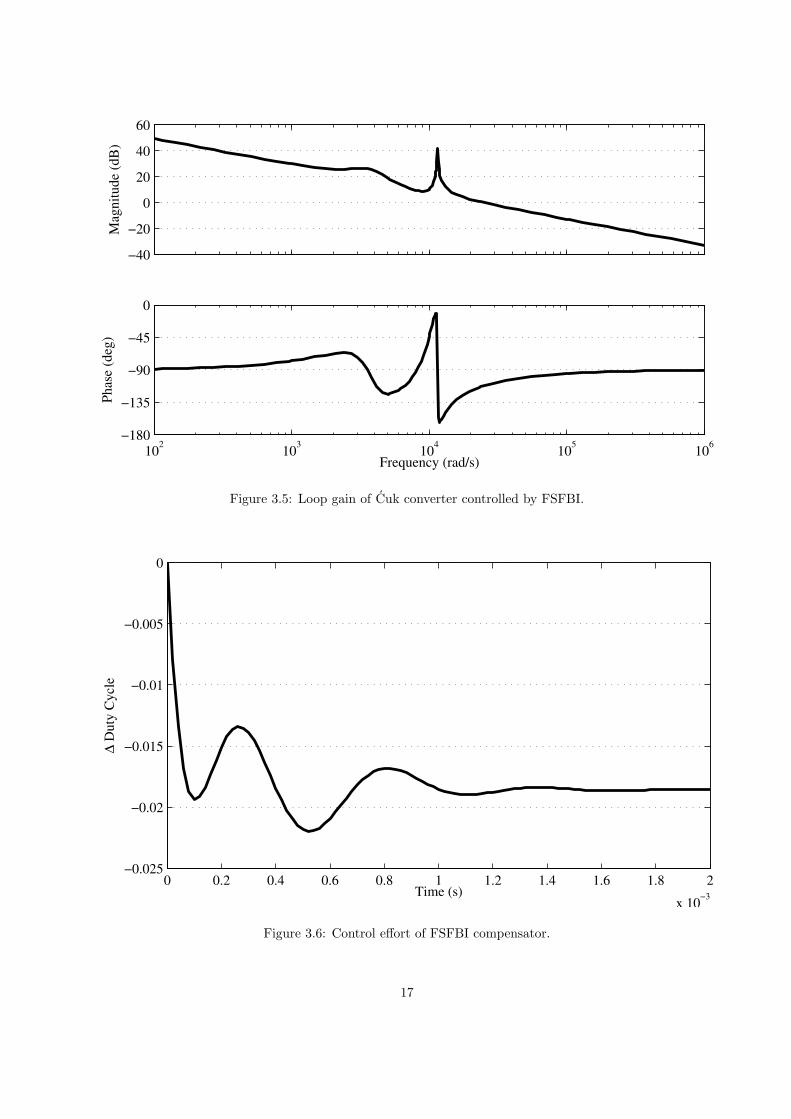
transient is shown in Figure 3.4. The loop gain of the controlled system may be seen in Figure 3.5, wherethe loop is broken at the large X shown on the control input d in Figure 3.2. MATLAB calculations givethe gain margin as ∞ and a phase margin of 68. Figure 3.6 shows the change in duty cycle effected by theFSFBI controller to control the Cuk converter. Note that the final value of the control effort is -0.018. Thisis the approximate change in duty cycle that is necessary to completely reject the unit step distubance in vgas shown in Figure 1.7.
From this point forward in this paper, all of the example compensator designs will include an integratorterm to completely reject the effects of the step disturbance in vg, and though sometimes not explicitly
15
0 0.2 0.4 0.6 0.8 1 1.2 1.4 1.6 1.8 2
x 10−3
23.98
24
24.02
24.04
24.06
24.08
24.1
24.12
24.14
24.16
Time (s)
Am
plitu
de (V
)
Figure 3.4: Unit step disturbance response of system with FSFBI controller.
stated in the compensator name, terms related to the integrator will appear in the state equations as wellas the block diagrams relating to control of the Cuk converter.
16
−40
−20
0
20
40
60M
agni
tude
(dB
)
102 103 104 105 106−180
−135
−90
−45
0
Phas
e (d
eg)
Frequency (rad/s)
Figure 3.5: Loop gain of Cuk converter controlled by FSFBI.
0 0.2 0.4 0.6 0.8 1 1.2 1.4 1.6 1.8 2
x 10−3
−0.025
−0.02
−0.015
−0.01
−0.005
0
Time (s)
∆ D
uty
Cyc
le
Figure 3.6: Control effort of FSFBI compensator.
17
Chapter 4
State Estimation
Since an n-th order system requires n states be fed back to the gain matrix K to allow pole placementanywhere in the complex plane, this requires at least n measurements of the state variables. This can beprohibitively expensive or complex. In some cases, the internal system states may not even be measurable.In general, only the input and output of a system are available to the control system designer. However, if thesystem is fully observable, a state estimator (also known as an observer) may be used to provide estimatedstates for use in feedback control. The use of an observer requires that the state estimates converge to theactual state values (if starting from different initial states) more rapidly than the system itself responds.The control law used is then:
u = −Kx (4.1)
where x indicates that the states fed back into the system are estimates.In order to quickly force the state estimate to converge to the actual values of the state from arbitrary
initial conditions, a correction term must be applied to the estimator dynamics such that the error dynamicsapproach zero rapidly.
4.1 Full-order State Estimators
System modeling from physical principles essentially produces a state estimator once it as been per-formed. Since the objective of modeling is to produce a mathematical representation of the system, and thatrepresentation is based on the dynamics predicted by physical principles, the resulting model is an estimator.
Assuming the system is observable, the output of the estimator Cx can be compared to the output ofthe system, and any difference between them may be multiplied by a gain vector and added to the stateestimator dynamics. Therefore:
e = y − Cx (4.2)
= C(x− x)
Multiplying this error by a gain vector L, the desired state error correction term is formed, which can thenbe added to the dynamics of the estimator to form:
˙x = Ax+Bu− LC(x− x) (4.3)
= (A− LC)x+Bu+ LCx
When L is chosen such that the eigenvalues of A−LC lie in the left half of the complex plane, the estimatorerror e → 0 as t → ∞. Since the state estimate must converge to the controlled state faster than the stateitself can change, the eigenvalues of A − LC should be placed farther to the left than the eigenvalues ofA − BK. A good rule of thumb is to make the estimator dynamics at least twice as fast as the controlledsystem dynamics.
18
The separation principle allows the control law gain K and the observer gain L to be determined in-dependently. The proof of this is in many other references (e.g., [2]), so it shall not be repeated here, butapplication shall be made of the principle in the design examples to follow.
When paired with the linear state feedback control law, the estimator-based compensator is formed. Forthe case of state feedback without an integral state added, the compensator is given by:
˙x = (A−BK − LC)x+ Ly (4.4)
u = −Kx
Where the state of the system has been augmented by an integrator state, the compensator is given by:
[
˙xxi
]
=
[
A−Bk − LC −Bki0 0
] [
x
xi
]
+
[
L
−1
]
y (4.5)
u =[
−k −ki]
[
x
xi
]
4.2 Full-Order Estimator-Based Compensator
The block diagram for the Cuk converter controlled with a full-order state estimator with linear controllaw and integral action is shown in Figure 4.1, and was used to derive the following closed-loop stateequations:
x = Ax−Bdkx−Bdkixi +Bvg (4.6)
xi = −Cx˙x = LCx−Bdkixi + (A−Bdk − LC) x
vo = Cx
and the associated state space matrices:
A =
A −Bdki −Bdk
−C 0 0LC −Bdki A−Bdk − LC
(4.7)
B =[
B 0 0]
′
C =[
C 0 0]
D = [D]
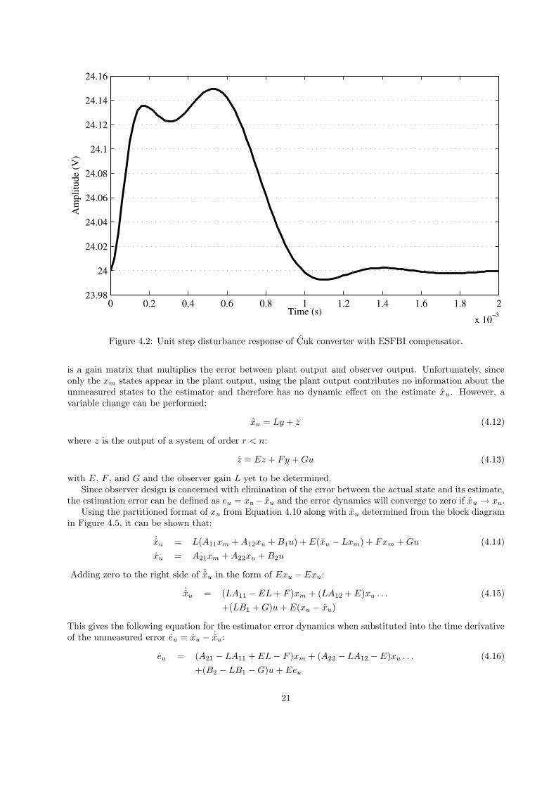
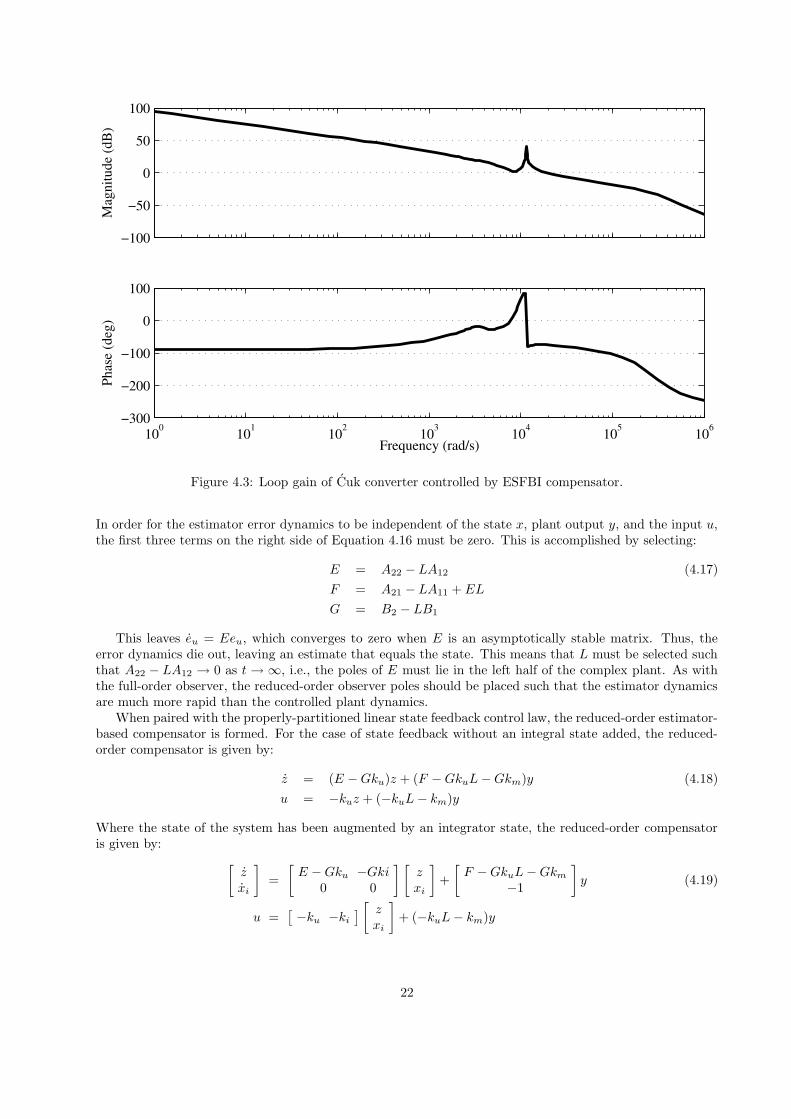
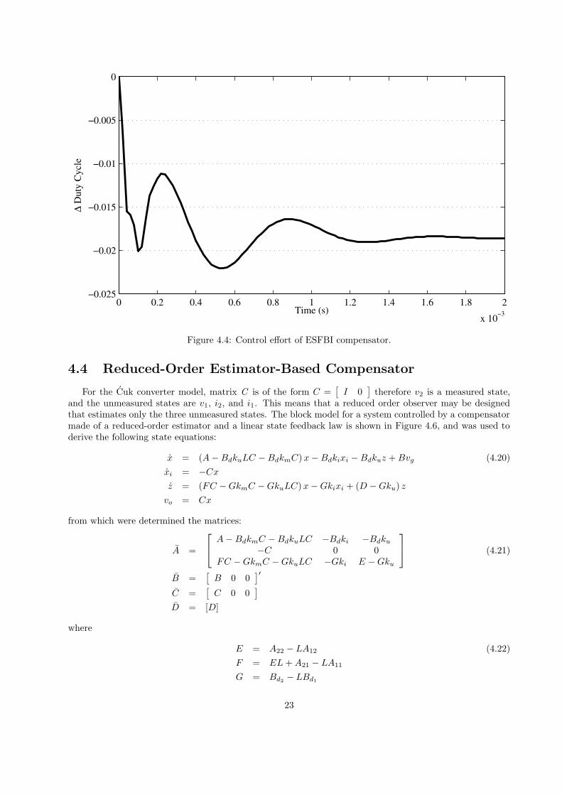
The step disturbance transient is shown in Figure 4.2. There is more oscillatory behavior in the initial partof the transient response compared to the response under FSFBI control. This is likely to be caused by theinitial estimation of states and their convergence to the actual state values. Comparison of the settling timesshows that they are approximately the same, and the only transient differences occur early in the transient.The loop gain of the controlled system may be seen in Figure 4.3, where the loop is broken at the large Xshown on the control input d in Figure 4.1. MATLAB calculations give the gain margin as 33.6 dB and aphase margin of 105. Figure 4.4 shows the control effort of the ESFBI controller.
Since the Cuk converter has only four states, the observer itself will be a fourth order system. Alongwith the integral state, the compensator becomes a fifth order system. When evaluating desired observerpole locations, keep in mind that the poles of the observer must be placed to the left of the poles of the plantby a large margin to ensure that the state estimator dynamics are faster than those of the plant.
4.3 Reduced-order State Estimators
If some of the states appear directly in the output as a function of the measurement equation (i.e., arenot a linear combination of other states), those states do not need to be estimated. Hence, a reduced-orderestimator may be constructed that only estimates those unmeasured states.
19
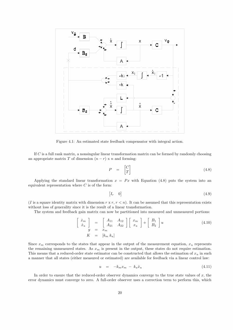
Figure 4.1: An estimated state feedback compensator with integral action.
If C is a full rank matrix, a nonsingular linear transformation matrix can be formed by randomly choosingan appropriate matrix T of dimension (n− r) x n and forming:
P =
[
C
T
]
(4.8)
Applying the standard linear transformation x = Px with Equation (4.8) puts the system into anequivalent representation where C is of the form:
[
Ir 0]
(4.9)
(I is a square identity matrix with dimension r x r, r < n). It can be assumed that this representation existswithout loss of generality since it is the result of a linear transformation.
The system and feedback gain matrix can now be partitioned into measured and unmeasured portions:
[
xmxu
]
=
[
A11 A12A21 A22
] [
xmxu
]
+
[
B1B2
]
u (4.10)
y = xm
K = [km ku]
Since xm corresponds to the states that appear in the output of the measurement equation, xu representsthe remaining unmeasured states. As xm is present in the output, these states do not require estimation.This means that a reduced-order state estimator can be constructed that allows the estimation of xu in sucha manner that all states (either measured or estimated) are available for feedback via a linear control law:
u = −kmxm − kuxu (4.11)
In order to ensure that the reduced-order observer dynamics converge to the true state values of x, theerror dynamics must converge to zero. A full-order observer uses a correction term to perform this, which
20
0 0.2 0.4 0.6 0.8 1 1.2 1.4 1.6 1.8 2
x 10−3
23.98
24
24.02
24.04
24.06
24.08
24.1
24.12
24.14
24.16
Time (s)
Am
plitu
de (V
)
Figure 4.2: Unit step disturbance response of Cuk converter with ESFBI compensator.
is a gain matrix that multiplies the error between plant output and observer output. Unfortunately, sinceonly the xm states appear in the plant output, using the plant output contributes no information about theunmeasured states to the estimator and therefore has no dynamic effect on the estimate xu. However, avariable change can be performed:
xu = Ly + z (4.12)
where z is the output of a system of order r < n:
z = Ez + Fy +Gu (4.13)
with E, F , and G and the observer gain L yet to be determined.Since observer design is concerned with elimination of the error between the actual state and its estimate,
the estimation error can be defined as eu = xu− xu and the error dynamics will converge to zero if xu → xu.Using the partitioned format of xu from Equation 4.10 along with xu determined from the block diagram
in Figure 4.5, it can be shown that:
˙xu = L(A11xm +A12xu +B1u) + E(xu − Lxm) + Fxm +Gu (4.14)
xu = A21xm +A22xu +B2u
Adding zero to the right side of ˙xu in the form of Exu −Exu:
˙xu = (LA11 − EL+ F )xm + (LA12 + E)xu . . . (4.15)
+(LB1 +G)u+ E(xu − xu)
This gives the following equation for the estimator error dynamics when substituted into the time derivativeof the unmeasured error eu = xu − ˙xu:
eu = (A21 − LA11 + EL− F )xm + (A22 − LA12 − E)xu . . . (4.16)
+(B2 − LB1 −G)u+ Eeu
21
−100
−50
0
50
100M
agni
tude
(dB
)
100 101 102 103 104 105 106−300
−200
−100
0
100
Phas
e (d
eg)
Frequency (rad/s)
Figure 4.3: Loop gain of Cuk converter controlled by ESFBI compensator.
In order for the estimator error dynamics to be independent of the state x, plant output y, and the input u,the first three terms on the right side of Equation 4.16 must be zero. This is accomplished by selecting:
E = A22 − LA12 (4.17)
F = A21 − LA11 + EL
G = B2 − LB1
This leaves eu = Eeu, which converges to zero when E is an asymptotically stable matrix. Thus, theerror dynamics die out, leaving an estimate that equals the state. This means that L must be selected suchthat A22 − LA12 → 0 as t → ∞, i.e., the poles of E must lie in the left half of the complex plant. As withthe full-order observer, the reduced-order observer poles should be placed such that the estimator dynamicsare much more rapid than the controlled plant dynamics.
When paired with the properly-partitioned linear state feedback control law, the reduced-order estimator-based compensator is formed. For the case of state feedback without an integral state added, the reduced-order compensator is given by:
z = (E −Gku)z + (F −GkuL−Gkm)y (4.18)
u = −kuz + (−kuL− km)y
Where the state of the system has been augmented by an integrator state, the reduced-order compensatoris given by:
[
z
xi
]
=
[
E −Gku −Gki0 0
] [
z
xi
]
+
[
F −GkuL−Gkm−1
]
y (4.19)
u =[
−ku −ki]
[
z
xi
]
+ (−kuL− km)y
22
0 0.2 0.4 0.6 0.8 1 1.2 1.4 1.6 1.8 2
x 10−3
−0.025
−0.02
−0.015
−0.01
−0.005
0
Time (s)
∆ D
uty
Cyc
le
Figure 4.4: Control effort of ESFBI compensator.
4.4 Reduced-Order Estimator-Based Compensator
For the Cuk converter model, matrix C is of the form C =[
I 0]
therefore v2 is a measured state,and the unmeasured states are v1, i2, and i1. This means that a reduced order observer may be designedthat estimates only the three unmeasured states. The block model for a system controlled by a compensatormade of a reduced-order estimator and a linear state feedback law is shown in Figure 4.6, and was used toderive the following state equations:
x = (A−BdkuLC −BdkmC)x−Bdkixi −Bdkuz +Bvg (4.20)
xi = −Cx
z = (FC −GkmC −GkuLC)x−Gkixi + (D −Gku) z
vo = Cx
from which were determined the matrices:
A =
A−BdkmC −BdkuLC −Bdki −Bdku−C 0 0
FC −GkmC −GkuLC −Gki E −Gku
(4.21)
B =[
B 0 0]
′
C =[
C 0 0]
D = [D]
where
E = A22 − LA12 (4.22)
F = EL+A21 − LA11
G = Bd2− LBd1
23
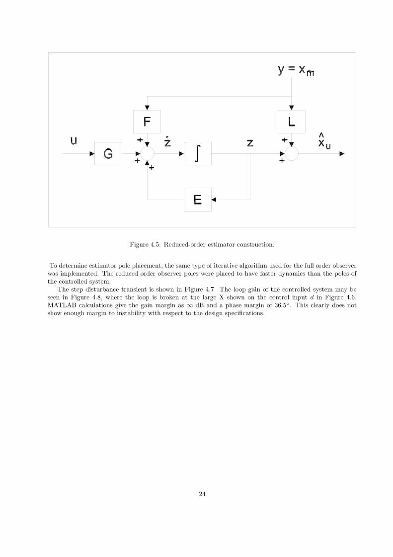
Figure 4.5: Reduced-order estimator construction.
To determine estimator pole placement, the same type of iterative algorithm used for the full order observerwas implemented. The reduced order observer poles were placed to have faster dynamics than the poles ofthe controlled system.
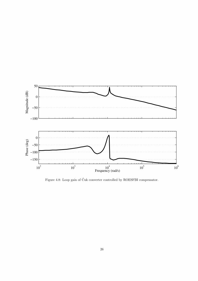
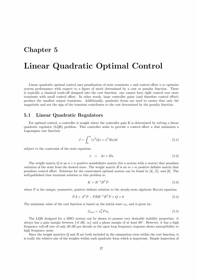
The step disturbance transient is shown in Figure 4.7. The loop gain of the controlled system may beseen in Figure 4.8, where the loop is broken at the large X shown on the control input d in Figure 4.6.MATLAB calculations give the gain margin as ∞ dB and a phase margin of 36.5. This clearly does notshow enough margin to instability with respect to the design specifications.
24
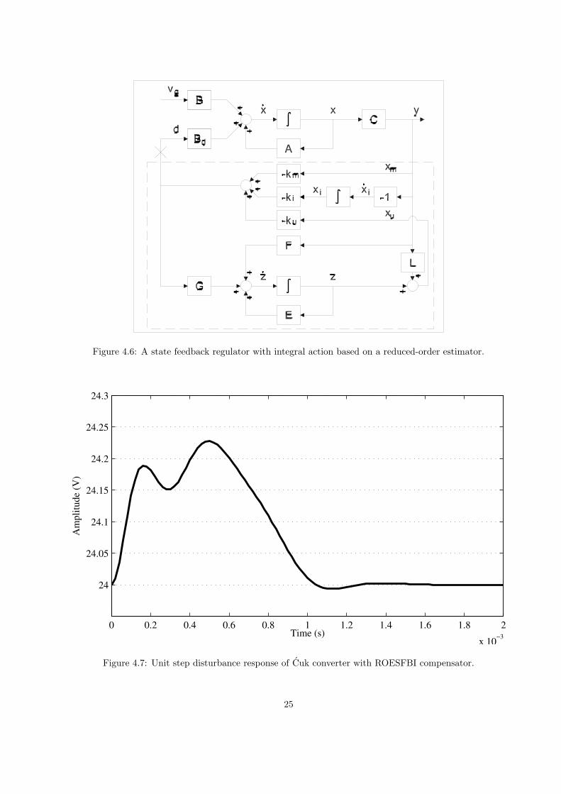
Figure 4.6: A state feedback regulator with integral action based on a reduced-order estimator.
0 0.2 0.4 0.6 0.8 1 1.2 1.4 1.6 1.8 2
x 10−3
24
24.05
24.1
24.15
24.2
24.25
24.3
Time (s)
Am
plitu
de (V
)
Figure 4.7: Unit step disturbance response of Cuk converter with ROESFBI compensator.
25
−100
−50
0
50
Mag
nitu
de (d
B)
102 103 104 105 106
−150
−100
−50
0
Phas
e (d
eg)
Frequency (rad/s)
Figure 4.8: Loop gain of Cuk converter controlled by ROESFBI compensator.
26
Chapter 5
Linear Quadratic Optimal Control
Linear quadratic optimal control uses penalization of state transients x and control effort u to optimizesystem performance with respect to a figure of merit determined by a cost or penalty function. Thereis typically a classical trade-off designed into the cost function: one cannot have tight control over statetransients with small control effort. In other words, large controller gains (and therefore control effort)produce the smallest output transients. Additionally, quadratic forms are used to ensure that only themagnitude and not the sign of the transient contributes to the cost determined by the penalty function.
5.1 Linear Quadratic Regulators
For optimal control, a controller is sought where the controller gain K is determined by solving a linearquadratic regulator (LQR) problem. This controller seeks to provide a control effort u that minimizes aLagrangian cost function:
J =
∫
∞
0
(xTQx+ uTRu)dt (5.1)
subject to the constraint of the state equation:
x = Ax+Bu (5.2)
The weight matrix Q is an n× n positive semidefinite matrix (for a system with n states) that penalizesvariation of the state from the desired state. The weight matrix R is an m×m positive definite matrix thatpenalizes control effort. Solutions for the constrained optimal system can be found in [4], [5], and [6]. Thewell-published time invariant solution to this problem is:
K = R−1BTP (5.3)
where P is the unique, symmetric, positive definite solution to the steady-state algebraic Riccati equation:
PA+ATP − PBR−1BTP +Q = 0 (5.4)
The minimum value of the cost function is based on the initial state x0, and is given by:
Jmin = xT0 Px0 (5.5)
The LQR designed for a SISO system can be shown to possess very desirable stability properties: italways has a gain margin between -6 dB, ∞ and a phase margin of at least 60. However, it has a highfrequency roll-off rate of only 20 dB per decade so the open loop frequency response shows susceptibility tohigh frequency noise.
Since the weight matrices Q and R are both included in the summation term within the cost function, itis really the relative size of the weights within each quadratic form which is important. Simple inspection of
27
the cost function shows that multiplying both weight matrices by the same real constant (e.g., κ) will notaffect their ratio. The multiplier κ may be factored out of the integral, thus returning the cost function to itsoriginal form. Thus, the problem of minimizing κJ becomes the same as minimizing J . Therefore, holdingone weight matrix constant while varying either the individual elements or a scalar multiplier of the otheris an acceptable technique for iterative design. It is good for the designer to maintain an understandingof the effects of manipulating individual weights, however. In general, raising the effective penalty a singlestate or control input by manipulating its individual weight will tighten the control over the variation inthat parameter, however it may do so at the expense of larger variation in the other states or inputs.
5.2 Cuk Converter with LQR Compensator
The fifth-order system formed by augmenting the Cuk converter with an integral state requires that Q bea five-by-five matrix. To review, the state vector is [v2 v1 i2 i1 xi]
′
, where xi corresponds to the integral of thereference error e. Since the states have physical significance in this model, it is easy to see that each voltage,current, or error transient may be individually penalized using the diagonal elements of the Q matrix. As theobjective of controlling the Cuk converter is to regulate the output vo = v2 in the face of disturbances to vg,penalizing transients that occur on state v2 is a logical choice, as is penalizing the state xi associated withthe reference error integral as the integral of that error should be minimized to provide for good regulation.Hence, the Q matrix chosen for design of the LQR has two positive entries corresponding to the first (Q11)and last (Q55) entries along the diagonal to ensure it is positive semidefinite. The Cuk converter has only asingle control input, and for initial design R was set equal to 1 arbitrarily. If the control effort exceeds thelimitations put on it (refer to Section 1.5), the value of R may need to be increase to penalize the controleffort.
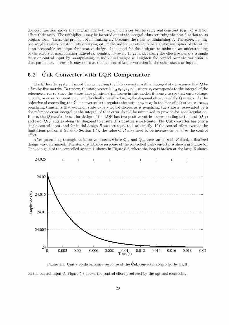
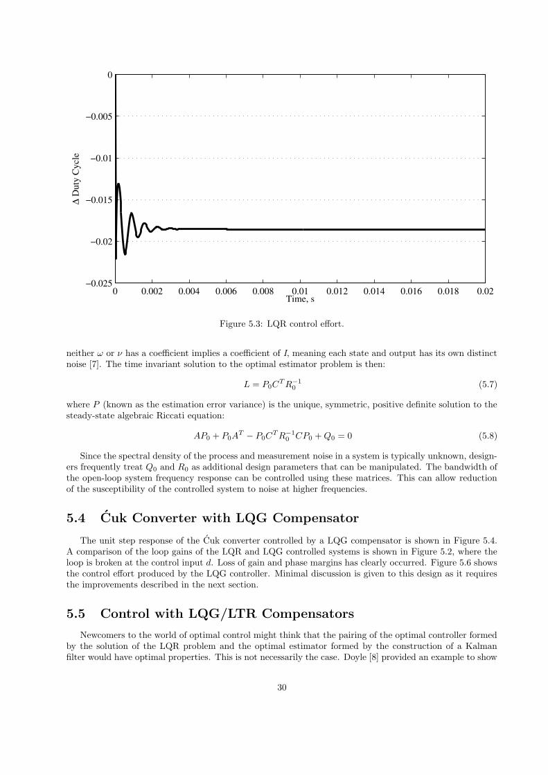
After proceeding through an iterative process where Q11 and Q55 were varied with R fixed, a finalizeddesign was determined. The step disturbance response of the controlled Cuk converter is shown in Figure 5.1The loop gain of the controlled system is shown in Figure 5.2, where the loop is broken at the large X shown
0 0.002 0.004 0.006 0.008 0.01 0.012 0.014 0.016 0.018 0.0224
24.005
24.01
24.015
24.02
24.025
Time (s)
Am
plitu
de (V
)
Figure 5.1: Unit step disturbance response of the Cuk converter controlled by LQR.
on the control input d. Figure 5.3 shows the control effort produced by the optimal controller.
28
−50
0
50
100M
agni
tude
(dB
)
101 102 103 104 105 106−200
−150
−100
−50
0
Phas
e (d
eg)
Frequency (rad/s)
Figure 5.2: Loop gain of Cuk converter controlled by LQR compensator.
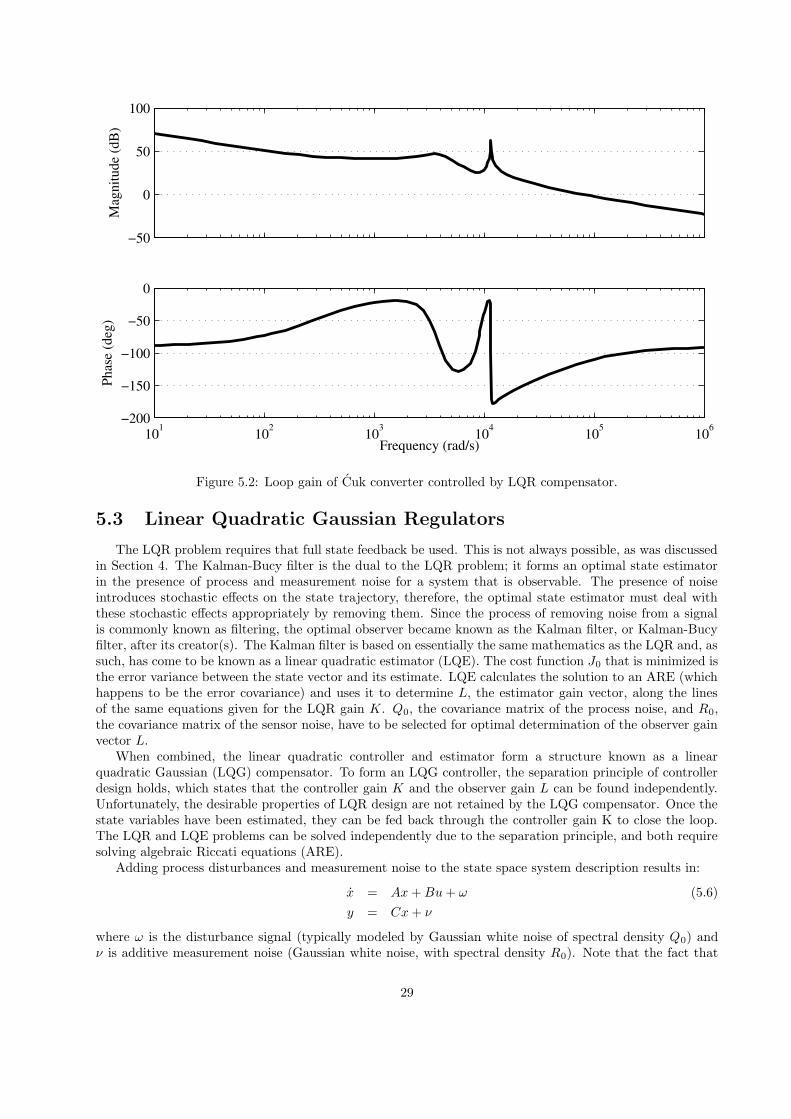
5.3 Linear Quadratic Gaussian Regulators
The LQR problem requires that full state feedback be used. This is not always possible, as was discussedin Section 4. The Kalman-Bucy filter is the dual to the LQR problem; it forms an optimal state estimatorin the presence of process and measurement noise for a system that is observable. The presence of noiseintroduces stochastic effects on the state trajectory, therefore, the optimal state estimator must deal withthese stochastic effects appropriately by removing them. Since the process of removing noise from a signalis commonly known as filtering, the optimal observer became known as the Kalman filter, or Kalman-Bucyfilter, after its creator(s). The Kalman filter is based on essentially the same mathematics as the LQR and, assuch, has come to be known as a linear quadratic estimator (LQE). The cost function J0 that is minimized isthe error variance between the state vector and its estimate. LQE calculates the solution to an ARE (whichhappens to be the error covariance) and uses it to determine L, the estimator gain vector, along the linesof the same equations given for the LQR gain K. Q0, the covariance matrix of the process noise, and R0,the covariance matrix of the sensor noise, have to be selected for optimal determination of the observer gainvector L.
When combined, the linear quadratic controller and estimator form a structure known as a linearquadratic Gaussian (LQG) compensator. To form an LQG controller, the separation principle of controllerdesign holds, which states that the controller gain K and the observer gain L can be found independently.Unfortunately, the desirable properties of LQR design are not retained by the LQG compensator. Once thestate variables have been estimated, they can be fed back through the controller gain K to close the loop.The LQR and LQE problems can be solved independently due to the separation principle, and both requiresolving algebraic Riccati equations (ARE).
Adding process disturbances and measurement noise to the state space system description results in:
x = Ax+Bu+ ω (5.6)
y = Cx+ ν
where ω is the disturbance signal (typically modeled by Gaussian white noise of spectral density Q0) andν is additive measurement noise (Gaussian white noise, with spectral density R0). Note that the fact that
29
0 0.002 0.004 0.006 0.008 0.01 0.012 0.014 0.016 0.018 0.02−0.025
−0.02
−0.015
−0.01
−0.005
0
Time, s
∆ D
uty
Cyc
le
Figure 5.3: LQR control effort.
neither ω or ν has a coefficient implies a coefficient of I, meaning each state and output has its own distinctnoise [7]. The time invariant solution to the optimal estimator problem is then:
L = P0CTR−1
0 (5.7)
where P (known as the estimation error variance) is the unique, symmetric, positive definite solution to thesteady-state algebraic Riccati equation:
AP0 + P0AT − P0C
TR−10 CP0 +Q0 = 0 (5.8)
Since the spectral density of the process and measurement noise in a system is typically unknown, design-ers frequently treat Q0 and R0 as additional design parameters that can be manipulated. The bandwidth ofthe open-loop system frequency response can be controlled using these matrices. This can allow reductionof the susceptibility of the controlled system to noise at higher frequencies.
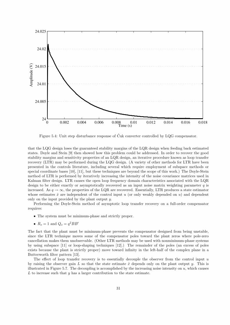
5.4 Cuk Converter with LQG Compensator
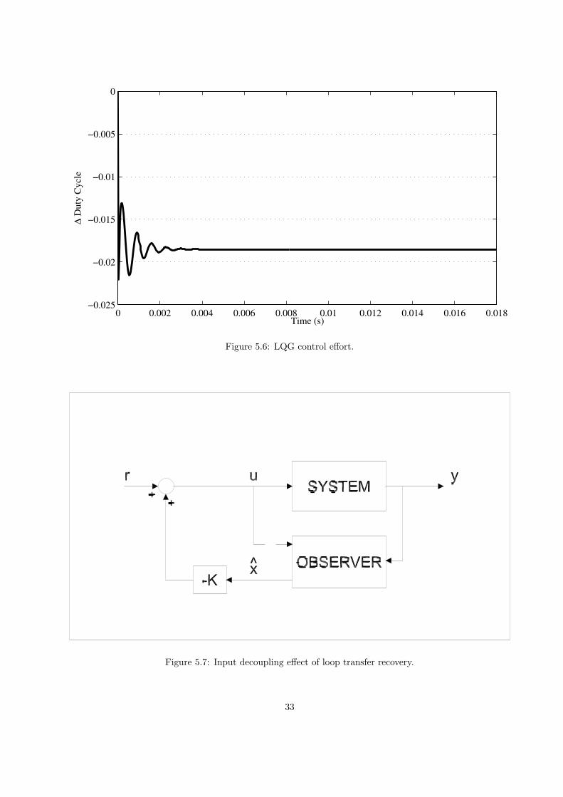
The unit step response of the Cuk converter controlled by a LQG compensator is shown in Figure 5.4.A comparison of the loop gains of the LQR and LQG controlled systems is shown in Figure 5.2, where theloop is broken at the control input d. Loss of gain and phase margins has clearly occurred. Figure 5.6 showsthe control effort produced by the LQG controller. Minimal discussion is given to this design as it requiresthe improvements described in the next section.
5.5 Control with LQG/LTR Compensators
Newcomers to the world of optimal control might think that the pairing of the optimal controller formedby the solution of the LQR problem and the optimal estimator formed by the construction of a Kalmanfilter would have optimal properties. This is not necessarily the case. Doyle [8] provided an example to show
30
0 0.002 0.004 0.006 0.008 0.01 0.012 0.014 0.016 0.01824
24.005
24.01
24.015
24.02
24.025
Time (s)
Am
plitu
de (V
)
Figure 5.4: Unit step disturbance response of Cuk converter controlled by LQG compensator.
that the LQG design loses the guaranteed stability margins of the LQR design when feeding back estimatedstates. Doyle and Stein [9] then showed how this problem could be addressed. In order to recover the goodstability margins and sensitivity properties of an LQR design, an iterative procedure known as loop transferrecovery (LTR) may be performed during the LQG design. (A variety of other methods for LTR have beenpresented in the controls literature, including several which require employment of subspace methods orspecial coordinate bases [10], [11], but these techniques are beyond the scope of this work.) The Doyle-Steinmethod of LTR is performed by iteratively increasing the intensity of the noise covariance matrices used inKalman filter design. LTR causes the open loop frequency domain characteristics associated with the LQRdesign to be either exactly or asymptotically recovered as an input noise matrix weighting parameter q isincreased. As q →∞, the properties of the LQR are recovered. Essentially, LTR produces a state estimatorwhose estimates x are independent of the control input u (or only weakly depended on u) and dependentonly on the input provided by the plant output y.
Performing the Doyle-Stein method of asymptotic loop transfer recovery on a full-order compensatorrequires:
• The system must be minimum-phase and strictly proper.
• Ro = 1 and Qo = q2BB′
The fact that the plant must be minimum-phase prevents the compensator designed from being unstable,since the LTR technique moves some of the compensator poles toward the plant zeros where pole-zerocancellation makes them unobservable. (Other LTR methods may be used with nonminimum-phase systemsby using subspace [11] or loop-shaping techniques [12].) The remainder of the poles (an excess of polesexists because the plant is strictly proper) move toward infinity in the left-half of the complex plane in aButterworth filter pattern [13].
The effect of loop transfer recovery is to essentially decouple the observer from the control input u
by raising the observer gain L so that the state estimate x depends only on the plant output y. This isillustrated in Figure 5.7. The decoupling is accomplished by the increasing noise intensity on u, which causesL to increase such that y has a larger contribution to the state estimate.
31
−100
−50
0
50
100M
agni
tude
(dB
)
101 102 103 104 105 106−270
−180
−90
0
Phas
e (d
eg)
Frequency (rad/s)
LQRLQG
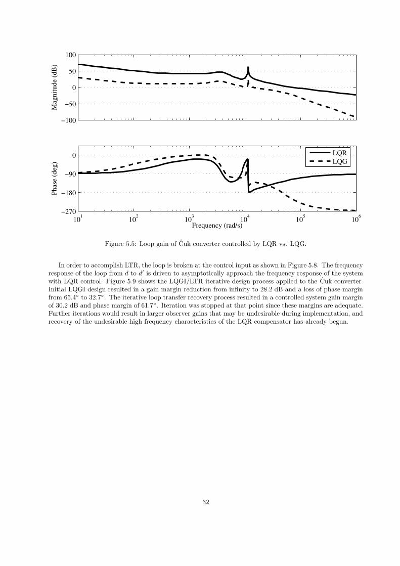
Figure 5.5: Loop gain of Cuk converter controlled by LQR vs. LQG.
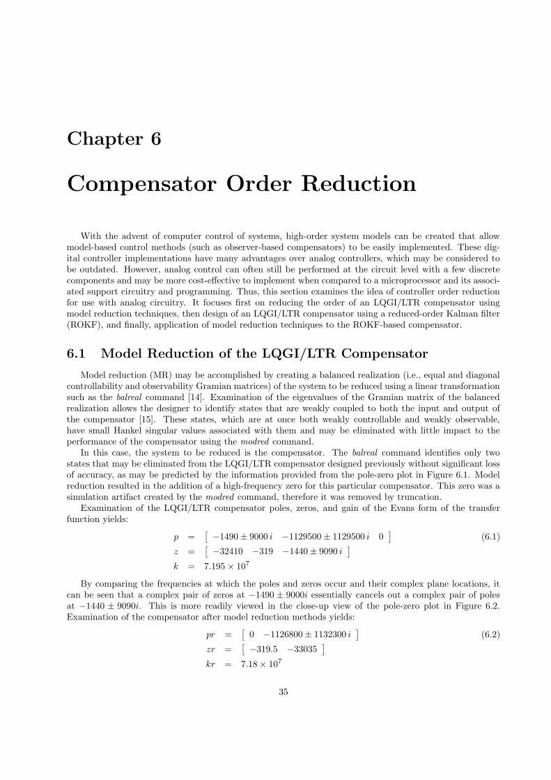
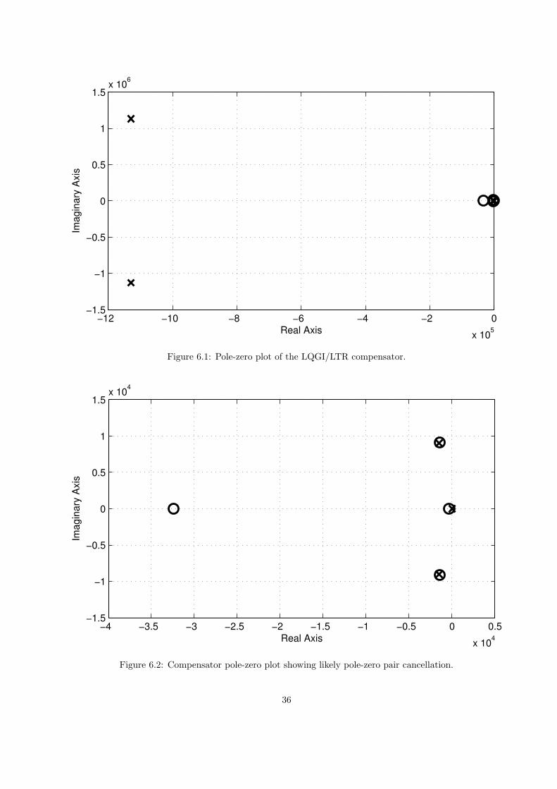
In order to accomplish LTR, the loop is broken at the control input as shown in Figure 5.8. The frequencyresponse of the loop from d to d′ is driven to asymptotically approach the frequency response of the systemwith LQR control. Figure 5.9 shows the LQGI/LTR iterative design process applied to the Cuk converter.Initial LQGI design resulted in a gain margin reduction from infinity to 28.2 dB and a loss of phase marginfrom 65.4 to 32.7. The iterative loop transfer recovery process resulted in a controlled system gain marginof 30.2 dB and phase margin of 61.7. Iteration was stopped at that point since these margins are adequate.Further iterations would result in larger observer gains that may be undesirable during implementation, andrecovery of the undesirable high frequency characteristics of the LQR compensator has already begun.
32
0 0.002 0.004 0.006 0.008 0.01 0.012 0.014 0.016 0.018−0.025
−0.02
−0.015
−0.01
−0.005
0
Time (s)
∆ D
uty
Cyc
le
Figure 5.6: LQG control effort.
Figure 5.7: Input decoupling effect of loop transfer recovery.
33
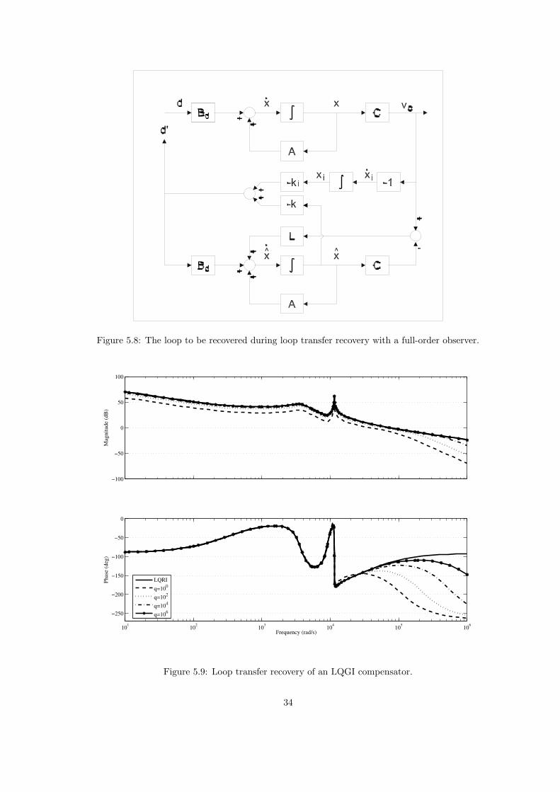
Figure 5.8: The loop to be recovered during loop transfer recovery with a full-order observer.
−100
−50
0
50
100
Mag
nitu
de (d
B)
101 102 103 104 105 106
−250
−200
−150
−100
−50
0
Phas
e (d
eg)
Frequency (rad/s)
LQRI
q=100
q=102
q=104
q=106
Figure 5.9: Loop transfer recovery of an LQGI compensator.
34
Chapter 6
Compensator Order Reduction
With the advent of computer control of systems, high-order system models can be created that allowmodel-based control methods (such as observer-based compensators) to be easily implemented. These dig-ital controller implementations have many advantages over analog controllers, which may be considered tobe outdated. However, analog control can often still be performed at the circuit level with a few discretecomponents and may be more cost-effective to implement when compared to a microprocessor and its associ-ated support circuitry and programming. Thus, this section examines the idea of controller order reductionfor use with analog circuitry. It focuses first on reducing the order of an LQGI/LTR compensator usingmodel reduction techniques, then design of an LQGI/LTR compensator using a reduced-order Kalman filter(ROKF), and finally, application of model reduction techniques to the ROKF-based compensator.
6.1 Model Reduction of the LQGI/LTR Compensator
Model reduction (MR) may be accomplished by creating a balanced realization (i.e., equal and diagonalcontrollability and observability Gramian matrices) of the system to be reduced using a linear transformationsuch as the balreal command [14]. Examination of the eigenvalues of the Gramian matrix of the balancedrealization allows the designer to identify states that are weakly coupled to both the input and output ofthe compensator [15]. These states, which are at once both weakly controllable and weakly observable,have small Hankel singular values associated with them and may be eliminated with little impact to theperformance of the compensator using the modred command.
In this case, the system to be reduced is the compensator. The balreal command identifies only twostates that may be eliminated from the LQGI/LTR compensator designed previously without significant lossof accuracy, as may be predicted by the information provided from the pole-zero plot in Figure 6.1. Modelreduction resulted in the addition of a high-frequency zero for this particular compensator. This zero was asimulation artifact created by the modred command, therefore it was removed by truncation.
Examination of the LQGI/LTR compensator poles, zeros, and gain of the Evans form of the transferfunction yields:
p =[
−1490± 9000 i −1129500± 1129500 i 0]
(6.1)
z =[
−32410 −319 −1440± 9090 i]
k = 7.195× 10⁷
By comparing the frequencies at which the poles and zeros occur and their complex plane locations, itcan be seen that a complex pair of zeros at −1490 ± 9000i essentially cancels out a complex pair of polesat −1440 ± 9090i. This is more readily viewed in the close-up view of the pole-zero plot in Figure 6.2.Examination of the compensator after model reduction methods yields:
pr =[
0 −1126800± 1132300 i]
(6.2)
zr =[
−319.5 −33035]
kr = 7.18× 10⁷
35
−12 −10 −8 −6 −4 −2 0
x 105
−1.5
−1
−0.5
0
0.5
1
1.5x 10⁶
Imag
inar
y A
xis
Real Axis
Figure 6.1: Pole-zero plot of the LQGI/LTR compensator.
−4 −3.5 −3 −2.5 −2 −1.5 −1 −0.5 0 0.5
x 104
−1.5
−1
−0.5
0
0.5
1
1.5x 10⁴
Imag
inar
y A
xis
Real Axis
Figure 6.2: Compensator pole-zero plot showing likely pole-zero pair cancellation.
36
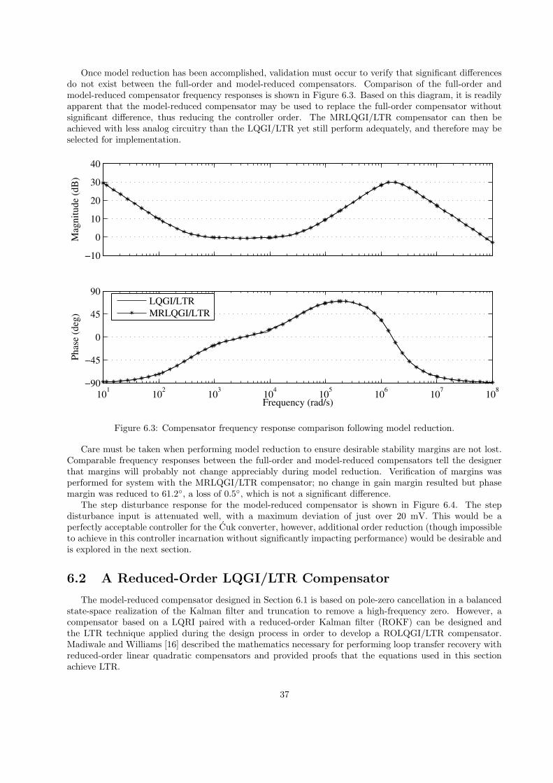
Once model reduction has been accomplished, validation must occur to verify that significant differencesdo not exist between the full-order and model-reduced compensators. Comparison of the full-order andmodel-reduced compensator frequency responses is shown in Figure 6.3. Based on this diagram, it is readilyapparent that the model-reduced compensator may be used to replace the full-order compensator withoutsignificant difference, thus reducing the controller order. The MRLQGI/LTR compensator can then beachieved with less analog circuitry than the LQGI/LTR yet still perform adequately, and therefore may beselected for implementation.
−10
0
10
20
30
40
Mag
nitu
de (d
B)
101 102 103 104 105 106 107 108−90
−45
0
45
90
Phas
e (d
eg)
Frequency (rad/s)
LQGI/LTRMRLQGI/LTR
Figure 6.3: Compensator frequency response comparison following model reduction.
Care must be taken when performing model reduction to ensure desirable stability margins are not lost.Comparable frequency responses between the full-order and model-reduced compensators tell the designerthat margins will probably not change appreciably during model reduction. Verification of margins wasperformed for system with the MRLQGI/LTR compensator; no change in gain margin resulted but phasemargin was reduced to 61.2, a loss of 0.5, which is not a significant difference.
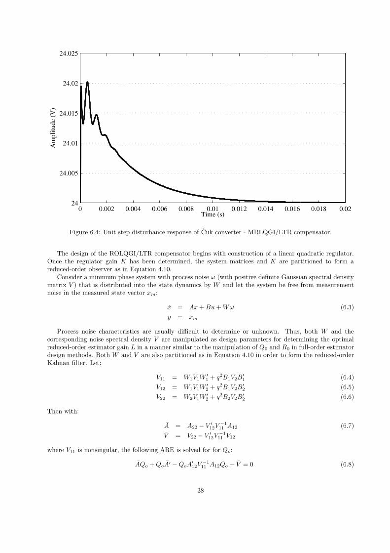
The step disturbance response for the model-reduced compensator is shown in Figure 6.4. The stepdisturbance input is attenuated well, with a maximum deviation of just over 20 mV. This would be aperfectly acceptable controller for the Cuk converter, however, additional order reduction (though impossibleto achieve in this controller incarnation without significantly impacting performance) would be desirable andis explored in the next section.
6.2 A Reduced-Order LQGI/LTR Compensator
The model-reduced compensator designed in Section 6.1 is based on pole-zero cancellation in a balancedstate-space realization of the Kalman filter and truncation to remove a high-frequency zero. However, acompensator based on a LQRI paired with a reduced-order Kalman filter (ROKF) can be designed andthe LTR technique applied during the design process in order to develop a ROLQGI/LTR compensator.Madiwale and Williams [16] described the mathematics necessary for performing loop transfer recovery withreduced-order linear quadratic compensators and provided proofs that the equations used in this sectionachieve LTR.
37
0 0.002 0.004 0.006 0.008 0.01 0.012 0.014 0.016 0.018 0.0224
24.005
24.01
24.015
24.02
24.025
Time (s)
Am
plitu
de (V
)
Figure 6.4: Unit step disturbance response of Cuk converter - MRLQGI/LTR compensator.
The design of the ROLQGI/LTR compensator begins with construction of a linear quadratic regulator.Once the regulator gain K has been determined, the system matrices and K are partitioned to form areduced-order observer as in Equation 4.10.
Consider a minimum phase system with process noise ω (with positive definite Gaussian spectral densitymatrix V ) that is distributed into the state dynamics by W and let the system be free from measurementnoise in the measured state vector xm:
x = Ax+Bu+Wω (6.3)
y = xm
Process noise characteristics are usually difficult to determine or unknown. Thus, both W and thecorresponding noise spectral density V are manipulated as design parameters for determining the optimalreduced-order estimator gain L in a manner similar to the manipulation of Q0 and R0 in full-order estimatordesign methods. Both W and V are also partitioned as in Equation 4.10 in order to form the reduced-orderKalman filter. Let:
V11 = W1V1W′
1 + q2B1V2B′
1 (6.4)
V12 = W1V1W′
2 + q2B1V2B′
2 (6.5)
V22 = W2V1W′
2 + q2B2V2B′
2 (6.6)
Then with:
A = A22 − V ′
12V−111 A12 (6.7)
V = V22 − V ′
12V−111 V12
where V11 is nonsingular, the following ARE is solved for for Qo:
AQo +QoA′ −QoA′
12V−111 A12Qo + V = 0 (6.8)
38
The Kalman filter gain L can then be determined from:
L = (QoA′
12 + V ′
12)V−111 (6.9)
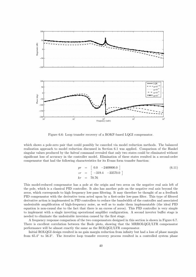
Now, as q is increased in Equations 6.4-6.6, the target feedback loop of the LQR controller is recovered.Once again the loop is broken at the control input as shown in Figure 6.5. The frequency response of
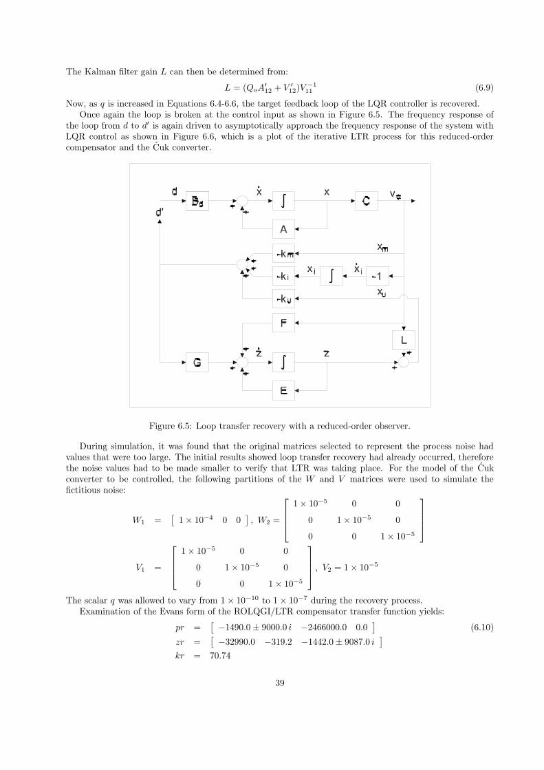
the loop from d to d′ is again driven to asymptotically approach the frequency response of the system withLQR control as shown in Figure 6.6, which is a plot of the iterative LTR process for this reduced-ordercompensator and the Cuk converter.
Figure 6.5: Loop transfer recovery with a reduced-order observer.
During simulation, it was found that the original matrices selected to represent the process noise hadvalues that were too large. The initial results showed loop transfer recovery had already occurred, thereforethe noise values had to be made smaller to verify that LTR was taking place. For the model of the Cukconverter to be controlled, the following partitions of the W and V matrices were used to simulate thefictitious noise:
W1 =[
1× 10⁻⁴ 0 0]
, W2 =
1× 10⁻⁵ 0 0
0 1× 10⁻⁵ 0
0 0 1× 10⁻⁵
V1 =
1× 10⁻⁵ 0 0
0 1× 10⁻⁵ 0
0 0 1× 10⁻⁵
, V2 = 1× 10⁻⁵
The scalar q was allowed to vary from 1× 10⁻¹⁰ to 1× 10⁻⁷ during the recovery process.Examination of the Evans form of the ROLQGI/LTR compensator transfer function yields:
pr =[
−1490.0± 9000.0 i −2466000.0 0.0]
(6.10)
zr =[
−32990.0 −319.2 −1442.0± 9087.0 i]
kr = 70.74
39
−100
−50
0
50
100
Mag
nitu
de (d
B)
102 103 104 105 106−200
−150
−100
−50
0
50
100
Phas
e (d
eg)
Frequency (rad/s)
LQR
q=10−10
q=10−9
q=10−8
q=10−7
Figure 6.6: Loop transfer recovery of a ROKF-based LQGI compensator.
which shows a pole-zero pair that could possibly be canceled via model reduction methods. The balancedrealization approach to model reduction discussed in Section 6.1 was applied. Comparison of the Hankelsingular values produced by the balreal command revealed that only two states could be eliminated withoutsignificant loss of accuracy in the controller model. Elimination of these states resulted in a second-ordercompensator that had the following characteristics for its Evans form transfer function:
pr =[
0.0 −2469000.0]
(6.11)
zr =[
−319.4 −33570.0]
kr = 70.76
This model-reduced compensator has a pole at the origin and two zeros on the negative real axis left ofthe pole, which is a classical PID controller. It also has another pole on the negative real axis beyond thezeros, which corresponds to high frequency low-pass filtering. It may therefore be thought of as a feedbackPID compensator with the derivative term acted upon by a first-order low-pass filter. This type of filteredderivative action is implemented in PID controllers to reduce the bandwidth of the controller and associatedundesirable amplification of high-frequency noise, as well as to make them implementable (the ideal PIDequation is non-causal due to the fact that there is an excess of zeros). This PID controller is very simpleto implement with a single inverting operational amplifier configuration. A second inverter buffer stage isneeded to eliminate the undesirable inversion caused by the first stage.
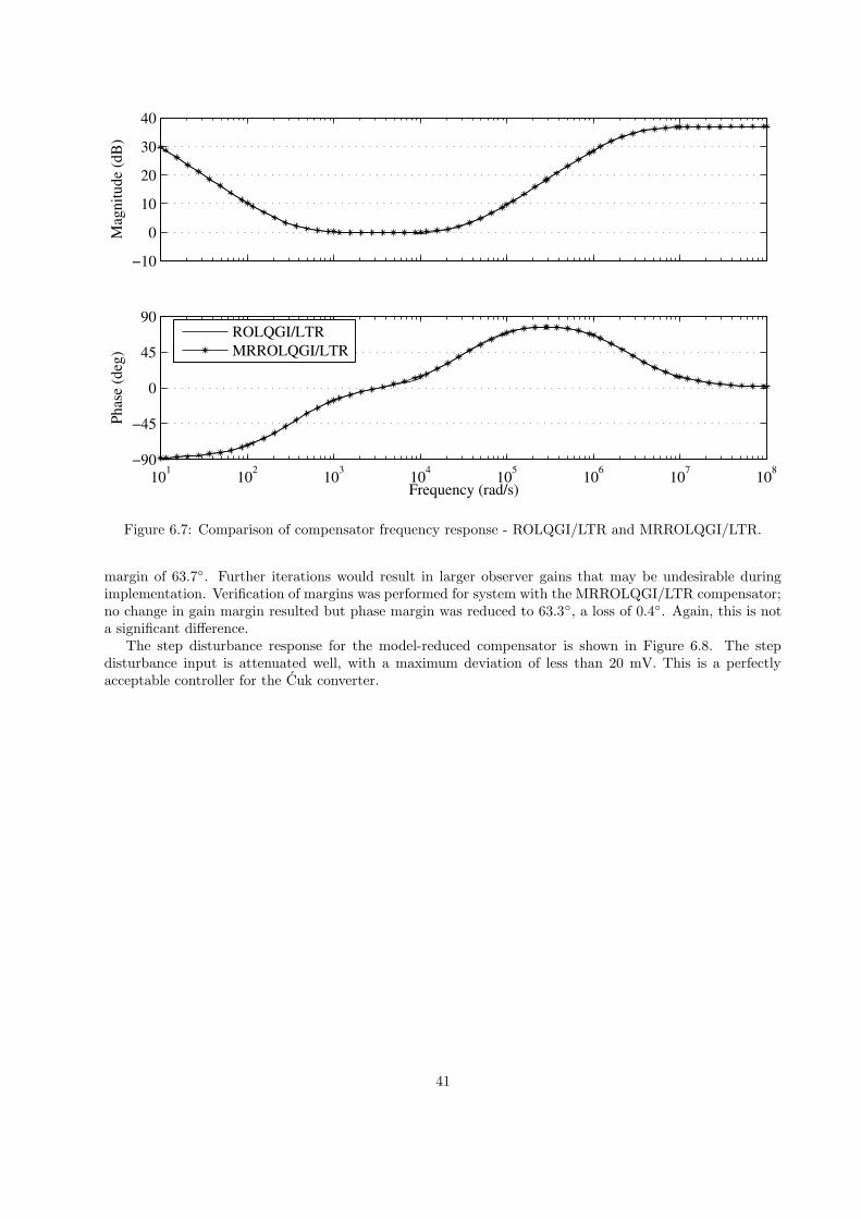
A frequency response comparison of the two compensators designed in this section is shown in Figure 6.7.There is excellent correlation between the Bode plots, showing that the MRROLQGI/LTR compensatorperformance will be almost exactly the same as the ROLQGI/LTR compensator.
Initial ROLQGI design resulted in no gain margin reduction from infinity but had a loss of phase marginfrom 65.4 to 56.3. The iterative loop transfer recovery process resulted in a controlled system phase
40
−10
0
10
20
30
40M
agni
tude
(dB
)
101 102 103 104 105 106 107 108−90
−45
0
45
90
Phas
e (d
eg)
Frequency (rad/s)
ROLQGI/LTRMRROLQGI/LTR
Figure 6.7: Comparison of compensator frequency response - ROLQGI/LTR and MRROLQGI/LTR.
margin of 63.7. Further iterations would result in larger observer gains that may be undesirable duringimplementation. Verification of margins was performed for system with the MRROLQGI/LTR compensator;no change in gain margin resulted but phase margin was reduced to 63.3, a loss of 0.4. Again, this is nota significant difference.
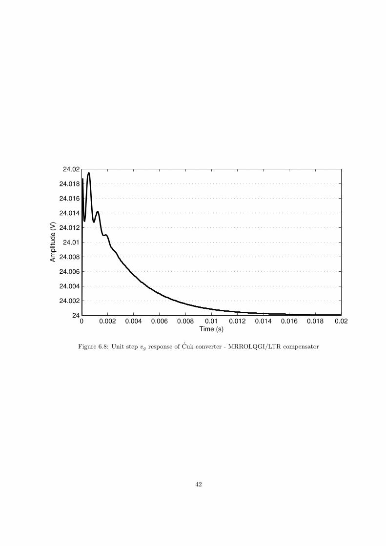
The step disturbance response for the model-reduced compensator is shown in Figure 6.8. The stepdisturbance input is attenuated well, with a maximum deviation of less than 20 mV. This is a perfectlyacceptable controller for the Cuk converter.
41
0 0.002 0.004 0.006 0.008 0.01 0.012 0.014 0.016 0.018 0.0224
24.002
24.004
24.006
24.008
24.01
24.012
24.014
24.016
24.018
24.02
Time (s)
Am
plitu
de (V
)
Figure 6.8: Unit step vg response of Cuk converter - MRROLQGI/LTR compensator
42
Chapter 7
Compensator Implementation
At this point, four optimal compensator designs that rely on output feedback and state estimation havebeen developed. The initial design of the optimal compensator began with a fifth-order controller comprisingfour estimated states for each of the states in the plant and an augmented integral state (LQGI/LTR).Model reduction techniques applied directly resulted in a third-order controller (MRLQGI/LTR), which wasa significant improvement in terms of minimizing the circuitry for implementation. The final design beganwith a fourth-order compensator based on a three states from a reduced-order observer augmented by anintegral state (ROLQGI/LTR), to which model reduction techniques were applied to form a second-ordertransfer function (MRROLQGI/LTR). This final regulator had the form of a classical PID controller. Thefinal design had a significant reduction in circuitry yet maintained excellent performance in both the timeand frequency domains.
The reduced-order compensators developed in Section 6 using model reduction techniques can be im-plemented with analog circuits using operational amplifiers. The goal is to use the minimum amount ofcomponents and circuitry for control (to minimize manufacturing costs) while maintaining adequate con-troller performance.
7.1 Model-Reduced LQG/LTR Compensator Implementation
The model-reduced compensator designed in Section 6.1 has two zeros on the negative real axis, aLHP pair of complex poles, and a pole at the origin. This compensator can be implemented by a PIcompensator cascaded with a Tow-Thomas biquadratic filter as seen in Figure 7.1. The Tow-Thomas filteris a general second-order filter able to implement low-pass, high-pass, band-pass, notch, and all-pass filterswith appropriate choices of coefficients of the filter transfer function [17]:
Tb(s) =a2s
2 + a1s+ a0
b2s2 + b1s+ b0(7.1)
The biquad filter section is used to implement the second-order denominator term with a simple zero bysetting a2 = 0. The PI section is used to implement the other real zero and the pole at the origin. For bothsections, it is desirable to keep the poles and zeros within a certain frequency tolerance of each other to keepthe component values reasonable in size. The transfer function of the PI section is given by:
Tp(s) = −C1
C2
(s+ 1C1R1
)
s(7.2)
The transfer function of the biquad filter section is given by:
Tb(s) = −
1C3R2
s+ 1C2
3R4R5
s2 + 1C3R3
s+ 1C2
3R2
4
(7.3)
43
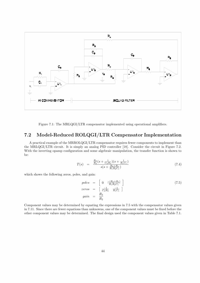
Figure 7.1: The MRLQGI/LTR compensator implemented using operational amplifiers.
7.2 Model-Reduced ROLQGI/LTR Compensator Implementation
A practical example of the MRROLQGI/LTR compensator requires fewer components to implement thanthe MRLQGI/LTR circuit. It is simply an analog PID controller [18]. Consider the circuit in Figure 7.2.With the inverting opamp configuration and some algebraic manipulation, the transfer function is shown tobe:
T (s) =R3
R2
(s+ 1C2R3
)(s+ 1R1C1
)
s(s+ R2+R1
R1R2C1
)(7.4)
which shows the following zeros, poles, and gain:
poles =[
0 −(R2+R1)R1R2C1
]
(7.5)
zeros =[
−1C2R3
−1R1C1
]
gain =R3
R2
Component values may be determined by equating the expressions in 7.5 with the compensator values givenin 7.11. Since there are fewer equations than unknowns, one of the component values must be fixed before theother component values may be determined. The final design used the component values given in Table 7.1.
44
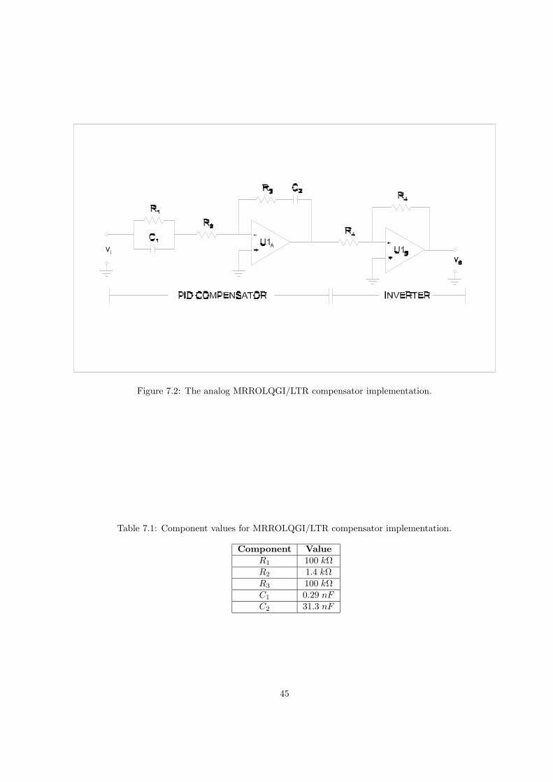
Figure 7.2: The analog MRROLQGI/LTR compensator implementation.
Table 7.1: Component values for MRROLQGI/LTR compensator implementation.
Component Value
R1 100 kΩR2 1.4 kΩR3 100 kΩC1 0.29 nFC2 31.3 nF
45
Chapter 8
Power Electronic Circuit Simulation
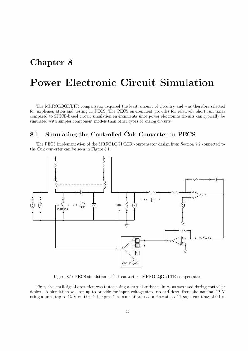
The MRROLQGI/LTR compensator required the least amount of circuitry and was therefore selectedfor implementation and testing in PECS. The PECS environment provides for relatively short run timescompared to SPICE-based circuit simulation environments since power electronics circuits can typically besimulated with simpler component models than other types of analog circuits.
8.1 Simulating the Controlled Cuk Converter in PECS
The PECS implementation of the MRROLQGI/LTR compensator design from Section 7.2 connected tothe Cuk converter can be seen in Figure 8.1.
Figure 8.1: PECS simulation of Cuk converter - MRROLQGI/LTR compensator.
First, the small-signal operation was tested using a step disturbance in vg as was used during controllerdesign. A simulation was set up to provide for input voltage steps up and down from the nominal 12 Vusing a unit step to 13 V on the Cuk input. The simulation used a time step of 1 µs, a run time of 0.1 s.
46
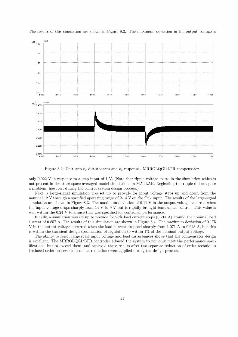
The results of this simulation are shown in Figure 8.2. The maximum deviation in the output voltage is
Figure 8.2: Unit step vg disturbances and vo response - MRROLQGI/LTR compensator.
only 0.022 V in response to a step input of 1 V. (Note that ripple voltage exists in the simulation which isnot present in the state space averaged model simulations in MATLAB. Neglecting the ripple did not posea problem, however, during the control system design process.)
Next, a large-signal simulation was set up to provide for input voltage steps up and down from thenominal 12 V through a specified operating range of 9-14 V on the Cuk input. The results of the large-signalsimulation are shown in Figure 8.3. The maximum deviation of 0.11 V in the output voltage occurred whenthe input voltage drops sharply from 14 V to 9 V but is rapidly brought back under control. This value iswell within the 0.24 V tolerance that was specified for controller performance.
Finally, a simulation was set up to provide for 25% load current steps (0.214 A) around the nominal loadcurrent of 0.857 A. The results of this simulation are shown in Figure 8.4. The maximum deviation of 0.175V in the output voltage occurred when the load current dropped sharply from 1.071 A to 0.643 A, but thisis within the transient design specification of regulation to within 1% of the nominal output voltage.
The ability to reject large scale input voltage and load disturbances shows that the compensator designis excellent. The MRROLQGI/LTR controller allowed the system to not only meet the performance spec-ifications, but to exceed them, and achieved these results after two separate reduction of order techniques(reduced-order observer and model reduction) were applied during the design process.
47
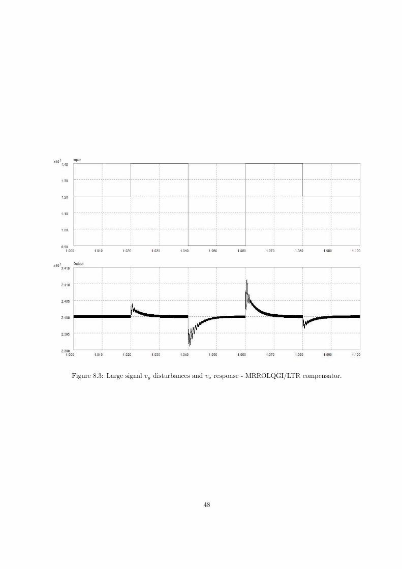
Figure 8.3: Large signal vg disturbances and vo response - MRROLQGI/LTR compensator.
48
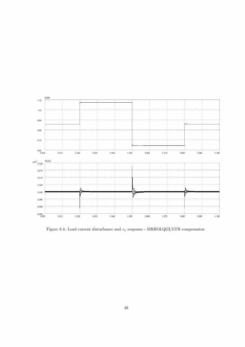
Figure 8.4: Load current disturbance and vo response - MRROLQGI/LTR compensator.
49

Chapter 9
Conclusion
This thesis showed the process of modern control design methods applied to regulator design for a CukDC-DC converter. Full state feedback control for pole placement was applied - first without integral effort,then with an integrator added. Output compensation using state estimation techniques with full- andreduced-order observers was then discussed and simulated. LQR and LQG/LTR techniques were then usedto design compensators that were optimized with respect to quadratic performance indices based on stateand control effort transients. Finally, two methods of model reduction were introduced. Balanced realizationof the LQGI/LTR compensator identified weakly controllable/observable states, which were then removedusing truncation to create a third-order compensator (MRLQGI/LTR) that could be implemented with acombination PI/Tow-Thomas biquad circuit. When the reduced-order Kalman filter-based compensatordesign (ROLQGI/LTR) was combined with model reduction using a balanced realization, the result was asecond-order compensator (MRROLQGI/LTR) implementable by an analog PID compensator. Since fewercomponents were necessary, the Cuk converter with MRROLQGI/LTR compensator was simulated in apower electronics modeling environment and showed excellent input voltage and load current disturbancerejection abilities.
50
Appendix A
The Cuk ConverterCircuit Model Derivations
A.1 Component Values
Cuk converter circuit component values used in this paper:
L1 = 0.5mH
R1 = 0.01Ω
L2 = 7.5mH
R2 = 0.01Ω
M = −1.5mH
C1 = 2.0µF
C2 = 20µF
R = 30Ω
Vg = 12V
d = 0.667
f = 100 kHz
A.2 Analysis of Inductors with Mutual Couplingand Equivalent Series Resistances
The equations for the voltage across two inductors L1 and L2 joined by mutual coupling are:
vL1= L1
di1
dt+M
di2
dt
vL2= M
di1
dt+ L2
di2
dt
The solutions of the two simultaneous equations are:
di1
dt=
L2
L1L2 −M2vL1
+−M
L1L2 −M2vL2
di2
dt=
−M
L1L2 −M2vL1
+L1
L1L2 −M2vL2
51

For the circuit with equivalent series resistances included in the inductor models when Q1 conducts:
vL1= vg − i1R1
vL2= v1 − v2 − i2R2
therefore:
di1
dt=
M
σ2v2 +
−M
σ2v1 +
MR2
σ2i2 +
−L2R1σ2
i1 +L2
σ2vg
di2
dt=
−L1σ2
v2 +L1
σ2v1 +
−L1R2σ2
i2 +MR1
σ2i1 +
−M
σ2vg
with σ2 = L1L2 −M2.
52

When Q1 does not conduct:
vL1= vg − i1R1 − v1
vL2= −v2 − i2R2
therefore:
di1
dt=
M
σ2v2 +
−L2σ2
v1 +MR2
σ2i2 +
−L2R1σ2
i1 +L2
σ2vg
di2
dt=
−L1σ2
v2 +M
σ2v1 +
−L1R2σ2
i2 +MR1
σ2i1 +
−M
σ2vg
with σ2 = L1L2 −M2.
A.3 The State Space Averaged Model
State space averaging is a well-known method used in modeling switching converters. For a system witha single switching component with a nominal duty cycle, a model may be developed by determining the stateand measurement equations for each of the two switch states, then calculating a weighted average of the twosets of equations using the nominal values of the time spent in each state as the weights. To develop thestate space averaged model, the equations for the rate of inductor current change derived in the precedingsection are used along with the equations for the rate of capacitor voltage change that may be derived fromthe Cuk converter circuit. For the purposes of modeling, the state vector is given by:
x =[
v2 v1 i2 i1]
′
When Q1 conducts, the following state space matrices result:
A1 =
− 1RC2
0 1C2
0
0 0 −1C1
0
−L1
σ2
L1
σ2 −L1 R2
σ2
MR1
σ2
Mσ2 −M
σ2
MR2
σ2 −L2 R1
σ2
B1 =
0
0
−Mσ2
L2
σ2
C1 =[
1 0 0 0]
D1 = [0]
53
When Q1 is not conducting, the circuit model is represented by the following state space matrices:
A2 =
− 1RC2
0 1C2
0
0 0 0 −1C1
−L1
σ2
Mσ2 −L1 R2
σ2
MR1
σ2
Mσ2 −L2
σ2
MR2
σ2 −L2 R1
σ2
B2 =
0
0
−Mσ2
L2
σ2
C2 =[
1 0 0 0]
D2 = [0]
By representing the duty cycle of the switch as Ds, the following results may be obtained for a state spaceaveraged model of the Cuk converter:
D′
s
∆= 1−Ds
Vo
Vg=
Ds
1−Ds
=Ds
D′
s
A = DsA1 +D′
sA2
B = DsB1 +D′
sB2
C = DsC1 +D′
sC2
D = DsD1 +D′
sD2
X = −A−1BVg
Bd = (A1 −A2)X + (B1 −B2)Vg
Dd = (C1 − C2)X + (D1 −D2)Vg
˙x = Ax+Bvg +Bdd
vo = Cx+Dvg +Ddd
where the tilde (˜) indicates a small signal deviation from nominal, and:
x = X + x
vg = Vg + vg
d = Ds + d
vo = Vo + vo
54
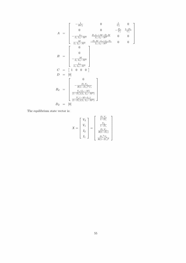
A =
− 1RC2
0 1C2
0
0 0 −Ds
C1
1−Ds
C1
− L1
L1 L2−M2
DsL1+M−DsML1 L2−M2 0 0
ML1 L2−M2
−DsM−L2+L2 Ds
L1 L2−M2 0 0
B =
0
0
− ML1 L2−M2
L2
L1 L2−M2
C =[
1 0 0 0]
D = [0]
Bd =
0
−DsVg
R(1−Ds)2C1
Vg (L1−M)(1−Ds)(L1 L2−M2)
Vg (−M+L2 )(1−Ds)(L1 L2−M2)
Dd = [0]
The equilibrium state vector is:
X =
V2
V1
I2
I1
=
DsVg
1−Ds
Vg
1−Ds
DsVg
R(1−Ds)
Ds2Vg
R(1−Ds)2
55
Bibliography
[1] G. C. Verghese, “Dynamic modeling and control in power electronics,” in The Control Handbook, W. S.Levine, Ed. Boca Raton, FL: CRC Press LLC, 1996, ch. 78.1, pp. 1413–1424.
[2] R. T. Stefani, B. Shahian, C. J. Savant, Jr., and G. H. Hostetter, Design of Feedback Control Systems,4th ed. New York, NY: Oxford University Press, 2002.
[3] D. Graham and R. C. Lathrop, “The synthesis of optimum transient response: Criteria and standardforms,” Trans. AIEE, vol. 72, pp. 273–288, Nov. 1953.
[4] B. N. Datta, Numerical Methods for Linear Control Systems. San Diego, CA: Elsevier Academic Press,2004.
[5] R. C. Dorf and R. H. Bishop, Modern Control Systems, 10th ed. Upper Saddle River, NJ: PearsonPrentice Hall, 2005.
[6] B. D. O. Anderson and J. B. Moore, Optimal Control: Linear Quadratic Methods. Englewood Cliffs,NJ: Prentice Hall, Inc., 1990.
[7] G. M. Siouris, An Engineering Approach to Optimal Control and Estimation Theory. New York, NY:Wiley, 1996.
[8] J. C. Doyle, “Guaranteed margins for LQG regulators,” IEEE Trans. Automat. Contr., vol. 23, pp.756–757, Aug. 1978.
[9] J. C. Doyle and G. Stein, “Robustness with observers,” IEEE Trans. Automat. Contr., vol. 24, pp.607–611, Aug. 1979.
[10] B. M. Chen, “Theory of loop transfer recovery for multivariable linear systems,” Ph.D. dissertation,Washington State Univ., Pullman, WA, Dec. 1991.
[11] A. Saberi and P. Sannuti, “Observer design for loop transfer recovery and for uncertain dynamicalsystems,” IEEE Trans. Automat. Contr., vol. 35, pp. 878–897, Aug. 1990.
[12] G. Stein and M. Athans, “The LQG/LTR procedure for multivariable feedback control design,” IEEETrans. Automat. Contr., vol. 32, pp. 105–114, Feb. 1987.
[13] B. Friedland, Control System Design: An Introduction to State-Space Methods. New York, NY:McGraw-Hill, 1986.
[14] MATLAB Control Systems Toolbox 6.0 User’s Guide, The Mathworks, 2004.
[15] R. S. Sanchez-Pena and M. Sznaier, Robust Systems: Theory and Applications. New York, NY: Wiley,1998.
[16] A. N. Madiwale and D. E. Williams, “Some extensions of loop transfer recovery,” in Proc. of theAmerican Control Conference (ACC’85), Boston, MA, June 1985, pp. 790–795.
[17] R. C. Jaeger, Microelectronic Circuit Design. Boston, MA: McGraw-Hill, 1997.
[18] W. J. Palm, Control Systems Engineering. New York, NY: Wiley, 1986.
56