modelling digital logic in sdl - springer · modelling digital logic in sdl 371 flip-flops,...
TRANSCRIPT

23 Modelling Digital Logic in SDL
G. Csopaki•, and K. j. Turner"
•Department of Telecommunications and Telematics, Technical University of Budapest
H-1521 Budapest, Hungary (Email: [email protected])
"Department of Computing Science and Mathematics, University of Stirling Stirling FK9 4LA, Scotland (Email: [email protected])
Abstract
The specification of digital logic in SOL (Specification and Description Language) is investigated. A specification approach is proposed for multi-level descriptions of hardware behaviour and structure. The modelling method exploits features introduced in SDL-92. The approach also deals with the specification, analysis and simulation of timing aspects at any level in the specification of digital logic.
Keywords: Digital Logic, Hardware Design, SOL (Specification and Description Language), Timing Analysis.
1. Introduction
1.1 Application of SOL
This paper addresses the specification and validation of digital logic components and digital systems using SDL-92 (Specification and Description Language [1,2,3]). SOL was developed by CCITI/ITU-T in the context of telecommunications. ETSI (European Telecommunications Standards Institute) has defined a methodology for preparing standards and reports that describe certain kinds of system (communications protocols or services) whose behaviour is mainly discrete and consists of actions in response to signals or other inputs. The main technique in this methodology for defming behaviour (and associated structure) is SOL. Data is defmed using SOL combined with ASN.1 (Abstract Syntax Notation 1 [4]). An SDL description has companion descriptions using ASN.l and MSCs (Message Sequence Charts [5]). The result has no informal text and is consistent, unambiguous and precise. A combined description can be validated with software tools.
SDL has been widely used to specify and validate communications protocols and communications systems. Nonetheless, SDL is a general-purpose language that is appropriate for many other applications. For example, it has been used in general software design and for real-time systems. Surprisingly, the use of SDL to describe hardware seems to have been rather limited. Hardware description with SDL has evolved in studies of hardware-software co-design [6, 7]. This paper investigates how SOL can be used for the specification and
Formal Description Techniques and Protocol Specification, Testing and Verification T . Mizuno, N. Shiratori, T. Higashino & A. Togashi (Eds.) © 1997 IFIP. Published by Chapman & Hall

368 Part Seven Languages and Applications
analysis of digital systems. In fact it is permissible to realise system components using hardware or software, so co-design is also possible.
1.2 Digital Logic Design
Digital logic design is partly top-down and partly bottom-up. The general approach is topdown. but designers exploit available components and designs. Components are specified and manufactured to defined interfaces, or sometimes standards. A well-defined specification is the basis of verification and validation. Such a specification should completely cover the required functional behaviour, should quantify time delays inside components, and should exhibit a clear structure of components and their interconnections.
Top-down logic design proceeds in the following way. The user begins by describing the expected behaviour of a functional unit and its timing characteristics. This black-box description is called a functional specification. and refers only to inputs and outputs. The user now has to describe the proposed design structure using functional specifications of its components and their interconnections. At this point the behaviour and properties of the functional unit can be investigated, perhaps by simulation using sample input data sequences. If the proposed design fulfils its requirements. the procedure can be repeated recursively for the subsidiary components. The design process is complete when components are ready-made ones with known characteristics. Design efficiency is improved when verified or validated functional specifications are stored in a library for use by all designers.
1.3 Hardware Description Languages
Digital logic and digital system design arc well developed topics. Many textbooks explain the operation of logic gates and other functional elements, and explain how to combine them into larger circuits and systems. Digital logic design uses elements that are available as hardware components from the manufacturer's catalogue [8].
Hardware Description Languages have been extensively studied. Languages such as VHDL (VLSI Hardware Description Language [9)), ClRCAL (Circuit Calculus [10]), CARS [II] and many others have been used to specify and analyse digital hardware. Like SDL, LOTOS (Language Of Temporal Ordering Specification [12]) was developed for describing communications systems. The inspiration for the work reported in this paper was the LOTOS-based approach called DILL (Digital Logic in LOTOS (13]).
DILL supports the hardware engineer when translating a circuit schematic into a LOTOS specification. The DILL library contains a variety of pre-defined components such as might be obtained off-the-shelf. Translation into DILL allows properties of a circuit to be investigated. Once the specification has been verified or validated, it can be realised as actual hardware. The designer must be familiar to some extent with LOTOS so as to combine behaviour expressions. but this is reasonably straightforward and does not require an in-depth knowledge of LOTOS.
The approach of this paper is named ANISEED (Analysis In SDL Enhancing Electronic Design) - somewhat similar to DILL except that the specification language is SDL. Since SDL is widely used in industry and is well supported by commercial tools. it is hoped that the approach will be attractive to electronics engineers. The designer needs only a basic knowledge of SDL in order to describe and analyse circuits. Libraries in the form of SDL packages supply ready-made circuit components and design structures. These present solutions in a form that is familiar to the electronics engineer.

Modelling digital logic in SDL 369
2. Digital Logic Specification with SDL
2.1 Description of Behaviour
The behaviour of a functional unit is given by an SDL description. Process types are used to represent generic components; actual components are instances of these. Component descriptions are stored in a library as SDL-92 named packages. When the generic definition of a component is instantiated, its parameters arc set to describe the characteristics of the particular instance. Parameters will include the names of input and output signals, as well as timing characteristics such as propagation delays.
It is highly desirable to have descriptions of logic designs at different levels of abstraction. For example, a low-level description might be appropriate for fabrication or validation of a component. However, once the low-level design has been proven it may be used as a building brick in higher level designs. That is, it may be treated as black box whose internal structure is unimportant at the chosen level of abstraction. A component may thus have several descriptions in a library, to be selected by the designer as appropriate.
The approach deals only with discrete signals, but it handles continuous signals implicitly by modelling their changes (i.e. the signal edges). Hardware signals are modelled as SDL signals with two parameters: the time when the signal is generated, and the binary logic value. The time value of an input signal records when it was generated. The time value is used to determine the time of possible output signals (according to the time delay inherent in a component). The logic value of a signal may be a single bit, but for generality a vector of bits may be used. This caters for common situations such as an address bus or control bus that is several bits wide. ln a high-level description. a signal could even carry an SDL data structure, allowing for an abstract description of the interface to a component
Time delays are often significant in the design of digital logic- especially in asynchronous circuits. It is important that the designer be able to state propagation delays and timing restrictions explicitly. Timing information appears in process parameters and in signals. A process type can be instantiated with different timing values to reflect technology variations or differences due to fan-out of a component. The unit of time in an SDL description is at the discretion of the specifier. Integer time values are used in this work, with a typical interpretation being nanoseconds.
The wires of a circuit are normally considered to carry signals instantaneously between components. Of course this is not strictly true, but the transmission time over a wire is usually negligible compared to the reaction time of a component. ln high-speed circuits, a wire can be modelled as a delay if necessary. ln digital hardware, the wires between components usually carry signals only in one direction. However bidirectional signals are possible, for example over a bus. The SDL processes representing components are connected by zero-delay channels representing the wires. As usual, channels can be unidirectional or bidirectional.
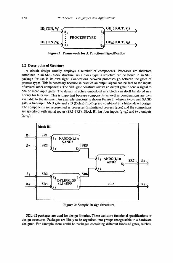
Process types may have many input and output gates. Figure 1 shows a component described as a functional unit by an SDL process. The input signals are IE, to IE, and the output signals are OEi to OE •. The signals carry a time (TlN or TOUT) and a value (V, to V;).
370 Part Seven La11guages a11d Applicatioll.l"
lEt (TIN, Vt) , ~j
OEj(TOUT, Vj) ' , ~1 /
PROCESS TYPE IE;(TIN ,V;) ,
gi OE0 (TOUT, Vn) -" g'l /
Figure 1: Framework for A Functional Specification
2.2 Description of Structure
A circuit design usually employs a number of components. Processes are therefore combined in an SOL block structure. As a block type, a structure can be stored in an SDL package for use in its own right. Connections between processes go between the gates of process types. This is necessary because in practice an output signal can be sent to the inputs of several other components. The SDL gate construct allows an output gate to send a signal to one or more input gates. The design structure embedded in a block can itself be stored in a library for later use. This is important because components as well as combinations are then available to the designer. An example structure is shown Figure 2, where a two-input NAND gate, a two-input AND gate and a D (Delay) flip-flop are combined in a higher-level design. The components are represented as processes (instantiated process types) and the connections are specified with signal routes (SR l-SR8). Block B I has four inputs (g,-g,) and two outputs (g,-g.).
block Bl
gl SRI gl NANDG(l,l):
NAND2 g2
' SR2 , SRS
h g3
7 gl ANDG(l,l): SR7 , gs ' AND2 g3 / /
7 g2
g3 SR3, SR6 ' /
/ g 1 DFLIPFLOP g
g4 '
SR4, (l,l):DFF SRS ' g6'
/ g2 g ,
Figure 2: Sample Design Structure
SDL-92 packages are used for design libraries. These can store functional specifications or design structures. Packages are likely to be organised into groups recognisable to a hardware designer. For example there could be packages containing different kinds of gates, latches,

Modelling digital logic in SDL 371
flip-flops, counters, registers and so on. Because package elements are parameterised, they represent a variety of instances (implementations) of components and structures
3. Modelling Functional Units
The behaviour of functional units is given by process types. In general, signals carry time and value parameters. As a degenerate case, the time parameter of a signal may be omitted when timing characteristics are not significant. This is appropriate for synchronous logic, where output signals are enabled by clock pulses. In synchronous circuits, component delays can be ignored since it is assumed that the reaction time of a component is faster than the clock rate. But in an asynchronous (unclocked) circuit, exact knowledge of component delays may be necessary to avoid race conditions. Correct operation in the presence of timing constraints may be checked through simulation or through proof of correctness. For adequate modelling it should be possible to:
• give a functional specification of behaviour at any level of abstraction
• define a design structure as a collection of components (process types given in packages) and their interconnection
• have multi-level descriptions, i.e. treat a component as a black box or as a structure containing a finer level of detail
• specify timing characteristics at any level of abstraction.
3.1 Logic Sources and Sinks
Some aspects of logic design require special process types in the SDL. Sometimes it is necessary to specify a source of logic 0 or I, say to tie an input to a specific level. This is a nullary logic function, specified by process types ZERO and ONE that provide logic 0 and 1 respectively. It may also be necessary to specify a source of other constant values (e.g. some binary input vector). The CONSTANT process type provides a constant output given by its parameter value. Logic sources generate their constants signals at simulation time zero.
1f the output of a component is not connected to anything, process output signals have to be consumed but not used. The ABSORB process type is ready to accept and absorb any signal. Note that this differs from standard hardware design: if an output of a component is unused, the engineer simply does not connect anything to it. However, the corresponding SDL process must have a route for output signals to follow (even if nothing is done with them). With a little pre-processing, the use of ABSORB could be made invisible to the specifier. Nonetheless. it could be argued that it is desirable to force an explicit choice of what to do with each output. If an output is accidentally left unconnected, it is useful that a check of the corresponding SDL should point out the error.
3.2 Basic Logic Gates
Logic gates are specified as process types with signal names and gate delays as parameters. Logic gates carry signals that are simple binary (bit) values. A real logic gate exhibits a propagation delay from a change in input to the subsequent output; this reflects the physical processes involved in moving charges into or out of the gate.
Figure 3 illustrates a two-input AND gate. Figure 3 (a) shows the conventional logic symbol for AND2 and its idealised timing diagram. Transitions between logic 0 (low) and logic I (high) are imagined to take place instantaneously. In practice, electrical signals never have a sharp edge so Figure 3 (b) is more typical of what happens. Transitions between logic levels are shown as sloping lines here since they are never instantaneous in reality. In Figure

372 Part Seven Languages and Applications
3 (b), TPDl is the delay for the output C to become valid level 1 after input A changes to l. TPDO is the delay taken for the output C to become valid level 0 after input B changes to 0. In real devices, these delays may be different because they require charges to flow in opposite directions. If the engineer does not require to make this distinction, a single delay could be used for output of a 1 or a 0.
A
B
c
Figure 3 (a): Symbol for AND2 Gate and Idealised Timing Diagram
A--""1
B--+---~
Figure 3 (b): Realistic Timing Diagram for AND2 Gate
An SDL/GR representation of the AND2 gate is given in Figure 4, using timers to specify the propagation delays. The variable OUTN represents the computed value that will be output following the delay time. Only if this differs from the current gate output OUT is it necessary to generate a signal. The delays TPDl and TPDO are given actual parameter values during instantiation. Inside the process, delays are handled by timers. When the relevant timer expires, the new output value (OU1) and the time when it is generated (TOUT) are carried by the output signal. An interesting case arises if a further input occurs while the delay timer is running. This corresponds to an input changing before the gate can react to a previous change of input. In such a case, the new output value is calculated. If this differs from the output that is pending, the revised output is scheduled instead after the required delay.

Modelling digital logic in SDL
process type AND2
I fpar TPDO, TPDl Duration; ~
del Vl, V2, OUT, OUTN Boolean:= False, TIN, TOUT Time;
I timer Tl, TO;
Figure 4: SDLIGR Description of AND2 Gate
373

374 Part Seven Languages am/ Applications
Many gates can be modelled in the same way as AND2; a different number of inputs would simply require an alteration to the input signals in the idle and wait states. To compute the new output value, the standard Boolean type and its operators are used. Most of the operators likely to be needed are available in SDL (or, xor, and, not, arithmetic operators, relational operators). However, new operators such as nand could be defmed using the normal data typing features of SDL. In fact it is possible to define a generic logic gate where the number of inputs and the Boolean function are determined by parameters. A generic gate is simply a process type with extra parameters that allow it to become a specific kind of gate -a two-input AND, four-input NOR or whatever.
The initial state of real hardware may be indefinite following power-on. This is not modelled explicitly in the SDL description, since no outputs are generated until inputs occur. However, this is not a limitation since in practice the circuit designer is forced to ensure a well-defined initial state by explicit sequences of signals. For the SDL description, this simply means that the processes will be initialised by specific input signals.
Real logic gates have a fan-out (the maximum number of other gates that can be connected to an output). Real logic gates also have a fan-in (the maximum number of inputs). These are component limitations that can be checked by static analysis of the SDL description. Since fan-out and fan-in have an effect on the delays introduced by gates, the designer can take them into account by choosing appropriate values for the process parameters TPDl and TDPO.
The wires connecting components introduce a propagation delay that is usually insignificant but can be critical in high-speed circuits. The wires can be considered as components as well, represented by simple delay elements. A process type DELAY is defined for this purpose, with actual transmission delay as a parameter.
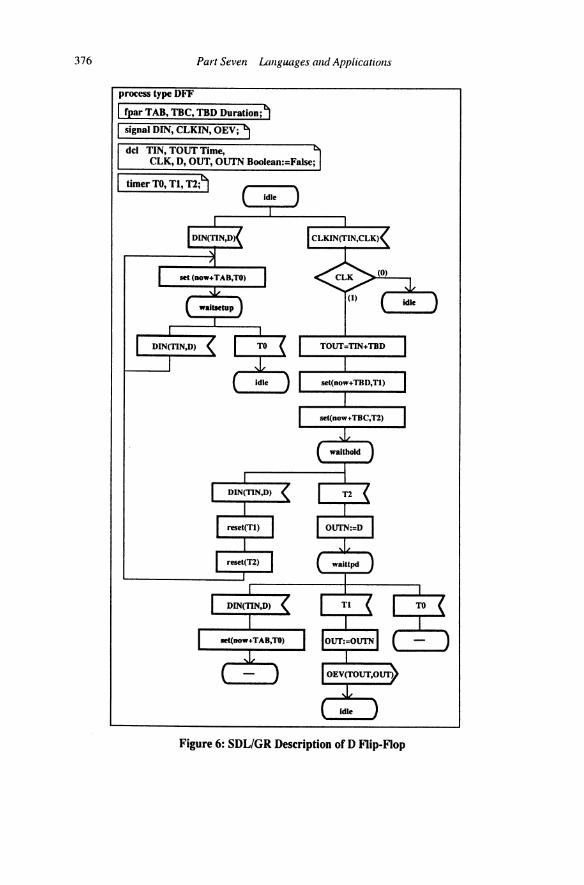
3.3 Specification of Delay Flip-Flop
AD (Delay) flip-flop stores its input (D) when a clock pulse occurs. The data will appear on the output (Q) after the next clock pulse. AD flip-flop is thus like a single-bit memory. It is useful for data storage and similar applications. Other kinds of flip-flop include the RS (Reset-Set) and JK types. Figure 5 (a) shows the logic symbol for a D flip-flop and its idealised timing diagram. At point A the D input rises to logic 1. At point B the flip-flop is clocked, so the D input is latched and transferred to the Q output.
D 1----Q
CLKIN __ --1 D flip-nop D
CLKIN
Q
A B
Figure 5 (a): Symbol for D Flip-Flop and Idealised Timing Diagram
Figure 5 (b) illustrates the likely timing behaviour of a real D flip-flop. The time between points A and B (tAB) is called the data setup time. This is measured from the point at which the D input reaches logic 1 and the point at which the clock reaches logic 1. The time is the

Modelling digital logic i11 SDL 375
minimum for which data must be stable at the input of the flip-flop before it is clocked. At point C, the logic 1 input has started to go low. The time between B and C (tBC) is called the data hold time. It is the minimum time for which the data must be held stable after the flipflop has been clocked. As a result of clocking the flip-flop, its Q output changes state at point D. The time tBD is the maximum time taken for the output to become valid following a clock pulse.
D
CLKIN
Q A B c
tAB tsc ' " data setup /'-. data hold
time time / tso _'\ ,, ,1' (lelay tJme
Figure 5 (b): Realistic Timing Diagram forD Flip-Flop
D
An SOL description of a 0 flip-flop is given in Figure 6. This follows a similar pattern to the AN02 gate given Figure 4, except that the delays are those particular to a 0 flip-flop.
3.4 Higher-Level Functional Units
Higher level functional units are frequently used in the top-down design process. These functional units are black-boxes with inputs and outputs and no internal structure. Complex functions can easily be described using the ADT facilities of SOL. Interestingly, it is unimportant whether such functions are realised as hardware or software. This makes it possible to describe mixed hardware-software systems within the same framework. If the designer wishes to specify functional behaviour at an abstract level, it is usually irrelevant whether the realisation is in hardware or software.
Consider, for example, a floating point arithmetic unit. This could be realised as hardware (a co-processor) or as software (by emulation of missing hardware instructions). The designer merely has to specify the interfaces of the functional unit, including input and output data (structures) and timing constraints. At this level of abstraction, a functional unit can be a hardware or software element (and indeed both realisations may be available). Hardware/software functional units can cooperate through signals sent via channels and signal routes. For an abstract description, a signal could carry a data structure such as the content of a data register or address register. Timing characteristics can be given even if the realisation will be in software.
376 Part Seven Languages and Applications
process type DFF
I fpar TAB, TBC, TBD Duration;~ I signal DIN, CLKIN, OEV; ~
del TIN, TOUT Time, CLK, D, OUT, OUTN Boolean:=False;
timer TO, Tl, T2;~
Figure 6: SDL/GR Description of D Flip-Flop

Modelling digital logic in SDL 377
As a concrete example, Figure 7 shows a BCD (Binary Coded Decimal) full adder as a high-level functional unit. AIN and BIN each convey four input bits representing BCD digits from 0 to 9. CIN and COUT are one-bit carry-in and carry-out signals. SOUT conveys BCD sum output in four bits.
:: ---~~~-8-~-~-d-~~-~~-~:=====:: ::: Figure 7: BCD Full Adder as A Black Box
The functional behaviour of this high-level description is given in Figure 8. The value TPDS is the addition delay time - the time from an input change to the change in SOUT. The value TPDCO is the carry delay time for a change in COUT.
The BCD full adder could easily be realised as software, but a hardware implementation will be considered here. The design (internal details of the black box) can be found in any standard textbook on computer logic. Readers unfamiliar with the conventional design should note that it uses the 'trick' of adding 6 (binary 0110) to the first input A. The BCDF block in Figure 9 comprises processes connected via channels between the gates. A, B and SOUT are four-bit hexadecimal values, while CIN and COUT are just one bit. ADD! , ADD2 and ADD3 are instances of the BCD ADDER four-bit binary full adder. INVl is an instance of the FINV four-bit output special inverter. (Of course, BCDADDER and FINV would be found in the component libraries.) The design also requires the special ZERO, ABSORB and CONSTANT process types introduced in Section 3.1. Zl is used to feed logic 0 to the carry input of ADD! and ADD2. SIX is used to feed the constant bit vector 0110 to the second input of ADDl. Since the carry outputs of ADD! and ADD3 are not required, they are absorbed by A 1.
4. Validation and Simulation
Validation of a circuit design represented in SDL is conducted through simulation. Although SDL has a formal basis and could thus be used for verification, in practice it is usual to treat verification of SDL descriptions as being exhaustive simulation. Simulation may be an interactive walk through every significant path in order to gain confidence in the design. Step-by-step simulation allows concentration on fewer signals. Another method is to store pre-defmed input sequences in a file that is read by the simulator. This is particularly suitable for regression testing, when a design change must be shown to have respected previous behaviour. Simulation results can be presented using MSC sequences, which gives the designer a convenient graphical overview of the behaviour.

378 Part Seven Languages and Applications
process type BCDF
I fpar TPDS, TPDCO Duration; ~ I signal AIN, BIN, CIN, SOUT, COUT; ~ • r del TIN, TCO, TSO Time, I;~
A, B, C, S, CO, SN, CON Naturai:=O;
ltimerT, Tl; ~ ( )
·~ ( Idle ) r
IAIN(A,TIN)( I BIN(B,TIN) ( I CIN(c,nN>(
I SN:=(A+B+C)modiO I r TSO:=TIN+ TPDS I
r set( DOW+ TPDS,TI l
~ .. ~.1 r CON:=l I r CON:=O I
17 I'
I TCO:=TIN+ TPDCO
I
I I set( DOW+ TPDCO,TI) I
J ( w•it l
I I
I T ( I TJ ( !
r S:=SON l I CO::CON .I 1 I
I SOIIT(S,TSO) I COIIT(CO,TCO)
l ~ ( Idle l ( wl )
I T ( I
Figure 8: SDL/GR High-Level Description of BCDF Process Type

Modelling digital logic in SOL 379
block BCDF
' / COUT
ADDl(l,l): Sl rl AOOJ(I,I): S ,CI BCDF Cl ncm·
COl--A ~OJ A 8
SOUT
T I'
s v A00'"" 1,1 ' --11 BCDF Al(l,l): ,x INVI(I,I):
Cl CC ABSORB FINV J A 8 '1'
( Zl(l,l):
J [ SIX(I,l): r]
ZERO CONSTANT
CIN A II
Figure 9: Structure of BCDF Adder
Commercial simulators such as SOT [14] and OhjectGeode [15] can be used for functional analysis of a circuit design. However, they are unsuitable for simulation of timing characteristics because of the special need for event scheduling. A timing simulator has to deal properly with the time parameter in signals. In particular, incoming signals have to be stored in input queues in increasing order of the times at which the signals were generated. Titis requires the following approach that is rather similar to discrete event simulation:
• Each process needs one input event queue, but events arc stored in these queues in increasing order of time parameter.
• Channels have zero delay. • Initially all input events are evaluated for simulator time zero. This applies especially to
process types like ZERO and ONE that generate their constant signals at this point.
• The simulator clock is now set for the next significant event - the earliest time for which any signal is scheduled. All events that are due at this time are evaluated at this point. Note that the order in which events are scheduled is irrelevant because real hardware always exhibits a non-zero delay. This guards against an incorrect order of scheduling events.
• · Simulation ceases when no more signals in queues need to be scheduled or when some predefined stop condition is met.
Figure 10 summarises the timed simulation algorithm. As with a standard SOL simulator, inputs could come from a file, outputs could be stored in a file, and outputs could be represented in MSC form. However, the point of simulation is to investigate timing characteristics of a circuit design. This might include the study of race conditions, the determination of minimum and maximum reaction times, and the construction of time sequence diagrams such as those found in Figure 3 (b) and Figure 5 (b).

380 Part Seven Languages and Applications
No
Put input signals from input files to input queues of processes
Evaluate Logic Source Processes
Process input signals sheduled for actual SCT
Find next minimum time scheduled input signal
Set SCT
No
Figure 10: General Overview of Timing Simulator Algorithm
Modelling digiwllogic in SDL 381
5. Conclusions
An approach for describing digital logic in SDL has been given. From the point of view of the circuit designer, minimal knowledge of SDL is required in order to describe and analyse circuits. Libraries in the form of SDL packages supply ready-made circuit elements and design structures. These present solutions in a form that is familiar to the electronics engineer. Components may be described at several levels of abstraction, and may even be realised as hardware or software.
The approach allows behaviour to be described at several levels from the component level up to the system level. Signals carry values that may be simply bits but could be data structures (vectors of bits). Especially for asynchronous logic, signals may also carry time values that reflect when they were generated. TI1is allows description and analysis of the timing characteristics of a design. A strategy for discrete event simulation of timed circuits has been proposed, allowing timed behaviour to be investigated as well as functional behaviour. Timed simulation can also produce timing diagrams and allow critical time constraints to be checked.
Advantages of the approach include: precise design notation, automated analysis of design, checking equivalences of higMow level designs, usc of design component library, and use of a formal design notation.
The work so far shows promise, and has demonstrated that digital logic design in SDL is feasible, following standard engineering practice. Future work will include:
• developing extended libraries of components and design structures
• equivalence checking between different levels of description
• analysing performance issues
• validating timing constraints
• investigating automatic derivation of tests from descriptions
• studying hardware-software co-design in more depth
• constructing tools to support circuit description and analysis, particularly the simulation of timed behaviour.
Acknowledgements
Gyula Csopaki was supported by the British Council during the work described in this paper, and was hosted by the Department of Computing Science and Mathematics, University of Stirling, UK.
References
[l] A. Olsen, et.al. Systems Engineering Using SDL-92. North Holland, 1994. [2] ITU-T. Specification and Description Language (SDL), Recommendation Z.IOO, International Telecommunications Union, Geneva, 1994. [3] A. Sarma. Introduction to SDL-92, Computer Networks and JSDN Systems, 28 (12), 1996.
[4] L. Vehaard. An introduction to Z.l05, Computer Networks and JSDN Systems, 28 (12), 1996.

382 Part Seven Languages and Applications
[5] ITU-T. Message Sequence Chart, Recommendation Z.l20, International Telecommunications Union, Geneva, 1993. [6] V. Levin, 0. Basbugoglu, E. Bounimova and K. lnan. A bilingual specification environment for software/hardware co-design, Proc. International Symposium on Computer and Information Systems XI, Middle-East Technical University, Ankara, Turkey, 1996.
[7] J. Peeters, M. Jadoul, E. Holz, M.Wasowski, D. Witaszek and J.-P. Delpiroux. HW/SW co-design and the simulation of a multimedia application, Proc. 7th European Simulation Symposium, 1995.
[8] A. Clements. Microprocessor Systems Design, PWS-Kent Publishing Company, 1992
[9] S. Carlson. Introduction to HDL Based Design Using VHDL, Synopsis Inc.
[lO]G. A. McCaskill and G. J. Milne. Hardware description and verification using the CIRCAL system. Research Report HDV -24-92, University of Strathclyde, 1992.
[ll]G. Csopaki. Hardware description language for specification of digital systems. Periodica Polytechnica, 33 (2), 1989. [12]1SO. Information Processing - Open Systems Interconnection- LOTOS- A Formal Description Technique based on the Temporal Ordering of Observational Behaviour, ISOJIEC 8807, International Organization for Standardization, Geneva, 1989.
[13]K. J. Turner and R. 0 Sinnott. DILL: Specifying digital logic in LOTOS, in Formal Description Techniques VI, Elsevier Science B.V., 1994.
[ 14] Telelogic AB. SDT 3.1: Tutorial on SDT Tools, Malm0, Sweden, 1996. [15] Verilog. ObjectGeode Simulator Reference Manual, Toulouse, France, 1996.