mips64® architecture for programmers volume iii: the ... · violations thereof may result in...
TRANSCRIPT
Document Number: MD00091Revision 2.50July 1, 2005
MIPS Technologies, Inc.1225 Charleston Road
Mountain View, CA 94043-1353
Copyright © 2001-2003,2005 MIPS Technologies Inc. All rights reserved.
MIPS64® Architecture For ProgrammersVolume III: The MIPS64® Privileged Resource
Architecture

Copyright © 2001-2003,2005 MIPS Technologies, Inc. All rights reserved.
Unpublished rights (if any) reserved under the copyright laws of the United States of America and other countries.
This document contains information that is proprietary to MIPS Technologies, Inc. ("MIPS Technologies"). Any copying,reproducing, modifying or use of this information (in whole or in part) that is not expressly permitted in writing by MIPS Technologiesor an authorized third party is strictly prohibited. At a minimum, this information is protected under unfair competition and copyrightlaws. Violations thereof may result in criminal penalties and fines.
Any document provided in source format (i.e., in a modifiable form such as in FrameMaker or Microsoft Word format) is subject touse and distribution restrictions that are independent of and supplemental to any and all confidentiality restrictions. UNDER NOCIRCUMSTANCES MAY A DOCUMENT PROVIDED IN SOURCE FORMAT BE DISTRIBUTED TO A THIRD PARTY INSOURCE FORMAT WITHOUT THE EXPRESS WRITTEN PERMISSION OF MIPS TECHNOLOGIES, INC.
MIPS Technologies reserves the right to change the information contained in this document to improve function, design or otherwise.MIPS Technologies does not assume any liability arising out of the application or use of this information, or of any error or omissionin such information. Any warranties, whether express, statutory, implied or otherwise, including but not limited to the impliedwarranties of merchantability or fitness for a particular purpose, are excluded. Except as expressly provided in any written licenseagreement from MIPS Technologies or an authorized third party, the furnishing of this document does not give recipient any licenseto any intellectual property rights, including any patent rights, that cover the information in this document.
The information contained in this document shall not be exported, reexported, transferred, or released, directly or indirectly, inviolation of the law of any country or international law, regulation, treaty, Executive Order, statute, amendments or supplementsthereto. Should a conflict arise regarding the export, reexport, transfer, or release of the information contained in this document, thelaws of the United States of America shall be the governing law.
The information contained in this document constitutes one or more of the following: commercial computer software, commercialcomputer software documentation or other commercial items. If the user of this information, or any related documentation of anykind, including related technical data or manuals, is an agency, department, or other entity of the United States government("Government"), the use, duplication, reproduction, release, modification, disclosure, or transfer of this information, or any relateddocumentation of any kind, is restricted in accordance with Federal Acquisition Regulation 12.212 for civilian agencies and DefenseFederal Acquisition Regulation Supplement 227.7202 for military agencies. The use of this information by the Government is furtherrestricted in accordance with the terms of the license agreement(s) and/or applicable contract terms and conditions covering thisinformation from MIPS Technologies or an authorized third party.
MIPS, MIPS I, MIPS II, MIPS III, MIPS IV, MIPS V, MIPS-3D, MIPS16, MIPS16e, MIPS32, MIPS64, MIPS-Based, MIPSsim,MIPSpro, MIPS Technologies logo, MIPS RISC CERTIFIED POWER logo, 4K, 4Kc, 4Km, 4Kp, 4KE, 4KEc, 4KEm, 4KEp, 4KS,4KSc, 4KSd, M4K, 5K, 5Kc, 5Kf, 20Kc, 24K, 24Kc, 24Kf, 24KE, 24KEc, 24KEf, 25Kf, 34K, R3000, R4000, R5000, ASMACRO,Atlas, "At the core of the user experience.", BusBridge, CorExtend, CoreFPGA, CoreLV, EC, FastMIPS, JALGO, Malta, MDMX,MGB, PDtrace, the Pipeline, Pro Series, QuickMIPS, SEAD, SEAD-2, SmartMIPS, SOC-it, and YAMON are trademarks orregistered trademarks of MIPS Technologies, Inc. in the United States and other countries.
All other trademarks referred to herein are the property of their respective owners.
MIPS64® Architecture For Programmers Volume III, Revision 2.50
Copyright © 2001-2003,2005 MIPS Technologies Inc. All rights reserved.
Template: B1.14, Built with tags: 2B ARCH FPU_PS FPU_PSandARCH MIPS64
MIPS64® Architecture For Programmers Volume III, Revision 2.50 i
Copyright © 2001-2003,2005 MIPS Technologies Inc. All rights reserved.
Table of Contents
Chapter 1 About This Book ................................................................................................................................................. 11.1 Typographical Conventions ................................................................................................................................... 1
1.1.1 Italic Text ..................................................................................................................................................... 11.1.2 Bold Text ..................................................................................................................................................... 11.1.3 Courier Text ................................................................................................................................................. 1
1.2 UNPREDICTABLE and UNDEFINED ................................................................................................................ 21.2.1 UNPREDICTABLE ..................................................................................................................................... 21.2.2 UNDEFINED ............................................................................................................................................... 21.2.3 UNSTABLE ................................................................................................................................................. 2
1.3 Special Symbols in Pseudocode Notation .............................................................................................................. 31.4 For More Information ............................................................................................................................................ 5
Chapter 2 The MIPS64 Privileged Resource Architecture .................................................................................................. 72.1 Introduction ............................................................................................................................................................ 72.2 The MIPS Coprocessor Model ............................................................................................................................... 7
2.2.1 CP0 - The System Coprocessor ................................................................................................................... 72.2.2 CP0 Registers ............................................................................................................................................... 7
Chapter 3 MIPS64 Operating Modes ................................................................................................................................... 93.1 Debug Mode .......................................................................................................................................................... 93.2 Kernel Mode .......................................................................................................................................................... 93.3 Supervisor Mode .................................................................................................................................................... 93.4 User Mode ............................................................................................................................................................ 103.5 Other Modes ......................................................................................................................................................... 10
3.5.1 64-bit Address Enable ................................................................................................................................ 103.5.2 64-bit Operations Enable ........................................................................................................................... 103.5.3 64-bit Floating Point Operations Enable .................................................................................................... 103.5.4 64-bit FPR Enable ...................................................................................................................................... 113.5.5 Coprocessor 0 Enable ................................................................................................................................ 11
Chapter 4 Virtual Memory ................................................................................................................................................. 134.1 Support in Release 1 and Release 2 of the Architecture ...................................................................................... 13
4.1.1 Virtual Memory ......................................................................................................................................... 134.1.2 Physical Memory ....................................................................................................................................... 13
4.2 Terminology ......................................................................................................................................................... 134.2.1 Address Space ............................................................................................................................................ 134.2.2 Segment and Segment Size (SEGBITS) .................................................................................................... 144.2.3 Physical Address Size (PABITS) ............................................................................................................... 14
4.3 Virtual Address Spaces ........................................................................................................................................ 144.4 Compliance .......................................................................................................................................................... 174.5 Access Control as a Function of Address and Operating Mode .......................................................................... 174.6 Address Translation and Cache Coherency Attributes for the kseg0 and kseg1 Segments ................................. 194.7 Address Translation and Cache Coherency Attributes for the xkphys Segment ................................................. 194.8 Address Translation for the kuseg Segment when StatusERL = 1 ...................................................................... 224.9 Special Behavior for the kseg3 Segment when DebugDM = 1 ........................................................................... 224.10 Special Behavior for Data References in User Mode with StatusUX = 0 ......................................................... 224.11 TLB-Based Virtual Address Translation ........................................................................................................... 23
4.11.1 Address Space Identifiers (ASID) ........................................................................................................... 234.11.2 TLB Organization .................................................................................................................................... 234.11.3 TLB Initialization ..................................................................................................................................... 244.11.4 Address Translation ................................................................................................................................. 26
ii MIPS64® Architecture For Programmers Volume III, Revision 2.50
Copyright © 2001-2003,2005 MIPS Technologies Inc. All rights reserved.
Chapter 5 Interrupts and Exceptions .................................................................................................................................. 315.1 Interrupts .............................................................................................................................................................. 31
5.1.1 Interrupt Modes .......................................................................................................................................... 325.1.2 Generation of Exception Vector Offsets for Vectored Interrupts .............................................................. 39
5.2 Exceptions ............................................................................................................................................................ 415.2.1 Exception Vector Locations ....................................................................................................................... 415.2.2 General Exception Processing ................................................................................................................... 435.2.3 EJTAG Debug Exception .......................................................................................................................... 455.2.4 Reset Exception ......................................................................................................................................... 455.2.5 Soft Reset Exception .................................................................................................................................. 475.2.6 Non Maskable Interrupt (NMI) Exception ............................................................................................... 485.2.7 Machine Check Exception ......................................................................................................................... 485.2.8 Address Error Exception ............................................................................................................................ 495.2.9 TLB Refill and XTLB Refill Exceptions ................................................................................................... 505.2.10 TLB Invalid Exception ............................................................................................................................ 505.2.11 TLB Modified Exception ......................................................................................................................... 515.2.12 Cache Error Exception ............................................................................................................................. 515.2.13 Bus Error Exception ................................................................................................................................. 525.2.14 Integer Overflow Exception ..................................................................................................................... 525.2.15 Trap Exception ......................................................................................................................................... 535.2.16 System Call Exception ............................................................................................................................. 535.2.17 Breakpoint Exception ............................................................................................................................... 535.2.18 Reserved Instruction Exception ............................................................................................................... 545.2.19 Coprocessor Unusable Exception ............................................................................................................ 545.2.20 MDMX Unusable Exception ................................................................................................................... 555.2.21 Floating Point Exception ......................................................................................................................... 555.2.22 Coprocessor 2 Exception ......................................................................................................................... 565.2.23 Watch Exception ...................................................................................................................................... 565.2.24 Interrupt Exception .................................................................................................................................. 56
Chapter 6 GPR Shadow Registers ...................................................................................................................................... 596.1 Introduction to Shadow Sets ................................................................................................................................ 596.2 Support Instructions ............................................................................................................................................. 60
Chapter 7 CP0 Hazards ...................................................................................................................................................... 617.1 Introduction .......................................................................................................................................................... 617.2 Types of Hazards ................................................................................................................................................. 61
7.2.1 Execution Hazards ..................................................................................................................................... 617.2.2 Instruction Hazards .................................................................................................................................... 62
7.3 Hazard Clearing Instructions and Events ............................................................................................................. 637.3.1 Instruction Encoding .................................................................................................................................. 64
Chapter 8 Coprocessor 0 Registers .................................................................................................................................... 658.1 Coprocessor 0 Register Summary ........................................................................................................................ 658.2 Notation ................................................................................................................................................................ 698.3 Writing CPU Registers ......................................................................................................................................... 708.4 Index Register (CP0 Register 0, Select 0) ............................................................................................................ 718.5 Random Register (CP0 Register 1, Select 0) ....................................................................................................... 728.6 EntryLo0, EntryLo1 (CP0 Registers 2 and 3, Select 0) ....................................................................................... 738.7 Context Register (CP0 Register 4, Select 0) ........................................................................................................ 788.8 PageMask Register (CP0 Register 5, Select 0) .................................................................................................... 798.9 PageGrain Register (CP0 Register 5, Select 1) .................................................................................................... 818.10 Wired Register (CP0 Register 6, Select 0) ......................................................................................................... 838.11 HWREna Register (CP0 Register 7, Select 0) ................................................................................................... 848.12 BadVAddr Register (CP0 Register 8, Select 0) ................................................................................................. 858.13 Count Register (CP0 Register 9, Select 0) ......................................................................................................... 86
MIPS64® Architecture For Programmers Volume III, Revision 2.50 iii
Copyright © 2001-2003,2005 MIPS Technologies Inc. All rights reserved.
8.14 Reserved for Implementations (CP0 Register 9, Selects 6 and 7) ..................................................................... 868.15 EntryHi Register (CP0 Register 10, Select 0) .................................................................................................... 878.16 Compare Register (CP0 Register 11, Select 0) .................................................................................................. 908.17 Reserved for Implementations (CP0 Register 11, Selects 6 and 7) ................................................................... 908.18 Status Register (CP Register 12, Select 0) ......................................................................................................... 918.19 IntCtl Register (CP0 Register 12, Select 1) ....................................................................................................... 998.20 SRSCtl Register (CP0 Register 12, Select 2) ................................................................................................... 1018.21 SRSMap Register (CP0 Register 12, Select 3) ................................................................................................ 1048.22 Cause Register (CP0 Register 13, Select 0) ..................................................................................................... 1058.23 Exception Program Counter (CP0 Register 14, Select 0) ................................................................................ 110
8.23.1 Special Handling of the EPC Register in Processors That Implement the MIPS16e ASE .................... 1108.24 Processor Identification (CP0 Register 15, Select 0) ....................................................................................... 1118.25 EBase Register (CP0 Register 15, Select 1) .................................................................................................... 1128.26 Configuration Register (CP0 Register 16, Select 0) ........................................................................................ 1148.27 Configuration Register 1 (CP0 Register 16, Select 1) ..................................................................................... 1168.28 Configuration Register 2 (CP0 Register 16, Select 2) ..................................................................................... 1208.29 Configuration Register 3 (CP0 Register 16, Select 3) ..................................................................................... 1238.30 Reserved for Implementations (CP0 Register 16, Selects 6 and 7) ................................................................. 1268.31 Load Linked Address (CP0 Register 17, Select 0) .......................................................................................... 1278.32 WatchLo Register (CP0 Register 18) ............................................................................................................... 1288.33 WatchHi Register (CP0 Register 19) ............................................................................................................... 1308.34 XContext Register (CP0 Register 20, Select 0) ............................................................................................... 1328.35 Reserved for Implementations (CP0 Register 22, all Select values) ............................................................... 1348.36 Debug Register (CP0 Register 23) ................................................................................................................... 1358.37 DEPC Register (CP0 Register 24) ................................................................................................................... 136
8.37.1 Special Handling of the DEPC Register in Processors That Implement the MIPS16e ASE ................. 1368.38 Performance Counter Register (CP0 Register 25) ........................................................................................... 1378.39 ErrCtl Register (CP0 Register 26, Select 0) ..................................................................................................... 1418.40 CacheErr Register (CP0 Register 27, Select 0) ................................................................................................ 1428.41 TagLo Register (CP0 Register 28, Select 0, 2) ................................................................................................ 1438.42 DataLo Register (CP0 Register 28, Select 1, 3) ............................................................................................... 1448.43 TagHi Register (CP0 Register 29, Select 0, 2) ................................................................................................ 1458.44 DataHi Register (CP0 Register 29, Select 1, 3) ............................................................................................... 1468.45 ErrorEPC (CP0 Register 30, Select 0) ............................................................................................................. 147
8.45.1 Special Handling of the ErrorEPC Register in Processors That Implement the MIPS16e ASE ........... 1478.46 DESAVE Register (CP0 Register 31) .............................................................................................................. 148
Appendix A Alternative MMU Organizations ................................................................................................................. 149A.1 Fixed Mapping MMU ........................................................................................................................................ 149
A.1.1 Fixed Address Translation ....................................................................................................................... 149A.1.2 Cacheability Attributes ............................................................................................................................ 152A.1.3 Changes to the CP0 Register Interface .................................................................................................... 153
A.2 Block Address Translation ................................................................................................................................. 153A.2.1 BAT Organization .................................................................................................................................... 153A.2.2 Address Translation ................................................................................................................................. 154A.2.3 Changes to the CP0 Register Interface ................................................................................................... 155
Appendix B Revision History .......................................................................................................................................... 157
iv MIPS64® Architecture For Programmers Volume III, Revision 2.50
Copyright © 2001-2003,2005 MIPS Technologies Inc. All rights reserved.
List of Figures
Figure 4-1: Virtual Address Spaces................................................................................................................................... 15Figure 4-2: Address Interpretation for the xkphys Segment ............................................................................................. 20Figure 4-3: Contents of a TLB Entry ................................................................................................................................ 24Figure 5-1: Interrupt Generation for Vectored Interrupt Mode......................................................................................... 36Figure 5-2: Interrupt Generation for External Interrupt Controller Interrupt Mode.......................................................... 38Figure 8-1: Index Register Format .................................................................................................................................... 71Figure 8-2: Random Register Format................................................................................................................................ 72Figure 8-3: EntryLo0, EntryLo1 Register Format in Release 1 of the Architecture ......................................................... 73Figure 8-4: EntryLo0, EntryLo1 Register Format in Release 2 of the Architecture ......................................................... 74Figure 8-5: Context Register Format................................................................................................................................. 78Figure 8-6: PageMask Register Format............................................................................................................................. 79Figure 8-7: PageGrain Register Format ............................................................................................................................ 81Figure 8-8: Wired And Random Entries In The TLB ....................................................................................................... 83Figure 8-9: Wired Register Format ................................................................................................................................... 83Figure 8-10: HWREna Register Format............................................................................................................................ 84Figure 8-11: BadVAddr Register Format.......................................................................................................................... 85Figure 8-12: Count Register Format.................................................................................................................................. 86Figure 8-13: EntryHi Register Format .............................................................................................................................. 87Figure 8-14: Compare Register Format............................................................................................................................. 90Figure 8-15: Status Register Format.................................................................................................................................. 91Figure 8-16: IntCtl Register Format .................................................................................................................................. 99Figure 8-17: SRSCtl Register Format ............................................................................................................................. 101Figure 8-18: SRSMap Register Format ........................................................................................................................... 104Figure 8-19: Cause Register Format................................................................................................................................ 105Figure 8-20: EPC Register Format .................................................................................................................................. 110Figure 8-21: PRId Register Format ................................................................................................................................. 111Figure 8-22: EBase Register Format ............................................................................................................................... 112Figure 8-23: Config Register Format .............................................................................................................................. 114Figure 8-24: Config1 Register Format ............................................................................................................................ 116Figure 8-25: Config2 Register Format ............................................................................................................................ 120Figure 8-26: Config3 Register Format ............................................................................................................................ 123Figure 8-27: LLAddr Register Format ............................................................................................................................ 127Figure 8-28: WatchLo Register Format .......................................................................................................................... 128Figure 8-29: WatchHi Register Format ........................................................................................................................... 130Figure 8-30: XContext Register Format.......................................................................................................................... 132Figure 8-31: Performance Counter Control Register Format.......................................................................................... 137Figure 8-32: Performance Counter Counter Register Format ......................................................................................... 139Figure 8-33: ErrorEPC Register Format.......................................................................................................................... 147Figure 8-34: Memory Mapping when ERL = 0............................................................................................................... 151Figure 8-35: Memory Mapping when ERL = 1............................................................................................................... 152Figure 8-36: Config Register Additions .......................................................................................................................... 153Figure 8-37: Contents of a BAT Entry ............................................................................................................................ 154
MIPS64® Architecture For Programmers Volume III, Revision 2.50 v
Copyright © 2001-2003,2005 MIPS Technologies Inc. All rights reserved.
List of Tables
Table 1-1: Symbols Used in Instruction Operation Statements .......................................................................................... 3Table 4-1: Virtual Memory Address Spaces ..................................................................................................................... 16Table 4-2: Address Space Access and TLB Refill Selection as a Function of Operating Mode ...................................... 17Table 4-3: Address Translation and Cache Coherency Attributes for the kseg0 and kseg1 Segments............................. 19Table 4-4: Address Translation and Cacheability Attributes for the xkphys Segment ..................................................... 20Table 4-5: Physical Address Generation ........................................................................................................................... 29Table 5-1: Interrupt Modes................................................................................................................................................ 32Table 5-2: Request for Interrupt Service in Interrupt Compatibility Mode ...................................................................... 33Table 5-3: Relative Interrupt Priority for Vectored Interrupt Mode ................................................................................. 35Table 5-4: Exception Vector Offsets for Vectored Interrupts ........................................................................................... 40Table 5-5: Interrupt State Changes Made Visible by EHB ............................................................................................... 40Table 5-6: Exception Vector Base Addresses ................................................................................................................... 42Table 5-7: Exception Vector Offsets ................................................................................................................................. 42Table 5-8: Exception Vectors ............................................................................................................................................ 43Table 5-9: Value Stored in EPC, ErrorEPC, or DEPC on an Exception........................................................................... 44Table 6-1: Instructions Supporting Shadow Sets .............................................................................................................. 60Table 7-1: Execution Hazards ........................................................................................................................................... 61Table 7-2: Instruction Hazards .......................................................................................................................................... 63Table 7-3: Hazard Clearing Instructions ........................................................................................................................... 63Table 8-1: Coprocessor 0 Registers in Numerical Order .................................................................................................. 65Table 8-2: Read/Write Bit Field Notation ......................................................................................................................... 69Table 8-3: Index Register Field Descriptions.................................................................................................................... 71Table 8-4: Random Register Field Descriptions ............................................................................................................... 72Table 8-5: EntryLo0, EntryLo1 Register Field Descriptions in Release 1 of the Architecture ....................................... 73Table 8-6: EntryLo0, EntryLo1 Register Field Descriptions in Release 2 of the Architecture ....................................... 74Table 8-7: EntryLo Field Widths as a Function of PABITS.............................................................................................. 76Table 8-8: Cache Coherency Attributes ............................................................................................................................ 76Table 8-9: Context Register Field Descriptions ................................................................................................................ 78Table 8-10: PageMask Register Field Descriptions .......................................................................................................... 79Table 8-11: Values for the Mask and MaskX1 Fields of the PageMask Register ............................................................. 79Table 8-12: PageGrain Register Field Descriptions .......................................................................................................... 81Table 8-13: Wired Register Field Descriptions................................................................................................................. 83Table 8-14: HWREna Register Field Descriptions ........................................................................................................... 84Table 8-15: BadVAddr Register Field Descriptions ......................................................................................................... 85Table 8-16: Count Register Field Descriptions ................................................................................................................. 86Table 8-17: EntryHi Register Field Descriptions .............................................................................................................. 88Table 8-18: Compare Register Field Descriptions ............................................................................................................ 90Table 8-19: Status Register Field Descriptions ................................................................................................................. 91Table 8-20: IntCtl Register Field Descriptions ................................................................................................................. 99Table 8-21: SRSCtl Register Field Descriptions............................................................................................................. 101Table 8-22: Sources for new SRSCtlCSS on an Exception or Interrupt........................................................................... 102Table 8-23: SRSMap Register Field Descriptions .......................................................................................................... 104Table 8-24: Cause Register Field Descriptions ............................................................................................................... 105Table 8-25: Cause Register ExcCode Field..................................................................................................................... 108Table 8-26: EPC Register Field Descriptions ................................................................................................................. 110Table 8-27: PRId Register Field Descriptions................................................................................................................. 111Table 8-28: EBase Register Field Descriptions............................................................................................................... 112Table 8-29: Conditions Under Which EBase15..12 Must Be Zero ................................................................................. 113Table 8-30: Config Register Field Descriptions.............................................................................................................. 114Table 8-31: Config1 Register Field Descriptions............................................................................................................ 116
vi MIPS64® Architecture For Programmers Volume III, Revision 2.50
Copyright © 2001-2003,2005 MIPS Technologies Inc. All rights reserved.
Table 8-32: Config2 Register Field Descriptions............................................................................................................ 120Table 8-33: Config3 Register Field Descriptions............................................................................................................ 123Table 8-34: LLAddr Register Field Descriptions............................................................................................................ 127Table 8-35: WatchLo Register Field Descriptions .......................................................................................................... 128Table 8-36: WatchHi Register Field Descriptions .......................................................................................................... 130Table 8-37: XContext Register Fields ............................................................................................................................. 132Table 8-38: Example Performance Counter Usage of the PerfCnt CP0 Register ........................................................... 137Table 8-39: Performance Counter Control Register Field Descriptions ......................................................................... 138Table 8-40: Performance Counter Counter Register Field Descriptions......................................................................... 140Table 8-41: ErrorEPC Register Field Descriptions ......................................................................................................... 147Table 8-42: Physical Address Generation from Virtual Addresses................................................................................. 149Table 8-43: Config Register Field Descriptions.............................................................................................................. 153Table 8-44: BAT Entry Assignments .............................................................................................................................. 154
MIPS64® Architecture For Programmers Volume III, Revision 2.50 1
Copyright © 2001-2003,2005 MIPS Technologies Inc. All rights reserved.
Chapter 1
About This Book
The MIPS64® Architecture For Programmers Volume III comes as a multi-volume set.
• Volume I describes conventions used throughout the document set, and provides an introduction to the MIPS64®Architecture
• Volume II provides detailed descriptions of each instruction in the MIPS64® instruction set
• Volume III describes the MIPS64® Privileged Resource Architecture which defines and governs the behavior of theprivileged resources included in a MIPS64® processor implementation
• Volume IV-a describes the MIPS16e™ Application-Specific Extension to the MIPS64® Architecture
• Volume IV-b describes the MDMX™ Application-Specific Extension to the MIPS64® Architecture
• Volume IV-c describes the MIPS-3D® Application-Specific Extension to the MIPS64® Architecture
• Volume IV-d describes the SmartMIPS®Application-Specific Extension to the MIPS32® Architecture and is notapplicable to the MIPS64® document set
1.1 Typographical Conventions
This section describes the use of italic, bold and courier fonts in this book.
1.1.1 Italic Text
• is used for emphasis
• is used for bits, fields, registers, that are important from a software perspective (for instance, address bits used bysoftware, and programmable fields and registers), and various floating point instruction formats, such as S, D, and PS
• is used for the memory access types, such as cached and uncached
1.1.2 Bold Text
• represents a term that is being defined
• is used for bits and fields that are important from a hardware perspective (for instance, register bits, which are notprogrammable but accessible only to hardware)
• is used for ranges of numbers; the range is indicated by an ellipsis. For instance, 5..1 indicates numbers 5 through 1
• is used to emphasize UNPREDICTABLE and UNDEFINED behavior, as defined below.
1.1.3 Courier Text
Courier fixed-width font is used for text that is displayed on the screen, and for examples of code and instructionpseudocode.
2 MIPS64® Architecture For Programmers Volume III, Revision 2.50
Copyright © 2001-2003,2005 MIPS Technologies Inc. All rights reserved.
Chapter 1 About This Book
1.2 UNPREDICTABLE and UNDEFINED
The terms UNPREDICTABLE and UNDEFINED are used throughout this book to describe the behavior of theprocessor in certain cases. UNDEFINED behavior or operations can occur only as the result of executing instructionsin a privileged mode (i.e., in Kernel Mode or Debug Mode, or with the CP0 usable bit set in the Status register).Unprivileged software can never cause UNDEFINED behavior or operations. Conversely, both privileged andunprivileged software can cause UNPREDICTABLE results or operations.
1.2.1 UNPREDICTABLE
UNPREDICTABLE results may vary from processor implementation to implementation, instruction to instruction, oras a function of time on the same implementation or instruction. Software can never depend on results that areUNPREDICTABLE. UNPREDICTABLE operations may cause a result to be generated or not. If a result is generated,it is UNPREDICTABLE. UNPREDICTABLE operations may cause arbitrary exceptions.
UNPREDICTABLE results or operations have several implementation restrictions:
• Implementations of operations generating UNPREDICTABLE results must not depend on any data source (memoryor internal state) which is inaccessible in the current processor mode
• UNPREDICTABLE operations must not read, write, or modify the contents of memory or internal state which isinaccessible in the current processor mode. For example, UNPREDICTABLE operations executed in user modemust not access memory or internal state that is only accessible in Kernel Mode or Debug Mode or in another process
• UNPREDICTABLE operations must not halt or hang the processor
1.2.2 UNDEFINED
UNDEFINED operations or behavior may vary from processor implementation to implementation, instruction toinstruction, or as a function of time on the same implementation or instruction. UNDEFINED operations or behaviormay vary from nothing to creating an environment in which execution can no longer continue. UNDEFINED operationsor behavior may cause data loss.
UNDEFINED operations or behavior has one implementation restriction:
• UNDEFINED operations or behavior must not cause the processor to hang (that is, enter a state from which there isno exit other than powering down the processor). The assertion of any of the reset signals must restore the processorto an operational state
1.2.3 UNSTABLE
UNSTABLE results or values may vary as a function of time on the same implementation or instruction. UnlikeUNPREDICTABLE values, software may depend on the fact that a sampling of an UNSTABLE value results in a legaltransient value that was correct at some point in time prior to the sampling.
UNSTABLE values have one implementation restriction:
• Implementations of operations generating UNSTABLE results must not depend on any data source (memory orinternal state) which is inaccessible in the current processor mode
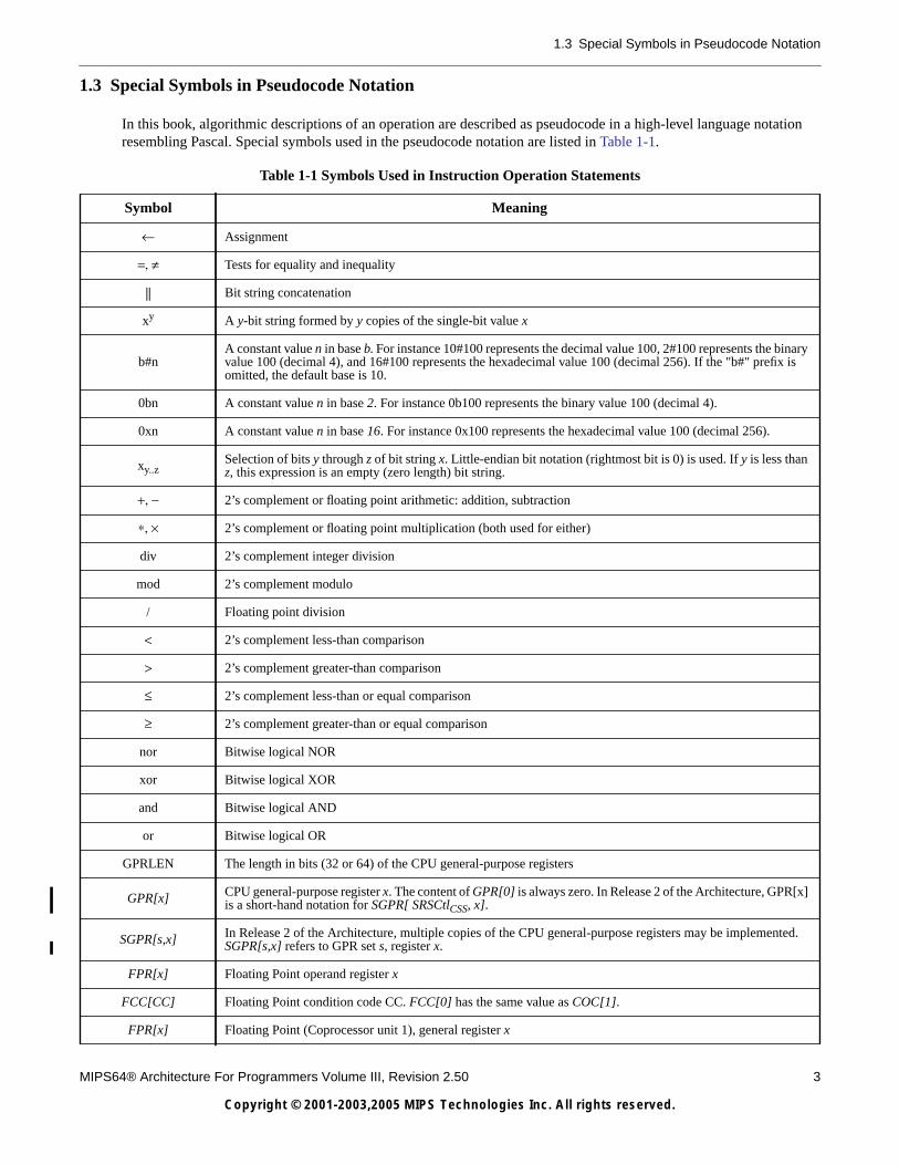
1.3 Special Symbols in Pseudocode Notation
MIPS64® Architecture For Programmers Volume III, Revision 2.50 3
Copyright © 2001-2003,2005 MIPS Technologies Inc. All rights reserved.
1.3 Special Symbols in Pseudocode Notation
In this book, algorithmic descriptions of an operation are described as pseudocode in a high-level language notationresembling Pascal. Special symbols used in the pseudocode notation are listed in Table 1-1.
Table 1-1 Symbols Used in Instruction Operation Statements
Symbol Meaning
← Assignment
=, ≠ Tests for equality and inequality
|| Bit string concatenation
xy A y-bit string formed by y copies of the single-bit value x
b#nA constant value n in base b. For instance 10#100 represents the decimal value 100, 2#100 represents the binaryvalue 100 (decimal 4), and 16#100 represents the hexadecimal value 100 (decimal 256). If the "b#" prefix isomitted, the default base is 10.
0bn A constant value n in base 2. For instance 0b100 represents the binary value 100 (decimal 4).
0xn A constant value n in base 16. For instance 0x100 represents the hexadecimal value 100 (decimal 256).
xy..zSelection of bits y through z of bit string x. Little-endian bit notation (rightmost bit is 0) is used. If y is less thanz, this expression is an empty (zero length) bit string.
+, − 2’s complement or floating point arithmetic: addition, subtraction
∗, × 2’s complement or floating point multiplication (both used for either)
div 2’s complement integer division
mod 2’s complement modulo
/ Floating point division
< 2’s complement less-than comparison
> 2’s complement greater-than comparison
≤ 2’s complement less-than or equal comparison
≥ 2’s complement greater-than or equal comparison
nor Bitwise logical NOR
xor Bitwise logical XOR
and Bitwise logical AND
or Bitwise logical OR
GPRLEN The length in bits (32 or 64) of the CPU general-purpose registers
GPR[x] CPU general-purpose register x. The content of GPR[0] is always zero. In Release 2 of the Architecture, GPR[x]is a short-hand notation for SGPR[ SRSCtlCSS, x].
SGPR[s,x] In Release 2 of the Architecture, multiple copies of the CPU general-purpose registers may be implemented.SGPR[s,x] refers to GPR set s, register x.
FPR[x] Floating Point operand register x
FCC[CC] Floating Point condition code CC. FCC[0] has the same value as COC[1].
FPR[x] Floating Point (Coprocessor unit 1), general register x
4 MIPS64® Architecture For Programmers Volume III, Revision 2.50
Copyright © 2001-2003,2005 MIPS Technologies Inc. All rights reserved.
Chapter 1 About This Book
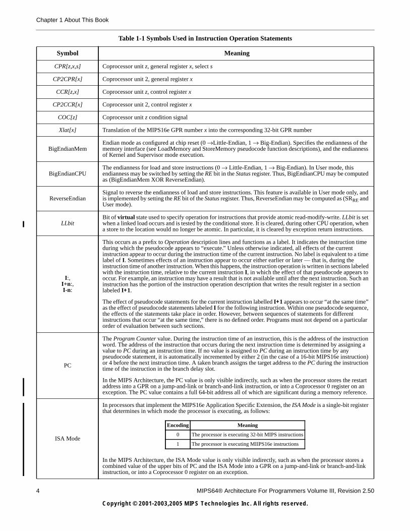
CPR[z,x,s] Coprocessor unit z, general register x, select s
CP2CPR[x] Coprocessor unit 2, general register x
CCR[z,x] Coprocessor unit z, control register x
CP2CCR[x] Coprocessor unit 2, control register x
COC[z] Coprocessor unit z condition signal
Xlat[x] Translation of the MIPS16e GPR number x into the corresponding 32-bit GPR number
BigEndianMemEndian mode as configured at chip reset (0 →Little-Endian, 1 → Big-Endian). Specifies the endianness of thememory interface (see LoadMemory and StoreMemory pseudocode function descriptions), and the endiannessof Kernel and Supervisor mode execution.
BigEndianCPUThe endianness for load and store instructions (0 → Little-Endian, 1 → Big-Endian). In User mode, thisendianness may be switched by setting the RE bit in the Status register. Thus, BigEndianCPU may be computedas (BigEndianMem XOR ReverseEndian).
ReverseEndianSignal to reverse the endianness of load and store instructions. This feature is available in User mode only, andis implemented by setting the RE bit of the Status register. Thus, ReverseEndian may be computed as (SRRE andUser mode).
LLbitBit of virtual state used to specify operation for instructions that provide atomic read-modify-write. LLbit is setwhen a linked load occurs and is tested by the conditional store. It is cleared, during other CPU operation, whena store to the location would no longer be atomic. In particular, it is cleared by exception return instructions.
I:,I+n:,I-n:
This occurs as a prefix to Operation description lines and functions as a label. It indicates the instruction timeduring which the pseudocode appears to “execute.” Unless otherwise indicated, all effects of the currentinstruction appear to occur during the instruction time of the current instruction. No label is equivalent to a timelabel of I. Sometimes effects of an instruction appear to occur either earlier or later — that is, during theinstruction time of another instruction. When this happens, the instruction operation is written in sections labeledwith the instruction time, relative to the current instruction I, in which the effect of that pseudocode appears tooccur. For example, an instruction may have a result that is not available until after the next instruction. Such aninstruction has the portion of the instruction operation description that writes the result register in a sectionlabeled I+1.
The effect of pseudocode statements for the current instruction labelled I+1 appears to occur “at the same time”as the effect of pseudocode statements labeled I for the following instruction. Within one pseudocode sequence,the effects of the statements take place in order. However, between sequences of statements for differentinstructions that occur “at the same time,” there is no defined order. Programs must not depend on a particularorder of evaluation between such sections.
PC
The Program Counter value. During the instruction time of an instruction, this is the address of the instructionword. The address of the instruction that occurs during the next instruction time is determined by assigning avalue to PC during an instruction time. If no value is assigned to PC during an instruction time by anypseudocode statement, it is automatically incremented by either 2 (in the case of a 16-bit MIPS16e instruction)or 4 before the next instruction time. A taken branch assigns the target address to the PC during the instructiontime of the instruction in the branch delay slot.
In the MIPS Architecture, the PC value is only visible indirectly, such as when the processor stores the restartaddress into a GPR on a jump-and-link or branch-and-link instruction, or into a Coprocessor 0 register on anexception. The PC value contains a full 64-bit address all of which are significant during a memory reference.
ISA Mode
In processors that implement the MIPS16e Application Specific Extension, the ISA Mode is a single-bit registerthat determines in which mode the processor is executing, as follows:
In the MIPS Architecture, the ISA Mode value is only visible indirectly, such as when the processor stores acombined value of the upper bits of PC and the ISA Mode into a GPR on a jump-and-link or branch-and-linkinstruction, or into a Coprocessor 0 register on an exception.
Table 1-1 Symbols Used in Instruction Operation Statements
Symbol Meaning
Encoding Meaning
0 The processor is executing 32-bit MIPS instructions
1 The processor is executing MIIPS16e instructions
1.4 For More Information
MIPS64® Architecture For Programmers Volume III, Revision 2.50 5
Copyright © 2001-2003,2005 MIPS Technologies Inc. All rights reserved.
1.4 For More Information
Various MIPS RISC processor manuals and additional information about MIPS products can be found at the MIPS URL:
http://www.mips.com
Comments or questions on the MIPS64® Architecture or this document should be directed to
MIPS Architecture GroupMIPS Technologies, Inc.1225 Charleston RoadMountain View, CA 94043
or via E-mail to [email protected].
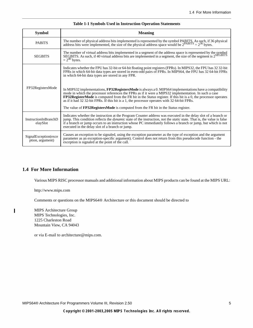
PABITS The number of physical address bits implemented is represented by the symbol PABITS. As such, if 36 physicaladdress bits were implemented, the size of the physical address space would be 2PABITS = 236 bytes.
SEGBITSThe number of virtual address bits implemented in a segment of the address space is represented by the symbolSEGBITS. As such, if 40 virtual address bits are implemented in a segment, the size of the segment is 2SEGBITS
= 240 bytes.
FP32RegistersMode
Indicates whether the FPU has 32-bit or 64-bit floating point registers (FPRs). In MIPS32, the FPU has 32 32-bitFPRs in which 64-bit data types are stored in even-odd pairs of FPRs. In MIPS64, the FPU has 32 64-bit FPRsin which 64-bit data types are stored in any FPR.
In MIPS32 implementations, FP32RegistersMode is always a 0. MIPS64 implementations have a compatibilitymode in which the processor references the FPRs as if it were a MIPS32 implementation. In such a caseFP32RegisterMode is computed from the FR bit in the Status register. If this bit is a 0, the processor operatesas if it had 32 32-bit FPRs. If this bit is a 1, the processor operates with 32 64-bit FPRs.
The value of FP32RegistersMode is computed from the FR bit in the Status register.
InstructionInBranchDelaySlot
Indicates whether the instruction at the Program Counter address was executed in the delay slot of a branch orjump. This condition reflects the dynamic state of the instruction, not the static state. That is, the value is falseif a branch or jump occurs to an instruction whose PC immediately follows a branch or jump, but which is notexecuted in the delay slot of a branch or jump.
SignalException(exception, argument)
Causes an exception to be signaled, using the exception parameter as the type of exception and the argumentparameter as an exception-specific argument). Control does not return from this pseudocode function - theexception is signaled at the point of the call.
Table 1-1 Symbols Used in Instruction Operation Statements
Symbol Meaning
6 MIPS64® Architecture For Programmers Volume III, Revision 2.50
Copyright © 2001-2003,2005 MIPS Technologies Inc. All rights reserved.
Chapter 1 About This Book
MIPS64® Architecture For Programmers Volume III, Revision 2.50 7
Copyright © 2001-2003,2005 MIPS Technologies Inc. All rights reserved.
Chapter 2
The MIPS64 Privileged Resource Architecture
2.1 Introduction
The MIPS64 Privileged Resource Architecture (PRA) is a set of environments and capabilities on which the InstructionSet Architecture operates. The effects of some components of the PRA are user-visible, for instance, the virtual memorylayout. Many other components are visible only to the operating system kernel and to systems programmers. The PRAprovides the mechanisms necessary to manage the resources of the CPU: virtual memory, caches, exceptions and usercontexts. This chapter describes these mechanisms.
2.2 The MIPS Coprocessor Model
The MIPS ISA provides for up to 4 coprocessors. A coprocessor extends the functionality of the MIPS ISA, whilesharing the instruction fetch and execution control logic of the CPU. Some coprocessors, such as the system coprocessorand the floating point unit are standard parts of the ISA, and are specified as such in the architecture documents.Coprocessors are generally optional, with one exception: CP0, the system coprocessor, is required. CP0 is the ISAinterface to the Privileged Resource Architecture and provides full control of the processor state and modes.
2.2.1 CP0 - The System Coprocessor
CP0 provides an abstraction of the functions necessary to support an operating system: exception handling, memorymanagement, scheduling, and control of critical resources. The interface to CP0 is through various instructions encodedwith the COP0 opcode, including the ability to move data to and from the CP0 registers, and specific functions thatmodify CP0 state. The CP0 registers and the interaction with them make up much of the Privileged ResourceArchitecture.
2.2.2 CP0 Registers
The CP0 registers provide the interface between the ISA and the PRA. The CP0 registers are described in Chapter 8.

8 MIPS64® Architecture For Programmers Volume III, Revision 2.50
Copyright © 2001-2003,2005 MIPS Technologies Inc. All rights reserved.
Chapter 2 The MIPS64 Privileged Resource Architecture
MIPS64® Architecture For Programmers Volume III, Revision 2.50 9
Copyright © 2001-2003,2005 MIPS Technologies Inc. All rights reserved.
Chapter 3
MIPS64 Operating Modes
The MIPS64 PRA requires two operating mode: User Mode and Kernel Mode. When operating in User Mode, theprogrammer has access to the CPU and FPU registers that are provided by the ISA and to a flat, uniform virtual memoryaddress space. When operating in Kernel Mode, the system programmer has access to the full capabilities of theprocessor, including the ability to change virtual memory mapping, control the system environment, and context switchbetween processes.
In addition, the MIPS64 PRA supports the implementation of two additional modes: Supervisor Mode and EJTAGDebug Mode. Refer to the EJTAG specification for a description of Debug Mode.
In Release 2 of the Architecture, support was added for 64-bit coprocessors (and, in particular, 64-bit floating point units)with 32-bit CPUs. As such, certain floating point instructions which were previously enabled by 64-bit operations on aMIPS64 processor are now enabled by a new 64-bit floating point operations enabled.
Finally, the MIPS64 PRA provides backward compatible support for 32-bit programs by providing enables for both64-bit addressing and 64-bit operations. If access is not enabled, an attempt to reference a 64-bit address or an instructionthat implements a 64-bit operation results in an exception.
3.1 Debug Mode
For processors that implement EJTAG, the processor is operating in Debug Mode if the DM bit in the CP0 Debug registeris a one. If the processor is running in Debug Mode, it has full access to all resources that are available to Kernel Modeoperation.
3.2 Kernel Mode
The processor is operating in Kernel Mode when the DM bit in the Debug register is a zero (if the processor implementsDebug Mode), and any of the following three conditions is true:
• The KSU field in the CP0 Status register contains 0b00
• The EXL bit in the Status register is one
• The ERL bit in the Status register is one
The processor enters Kernel Mode at power-up, or as the result of an interrupt, exception, or error. The processor leavesKernel Mode and enters User Mode or Supervisor Mode when all of the previous three conditions are false, usually asthe result of an ERET instruction.
3.3 Supervisor Mode
The processor is operating in Supervisor Mode (if that optional mode is implemented by the processor) when all of thefollowing conditions are true:
• The DM bit in the Debug register is a zero (if the processor implements Debug Mode)
• The KSU field in the Status register contains 0b01

10 MIPS64® Architecture For Programmers Volume III, Revision 2.50
Copyright © 2001-2003,2005 MIPS Technologies Inc. All rights reserved.
Chapter 3 MIPS64 Operating Modes
• The EXL and ERL bits in the Status register are both zero
3.4 User Mode
The processor is operating in User Mode when all of the following conditions are true:
• The DM bit in the Debug register is a zero (if the processor implements Debug Mode)
• The KSU field in the Status register contains 0b10
• The EXL and ERL bits in the Status register are both zero
3.5 Other Modes
3.5.1 64-bit Address Enable
Access to 64-bit addresses are enabled under any of the following conditions:
• A legal reference to a kernel address space occurs and the KX bit in the Status register is a one
• A legal reference to a supervisor address space occurs and the SX bit in the Status register is a one
• A legal reference to a user address space occurs and the UX bit in the Status register is a one
Note that the operating mode of the processor is not relevant to 64-bit address enables. That is, a reference to user addressspace made while the processor is operating in Kernel Mode is controlled by the state of the UX bit, not by the KX bit.
An attempt to reference a 64-bit address space when 64-bit addresses are not enabled results in an Address ErrorException (either AdEL or AdES, depending on the type of reference).
When a TLB miss occurs, the choice of the Exception Vector is also determined by the 64-bit address enable. If 64-bitaddresses are not enabled for the reference, the TLB Refill Vector is used. If 64-bit addresses are enabled for thereference, the XTLB Refill Vector is used.
3.5.2 64-bit Operations Enable
Instructions that perform 64-bit operations are legal under any of the following conditions:
• The processor is operating in Kernel Mode, Supervisor Mode, or Debug Mode, as described above.
• The PX bit in the Status register is a one
• The processor is operating in User Mode, as described above, and the UX bit in the Status register is a one.
The last two bullets imply that 64-bit operations are legal in User Mode when either the PX bit or the UX bit is a one inthe Status register.
An attempt to execute an instruction which performs 64-bit operations when such instructions are not enabled results ina Reserved Instruction Exception.
3.5.3 64-bit Floating Point Operations Enable
Instructions that are implemented by a 64-bit floating point unit are legal under any of the following conditions:
3.5 Other Modes
MIPS64® Architecture For Programmers Volume III, Revision 2.50 11
Copyright © 2001-2003,2005 MIPS Technologies Inc. All rights reserved.
• In an implementation of Release 1 of the Architecture, 64-bit floating point operations are enabled only if 64-bitoperations enabled.
• If an implementation of Release 2 of the Architecture, 64-bit floating point operations are enabled if the F64 bit in theFIR register is a one. The processor must also implement the floating point data type.
3.5.4 64-bit FPR Enable
Access to 64-bit FPRs is controlled by the FR bit in the Status register. If the FR bit is one, the FPRs are interpreted as32 64-bit registers that may contain any data type. If the FR bit is zero, the FPRs are interpreted as 32 32-bit registers,any of which may contain a 32-bit data type (W, S). In this case, 64-bit data types are contained in even-odd pairs ofregisters.
64-bit FPRs are supported in a MIPS64 processor in Release 1 of the Architecture, or in a 64-bit floating point unit, forboth MIPS32 and MIPS64 processors, in Release 2 of the Architecture.
The operation of the processor is UNPREDICTABLE under the following conditions:
• The FR bit is a zero, 64-bit operations are enabled, and a floating point instruction is executed whose datatype is L orPS.
• The FR bit is a zero and an odd register is referenced by an instruction whose datatype is 64-bits
3.5.5 Coprocessor 0 Enable
Access to Coprocessor 0 registers are enabled under any of the following conditions:
• The processor is running in Kernel Mode or Debug Mode, as defined above
• The CU0 bit in the Status register is one.

12 MIPS64® Architecture For Programmers Volume III, Revision 2.50
Copyright © 2001-2003,2005 MIPS Technologies Inc. All rights reserved.
Chapter 3 MIPS64 Operating Modes

MIPS64® Architecture For Programmers Volume III, Revision 2.50 13
Copyright © 2001-2003,2005 MIPS Technologies Inc. All rights reserved.
Chapter 4
Virtual Memory
4.1 Support in Release 1 and Release 2 of the Architecture
4.1.1 Virtual Memory
In Release 1 of the Architecture, the minimum page size was 4KB, with optional support for pages as large as 256MB.In Release 2 of the Architecture, optional support for 1KB pages was added for use in specific embedded applicationsthat require access to pages smaller than 4KB. Such usage is expected to be in conjunction with a default page size of4KB and is not intended or suggested to replace the default 4KB page size but, rather, to augment it.
Support for 1KB pages involves the following changes:
• Addition of the PageGrain register. This register is also used by the SmartMIPS™ ASE specification, but bits usedby Release 2 of the Architecture and the SmartMIPS ASE specification do not overlap.
• Modification of the EntryHi register to enable writes to, and use of, bits 12..11 (VPN2X).
• Modification of the PageMask register to enable writes to, and use of, bits 12..11 (MaskX).
• Modification of the EntryLo0 and EntryLo1 registers to shift the PFN field to the left by 2 bits, when 1KB pagesupport is enabled, to create space for two lower-order physical address bits.
Support for 1KB pages is denoted by the Config3SP bit and enabled by the PageGrainESP bit.
4.1.2 Physical Memory
In Release 1 of the Architecture, the physical address size was limited by the format of the EntryLo0 and EntryLo1registers to 36 bits. Some applications of MIPS processors already require more than 36 bits of physical address (forexample, high-end networking), and others are expected to appear during the lifetime of Release 2 of the architecture.As such, Release 2 adds an optional extension to the architecture to provide up to 59 bits of physical address for MIPS64processors. This extension is optional because several operating systems currently use the reserved bits to the left of thePFN field in the EntryLo0 and EntryLo1 registers for PTE software flags. The flags are loaded directly into these registerson a TLB Refill exception. As such, for compatibility with existing software, the extension of the PFN field must be donewith an explicit enable.
Support for extended PFNs is denoted by the Config3LPA bit and enabled by the PageGrainELPA bit.
4.2 Terminology
4.2.1 Address Space
An Address Space is the range of all possible addresses that can be generated for a particular addressing mode. There isone 64-bit Address Space and one 32-bit Compatibility Address Space that is mapped into a subset of the 64-bit AddressSpace.
14 MIPS64® Architecture For Programmers Volume III, Revision 2.50
Copyright © 2001-2003,2005 MIPS Technologies Inc. All rights reserved.
Chapter 4 Virtual Memory
4.2.2 Segment and Segment Size (SEGBITS)
A Segment is a defined subset of an Address Space that has self-consistent reference and access behavior. A 32-bitCompatibility Segment is part of the 32-bit Compatibility Address Space and is either 229 or 231 bytes in size, dependingon the specific Segment. A 64-bit Segment is part of the 64-bit Address Space and is no larger than 262 bytes in size, butmay be smaller on an implementation dependent basis. The symbol SEGBITS is used to represent the actual number ofbits implemented in each 64-bit Segment. As such, if 40 virtual address bits were implemented, the actual size of theSegment would be 2SEGBITS = 240 bytes. Software may determine the value of SEGBITS by writing all ones to theEntryHi register and reading the value back. Bits read as “1” from the VPN2 field allow software to determine theboundary between the VPN2 and Fill fields to calculate the value of SEGBITS.
4.2.3 Physical Address Size (PABITS)
The number of physical address bits implemented is represented by the symbol PABITS. As such, if 36 physical addressbits were implemented, the size of the physical address space would be 2PABITS = 236 bytes. The format of the EntryLo0and EntryLo1 registers implicitly limits the physical address size to 236 bytes. Software may determine the value ofPABITS by writing all ones to the EntryLo0 or EntryLo1 registers and reading the value back. Bits read as “1” from thePFN field allow software to determine the boundary between the PFN and Fill fields to calculate the value of PABITS.
4.3 Virtual Address Spaces
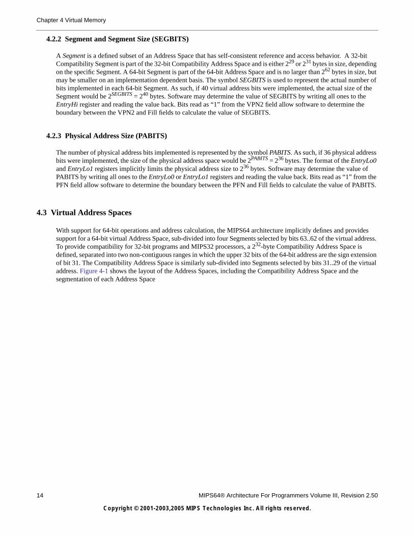
With support for 64-bit operations and address calculation, the MIPS64 architecture implicitly defines and providessupport for a 64-bit virtual Address Space, sub-divided into four Segments selected by bits 63..62 of the virtual address.To provide compatibility for 32-bit programs and MIPS32 processors, a 232-byte Compatibility Address Space isdefined, separated into two non-contiguous ranges in which the upper 32 bits of the 64-bit address are the sign extensionof bit 31. The Compatibility Address Space is similarly sub-divided into Segments selected by bits 31..29 of the virtualaddress. Figure 4-1 shows the layout of the Address Spaces, including the Compatibility Address Space and thesegmentation of each Address Space
4.3 Virtual Address Spaces
MIPS64® Architecture For Programmers Volume III, Revision 2.50 15
Copyright © 2001-2003,2005 MIPS Technologies Inc. All rights reserved.
.
Each Segment of an Address Space is classified as “Mapped” or “Unmapped”. A “Mapped” address is one that istranslated through the TLB or other address translation unit. An “Unmapped” address is one which is not translatedthrough the TLB and which provides a window into the lowest portion of the physical address space, starting at physicaladdress zero, and with a size corresponding to the size of the unmapped Segment.
Additionally, the kseg1 Segment is classified as “Uncached”. References to this Segment bypass all levels of the cachehierarchy and allow direct access to memory without any interference from the caches.
Table 4-1 lists the same information in tabular form.
Figure 4-1 Virtual Address Spaces
64-bit Virtual Memory Address Space 32-bit Compatibility Address Space
0xFFFF FFFF FFFF FFFF
Kernel Mapped
0xFFFF FFFF FFFF FFFF
Kernel Mapped
kseg3
0xFFFF FFFF E000 0000
xkseg
Supervisor Mapped
0xFFFF FFFF DFFF FFFF
sseg
0xFFFF FFFF C000 0000
0xC000 0000 0000 0000Kernel Unmapped
Uncached
0xFFFF FFFF BFFF FFFF
0xBFFF FFFF FFFF FFFF
Kernel Unmapped
kseg1
0xFFFF FFFF A000 0000
Kernel Unmapped
0xFFFF FFFF 9FFF FFFF
xkphys kseg0
0xFFFF FFFF 8000 0000
0x8000 0000 0000 0000
0x7FFF FFFF FFFF FFFF
Supervisor Mapped
User Mapped
0x0000 0000 7FFF FFFF
xsseg
0x4000 0000 0000 0000
0x3FFF FFFF FFFF FFFF
User Mapped
useg
xuseg
0x0000 0000 0000 0000 0x0000 0000 0000 0000
231
-byt
e C
ompa
tibili
ty S
egm
ent
2 31-byte Com
patibility Segment
16 MIPS64® Architecture For Programmers Volume III, Revision 2.50
Copyright © 2001-2003,2005 MIPS Technologies Inc. All rights reserved.
Chapter 4 Virtual Memory
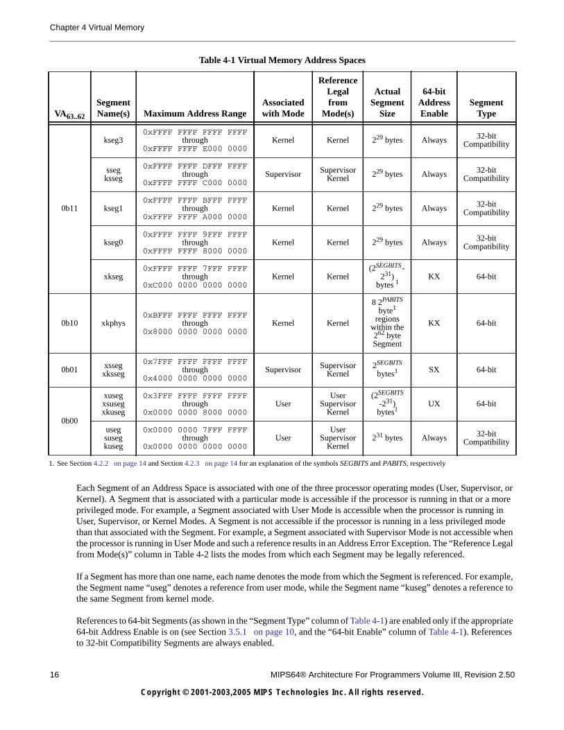
Each Segment of an Address Space is associated with one of the three processor operating modes (User, Supervisor, orKernel). A Segment that is associated with a particular mode is accessible if the processor is running in that or a moreprivileged mode. For example, a Segment associated with User Mode is accessible when the processor is running inUser, Supervisor, or Kernel Modes. A Segment is not accessible if the processor is running in a less privileged modethan that associated with the Segment. For example, a Segment associated with Supervisor Mode is not accessible whenthe processor is running in User Mode and such a reference results in an Address Error Exception. The “Reference Legalfrom Mode(s)” column in Table 4-2 lists the modes from which each Segment may be legally referenced.
If a Segment has more than one name, each name denotes the mode from which the Segment is referenced. For example,the Segment name “useg” denotes a reference from user mode, while the Segment name “kuseg” denotes a reference tothe same Segment from kernel mode.
References to 64-bit Segments (as shown in the “Segment Type” column of Table 4-1) are enabled only if the appropriate64-bit Address Enable is on (see Section 3.5.1 on page 10, and the “64-bit Enable” column of Table 4-1). Referencesto 32-bit Compatibility Segments are always enabled.
Table 4-1 Virtual Memory Address Spaces
VA63..62
SegmentName(s) Maximum Address Range
Associatedwith Mode
ReferenceLegalfrom
Mode(s)
ActualSegment
Size
64-bitAddressEnable
SegmentType
0b11
kseg30xFFFF FFFF FFFF FFFF
through0xFFFF FFFF E000 0000
Kernel Kernel 229 bytes Always 32-bitCompatibility
ssegksseg
0xFFFF FFFF DFFF FFFFthrough
0xFFFF FFFF C000 0000Supervisor Supervisor
Kernel 229 bytes Always 32-bitCompatibility
kseg10xFFFF FFFF BFFF FFFF
through0xFFFF FFFF A000 0000
Kernel Kernel 229 bytes Always 32-bitCompatibility
kseg00xFFFF FFFF 9FFF FFFF
through0xFFFF FFFF 8000 0000
Kernel Kernel 229 bytes Always 32-bitCompatibility
xkseg0xFFFF FFFF 7FFF FFFF
through0xC000 0000 0000 0000
Kernel Kernel(2SEGBITS-
231)bytes 1
KX 64-bit
0b10 xkphys0xBFFF FFFF FFFF FFFF
through0x8000 0000 0000 0000
Kernel Kernel
8 2PABITS
byte1
regionswithin the262 byteSegment
KX 64-bit
0b01 xssegxksseg
0x7FFF FFFF FFFF FFFFthrough
0x4000 0000 0000 0000Supervisor Supervisor
Kernel2SEGBITS
bytes1 SX 64-bit
0b00
xusegxsusegxkuseg
0x3FFF FFFF FFFF FFFFthrough
0x0000 0000 8000 0000User
UserSupervisor
Kernel
(2SEGBITS
-231)bytes1
1. See Section 4.2.2 on page 14 and Section 4.2.3 on page 14 for an explanation of the symbols SEGBITS and PABITS, respectively
UX 64-bit
usegsusegkuseg
0x0000 0000 7FFF FFFFthrough
0x0000 0000 0000 0000User
UserSupervisor
Kernel231 bytes Always 32-bit
Compatibility
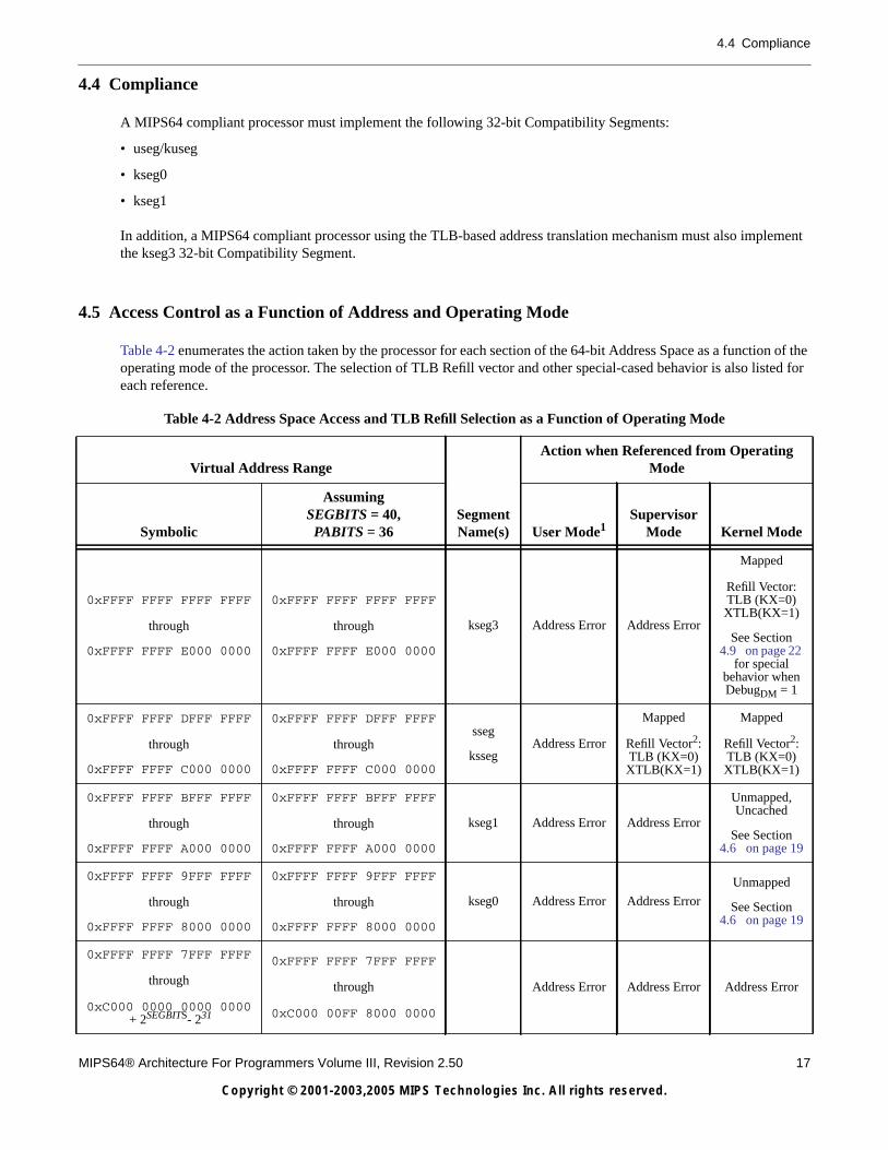
4.4 Compliance
MIPS64® Architecture For Programmers Volume III, Revision 2.50 17
Copyright © 2001-2003,2005 MIPS Technologies Inc. All rights reserved.
4.4 Compliance
A MIPS64 compliant processor must implement the following 32-bit Compatibility Segments:
• useg/kuseg
• kseg0
• kseg1
In addition, a MIPS64 compliant processor using the TLB-based address translation mechanism must also implementthe kseg3 32-bit Compatibility Segment.
4.5 Access Control as a Function of Address and Operating Mode
Table 4-2 enumerates the action taken by the processor for each section of the 64-bit Address Space as a function of theoperating mode of the processor. The selection of TLB Refill vector and other special-cased behavior is also listed foreach reference.
Table 4-2 Address Space Access and TLB Refill Selection as a Function of Operating Mode
Virtual Address Range
SegmentName(s)
Action when Referenced from OperatingMode
Symbolic
AssumingSEGBITS = 40,PABITS = 36 User Mode1
SupervisorMode Kernel Mode
0xFFFF FFFF FFFF FFFF
through
0xFFFF FFFF E000 0000
0xFFFF FFFF FFFF FFFF
through
0xFFFF FFFF E000 0000
kseg3 Address Error Address Error
Mapped
Refill Vector:TLB (KX=0)XTLB(KX=1)
See Section4.9 on page 22
for specialbehavior whenDebugDM = 1
0xFFFF FFFF DFFF FFFF
through
0xFFFF FFFF C000 0000
0xFFFF FFFF DFFF FFFF
through
0xFFFF FFFF C000 0000
sseg
kssegAddress Error
Mapped
Refill Vector2:TLB (KX=0)XTLB(KX=1)
Mapped
Refill Vector2:TLB (KX=0)XTLB(KX=1)
0xFFFF FFFF BFFF FFFF
through
0xFFFF FFFF A000 0000
0xFFFF FFFF BFFF FFFF
through
0xFFFF FFFF A000 0000
kseg1 Address Error Address Error
Unmapped,Uncached
See Section4.6 on page 19
0xFFFF FFFF 9FFF FFFF
through
0xFFFF FFFF 8000 0000
0xFFFF FFFF 9FFF FFFF
through
0xFFFF FFFF 8000 0000
kseg0 Address Error Address Error
Unmapped
See Section4.6 on page 19
0xFFFF FFFF 7FFF FFFF
through
0xC000 0000 0000 0000 + 2SEGBITS- 231
0xFFFF FFFF 7FFF FFFF
through
0xC000 00FF 8000 0000
Address Error Address Error Address Error
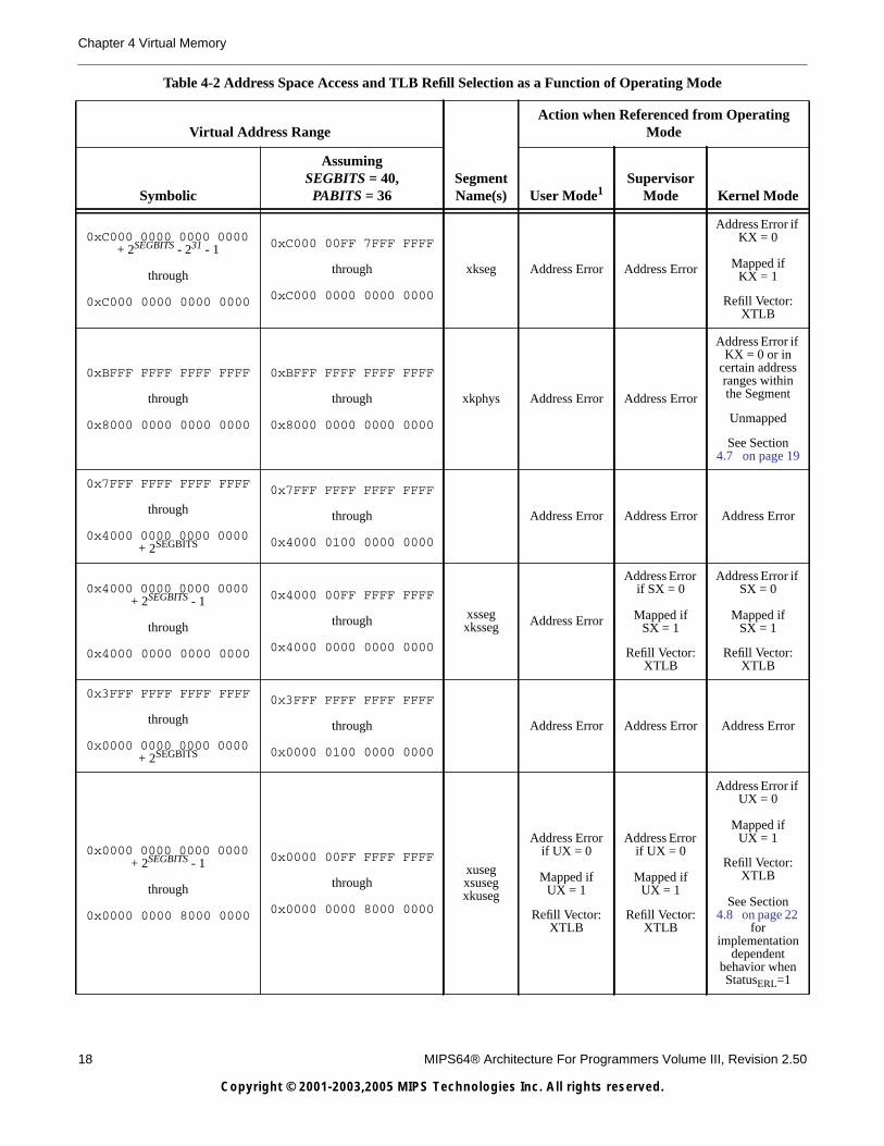
18 MIPS64® Architecture For Programmers Volume III, Revision 2.50
Copyright © 2001-2003,2005 MIPS Technologies Inc. All rights reserved.
Chapter 4 Virtual Memory
0xC000 0000 0000 0000+ 2SEGBITS - 231 - 1
through
0xC000 0000 0000 0000
0xC000 00FF 7FFF FFFF
through
0xC000 0000 0000 0000
xkseg Address Error Address Error
Address Error ifKX = 0
Mapped ifKX = 1
Refill Vector:XTLB
0xBFFF FFFF FFFF FFFF
through
0x8000 0000 0000 0000
0xBFFF FFFF FFFF FFFF
through
0x8000 0000 0000 0000
xkphys Address Error Address Error
Address Error ifKX = 0 or in
certain addressranges withinthe Segment
Unmapped
See Section4.7 on page 19
0x7FFF FFFF FFFF FFFF
through
0x4000 0000 0000 0000+ 2SEGBITS
0x7FFF FFFF FFFF FFFF
through
0x4000 0100 0000 0000
Address Error Address Error Address Error
0x4000 0000 0000 0000+ 2SEGBITS - 1
through
0x4000 0000 0000 0000
0x4000 00FF FFFF FFFF
through
0x4000 0000 0000 0000
xssegxksseg Address Error
Address Errorif SX = 0
Mapped ifSX = 1
Refill Vector:XTLB
Address Error ifSX = 0
Mapped ifSX = 1
Refill Vector:XTLB
0x3FFF FFFF FFFF FFFF
through
0x0000 0000 0000 0000+ 2SEGBITS
0x3FFF FFFF FFFF FFFF
through
0x0000 0100 0000 0000
Address Error Address Error Address Error
0x0000 0000 0000 0000+ 2SEGBITS - 1
through
0x0000 0000 8000 0000
0x0000 00FF FFFF FFFF
through
0x0000 0000 8000 0000
xusegxsusegxkuseg
Address Errorif UX = 0
Mapped ifUX = 1
Refill Vector:XTLB
Address Errorif UX = 0
Mapped ifUX = 1
Refill Vector:XTLB
Address Error ifUX = 0
Mapped ifUX = 1
Refill Vector:XTLB
See Section4.8 on page 22
forimplementation
dependentbehavior whenStatusERL=1
Table 4-2 Address Space Access and TLB Refill Selection as a Function of Operating Mode
Virtual Address Range
SegmentName(s)
Action when Referenced from OperatingMode
Symbolic
AssumingSEGBITS = 40,PABITS = 36 User Mode1
SupervisorMode Kernel Mode
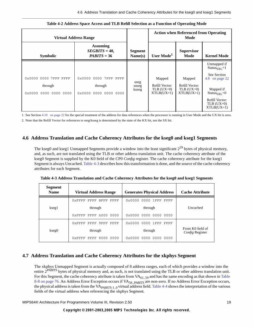
4.6 Address Translation and Cache Coherency Attributes for the kseg0 and kseg1 Segments
MIPS64® Architecture For Programmers Volume III, Revision 2.50 19
Copyright © 2001-2003,2005 MIPS Technologies Inc. All rights reserved.
4.6 Address Translation and Cache Coherency Attributes for the kseg0 and kseg1 Segments
The kseg0 and kseg1 Unmapped Segments provide a window into the least significant 229 bytes of physical memory,and, as such, are not translated using the TLB or other address translation unit. The cache coherency attribute of thekseg0 Segment is supplied by the K0 field of the CP0 Config register. The cache coherency attribute for the kseg1Segment is always Uncached. Table 4-3 describes how this transformation is done, and the source of the cache coherencyattributes for each Segment.
4.7 Address Translation and Cache Coherency Attributes for the xkphys Segment
The xkphys Unmapped Segment is actually composed of 8 address ranges, each of which provides a window into theentire 2PABITS bytes of physical memory and, as such, is not translated using the TLB or other address translation unit.For this Segment, the cache coherency attribute is taken from VA61..59 and has the same encoding as that shown in Table8-8 on page 76. An Address Error Exception occurs if VA58..PABITS are non-zero. If no Address Error Exception occurs,the physical address is taken from the VAPABITS-1..0 virtual address field. Table 4-4 shows the interpretation of the variousfields of the virtual address when referencing the xkphys Segment.
0x0000 0000 7FFF FFFF
through
0x0000 0000 0000 0000
0x0000 0000 7FFF FFFF
through
0x0000 0000 0000 0000
usegsusegkuseg
Mapped
Refill Vector:TLB (UX=0)XTLB(UX=1)
Mapped
Refill Vector:TLB (UX=0)XTLB(UX=1)
Unmapped ifStatusERL=1
See Section4.8 on page 22
Mapped ifStatusERL=0
Refill Vector:TLB (UX=0)XTLB(UX=1)
1. See Section 4.10 on page 22 for the special treatment of the address for data references when the processor is running in User Mode and the UX bit is zero.
2. Note that the Refill Vector for references to sseg/ksseg is determined by the state of the KX bit, not the SX bit.
Table 4-3 Address Translation and Cache Coherency Attributes for the kseg0 and kseg1 Segments
SegmentName Virtual Address Range Generates Physical Address Cache Attribute
kseg1
0xFFFF FFFF BFFF FFFF
through
0xFFFF FFFF A000 0000
0x0000 0000 1FFF FFFF
through
0x0000 0000 0000 0000
Uncached
kseg0
0xFFFF FFFF 9FFF FFFF
through
0xFFFF FFFF 8000 0000
0x0000 0000 1FFF FFFF
through
0x0000 0000 0000 0000
From K0 field ofConfig Register
Table 4-2 Address Space Access and TLB Refill Selection as a Function of Operating Mode
Virtual Address Range
SegmentName(s)
Action when Referenced from OperatingMode
Symbolic
AssumingSEGBITS = 40,PABITS = 36 User Mode1
SupervisorMode Kernel Mode
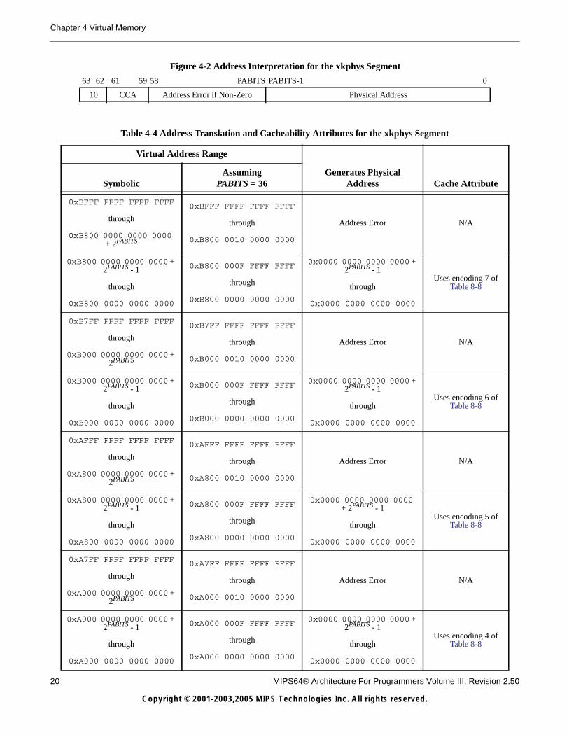
20 MIPS64® Architecture For Programmers Volume III, Revision 2.50
Copyright © 2001-2003,2005 MIPS Technologies Inc. All rights reserved.
Chapter 4 Virtual Memory
Figure 4-2 Address Interpretation for the xkphys Segment
63 62 61 59 58 PABITS PABITS-1 0
10 CCA Address Error if Non-Zero Physical Address
Table 4-4 Address Translation and Cacheability Attributes for the xkphys Segment
Virtual Address Range
Generates PhysicalAddress Cache AttributeSymbolic
AssumingPABITS = 36
0xBFFF FFFF FFFF FFFF
through
0xB800 0000 0000 0000+ 2PABITS
0xBFFF FFFF FFFF FFFF
through
0xB800 0010 0000 0000
Address Error N/A
0xB800 0000 0000 0000 +2PABITS - 1
through
0xB800 0000 0000 0000
0xB800 000F FFFF FFFF
through
0xB800 0000 0000 0000
0x0000 0000 0000 0000 +2PABITS - 1
through
0x0000 0000 0000 0000
Uses encoding 7 ofTable 8-8
0xB7FF FFFF FFFF FFFF
through
0xB000 0000 0000 0000 +2PABITS
0xB7FF FFFF FFFF FFFF
through
0xB000 0010 0000 0000
Address Error N/A
0xB000 0000 0000 0000 +2PABITS - 1
through
0xB000 0000 0000 0000
0xB000 000F FFFF FFFF
through
0xB000 0000 0000 0000
0x0000 0000 0000 0000 +2PABITS - 1
through
0x0000 0000 0000 0000
Uses encoding 6 ofTable 8-8
0xAFFF FFFF FFFF FFFF
through
0xA800 0000 0000 0000 +2PABITS
0xAFFF FFFF FFFF FFFF
through
0xA800 0010 0000 0000
Address Error N/A
0xA800 0000 0000 0000 +2PABITS - 1
through
0xA800 0000 0000 0000
0xA800 000F FFFF FFFF
through
0xA800 0000 0000 0000
0x0000 0000 0000 0000+ 2PABITS - 1
through
0x0000 0000 0000 0000
Uses encoding 5 ofTable 8-8
0xA7FF FFFF FFFF FFFF
through
0xA000 0000 0000 0000 +2PABITS
0xA7FF FFFF FFFF FFFF
through
0xA000 0010 0000 0000
Address Error N/A
0xA000 0000 0000 0000 +2PABITS - 1
through
0xA000 0000 0000 0000
0xA000 000F FFFF FFFF
through
0xA000 0000 0000 0000
0x0000 0000 0000 0000 +2PABITS - 1
through
0x0000 0000 0000 0000
Uses encoding 4 ofTable 8-8
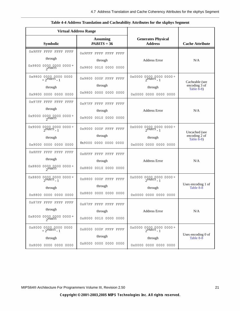
4.7 Address Translation and Cache Coherency Attributes for the xkphys Segment
MIPS64® Architecture For Programmers Volume III, Revision 2.50 21
Copyright © 2001-2003,2005 MIPS Technologies Inc. All rights reserved.
0x9FFF FFFF FFFF FFFF
through
0x9800 0000 0000 0000 +2PABITS
0x9FFF FFFF FFFF FFFF
through
0x9800 0010 0000 0000
Address Error N/A
0x9800 0000 0000 0000+ 2PABITS - 1
through
0x9800 0000 0000 0000
0x9800 000F FFFF FFFF
through
0x9800 0000 0000 0000
0x0000 0000 0000 0000 +2PABITS - 1
through
0x0000 0000 0000 0000
Cacheable (seeencoding 3 of
Table 8-8)
0x97FF FFFF FFFF FFFF
through
0x9000 0000 0000 0000 +2PABITS
0x97FF FFFF FFFF FFFF
through
0x9000 0010 0000 0000
Address Error N/A
0x9000 0000 0000 0000 +2PABITS - 1
through
0x9000 0000 0000 0000
0x9000 000F FFFF FFFF
through
0x9000 0000 0000 0000
0x0000 0000 0000 0000 +2PABITS - 1
through
0x0000 0000 0000 0000
Uncached (seeencoding 2 of
Table 8-8)
0x8FFF FFFF FFFF FFFF
through
0x8800 0000 0000 0000 +2PABITS
0x8FFF FFFF FFFF FFFF
through
0x8800 0010 0000 0000
Address Error N/A
0x8800 0000 0000 0000 +2PABITS - 1
through
0x8800 0000 0000 0000
0x8800 000F FFFF FFFF
through
0x8800 0000 0000 0000
0x0000 0000 0000 0000 +2PABITS - 1
through
0x0000 0000 0000 0000
Uses encoding 1 ofTable 8-8
0x87FF FFFF FFFF FFFF
through
0x8000 0000 0000 0000 +2PABITS
0x87FF FFFF FFFF FFFF
through
0x8000 0010 0000 0000
Address Error N/A
0x8000 0000 0000 0000+ 2PABITS - 1
through
0x8000 0000 0000 0000
0x8000 000F FFFF FFFF
through
0x8000 0000 0000 0000
0x0000 0000 0000 0000 +2PABITS - 1
through
0x0000 0000 0000 0000
Uses encoding 0 ofTable 8-8
Table 4-4 Address Translation and Cacheability Attributes for the xkphys Segment
Virtual Address Range
Generates PhysicalAddress Cache AttributeSymbolic
AssumingPABITS = 36
22 MIPS64® Architecture For Programmers Volume III, Revision 2.50
Copyright © 2001-2003,2005 MIPS Technologies Inc. All rights reserved.
Chapter 4 Virtual Memory
4.8 Address Translation for the kuseg Segment when StatusERL = 1
To provide support for the cache error handler, the kuseg Segment becomes an unmapped, uncached Segment, similarto the kseg1 Segment, if the ERL bit is set in the Status register. This allows the cache error exception code to operateuncached using GPR R0 as a base register to save other GPRs before use.
4.9 Special Behavior for the kseg3 Segment when DebugDM = 1
If EJTAG is implemented on the processor, the EJTAG block must treat the virtual address range0xFFFF FFFF FF20 0000 through 0xFFFF FFFF FF3F FFFF, inclusive, as a special memory-mapped regionin Debug Mode. A MIPS64 compliant implementation that also implements EJTAG must:
• explicitly range check the address range as given and not assume that the entire region between 0xFFFF FFFFFF20 0000 and 0xFFFF FFFF FFFF FFFF is included in the special memory-mapped region.
• not enable the special EJTAG mapping for this region in any mode other than in EJTAG Debug mode.
Even in Debug mode, normal memory rules may apply in some cases. Refer to the EJTAG specification for details onthis mapping.
4.10 Special Behavior for Data References in User Mode with StatusUX = 0
When the processor is running in User Mode, legal addresses have VA31 equal zero, and the 32-bit virtual address issign-extended (really zero-extended because VA31 is zero) into a full 64-bit address. As such, one would expect that thenormal address bounds checks on the sign-extended 64-bit address would be sufficient. Unfortunately, there are casesin which a program running on a 32-bit processor can generate a data address that is legal in 32 bits, but which is notappropriately sign-extended into 64-bits. For example, consider the following code example:
la r10, 0x80000000lw r10, -4(r10)
The results of executing this address calculation on 32-bit and 64-bit processors with UX equal zero is shown below:
On a 32-bit processor, the result of this address calculation results in a valid, useg address. On a 64-bit processor,however, the sign-extended address in the base register is added to the sign-extended displacement as a 64-bit quantitywhich results in a carry-out of bit 31, producing an address that is not properly sign extended.
To provide backward compatibility with 32-bit User Mode code, MIPS64 compliant processors must implement thefollowing special case for data references (and explicitly not for instruction references) when the processor is runningin User Mode and the UX bit is zero in the Status register:
The effective address calculated by a load, store, or prefetch instruction must be sign extended from bit 31 into bits 63..32of the full 64-bit address, ignoring the previous contents of bits 63..32 of the address, before the final address is checkedfor address error exceptions or used to access the TLB or cache. This special-case behavior is not performed forinstruction references.
32-bit Processor 64-bit Processor
0x8000 0000 0xFFFF FFFF 8000 0000
+0xFFFF FFFC +0xFFFF FFFF FFFF FFFC
0x7FFF FFFC 0xFFFF FFFF 7FFF FFFC
4.11 TLB-Based Virtual Address Translation
MIPS64® Architecture For Programmers Volume III, Revision 2.50 23
Copyright © 2001-2003,2005 MIPS Technologies Inc. All rights reserved.
This results in a properly zero-extended address for all legal data addresses (which cleans up the address shown in theexample above), and results in a properly sign-extended address for all illegal data addresses (those in which bit 31 is aone). Code running in Debug Mode, Kernel Mode, or Supervisor Mode with the appropriate 64-bit address enable off isprohibited from generating an effective address in which there is a carry-out of bit 31. If such an address is produced,the operation of the instruction generating such an address is UNPREDICTABLE.
4.11 TLB-Based Virtual Address Translation1
This section describes the TLB-based virtual address translation mechanism. Note that sufficient TLB entries must beimplemented to avoid a TLB exception loop on load and store instructions.
4.11.1 Address Space Identifiers (ASID)
The TLB-based translation mechanism supports Address Space Identifiers to uniquely identify the same virtual addressacross different processes. The operating system assigns ASIDs to each process and the TLB keeps track of the ASIDwhen doing address translation. In certain circumstances, the operating system may wish to associate the same virtualaddress with all processes. To address this need, the TLB includes a global (G) bit which over-rides the ASIDcomparison during translation.
4.11.2 TLB Organization
The TLB is a fully-associative structure which is used to translate virtual addresses. Each entry contains two logicalcomponents: a comparison section and a physical translation section. The comparison section includes the mappingregion specifier (R) and the virtual page number (VPN2 and, in Release 2, VPNX) (actually, the virtual page number/2since each entry maps two physical pages) of the entry, the ASID, the G(lobal) bit and a recommended mask field whichprovides the ability to map different page sizes with a single entry. The physical translation section contains a pair ofentries, each of which contains the physical page frame number (PFN, and in Release 2, PFNX), a valid (V) bit, a dirty(D) bit, and a cache coherency field (C), whose valid encodings are given in Table 8-8 on page 76. There are two entriesin the translation section for each TLB entry because each TLB entry maps an aligned pair of virtual pages and the pairof physical translation entries corresponds to the even and odd pages of the pair.
Figure 4-3 shows the logical arrangement of a TLB entry, including the optional support added in Release 2 of theArchitecture for 1KB page sizes and the increase in physical address size from the 36-bit limit in Release 1. Light greyfields denote extensions to the right that are required to support 1KB page sizes. Medium grey fields denote extensionsto the left that are required to support larger physical addresses. Neither set of extensions is present in an implementationof Release 1 of the Architecture.
1 Refer to Section A.1, "Fixed Mapping MMU" on page 149 and Section A.2, "Block Address Translation" on page 153 for descriptionsof alternative MMU organizations
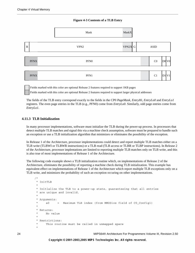
24 MIPS64® Architecture For Programmers Volume III, Revision 2.50
Copyright © 2001-2003,2005 MIPS Technologies Inc. All rights reserved.
Chapter 4 Virtual Memory
The fields of the TLB entry correspond exactly to the fields in the CP0 PageMask, EntryHi, EntryLo0 and EntryLo1registers. The even page entries in the TLB (e.g., PFN0) come from EntryLo0. Similarly, odd page entries come fromEntryLo1.
4.11.3 TLB Initialization
In many processor implementations, software must initialize the TLB during the power-up process. In processors thatdetect multiple TLB matches and signal this via a machine check assumption, software must be prepared to handle suchan exception or use a TLB initialization algorithm that minimizes or eliminates the possibility of the exception.
In Release 1 of the Architecture, processor implementations could detect and report multiple TLB matches either on aTLB write (TLBWI or TLBWR instructions) or a TLB read (TLB access or TLBR or TLBP instructions). In Release 2of the Architecture, processor implentations are limited to reporting multiple TLB matches only on TLB write, and thisis also true of most implementations of Release 1 of the Architecture.
The following code example shows a TLB initialization routine which, on implementations of Release 2 of theArchitecture, eliminates the possibility of reporting a machine check during TLB initialization. This example hasequivalent effect on implementations of Release 1 of the Architecture which report multiple TLB exceptions only on aTLB write, and minimizes the probability of such an exception occuring on other implementations.
/** InitTLB** Initialize the TLB to a power-up state, guaranteeing that all entries* are unique and invalid.** Arguments:* a0 = Maximum TLB index (from MMUSize field of C0_Config1)** Returns:* No value** Restrictions:* This routine must be called in unmapped space*
Figure 4-3 Contents of a TLB Entry
Mask MaskX
R VPN2 VPN2X G ASID
PFNX PFN0 C0 D0 V0
PFNX PFN1 C1 D1 V1
Fields marked with this color are optional Release 2 features required to support 1KB pages
Fields marked with this color are optional Release 2 features required to support larger physical addresses
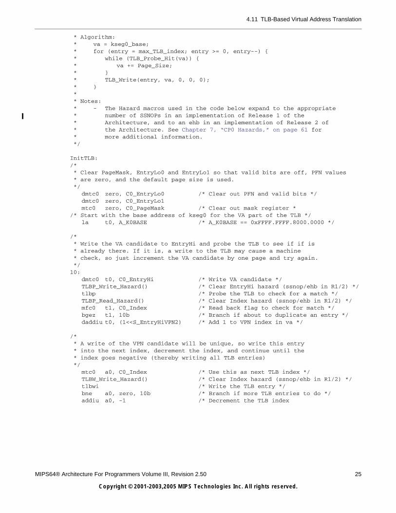
4.11 TLB-Based Virtual Address Translation
MIPS64® Architecture For Programmers Volume III, Revision 2.50 25
Copyright © 2001-2003,2005 MIPS Technologies Inc. All rights reserved.
* Algorithm:* va = kseg0_base;* for (entry = max_TLB_index; entry >= 0, entry--) {* while (TLB_Probe_Hit(va)) {* va += Page_Size;* }* TLB_Write(entry, va, 0, 0, 0);* }** Notes:* - The Hazard macros used in the code below expand to the appropriate* number of SSNOPs in an implementation of Release 1 of the* Architecture, and to an ehb in an implementation of Release 2 of* the Architecture. See Chapter 7, “CP0 Hazards,” on page 61 for* more additional information.*/
InitTLB:/** Clear PageMask, EntryLo0 and EntryLo1 so that valid bits are off, PFN values* are zero, and the default page size is used.*/
dmtc0 zero, C0_EntryLo0 /* Clear out PFN and valid bits */dmtc0 zero, C0_EntryLo1mtc0 zero, C0_PageMask /* Clear out mask register *
/* Start with the base address of kseg0 for the VA part of the TLB */la t0, A_K0BASE /* A_K0BASE == 0xFFFF.FFFF.8000.0000 */
/** Write the VA candidate to EntryHi and probe the TLB to see if if is* already there. If it is, a write to the TLB may cause a machine* check, so just increment the VA candidate by one page and try again.*/
10:dmtc0 t0, C0_EntryHi /* Write VA candidate */TLBP_Write_Hazard() /* Clear EntryHi hazard (ssnop/ehb in R1/2) */tlbp /* Probe the TLB to check for a match */TLBP_Read_Hazard() /* Clear Index hazard (ssnop/ehb in R1/2) */mfc0 t1, C0_Index /* Read back flag to check for match */bgez t1, 10b /* Branch if about to duplicate an entry */daddiu t0, (1<<S_EntryHiVPN2) /* Add 1 to VPN index in va */
/** A write of the VPN candidate will be unique, so write this entry* into the next index, decrement the index, and continue until the* index goes negative (thereby writing all TLB entries)*/
mtc0 a0, C0_Index /* Use this as next TLB index */TLBW_Write_Hazard() /* Clear Index hazard (ssnop/ehb in R1/2) */tlbwi /* Write the TLB entry */bne a0, zero, 10b /* Branch if more TLB entries to do */addiu a0, -1 /* Decrement the TLB index
26 MIPS64® Architecture For Programmers Volume III, Revision 2.50
Copyright © 2001-2003,2005 MIPS Technologies Inc. All rights reserved.
Chapter 4 Virtual Memory
/** Clear Index and EntryHi simply to leave the state constant for all* returns*/
mtc0 zero, C0_Indexdmtc0 zero, C0_EntryHijr ra /* Return to caller */nop
In the code above, 64-bit operations are shown for operations with the TLB. For MIPS64 processors which are running32-bit software, these instructions may be changed to the corresponding 32-bit instructions.
4.11.4 Address Translation
Release 2 of the Architecture introduced support for 1KB pages, and larger physical addresses. For clarity in thediscussion below, the following terms should be taken in the general sense to include the new Release 2 features:
When an address translation is requested, the virtual page number and the current process ASID are presented to theTLB. All entries are checked simultaneously for a match, which occurs when all of the following conditions are true:
• The current process ASID (as obtained from the EntryHi register) matches the ASID field in the TLB entry, or the Gbit is set in the TLB entry.
• Bits 63..62 of the virtual address match the region code in the R field of the TLB entry.
• The appropriate bits of the virtual page number match the corresponding bits of the VPN2 field stored within theTLB entry. The “appropriate” number of bits is determined by the Mask fields in each entry by ignoring each bit inthe virtual page number and the TLB VPN2 field corresponding to those bits that are set in the Mask fields. Thisallows each entry of the TLB to support a different page size, as determined by the PageMask register at the time thatthe TLB entry was written. If the recommended PageMask register is not implemented, the TLB operation is as if thePageMask register was written with the encoding for a 4KB page.
If a TLB entry matches the address and ASID presented, the corresponding PFN, C, V, and D bits are read from thetranslation section of the TLB entry. Which of the two PFN entries is read is a function of the virtual address bitimmediately to the right of the section masked with the Mask entry.
The valid and dirty bits determine the final success of the translation. If the valid bit is off, the entry is not valid and aTLB Invalid exception is raised. If the dirty bit is off and the reference was a store, a TLB Modified exception is raised.If there is an address match with a valid entry and no dirty exception, the PFN and the cache coherency bits are appendedto the offset-within-page bits of the address to form the final physical address with attributes.
Term Used Below Release 2 Substitution Comment
VPN2 VPN2 || VPN2X
Release 2 implementationsthat support 1KB pagesconcatenate the VPN2 andVPN2X fields to form thevirtual page number for a1KB page
PFN PFNX || PFN
Release 2 implementationsthat support larger physicaladdresses concatenate thePFNX and PFN fields to formthe physical page number
Mask Mask || MaskX
Release 2 implementationsthat support 1KB pagesconcatenate the Mask andMaskX fields to form thedon’t care mask for 1KBpages
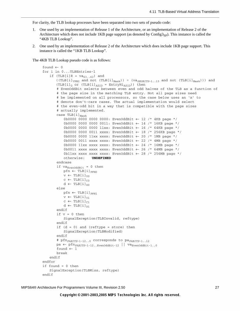
4.11 TLB-Based Virtual Address Translation
MIPS64® Architecture For Programmers Volume III, Revision 2.50 27
Copyright © 2001-2003,2005 MIPS Technologies Inc. All rights reserved.
For clarity, the TLB lookup processes have been separated into two sets of pseudo code:
1. One used by an implementation of Release 1 of the Architecture, or an implementation of Release 2 of theArchitecture which does not include 1KB page support (as denoted by Config3SP). This instance is called the“4KB TLB Lookup”.
2. One used by an implementation of Release 2 of the Architecture which does include 1KB page support. Thisinstance is called the “1KB TLB Lookup”.
The 4KB TLB Lookup pseudo code is as follows:
found ← 0for i in 0...TLBEntries-1
if (TLB[i]R = va63..62) and ((TLB[i]VPN2 and not (TLB[i]Mask)) = (vaSEGBITS-1..13 and not (TLB[i]Mask))) and (TLB[i]G or (TLB[i]ASID = EntryHiASID)) then
# EvenOddBit selects between even and odd halves of the TLB as a function of# the page size in the matching TLB entry. Not all page sizes need# be implemented on all processors, so the case below uses an ‘x’ to# denote don’t-care cases. The actual implementation would select# the even-odd bit in a way that is compatible with the page sizes# actually implemented.case TLB[i]Mask
0b0000 0000 0000 0000: EvenOddBit ← 12 /* 4KB page */0b0000 0000 0000 0011: EvenOddBit ← 14 /* 16KB page */0b0000 0000 0000 11xx: EvenOddBit ← 16 /* 64KB page */0b0000 0000 0011 xxxx: EvenOddBit ← 18 /* 256KB page */0b0000 0000 11xx xxxx: EvenOddBit ← 20 /* 1MB page */0b0000 0011 xxxx xxxx: EvenOddBit ← 22 /* 4MB page */0b0000 11xx xxxx xxxx: EvenOddBit ← 24 /* 16MB page */0b0011 xxxx xxxx xxxx: EvenOddBit ← 26 /* 64MB page */0b11xx xxxx xxxx xxxx: EvenOddBit ← 28 /* 256MB page */otherwise: UNDEFINED
endcaseif vaEvenOddBit = 0 then
pfn ← TLB[i]PFN0v ← TLB[i]V0c ← TLB[i]C0d ← TLB[i]D0
elsepfn ← TLB[i]PFN1v ← TLB[i]V1c ← TLB[i]C1d ← TLB[i]D1
endifif v = 0 then
SignalException(TLBInvalid, reftype)endifif (d = 0) and (reftype = store) then
SignalException(TLBModified)endif# pfnPABITS-1-12..0 corresponds to paPABITS-1..12pa ← pfnPABITS-1-12..EvenOddBit-12 || vaEvenOddBit-1..0found ← 1break
endifendforif found = 0 then
SignalException(TLBMiss, reftype)endif
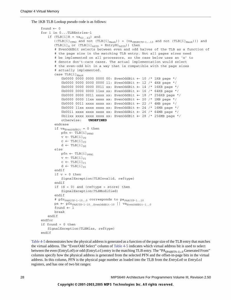
28 MIPS64® Architecture For Programmers Volume III, Revision 2.50
Copyright © 2001-2003,2005 MIPS Technologies Inc. All rights reserved.
Chapter 4 Virtual Memory
The 1KB TLB Lookup pseudo code is as follows:
found ← 0for i in 0...TLBEntries-1
if (TLB[i]R = va63..62) and ((TLB[i]VPN2 and not (TLB[i]Mask)) = (vaSEGBITS-1..13 and not (TLB[i]Mask))) and (TLB[i]G or (TLB[i]ASID = EntryHiASID)) then
# EvenOddBit selects between even and odd halves of the TLB as a function of# the page size in the matching TLB entry. Not all pages sizes need# be implemented on all processors, so the case below uses an ‘x’ to# denote don’t-care cases. The actual implementation would select# the even-odd bit in a way that is compatible with the page sizes# actually implemented.case TLB[i]Mask
0b0000 0000 0000 0000 00: EvenOddBit ← 10 /* 1KB page */0b0000 0000 0000 0000 11: EvenOddBit ← 12 /* 4KB page */0b0000 0000 0000 0011 xx: EvenOddBit ← 14 /* 16KB page */0b0000 0000 0000 11xx xx: EvenOddBit ← 16 /* 64KB page */0b0000 0000 0011 xxxx xx: EvenOddBit ← 18 /* 256KB page */0b0000 0000 11xx xxxx xx: EvenOddBit ← 20 /* 1MB page */0b0000 0011 xxxx xxxx xx: EvenOddBit ← 22 /* 4MB page */0b0000 11xx xxxx xxxx xx: EvenOddBit ← 24 /* 16MB page */0b0011 xxxx xxxx xxxx xx: EvenOddBit ← 26 /* 64MB page */0b11xx xxxx xxxx xxxx xx: EvenOddBit ← 28 /* 256MB page */otherwise: UNDEFINED
endcaseif vaEvenOddBit = 0 then
pfn ← TLB[i]PFN0v ← TLB[i]V0c ← TLB[i]C0d ← TLB[i]D0
elsepfn ← TLB[i]PFN1v ← TLB[i]V1c ← TLB[i]C1d ← TLB[i]D1
endifif v = 0 then
SignalException(TLBInvalid, reftype)endifif (d = 0) and (reftype = store) then
SignalException(TLBModified)endif# pfnPABITS-1-10..0 corresponds to paPABITS-1..10pa ← pfnPABITS-1-10..EvenOddBit-10 || vaEvenOddBit-1..0found ← 1break
endifendforif found = 0 then
SignalException(TLBMiss, reftype)endif
Table 4-5 demonstrates how the physical address is generated as a function of the page size of the TLB entry that matchesthe virtual address. The “Even/Odd Select” column of Table 4-5 indicates which virtual address bit is used to selectbetween the even (EntryLo0) or odd (EntryLo1) entry in the matching TLB entry. The “PA(PABITS-1)..0 Generated From”columns specify how the physical address is generated from the selected PFN and the offset-in-page bits in the virtualaddress. In this column, PFN is the physical page number as loaded into the TLB from the EntryLo0 or EntryLo1registers, and has one of two bit ranges:
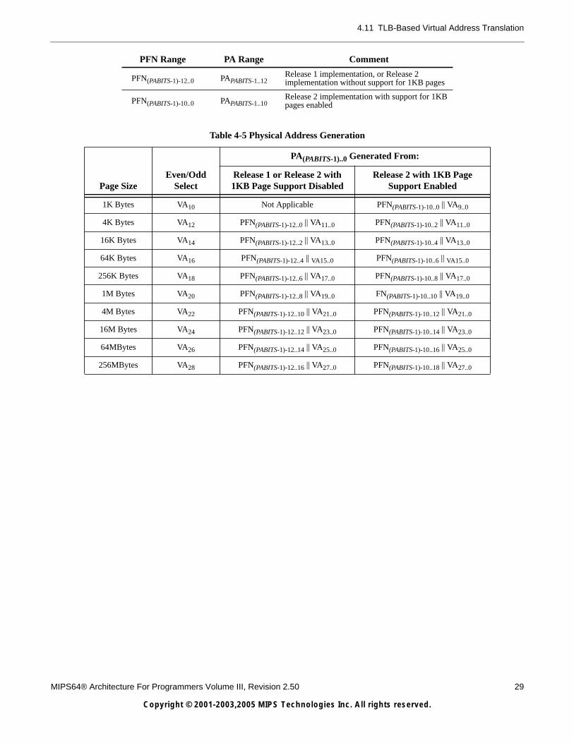
4.11 TLB-Based Virtual Address Translation
MIPS64® Architecture For Programmers Volume III, Revision 2.50 29
Copyright © 2001-2003,2005 MIPS Technologies Inc. All rights reserved.
PFN Range PA Range Comment
PFN(PABITS-1)-12..0 PAPABITS-1..12Release 1 implementation, or Release 2implementation without support for 1KB pages
PFN(PABITS-1)-10..0 PAPABITS-1..10Release 2 implementation with support for 1KBpages enabled
Table 4-5 Physical Address Generation
Page SizeEven/Odd
Select
PA(PABITS-1)..0 Generated From:
Release 1 or Release 2 with1KB Page Support Disabled
Release 2 with 1KB PageSupport Enabled
1K Bytes VA10 Not Applicable PFN(PABITS-1)-10..0 || VA9..0
4K Bytes VA12 PFN(PABITS-1)-12..0 || VA11..0 PFN(PABITS-1)-10..2 || VA11..0
16K Bytes VA14 PFN(PABITS-1)-12..2 || VA13..0 PFN(PABITS-1)-10..4 || VA13..0
64K Bytes VA16 PFN(PABITS-1)-12..4 || VA15..0 PFN(PABITS-1)-10..6 || VA15..0
256K Bytes VA18 PFN(PABITS-1)-12..6 || VA17..0 PFN(PABITS-1)-10..8 || VA17..0
1M Bytes VA20 PFN(PABITS-1)-12..8 || VA19..0 FN(PABITS-1)-10..10 || VA19..0
4M Bytes VA22 PFN(PABITS-1)-12..10 || VA21..0 PFN(PABITS-1)-10..12 || VA21..0
16M Bytes VA24 PFN(PABITS-1)-12..12 || VA23..0 PFN(PABITS-1)-10..14 || VA23..0
64MBytes VA26 PFN(PABITS-1)-12..14 || VA25..0 PFN(PABITS-1)-10..16 || VA25..0
256MBytes VA28 PFN(PABITS-1)-12..16 || VA27..0 PFN(PABITS-1)-10..18 || VA27..0

30 MIPS64® Architecture For Programmers Volume III, Revision 2.50
Copyright © 2001-2003,2005 MIPS Technologies Inc. All rights reserved.
Chapter 4 Virtual Memory
MIPS64® Architecture For Programmers Volume III, Revision 2.50 31
Copyright © 2001-2003,2005 MIPS Technologies Inc. All rights reserved.
Chapter 5
Interrupts and Exceptions
Release 2 of the Architecture added the following features related to the processing of Exceptions and Interrupts:
• The addition of the Coprocessor 0 EBase register, which allows the exception vector base address to be modified forexceptions that occur when StatusBEV equals 0. The EBase register is required.
• The extension of the Release 1 interrupt control mechanism to include two optional interrupt modes:
• Vectored Interrupt (VI) mode, in which the various sources of interrupts are prioritized by the processor and eachinterrupt is vectored directly to a dedicated handler. When combined with GPR shadow registers, introduced inthe next chapter, this mode significantly reduces the number of cycles required to process an interrupt.
• External Interrupt Controller (EIC) mode, in which the definition of the coprocessor 0 register fields associatedwith interrupts changes to support an external interrupt controller. This can support many more prioritizedinterrupts, while still providing the ability to vector an interrupt directly to a dedicated handler and takeadvantage of the GPR shadow registers.
• The ability to stop the Count register for highly power-sensitive applications in which the Count register is not used,or for reduced power mode. This change is required.
• The addition of the DI and EI instructions which provide the ability to atomically disable or enable interrupts. Bothinstructions are required.
• The addition of the TI and PCI bits in the Cause register to denote pending timer and performance counter interrupts.This change is required.
• The addition of an execution hazard sequence which can be used to clear hazards introduced when software writes toa coprocessor 0 register which affects the interrupt system state.
5.1 Interrupts
Release 1 of the Architecture included support for two software interrupts, six hardware interrupts, and twospecial-purpose interrupts: timer and performance counter. The timer and performance counter interrupts were combinedwith hardware interrupt 5 in an implementation-dependent manner. Interrupts were handled either through the generalexception vector (offset 0x180) or the special interrupt vector (0x200), based on the value of CauseIV. Software wasrequired to prioritize interrupts as a function of the CauseIP bits in the interrupt handler prologue.
Release 2 of the Architecture adds an upward-compatible extension to the Release 1 interrupt architecture that supportsvectored interrupts. In addition, Release 2 adds a new interrupt mode that supports the use of an external interruptcontroller by changing the interrupt architecture.
Although a Non-Maskable Interrupt (NMI) includes “interrupt” in its name, it is more correctly described as an NMIexception because it does not affect, nor is it controlled by the processor interrupt system.
An interrupt is only taken when all of the following are true:
• A specific request for interrupt service is made, as a function of the interrupt mode, described below.
• The IE bit in the Status register is a one.
• The DM bit in the Debug register is a zero (for processors implementing EJTAG)
• The EXL and ERL bits in the Status register are both zero.
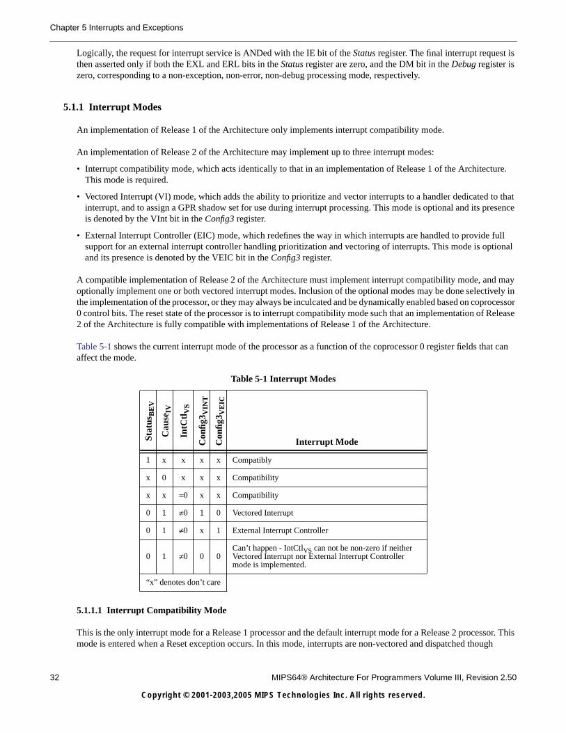
32 MIPS64® Architecture For Programmers Volume III, Revision 2.50
Copyright © 2001-2003,2005 MIPS Technologies Inc. All rights reserved.
Chapter 5 Interrupts and Exceptions
Logically, the request for interrupt service is ANDed with the IE bit of the Status register. The final interrupt request isthen asserted only if both the EXL and ERL bits in the Status register are zero, and the DM bit in the Debug register iszero, corresponding to a non-exception, non-error, non-debug processing mode, respectively.
5.1.1 Interrupt Modes
An implementation of Release 1 of the Architecture only implements interrupt compatibility mode.
An implementation of Release 2 of the Architecture may implement up to three interrupt modes:
• Interrupt compatibility mode, which acts identically to that in an implementation of Release 1 of the Architecture.This mode is required.
• Vectored Interrupt (VI) mode, which adds the ability to prioritize and vector interrupts to a handler dedicated to thatinterrupt, and to assign a GPR shadow set for use during interrupt processing. This mode is optional and its presenceis denoted by the VInt bit in the Config3 register.
• External Interrupt Controller (EIC) mode, which redefines the way in which interrupts are handled to provide fullsupport for an external interrupt controller handling prioritization and vectoring of interrupts. This mode is optionaland its presence is denoted by the VEIC bit in the Config3 register.
A compatible implementation of Release 2 of the Architecture must implement interrupt compatibility mode, and mayoptionally implement one or both vectored interrupt modes. Inclusion of the optional modes may be done selectively inthe implementation of the processor, or they may always be inculcated and be dynamically enabled based on coprocessor0 control bits. The reset state of the processor is to interrupt compatibility mode such that an implementation of Release2 of the Architecture is fully compatible with implementations of Release 1 of the Architecture.
Table 5-1 shows the current interrupt mode of the processor as a function of the coprocessor 0 register fields that canaffect the mode.
5.1.1.1 Interrupt Compatibility Mode
This is the only interrupt mode for a Release 1 processor and the default interrupt mode for a Release 2 processor. Thismode is entered when a Reset exception occurs. In this mode, interrupts are non-vectored and dispatched though
Table 5-1 Interrupt Modes
Stat
usB
EV
Cau
seIV
IntC
tlV
S
Con
fig3 V
INT
Con
fig3 V
EIC
Interrupt Mode
1 x x x x Compatibly
x 0 x x x Compatibility
x x =0 x x Compatibility
0 1 ≠0 1 0 Vectored Interrupt
0 1 ≠0 x 1 External Interrupt Controller
0 1 ≠0 0 0Can’t happen - IntCtlVS can not be non-zero if neitherVectored Interrupt nor External Interrupt Controllermode is implemented.
“x” denotes don’t care
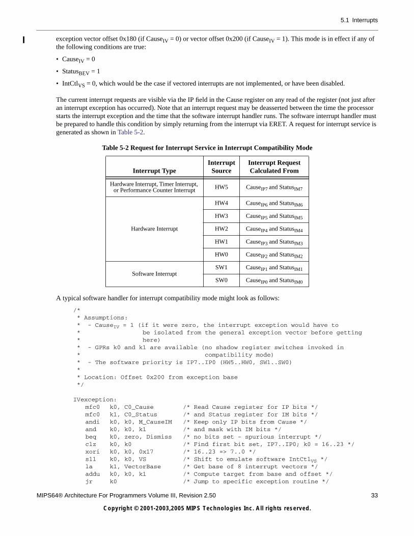
5.1 Interrupts
MIPS64® Architecture For Programmers Volume III, Revision 2.50 33
Copyright © 2001-2003,2005 MIPS Technologies Inc. All rights reserved.
exception vector offset 0x180 (if CauseIV = 0) or vector offset 0x200 (if CauseIV = 1). This mode is in effect if any ofthe following conditions are true:
• CauseIV = 0
• StatusBEV = 1
• IntCtlVS = 0, which would be the case if vectored interrupts are not implemented, or have been disabled.
The current interrupt requests are visible via the IP field in the Cause register on any read of the register (not just afteran interrupt exception has occurred). Note that an interrupt request may be deasserted between the time the processorstarts the interrupt exception and the time that the software interrupt handler runs. The software interrupt handler mustbe prepared to handle this condition by simply returning from the interrupt via ERET. A request for interrupt service isgenerated as shown in Table 5-2.
A typical software handler for interrupt compatibility mode might look as follows:
/* * Assumptions: * - CauseIV = 1 (if it were zero, the interrupt exception would have to * be isolated from the general exception vector before getting * here) * - GPRs k0 and k1 are available (no shadow register switches invoked in * compatibility mode) * - The software priority is IP7..IP0 (HW5..HW0, SW1..SW0) * * Location: Offset 0x200 from exception base */
IVexception:mfc0 k0, C0_Cause /* Read Cause register for IP bits */mfc0 k1, C0_Status /* and Status register for IM bits */andi k0, k0, M_CauseIM /* Keep only IP bits from Cause */and k0, k0, k1 /* and mask with IM bits */beq k0, zero, Dismiss /* no bits set - spurious interrupt */clz k0, k0 /* Find first bit set, IP7..IP0; k0 = 16..23 */xori k0, k0, 0x17 /* 16..23 => 7..0 */sll k0, k0, VS /* Shift to emulate software IntCtlVS */la k1, VectorBase /* Get base of 8 interrupt vectors */addu k0, k0, k1 /* Compute target from base and offset */jr k0 /* Jump to specific exception routine */
Table 5-2 Request for Interrupt Service in Interrupt Compatibility Mode
Interrupt TypeInterrupt
SourceInterrupt RequestCalculated From
Hardware Interrupt, Timer Interrupt,or Performance Counter Interrupt HW5 CauseIP7 and StatusIM7
Hardware Interrupt
HW4 CauseIP6 and StatusIM6
HW3 CauseIP5 and StatusIM5
HW2 CauseIP4 and StatusIM4
HW1 CauseIP3 and StatusIM3
HW0 CauseIP2 and StatusIM2
Software InterruptSW1 CauseIP1 and StatusIM1
SW0 CauseIP0 and StatusIM0
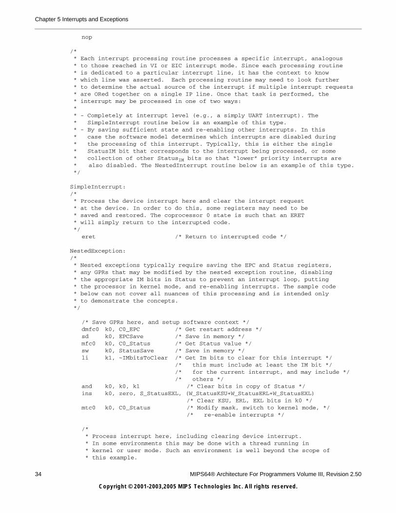
34 MIPS64® Architecture For Programmers Volume III, Revision 2.50
Copyright © 2001-2003,2005 MIPS Technologies Inc. All rights reserved.
Chapter 5 Interrupts and Exceptions
nop
/* * Each interrupt processing routine processes a specific interrupt, analogous * to those reached in VI or EIC interrupt mode. Since each processing routine * is dedicated to a particular interrupt line, it has the context to know * which line was asserted. Each processing routine may need to look further * to determine the actual source of the interrupt if multiple interrupt requests * are ORed together on a single IP line. Once that task is performed, the * interrupt may be processed in one of two ways: * * - Completely at interrupt level (e.g., a simply UART interrupt). The * SimpleInterrupt routine below is an example of this type. * - By saving sufficient state and re-enabling other interrupts. In this * case the software model determines which interrupts are disabled during * the processing of this interrupt. Typically, this is either the single * StatusIM bit that corresponds to the interrupt being processed, or some * collection of other StatusIM bits so that “lower” priority interrupts are * also disabled. The NestedInterrupt routine below is an example of this type. */
SimpleInterrupt:/* * Process the device interrupt here and clear the interupt request * at the device. In order to do this, some registers may need to be * saved and restored. The coprocessor 0 state is such that an ERET * will simply return to the interrupted code. */
eret /* Return to interrupted code */
NestedException:/* * Nested exceptions typically require saving the EPC and Status registers, * any GPRs that may be modified by the nested exception routine, disabling * the appropriate IM bits in Status to prevent an interrupt loop, putting * the processor in kernel mode, and re-enabling interrupts. The sample code * below can not cover all nuances of this processing and is intended only * to demonstrate the concepts. */
/* Save GPRs here, and setup software context */dmfc0 k0, C0_EPC /* Get restart address */sd k0, EPCSave /* Save in memory */mfc0 k0, C0_Status /* Get Status value */sw k0, StatusSave /* Save in memory */li k1, ~IMbitsToClear /* Get Im bits to clear for this interrupt */
/* this must include at least the IM bit *//* for the current interrupt, and may include *//* others */
and k0, k0, k1 /* Clear bits in copy of Status */ins k0, zero, S_StatusEXL, (W_StatusKSU+W_StatusERL+W_StatusEXL)
/* Clear KSU, ERL, EXL bits in k0 */mtc0 k0, C0_Status /* Modify mask, switch to kernel mode, */
/* re-enable interrupts */
/* * Process interrupt here, including clearing device interrupt. * In some environments this may be done with a thread running in * kernel or user mode. Such an environment is well beyond the scope of * this example.

5.1 Interrupts
MIPS64® Architecture For Programmers Volume III, Revision 2.50 35
Copyright © 2001-2003,2005 MIPS Technologies Inc. All rights reserved.
*/
/* * To complete interrupt processing, the saved values must be restored * and the original interrupted code restarted. */
di /* Disable interrupts - may not be required */lw k0, StatusSave /* Get saved Status (including EXL set) */ld k1, EPCSave /* and EPC */mtc0 k0, C0_Status /* Restore the original value */dmtc0 k1, C0_EPC /* and EPC *//* Restore GPRs and software state */eret /* Dismiss the interrupt */
5.1.1.2 Vectored Interrupt Mode
Vectored Interrupt mode builds on the interrupt compatibility mode by adding a priority encoder to prioritize pendinginterrupts and to generate a vector with which each interrupt can be directed to a dedicated handler routine. This modealso allows each interrupt to be mapped to a GPR shadow set for use by the interrupt handler. Vectored Interrupt modeis in effect if all of the following conditions are true:
• Config3VInt = 1
• Config3VEIC = 0
• IntCtlVS ≠ 0
• CauseIV = 1
• StatusBEV = 0
In VI interrupt mode, the six hardware interrupts are interpreted as individual hardware interrupt requests. The timer andperformance counter interrupts are combined in an implementation-dependent way with the hardware interrupts (withthe interrupt with which they are combined indicated by IntCtlIPTI and IntCtlIPPCI, respectively) to provide theappropriate relative priority of these interrupts with that of the hardware interrupts. The processor interrupt logic ANDseach of the CauseIP bits with the corresponding StatusIM bits. If any of these values is 1, and if interrupts are enabled(StatusIE = 1, StatusEXL = 0, and StatusERL = 0), an interrupt is signaled and a priority encoder scans the values in theorder shown in Table 5-3.
Table 5-3 Relative Interrupt Priority for Vectored Interrupt Mode
RelativePriority
InterruptType
InterruptSource
Interrupt RequestCalculated From
Vector NumberGenerated by
Priority Encoder
Highest Priority
Hardware
HW5 CauseIP7 and StatusIM7 7
HW4 CauseIP6 and StatusIM6 6
HW3 CauseIP5 and StatusIM5 5
HW2 CauseIP4 and StatusIM4 4
HW1 CauseIP3 and StatusIM3 3
HW0 CauseIP2 and StatusIM2 2
SoftwareSW1 CauseIP1 and StatusIM1 1
Lowest Priority SW0 CauseIP0 and StatusIM0 0
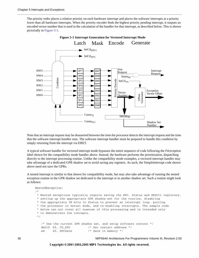
36 MIPS64® Architecture For Programmers Volume III, Revision 2.50
Copyright © 2001-2003,2005 MIPS Technologies Inc. All rights reserved.
Chapter 5 Interrupts and Exceptions
The priority order places a relative priority on each hardware interrupt and places the software interrupts at a prioritylower than all hardware interrupts. When the priority encoder finds the highest priority pending interrupt, it outputs anencoded vector number that is used in the calculation of the handler for that interrupt, as described below. This is shownpictorially in Figure 5-1.
Note that an interrupt request may be deasserted between the time the processor detects the interrupt request and the timethat the software interrupt handler runs. The software interrupt handler must be prepared to handle this condition bysimply returning from the interrupt via ERET.
A typical software handler for vectored interrupt mode bypasses the entire sequence of code following the IVexceptionlabel shown for the compatibility mode handler above. Instead, the hardware performs the prioritization, dispatchingdirectly to the interrupt processing routine. Unlike the compatibility mode examples, a vectored interrupt handler maytake advantage of a dedicated GPR shadow set to avoid saving any registers. As such, the SimpleInterrupt code shownabove need not save the GPRs.
A nested interrupt is similar to that shown for compatibility mode, but may also take advantage of running the nestedexception routine in the GPR shadow set dedicated to the interrupt or in another shadow set. Such a routine might lookas follows:
NestedException:/* * Nested exceptions typically require saving the EPC, Status and SRSCtl registers, * setting up the appropriate GPR shadow set for the routine, disabling * the appropriate IM bits in Status to prevent an interrupt loop, putting * the processor in kernel mode, and re-enabling interrupts. The sample code * below can not cover all nuances of this processing and is intended only * to demonstrate the concepts. */
/* Use the current GPR shadow set, and setup software context */dmfc0 k0, C0_EPC /* Get restart address */sd k0, EPCSave /* Save in memory */
IP7
IP6
IP5
IP4
IP3
IP2
IP1
IP0
IM7
IM6
IM5
IM4
IM3
IM2
IM1
IM0
Prio
rity
Enc
ode
HW5
HW4
HW3
HW2
HW1
HW0
Com
bine
CauseTI
CausePCI
StatusIE
InterruptRequest
VectorNumber
Latch Mask EncodeFigure 5-1 Interrupt Generation for Vectored Interrupt Mode
AnyRequest
Off
set
Gen
erat
or
IntCtlVS
ExceptionVector Offset
Generate
SRSMap
Shadow SetNumber
IntCtlIPPCI
IntCtlIPTI
5.1 Interrupts
MIPS64® Architecture For Programmers Volume III, Revision 2.50 37
Copyright © 2001-2003,2005 MIPS Technologies Inc. All rights reserved.
mfc0 k0, C0_Status /* Get Status value */sw k0, StatusSave /* Save in memory */mfc0 k0, C0_SRSCtl /* Save SRSCtl if changing shadow sets */sw k0, SRSCtlSaveli k1, ~IMbitsToClear /* Get Im bits to clear for this interrupt */
/* this must include at least the IM bit *//* for the current interrupt, and may include *//* others */
and k0, k0, k1 /* Clear bits in copy of Status *//* If switching shadow sets, write new value to SRSCtlPSS here */ins k0, zero, S_StatusEXL, (W_StatusKSU+W_StatusERL+W_StatusEXL)
/* Clear KSU, ERL, EXL bits in k0 */mtc0 k0, C0_Status /* Modify mask, switch to kernel mode, */
/* re-enable interrupts *//* * If switching shadow sets, clear only KSU above, write target * address to EPC, and do execute an eret to clear EXL, switch * shadow sets, and jump to routine */
/* Process interrupt here, including clearing device interrupt */
/* * To complete interrupt processing, the saved values must be restored * and the original interrupted code restarted. */
di /* Disable interrupts - may not be required */lw k0, StatusSave /* Get saved Status (including EXL set) */ld k1, EPCSave /* and EPC */mtc0 k0, C0_Status /* Restore the original value */lw k0, SRSCtlSave /* Get saved SRSCtl */dmtc0 k1, C0_EPC /* and EPC */mtc0 k0, C0_SRSCtl /* Restore shadow sets */ehb /* Clear hazard */eret /* Dismiss the interrupt */
5.1.1.3 External Interrupt Controller Mode
External Interrupt Controller Mode redefines the way that the processor interrupt logic is configured to provide supportfor an external interrupt controller. The interrupt controller is responsible for prioritizing all interrupts, includinghardware, software, timer, and performance counter interrupts, and directly supplying to the processor the vector numberof the highest priority interrupt. EIC interrupt mode is in effect if all of the following conditions are true:
• Config3VEIC = 1
• IntCtlVS ≠ 0
• CauseIV = 1
• StatusBEV = 0
In EIC interrupt mode, the processor sends the state of the software interrupt requests (CauseIP1..IP0), the timer interruptrequest (CauseTI), and the performance counter interrupt request (CausePCI) to the external interrupt controller, whereit prioritizes these interrupts in a system-dependent way with other hardware interrupts. The interrupt controller can bea hard-wired logic block, or it can be configurable based on control and status registers. This allows the interruptcontroller to be more specific or more general as a function of the system environment and needs.
The external interrupt controller prioritizes its interrupt requests and produces the vector number of the highest priorityinterrupt to be serviced. The vector number, called the Requested Interrupt Priority Level (RIPL), is a 6-bit encoded

38 MIPS64® Architecture For Programmers Volume III, Revision 2.50
Copyright © 2001-2003,2005 MIPS Technologies Inc. All rights reserved.
Chapter 5 Interrupts and Exceptions
value in the range 0..63, inclusive. A value of 0 indicates that no interrupt requests are pending. The values 1..63represent the lowest (1) to highest (63) RIPL for the interrupt to be serviced. The interrupt controller passes this valueon the 6 hardware interrupt line, which are treated as an encoded value in EIC interrupt mode.
StatusIPL (which overlays StatusIM7..IM2) is interpreted as the Interrupt Priority Level (IPL) at which the processor iscurrently operating (with a value of zero indicating that no interrupt is currently being serviced). When the interruptcontroller requests service for an interrupt, the processor compares RIPL with StatusIPL to determine if the requestedinterrupt has higher priority than the current IPL. If RIPL is strictly greater than StatusIPL, and interrupts are enabled(StatusIE = 1, StatusEXL = 0, and StatusERL = 0) an interrupt request is signaled to the pipeline. When the processor startsthe interrupt exception, it loads RIPL into CauseRIPL (which overlays CauseIP7..IP2) and signals the external interruptcontroller to notify it that the request is being serviced. The interrupt exception uses the value of CauseRIPL as the vectornumber. Because CauseRIPL is only loaded by the processor when an interrupt exception is signaled, it is available tosoftware during interrupt processing.
In EIC interrupt mode, the external interrupt controller is also responsible for supplying the GPR shadow set number touse when servicing the interrupt. As such, the SRSMap register is not used in this mode, and the mapping of the vectoredinterrupt to a GPR shadow set is done by programming (or designing) the interrupt controller to provide the correct GPRshadow set number when an interrupt is requested. When the processor loads an interrupt request into CauseRIPL, it alsoloads the GPR shadow set number into SRSCtlEICSS, which is copied to SRSCtlCSS when the interrupt is serviced.
The operation of EIC interrupt mode is shown pictorially in Figure 5-2.
A typical software handler for EIC interrupt mode bypasses the entire sequence of code following the IVexception
label shown for the compatibility mode handler above. Instead, the hardware performs the prioritization, dispatchingdirectly to the interrupt processing routine. Unlike the compatibility mode examples, an EIC interrupt handler may takeadvantage of a dedicated GPR shadow set to avoid saving any registers. As such, the SimpleInterrupt code shown aboveneed not save the GPRs.
CauseTICausePCI
StatusIE
InterruptRequest
VectorNumber
Latch CompareEncodeFigure 5-2 Interrupt Generation for External Interrupt Controller Interrupt Mode
AnyRequest
Off
set
Gen
erat
or
IntCtlVS
ExceptionVector Offset
Generate
Shadow SetNumber
Ext
erna
l Int
erru
pt C
ontr
olle
r
Inte
rrup
t Sou
rces
Shad
ow S
etM
appi
ng
CauseIP1CauseIP0
RequestedIPL
Cau
seR
IPL
Stat
usIP
L
SRSC
tl EIC
SS
RIPL>
IPL?
LoadFields
InterruptException
Interrupt ServiceStarted
5.1 Interrupts
MIPS64® Architecture For Programmers Volume III, Revision 2.50 39
Copyright © 2001-2003,2005 MIPS Technologies Inc. All rights reserved.
A nested interrupt is similar to that shown for compatibility mode, but may also take advantage of running the nestedexception routine in the GPR shadow set dedicated to the interrupt or in another shadow set. It also need only copyCauseRIPL to StatusIPL to prevent lower priority interrupts from interrupting the handler. Such a routine might look asfollows:
NestedException:/* * Nested exceptions typically require saving the EPC, Status,and SRSCtl registers, * setting up the appropriate GPR shadow set for the routine, disabling * the appropriate IM bits in Status to prevent an interrupt loop, putting * the processor in kernel mode, and re-enabling interrupts. The sample code * below can not cover all nuances of this processing and is intended only * to demonstrate the concepts. */
/* Use the current GPR shadow set, and setup software context */mfc0 k1, C0_Cause /* Read Cause to get RIPL value */dmfc0 k0, C0_EPC /* Get restart address */srl k1, k1, S_CauseRIPL /* Right justify RIPL field */sd k0, EPCSave /* Save in memory */mfc0 k0, C0_Status /* Get Status value */sw k0, StatusSave /* Save in memory */ins k0, k1, S_StatusIPL, 6 /* Set IPL to RIPL in copy of Status */mfc0 k1, C0_SRSCtl /* Save SRSCtl if changing shadow sets */sw k1, SRSCtlSave/* If switching shadow sets, write new value to SRSCtlPSS here */ins k0, zero, S_StatusEXL, (W_StatusKSU+W_StatusERL+W_StatusEXL)
/* Clear KSU, ERL, EXL bits in k0 */mtc0 k0, C0_Status /* Modify IPL, switch to kernel mode, */
/* re-enable interrupts *//* * If switching shadow sets, clear only KSU above, write target * address to EPC, and do execute an eret to clear EXL, switch * shadow sets, and jump to routine */
/* Process interrupt here, including clearing device interrupt */
/* * The interrupt completion code is identical to that shown for VI mode above. */
5.1.2 Generation of Exception Vector Offsets for Vectored Interrupts
For vectored interrupts (in either VI or EIC interrupt mode), a vector number is produced by the interrupt control logic.This number is combined with IntCtlVS to create the interrupt offset, which is added to 0x200 to create the exceptionvector offset. For VI interrupt mode, the vector number is in the range 0..7, inclusive. For EIC interrupt mode, the vectornumber is in the range 1..63, inclusive (0 being the encoding for “no interrupt”). The IntCtlVS field specifies the spacingbetween vector locations. If this value is zero (the default reset state), the vector spacing is zero and the processor revertsto Interrupt Compatibility Mode. A non-zero value enables vectored interrupts, and Table 5-4 shows the exceptionvector offset for a representative subset of the vector numbers and values of the IntCtlVS field.
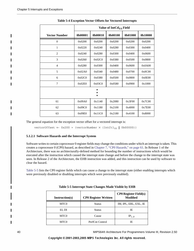
40 MIPS64® Architecture For Programmers Volume III, Revision 2.50
Copyright © 2001-2003,2005 MIPS Technologies Inc. All rights reserved.
Chapter 5 Interrupts and Exceptions
The general equation for the exception vector offset for a vectored interrupt is:
vectorOffset ← 0x200 + (vectorNumber × (IntCtlVS || 0b00000))
5.1.2.1 Software Hazards and the Interrupt System
Software writes to certain coprocessor 0 register fields may change the conditions under which an interrupt is taken. Thiscreates a coprocessor 0 (CP0) hazard, as described in Chapter 7, “CP0 Hazards,” on page 61. In Release 1 of theArchitecture, there was no architecturally-defined method for bounding the number of instructions which would beexecuted after the instruction which caused the interrupt state change and before the change to the interrupt state wasseen. In Release 2 of the Architecture, the EHB instruction was added, and this instruction can be used by software toclear the hazard.
Table 5-5 lists the CP0 register fields which can cause a change to the interrupt state (either enabling interrupts whichwere previously disabled or disabling interrupts which were previously enabled).
Table 5-4 Exception Vector Offsets for Vectored Interrupts
Vector Number
Value of IntCtlVS Field
0b00001 0b00010 0b00100 0b01000 0b10000
0 0x0200 0x0200 0x0200 0x0200 0x0200
1 0x0220 0x0240 0x0280 0x0300 0x0400
2 0x0240 0x0280 0x0300 0x0400 0x0600
3 0x0260 0x02C0 0x0380 0x0500 0x0800
4 0x0280 0x0300 0x0400 0x0600 0x0A00
5 0x02A0 0x0340 0x0480 0x0700 0x0C00
6 0x02C0 0x0380 0x0500 0x0800 0x0E00
7 0x02E0 0x03C0 0x0580 0x0900 0x1000
•••
61 0x09A0 0x1140 0x2080 0x3F00 0x7C00
62 0x09C0 0x1180 0x2100 0x4000 0x7E00
63 0x09E0 0x11C0 0x2180 0x4100 0x8000
Table 5-5 Interrupt State Changes Made Visible by EHB
Instruction(s) CP0 Register WrittenCP0 Register Field(s)
Modified
MTC0 Status IM, IPL, ERL, EXL, IE
EI, DI Status IE
MTC0 Cause IP1..0
MTC0 PerfCnt Control IE
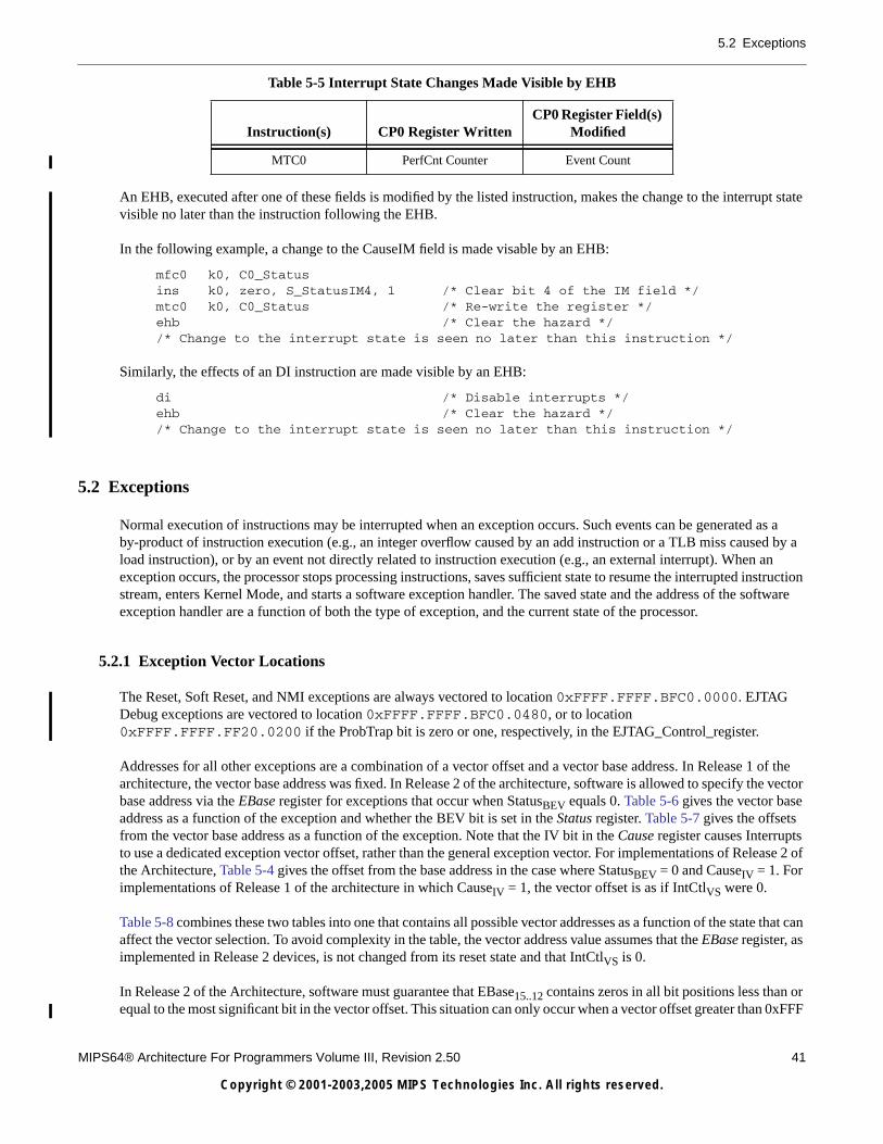
5.2 Exceptions
MIPS64® Architecture For Programmers Volume III, Revision 2.50 41
Copyright © 2001-2003,2005 MIPS Technologies Inc. All rights reserved.
An EHB, executed after one of these fields is modified by the listed instruction, makes the change to the interrupt statevisible no later than the instruction following the EHB.
In the following example, a change to the CauseIM field is made visable by an EHB:
mfc0 k0, C0_Statusins k0, zero, S_StatusIM4, 1 /* Clear bit 4 of the IM field */mtc0 k0, C0_Status /* Re-write the register */ehb /* Clear the hazard *//* Change to the interrupt state is seen no later than this instruction */
Similarly, the effects of an DI instruction are made visible by an EHB:
di /* Disable interrupts */ehb /* Clear the hazard *//* Change to the interrupt state is seen no later than this instruction */
5.2 Exceptions
Normal execution of instructions may be interrupted when an exception occurs. Such events can be generated as aby-product of instruction execution (e.g., an integer overflow caused by an add instruction or a TLB miss caused by aload instruction), or by an event not directly related to instruction execution (e.g., an external interrupt). When anexception occurs, the processor stops processing instructions, saves sufficient state to resume the interrupted instructionstream, enters Kernel Mode, and starts a software exception handler. The saved state and the address of the softwareexception handler are a function of both the type of exception, and the current state of the processor.
5.2.1 Exception Vector Locations
The Reset, Soft Reset, and NMI exceptions are always vectored to location 0xFFFF.FFFF.BFC0.0000. EJTAGDebug exceptions are vectored to location 0xFFFF.FFFF.BFC0.0480, or to location0xFFFF.FFFF.FF20.0200 if the ProbTrap bit is zero or one, respectively, in the EJTAG_Control_register.
Addresses for all other exceptions are a combination of a vector offset and a vector base address. In Release 1 of thearchitecture, the vector base address was fixed. In Release 2 of the architecture, software is allowed to specify the vectorbase address via the EBase register for exceptions that occur when StatusBEV equals 0. Table 5-6 gives the vector baseaddress as a function of the exception and whether the BEV bit is set in the Status register. Table 5-7 gives the offsetsfrom the vector base address as a function of the exception. Note that the IV bit in the Cause register causes Interruptsto use a dedicated exception vector offset, rather than the general exception vector. For implementations of Release 2 ofthe Architecture, Table 5-4 gives the offset from the base address in the case where StatusBEV = 0 and CauseIV = 1. Forimplementations of Release 1 of the architecture in which CauseIV = 1, the vector offset is as if IntCtlVS were 0.
Table 5-8 combines these two tables into one that contains all possible vector addresses as a function of the state that canaffect the vector selection. To avoid complexity in the table, the vector address value assumes that the EBase register, asimplemented in Release 2 devices, is not changed from its reset state and that IntCtlVS is 0.
In Release 2 of the Architecture, software must guarantee that EBase15..12 contains zeros in all bit positions less than orequal to the most significant bit in the vector offset. This situation can only occur when a vector offset greater than 0xFFF
MTC0 PerfCnt Counter Event Count
Table 5-5 Interrupt State Changes Made Visible by EHB
Instruction(s) CP0 Register WrittenCP0 Register Field(s)
Modified
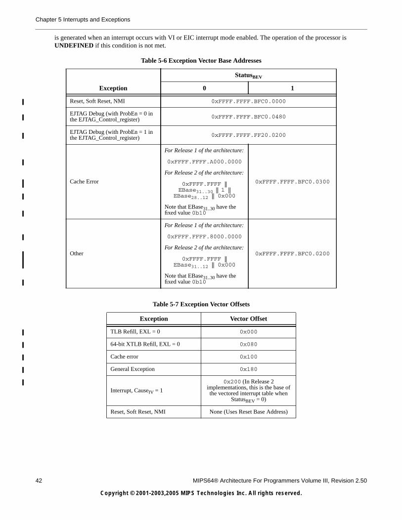
42 MIPS64® Architecture For Programmers Volume III, Revision 2.50
Copyright © 2001-2003,2005 MIPS Technologies Inc. All rights reserved.
Chapter 5 Interrupts and Exceptions
is generated when an interrupt occurs with VI or EIC interrupt mode enabled. The operation of the processor isUNDEFINED if this condition is not met.
Table 5-6 Exception Vector Base Addresses
Exception
StatusBEV
0 1
Reset, Soft Reset, NMI 0xFFFF.FFFF.BFC0.0000
EJTAG Debug (with ProbEn = 0 inthe EJTAG_Control_register) 0xFFFF.FFFF.BFC0.0480
EJTAG Debug (with ProbEn = 1 inthe EJTAG_Control_register) 0xFFFF.FFFF.FF20.0200
Cache Error
For Release 1 of the architecture:
0xFFFF.FFFF.A000.0000
For Release 2 of the architecture:
0xFFFF.FFFF ||EBase31..30 || 1 ||
EBase28..12 || 0x000
Note that EBase31..30 have thefixed value 0b10
0xFFFF.FFFF.BFC0.0300
Other
For Release 1 of the architecture:
0xFFFF.FFFF.8000.0000
For Release 2 of the architecture:
0xFFFF.FFFF ||EBase31..12 || 0x000
Note that EBase31..30 have thefixed value 0b10
0xFFFF.FFFF.BFC0.0200
Table 5-7 Exception Vector Offsets
Exception Vector Offset
TLB Refill, EXL = 0 0x000
64-bit XTLB Refill, EXL = 0 0x080
Cache error 0x100
General Exception 0x180
Interrupt, CauseIV = 1
0x200 (In Release 2implementations, this is the base ofthe vectored interrupt table when
StatusBEV = 0)
Reset, Soft Reset, NMI None (Uses Reset Base Address)

5.2 Exceptions
MIPS64® Architecture For Programmers Volume III, Revision 2.50 43
Copyright © 2001-2003,2005 MIPS Technologies Inc. All rights reserved.
5.2.2 General Exception Processing
With the exception of Reset, Soft Reset, NMI, cache error, and EJTAG Debug exceptions, which have their own specialprocessing as described below, exceptions have the same basic processing flow:
• If the EXL bit in the Status register is zero, the EPC register is loaded with the PC at which execution will berestarted and the BD bit is set appropriately in the Cause register (see Table 8-24 on page 105). The value loaded intothe EPC register is dependent on whether the processor implements the MIPS16 ASE, and whether the instruction isin the delay slot of a branch or jump which has delay slots. Table 5-9 shows the value stored in each of the CP0 PCregisters, including EPC. For implementations of Release 2 of the Architecture if StatusBEV = 0, the CSS field in theSRSCtl register is copied to the PSS field, and the CSS value is loaded from the appropriate source.
Table 5-8 Exception Vectors
Exception StatusBEV StatusEXL CauseIV
EJTAGProbEn
Vector
For Release 2Implementations, assumesthat EBase retains its resetstate and that IntCtlVS = 0
Reset, Soft Reset, NMI x x x x 0xFFFF.FFFF.BFC0.0000
EJTAG Debug x x x 0 0xFFFF.FFFF.BFC0.0480
EJTAG Debug x x x 1 0xFFFF.FFFF.FF20.0200
TLB Refill 0 0 x x 0xFFFF.FFFF.8000.0000
XTLB Refill 0 0 x x 0xFFFF.FFFF.8000.0080
TLB Refill 0 1 x x 0xFFFF.FFFF.8000.0180
XTLB Refill 0 1 x x 0xFFFF.FFFF.8000.0180
TLB Refill 1 0 x x 0xFFFF.FFFF.BFC0.0200
XTLB Refill 1 0 x x 0xFFFF.FFFF.BFC0.0280
TLB Refill 1 1 x x 0xFFFF.FFFF.BFC0.0380
XTLB Refill 1 1 x x 0xFFFF.FFFF.BFC0.0380
Cache Error 0 x x x 0xFFFF.FFFF.A000.0100
Cache Error 1 x x x 0xFFFF.FFFF.BFC0.0300
Interrupt 0 0 0 x 0xFFFF.FFFF.8000.0180
Interrupt 0 0 1 x 0xFFFF.FFFF.8000.0200
Interrupt 1 0 0 x 0xFFFF.FFFF.BFC0.0380
Interrupt 1 0 1 x 0xFFFF.FFFF.BFC0.0400
All others 0 x x x 0xFFFF.FFFF.8000.0180
All others 1 x x x 0xFFFF.FFFF.BFC0.0380
‘x’ denotes don’t care
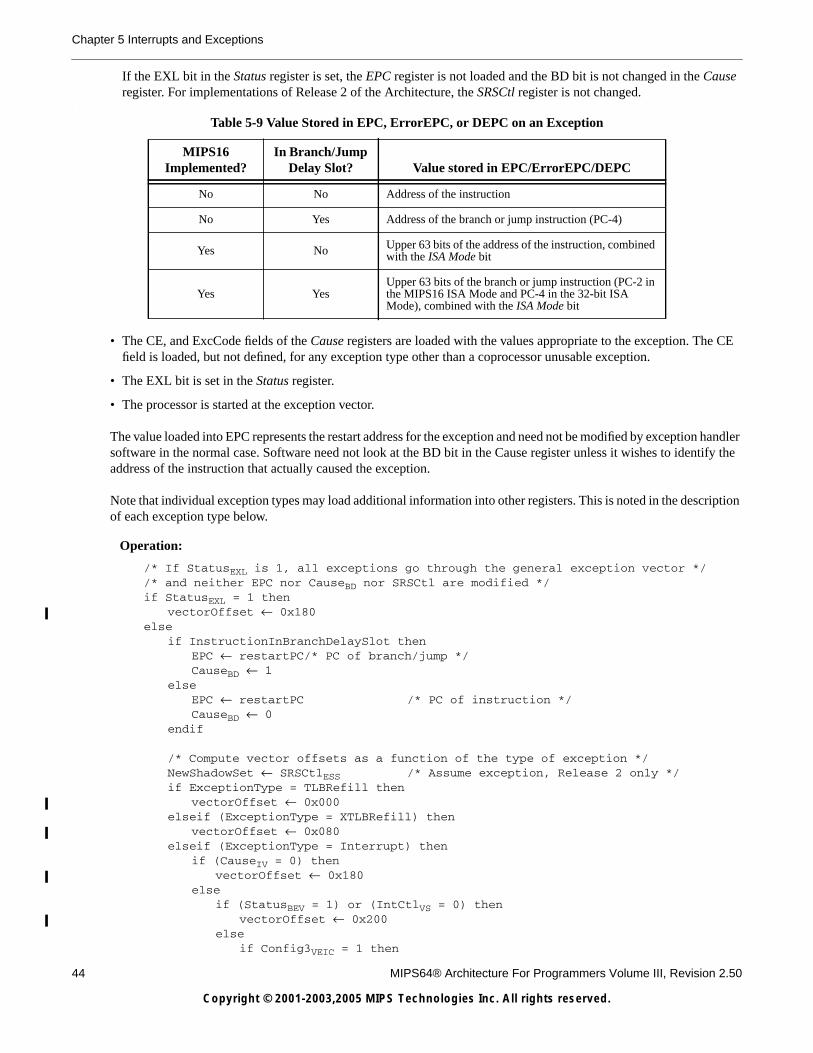
44 MIPS64® Architecture For Programmers Volume III, Revision 2.50
Copyright © 2001-2003,2005 MIPS Technologies Inc. All rights reserved.
Chapter 5 Interrupts and Exceptions
If the EXL bit in the Status register is set, the EPC register is not loaded and the BD bit is not changed in the Causeregister. For implementations of Release 2 of the Architecture, the SRSCtl register is not changed.
.
• The CE, and ExcCode fields of the Cause registers are loaded with the values appropriate to the exception. The CEfield is loaded, but not defined, for any exception type other than a coprocessor unusable exception.
• The EXL bit is set in the Status register.
• The processor is started at the exception vector.
The value loaded into EPC represents the restart address for the exception and need not be modified by exception handlersoftware in the normal case. Software need not look at the BD bit in the Cause register unless it wishes to identify theaddress of the instruction that actually caused the exception.
Note that individual exception types may load additional information into other registers. This is noted in the descriptionof each exception type below.
Operation:
/* If StatusEXL is 1, all exceptions go through the general exception vector *//* and neither EPC nor CauseBD nor SRSCtl are modified */if StatusEXL = 1 then
vectorOffset ← 0x180else
if InstructionInBranchDelaySlot thenEPC ← restartPC/* PC of branch/jump */CauseBD ← 1
elseEPC ← restartPC /* PC of instruction */CauseBD ← 0
endif
/* Compute vector offsets as a function of the type of exception */NewShadowSet ← SRSCtlESS /* Assume exception, Release 2 only */if ExceptionType = TLBRefill then
vectorOffset ← 0x000elseif (ExceptionType = XTLBRefill) then
vectorOffset ← 0x080elseif (ExceptionType = Interrupt) then
if (CauseIV = 0) thenvectorOffset ← 0x180
elseif (StatusBEV = 1) or (IntCtlVS = 0) then
vectorOffset ← 0x200else
if Config3VEIC = 1 then
Table 5-9 Value Stored in EPC, ErrorEPC, or DEPC on an Exception
MIPS16Implemented?
In Branch/JumpDelay Slot? Value stored in EPC/ErrorEPC/DEPC
No No Address of the instruction
No Yes Address of the branch or jump instruction (PC-4)
Yes No Upper 63 bits of the address of the instruction, combinedwith the ISA Mode bit
Yes YesUpper 63 bits of the branch or jump instruction (PC-2 inthe MIPS16 ISA Mode and PC-4 in the 32-bit ISAMode), combined with the ISA Mode bit
5.2 Exceptions
MIPS64® Architecture For Programmers Volume III, Revision 2.50 45
Copyright © 2001-2003,2005 MIPS Technologies Inc. All rights reserved.
VecNum ← CauseRIPLNewShadowSet ← SRSCtlEICSS
elseVecNum ← VIntPriorityEncoder()NewShadowSet ← SRSMapIPL×4+3..IPL×4
endifvectorOffset ← 0x200 + (VecNum × (IntCtlVS || 0b00000))
endif /* if (StatusBEV = 1) or (IntCtlVS = 0) then */endif /* if (CauseIV = 0) then */
endif /* elseif (ExceptionType = Interrupt) then */
/* Update the shadow set information for an implementation of *//* Release 2 of the architecture */if (ArchitectureRevision ≥ 2) and (SRSCtlHSS > 0) and (StatusBEV = 0) then
SRSCtlPSS ← SRSCtlCSSSRSCtlCSS ← NewShadowSet
endifendif /* if StatusEXL = 1 then */
CauseCE ← FaultingCoprocessorNumberCauseExcCode ← ExceptionTypeStatusEXL ← 1
/* Calculate the vector base address */if StatusBEV = 1 then
vectorBase ← 0xFFFF.FFFF.BFC0.0200else
if ArchitectureRevision ≥ 2 then/* The fixed value of EBase31..30 forces the base to be in kseg0 or kseg1 */vectorBase ← 0xFFFF.FFFF || EBase31..12 || 0x000
elsevectorBase ← 0xFFFF.FFFF.8000.0000
endifendif
/* Exception PC is the sum of vectorBase and vectorOffset. Vector *//* offsets > 0xFFF (vectored or EIC interrupts only), require *//* that EBase15..12 have zeros in each bit position less than or *//* equal to the most significant bit position of the vector offset */PC ← vectorBase63..30 || (vectorBase29..0 + vectorOffset29..0)
/* No carry between bits 29 and 30 */
5.2.3 EJTAG Debug Exception
An EJTAG Debug Exception occurs when one of a number of EJTAG-related conditions is met. Refer to the EJTAGSpecification for details of this exception.
Entry Vector Used
0xFFFF FFFF BFC0 0480 if the ProbTrap bit is zero in the EJTAG_Control_register; 0xFFFF FFFF FF200200 if the ProbTrap bit is one.
5.2.4 Reset Exception
A Reset Exception occurs when the Cold Reset signal is asserted to the processor. This exception is not maskable. Whena Reset Exception occurs, the processor performs a full reset initialization, including aborting state machines,
46 MIPS64® Architecture For Programmers Volume III, Revision 2.50
Copyright © 2001-2003,2005 MIPS Technologies Inc. All rights reserved.
Chapter 5 Interrupts and Exceptions
establishing critical state, and generally placing the processor in a state in which it can execute instructions fromuncached, unmapped address space. On a Reset Exception, only the following registers have defined state:
• The Random register is initialized to the number of TLB entries - 1.
• The Wired register is initialized to zero.
• The Config, Config1, Config2, and Config3 registers are initialized with their boot state.
• The RP, BEV, TS, SR, NMI, and ERL fields of the Status register are initialized to a specified state.
• Watch register enables and Performance Counter register interrupt enables are cleared.
• The ErrorEPC register is loaded with the restart PC, as described in Table 5-9. Note that this value may or may notbe predictable if the Reset Exception was taken as the result of power being applied to the processor because PC maynot have a valid value in that case. In some implementations, the value loaded into ErrorEPC register may not bepredictable on either a Reset or Soft Reset Exception.
• PC is loaded with 0xFFFF FFFF BFC0 0000.
Cause Register ExcCode Value
None
Additional State Saved
None
Entry Vector Used
Reset (0xFFFF FFFF BFC0 0000)
Operation
Random ← TLBEntries - 1EntryLo0PFNX ← 0 # Large physical address implementedEntryLo1PFNX ← 0 # Large physical address implementedPageMaskMaskX ← 0 # 1KB page support implementedPageGrainELPA ← 0 # Large physical address implementedPageGrainESP ← 0 # 1KB page support implementedWired ← 0HWREna← 0EntryHiVPN2X ← 0 # 1KB page support implementedStatusRP ← 0StatusBEV ← 1StatusTS ← 0StatusSR ← 0StatusNMI ← 0StatusERL ← 1IntCtlVS ← 0SRSCtlHSS ← HighestImplementedShadowSetSRSCtlESS ← 0SRSCtlPSS ← 0SRSCtlCSS ← 0SRSMap ← 0CauseDC ← 0EBaseExceptionBase ← 0Config ← ConfigurationStateConfigK0 ← 2 # Suggested - see Config register descriptionConfig1 ← ConfigurationStateConfig2 ← ConfigurationStateConfig3 ← ConfigurationStateWatchLo[n]I ← 0 # For all implemented Watch registersWatchLo[n]R ← 0 # For all implemented Watch registers
5.2 Exceptions
MIPS64® Architecture For Programmers Volume III, Revision 2.50 47
Copyright © 2001-2003,2005 MIPS Technologies Inc. All rights reserved.
WatchLo[n]W ← 0 # For all implemented Watch registersPerfCnt.Control[n]IE ← 0 # For all implemented PerfCnt registersif InstructionInBranchDelaySlot then
ErrorEPC ← restartPC # PC of branch/jumpelse
ErrorEPC ← restartPC # PC of instructionendifPC ← 0xFFFF FFFF BFC0 0000
5.2.5 Soft Reset Exception
A Soft Reset Exception occurs when the Reset signal is asserted to the processor. This exception is not maskable. Whena Soft Reset Exception occurs, the processor performs a subset of the full reset initialization. Although a Soft ResetException does not unnecessarily change the state of the processor, it may be forced to do so in order to place theprocessor in a state in which it can execute instructions from uncached, unmapped address space. Since bus, cache, orother operations may be interrupted, portions of the cache, memory, or other processor state may be inconsistent.
The primary difference between the Reset and Soft Reset Exceptions is in actual use. The Reset Exception is typicallyused to initialize the processor on power-up, while the Soft Reset Exception is typically used to recover from anon-responsive (hung) processor. The semantic difference is provided to allow boot software to save critical coprocessor0 or other register state to assist in debugging the potential problem. As such, the processor may reset the same statewhen either reset signal is asserted, but the interpretation of any state saved by software may be very different.
In addition to any hardware initialization required, the following state is established on a Soft Reset Exception:
• The RP, BEV, TS, SR, NMI, and ERL fields of the Status register are initialized to a specified state.
• Watch register enables and Performance Counter register interrupt enables are cleared.
• The ErrorEPC register is loaded with the restart PC, as described in Table 5-9. Note that this value may or may notbe predictable.
• PC is loaded with 0xFFFF FFFF BFC0 0000.
Cause Register ExcCode Value
None
Additional State Saved
None
Entry Vector Used
Reset (0xFFFF FFFF BFC0 0000)
Operation
EntryLo0PFNX ← 0 # Large physical address implementedEntryLo1PFNX ← 0 # Large physical address implementedPageMaskMaskX ← 0 # 1KB page support implementedPageGrainELPA ← 0 # Large physical address implementedPageGrainESP ← 0 # 1KB page support implementedEntryHiVPN2X ← 0 # 1KB page support implementedConfigK0 ← 2 # Suggested - see Config register descriptionStatusRP ← 0StatusBEV ← 1StatusTS ← 0StatusSR ← 1StatusNMI ← 0StatusERL ← 1
48 MIPS64® Architecture For Programmers Volume III, Revision 2.50
Copyright © 2001-2003,2005 MIPS Technologies Inc. All rights reserved.
Chapter 5 Interrupts and Exceptions
WatchLo[n]I ← 0 # For all implemented Watch registersWatchLo[n]R ← 0 # For all implemented Watch registersWatchLo[n]W ← 0 # For all implemented Watch registersPerfCnt.Control[n]IE ← 0 # For all implemented PerfCnt registersif InstructionInBranchDelaySlot then
ErrorEPC ← restartPC # PC of branch/jumpelse
ErrorEPC ← restartPC # PC of instructionendifPC ← 0xFFFF FFFF BFC0 0000
5.2.6 Non Maskable Interrupt (NMI) Exception
A non maskable interrupt exception occurs when the NMI signal is asserted to the processor.
Although described as an interrupt, it is more correctly described as an exception because it is not maskable. An NMIoccurs only at instruction boundaries, so does not do any reset or other hardware initialization. The state of the cache,memory, and other processor state is consistent and all registers are preserved, with the following exceptions:
• The BEV, TS, SR, NMI, and ERL fields of the Status register are initialized to a specified state.
• The ErrorEPC register is loaded with restart PC, as described in Table 5-9.
• PC is loaded with 0xFFFF FFFF BFC0 0000.
Cause Register ExcCode Value
None
Additional State Saved
None
Entry Vector Used
Reset (0xFFFF FFFF BFC0 0000)
Operation
StatusBEV ← 1StatusTS ← 0StatusSR ← 0StatusNMI ← 1StatusERL ← 1if InstructionInBranchDelaySlot then
ErrorEPC ← restartPC # PC of branch/jumpelse
ErrorEPC ← restartPC # PC of instructionendifPC ← 0xFFFF FFFF BFC0 0000
5.2.7 Machine Check Exception
A machine check exception occurs when the processor detects an internal inconsistency.
The following conditions cause a machine check exception:
• Detection of multiple matching entries in the TLB in a TLB-based MMU.
5.2 Exceptions
MIPS64® Architecture For Programmers Volume III, Revision 2.50 49
Copyright © 2001-2003,2005 MIPS Technologies Inc. All rights reserved.
Cause Register ExcCode Value
MCheck (See Table 8-25 on page 108)
Additional State Saved
Depends on the condition that caused the exception. See the descriptions above.
Entry Vector Used
General exception vector (offset 0x180)
5.2.8 Address Error Exception
An address error exception occurs under the following circumstances:
• A load or store doubleword instruction is executed in which the address is not aligned on a doubleword boundary.
• An instruction is fetched from an address that is not aligned on a word boundary.
• A load or store word instruction is executed in which the address is not aligned on a word boundary.
• A load or store halfword instruction is executed in which the address is not aligned on a halfword boundary.
• A reference is made to a kernel address space from User Mode or Supervisor Mode.
• A reference is made to a supervisor address space from User Mode.
• A reference is made to a a 64-bit address that is outside the range of the 32-bit Compatibility Address Space when64-bit address references are not enabled.
• A reference is made to an undefined or unimplemented 64-bit address when 64-bit address references are enabled.
Note that in the case of an instruction fetch that is not aligned on a word boundary, the PC is updated before the conditionis detected. Therefore, both EPC and BadVAddr point at the unaligned instruction address.
Cause Register ExcCode Value
AdEL: Reference was a load or an instruction fetch
AdES: Reference was a store
See Table 8-25 on page 108.
Additional State Saved
Entry Vector Used
General exception vector (offset 0x180)
Register State Value
BadVAddr failing address
ContextVPN2 UNPREDICTABLE
XContextVPN2 XContextR UNPREDICTABLE
EntryHiVPN2
EntryHiRUNPREDICTABLE
EntryLo0 UNPREDICTABLE
EntryLo1 UNPREDICTABLE
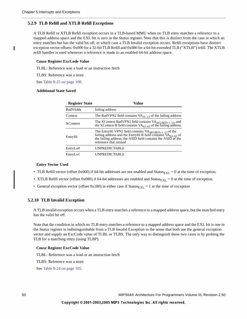
50 MIPS64® Architecture For Programmers Volume III, Revision 2.50
Copyright © 2001-2003,2005 MIPS Technologies Inc. All rights reserved.
Chapter 5 Interrupts and Exceptions
5.2.9 TLB Refill and XTLB Refill Exceptions
A TLB Refill or XTLB Refill exception occurs in a TLB-based MMU when no TLB entry matches a reference to amapped address space and the EXL bit is zero in the Status register. Note that this is distinct from the case in which anentry matches but has the valid bit off, in which case a TLB Invalid exception occurs. Refill exceptions have distinctexception vector offsets: 0x000 for a 32-bit TLB Refill and 0x080 for a 64-bit extended TLB (“XTLB”) refill. The XTLBrefill handler is used whenever a reference is made to an enabled 64-bit address space.
Cause Register ExcCode Value
TLBL: Reference was a load or an instruction fetch
TLBS: Reference was a store
See Table 8-25 on page 108.
Additional State Saved
Entry Vector Used
• TLB Refill vector (offset 0x000) if 64-bit addresses are not enabled and StatusEXL = 0 at the time of exception.
• XTLB Refill vector (offset 0x080) if 64-bit addresses are enabled and StatusEXL = 0 at the time of exception.
• General exception vector (offset 0x180) in either case if StatusEXL = 1 at the time of exception
5.2.10 TLB Invalid Exception
A TLB invalid exception occurs when a TLB entry matches a reference to a mapped address space, but the matched entryhas the valid bit off.
Note that the condition in which no TLB entry matches a reference to a mapped address space and the EXL bit is one inthe Status register is indistinguishable from a TLB Invalid Exception in the sense that both use the general exceptionvector and supply an ExcCode value of TLBL or TLBS. The only way to distinguish these two cases is by probing theTLB for a matching entry (using TLBP).
Cause Register ExcCode Value
TLBL: Reference was a load or an instruction fetch
TLBS: Reference was a store
See Table 8-24 on page 105.
Register State Value
BadVAddr failing address
Context The BadVPN2 field contains VA31..13 of the failing address
XContext The XContext BadVPN2 field contains VASEGBITS-1..13, andthe XContext R field contains VA63..62 of the failing address.
EntryHi
The EntryHi VPN2 field contains VASEGBITS-1..13 of thefailing address and the EntryHi R field contains VA63..62 ofthe failing address; the ASID field contains the ASID of thereference that missed
EntryLo0 UNPREDICTABLE
EntryLo1 UNPREDICTABLE
5.2 Exceptions
MIPS64® Architecture For Programmers Volume III, Revision 2.50 51
Copyright © 2001-2003,2005 MIPS Technologies Inc. All rights reserved.
Additional State Saved
Entry Vector Used
General exception vector (offset 0x180)
5.2.11 TLB Modified Exception
A TLB modified exception occurs on a store reference to a mapped address when the matching TLB entry is valid, butthe entry’s D bit is zero, indicating that the page is not writable.
Cause Register ExcCode Value
Mod (See Table 8-24 on page 105)
Additional State Saved
Entry Vector Used
General exception vector (offset 0x180)
5.2.12 Cache Error Exception
A cache error exception occurs when an instruction or data reference detects a cache tag or data error, or a parity or ECCerror is detected on the system bus when a cache miss occurs. This exception is not maskable. Because the error was ina cache, the exception vector is to an unmapped, uncached address.
Cause Register ExcCode Value
N/A
Register State Value
BadVAddr failing address
Context The BadVPN2 field contains VA31..13 of the failing address
XContext The XContext BadVPN2 field contains VASEGBITS-1..13, andthe XContext R field contains VA63..62 of the failing address.
EntryHi
The EntryHi VPN2 field contains VASEGBITS-1..13 of thefailing address and the EntryHi R field contains VA63..62 ofthe failing address; the ASID field contains the ASID of thereference that missed
EntryLo0 UNPREDICTABLE
EntryLo1 UNPREDICTABLE

52 MIPS64® Architecture For Programmers Volume III, Revision 2.50
Copyright © 2001-2003,2005 MIPS Technologies Inc. All rights reserved.
Chapter 5 Interrupts and Exceptions
Additional State Saved
Entry Vector Used
Cache error vector (offset 0x100)
Operation
CacheErr ← ErrorStateStatusERL ← 1if InstructionInBranchDelaySlot then
ErrorEPC ← restartPC # PC of branch/jumpelse
ErrorEPC ← restartPC # PC of instructionendifif StatusBEV = 1 then
PC ← 0xFFFF FFFF BFC0 0200 + 0x100else
if ArchitectureRevision ≥ 2 then/* The fixed value of EBase31..30 and bit 29 forced to a 1 puts the *//* vector in kseg1 */PC ← 0xFFFF.FFFF || EBase31..30 || 1 || EBase28..12 || 0x100
elsePC ← 0xFFFF FFFF A000 0000 + 0x100
endifendif
5.2.13 Bus Error Exception
A bus error occurs when an instruction, data, or prefetch access makes a bus request (due to a cache miss or anuncacheable reference) and that request is terminated in an error. Note that parity errors detected during bus transactionsare reported as cache error exceptions, not bus error exceptions.
Cause Register ExcCode Value
IBE: Error on an instruction reference
DBE: Error on a data reference
See Table 8-25 on page 108.
Additional State Saved
None
Entry Vector Used
General exception vector (offset 0x180)
5.2.14 Integer Overflow Exception
An integer overflow exception occurs when selected integer instructions result in a 2’s complement overflow.
Register State Value
CacheErr Error state
ErrorEPC Restart PC
5.2 Exceptions
MIPS64® Architecture For Programmers Volume III, Revision 2.50 53
Copyright © 2001-2003,2005 MIPS Technologies Inc. All rights reserved.
Cause Register ExcCode Value
Ov (See Table 8-25 on page 108)
Additional State Saved
None
Entry Vector Used
General exception vector (offset 0x180)
5.2.15 Trap Exception
A trap exception occurs when a trap instruction results in a TRUE value.
Cause Register ExcCode Value
Tr (See Table 8-25 on page 108)
Additional State Saved
None
Entry Vector Used
General exception vector (offset 0x180)
5.2.16 System Call Exception
A system call exception occurs when a SYSCALL instruction is executed.
Cause Register ExcCode Value
Sys (See Table 8-24 on page 105)
Additional State Saved
None
Entry Vector Used
General exception vector (offset 0x180)
5.2.17 Breakpoint Exception
A breakpoint exception occurs when a BREAK instruction is executed.
Cause Register ExcCode Value
Bp (See Table 8-25 on page 108)
Additional State Saved
None
Entry Vector Used
General exception vector (offset 0x180)
54 MIPS64® Architecture For Programmers Volume III, Revision 2.50
Copyright © 2001-2003,2005 MIPS Technologies Inc. All rights reserved.
Chapter 5 Interrupts and Exceptions
5.2.18 Reserved Instruction Exception
A Reserved Instruction Exception occurs if any of the following conditions is true:
• An instruction was executed that specifies an encoding of the opcode field that is flagged with “∗” (reserved), “β”(higher-order ISA), “⊥” (64-bit) if 64-bit operations are not enabled, or an unimplemented “ε” (ASE).
• An instruction was executed that specifies a SPECIAL opcode encoding of the function field that is flagged with “∗”(reserved), “β” (higher-order ISA), or “⊥” (64-bit) if 64-bit operations are not enabled.
• An instruction was executed that specifies a REGIMM opcode encoding of the rt field that is flagged with “∗”(reserved).
• An instruction was executed that specifies an unimplemented SPECIAL2 opcode encoding of the function field thatis flagged with an unimplemented “θ” (partner available), “⊥” (64-bit) if 64-bit operations are not enabled, or anunimplemented “σ” (EJTAG).
• An instruction was executed that specifies a COPz opcode encoding of the rs field that is flagged with “∗” (reserved),“β” (higher-order ISA), “⊥” (64-bit) if 64-bit operations are not enabled, or an unimplemented “ε” (ASE), assumingthat access to the coprocessor is allowed. If access to the coprocessor is not allowed, a Coprocessor UnusableException occurs instead. For the COP1 opcode, some implementations of previous ISAs reported this case as aFloating Point Exception, setting the Unimplemented Operation bit in the Cause field of the FCSR register.
• An instruction was executed that specifies an unimplemented COP0 opcode encoding of the function field when rs isCO that is flagged with “∗” (reserved), or an unimplemented “σ” (EJTAG), assuming that access to coprocessor 0 isallowed. If access to the coprocessor is not allowed, a Coprocessor Unusable Exception occurs instead.
• An instruction was executed that specifies a COP1 opcode encoding of the function field when rs is S, D, or W that isflagged with “∗” (reserved), “β” (higher-order ISA), “⊥” (64-bit) if 64-bit operations are not enabled, or anunimplemented “ε” (ASE), assuming that access to coprocessor 1 is allowed. If access to the coprocessor is notallowed, a Coprocessor Unusable Exception occurs instead. Some implementations of previous ISAs reported thiscase as a Floating Point Exception, setting the Unimplemented Operation bit in the Cause field of the FCSR register.
• An instruction was executed that specifies a COP1 opcode encoding when rs is L or PS and 64-bit operations are notenabled, or with a function field encoding that is flagged with “∗” (reserved), “β” (higher-order ISA), or anunimplemented “ε” (ASE), assuming that access to coprocessor 1 is allowed. If access to the coprocessor is notallowed, a Coprocessor Unusable Exception occurs instead. Some implementations of previous ISAs reported thiscase as a Floating Point Exception, setting the Unimplemented Operation bit in the Cause field of the FCSR register.
• An instruction was executed that specifies a COP1X opcode encoding of the function field that is flagged with “∗”(reserved), or any execution of the COP1X opcode when 64-bit operations are not enabled, assuming that access tocoprocessor 1 is allowed. If access to the coprocessor is not allowed, a Coprocessor Unusable Exception occursinstead. Some implementations of previous ISAs reported this case as a Floating Point Exception, setting theUnimplemented Operation bit in the Cause field of the FCSR register.
Cause Register ExcCode Value
RI (See Table 8-25 on page 108)
Additional State Saved
None
Entry Vector Used
General exception vector (offset 0x180)
5.2.19 Coprocessor Unusable Exception
A coprocessor unusable exception occurs if any of the following conditions is true:
5.2 Exceptions
MIPS64® Architecture For Programmers Volume III, Revision 2.50 55
Copyright © 2001-2003,2005 MIPS Technologies Inc. All rights reserved.
• A COP0 or Cache instruction was executed while the processor was running in a mode other than Debug Mode orKernel Mode, and the CU0 bit in the Status register was a zero
• A COP1, COP1X, LWC1, SWC1, LDC1, SDC1 or MOVCI (Special opcode function field encoding) instruction wasexecuted and the CU1 bit in the Status register was a zero.
• A COP2, LWC2, SWC2, LDC2, or SDC2 instruction was executed, and the CU2 bit in the Status register was a zero.
Cause Register ExcCode Value
CpU (See Table 8-24 on page 105)
Additional State Saved
Entry Vector Used
General exception vector (offset 0x180)
5.2.20 MDMX Unusable Exception
An MDMX unusable exception occurs if the MDMX instruction is executed and the MX bit of the Status register is a 0.Such an exception is used by the operating system to save and restore the state of the MDMX accumulator on a contextswitch (analogous to the save and restore of the FPRs).
Register ExcCode Value
MDMX (See Table 8-24 on page 105)
Additional State Saved
None
Entry Vector Used
General exception vector (offset 0x180)
5.2.21 Floating Point Exception
A floating point exception is initiated by the floating point coprocessor to signal a floating point exception.
Register ExcCode Value
FPE (See Table 8-24 on page 105)
Additional State Saved
Entry Vector Used
General exception vector (offset 0x180)
Register State Value
CauseCE unit number of the coprocessor being referenced
Register State Value
FCSR indicates the cause of the floating point exception
56 MIPS64® Architecture For Programmers Volume III, Revision 2.50
Copyright © 2001-2003,2005 MIPS Technologies Inc. All rights reserved.
Chapter 5 Interrupts and Exceptions
5.2.22 Coprocessor 2 Exception
A coprocessor 2 exception is initiated by coprocessor 2 to signal a precise coprocessor 2 exception.
Register ExcCode Value
C2E (See Table 8-24 on page 105)
Additional State Saved
Defined by the coprocessor
Entry Vector Used
General exception vector (offset 0x180)
5.2.23 Watch Exception
The watch facility provides a software debugging vehicle by initiating a watch exception when an instruction or datareference matches the address information stored in the WatchHi and WatchLo registers. A watch exception is takenimmediately if the EXL and ERL bits of the Status register are both zero. If either bit is a one at the time that a watchexception would normally be taken, the WP bit in the Cause register is set, and the exception is deferred until both theEXL and ERL bits in the Status register are zero. Software may use the WP bit in the Cause register to determine if theEPC register points at the instruction that caused the watch exception, or if the exception actually occurred while inkernel mode.
If the EXL or ERL bits are one in the Status register and a single instruction generates both a watch exception (which isdeferred by the state of the EXL and ERL bits) and a lower-priority exception, the lower priority exception is taken.
Watch exceptions are never taken if the processor is executing in Debug Mode. Should a watch register match while theprocessor is in Debug Mode, the exception is inhibited and the WP bit is not changed.
It is implementation dependent whether a data watch exception is triggered by a prefetch or cache instruction whoseaddress matches the Watch register address match conditions. A watch triggered by a SC or SCD instruction does soeven if the store would not complete because the LLbit is zero.
Register ExcCode Value
WATCH (See Table 8-24 on page 105)
Additional State Saved
Entry Vector Used
General exception vector (offset 0x180)
5.2.24 Interrupt Exception
The interrupt exception occurs when an enabled request for interrupt service is made. See Section 5.1 on page 31 formore information.
Register State Value
CauseWP
indicates that the watch exception was deferred until afterboth StatusEXL and StatusERL were zero. This bit directlycauses a watch exception, so software must clear this bit aspart of the exception handler to prevent a watch exceptionloop at the end of the current handler execution.
5.2 Exceptions
MIPS64® Architecture For Programmers Volume III, Revision 2.50 57
Copyright © 2001-2003,2005 MIPS Technologies Inc. All rights reserved.
Register ExcCode Value
Int (See Table 8-25 on page 108)
Additional State Saved
Entry Vector Used
General exception vector (offset 0x180) if the IV bit in the Cause register is zero.
Interrupt vector (offset 0x200) if the IV bit in the Cause register is one.
Register State Value
CauseIP indicates the interrupts that are pending.
58 MIPS64® Architecture For Programmers Volume III, Revision 2.50
Copyright © 2001-2003,2005 MIPS Technologies Inc. All rights reserved.
Chapter 5 Interrupts and Exceptions
MIPS64® Architecture For Programmers Volume III, Revision 2.50 59
Copyright © 2001-2003,2005 MIPS Technologies Inc. All rights reserved.
Chapter 6
GPR Shadow Registers
The capability in this chapter is targeted at removing the need to save and restore GPRs on entry to high priorityinterrupts or exceptions, and to provide specified processor modes with the same capability. This is done by introducingmultiple copies of the GPRs, called shadow sets, and allowing privileged software to associate a shadow set with entryto Kernel Mode via an interrupt vector or exception. The normal GPRs are logically considered shadow set zero.
The number of GPR shadow sets is implementation dependent and may range from one (the normal GPRs) to anarchitectural maximum of 16. The highest number actually implemented is indicated by the SRSCtlHSS field, and allshadow sets between 0 and SRSCtlHSS, inclusive must be implemented. If this field is zero, only the normal GPRs areimplemented.
6.1 Introduction to Shadow Sets
Shadow sets are new copies of the GPRs that can be substituted for the normal GPRs on entry to Kernel Mode via aninterrupt or exception. Once a shadow set is bound to a Kernel Mode entry condition, reference to GPRs work exactlyas one would expect, but they are redirected to registers that are dedicated to that condition. Privileged software mayneed to reference all GPRs in the register file, even specific shadow registers that are not visible in the current mode. TheRDPGPR and WRPGPR instructions are used for this purpose. The CSS field of the SRSCtl register provides the numberof the current shadow register set, and the PSS field of the SRSCtl register provides the number of the previous shadowregister set (that which was current before the last exception or interrupt occurred).
If the processor is operating in VI interrupt mode, binding of a vectored interrupt to a shadow set is done by writing tothe SRSMap register. If the processor is operating in EIC interrupt mode, the binding of the interrupt to a specific shadowset is provided by the external interrupt controller, and is configured in an implementation-dependent way. Binding ofan exception or non-vectored interrupt to a shadow set is done by writing to the ESS field of the SRSCtl register. Whenan exception or interrupt occurs, the value of SRSCtlCSS is copied to SRSCtlPSS, and SRSCtlCSS is set to the value takenfrom the appropriate source. On an ERET, the value of SRSCtlPSS is copied back into SRSCtlCSS to restore the shadowset of the mode to which control returns. More precisely, the rules for updating the fields in the SRSCtl register on aninterrupt or exception are as follows:
1. No field in the SRSCtl register is updated if any of the following conditions is true. In this case, steps 2 and 3 areskipped.
• The exception is one that sets StatusERL: NMI or cache error.
• The exception causes entry into EJTAG Debug Mode
• StatusBEV = 1
• StatusEXL = 1
2. SRSCtlCSS is copied to SRSCtlPSS
3. SRSCtlCSS is updated from one of the following sources:
• The appropriate field of the SRSMap register, based on IPL, if the exception is an interrupt, CauseIV = 1,Config3VEIC = 0, and Config3VInt = 1. These are the conditions for a vectored interrupt.
• The EICSS field of the SRSCtl register if the exception is an interrupt, CauseIV = 1 and Config3VEIC = 1. Theseare the conditions for a vectored EIC interrupt.
• The ESS field of the SRSCtl register in any other case. This is the condition for a non-interrupt exception, or anon-vectored interrupt.
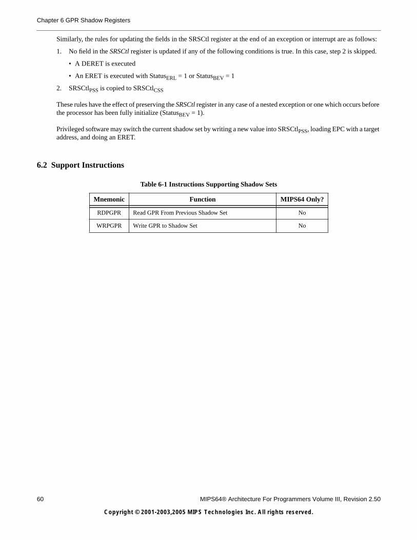
60 MIPS64® Architecture For Programmers Volume III, Revision 2.50
Copyright © 2001-2003,2005 MIPS Technologies Inc. All rights reserved.
Chapter 6 GPR Shadow Registers
Similarly, the rules for updating the fields in the SRSCtl register at the end of an exception or interrupt are as follows:
1. No field in the SRSCtl register is updated if any of the following conditions is true. In this case, step 2 is skipped.
• A DERET is executed
• An ERET is executed with StatusERL = 1 or StatusBEV = 1
2. SRSCtlPSS is copied to SRSCtlCSS
These rules have the effect of preserving the SRSCtl register in any case of a nested exception or one which occurs beforethe processor has been fully initialize (StatusBEV = 1).
Privileged software may switch the current shadow set by writing a new value into SRSCtlPSS, loading EPC with a targetaddress, and doing an ERET.
6.2 Support Instructions
Table 6-1 Instructions Supporting Shadow Sets
Mnemonic Function MIPS64 Only?
RDPGPR Read GPR From Previous Shadow Set No
WRPGPR Write GPR to Shadow Set No
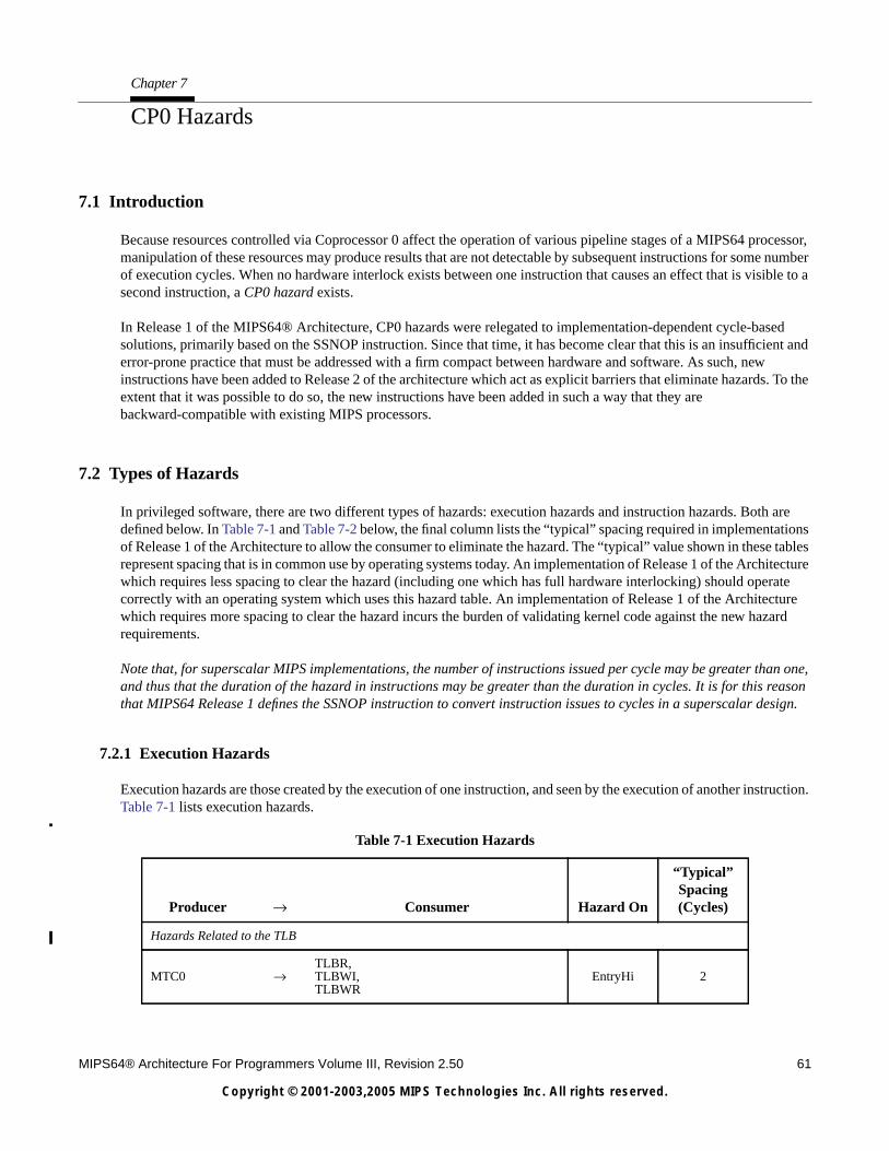
MIPS64® Architecture For Programmers Volume III, Revision 2.50 61
Copyright © 2001-2003,2005 MIPS Technologies Inc. All rights reserved.
Chapter 7
CP0 Hazards
7.1 Introduction
Because resources controlled via Coprocessor 0 affect the operation of various pipeline stages of a MIPS64 processor,manipulation of these resources may produce results that are not detectable by subsequent instructions for some numberof execution cycles. When no hardware interlock exists between one instruction that causes an effect that is visible to asecond instruction, a CP0 hazard exists.
In Release 1 of the MIPS64® Architecture, CP0 hazards were relegated to implementation-dependent cycle-basedsolutions, primarily based on the SSNOP instruction. Since that time, it has become clear that this is an insufficient anderror-prone practice that must be addressed with a firm compact between hardware and software. As such, newinstructions have been added to Release 2 of the architecture which act as explicit barriers that eliminate hazards. To theextent that it was possible to do so, the new instructions have been added in such a way that they arebackward-compatible with existing MIPS processors.
7.2 Types of Hazards
In privileged software, there are two different types of hazards: execution hazards and instruction hazards. Both aredefined below. In Table 7-1 and Table 7-2 below, the final column lists the “typical” spacing required in implementationsof Release 1 of the Architecture to allow the consumer to eliminate the hazard. The “typical” value shown in these tablesrepresent spacing that is in common use by operating systems today. An implementation of Release 1 of the Architecturewhich requires less spacing to clear the hazard (including one which has full hardware interlocking) should operatecorrectly with an operating system which uses this hazard table. An implementation of Release 1 of the Architecturewhich requires more spacing to clear the hazard incurs the burden of validating kernel code against the new hazardrequirements.
Note that, for superscalar MIPS implementations, the number of instructions issued per cycle may be greater than one,and thus that the duration of the hazard in instructions may be greater than the duration in cycles. It is for this reasonthat MIPS64 Release 1 defines the SSNOP instruction to convert instruction issues to cycles in a superscalar design.
7.2.1 Execution Hazards
Execution hazards are those created by the execution of one instruction, and seen by the execution of another instruction.Table 7-1 lists execution hazards.
Table 7-1 Execution Hazards
Producer → Consumer Hazard On
“Typical”Spacing(Cycles)
Hazards Related to the TLB
MTC0 →TLBR,TLBWI,TLBWR
EntryHi 2
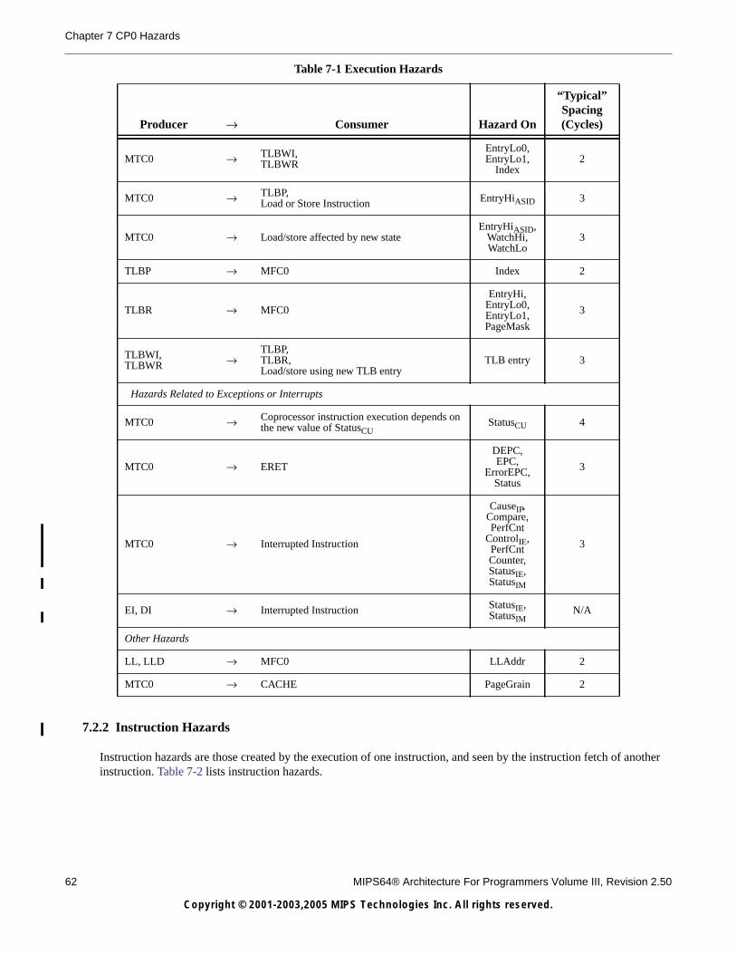
62 MIPS64® Architecture For Programmers Volume III, Revision 2.50
Copyright © 2001-2003,2005 MIPS Technologies Inc. All rights reserved.
Chapter 7 CP0 Hazards
7.2.2 Instruction Hazards
Instruction hazards are those created by the execution of one instruction, and seen by the instruction fetch of anotherinstruction. Table 7-2 lists instruction hazards.
MTC0 → TLBWI,TLBWR
EntryLo0,EntryLo1,
Index2
MTC0 → TLBP,Load or Store Instruction EntryHiASID 3
MTC0 → Load/store affected by new stateEntryHiASID,
WatchHi,WatchLo
3
TLBP → MFC0 Index 2
TLBR → MFC0
EntryHi,EntryLo0,EntryLo1,PageMask
3
TLBWI,TLBWR →
TLBP,TLBR,Load/store using new TLB entry
TLB entry 3
Hazards Related to Exceptions or Interrupts
MTC0 → Coprocessor instruction execution depends onthe new value of StatusCU
StatusCU 4
MTC0 → ERET
DEPC,EPC,
ErrorEPC,Status
3
MTC0 → Interrupted Instruction
CauseIP,Compare,PerfCnt
ControlIE,PerfCntCounter,StatusIE,StatusIM
3
EI, DI → Interrupted Instruction StatusIE,StatusIM
N/A
Other Hazards
LL, LLD → MFC0 LLAddr 2
MTC0 → CACHE PageGrain 2
Table 7-1 Execution Hazards
Producer → Consumer Hazard On
“Typical”Spacing(Cycles)
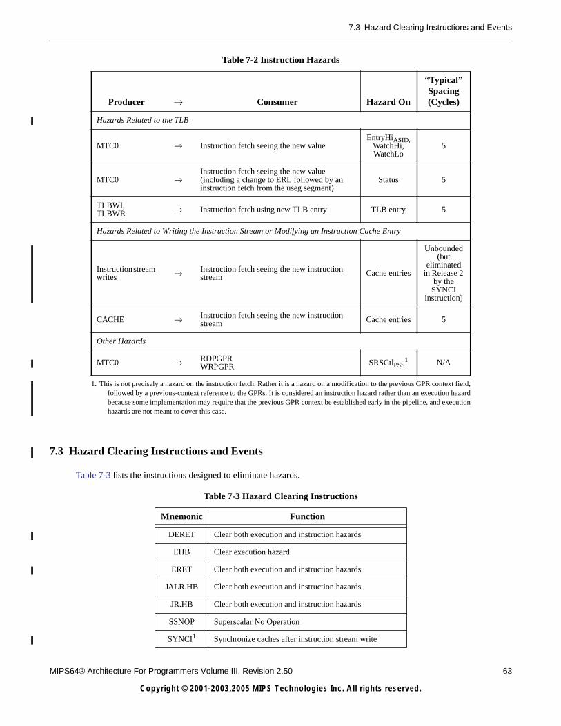
7.3 Hazard Clearing Instructions and Events
MIPS64® Architecture For Programmers Volume III, Revision 2.50 63
Copyright © 2001-2003,2005 MIPS Technologies Inc. All rights reserved.
7.3 Hazard Clearing Instructions and Events
Table 7-3 lists the instructions designed to eliminate hazards.
Table 7-2 Instruction Hazards
Producer → Consumer Hazard On
“Typical”Spacing(Cycles)
Hazards Related to the TLB
MTC0 → Instruction fetch seeing the new valueEntryHiASID,
WatchHi,WatchLo
5
MTC0 →Instruction fetch seeing the new value(including a change to ERL followed by aninstruction fetch from the useg segment)
Status 5
TLBWI,TLBWR → Instruction fetch using new TLB entry TLB entry 5
Hazards Related to Writing the Instruction Stream or Modifying an Instruction Cache Entry
Instructionstreamwrites → Instruction fetch seeing the new instruction
stream Cache entries
Unbounded(but
eliminatedin Release 2
by theSYNCI
instruction)
CACHE → Instruction fetch seeing the new instructionstream Cache entries 5
Other Hazards
MTC0 → RDPGPRWRPGPR SRSCtlPSS
1
1. This is not precisely a hazard on the instruction fetch. Rather it is a hazard on a modification to the previous GPR context field,followed by a previous-context reference to the GPRs. It is considered an instruction hazard rather than an execution hazardbecause some implementation may require that the previous GPR context be established early in the pipeline, and executionhazards are not meant to cover this case.
N/A
Table 7-3 Hazard Clearing Instructions
Mnemonic Function
DERET Clear both execution and instruction hazards
EHB Clear execution hazard
ERET Clear both execution and instruction hazards
JALR.HB Clear both execution and instruction hazards
JR.HB Clear both execution and instruction hazards
SSNOP Superscalar No Operation
SYNCI1 Synchronize caches after instruction stream write
64 MIPS64® Architecture For Programmers Volume III, Revision 2.50
Copyright © 2001-2003,2005 MIPS Technologies Inc. All rights reserved.
Chapter 7 CP0 Hazards
DERET, ERET, and SSNOP are available in Release 1 of the Architecture; EHB, JALR.HB, JR.HB, and SYNCI wereadded in Release 2 of the Architecture. In both Release 1 and Release 2 of the Architecture, DERET and ERET clearboth execution and instruction hazards and they are the only timing-independent instructions which will do this in bothreleases of the architecture.
Even though DERET and ERET clear hazards between the execution of the instruction and the target instruction stream,an execution hazard may still be created between a write of the DEPC, EPC, ErrorEPC, or Status registers and theDERET or ERET instruction.
In addition, an exception or interrupt also clears both execution and instruction hazards between the instruction thatcreated the hazard and the first instruction of the exception or interrupt handler. Said another way, no hazards remainvisible by the first instruction of an exception or interrupt handler.
7.3.1 Instruction Encoding
The EHB instruction is encoded using a variant of the NOP/SSNOP encoding. This encoding was chosen forcompatibility with the Release 1 SSNOP instruction, such that existing software may be modified to be compatible withboth Release 1 and Release 2 implementations. See the EHB instruction description for additional information.
The JALR.HB and JR.HB instructions are encoding using bit 10 of the hint field of the JALR and JR instructions. Theseencodings were chosen for compatibility with existing MIPS implementations, including many which pre-date theMIPS64 architecture. Because a pipeline flush clears hazards on most early implementations, the JALR.HB or JR.HBinstructions can be included in existing software for backward and forward compatibility. See the JALR.HB and JR.HBinstructions for additional information.
The SYNCI instruction is encoded using a new encoding of the REGIMM opcode. This encoding was chosen becauseit causes a Reserved Instruction exception on all Release 1 implementations. As such, kernel software running onprocessors that don’t implement Release 2 can emulate the function using the CACHE instruction.
1. SYNCI synchronizes caches after an instruction stream write, and before executionof that instruction stream. As such, it is not precisely a coprocessor 0 hazard, butis included here for completeness.
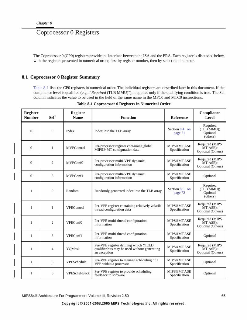
MIPS64® Architecture For Programmers Volume III, Revision 2.50 65
Copyright © 2001-2003,2005 MIPS Technologies Inc. All rights reserved.
Chapter 8
Coprocessor 0 Registers
The Coprocessor 0 (CP0) registers provide the interface between the ISA and the PRA. Each register is discussed below,with the registers presented in numerical order, first by register number, then by select field number.
8.1 Coprocessor 0 Register Summary
Table 8-1 lists the CP0 registers in numerical order. The individual registers are described later in this document. If thecompliance level is qualified (e.g., “Required (TLB MMU)”), it applies only if the qualifying condition is true. The Selcolumn indicates the value to be used in the field of the same name in the MFC0 and MTC0 instructions.
Table 8-1 Coprocessor 0 Registers in Numerical Order
RegisterNumber Sel1
RegisterName Function Reference
ComplianceLevel
0 0 Index Index into the TLB array Section 8.4 onpage 71
Required(TLB MMU);
Optional(others)
0 1 MVPControl Per-processor register containing globalMIPS® MT configuration data
MIPS®MTASESpecification
Required (MIPSMT ASE);
Optional (Others)
0 2 MVPConf0 Per-processor multi-VPE dynamicconfiguration information
MIPS®MTASESpecification
Required (MIPSMT ASE);
Optional (Others)
0 3 MVPConf1 Per-processor multi-VPE dynamicconfiguration information
MIPS®MTASESpecification Optional
1 0 Random Randomly generated index into the TLB array Section 8.5 onpage 72
Required(TLB MMU);
Optional(others)
1 1 VPEControl Per-VPE register containing relatively volatilethread configuration data
MIPS®MTASESpecification
Required (MIPSMT ASE);
Optional (Others)
1 2 VPEConf0 Per-VPE multi-thread configurationinformation
MIPS®MTASESpecification
Required (MIPSMT ASE);
Optional (Others)
1 3 VPEConf1 Per-VPE multi-thread configurationinformation
MIPS®MTASESpecification Optional
1 4 YQMaskPer-VPE register defining which YIELDqualifier bits may be used without generatingan exception
MIPS®MTASESpecification
Required (MIPSMT ASE);
Optional (Others)
1 5 VPESchedule Per-VPE register to manage scheduling of aVPE within a processor
MIPS®MTASESpecification Optional
1 6 VPEScheFBack Per-VPE register to provide schedulingfeedback to software
MIPS®MTASESpecification Optional
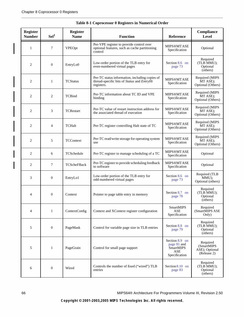
66 MIPS64® Architecture For Programmers Volume III, Revision 2.50
Copyright © 2001-2003,2005 MIPS Technologies Inc. All rights reserved.
Chapter 8 Coprocessor 0 Registers
1 7 VPEOptPer-VPE register to provide control overoptional features, such as cache partitioningcontrol
MIPS®MTASESpecification Optional
2 0 EntryLo0 Low-order portion of the TLB entry foreven-numbered virtual pages
Section 8.6 onpage 73
Required(TLB MMU);
Optional(others)
2 1 TCStatusPer-TC status information, including copies ofthread-specific bits of Status and EntryHiregisters.
MIPS®MTASESpecification
Required (MIPSMT ASE);
Optional (Others)
2 2 TCBind Per-TC information about TC ID and VPEbinding
MIPS®MTASESpecification
Required (MIPSMT ASE);
Optional (Others)
2 3 TCRestart Per-TC value of restart instruction address forthe associated thread of execution
MIPS®MTASESpecification
Required (MIPSMT ASE);
Optional (Others)
2 4 TCHalt Per-TC register controlling Halt state of TC MIPS®MTASESpecification
Required (MIPSMT ASE);
Optional (Others)
2 5 TCContext Per-TC read/write storage for operating systemuse
MIPS®MTASESpecification
Required (MIPSMT ASE);
Optional (Others)
2 6 TCSchedule Per-TC register to manage scheduling of a TC MIPS®MTASESpecification Optional
2 7 TCScheFBack Per-TC register to provide scheduling feedbackto software
MIPS®MTASESpecification Optional
3 0 EntryLo1 Low-order portion of the TLB entry forodd-numbered virtual pages
Section 8.6 onpage 73
Required (TLBMMU);
Optional (others)
4 0 Context Pointer to page table entry in memory Section 8.7 onpage 78
Required(TLB MMU);
Optional(others)
4 1 ContextConfig Context and XContext register configuration SmartMIPS
ASESpecification
Required(SmartMIPS ASE
Only)
5 0 PageMask Control for variable page size in TLB entries Section 8.8 onpage 79
Required(TLB MMU);
Optional(others)
5 1 PageGrain Control for small page support
Section 8.9 onpage 81 andSmartMIPS
ASESpecification
Required(SmartMIPS
ASE); Optional(Release 2)
6 0 Wired Controls the number of fixed (“wired”) TLBentries
Section 8.10 onpage 83
Required(TLB MMU);
Optional(others)
Table 8-1 Coprocessor 0 Registers in Numerical Order
RegisterNumber Sel1
RegisterName Function Reference
ComplianceLevel
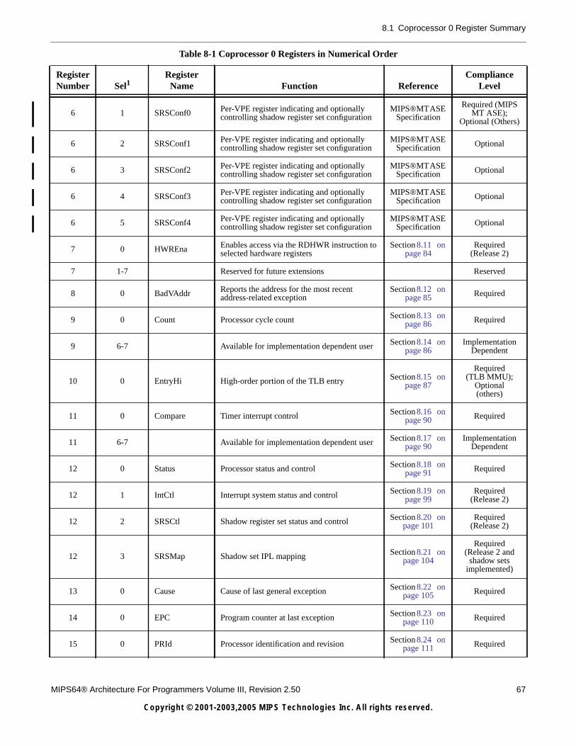
8.1 Coprocessor 0 Register Summary
MIPS64® Architecture For Programmers Volume III, Revision 2.50 67
Copyright © 2001-2003,2005 MIPS Technologies Inc. All rights reserved.
6 1 SRSConf0 Per-VPE register indicating and optionallycontrolling shadow register set configuration
MIPS®MTASESpecification
Required (MIPSMT ASE);
Optional (Others)
6 2 SRSConf1 Per-VPE register indicating and optionallycontrolling shadow register set configuration
MIPS®MTASESpecification Optional
6 3 SRSConf2 Per-VPE register indicating and optionallycontrolling shadow register set configuration
MIPS®MTASESpecification Optional
6 4 SRSConf3 Per-VPE register indicating and optionallycontrolling shadow register set configuration
MIPS®MTASESpecification Optional
6 5 SRSConf4 Per-VPE register indicating and optionallycontrolling shadow register set configuration
MIPS®MTASESpecification Optional
7 0 HWREna Enables access via the RDHWR instruction toselected hardware registers
Section 8.11 onpage 84
Required(Release 2)
7 1-7 Reserved for future extensions Reserved
8 0 BadVAddr Reports the address for the most recentaddress-related exception
Section 8.12 onpage 85 Required
9 0 Count Processor cycle count Section 8.13 onpage 86 Required
9 6-7 Available for implementation dependent user Section 8.14 onpage 86
ImplementationDependent
10 0 EntryHi High-order portion of the TLB entry Section 8.15 onpage 87
Required(TLB MMU);
Optional(others)
11 0 Compare Timer interrupt control Section 8.16 onpage 90 Required
11 6-7 Available for implementation dependent user Section 8.17 onpage 90
ImplementationDependent
12 0 Status Processor status and control Section 8.18 onpage 91 Required
12 1 IntCtl Interrupt system status and control Section 8.19 onpage 99
Required(Release 2)
12 2 SRSCtl Shadow register set status and control Section 8.20 onpage 101
Required(Release 2)
12 3 SRSMap Shadow set IPL mapping Section 8.21 onpage 104
Required(Release 2 and
shadow setsimplemented)
13 0 Cause Cause of last general exception Section 8.22 onpage 105 Required
14 0 EPC Program counter at last exception Section 8.23 onpage 110 Required
15 0 PRId Processor identification and revision Section 8.24 onpage 111 Required
Table 8-1 Coprocessor 0 Registers in Numerical Order
RegisterNumber Sel1
RegisterName Function Reference
ComplianceLevel
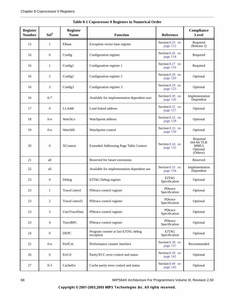
68 MIPS64® Architecture For Programmers Volume III, Revision 2.50
Copyright © 2001-2003,2005 MIPS Technologies Inc. All rights reserved.
Chapter 8 Coprocessor 0 Registers
15 1 EBase Exception vector base register Section 8.25 onpage 112
Required(Release 2)
16 0 Config Configuration register Section 8.26 onpage 114 Required
16 1 Config1 Configuration register 1 Section 8.27 onpage 116 Required
16 2 Config2 Configuration register 2 Section 8.28 onpage 120 Optional
16 3 Config3 Configuration register 3 Section 8.29 onpage 123 Optional
16 6-7 Available for implementation dependent user Section 8.30 onpage 126
ImplementationDependent
17 0 LLAddr Load linked address Section 8.31 onpage 127 Optional
18 0-n WatchLo Watchpoint address Section 8.32 onpage 128 Optional
19 0-n WatchHi Watchpoint control Section 8.33 onpage 130 Optional
20 0 XContext Extended Addressing Page Table Context Section 8.34 onpage 132
Required(64-bit TLB
MMU)Optional(Others)
21 all Reserved for future extensions Reserved
22 all Available for implementation dependent use Section 8.35 onpage 134
ImplementationDependent
23 0 Debug EJTAG Debug register EJTAGSpecification Optional
23 1 TraceControl PDtrace control register PDtraceSpecification Optional
23 2 TraceControl2 PDtrace control register PDtraceSpecification Optional
23 3 UserTraceData PDtrace control register PDtraceSpecification Optional
23 4 TraceBPC PDtrace control register PDtraceSpecification Optional
24 0 DEPC Program counter at last EJTAG debugexception
EJTAGSpecification Optional
25 0-n PerfCnt Performance counter interface Section 8.38 onpage 137 Recommended
26 0 ErrCtl Parity/ECC error control and status Section 8.39 onpage 141 Optional
27 0-3 CacheErr Cache parity error control and status Section 8.40 onpage 142 Optional
Table 8-1 Coprocessor 0 Registers in Numerical Order
RegisterNumber Sel1
RegisterName Function Reference
ComplianceLevel

8.2 Notation
MIPS64® Architecture For Programmers Volume III, Revision 2.50 69
Copyright © 2001-2003,2005 MIPS Technologies Inc. All rights reserved.
8.2 Notation
For each register described below, field descriptions include the read/write properties of the field, and the reset state ofthe field. For the read/write properties of the field, the following notation is used:
28 even selects TagLo Low-order portion of cache tag interface Section 8.41 onpage 143 Required (Cache)
28 odd selects DataLo Low-order portion of cache data interface Section 8.42 onpage 144 Optional
29 even selects TagHi High-order portion of cache tag interface Section 8.43 onpage 145 Required (Cache)
29 odd selects DataHi High-order portion of cache data interface Section 8.44 onpage 146 Optional
30 0 ErrorEPC Program counter at last error Section 8.45 onpage 147 Required
31 0 DESAVE EJTAG debug exception save register EJTAGSpecification Optional
1. Any select (Sel) value not explicitly noted as available for implementation-dependent use is reserved for future use by the Architecture.
Table 8-2 Read/Write Bit Field Notation
Read/WriteNotation Hardware Interpretation Software Interpretation
R/W
A field in which all bits are readable and writable by software and, potentially, by hardware.
Hardware updates of this field are visible by software read. Software updates of this field arevisible by hardware read.
If the Reset State of this field is “Undefined”, either software or hardware must initialize the valuebefore the first read will return a predictable value. This should not be confused with the formaldefinition of UNDEFINED behavior.
R
A field which is either static or is updated onlyby hardware.
If the Reset State of this field is either “0”,“Preset”, or “Externally Set”, hardwareinitializes this field to zero or to the appropriatestate, respectively, on powerup. The term“Preset” is used to suggest that the processorestablishes the appropriate state, whereas theterm “Externally Set” is used to suggest that thestate is established via an external source (e.g.,personality pins or initialization bit stream).These terms are suggestions only, and are notintended to act as a requirement on theimplementation.
If the Reset State of this field is “Undefined”,hardware updates this field only under thoseconditions specified in the description of thefield.
A field to which the value written by softwareis ignored by hardware. Software may writeany value to this field without affectinghardware behavior. Software reads of this fieldreturn the last value updated by hardware.
If the Reset State of this field is “Undefined”,software reads of this field result in anUNPREDICTABLE value except after ahardware update done under the conditionsspecified in the description of the field.
Table 8-1 Coprocessor 0 Registers in Numerical Order
RegisterNumber Sel1
RegisterName Function Reference
ComplianceLevel
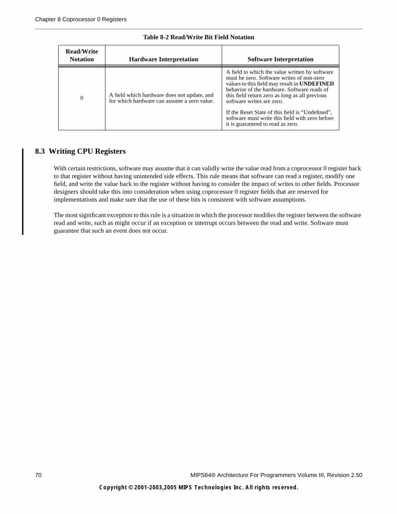
70 MIPS64® Architecture For Programmers Volume III, Revision 2.50
Copyright © 2001-2003,2005 MIPS Technologies Inc. All rights reserved.
Chapter 8 Coprocessor 0 Registers
8.3 Writing CPU Registers
With certain restrictions, software may assume that it can validly write the value read from a coprocessor 0 register backto that register without having unintended side effects. This rule means that software can read a register, modify onefield, and write the value back to the register without having to consider the impact of writes to other fields. Processordesigners should take this into consideration when using coprocessor 0 register fields that are reserved forimplementations and make sure that the use of these bits is consistent with software assumptions.
The most significant exception to this rule is a situation in which the processor modifies the register between the softwareread and write, such as might occur if an exception or interrupt occurs between the read and write. Software mustguarantee that such an event does not occur.
0 A field which hardware does not update, andfor which hardware can assume a zero value.
A field to which the value written by softwaremust be zero. Software writes of non-zerovalues to this field may result in UNDEFINEDbehavior of the hardware. Software reads ofthis field return zero as long as all previoussoftware writes are zero.
If the Reset State of this field is “Undefined”,software must write this field with zero beforeit is guaranteed to read as zero.
Table 8-2 Read/Write Bit Field Notation
Read/WriteNotation Hardware Interpretation Software Interpretation
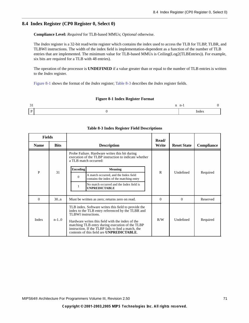
8.4 Index Register (CP0 Register 0, Select 0)
MIPS64® Architecture For Programmers Volume III, Revision 2.50 71
Copyright © 2001-2003,2005 MIPS Technologies Inc. All rights reserved.
8.4 Index Register (CP0 Register 0, Select 0)
Compliance Level: Required for TLB-based MMUs; Optional otherwise.
The Index register is a 32-bit read/write register which contains the index used to access the TLB for TLBP, TLBR, andTLBWI instructions. The width of the index field is implementation-dependent as a function of the number of TLBentries that are implemented. The minimum value for TLB-based MMUs is Ceiling(Log2(TLBEntries)). For example,six bits are required for a TLB with 48 entries).
The operation of the processor is UNDEFINED if a value greater than or equal to the number of TLB entries is writtento the Index register.
Figure 8-1 shows the format of the Index register; Table 8-3 describes the Index register fields.
Figure 8-1 Index Register Format
31 n n-1 0
P 0 Index
Table 8-3 Index Register Field Descriptions
Fields
DescriptionRead/Write Reset State ComplianceName Bits
P 31
Probe Failure. Hardware writes this bit duringexecution of the TLBP instruction to indicate whethera TLB match occurred:
R Undefined Required
0 30..n Must be written as zero; returns zero on read. 0 0 Reserved
Index n-1..0
TLB index. Software writes this field to provide theindex to the TLB entry referenced by the TLBR andTLBWI instructions.
Hardware writes this field with the index of thematching TLB entry during execution of the TLBPinstruction. If the TLBP fails to find a match, thecontents of this field are UNPREDICTABLE.
R/W Undefined Required
Encoding Meaning
0A match occurred, and the Index fieldcontains the index of the matching entry
1No match occurred and the Index field isUNPREDICTABLE
72 MIPS64® Architecture For Programmers Volume III, Revision 2.50
Copyright © 2001-2003,2005 MIPS Technologies Inc. All rights reserved.
8.5 Random Register (CP0 Register 1, Select 0)
Compliance Level: Required for TLB-based MMUs; Optional otherwise.
The Random register is a read-only register whose value is used to index the TLB during a TLBWR instruction. Thewidth of the Random field is calculated in the same manner as that described for the Index register above.
The value of the register varies between an upper and lower bound as follow:
• A lower bound is set by the number of TLB entries reserved for exclusive use by the operating system (the contentsof the Wired register). The entry indexed by the Wired register is the first entry available to be written by a TLBWrite Random operation.
• An upper bound is set by the total number of TLB entries minus 1.
Within the required constraints of the upper and lower bounds, the manner in which the processor selects values for theRandom register is implementation-dependent.
The processor initializes the Random register to the upper bound on a Reset Exception, and when the Wired register iswritten.
Figure 8-2 shows the format of the Random register; Table 8-4 describes the Random register fields.
Figure 8-2 Random Register Format
31 n n-1 0
0 Random
Table 8-4 Random Register Field Descriptions
Fields
DescriptionRead/Write Reset State ComplianceName Bits
0 31..n Must be written as zero; returns zero on read. 0 0 Reserved
Random n-1..0 TLB Random Index R TLB Entries - 1 Required
8.6 EntryLo0, EntryLo1 (CP0 Registers 2 and 3, Select 0)
MIPS64® Architecture For Programmers Volume III, Revision 2.50 73
Copyright © 2001-2003,2005 MIPS Technologies Inc. All rights reserved.
8.6 EntryLo0, EntryLo1 (CP0 Registers 2 and 3, Select 0)
Compliance Level: EntryLo0 is Required for a TLB-based MMU; Optional otherwise.
Compliance Level: EntryLo1 is Required for a TLB-based MMU; Optional otherwise.
The pair of EntryLo registers act as the interface between the TLB and the TLBP, TLBR, TLBWI, and TLBWRinstructions. EntryLo0 holds the entries for even pages and EntryLo1 holds the entries for odd pages.
Software may determine the value of PABITS by writing all ones to the EntryLo0 or EntryLo1 registers and reading thevalue back. Bits read as “1” from the PFN field allow software to determine the boundary between the PFN/PFNX andFillfields to calculate the value of PABITS.
The contents of the EntryLo0 and EntryLo1 registers are not defined after an address error exception and some fieldsmay be modified by hardware during the address error exception sequence. Software writes of the EntryHi register (viaMTC0 or DMTC0) do not cause the implicit update of address-related fields in the BadVAddr or Context registers.
For Release 1 of the Architecture, Figure 8-3 shows the format of the EntryLo0 and EntryLo1 registers; Table 8-5describes the EntryLo0 and EntryLo1 register fields. For Release 2 of the Architecture, Figure 8-4 shows the format ofthe EntryLo0 and EntryLo1 registers; Table 8-6 describes the EntryLo0 and EntryLo1 register fields.
Figure 8-3 EntryLo0, EntryLo1 Register Format in Release 1 of the Architecture
63 32
Fill
Fill PFN C D V G
31 30 29 6 5 3 2 1 0
Table 8-5 EntryLo0, EntryLo1 Register Field Descriptions in Release 1 of the Architecture
Fields
DescriptionRead/Write Reset State ComplianceName Bits
Fill 63..30These bits are ignored on write and return zero on read.The boundaries of this field change as a function of thevalue of PABITS. See Table 8-7 for more information.
R 0 Required
PFN 29..6
Page Frame Number. Corresponds to bits PABITS-1..12of the physical address, where PABITS is the width ofthe physical address in bits. The boundaries of this fieldchange as a function of the value of PABITS. See Table8-7 for more information.
R/W Undefined Required
C 5..3 Coherency attribute of the page. See Table 8-8 below. R/W Undefined Required
D 2
“Dirty” bit, indicating that the page is writable. If thisbit is a one, stores to the page are permitted. If this bitis a zero, stores to the page cause a TLB Modifiedexception.
Kernel software may use this bit to implement pagingalgorithms that require knowing which pages have beenwritten. If this bit is always zero when a page is initiallymapped, the TLB Modified exception that results onany store to the page can be used to update kernel datastructures that indicate that the page was actuallywritten.
R/W Undefined Required
74 MIPS64® Architecture For Programmers Volume III, Revision 2.50
Copyright © 2001-2003,2005 MIPS Technologies Inc. All rights reserved.
V 1
Valid bit, indicating that the TLB entry, and thus thevirtual page mapping are valid. If this bit is a one,accesses to the page are permitted. If this bit is a zero,accesses to the page cause a TLB Invalid exception.
R/W Undefined Required
G 0
Global bit. On a TLB write, the logical AND of the Gbits from both EntryLo0 and EntryLo1 becomes the Gbit in the TLB entry. If the TLB entry G bit is a one,ASID comparisons are ignored during TLB matches.On a read from a TLB entry, the G bits of bothEntryLo0 and EntryLo1 reflect the state of the TLB Gbit.
R/W Undefined Required(TLB MMU)
Figure 8-4 EntryLo0, EntryLo1 Register Format in Release 2 of the Architecture
63 55 54 32
Fill PFNX
PFNX PFN C D V G
31 30 29 6 5 3 2 1 0
Table 8-6 EntryLo0, EntryLo1 Register Field Descriptions in Release 2 of the Architecture
Fields
DescriptionRead/Write Reset State ComplianceName Bits
Fill 63..55These bits are ignored on write and return zero on read.The boundaries of this field change as a function of thevalue of PABITS. See Table 8-7 for more information.
R 0 Required
PFNX 54..30
Page Frame Number Extension. If the processor isenabled to support large physical addresses(Config3LPA = 1 and PageGrainELPA = 1), this field isconcatenated with the PFN field to form the full pageframe number corresponding to the physical address,thereby providing up to 59 bits of physical address.
If the processor is enabled to support 1KB pages(Config3SP = 1 and PageGrainESP = 1), the combinedPFNX || PFN fields corresponds to bits PABITS-1..10 ofthe physical address (the field is shifted left by 2 bitsrelative to the Release 1 definition to make room forPA11..10).
If the processor is not enabled to support 1KB pages(Config3SP = 0 or PageGrainESP = 0), the combinedPFNX || PFN fields corresponds to 0b00 || bitsPABITS-1..12 of the physical address (the field isunshifted and the upper two bits must be written aszero).
The boundaries of this field change as a function of thevalue of PABITS. See Table 8-7 for more information.
If support for large physical addresses is not enabled(Config3LPA = 0 or PageGrainELPA = 0), these bits areignored on write and return 0 on read, therebyproviding full backward compatibility withimplementations of Release 1 of the Architecture.
R/W 0 Optional
Table 8-5 EntryLo0, EntryLo1 Register Field Descriptions in Release 1 of the Architecture
Fields
DescriptionRead/Write Reset State ComplianceName Bits
8.6 EntryLo0, EntryLo1 (CP0 Registers 2 and 3, Select 0)
MIPS64® Architecture For Programmers Volume III, Revision 2.50 75
Copyright © 2001-2003,2005 MIPS Technologies Inc. All rights reserved.
Table 8-7 shows the movement of the Fill, PFNX, and PFN fields as a function of 1KB page support enabled, and thevalue of PABITS. Note that in implementations of Release 1 of the Architecture, PABITS can never be larger than 36 bitsand there is no support for 1KB pages, so only the second row of the table applies to Release 1.
PFN 29..6
Page Frame Number. This field containsleast-significant bits of the physical page numbercorresponding to the virtual page. If the processor isenabled to support large physical addresses, the PFNXfield, described above is concatenated with the PFNfield to form the full page frame number. If theprocessor is not enabled to support large physicaladdresses, the entire page frame number is representedby this field. See the description of the PFNX fieldabove for more information.
If the processor is enabled to support 1KB pages(Config3SP = 1 and PageGrainESP = 1), the PFN fieldcorresponds to bits 33..10 of the physical address (thefield is shifted left by 2 bits relative to the Release 1definition to make room for PA11..10).
If the processor is not enabled to support 1KB pages(Config3SP = 0 or PageGrainESP = 0), the PFN fieldcorresponds to bits 35..12 of the physical address.
The boundaries of this field change as a function of thevalue of PABITS. See Table 8-7 for more information.
R/W Undefined Required
C 5..3 The definition of this field is unchanged from Release1. See Table 8-5 above and Table 8-8 below. R/W Undefined Required
D 2 The definition of this field is unchanged from Release1. See Table 8-5 above. R/W Undefined Required
V 1 The definition of this field is unchanged from Release1. See Table 8-5 above. R/W Undefined Required
G 0 The definition of this field is unchanged from Release1. See Table 8-5 above. R/W Undefined Required
(TLB MMU)
Table 8-6 EntryLo0, EntryLo1 Register Field Descriptions in Release 2 of the Architecture
Fields
DescriptionRead/Write Reset State ComplianceName Bits
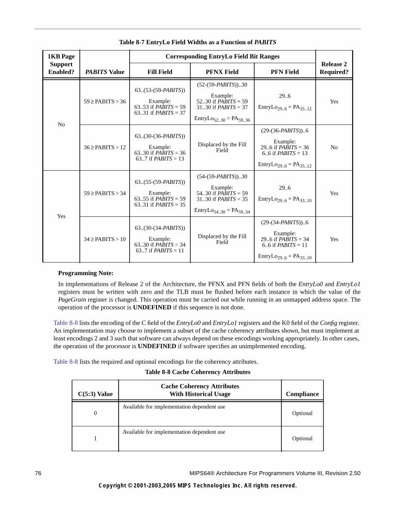
76 MIPS64® Architecture For Programmers Volume III, Revision 2.50
Copyright © 2001-2003,2005 MIPS Technologies Inc. All rights reserved.
Programming Note:
In implementations of Release 2 of the Architecture, the PFNX and PFN fields of both the EntryLo0 and EntryLo1registers must be written with zero and the TLB must be flushed before each instance in which the value of thePageGrain register is changed. This operation must be carried out while running in an unmapped address space. Theoperation of the processor is UNDEFINED if this sequence is not done.
Table 8-8 lists the encoding of the C field of the EntryLo0 and EntryLo1 registers and the K0 field of the Config register.An implementation may choose to implement a subset of the cache coherency attributes shown, but must implement atleast encodings 2 and 3 such that software can always depend on these encodings working appropriately. In other cases,the operation of the processor is UNDEFINED if software specifies an unimplemented encoding.
Table 8-8 lists the required and optional encodings for the coherency attributes.
Table 8-7 EntryLo Field Widths as a Function of PABITS
1KB PageSupport
Enabled? PABITS Value
Corresponding EntryLo Field Bit RangesRelease 2
Required?Fill Field PFNX Field PFN Field
No
59 ≥ PABITS > 36
63..(53-(59-PABITS))
Example:63..53 if PABITS = 5963..31 if PABITS = 37
(52-(59-PABITS))..30
Example:52..30 if PABITS = 5931..30 if PABITS = 37
EntryLo52..30 = PA59..36
29..6
EntryLo29..6 = PA35..12
Yes
36 ≥ PABITS > 12
63..(30-(36-PABITS))
Example:63..30 if PABITS = 3663..7 if PABITS = 13
Displaced by the FillField
(29-(36-PABITS))..6
Example:29..6 if PABITS = 366..6 if PABITS = 13
EntryLo29..6 = PA35..12
No
Yes
59 ≥ PABITS > 34
63..(55-(59-PABITS))
Example:63..55 if PABITS = 5963..31 if PABITS = 35
(54-(59-PABITS))..30
Example:54..30 if PABITS = 5931..30 if PABITS = 35
EntryLo54..30 = PA59..34
29..6
EntryLo29..6 = PA33..10
Yes
34 ≥ PABITS > 10
63..(30-(34-PABITS))
Example:63..30 if PABITS = 3463..7 if PABITS = 11
Displaced by the FillField
(29-(34-PABITS))..6
Example:29..6 if PABITS = 346..6 if PABITS = 11
EntryLo29..6 = PA33..10
Yes
Table 8-8 Cache Coherency Attributes
C(5:3) ValueCache Coherency Attributes
With Historical Usage Compliance
0Available for implementation dependent use
Optional
1Available for implementation dependent use
Optional
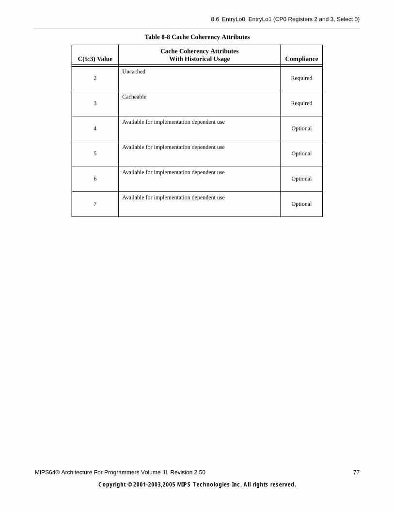
8.6 EntryLo0, EntryLo1 (CP0 Registers 2 and 3, Select 0)
MIPS64® Architecture For Programmers Volume III, Revision 2.50 77
Copyright © 2001-2003,2005 MIPS Technologies Inc. All rights reserved.
2Uncached
Required
3Cacheable
Required
4Available for implementation dependent use
Optional
5Available for implementation dependent use
Optional
6Available for implementation dependent use
Optional
7Available for implementation dependent use
Optional
Table 8-8 Cache Coherency Attributes
C(5:3) ValueCache Coherency Attributes
With Historical Usage Compliance

78 MIPS64® Architecture For Programmers Volume III, Revision 2.50
Copyright © 2001-2003,2005 MIPS Technologies Inc. All rights reserved.
8.7 Context Register (CP0 Register 4, Select 0)
Compliance Level: Required for TLB-based MMUs; Optional otherwise.
The Context register is a read/write register containing a pointer to an entry in the page table entry (PTE) array. Thisarray is an operating system data structure that stores virtual-to-physical translations. During a TLB miss, the operatingsystem loads the TLB with the missing translation from the PTE array. The Context register is primarily intended foruse with the TLB Refill handler, but is also loaded by hardware on an XTLB Refill and may be used by software in thathandler. The Context register duplicates some of the information provided in the BadVAddr register, but is organized insuch a way that the operating system can directly reference a 16-byte structure in memory that describes the mapping.
A TLB exception (TLB Refill, XTLB Refill, TLB Invalid, or TLB Modified) causes bits VA31..13 of the virtual addressto be written into the BadVPN2 field of the Context register. The PTEBase field is written and used by the operatingsystem.
The BadVPN2 field of the Context register is not defined after an address error exception and this field may be modifiedby hardware during the address error exception sequence.
Figure 8-5 shows the format of the Context Register; Table 8-9 describes the Context register fields.
Figure 8-5 Context Register Format
63 23 22 4 3 0
PTEBase BadVPN2 0
Table 8-9 Context Register Field Descriptions
Fields
DescriptionRead/Write Reset State ComplianceName Bits
PTEBase 63..23
This field is for use by the operating system and isnormally written with a value that allows theoperating system to use the Context Register as apointer into the current PTE array in memory.
R/W Undefined Required
BadVPN2 22..4This field is written by hardware on a TLBexception. It contains bits VA31..13 of the virtualaddress that caused the exception.
R Undefined Required
0 3..0 Must be written as zero; returns zero on read. 0 0 Reserved
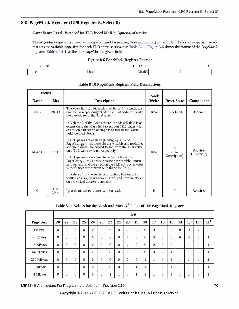
8.8 PageMask Register (CP0 Register 5, Select 0)
MIPS64® Architecture For Programmers Volume III, Revision 2.50 79
Copyright © 2001-2003,2005 MIPS Technologies Inc. All rights reserved.
8.8 PageMask Register (CP0 Register 5, Select 0)
Compliance Level: Required for TLB-based MMUs; Optional otherwise.
The PageMask register is a read/write register used for reading from and writing to the TLB. It holds a comparison maskthat sets the variable page size for each TLB entry, as shown in Table 8-11. Figure 8-6 shows the format of the PageMaskregister; Table 8-10 describes the PageMask register fields.
Figure 8-6 PageMask Register Format
31 29 28 13 12 11 0
0 Mask MaskX 0
Table 8-10 PageMask Register Field Descriptions
Fields
DescriptionRead/Write Reset State ComplianceName Bits
Mask 28..13The Mask field is a bit mask in which a “1” bit indicatesthat the corresponding bit of the virtual address shouldnot participate in the TLB match.
R/W Undefined Required
MaskX 12..11
In Release 2 of the Architecture, the MaskX field is anextension to the Mask field to support 1KB pages withdefinition and action analogous to that of the Maskfield, defined above.
If 1KB pages are enabled (Config3SP = 1 andPageGrainESP = 1), these bits are writable and readable,and their values are copied to and from the TLB entryon a TLB write or read, respectivly.
If 1KB pages are not enabled (Config3SP = 0 orPageGrainESP = 0), these bits are not writable, returnzero on read, and the effect on the TLB entry on a writeis as if they were written with the value 0b11.
In Release 1 of the Architecture, these bits must bewritten as zero, return zero on read, and have no effecton the virtual address translation.
R/W0
(SeeDescription)
Required(Release 2)
0 31..29,10..0 Ignored on write; returns zero on read. R 0 Required
Table 8-11 Values for the Mask and MaskX1 Fields of the PageMask Register
Page Size
Bit
28 27 26 25 24 23 22 21 20 19 18 17 16 15 14 13 121 111
1 KByte 0 0 0 0 0 0 0 0 0 0 0 0 0 0 0 0 0 0
4 KBytes 0 0 0 0 0 0 0 0 0 0 0 0 0 0 0 0 1 1
16 KBytes 0 0 0 0 0 0 0 0 0 0 0 0 0 0 1 1 1 1
64 KBytes 0 0 0 0 0 0 0 0 0 0 0 0 1 1 1 1 1 1
256 KBytes 0 0 0 0 0 0 0 0 0 0 1 1 1 1 1 1 1 1
1 MByte 0 0 0 0 0 0 0 0 1 1 1 1 1 1 1 1 1 1
4 MByte 0 0 0 0 0 0 1 1 1 1 1 1 1 1 1 1 1 1
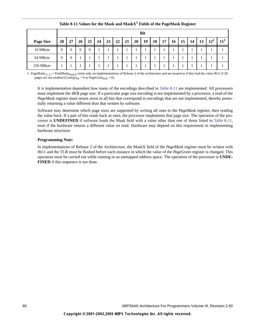
80 MIPS64® Architecture For Programmers Volume III, Revision 2.50
Copyright © 2001-2003,2005 MIPS Technologies Inc. All rights reserved.
It is implementation dependent how many of the encodings described in Table 8-11 are implemented. All processorsmust implement the 4KB page size. If a particular page size encoding is not implemented by a processor, a read of thePageMask register must return zeros in all bits that correspond to encodings that are not implemented, thereby poten-tially returning a value different than that written by software.
Software may determine which page sizes are supported by writing all ones to the PageMask register, then readingthe value back. If a pair of bits reads back as ones, the processor implements that page size. The operation of the pro-cessor is UNDEFINED if software loads the Mask field with a value other than one of those listed in Table 8-11,even if the hardware returns a different value on read. Hardware may depend on this requirement in implementinghardware structures
Programming Note:
In implementations of Release 2 of the Architecture, the MaskX field of the PageMask register must be written with0b11 and the TLB must be flushed before each instance in which the value of the PageGrain register is changed. Thisoperation must be carried out while running in an unmapped address space. The operation of the processor is UNDE-FINED if this sequence is not done.
16 MByte 0 0 0 0 1 1 1 1 1 1 1 1 1 1 1 1 1 1
64 MByte 0 0 1 1 1 1 1 1 1 1 1 1 1 1 1 1 1 1
256 MByte 1 1 1 1 1 1 1 1 1 1 1 1 1 1 1 1 1 1
1. PageMask12..11 = PaskMaskMaskX exists only on implementations of Release 2 of the architecture and are treated as if they had the value 0b11 if 1Kpages are not enabled (Config3SP = 0 or PageGrainESP = 0).
Table 8-11 Values for the Mask and MaskX1 Fields of the PageMask Register
Page Size
Bit
28 27 26 25 24 23 22 21 20 19 18 17 16 15 14 13 121 111

8.9 PageGrain Register (CP0 Register 5, Select 1)
MIPS64® Architecture For Programmers Volume III, Revision 2.50 81
Copyright © 2001-2003,2005 MIPS Technologies Inc. All rights reserved.
8.9 PageGrain Register (CP0 Register 5, Select 1)
Compliance Level: Required for implementations of Release 2 of the Architecture that include TLB-based MMUs andsupport 1KB pages, or large physical addresses; Optional otherwise.
The PageGrain register is a read/write register used for enabling 1KB page support, and large physical address support.The PageGrain register is present in both the SmartMIPS™ ASE, and in Release 2 of the Architecture, although thereare no bits in common between the two uses of this register. As such, the description below only describes the fieldsrelevant to Release 2 of the Architecture. In implementations of both Release 2 of the Architecture and the SmartMIPS™ASE, the ASE definitions take precedence and none of the Release 2 fields described below are present. Figure 8-7 showsthe format of the PageGrain register; Table 8-12 describes the PageGrain register fields.
Figure 8-7 PageGrain Register Format
31 30 29 28 27 13 12 8 7 0
ASE ELPA ESP 0 ASE 0
Table 8-12 PageGrain Register Field Descriptions
Fields
DescriptionRead/Write Reset State ComplianceName Bits
ASE 31..30,12..8
These fields are control features of the SmartMIPS™ASE and are not used in implementations of Release 2of the Architecture unless such an implementation alsoimplements the SmartMIPS™ ASE.
0 0 Required
ELPA 29
Enables support for large physical addresses.
If this bit is a 1, the following changes occur tocoprocessor 0 registers:• The PFNX field of the EntryLo0 and EntryLo1
registers is writable and concatenated with the PFNfield to form the full page frame number.
If Config3LPA = 0, large physical addresses are notimplemented, and this bit is ignored on write andreturns zero on read.
R/W 0 Required
Encoding Meaning
0Large physical address support is notenabled
1Large physical address support isenabled
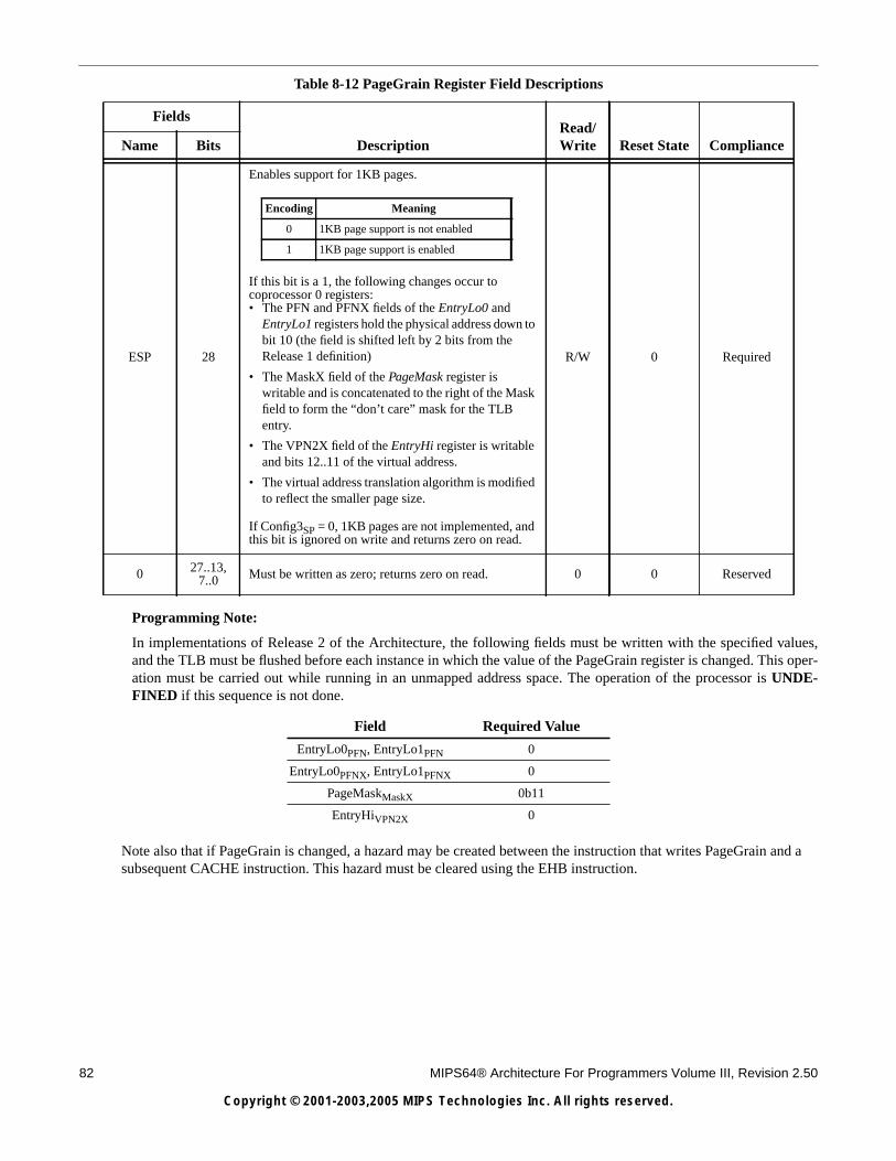
82 MIPS64® Architecture For Programmers Volume III, Revision 2.50
Copyright © 2001-2003,2005 MIPS Technologies Inc. All rights reserved.
Programming Note:
In implementations of Release 2 of the Architecture, the following fields must be written with the specified values,and the TLB must be flushed before each instance in which the value of the PageGrain register is changed. This oper-ation must be carried out while running in an unmapped address space. The operation of the processor is UNDE-FINED if this sequence is not done.
Note also that if PageGrain is changed, a hazard may be created between the instruction that writes PageGrain and asubsequent CACHE instruction. This hazard must be cleared using the EHB instruction.
ESP 28
Enables support for 1KB pages.
If this bit is a 1, the following changes occur tocoprocessor 0 registers:• The PFN and PFNX fields of the EntryLo0 and
EntryLo1 registers hold the physical address down tobit 10 (the field is shifted left by 2 bits from theRelease 1 definition)
• The MaskX field of the PageMask register iswritable and is concatenated to the right of the Maskfield to form the “don’t care” mask for the TLBentry.
• The VPN2X field of the EntryHi register is writableand bits 12..11 of the virtual address.
• The virtual address translation algorithm is modifiedto reflect the smaller page size.
If Config3SP = 0, 1KB pages are not implemented, andthis bit is ignored on write and returns zero on read.
R/W 0 Required
0 27..13,7..0 Must be written as zero; returns zero on read. 0 0 Reserved
Field Required Value
EntryLo0PFN, EntryLo1PFN 0
EntryLo0PFNX, EntryLo1PFNX 0
PageMaskMaskX 0b11
EntryHiVPN2X 0
Table 8-12 PageGrain Register Field Descriptions
Fields
DescriptionRead/Write Reset State ComplianceName Bits
Encoding Meaning
0 1KB page support is not enabled
1 1KB page support is enabled
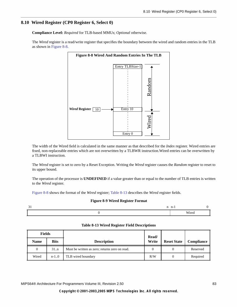
8.10 Wired Register (CP0 Register 6, Select 0)
MIPS64® Architecture For Programmers Volume III, Revision 2.50 83
Copyright © 2001-2003,2005 MIPS Technologies Inc. All rights reserved.
8.10 Wired Register (CP0 Register 6, Select 0)
Compliance Level: Required for TLB-based MMUs; Optional otherwise.
The Wired register is a read/write register that specifies the boundary between the wired and random entries in the TLBas shown in Figure 8-8.
The width of the Wired field is calculated in the same manner as that described for the Index register. Wired entries arefixed, non-replaceable entries which are not overwritten by a TLBWR instruction.Wired entries can be overwritten bya TLBWI instruction.
The Wired register is set to zero by a Reset Exception. Writing the Wired register causes the Random register to reset toits upper bound.
The operation of the processor is UNDEFINED if a value greater than or equal to the number of TLB entries is writtento the Wired register.
Figure 8-8 shows the format of the Wired register; Table 8-13 describes the Wired register fields.
Figure 8-9 Wired Register Format
31 n n-1 0
0 Wired
Table 8-13 Wired Register Field Descriptions
Fields
DescriptionRead/Write Reset State ComplianceName Bits
0 31..n Must be written as zero; returns zero on read. 0 0 Reserved
Wired n-1..0 TLB wired boundary R/W 0 Required
Ran
dom
Wir
ed
Entry 0
Entry 1010Wired Register
Figure 8-8 Wired And Random Entries In The TLB
Entry TLBSize-1
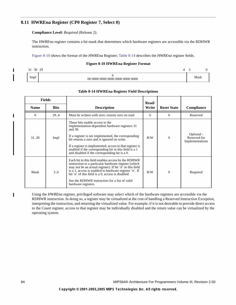
84 MIPS64® Architecture For Programmers Volume III, Revision 2.50
Copyright © 2001-2003,2005 MIPS Technologies Inc. All rights reserved.
8.11 HWREna Register (CP0 Register 7, Select 0)
Compliance Level: Required (Release 2).
The HWREna register contains a bit mask that determines which hardware registers are accessible via the RDHWRinstruction.
Figure 8-10 shows the format of the HWREna Register; Table 8-14 describes the HWREna register fields.
Using the HWREna register, privileged software may select which of the hardware registers are accessible via theRDHWR instruction. In doing so, a register may be virtualized at the cost of handling a Reserved Instruction Exception,interpreting the instruction, and returning the virtualized value. For example, if it is not desirable to provide direct accessto the Count register, access to that register may be individually disabled and the return value can be virtualized by theoperating system.
Figure 8-10 HWREna Register Format
31 30 29 4 3 0
Impl 000 0000 0000 0000 0000 0000 0000 Mask
Table 8-14 HWREna Register Field Descriptions
Fields
DescriptionRead/Write Reset State ComplianceName Bits
0 29..4 Must be written with zero; returns zero on read 0 0 Reserved
31..30 Impl
These bits enable access to theimplementation-dependent hardware registers 31and 30.
If a register is not implemented, the correspondingbit returns a zero and is ignored on write.
If a register is implemented, access to that register isenabled if the corresponding bit in this field is a 1and disabled if the corresponding bit is a 0.
R/W 0Optional -
Reserved forImplementations
Mask 3..0
Each bit in this field enables access by the RDHWRinstruction to a particular hardware register (whichmay not be an actual register). If bit ‘n’ in this fieldis a 1, access is enabled to hardware register ‘n’. Ifbit ‘n’ of this field is a 0, access is disabled.
See the RDHWR instruction for a list of validhardware registers.
R/W 0 Required
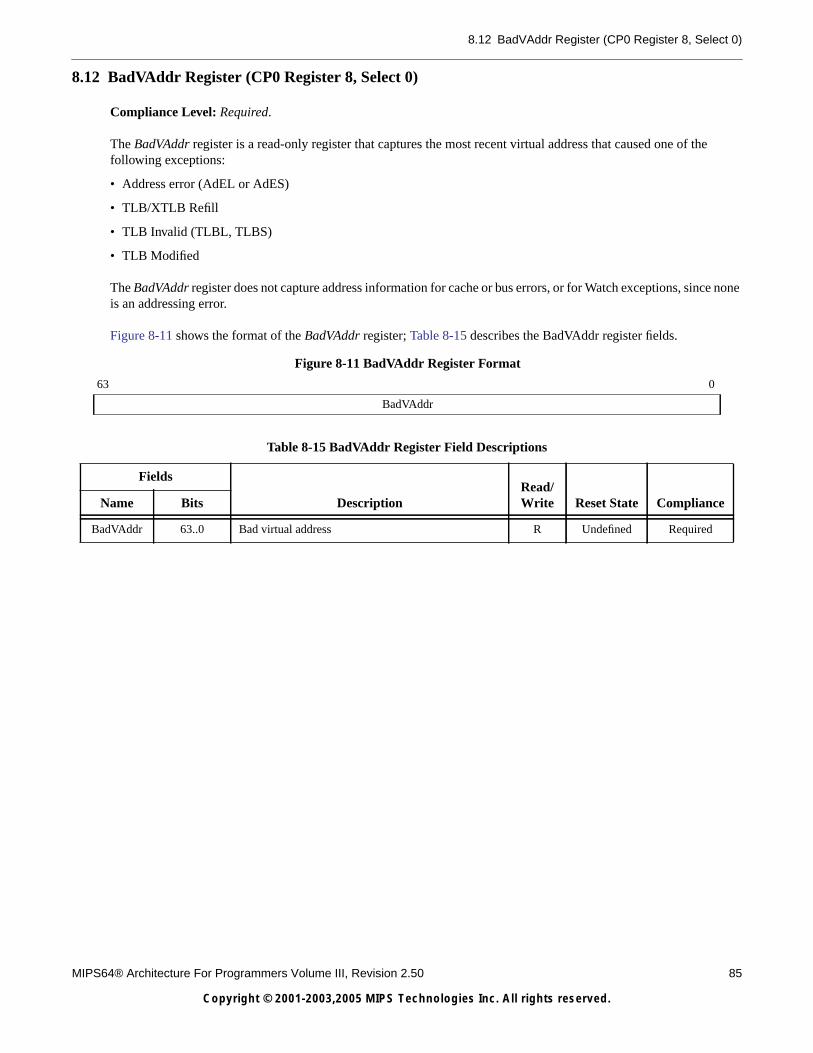
8.12 BadVAddr Register (CP0 Register 8, Select 0)
MIPS64® Architecture For Programmers Volume III, Revision 2.50 85
Copyright © 2001-2003,2005 MIPS Technologies Inc. All rights reserved.
8.12 BadVAddr Register (CP0 Register 8, Select 0)
Compliance Level: Required.
The BadVAddr register is a read-only register that captures the most recent virtual address that caused one of thefollowing exceptions:
• Address error (AdEL or AdES)
• TLB/XTLB Refill
• TLB Invalid (TLBL, TLBS)
• TLB Modified
The BadVAddr register does not capture address information for cache or bus errors, or for Watch exceptions, since noneis an addressing error.
Figure 8-11 shows the format of the BadVAddr register; Table 8-15 describes the BadVAddr register fields.
Figure 8-11 BadVAddr Register Format
63 0
BadVAddr
Table 8-15 BadVAddr Register Field Descriptions
Fields
DescriptionRead/Write Reset State ComplianceName Bits
BadVAddr 63..0 Bad virtual address R Undefined Required
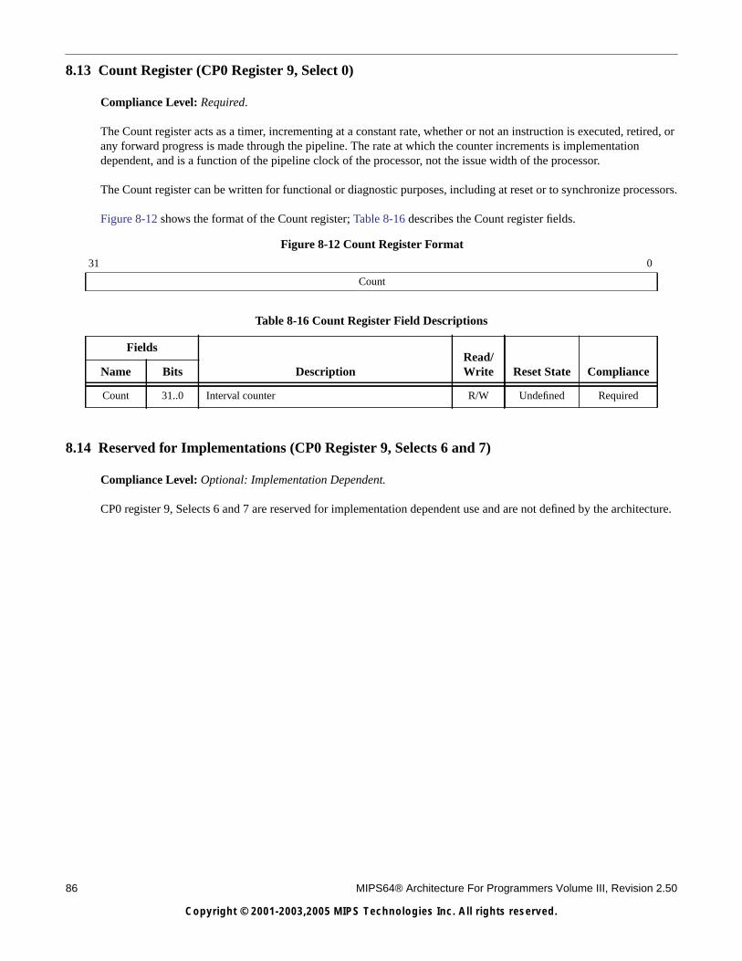
86 MIPS64® Architecture For Programmers Volume III, Revision 2.50
Copyright © 2001-2003,2005 MIPS Technologies Inc. All rights reserved.
8.13 Count Register (CP0 Register 9, Select 0)
Compliance Level: Required.
The Count register acts as a timer, incrementing at a constant rate, whether or not an instruction is executed, retired, orany forward progress is made through the pipeline. The rate at which the counter increments is implementationdependent, and is a function of the pipeline clock of the processor, not the issue width of the processor.
The Count register can be written for functional or diagnostic purposes, including at reset or to synchronize processors.
Figure 8-12 shows the format of the Count register; Table 8-16 describes the Count register fields.
8.14 Reserved for Implementations (CP0 Register 9, Selects 6 and 7)
Compliance Level: Optional: Implementation Dependent.
CP0 register 9, Selects 6 and 7 are reserved for implementation dependent use and are not defined by the architecture.
Figure 8-12 Count Register Format
31 0
Count
Table 8-16 Count Register Field Descriptions
Fields
DescriptionRead/Write Reset State ComplianceName Bits
Count 31..0 Interval counter R/W Undefined Required

8.15 EntryHi Register (CP0 Register 10, Select 0)
MIPS64® Architecture For Programmers Volume III, Revision 2.50 87
Copyright © 2001-2003,2005 MIPS Technologies Inc. All rights reserved.
8.15 EntryHi Register (CP0 Register 10, Select 0)
Compliance Level: Required for TLB-based MMU; Optional otherwise.
The EntryHi register contains the virtual address match information used for TLB read, write, and access operations.
A TLB exception (TLB Refill, XTLB Refill, TLB Invalid, or TLB Modified) causes the bits of the virtual addresscorresponding to the R and VPN2 fields to be written into the EntryHi register. An implementation of Release 2 of theArchitecture which supports 1KB pages also writes VA12..11 into the VPN2X field of the EntryHi register. A TLBRinstruction writes the EntryHi register with the corresponding fields from the selected TLB entry. The ASID field iswritten by software with the current address space identifier value and is used during the TLB comparison process todetermine TLB match.
Because the ASID field is overwritten by a TLBR instruction, software must save and restore the value of ASID arounduse of the TLBR. This is especially important in TLB Invalid and TLB Modified exceptions, and in other memorymanagement software.
Software may determine the value of SEGBITS by writing all ones to the EntryHi register and reading the value back.Bits read as “1” from the VPN2 field allow software to determine the boundary between the VPN2 and Fill fields tocalculate the value of SEGBITS.
The VPNX2, VPN2 and R fields of the EntryHi register are not defined after an address error exception and these fieldsmay be modified by hardware during the address error exception sequence. Software writes of the EntryHi register (viaMTC0 or DMTC0) do not cause the implicit write of address-related fields in the BadVAddr, or Context, or XContextregisters.
Figure 8-13 shows the format of the EntryHi register; Table 8-17 describes the EntryHi register fields.
Figure 8-13 EntryHi Register Format
63 62 61 40 39 32
R Fill VPN2
VPN2, cont. VPN2X 0 ASID
31 13 12 11 10 8 7 0
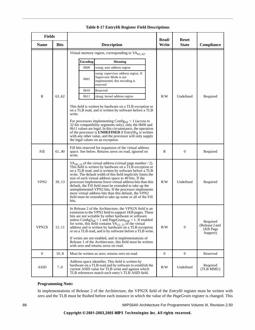
88 MIPS64® Architecture For Programmers Volume III, Revision 2.50
Copyright © 2001-2003,2005 MIPS Technologies Inc. All rights reserved.
Programming Note:
In implementations of Release 2 of the Architecture, the VPN2X field of the EntryHi register must be written withzero and the TLB must be flushed before each instance in which the value of the PageGrain register is changed. This
Table 8-17 EntryHi Register Field Descriptions
Fields
DescriptionRead/Write
ResetState ComplianceName Bits
R 63..62
Virtual memory region, corresponding to VA63..62.
This field is written by hardware on a TLB exception oron a TLB read, and is written by software before a TLBwrite.
For processors implementing ConfigAT = 1 (access to32-bit compatibility segments only), only the 0b00 and0b11 values are legal. In this circumstance, the operationof the processor is UNDEFINED if EntryHiR is writtenwith any other value, and the processor will only supplythe legal values on an exception.
R/W Undefined Required
Fill 61..40Fill bits reserved for expansion of the virtual addressspace. See below. Returns zeros on read, ignored onwrite.
R 0 Required
VPN2 39..13
VA39..13 of the virtual address (virtual page number / 2).This field is written by hardware on a TLB exception oron a TLB read, and is written by software before a TLBwrite. The default width of this field implicitly limits thesize of each virtual address space to 40 bits. If theprocessor implements fewer virtual address bits than thisdefault, the Fill field must be extended to take up theunimplemented VPN2 bits. If the processor implementsmore virtual address bits than this default, the VPN2field must be extended to take up some or all of the Fillbits.
R/W Undefined Required
VPN2X 12..11
In Release 2 of the Architecture, the VPN2X field is anextension to the VPN2 field to support 1KB pages. Thesebits are not writable by either hardware or softwareunless Config3SP = 1 and PageGrainESP = 1. If enabledfor write, this field contains VA12..11 of the virtualaddress and is written by hardware on a TLB exceptionor on a TLB read, and is by software before a TLB write.
If writes are not enabled, and in implementations ofRelease 1 of the Architecture, this field must be writtenwith zero and returns zeros on read.
R/W 0
Required(Release 2 and
1KB PageSupport)
0 10..8 Must be written as zero; returns zero on read. 0 0 Reserved
ASID 7..0
Address space identifier. This field is written byhardware on a TLB read and by software to establish thecurrent ASID value for TLB write and against whichTLB references match each entry’s TLB ASID field.
R/W Undefined Required(TLB MMU)
Encoding Meaning
0b00 xuseg: user address region
0b01
xsseg: supervisor address region. IfSupervisor Mode is notimplemented, this encoding isreserved
0b10 Reserved
0b11 xkseg: kernel address region
8.15 EntryHi Register (CP0 Register 10, Select 0)
MIPS64® Architecture For Programmers Volume III, Revision 2.50 89
Copyright © 2001-2003,2005 MIPS Technologies Inc. All rights reserved.
operation must be carried out while running in an unmapped address space. The operation of the processor is UNDE-FINED if this sequence is not done.
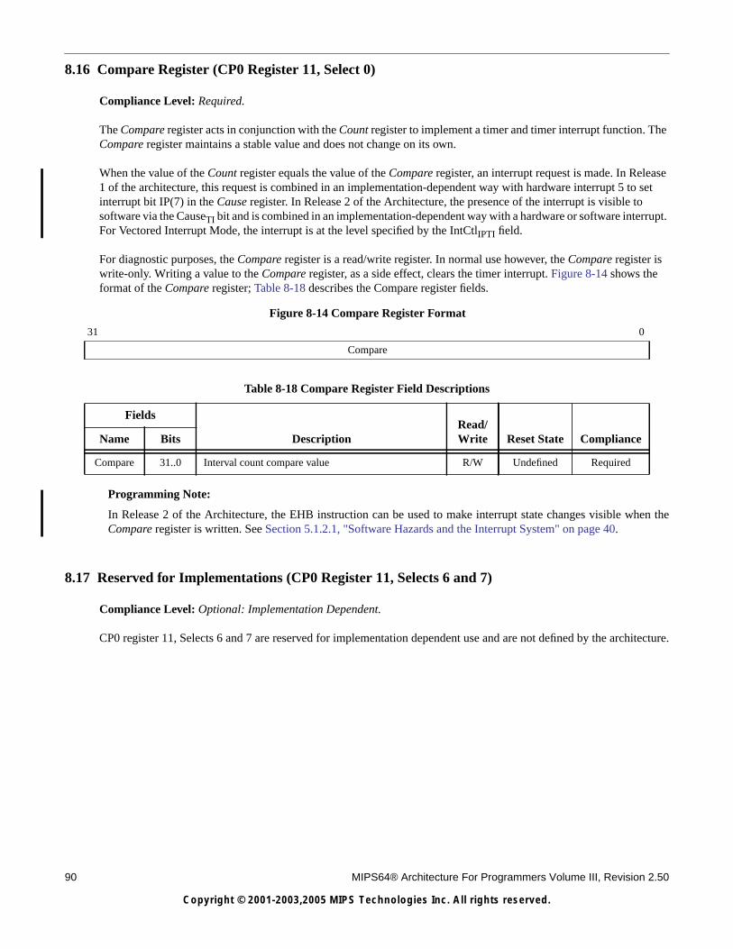
90 MIPS64® Architecture For Programmers Volume III, Revision 2.50
Copyright © 2001-2003,2005 MIPS Technologies Inc. All rights reserved.
8.16 Compare Register (CP0 Register 11, Select 0)
Compliance Level: Required.
The Compare register acts in conjunction with the Count register to implement a timer and timer interrupt function. TheCompare register maintains a stable value and does not change on its own.
When the value of the Count register equals the value of the Compare register, an interrupt request is made. In Release1 of the architecture, this request is combined in an implementation-dependent way with hardware interrupt 5 to setinterrupt bit IP(7) in the Cause register. In Release 2 of the Architecture, the presence of the interrupt is visible tosoftware via the CauseTI bit and is combined in an implementation-dependent way with a hardware or software interrupt.For Vectored Interrupt Mode, the interrupt is at the level specified by the IntCtlIPTI field.
For diagnostic purposes, the Compare register is a read/write register. In normal use however, the Compare register iswrite-only. Writing a value to the Compare register, as a side effect, clears the timer interrupt. Figure 8-14 shows theformat of the Compare register; Table 8-18 describes the Compare register fields.
Programming Note:
In Release 2 of the Architecture, the EHB instruction can be used to make interrupt state changes visible when theCompare register is written. See Section 5.1.2.1, "Software Hazards and the Interrupt System" on page 40.
8.17 Reserved for Implementations (CP0 Register 11, Selects 6 and 7)
Compliance Level: Optional: Implementation Dependent.
CP0 register 11, Selects 6 and 7 are reserved for implementation dependent use and are not defined by the architecture.
Figure 8-14 Compare Register Format
31 0
Compare
Table 8-18 Compare Register Field Descriptions
Fields
DescriptionRead/Write Reset State ComplianceName Bits
Compare 31..0 Interval count compare value R/W Undefined Required

8.18 Status Register (CP Register 12, Select 0)
MIPS64® Architecture For Programmers Volume III, Revision 2.50 91
Copyright © 2001-2003,2005 MIPS Technologies Inc. All rights reserved.
8.18 Status Register (CP Register 12, Select 0)
Compliance Level: Required.
The Status register is a read/write register that contains the operating mode, interrupt enabling, and the diagnostic statesof the processor. Fields of this register combine to create operating modes for the processor. Refer to Chapter 3, “MIPS64Operating Modes,” on page 9 for a discussion of operating modes, and Section Section 5.1, "Interrupts" on page 31 fora discussion of interrupt modes.
Figure 8-15 shows the format of the Status register; Table 8-19 describes the Status register fields.
Figure 8-15 Status Register Format
31 28 27 26 25 24 23 22 21 20 19 18 17 16 15 10 9 8 7 6 5 4 3 2 1 0
CU3..CU0 RP FR RE MX PX BEV TS SR NMI 0 Impl IM7..IM2 IM1..IM0 KX SX UX UM R0 ERL EXL IE
IPL KSU
Table 8-19 Status Register Field Descriptions
Fields
DescriptionRead/Writ
e Reset State ComplianceName Bits
CU(CU3..CU0)
31..28
Controls access to coprocessors 3, 2, 1, and 0,respectively:
Coprocessor 0 is always usable when the processor isrunning in Kernel Mode or Debug Mode, independent ofthe state of the CU0 bit.
In Release 2 of the Architecture, and for 64-bitimplementations of Release 1 of the Architecture,execution of all floating point instructions, including thoseencoded with the COP1X opcode, is controlled by theCU1 enable. CU3 is no longer used and is reserved forfuture use by the Architecture.
If there is no provision for connecting a coprocessor, thecorresponding CU bit must be ignored on write and readas zero.
R/W Undefined
Required forall
implementedcoprocessors
RP 27
Enables reduced power mode on some implementations.The specific operation of this bit is implementationdependent.
If this bit is not implemented, it must be ignored on writeand read as zero. If this bit is implemented, the reset statemust be zero so that the processor starts at fullperformance.
R/W 0 Optional
Encoding Meaning
0 Access not allowed
1 Access allowed
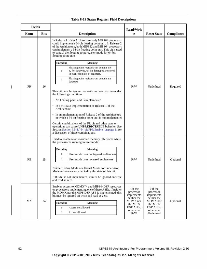
92 MIPS64® Architecture For Programmers Volume III, Revision 2.50
Copyright © 2001-2003,2005 MIPS Technologies Inc. All rights reserved.
FR 26
In Release 1 of the Architecture, only MIPS64 processorscould implement a 64-bit floating point unit. In Release 2of the Architecture, both MIPS32 and MIPS64 processorscan implement a 64-bit floating point unit. This bit is usedto control the floating point register mode for 64-bitfloating point units:
This bit must be ignored on write and read as zero underthe following conditions:
• No floating point unit is implemented
• In a MIPS32 implementation of Release 1 of theArchitecture
• In an implementation of Release 2 of the Architecturein which a 64-bit floating point unit is not implemented
Certain combinations of the FR bit and other state oroperations can cause UNPREDICTABLE behavior. SeeSection Section 3.5.4, "64-bit FPR Enable" on page 11 fora discussion of these combinations.
R/W Undefined Required
RE 25
Used to enable reverse-endian memory references whilethe processor is running in user mode:
Neither Debug Mode nor Kernel Mode nor SupervisorMode references are affected by the state of this bit.
If this bit is not implemented, it must be ignored on writeand read as zero.
R/W Undefined Optional
MX 24
Enables access to MDMX™ and MIPS® DSP resourceson processors implementing one of these ASEs. If neitherthe MDMX nor the MIPS DSP ASE is implemented, thisbit must be ignored on write and read as zero.
R if theprocessor
implementsneither the
MDMX northe MIPS
DSP ASEs;otherwise
R/W
0 if theprocessor
implementsneither the
MDMX northe MIPS
DSP ASEs;otherwiseUndefined
Optional
Table 8-19 Status Register Field Descriptions
Fields
DescriptionRead/Writ
e Reset State ComplianceName Bits
Encoding Meaning
0Floating point registers can contain any32-bit datatype. 64-bit datatypes are storedin even-odd pairs of registers.
1Floating point registers can contain anydatatype
Encoding Meaning
0 User mode uses configured endianness
1 User mode uses reversed endianness
Encoding Meaning
0 Access not allowed
1 Access allowed
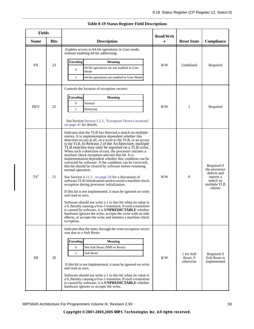
8.18 Status Register (CP Register 12, Select 0)
MIPS64® Architecture For Programmers Volume III, Revision 2.50 93
Copyright © 2001-2003,2005 MIPS Technologies Inc. All rights reserved.
PX 23
Enables access to 64-bit operations in User mode,without enabling 64-bit addressing:
R/W Undefined Required
BEV 22
Controls the location of exception vectors:
See Section Section 5.2.1, "Exception Vector Locations"on page 41 for details.
R/W 1 Required
TS1 21
Indicates that the TLB has detected a match on multipleentries. It is implementation dependent whether thisdetection occurs at all, on a write to the TLB, or an accessto the TLB. In Release 2 of the Architecture, multipleTLB matches may only be reported on a TLB write.When such a detection occurs, the processor initiates amachine check exception and sets this bit. It isimplementation dependent whether this condition can becorrected by software. If the condition can be corrected,this bit should be cleared by software before resumingnormal operation.
See Section 4.11.3 on page 24 for a discussion ofsoftware TLB initialization used to avoid a machine checkexception during processor initialization.
If this bit is not implemented, it must be ignored on writeand read as zero.
Software should not write a 1 to this bit when its value isa 0, thereby causing a 0-to-1 transition. If such a transitionis caused by software, it is UNPREDICTABLE whetherhardware ignores the write, accepts the write with no sideeffects, or accepts the write and initiates a machine checkexception.
R/W 0
Required ifthe processordetects andreports amatch on
multiple TLBentries
SR 20
Indicates that the entry through the reset exception vectorwas due to a Soft Reset:
If this bit is not implemented, it must be ignored on writeand read as zero.
Software should not write a 1 to this bit when its value isa 0, thereby causing a 0-to-1 transition. If such a transitionis caused by software, it is UNPREDICTABLE whetherhardware ignores or accepts the write.
R/W1 for SoftReset; 0
otherwise
Required ifSoft Reset isimplemented
Table 8-19 Status Register Field Descriptions
Fields
DescriptionRead/Writ
e Reset State ComplianceName Bits
Encoding Meaning
064-bit operations are not enabled in UserMode
1 64-bit operations are enabled in User Mode
Encoding Meaning
0 Normal
1 Bootstrap
Encoding Meaning
0 Not Soft Reset (NMI or Reset)
1 Soft Reset
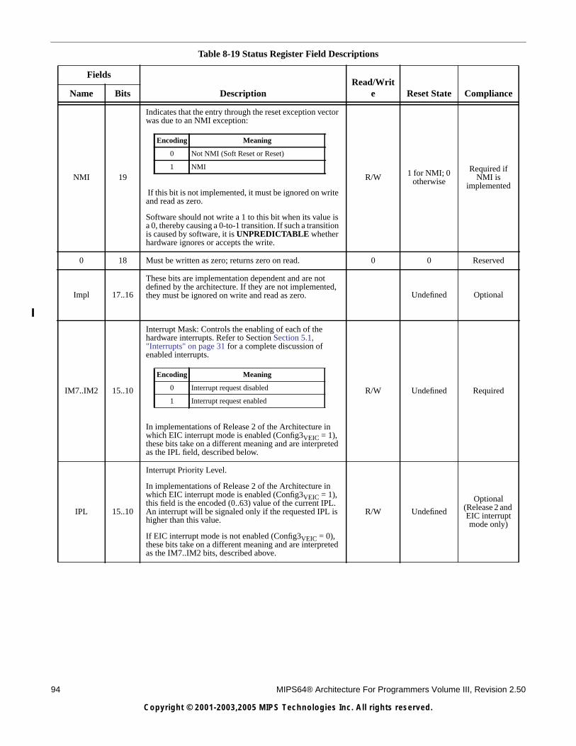
94 MIPS64® Architecture For Programmers Volume III, Revision 2.50
Copyright © 2001-2003,2005 MIPS Technologies Inc. All rights reserved.
NMI 19
Indicates that the entry through the reset exception vectorwas due to an NMI exception:
If this bit is not implemented, it must be ignored on writeand read as zero.
Software should not write a 1 to this bit when its value isa 0, thereby causing a 0-to-1 transition. If such a transitionis caused by software, it is UNPREDICTABLE whetherhardware ignores or accepts the write.
R/W 1 for NMI; 0otherwise
Required ifNMI is
implemented
0 18 Must be written as zero; returns zero on read. 0 0 Reserved
Impl 17..16
These bits are implementation dependent and are notdefined by the architecture. If they are not implemented,they must be ignored on write and read as zero. Undefined Optional
IM7..IM2 15..10
Interrupt Mask: Controls the enabling of each of thehardware interrupts. Refer to Section Section 5.1,"Interrupts" on page 31 for a complete discussion ofenabled interrupts.
In implementations of Release 2 of the Architecture inwhich EIC interrupt mode is enabled (Config3VEIC = 1),these bits take on a different meaning and are interpretedas the IPL field, described below.
R/W Undefined Required
IPL 15..10
Interrupt Priority Level.
In implementations of Release 2 of the Architecture inwhich EIC interrupt mode is enabled (Config3VEIC = 1),this field is the encoded (0..63) value of the current IPL.An interrupt will be signaled only if the requested IPL ishigher than this value.
If EIC interrupt mode is not enabled (Config3VEIC = 0),these bits take on a different meaning and are interpretedas the IM7..IM2 bits, described above.
R/W Undefined
Optional(Release 2 andEIC interruptmode only)
Table 8-19 Status Register Field Descriptions
Fields
DescriptionRead/Writ
e Reset State ComplianceName Bits
Encoding Meaning
0 Not NMI (Soft Reset or Reset)
1 NMI
Encoding Meaning
0 Interrupt request disabled
1 Interrupt request enabled
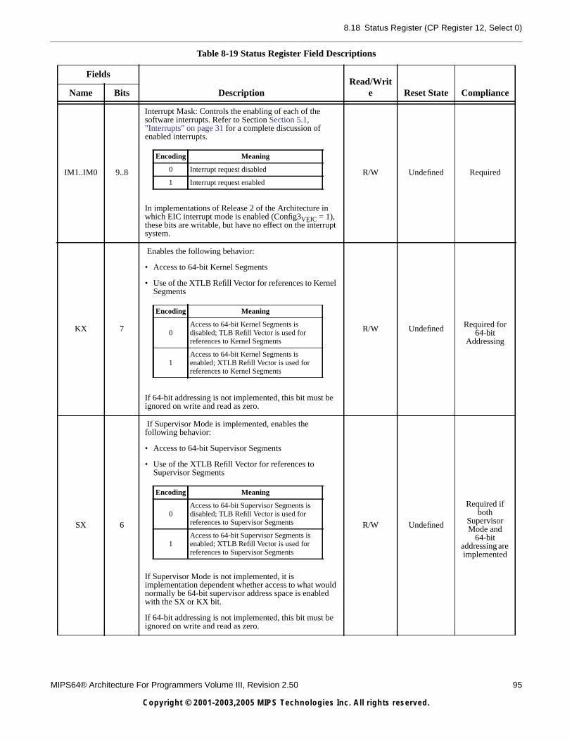
8.18 Status Register (CP Register 12, Select 0)
MIPS64® Architecture For Programmers Volume III, Revision 2.50 95
Copyright © 2001-2003,2005 MIPS Technologies Inc. All rights reserved.
IM1..IM0 9..8
Interrupt Mask: Controls the enabling of each of thesoftware interrupts. Refer to Section Section 5.1,"Interrupts" on page 31 for a complete discussion ofenabled interrupts.
In implementations of Release 2 of the Architecture inwhich EIC interrupt mode is enabled (Config3VEIC = 1),these bits are writable, but have no effect on the interruptsystem.
R/W Undefined Required
KX 7
Enables the following behavior:
• Access to 64-bit Kernel Segments
• Use of the XTLB Refill Vector for references to KernelSegments
If 64-bit addressing is not implemented, this bit must beignored on write and read as zero.
R/W Undefined Required for64-bit
Addressing
SX 6
If Supervisor Mode is implemented, enables thefollowing behavior:
• Access to 64-bit Supervisor Segments
• Use of the XTLB Refill Vector for references toSupervisor Segments
If Supervisor Mode is not implemented, it isimplementation dependent whether access to what wouldnormally be 64-bit supervisor address space is enabledwith the SX or KX bit.
If 64-bit addressing is not implemented, this bit must beignored on write and read as zero.
R/W Undefined
Required ifboth
SupervisorMode and
64-bitaddressing areimplemented
Table 8-19 Status Register Field Descriptions
Fields
DescriptionRead/Writ
e Reset State ComplianceName Bits
Encoding Meaning
0 Interrupt request disabled
1 Interrupt request enabled
Encoding Meaning
0Access to 64-bit Kernel Segments isdisabled; TLB Refill Vector is used forreferences to Kernel Segments
1Access to 64-bit Kernel Segments isenabled; XTLB Refill Vector is used forreferences to Kernel Segments
Encoding Meaning
0Access to 64-bit Supervisor Segments isdisabled; TLB Refill Vector is used forreferences to Supervisor Segments
1Access to 64-bit Supervisor Segments isenabled; XTLB Refill Vector is used forreferences to Supervisor Segments
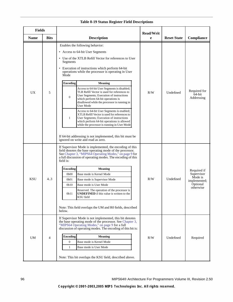
96 MIPS64® Architecture For Programmers Volume III, Revision 2.50
Copyright © 2001-2003,2005 MIPS Technologies Inc. All rights reserved.
UX 5
Enables the following behavior:
• Access to 64-bit User Segments
• Use of the XTLB Refill Vector for references to UserSegments
• Execution of instructions which perform 64-bitoperations while the processor is operating in UserMode
If 64-bit addressing is not implemented, this bit must beignored on write and read as zero.
R/W Undefined Required for64-bit
Addressing
KSU 4..3
If Supervisor Mode is implemented, the encoding of thisfield denotes the base operating mode of the processor.See Chapter 3, “MIPS64 Operating Modes,” on page 9 fora full discussion of operating modes. The encoding of thisfield is:
Note: This field overlaps the UM and R0 fields, describedbelow.
R/W Undefined
Required ifSupervisor
Mode isimplemented;
Optionalotherwise
UM 4
If Supervisor Mode is not implemented, this bit denotesthe base operating mode of the processor. See Chapter 3,“MIPS64 Operating Modes,” on page 9 for a fulldiscussion of operating modes. The encoding of this bit is:
Note: This bit overlaps the KSU field, described above.
R/W Undefined Required
Table 8-19 Status Register Field Descriptions
Fields
DescriptionRead/Writ
e Reset State ComplianceName Bits
Encoding Meaning
0
Access to 64-bit User Segments is disabled;TLB Refill Vector is used for references toUser Segments; Execution of instructionswhich perform 64-bit operations isdisallowed while the processor is running inUser Mode
1
Access to 64-bit User Segments is enabled;XTLB Refill Vector is used for references toUser Segments; Execution of instructionswhich perform 64-bit operations is allowedwhile the processor is running in User Mode
Encoding Meaning
0b00 Base mode is Kernel Mode
0b01 Base mode is Supervisor Mode
0b10 Base mode is User Mode
0b11Reserved. The operation of the processor isUNDEFINED if this value is written to theKSU field
Encoding Meaning
0 Base mode is Kernel Mode
1 Base mode is User Mode
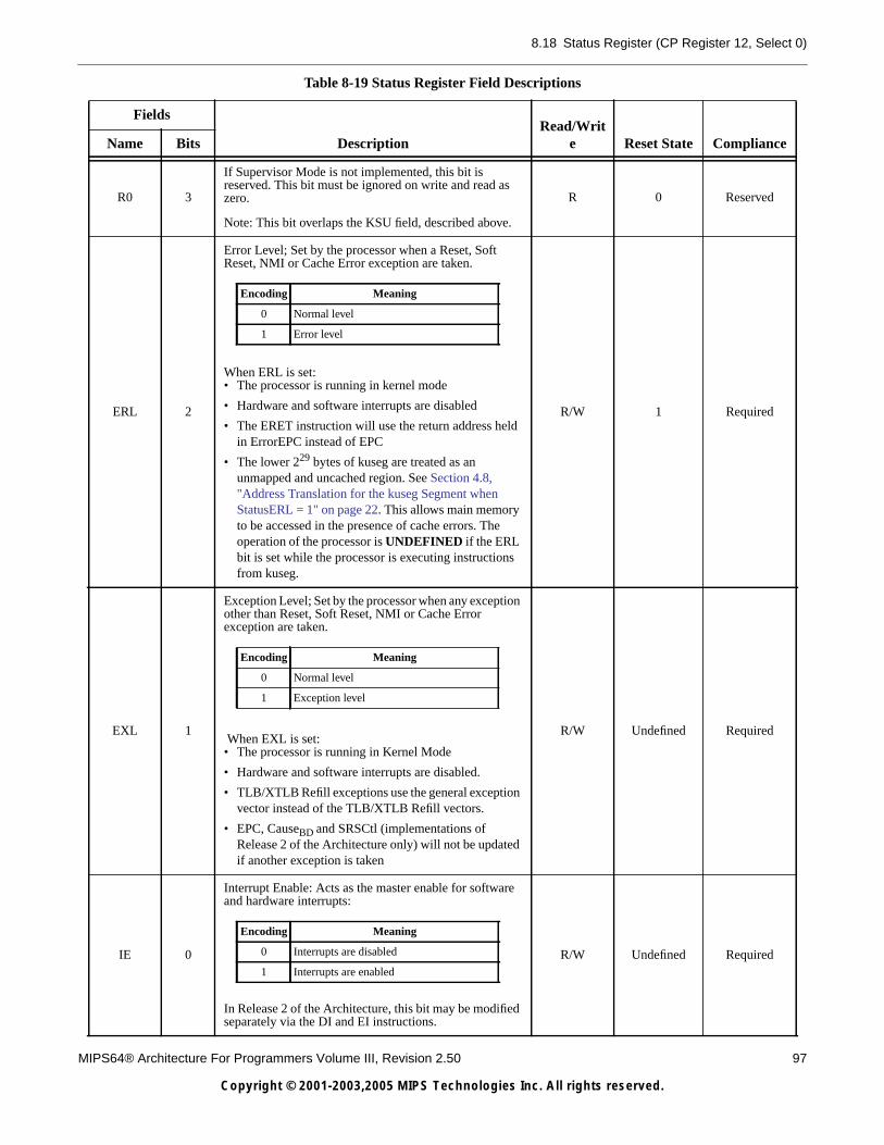
8.18 Status Register (CP Register 12, Select 0)
MIPS64® Architecture For Programmers Volume III, Revision 2.50 97
Copyright © 2001-2003,2005 MIPS Technologies Inc. All rights reserved.
R0 3
If Supervisor Mode is not implemented, this bit isreserved. This bit must be ignored on write and read aszero.
Note: This bit overlaps the KSU field, described above.
R 0 Reserved
ERL 2
Error Level; Set by the processor when a Reset, SoftReset, NMI or Cache Error exception are taken.
When ERL is set:• The processor is running in kernel mode
• Hardware and software interrupts are disabled
• The ERET instruction will use the return address heldin ErrorEPC instead of EPC
• The lower 229 bytes of kuseg are treated as anunmapped and uncached region. See Section 4.8,"Address Translation for the kuseg Segment whenStatusERL = 1" on page 22. This allows main memoryto be accessed in the presence of cache errors. Theoperation of the processor is UNDEFINED if the ERLbit is set while the processor is executing instructionsfrom kuseg.
R/W 1 Required
EXL 1
Exception Level; Set by the processor when any exceptionother than Reset, Soft Reset, NMI or Cache Errorexception are taken.
When EXL is set:• The processor is running in Kernel Mode
• Hardware and software interrupts are disabled.
• TLB/XTLB Refill exceptions use the general exceptionvector instead of the TLB/XTLB Refill vectors.
• EPC, CauseBD and SRSCtl (implementations ofRelease 2 of the Architecture only) will not be updatedif another exception is taken
R/W Undefined Required
IE 0
Interrupt Enable: Acts as the master enable for softwareand hardware interrupts:
In Release 2 of the Architecture, this bit may be modifiedseparately via the DI and EI instructions.
R/W Undefined Required
Table 8-19 Status Register Field Descriptions
Fields
DescriptionRead/Writ
e Reset State ComplianceName Bits
Encoding Meaning
0 Normal level
1 Error level
Encoding Meaning
0 Normal level
1 Exception level
Encoding Meaning
0 Interrupts are disabled
1 Interrupts are enabled
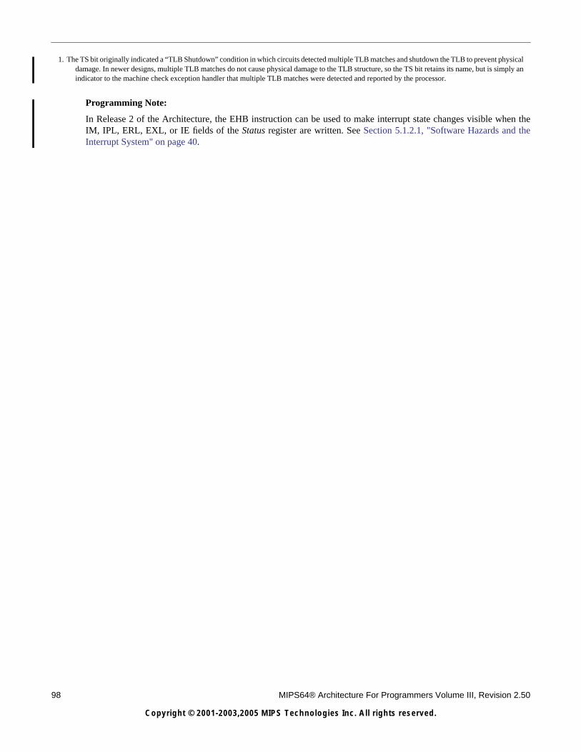
98 MIPS64® Architecture For Programmers Volume III, Revision 2.50
Copyright © 2001-2003,2005 MIPS Technologies Inc. All rights reserved.
Programming Note:
In Release 2 of the Architecture, the EHB instruction can be used to make interrupt state changes visible when theIM, IPL, ERL, EXL, or IE fields of the Status register are written. See Section 5.1.2.1, "Software Hazards and theInterrupt System" on page 40.
1. The TS bit originally indicated a “TLB Shutdown” condition in which circuits detected multiple TLB matches and shutdown the TLB to prevent physicaldamage. In newer designs, multiple TLB matches do not cause physical damage to the TLB structure, so the TS bit retains its name, but is simply anindicator to the machine check exception handler that multiple TLB matches were detected and reported by the processor.
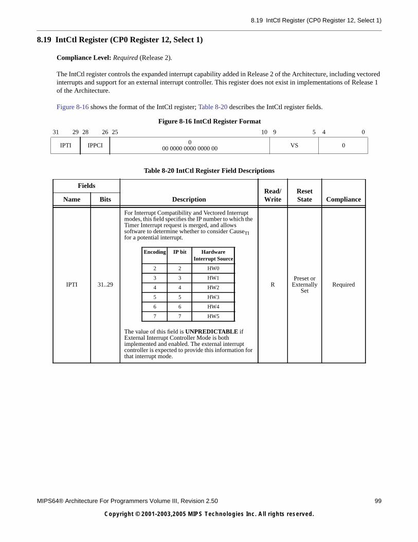
8.19 IntCtl Register (CP0 Register 12, Select 1)
MIPS64® Architecture For Programmers Volume III, Revision 2.50 99
Copyright © 2001-2003,2005 MIPS Technologies Inc. All rights reserved.
8.19 IntCtl Register (CP0 Register 12, Select 1)
Compliance Level: Required (Release 2).
The IntCtl register controls the expanded interrupt capability added in Release 2 of the Architecture, including vectoredinterrupts and support for an external interrupt controller. This register does not exist in implementations of Release 1of the Architecture.
Figure 8-16 shows the format of the IntCtl register; Table 8-20 describes the IntCtl register fields.
Figure 8-16 IntCtl Register Format
31 29 28 26 25 10 9 5 4 0
IPTI IPPCI 000 0000 0000 0000 00 VS 0
Table 8-20 IntCtl Register Field Descriptions
Fields
DescriptionRead/Write
ResetState ComplianceName Bits
IPTI 31..29
For Interrupt Compatibility and Vectored Interruptmodes, this field specifies the IP number to which theTimer Interrupt request is merged, and allowssoftware to determine whether to consider CauseTIfor a potential interrupt.
The value of this field is UNPREDICTABLE ifExternal Interrupt Controller Mode is bothimplemented and enabled. The external interruptcontroller is expected to provide this information forthat interrupt mode.
RPreset or
ExternallySet
Required
Encoding IP bit HardwareInterrupt Source
2 2 HW0
3 3 HW1
4 4 HW2
5 5 HW3
6 6 HW4
7 7 HW5
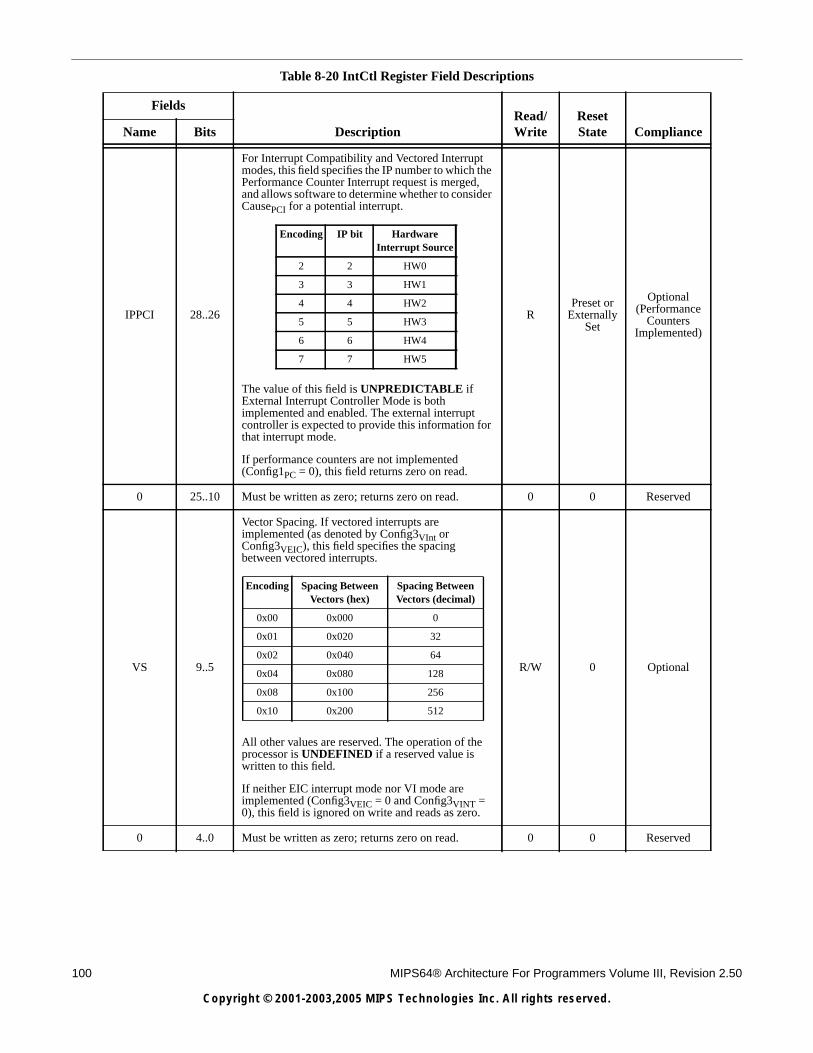
100 MIPS64® Architecture For Programmers Volume III, Revision 2.50
Copyright © 2001-2003,2005 MIPS Technologies Inc. All rights reserved.
IPPCI 28..26
For Interrupt Compatibility and Vectored Interruptmodes, this field specifies the IP number to which thePerformance Counter Interrupt request is merged,and allows software to determine whether to considerCausePCI for a potential interrupt.
The value of this field is UNPREDICTABLE ifExternal Interrupt Controller Mode is bothimplemented and enabled. The external interruptcontroller is expected to provide this information forthat interrupt mode.
If performance counters are not implemented(Config1PC = 0), this field returns zero on read.
RPreset or
ExternallySet
Optional(Performance
CountersImplemented)
0 25..10 Must be written as zero; returns zero on read. 0 0 Reserved
VS 9..5
Vector Spacing. If vectored interrupts areimplemented (as denoted by Config3VInt orConfig3VEIC), this field specifies the spacingbetween vectored interrupts.
All other values are reserved. The operation of theprocessor is UNDEFINED if a reserved value iswritten to this field.
If neither EIC interrupt mode nor VI mode areimplemented (Config3VEIC = 0 and Config3VINT =0), this field is ignored on write and reads as zero.
R/W 0 Optional
0 4..0 Must be written as zero; returns zero on read. 0 0 Reserved
Table 8-20 IntCtl Register Field Descriptions
Fields
DescriptionRead/Write
ResetState ComplianceName Bits
Encoding IP bit HardwareInterrupt Source
2 2 HW0
3 3 HW1
4 4 HW2
5 5 HW3
6 6 HW4
7 7 HW5
Encoding Spacing BetweenVectors (hex)
Spacing BetweenVectors (decimal)
0x00 0x000 0
0x01 0x020 32
0x02 0x040 64
0x04 0x080 128
0x08 0x100 256
0x10 0x200 512
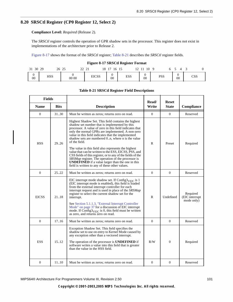
8.20 SRSCtl Register (CP0 Register 12, Select 2)
MIPS64® Architecture For Programmers Volume III, Revision 2.50 101
Copyright © 2001-2003,2005 MIPS Technologies Inc. All rights reserved.
8.20 SRSCtl Register (CP0 Register 12, Select 2)
Compliance Level: Required (Release 2).
The SRSCtl register controls the operation of GPR shadow sets in the processor. This register does not exist inimplementations of the architecture prior to Release 2.
Figure 8-17 shows the format of the SRSCtl register; Table 8-21 describes the SRSCtl register fields.
Figure 8-17 SRSCtl Register Format
31 30 29 26 25 22 21 18 17 16 15 12 11 10 9 6 5 4 3 0
000 HSS 0
00 00 EICSS 000 ESS 0
00 PSS 000 CSS
Table 8-21 SRSCtl Register Field Descriptions
Fields
DescriptionRead/Write
ResetState ComplianceName Bits
0 31..30 Must be written as zeros; returns zero on read. 0 0 Reserved
HSS 29..26
Highest Shadow Set. This field contains the highestshadow set number that is implemented by thisprocessor. A value of zero in this field indicates thatonly the normal GPRs are implemented. A non-zerovalue in this field indicates that the implementedshadow sets are numbered 0..n, where n is the valueof the field.
The value in this field also represents the highestvalue that can be written to the ESS, EICSS, PSS, andCSS fields of this register, or to any of the fields of theSRSMap register. The operation of the processor isUNDEFINED if a value larger than the one in thisfield is written to any of these other values.
R Preset Required
0 25..22 Must be written as zeros; returns zero on read. 0 0 Reserved
EICSS 21..18
EIC interrupt mode shadow set. If Config3VEIC is 1(EIC interrupt mode is enabled), this field is loadedfrom the external interrupt controller for eachinterrupt request and is used in place of the SRSMapregister to select the current shadow set for theinterrupt.
See Section 5.1.1.3, "External Interrupt ControllerMode" on page 37 for a discussion of EIC interruptmode. If Config3VEIC is 0, this field must be writtenas zero, and returns zero on read.
R UndefinedRequired
(EIC interruptmode only)
0 17..16 Must be written as zeros; returns zero on read. 0 0 Reserved
ESS 15..12
Exception Shadow Set. This field specifies theshadow set to use on entry to Kernel Mode caused byany exception other than a vectored interrupt.
The operation of the processor is UNDEFINED ifsoftware writes a value into this field that is greaterthan the value in the HSS field.
R/W 0 Required
0 11..10 Must be written as zeros; returns zero on read. 0 0 Reserved
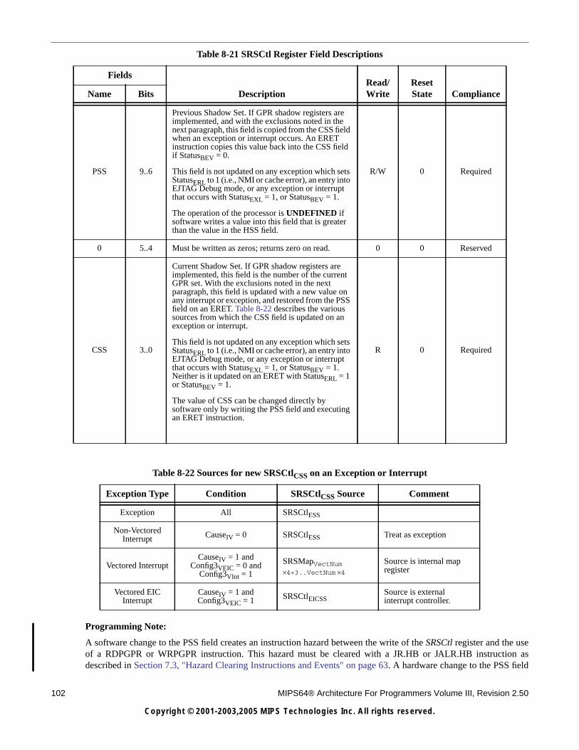
102 MIPS64® Architecture For Programmers Volume III, Revision 2.50
Copyright © 2001-2003,2005 MIPS Technologies Inc. All rights reserved.
Programming Note:
A software change to the PSS field creates an instruction hazard between the write of the SRSCtl register and the useof a RDPGPR or WRPGPR instruction. This hazard must be cleared with a JR.HB or JALR.HB instruction asdescribed in Section 7.3, "Hazard Clearing Instructions and Events" on page 63. A hardware change to the PSS field
PSS 9..6
Previous Shadow Set. If GPR shadow registers areimplemented, and with the exclusions noted in thenext paragraph, this field is copied from the CSS fieldwhen an exception or interrupt occurs. An ERETinstruction copies this value back into the CSS fieldif StatusBEV = 0.
This field is not updated on any exception which setsStatusERL to 1 (i.e., NMI or cache error), an entry intoEJTAG Debug mode, or any exception or interruptthat occurs with StatusEXL = 1, or StatusBEV = 1.
The operation of the processor is UNDEFINED ifsoftware writes a value into this field that is greaterthan the value in the HSS field.
R/W 0 Required
0 5..4 Must be written as zeros; returns zero on read. 0 0 Reserved
CSS 3..0
Current Shadow Set. If GPR shadow registers areimplemented, this field is the number of the currentGPR set. With the exclusions noted in the nextparagraph, this field is updated with a new value onany interrupt or exception, and restored from the PSSfield on an ERET. Table 8-22 describes the varioussources from which the CSS field is updated on anexception or interrupt.
This field is not updated on any exception which setsStatusERL to 1 (i.e., NMI or cache error), an entry intoEJTAG Debug mode, or any exception or interruptthat occurs with StatusEXL = 1, or StatusBEV = 1.Neither is it updated on an ERET with StatusERL = 1or StatusBEV = 1.
The value of CSS can be changed directly bysoftware only by writing the PSS field and executingan ERET instruction.
R 0 Required
Table 8-22 Sources for new SRSCtlCSS on an Exception or Interrupt
Exception Type Condition SRSCtlCSS Source Comment
Exception All SRSCtlESS
Non-VectoredInterrupt CauseIV = 0 SRSCtlESS Treat as exception
Vectored InterruptCauseIV = 1 and
Config3VEIC = 0 andConfig3VInt = 1
SRSMapVectNum×4+3..VectNum ×4
Source is internal mapregister
Vectored EICInterrupt
CauseIV = 1 andConfig3VEIC = 1 SRSCtlEICSS
Source is externalinterrupt controller.
Table 8-21 SRSCtl Register Field Descriptions
Fields
DescriptionRead/Write
ResetState ComplianceName Bits
8.20 SRSCtl Register (CP0 Register 12, Select 2)
MIPS64® Architecture For Programmers Volume III, Revision 2.50 103
Copyright © 2001-2003,2005 MIPS Technologies Inc. All rights reserved.
as the result of interrupt or exception entry is automatically cleared for the execution of the first instruction in theinterrupt or exception handler.
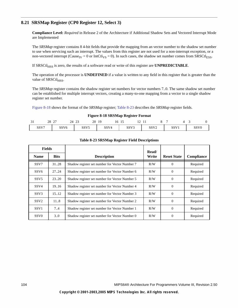
104 MIPS64® Architecture For Programmers Volume III, Revision 2.50
Copyright © 2001-2003,2005 MIPS Technologies Inc. All rights reserved.
8.21 SRSMap Register (CP0 Register 12, Select 3)
Compliance Level: Required in Release 2 of the Architecture if Additional Shadow Sets and Vectored Interrupt Modeare Implemented
The SRSMap register contains 8 4-bit fields that provide the mapping from an vector number to the shadow set numberto use when servicing such an interrupt. The values from this register are not used for a non-interrupt exception, or anon-vectored interrupt (CauseIV = 0 or IntCtlVS = 0). In such cases, the shadow set number comes from SRSCtlESS.
If SRSCtlHSS is zero, the results of a software read or write of this register are UNPREDICTABLE.
The operation of the processor is UNDEFINED if a value is written to any field in this register that is greater than thevalue of SRSCtlHSS.
The SRSMap register contains the shadow register set numbers for vector numbers 7..0. The same shadow set numbercan be established for multiple interrupt vectors, creating a many-to-one mapping from a vector to a single shadowregister set number.
Figure 8-18 shows the format of the SRSMap register; Table 8-23 describes the SRSMap register fields.
Figure 8-18 SRSMap Register Format
31 28 27 24 23 20 19 16 15 12 11 8 7 4 3 0
SSV7 SSV6 SSV5 SSV4 SSV3 SSV2 SSV1 SSV0
Table 8-23 SRSMap Register Field Descriptions
Fields
DescriptionRead/Write Reset State ComplianceName Bits
SSV7 31..28 Shadow register set number for Vector Number 7 R/W 0 Required
SSV6 27..24 Shadow register set number for Vector Number 6 R/W 0 Required
SSV5 23..20 Shadow register set number for Vector Number 5 R/W 0 Required
SSV4 19..16 Shadow register set number for Vector Number 4 R/W 0 Required
SSV3 15..12 Shadow register set number for Vector Number 3 R/W 0 Required
SSV2 11..8 Shadow register set number for Vector Number 2 R/W 0 Required
SSV1 7..4 Shadow register set number for Vector Number 1 R/W 0 Required
SSV0 3..0 Shadow register set number for Vector Number 0 R/W 0 Required
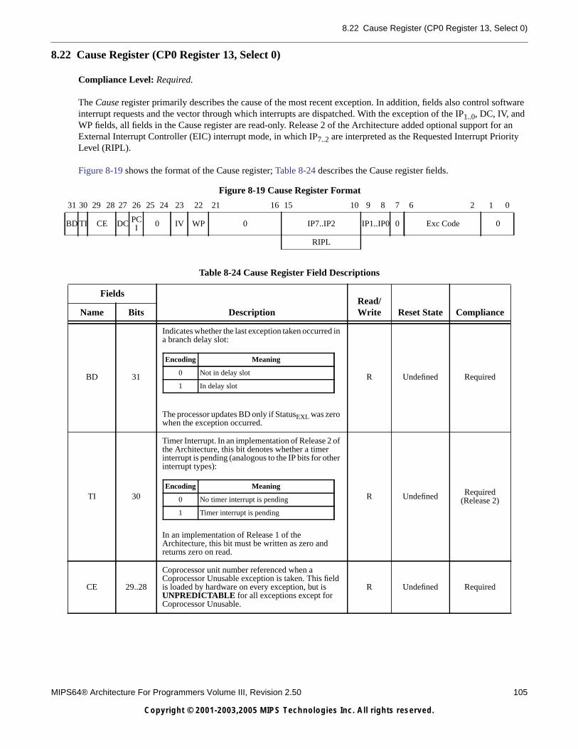
8.22 Cause Register (CP0 Register 13, Select 0)
MIPS64® Architecture For Programmers Volume III, Revision 2.50 105
Copyright © 2001-2003,2005 MIPS Technologies Inc. All rights reserved.
8.22 Cause Register (CP0 Register 13, Select 0)
Compliance Level: Required.
The Cause register primarily describes the cause of the most recent exception. In addition, fields also control softwareinterrupt requests and the vector through which interrupts are dispatched. With the exception of the IP1..0, DC, IV, andWP fields, all fields in the Cause register are read-only. Release 2 of the Architecture added optional support for anExternal Interrupt Controller (EIC) interrupt mode, in which IP7..2 are interpreted as the Requested Interrupt PriorityLevel (RIPL).
Figure 8-19 shows the format of the Cause register; Table 8-24 describes the Cause register fields.
Figure 8-19 Cause Register Format
31 30 29 28 27 26 25 24 23 22 21 16 15 10 9 8 7 6 2 1 0
BD TI CE DC PCI 0 IV WP 0 IP7..IP2 IP1..IP0 0 Exc Code 0
RIPL
Table 8-24 Cause Register Field Descriptions
Fields
DescriptionRead/Write Reset State ComplianceName Bits
BD 31
Indicates whether the last exception taken occurred ina branch delay slot:
The processor updates BD only if StatusEXL was zerowhen the exception occurred.
R Undefined Required
TI 30
Timer Interrupt. In an implementation of Release 2 ofthe Architecture, this bit denotes whether a timerinterrupt is pending (analogous to the IP bits for otherinterrupt types):
In an implementation of Release 1 of theArchitecture, this bit must be written as zero andreturns zero on read.
R Undefined Required(Release 2)
CE 29..28
Coprocessor unit number referenced when aCoprocessor Unusable exception is taken. This fieldis loaded by hardware on every exception, but isUNPREDICTABLE for all exceptions except forCoprocessor Unusable.
R Undefined Required
Encoding Meaning
0 Not in delay slot
1 In delay slot
Encoding Meaning
0 No timer interrupt is pending
1 Timer interrupt is pending
106 MIPS64® Architecture For Programmers Volume III, Revision 2.50
Copyright © 2001-2003,2005 MIPS Technologies Inc. All rights reserved.
DC 27
Disable Count register. In some power-sensitiveapplications, the Count register is not used but maystill be the source of some noticeable powerdissipation. This bit allows the Count register to bestopped in such situations.
In an implementation of Release 1 of theArchitecture, this bit must be written as zero, andreturns zero on read.
R/W 0 Required(Release 2)
PCI 26
Performance Counter Interrupt. In animplementation of Release 2 of the Architecture, thisbit denotes whether a performance counter interruptis pending (analogous to the IP bits for other interrupttypes):
In an implementation of Release 1 of theArchitecture, or if performance counters are notimplemented (Config1PC = 0), this bit must bewritten as zero and returns zero on read.
R Undefined
Required(Release 2 andperformance
countersimplemented)
IV 23
Indicates whether an interrupt exception uses thegeneral exception vector or a special interrupt vector:
In implementations of Release 2 of the architecture,if the CauseIV is 1 and StatusBEV is 0, the specialinterrupt vector represents the base of the vectoredinterrupt table.
R/W Undefined Required
Table 8-24 Cause Register Field Descriptions
Fields
DescriptionRead/Write Reset State ComplianceName Bits
Encoding Meaning
0 Enable counting of Count register
1 Disable counting of Count register
Encoding Meaning
0No performance counter interrupt ispending
1 Performance counter interrupt is pending
Encoding Meaning
0 Use the general exception vector (0x180)
1 Use the special interrupt vector (0x200)
8.22 Cause Register (CP0 Register 13, Select 0)
MIPS64® Architecture For Programmers Volume III, Revision 2.50 107
Copyright © 2001-2003,2005 MIPS Technologies Inc. All rights reserved.
WP 22
Indicates that a watch exception was deferredbecause StatusEXL or StatusERL were a one at thetime the watch exception was detected. This bit bothindicates that the watch exception was deferred, andcauses the exception to be initiated once StatusEXLand StatusERL are both zero. As such, software mustclear this bit as part of the watch exception handler toprevent a watch exception loop.
Software should not write a 1 to this bit when itsvalue is a 0, thereby causing a 0-to-1 transition. Ifsuch a transition is caused by software, it isUNPREDICTABLE whether hardware ignores thewrite, accepts the write with no side effects, oraccepts the write and initiates a watch exception onceStatusEXL and StatusERL are both zero.
If watch registers are not implemented, this bit mustbe ignored on write and read as zero.
R/W Undefined
Required ifwatch
registers areimplemented
IP7..IP2 15..10
Indicates an interrupt is pending:
In implementations of Release 1 of the Architecture,timer and performance counter interrupts arecombined in an implementation-dependent way withhardware interrupt 5.
In implementations of Release 2 of the Architecturein which EIC interrupt mode is not enabled(Config3VEIC = 0), timer and performance counterinterrupts are combined in animplementation-dependent way with any hardwareinterrupt. If EIC interrupt mode is enabled(Config3VEIC = 1), these bits take on a differentmeaning and are interpreted as the RIPL field,described below.
R Undefined Required
RIPL 15..10
Requested Interrupt Priority Level.
In implementations of Release 2 of the Architecturein which EIC interrupt mode is enabled (Config3VEIC= 1), this field is the encoded (0..63) value of therequested interrupt. A value of zero indicates that nointerrupt is requested.
If EIC interrupt mode is not enabled (Config3VEIC =0), these bits take on a different meaning and areinterpreted as the IP7..IP2 bits, described above.
R Undefined
Optional(Release 2 andEIC interruptmode only)
Table 8-24 Cause Register Field Descriptions
Fields
DescriptionRead/Write Reset State ComplianceName Bits
Bit Name Meaning
15 IP7 Hardware interrupt 5
14 IP6 Hardware interrupt 4
13 IP5 Hardware interrupt 3
12 IP4 Hardware interrupt 2
11 IP3 Hardware interrupt 1
10 IP2 Hardware interrupt 0
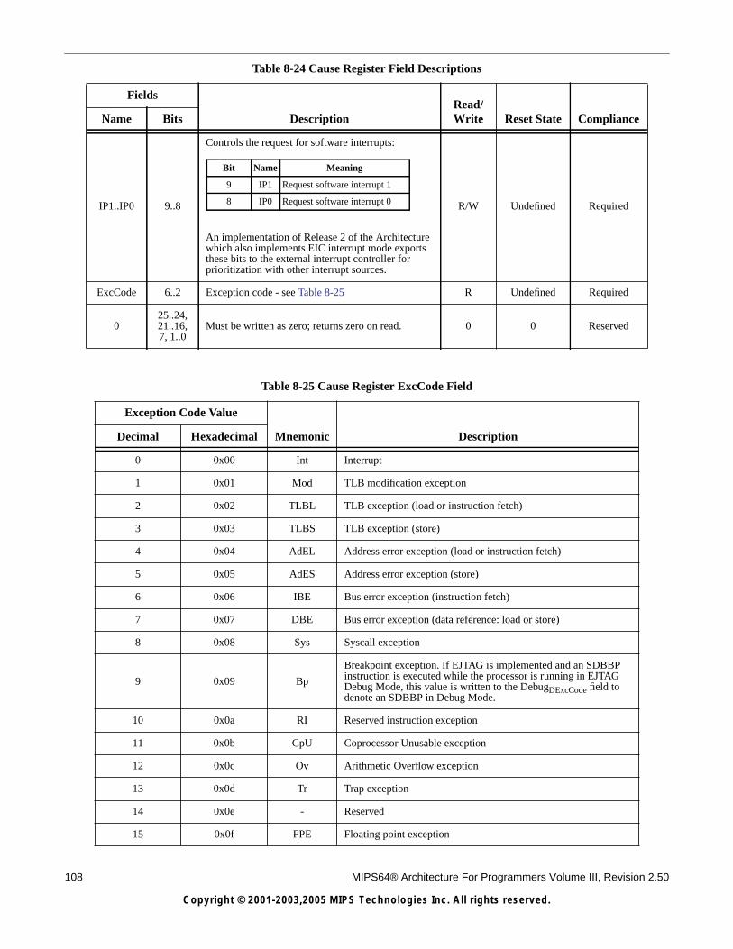
108 MIPS64® Architecture For Programmers Volume III, Revision 2.50
Copyright © 2001-2003,2005 MIPS Technologies Inc. All rights reserved.
IP1..IP0 9..8
Controls the request for software interrupts:
An implementation of Release 2 of the Architecturewhich also implements EIC interrupt mode exportsthese bits to the external interrupt controller forprioritization with other interrupt sources.
R/W Undefined Required
ExcCode 6..2 Exception code - see Table 8-25 R Undefined Required
025..24,21..16,7, 1..0
Must be written as zero; returns zero on read. 0 0 Reserved
Table 8-25 Cause Register ExcCode Field
Exception Code Value
Mnemonic DescriptionDecimal Hexadecimal
0 0x00 Int Interrupt
1 0x01 Mod TLB modification exception
2 0x02 TLBL TLB exception (load or instruction fetch)
3 0x03 TLBS TLB exception (store)
4 0x04 AdEL Address error exception (load or instruction fetch)
5 0x05 AdES Address error exception (store)
6 0x06 IBE Bus error exception (instruction fetch)
7 0x07 DBE Bus error exception (data reference: load or store)
8 0x08 Sys Syscall exception
9 0x09 Bp
Breakpoint exception. If EJTAG is implemented and an SDBBPinstruction is executed while the processor is running in EJTAGDebug Mode, this value is written to the DebugDExcCode field todenote an SDBBP in Debug Mode.
10 0x0a RI Reserved instruction exception
11 0x0b CpU Coprocessor Unusable exception
12 0x0c Ov Arithmetic Overflow exception
13 0x0d Tr Trap exception
14 0x0e - Reserved
15 0x0f FPE Floating point exception
Table 8-24 Cause Register Field Descriptions
Fields
DescriptionRead/Write Reset State ComplianceName Bits
Bit Name Meaning
9 IP1 Request software interrupt 1
8 IP0 Request software interrupt 0
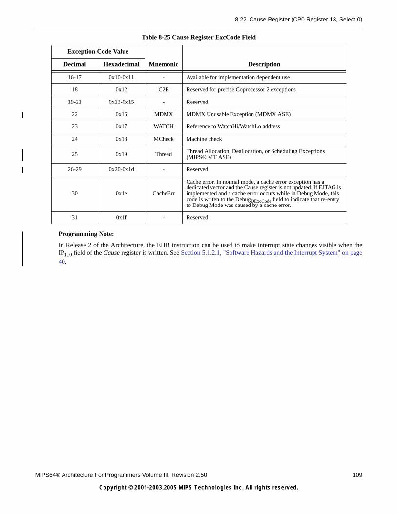
8.22 Cause Register (CP0 Register 13, Select 0)
MIPS64® Architecture For Programmers Volume III, Revision 2.50 109
Copyright © 2001-2003,2005 MIPS Technologies Inc. All rights reserved.
Programming Note:
In Release 2 of the Architecture, the EHB instruction can be used to make interrupt state changes visible when theIP1..0 field of the Cause register is written. See Section 5.1.2.1, "Software Hazards and the Interrupt System" on page40.
16-17 0x10-0x11 - Available for implementation dependent use
18 0x12 C2E Reserved for precise Coprocessor 2 exceptions
19-21 0x13-0x15 - Reserved
22 0x16 MDMX MDMX Unusable Exception (MDMX ASE)
23 0x17 WATCH Reference to WatchHi/WatchLo address
24 0x18 MCheck Machine check
25 0x19 Thread Thread Allocation, Deallocation, or Scheduling Exceptions(MIPS® MT ASE)
26-29 0x20-0x1d - Reserved
30 0x1e CacheErr
Cache error. In normal mode, a cache error exception has adedicated vector and the Cause register is not updated. If EJTAG isimplemented and a cache error occurs while in Debug Mode, thiscode is writen to the DebugDExcCode field to indicate that re-entryto Debug Mode was caused by a cache error.
31 0x1f - Reserved
Table 8-25 Cause Register ExcCode Field
Exception Code Value
Mnemonic DescriptionDecimal Hexadecimal
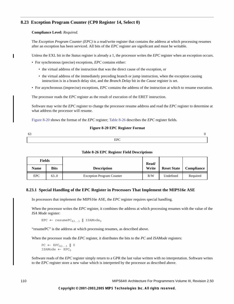
110 MIPS64® Architecture For Programmers Volume III, Revision 2.50
Copyright © 2001-2003,2005 MIPS Technologies Inc. All rights reserved.
8.23 Exception Program Counter (CP0 Register 14, Select 0)
Compliance Level: Required.
The Exception Program Counter (EPC) is a read/write register that contains the address at which processing resumesafter an exception has been serviced. All bits of the EPC register are significant and must be writable.
Unless the EXL bit in the Status register is already a 1, the processor writes the EPC register when an exception occurs.
• For synchronous (precise) exceptions, EPC contains either:
• the virtual address of the instruction that was the direct cause of the exception, or
• the virtual address of the immediately preceding branch or jump instruction, when the exception causinginstruction is in a branch delay slot, and the Branch Delay bit in the Cause register is set.
• For asynchronous (imprecise) exceptions, EPC contains the address of the instruction at which to resume execution.
The processor reads the EPC register as the result of execution of the ERET instruction.
Software may write the EPC register to change the processor resume address and read the EPC register to determine atwhat address the processor will resume.
Figure 8-20 shows the format of the EPC register; Table 8-26 describes the EPC register fields.
8.23.1 Special Handling of the EPC Register in Processors That Implement the MIPS16e ASE
In processors that implement the MIPS16e ASE, the EPC register requires special handling.
When the processor writes the EPC register, it combines the address at which processing resumes with the value of theISA Mode register:
EPC ← resumePC63..1 || ISAMode0
“resumePC” is the address at which processing resumes, as described above.
When the processor reads the EPC register, it distributes the bits to the PC and ISAMode registers:
PC ← EPC63..1 || 0ISAMode ← EPC0
Software reads of the EPC register simply return to a GPR the last value written with no interpretation. Software writesto the EPC register store a new value which is interpreted by the processor as described above.
Figure 8-20 EPC Register Format
63 0
EPC
Table 8-26 EPC Register Field Descriptions
Fields
DescriptionRead/Write Reset State ComplianceName Bits
EPC 63..0 Exception Program Counter R/W Undefined Required
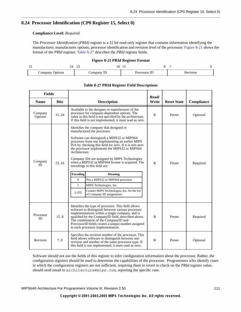
8.24 Processor Identification (CP0 Register 15, Select 0)
MIPS64® Architecture For Programmers Volume III, Revision 2.50 111
Copyright © 2001-2003,2005 MIPS Technologies Inc. All rights reserved.
8.24 Processor Identification (CP0 Register 15, Select 0)
Compliance Level: Required.
The Processor Identification (PRId) register is a 32 bit read-only register that contains information identifying themanufacturer, manufacturer options, processor identification and revision level of the processor. Figure 8-21 shows theformat of the PRId register; Table 8-27 describes the PRId register fields.
Software should not use the fields of this register to infer configuration information about the processor. Rather, theconfiguration registers should be used to determine the capabilities of the processor. Programmers who identify casesin which the configuration registers are not sufficient, requiring them to revert to check on the PRId register value,should send email to [email protected], reporting the specific case.
Figure 8-21 PRId Register Format
31 24 23 16 15 8 7 0
Company Options Company ID Processor ID Revision
Table 8-27 PRId Register Field Descriptions
Fields
DescriptionRead/Write Reset State ComplianceName Bits
CompanyOptions 31..24
Available to the designer or manufacturer of theprocessor for company-dependent options. Thevalue in this field is not specified by the architecture.If this field is not implemented, it must read as zero.
R Preset Optional
CompanyID 23..16
Identifies the company that designed ormanufactured the processor.
Software can distinguish a MIPS32 or MIPS64processor from one implementing an earlier MIPSISA by checking this field for zero. If it is non-zerothe processor implements the MIPS32 or MIPS64Architecture.
Company IDs are assigned by MIPS Technologieswhen a MIPS32 or MIPS64 license is acquired. Theencodings in this field are:
R Preset Required
ProcessorID 15..8
Identifies the type of processor. This field allowssoftware to distinguish between various processorimplementations within a single company, and isqualified by the CompanyID field, described above.The combination of the CompanyID andProcessorID fields creates a unique number assignedto each processor implementation.
R Preset Required
Revision 7..0
Specifies the revision number of the processor. Thisfield allows software to distinguish between onerevision and another of the same processor type. Ifthis field is not implemented, it must read as zero.
R Preset Optional
Encoding Meaning
0 Not a MIPS32 or MIPS64 processor
1 MIPS Technologies, Inc.
2-255Contact MIPS Technologies, Inc. for the listof Company ID assignments
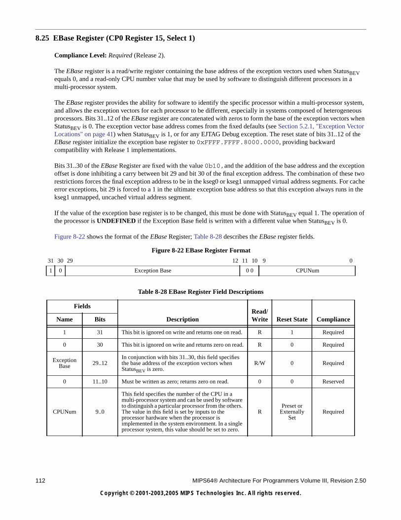
112 MIPS64® Architecture For Programmers Volume III, Revision 2.50
Copyright © 2001-2003,2005 MIPS Technologies Inc. All rights reserved.
8.25 EBase Register (CP0 Register 15, Select 1)
Compliance Level: Required (Release 2).
The EBase register is a read/write register containing the base address of the exception vectors used when StatusBEVequals 0, and a read-only CPU number value that may be used by software to distinguish different processors in amulti-processor system.
The EBase register provides the ability for software to identify the specific processor within a multi-processor system,and allows the exception vectors for each processor to be different, especially in systems composed of heterogeneousprocessors. Bits 31..12 of the EBase register are concatenated with zeros to form the base of the exception vectors whenStatusBEV is 0. The exception vector base address comes from the fixed defaults (see Section 5.2.1, "Exception VectorLocations" on page 41) when StatusBEV is 1, or for any EJTAG Debug exception. The reset state of bits 31..12 of theEBase register initialize the exception base register to 0xFFFF.FFFF.8000.0000, providing backwardcompatibility with Release 1 implementations.
Bits 31..30 of the EBase Register are fixed with the value 0b10,and the addition of the base address and the exceptionoffset is done inhibiting a carry between bit 29 and bit 30 of the final exception address. The combination of these tworestrictions forces the final exception address to be in the kseg0 or kseg1 unmapped virtual address segments. For cacheerror exceptions, bit 29 is forced to a 1 in the ultimate exception base address so that this exception always runs in thekseg1 unmapped, uncached virtual address segment.
If the value of the exception base register is to be changed, this must be done with StatusBEV equal 1. The operation ofthe processor is UNDEFINED if the Exception Base field is written with a different value when StatusBEV is 0.
Figure 8-22 shows the format of the EBase Register; Table 8-28 describes the EBase register fields.
Figure 8-22 EBase Register Format
31 30 29 12 11 10 9 0
1 0 Exception Base 0 0 CPUNum
Table 8-28 EBase Register Field Descriptions
Fields
DescriptionRead/Write Reset State ComplianceName Bits
1 31 This bit is ignored on write and returns one on read. R 1 Required
0 30 This bit is ignored on write and returns zero on read. R 0 Required
ExceptionBase 29..12
In conjunction with bits 31..30, this field specifiesthe base address of the exception vectors whenStatusBEV is zero.
R/W 0 Required
0 11..10 Must be written as zero; returns zero on read. 0 0 Reserved
CPUNum 9..0
This field specifies the number of the CPU in amulti-processor system and can be used by softwareto distinguish a particular processor from the others.The value in this field is set by inputs to theprocessor hardware when the processor isimplemented in the system environment. In a singleprocessor system, this value should be set to zero.
RPreset or
ExternallySet
Required
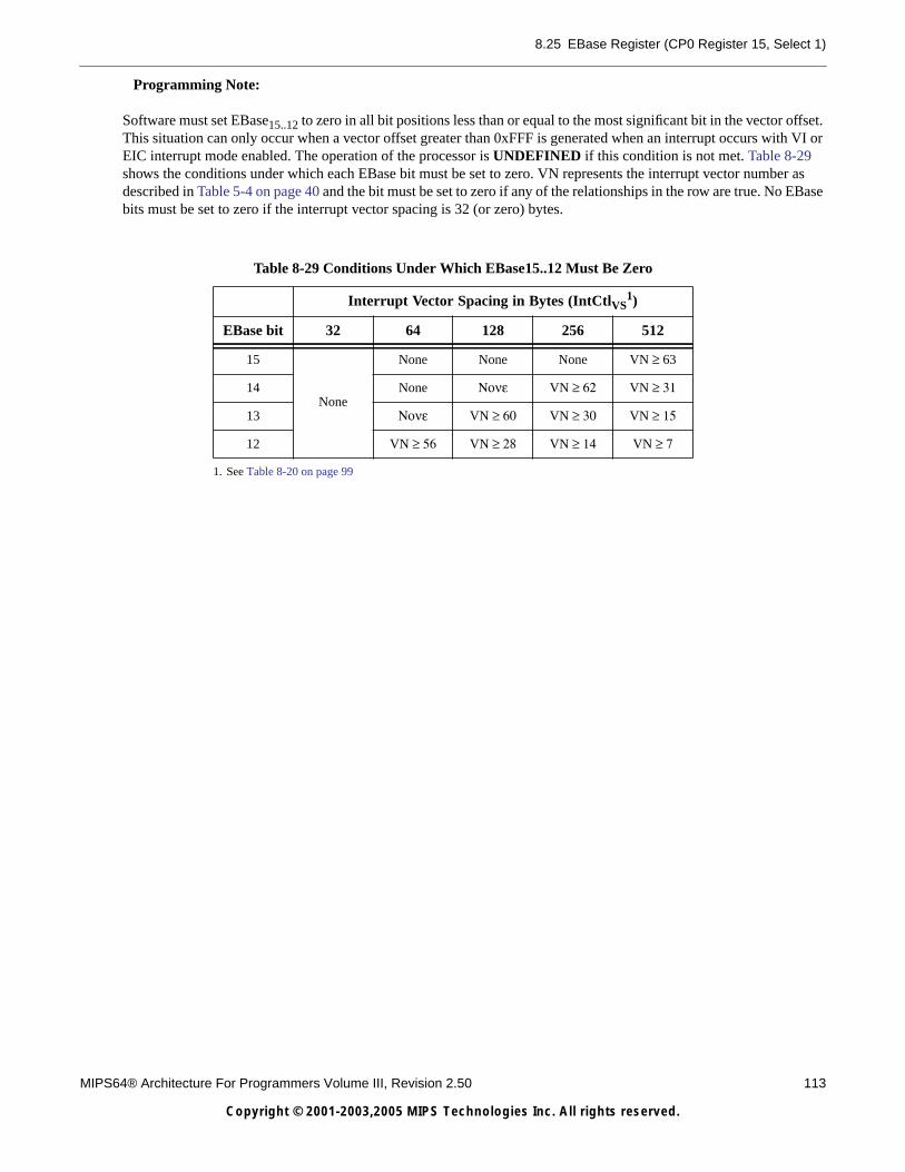
8.25 EBase Register (CP0 Register 15, Select 1)
MIPS64® Architecture For Programmers Volume III, Revision 2.50 113
Copyright © 2001-2003,2005 MIPS Technologies Inc. All rights reserved.
Programming Note:
Software must set EBase15..12 to zero in all bit positions less than or equal to the most significant bit in the vector offset.This situation can only occur when a vector offset greater than 0xFFF is generated when an interrupt occurs with VI orEIC interrupt mode enabled. The operation of the processor is UNDEFINED if this condition is not met. Table 8-29shows the conditions under which each EBase bit must be set to zero. VN represents the interrupt vector number asdescribed in Table 5-4 on page 40 and the bit must be set to zero if any of the relationships in the row are true. No EBasebits must be set to zero if the interrupt vector spacing is 32 (or zero) bytes.
Table 8-29 Conditions Under Which EBase15..12 Must Be Zero
Interrupt Vector Spacing in Bytes (IntCtlVS1)
1. See Table 8-20 on page 99
EBase bit 32 64 128 256 512
15
None
None None None VN ≥ 63
14 None Νονε VN ≥ 62 VN ≥ 31
13 Νονε VN ≥ 60 VN ≥ 30 VN ≥ 15
12 VN ≥ 56 VN ≥ 28 VN ≥ 14 VN ≥ 7
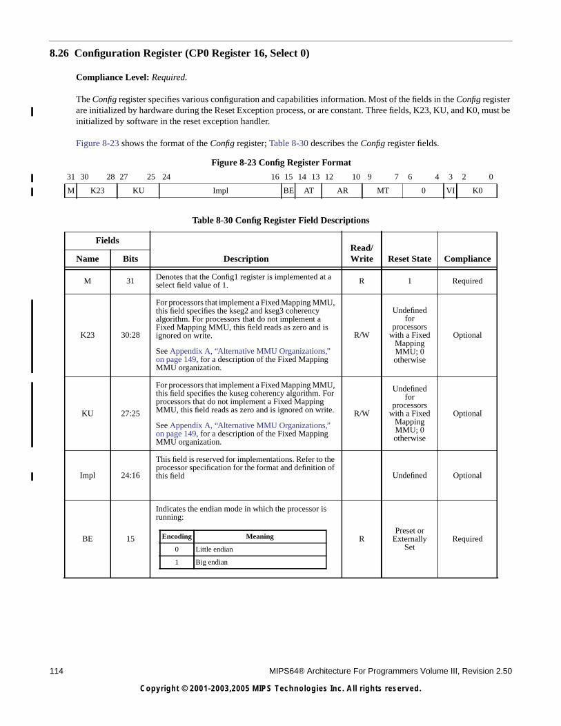
114 MIPS64® Architecture For Programmers Volume III, Revision 2.50
Copyright © 2001-2003,2005 MIPS Technologies Inc. All rights reserved.
8.26 Configuration Register (CP0 Register 16, Select 0)
Compliance Level: Required.
The Config register specifies various configuration and capabilities information. Most of the fields in the Config registerare initialized by hardware during the Reset Exception process, or are constant. Three fields, K23, KU, and K0, must beinitialized by software in the reset exception handler.
Figure 8-23 shows the format of the Config register; Table 8-30 describes the Config register fields.
Figure 8-23 Config Register Format
31 30 28 27 25 24 16 15 14 13 12 10 9 7 6 4 3 2 0
M K23 KU Impl BE AT AR MT 0 VI K0
Table 8-30 Config Register Field Descriptions
Fields
DescriptionRead/Write Reset State ComplianceName Bits
M 31 Denotes that the Config1 register is implemented at aselect field value of 1. R 1 Required
K23 30:28
For processors that implement a Fixed Mapping MMU,this field specifies the kseg2 and kseg3 coherencyalgorithm. For processors that do not implement aFixed Mapping MMU, this field reads as zero and isignored on write.
See Appendix A, “Alternative MMU Organizations,”on page 149, for a description of the Fixed MappingMMU organization.
R/W
Undefinedfor
processorswith a Fixed
MappingMMU; 0otherwise
Optional
KU 27:25
For processors that implement a Fixed Mapping MMU,this field specifies the kuseg coherency algorithm. Forprocessors that do not implement a Fixed MappingMMU, this field reads as zero and is ignored on write.
See Appendix A, “Alternative MMU Organizations,”on page 149, for a description of the Fixed MappingMMU organization.
R/W
Undefinedfor
processorswith a Fixed
MappingMMU; 0otherwise
Optional
Impl 24:16
This field is reserved for implementations. Refer to theprocessor specification for the format and definition ofthis field Undefined Optional
BE 15
Indicates the endian mode in which the processor isrunning:
RPreset or
ExternallySet
RequiredEncoding Meaning
0 Little endian
1 Big endian
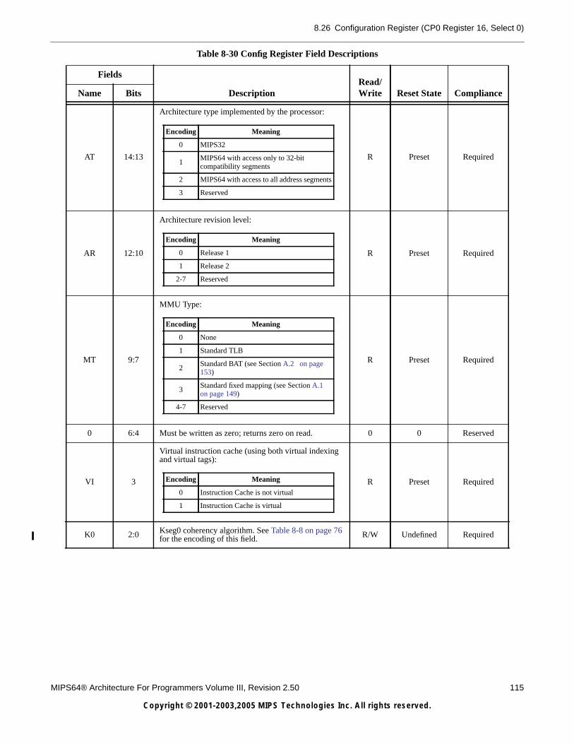
8.26 Configuration Register (CP0 Register 16, Select 0)
MIPS64® Architecture For Programmers Volume III, Revision 2.50 115
Copyright © 2001-2003,2005 MIPS Technologies Inc. All rights reserved.
AT 14:13
Architecture type implemented by the processor:
R Preset Required
AR 12:10
Architecture revision level:
R Preset Required
MT 9:7
MMU Type:
R Preset Required
0 6:4 Must be written as zero; returns zero on read. 0 0 Reserved
VI 3
Virtual instruction cache (using both virtual indexingand virtual tags):
R Preset Required
K0 2:0 Kseg0 coherency algorithm. See Table 8-8 on page 76for the encoding of this field. R/W Undefined Required
Table 8-30 Config Register Field Descriptions
Fields
DescriptionRead/Write Reset State ComplianceName Bits
Encoding Meaning
0 MIPS32
1MIPS64 with access only to 32-bitcompatibility segments
2 MIPS64 with access to all address segments
3 Reserved
Encoding Meaning
0 Release 1
1 Release 2
2-7 Reserved
Encoding Meaning
0 None
1 Standard TLB
2Standard BAT (see Section A.2 on page153)
3Standard fixed mapping (see Section A.1on page 149)
4-7 Reserved
Encoding Meaning
0 Instruction Cache is not virtual
1 Instruction Cache is virtual
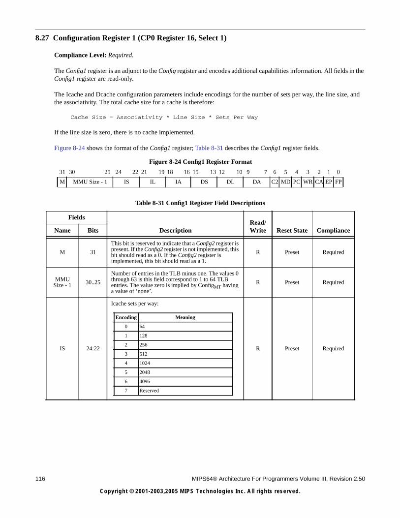
116 MIPS64® Architecture For Programmers Volume III, Revision 2.50
Copyright © 2001-2003,2005 MIPS Technologies Inc. All rights reserved.
8.27 Configuration Register 1 (CP0 Register 16, Select 1)
Compliance Level: Required.
The Config1 register is an adjunct to the Config register and encodes additional capabilities information. All fields in theConfig1 register are read-only.
The Icache and Dcache configuration parameters include encodings for the number of sets per way, the line size, andthe associativity. The total cache size for a cache is therefore:
Cache Size = Associativity * Line Size * Sets Per Way
If the line size is zero, there is no cache implemented.
Figure 8-24 shows the format of the Config1 register; Table 8-31 describes the Config1 register fields.
Figure 8-24 Config1 Register Format
31 30 25 24 22 21 19 18 16 15 13 12 10 9 7 6 5 4 3 2 1 0
M MMU Size - 1 IS IL IA DS DL DA C2 MD PC WR CA EP FP
Table 8-31 Config1 Register Field Descriptions
Fields
DescriptionRead/Write Reset State ComplianceName Bits
M 31
This bit is reserved to indicate that a Config2 register ispresent. If the Config2 register is not implemented, thisbit should read as a 0. If the Config2 register isimplemented, this bit should read as a 1.
R Preset Required
MMUSize - 1 30..25
Number of entries in the TLB minus one. The values 0through 63 is this field correspond to 1 to 64 TLBentries. The value zero is implied by ConfigMT havinga value of ‘none’.
R Preset Required
IS 24:22
Icache sets per way:
R Preset Required
Encoding Meaning
0 64
1 128
2 256
3 512
4 1024
5 2048
6 4096
7 Reserved
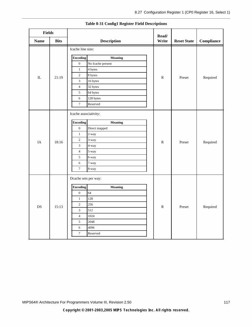
8.27 Configuration Register 1 (CP0 Register 16, Select 1)
MIPS64® Architecture For Programmers Volume III, Revision 2.50 117
Copyright © 2001-2003,2005 MIPS Technologies Inc. All rights reserved.
IL 21:19
Icache line size:
R Preset Required
IA 18:16
Icache associativity:
R Preset Required
DS 15:13
Dcache sets per way:
R Preset Required
Table 8-31 Config1 Register Field Descriptions
Fields
DescriptionRead/Write Reset State ComplianceName Bits
Encoding Meaning
0 No Icache present
1 4 bytes
2 8 bytes
3 16 bytes
4 32 bytes
5 64 bytes
6 128 bytes
7 Reserved
Encoding Meaning
0 Direct mapped
1 2-way
2 3-way
3 4-way
4 5-way
5 6-way
6 7-way
7 8-way
Encoding Meaning
0 64
1 128
2 256
3 512
4 1024
5 2048
6 4096
7 Reserved
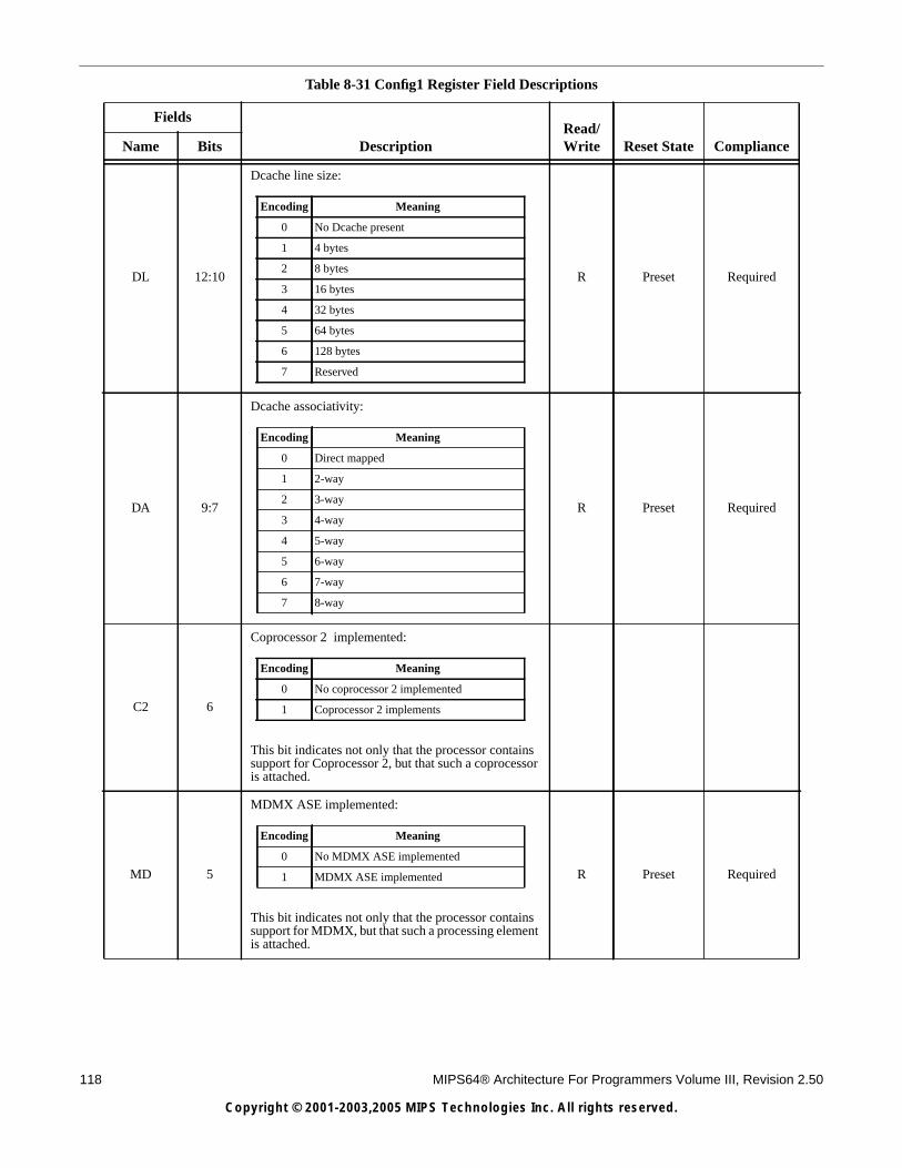
118 MIPS64® Architecture For Programmers Volume III, Revision 2.50
Copyright © 2001-2003,2005 MIPS Technologies Inc. All rights reserved.
DL 12:10
Dcache line size:
R Preset Required
DA 9:7
Dcache associativity:
R Preset Required
C2 6
Coprocessor 2 implemented:
This bit indicates not only that the processor containssupport for Coprocessor 2, but that such a coprocessoris attached.
MD 5
MDMX ASE implemented:
This bit indicates not only that the processor containssupport for MDMX, but that such a processing elementis attached.
R Preset Required
Table 8-31 Config1 Register Field Descriptions
Fields
DescriptionRead/Write Reset State ComplianceName Bits
Encoding Meaning
0 No Dcache present
1 4 bytes
2 8 bytes
3 16 bytes
4 32 bytes
5 64 bytes
6 128 bytes
7 Reserved
Encoding Meaning
0 Direct mapped
1 2-way
2 3-way
3 4-way
4 5-way
5 6-way
6 7-way
7 8-way
Encoding Meaning
0 No coprocessor 2 implemented
1 Coprocessor 2 implements
Encoding Meaning
0 No MDMX ASE implemented
1 MDMX ASE implemented
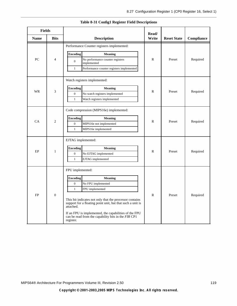
8.27 Configuration Register 1 (CP0 Register 16, Select 1)
MIPS64® Architecture For Programmers Volume III, Revision 2.50 119
Copyright © 2001-2003,2005 MIPS Technologies Inc. All rights reserved.
PC 4
Performance Counter registers implemented:
R Preset Required
WR 3
Watch registers implemented:
R Preset Required
CA 2
Code compression (MIPS16e) implemented:
R Preset Required
EP 1
EJTAG implemented:
R Preset Required
FP 0
FPU implemented:
This bit indicates not only that the processor containssupport for a floating point unit, but that such a unit isattached.
If an FPU is implemented, the capabilities of the FPUcan be read from the capability bits in the FIR CP1register.
R Preset Required
Table 8-31 Config1 Register Field Descriptions
Fields
DescriptionRead/Write Reset State ComplianceName Bits
Encoding Meaning
0No performance counter registersimplemented
1 Performance counter registers implemented
Encoding Meaning
0 No watch registers implemented
1 Watch registers implemented
Encoding Meaning
0 MIPS16e not implemented
1 MIPS16e implemented
Encoding Meaning
0 No EJTAG implemented
1 EJTAG implemented
Encoding Meaning
0 No FPU implemented
1 FPU implemented
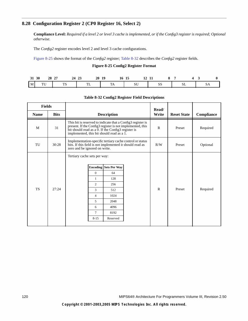
120 MIPS64® Architecture For Programmers Volume III, Revision 2.50
Copyright © 2001-2003,2005 MIPS Technologies Inc. All rights reserved.
8.28 Configuration Register 2 (CP0 Register 16, Select 2)
Compliance Level: Required if a level 2 or level 3 cache is implemented, or if the Config3 register is required; Optionalotherwise.
The Config2 register encodes level 2 and level 3 cache configurations.
Figure 8-25 shows the format of the Config2 register; Table 8-32 describes the Config2 register fields.
Figure 8-25 Config2 Register Format
31 30 28 27 24 23 20 19 16 15 12 11 8 7 4 3 0
M TU TS TL TA SU SS SL SA
Table 8-32 Config2 Register Field Descriptions
Fields
DescriptionRead/Write Reset State ComplianceName Bits
M 31
This bit is reserved to indicate that a Config3 register ispresent. If the Config3 register is not implemented, thisbit should read as a 0. If the Config3 register isimplemented, this bit should read as a 1.
R Preset Required
TU 30:28Implementation-specific tertiary cache control or statusbits. If this field is not implemented it should read aszero and be ignored on write.
R/W Preset Optional
TS 27:24
Tertiary cache sets per way:
R Preset Required
Encoding Sets Per Way
0 64
1 128
2 256
3 512
4 1024
5 2048
6 4096
7 8192
8-15 Reserved
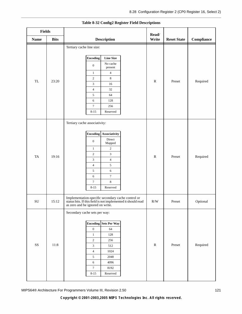
8.28 Configuration Register 2 (CP0 Register 16, Select 2)
MIPS64® Architecture For Programmers Volume III, Revision 2.50 121
Copyright © 2001-2003,2005 MIPS Technologies Inc. All rights reserved.
TL 23:20
Tertiary cache line size:
R Preset Required
TA 19:16
Tertiary cache associativity:
R Preset Required
SU 15:12Implementation-specific secondary cache control orstatus bits. If this field is not implemented it should readas zero and be ignored on write.
R/W Preset Optional
SS 11:8
Secondary cache sets per way:
R Preset Required
Table 8-32 Config2 Register Field Descriptions
Fields
DescriptionRead/Write Reset State ComplianceName Bits
Encoding Line Size
0No cachepresent
1 4
2 8
3 16
4 32
5 64
6 128
7 256
8-15 Reserved
Encoding Associativity
0Direct
Mapped
1 2
2 3
3 4
4 5
5 6
6 7
7 8
8-15 Reserved
Encoding Sets Per Way
0 64
1 128
2 256
3 512
4 1024
5 2048
6 4096
7 8192
8-15 Reserved
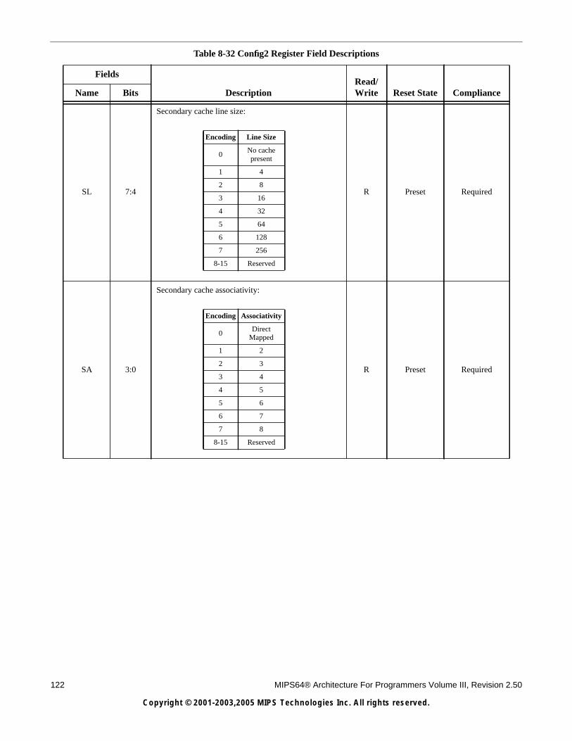
122 MIPS64® Architecture For Programmers Volume III, Revision 2.50
Copyright © 2001-2003,2005 MIPS Technologies Inc. All rights reserved.
SL 7:4
Secondary cache line size:
R Preset Required
SA 3:0
Secondary cache associativity:
R Preset Required
Table 8-32 Config2 Register Field Descriptions
Fields
DescriptionRead/Write Reset State ComplianceName Bits
Encoding Line Size
0No cachepresent
1 4
2 8
3 16
4 32
5 64
6 128
7 256
8-15 Reserved
Encoding Associativity
0Direct
Mapped
1 2
2 3
3 4
4 5
5 6
6 7
7 8
8-15 Reserved
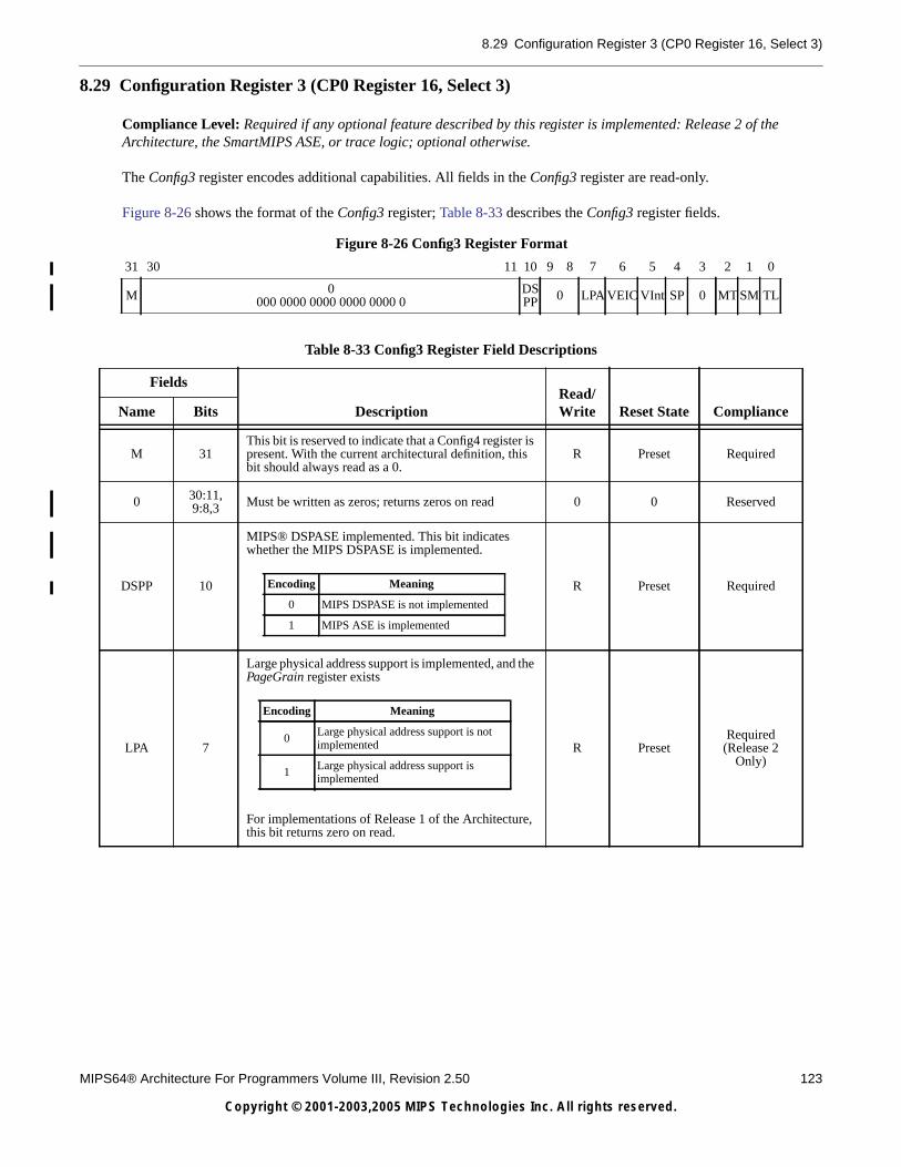
8.29 Configuration Register 3 (CP0 Register 16, Select 3)
MIPS64® Architecture For Programmers Volume III, Revision 2.50 123
Copyright © 2001-2003,2005 MIPS Technologies Inc. All rights reserved.
8.29 Configuration Register 3 (CP0 Register 16, Select 3)
Compliance Level: Required if any optional feature described by this register is implemented: Release 2 of theArchitecture, the SmartMIPS ASE, or trace logic; optional otherwise.
The Config3 register encodes additional capabilities. All fields in the Config3 register are read-only.
Figure 8-26 shows the format of the Config3 register; Table 8-33 describes the Config3 register fields.
Figure 8-26 Config3 Register Format
31 30 11 10 9 8 7 6 5 4 3 2 1 0
M 0000 0000 0000 0000 0000 0
DSPP 0 LPA VEIC VInt SP 0 MT SM TL
Table 8-33 Config3 Register Field Descriptions
Fields
DescriptionRead/Write Reset State ComplianceName Bits
M 31This bit is reserved to indicate that a Config4 register ispresent. With the current architectural definition, thisbit should always read as a 0.
R Preset Required
0 30:11,9:8,3 Must be written as zeros; returns zeros on read 0 0 Reserved
DSPP 10
MIPS® DSPASE implemented. This bit indicateswhether the MIPS DSPASE is implemented.
R Preset Required
LPA 7
Large physical address support is implemented, and thePageGrain register exists
For implementations of Release 1 of the Architecture,this bit returns zero on read.
R PresetRequired
(Release 2Only)
Encoding Meaning
0 MIPS DSPASE is not implemented
1 MIPS ASE is implemented
Encoding Meaning
0Large physical address support is notimplemented
1Large physical address support isimplemented
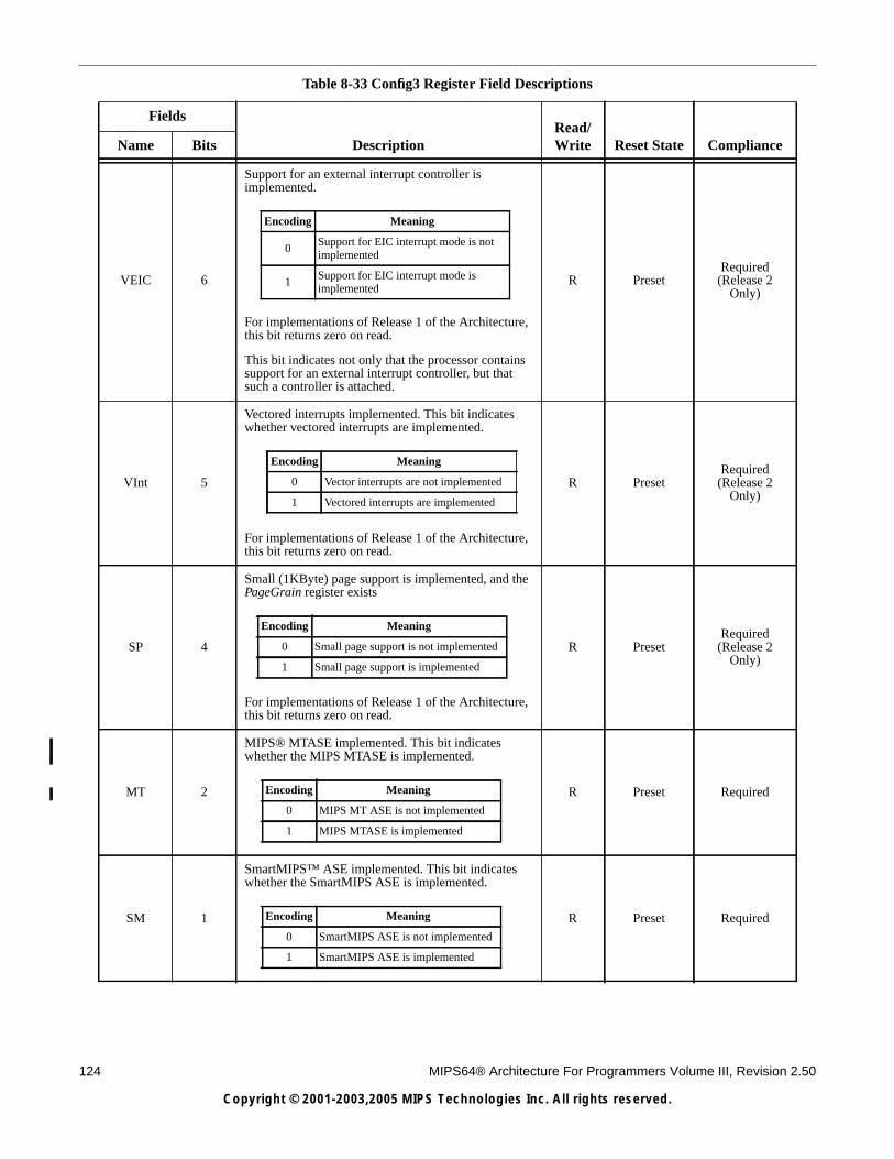
124 MIPS64® Architecture For Programmers Volume III, Revision 2.50
Copyright © 2001-2003,2005 MIPS Technologies Inc. All rights reserved.
VEIC 6
Support for an external interrupt controller isimplemented.
For implementations of Release 1 of the Architecture,this bit returns zero on read.
This bit indicates not only that the processor containssupport for an external interrupt controller, but thatsuch a controller is attached.
R PresetRequired
(Release 2Only)
VInt 5
Vectored interrupts implemented. This bit indicateswhether vectored interrupts are implemented.
For implementations of Release 1 of the Architecture,this bit returns zero on read.
R PresetRequired
(Release 2Only)
SP 4
Small (1KByte) page support is implemented, and thePageGrain register exists
For implementations of Release 1 of the Architecture,this bit returns zero on read.
R PresetRequired
(Release 2Only)
MT 2
MIPS® MTASE implemented. This bit indicateswhether the MIPS MTASE is implemented.
R Preset Required
SM 1
SmartMIPS™ ASE implemented. This bit indicateswhether the SmartMIPS ASE is implemented.
R Preset Required
Table 8-33 Config3 Register Field Descriptions
Fields
DescriptionRead/Write Reset State ComplianceName Bits
Encoding Meaning
0Support for EIC interrupt mode is notimplemented
1Support for EIC interrupt mode isimplemented
Encoding Meaning
0 Vector interrupts are not implemented
1 Vectored interrupts are implemented
Encoding Meaning
0 Small page support is not implemented
1 Small page support is implemented
Encoding Meaning
0 MIPS MT ASE is not implemented
1 MIPS MTASE is implemented
Encoding Meaning
0 SmartMIPS ASE is not implemented
1 SmartMIPS ASE is implemented
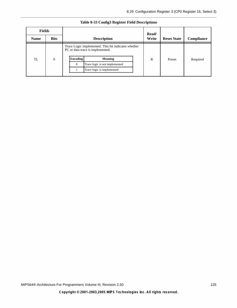
8.29 Configuration Register 3 (CP0 Register 16, Select 3)
MIPS64® Architecture For Programmers Volume III, Revision 2.50 125
Copyright © 2001-2003,2005 MIPS Technologies Inc. All rights reserved.
TL 0
Trace Logic implemented. This bit indicates whetherPC or data trace is implemented.
R Preset Required
Table 8-33 Config3 Register Field Descriptions
Fields
DescriptionRead/Write Reset State ComplianceName Bits
Encoding Meaning
0 Trace logic is not implemented
1 Trace logic is implemented
126 MIPS64® Architecture For Programmers Volume III, Revision 2.50
Copyright © 2001-2003,2005 MIPS Technologies Inc. All rights reserved.
8.30 Reserved for Implementations (CP0 Register 16, Selects 6 and 7)
Compliance Level: Optional: Implementation Dependent.
CP0 register 16, Selects 6 and 7 are reserved for implementation dependent use and is not defined by the architecture.In order to use CP0 register 16, Selects 6 and 7, it is not necessary to implement CP0 register 16, Selects 2 through 5only to set the M bit in each of these registers. That is, if the Config2 and Config3 registers are not needed for theimplementation, they need not be implemented just to provide the M bits.
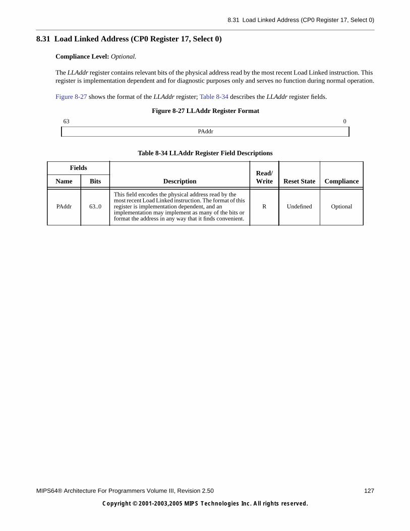
8.31 Load Linked Address (CP0 Register 17, Select 0)
MIPS64® Architecture For Programmers Volume III, Revision 2.50 127
Copyright © 2001-2003,2005 MIPS Technologies Inc. All rights reserved.
8.31 Load Linked Address (CP0 Register 17, Select 0)
Compliance Level: Optional.
The LLAddr register contains relevant bits of the physical address read by the most recent Load Linked instruction. Thisregister is implementation dependent and for diagnostic purposes only and serves no function during normal operation.
Figure 8-27 shows the format of the LLAddr register; Table 8-34 describes the LLAddr register fields.
Figure 8-27 LLAddr Register Format
63 0
PAddr
Table 8-34 LLAddr Register Field Descriptions
Fields
DescriptionRead/Write Reset State ComplianceName Bits
PAddr 63..0
This field encodes the physical address read by themost recent Load Linked instruction. The format of thisregister is implementation dependent, and animplementation may implement as many of the bits orformat the address in any way that it finds convenient.
R Undefined Optional
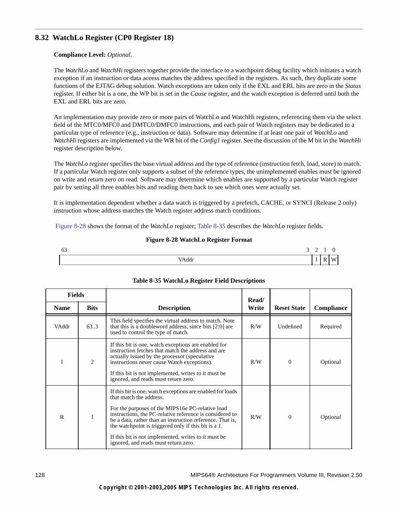
128 MIPS64® Architecture For Programmers Volume III, Revision 2.50
Copyright © 2001-2003,2005 MIPS Technologies Inc. All rights reserved.
8.32 WatchLo Register (CP0 Register 18)
Compliance Level: Optional.
The WatchLo and WatchHi registers together provide the interface to a watchpoint debug facility which initiates a watchexception if an instruction or data access matches the address specified in the registers. As such, they duplicate somefunctions of the EJTAG debug solution. Watch exceptions are taken only if the EXL and ERL bits are zero in the Statusregister. If either bit is a one, the WP bit is set in the Cause register, and the watch exception is deferred until both theEXL and ERL bits are zero.
An implementation may provide zero or more pairs of WatchLo and WatchHi registers, referencing them via the selectfield of the MTC0/MFC0 and DMTC0/DMFC0 instructions, and each pair of Watch registers may be dedicated to aparticular type of reference (e.g., instruction or data). Software may determine if at least one pair of WatchLo andWatchHi registers are implemented via the WR bit of the Config1 register. See the discussion of the M bit in the WatchHiregister description below.
The WatchLo register specifies the base virtual address and the type of reference (instruction fetch, load, store) to match.If a particular Watch register only supports a subset of the reference types, the unimplemented enables must be ignoredon write and return zero on read. Software may determine which enables are supported by a particular Watch registerpair by setting all three enables bits and reading them back to see which ones were actually set.
It is implementation dependent whether a data watch is triggered by a prefetch, CACHE, or SYNCI (Release 2 only)instruction whose address matches the Watch register address match conditions.
Figure 8-28 shows the format of the WatchLo register; Table 8-35 describes the WatchLo register fields.
Figure 8-28 WatchLo Register Format
63 3 2 1 0
VAddr I R W
Table 8-35 WatchLo Register Field Descriptions
Fields
DescriptionRead/Write Reset State ComplianceName Bits
VAddr 63..3This field specifies the virtual address to match. Notethat this is a doubleword address, since bits [2:0] areused to control the type of match.
R/W Undefined Required
I 2
If this bit is one, watch exceptions are enabled forinstruction fetches that match the address and areactually issued by the processor (speculativeinstructions never cause Watch exceptions).
If this bit is not implemented, writes to it must beignored, and reads must return zero.
R/W 0 Optional
R 1
If this bit is one, watch exceptions are enabled for loadsthat match the address.
For the purposes of the MIPS16e PC-relative loadinstructions, the PC-relative reference is considered tobe a data, rather than an instruction reference. That is,the watchpoint is triggered only if this bit is a 1.
If this bit is not implemented, writes to it must beignored, and reads must return zero.
R/W 0 Optional
8.32 WatchLo Register (CP0 Register 18)
MIPS64® Architecture For Programmers Volume III, Revision 2.50 129
Copyright © 2001-2003,2005 MIPS Technologies Inc. All rights reserved.
W 0
If this bit is one, watch exceptions are enabled forstores that match the address.
If this bit is not implemented, writes to it must beignored, and reads must return zero.
R/W 0 Optional
Table 8-35 WatchLo Register Field Descriptions
Fields
DescriptionRead/Write Reset State ComplianceName Bits
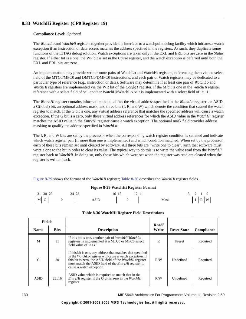
130 MIPS64® Architecture For Programmers Volume III, Revision 2.50
Copyright © 2001-2003,2005 MIPS Technologies Inc. All rights reserved.
8.33 WatchHi Register (CP0 Register 19)
Compliance Level: Optional.
The WatchLo and WatchHi registers together provide the interface to a watchpoint debug facility which initiates a watchexception if an instruction or data access matches the address specified in the registers. As such, they duplicate somefunctions of the EJTAG debug solution. Watch exceptions are taken only if the EXL and ERL bits are zero in the Statusregister. If either bit is a one, the WP bit is set in the Cause register, and the watch exception is deferred until both theEXL and ERL bits are zero.
An implementation may provide zero or more pairs of WatchLo and WatchHi registers, referencing them via the selectfield of the MTC0/MFC0 and DMTC0/DMFC0 instructions, and each pair of Watch registers may be dedicated to aparticular type of reference (e.g., instruction or data). Software may determine if at least one pair of WatchLo andWatchHi registers are implemented via the WR bit of the Config1 register. If the M bit is one in the WatchHi registerreference with a select field of ‘n’, another WatchHi/WatchLo pair is implemented with a select field of ‘n+1’.
The WatchHi register contains information that qualifies the virtual address specified in the WatchLo register: an ASID,a G(lobal) bit, an optional address mask, and three bits (I, R, and W) which denote the condition that caused the watchregister to match. If the G bit is one, any virtual address reference that matches the specified address will cause a watchexception. If the G bit is a zero, only those virtual address references for which the ASID value in the WatchHi registermatches the ASID value in the EntryHi register cause a watch exception. The optional mask field provides addressmasking to qualify the address specified in WatchLo.
The I, R, and W bits are set by the processor when the corresponding watch register condition is satisfied and indicatewhich watch register pair (if more than one is implemented) and which condition matched. When set by the processor,each of these bits remain set until cleared by software. All three bits are “write one to clear”, such that software mustwrite a one to the bit in order to clear its value. The typical way to do this is to write the value read from the WatchHiregister back to WatchHi. In doing so, only those bits which were set when the register was read are cleared when theregister is written back.
Figure 8-29 shows the format of the WatchHi register; Table 8-36 describes the WatchHi register fields.
Figure 8-29 WatchHi Register Format
31 30 29 24 23 16 15 12 11 3 2 1 0
M G 0 ASID 0 Mask I R W
Table 8-36 WatchHi Register Field Descriptions
Fields
DescriptionRead/Write Reset State ComplianceName Bits
M 31If this bit is one, another pair of WatchHi/WatchLoregisters is implemented at a MTC0 or MFC0 selectfield value of ‘n+1’
R Preset Required
G 30
If this bit is one, any address that matches that specifiedin the WatchLo register will cause a watch exception. Ifthis bit is zero, the ASID field of the WatchHi registermust match the ASID field of the EntryHi register tocause a watch exception.
R/W Undefined Required
ASID 23..16ASID value which is required to match that in theEntryHi register if the G bit is zero in the WatchHiregister.
R/W Undefined Required
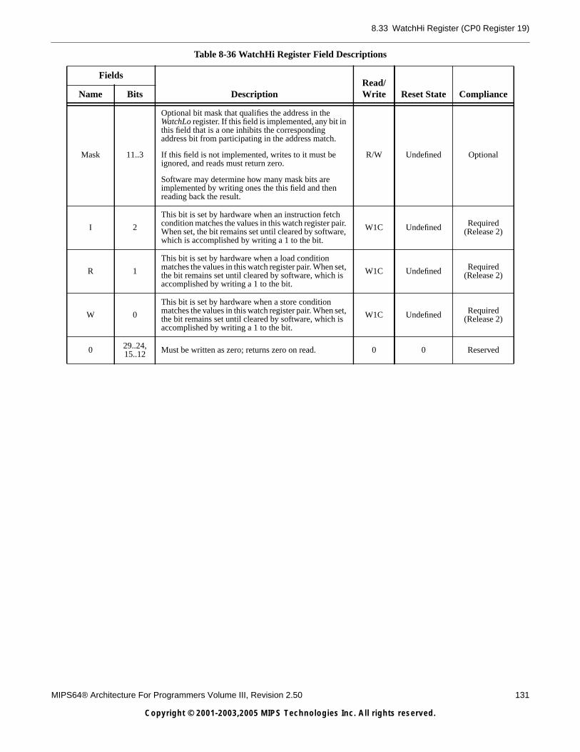
8.33 WatchHi Register (CP0 Register 19)
MIPS64® Architecture For Programmers Volume III, Revision 2.50 131
Copyright © 2001-2003,2005 MIPS Technologies Inc. All rights reserved.
Mask 11..3
Optional bit mask that qualifies the address in theWatchLo register. If this field is implemented, any bit inthis field that is a one inhibits the correspondingaddress bit from participating in the address match.
If this field is not implemented, writes to it must beignored, and reads must return zero.
Software may determine how many mask bits areimplemented by writing ones the this field and thenreading back the result.
R/W Undefined Optional
I 2
This bit is set by hardware when an instruction fetchcondition matches the values in this watch register pair.When set, the bit remains set until cleared by software,which is accomplished by writing a 1 to the bit.
W1C Undefined Required(Release 2)
R 1
This bit is set by hardware when a load conditionmatches the values in this watch register pair. When set,the bit remains set until cleared by software, which isaccomplished by writing a 1 to the bit.
W1C Undefined Required(Release 2)
W 0
This bit is set by hardware when a store conditionmatches the values in this watch register pair. When set,the bit remains set until cleared by software, which isaccomplished by writing a 1 to the bit.
W1C Undefined Required(Release 2)
0 29..24,15..12 Must be written as zero; returns zero on read. 0 0 Reserved
Table 8-36 WatchHi Register Field Descriptions
Fields
DescriptionRead/Write Reset State ComplianceName Bits
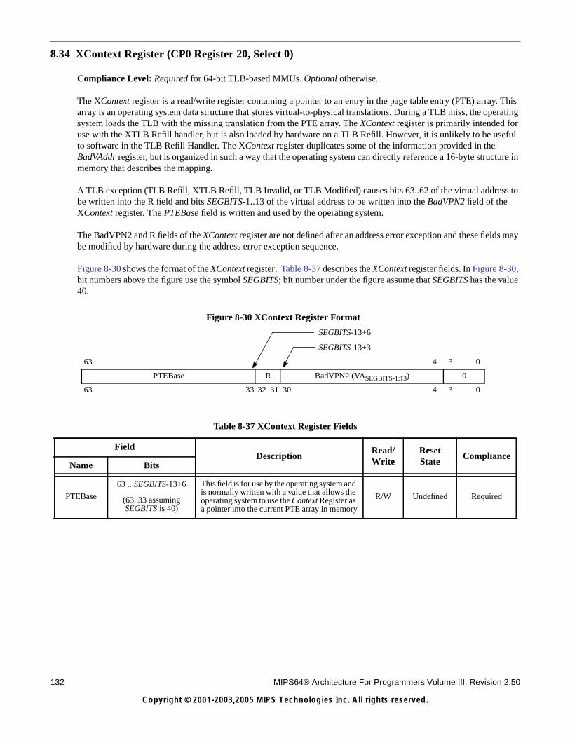
132 MIPS64® Architecture For Programmers Volume III, Revision 2.50
Copyright © 2001-2003,2005 MIPS Technologies Inc. All rights reserved.
8.34 XContext Register (CP0 Register 20, Select 0)
Compliance Level: Required for 64-bit TLB-based MMUs. Optional otherwise.
The XContext register is a read/write register containing a pointer to an entry in the page table entry (PTE) array. Thisarray is an operating system data structure that stores virtual-to-physical translations. During a TLB miss, the operatingsystem loads the TLB with the missing translation from the PTE array. The XContext register is primarily intended foruse with the XTLB Refill handler, but is also loaded by hardware on a TLB Refill. However, it is unlikely to be usefulto software in the TLB Refill Handler. The XContext register duplicates some of the information provided in theBadVAddr register, but is organized in such a way that the operating system can directly reference a 16-byte structure inmemory that describes the mapping.
A TLB exception (TLB Refill, XTLB Refill, TLB Invalid, or TLB Modified) causes bits 63..62 of the virtual address tobe written into the R field and bits SEGBITS-1..13 of the virtual address to be written into the BadVPN2 field of theXContext register. The PTEBase field is written and used by the operating system.
The BadVPN2 and R fields of the XContext register are not defined after an address error exception and these fields maybe modified by hardware during the address error exception sequence.
Figure 8-30 shows the format of the XContext register; Table 8-37 describes the XContext register fields. In Figure 8-30,bit numbers above the figure use the symbol SEGBITS; bit number under the figure assume that SEGBITS has the value40.
Table 8-37 XContext Register Fields
FieldDescription
Read/Write
ResetState
ComplianceName Bits
PTEBase
63 .. SEGBITS-13+6
(63..33 assumingSEGBITS is 40)
This field is for use by the operating system andis normally written with a value that allows theoperating system to use the Context Register asa pointer into the current PTE array in memory
R/W Undefined Required
Figure 8-30 XContext Register Format
SEGBITS-13+6
SEGBITS-13+3
63 4 3 0
PTEBase R BadVPN2 (VASEGBITS-1:13) 0
63 33 32 31 30 4 3 0
8.34 XContext Register (CP0 Register 20, Select 0)
MIPS64® Architecture For Programmers Volume III, Revision 2.50 133
Copyright © 2001-2003,2005 MIPS Technologies Inc. All rights reserved.
R
SEGBITS-13+5 ..SEGBITS-13+4
(32..31 assumingSEGBITS is 40)
The Region field contains bits 63..62 of thevirtual address.
For processors implementing ConfigAT = 1(access to 32-bit compatibility segments only),only the 0b00 and 0b11 values are supplied bythe processor on an exception.
R Undefined Required
BadVPN2
SEGBITS-13+3 .. 4
(30..4 assumingSEGBITS is 40)
The Bad Virtual Page Number/2 field is writtenby hardware on a miss. It contains bitsVASEGBITS-1..13 of the virtual address thatmissed.
R Undefined Required
0 3..0 Must be written as zero; returns zero on read. 0 0 Reserved
Table 8-37 XContext Register Fields
FieldDescription
Read/Write
ResetState
ComplianceName Bits
Encoding Meaning
0b00 xuseg
0b01
xsseg: supervisor address region. IfSupervisor Mode is notimplemented, this encoding isreserved
0b10 Reserved
0b11 xkseg
134 MIPS64® Architecture For Programmers Volume III, Revision 2.50
Copyright © 2001-2003,2005 MIPS Technologies Inc. All rights reserved.
8.35 Reserved for Implementations (CP0 Register 22, all Select values)
Compliance Level: Optional: Implementation Dependent.
CP0 register 22 is reserved for implementation dependent use and is not defined by the architecture.
8.36 Debug Register (CP0 Register 23)
MIPS64® Architecture For Programmers Volume III, Revision 2.50 135
Copyright © 2001-2003,2005 MIPS Technologies Inc. All rights reserved.
8.36 Debug Register (CP0 Register 23)
Compliance Level: Optional.
The Debug register is part of the EJTAG specification. Refer to that specification for the format and description of thisregister.
136 MIPS64® Architecture For Programmers Volume III, Revision 2.50
Copyright © 2001-2003,2005 MIPS Technologies Inc. All rights reserved.
8.37 DEPC Register (CP0 Register 24)
Compliance Level: Optional.
The DEPC register is a read-write register that contains the address at which processing resumes after a debug exceptionhas been serviced. It is part of the EJTAG specification and the reader is referred there for the format and description ofthe register. All bits of the DEPC register are significant and must be writable.
When a debug exception occurs, the processor writes the DEPC register with.
• the virtual address of the instruction that was the direct cause of the exception, or
• the virtual address of the immediately preceding branch or jump instruction, when the exception causing instructionis in a branch delay slot, and the Branch Delay bit in the Cause register is set.
The processor reads the DEPC register as the result of execution of the DERET instruction.
Software may write the EEPC register to change the processor resume address and read the DEPC register to determineat what address the processor will resume.
8.37.1 Special Handling of the DEPC Register in Processors That Implement the MIPS16e ASE
In processors that implement the MIPS16e ASE, the DEPC register requires special handling.
When the processor writes the DEPC register, it combines the address at which processing resumes with the value of theISA Mode register:
DEPC ← resumePC63..1 || ISAMode0
“resumePC” is the address at which processing resumes, as described above.
When the processor reads the DEPC register, it distributes the bits to the PC and ISAMode registers:
PC ← DEPC63..1 || 0ISAMode ← DEPC0
Software reads of the DEPC register simply return to a GPR the last value written with no interpretation. Software writesto the DEPC register store a new value which is interpreted by the processor as described above.
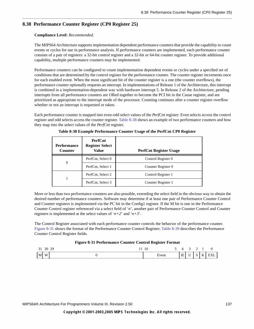
8.38 Performance Counter Register (CP0 Register 25)
MIPS64® Architecture For Programmers Volume III, Revision 2.50 137
Copyright © 2001-2003,2005 MIPS Technologies Inc. All rights reserved.
8.38 Performance Counter Register (CP0 Register 25)
Compliance Level: Recommended.
The MIPS64 Architecture supports implementation dependent performance counters that provide the capability to countevents or cycles for use in performance analysis. If performance counters are implemented, each performance counterconsists of a pair of registers: a 32-bit control register and a 32-bit or 64-bit counter register. To provide additionalcapability, multiple performance counters may be implemented.
Performance counters can be configured to count implementation dependent events or cycles under a specified set ofconditions that are determined by the control register for the performance counter. The counter register increments oncefor each enabled event. When the most significant bit of the counter register is a one (the counter overflows), theperformance counter optionally requests an interrupt. In implementations of Release 1 of the Architecture, this interruptis combined in a implementation-dependent way with hardware interrupt 5. In Release 2 of the Architecture, pendinginterrupts from all performance counters are ORed together to become the PCI bit in the Cause register, and areprioritized as appropriate to the interrupt mode of the processor. Counting continues after a counter register overflowwhether or not an interrupt is requested or taken.
Each performance counter is mapped into even-odd select values of the PerfCnt register: Even selects access the controlregister and odd selects access the counter register. Table 8-38 shows an example of two performance counters and howthey map into the select values of the PerfCnt register.
More or less than two performance counters are also possible, extending the select field in the obvious way to obtain thedesired number of performance counters. Software may determine if at least one pair of Performance Counter Controland Counter registers is implemented via the PC bit in the Config1 register. If the M bit is one in the PerformanceCounter Control register referenced via a select field of ‘n’, another pair of Performance Counter Control and Counterregisters is implemented at the select values of ‘n+2’ and ‘n+3’.
The Control Register associated with each performance counter controls the behavior of the performance counter.Figure 8-31 shows the format of the Performance Counter Control Register; Table 8-39 describes the PerformanceCounter Control Register fields.
Table 8-38 Example Performance Counter Usage of the PerfCnt CP0 Register
PerformanceCounter
PerfCntRegister Select
Value PerfCnt Register Usage
0PerfCnt, Select 0 Control Register 0
PerfCnt, Select 1 Counter Register 0
1PerfCnt, Select 2 Control Register 1
PerfCnt, Select 3 Counter Register 1
Figure 8-31 Performance Counter Control Register Format
31 30 29 11 10 5 4 3 2 1 0
M W 0 Event IE U S K EXL
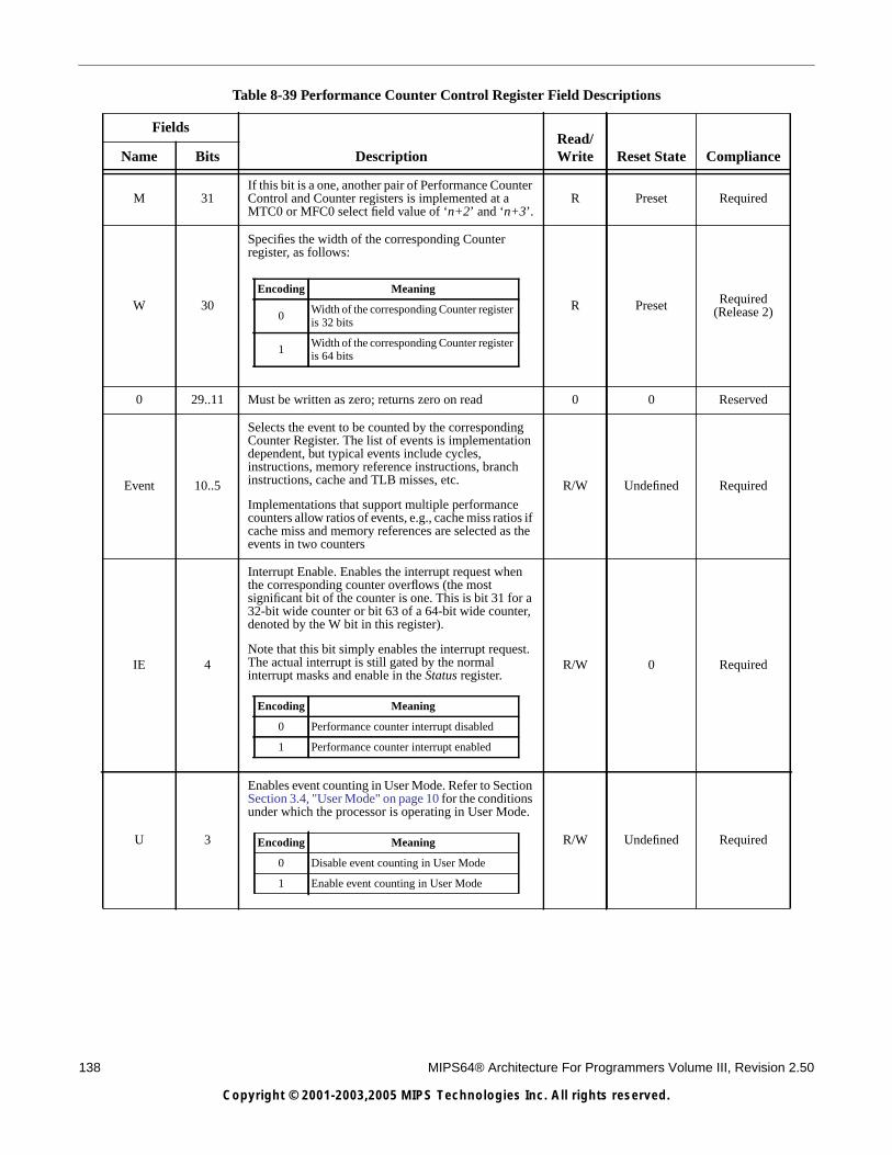
138 MIPS64® Architecture For Programmers Volume III, Revision 2.50
Copyright © 2001-2003,2005 MIPS Technologies Inc. All rights reserved.
Table 8-39 Performance Counter Control Register Field Descriptions
Fields
DescriptionRead/Write Reset State ComplianceName Bits
M 31If this bit is a one, another pair of Performance CounterControl and Counter registers is implemented at aMTC0 or MFC0 select field value of ‘n+2’ and ‘n+3’.
R Preset Required
W 30
Specifies the width of the corresponding Counterregister, as follows:
R Preset Required(Release 2)
0 29..11 Must be written as zero; returns zero on read 0 0 Reserved
Event 10..5
Selects the event to be counted by the correspondingCounter Register. The list of events is implementationdependent, but typical events include cycles,instructions, memory reference instructions, branchinstructions, cache and TLB misses, etc.
Implementations that support multiple performancecounters allow ratios of events, e.g., cache miss ratios ifcache miss and memory references are selected as theevents in two counters
R/W Undefined Required
IE 4
Interrupt Enable. Enables the interrupt request whenthe corresponding counter overflows (the mostsignificant bit of the counter is one. This is bit 31 for a32-bit wide counter or bit 63 of a 64-bit wide counter,denoted by the W bit in this register).
Note that this bit simply enables the interrupt request.The actual interrupt is still gated by the normalinterrupt masks and enable in the Status register.
R/W 0 Required
U 3
Enables event counting in User Mode. Refer to SectionSection 3.4, "User Mode" on page 10 for the conditionsunder which the processor is operating in User Mode.
R/W Undefined Required
Encoding Meaning
0Width of the corresponding Counter registeris 32 bits
1Width of the corresponding Counter registeris 64 bits
Encoding Meaning
0 Performance counter interrupt disabled
1 Performance counter interrupt enabled
Encoding Meaning
0 Disable event counting in User Mode
1 Enable event counting in User Mode
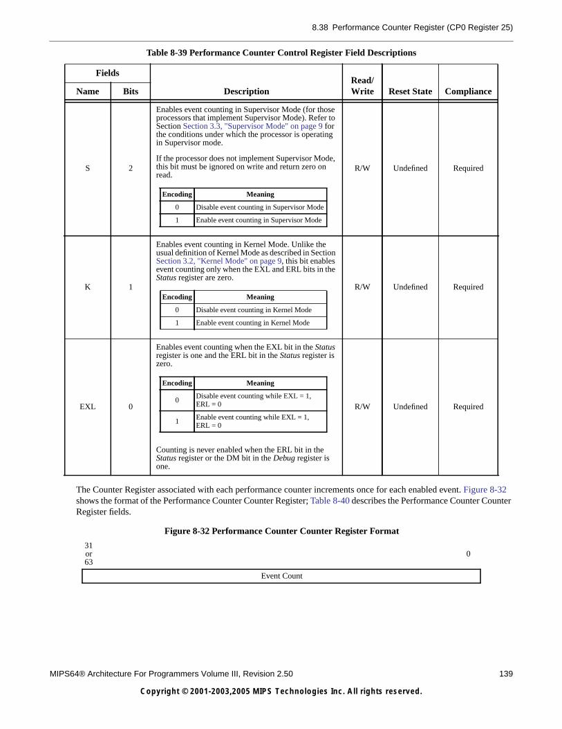
8.38 Performance Counter Register (CP0 Register 25)
MIPS64® Architecture For Programmers Volume III, Revision 2.50 139
Copyright © 2001-2003,2005 MIPS Technologies Inc. All rights reserved.
The Counter Register associated with each performance counter increments once for each enabled event. Figure 8-32shows the format of the Performance Counter Counter Register; Table 8-40 describes the Performance Counter CounterRegister fields.
S 2
Enables event counting in Supervisor Mode (for thoseprocessors that implement Supervisor Mode). Refer toSection Section 3.3, "Supervisor Mode" on page 9 forthe conditions under which the processor is operatingin Supervisor mode.
If the processor does not implement Supervisor Mode,this bit must be ignored on write and return zero onread.
R/W Undefined Required
K 1
Enables event counting in Kernel Mode. Unlike theusual definition of Kernel Mode as described in SectionSection 3.2, "Kernel Mode" on page 9, this bit enablesevent counting only when the EXL and ERL bits in theStatus register are zero.
R/W Undefined Required
EXL 0
Enables event counting when the EXL bit in the Statusregister is one and the ERL bit in the Status register iszero.
Counting is never enabled when the ERL bit in theStatus register or the DM bit in the Debug register isone.
R/W Undefined Required
Figure 8-32 Performance Counter Counter Register Format
31or63
0
Event Count
Table 8-39 Performance Counter Control Register Field Descriptions
Fields
DescriptionRead/Write Reset State ComplianceName Bits
Encoding Meaning
0 Disable event counting in Supervisor Mode
1 Enable event counting in Supervisor Mode
Encoding Meaning
0 Disable event counting in Kernel Mode
1 Enable event counting in Kernel Mode
Encoding Meaning
0Disable event counting while EXL = 1,ERL = 0
1Enable event counting while EXL = 1,ERL = 0

140 MIPS64® Architecture For Programmers Volume III, Revision 2.50
Copyright © 2001-2003,2005 MIPS Technologies Inc. All rights reserved.
Programming Note:
In Release 2 of the Architecture, the EHB instruction can be used to make interrupt state changes visible when the IEfield of the Control register or the Event Count Field of the Counter register are written. See Section 5.1.2.1, "Soft-ware Hazards and the Interrupt System" on page 40.
Table 8-40 Performance Counter Counter Register Field Descriptions
Fields
DescriptionRead/Write Reset State ComplianceName Bits
EventCount
31..0or
63..0
Increments once for each event that is enabled by thecorresponding Control Register. When the mostsignificant bit is one, a pending interrupt request isORed with those from other performance counters andindicated by the PCI bit in the Cause register.
The width of the counter is either 32 bits or 64 bitsdepending on the value of the W bit in thecorresponding Performance Counter Control Register.
R/W Undefined Required
8.39 ErrCtl Register (CP0 Register 26, Select 0)
MIPS64® Architecture For Programmers Volume III, Revision 2.50 141
Copyright © 2001-2003,2005 MIPS Technologies Inc. All rights reserved.
8.39 ErrCtl Register (CP0 Register 26, Select 0)
Compliance Level: Optional.
The ErrCtl register provides an implementation dependent diagnostic interface with the error detection mechanismsimplemented by the processor. This register has been used in previous implementations to read and write parity or ECCinformation to and from the primary or secondary cache data arrays in conjunction with specific encodings of the Cacheinstruction or other implementation-dependent method. The exact format of the ErrCtl register is implementationdependent and not specified by the architecture. Refer to the processor specification for the format of this register and adescription of the fields.
142 MIPS64® Architecture For Programmers Volume III, Revision 2.50
Copyright © 2001-2003,2005 MIPS Technologies Inc. All rights reserved.
8.40 CacheErr Register (CP0 Register 27, Select 0)
Compliance Level: Optional.
The CacheErr register provides an interface with the cache error detection logic that may be implemented by a processor.
The exact format of the CacheErr register is implementation dependent and not specified by the architecture. Refer tothe processor specification for the format of this register and a description of the fields.
8.41 TagLo Register (CP0 Register 28, Select 0, 2)
MIPS64® Architecture For Programmers Volume III, Revision 2.50 143
Copyright © 2001-2003,2005 MIPS Technologies Inc. All rights reserved.
8.41 TagLo Register (CP0 Register 28, Select 0, 2)
Compliance Level: Required if a cache is implemented; Optional otherwise.
The TagLo and TagHi registers are read/write registers that act as the interface to the cache tag array. The Index StoreTag and Index Load Tag operations of the CACHE instruction use the TagLo and TagHi registers as the source or sinkof tag information, respectively.
The exact format of the TagLo and TagHi registers is implementation dependent. Refer to the processor specificationfor the format of this register and a description of the fields.
However, software must be able to write zeros into the TagLo and TagHi registers and then use the Index Store Tagcache operation to initialize the cache tags to a valid state at powerup.
It is implementation dependent whether there is a single TagLo register that acts as the interface to all caches, or adedicated TagLo register for each cache. If multiple TagLo registers are implemented, they occupy the even select valuesfor this register encoding, with select 0 addressing the instruction cache and select 2 addressing the data cache. Whetherindividual TagLo registers are implemented or not for each cache, processors must accept a write of zero to select 0 andselect 2 of TagLo as part of the software process of initializing the cache tags at powerup.
144 MIPS64® Architecture For Programmers Volume III, Revision 2.50
Copyright © 2001-2003,2005 MIPS Technologies Inc. All rights reserved.
8.42 DataLo Register (CP0 Register 28, Select 1, 3)
Compliance Level: Optional.
The DataLo and DataHi registers are read-only registers that act as the interface to the cache data array and are intendedfor diagnostic operation only. The Index Load Tag operation of the CACHE instruction reads the corresponding datavalues into the DataLo and DataHi registers.
The exact format and operation of the DataLo and DataHi registers is implementation dependent. Refer to the processorspecification for the format of this register and a description of the fields.
It is implementation dependent whether there is a single DataLo register that acts as the interface to all caches, or adedicated DataLo register for each cache. If multiple DataLo registers are implemented, they occupy the odd selectvalues for this register encoding, with select 1 addressing the instruction cache and select 3 addressing the data cache.
8.43 TagHi Register (CP0 Register 29, Select 0, 2)
MIPS64® Architecture For Programmers Volume III, Revision 2.50 145
Copyright © 2001-2003,2005 MIPS Technologies Inc. All rights reserved.
8.43 TagHi Register (CP0 Register 29, Select 0, 2)
Compliance Level: Required if a cache is implemented; Optional otherwise.
The TagLo and TagHi registers are read/write registers that act as the interface to the cache tag array. The Index StoreTag and Index Load Tag operations of the CACHE instruction use the TagLo and TagHi registers as the source or sinkof tag information, respectively.
The exact format of the TagLo and TagHi registers is implementation dependent. Refer to the processor specificationfor the format of this register and a description of the fields. However, software must be able to write zeros into theTagLo and TagHi registers and the use the Index Store Tag cache operation to initialize the cache tags to a valid state atpowerup.
It is implementation dependent whether there is a single TagHi register that acts as the interface to all caches, or adedicated TagHi register for each cache. If multiple TagHi registers are implemented, they occupy the even select valuesfor this register encoding, with select 0 addressing the instruction cache and select 2 addressing the data cache. Whetherindividual TagHi registers are implemented or not for each cache, processors must accept a write of zero to select 0 andselect 2 of TagHi as part of the software process of initializing the cache tags at powerup.

146 MIPS64® Architecture For Programmers Volume III, Revision 2.50
Copyright © 2001-2003,2005 MIPS Technologies Inc. All rights reserved.
8.44 DataHi Register (CP0 Register 29, Select 1, 3)
Compliance Level: Optional.
The DataLo and DataHi registers are read-only registers that act as the interface to the cache data array and are intendedfor diagnostic operation only. The Index Load Tag operation of the CACHE instruction reads the corresponding datavalues into the DataLo and DataHi registers.
The exact format and operation of the DataLo and DataHi registers is implementation dependent. Refer to the processorspecification for the format of this register and a description of the fields.
8.45 ErrorEPC (CP0 Register 30, Select 0)
MIPS64® Architecture For Programmers Volume III, Revision 2.50 147
Copyright © 2001-2003,2005 MIPS Technologies Inc. All rights reserved.
8.45 ErrorEPC (CP0 Register 30, Select 0)
Compliance Level: Required.
The ErrorEPC register is a read-write register, similar to the EPC register, at which processing resumes after a Reset,Soft Reset, Nonmaskable Interrupt (NMI) or Cache Error exceptions (collectively referred to as error exceptions).Unlike the EPC register, there is no corresponding branch delay slot indication for the ErrorEPC register. All bits of theErrorEPC register are significant and must be writable.
When an error exception occurs, the processor writes the ErrorEPC register with:
• the virtual address of the instruction that was the direct cause of the exception, or
• the virtual address of the immediately preceding branch or jump instruction when the error causing instruction is in abranch delay slot.
The processor reads the ErrorEPC register as the result of execution of the ERET instruction.
Software may write the ErrorEPC register to change the processor resume address and read the ErrorEPC register todetermine at what address the processor will resume
Figure 8-33 shows the format of the ErrorEPC register; Table 8-41 describes the ErrorEPC register fields.
8.45.1 Special Handling of the ErrorEPC Register in Processors That Implement the MIPS16e ASE
In processors that implement the MIPS16e ASE, the ErrorEPC register requires special handling.
When the processor writes the ErrorEPC register, it combines the address at which processing resumes with the valueof the ISA Mode register:
ErrorEPC ← resumePC63..1 || ISAMode0
“resumePC” is the address at which processing resumes, as described above.
When the processor reads the ErrorEPC register, it distributes the bits to the PC and ISAMode registers:
PC ← ErrorEPC63..1 || 0ISAMode ← ErrorEPC0
Software reads of the ErrorEPC register simply return to a GPR the last value written with no interpretation. Softwarewrites to the ErrorEPC register store a new value which is interpreted by the processor as described above.
Figure 8-33 ErrorEPC Register Format
63 0
ErrorEPC
Table 8-41 ErrorEPC Register Field Descriptions
Fields
DescriptionRead/Write Reset State ComplianceName Bits
ErrorEPC 63..0 Error Exception Program Counter R/W Undefined Required
148 MIPS64® Architecture For Programmers Volume III, Revision 2.50
Copyright © 2001-2003,2005 MIPS Technologies Inc. All rights reserved.
8.46 DESAVE Register (CP0 Register 31)
Compliance Level: Optional.
The DESAVE register is part of the EJTAG specification. Refer to that specification for the format and description ofthis register.
MIPS64® Architecture For Programmers Volume III, Revision 2.50 149
Copyright © 2001-2003,2005 MIPS Technologies Inc. All rights reserved.
Appendix A
Alternative MMU Organizations
The main body of this specification describes the TLB-based MMU organization. This appendix describes otherpotential MMU organizations.
A.1 Fixed Mapping MMU
As an alternative to the full TLB-based MMU, the MIPS64 Architecture supports a lightweight memory managementmechanism with fixed virtual-to-physical address translation, and no memory protection beyond what is provided by theaddress error checks required of all MMUs. This may be useful for those applications which do not require thecapabilities of a full TLB-based MMU. It is not anticipated that MIPS64 processors that implement a fixed-mappingMMU will require a 64-bit address capability. As a result, the description below is given assuming a 32-bit address.
A.1.1 Fixed Address Translation
Address translation using the Fixed Mapping MMU is done as follows:
• Kseg0 and Kseg1 addresses are translated in an identical manner to the TLB-based MMU: they both map to the low512MB of physical memory.
• Useg/Suseg/Kuseg addresses are mapped by adding 1GB to the virtual address when the ERL bit is zero in the Statusregister, and are mapped using an identity mapping when the ERL bit is one in the Status register.
• Sseg/Ksseg/Kseg2/Kseg3 addresses are mapped using an identity mapping.
Supervisor Mode is not supported with a Fixed Mapping MMU.
Table 8-42 lists all mappings from virtual to physical addresses. Note that address error checking is still done before thetranslation process. Therefore, an attempt to reference kseg0 from User Mode still results in an address error exception,just as it does with a TLB-based MMU.
Table 8-42 Physical Address Generation from Virtual Addresses
SegmentName Virtual Address
Generates Physical Address
StatusERL = 0 StatusERL = 1
useg
suseg
kuseg
0x0000 0000
through
0x7FFF FFFF
0x4000 0000
through
0xBFFF FFFF
0x0000 0000
through
0x7FFF FFFF
kseg0
0x8000 0000
through
0x9FFF FFFF
0x0000 0000
through
0x1FFF FFFF
kseg1
0xA000 0000
through
0xBFFF FFFF
0x0000 0000
through
0x0x1FFF FFFF
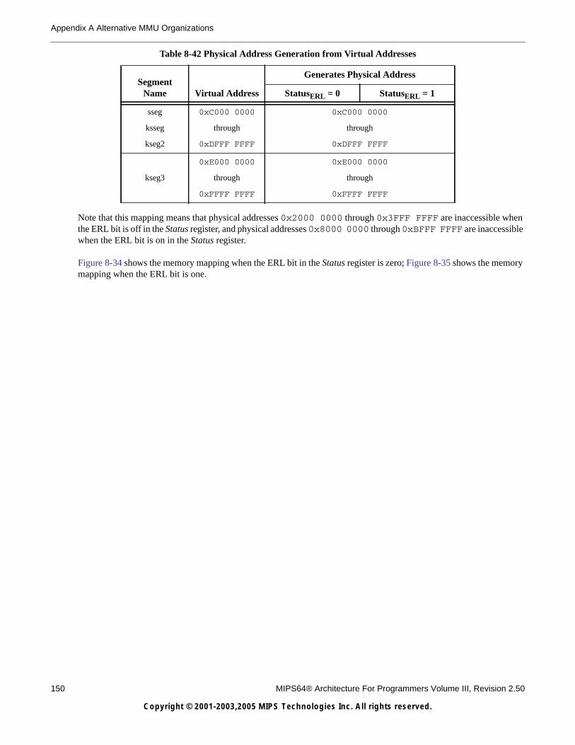
150 MIPS64® Architecture For Programmers Volume III, Revision 2.50
Copyright © 2001-2003,2005 MIPS Technologies Inc. All rights reserved.
Appendix A Alternative MMU Organizations
Note that this mapping means that physical addresses 0x2000 0000 through 0x3FFF FFFF are inaccessible whenthe ERL bit is off in the Status register, and physical addresses 0x8000 0000 through 0xBFFF FFFF are inaccessiblewhen the ERL bit is on in the Status register.
Figure 8-34 shows the memory mapping when the ERL bit in the Status register is zero; Figure 8-35 shows the memorymapping when the ERL bit is one.
sseg
ksseg
kseg2
0xC000 0000
through
0xDFFF FFFF
0xC000 0000
through
0xDFFF FFFF
kseg3
0xE000 0000
through
0xFFFF FFFF
0xE000 0000
through
0xFFFF FFFF
Table 8-42 Physical Address Generation from Virtual Addresses
SegmentName Virtual Address
Generates Physical Address
StatusERL = 0 StatusERL = 1
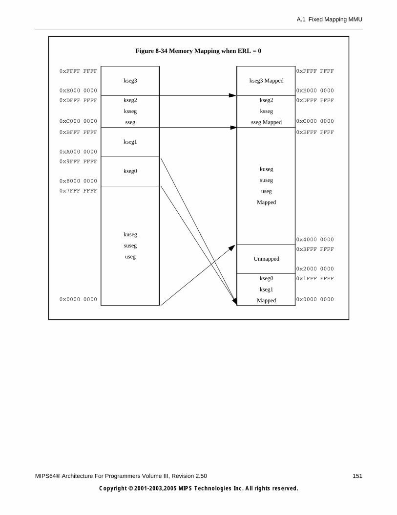
A.1 Fixed Mapping MMU
MIPS64® Architecture For Programmers Volume III, Revision 2.50 151
Copyright © 2001-2003,2005 MIPS Technologies Inc. All rights reserved.
Figure 8-34 Memory Mapping when ERL = 0
0xFFFF FFFF
kseg3 kseg3 Mapped
0xFFFF FFFF
0xE000 0000 0xE000 0000
0xDFFF FFFF kseg2
ksseg
sseg
kseg2
ksseg
sseg Mapped
0xDFFF FFFF
0xC000 0000 0xC000 0000
0xBFFF FFFF
kseg1
kuseg
suseg
useg
Mapped
0xBFFF FFFF
0xA000 0000
0x9FFF FFFF
kseg0
0x8000 0000
0x7FFF FFFF
kuseg
suseg
useg
0x4000 0000
Unmapped
0x3FFF FFFF
0x2000 0000
kseg0
kseg1
Mapped
0x1FFF FFFF
0x0000 0000 0x0000 0000
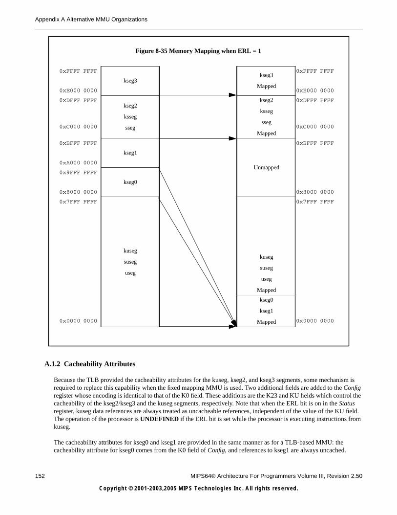
152 MIPS64® Architecture For Programmers Volume III, Revision 2.50
Copyright © 2001-2003,2005 MIPS Technologies Inc. All rights reserved.
Appendix A Alternative MMU Organizations
A.1.2 Cacheability Attributes
Because the TLB provided the cacheability attributes for the kuseg, kseg2, and kseg3 segments, some mechanism isrequired to replace this capability when the fixed mapping MMU is used. Two additional fields are added to the Configregister whose encoding is identical to that of the K0 field. These additions are the K23 and KU fields which control thecacheability of the kseg2/kseg3 and the kuseg segments, respectively. Note that when the ERL bit is on in the Statusregister, kuseg data references are always treated as uncacheable references, independent of the value of the KU field.The operation of the processor is UNDEFINED if the ERL bit is set while the processor is executing instructions fromkuseg.
The cacheability attributes for kseg0 and kseg1 are provided in the same manner as for a TLB-based MMU: thecacheability attribute for kseg0 comes from the K0 field of Config, and references to kseg1 are always uncached.
Figure 8-35 Memory Mapping when ERL = 1
0xFFFF FFFF
kseg3kseg3
Mapped
0xFFFF FFFF
0xE000 0000 0xE000 0000
0xDFFF FFFFkseg2
ksseg
sseg
kseg2
ksseg
sseg
Mapped
0xDFFF FFFF
0xC000 0000 0xC000 0000
0xBFFF FFFF
kseg1
Unmapped
0xBFFF FFFF
0xA000 0000
0x9FFF FFFF
kseg0
0x8000 0000 0x8000 0000
0x7FFF FFFF
kuseg
suseg
useg
kuseg
suseg
useg
Mapped
0x7FFF FFFF
kseg0
kseg1
Mapped0x0000 0000 0x0000 0000
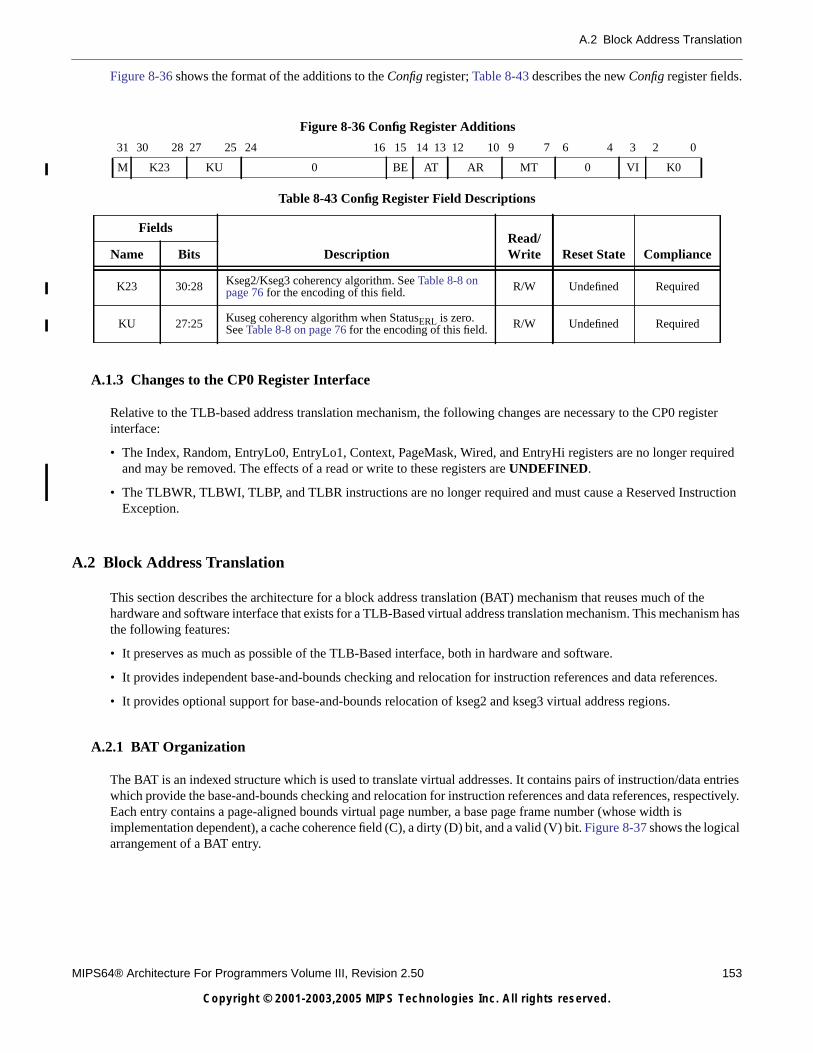
A.2 Block Address Translation
MIPS64® Architecture For Programmers Volume III, Revision 2.50 153
Copyright © 2001-2003,2005 MIPS Technologies Inc. All rights reserved.
Figure 8-36 shows the format of the additions to the Config register; Table 8-43 describes the new Config register fields.
A.1.3 Changes to the CP0 Register Interface
Relative to the TLB-based address translation mechanism, the following changes are necessary to the CP0 registerinterface:
• The Index, Random, EntryLo0, EntryLo1, Context, PageMask, Wired, and EntryHi registers are no longer requiredand may be removed. The effects of a read or write to these registers are UNDEFINED.
• The TLBWR, TLBWI, TLBP, and TLBR instructions are no longer required and must cause a Reserved InstructionException.
A.2 Block Address Translation
This section describes the architecture for a block address translation (BAT) mechanism that reuses much of thehardware and software interface that exists for a TLB-Based virtual address translation mechanism. This mechanism hasthe following features:
• It preserves as much as possible of the TLB-Based interface, both in hardware and software.
• It provides independent base-and-bounds checking and relocation for instruction references and data references.
• It provides optional support for base-and-bounds relocation of kseg2 and kseg3 virtual address regions.
A.2.1 BAT Organization
The BAT is an indexed structure which is used to translate virtual addresses. It contains pairs of instruction/data entrieswhich provide the base-and-bounds checking and relocation for instruction references and data references, respectively.Each entry contains a page-aligned bounds virtual page number, a base page frame number (whose width isimplementation dependent), a cache coherence field (C), a dirty (D) bit, and a valid (V) bit. Figure 8-37 shows the logicalarrangement of a BAT entry.
Figure 8-36 Config Register Additions
31 30 28 27 25 24 16 15 14 13 12 10 9 7 6 4 3 2 0
M K23 KU 0 BE AT AR MT 0 VI K0
Table 8-43 Config Register Field Descriptions
Fields
DescriptionRead/Write Reset State ComplianceName Bits
K23 30:28 Kseg2/Kseg3 coherency algorithm. See Table 8-8 onpage 76 for the encoding of this field. R/W Undefined Required
KU 27:25 Kuseg coherency algorithm when StatusERL is zero.See Table 8-8 on page 76 for the encoding of this field. R/W Undefined Required
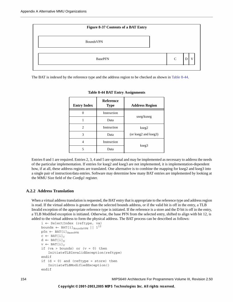
154 MIPS64® Architecture For Programmers Volume III, Revision 2.50
Copyright © 2001-2003,2005 MIPS Technologies Inc. All rights reserved.
Appendix A Alternative MMU Organizations
The BAT is indexed by the reference type and the address region to be checked as shown in Table 8-44.
Entries 0 and 1 are required. Entries 2, 3, 4 and 5 are optional and may be implemented as necessary to address the needsof the particular implementation. If entries for kseg2 and kseg3 are not implemented, it is implementation-dependenthow, if at all, these address regions are translated. One alternative is to combine the mapping for kseg2 and kseg3 intoa single pair of instruction/data entries. Software may determine how many BAT entries are implemented by looking atthe MMU Size field of the Config1 register.
A.2.2 Address Translation
When a virtual address translation is requested, the BAT entry that is appropriate to the reference type and address regionis read. If the virtual address is greater than the selected bounds address, or if the valid bit is off in the entry, a TLBInvalid exception of the appropriate reference type is initiated. If the reference is a store and the D bit is off in the entry,a TLB Modified exception is initiated. Otherwise, the base PFN from the selected entry, shifted to align with bit 12, isadded to the virtual address to form the physical address. The BAT process can be described as follows:
i ← SelectIndex (reftype, va)bounds ← BAT[i]BoundsVPN || 112
pfn ← BAT[i]BasePFNc ← BAT[i]Cd ← BAT[i]Dv ← BAT[i]Vif (va > bounds) or (v = 0) then
InitiateTLBInvalidException(reftype)endifif (d = 0) and (reftype = store) then
InitiateTLBModifiedException()endif
Figure 8-37 Contents of a BAT Entry
BoundsVPN
BasePFN C D V
Table 8-44 BAT Entry Assignments
Entry IndexReference
Type Address Region
0 Instructionuseg/kuseg
1 Data
2 Instruction kseg2
(or kseg2 and kseg3)3 Data
4 Instructionkseg3
5 Data
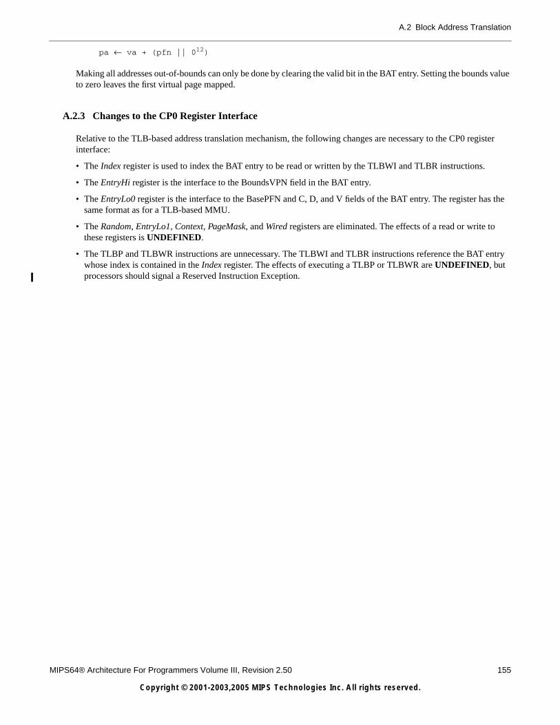
A.2 Block Address Translation
MIPS64® Architecture For Programmers Volume III, Revision 2.50 155
Copyright © 2001-2003,2005 MIPS Technologies Inc. All rights reserved.
pa ← va + (pfn || 012)
Making all addresses out-of-bounds can only be done by clearing the valid bit in the BAT entry. Setting the bounds valueto zero leaves the first virtual page mapped.
A.2.3 Changes to the CP0 Register Interface
Relative to the TLB-based address translation mechanism, the following changes are necessary to the CP0 registerinterface:
• The Index register is used to index the BAT entry to be read or written by the TLBWI and TLBR instructions.
• The EntryHi register is the interface to the BoundsVPN field in the BAT entry.
• The EntryLo0 register is the interface to the BasePFN and C, D, and V fields of the BAT entry. The register has thesame format as for a TLB-based MMU.
• The Random, EntryLo1, Context, PageMask, and Wired registers are eliminated. The effects of a read or write tothese registers is UNDEFINED.
• The TLBP and TLBWR instructions are unnecessary. The TLBWI and TLBR instructions reference the BAT entrywhose index is contained in the Index register. The effects of executing a TLBP or TLBWR are UNDEFINED, butprocessors should signal a Reserved Instruction Exception.
156 MIPS64® Architecture For Programmers Volume III, Revision 2.50
Copyright © 2001-2003,2005 MIPS Technologies Inc. All rights reserved.
Appendix A Alternative MMU Organizations

MIPS64® Architecture For Programmers Volume III, Revision 2.50 157
Copyright © 2001-2003,2005 MIPS Technologies Inc. All rights reserved.
Appendix B
Revision History
In the left hand page margins of this document you may find vertical change bars to note the location of significantchanges to this document since its last release. Significant changes are defined as those which you should take note ofas you use the MIPS IP. Changes to correct grammar, spelling errors or similar may or may not be noted with changebars. Change bars will be removed for changes which are more than one revision old.
Please note: Limitations on the authoring tools make it difficult to place change bars on changes to figures. Change barson figure titles are used to denote a potential change in the figure itself.
Revision Date Description
0.92 January 20, 2001 Internal review copy of reorganized and updated architecture documentation.
0.95 March 12, 2001 Clean up document for external review release
1.00 August 29, 2002
Update based on review feedback:
• Change ProbEn to ProbeTrap in the EJTAG Debug entry vector locationdiscussion.
• Add cache error and EJTAG Debug exceptions to the list of exceptions thatdo not go through the general exception processing mechanism.
• Fix incorrect branch offset adjustment in general exception processingpseudo code to deal with extended MIPS16e instructions.
• Add ConfigVI to denote an instruction cache with both virtual indexing andvirtual tags.
• Correct XContext register description to note that both BadVPN2 and Rfields are UNPREDICTABLE after an address error exception.
• Note that Supervisor Mode is not supported with a Fixed Mapping MMU.
• Define TagLo bits 4..3 as implementation dependent.
• Describe the intended usage model differences between Reset and SoftReset Exceptions.
• Correct the minimum number of TLB entries to be 3, not 2, and show anexample of the need for 3.
• Modify the description of PageMask and the TLB lookup process toacknowledge the fact that not all implementations may support all pagesizes.
1.90 September 1, 2002
Update the specification with the changes introduced in Release 2 of theArchitecture. Changes in this revision include:
• The following new Coprocessor 0 registers were added: EBase, HWREna,IntCtl, PageGrain, SRSCtl, SRSMap.
• The following Coprocessor 0 registers were modified: Cause, Config,Config2, Config3, EntryHi, EntryLo0, EntryLo1, PageMask, PerfCnt,Status, WatchHi, WatchLo.
• The descriptions of Virtual memory, exceptions, and hazards have beenupdated to reflect the changes in Release 2.
• A chapter on GPR shadow regsiters has been added.
• The chapter on CP0 hazards has been completely rewriten to reflect theRelease 2 changes.
158 MIPS64® Architecture For Programmers Volume III, Revision 2.50
Copyright © 2001-2003,2005 MIPS Technologies Inc. All rights reserved.
Appendix B Revision History
2.00 June 9, 2003
Complete the update to include Release 2 changes. These include:
• Make bits 12..11 of the PageMask register power up zero and be gated by1K page enable. This eliminates the problem of having these bits set to 0b11on a Release 2 chip in which kernel software has not enabled 1K pagesupport.
• Correct the address of the cache error vector when the BEV bit is 1. Itshould be 0xBFC0.0300,. not 0xBFC0.0200.
• Correct the introduction to shadow registers to note that the SRSCtl registeris not updated at the end of an exception in which StatusBEV = 1.
• Clarify that a MIPS16e PC-relative load reference is a data reference for thepurposes of the Watch registers.
• Add note about a hardware interrupt being deasserted between the time thatthe processor detects the interrupt request and the time that the softwareinterrupt handler runs. Software must be prepared for this case and simplydismiss the interrupt via an ERET.
• Add restriction that software must set EBase15..12 to zero in all bit positionsless than or equal to the most significant bit in the vector offset. This is onlyrequired in certain combinations of vector number and vector spacing whenusing VI or EIC Interrupt modes.
• Add suggested software TLB init routine which reduced the probability oftriggering a machine check.
Revision Date Description
MIPS64® Architecture For Programmers Volume III, Revision 2.50 159
Copyright © 2001-2003,2005 MIPS Technologies Inc. All rights reserved.
2.50 July 1, 2005
Changes in this revision:
• Correct the encoding table description for the CausePCI bit to indicate thatthe bit controlls the performance counter, not the timer interrupt.
• Correct the figure Interrupt Generation for External Interrupt ControllerInterrupt Mode to show CauseIP1..0 going to the EIC, rather than StatusIP1..0
• Update all files to FrameMaker 7.1.
• Update reset exception list to reflect missing Release 2 reset requirements.
• Define bits 31..30 in the HWREna register as access enables for theimplementation-dependent hardware registers 31 and 30.
• Add definition for Coprocessor 0 Enable to Operating Modes chapter.
• Add K23 and KU fields to main Config register definition as a pointer to theFixed Mapping MMU appendix.
• Add specific note about the need to implement all shadow sets between 0and HSS - no holes are allowed.
• Change the hazard from a software write to the SRSCtlPSS field and aRDPGPR and WRPGPR and instruction hazard vs. an execution hazard.
• Correct the pseudo-code in the cache error exception description to reflectthe Release 2 change that introduced EBase.
• Document that EHB clears instruction state change hazards for writes tointerrupt-related fields in the Status, Cause, Compare, and PerfCnt registers.
• Note that implementation-dependent bits in the Status and Config registersshould be defined in such a way that standard boot software will run, andthat software which preserves the value of the field when writing theregisters will also run correctly.
• With Release 2 of the Architecture the FR bit in the Status register should bea R/W bit, not a R bit.
• Improve the organization of the CP0 hazards table, and document thatDERET, ERET, and exceptions and interrupts clear all hazards before theinstruction fetch at the target instruction.
• Add list of MIPS® MT CP0 registers and MIPS MT and MIPS® DSPpresent bits in the Config3 register.
Revision Date Description