mips single and multi cycle data paths mite 2
DESCRIPTION
MIPS Single and Multi Cycle Data Paths Mite 2. Ellen Spertus MCS 111 October 31, 2002. Today. MIPS: single-cycle datapath Review Definitions Timing Instructions to control bits MIPS: multi-cycle datapth Lab: Mite 2. Big picture. - PowerPoint PPT PresentationTRANSCRIPT
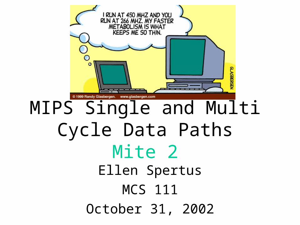
MIPS Single and Multi Cycle Data Paths
Mite 2Ellen Spertus
MCS 111
October 31, 2002

2
3
Today
• MIPS: single-cycle datapath– Review– Definitions– Timing– Instructions to control bits
• MIPS: multi-cycle datapth• Lab: Mite 2
4
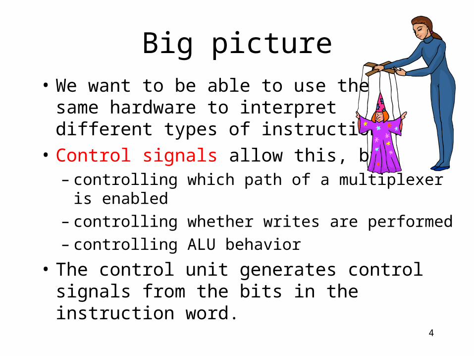
Big picture
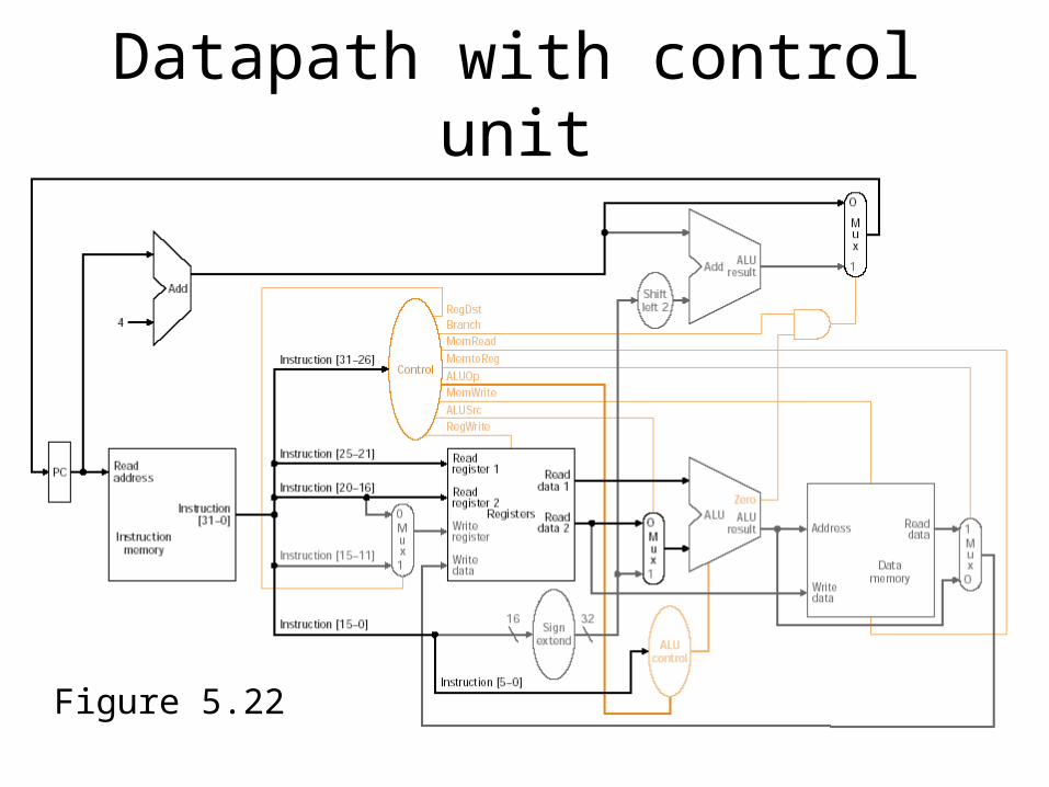
• We want to be able to use the same hardware to interpret different types of instructions.
• Control signals allow this, by– controlling which path of a multiplexer is
enabled– controlling whether writes are performed– controlling ALU behavior
• The control unit generates control signals from the bits in the instruction word.
5
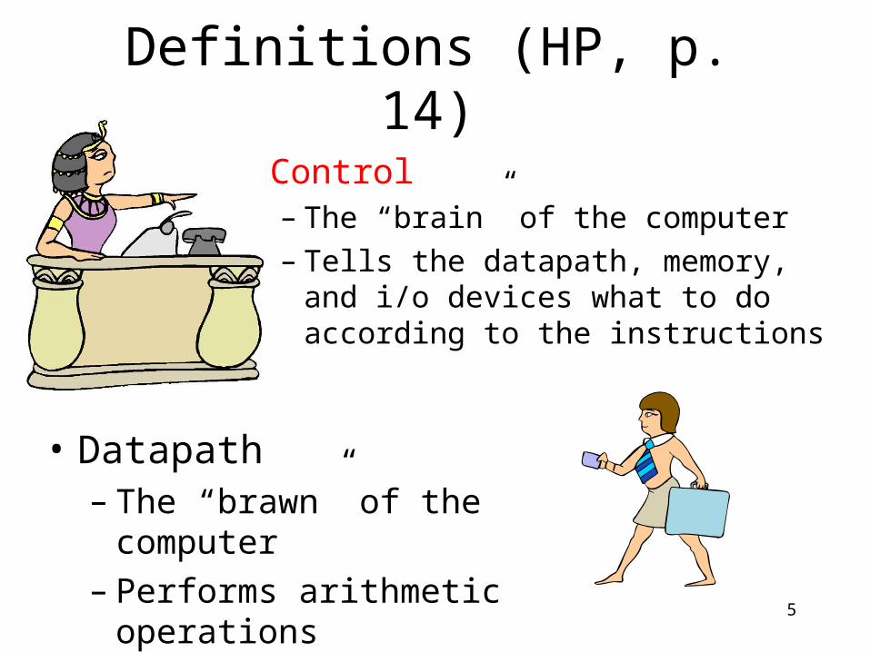
Definitions (HP, p. 14)
• Control– The “brain” of the computer– Tells the datapath, memory, and
i/o devices what to do according to the instructions
• Datapath– The “brawn” of the computer– Performs arithmetic operations
6
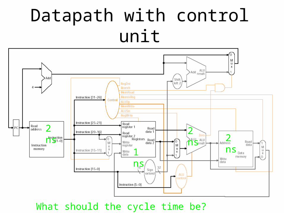
Datapath with control unit
Figure 5.22
7
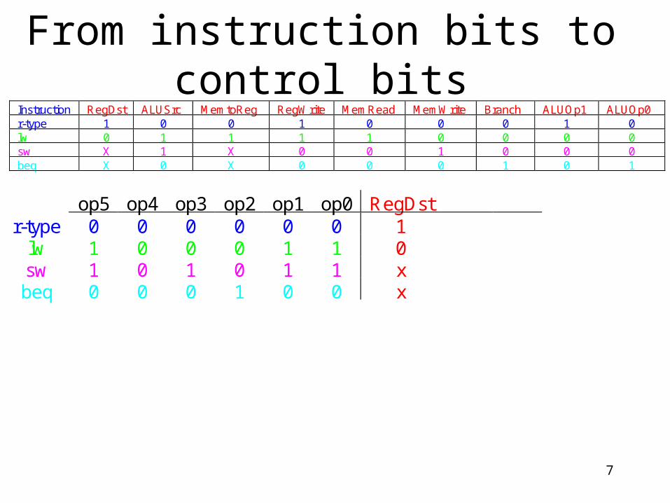
From instruction bits to control bitsInstruction RegDst ALUSrc MemtoReg RegWrite MemRead MemWrite Branch ALUOp1 ALUOp0 r-type 1 0 0 1 0 0 0 1 0 lw 0 1 1 1 1 0 0 0 0 sw X 1 X 0 0 1 0 0 0 beq X 0 X 0 0 0 1 0 1
op5 op4 op3 op2 op1 op0 RegDst r-type 0 0 0 0 0 0 1
lw 1 0 0 0 1 1 0 sw 1 0 1 0 1 1 x beq 0 0 0 1 0 0 x
8
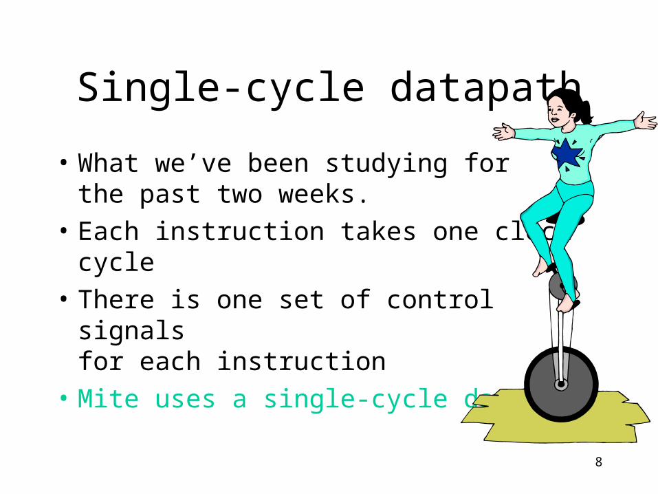
Single-cycle datapath
• What we’ve been studying forthe past two weeks.
• Each instruction takes one clock cycle
• There is one set of control signalsfor each instruction
• Mite uses a single-cycle datapath
9
Datapath with control unit
What should the cycle time be?
2 ns
1 ns
2 ns2 ns
10
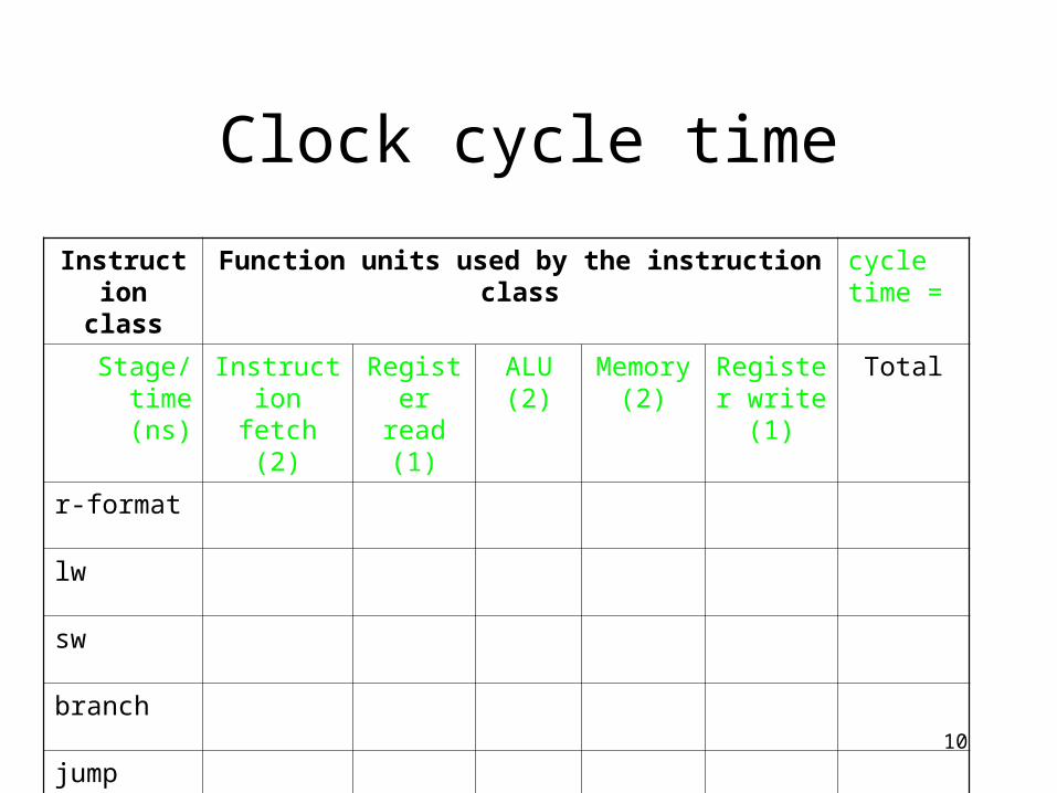
Clock cycle time
Instruction class
Function units used by the instruction class cycle time =
Stage/time (ns)
Instruction fetch (2)
Register read (1)
ALU (2)
Memory (2)
Register write (1)
Total
r-format
lw
sw
branch
jump
11
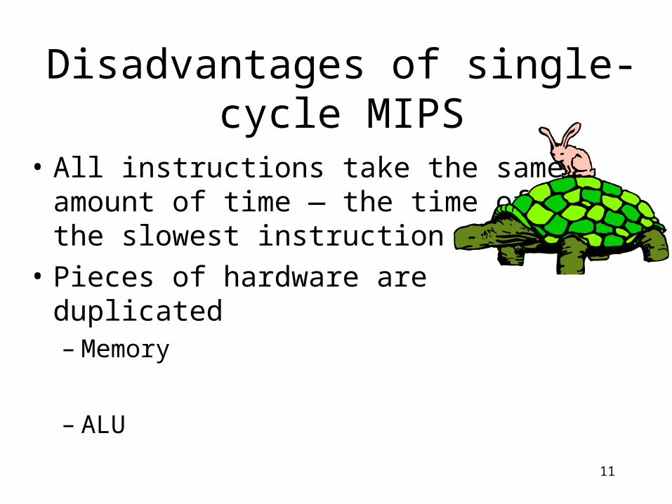
Disadvantages of single-cycle MIPS
• All instructions take the same amount of time — the time of the slowest instruction
• Pieces of hardware are duplicated– Memory
– ALU
12
Multicycle implementation
• Instructions take different amounts of time, depending on the number of stages they require
• Hardware can be reused– ALU– Memory
• Disadvantage: More complex control
13
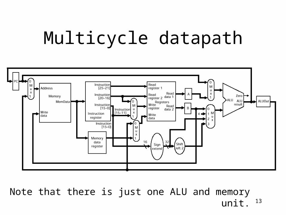
Multicycle datapath
Note that there is just one ALU and memory unit.
14
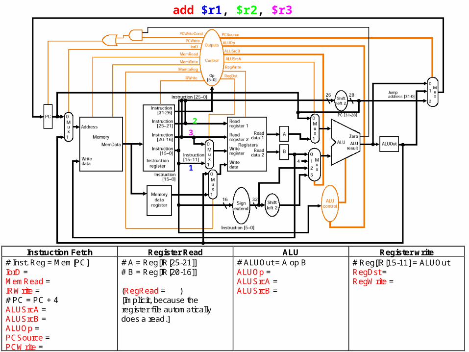
add $r1, $r2, $r3
1
2
3
Instruction Fetch Register Read ALU Register write # Inst. Reg = Mem[PC] IorD = MemRead = IRWrite = # PC = PC + 4 ALUSrcA = ALUSrcB = ALUOp = PCSource = PCWrite =
# A = Reg[IR[25-21]] # B = Reg[IR[20-16]] (RegRead = ) [Implicit, because the register file automatically does a read.]
# ALUOut = A op B ALUOp = ALUSrcA = ALUSrcB =
# Reg[IR[15-11] = ALUOut RegDst = RegWrite =
15
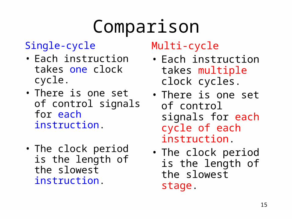
ComparisonSingle-cycle• Each instruction
takes one clock cycle.
• There is one set of control signalsfor each instruction.
• The clock period is the length of the slowest instruction.
Multi-cycle• Each instruction
takes multiple clock cycles.
• There is one set of control signals for each cycle of each instruction.
• The clock period is the length of the slowest stage.
16
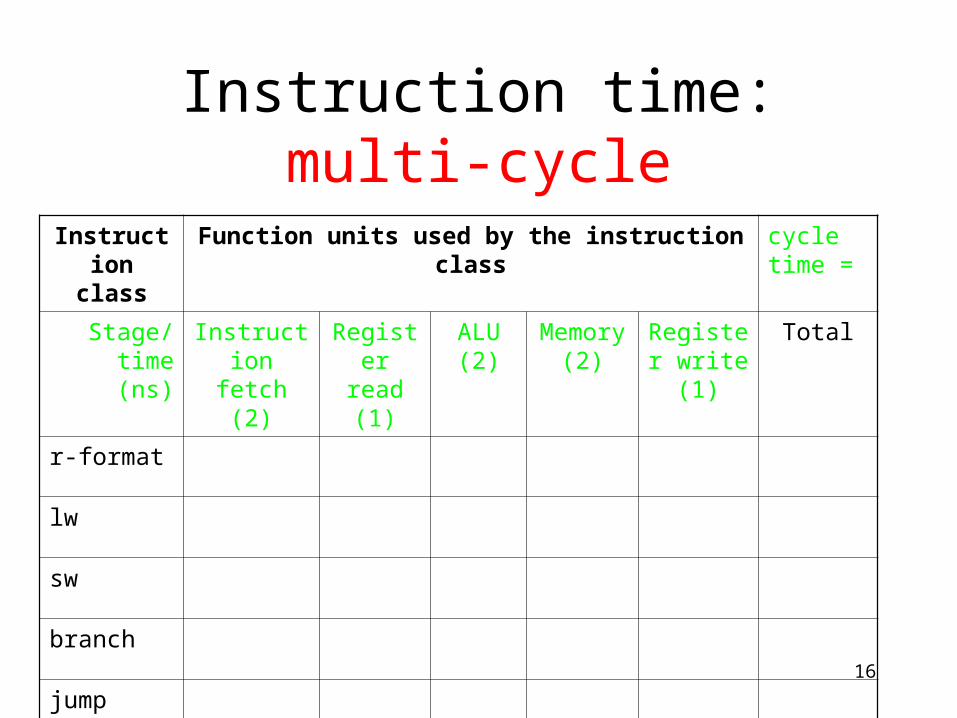
Instruction time: multi-cycle
Instruction class
Function units used by the instruction class cycle time =
Stage/time (ns)
Instruction fetch (2)
Register read (1)
ALU (2)
Memory (2)
Register write (1)
Total
r-format
lw
sw
branch
jump
17
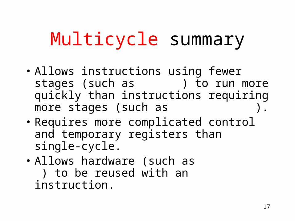
Multicycle summary
• Allows instructions using fewer stages (such as ) to run more quickly than instructions requiring more stages (such as ).
• Requires more complicated control and temporary registers than single-cycle.
• Allows hardware (such as ) to be reused with an instruction.
18
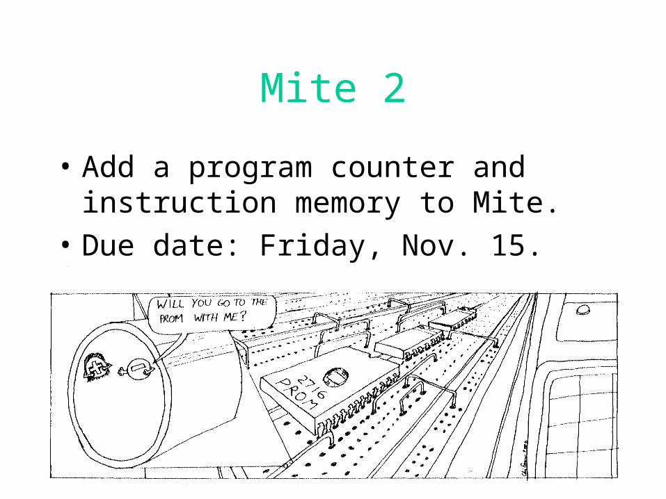
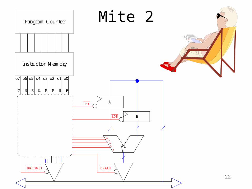
Mite 2
• Add a program counter and instruction memory to Mite.
• Due date: Friday, Nov. 15.
19
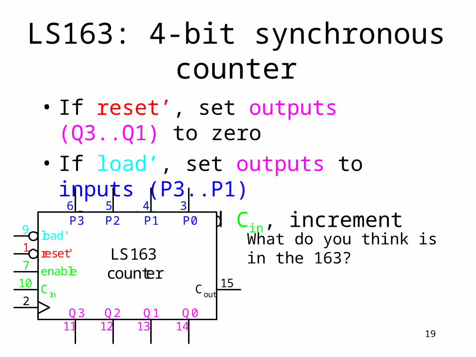
LS163: 4-bit synchronous counter
• If reset’, set outputs (Q3..Q1) to zero
• If load’, set outputs to inputs (P3..P1)
• If enable and Cin, increment outputs
enable
Cin
load'
reset'
P3 P0P2 P1
Q3 Q0Q2 Q1
Cout
1
2
7
6 5 4 3
9
10
1411 12 13
15
LS163counter
What do you think is in the 163?
20
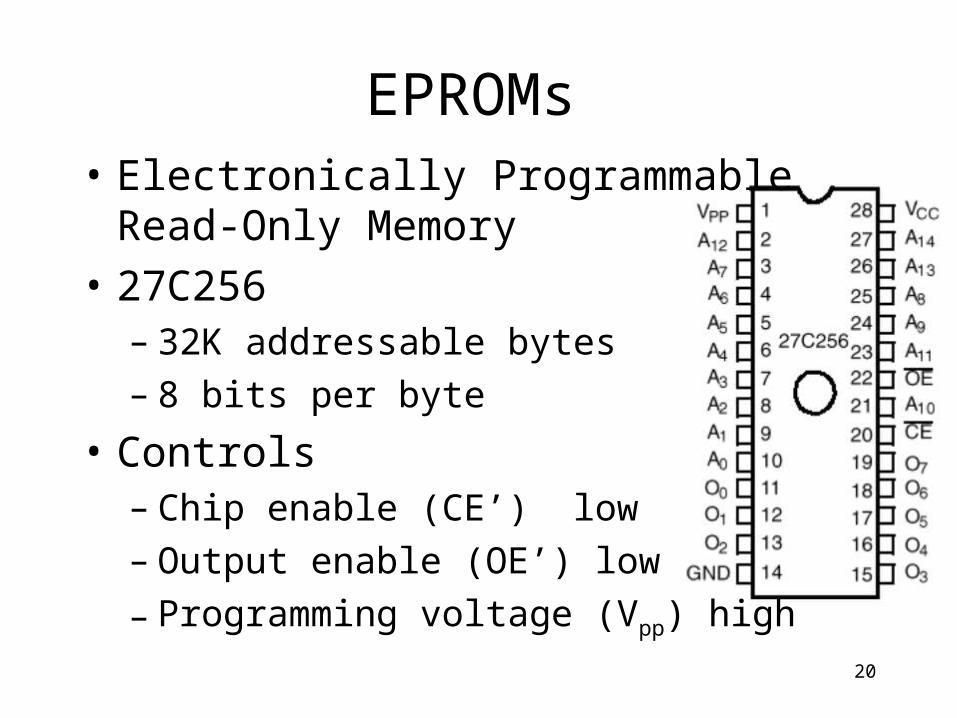
EPROMs• Electronically Programmable
Read-Only Memory
• 27C256– 32K addressable bytes– 8 bits per byte
• Controls– Chip enable (CE’) low– Output enable (OE’) low
– Programming voltage (Vpp) high
21
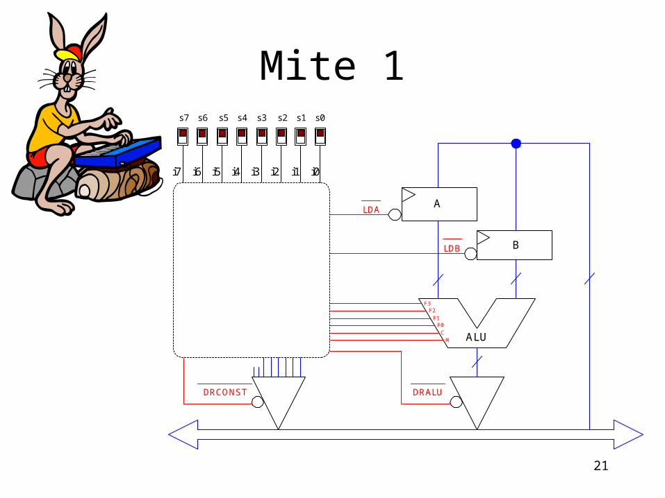
Mite 1
A
B
LDA
LDB
ALU
F3F2
F1F0
CM
DRALUDRCONST
i7 i4i6 i5 i3 i2 i1 i0
s0s4 s3 s2 s1s5s7 s6
22
Mite 2
A
B
LDA
LDB
ALU
F3 F
2 F1 F
0C
M
DRALUDRCONST
i7 i4i6 i5 i3 i2 i1 i0
o7 o4o6 o5 o3 o2 o1 o0
Instruction Memory
Program Counter
23
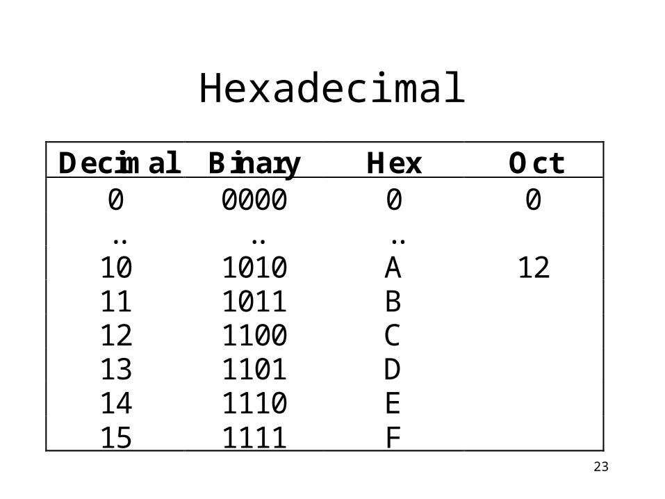
Hexadecimal
Decimal Binary Hex Oct 0 0000 0 0 .. .. ..
10 1010 A 12 11 1011 B 12 1100 C 13 1101 D 14 1110 E 15 1111 F
24
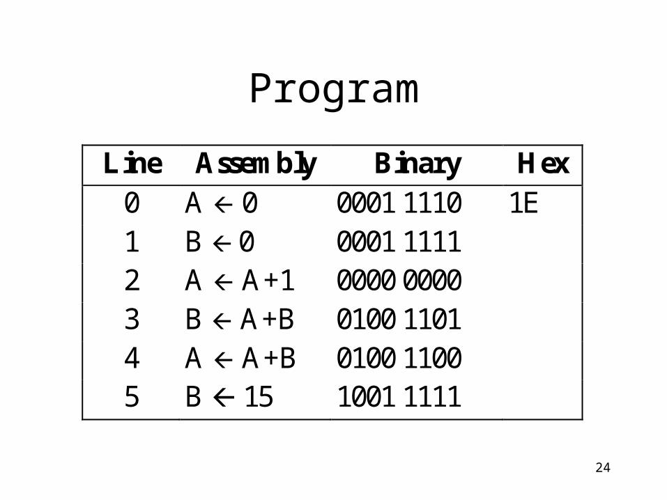
Program
Line Assembly Binary Hex 0 A 0 0001 1110 1E 1 B 0 0001 1111 2 A A+1 0000 0000 3 B A+B 0100 1101 4 A A+B 0100 1100 5 B 15 1001 1111