mips® architecture for programmers vol. iii: mips32 ... · document number: md00090 revision 6.02...
TRANSCRIPT
Document Number: MD00090Revision 6.02July 10, 2015
MIPS® Architecture For Programmers Vol. III: MIPS32® / microMIPS32™ Privileged Resource Architecture

2 MIPS® Architecture For Programmers Vol. III: MIPS32® / microMIPS32™ Privileged Resource Architecture, Rev. 6.02
Template: nB1.03, Built with tags: 2B ARCH MIPS32
Public. This publication contains proprietary information which is subject to change without notice and is supplied ‘as is’, without any warranty of any kind.
MIPS® Architecture For Programmers Vol. III: MIPS32® / microMIPS32™ Privileged Resource Architecture, Rev. 6.02 3
Contents
Chapter 1: About This Book ................................................................................................................ 131.1: Typographical Conventions ....................................................................................................................... 14
1.1.1: Italic Text.......................................................................................................................................... 141.1.2: Bold Text .......................................................................................................................................... 141.1.3: Courier Text ..................................................................................................................................... 14
1.2: UNPREDICTABLE and UNDEFINED ....................................................................................................... 141.2.1: UNPREDICTABLE........................................................................................................................... 141.2.2: UNDEFINED .................................................................................................................................... 151.2.3: UNSTABLE ...................................................................................................................................... 15
1.3: Special Symbols in Pseudocode Notation................................................................................................. 151.4: For More Information ................................................................................................................................. 18
Chapter 2: The MIPS32 and microMIPS32 Privileged Resource Architecture ................................ 192.1: Introduction................................................................................................................................................ 192.2: The MIPS Coprocessor Model .................................................................................................................. 19
2.2.1: CP0 - The System Coprocessor ...................................................................................................... 192.2.2: CP0 Registers .................................................................................................................................. 19
Chapter 3: MIPS32 and microMIPS32 Operating Modes................................................................... 213.1: Debug Mode ............................................................................................................................................. 213.2: Kernel Mode .............................................................................................................................................. 213.3: Supervisor Mode ....................................................................................................................................... 213.4: User Mode ................................................................................................................................................. 223.5: Other Modes.............................................................................................................................................. 22
3.5.1: 64-bit Floating-Point Operations Enable .......................................................................................... 223.5.2: 64-bit FPR Enable............................................................................................................................ 223.5.3: Coprocessor 0 Enable...................................................................................................................... 233.5.4: ISA Mode ......................................................................................................................................... 23
Chapter 4: Virtual Memory ................................................................................................................... 254.1: Differences between Releases of the Architecture.................................................................................... 25
4.1.1: Virtual Memory ................................................................................................................................. 254.1.2: Protection of Virtual Memory Pages................................................................................................. 254.1.3: Context Register .............................................................................................................................. 254.1.4: Segmentation Control ...................................................................................................................... 264.1.5: Enhanced Virtual Addressing........................................................................................................... 26
4.2: Terminology............................................................................................................................................... 264.2.1: Address Space................................................................................................................................. 264.2.2: Segment and Segment Size ............................................................................................................ 264.2.3: Physical Address Size (PABITS) ..................................................................................................... 26
4.3: Virtual Address Spaces ............................................................................................................................. 264.4: Compliance................................................................................................................................................ 294.5: Access Control as a Function of Address and Operating Mode................................................................ 304.6: Address Translation and Cacheability and Coherency Attributes for the kseg0 and kseg1 Segments..... 304.7: Address Translation for the kuseg Segment when StatusERL = 1 ............................................................. 314.8: Special Behavior for the kseg3 Segment when DebugDM = 1................................................................... 31
4 MIPS® Architecture For Programmers Vol. III: MIPS32® / microMIPS32™ Privileged Resource Architecture, Rev. 6.02
4.9: TLB-Based Virtual Address Translation .................................................................................................... 314.9.1: Address Space Identifiers (ASID) .................................................................................................... 324.9.2: TLB Organization ............................................................................................................................. 324.9.3: TLB Initialization............................................................................................................................... 334.9.4: Address Translation ......................................................................................................................... 36
4.10: Segmentation Control ............................................................................................................................. 404.10.1: Exception Behavior under Segmentation Control .......................................................................... 43
4.11: Enhanced Virtual Addressing .................................................................................................................. 484.11.1: EVA Segmentation Control Configuration...................................................................................... 484.11.2: Enhanced Virtual Address (EVA) Instructions................................................................................ 50
4.12: Hardware Page Table Walker ................................................................................................................. 524.12.1: Multi-Level Page Table support ..................................................................................................... 534.12.2: PTE and Directory Entry Format .................................................................................................... 574.12.3: Hardware page table walking process ........................................................................................... 60
Chapter 5: Common Device Memory Map.......................................................................................... 675.1: CDMMBase Register................................................................................................................................. 675.2: CDMM - Access Control and Device Register Blocks ............................................................................... 68
5.2.1: Access Control and Status Registers............................................................................................... 69
Chapter 6: Interrupts and Exceptions................................................................................................. 716.1: Interrupts ................................................................................................................................................... 71
6.1.1: Interrupt Modes................................................................................................................................ 726.1.2: Generation of Exception Vector Offsets for Vectored Interrupts ...................................................... 81
6.2: Exceptions ................................................................................................................................................. 826.2.1: Exception Priority ............................................................................................................................. 836.2.2: Exception Vector Locations.............................................................................................................. 846.2.3: General Exception Processing......................................................................................................... 866.2.4: EJTAG Debug Exception ................................................................................................................. 896.2.5: Reset Exception ............................................................................................................................... 896.2.6: Soft Reset Exception........................................................................................................................ 906.2.7: Non Maskable Interrupt (NMI) Exception ........................................................................................ 916.2.8: Machine Check Exception................................................................................................................ 926.2.9: Address Error Exception .................................................................................................................. 926.2.10: TLB Refill Exception....................................................................................................................... 936.2.11: Execute-Inhibit Exception............................................................................................................... 946.2.12: Read-Inhibit Exception ................................................................................................................... 946.2.13: TLB Invalid Exception .................................................................................................................... 956.2.14: TLB Modified Exception ................................................................................................................. 966.2.15: Cache Error Exception ................................................................................................................... 976.2.16: Bus Error Exception ....................................................................................................................... 976.2.17: Integer Overflow Exception ............................................................................................................ 986.2.18: Trap Exception ............................................................................................................................... 986.2.19: System Call Exception ................................................................................................................... 986.2.20: Breakpoint Exception ..................................................................................................................... 996.2.21: Reserved Instruction Exception ..................................................................................................... 996.2.22: Coprocessor Unusable Exception................................................................................................ 1006.2.23: Floating-Point Exception .............................................................................................................. 1006.2.24: Coprocessor 2 Exception ............................................................................................................. 1016.2.25: Watch Exception .......................................................................................................................... 1016.2.26: Interrupt Exception ....................................................................................................................... 102
MIPS® Architecture For Programmers Vol. III: MIPS32® / microMIPS32™ Privileged Resource Architecture, Rev. 6.02 5
Chapter 7: GPR Shadow Registers ................................................................................................... 1037.1: Introduction to Shadow Sets.................................................................................................................... 1037.2: Support Instructions................................................................................................................................. 104
Chapter 8: CP0 Hazards ..................................................................................................................... 1058.1: Introduction.............................................................................................................................................. 1058.2: Types of Hazards .................................................................................................................................... 105
8.2.1: Possible Execution Hazards .......................................................................................................... 1058.2.2: Possible Instruction Hazards.......................................................................................................... 107
8.3: Hazard Clearing Instructions and Events ................................................................................................ 1078.3.1: MIPS32 Instruction Encoding......................................................................................................... 1088.3.2: microMIPS32 Instruction Encoding ................................................................................................ 109
Chapter 9: Coprocessor 0 Registers ................................................................................................ 1119.1: Coprocessor 0 Register Summary .......................................................................................................... 1119.2: Notation ................................................................................................................................................... 1179.3: Writing CPU Registers............................................................................................................................. 1179.4: Index Register (CP0 Register 0, Select 0)............................................................................................... 1199.5: VPControl (CP0 Register 0, Select 4) ..................................................................................................... 1219.6: Random Register (CP0 Register 1, Select 0).......................................................................................... 1239.7: EntryLo0, EntryLo1 (CP0 Registers 2 and 3, Select 0) ........................................................................... 1259.8: Global Number Register (COP0 Register 3, Select 1) ............................................................................ 1359.9: Context Register (CP0 Register 4, Select 0) ........................................................................................... 1379.10: ContextConfig Register (CP0 Register 4, Select 1)............................................................................... 1419.11: UserLocal Register (CP0 Register 4, Select 2) ..................................................................................... 1439.12: Debug ContextID (CP0 Register 4, Select 4) ........................................................................................ 1459.13: PageMask Register (CP0 Register 5, Select 0) .................................................................................... 1479.14: PageGrain Register (CP0 Register 5, Select 1) .................................................................................... 1519.15: SegCtl0 (CP0 Register 5, Select 2) ....................................................................................................... 1579.16: SegCtl1 (CP0 Register 5, Select 3) ....................................................................................................... 1579.17: SegCtl2 (CP0 Register 5, Select 4) ....................................................................................................... 1579.18: PWBase Register (CP0 Register 5, Select 5) ....................................................................................... 1619.19: PWField Register (CP0 Register 5, Select 6)........................................................................................ 1619.20: PWSize Register (CP0 Register 5, Select 7)......................................................................................... 1649.21: Wired Register (CP0 Register 6, Select 0) ............................................................................................ 1699.22: PWCtl Register (CP0 Register 6, Select 6) ........................................................................................... 1719.23: HWREna Register (CP0 Register 7, Select 0) ...................................................................................... 1759.24: BadVAddr Register (CP0 Register 8, Select 0) ..................................................................................... 1779.25: BadInstr Register (CP0 Register 8, Select 1) ........................................................................................ 1799.26: BadInstrP Register (CP0 Register 8, Select 2)...................................................................................... 1819.27: Count Register (CP0 Register 9, Select 0)............................................................................................ 1839.28: Reserved for Implementations (CP0 Register 9, Selects 6 and 7) ........................................................ 1839.29: EntryHi Register (CP0 Register 10, Select 0)........................................................................................ 1859.30: Compare Register (CP0 Register 11, Select 0)..................................................................................... 1879.31: Reserved for Implementations (CP0 Register 11, Selects 6 and 7) ...................................................... 1879.32: Status Register (CP Register 12, Select 0) ........................................................................................... 1899.33: IntCtl Register (CP0 Register 12, Select 1) ........................................................................................... 1999.34: SRSCtl Register (CP0 Register 12, Select 2)........................................................................................ 2039.35: SRSMap Register (CP0 Register 12, Select 3) ..................................................................................... 2079.36: Cause Register (CP0 Register 13, Select 0) ......................................................................................... 2099.37: NestedExc (CP0 Register 13, Select 5) ................................................................................................ 2159.38: Exception Program Counter (CP0 Register 14, Select 0) ..................................................................... 217
9.38.1: Special Handling of the EPC Register in Processors that Implement MIPS16e ASE or microMIPS32
6 MIPS® Architecture For Programmers Vol. III: MIPS32® / microMIPS32™ Privileged Resource Architecture, Rev. 6.02
Base Architecture..................................................................................................................................... 2179.39: Nested Exception Program Counter (CP0 Register 14, Select 2) ......................................................... 2199.40: Processor Identification (CP0 Register 15, Select 0) ............................................................................ 2219.41: EBase Register (CP0 Register 15, Select 1)......................................................................................... 2239.42: CDMMBase Register (CP0 Register 15, Select 2) ................................................................................ 2279.43: CMGCRBase Register (CP0 Register 15, Select 3).............................................................................. 2299.44: BEVVA Register (CP0 Register 15, Select 4) ....................................................................................... 2319.45: Configuration Register (CP0 Register 16, Select 0) .............................................................................. 2339.46: Configuration Register 1 (CP0 Register 16, Select 1) ........................................................................... 2379.47: Configuration Register 2 (CP0 Register 16, Select 2) ........................................................................... 2419.48: Configuration Register 3 (CP0 Register 16, Select 3) ........................................................................... 2459.49: Configuration Register 4 (CP0 Register 16, Select 4) ........................................................................... 2539.50: Configuration Register 5 (CP0 Register 16, Select 5) ........................................................................... 2599.51: Reserved for Implementations (CP0 Register 16, Selects 6 and 7) ...................................................... 2679.52: Load Linked Address (CP0 Register 17, Select 0) ................................................................................ 2699.53: Memory Accessibility Attribute Register (CP0 Register 17, Select 1) ................................................... 2719.54: Memory Accessibility Attribute Register Index (CP0 Register 17, Select 2).......................................... 2779.55: WatchLo Register (CP0 Register 18) .................................................................................................... 2799.56: WatchHi Register (CP0 Register 19)..................................................................................................... 2819.57: Reserved for Implementations (CP0 Register 22, all Select values)..................................................... 2839.58: Debug Register (CP0 Register 23, Select 0)......................................................................................... 2859.59: Debug2 Register (CP0 Register 23, Select 6)....................................................................................... 2879.60: DEPC Register (CP0 Register 24) ........................................................................................................ 289
9.60.1: Special Handling of the DEPC Register in Processors That Implement the MIPS16e ASE or microMIPS32 Base Architecture .............................................................................................................. 289
9.61: Performance Counter Register (CP0 Register 25) ................................................................................ 2919.62: ErrCtl Register (CP0 Register 26, Select 0) .......................................................................................... 2959.63: CacheErr Register (CP0 Register 27, Select 0) .................................................................................... 2979.64: TagLo Register (CP0 Register 28, Select 0, 2) ..................................................................................... 2999.65: DataLo Register (CP0 Register 28, Select 1, 3).................................................................................... 3019.66: TagHi Register (CP0 Register 29, Select 0, 2)...................................................................................... 3039.67: DataHi Register (CP0 Register 29, Select 1, 3) .................................................................................... 3059.68: ErrorEPC (CP0 Register 30, Select 0) .................................................................................................. 307
9.68.1: Special Handling of the ErrorEPC Register in Processors That Implement the MIPS16e ASE or microMIPS32 Base Architecture .............................................................................................................. 307
9.69: DESAVE Register (CP0 Register 31).................................................................................................... 3099.70: KScratchn Registers (CP0 Register 31, Selects 2 to 7) ........................................................................ 311
Appendix A: Alternative MMU Organizations .................................................................................. 313A.1: Fixed Mapping MMU............................................................................................................................... 313
A.1.1: Fixed Address Translation ............................................................................................................. 313A.1.2: Cacheability Attributes ................................................................................................................... 316A.1.3: Changes to the CP0 Register Interface......................................................................................... 317
A.2: Block Address Translation ...................................................................................................................... 317A.2.1: BAT Organization .......................................................................................................................... 317A.2.2: Address Translation....................................................................................................................... 318A.2.3: Changes to the CP0 Register Interface ........................................................................................ 319
A.3: Dual Variable-Page-Size and Fixed-Page-Size TLBs............................................................................. 319A.3.1: MMU Organization......................................................................................................................... 319A.3.2: Programming Interface .................................................................................................................. 321A.3.3: Changes to the TLB Instructions ................................................................................................... 322A.3.4: Changes to the COP0 Registers ................................................................................................... 323A.3.5: Software Compatibility ................................................................................................................... 324
MIPS® Architecture For Programmers Vol. III: MIPS32® / microMIPS32™ Privileged Resource Architecture, Rev. 6.02 7
Appendix B: Revision History ........................................................................................................... 327
8 MIPS® Architecture For Programmers Vol. III: MIPS32® / microMIPS32™ Privileged Resource Architecture, Rev. 6.02
Figures
Figure 4.1: Virtual Address Space .......................................................................................................................... 27Figure 4.2: References as a Function of Operating Mode ..................................................................................... 29Figure 4.3: References as a Function of Operating Mode ...................................................................................... 29Figure 4.4: Contents of a TLB Entry ....................................................................................................................... 32Figure 4.5: Legacy addressability ........................................................................................................................... 49Figure 4.6: EVA addressability................................................................................................................................ 49Figure 4.7: Legacy to EVA address configuration................................................................................................... 50Figure 4.8: Page Table Walk Process .................................................................................................................... 54Figure 4.9: Page Table Walk Process & COP0 Control fields .............................................................................. 55Figure 4.10: 4-byte Leaf PTE.................................................................................................................................. 58Figure 4.11: 4-byte Non-Leaf PTE Options............................................................................................................. 58Figure 4.12: 4-Byte Rotated PTE Formats.............................................................................................................. 58Figure 4.13: 8-byte Leaf PTE.................................................................................................................................. 59Figure 4.14: 8-Byte Non-leaf PTE Options ............................................................................................................. 59Figure 4.15: 8-Byte Rotated PTE Formats.............................................................................................................. 59Figure 5.1: Example Organization of the CDMM .................................................................................................... 69Figure 5.2: Access Control and Status Register ..................................................................................................... 69Figure 6.1: Interrupt Generation for Vectored Interrupt Mode................................................................................. 77Figure 6.2: Interrupt Generation for External Interrupt Controller Interrupt Mode................................................... 80Figure 9.1: Index Register Format ........................................................................................................................ 119Figure 9.2: VPControl Register Format................................................................................................................. 121Figure 9.3: Random Register Format ................................................................................................................... 123Figure 9-4: EntryLo0, EntryLo1 Register Format in Release 1 of the Architecture............................................... 125Figure 9-5: EntryLo0, EntryLo1 Register Format in Release 2 of the Architecture............................................... 126Figure 9-6: EntryLo0, EntryLo1 Register Format in Release 3 of the Architecture .............................................. 128Figure 9-7: EntryLo0, EntryLo1 Register Format in Release 5 ............................................................................. 129Figure 9.8: Global Number Register Format ......................................................................................................... 135Figure 9.9: Context Register Format when Config3CTXTC=0 and Config3SM=0................................................ 137Figure 9.10: Context Register Format when Config3CTXTC=1 or Config3SM=1................................................. 138Figure 9.11: ContextConfig Register Format ....................................................................................................... 142Figure 9.12: UserLocal Register Format ............................................................................................................... 143Figure 9.13: Debug ContextID Register Format ................................................................................................... 145Figure 9.14: PageMask Register Format ............................................................................................................. 147Figure 9-15: PageGrain Register Format.............................................................................................................. 151Figure 9.16: SegCtl0 Register Format (CP0 Register 5, Select 2)........................................................................ 157Figure 9.17: SegCtl1 Register Format (CP0 Register 5, Select 3)........................................................................ 158Figure 9.18: SegCtl2 Register Format (CP0 Register 5, Select 4)........................................................................ 158Figure 9.19: PWBase Register Format ................................................................................................................. 161Figure 9.20: PWField Register Format ................................................................................................................. 163Figure 9.21: PWSize Register Format .................................................................................................................. 166Figure 9.22: Wired And Random Entries In The TLB ........................................................................................... 169Figure 9.23: Wired Register Format...................................................................................................................... 170Figure 9.24: PWCtl Register Format ..................................................................................................................... 172Figure 9.25: HWREna Register Format ................................................................................................................ 175Figure 9.26: BadVAddr Register Format............................................................................................................... 177Figure 9.27: BadInstr Register Format.................................................................................................................. 179Figure 9.28: BadInstrP Register Format ............................................................................................................... 181
MIPS® Architecture For Programmers Vol. III: MIPS32® / microMIPS32™ Privileged Resource Architecture, Rev. 6.02 9
Figure 9.29: Count Register Format ..................................................................................................................... 183Figure 9.30: EntryHi Register Format ................................................................................................................... 185Figure 9.31: Compare Register Format ................................................................................................................ 187Figure 9.32: Status Register Format for Pre-Release 6........................................................................................ 189Figure 9.33: Status Register Format for Release 6 .............................................................................................. 189Figure 9.34: IntCtl Register Format....................................................................................................................... 199Figure 9.35: SRSCtl Register Format ................................................................................................................... 203Figure 9.36: SRSMap Register Format................................................................................................................. 207Figure 9.37: Cause Register Format..................................................................................................................... 209Figure 9.38: NestedExc Register Format.............................................................................................................. 215Figure 9.39: EPC Register Format........................................................................................................................ 217Figure 9.40: NestedEPC Register Format ............................................................................................................ 219Figure 9.41: PRId Register Format ....................................................................................................................... 221Figure 9.42: EBase Register Format .................................................................................................................... 223Figure 9.43: EBase Register Format .................................................................................................................... 224Figure 9.44: CDMMBase Register ........................................................................................................................ 227Figure 9.45: CMGCRBase Register...................................................................................................................... 229Figure 9.46: BEVVA Register Format ................................................................................................................... 231Figure 9.47: Config Register Format..................................................................................................................... 233Figure 9.48: Config1 Register Format................................................................................................................... 237Figure 9.49: Config2 Register Format................................................................................................................... 241Figure 9-50: Config3 Register Format .................................................................................................................. 245Figure 9.51: Config4 Register Format (Pre-Release 6) ........................................................................................ 253Figure 9.52: Config4 Register Format (Release 6) ............................................................................................... 253Figure 9.53: Config5 Register Format................................................................................................................... 259Figure 9-54: LLAddr Register Format (pre Release 5).......................................................................................... 269Figure 9-55: LLAddr Register Format (Release 5 and after)................................................................................ 269Figure 9-56: MAAR Register Format .................................................................................................................... 273Figure 9.57: MAARI Index Register Format .......................................................................................................... 277Figure 9.58: WatchLo Register Format ................................................................................................................. 279Figure 9.59: WatchHi Register Format ................................................................................................................. 281Figure 9.60: Performance Counter Control Register Format ................................................................................ 291Figure 9.61: Performance Counter Counter Register Format ............................................................................... 294Figure 9-62: Example TagLo Register Format...................................................................................................... 299Figure 9.63: ErrorEPC Register Format................................................................................................................ 307Figure 9.64: KScratchn Register Format .............................................................................................................. 311Figure A.1: Memory Mapping when ERL = 0 ....................................................................................................... 315Figure A.2: Memory Mapping when ERL = 1 ....................................................................................................... 316Figure A.3: Config Register Additions................................................................................................................... 317Figure A.4: Contents of a BAT Entry..................................................................................................................... 318
10 MIPS® Architecture For Programmers Vol. III: MIPS32® / microMIPS32™ Privileged Resource Architecture, Rev. 6.02
Tables
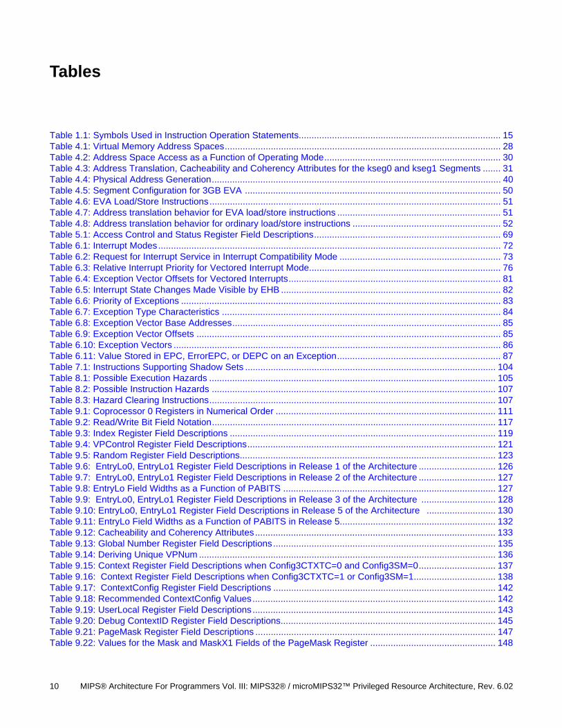
Table 1.1: Symbols Used in Instruction Operation Statements............................................................................... 15Table 4.1: Virtual Memory Address Spaces............................................................................................................ 28Table 4.2: Address Space Access as a Function of Operating Mode..................................................................... 30Table 4.3: Address Translation, Cacheability and Coherency Attributes for the kseg0 and kseg1 Segments ....... 31Table 4.4: Physical Address Generation................................................................................................................. 40Table 4.5: Segment Configuration for 3GB EVA .................................................................................................... 50Table 4.6: EVA Load/Store Instructions.................................................................................................................. 51Table 4.7: Address translation behavior for EVA load/store instructions ................................................................ 51Table 4.8: Address translation behavior for ordinary load/store instructions .......................................................... 52Table 5.1: Access Control and Status Register Field Descriptions......................................................................... 69Table 6.1: Interrupt Modes...................................................................................................................................... 72Table 6.2: Request for Interrupt Service in Interrupt Compatibility Mode ............................................................... 73Table 6.3: Relative Interrupt Priority for Vectored Interrupt Mode........................................................................... 76Table 6.4: Exception Vector Offsets for Vectored Interrupts................................................................................... 81Table 6.5: Interrupt State Changes Made Visible by EHB ...................................................................................... 82Table 6.6: Priority of Exceptions ............................................................................................................................. 83Table 6.7: Exception Type Characteristics ............................................................................................................. 84Table 6.8: Exception Vector Base Addresses......................................................................................................... 85Table 6.9: Exception Vector Offsets ....................................................................................................................... 85Table 6.10: Exception Vectors ................................................................................................................................ 86Table 6.11: Value Stored in EPC, ErrorEPC, or DEPC on an Exception................................................................ 87Table 7.1: Instructions Supporting Shadow Sets .................................................................................................. 104Table 8.1: Possible Execution Hazards ................................................................................................................ 105Table 8.2: Possible Instruction Hazards ............................................................................................................... 107Table 8.3: Hazard Clearing Instructions................................................................................................................ 107Table 9.1: Coprocessor 0 Registers in Numerical Order ...................................................................................... 111Table 9.2: Read/Write Bit Field Notation............................................................................................................... 117Table 9.3: Index Register Field Descriptions ........................................................................................................ 119Table 9.4: VPControl Register Field Descriptions................................................................................................. 121Table 9.5: Random Register Field Descriptions.................................................................................................... 123Table 9.6: EntryLo0, EntryLo1 Register Field Descriptions in Release 1 of the Architecture .............................. 126Table 9.7: EntryLo0, EntryLo1 Register Field Descriptions in Release 2 of the Architecture .............................. 127Table 9.8: EntryLo Field Widths as a Function of PABITS ................................................................................... 127Table 9.9: EntryLo0, EntryLo1 Register Field Descriptions in Release 3 of the Architecture ............................. 128Table 9.10: EntryLo0, EntryLo1 Register Field Descriptions in Release 5 of the Architecture ........................... 130Table 9.11: EntryLo Field Widths as a Function of PABITS in Release 5............................................................. 132Table 9.12: Cacheability and Coherency Attributes .............................................................................................. 133Table 9.13: Global Number Register Field Descriptions....................................................................................... 135Table 9.14: Deriving Unique VPNum .................................................................................................................... 136Table 9.15: Context Register Field Descriptions when Config3CTXTC=0 and Config3SM=0.............................. 137Table 9.16: Context Register Field Descriptions when Config3CTXTC=1 or Config3SM=1................................ 138Table 9.17: ContextConfig Register Field Descriptions ....................................................................................... 142Table 9.18: Recommended ContextConfig Values............................................................................................... 142Table 9.19: UserLocal Register Field Descriptions............................................................................................... 143Table 9.20: Debug ContextID Register Field Descriptions.................................................................................... 145Table 9.21: PageMask Register Field Descriptions .............................................................................................. 147Table 9.22: Values for the Mask and MaskX1 Fields of the PageMask Register ................................................. 148
MIPS® Architecture For Programmers Vol. III: MIPS32® / microMIPS32™ Privileged Resource Architecture, Rev. 6.02 11
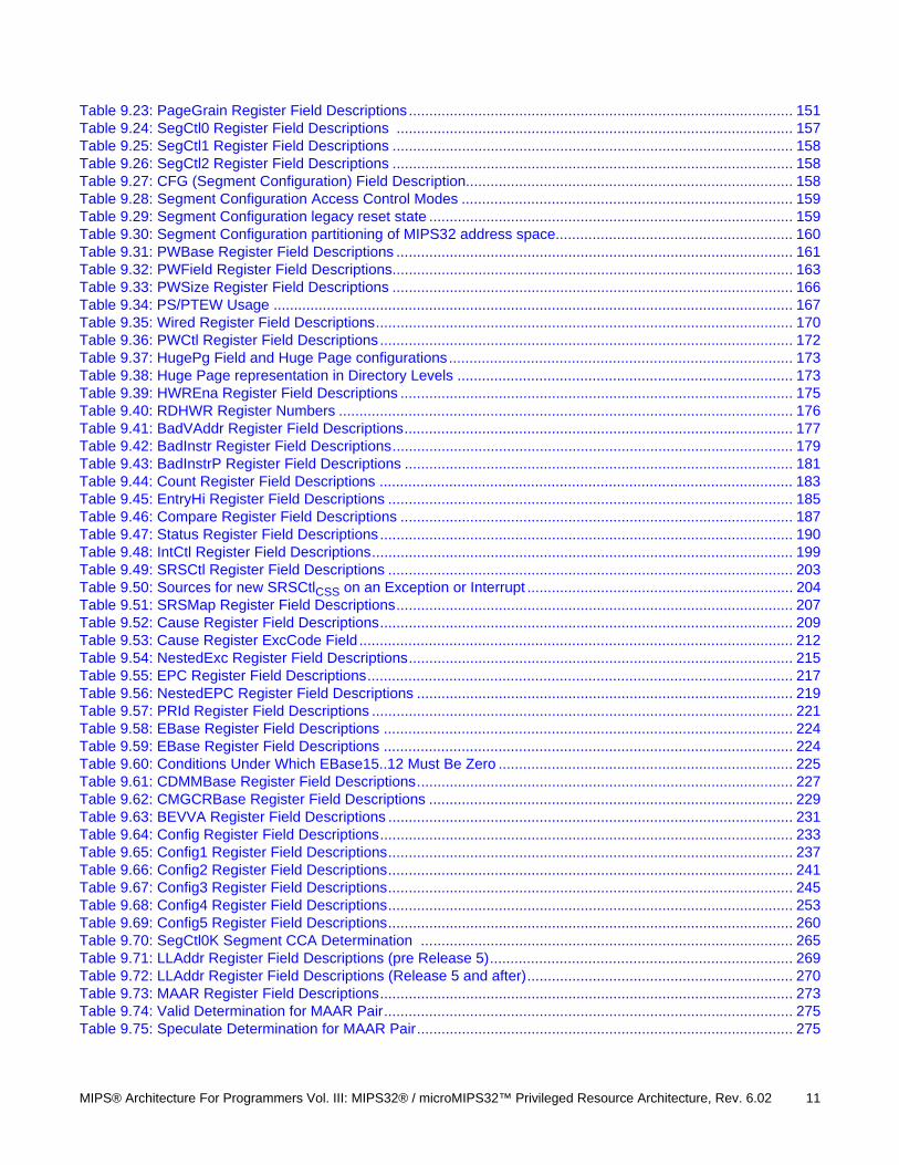
Table 9.23: PageGrain Register Field Descriptions .............................................................................................. 151Table 9.24: SegCtl0 Register Field Descriptions ................................................................................................. 157Table 9.25: SegCtl1 Register Field Descriptions .................................................................................................. 158Table 9.26: SegCtl2 Register Field Descriptions .................................................................................................. 158Table 9.27: CFG (Segment Configuration) Field Description................................................................................ 158Table 9.28: Segment Configuration Access Control Modes ................................................................................. 159Table 9.29: Segment Configuration legacy reset state ......................................................................................... 159Table 9.30: Segment Configuration partitioning of MIPS32 address space.......................................................... 160Table 9.31: PWBase Register Field Descriptions ................................................................................................. 161Table 9.32: PWField Register Field Descriptions.................................................................................................. 163Table 9.33: PWSize Register Field Descriptions .................................................................................................. 166Table 9.34: PS/PTEW Usage ............................................................................................................................... 167Table 9.35: Wired Register Field Descriptions...................................................................................................... 170Table 9.36: PWCtl Register Field Descriptions..................................................................................................... 172Table 9.37: HugePg Field and Huge Page configurations.................................................................................... 173Table 9.38: Huge Page representation in Directory Levels .................................................................................. 173Table 9.39: HWREna Register Field Descriptions ................................................................................................ 175Table 9.40: RDHWR Register Numbers ............................................................................................................... 176Table 9.41: BadVAddr Register Field Descriptions............................................................................................... 177Table 9.42: BadInstr Register Field Descriptions.................................................................................................. 179Table 9.43: BadInstrP Register Field Descriptions ............................................................................................... 181Table 9.44: Count Register Field Descriptions ..................................................................................................... 183Table 9.45: EntryHi Register Field Descriptions ................................................................................................... 185Table 9.46: Compare Register Field Descriptions ................................................................................................ 187Table 9.47: Status Register Field Descriptions..................................................................................................... 190Table 9.48: IntCtl Register Field Descriptions....................................................................................................... 199Table 9.49: SRSCtl Register Field Descriptions ................................................................................................... 203Table 9.50: Sources for new SRSCtlCSS on an Exception or Interrupt ................................................................. 204Table 9.51: SRSMap Register Field Descriptions................................................................................................. 207Table 9.52: Cause Register Field Descriptions..................................................................................................... 209Table 9.53: Cause Register ExcCode Field .......................................................................................................... 212Table 9.54: NestedExc Register Field Descriptions.............................................................................................. 215Table 9.55: EPC Register Field Descriptions........................................................................................................ 217Table 9.56: NestedEPC Register Field Descriptions ............................................................................................ 219Table 9.57: PRId Register Field Descriptions ....................................................................................................... 221Table 9.58: EBase Register Field Descriptions .................................................................................................... 224Table 9.59: EBase Register Field Descriptions .................................................................................................... 224Table 9.60: Conditions Under Which EBase15..12 Must Be Zero ........................................................................ 225Table 9.61: CDMMBase Register Field Descriptions............................................................................................ 227Table 9.62: CMGCRBase Register Field Descriptions ......................................................................................... 229Table 9.63: BEVVA Register Field Descriptions ................................................................................................... 231Table 9.64: Config Register Field Descriptions..................................................................................................... 233Table 9.65: Config1 Register Field Descriptions................................................................................................... 237Table 9.66: Config2 Register Field Descriptions................................................................................................... 241Table 9.67: Config3 Register Field Descriptions................................................................................................... 245Table 9.68: Config4 Register Field Descriptions................................................................................................... 253Table 9.69: Config5 Register Field Descriptions................................................................................................... 260Table 9.70: SegCtl0K Segment CCA Determination ........................................................................................... 265Table 9.71: LLAddr Register Field Descriptions (pre Release 5).......................................................................... 269Table 9.72: LLAddr Register Field Descriptions (Release 5 and after)................................................................. 270Table 9.73: MAAR Register Field Descriptions..................................................................................................... 273Table 9.74: Valid Determination for MAAR Pair.................................................................................................... 275Table 9.75: Speculate Determination for MAAR Pair............................................................................................ 275
12 MIPS® Architecture For Programmers Vol. III: MIPS32® / microMIPS32™ Privileged Resource Architecture, Rev. 6.02
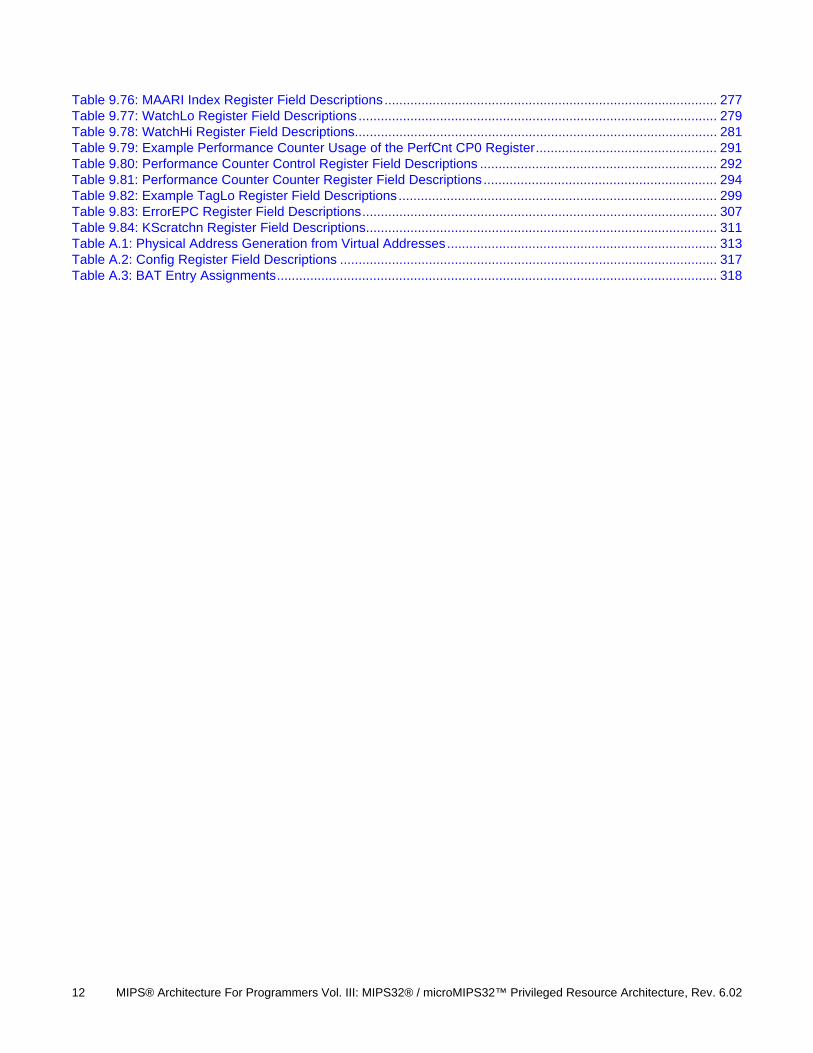
Table 9.76: MAARI Index Register Field Descriptions.......................................................................................... 277Table 9.77: WatchLo Register Field Descriptions................................................................................................. 279Table 9.78: WatchHi Register Field Descriptions.................................................................................................. 281Table 9.79: Example Performance Counter Usage of the PerfCnt CP0 Register................................................. 291Table 9.80: Performance Counter Control Register Field Descriptions ................................................................ 292Table 9.81: Performance Counter Counter Register Field Descriptions............................................................... 294Table 9.82: Example TagLo Register Field Descriptions...................................................................................... 299Table 9.83: ErrorEPC Register Field Descriptions................................................................................................ 307Table 9.84: KScratchn Register Field Descriptions............................................................................................... 311Table A.1: Physical Address Generation from Virtual Addresses......................................................................... 313Table A.2: Config Register Field Descriptions ...................................................................................................... 317Table A.3: BAT Entry Assignments....................................................................................................................... 318
Chapter 1
MIPS® Architecture For Programmers Vol. III: MIPS32® / microMIPS32™ Privileged Resource Architecture, Rev. 6.02 13
About This Book
The MIPS® Architecture For Programmers Vol. III: MIPS32® / microMIPS32™ Privileged Resource Architecture consists of the following documents:
• Volume I-A describes conventions used throughout the document set, and provides an introduction to the MIPS32® Architecture
• Volume I-B describes conventions used throughout the document set, and provides an introduction to the microMIPS32™ Architecture
• Volume II-A provides detailed descriptions of each instruction in the MIPS32® instruction set
• Volume II-B provides detailed descriptions of each instruction in the microMIPS32™ instruction set
• Volume III describes the MIPS32® and microMIPS32™ Privileged Resource Architecture which defines and governs the behavior of the privileged resources included in a MIPS® processor implementation
• Volume IV-a describes the MIPS16e™ Application-Specific Extension to the MIPS32® Architecture. Beginning with Release 3 of the Architecture, microMIPS is the preferred solution for smaller code size.
• Volume IV-b describes the MDMX™ Application-Specific Extension to the MIPS64® Architecture and microMIPS64™. It is not applicable to the MIPS32® document set nor the microMIPS32™ document set. With Release 5 of the Architecture, MDMX is deprecated. MDMX and MSA can not be implemented at the same time.
• Volume IV-c describes the MIPS-3D® Application-Specific Extension to the MIPS® Architecture
• Volume IV-d describes the SmartMIPS® Application-Specific Extension to the MIPS32® Architecture and the microMIPS32™ Architecture .
• Volume IV-e describes the MIPS® DSP Module to the MIPS® Architecture
• Volume IV-f describes the MIPS® MT Module to the MIPS® Architecture
• Volume IV-h describes the MIPS® MCU Application-Specific Extension to the MIPS® Architecture
• Volume IV-i describes the MIPS® Virtualization Module to the MIPS® Architecture
• Volume IV-j describes the MIPS® SIMD Architecture Module to the MIPS® Architecture
About This Book
14 MIPS® Architecture For Programmers Vol. III: MIPS32® / microMIPS32™ Privileged Resource Architecture, Rev. 6.02
1.1 Typographical Conventions
This section describes the use of italic, bold and courier fonts in this book.
1.1.1 Italic Text
• is used for emphasis
• is used for bits, fields, registers, that are important from a software perspective (for instance, address bits used by software, and programmable fields and registers), and various floating point instruction formats, such as S, D, and PS
• is used for the memory access types, such as cached and uncached
1.1.2 Bold Text
• represents a term that is being defined
• is used for bits and fields that are important from a hardware perspective (for instance, register bits, which are not programmable but accessible only to hardware)
• is used for ranges of numbers; the range is indicated by an ellipsis. For instance, 5..1 indicates numbers 5 through 1
• is used to emphasize UNPREDICTABLE and UNDEFINED behavior, as defined below.
1.1.3 Courier Text
Courier fixed-width font is used for text that is displayed on the screen, and for examples of code and instruction pseudocode.
1.2 UNPREDICTABLE and UNDEFINED
The terms UNPREDICTABLE and UNDEFINED are used throughout this book to describe the behavior of the pro-cessor in certain cases. UNDEFINED behavior or operations can occur only as the result of executing instructions in a privileged mode (i.e., in Kernel Mode or Debug Mode, or with the CP0 usable bit set in the Status register). Unprivileged software can never cause UNDEFINED behavior or operations. Conversely, both privileged and unprivileged software can cause UNPREDICTABLE results or operations.
1.2.1 UNPREDICTABLE
UNPREDICTABLE operations can cause a result to be generated or not. UNPREDICTABLE operations can cause arbitrary exceptions. UNPREDICTABLE results or operations have several implementation restrictions:
• Implementations of operations generating UNPREDICTABLE results must not depend on any data source (memory or internal state) that is inaccessible in the current processor mode.
• UNPREDICTABLE operations must not read, write, or modify the contents of memory or an internal state that is inaccessible in the current processor mode. For example, UNPREDICTABLE operations executed in user
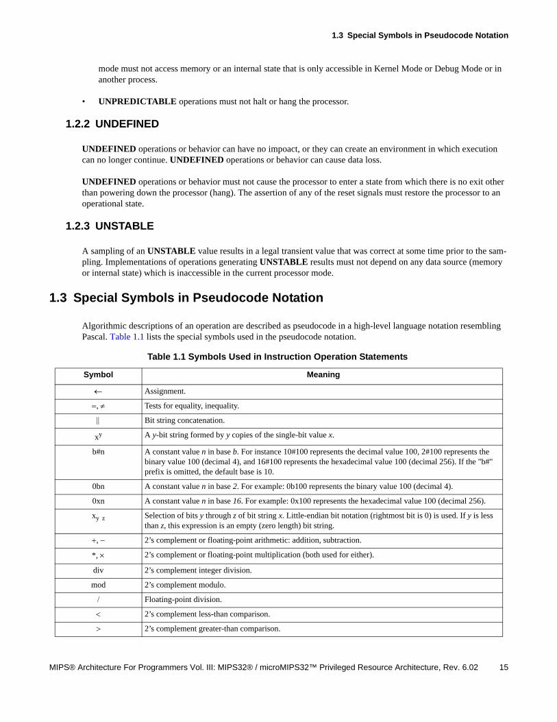
1.3 Special Symbols in Pseudocode Notation
MIPS® Architecture For Programmers Vol. III: MIPS32® / microMIPS32™ Privileged Resource Architecture, Rev. 6.02 15
mode must not access memory or an internal state that is only accessible in Kernel Mode or Debug Mode or in another process.
• UNPREDICTABLE operations must not halt or hang the processor.
1.2.2 UNDEFINED
UNDEFINED operations or behavior can have no impoact, or they can create an environment in which execution can no longer continue. UNDEFINED operations or behavior can cause data loss.
UNDEFINED operations or behavior must not cause the processor to enter a state from which there is no exit other than powering down the processor (hang). The assertion of any of the reset signals must restore the processor to an operational state.
1.2.3 UNSTABLE
A sampling of an UNSTABLE value results in a legal transient value that was correct at some time prior to the sam-pling. Implementations of operations generating UNSTABLE results must not depend on any data source (memory or internal state) which is inaccessible in the current processor mode.
1.3 Special Symbols in Pseudocode Notation
Algorithmic descriptions of an operation are described as pseudocode in a high-level language notation resembling Pascal. Table 1.1 lists the special symbols used in the pseudocode notation.
Table 1.1 Symbols Used in Instruction Operation Statements
Symbol Meaning
Assignment.
, Tests for equality, inequality.
Bit string concatenation.
xy A y-bit string formed by y copies of the single-bit value x.
b#n A constant value n in base b. For instance 10#100 represents the decimal value 100, 2#100 represents the binary value 100 (decimal 4), and 16#100 represents the hexadecimal value 100 (decimal 256). If the "b#" prefix is omitted, the default base is 10.
0bn A constant value n in base 2. For example: 0b100 represents the binary value 100 (decimal 4).
0xn A constant value n in base 16. For example: 0x100 represents the hexadecimal value 100 (decimal 256).
xy z Selection of bits y through z of bit string x. Little-endian bit notation (rightmost bit is 0) is used. If y is less than z, this expression is an empty (zero length) bit string.
, 2’s complement or floating-point arithmetic: addition, subtraction.
*, 2’s complement or floating-point multiplication (both used for either).
div 2’s complement integer division.
mod 2’s complement modulo.
Floating-point division.
2’s complement less-than comparison.
2’s complement greater-than comparison.
About This Book
16 MIPS® Architecture For Programmers Vol. III: MIPS32® / microMIPS32™ Privileged Resource Architecture, Rev. 6.02
2’s complement less-than or equal comparison.
2’s complement greater-than-or-equal comparison.
nor Bitwise logical NOR.
xor Bitwise logical XOR.
and Bitwise logical AND.
or Bitwise logical OR.
not Bitwise inversion.
&& Logical (non-bitwise) AND.
<< Logical shift left (shift in zeros at right-hand-side).
>> Logical shift right (shift in zeros at left-hand-side).
GPRLEN The length, in bits (32 or 64), of the CPU general-purpose registers.
GPR[x] CPU general-purpose register x. The content of GPR[0] is always zero. In Release 2 of the Architecture, GPR[x] is a short-hand notation for SGPR[ SRSCtlCSS, x].
SGPR[s,x] From Release 2 on of the Architecture, multiple copies of the CPU general-purpose registers can be imple-mented. SGPR[s,x] refers to GPR set s, register x.
FPR[x] Floating-point operand register x
FCC[CC] Floating-point condition code CC. FCC[0] has the same value as COC[1].
FPR[x] Floating-point (coprocessor unit 1), general register x
CPR[z,x,s] Coprocessor unit z, general register x, select s.
CP2CPR[x] Coprocessor unit 2, general register x.
CCR[z,x] Coprocessor unit z, control register x.
CP2CCR[x] Coprocessor unit 2, control register x.
COC[z] Coprocessor unit z condition signal.
Xlat[x] Translation of the MIPS16e GPR number x into the corresponding 32-bit GPR number.
BigEndianMem Endian mode as configured at chip reset (0 for little-endian, 1 for big-endian). Specifies the endianness of the memory interface (see LoadMemory and StoreMemory pseudocode function descriptions), and the endian-ness of Kernel and Supervisor mode execution.
BigEndianCPU The endianness for load and store instructions (0 for little-endian, 1 for big-endian). In User mode, this endi-anness can be switched by setting the RE bit in the Status register. Thus, BigEndianCPU can be computed as (BigEndianMem XOR ReverseEndian).
ReverseEndian Signal to reverse the endianness of load and store instructions. This feature is available in User mode only. It is implemented by setting the RE bit of the Status register. Thus, ReverseEndian can be computed as (SRRE
and User mode).
LLbit Bit of virtual state used to specify operation for instructions that provide atomic read-modify-write. LLbit is set when a linked load occurs and is tested by the conditional store. It is cleared (by exception return instruc-tions) during other CPU operation, when a store to the location is no longer atomic.
Table 1.1 Symbols Used in Instruction Operation Statements (Continued)
Symbol Meaning
1.3 Special Symbols in Pseudocode Notation
MIPS® Architecture For Programmers Vol. III: MIPS32® / microMIPS32™ Privileged Resource Architecture, Rev. 6.02 17
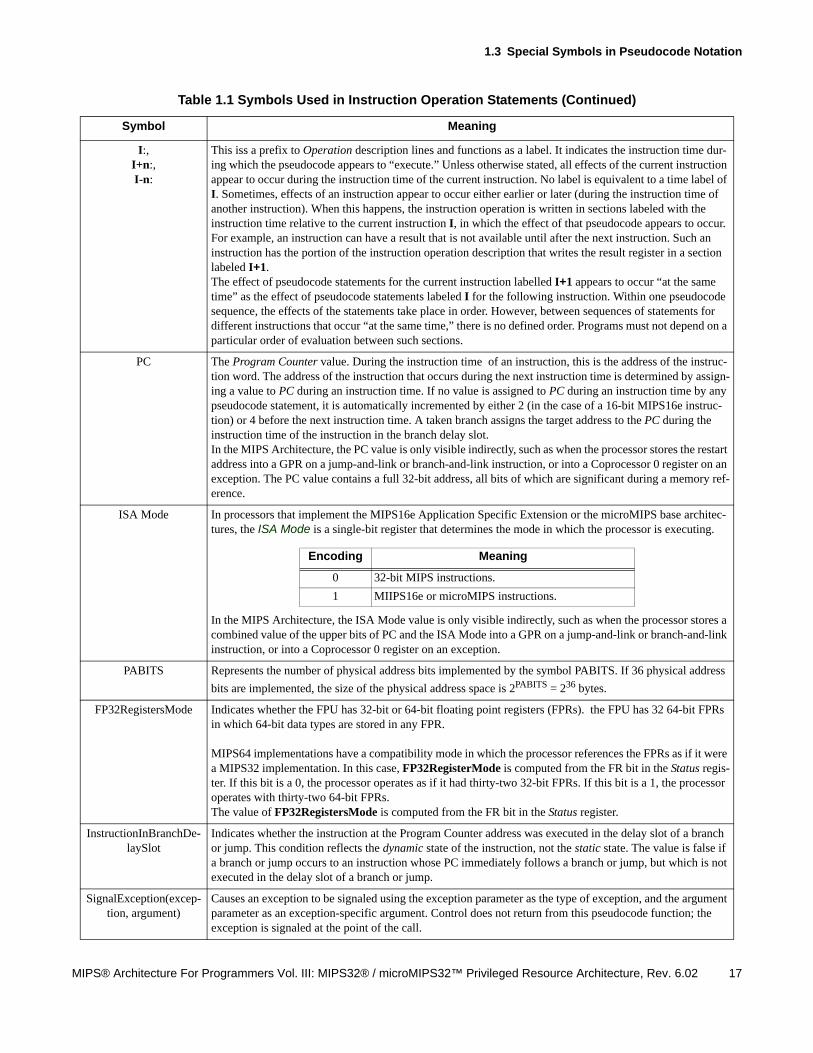
I:,I+n:,I-n:
This iss a prefix to Operation description lines and functions as a label. It indicates the instruction time dur-ing which the pseudocode appears to “execute.” Unless otherwise stated, all effects of the current instruction appear to occur during the instruction time of the current instruction. No label is equivalent to a time label of I. Sometimes, effects of an instruction appear to occur either earlier or later (during the instruction time of another instruction). When this happens, the instruction operation is written in sections labeled with the instruction time relative to the current instruction I, in which the effect of that pseudocode appears to occur. For example, an instruction can have a result that is not available until after the next instruction. Such an instruction has the portion of the instruction operation description that writes the result register in a section labeled I+1.The effect of pseudocode statements for the current instruction labelled I+1 appears to occur “at the same time” as the effect of pseudocode statements labeled I for the following instruction. Within one pseudocode sequence, the effects of the statements take place in order. However, between sequences of statements for different instructions that occur “at the same time,” there is no defined order. Programs must not depend on a particular order of evaluation between such sections.
PC The Program Counter value. During the instruction time of an instruction, this is the address of the instruc-tion word. The address of the instruction that occurs during the next instruction time is determined by assign-ing a value to PC during an instruction time. If no value is assigned to PC during an instruction time by any pseudocode statement, it is automatically incremented by either 2 (in the case of a 16-bit MIPS16e instruc-tion) or 4 before the next instruction time. A taken branch assigns the target address to the PC during the instruction time of the instruction in the branch delay slot.In the MIPS Architecture, the PC value is only visible indirectly, such as when the processor stores the restart address into a GPR on a jump-and-link or branch-and-link instruction, or into a Coprocessor 0 register on an exception. The PC value contains a full 32-bit address, all bits of which are significant during a memory ref-erence.
ISA Mode In processors that implement the MIPS16e Application Specific Extension or the microMIPS base architec-tures, the ISA Mode is a single-bit register that determines the mode in which the processor is executing.
In the MIPS Architecture, the ISA Mode value is only visible indirectly, such as when the processor stores a combined value of the upper bits of PC and the ISA Mode into a GPR on a jump-and-link or branch-and-link instruction, or into a Coprocessor 0 register on an exception.
PABITS Represents the number of physical address bits implemented by the symbol PABITS. If 36 physical address
bits are implemented, the size of the physical address space is 2PABITS = 236 bytes.
FP32RegistersMode Indicates whether the FPU has 32-bit or 64-bit floating point registers (FPRs). the FPU has 32 64-bit FPRs in which 64-bit data types are stored in any FPR.
MIPS64 implementations have a compatibility mode in which the processor references the FPRs as if it were a MIPS32 implementation. In this case, FP32RegisterMode is computed from the FR bit in the Status regis-ter. If this bit is a 0, the processor operates as if it had thirty-two 32-bit FPRs. If this bit is a 1, the processor operates with thirty-two 64-bit FPRs.The value of FP32RegistersMode is computed from the FR bit in the Status register.
InstructionInBranchDe-laySlot
Indicates whether the instruction at the Program Counter address was executed in the delay slot of a branch or jump. This condition reflects the dynamic state of the instruction, not the static state. The value is false if a branch or jump occurs to an instruction whose PC immediately follows a branch or jump, but which is not executed in the delay slot of a branch or jump.
SignalException(excep-tion, argument)
Causes an exception to be signaled using the exception parameter as the type of exception, and the argument parameter as an exception-specific argument. Control does not return from this pseudocode function; the exception is signaled at the point of the call.
Table 1.1 Symbols Used in Instruction Operation Statements (Continued)
Symbol Meaning
Encoding Meaning
0 32-bit MIPS instructions.
1 MIIPS16e or microMIPS instructions.
About This Book
18 MIPS® Architecture For Programmers Vol. III: MIPS32® / microMIPS32™ Privileged Resource Architecture, Rev. 6.02
1.4 For More Information
Various MIPS RISC processor manuals and additional information about MIPS products can be found at the MIPS URL: http://www mips.com
For comments or questions on the MIPS32® Architecture or this document, send email to [email protected].
Chapter 2
MIPS® Architecture For Programmers Vol. III: MIPS32® / microMIPS32™ Privileged Resource Architecture, Rev. 6.02 19
The MIPS32 and microMIPS32 Privileged Resource Architecture
2.1 Introduction
The MIPS32 and microMIPS32 Privileged Resource Architecture (PRA) provides the mechanisms to manage the resources of the CPU: virtual memory, caches, exceptions, and user contexts. The effects of some components of the PRA, such as the virtual memory layout, are user-visible. Many other components are visible only to the operating system kernel and to systems programmers.
2.2 The MIPS Coprocessor Model
The MIPS ISA provides for up to four coprocessors. A coprocessor extends the functionality of the MIPS ISA, while sharing the instruction fetch and execution control logic of the CPU. Some coprocessors, such as the system copro-cessor and the floating-point unit, are standard parts of the ISA and are specified as such in the architecture docu-ments. Coprocessors are generally optional, with one exception: CP0, the system coprocessor, is required. CP0 is the ISA interface to the PRA and provides full control of the processor state and modes.
2.2.1 CP0 - The System Coprocessor
CP0 provides an abstraction of the functions necessary to support an operating system: exception handling, memory management, scheduling, and control of critical resources. The interface to CP0 is through various instructions encoded with the COP0 opcode, including the ability to move data to, and from, the CP0 registers, as well as specific functions that modify CP0 state. The CP0 registers and the interaction with them make up much of the PRA.
2.2.2 CP0 Registers
The CP0 registers provide the interface between the ISA and the PRA. The CP0 registers are described in Chapter 9, “Coprocessor 0 Registers” on page 111.
The MIPS32 and microMIPS32 Privileged Resource Architecture
20 MIPS® Architecture For Programmers Vol. III: MIPS32® / microMIPS32™ Privileged Resource Architecture, Rev. 6.02
Chapter 3
MIPS® Architecture For Programmers Vol. III: MIPS32® / microMIPS32™ Privileged Resource Architecture, Rev. 6.02 21
MIPS32 and microMIPS32 Operating Modes
The MIPS32 and microMIPS32 PRA requires two operating modes: User Mode and Kernel Mode. In User Mode, the programmer can access the CPU and FPU registers that are provided by the ISA, as well as a flat, uniform virtual memory address space. In Kernel Mode, the system programmer can access the full capabilities of the processor, as well as change the virtual memory mapping, control the system environment, and context switch between processes.
The MIPS PRA also supports the implementation of two additional modes: Supervisor Mode and EJTAG Debug Mode. See the EJTAG specification for a description of Debug Mode.
Release 2 of the MIPS32 Architecture added support for 64-bit coprocessors (and, in particular, 64-bit floating-point units) with 32-bit CPUs. Thus, certain floating-point instructions that previously were enabled by 64-bit operations on a MIPS64 processor now are enabled by new 64-bit floating-point operations. Release 3 introduced the micro-MIPS instruction set, allowing all microMIPS processors to implement a 64-bit floating-point unit.
3.1 Debug Mode
For processors that implement EJTAG, the processor is operating in Debug Mode if the DM bit in the CP0 Debug reg-ister is 1. If the processor is in Debug Mode, it has full access to all resources that are available to Kernel Mode oper-ations.
3.2 Kernel Mode
The processor is in Kernel Mode when the DM bit in the Debug register is 0 (if the processor implements Debug Mode), and any of the following is true:
• The KSU field in the CP0 Status register contains 0b00.
• The EXL bit in the Status register is 1.
• The ERL bit in the Status register is 1.
The processor enters Kernel Mode at power-up, or as the result of an interrupt, exception, or error. The processor leaves Kernel Mode and enters User Mode or Supervisor Mode when all of the previous three conditions are false, usually as the result of an ERET instruction.
3.3 Supervisor Mode
The processor is operating in Supervisor Mode (if that optional mode is implemented by the processor) when all of the following are true:
• The DM bit in the Debug register is 0 (if the processor implements Debug Mode).
MIPS32 and microMIPS32 Operating Modes
22 MIPS® Architecture For Programmers Vol. III: MIPS32® / microMIPS32™ Privileged Resource Architecture, Rev. 6.02
• The KSU field in the Status register contains 0b01.
• The EXL and ERL bits in the Status register are both 0.
3.4 User Mode
The processor is operating in User Mode when all of the following are true:
• The DM bit in the Debug register is 0 (if the processor implements Debug Mode).
• The KSU field in the Status register contains 0b10.
• The EXL and ERL bits in the Status register are both 0.
3.5 Other Modes
3.5.1 64-bit Floating-Point Operations Enable
Instructions that are implemented by a 64-bit floating-point unit are legal under any of the following conditions:
• In an implementation of Release 1 of the Architecture, 64-bit floating-point operations are never {{Verify}} enabled in a MIPS32 processor.
• In an implementation of Release 2 or later of the , 64-bit floating-point operations are enabled if the F64 bit in the FIR register is 1. The processor must also implement the floating-point data type. Release 3 introduced the microMIPS instruction set; on all microMIPS processors, 64-bit floating-point operations are enabled if the F64 bit in the FIR register is 1.
3.5.2 64-bit FPR Enable
Access to 64-bit FPRs is controlled by the FR bit in the Status register. If the FR bit is 1, the FPRs are interpreted as thirty-two 64-bit registers that can contain any data type. If the FR bit is 0, the FPRs are interpreted as thirty-two 32-bit registers, any of which can contain a 32-bit data type (W, S). In this case, 64-bit data types are contained in even-odd pairs of registers.
In Release 1 of the Architecture , 64-bit FPRs are supported in a MIPS64 processor. In Release 2 of the Architecture, 64-bit FPRs are supported in a 64-bit floating-point unit, for both MIPS32 and MIPS64 processors. From Release 3 and later of the Architecture, 64-bit FPRs are supported for all processors, including all microMIPS processors. As of Release 5 of the Architecture, if floating-point is implemented, then FR=1 is required; that is, the 64-bit FPU, with the FR=1 64-bit FPU register model, is required. The FR=0 32-bit FPU register model continues to be required.
The operation of the processor is UNPREDICTABLE under the following conditions:
• The FR bit is 0, 64-bit operations are enabled, and a floating-point instruction is executed whose datatype is L or PS.
• The FR bit is 0, and an odd register is referenced by an instruction whose datatype is 64 bits.
3.5 Other Modes
MIPS® Architecture For Programmers Vol. III: MIPS32® / microMIPS32™ Privileged Resource Architecture, Rev. 6.02 23
3.5.3 Coprocessor 0 Enable
Access to Coprocessor 0 registers are enabled under any of the following conditions:
• The processor is running in Kernel Mode or Debug Mode, as defined above.
• The CU0 bit in the Status register is 1.
3.5.4 ISA Mode
Release 3 of the Architecture introduced a second branch of the instruction set family, microMIPS32. Devices can implement both ISA branches (MIPS32 and microMIPS32) or only one branch.
The ISA Mode bit is used to specify which ISA branch to use when decoding instructions. This bit is normally not visible to software. Its value is saved to any GPR used as a jump target address, such as GPR31 when written by a JAL instruction, or the source register for a JR instruction.
For processors that implement the MIPS32 ISA, the ISA Mode bit value of zero selects MIPS32. For processors that implement the microMIPS32 ISA, the ISA Mode bit value of 1 selects microMIPS32. For processors that implement
the MIPS16e™ ASE, the ISA Mode bit value of 1 selects MIPS16e. A processor is not allowed to implement both MIPS16e and microMIPS.
Please read Volume II-B: Introduction to the microMIPS32 Instruction Set, Section 5.3, “ISA Mode Switch” for a detailed description of ISA mode switching between the ISA branches and the ISA Mode bit.
MIPS32 and microMIPS32 Operating Modes
24 MIPS® Architecture For Programmers Vol. III: MIPS32® / microMIPS32™ Privileged Resource Architecture, Rev. 6.02
Chapter 4
MIPS® Architecture For Programmers Vol. III: MIPS32® / microMIPS32™ Privileged Resource Architecture, Rev. 6.02 25
Virtual Memory
4.1 Differences between Releases of the Architecture
4.1.1 Virtual Memory
In Release 1 of the Architecture, the minimum page size was 4 kB, with optional support for pages as large as 256 MB. In Release 2 of the Architecture (and subsequent releases), optional support for 1 kB pages was added for use in specific embedded applications that require access to pages smaller than 4 kB. Such usage is expected to be in conjunction with a default page size of 4 kB and is not intended, or suggested, to replace the default 4 kB page size; rather, to augment it.
Support for 1 kB pages involves the following changes:
• Addition of the PageGrain register. This register is also used by the SmartMIPS™ ASE specification, but bits used by Release 2 of the Architecture and those used by the SmartMIPS ASE specification do not overlap.
• Modification of the EntryHi register to enable writes to, and use of, bits 12..11 (VPN2X).
• Modification of the PageMask register to enable writes to, and use of, bits 12..11 (MaskX).
• Modification of the EntryLo0 and EntryLo1 registers to shift the Config3SP field to the left by two bits, when 1 kB
page support is enabled, to create space for two lower-order physical address bits.
Support for 1 kB pages is denoted by the Config3SP bit; it is enabled by the PageGrainESP bit.
4.1.2 Protection of Virtual Memory Pages
In Release 3 of the Architecture, two optional control bits are added to each TLB entry. These bits, RI (Read Inhibit) and XI (Execute Inhibit), allow more types of protection to be used for virtual pages, including write-only pages and non-executable pages.
This feature originated in the SmartMIPS ASE but has been modified from the original SmartMIPS definition. For the Release 3 version of this feature, each of the RI and XI bits can be separately implemented. For the Release 3 ver-sion of this feature, new exception codes are used when a TLB access does not obey the RI /XI bits.
4.1.3 Context Register
In Release 3 of the Architecture, the Context register is a read/write register containing a address pointer to an arbi-trary power-of-two aligned data structure in memory, such as an entry in the page table entry (PTE) array. In Releases 1 and 2, this pointer was defined to reference a fixed-sized 16-byte structure in memory within a linear array contain-ing an entry for each even/odd virtual page pair. The Release 3 version of the Context register can be used more gen-erally.
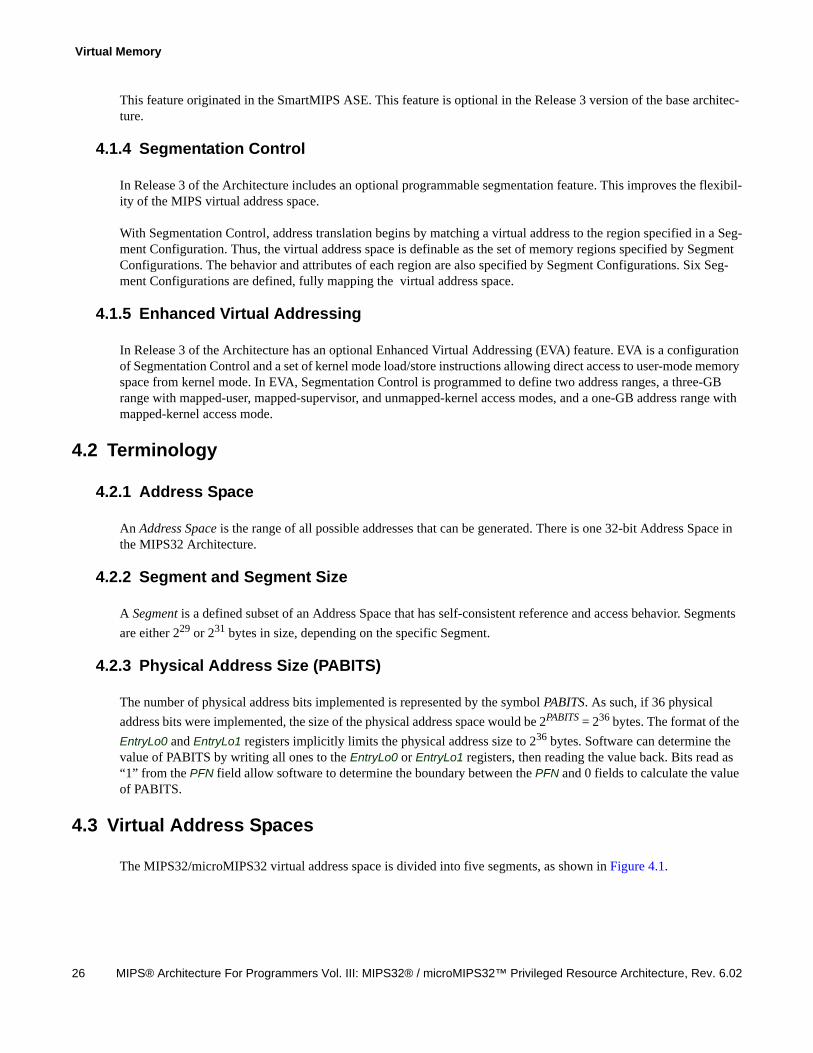
Virtual Memory
26 MIPS® Architecture For Programmers Vol. III: MIPS32® / microMIPS32™ Privileged Resource Architecture, Rev. 6.02
This feature originated in the SmartMIPS ASE. This feature is optional in the Release 3 version of the base architec-ture.
4.1.4 Segmentation Control
In Release 3 of the Architecture includes an optional programmable segmentation feature. This improves the flexibil-ity of the MIPS virtual address space.
With Segmentation Control, address translation begins by matching a virtual address to the region specified in a Seg-ment Configuration. Thus, the virtual address space is definable as the set of memory regions specified by Segment Configurations. The behavior and attributes of each region are also specified by Segment Configurations. Six Seg-ment Configurations are defined, fully mapping the virtual address space.
4.1.5 Enhanced Virtual Addressing
In Release 3 of the Architecture has an optional Enhanced Virtual Addressing (EVA) feature. EVA is a configuration of Segmentation Control and a set of kernel mode load/store instructions allowing direct access to user-mode memory space from kernel mode. In EVA, Segmentation Control is programmed to define two address ranges, a three-GB range with mapped-user, mapped-supervisor, and unmapped-kernel access modes, and a one-GB address range with mapped-kernel access mode.
4.2 Terminology
4.2.1 Address Space
An Address Space is the range of all possible addresses that can be generated. There is one 32-bit Address Space in the MIPS32 Architecture.
4.2.2 Segment and Segment Size
A Segment is a defined subset of an Address Space that has self-consistent reference and access behavior. Segments
are either 229 or 231 bytes in size, depending on the specific Segment.
4.2.3 Physical Address Size (PABITS)
The number of physical address bits implemented is represented by the symbol PABITS. As such, if 36 physical
address bits were implemented, the size of the physical address space would be 2PABITS = 236 bytes. The format of the
EntryLo0 and EntryLo1 registers implicitly limits the physical address size to 236 bytes. Software can determine the value of PABITS by writing all ones to the EntryLo0 or EntryLo1 registers, then reading the value back. Bits read as “1” from the PFN field allow software to determine the boundary between the PFN and 0 fields to calculate the value of PABITS.
4.3 Virtual Address Spaces
The MIPS32/microMIPS32 virtual address space is divided into five segments, as shown in Figure 4.1.
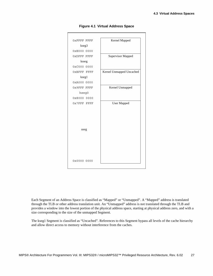
4.3 Virtual Address Spaces
MIPS® Architecture For Programmers Vol. III: MIPS32® / microMIPS32™ Privileged Resource Architecture, Rev. 6.02 27
Figure 4.1 Virtual Address Space
Each Segment of an Address Space is classified as “Mapped” or “Unmapped”. A “Mapped” address is translated through the TLB or other address translation unit. An “Unmapped” address is not translated through the TLB and provides a window into the lowest portion of the physical address space, starting at physical address zero, and with a size corresponding to the size of the unmapped Segment.
The kseg1 Segment is classified as “Uncached”. References to this Segment bypass all levels of the cache hierarchy and allow direct access to memory without interference from the caches.
0xFFFF FFFF Kernel Mapped
kseg3
0xE000 0000
0xDFFF FFFF Supervisor Mapped
ksseg
0xC000 0000
0xBFFF FFFF Kernel Unmapped Uncached
kseg1
0xA000 0000
0x9FFF FFFF Kernel Unmapped
kseg0
0x8000 0000
0x7FFF FFFF User Mapped
useg
0x0000 0000
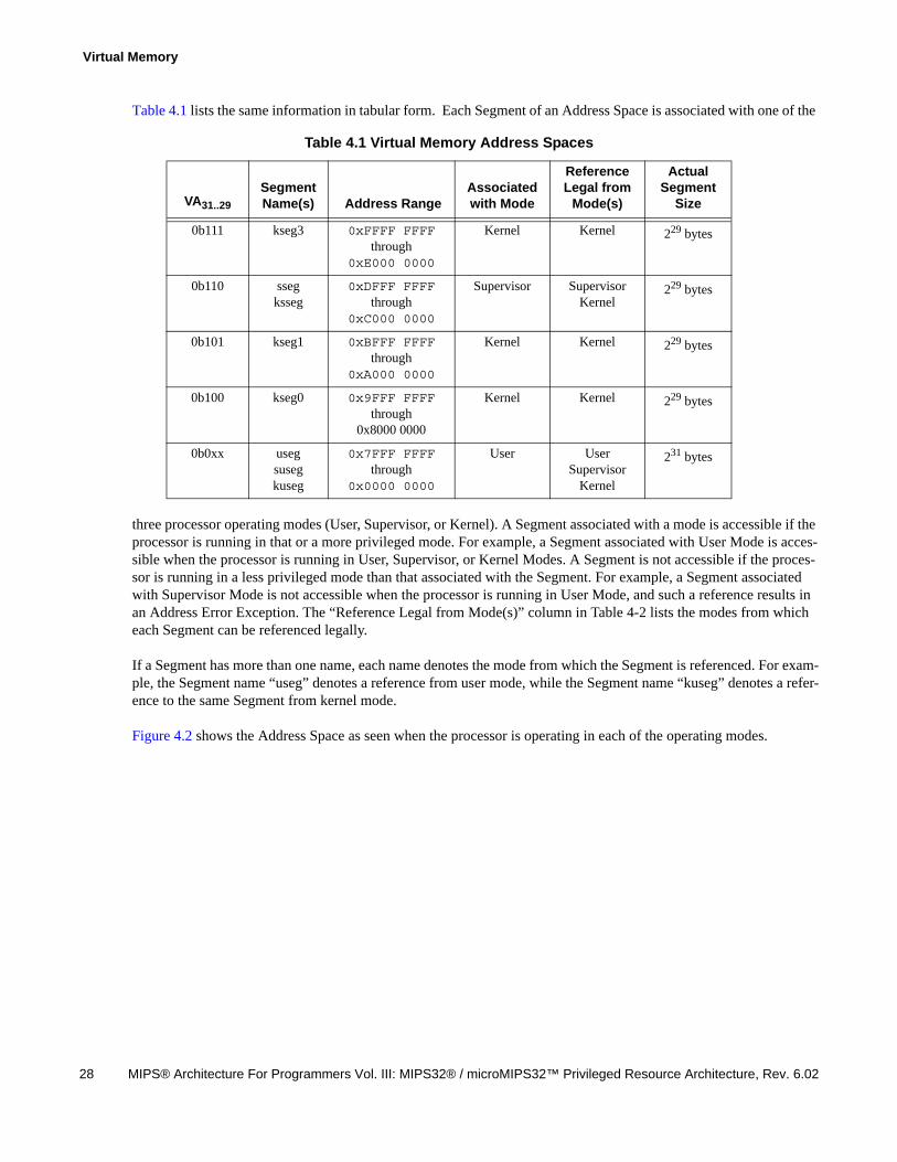
Virtual Memory
28 MIPS® Architecture For Programmers Vol. III: MIPS32® / microMIPS32™ Privileged Resource Architecture, Rev. 6.02
Table 4.1 lists the same information in tabular form. Each Segment of an Address Space is associated with one of the
three processor operating modes (User, Supervisor, or Kernel). A Segment associated with a mode is accessible if the processor is running in that or a more privileged mode. For example, a Segment associated with User Mode is acces-sible when the processor is running in User, Supervisor, or Kernel Modes. A Segment is not accessible if the proces-sor is running in a less privileged mode than that associated with the Segment. For example, a Segment associated with Supervisor Mode is not accessible when the processor is running in User Mode, and such a reference results in an Address Error Exception. The “Reference Legal from Mode(s)” column in Table 4-2 lists the modes from which each Segment can be referenced legally.
If a Segment has more than one name, each name denotes the mode from which the Segment is referenced. For exam-ple, the Segment name “useg” denotes a reference from user mode, while the Segment name “kuseg” denotes a refer-ence to the same Segment from kernel mode.
Figure 4.2 shows the Address Space as seen when the processor is operating in each of the operating modes.
Table 4.1 Virtual Memory Address Spaces
VA31..29
Segment Name(s) Address Range
Associated with Mode
Reference Legal from
Mode(s)
Actual Segment
Size
0b111 kseg3 0xFFFF FFFFthrough
0xE000 0000
Kernel Kernel 229 bytes
0b110 ssegksseg
0xDFFF FFFFthrough
0xC000 0000
Supervisor SupervisorKernel
229 bytes
0b101 kseg1 0xBFFF FFFFthrough
0xA000 0000
Kernel Kernel 229 bytes
0b100 kseg0 0x9FFF FFFFthrough
0x8000 0000
Kernel Kernel 229 bytes
0b0xx usegsusegkuseg
0x7FFF FFFFthrough
0x0000 0000
User UserSupervisor
Kernel
231 bytes
4.4 Compliance
MIPS® Architecture For Programmers Vol. III: MIPS32® / microMIPS32™ Privileged Resource Architecture, Rev. 6.02 29
Figure 4.2 References as a Function of Operating Mode
4.4 Compliance
A MIPS32/microMIPS32 compliant processor must implement the following Segments:
• useg/kuseg
• kseg0
• kseg1
A MIPS32/microMIPS32-compliant processor using TLB-based address translation also must implement the kseg3 Segment.
Figure 4.3 References as a Function of Operating Mode
User Mode References Supervisor Mode References Kernel Mode References
0xFFFF FFFF Address Error 0xFFFF FFFF Address Error 0xFFFF FFFF Kernel Mapped
kseg3
0xE000 0000 0xE000 0000
0xDFFF FFFF Supervisor Mapped 0xDFFF FFFF Supervisor Mapped
sseg ksseg
0xC000 0000 0xC000 0000
0xBFFF FFFF Address Error 0xBFFF FFFF Kernel Unmapped Uncachedkseg1
0xA000 0000
0x9FFF FFFF Kernel Unmapped
kseg0
0x8000 0000 0x8000 0000 0x8000 0000
0x7FFF FFFF User Mapped 0x7FFF FFFF User Mapped 0x7FFF FFFF User Mapped
useg suseg kuseg
0x0000 0000 0x0000 0000 0x0000 0000
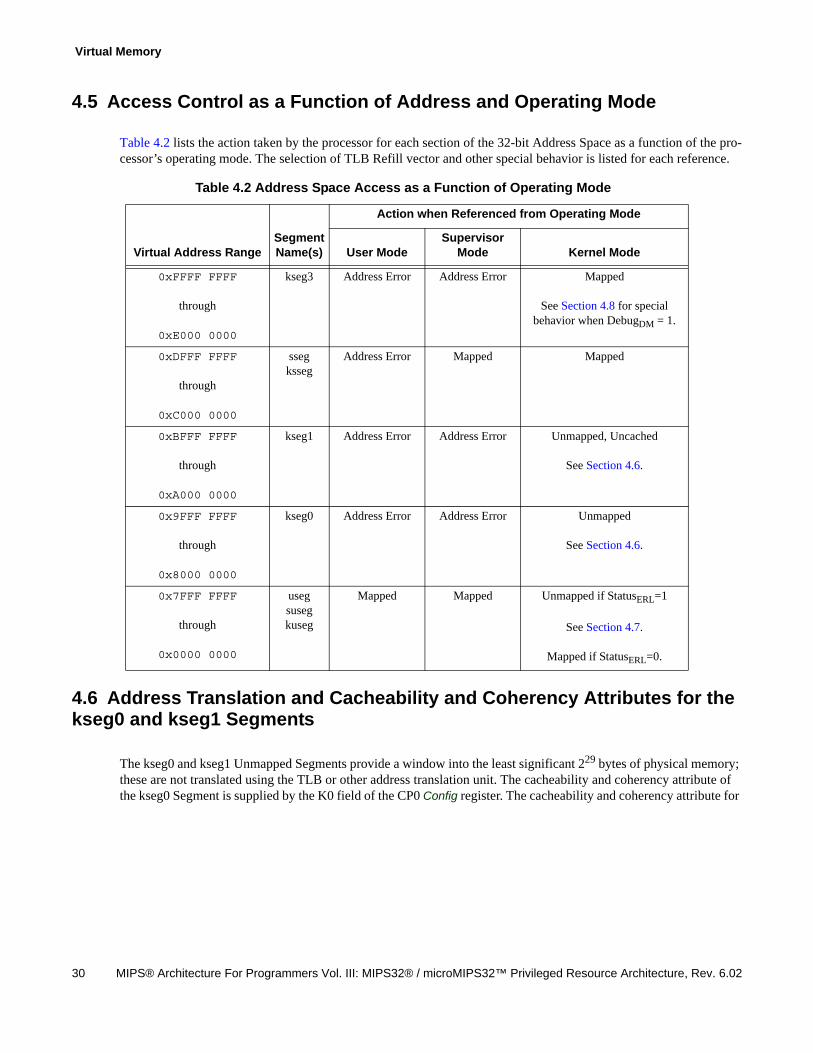
Virtual Memory
30 MIPS® Architecture For Programmers Vol. III: MIPS32® / microMIPS32™ Privileged Resource Architecture, Rev. 6.02
4.5 Access Control as a Function of Address and Operating Mode
Table 4.2 lists the action taken by the processor for each section of the 32-bit Address Space as a function of the pro-cessor’s operating mode. The selection of TLB Refill vector and other special behavior is listed for each reference.
4.6 Address Translation and Cacheability and Coherency Attributes for the kseg0 and kseg1 Segments
The kseg0 and kseg1 Unmapped Segments provide a window into the least significant 229 bytes of physical memory; these are not translated using the TLB or other address translation unit. The cacheability and coherency attribute of the kseg0 Segment is supplied by the K0 field of the CP0 Config register. The cacheability and coherency attribute for
Table 4.2 Address Space Access as a Function of Operating Mode
Virtual Address RangeSegment Name(s)
Action when Referenced from Operating Mode
User ModeSupervisor
Mode Kernel Mode
0xFFFF FFFF
through
0xE000 0000
kseg3 Address Error Address Error Mapped
See Section 4.8 for special behavior when DebugDM = 1.
0xDFFF FFFF
through
0xC000 0000
ssegksseg
Address Error Mapped Mapped
0xBFFF FFFF
through
0xA000 0000
kseg1 Address Error Address Error Unmapped, Uncached
See Section 4.6.
0x9FFF FFFF
through
0x8000 0000
kseg0 Address Error Address Error Unmapped
See Section 4.6.
0x7FFF FFFF
through
0x0000 0000
usegsusegkuseg
Mapped Mapped Unmapped if StatusERL=1
See Section 4.7.
Mapped if StatusERL=0.
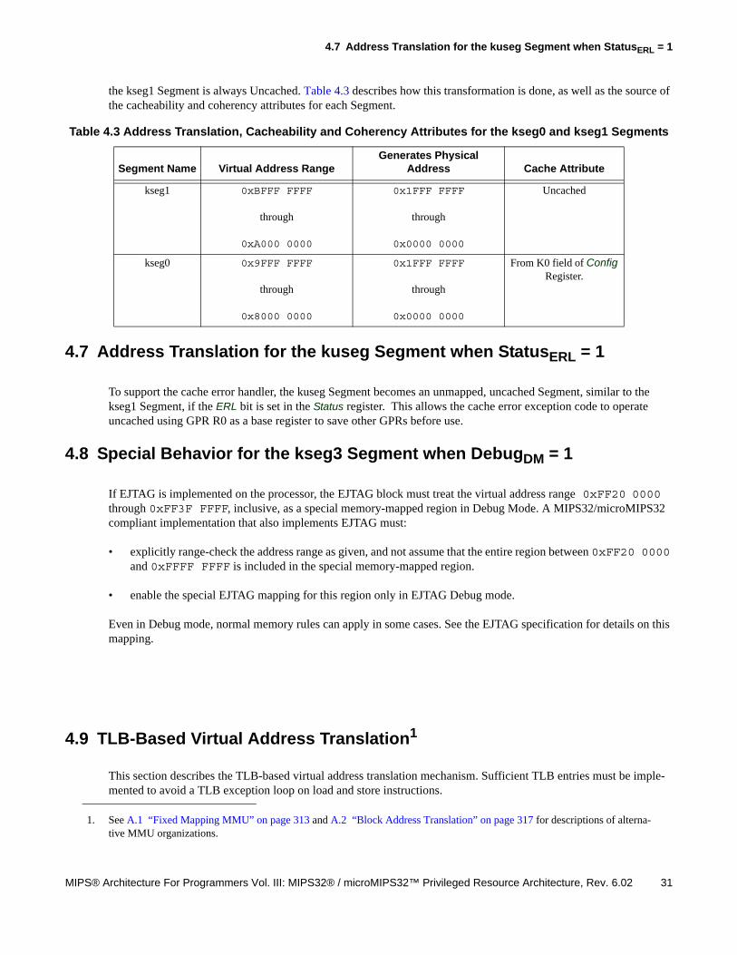
4.7 Address Translation for the kuseg Segment when StatusERL = 1
MIPS® Architecture For Programmers Vol. III: MIPS32® / microMIPS32™ Privileged Resource Architecture, Rev. 6.02 31
the kseg1 Segment is always Uncached. Table 4.3 describes how this transformation is done, as well as the source of the cacheability and coherency attributes for each Segment.
4.7 Address Translation for the kuseg Segment when StatusERL = 1
To support the cache error handler, the kuseg Segment becomes an unmapped, uncached Segment, similar to the kseg1 Segment, if the ERL bit is set in the Status register. This allows the cache error exception code to operate uncached using GPR R0 as a base register to save other GPRs before use.
4.8 Special Behavior for the kseg3 Segment when DebugDM = 1
If EJTAG is implemented on the processor, the EJTAG block must treat the virtual address range 0xFF20 0000 through 0xFF3F FFFF, inclusive, as a special memory-mapped region in Debug Mode. A MIPS32/microMIPS32 compliant implementation that also implements EJTAG must:
• explicitly range-check the address range as given, and not assume that the entire region between 0xFF20 0000 and 0xFFFF FFFF is included in the special memory-mapped region.
• enable the special EJTAG mapping for this region only in EJTAG Debug mode.
Even in Debug mode, normal memory rules can apply in some cases. See the EJTAG specification for details on this mapping.
4.9 TLB-Based Virtual Address Translation1
This section describes the TLB-based virtual address translation mechanism. Sufficient TLB entries must be imple-mented to avoid a TLB exception loop on load and store instructions.
Table 4.3 Address Translation, Cacheability and Coherency Attributes for the kseg0 and kseg1 Segments
Segment Name Virtual Address RangeGenerates Physical
Address Cache Attribute
kseg1 0xBFFF FFFF
through
0xA000 0000
0x1FFF FFFF
through
0x0000 0000
Uncached
kseg0 0x9FFF FFFF
through
0x8000 0000
0x1FFF FFFF
through
0x0000 0000
From K0 field of Config Register.
1. See A.1 “Fixed Mapping MMU” on page 313 and A.2 “Block Address Translation” on page 317 for descriptions of alterna-tive MMU organizations.
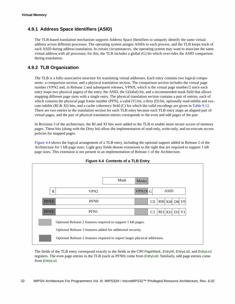
Virtual Memory
32 MIPS® Architecture For Programmers Vol. III: MIPS32® / microMIPS32™ Privileged Resource Architecture, Rev. 6.02
4.9.1 Address Space Identifiers (ASID)
The TLB-based translation mechanism supports Address Space Identifiers to uniquely identify the same virtual address across different processes. The operating system assigns ASIDs to each process, and the TLB keeps track of each ASID during address translation. In certain circumstances, the operating system may want to associate the same virtual address with all processes; for this, the TLB includes a global (G) bit which over-rides the ASID comparison during translation.
4.9.2 TLB Organization
The TLB is a fully-associative structure for translating virtual addresses. Each entry contains two logical compo-nents: a comparison section, and a physical translation section. The comparison section includes the virtual page number (VPN2 and, in Release 2 and subsequent releases, VPNX, which is the virtual page number/2 since each entry maps two physical pages) of the entry, the ASID, the G(lobal) bit, and a recommended mask field that allows mapping different page sizes with a single entry. The physical translation section contains a pair of entries, each of which contains the physical page frame number (PFN), a valid (V) bit, a dirty (D) bit, optionally read-inhibit and exe-cute-inhibit (RI & XI) bits, and a cache coherency field (C) for which the valid encodings are given in Table 9.12. There are two entries in the translation section for each TLB entry because each TLB entry maps an aligned pair of virtual pages, and the pair of physical translation entries corresponds to the even and odd pages of the pair.
In Revision 3 of the architecture, the RI and XI bits were added to the TLB to enable more secure access of memory pages. These bits (along with the Dirty bit) allow the implementation of read-only, write-only, and no-execute access policies for mapped pages.
Figure 4.4 shows the logical arrangement of a TLB entry, including the optional support added in Release 2 of the Architecture for 1 kB page sizes. Light grey fields denote extensions to the right that are required to support 1 kB page sizes. This extension is not present in an implementation of Release 1 of the Architecture.
Figure 4.4 Contents of a TLB Entry
The fields of the TLB entry correspond exactly to the fields in the CP0 PageMask, EntryHi, EntryLo0, and EntryLo1 registers. The even page entries in the TLB (such as PFN0) come from EntryLo0. Similarly, odd page entries come from EntryLo1.
PFNX
G ASIDVPN2
Mask
PFN1 D1 V1RI1 XI1C1
Maskx
VPN2X
PFN0 D0 V0RI0 XI0C0
Optional Release 2 features required to support 1 kB pages.
Optional Release 3 features added for additional security.
PFNX
R
Optional Release 2 features required to suport larger physical addresses.
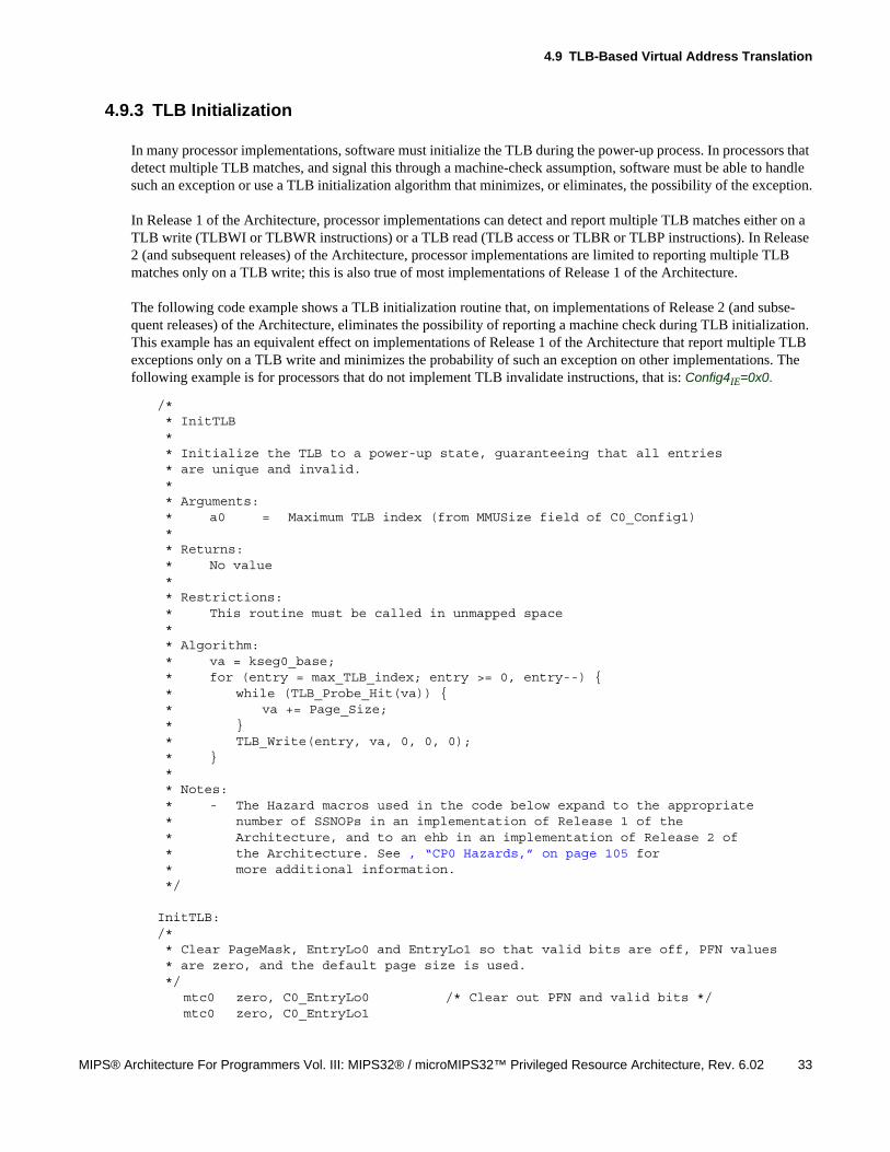
4.9 TLB-Based Virtual Address Translation
MIPS® Architecture For Programmers Vol. III: MIPS32® / microMIPS32™ Privileged Resource Architecture, Rev. 6.02 33
4.9.3 TLB Initialization
In many processor implementations, software must initialize the TLB during the power-up process. In processors that detect multiple TLB matches, and signal this through a machine-check assumption, software must be able to handle such an exception or use a TLB initialization algorithm that minimizes, or eliminates, the possibility of the exception.
In Release 1 of the Architecture, processor implementations can detect and report multiple TLB matches either on a TLB write (TLBWI or TLBWR instructions) or a TLB read (TLB access or TLBR or TLBP instructions). In Release 2 (and subsequent releases) of the Architecture, processor implementations are limited to reporting multiple TLB matches only on a TLB write; this is also true of most implementations of Release 1 of the Architecture.
The following code example shows a TLB initialization routine that, on implementations of Release 2 (and subse-quent releases) of the Architecture, eliminates the possibility of reporting a machine check during TLB initialization. This example has an equivalent effect on implementations of Release 1 of the Architecture that report multiple TLB exceptions only on a TLB write and minimizes the probability of such an exception on other implementations. The following example is for processors that do not implement TLB invalidate instructions, that is: Config4IE=0x0.
/** InitTLB** Initialize the TLB to a power-up state, guaranteeing that all entries* are unique and invalid.** Arguments:* a0 = Maximum TLB index (from MMUSize field of C0_Config1)** Returns:* No value** Restrictions:* This routine must be called in unmapped space** Algorithm:* va = kseg0_base;* for (entry = max_TLB_index; entry >= 0, entry--) {* while (TLB_Probe_Hit(va)) {* va += Page_Size;* }* TLB_Write(entry, va, 0, 0, 0);* }** Notes:* - The Hazard macros used in the code below expand to the appropriate* number of SSNOPs in an implementation of Release 1 of the* Architecture, and to an ehb in an implementation of Release 2 of* the Architecture. See , “CP0 Hazards,” on page 105 for* more additional information.*/
InitTLB:/** Clear PageMask, EntryLo0 and EntryLo1 so that valid bits are off, PFN values* are zero, and the default page size is used.*/
mtc0 zero, C0_EntryLo0 /* Clear out PFN and valid bits */mtc0 zero, C0_EntryLo1
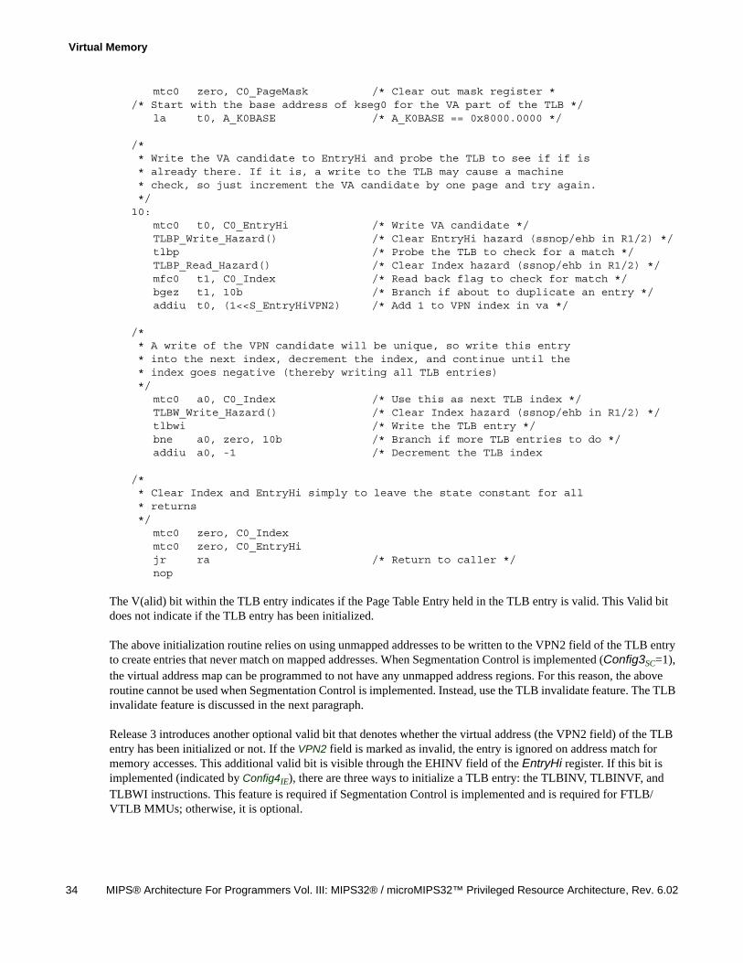
Virtual Memory
34 MIPS® Architecture For Programmers Vol. III: MIPS32® / microMIPS32™ Privileged Resource Architecture, Rev. 6.02
mtc0 zero, C0_PageMask /* Clear out mask register */* Start with the base address of kseg0 for the VA part of the TLB */
la t0, A_K0BASE /* A_K0BASE == 0x8000.0000 */
/** Write the VA candidate to EntryHi and probe the TLB to see if if is* already there. If it is, a write to the TLB may cause a machine* check, so just increment the VA candidate by one page and try again.*/
10:mtc0 t0, C0_EntryHi /* Write VA candidate */TLBP_Write_Hazard() /* Clear EntryHi hazard (ssnop/ehb in R1/2) */tlbp /* Probe the TLB to check for a match */TLBP_Read_Hazard() /* Clear Index hazard (ssnop/ehb in R1/2) */mfc0 t1, C0_Index /* Read back flag to check for match */bgez t1, 10b /* Branch if about to duplicate an entry */addiu t0, (1<<S_EntryHiVPN2) /* Add 1 to VPN index in va */
/** A write of the VPN candidate will be unique, so write this entry* into the next index, decrement the index, and continue until the* index goes negative (thereby writing all TLB entries)*/
mtc0 a0, C0_Index /* Use this as next TLB index */TLBW_Write_Hazard() /* Clear Index hazard (ssnop/ehb in R1/2) */tlbwi /* Write the TLB entry */bne a0, zero, 10b /* Branch if more TLB entries to do */addiu a0, -1 /* Decrement the TLB index
/** Clear Index and EntryHi simply to leave the state constant for all* returns*/
mtc0 zero, C0_Indexmtc0 zero, C0_EntryHijr ra /* Return to caller */nop
The V(alid) bit within the TLB entry indicates if the Page Table Entry held in the TLB entry is valid. This Valid bit does not indicate if the TLB entry has been initialized.
The above initialization routine relies on using unmapped addresses to be written to the VPN2 field of the TLB entry to create entries that never match on mapped addresses. When Segmentation Control is implemented (Config3SC=1), the virtual address map can be programmed to not have any unmapped address regions. For this reason, the above routine cannot be used when Segmentation Control is implemented. Instead, use the TLB invalidate feature. The TLB invalidate feature is discussed in the next paragraph.
Release 3 introduces another optional valid bit that denotes whether the virtual address (the VPN2 field) of the TLB entry has been initialized or not. If the VPN2 field is marked as invalid, the entry is ignored on address match for memory accesses. This additional valid bit is visible through the EHINV field of the EntryHi register. If this bit is implemented (indicated by Config4IE), there are three ways to initialize a TLB entry: the TLBINV, TLBINVF, and TLBWI instructions. This feature is required if Segmentation Control is implemented and is required for FTLB/VTLB MMUs; otherwise, it is optional.
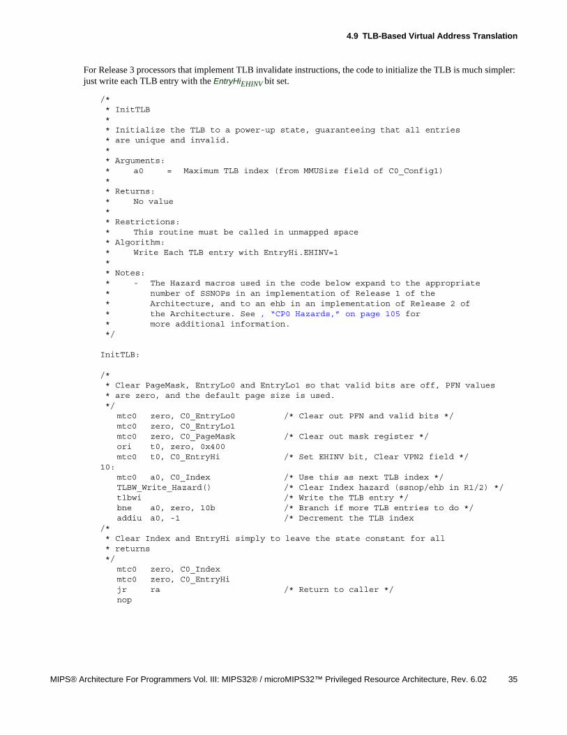
4.9 TLB-Based Virtual Address Translation
MIPS® Architecture For Programmers Vol. III: MIPS32® / microMIPS32™ Privileged Resource Architecture, Rev. 6.02 35
For Release 3 processors that implement TLB invalidate instructions, the code to initialize the TLB is much simpler: just write each TLB entry with the EntryHiEHINV bit set.
/** InitTLB** Initialize the TLB to a power-up state, guaranteeing that all entries* are unique and invalid.** Arguments:* a0 = Maximum TLB index (from MMUSize field of C0_Config1)** Returns:* No value** Restrictions:* This routine must be called in unmapped space* Algorithm:* Write Each TLB entry with EntryHi.EHINV=1** Notes:* - The Hazard macros used in the code below expand to the appropriate* number of SSNOPs in an implementation of Release 1 of the* Architecture, and to an ehb in an implementation of Release 2 of* the Architecture. See , “CP0 Hazards,” on page 105 for* more additional information.*/
InitTLB:
/** Clear PageMask, EntryLo0 and EntryLo1 so that valid bits are off, PFN values* are zero, and the default page size is used.*/
mtc0 zero, C0_EntryLo0 /* Clear out PFN and valid bits */mtc0 zero, C0_EntryLo1mtc0 zero, C0_PageMask /* Clear out mask register */ori t0, zero, 0x400 mtc0 t0, C0_EntryHi /* Set EHINV bit, Clear VPN2 field */
10:mtc0 a0, C0_Index /* Use this as next TLB index */TLBW_Write_Hazard() /* Clear Index hazard (ssnop/ehb in R1/2) */tlbwi /* Write the TLB entry */bne a0, zero, 10b /* Branch if more TLB entries to do */addiu a0, -1 /* Decrement the TLB index
/** Clear Index and EntryHi simply to leave the state constant for all* returns*/
mtc0 zero, C0_Indexmtc0 zero, C0_EntryHijr ra /* Return to caller */nop
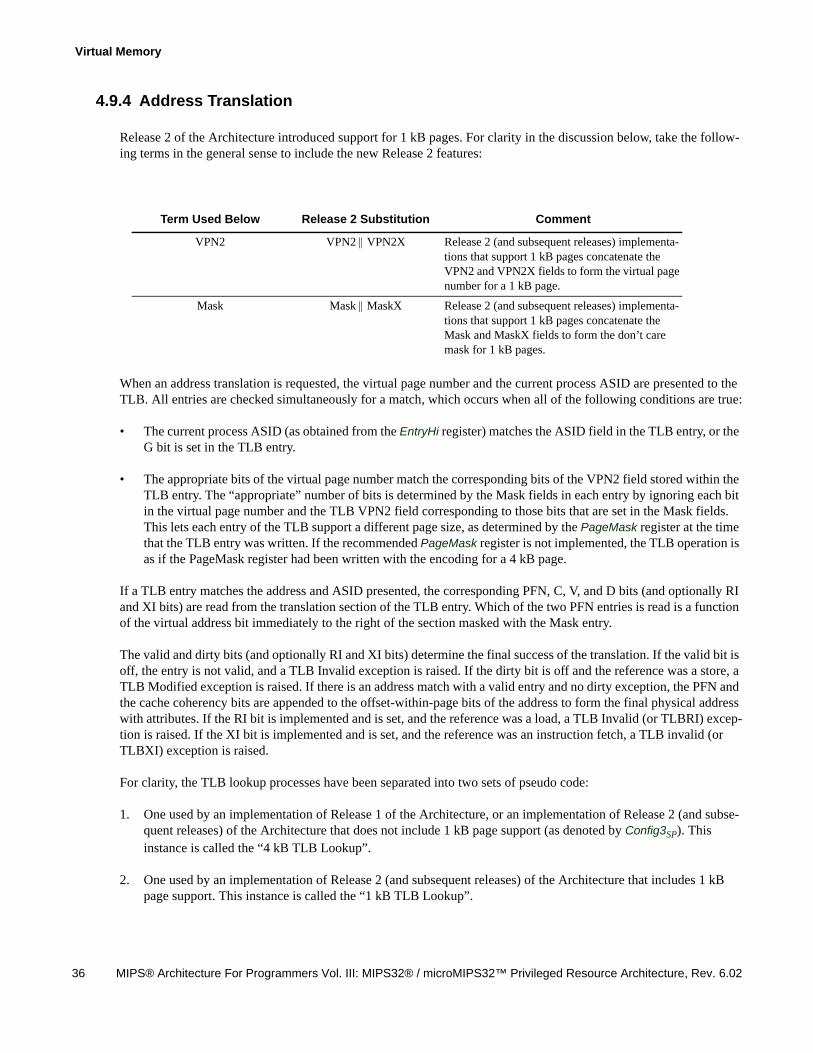
Virtual Memory
36 MIPS® Architecture For Programmers Vol. III: MIPS32® / microMIPS32™ Privileged Resource Architecture, Rev. 6.02
4.9.4 Address Translation
Release 2 of the Architecture introduced support for 1 kB pages. For clarity in the discussion below, take the follow-ing terms in the general sense to include the new Release 2 features:
When an address translation is requested, the virtual page number and the current process ASID are presented to the TLB. All entries are checked simultaneously for a match, which occurs when all of the following conditions are true:
• The current process ASID (as obtained from the EntryHi register) matches the ASID field in the TLB entry, or the G bit is set in the TLB entry.
• The appropriate bits of the virtual page number match the corresponding bits of the VPN2 field stored within the TLB entry. The “appropriate” number of bits is determined by the Mask fields in each entry by ignoring each bit in the virtual page number and the TLB VPN2 field corresponding to those bits that are set in the Mask fields. This lets each entry of the TLB support a different page size, as determined by the PageMask register at the time that the TLB entry was written. If the recommended PageMask register is not implemented, the TLB operation is as if the PageMask register had been written with the encoding for a 4 kB page.
If a TLB entry matches the address and ASID presented, the corresponding PFN, C, V, and D bits (and optionally RI and XI bits) are read from the translation section of the TLB entry. Which of the two PFN entries is read is a function of the virtual address bit immediately to the right of the section masked with the Mask entry.
The valid and dirty bits (and optionally RI and XI bits) determine the final success of the translation. If the valid bit is off, the entry is not valid, and a TLB Invalid exception is raised. If the dirty bit is off and the reference was a store, a TLB Modified exception is raised. If there is an address match with a valid entry and no dirty exception, the PFN and the cache coherency bits are appended to the offset-within-page bits of the address to form the final physical address with attributes. If the RI bit is implemented and is set, and the reference was a load, a TLB Invalid (or TLBRI) excep-tion is raised. If the XI bit is implemented and is set, and the reference was an instruction fetch, a TLB invalid (or TLBXI) exception is raised.
For clarity, the TLB lookup processes have been separated into two sets of pseudo code:
1. One used by an implementation of Release 1 of the Architecture, or an implementation of Release 2 (and subse-quent releases) of the Architecture that does not include 1 kB page support (as denoted by Config3SP). This instance is called the “4 kB TLB Lookup”.
2. One used by an implementation of Release 2 (and subsequent releases) of the Architecture that includes 1 kB page support. This instance is called the “1 kB TLB Lookup”.
Term Used Below Release 2 Substitution Comment
VPN2 VPN2 VPN2X Release 2 (and subsequent releases) implementa-tions that support 1 kB pages concatenate the VPN2 and VPN2X fields to form the virtual page number for a 1 kB page.
Mask Mask MaskX Release 2 (and subsequent releases) implementa-tions that support 1 kB pages concatenate the Mask and MaskX fields to form the don’t care mask for 1 kB pages.
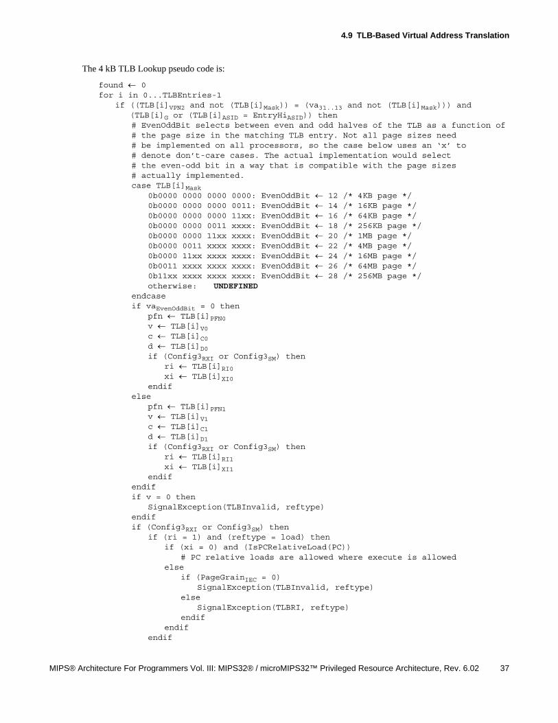
4.9 TLB-Based Virtual Address Translation
MIPS® Architecture For Programmers Vol. III: MIPS32® / microMIPS32™ Privileged Resource Architecture, Rev. 6.02 37
The 4 kB TLB Lookup pseudo code is:
found 0for i in 0...TLBEntries-1
if ((TLB[i]VPN2 and not (TLB[i]Mask)) = (va31..13 and not (TLB[i]Mask))) and (TLB[i]G or (TLB[i]ASID = EntryHiASID)) then
# EvenOddBit selects between even and odd halves of the TLB as a function of# the page size in the matching TLB entry. Not all page sizes need# be implemented on all processors, so the case below uses an ‘x’ to# denote don’t-care cases. The actual implementation would select# the even-odd bit in a way that is compatible with the page sizes# actually implemented.case TLB[i]Mask
0b0000 0000 0000 0000: EvenOddBit 12 /* 4KB page */0b0000 0000 0000 0011: EvenOddBit 14 /* 16KB page */0b0000 0000 0000 11xx: EvenOddBit 16 /* 64KB page */0b0000 0000 0011 xxxx: EvenOddBit 18 /* 256KB page */0b0000 0000 11xx xxxx: EvenOddBit 20 /* 1MB page */0b0000 0011 xxxx xxxx: EvenOddBit 22 /* 4MB page */0b0000 11xx xxxx xxxx: EvenOddBit 24 /* 16MB page */0b0011 xxxx xxxx xxxx: EvenOddBit 26 /* 64MB page */0b11xx xxxx xxxx xxxx: EvenOddBit 28 /* 256MB page */otherwise: UNDEFINED
endcaseif vaEvenOddBit = 0 then
pfn TLB[i]PFN0v TLB[i]V0c TLB[i]C0d TLB[i]D0if (Config3RXI or Config3SM) then
ri TLB[i]RI0xi TLB[i]XI0
endifelse
pfn TLB[i]PFN1v TLB[i]V1c TLB[i]C1d TLB[i]D1if (Config3RXI or Config3SM) then
ri TLB[i]RI1xi TLB[i]XI1
endifendifif v = 0 then
SignalException(TLBInvalid, reftype)endifif (Config3RXI or Config3SM) then
if (ri = 1) and (reftype = load) thenif (xi = 0) and (IsPCRelativeLoad(PC))
# PC relative loads are allowed where execute is allowedelse
if (PageGrainIEC = 0) SignalException(TLBInvalid, reftype)
elseSignalException(TLBRI, reftype)
endifendif
endif
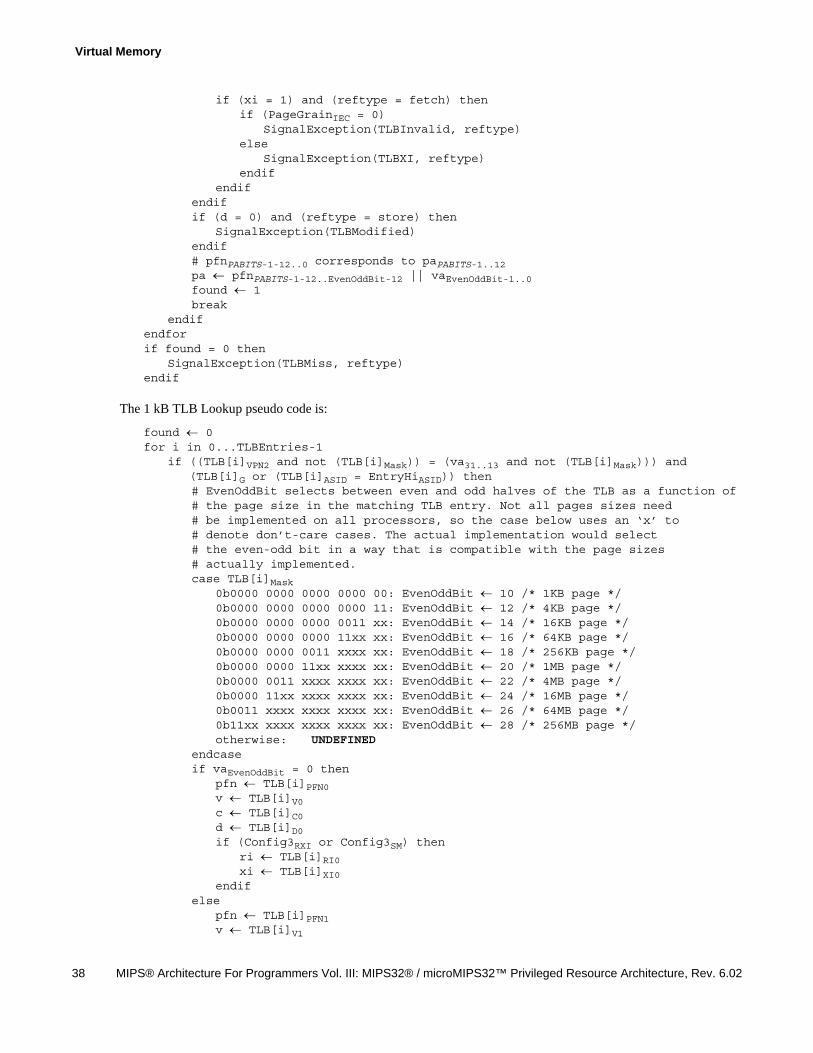
Virtual Memory
38 MIPS® Architecture For Programmers Vol. III: MIPS32® / microMIPS32™ Privileged Resource Architecture, Rev. 6.02
if (xi = 1) and (reftype = fetch) thenif (PageGrainIEC = 0)
SignalException(TLBInvalid, reftype)else
SignalException(TLBXI, reftype)endif
endifendifif (d = 0) and (reftype = store) then
SignalException(TLBModified)endif# pfnPABITS-1-12..0 corresponds to paPABITS-1..12pa pfnPABITS-1-12..EvenOddBit-12 || vaEvenOddBit-1..0found 1break
endifendforif found = 0 then
SignalException(TLBMiss, reftype)endif
The 1 kB TLB Lookup pseudo code is:
found 0for i in 0...TLBEntries-1
if ((TLB[i]VPN2 and not (TLB[i]Mask)) = (va31..13 and not (TLB[i]Mask))) and (TLB[i]G or (TLB[i]ASID = EntryHiASID)) then
# EvenOddBit selects between even and odd halves of the TLB as a function of# the page size in the matching TLB entry. Not all pages sizes need# be implemented on all processors, so the case below uses an ‘x’ to# denote don’t-care cases. The actual implementation would select# the even-odd bit in a way that is compatible with the page sizes# actually implemented.case TLB[i]Mask
0b0000 0000 0000 0000 00: EvenOddBit 10 /* 1KB page */0b0000 0000 0000 0000 11: EvenOddBit 12 /* 4KB page */0b0000 0000 0000 0011 xx: EvenOddBit 14 /* 16KB page */0b0000 0000 0000 11xx xx: EvenOddBit 16 /* 64KB page */0b0000 0000 0011 xxxx xx: EvenOddBit 18 /* 256KB page */0b0000 0000 11xx xxxx xx: EvenOddBit 20 /* 1MB page */0b0000 0011 xxxx xxxx xx: EvenOddBit 22 /* 4MB page */0b0000 11xx xxxx xxxx xx: EvenOddBit 24 /* 16MB page */0b0011 xxxx xxxx xxxx xx: EvenOddBit 26 /* 64MB page */0b11xx xxxx xxxx xxxx xx: EvenOddBit 28 /* 256MB page */otherwise: UNDEFINED
endcaseif vaEvenOddBit = 0 then
pfn TLB[i]PFN0v TLB[i]V0c TLB[i]C0d TLB[i]D0if (Config3RXI or Config3SM) then
ri TLB[i]RI0xi TLB[i]XI0
endifelse
pfn TLB[i]PFN1v TLB[i]V1
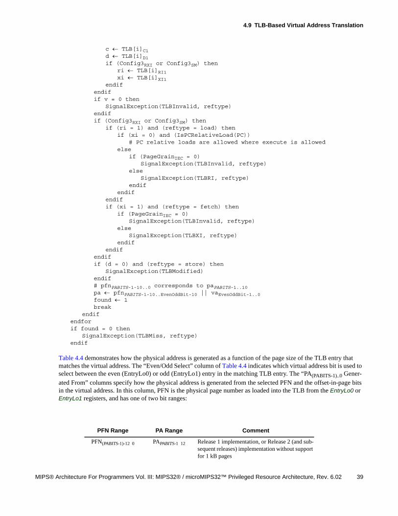
4.9 TLB-Based Virtual Address Translation
MIPS® Architecture For Programmers Vol. III: MIPS32® / microMIPS32™ Privileged Resource Architecture, Rev. 6.02 39
c TLB[i]C1d TLB[i]D1if (Config3RXI or Config3SM) then
ri TLB[i]RI1xi TLB[i]XI1
endifendifif v = 0 then
SignalException(TLBInvalid, reftype)endifif (Config3RXI or Config3SM) then
if (ri = 1) and (reftype = load) thenif (xi = 0) and (IsPCRelativeLoad(PC))
# PC relative loads are allowed where execute is allowedelse
if (PageGrainIEC = 0) SignalException(TLBInvalid, reftype)
elseSignalException(TLBRI, reftype)
endifendif
endifif (xi = 1) and (reftype = fetch) then
if (PageGrainIEC = 0) SignalException(TLBInvalid, reftype)
elseSignalException(TLBXI, reftype)
endifendif
endifif (d = 0) and (reftype = store) then
SignalException(TLBModified)endif# pfnPABITS-1-10..0 corresponds to paPABITS-1..10pa pfnPABITS-1-10..EvenOddBit-10 || vaEvenOddBit-1..0found 1break
endifendforif found = 0 then
SignalException(TLBMiss, reftype)endif
Table 4.4 demonstrates how the physical address is generated as a function of the page size of the TLB entry that matches the virtual address. The “Even/Odd Select” column of Table 4.4 indicates which virtual address bit is used to select between the even (EntryLo0) or odd (EntryLo1) entry in the matching TLB entry. The “PA(PABITS-1)..0 Gener-
ated From” columns specify how the physical address is generated from the selected PFN and the offset-in-page bits in the virtual address. In this column, PFN is the physical page number as loaded into the TLB from the EntryLo0 or EntryLo1 registers, and has one of two bit ranges:
PFN Range PA Range Comment
PFN(PABITS-1)-12 0 PAPABITS-1 12 Release 1 implementation, or Release 2 (and sub-sequent releases) implementation without support for 1 kB pages
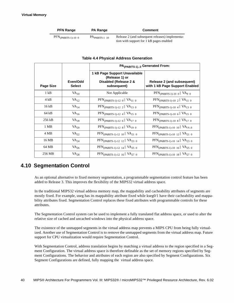
Virtual Memory
40 MIPS® Architecture For Programmers Vol. III: MIPS32® / microMIPS32™ Privileged Resource Architecture, Rev. 6.02
4.10 Segmentation Control
As an optional alternative to fixed memory segmentation, a programmable segmentation control feature has been added to Release 3. This improves the flexibility of the MIPS32 virtual address space.
In the traditional MIPS32 virtual address memory map, the mappability and cacheability attributes of segments are mostly fixed. For example, useg has its mappability attribute fixed while kseg0/1 have their cacheability and mappa-bility attributes fixed. Segmentation Control replaces these fixed attributes with programmable controls for these attributes.
The Segmentation Control system can be used to implement a fully translated flat address space, or used to alter the relative size of cached and uncached windows into the physical address space.
The existence of the unmapped segments in the virtual address map prevents a MIPS CPU from being fully virtual-ized. Another use of Segmentation Control is to remove the unmapped segments from the virtual address map. Future support for CPU virtualization would require Segmentation Control.
With Segmentation Control, address translation begins by matching a virtual address to the region specified in a Seg-ment Configuration. The virtual address space is therefore definable as the set of memory regions specified by Seg-ment Configurations. The behavior and attributes of each region are also specified by Segment Configurations. Six Segment Configurations are defined, fully mapping the virtual address space.
PFN(PABITS-1)-10 0 PAPABITS-1 10 Release 2 (and subsequent releases) implementa-tion with support for 1 kB pages enabled
Table 4.4 Physical Address Generation
Page SizeEven/Odd
Select
PA(PABITS-1)..0 Generated From:
1 kB Page Support Unavailable (Release 1) or
Disabled (Release 2 & subsequent)
Release 2 (and subsequent) with 1 kB Page Support Enabled
1 kB VA10 Not Applicable PFN(PABITS-1)-10 0 VA9 0
4 kB VA12 PFN(PABITS-1)-12 0 VA11 0 PFN(PABITS-1)-10 2 VA11 0
16 kB VA14 PFN(PABITS-1)-12 2 VA13 0 PFN(PABITS-1)-10 4 VA13 0
64 kB VA16 PFN(PABITS-1)-12 4 VA15 0 PFN(PABITS-1)-10 6 VA15 0
256 kB VA18 PFN(PABITS-1)-12 6 VA17 0 PFN(PABITS-1)-10 8 VA17 0
1 MB VA20 PFN(PABITS-1)-12 8 VA19 0 PFN(PABITS-1)-10 10 VA
4 MB VA22 PFN(PABITS-1)-12 10 VA21 0 PFN(PABITS-1)-10 12 VA21 0
16 MB VA24 PFN(PABITS-1)-12 12 VA23 0 PFN(PABITS-1)-10 14 VA23 0
64 MB VA26 PFN(PABITS-1)-12 14 VA25 0 PFN(PABITS-1)-10 16 VA25 0
256 MB VA28 PFN(PABITS-1)-12 16 VA27 0 PFN(PABITS-1)-10 18 VA27 0
PFN Range PA Range Comment
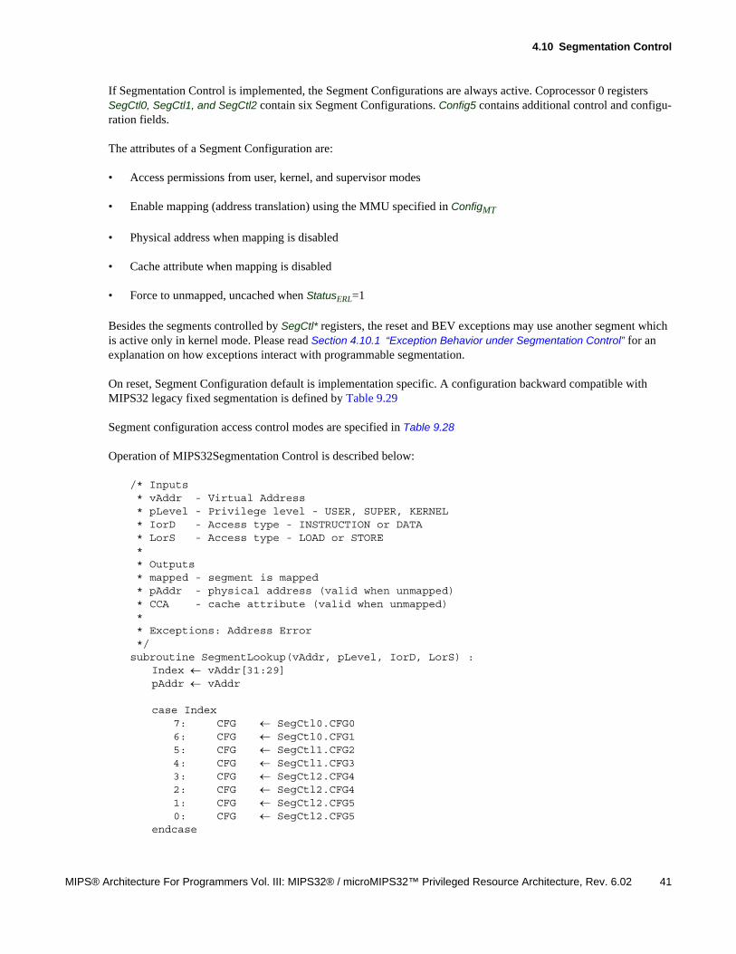
4.10 Segmentation Control
MIPS® Architecture For Programmers Vol. III: MIPS32® / microMIPS32™ Privileged Resource Architecture, Rev. 6.02 41
If Segmentation Control is implemented, the Segment Configurations are always active. Coprocessor 0 registers SegCtl0, SegCtl1, and SegCtl2 contain six Segment Configurations. Config5 contains additional control and configu-ration fields.
The attributes of a Segment Configuration are:
• Access permissions from user, kernel, and supervisor modes
• Enable mapping (address translation) using the MMU specified in ConfigMT
• Physical address when mapping is disabled
• Cache attribute when mapping is disabled
• Force to unmapped, uncached when StatusERL=1
Besides the segments controlled by SegCtl* registers, the reset and BEV exceptions may use another segment which is active only in kernel mode. Please read Section 4.10.1 “Exception Behavior under Segmentation Control” for an explanation on how exceptions interact with programmable segmentation.
On reset, Segment Configuration default is implementation specific. A configuration backward compatible with MIPS32 legacy fixed segmentation is defined by Table 9.29
Segment configuration access control modes are specified in Table 9.28
Operation of MIPS32Segmentation Control is described below:
/* Inputs* vAddr - Virtual Address* pLevel - Privilege level - USER, SUPER, KERNEL* IorD - Access type - INSTRUCTION or DATA* LorS - Access type - LOAD or STORE* * Outputs* mapped - segment is mapped* pAddr - physical address (valid when unmapped)* CCA - cache attribute (valid when unmapped)* * Exceptions: Address Error*/
subroutine SegmentLookup(vAddr, pLevel, IorD, LorS) :Index vAddr[31:29]pAddr vAddr
case Index7: CFG SegCtl0.CFG06: CFG SegCtl0.CFG15: CFG SegCtl1.CFG24: CFG SegCtl1.CFG33: CFG SegCtl2.CFG42: CFG SegCtl2.CFG41: CFG SegCtl2.CFG50: CFG SegCtl2.CFG5
endcase
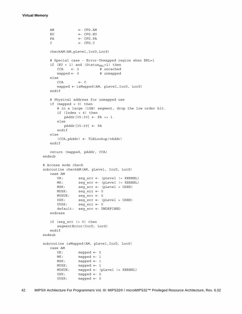
Virtual Memory
42 MIPS® Architecture For Programmers Vol. III: MIPS32® / microMIPS32™ Privileged Resource Architecture, Rev. 6.02
AM CFG.AMEU CFG.EUPA CFG.PAC CFG.C
checkAM(AM,pLevel,IorD,LorS)
# Special case - Error-Unmapped region when ERL=1if (EU = 1) and (StatusERL=1) then
CCA 2 # uncachedmapped 0 # unmapped
elseCCA Cmapped isMapped(AM, pLevel,IorD, LorS)
endif
# Physical address for unmapped useif (mapped = 0) then
# in a large (1GB) segment, drop the low order bit.if (Index < 4) then
pAddr[35:30] PA >> 1else
pAddr[35:29] PAendif
else(CCA,pAddr) TLBLookup(vAddr)
endif
return (mapped, pAddr, CCA)endsub
# Access mode checksubroutine checkAM(AM, pLevel, IorD, LorS)
case AMUK: seg_err (pLevel != KERNEL)MK: seg_err (pLevel != KERNEL)MSK: seg_err (pLevel = USER)MUSK: seg_err 0MUSUK: seg_err 0USK: seg_err (pLevel = USER)UUSK: seg_err 0default: seg_err UNDEFINED
endcase
if (seg_err != 0) thensegmentError(IorD, LorS)
endifendsub
subroutine isMapped(AM, pLevel,IorD, LorS)case AM
UK: mapped 0MK: mapped 1MSK: mapped 1MUSK: mapped 1MUSUK: mapped (pLevel != KERNEL)USK: mapped 0UUSK: mapped 0
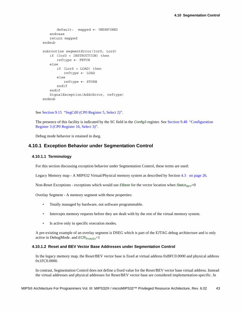
4.10 Segmentation Control
MIPS® Architecture For Programmers Vol. III: MIPS32® / microMIPS32™ Privileged Resource Architecture, Rev. 6.02 43
default: mapped UNDEFINEDendcasereturn mapped
endsub
subroutine segmentError(IorD, LorS)if (IorD = INSTRUCTION) then
reftype FETCHelse
if (LorS = LOAD) thenreftype LOAD
elsereftype STORE
endifendifSignalException(AddrError, reftype)
endsub
See Section 9.15 “SegCtl0 (CP0 Register 5, Select 2)”.
The presence of this facility is indicated by the SC field in the Config3 register. See Section 9.48 “Configuration Register 3 (CP0 Register 16, Select 3)”.
Debug mode behavior is retained in dseg.
4.10.1 Exception Behavior under Segmentation Control
4.10.1.1 Terminology
For this section discussing exception behavior under Segmentation Control, these terms are used:
Legacy Memory map - A MIPS32 Virtual/Physical memory system as described by Section 4.3 on page 26.
Non-Reset Exceptions - exceptions which would use EBase for the vector location when StatusBEV=0
Overlay Segment - A memory segment with these properties:
• Totally managed by hardware, not software programmable.
• Intercepts memory requests before they are dealt with by the rest of the virtual memory system.
• Is active only in specific execution modes.
A pre-existing example of an overlay segment is DSEG which is part of the EJTAG debug architecture and is only active in DebugMode. and ECRProbeEn=1
4.10.1.2 Reset and BEV Vector Base Addresses under Segmentation Control
In the legacy memory map, the Reset/BEV vector base is fixed at virtual address 0xBFC0.0000 and physical address 0x1FC0.0000.
In contrast, Segmentation Control does not define a fixed value for the Reset/BEV vector base virtual address. Instead the virtual addresses and physical addresses for Reset/BEV vector base are considered implementation-specific. In
Virtual Memory
44 MIPS® Architecture For Programmers Vol. III: MIPS32® / microMIPS32™ Privileged Resource Architecture, Rev. 6.02
Segmentation Control, the physical address of Reset/BEV vector does not have to be derived from the virtual address by dropping VA[31:29], other mappings are allowed.
Reset and BEV exceptions - Cacheability and Map-ability
In the legacy memory map, the memory accesses to the Reset/BEV vector region are within KSEG1, which ensures the accesses to this region are always uncached and unmapped.
The architecture requires that the reset and BEV exceptions vector to a memory region which is uncached and unmapped.
Solution 1 - Uncached and Unmapped Segment always available
This architecture requirement can be satisfied if the system can guarantee these conditions:
1. One of the segments always powers up as uncached and unmapped for kernel mode.
2. That segment is always kept as uncached and unmapped for kernel mode.
3. The reset and BEV vectors always reside in the above mentioned segment.
If these conditions are met, then no special support is needed for reset and BEV exceptions.
Solution 2 - Overlay Segments for Reset and BEV exceptions
Not all systems may want to maintain the conditions for Solution 1, since Segmentation Control allows for any of the segments to be programmed with any valid cache-ability and mappability attribute.
To meet the architecture requirement without reserving one segment as uncached and unmapped, overlay segments are introduced in Segmentation Control for reset and exceptions while in kernel mode.
These overlay segments allow the reset/BEV regions to be accessed without accessing the caches and TLB during reset and BEV exceptions. That is, when a reset or BEV exception is taken, the overlay segment handles the memory requests for that vector region and the overlay segment attributes over-rides the cacheability and mappability attri-butes of the regular segment control register.
If Solution 1 is not implemented, the CPU must implement at least one overlay segment for the Reset/BEV vector location. If there is only one overlay segment for the Reset/BEV vector location, it must deal with memory requests as uncached and unmapped.
Solution 2 - Requirements for Overlay Segments
The starting virtual address, starting physical address and size of this overlay segment are implementation-specific. The overlay segments must be naturally aligned both in the virtual address space as well as the physical address space. The physical address of the overlay segment does not have to be derived from the virtual address of the overlay by dropping VA[31:29], other mappings are allowed.
The overlay segment must be at least 2 kB in size. Implementations would likely choose much larger sizes for the overlay segment to access non-volatile memory and potentially other IO devices.
The overlay segment must be accessible while in kernel-mode (StatusERL=1 or StatusERL=1 or StatusKSU=kernel).
Solution 2 - Option A - Two Overlay Segments for KSEG0/1 legacy behavior

4.10 Segmentation Control
MIPS® Architecture For Programmers Vol. III: MIPS32® / microMIPS32™ Privileged Resource Architecture, Rev. 6.02 45
An implementation may optionally support a second overlay segment for the Reset/BEV vector physical address region. The purpose of two overlay segments is to mimic the cached and uncached views made available through KSEG0 and KSEG1 segments in the legacy memory system. After reset, one overlay segment would be given uncached and unmapped access to these vectors while the other overlay segment would give cached and unmapped access to the vectors.
The two overlay segments must meet these requirements:
• The two overlay segments are of the same size.
• The two overlay segments cannot overlap in the virtual address space.
• The two overlay segments must point to the same physical address space.
• Both overlay segments must treat memory accesses as unmapped.
• The overlay segment in which the BEV/Reset vector location resides must come out of reset treating mem-ory accesses as uncached.
• The cache coherency of each overlay segment can be fixed by hardware or programmable through the leg-acy register fields in Config (see next section).
To mimic the legacy KSEG0/KSEG1 behaviors, one overlay segment would be located within the addresses which belong to SEGCTL1CFG3 (virtual addresses equivalent to legacy KSEG0 segment) and the other overlay segment
would be located within the addresses which belong to SEGCTL1CFG2(virtual addresses equivalent to legacy KSEG1 segment).
Solution 2 - Option B - Overly Segments using legacy Coherency Control Register Fields
Segmentation Control allows the legacy ConfigK0, ConfigK23 and ConfigKU fields to control cacheability of their respective non-legacy segments coming out of reset. This is in effect when Config5K =0. If the overlay segment resides in one of these segments, it is optionally allowed for the overlay segment to get its cacheability attribute from the appropriate field (K0, K23, KU) within the Config register. If the BEV/Reset vector resides in a overlay segment which is controlled by that Config register field, then that register field must be set by hardware to uncached CCA value upon reset.
The use of these register fields allows the boot firmware to be run cached after the caches have been initialized. Code should not be executing within the overlay segment while the cache coherency of the overlay segment would be changing through writing the Config register field.
For example, if the Reset/BEV overlay segments resides within the segment controlled by SEGCTL1CFG3 (virtual
addresses equivalent to legacy KSEG0 segment) and ConfigK0 is enabled coming out of reset, ConfigK0 must be reset
to the uncached CCA value. When ConfigK0 is modified, code execution should not be within the SEGCTL1CFG3 seg-
ment.
NOTE: This use of these legacy coherency fields within the Config register is only meant for systems using legacy virtual address maps. For systems using non-legacy virtual address maps, the recommendation is to disable the legacy coherency fields within the Config register.
Virtual Memory
46 MIPS® Architecture For Programmers Vol. III: MIPS32® / microMIPS32™ Privileged Resource Architecture, Rev. 6.02
Solution 1 or Solution 2 - Option C - Relocation of non-Reset BEV exception vectors after Reset
There might be transitional devices in which the physical address map was inherited from legacy systems, but the vir-tual address map to be used is set up by programming the Segmentation Control registers. For such transitional devices, it might be useful to relocate the non-Reset BEV exceptions to an address more appropriate for the non-leg-acy virtual address map. Such capability is allowed by Segmentation Control.
The Config5K bit can be used for this purpose. If Config5K =1, it is allowed to relocate the BEV vector base address for non-reset exceptions.
This feature would be used in this fashion:
1. Device boots up using legacy reset location (e.g. virtual address 0xBFC0.0000)
2. Segmentation Registers are programmed to new non-legacy address map.
3. BEV vector base moved to new location using this capability. Non-Reset BEV exceptions would now use this new location.
For the rest of this section, the following names are used:
• EffectiveBEV_VA - the virtual address of the reset/BEV vector
4.10.1.3 BEV Exceptions under Segmentation Control
As compared to a legacy system, the vector offsets are unchanged while the source of the vector base address is changed.
For Reset/Soft-Reset/NMI, the reset vector is located at virtual address (EffectiveBEV_VA).
If StatusBEV=1 during other exceptions, the vectors are located at virtual address (EffectiveBEV_VA + 0x200 + off-set).
Requirements for Option 2 - Overlay Segments
If there is only one overlay segment for BEV/Reset, then the overlay segment deals with these memory requests as unmapped and uncached. The overlay segment is active in Kernel mode (DebugDM=0 and (StatusKSU=Kernel or
StatusERL=1 or StatusEXL=1)).
If implemented, the second overlay segment is active at the same time as the first BEV/Reset overlay segment. If there are two overlay segments, the one which contains the reset/BEV vector must use uncached and unmapped behavior coming out of reset. Both overlay segments must use unmapped coherency.
If Config5K =0 and the overlay resides in a segment that is controlled by one of the ConfigK0, ConfigK23 and ConfigKU
register fields, it is allowed for the appropriate Config register field to control the cacheability attribute of the overlay segment.
4.10 Segmentation Control
MIPS® Architecture For Programmers Vol. III: MIPS32® / microMIPS32™ Privileged Resource Architecture, Rev. 6.02 47
4.10.1.4 Debug Exceptions under Segmentation Control
ECRProbTrap=0
As compared to a legacy system, the vector offset is unchanged while the source of the vector base address is changed.
The debug exception vector is located at (EffectiveBEV_VA + 0x480).
Requirements for Option 2 - Overlay Segments
The sole debug overlay segment is active when ECRProbeEn=1 and DebugDM=1. A second overlay segment is
not allowed for Debug exceptions.
The overlay segment deals with these memory requests as unmapped.
If Config5K =0 and the overlay resides in a segment that is controlled by one of the ConfigK0, ConfigK23 and
ConfigKU register fields, it is allowed for the appropriate Config register field to control the cacheability attribute of the overlay segment. Otherwise, the overlay segment deals with these memory requests as uncached.
ECRProbTrap=1 and ECREn=1
The debug exception vector is located at virtual address 0xFF20.0200. This virtual address is the same as in the legacy system.
The memory requests to that region are handled by the Debug overlay segment, which covers the Virtual address region of 0xFF20.0000 to 0xFF3F.FFFF. This overlay segment is active when ECRProbeTrap=1 and ECREn=1 and
DebugDM=1. This DSEG overlay segment takes precedence over the other overlay segments.
4.10.1.5 EBase Exceptions under Segmentation Control
If StatusBEV=0, then exception vectors are located at virtual address (Ebase[31:12] || 0x000 + offset). These virtual addresses are the same as those in the legacy system (except now the upper 2 bits of the Ebase register are now also writable.
The memory requests to that region are handled by the appropriate programmable segment.
Extended Exception Vector Placement (EBase Register)
The EBase register is modified to allow exception vectors to be located anywhere in the address space. See Figure 9.43.
4.10.1.6 Cache Error Exceptions under Segmentation Control
The Cache Error Exception operates as defined in the base architecture, with the following additions.
Each Segment Configuration contains an EU bit. When EU=1, the segment becomes uncached and unmapped when StatusERL=1. On reset, this bit is set for segments covering the range 0x00000000 to 0x7FFFFFFF, to match kuseg behavior.
On a Cache Error exception, the legacy behavior requires that bit 29 of the exception vector is set true when StatusBEV=0 and the EBase register is present. This places the exception vector in the uncached kseg1 region.
Virtual Memory
48 MIPS® Architecture For Programmers Vol. III: MIPS32® / microMIPS32™ Privileged Resource Architecture, Rev. 6.02
Setting Config5CV=1 allows this behavior to be overridden - the exception vector is taken directly from the EBase register. This feature should be used alongside Segment Configuration EU fields to ensure that code is executed from an uncached region in the event of a Cache Error exception.
The exception vector is computed as follows:
if StatusBEV = 1 thenPC 0xBFC0 0200 + 0x100
elseif ArchitectureRevision 2 then
if (Config3SC=1) and (Config5CV=1) then/* Use full value of EBase */PC EBase31..12 0x100
else/* EBase31..29 ignored, resulting PC always in kseg1 */PC 1012 EBase28..12 0x100
endifelse
PC 0xA000 0000 + 0x100endif
endif
4.11 Enhanced Virtual Addressing
The addition of Segmentation Control and kernel load/store instructions to the MIPS architecture provide the ability to configure virtual address ranges that exceed prior fixed segmentation limits and to access user address space from kernel mode.
The Enhanced Virtual Addressing (EVA) feature is a configuration of Segmentation Control (refer to Section 4.10 “Segmentation Control”) and a set of kernel mode load/store instructions allowing direct access to user memory from kernel mode. In EVA, Segmentation Control is programmed to define two address ranges, a 3 GB range with mapped-user, mapped-supervisor and unmapped-kernel access modes and a 1 GB address range with mapped-kernel access mode.
4.11.1 EVA Segmentation Control Configuration
EVA is a 2 section partitioning of the 32-bit virtual address space.
• 3.0GB Mapped User, Mapped Supervisor, Unmapped Kernel
• 1.0GB Mapped Kernel
The legacy fixed segmentation of the 32-bit virtual address space limited user addressable memory to 2.0GB as shown in Figure 4.5.
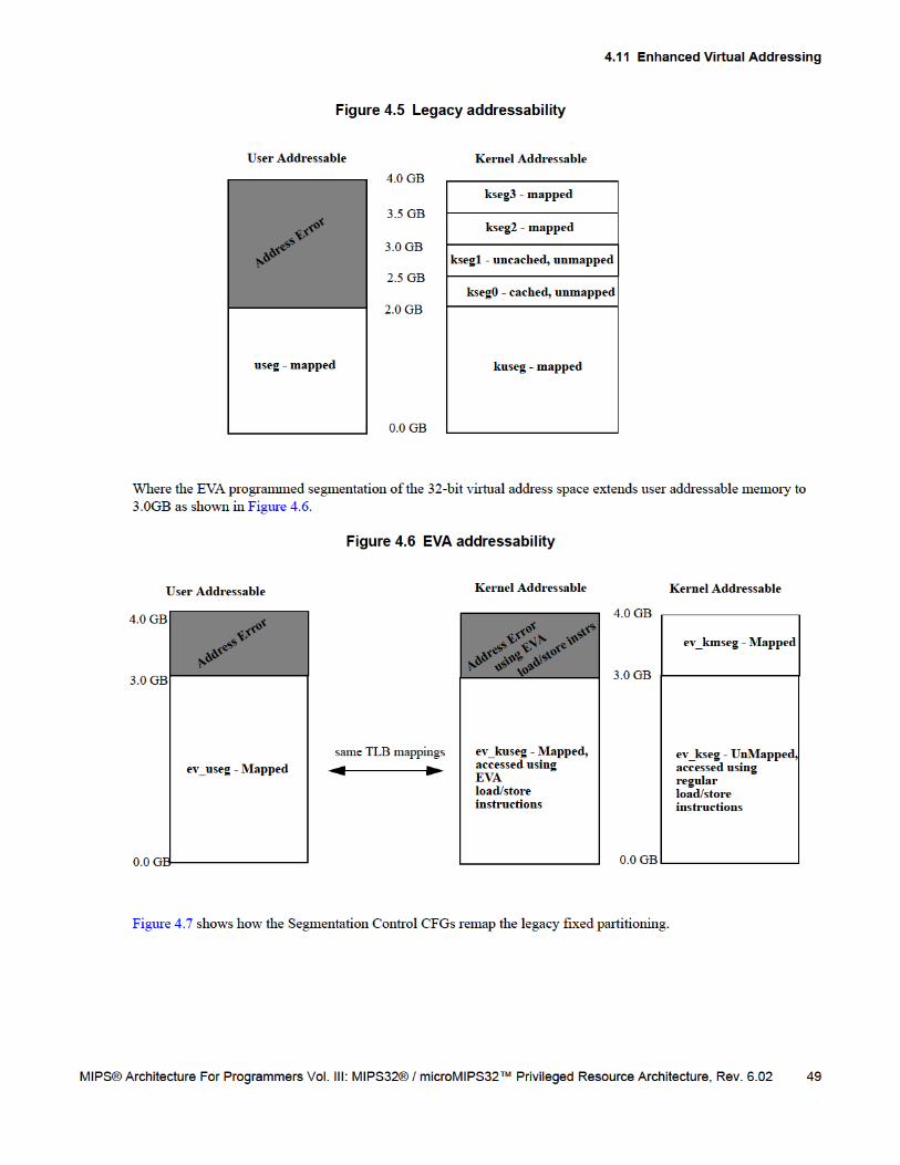
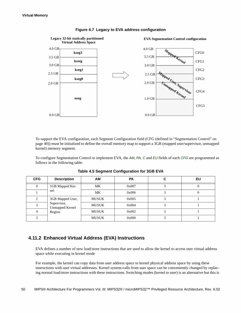
Virtual Memory
50 MIPS® Architecture For Programmers Vol. III: MIPS32® / microMIPS32™ Privileged Resource Architecture, Rev. 6.02
Figure 4.7 Legacy to EVA address configuration
To support the EVA configuration, each Segment Configuration field (CFG (defined in “Segmentation Control” on page 40)) must be initialized to define the overall memory map to support a 3GB (mapped user/supervisor, unmapped kernel) memory segment.
To configure Segmentation Control to implement EVA, the AM, PA, C and EU fields of each CFG are programmed as follows in the following table.
4.11.2 Enhanced Virtual Address (EVA) Instructions
EVA defines a number of new load/store instructions that are used to allow the kernel to access user virtual address space while executing in kernel mode
For example, the kernel can copy data from user address space to kernel physical address space by using these instructions with user virtual addresses. Kernel system-calls from user space can be conveniently changed by replac-ing normal load/store instructions with these instructions. Switching modes (kernel to user) is an alternative but this is
Table 4.5 Segment Configuration for 3GB EVA
CFG Description AM PA C EU
0 1GB Mapped Ker-nel
MK 0x007 3 0
1 MK 0x006 3 0
2 3GB Mapped User, Supervisor, Unmapped Kernel Region
MUSUK 0x005 3 1
3 MUSUK 0x004 3 1
4 MUSUK 0x002 3 1
5 MUSUK 0x000 3 1
kseg3
useg
0.0 GB
2.0 GB
3.0 GB
3.5 GB
4.0 GB
Virtual Address Space
ksseg
kseg1
kseg0
2.5 GB
Legacy 32-bit statically partitioned
CFG0
EVA Segmentation Control configuration
CFG4
CFG2
CFG1
CFG3
CFG5
Mapped Kernel
Mapped User, Supervisor
Unmapped Kernel
4.0 GB
3.5 GB
3.0 GB
2.5 GB
2.0 GB
1.0 GB
0.0 GB
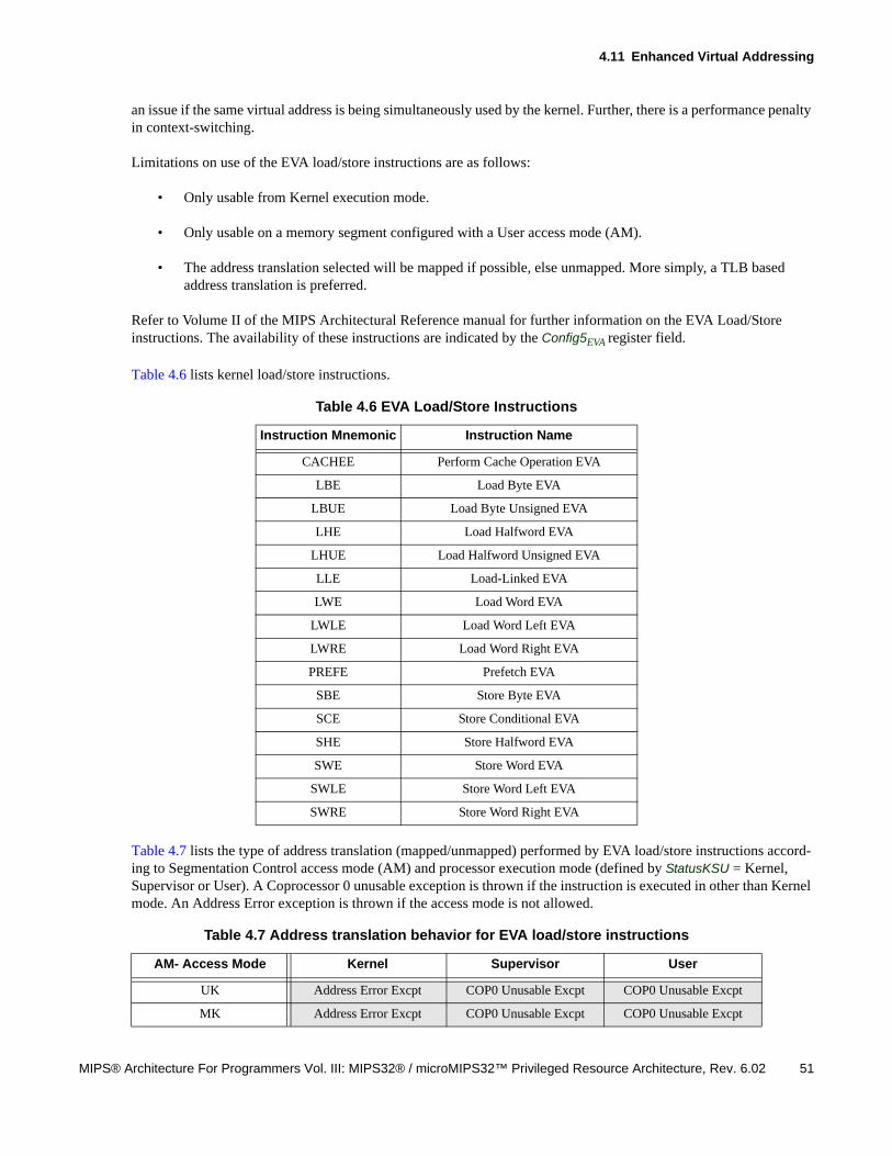
4.11 Enhanced Virtual Addressing
MIPS® Architecture For Programmers Vol. III: MIPS32® / microMIPS32™ Privileged Resource Architecture, Rev. 6.02 51
an issue if the same virtual address is being simultaneously used by the kernel. Further, there is a performance penalty in context-switching.
Limitations on use of the EVA load/store instructions are as follows:
• Only usable from Kernel execution mode.
• Only usable on a memory segment configured with a User access mode (AM).
• The address translation selected will be mapped if possible, else unmapped. More simply, a TLB based address translation is preferred.
Refer to Volume II of the MIPS Architectural Reference manual for further information on the EVA Load/Store instructions. The availability of these instructions are indicated by the Config5EVA register field.
Table 4.6 lists kernel load/store instructions.
Table 4.7 lists the type of address translation (mapped/unmapped) performed by EVA load/store instructions accord-ing to Segmentation Control access mode (AM) and processor execution mode (defined by StatusKSU = Kernel, Supervisor or User). A Coprocessor 0 unusable exception is thrown if the instruction is executed in other than Kernel mode. An Address Error exception is thrown if the access mode is not allowed.
Table 4.6 EVA Load/Store Instructions
Instruction Mnemonic Instruction Name
CACHEE Perform Cache Operation EVA
LBE Load Byte EVA
LBUE Load Byte Unsigned EVA
LHE Load Halfword EVA
LHUE Load Halfword Unsigned EVA
LLE Load-Linked EVA
LWE Load Word EVA
LWLE Load Word Left EVA
LWRE Load Word Right EVA
PREFE Prefetch EVA
SBE Store Byte EVA
SCE Store Conditional EVA
SHE Store Halfword EVA
SWE Store Word EVA
SWLE Store Word Left EVA
SWRE Store Word Right EVA
Table 4.7 Address translation behavior for EVA load/store instructions
AM- Access Mode Kernel Supervisor User
UK Address Error Excpt COP0 Unusable Excpt COP0 Unusable Excpt
MK Address Error Excpt COP0 Unusable Excpt COP0 Unusable Excpt
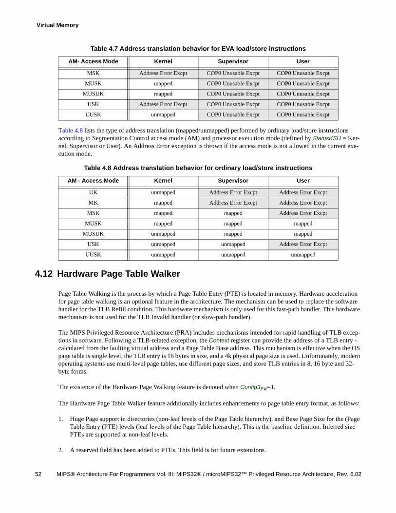
Virtual Memory
52 MIPS® Architecture For Programmers Vol. III: MIPS32® / microMIPS32™ Privileged Resource Architecture, Rev. 6.02
Table 4.8 lists the type of address translation (mapped/unmapped) performed by ordinary load/store instructions according to Segmentation Control access mode (AM) and processor execution mode (defined by StatusKSU = Ker-nel, Supervisor or User). An Address Error exception is thrown if the access mode is not allowed in the current exe-cution mode.
4.12 Hardware Page Table Walker
Page Table Walking is the process by which a Page Table Entry (PTE) is located in memory. Hardware acceleration for page table walking is an optional feature in the architecture. The mechanism can be used to replace the software handler for the TLB Refill condition. This hardware mechanism is only used for this fast-path handler. This hardware mechanism is not used for the TLB Invalid handler (or slow-path handler).
The MIPS Privileged Resource Architecture (PRA) includes mechanisms intended for rapid handling of TLB excep-tions in software. Following a TLB-related exception, the Context register can provide the address of a TLB entry - calculated from the faulting virtual address and a Page Table Base address. This mechanism is effective when the OS page table is single level, the TLB entry is 16 bytes in size, and a 4k physical page size is used. Unfortunately, modern operating systems use multi-level page tables, use different page sizes, and store TLB entries in 8, 16 byte and 32-byte forms.
The existence of the Hardware Page Walking feature is denoted when Config3PW=1.
The Hardware Page Table Walker feature additionally includes enhancements to page table entry format, as follows:
1. Huge Page support in directories (non-leaf levels of the Page Table hierarchy), and Base Page Size for the (Page Table Entry (PTE) levels (leaf levels of the Page Table hierarchy). This is the baseline definition. Inferred size PTEs are supported at non-leaf levels.
2. A reserved field has been added to PTEs. This field is for future extensions.
MSK Address Error Excpt COP0 Unusable Excpt COP0 Unusable Excpt
MUSK mapped COP0 Unusable Excpt COP0 Unusable Excpt
MUSUK mapped COP0 Unusable Excpt COP0 Unusable Excpt
USK Address Error Excpt COP0 Unusable Excpt COP0 Unusable Excpt
UUSK unmapped COP0 Unusable Excpt COP0 Unusable Excpt
Table 4.8 Address translation behavior for ordinary load/store instructions
AM - Access Mode Kernel Supervisor User
UK unmapped Address Error Excpt Address Error Excpt
MK mapped Address Error Excpt Address Error Excpt
MSK mapped mapped Address Error Excpt
MUSK mapped mapped mapped
MUSUK unmapped mapped mapped
USK unmapped unmapped Address Error Excpt
UUSK unmapped unmapped unmapped
Table 4.7 Address translation behavior for EVA load/store instructions
AM- Access Mode Kernel Supervisor User
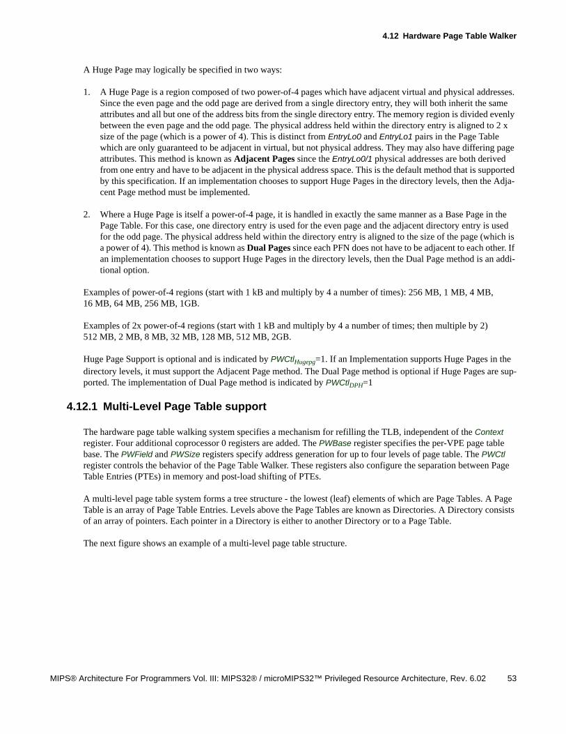
4.12 Hardware Page Table Walker
MIPS® Architecture For Programmers Vol. III: MIPS32® / microMIPS32™ Privileged Resource Architecture, Rev. 6.02 53
A Huge Page may logically be specified in two ways:
1. A Huge Page is a region composed of two power-of-4 pages which have adjacent virtual and physical addresses. Since the even page and the odd page are derived from a single directory entry, they will both inherit the same attributes and all but one of the address bits from the single directory entry. The memory region is divided evenly between the even page and the odd page. The physical address held within the directory entry is aligned to 2 x size of the page (which is a power of 4). This is distinct from EntryLo0 and EntryLo1 pairs in the Page Table which are only guaranteed to be adjacent in virtual, but not physical address. They may also have differing page attributes. This method is known as Adjacent Pages since the EntryLo0/1 physical addresses are both derived from one entry and have to be adjacent in the physical address space. This is the default method that is supported by this specification. If an implementation chooses to support Huge Pages in the directory levels, then the Adja-cent Page method must be implemented.
2. Where a Huge Page is itself a power-of-4 page, it is handled in exactly the same manner as a Base Page in the Page Table. For this case, one directory entry is used for the even page and the adjacent directory entry is used for the odd page. The physical address held within the directory entry is aligned to the size of the page (which is a power of 4). This method is known as Dual Pages since each PFN does not have to be adjacent to each other. If an implementation chooses to support Huge Pages in the directory levels, then the Dual Page method is an addi-tional option.
Examples of power-of-4 regions (start with 1 kB and multiply by 4 a number of times): 256 MB, 1 MB, 4 MB, 16 MB, 64 MB, 256 MB, 1GB.
Examples of 2x power-of-4 regions (start with 1 kB and multiply by 4 a number of times; then multiple by 2) 512 MB, 2 MB, 8 MB, 32 MB, 128 MB, 512 MB, 2GB.
Huge Page Support is optional and is indicated by PWCtlHugepg=1. If an Implementation supports Huge Pages in the directory levels, it must support the Adjacent Page method. The Dual Page method is optional if Huge Pages are sup-ported. The implementation of Dual Page method is indicated by PWCtlDPH=1
4.12.1 Multi-Level Page Table support
The hardware page table walking system specifies a mechanism for refilling the TLB, independent of the Context register. Four additional coprocessor 0 registers are added. The PWBase register specifies the per-VPE page table base. The PWField and PWSize registers specify address generation for up to four levels of page table. The PWCtl register controls the behavior of the Page Table Walker. These registers also configure the separation between Page Table Entries (PTEs) in memory and post-load shifting of PTEs.
A multi-level page table system forms a tree structure - the lowest (leaf) elements of which are Page Tables. A Page Table is an array of Page Table Entries. Levels above the Page Tables are known as Directories. A Directory consists of an array of pointers. Each pointer in a Directory is either to another Directory or to a Page Table.
The next figure shows an example of a multi-level page table structure.
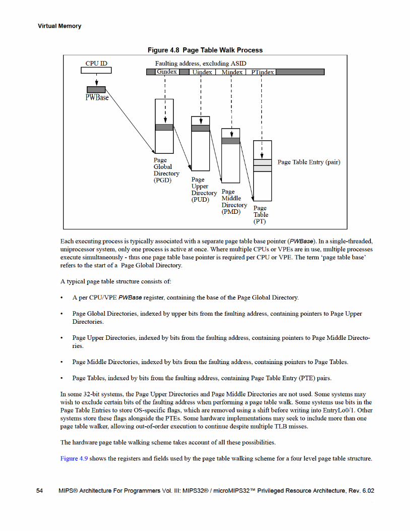
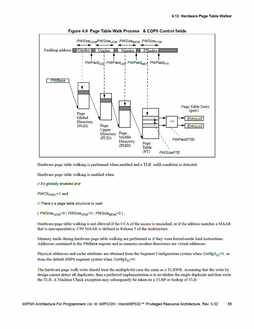
Virtual Memory
56 MIPS® Architecture For Programmers Vol. III: MIPS32® / microMIPS32™ Privileged Resource Architecture, Rev. 6.02
If a synchronous exception condition is detected during the hardware page table walk, the HW walking process is aborted and a TLB Refill exception will be taken. This includes synchronous exceptions such as Address Error, Pre-cise Debug Data Break and other TLB exceptions resulting from accesses to mapped regions.
If an asynchronous exception is detected during the hardware page table walk, the HW walking process is aborted and the asynchronous exception is taken. This includes asynchronous exceptions such as NMI, Cache Error, and Interrupts. It also includes the asynchronous Machine Check exception which results from multiple matching entries being present in the TLB following a TLB write.
Implementations are not required to support hardware page table walk reads from mapped regions of the Virtual Address space. If an implementation does not support reads from mapped regions, an attempted access during a page table walk will cause the process to be aborted, and a TLB Refill exception will be taken.
Pointers within Directories are always treated as 32 bit addresses.
Hardware page table walking is performed as follows:
1. A temporary pointer is loaded with the contents of the PWBase register
2. The native pointer size is set to 4 bytes (32 bits).
3. If the Global Directory is disabled by PWSizeGDW=0, skip to the next step.
• If Huge Pages are supported, check PTEVld bit to determine if entry is PTE. If PTEVld bit is set, write Huge Page into TLB (details left out for brevity, read pseudo-code at end of this section). Page Walking is com-plete after Huge Page is written to TLB.
• Extract PWSizeGDW bits from the faulting address, with least-significant bit PWFieldGDI. This is the Global Directory index (Gindex). Logical OR onto the temporary pointer, after multiplying (shifting) by the native pointer size. The result is a pointer to a location within the Global Directory.
• Perform a memory read from the address in the temporary pointer, of the native pointer size. The returned value is placed into the temporary pointer. If an exception is detected, abort.
4. If the Upper Directory is disabled by PWSizeUDW=0, skip to the next step.
• If Huge Pages are supported, check PTEVld bit to determine if entry is PTE. If PTEVld bit is set, write Huge Page into TLB (details left out for brevity, read pseudo-code at end of this section). Page Walking is com-plete after Huge Page is written to TLB.
• Extract PWSizeUDW bits from the faulting address, with least-significant bit PWFieldUDI. This is the Upper Directory index (Uindex). Logical OR onto the temporary pointer, after multiplying (shifting) by the native pointer size. The result is a pointer to a location within the Upper Directory.
• Perform a memory read from the address in the temporary pointer, of the native pointer size. The returned value is placed into the temporary pointer. If an exception is detected, abort.
5. If the Middle Directory is disabled by PWSizeMDW=0, skip to the next step.
• If Huge Pages are supported, check PTEVld bit to determine if entry is PTE. If PTEVld bit is set, write Huge Page into TLB (details left out for brevity, read pseudo-code at end of this section). Page Walking is com-plete after Huge Page is written to TLB.
4.12 Hardware Page Table Walker
MIPS® Architecture For Programmers Vol. III: MIPS32® / microMIPS32™ Privileged Resource Architecture, Rev. 6.02 57
• Extract PWSizeMDW bits from the faulting address, with least-significant bit PWFieldMDI. This is the Middle Directory index (Mindex). Logical OR onto the temporary pointer, after multiplying (shifting) by the native pointer size. The result is a pointer to a location within the Middle Directory.
• Perform a memory read from the address in the temporary pointer, of the native pointer size. The returned value is placed into the temporary pointer. If an exception is detected, abort.
• The temporary pointer now contains the address of the Page Table to be used.
6. Extract PWSizePTW bits from the faulting address, with least-significant bit PWFieldPTI This is the Page Table
index (PTindex). Multiply (shift) by the native pointer size, then multiply (shift) by the size of the Page Table Entry, specified in PWSizePTEW.
• The temporary pointer now contains the address of the first half of the Page Table Entry.
• Perform a memory read from the address in the temporary pointer, of the native pointer size. The returned value is logically shifted right by PWFieldPTEI bits. This is the first half of the Page Table Entry. If an excep-tion is detected, abort.
7. In the temporary pointer, set the bit located at bit location PWFieldPTEI-1.
• The temporary pointer now contains the address of the second half of the Page Table Entry.
• Perform a memory read from the address in the temporary pointer, of the native pointer size. The returned value is shifted right by PWFieldPTEI bits. This is the second half of the Page Table Entry. If an exception is detected, abort.
8. Write the two halves of the Page Table Entry into the TLB, using the same semantics as the TLBWR (TLB write random) instruction.
9. Continue with program execution.
Coprocessor 0 registers which are used by software on TLB refill exceptions are unused by the hardware page table walking process. The registers and fields used by software are BadVAddr, EntryHi, PageMask, EntryLo0, EntryLo1 and ContextBadVPN2.
4.12.2 PTE and Directory Entry Format
All entries are read from in-memory data structures. There are three types of entries in the baseline definition: Direc-tory Pointer, Huge Page non-leaf PTE of inferred size, and leaf PTE of base size. For options other than baseline, the entry type is a function of the table level and the PTEvld field of an entry. For all but the last level table (leaf level), the PTEvld bit is 0 for directory pointers to the next table and 1 for PTEs. In the leaf table, the entry is always a PTE and the PTEvld bit is not used by Hardware Walker. The PWCtlHugePg register field indicates whether Huge Page
non-leaf PTEs are implemented.
All PTEs are shifted right by PWFieldPTEI -2 (shifting in zeros at the most significant bit) and then rotated right by 2 bits before forming the page-walker equivalents of EntryLo0 and EntryLo1 values. These operations are used to remove the Software-only bits and placing the RI and XI protection bits in the proper bit location before writing the TLB. If the RI and XI bits are implemented and enabled, the HW Page Walker feature requires the RI bit to be placed right of the G bit in the PTE memory format. Similarly, it is required that the XI bit to be placed right of the RI bit in the PTE memory format.
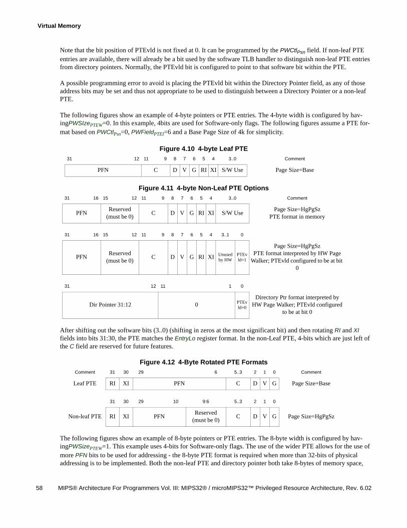
Virtual Memory
58 MIPS® Architecture For Programmers Vol. III: MIPS32® / microMIPS32™ Privileged Resource Architecture, Rev. 6.02
Note that the bit position of PTEvld is not fixed at 0. It can be programmed by the PWCtlPsn field. If non-leaf PTE entries are available, there will already be a bit used by the software TLB handler to distinguish non-leaf PTE entries from directory pointers. Normally, the PTEvld bit is configured to point to that software bit within the PTE.
A possible programming error to avoid is placing the PTEvld bit within the Directory Pointer field, as any of those address bits may be set and thus not appropriate to be used to distinguish between a Directory Pointer or a non-leaf PTE.
The following figures show an example of 4-byte pointers or PTE entries. The 4-byte width is configured by hav-ingPWSIzePTEW=0. In this example, 4bits are used for Software-only flags. The following figures assume a PTE for-mat based on PWCtlPsn=0, PWFieldPTEI=6 and a Base Page Size of 4k for simplicity.
Figure 4.10 4-byte Leaf PTE
Figure 4.11 4-byte Non-Leaf PTE Options
After shifting out the software bits (3..0) (shifting in zeros at the most significant bit) and then rotating RI and XI fields into bits 31:30, the PTE matches the EntryLo register format. In the non-Leaf PTE, 4-bits which are just left of the C field are reserved for future features.
Figure 4.12 4-Byte Rotated PTE Formats
The following figures show an example of 8-byte pointers or PTE entries. The 8-byte width is configured by hav-ingPWSizePTEW=1. This example uses 4-bits for Software-only flags. The use of the wider PTE allows for the use of more PFN bits to be used for addressing - the 8-byte PTE format is required when more than 32-bits of physical addressing is to be implemented. Both the non-leaf PTE and directory pointer both take 8-bytes of memory space,
31 12 11 9 8 7 6 5 4 3..0 Comment
PFN C D V G RI XI S/W Use Page Size=Base
31 16 15 12 11 9 8 7 6 5 4 3..0 Comment
PFNReserved
(must be 0)C D V G RI XI S/W Use
Page Size=HgPgSzPTE format in memory
31 16 15 12 11 9 8 7 6 5 4 3..1 0
PFNReserved
(must be 0)C D V G RI XI Unused
by HWPTEvld=1
Page Size=HgPgSzPTE format interpreted by HW Page
Walker; PTEvld configured to be at bit 0
31 12 11 1 0
Dir Pointer 31:12 0 PTEvld=0
Directory Ptr format interpreted by HW Page Walker; PTEvld configured
to be at bit 0
Comment 31 30 29 6 5..3 2 1 0 Comment
Leaf PTE RI XI PFN C D V G Page Size=Base
31 30 29 10 9:6 5..3 2 1 0
Non-leaf PTE RI XI PFNReserved
(must be 0)C D V G Page Size=HgPgSz
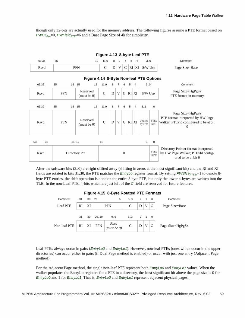
4.12 Hardware Page Table Walker
MIPS® Architecture For Programmers Vol. III: MIPS32® / microMIPS32™ Privileged Resource Architecture, Rev. 6.02 59
though only 32-bits are actually used for the memory address. The following figures assume a PTE format based on PWCtlPsn=0, PWFieldPTEI=6 and a Base Page Size of 4k for simplicity.
Figure 4.13 8-byte Leaf PTE
Figure 4.14 8-Byte Non-leaf PTE Options
After the software bits (3..0) are right shifted away (shifting in zeros at the most significant bit) and the RI and XI fields are rotated to bits 31:30, the PTE matches the EntryLo register format. By setting PWSIzePTEW=1 to denote 8-byte PTE entries, the shift operation is done on the entire 8 byte PTE, but only the lower 4-bytes are written into the TLB. In the non-Leaf PTE, 4-bits which are just left of the C field are reserved for future features.
Figure 4.15 8-Byte Rotated PTE Formats
Leaf PTEs always occur in pairs (EntryLo0 and EntryLo1). However, non-leaf PTEs (ones which occur in the upper directories) can occur either in pairs (if Dual Page method is enabled) or occur with just one entry (Adjacent Page method).
For the Adjacent Page method, the single non-leaf PTE represent both EntryLo0 and EntryLo1 values. When the walker populates the EntryLo registers for a PTE in a directory, the least significant bit above the page size is 0 for EntryLo0 and 1 for EntryLo1. That is, EntryLo0 and EntryLo1 represent adjacent physical pages.
63:36 35 12 11 9 8 7 6 5 4 3..0 Comment
Rsvd PFN C D V G RI XI S/W Use Page Size=Base
63:36 35 16 15 12 11.9 8 7 6 5 4 3..0 Comment
Rsvd PFNReserved
(must be 0)C D V G RI XI S/W Use
Page Size=HgPgSzPTE format in memory
63:39 35 16 15 12 11.9 8 7 6 5 4 3..1 0
Rsvd PFNReserved
(must be 0)C D V G RI XI Unused
by HWPTEvld=1
Page Size=HgPgSzPTE format interpreted by HW Page
Walker; PTEvld configured to be at bit 0
63 32 31..12 11 1 0
Rsvd Directory Ptr 0 PTEvld=0
Directory Pointer format interpreted by HW Page Walker; PTEvld config-
ured to be at bit 0
Comment 31 30 29 6 5..3 2 1 0 Comment
Leaf PTE RI XI PFN C D V G Page Size=Base
31 30 29..10 9..6 5..3 2 1 0
Non-leaf PTE RI XI PFNRsvd
(must be 0)C D V G Page Size=HgPgSz
Virtual Memory
60 MIPS® Architecture For Programmers Vol. III: MIPS32® / microMIPS32™ Privileged Resource Architecture, Rev. 6.02
For the Dual Page method, the two PTEs are read from the directory level by the Hardware Page Walker.
For Huge Page handling, the size of the Huge Page is inferred from the directory level in which the Huge Page resides. For the Adjacent Page Method, the size of each individual PTE in EntryLo0 and EntryLo1 as synthesized from the single Huge Page is always half the inferred size.
If the inferred page size is 2 x power-of-4, then the Adjacent Page Method is used.
If the inferred page size is a power-of-4, then the Dual Page Method is used (if the Dual Page Method is imple-mented). If the Dual Page method is implemented (PWCtlDPH=1), it is implementation-specific whether the PTEVld bit is checked for the second PTE when it is read from memory for writing the second TLB page. The recommended behavior is to check this second PTEVld bit and if it is not set, a Machine Check exception is triggered. The PageGrainMCCause register field is used to differentiate between different types of Machine Check exceptions.
If the inferred Huge Page size is power-of-4, and the Dual Page Methods is not implemented, it is implementation-specific whether a Machine Check is reported.
An example of Huge Page handling follows. It assumes a leaf PTE size of 4 kB.
• PMD Huge Page = 2^9 (PWSizePTW) * 2^12 (PWFieldPTI) = 2^21 = 2 MB. Each EntryLo0/1 page is 1 MB, which is a power-of-4 and use the Adjacent Page method.
• PUD Huge Page = 2^10 (PWSizeMDW) * 2^9 (PWSizePTW) * 2^12 (PWFieldPTI) = 2^31 = 2GB. Each EntryLo0/1 page is 1GB, which is a power-of-4 and would use the Adjacent Page method. Note that the index into PMD has been extended to 10 bits from 9 bits. Each PMD table thus has 1K entries instead of the typical 512 entries.
See also:
• Section 9.18, "PWBase Register (CP0 Register 5, Select 5)" on page 161
• Section 9.19, "PWField Register (CP0 Register 5, Select 6)" on page 161
• Section 9.20, "PWSize Register (CP0 Register 5, Select 7)" on page 164
• Section 9.22, "PWCtl Register (CP0 Register 6, Select 6)" on page 171
4.12.3 Hardware page table walking process
The hardware page table walking process is described in pseudocode as follows:
/* Perform hardware page table walk** Memory accesses are performed using the KERNEL privilege level.* Synchronous exceptions detected on memory accesses cause a silent exit* from page table walking, resulting in a TLB Refill exception.* * Implementations are not required to support page table walk memory * accesses from mapped memory regions. When an unsupported access is* attempted, a silent exit is taken, resulting in a TLB Refill exception.* * Note that if an exception is caused by AddressTranslation or LoadMemory* functions, the exception is not taken, a silent exit is taken, * resulting in a TLB Refill exception.
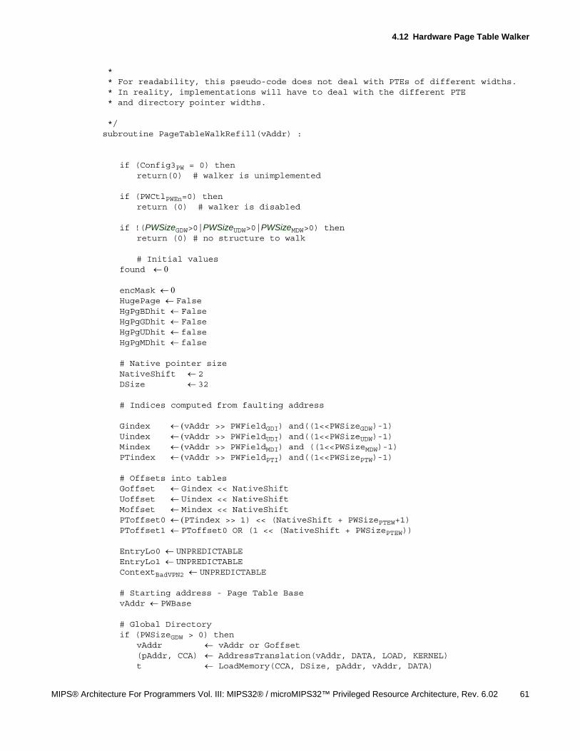
4.12 Hardware Page Table Walker
MIPS® Architecture For Programmers Vol. III: MIPS32® / microMIPS32™ Privileged Resource Architecture, Rev. 6.02 61
* * For readability, this pseudo-code does not deal with PTEs of different widths. * In reality, implementations will have to deal with the different PTE * and directory pointer widths.
*/subroutine PageTableWalkRefill(vAddr) :
if (Config3PW = 0) thenreturn(0) # walker is unimplemented
if (PWCtlPWEn=0) thenreturn (0) # walker is disabled
if !(PWSizeGDW>0|PWSizeUDW>0|PWSizeMDW>0) thenreturn (0) # no structure to walk
# Initial valuesfound
encMask HugePage FalseHgPgBDhit FalseHgPgGDhit FalseHgPgUDhit falseHgPgMDhit false
# Native pointer sizeNativeShift 2DSize 32
# Indices computed from faulting address
Gindex vAddr >> PWFieldGDI) and((1<<PWSizeGDW)-1)Uindex vAddr >> PWFieldUDI) and((1<<PWSizeUDW)-1)Mindex vAddr >> PWFieldMDI) and ((1<<PWSizeMDW)-1)PTindex vAddr >> PWFieldPTI) and((1<<PWSizePTW)-1)
# Offsets into tablesGoffset Gindex << NativeShiftUoffset Uindex << NativeShiftMoffset Mindex << NativeShiftPToffset0 PTindex >> 1) << (NativeShift + PWSizePTEW+1)PToffset1 PToffset0 OR (1 << (NativeShift + PWSizePTEW))
EntryLo0 UNPREDICTABLEEntryLo1 UNPREDICTABLEContextBadVPN2 UNPREDICTABLE
# Starting address - Page Table BasevAddr PWBase
# Global Directoryif (PWSizeGDW > 0) then
vAddr vAddr or Goffset(pAddr, CCA) AddressTranslation(vAddr, DATA, LOAD, KERNEL)t LoadMemory(CCA, DSize, pAddr, vAddr, DATA)
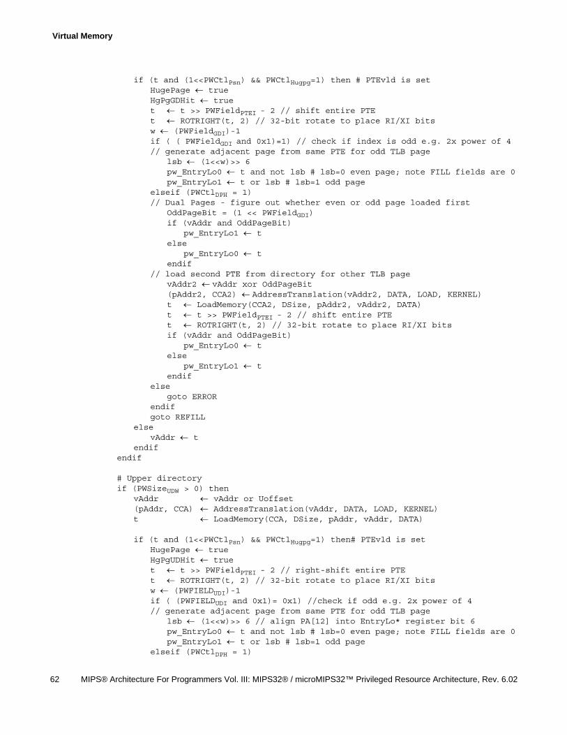
Virtual Memory
62 MIPS® Architecture For Programmers Vol. III: MIPS32® / microMIPS32™ Privileged Resource Architecture, Rev. 6.02
if (t and (1<<PWCtlPsn) && PWCtlHugpg=1) then # PTEvld is setHugePage trueHgPgGDHit truet t >> PWFieldPTEI - 2 // shift entire PTEt ROTRIGHT(t, 2) // 32-bit rotate to place RI/XI bitsw (PWFieldGDI)-1if ( ( PWFieldGDI and 0x1)=1) // check if index is odd e.g. 2x power of 4 // generate adjacent page from same PTE for odd TLB page
lsb (1<<w)>> 6pw_EntryLo0 t and not lsb # lsb=0 even page; note FILL fields are 0pw_EntryLo1 t or lsb # lsb=1 odd page
elseif (PWCtlDPH = 1)// Dual Pages - figure out whether even or odd page loaded first
OddPageBit = (1 << PWFieldGDI)if (vAddr and OddPageBit)
pw_EntryLo1 telse
pw_EntryLo0 tendif
// load second PTE from directory for other TLB pagevAddr2 vAddr xor OddPageBit(pAddr2, CCA2) AddressTranslation(vAddr2, DATA, LOAD, KERNEL)t LoadMemory(CCA2, DSize, pAddr2, vAddr2, DATA)t t >> PWFieldPTEI - 2 // shift entire PTEt ROTRIGHT(t, 2) // 32-bit rotate to place RI/XI bitsif (vAddr and OddPageBit)
pw_EntryLo0 telse
pw_EntryLo1 tendif
elsegoto ERROR
endifgoto REFILL
elsevAddr t
endifendif
# Upper directoryif (PWSizeUDW > 0) then
vAddr vAddr or Uoffset(pAddr, CCA) AddressTranslation(vAddr, DATA, LOAD, KERNEL)t LoadMemory(CCA, DSize, pAddr, vAddr, DATA)
if (t and (1<<PWCtlPsn) && PWCtlHugpg=1) then# PTEvld is setHugePage trueHgPgUDHit truet t >> PWFieldPTEI - 2 // right-shift entire PTEt ROTRIGHT(t, 2) // 32-bit rotate to place RI/XI bitsw (PWFIELDUDI)-1if ( (PWFIELDUDI and 0x1)= 0x1) //check if odd e.g. 2x power of 4 // generate adjacent page from same PTE for odd TLB page
lsb (1<<w)>> 6 // align PA[12] into EntryLo* register bit 6pw_EntryLo0 t and not lsb # lsb=0 even page; note FILL fields are 0pw_EntryLo1 t or lsb # lsb=1 odd page
elseif (PWCtlDPH = 1)
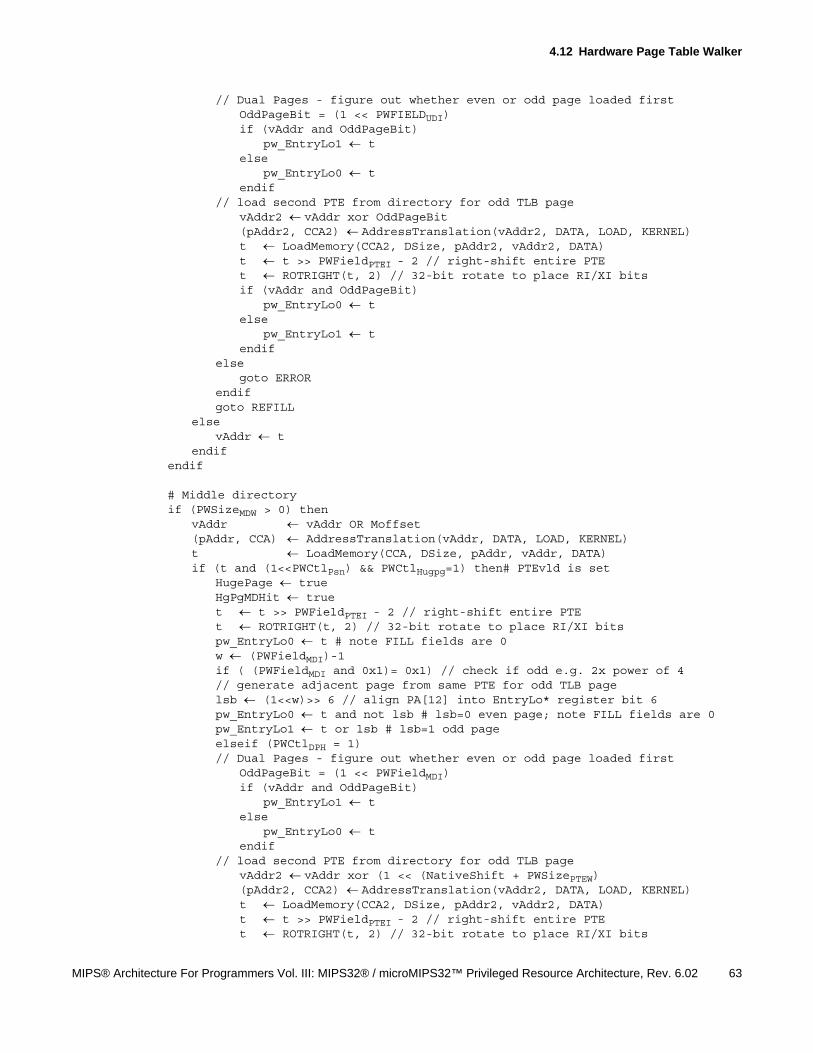
4.12 Hardware Page Table Walker
MIPS® Architecture For Programmers Vol. III: MIPS32® / microMIPS32™ Privileged Resource Architecture, Rev. 6.02 63
// Dual Pages - figure out whether even or odd page loaded firstOddPageBit = (1 << PWFIELDUDI)if (vAddr and OddPageBit)
pw_EntryLo1 telse
pw_EntryLo0 tendif
// load second PTE from directory for odd TLB pagevAddr2 vAddr xor OddPageBit(pAddr2, CCA2) AddressTranslation(vAddr2, DATA, LOAD, KERNEL)t LoadMemory(CCA2, DSize, pAddr2, vAddr2, DATA)t t >> PWFieldPTEI - 2 // right-shift entire PTEt ROTRIGHT(t, 2) // 32-bit rotate to place RI/XI bitsif (vAddr and OddPageBit)
pw_EntryLo0 telse
pw_EntryLo1 tendif
elsegoto ERROR
endifgoto REFILL
elsevAddr t
endifendif
# Middle directoryif (PWSizeMDW > 0) then
vAddr vAddr OR Moffset(pAddr, CCA) AddressTranslation(vAddr, DATA, LOAD, KERNEL)t LoadMemory(CCA, DSize, pAddr, vAddr, DATA)if (t and (1<<PWCtlPsn) && PWCtlHugpg=1) then# PTEvld is set
HugePage trueHgPgMDHit truet t >> PWFieldPTEI - 2 // right-shift entire PTEt ROTRIGHT(t, 2) // 32-bit rotate to place RI/XI bitspw_EntryLo0 t # note FILL fields are 0w (PWFieldMDI)-1if ( (PWFieldMDI and 0x1)= 0x1) // check if odd e.g. 2x power of 4 // generate adjacent page from same PTE for odd TLB pagelsb (1<<w)>> 6 // align PA[12] into EntryLo* register bit 6pw_EntryLo0 t and not lsb # lsb=0 even page; note FILL fields are 0pw_EntryLo1 t or lsb # lsb=1 odd pageelseif (PWCtlDPH = 1)// Dual Pages - figure out whether even or odd page loaded first
OddPageBit = (1 << PWFieldMDI)if (vAddr and OddPageBit)
pw_EntryLo1 telse
pw_EntryLo0 tendif
// load second PTE from directory for odd TLB pagevAddr2 vAddr xor (1 << (NativeShift + PWSizePTEW)(pAddr2, CCA2) AddressTranslation(vAddr2, DATA, LOAD, KERNEL)t LoadMemory(CCA2, DSize, pAddr2, vAddr2, DATA)t t >> PWFieldPTEI - 2 // right-shift entire PTEt ROTRIGHT(t, 2) // 32-bit rotate to place RI/XI bits
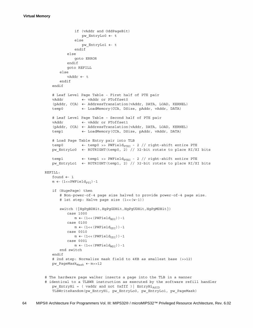
Virtual Memory
64 MIPS® Architecture For Programmers Vol. III: MIPS32® / microMIPS32™ Privileged Resource Architecture, Rev. 6.02
if (vAddr and OddPageBit) pw_EntryLo0 t
elsepw_EntryLo1 t
endifelse
goto ERRORendifgoto REFILL
elsevAddr t
endifendif
# Leaf Level Page Table - First half of PTE pairvAddr vAddr or PToffset0(pAddr, CCA) AddressTranslation(vAddr, DATA, LOAD, KERNEL)temp0 LoadMemory(CCA, DSize, pAddr, vAddr, DATA)
# Leaf Level Page Table - Second half of PTE pairvAddr vAddr or PToffset1(pAddr, CCA) AddressTranslation(vAddr, DATA, LOAD, KERNEL)temp1 LoadMemory(CCA, DSize, pAddr, vAddr, DATA)
# Load Page Table Entry pair into TLBtemp0 temp0 >> PWFieldPTEI - 2 // right-shift entire PTEpw_EntryLo0 ROTRIGHT(temp0, 2) // 32-bit rotate to place RI/XI bits
temp1 temp1 >> PWFieldPTEI - 2 // right-shift entire PTEpw_EntryLo1 ROTRIGHT(temp1, 2) // 32-bit rotate to place RI/XI bits
REFILL:found 1m (1<<PWFieldPTI)-1
if (HugePage) then# Non-power-of-4 page size halved to provide power-of-4 page size.# 1st step: Halve page size (1<<(w-1))
switch ({HgPgBDHit,HgPgGDHit,HgPgUDHit,HgPgMDHit})case 1000
m (1<<(PWFieldBDI))-1case 0100
m (1<<(PWFieldGDI))-1case 0010
m (1<<(PWFieldUDI))-1case 0001
m (1<<(PWFieldMDI))-1end switch
endif# 2nd step: Normalize mask field to 4KB as smallest base (>>12)pw_PageMaskMask m>>12
# The hardware page walker inserts a page into the TLB in a manner# identical to a TLBWR instruction as executed by the software refill handler
pw_EntryHi = ( vaddr and not 0xfff )| EntryHiASIDTLBWriteRandom(pw_EntryHi, pw_EntryLo0, pw_EntryLo1, pw_PageMask)
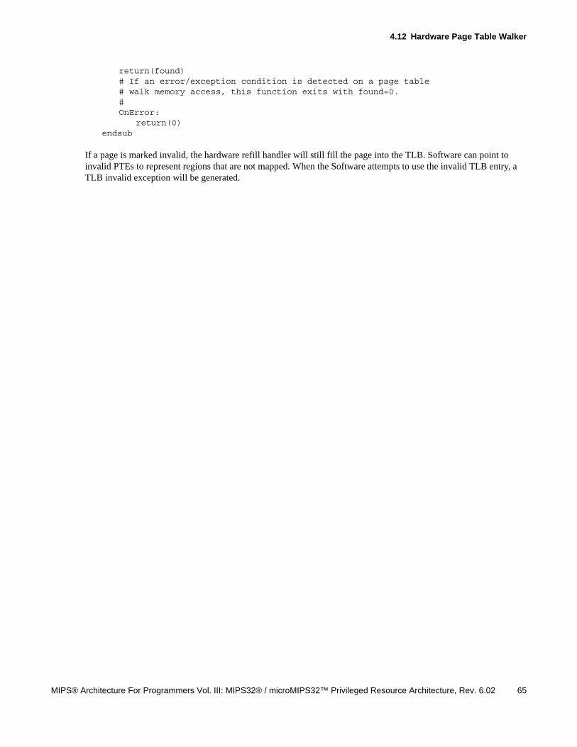
4.12 Hardware Page Table Walker
MIPS® Architecture For Programmers Vol. III: MIPS32® / microMIPS32™ Privileged Resource Architecture, Rev. 6.02 65
return(found)# If an error/exception condition is detected on a page table# walk memory access, this function exits with found=0.#OnError:
return(0)endsub
If a page is marked invalid, the hardware refill handler will still fill the page into the TLB. Software can point to invalid PTEs to represent regions that are not mapped. When the Software attempts to use the invalid TLB entry, a TLB invalid exception will be generated.

Virtual Memory
66 MIPS® Architecture For Programmers Vol. III: MIPS32® / microMIPS32™ Privileged Resource Architecture, Rev. 6.02
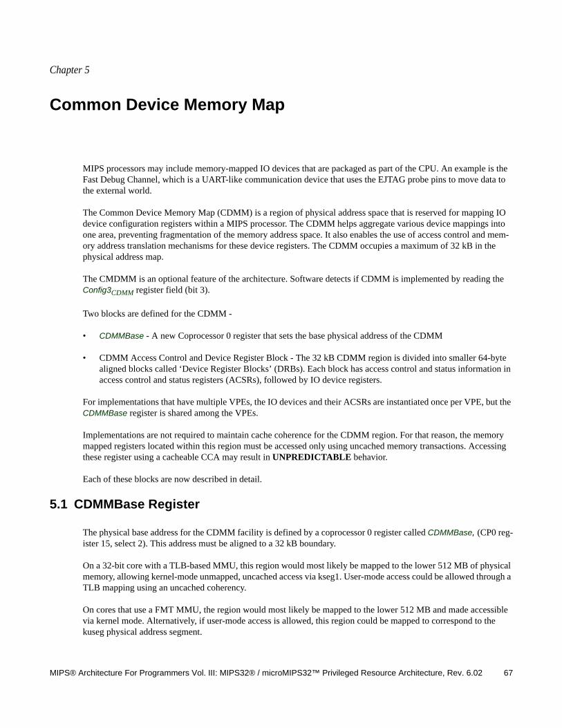
Chapter 5
MIPS® Architecture For Programmers Vol. III: MIPS32® / microMIPS32™ Privileged Resource Architecture, Rev. 6.02 67
Common Device Memory Map
MIPS processors may include memory-mapped IO devices that are packaged as part of the CPU. An example is the Fast Debug Channel, which is a UART-like communication device that uses the EJTAG probe pins to move data to the external world.
The Common Device Memory Map (CDMM) is a region of physical address space that is reserved for mapping IO device configuration registers within a MIPS processor. The CDMM helps aggregate various device mappings into one area, preventing fragmentation of the memory address space. It also enables the use of access control and mem-ory address translation mechanisms for these device registers. The CDMM occupies a maximum of 32 kB in the physical address map.
The CMDMM is an optional feature of the architecture. Software detects if CDMM is implemented by reading the Config3CDMM register field (bit 3).
Two blocks are defined for the CDMM -
• CDMMBase - A new Coprocessor 0 register that sets the base physical address of the CDMM
• CDMM Access Control and Device Register Block - The 32 kB CDMM region is divided into smaller 64-byte aligned blocks called ‘Device Register Blocks’ (DRBs). Each block has access control and status information in access control and status registers (ACSRs), followed by IO device registers.
For implementations that have multiple VPEs, the IO devices and their ACSRs are instantiated once per VPE, but the CDMMBase register is shared among the VPEs.
Implementations are not required to maintain cache coherence for the CDMM region. For that reason, the memory mapped registers located within this region must be accessed only using uncached memory transactions. Accessing these register using a cacheable CCA may result in UNPREDICTABLE behavior.
Each of these blocks are now described in detail.
5.1 CDMMBase Register
The physical base address for the CDMM facility is defined by a coprocessor 0 register called CDMMBase, (CP0 reg-ister 15, select 2). This address must be aligned to a 32 kB boundary.
On a 32-bit core with a TLB-based MMU, this region would most likely be mapped to the lower 512 MB of physical memory, allowing kernel-mode unmapped, uncached access via kseg1. User-mode access could be allowed through a TLB mapping using an uncached coherency.
On cores that use a FMT MMU, the region would most likely be mapped to the lower 512 MB and made accessible via kernel mode. Alternatively, if user-mode access is allowed, this region could be mapped to correspond to the kuseg physical address segment.
Common Device Memory Map
68 MIPS® Architecture For Programmers Vol. III: MIPS32® / microMIPS32™ Privileged Resource Architecture, Rev. 6.02
On cores that use a BAT MMU, if only kernel mode access is allowed, the region would be mapped to a physical address region reachable through kseg1 or kseg2/3 (using uncached coherency). If user mode access is allowed, the useg BAT entry must use an uncached coherency.
Please refer to Section 9.42 on page 227 for the description of the CDMMBase register.
5.2 CDMM - Access Control and Device Register Blocks
The CDMM is divided into 64-byte aligned segments named ‘Device Register Blocks’ (DRBs), Each device occupies at least one DRB. If a device needs additional address space, it can occupy multiple contiguous 64-byte blocks, e.g., multiple DRBs which are adjacent in the physical address map. For each device, device type identification and access control information is located in the DRB allocated for the device with the lowest physical address.
Access control information is specified via ‘Access Control and Status Registers’ (ACSRs) that are found at the start of the DRB allocated for the device with the lowest physical address. The ACSR for a device holds the size of the IO device, and hence also act as a pointer to the start of the next device and its’ ACSR. ACSRs are only accessible in kernel mode. The ACSR is followed by the data/control registers for the IO device. Figure 5.1 shows the organization of the CDMM.
Reading any of the IO device registers in either usermode or supervisor mode when such accesses are not allowed, results in all zeros being returned. Writing any of the IO device registers in either usermode or supervisor mode when such accesses are not allowed, results in the write being ignored and the register not being modified. Reading any of the ACSR registers while not in kernel mode results in all zeros being returned. Writing any of the ACSR registers while not in kernel mode results in the write being ignored and the ACSR not being modified.
Since the ACSR act as a pointer that can only increment, the devices must be allocated in the memory space in a spe-cific manner. The first device must be located at the address pointed by the CDMMBase register and any subsequent device is allocated in the next available adjacent DRB.
If the CI bit is set in the CDMMBASE register, the first DRB of the CDMM (at offset 0x0 from the CDMMBase) is reserved for implementation specific use.
Common Device Memory Map
70 MIPS® Architecture For Programmers Vol. III: MIPS32® / microMIPS32™ Privileged Resource Architecture, Rev. 6.02
DevSize 21:16 This field specifies the number of extra 64-byte blocks allocated to this device. A value of 0 indicates that only one 64-byte block is allocated. This also determines the location of the next device block. A device is limited to 4 kB of memory.
R Preset Required
DevRev 15:12 This field specifies the revision of device. This field is combined with the DevType field to denote the specific device revision.
R Preset Required
Uw 3 This bit indicates if user-mode write access to this device is enabled. A value of 1 indicates that access is enabled. A value of 0 indicates that access is disabled. An attempt to write to the device while in user mode with access dis-abled is ignored.
R/W 0 Required
Ur 2 This bit indicates if user-mode read access to this device is enabled. A value of 1 indicates that access is enabled. A value of 0 indicates that access is disabled. An attempt to read from the device while in user mode with access dis-abled is ignored.
R/W 0 Required
Sw 1 This bit indicates if supervisor-mode write access to this device is enabled. A value of 1 indicates that access is enabled. A value of 0 indicates that access is disabled. An attempt to write to the device while in supervisor mode with access disabled is ignored.
R/W 0 Required
Sr 0 This bit indicates if supervisor-mode read access to this device is enabled. A value of 1 indicates that access is enabled. A value of 0 indicates that access is disabled. An attempt to read from the device while in supervisor mode with access disabled is ignored.
R/W 0 Required
0 63:32, 11:4 Reserved for future use. Ignored on write; returns zero on read.
R 0 Required
Table 5.1 Access Control and Status Register Field Descriptions (Continued)
Fields
DescriptionRead / Write
Reset State ComplianceName Bits
Chapter 6
MIPS® Architecture For Programmers Vol. III: MIPS32® / microMIPS32™ Privileged Resource Architecture, Rev. 6.02 71
Interrupts and Exceptions
Release 2 of the Architecture added the following features related to the processing of Exceptions and Interrupts:
• The addition of the Coprocessor 0 EBase register, which allows the exception vector base address to be modified for exceptions that occur when StatusBEV equals 0. The EBase register is required.
• The extension of the Release 1 interrupt control mechanism to include two optional interrupt modes:
• Vectored Interrupt (VI) mode, in which the various sources of interrupts are prioritized by the processor and each interrupt is vectored directly to a dedicated handler. When combined with GPR shadow registers, intro-duced in the next chapter, this mode significantly reduces the number of cycles required to process an inter-rupt.
• External Interrupt Controller (EIC) mode, in which the definition of the coprocessor 0 register fields associ-ated with interrupts changes to support an external interrupt controller. This can support many more priori-tized interrupts, while still providing the ability to vector an interrupt directly to a dedicated handler and take advantage of the GPR shadow registers.
• The ability to stop the Count register for highly power-sensitive applications in which the Count register is not used, or for reduced power mode. This change is required.
• The addition of the DI and EI instructions which provide the ability to atomically disable or enable interrupts. Both instructions are required.
• The addition of the TI and PCI bits in the Cause register to denote pending timer and performance counter inter-rupts. This change is required.
• The addition of an execution hazard sequence which can be used to clear hazards introduced when software writes to a coprocessor 0 register which affects the interrupt system state.
6.1 Interrupts
Release 1 of the Architecture included support for two software interrupts, six hardware interrupts, and two special-purpose interrupts: timer and performance counter. The timer and performance counter interrupts were combined with hardware interrupt 5 in an implementation-dependent manner. Interrupts were handled either through the general exception vector (offset 0x180) or the special interrupt vector (0x200), based on the value of CauseIV. Software was required to prioritize interrupts as a function of the CauseIP bits in the interrupt handler prologue.
Release 2 of the Architecture adds an upward-compatible extension to the Release 1 interrupt architecture that sup-ports vectored interrupts. In addition, Release 2 adds a new interrupt mode that supports the use of an external inter-rupt controller by changing the interrupt architecture.
Although a Non-Maskable Interrupt (NMI) includes “interrupt” in its name, it is more correctly described as an NMI exception because it does not affect, nor is it controlled by the processor interrupt system.
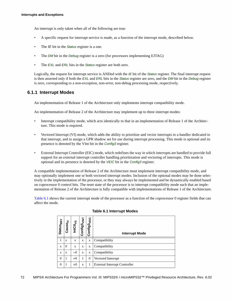
Interrupts and Exceptions
72 MIPS® Architecture For Programmers Vol. III: MIPS32® / microMIPS32™ Privileged Resource Architecture, Rev. 6.02
An interrupt is only taken when all of the following are true:
• A specific request for interrupt service is made, as a function of the interrupt mode, described below.
• The IE bit in the Status register is a one.
• The DM bit in the Debug register is a zero (for processors implementing EJTAG)
• The EXL and ERL bits in the Status register are both zero.
Logically, the request for interrupt service is ANDed with the IE bit of the Status register. The final interrupt request is then asserted only if both the EXL and ERL bits in the Status register are zero, and the DM bit in the Debug register is zero, corresponding to a non-exception, non-error, non-debug processing mode, respectively.
6.1.1 Interrupt Modes
An implementation of Release 1 of the Architecture only implements interrupt compatibility mode.
An implementation of Release 2 of the Architecture may implement up to three interrupt modes:
• Interrupt compatibility mode, which acts identically to that in an implementation of Release 1 of the Architec-ture. This mode is required.
• Vectored Interrupt (VI) mode, which adds the ability to prioritize and vector interrupts to a handler dedicated to that interrupt, and to assign a GPR shadow set for use during interrupt processing. This mode is optional and its presence is denoted by the VInt bit in the Config3 register.
• External Interrupt Controller (EIC) mode, which redefines the way in which interrupts are handled to provide full support for an external interrupt controller handling prioritization and vectoring of interrupts. This mode is optional and its presence is denoted by the VEIC bit in the Config3 register.
A compatible implementation of Release 2 of the Architecture must implement interrupt compatibility mode, and may optionally implement one or both vectored interrupt modes. Inclusion of the optional modes may be done selec-tively in the implementation of the processor, or they may always be implemented and be dynamically enabled based on coprocessor 0 control bits. The reset state of the processor is to interrupt compatibility mode such that an imple-mentation of Release 2 of the Architecture is fully compatible with implementations of Release 1 of the Architecture.
Table 6.1 shows the current interrupt mode of the processor as a function of the coprocessor 0 register fields that can affect the mode.
Table 6.1 Interrupt Modes
Sta
tus B
EV
Cau
se I
V
IntC
tlV
S
Co
nfi
g3 V
INT
Co
nfi
g3 V
EIC
Interrupt Mode
1 x x x x Compatibility
x 0 x x x Compatibility
x x 0 x x Compatibility
0 1 0 1 0 Vectored Interrupt
0 1 0 x 1 External Interrupt Controller
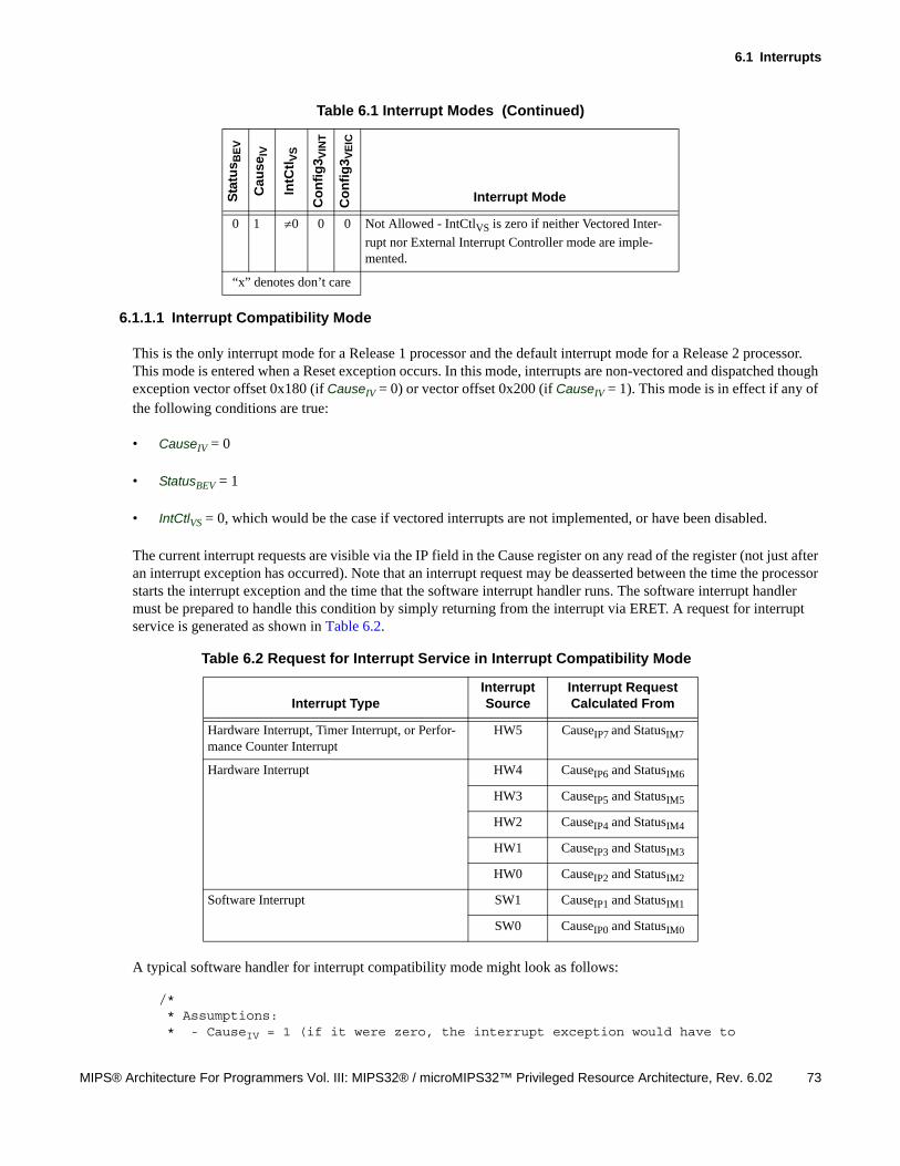
6.1 Interrupts
MIPS® Architecture For Programmers Vol. III: MIPS32® / microMIPS32™ Privileged Resource Architecture, Rev. 6.02 73
6.1.1.1 Interrupt Compatibility Mode
This is the only interrupt mode for a Release 1 processor and the default interrupt mode for a Release 2 processor. This mode is entered when a Reset exception occurs. In this mode, interrupts are non-vectored and dispatched though exception vector offset 0x180 (if CauseIV = 0) or vector offset 0x200 (if CauseIV = 1). This mode is in effect if any of the following conditions are true:
• CauseIV = 0
• StatusBEV = 1
• IntCtlVS = 0, which would be the case if vectored interrupts are not implemented, or have been disabled.
The current interrupt requests are visible via the IP field in the Cause register on any read of the register (not just after an interrupt exception has occurred). Note that an interrupt request may be deasserted between the time the processor starts the interrupt exception and the time that the software interrupt handler runs. The software interrupt handler must be prepared to handle this condition by simply returning from the interrupt via ERET. A request for interrupt service is generated as shown in Table 6.2.
A typical software handler for interrupt compatibility mode might look as follows:
/* * Assumptions: * - CauseIV = 1 (if it were zero, the interrupt exception would have to
0 1 0 0 0 Not Allowed - IntCtlVS is zero if neither Vectored Inter-
rupt nor External Interrupt Controller mode are imple-mented.
“x” denotes don’t care
Table 6.2 Request for Interrupt Service in Interrupt Compatibility Mode
Interrupt TypeInterrupt Source
Interrupt Request Calculated From
Hardware Interrupt, Timer Interrupt, or Perfor-mance Counter Interrupt
HW5 CauseIP7 and StatusIM7
Hardware Interrupt HW4 CauseIP6 and StatusIM6
HW3 CauseIP5 and StatusIM5
HW2 CauseIP4 and StatusIM4
HW1 CauseIP3 and StatusIM3
HW0 CauseIP2 and StatusIM2
Software Interrupt SW1 CauseIP1 and StatusIM1
SW0 CauseIP0 and StatusIM0
Table 6.1 Interrupt Modes (Continued)
Sta
tus B
EV
Ca
use
IV
IntC
tlV
S
Co
nfi
g3 V
INT
Co
nfi
g3
VE
IC
Interrupt Mode
Interrupts and Exceptions
74 MIPS® Architecture For Programmers Vol. III: MIPS32® / microMIPS32™ Privileged Resource Architecture, Rev. 6.02
* be isolated from the general exception vector before getting * here) * - GPRs k0 and k1 are available (no shadow register switches invoked in * compatibility mode) * - The software priority is IP7..IP0 (HW5..HW0, SW1..SW0) * * Location: Offset 0x200 from exception base */
IVexception:mfc0 k0, C0_Cause /* Read Cause register for IP bits */mfc0 k1, C0_Status /* and Status register for IM bits */andi k0, k0, M_CauseIM /* Keep only IP bits from Cause */and k0, k0, k1 /* and mask with IM bits */beq k0, zero, Dismiss /* no bits set - spurious interrupt */clz k0, k0 /* Find first bit set, IP7..IP0; k0 = 16..23 */xori k0, k0, 0x17 /* 16..23 => 7..0 */sll k0, k0, VS /* Shift to emulate software IntCtlVS */la k1, VectorBase /* Get base of 8 interrupt vectors */addu k0, k0, k1 /* Compute target from base and offset */jr k0 /* Jump to specific exception routine */nop
/* * Each interrupt processing routine processes a specific interrupt, analogous * to those reached in VI or EIC interrupt mode. Since each processing routine * is dedicated to a particular interrupt line, it has the context to know * which line was asserted. Each processing routine may need to look further * to determine the actual source of the interrupt if multiple interrupt requests * are ORed together on a single IP line. Once that task is performed, the * interrupt may be processed in one of two ways: * * - Completely at interrupt level (e.g., a simply UART interrupt). The * SimpleInterrupt routine below is an example of this type. * - By saving sufficient state and re-enabling other interrupts. In this * case the software model determines which interrupts are disabled during * the processing of this interrupt. Typically, this is either the single * StatusIM bit that corresponds to the interrupt being processed, or some * collection of other StatusIM bits so that “lower” priority interrupts are * also disabled. The NestedInterrupt routine below is an example of this type. */
SimpleInterrupt:/* * Process the device interrupt here and clear the interupt request * at the device. In order to do this, some registers may need to be * saved and restored. The coprocessor 0 state is such that an ERET * will simply return to the interrupted code. */
eret /* Return to interrupted code */
NestedException:/* * Nested exceptions typically require saving the EPC and Status registers, * any GPRs that may be modified by the nested exception routine, disabling * the appropriate IM bits in Status to prevent an interrupt loop, putting * the processor in kernel mode, and re-enabling interrupts. The sample code * below cannot cover all nuances of this processing and is intended only
6.1 Interrupts
MIPS® Architecture For Programmers Vol. III: MIPS32® / microMIPS32™ Privileged Resource Architecture, Rev. 6.02 75
* to demonstrate the concepts. */
/* Save GPRs here, and setup software context */mfc0 k0, C0_EPC /* Get restart address */sw k0, EPCSave /* Save in memory */mfc0 k0, C0_Status /* Get Status value */sw k0, StatusSave /* Save in memory */li k1, ~IMbitsToClear /* Get Im bits to clear for this interrupt */
/* this must include at least the IM bit *//* for the current interrupt, and may include *//* others */
and k0, k0, k1 /* Clear bits in copy of Status */ins k0, zero, S_StatusEXL, (W_StatusKSU+W_StatusERL+W_StatusEXL)
/* Clear KSU, ERL, EXL bits in k0 */mtc0 k0, C0_Status /* Modify mask, switch to kernel mode, */
/* re-enable interrupts */
/* * Process interrupt here, including clearing device interrupt. * In some environments this may be done with a thread running in * kernel or user mode. Such an environment is well beyond the scope of * this example. */
/* * To complete interrupt processing, the saved values must be restored * and the original interrupted code restarted. */
di /* Disable interrupts - may not be required */lw k0, StatusSave /* Get saved Status (including EXL set) */lw k1, EPCSave /* and EPC */mtc0 k0, C0_Status /* Restore the original value */mtc0 k1, C0_EPC /* and EPC *//* Restore GPRs and software state */eret /* Dismiss the interrupt */
6.1.1.2 Vectored Interrupt Mode
Vectored Interrupt mode builds on the interrupt compatibility mode by adding a priority encoder to prioritize pending interrupts and to generate a vector with which each interrupt can be directed to a dedicated handler routine. This mode also allows each interrupt to be mapped to a GPR shadow set for use by the interrupt handler. Vectored Inter-rupt mode is in effect if all of the following conditions are true:
• Config3VInt = 1
• Config3VEIC = 0
• IntCtlVS 0
• CauseIV = 1
• StatusBEV = 0
Interrupts and Exceptions
76 MIPS® Architecture For Programmers Vol. III: MIPS32® / microMIPS32™ Privileged Resource Architecture, Rev. 6.02
In VI interrupt mode, the six hardware interrupts are interpreted as individual hardware interrupt requests. The timer and performance counter interrupts are combined in an implementation-dependent way with the hardware interrupts (with the interrupt with which they are combined indicated by IntCtlIPTI and IntCtlIPPCI, respectively) to provide the
appropriate relative priority of these interrupts with that of the hardware interrupts. The processor interrupt logic ANDs each of the CauseIP bits with the corresponding StatusIM bits. If any of these values is 1, and if interrupts are
enabled (StatusIE = 1, StatusEXL = 0, and StatusERL = 0), an interrupt is signaled and a priority encoder scans the val-
ues in the order shown in Table 6.3.
The priority order places a relative priority on each hardware interrupt and places the software interrupts at a priority lower than all hardware interrupts. When the priority encoder finds the highest priority pending interrupt, it outputs an encoded vector number that is used in the calculation of the handler for that interrupt, as described below. This is shown pictorially in Figure 6.1.
Table 6.3 Relative Interrupt Priority for Vectored Interrupt Mode
Relative Priority
Interrupt Type
Interrupt Source
Interrupt Request Calculated From
Vector Number Generated by
Priority Encoder
Highest Priority Hardware HW5 CauseIP7 and StatusIM7 7
HW4 CauseIP6 and StatusIM6 6
HW3 CauseIP5 and StatusIM5 5
HW2 CauseIP4 and StatusIM4 4
HW1 CauseIP3 and StatusIM3 3
HW0 CauseIP2 and StatusIM2 2
Software SW1 CauseIP1 and StatusIM1 1
Lowest Priority SW0 CauseIP0 and StatusIM0 0
Interrupts and Exceptions
78 MIPS® Architecture For Programmers Vol. III: MIPS32® / microMIPS32™ Privileged Resource Architecture, Rev. 6.02
sw k0, StatusSave /* Save in memory */mfc0 k0, C0_SRSCtl /* Save SRSCtl if changing shadow sets */sw k0, SRSCtlSaveli k1, ~IMbitsToClear /* Get Im bits to clear for this interrupt */
/* this must include at least the IM bit *//* for the current interrupt, and may include *//* others */
and k0, k0, k1 /* Clear bits in copy of Status *//* If switching shadow sets, write new value to SRSCtlPSS here */ins k0, zero, S_StatusEXL, (W_StatusKSU+W_StatusERL+W_StatusEXL)
/* Clear KSU, ERL, EXL bits in k0 */mtc0 k0, C0_Status /* Modify mask, switch to kernel mode, */
/* re-enable interrupts *//* * If switching shadow sets, clear only KSU above, write target * address to EPC, and do execute an eret to clear EXL, switch * shadow sets, and jump to routine */
/* Process interrupt here, including clearing device interrupt */
/* * To complete interrupt processing, the saved values must be restored * and the original interrupted code restarted. */
di /* Disable interrupts - may not be required */lw k0, StatusSave /* Get saved Status (including EXL set) */lw k1, EPCSave /* and EPC */mtc0 k0, C0_Status /* Restore the original value */lw k0, SRSCtlSave /* Get saved SRSCtl */mtc0 k1, C0_EPC /* and EPC */mtc0 k0, C0_SRSCtl /* Restore shadow sets */ehb /* Clear hazard */eret /* Dismiss the interrupt */
6.1.1.3 External Interrupt Controller Mode
External Interrupt Controller Mode redefines the way that the processor interrupt logic is configured to provide sup-port for an external interrupt controller. The interrupt controller is responsible for prioritizing all interrupts, including hardware, software, timer, and performance counter interrupts, and directly supplying to the processor the vector number (and optionally the priority level) of the highest priority interrupt. EIC interrupt mode is in effect if all of the following conditions are true:
• Config3VEIC = 1
• IntCtlVS 0
• CauseIV = 1
• StatusBEV = 0
In EIC interrupt mode, the processor sends the state of the software interrupt requests (CauseIP1..IP0), the timer inter-rupt request (CauseTI), and the performance counter interrupt request (CausePCI) to the external interrupt controller,
where it prioritizes these interrupts in a system-dependent way with other hardware interrupts. The interrupt control-
6.1 Interrupts
MIPS® Architecture For Programmers Vol. III: MIPS32® / microMIPS32™ Privileged Resource Architecture, Rev. 6.02 79
ler can be a hard-wired logic block, or it can be configurable based on control and status registers. This allows the interrupt controller to be more specific or more general as a function of the system environment and needs.
The external interrupt controller prioritizes its interrupt requests and produces the priority level and the vector num-ber of the highest priority interrupt to be serviced. The priority level, called the Requested Interrupt Priority Level (RIPL), is a 6-bit encoded value in the range 0..63, inclusive. A value of 0 indicates that no interrupt requests are pending. The values 1..63 represent the lowest (1) to highest (63) RIPL for the interrupt to be serviced. The interrupt controller passes this value on the 6 hardware interrupt lines, which are treated as an encoded value in EIC interrupt mode. There are several implementation options available for the vector offset:
1. The first option is to treat the RIPL value as the vector number for the processor.
2. The second option is to send a separate vector number along with the RIPL to the processor.
3. A third option is to send an entire vector offset along with the RIPL to the processor.
StatusIPL (which overlays StatusIM7..IM2) is interpreted as the Interrupt Priority Level (IPL) at which the processor is currently operating (with a value of zero indicating that no interrupt is currently being serviced). When the interrupt controller requests service for an interrupt, the processor compares RIPL with StatusIPL to determine if the requested interrupt has higher priority than the current IPL. If RIPL is strictly greater than StatusIPL, and interrupts are enabled (StatusIE = 1, StatusEXL = 0, and StatusERL = 0) an interrupt request is signaled to the pipeline. When the processor
starts the interrupt exception, it loads RIPL into CauseRIPL (which overlays CauseIP7..IP2) and signals the external interrupt controller to notify it that the request is being serviced. Because CauseRIPL is only loaded by the processor when an interrupt exception is signaled, it is available to software during interrupt processing. The vector number that the EIC passes into the core is combined with the IntCtlVS to determine where the interrupt service routines is located. The vector number is not stored in any software visible register. Some implementations may choose to use the RIPL as the vector number, but this is not a requirement.
In EIC interrupt mode, the external interrupt controller is also responsible for supplying the GPR shadow set number to use when servicing the interrupt. As such, the SRSMap register is not used in this mode, and the mapping of the vectored interrupt to a GPR shadow set is done by programming (or designing) the interrupt controller to provide the correct GPR shadow set number when an interrupt is requested. When the processor loads an interrupt request into CauseRIPL, it also loads the GPR shadow set number into SRSCtlEICSS, which is copied to SRSCtlCSS when the inter-rupt is serviced.
The operation of EIC interrupt mode is shown pictorially in Figure 6.2.
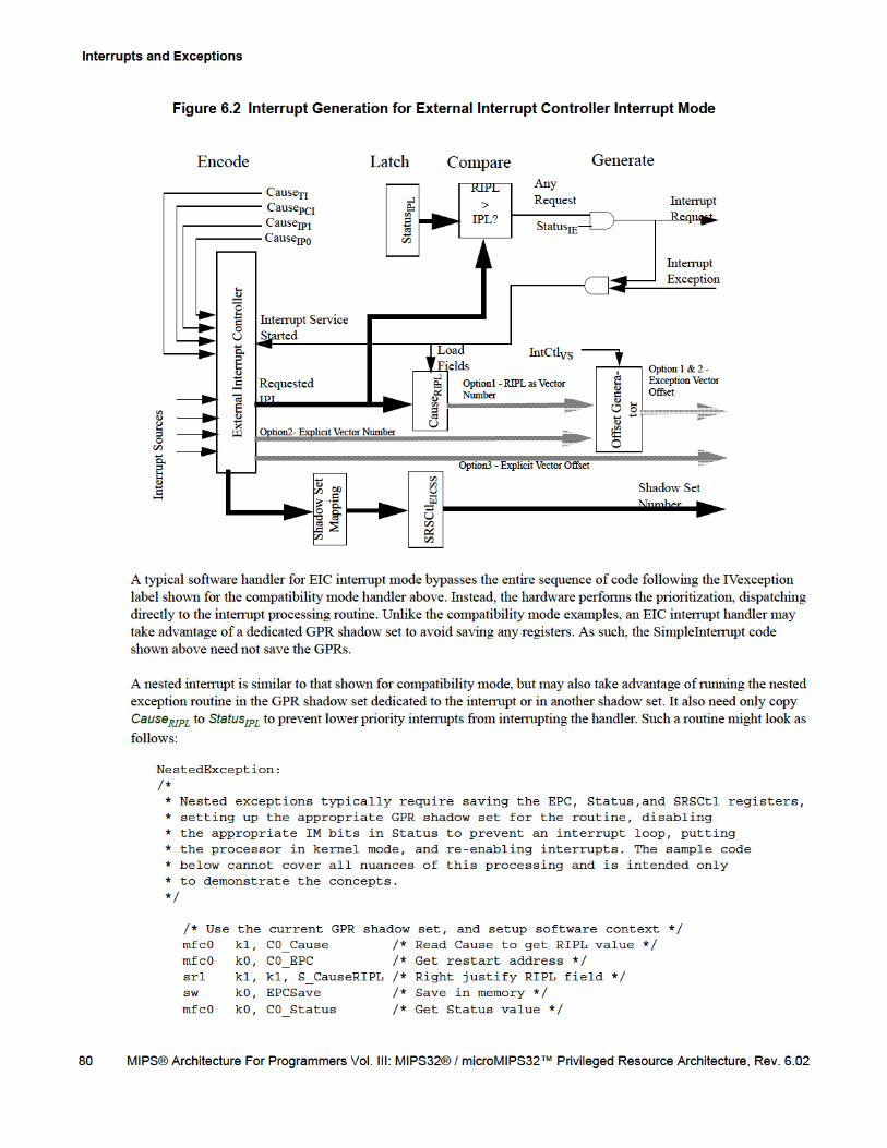
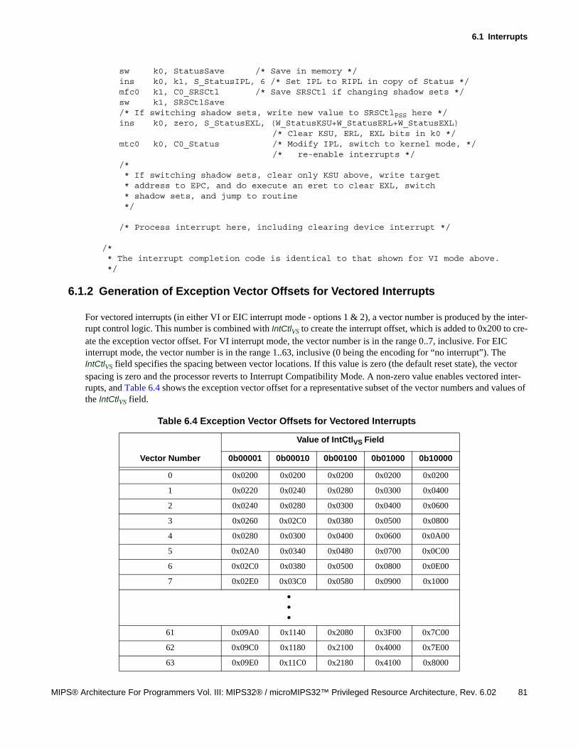
6.1 Interrupts
MIPS® Architecture For Programmers Vol. III: MIPS32® / microMIPS32™ Privileged Resource Architecture, Rev. 6.02 81
sw k0, StatusSave /* Save in memory */ins k0, k1, S_StatusIPL, 6 /* Set IPL to RIPL in copy of Status */mfc0 k1, C0_SRSCtl /* Save SRSCtl if changing shadow sets */sw k1, SRSCtlSave/* If switching shadow sets, write new value to SRSCtlPSS here */ins k0, zero, S_StatusEXL, (W_StatusKSU+W_StatusERL+W_StatusEXL)
/* Clear KSU, ERL, EXL bits in k0 */mtc0 k0, C0_Status /* Modify IPL, switch to kernel mode, */
/* re-enable interrupts *//* * If switching shadow sets, clear only KSU above, write target * address to EPC, and do execute an eret to clear EXL, switch * shadow sets, and jump to routine */
/* Process interrupt here, including clearing device interrupt */
/* * The interrupt completion code is identical to that shown for VI mode above. */
6.1.2 Generation of Exception Vector Offsets for Vectored Interrupts
For vectored interrupts (in either VI or EIC interrupt mode - options 1 & 2), a vector number is produced by the inter-rupt control logic. This number is combined with IntCtlVS to create the interrupt offset, which is added to 0x200 to cre-ate the exception vector offset. For VI interrupt mode, the vector number is in the range 0..7, inclusive. For EIC interrupt mode, the vector number is in the range 1..63, inclusive (0 being the encoding for “no interrupt”). The IntCtlVS field specifies the spacing between vector locations. If this value is zero (the default reset state), the vector spacing is zero and the processor reverts to Interrupt Compatibility Mode. A non-zero value enables vectored inter-rupts, and Table 6.4 shows the exception vector offset for a representative subset of the vector numbers and values of the IntCtlVS field.
Table 6.4 Exception Vector Offsets for Vectored Interrupts
Vector Number
Value of IntCtlVS Field
0b00001 0b00010 0b00100 0b01000 0b10000
0 0x0200 0x0200 0x0200 0x0200 0x0200
1 0x0220 0x0240 0x0280 0x0300 0x0400
2 0x0240 0x0280 0x0300 0x0400 0x0600
3 0x0260 0x02C0 0x0380 0x0500 0x0800
4 0x0280 0x0300 0x0400 0x0600 0x0A00
5 0x02A0 0x0340 0x0480 0x0700 0x0C00
6 0x02C0 0x0380 0x0500 0x0800 0x0E00
7 0x02E0 0x03C0 0x0580 0x0900 0x1000
61 0x09A0 0x1140 0x2080 0x3F00 0x7C00
62 0x09C0 0x1180 0x2100 0x4000 0x7E00
63 0x09E0 0x11C0 0x2180 0x4100 0x8000
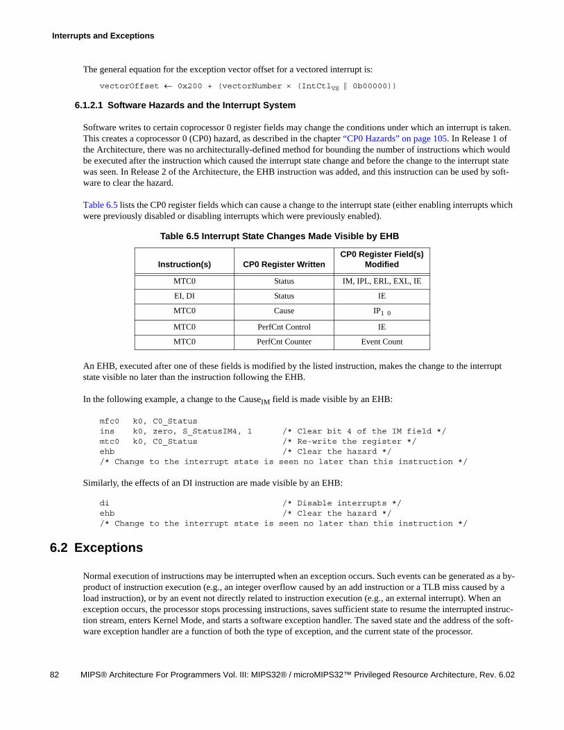
Interrupts and Exceptions
82 MIPS® Architecture For Programmers Vol. III: MIPS32® / microMIPS32™ Privileged Resource Architecture, Rev. 6.02
The general equation for the exception vector offset for a vectored interrupt is:
vectorOffset 0x200 + (vectorNumber (IntCtlVS 0b00000))
6.1.2.1 Software Hazards and the Interrupt System
Software writes to certain coprocessor 0 register fields may change the conditions under which an interrupt is taken. This creates a coprocessor 0 (CP0) hazard, as described in the chapter “CP0 Hazards” on page 105. In Release 1 of the Architecture, there was no architecturally-defined method for bounding the number of instructions which would be executed after the instruction which caused the interrupt state change and before the change to the interrupt state was seen. In Release 2 of the Architecture, the EHB instruction was added, and this instruction can be used by soft-ware to clear the hazard.
Table 6.5 lists the CP0 register fields which can cause a change to the interrupt state (either enabling interrupts which were previously disabled or disabling interrupts which were previously enabled).
An EHB, executed after one of these fields is modified by the listed instruction, makes the change to the interrupt state visible no later than the instruction following the EHB.
In the following example, a change to the CauseIM field is made visible by an EHB:
mfc0 k0, C0_Statusins k0, zero, S_StatusIM4, 1 /* Clear bit 4 of the IM field */mtc0 k0, C0_Status /* Re-write the register */ehb /* Clear the hazard *//* Change to the interrupt state is seen no later than this instruction */
Similarly, the effects of an DI instruction are made visible by an EHB:
di /* Disable interrupts */ehb /* Clear the hazard *//* Change to the interrupt state is seen no later than this instruction */
6.2 Exceptions
Normal execution of instructions may be interrupted when an exception occurs. Such events can be generated as a by-product of instruction execution (e.g., an integer overflow caused by an add instruction or a TLB miss caused by a load instruction), or by an event not directly related to instruction execution (e.g., an external interrupt). When an exception occurs, the processor stops processing instructions, saves sufficient state to resume the interrupted instruc-tion stream, enters Kernel Mode, and starts a software exception handler. The saved state and the address of the soft-ware exception handler are a function of both the type of exception, and the current state of the processor.
Table 6.5 Interrupt State Changes Made Visible by EHB
Instruction(s) CP0 Register WrittenCP0 Register Field(s)
Modified
MTC0 Status IM, IPL, ERL, EXL, IE
EI, DI Status IE
MTC0 Cause IP1 0
MTC0 PerfCnt Control IE
MTC0 PerfCnt Counter Event Count
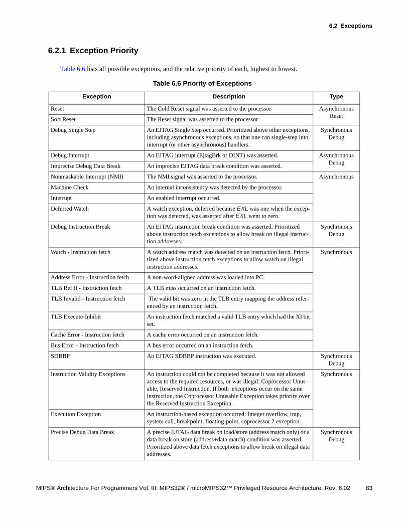
6.2 Exceptions
MIPS® Architecture For Programmers Vol. III: MIPS32® / microMIPS32™ Privileged Resource Architecture, Rev. 6.02 83
6.2.1 Exception Priority
Table 6.6 lists all possible exceptions, and the relative priority of each, highest to lowest.
Table 6.6 Priority of Exceptions
Exception Description Type
Reset The Cold Reset signal was asserted to the processor Asynchronous ResetSoft Reset The Reset signal was asserted to the processor
Debug Single Step An EJTAG Single Step occurred. Prioritized above other exceptions, including asynchronous exceptions, so that one can single-step into interrupt (or other asynchronous) handlers.
Synchronous Debug
Debug Interrupt An EJTAG interrupt (EjtagBrk or DINT) was asserted. Asynchronous DebugImprecise Debug Data Break An imprecise EJTAG data break condition was asserted.
Nonmaskable Interrupt (NMI) The NMI signal was asserted to the processor. Asynchronous
Machine Check An internal inconsistency was detected by the processor.
Interrupt An enabled interrupt occurred.
Deferred Watch A watch exception, deferred because EXL was one when the excep-tion was detected, was asserted after EXL went to zero.
Debug Instruction Break An EJTAG instruction break condition was asserted. Prioritized above instruction fetch exceptions to allow break on illegal instruc-tion addresses.
Synchronous Debug
Watch - Instruction fetch A watch address match was detected on an instruction fetch. Priori-tized above instruction fetch exceptions to allow watch on illegal instruction addresses.
Synchronous
Address Error - Instruction fetch A non-word-aligned address was loaded into PC.
TLB Refill - Instruction fetch A TLB miss occurred on an instruction fetch.
TLB Invalid - Instruction fetch The valid bit was zero in the TLB entry mapping the address refer-enced by an instruction fetch.
TLB Execute-Inhibit An instruction fetch matched a valid TLB entry which had the XI bit set.
Cache Error - Instruction fetch A cache error occurred on an instruction fetch.
Bus Error - Instruction fetch A bus error occurred on an instruction fetch.
SDBBP An EJTAG SDBBP instruction was executed. Synchronous Debug
Instruction Validity Exceptions An instruction could not be completed because it was not allowed access to the required resources, or was illegal: Coprocessor Unus-able, Reserved Instruction. If both exceptions occur on the same instruction, the Coprocessor Unusable Exception takes priority over the Reserved Instruction Exception.
Synchronous
Execution Exception An instruction-based exception occurred: Integer overflow, trap, system call, breakpoint, floating-point, coprocessor 2 exception.
Precise Debug Data Break A precise EJTAG data break on load/store (address match only) or a data break on store (address+data match) condition was asserted. Prioritized above data fetch exceptions to allow break on illegal data addresses.
Synchronous Debug
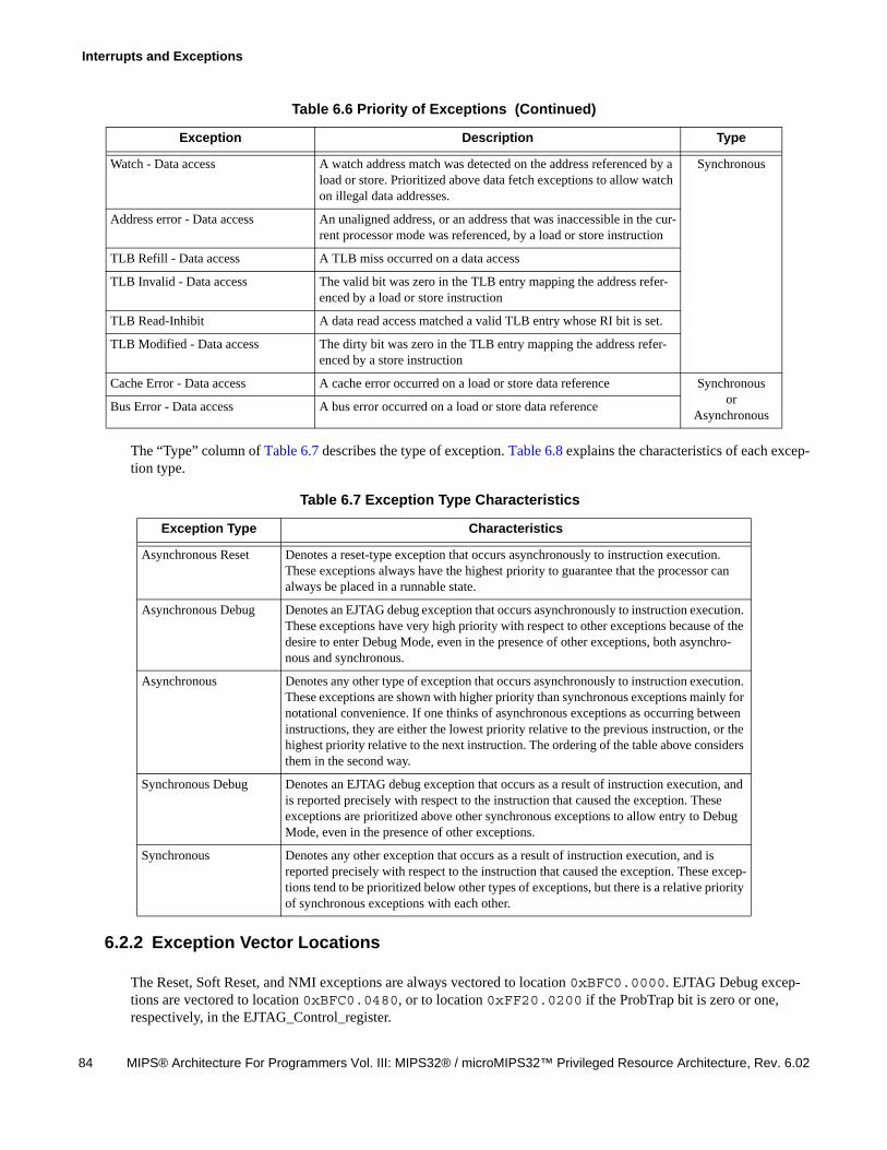
Interrupts and Exceptions
84 MIPS® Architecture For Programmers Vol. III: MIPS32® / microMIPS32™ Privileged Resource Architecture, Rev. 6.02
The “Type” column of Table 6.7 describes the type of exception. Table 6.8 explains the characteristics of each excep-tion type.
6.2.2 Exception Vector Locations
The Reset, Soft Reset, and NMI exceptions are always vectored to location 0xBFC0.0000. EJTAG Debug excep-tions are vectored to location 0xBFC0.0480, or to location 0xFF20.0200 if the ProbTrap bit is zero or one, respectively, in the EJTAG_Control_register.
Watch - Data access A watch address match was detected on the address referenced by a load or store. Prioritized above data fetch exceptions to allow watch on illegal data addresses.
Synchronous
Address error - Data access An unaligned address, or an address that was inaccessible in the cur-rent processor mode was referenced, by a load or store instruction
TLB Refill - Data access A TLB miss occurred on a data access
TLB Invalid - Data access The valid bit was zero in the TLB entry mapping the address refer-enced by a load or store instruction
TLB Read-Inhibit A data read access matched a valid TLB entry whose RI bit is set.
TLB Modified - Data access The dirty bit was zero in the TLB entry mapping the address refer-enced by a store instruction
Cache Error - Data access A cache error occurred on a load or store data reference Synchronousor
AsynchronousBus Error - Data access A bus error occurred on a load or store data reference
Table 6.7 Exception Type Characteristics
Exception Type Characteristics
Asynchronous Reset Denotes a reset-type exception that occurs asynchronously to instruction execution. These exceptions always have the highest priority to guarantee that the processor can always be placed in a runnable state.
Asynchronous Debug Denotes an EJTAG debug exception that occurs asynchronously to instruction execution. These exceptions have very high priority with respect to other exceptions because of the desire to enter Debug Mode, even in the presence of other exceptions, both asynchro-nous and synchronous.
Asynchronous Denotes any other type of exception that occurs asynchronously to instruction execution. These exceptions are shown with higher priority than synchronous exceptions mainly for notational convenience. If one thinks of asynchronous exceptions as occurring between instructions, they are either the lowest priority relative to the previous instruction, or the highest priority relative to the next instruction. The ordering of the table above considers them in the second way.
Synchronous Debug Denotes an EJTAG debug exception that occurs as a result of instruction execution, and is reported precisely with respect to the instruction that caused the exception. These exceptions are prioritized above other synchronous exceptions to allow entry to Debug Mode, even in the presence of other exceptions.
Synchronous Denotes any other exception that occurs as a result of instruction execution, and is reported precisely with respect to the instruction that caused the exception. These excep-tions tend to be prioritized below other types of exceptions, but there is a relative priority of synchronous exceptions with each other.
Table 6.6 Priority of Exceptions (Continued)
Exception Description Type
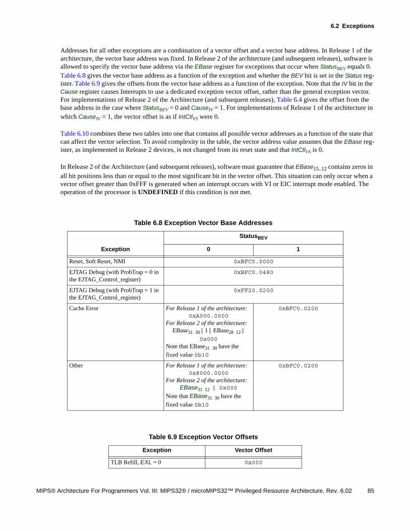
6.2 Exceptions
MIPS® Architecture For Programmers Vol. III: MIPS32® / microMIPS32™ Privileged Resource Architecture, Rev. 6.02 85
Addresses for all other exceptions are a combination of a vector offset and a vector base address. In Release 1 of the architecture, the vector base address was fixed. In Release 2 of the architecture (and subsequent releases), software is allowed to specify the vector base address via the EBase register for exceptions that occur when StatusBEV equals 0. Table 6.8 gives the vector base address as a function of the exception and whether the BEV bit is set in the Status reg-ister. Table 6.9 gives the offsets from the vector base address as a function of the exception. Note that the IV bit in the Cause register causes Interrupts to use a dedicated exception vector offset, rather than the general exception vector. For implementations of Release 2 of the Architecture (and subsequent releases), Table 6.4 gives the offset from the base address in the case where StatusBEV = 0 and CauseIV = 1. For implementations of Release 1 of the architecture in which CauseIV = 1, the vector offset is as if IntCtlVS were 0.
Table 6.10 combines these two tables into one that contains all possible vector addresses as a function of the state that can affect the vector selection. To avoid complexity in the table, the vector address value assumes that the EBase reg-ister, as implemented in Release 2 devices, is not changed from its reset state and that IntCtlVS is 0.
In Release 2 of the Architecture (and subsequent releases), software must guarantee that EBase15..12 contains zeros in
all bit positions less than or equal to the most significant bit in the vector offset. This situation can only occur when a vector offset greater than 0xFFF is generated when an interrupt occurs with VI or EIC interrupt mode enabled. The operation of the processor is UNDEFINED if this condition is not met.
Table 6.8 Exception Vector Base Addresses
Exception
StatusBEV
0 1
Reset, Soft Reset, NMI 0xBFC0.0000
EJTAG Debug (with ProbTrap = 0 in the EJTAG_Control_register)
0xBFC0.0480
EJTAG Debug (with ProbTrap = 1 in the EJTAG_Control_register)
0xFF20.0200
Cache Error For Release 1 of the architecture:0xA000.0000
For Release 2 of the architecture:EBase31 30 1 EBase28 12
0x000Note that EBase31 30 have the
fixed value 0b10
0xBFC0.0200
Other For Release 1 of the architecture:0x8000.0000
For Release 2 of the architecture:EBase31 12 0x000
Note that EBase31 30 have the
fixed value 0b10
0xBFC0.0200
Table 6.9 Exception Vector Offsets
Exception Vector Offset
TLB Refill, EXL = 0 0x000
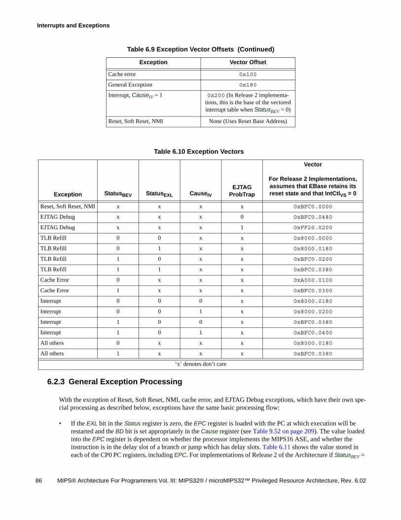
Interrupts and Exceptions
86 MIPS® Architecture For Programmers Vol. III: MIPS32® / microMIPS32™ Privileged Resource Architecture, Rev. 6.02
6.2.3 General Exception Processing
With the exception of Reset, Soft Reset, NMI, cache error, and EJTAG Debug exceptions, which have their own spe-cial processing as described below, exceptions have the same basic processing flow:
• If the EXL bit in the Status register is zero, the EPC register is loaded with the PC at which execution will be restarted and the BD bit is set appropriately in the Cause register (see Table 9.52 on page 209). The value loaded into the EPC register is dependent on whether the processor implements the MIPS16 ASE, and whether the instruction is in the delay slot of a branch or jump which has delay slots. Table 6.11 shows the value stored in each of the CP0 PC registers, including EPC. For implementations of Release 2 of the Architecture if StatusBEV =
Cache error 0x100
General Exception 0x180
Interrupt, CauseIV = 1 0x200 (In Release 2 implementa-tions, this is the base of the vectored interrupt table when StatusBEV = 0)
Reset, Soft Reset, NMI None (Uses Reset Base Address)
Table 6.10 Exception Vectors
Exception StatusBEV StatusEXL CauseIV
EJTAG ProbTrap
Vector
For Release 2 Implementations, assumes that EBase retains its reset state and that IntCtlVS = 0
Reset, Soft Reset, NMI x x x x 0xBFC0.0000
EJTAG Debug x x x 0 0xBFC0.0480
EJTAG Debug x x x 1 0xFF20.0200
TLB Refill 0 0 x x 0x8000.0000
TLB Refill 0 1 x x 0x8000.0180
TLB Refill 1 0 x x 0xBFC0.0200
TLB Refill 1 1 x x 0xBFC0.0380
Cache Error 0 x x x 0xA000.0100
Cache Error 1 x x x 0xBFC0.0300
Interrupt 0 0 0 x 0x8000.0180
Interrupt 0 0 1 x 0x8000.0200
Interrupt 1 0 0 x 0xBFC0.0380
Interrupt 1 0 1 x 0xBFC0.0400
All others 0 x x x 0x8000.0180
All others 1 x x x 0xBFC0.0380
‘x’ denotes don’t care
Table 6.9 Exception Vector Offsets (Continued)
Exception Vector Offset
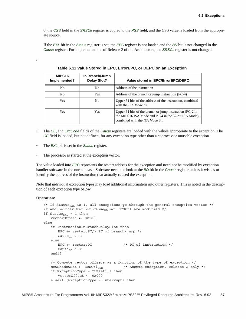
6.2 Exceptions
MIPS® Architecture For Programmers Vol. III: MIPS32® / microMIPS32™ Privileged Resource Architecture, Rev. 6.02 87
0, the CSS field in the SRSCtl register is copied to the PSS field, and the CSS value is loaded from the appropri-ate source.
If the EXL bit in the Status register is set, the EPC register is not loaded and the BD bit is not changed in the Cause register. For implementations of Release 2 of the Architecture, the SRSCtl register is not changed.
.
• The CE, and ExcCode fields of the Cause registers are loaded with the values appropriate to the exception. The CE field is loaded, but not defined, for any exception type other than a coprocessor unusable exception.
• The EXL bit is set in the Status register.
• The processor is started at the exception vector.
The value loaded into EPC represents the restart address for the exception and need not be modified by exception handler software in the normal case. Software need not look at the BD bit in the Cause register unless it wishes to identify the address of the instruction that actually caused the exception.
Note that individual exception types may load additional information into other registers. This is noted in the descrip-tion of each exception type below.
Operation:
/* If StatusEXL is 1, all exceptions go through the general exception vector *//* and neither EPC nor CauseBD nor SRSCtl are modified */if StatusEXL = 1 then
vectorOffset 0x180else
if InstructionInBranchDelaySlot thenEPC restartPC/* PC of branch/jump */CauseBD 1
elseEPC restartPC /* PC of instruction */CauseBD 0
endif
/* Compute vector offsets as a function of the type of exception */NewShadowSet SRSCtlESS /* Assume exception, Release 2 only */if ExceptionType = TLBRefill then
vectorOffset 0x000elseif (ExceptionType = Interrupt) then
Table 6.11 Value Stored in EPC, ErrorEPC, or DEPC on an Exception
MIPS16 Implemented?
In Branch/Jump Delay Slot? Value stored in EPC/ErrorEPC/DEPC
No No Address of the instruction
No Yes Address of the branch or jump instruction (PC-4)
Yes No Upper 31 bits of the address of the instruction, combined with the ISA Mode bit
Yes Yes Upper 31 bits of the branch or jump instruction (PC-2 in the MIPS16 ISA Mode and PC-4 in the 32-bit ISA Mode), combined with the ISA Mode bit
Interrupts and Exceptions
88 MIPS® Architecture For Programmers Vol. III: MIPS32® / microMIPS32™ Privileged Resource Architecture, Rev. 6.02
if (CauseIV = 0) thenvectorOffset 0x180
elseif (StatusBEV = 1) or (IntCtlVS = 0) then
vectorOffset 0x200else
if Config3VEIC = 1 thenif (EIC_option1)
VecNum CauseRIPLelseif (EIC_option2)
VecNum EIC_VecNum_SignalendifNewShadowSet SRSCtlEICSS
elseVecNum VIntPriorityEncoder()NewShadowSet SRSMapIPL4+3..IPL4
endifif (EIC_option3)
vectorOffset EIC_VectorOffset_Signalelse
vectorOffset 0x200 + (VecNum (IntCtlVS 0b00000))endif
endif /* if (StatusBEV = 1) or (IntCtlVS = 0) then */endif /* if (CauseIV = 0) then */
endif /* elseif (ExceptionType = Interrupt) then */
/* Update the shadow set information for an implementation of *//* Release 2 of the architecture */if (ArchitectureRevision 2) and (SRSCtlHSS 0) and (StatusBEV = 0) then
SRSCtlPSS SRSCtlCSSSRSCtlCSS NewShadowSet
endifendif /* if StatusEXL = 1 then */
CauseCE FaultingCoprocessorNumberCauseExcCode ExceptionTypeStatusEXL 1
/* Calculate the vector base address */if StatusBEV = 1 then
vectorBase 0xBFC0.0200else
if ArchitectureRevision 2 then/* The fixed value of EBase31..30 forces the base to be in kseg0 or kseg1 */vectorBase EBase31..12 0x000
elsevectorBase 0x8000.0000
endifendif
/* Exception PC is the sum of vectorBase and vectorOffset. Vector *//* offsets > 0xFFF (vectored or EIC interrupts only), require *//* that EBase15..12 have zeros in each bit position less than or *//* equal to the most significant bit position of the vector offset */PC vectorBase31..30 (vectorBase29..0 + vectorOffset29..0)
/* No carry between bits 29 and 30 */
6.2 Exceptions
MIPS® Architecture For Programmers Vol. III: MIPS32® / microMIPS32™ Privileged Resource Architecture, Rev. 6.02 89
6.2.4 EJTAG Debug Exception
An EJTAG Debug Exception occurs when one of a number of EJTAG-related conditions is met. Refer to the EJTAG Specification for details of this exception.
Entry Vector Used
0xBFC0 0480 if the ProbTrap bit is zero in the EJTAG_Control_register; 0xFF20 0200 if the ProbTrap bit isone.
6.2.5 Reset Exception
A Reset Exception occurs when the Cold Reset signal is asserted to the processor. This exception is not maskable. When a Reset Exception occurs, the processor performs a full reset initialization, including aborting state machines, establishing critical state, and generally placing the processor in a state in which it can execute instructions from uncached, unmapped address space. On a Reset Exception, only the following registers have defined state:
• The Random register is initialized to the number of TLB entries minus one. The Random register is deprecated in Release 6.
• The Wired register is initialized to zero.
• The Config, Config1, Config2, and Config3 registers are initialized with their boot state.
• The RP, BEV, TS, SR, NMI, and ERL fields of the Status register are initialized to a specified state.
• Watch register enables and Performance Counter register interrupt enables are cleared.
• The ErrorEPC register is loaded with the restart PC, as described in Table 6.11. Note that this value may or may not be predictable if the Reset Exception was taken as the result of power being applied to the processor because PC may not have a valid value in that case. In some implementations, the value loaded into ErrorEPC register may not be predictable on either a Reset or Soft Reset Exception.
• PC is loaded with 0xBFC0 0000.
Cause Register ExcCode Value
None
Additional State Saved
None
Entry Vector Used
Reset (0xBFC0 0000)
Operation
Random TLBEntries - 1PageMaskMaskX 0 # 1KB page support implementedPageGrainESP 0 # 1KB page support implementedWired 0HWREna 0EntryHiVPN2X 0 # 1KB page support implementedStatusRP 0 # This bit becomes reserved in Release 6StatusBEV 1
Interrupts and Exceptions
90 MIPS® Architecture For Programmers Vol. III: MIPS32® / microMIPS32™ Privileged Resource Architecture, Rev. 6.02
StatusTS 0 # This bit becomes reserved in Release 6StatusSR 0StatusNMI 0StatusERL 1IntCtlVS 0SRSCtlHSS HighestImplementedShadowSetSRSCtlESS 0SRSCtlPSS 0SRSCtlCSS 0SRSMap 0CauseDC 0EBaseExceptionBase 0Config ConfigurationStateConfigK0 2 # Suggested - see Config register descriptionConfig1 ConfigurationStateConfig2 ConfigurationStateConfig3 ConfigurationStateWatchLo[n]I 0 # For all implemented Watch registersWatchLo[n]R 0 # For all implemented Watch registersWatchLo[n]W 0 # For all implemented Watch registersPerfCnt.Control[n]IE 0 # For all implemented PerfCnt registersif InstructionInBranchDelaySlot then
ErrorEPC restartPC # PC of branch/jumpelse
ErrorEPC restartPC # PC of instructionendifPC 0xBFC0 0000
6.2.6 Soft Reset Exception
A Soft Reset Exception occurs when the Reset signal is asserted to the processor. This exception is not maskable. When a Soft Reset Exception occurs, the processor performs a subset of the full reset initialization. Although a Soft Reset Exception does not unnecessarily change the state of the processor, it may be forced to do so in order to place the processor in a state in which it can execute instructions from uncached, unmapped address space. Since bus, cache, or other operations may be interrupted, portions of the cache, memory, or other processor state may be incon-sistent.
The primary difference between the Reset and Soft Reset Exceptions is in actual use. The Reset Exception is typically used to initialize the processor on power-up, while the Soft Reset Exception is typically used to recover from a non-responsive (hung) processor. The semantic difference is provided to allow boot software to save critical coprocessor 0 or other register state to assist in debugging the potential problem. As such, the processor may reset the same state when either reset signal is asserted, but the interpretation of any state saved by software may be very different.
In addition to any hardware initialization required, the following state is established on a Soft Reset Exception:
• The RP, BEV, TS, SR, NMI, and ERL fields of the Status register are initialized to a specified state.
• Watch register enables and Performance Counter register interrupt enables are cleared.
• The ErrorEPC register is loaded with the restart PC, as described in Table 6.11.
• PC is loaded with 0xBFC0 0000.
Cause Register ExcCode Value
None
6.2 Exceptions
MIPS® Architecture For Programmers Vol. III: MIPS32® / microMIPS32™ Privileged Resource Architecture, Rev. 6.02 91
Additional State Saved
None
Entry Vector Used
Reset (0xBFC0 0000)
Operation
PageMaskMaskX 0 # 1KB page support implementedPageGrainESP 0 # 1KB page support implementedEntryHiVPN2X 0 # 1KB page support implementedConfigK0 2 # Suggested - see Config register descriptionStatusRP 0 # This bit becomes reserved in Release 6StatusBEV 1StatusTS 0 # This bit becomes reserved in Release 6StatusSR 1StatusNMI 0StatusERL 1WatchLo[n]I 0 # For all implemented Watch registersWatchLo[n]R 0 # For all implemented Watch registersWatchLo[n]W 0 # For all implemented Watch registersPerfCnt.Control[n]IE 0 # For all implemented PerfCnt registersif InstructionInBranchDelaySlot then
ErrorEPC restartPC # PC of branch/jumpelse
ErrorEPC restartPC # PC of instructionendifPC 0xBFC0 0000
6.2.7 Non Maskable Interrupt (NMI) Exception
A non maskable interrupt exception occurs when the NMI signal is asserted to the processor.
Although described as an interrupt, it is more correctly described as an exception because it is not maskable. An NMI occurs only at instruction boundaries, so does not do any reset or other hardware initialization. The state of the cache, memory, and other processor state is consistent and all registers are preserved, with the following exceptions:
• The BEV, TS, SR, NMI, and ERL fields of the Status register are initialized to a specified state.
• The ErrorEPC register is loaded with restart PC, as described in Table 6.11.
• PC is loaded with 0xBFC0 0000.
Cause Register ExcCode Value
None
Additional State Saved
None
Entry Vector Used
Reset (0xBFC0 0000)
Interrupts and Exceptions
92 MIPS® Architecture For Programmers Vol. III: MIPS32® / microMIPS32™ Privileged Resource Architecture, Rev. 6.02
Operation
StatusBEV 1StatusTS 0 # This bit becomes reserved in Release 6StatusSR 0StatusNMI 1StatusERL 1if InstructionInBranchDelaySlot then
ErrorEPC restartPC # PC of branch/jumpelse
ErrorEPC restartPC # PC of instructionendifPC 0xBFC0 0000
6.2.8 Machine Check Exception
A machine check exception occurs when the processor detects an internal inconsistency.
The following conditions cause a machine check exception:
• Detection of multiple matching entries in the TLB in a TLB-based MMU.If the Hardware Page Table Walker feature is implemented and the Directory-level Huge page feature is supported and the Dual Page method is also supported, and if the first accessed PTE entry has PTEVld bit set and the second accessed PTE entry has PTEVld bit clear.
Cause Register ExcCode Value
MCheck (See Table 9.53 on page 212)
Additional State Saved
Depends on the condition that caused the exception. See the descriptions above.
If there are multiple causes for the machine check exception, then the PageGrainMCCause register field is used to dis-
tinguish which condition caused the exception.
Entry Vector Used
General exception vector (offset 0x180)
6.2.9 Address Error Exception
An address error exception occurs under the following circumstances:
• An instruction is fetched from an address that is not aligned on a word boundary.
• A load or store word instruction is executed in which the address is not aligned on a word boundary.
• A load or store halfword instruction is executed in which the address is not aligned on a halfword boundary.
• A reference is made to a kernel address space from User Mode or Supervisor Mode.
• A reference is made to a supervisor address space from User Mode.
Release 6 supports misaligned load/store handling. Whether an Address Error is generated is implementation-depen-dent, as described in Appendix B of Volume I-A of the MIPS Architecture documentation set.
6.2 Exceptions
MIPS® Architecture For Programmers Vol. III: MIPS32® / microMIPS32™ Privileged Resource Architecture, Rev. 6.02 93
Note that in the case of an instruction fetch that is not aligned on a word boundary, the PC is updated before the con-dition is detected. Therefore, both EPC and BadVAddr point at the unaligned instruction address.
Cause Register ExcCode Value
AdEL: Reference was a load or an instruction fetch
AdES: Reference was a store
See Table 9.53 on page 212.
Additional State Saved
Entry Vector Used
General exception vector (offset 0x180)
6.2.10 TLB Refill Exception
A TLB Refill exception occurs in a TLB-based MMU when no TLB entry matches a reference to a mapped address space and the EXL bit is zero in the Status register. Note that this is distinct from the case in which an entry matches but has the valid bit off, in which case a TLB Invalid exception occurs.
Cause Register ExcCode Value
TLBL: Reference was a load or an instruction fetch
TLBS: Reference was a store
See Table 9.53 on page 212.
Additional State Saved
Register State Value
BadVAddr failing address
ContextVPN2 UNPREDICTABLE
EntryHiVPN2 UNPREDICTABLE
EntryLo0 UNPREDICTABLE
EntryLo1 UNPREDICTABLE
Register State Value
BadVAddr Failing address
Context If Config3CTXTC bit is set, then the bits of the Context reg-
ister corresponding to the set bits of the VirtualIndex field of the ContextConfig register are loaded with the high-order bits of the virtual address that missed.
If Config3CTXTC bit is clear, then the BadVPN2 field con-
tains VA31 13 of the failing address
EntryHi The VPN2 field contains VA31 13 of the failing address; the
ASID field contains the ASID of the reference that missed.
Interrupts and Exceptions
94 MIPS® Architecture For Programmers Vol. III: MIPS32® / microMIPS32™ Privileged Resource Architecture, Rev. 6.02
Entry Vector Used
• TLB Refill vector (offset 0x000) if StatusEXL = 0 at the time of exception.
• General exception vector (offset 0x180) if StatusEXL = 1 at the time of exception
6.2.11 Execute-Inhibit Exception
An Execute-Inhibit exception occurs when the virtual address of an instruction fetch matches a TLB entry whose XI bit is set. This exception type can only occur if the XI bit is implemented within the TLB and is enabled, this is denoted by the PageGrainXIE bit.
Cause Register ExcCode Value
if PageGrainIEC == 0 TLBL
if PageGrainIEC == 1 TLBXI
See Table 9.53 on page 212.
Additional State Saved
Entry Vector Used
General exception vector (offset 0x180)
6.2.12 Read-Inhibit Exception
An Read-Inhibit exception occurs when the virtual address of a memory load reference matches a TLB entry whose RI bit is set. This exception type can only occur if the RI bit is implemented within the TLB and is enabled, this is denoted by the PageGrainRIE bit. MIPS16 PC-relative loads are a special case and are not affected by the RI bit.
EntryLo0 UNPREDICTABLE
EntryLo1 UNPREDICTABLE
Register State Value
BadVAddr Failing address
Context If Config3CTXTC bit is set, then the bits of the Context reg-
ister corresponding to the set bits of the VirtualIndex field of the ContextConfig register are loaded with the high-order bits of the virtual address that missed.
If Config3CTXTC bit is clear, then the BadVPN2 field con-
tains VA31 13 of the failing address
EntryHi The VPN2 field contains VA31 13 of the failing address; the
ASID field contains the ASID of the reference that missed.
EntryLo0 UNPREDICTABLE
EntryLo1 UNPREDICTABLE
Register State Value
6.2 Exceptions
MIPS® Architecture For Programmers Vol. III: MIPS32® / microMIPS32™ Privileged Resource Architecture, Rev. 6.02 95
Cause Register ExcCode Value
if PageGrainIEC == 0 TLBL
if PageGrainIEC == 1 TLBRI
See Table 9.53 on page 212.
Additional State Saved
Entry Vector Used
General exception vector (offset 0x180)
6.2.13 TLB Invalid Exception
A TLB invalid exception occurs when a TLB entry matches a reference to a mapped address space, but the matched entry has the valid bit off.
Note that the condition in which no TLB entry matches a reference to a mapped address space and the EXL bit is one in the Status register is indistinguishable from a TLB Invalid Exception, in the sense that both use the general excep-tion vector and supply an ExcCode value of TLBL or TLBS. The only way to distinguish these two cases is by prob-ing the TLB for a matching entry (using TLBP).
If the RI and XI bits are implemented within the TLB and the PageGrainIEC bit is clear, then this exception also occurs if a valid, matching TLB entry is found with the RI bit set on a memory load reference, or with the XI bit set on an instruction fetch memory reference. MIPS16 PC-relative loads are a special case and are not affected by the RI bit.
Cause Register ExcCode Value
TLBL: Reference was a load or an instruction fetch
TLBS: Reference was a store
See Table 9.52 on page 209.
Register State Value
BadVAddr Failing address
Context If Config3CTXTC bit is set, then the bits of the Context reg-
ister corresponding to the set bits of the VirtualIndex field of the ContextConfig register are loaded with the high-order bits of the virtual address that missed.
If Config3CTXTC bit is clear, then the BadVPN2 field con-
tains VA31 13 of the failing address
EntryHi The VPN2 field contains VA31 13 of the failing address; the
ASID field contains the ASID of the reference that missed.
EntryLo0 UNPREDICTABLE
EntryLo1 UNPREDICTABLE
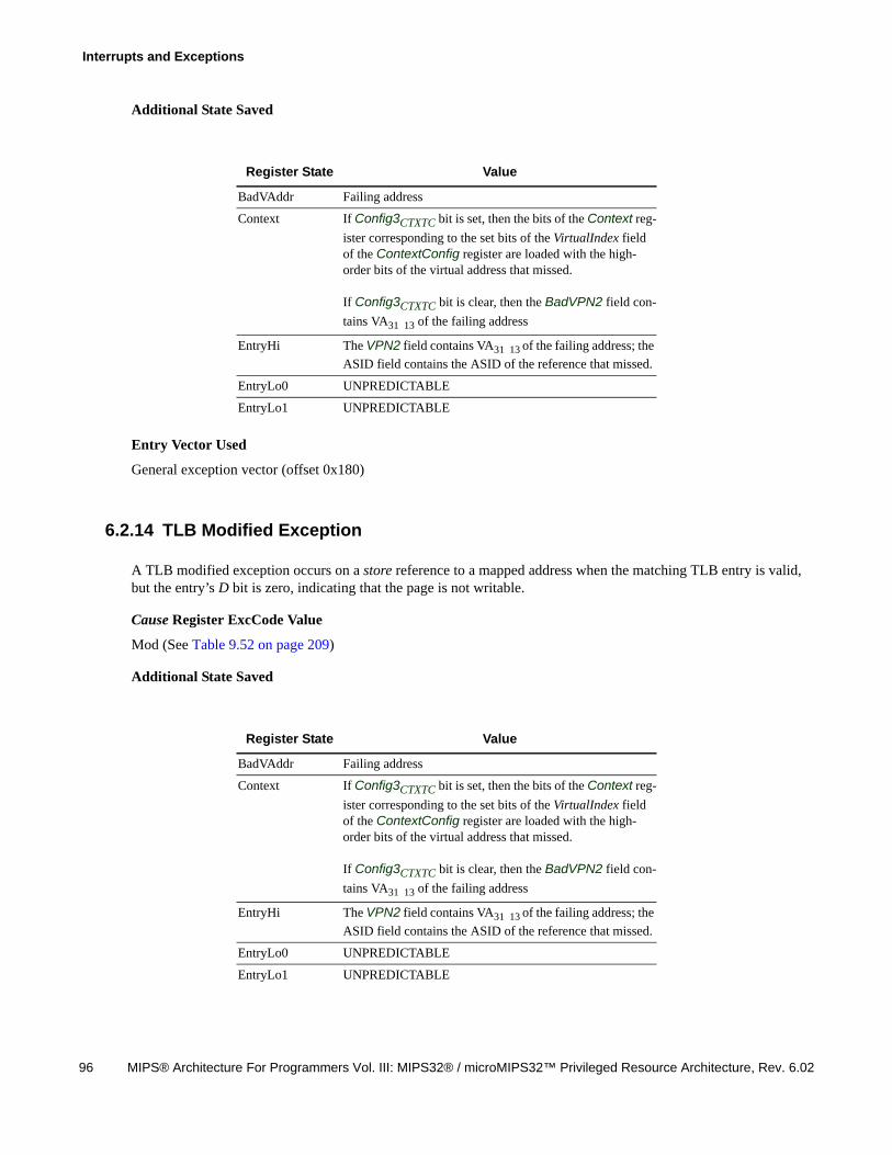
Interrupts and Exceptions
96 MIPS® Architecture For Programmers Vol. III: MIPS32® / microMIPS32™ Privileged Resource Architecture, Rev. 6.02
Additional State Saved
Entry Vector Used
General exception vector (offset 0x180)
6.2.14 TLB Modified Exception
A TLB modified exception occurs on a store reference to a mapped address when the matching TLB entry is valid, but the entry’s D bit is zero, indicating that the page is not writable.
Cause Register ExcCode Value
Mod (See Table 9.52 on page 209)
Additional State Saved
Register State Value
BadVAddr Failing address
Context If Config3CTXTC bit is set, then the bits of the Context reg-
ister corresponding to the set bits of the VirtualIndex field of the ContextConfig register are loaded with the high-order bits of the virtual address that missed.
If Config3CTXTC bit is clear, then the BadVPN2 field con-
tains VA31 13 of the failing address
EntryHi The VPN2 field contains VA31 13 of the failing address; the
ASID field contains the ASID of the reference that missed.
EntryLo0 UNPREDICTABLE
EntryLo1 UNPREDICTABLE
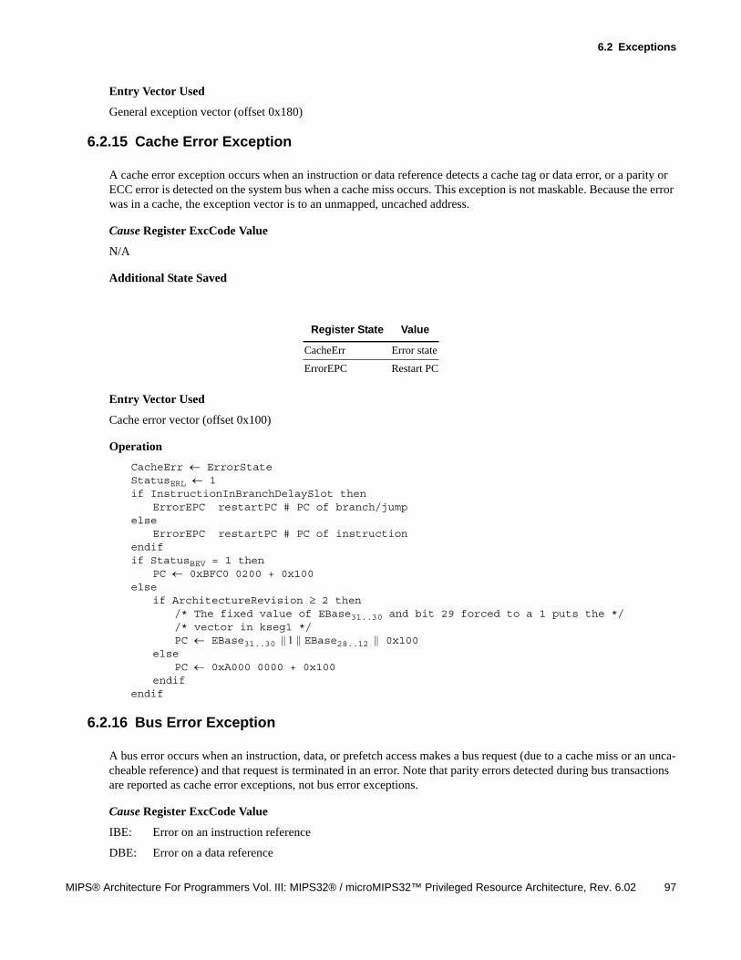
6.2 Exceptions
MIPS® Architecture For Programmers Vol. III: MIPS32® / microMIPS32™ Privileged Resource Architecture, Rev. 6.02 97
Entry Vector Used
General exception vector (offset 0x180)
6.2.15 Cache Error Exception
A cache error exception occurs when an instruction or data reference detects a cache tag or data error, or a parity or ECC error is detected on the system bus when a cache miss occurs. This exception is not maskable. Because the error was in a cache, the exception vector is to an unmapped, uncached address.
Cause Register ExcCode Value
N/A
Additional State Saved
Entry Vector Used
Cache error vector (offset 0x100)
Operation
CacheErr ErrorStateStatusERL 1if InstructionInBranchDelaySlot then
ErrorEPC restartPC # PC of branch/jumpelse
ErrorEPC restartPC # PC of instructionendifif StatusBEV = 1 then
PC 0xBFC0 0200 + 0x100else
if ArchitectureRevision 2 then/* The fixed value of EBase31..30 and bit 29 forced to a 1 puts the *//* vector in kseg1 */PC EBase31..30 EBase28..12 0x100
elsePC 0xA000 0000 + 0x100
endifendif
6.2.16 Bus Error Exception
A bus error occurs when an instruction, data, or prefetch access makes a bus request (due to a cache miss or an unca-cheable reference) and that request is terminated in an error. Note that parity errors detected during bus transactions are reported as cache error exceptions, not bus error exceptions.
Cause Register ExcCode Value
IBE: Error on an instruction reference
DBE: Error on a data reference
Register State Value
CacheErr Error state
ErrorEPC Restart PC
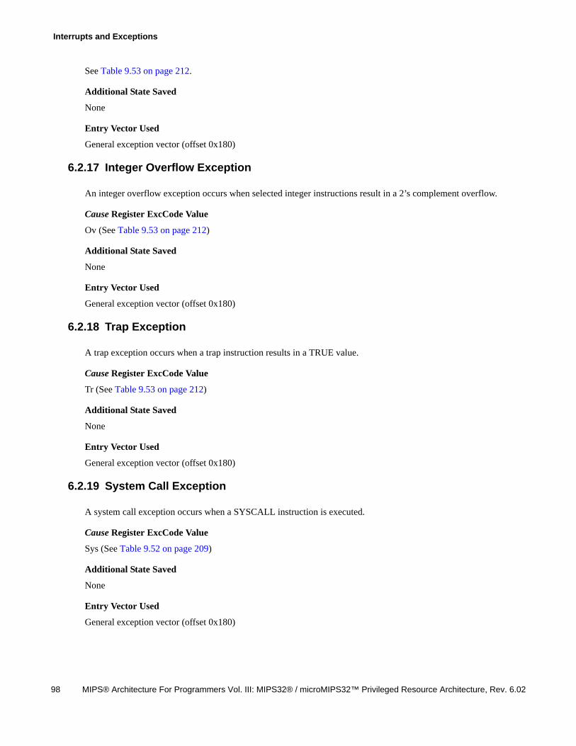
Interrupts and Exceptions
98 MIPS® Architecture For Programmers Vol. III: MIPS32® / microMIPS32™ Privileged Resource Architecture, Rev. 6.02
See Table 9.53 on page 212.
Additional State Saved
None
Entry Vector Used
General exception vector (offset 0x180)
6.2.17 Integer Overflow Exception
An integer overflow exception occurs when selected integer instructions result in a 2’s complement overflow.
Cause Register ExcCode Value
Ov (See Table 9.53 on page 212)
Additional State Saved
None
Entry Vector Used
General exception vector (offset 0x180)
6.2.18 Trap Exception
A trap exception occurs when a trap instruction results in a TRUE value.
Cause Register ExcCode Value
Tr (See Table 9.53 on page 212)
Additional State Saved
None
Entry Vector Used
General exception vector (offset 0x180)
6.2.19 System Call Exception
A system call exception occurs when a SYSCALL instruction is executed.
Cause Register ExcCode Value
Sys (See Table 9.52 on page 209)
Additional State Saved
None
Entry Vector Used
General exception vector (offset 0x180)
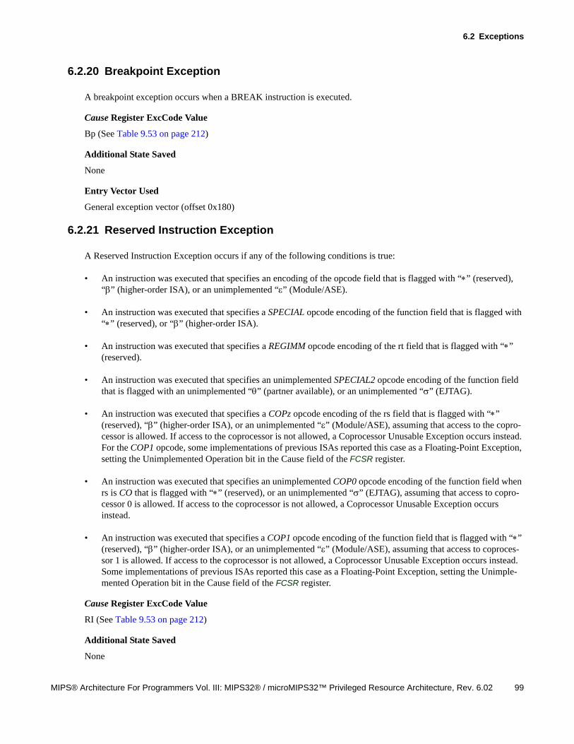
6.2 Exceptions
MIPS® Architecture For Programmers Vol. III: MIPS32® / microMIPS32™ Privileged Resource Architecture, Rev. 6.02 99
6.2.20 Breakpoint Exception
A breakpoint exception occurs when a BREAK instruction is executed.
Cause Register ExcCode Value
Bp (See Table 9.53 on page 212)
Additional State Saved
None
Entry Vector Used
General exception vector (offset 0x180)
6.2.21 Reserved Instruction Exception
A Reserved Instruction Exception occurs if any of the following conditions is true:
• An instruction was executed that specifies an encoding of the opcode field that is flagged with “” (reserved), “” (higher-order ISA), or an unimplemented “” (Module/ASE).
• An instruction was executed that specifies a SPECIAL opcode encoding of the function field that is flagged with “” (reserved), or “” (higher-order ISA).
• An instruction was executed that specifies a REGIMM opcode encoding of the rt field that is flagged with “”(reserved).
• An instruction was executed that specifies an unimplemented SPECIAL2 opcode encoding of the function field that is flagged with an unimplemented “” (partner available), or an unimplemented “” (EJTAG).
• An instruction was executed that specifies a COPz opcode encoding of the rs field that is flagged with “” (reserved), “” (higher-order ISA), or an unimplemented “” (Module/ASE), assuming that access to the copro-cessor is allowed. If access to the coprocessor is not allowed, a Coprocessor Unusable Exception occurs instead. For the COP1 opcode, some implementations of previous ISAs reported this case as a Floating-Point Exception, setting the Unimplemented Operation bit in the Cause field of the FCSR register.
• An instruction was executed that specifies an unimplemented COP0 opcode encoding of the function field when rs is CO that is flagged with “” (reserved), or an unimplemented “” (EJTAG), assuming that access to copro-cessor 0 is allowed. If access to the coprocessor is not allowed, a Coprocessor Unusable Exception occurs instead.
• An instruction was executed that specifies a COP1 opcode encoding of the function field that is flagged with “” (reserved), “” (higher-order ISA), or an unimplemented “” (Module/ASE), assuming that access to coproces-sor 1 is allowed. If access to the coprocessor is not allowed, a Coprocessor Unusable Exception occurs instead. Some implementations of previous ISAs reported this case as a Floating-Point Exception, setting the Unimple-mented Operation bit in the Cause field of the FCSR register.
Cause Register ExcCode Value
RI (See Table 9.53 on page 212)
Additional State Saved
None
Interrupts and Exceptions
100 MIPS® Architecture For Programmers Vol. III: MIPS32® / microMIPS32™ Privileged Resource Architecture, Rev. 6.02
Entry Vector Used
General exception vector (offset 0x180)
6.2.22 Coprocessor Unusable Exception
A coprocessor unusable exception occurs if any of the following conditions is true:
• A COP0 or Cache instruction was executed while the processor was running in a mode other than Debug Mode or Kernel Mode, and the CU0 bit in the Status register was a zero
• A COP1, COP1X,LWC1, SWC1, LDC1, SDC1 or MOVCI (Special opcode function field encoding) instruction was executed and the CU1 bit in the Status register was a zero.
• A COP2, LWC2, SWC2, LDC2, or SDC2 instruction was executed, and the CU2 bit in the Status register was a zero. COP2 instructions include MFC2, DMFC2, CFC2, MFHC2, MTC2, DMTC2, CTC2, MTHC2.
NOTE: In Release 2 of the MIPS32 Architecture, the use of COP3 as a user-defined coprocessor has been removed. The use of COP3 is reserved for the future extension of the architecture.
Cause Register ExcCode Value
CpU (See Table 9.52 on page 209)
Additional State Saved
Entry Vector Used
General exception vector (offset 0x180)
6.2.23 Floating-Point Exception
A floating-point exception is initiated by the floating-point coprocessor to signal a floating-point exception.
Register ExcCode Value
FPE (See Table 9.52 on page 209)
Additional State Saved
Entry Vector Used
General exception vector (offset 0x180)
Register State Value
CauseCE unit number of the coprocessor being referenced
Register State Value
FCSR indicates the cause of the floating-point exception
6.2 Exceptions
MIPS® Architecture For Programmers Vol. III: MIPS32® / microMIPS32™ Privileged Resource Architecture, Rev. 6.02 101
6.2.24 Coprocessor 2 Exception
A coprocessor 2 exception is initiated by coprocessor 2 to signal a precise coprocessor 2 exception.
Register ExcCode Value
C2E (See Table 9.52 on page 209)
Additional State Saved
Defined by the coprocessor
Entry Vector Used
General exception vector (offset 0x180)
6.2.25 Watch Exception
The watch facility provides a software debugging vehicle by initiating a watch exception when an instruction or data reference matches the address information stored in the WatchHi and WatchLo registers. A watch exception is taken immediately if the EXL and ERL bits of the Status register are both zero. If either bit is a one at the time that a watch exception would normally be taken, the WP bit in the Cause register is set, and the exception is deferred until both the EXL and ERL bits in the Status register are zero. Software may use the WP bit in the Cause register to determine if the EPC register points at the instruction that caused the watch exception, or if the exception actually occurred while in kernel mode.
If the EXL or ERL bits are one in the Status register and a single instruction generates both a watch exception (which is deferred by the state of the EXL and ERL bits) and a lower-priority exception, the lower priority exception is taken.
Watch exceptions are never taken if the processor is executing in Debug Mode. Should a watch register match while the processor is in Debug Mode, the exception is inhibited and the WP bit is not changed.
It is implementation-dependent whether a data watch exception is triggered by a prefetch or cache instruction whose address matches the Watch register address match conditions. A watch triggered by a SC instruction does so even if the store would not complete because the LL bit is zero.
Register ExcCode Value
WATCH (See Table 9.52 on page 209)
Additional State Saved
Entry Vector Used
General exception vector (offset 0x180)
Register State Value
CauseWP Indicates that the watch exception was deferred until after both StatusEXL and StatusERL were zero. This bit directly
causes a watch exception, so software must clear this bit as part of the exception handler to prevent a watch exception loop at the end of the current handler execution.
Interrupts and Exceptions
102 MIPS® Architecture For Programmers Vol. III: MIPS32® / microMIPS32™ Privileged Resource Architecture, Rev. 6.02
6.2.26 Interrupt Exception
The interrupt exception occurs when an enabled request for interrupt service is made. See Section 6.1 on page 71 for more information.
Register ExcCode Value
Int (See Table 9.53 on page 212)
Additional State Saved
Entry Vector Used
General exception vector (offset 0x180) if the IV bit in the Cause register is zero.
Interrupt vector (offset 0x200) if the IV bit in the Cause register is one.
Register State Value
CauseIP indicates the interrupts that are pending.
Chapter 7
MIPS® Architecture For Programmers Vol. III: MIPS32® / microMIPS32™ Privileged Resource Architecture, Rev. 6.02 103
GPR Shadow Registers
The capability in this chapter is targeted at removing the need to save and restore GPRs on entry to high priority inter-rupts or exceptions, and to provide specified processor modes with the same capability. This is done by introducing multiple copies of the GPRs, called shadow sets, and allowing privileged software to associate a shadow set with entry to Kernel Mode via an interrupt vector or exception. The normal GPRs are logically considered shadow set zero.
The number of GPR shadow sets is implementation-dependent and may range from one (the normal GPRs) to an architectural maximum of 16. The highest number actually implemented is indicated by the SRSCtlHSS field, and all
shadow sets between 0 and SRSCtlHSS, inclusive must be implemented. If this field is zero, only the normal GPRs are
implemented.
7.1 Introduction to Shadow Sets
Shadow sets are new copies of the GPRs that can be substituted for the normal GPRs on entry to Kernel Mode via an interrupt or exception. Once a shadow set is bound to a Kernel Mode entry condition, reference to GPRs work exactly as one would expect, but they are redirected to registers that are dedicated to that condition. Privileged software may need to reference all GPRs in the register file, even specific shadow registers that are not visible in the current mode. The RDPGPR and WRPGPR instructions are used for this purpose. The CSS field of the SRSCtl register provides the number of the current shadow register set, and the PSS field of the SRSCtl register provides the number of the previ-ous shadow register set (that which was current before the last exception or interrupt occurred).
If the processor is operating in VI interrupt mode, binding of a vectored interrupt to a shadow set is done by writing to the SRSMap register. If the processor is operating in EIC interrupt mode, the binding of the interrupt to a specific shadow set is provided by the external interrupt controller, and is configured in an implementation-dependent way. Binding of an exception or non-vectored interrupt to a shadow set is done by writing to the ESS field of the SRSCtl register. When an exception or interrupt occurs, the value of SRSCtlCSS is copied to SRSCtlPSS, and SRSCtlCSS is set
to the value taken from the appropriate source. On an ERET, the value of SRSCtlPSS is copied back into SRSCtlCSS to
restore the shadow set of the mode to which control returns. More precisely, the rules for updating the fields in the SRSCtl register on an interrupt or exception are as follows:
1. No field in the SRSCtl register is updated if any of the following conditions are true. In this case, steps 2 and 3 are skipped.
• The exception is one that sets StatusERL: NMI or cache error.
• The exception causes entry into EJTAG Debug Mode
• StatusBEV = 1
• StatusEXL = 1
2. SRSCtlCSS is copied to SRSCtlPSS
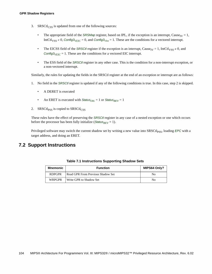
GPR Shadow Registers
104 MIPS® Architecture For Programmers Vol. III: MIPS32® / microMIPS32™ Privileged Resource Architecture, Rev. 6.02
3. SRSCtlCSS is updated from one of the following sources:
• The appropriate field of the SRSMap register, based on IPL, if the exception is an interrupt, CauseIV = 1,
IntCtlVSS 0, Config3VEIC = 0, and Config3VInt = 1. These are the conditions for a vectored interrupt.
• The EICSS field of the SRSCtl register if the exception is an interrupt, CauseIV = 1, IntCtlVSS 0, and
Config3VEIC = 1. These are the conditions for a vectored EIC interrupt.
• The ESS field of the SRSCtl register in any other case. This is the condition for a non-interrupt exception, or a non-vectored interrupt.
Similarly, the rules for updating the fields in the SRSCtl register at the end of an exception or interrupt are as follows:
1. No field in the SRSCtl register is updated if any of the following conditions is true. In this case, step 2 is skipped.
• A DERET is executed
• An ERET is executed with StatusERL = 1 or StatusBEV = 1
2. SRSCtlPSS is copied to SRSCtlCSS
These rules have the effect of preserving the SRSCtl register in any case of a nested exception or one which occurs before the processor has been fully initialize (StatusBEV = 1).
Privileged software may switch the current shadow set by writing a new value into SRSCtlPSS, loading EPC with a
target address, and doing an ERET.
7.2 Support Instructions
Table 7.1 Instructions Supporting Shadow Sets
Mnemonic Function MIPS64 Only?
RDPGPR Read GPR From Previous Shadow Set No
WRPGPR Write GPR to Shadow Set No
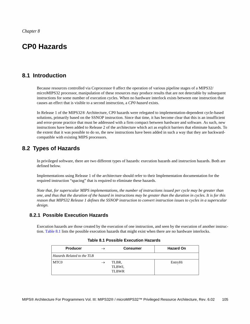
Chapter 8
MIPS® Architecture For Programmers Vol. III: MIPS32® / microMIPS32™ Privileged Resource Architecture, Rev. 6.02 105
CP0 Hazards
8.1 Introduction
Because resources controlled via Coprocessor 0 affect the operation of various pipeline stages of a MIPS32/microMIPS32 processor, manipulation of these resources may produce results that are not detectable by subsequent instructions for some number of execution cycles. When no hardware interlock exists between one instruction that causes an effect that is visible to a second instruction, a CP0 hazard exists.
In Release 1 of the MIPS32® Architecture, CP0 hazards were relegated to implementation-dependent cycle-based solutions, primarily based on the SSNOP instruction. Since that time, it has become clear that this is an insufficient and error-prone practice that must be addressed with a firm compact between hardware and software. As such, new instructions have been added to Release 2 of the architecture which act as explicit barriers that eliminate hazards. To the extent that it was possible to do so, the new instructions have been added in such a way that they are backward-compatible with existing MIPS processors.
8.2 Types of Hazards
In privileged software, there are two different types of hazards: execution hazards and instruction hazards. Both are defined below.
Implementations using Release 1 of the architecture should refer to their Implementation documentation for the required instruction “spacing” that is required to eliminate these hazards.
Note that, for superscalar MIPS implementations, the number of instructions issued per cycle may be greater than one, and thus that the duration of the hazard in instructions may be greater than the duration in cycles. It is for this reason that MIPS32 Release 1 defines the SSNOP instruction to convert instruction issues to cycles in a superscalar design.
8.2.1 Possible Execution Hazards
Execution hazards are those created by the execution of one instruction, and seen by the execution of another instruc-tion. Table 8.1 lists the possible execution hazards that might exist when there are no hardware interlocks.
Table 8.1 Possible Execution Hazards
Producer Consumer Hazard On
Hazards Related to the TLB
MTC0 TLBR,TLBWI,TLBWR
EntryHi
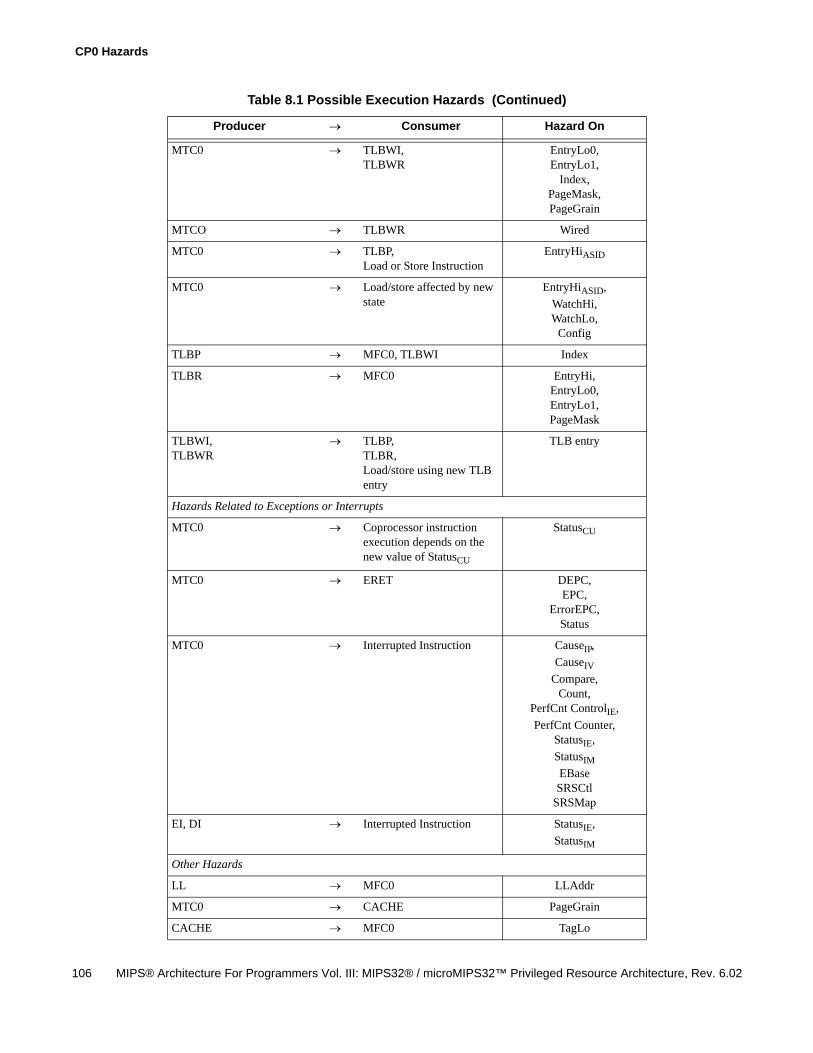
CP0 Hazards
106 MIPS® Architecture For Programmers Vol. III: MIPS32® / microMIPS32™ Privileged Resource Architecture, Rev. 6.02
MTC0 TLBWI,TLBWR
EntryLo0,EntryLo1,
Index,PageMask,PageGrain
MTCO TLBWR Wired
MTC0 TLBP,Load or Store Instruction
EntryHiASID
MTC0 Load/store affected by new state
EntryHiASID,
WatchHi,WatchLo,
Config
TLBP MFC0, TLBWI Index
TLBR MFC0 EntryHi,EntryLo0,EntryLo1,PageMask
TLBWI, TLBWR
TLBP, TLBR,Load/store using new TLB entry
TLB entry
Hazards Related to Exceptions or Interrupts
MTC0 Coprocessor instruction execution depends on the new value of StatusCU
StatusCU
MTC0 ERET DEPC,EPC,
ErrorEPC,Status
MTC0 Interrupted Instruction CauseIP,
CauseIV
Compare,Count,
PerfCnt ControlIE,
PerfCnt Counter,StatusIE,
StatusIM
EBaseSRSCtl
SRSMap
EI, DI Interrupted Instruction StatusIE,
StatusIM
Other Hazards
LL MFC0 LLAddr
MTC0 CACHE PageGrain
CACHE MFC0 TagLo
Table 8.1 Possible Execution Hazards (Continued)
Producer Consumer Hazard On
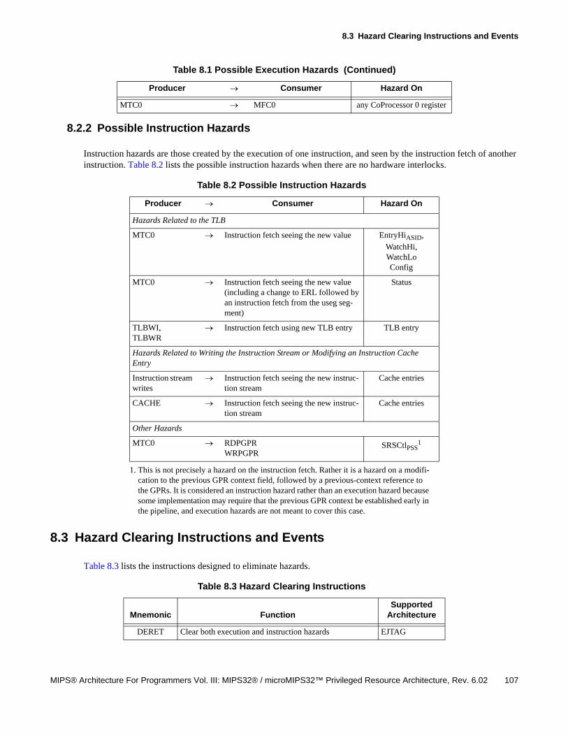
8.3 Hazard Clearing Instructions and Events
MIPS® Architecture For Programmers Vol. III: MIPS32® / microMIPS32™ Privileged Resource Architecture, Rev. 6.02 107
8.2.2 Possible Instruction Hazards
Instruction hazards are those created by the execution of one instruction, and seen by the instruction fetch of another instruction. Table 8.2 lists the possible instruction hazards when there are no hardware interlocks.
8.3 Hazard Clearing Instructions and Events
Table 8.3 lists the instructions designed to eliminate hazards.
MTC0 MFC0 any CoProcessor 0 register
Table 8.2 Possible Instruction Hazards
Producer Consumer Hazard On
Hazards Related to the TLB
MTC0 Instruction fetch seeing the new value EntryHiASID,
WatchHi,WatchLoConfig
MTC0 Instruction fetch seeing the new value (including a change to ERL followed by an instruction fetch from the useg seg-ment)
Status
TLBWI,TLBWR
Instruction fetch using new TLB entry TLB entry
Hazards Related to Writing the Instruction Stream or Modifying an Instruction Cache Entry
Instruction stream writes
Instruction fetch seeing the new instruc-tion stream
Cache entries
CACHE Instruction fetch seeing the new instruc-tion stream
Cache entries
Other Hazards
MTC0 RDPGPRWRPGPR
SRSCtlPSS1
1. This is not precisely a hazard on the instruction fetch. Rather it is a hazard on a modifi-cation to the previous GPR context field, followed by a previous-context reference to the GPRs. It is considered an instruction hazard rather than an execution hazard because some implementation may require that the previous GPR context be established early in the pipeline, and execution hazards are not meant to cover this case.
Table 8.3 Hazard Clearing Instructions
Mnemonic FunctionSupported
Architecture
DERET Clear both execution and instruction hazards EJTAG
Table 8.1 Possible Execution Hazards (Continued)
Producer Consumer Hazard On
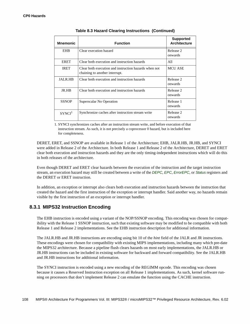
CP0 Hazards
108 MIPS® Architecture For Programmers Vol. III: MIPS32® / microMIPS32™ Privileged Resource Architecture, Rev. 6.02
DERET, ERET, and SSNOP are available in Release 1 of the Architecture; EHB, JALR.HB, JR.HB, and SYNCI were added in Release 2 of the Architecture. In both Release 1 and Release 2 of the Architecture, DERET and ERET clear both execution and instruction hazards and they are the only timing-independent instructions which will do this in both releases of the architecture.
Even though DERET and ERET clear hazards between the execution of the instruction and the target instruction stream, an execution hazard may still be created between a write of the DEPC, EPC, ErrorEPC, or Status registers and the DERET or ERET instruction.
In addition, an exception or interrupt also clears both execution and instruction hazards between the instruction that created the hazard and the first instruction of the exception or interrupt handler. Said another way, no hazards remain visible by the first instruction of an exception or interrupt handler.
8.3.1 MIPS32 Instruction Encoding
The EHB instruction is encoded using a variant of the NOP/SSNOP encoding. This encoding was chosen for compat-ibility with the Release 1 SSNOP instruction, such that existing software may be modified to be compatible with both Release 1 and Release 2 implementations. See the EHB instruction description for additional information.
The JALR.HB and JR.HB instructions are encoding using bit 10 of the hint field of the JALR and JR instructions. These encodings were chosen for compatibility with existing MIPS implementations, including many which pre-date the MIPS32 architecture. Because a pipeline flush clears hazards on most early implementations, the JALR.HB or JR.HB instructions can be included in existing software for backward and forward compatibility. See the JALR.HB and JR.HB instructions for additional information.
The SYNCI instruction is encoded using a new encoding of the REGIMM opcode. This encoding was chosen because it causes a Reserved Instruction exception on all Release 1 implementations. As such, kernel software run-ning on processors that don’t implement Release 2 can emulate the function using the CACHE instruction.
EHB Clear execution hazard Release 2 onwards
ERET Clear both execution and instruction hazards All
IRET Clear both execution and instruction hazards when not chaining to another interrupt.
MCU ASE
JALR.HB Clear both execution and instruction hazards Release 2 onwards
JR.HB Clear both execution and instruction hazards Release 2 onwards
SSNOP Superscalar No Operation Release 1 onwards
SYNCI1 Synchronize caches after instruction stream write Release 2 onwards
1. SYNCI synchronizes caches after an instruction stream write, and before execution of that instruction stream. As such, it is not precisely a coprocessor 0 hazard, but is included here for completeness.
Table 8.3 Hazard Clearing Instructions (Continued)
Mnemonic FunctionSupported
Architecture
8.3 Hazard Clearing Instructions and Events
MIPS® Architecture For Programmers Vol. III: MIPS32® / microMIPS32™ Privileged Resource Architecture, Rev. 6.02 109
8.3.2 microMIPS32 Instruction Encoding
The EHB and SSNOP instructions are encoded using a variant of the NOP encoding. See the EHB and SSNOP instruction description for additional information.

CP0 Hazards
110 MIPS® Architecture For Programmers Vol. III: MIPS32® / microMIPS32™ Privileged Resource Architecture, Rev. 6.02
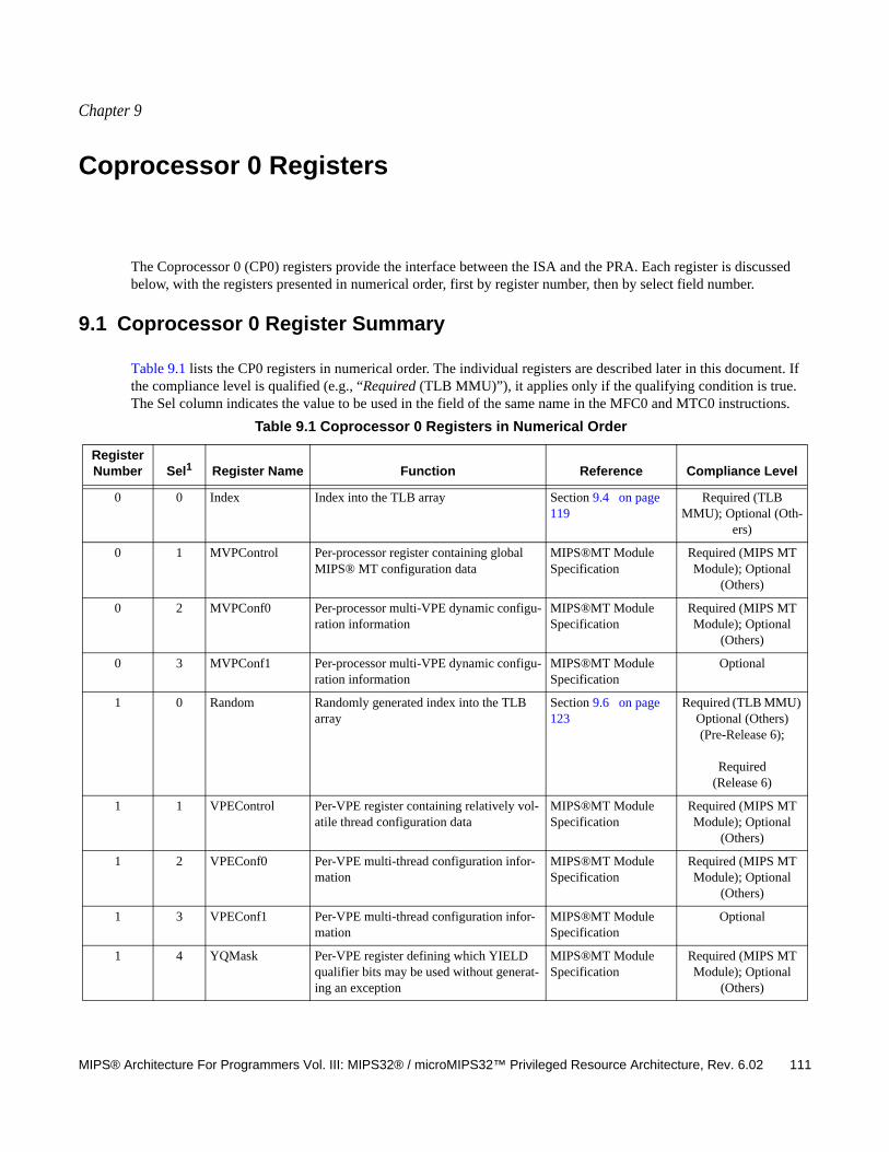
Chapter 9
MIPS® Architecture For Programmers Vol. III: MIPS32® / microMIPS32™ Privileged Resource Architecture, Rev. 6.02 111
Coprocessor 0 Registers
The Coprocessor 0 (CP0) registers provide the interface between the ISA and the PRA. Each register is discussed below, with the registers presented in numerical order, first by register number, then by select field number.
9.1 Coprocessor 0 Register Summary
Table 9.1 lists the CP0 registers in numerical order. The individual registers are described later in this document. If the compliance level is qualified (e.g., “Required (TLB MMU)”), it applies only if the qualifying condition is true. The Sel column indicates the value to be used in the field of the same name in the MFC0 and MTC0 instructions.
Table 9.1 Coprocessor 0 Registers in Numerical Order
Register Number Sel1 Register Name Function Reference Compliance Level
0 0 Index Index into the TLB array Section 9.4 on page 119
Required (TLB MMU); Optional (Oth-
ers)
0 1 MVPControl Per-processor register containing global MIPS® MT configuration data
MIPS®MT Module Specification
Required (MIPS MT Module); Optional
(Others)
0 2 MVPConf0 Per-processor multi-VPE dynamic configu-ration information
MIPS®MT Module Specification
Required (MIPS MT Module); Optional
(Others)
0 3 MVPConf1 Per-processor multi-VPE dynamic configu-ration information
MIPS®MT Module Specification
Optional
1 0 Random Randomly generated index into the TLB array
Section 9.6 on page 123
Required (TLB MMU) Optional (Others) (Pre-Release 6);
Required(Release 6)
1 1 VPEControl Per-VPE register containing relatively vol-atile thread configuration data
MIPS®MT Module Specification
Required (MIPS MT Module); Optional
(Others)
1 2 VPEConf0 Per-VPE multi-thread configuration infor-mation
MIPS®MT Module Specification
Required (MIPS MT Module); Optional
(Others)
1 3 VPEConf1 Per-VPE multi-thread configuration infor-mation
MIPS®MT Module Specification
Optional
1 4 YQMask Per-VPE register defining which YIELD qualifier bits may be used without generat-ing an exception
MIPS®MT Module Specification
Required (MIPS MT Module); Optional
(Others)
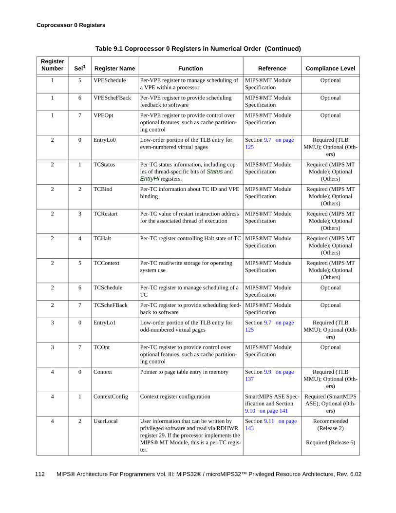
Coprocessor 0 Registers
112 MIPS® Architecture For Programmers Vol. III: MIPS32® / microMIPS32™ Privileged Resource Architecture, Rev. 6.02
1 5 VPESchedule Per-VPE register to manage scheduling of a VPE within a processor
MIPS®MT Module Specification
Optional
1 6 VPEScheFBack Per-VPE register to provide scheduling feedback to software
MIPS®MT Module Specification
Optional
1 7 VPEOpt Per-VPE register to provide control over optional features, such as cache partition-ing control
MIPS®MT Module Specification
Optional
2 0 EntryLo0 Low-order portion of the TLB entry for even-numbered virtual pages
Section 9.7 on page 125
Required (TLB MMU); Optional (Oth-
ers)
2 1 TCStatus Per-TC status information, including cop-ies of thread-specific bits of Status and EntryHi registers.
MIPS®MT Module Specification
Required (MIPS MT Module); Optional
(Others)
2 2 TCBind Per-TC information about TC ID and VPE binding
MIPS®MT Module Specification
Required (MIPS MT Module); Optional
(Others)
2 3 TCRestart Per-TC value of restart instruction address for the associated thread of execution
MIPS®MT Module Specification
Required (MIPS MT Module); Optional
(Others)
2 4 TCHalt Per-TC register controlling Halt state of TC MIPS®MT Module Specification
Required (MIPS MT Module); Optional
(Others)
2 5 TCContext Per-TC read/write storage for operating system use
MIPS®MT Module Specification
Required (MIPS MT Module); Optional
(Others)
2 6 TCSchedule Per-TC register to manage scheduling of a TC
MIPS®MT Module Specification
Optional
2 7 TCScheFBack Per-TC register to provide scheduling feed-back to software
MIPS®MT Module Specification
Optional
3 0 EntryLo1 Low-order portion of the TLB entry for odd-numbered virtual pages
Section 9.7 on page 125
Required (TLB MMU); Optional (Oth-
ers)
3 7 TCOpt Per-TC register to provide control over optional features, such as cache partition-ing control
MIPS®MT Module Specification
Optional
4 0 Context Pointer to page table entry in memory Section 9.9 on page 137
Required (TLB MMU); Optional (Oth-
ers)
4 1 ContextConfig Context register configuration SmartMIPS ASE Spec-ification and Section 9.10 on page 141
Required (SmartMIPS ASE); Optional (Oth-
ers)
4 2 UserLocal User information that can be written by privileged software and read via RDHWR register 29. If the processor implements the MIPS® MT Module, this is a per-TC regis-ter.
Section 9.11 on page 143
Recommended (Release 2)
Required (Release 6)
Table 9.1 Coprocessor 0 Registers in Numerical Order (Continued)
Register Number Sel1 Register Name Function Reference Compliance Level
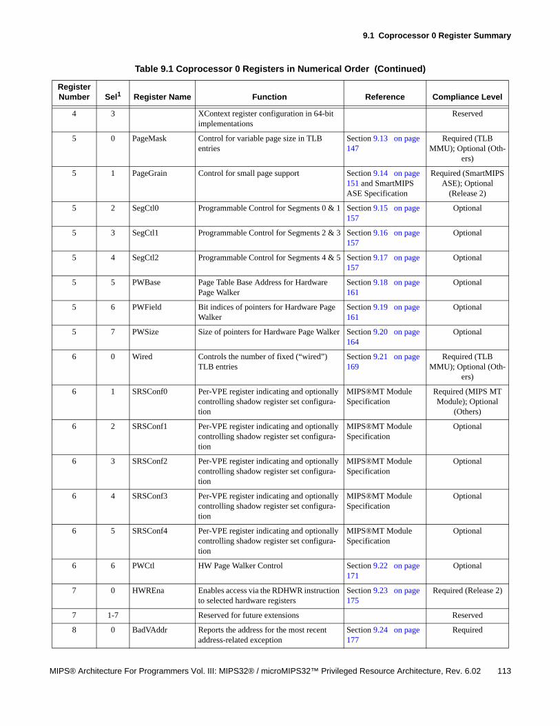
9.1 Coprocessor 0 Register Summary
MIPS® Architecture For Programmers Vol. III: MIPS32® / microMIPS32™ Privileged Resource Architecture, Rev. 6.02 113
4 3 XContext register configuration in 64-bit implementations
Reserved
5 0 PageMask Control for variable page size in TLB entries
Section 9.13 on page 147
Required (TLB MMU); Optional (Oth-
ers)
5 1 PageGrain Control for small page support Section 9.14 on page 151 and SmartMIPS ASE Specification
Required (SmartMIPS ASE); Optional
(Release 2)
5 2 SegCtl0 Programmable Control for Segments 0 & 1 Section 9.15 on page 157
Optional
5 3 SegCtl1 Programmable Control for Segments 2 & 3 Section 9.16 on page 157
Optional
5 4 SegCtl2 Programmable Control for Segments 4 & 5 Section 9.17 on page 157
Optional
5 5 PWBase Page Table Base Address for Hardware Page Walker
Section 9.18 on page 161
Optional
5 6 PWField Bit indices of pointers for Hardware Page Walker
Section 9.19 on page 161
Optional
5 7 PWSize Size of pointers for Hardware Page Walker Section 9.20 on page 164
Optional
6 0 Wired Controls the number of fixed (“wired”) TLB entries
Section 9.21 on page 169
Required (TLB MMU); Optional (Oth-
ers)
6 1 SRSConf0 Per-VPE register indicating and optionally controlling shadow register set configura-tion
MIPS®MT Module Specification
Required (MIPS MT Module); Optional
(Others)
6 2 SRSConf1 Per-VPE register indicating and optionally controlling shadow register set configura-tion
MIPS®MT Module Specification
Optional
6 3 SRSConf2 Per-VPE register indicating and optionally controlling shadow register set configura-tion
MIPS®MT Module Specification
Optional
6 4 SRSConf3 Per-VPE register indicating and optionally controlling shadow register set configura-tion
MIPS®MT Module Specification
Optional
6 5 SRSConf4 Per-VPE register indicating and optionally controlling shadow register set configura-tion
MIPS®MT Module Specification
Optional
6 6 PWCtl HW Page Walker Control Section 9.22 on page 171
Optional
7 0 HWREna Enables access via the RDHWR instruction to selected hardware registers
Section 9.23 on page 175
Required (Release 2)
7 1-7 Reserved for future extensions Reserved
8 0 BadVAddr Reports the address for the most recent address-related exception
Section 9.24 on page 177
Required
Table 9.1 Coprocessor 0 Registers in Numerical Order (Continued)
Register Number Sel1 Register Name Function Reference Compliance Level
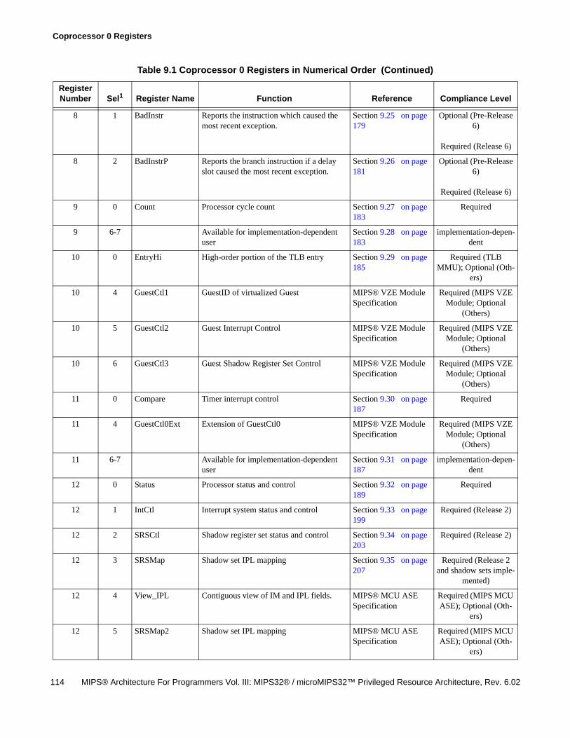
Coprocessor 0 Registers
114 MIPS® Architecture For Programmers Vol. III: MIPS32® / microMIPS32™ Privileged Resource Architecture, Rev. 6.02
8 1 BadInstr Reports the instruction which caused the most recent exception.
Section 9.25 on page 179
Optional (Pre-Release 6)
Required (Release 6)
8 2 BadInstrP Reports the branch instruction if a delay slot caused the most recent exception.
Section 9.26 on page 181
Optional (Pre-Release 6)
Required (Release 6)
9 0 Count Processor cycle count Section 9.27 on page 183
Required
9 6-7 Available for implementation-dependent user
Section 9.28 on page 183
implementation-depen-dent
10 0 EntryHi High-order portion of the TLB entry Section 9.29 on page 185
Required (TLB MMU); Optional (Oth-
ers)
10 4 GuestCtl1 GuestID of virtualized Guest MIPS® VZE Module Specification
Required (MIPS VZE Module; Optional
(Others)
10 5 GuestCtl2 Guest Interrupt Control MIPS® VZE Module Specification
Required (MIPS VZE Module; Optional
(Others)
10 6 GuestCtl3 Guest Shadow Register Set Control MIPS® VZE Module Specification
Required (MIPS VZE Module; Optional
(Others)
11 0 Compare Timer interrupt control Section 9.30 on page 187
Required
11 4 GuestCtl0Ext Extension of GuestCtl0 MIPS® VZE Module Specification
Required (MIPS VZE Module; Optional
(Others)
11 6-7 Available for implementation-dependent user
Section 9.31 on page 187
implementation-depen-dent
12 0 Status Processor status and control Section 9.32 on page 189
Required
12 1 IntCtl Interrupt system status and control Section 9.33 on page 199
Required (Release 2)
12 2 SRSCtl Shadow register set status and control Section 9.34 on page 203
Required (Release 2)
12 3 SRSMap Shadow set IPL mapping Section 9.35 on page 207
Required (Release 2 and shadow sets imple-
mented)
12 4 View_IPL Contiguous view of IM and IPL fields. MIPS® MCU ASE Specification
Required (MIPS MCU ASE); Optional (Oth-
ers)
12 5 SRSMap2 Shadow set IPL mapping MIPS® MCU ASE Specification
Required (MIPS MCU ASE); Optional (Oth-
ers)
Table 9.1 Coprocessor 0 Registers in Numerical Order (Continued)
Register Number Sel1 Register Name Function Reference Compliance Level
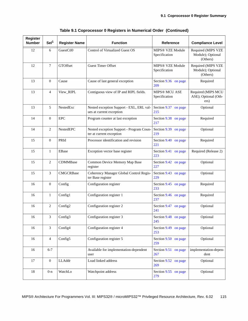
9.1 Coprocessor 0 Register Summary
MIPS® Architecture For Programmers Vol. III: MIPS32® / microMIPS32™ Privileged Resource Architecture, Rev. 6.02 115
12 6 GuestCtl0 Control of Virtualized Guest OS MIPS® VZE Module Specification
Required (MIPS VZE Module); Optional
(Others)
12 7 GTOffset Guest Timer Offset MIPS® VZE Module Specification
Required (MIPS VZE Module); Optional
(Others)
13 0 Cause Cause of last general exception Section 9.36 on page 209
Required
13 4 View_RIPL Contiguous view of IP and RIPL fields. MIPS® MCU ASE Specification
Required (MIPS MCU ASE); Optional (Oth-
ers)
13 5 NestedExc Nested exception Support - EXL, ERL val-ues at current exception
Section 9.37 on page 215
Optional
14 0 EPC Program counter at last exception Section 9.38 on page 217
Required
14 2 NestedEPC Nested exception Support - Program Coun-ter at current exception
Section 9.39 on page 219
Optional
15 0 PRId Processor identification and revision Section 9.40 on page 221
Required
15 1 EBase Exception vector base register Section 9.41 on page 223
Required (Release 2)
15 2 CDMMBase Common Device Memory Map Base register
Section 9.42 on page 227
Optional
15 3 CMGCRBase Coherency Manager Global Control Regis-ter Base register
Section 9.43 on page 229
Optional
16 0 Config Configuration register Section 9.45 on page 233
Required
16 1 Config1 Configuration register 1 Section 9.46 on page 237
Required
16 2 Config2 Configuration register 2 Section 9.47 on page 241
Optional
16 3 Config3 Configuration register 3 Section 9.48 on page 245
Optional
16 3 Config4 Configuration register 4 Section 9.49 on page 253
Optional
16 4 Config5 Configuration register 5 Section 9.50 on page 259
Optional
16 6-7 Available for implementation-dependent user
Section 9.51 on page 267
implementation-depen-dent
17 0 LLAddr Load linked address Section 9.52 on page 269
Optional
18 0-n WatchLo Watchpoint address Section 9.55 on page 279
Optional
Table 9.1 Coprocessor 0 Registers in Numerical Order (Continued)
Register Number Sel1 Register Name Function Reference Compliance Level
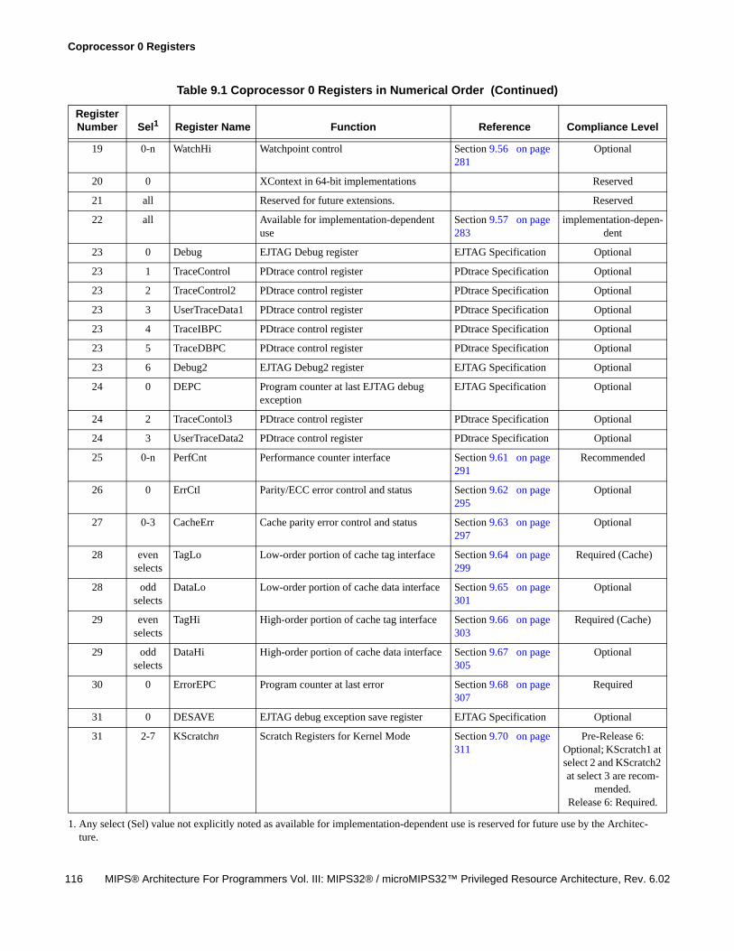
Coprocessor 0 Registers
116 MIPS® Architecture For Programmers Vol. III: MIPS32® / microMIPS32™ Privileged Resource Architecture, Rev. 6.02
19 0-n WatchHi Watchpoint control Section 9.56 on page 281
Optional
20 0 XContext in 64-bit implementations Reserved
21 all Reserved for future extensions. Reserved
22 all Available for implementation-dependent use
Section 9.57 on page 283
implementation-depen-dent
23 0 Debug EJTAG Debug register EJTAG Specification Optional
23 1 TraceControl PDtrace control register PDtrace Specification Optional
23 2 TraceControl2 PDtrace control register PDtrace Specification Optional
23 3 UserTraceData1 PDtrace control register PDtrace Specification Optional
23 4 TraceIBPC PDtrace control register PDtrace Specification Optional
23 5 TraceDBPC PDtrace control register PDtrace Specification Optional
23 6 Debug2 EJTAG Debug2 register EJTAG Specification Optional
24 0 DEPC Program counter at last EJTAG debug exception
EJTAG Specification Optional
24 2 TraceContol3 PDtrace control register PDtrace Specification Optional
24 3 UserTraceData2 PDtrace control register PDtrace Specification Optional
25 0-n PerfCnt Performance counter interface Section 9.61 on page 291
Recommended
26 0 ErrCtl Parity/ECC error control and status Section 9.62 on page 295
Optional
27 0-3 CacheErr Cache parity error control and status Section 9.63 on page 297
Optional
28 even selects
TagLo Low-order portion of cache tag interface Section 9.64 on page 299
Required (Cache)
28 odd selects
DataLo Low-order portion of cache data interface Section 9.65 on page 301
Optional
29 even selects
TagHi High-order portion of cache tag interface Section 9.66 on page 303
Required (Cache)
29 odd selects
DataHi High-order portion of cache data interface Section 9.67 on page 305
Optional
30 0 ErrorEPC Program counter at last error Section 9.68 on page 307
Required
31 0 DESAVE EJTAG debug exception save register EJTAG Specification Optional
31 2-7 KScratchn Scratch Registers for Kernel Mode Section 9.70 on page 311
Pre-Release 6: Optional; KScratch1 at select 2 and KScratch2 at select 3 are recom-
mended. Release 6: Required.
1. Any select (Sel) value not explicitly noted as available for implementation-dependent use is reserved for future use by the Architec-ture.
Table 9.1 Coprocessor 0 Registers in Numerical Order (Continued)
Register Number Sel1 Register Name Function Reference Compliance Level
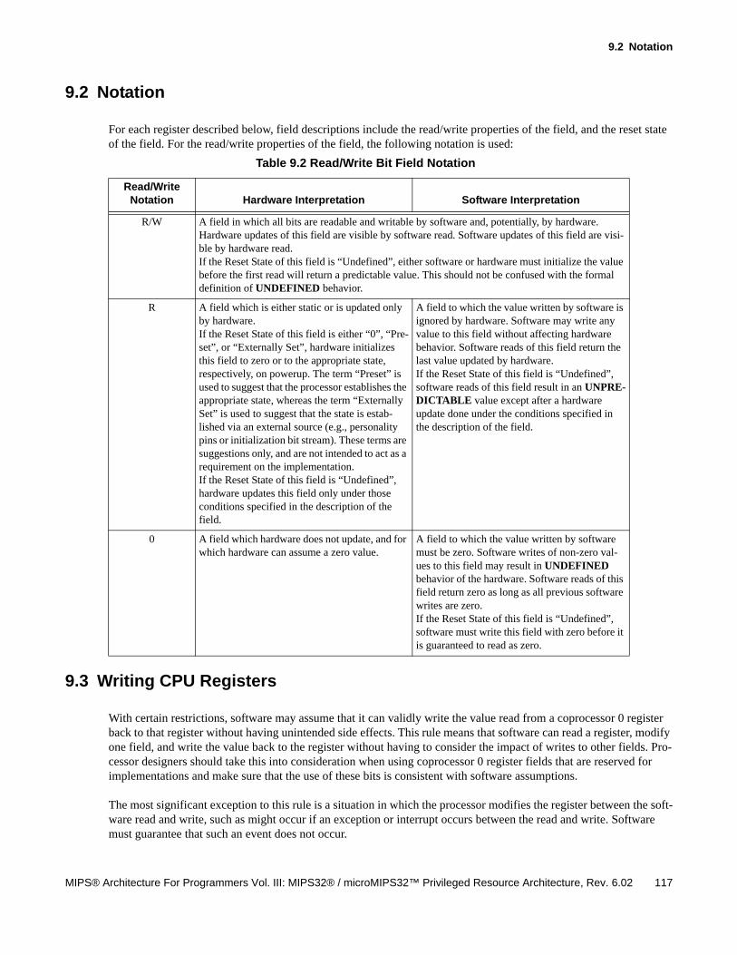
9.2 Notation
MIPS® Architecture For Programmers Vol. III: MIPS32® / microMIPS32™ Privileged Resource Architecture, Rev. 6.02 117
9.2 Notation
For each register described below, field descriptions include the read/write properties of the field, and the reset state of the field. For the read/write properties of the field, the following notation is used:
9.3 Writing CPU Registers
With certain restrictions, software may assume that it can validly write the value read from a coprocessor 0 register back to that register without having unintended side effects. This rule means that software can read a register, modify one field, and write the value back to the register without having to consider the impact of writes to other fields. Pro-cessor designers should take this into consideration when using coprocessor 0 register fields that are reserved for implementations and make sure that the use of these bits is consistent with software assumptions.
The most significant exception to this rule is a situation in which the processor modifies the register between the soft-ware read and write, such as might occur if an exception or interrupt occurs between the read and write. Software must guarantee that such an event does not occur.
Table 9.2 Read/Write Bit Field Notation
Read/Write Notation Hardware Interpretation Software Interpretation
R/W A field in which all bits are readable and writable by software and, potentially, by hardware.Hardware updates of this field are visible by software read. Software updates of this field are visi-ble by hardware read.If the Reset State of this field is “Undefined”, either software or hardware must initialize the value before the first read will return a predictable value. This should not be confused with the formal definition of UNDEFINED behavior.
R A field which is either static or is updated only by hardware.If the Reset State of this field is either “0”, “Pre-set”, or “Externally Set”, hardware initializes this field to zero or to the appropriate state, respectively, on powerup. The term “Preset” is used to suggest that the processor establishes the appropriate state, whereas the term “Externally Set” is used to suggest that the state is estab-lished via an external source (e.g., personality pins or initialization bit stream). These terms are suggestions only, and are not intended to act as a requirement on the implementation.If the Reset State of this field is “Undefined”, hardware updates this field only under those conditions specified in the description of the field.
A field to which the value written by software is ignored by hardware. Software may write any value to this field without affecting hardware behavior. Software reads of this field return the last value updated by hardware.If the Reset State of this field is “Undefined”, software reads of this field result in an UNPRE-DICTABLE value except after a hardware update done under the conditions specified in the description of the field.
0 A field which hardware does not update, and for which hardware can assume a zero value.
A field to which the value written by software must be zero. Software writes of non-zero val-ues to this field may result in UNDEFINED behavior of the hardware. Software reads of this field return zero as long as all previous software writes are zero.If the Reset State of this field is “Undefined”, software must write this field with zero before it is guaranteed to read as zero.
Coprocessor 0 Registers
118 MIPS® Architecture For Programmers Vol. III: MIPS32® / microMIPS32™ Privileged Resource Architecture, Rev. 6.02
Release 6 limits the number of cases where software can cause UNDEFINED or UNPREDICTABLE behavior. For example, in Release 6, for writes to a defined COP0 register field that may have reserved encodings, writes of unsup-ported values cause the write to be ignored by hardware. This means that no field in the COP0 register is modified unless all fields meet the conditions for writing. An exception to this rule is that if a field is reserved, then a write of a non-zero value to the reserved field is ignored but by itself does not cause the entire write to be dropped.
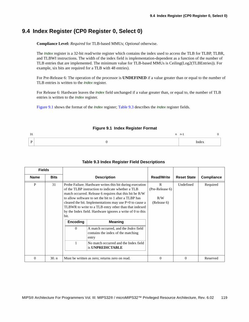
9.4 Index Register (CP0 Register 0, Select 0)
MIPS® Architecture For Programmers Vol. III: MIPS32® / microMIPS32™ Privileged Resource Architecture, Rev. 6.02 119
9.4 Index Register (CP0 Register 0, Select 0)
Compliance Level: Required for TLB-based MMUs; Optional otherwise.
The Index register is a 32-bit read/write register which contains the index used to access the TLB for TLBP, TLBR, and TLBWI instructions. The width of the index field is implementation-dependent as a function of the number of TLB entries that are implemented. The minimum value for TLB-based MMUs is Ceiling(Log2(TLBEntries)). For example, six bits are required for a TLB with 48 entries).
For Pre-Release 6: The operation of the processor is UNDEFINED if a value greater than or equal to the number of TLB entries is written to the Index register.
For Release 6: Hardware leaves the Index field unchanged if a value greater than, or equal to, the number of TLB entries is written to the Index register.
Figure 9.1 shows the format of the Index register; Table 9.3 describes the Index register fields.
Figure 9.1 Index Register Format
31 n n-1 0
P 0 Index
Table 9.3 Index Register Field Descriptions
Fields
Description Read/Write Reset State ComplianceName Bits
P 31 Probe Failure. Hardware writes this bit during execution of the TLBP instruction to indicate whether a TLB match occurred. Release 6 requires that this bit be R/W to allow software to set the bit to 1 after a TLBP has cleared the bit. Implementations may use P=0 to cause a TLBWR to write to a TLB entry other than that indexed by the Index field. Hardware ignores a write of 0 to this bit.
R(Pre-Release 6)
R/W(Release 6)
Undefined Required
0 30. n Must be written as zero; returns zero on read. 0 0 Reserved
Encoding Meaning
0 A match occurred, and the Index field contains the index of the matching entry
1 No match occurred and the Index field is UNPREDICTABLE
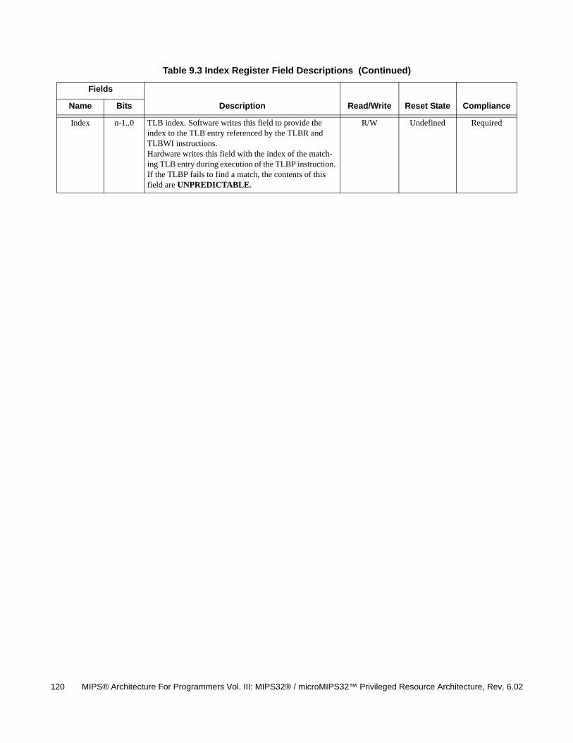
120 MIPS® Architecture For Programmers Vol. III: MIPS32® / microMIPS32™ Privileged Resource Architecture, Rev. 6.02
Index n-1..0 TLB index. Software writes this field to provide the index to the TLB entry referenced by the TLBR and TLBWI instructions.Hardware writes this field with the index of the match-ing TLB entry during execution of the TLBP instruction. If the TLBP fails to find a match, the contents of this field are UNPREDICTABLE.
R/W Undefined Required
Table 9.3 Index Register Field Descriptions (Continued)
Fields
Description Read/Write Reset State ComplianceName Bits
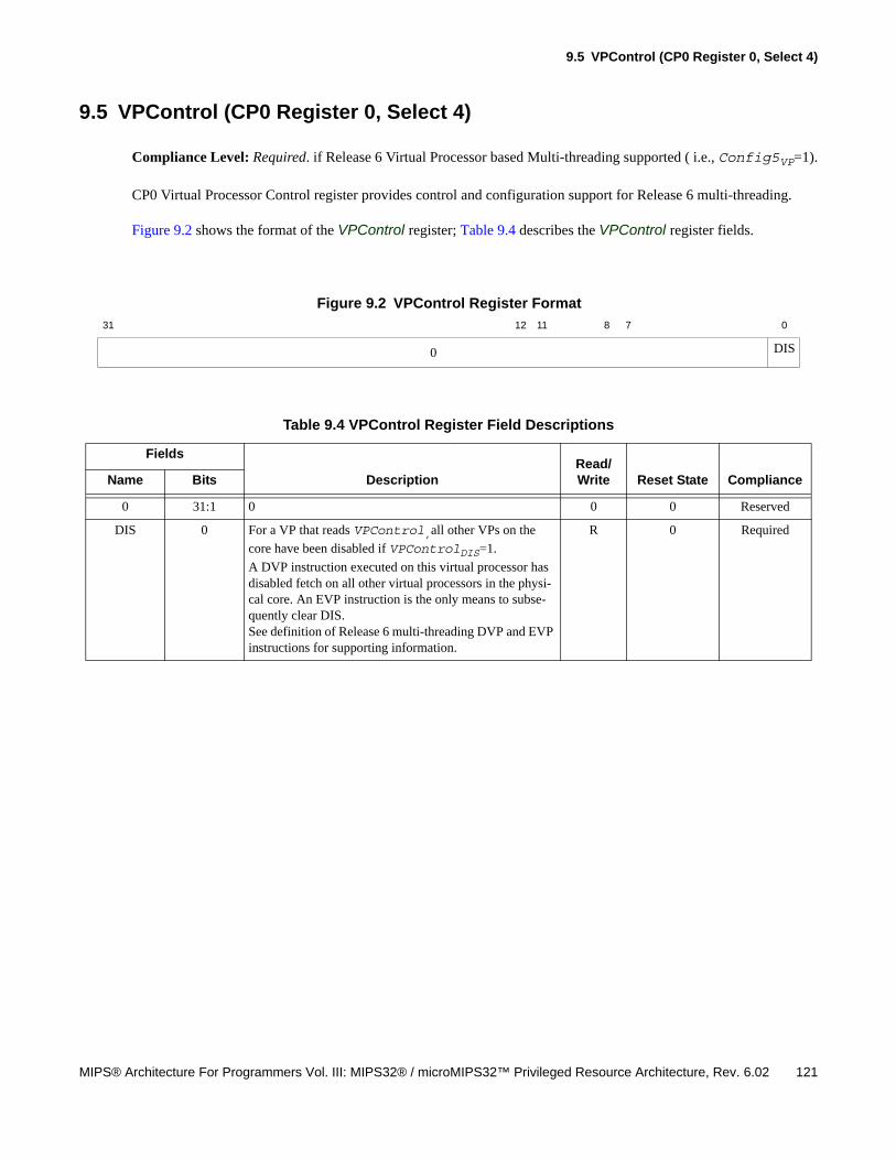
9.5 VPControl (CP0 Register 0, Select 4)
MIPS® Architecture For Programmers Vol. III: MIPS32® / microMIPS32™ Privileged Resource Architecture, Rev. 6.02 121
9.5 VPControl (CP0 Register 0, Select 4)
Compliance Level: Required. if Release 6 Virtual Processor based Multi-threading supported ( i.e., Config5VP=1).
CP0 Virtual Processor Control register provides control and configuration support for Release 6 multi-threading.
Figure 9.2 shows the format of the VPControl register; Table 9.4 describes the VPControl register fields.
Figure 9.2 VPControl Register Format
31 12 11 8 7 0
0 DIS
Table 9.4 VPControl Register Field Descriptions
Fields
DescriptionRead/Write Reset State ComplianceName Bits
0 31:1 0 0 0 Reserved
DIS 0 For a VP that reads VPControl,all other VPs on the
core have been disabled if VPControlDIS=1.
A DVP instruction executed on this virtual processor has disabled fetch on all other virtual processors in the physi-cal core. An EVP instruction is the only means to subse-quently clear DIS.See definition of Release 6 multi-threading DVP and EVP instructions for supporting information.
R 0 Required

122 MIPS® Architecture For Programmers Vol. III: MIPS32® / microMIPS32™ Privileged Resource Architecture, Rev. 6.02
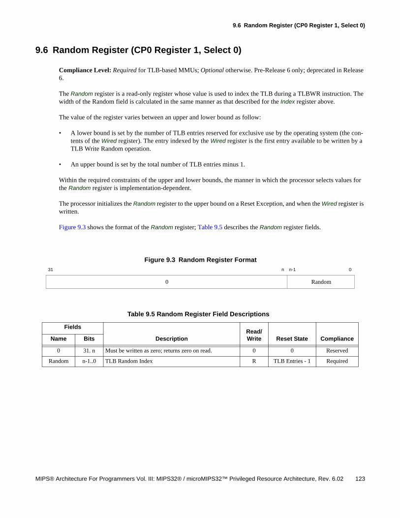
9.6 Random Register (CP0 Register 1, Select 0)
MIPS® Architecture For Programmers Vol. III: MIPS32® / microMIPS32™ Privileged Resource Architecture, Rev. 6.02 123
9.6 Random Register (CP0 Register 1, Select 0)
Compliance Level: Required for TLB-based MMUs; Optional otherwise. Pre-Release 6 only; deprecated in Release 6.
The Random register is a read-only register whose value is used to index the TLB during a TLBWR instruction. The width of the Random field is calculated in the same manner as that described for the Index register above.
The value of the register varies between an upper and lower bound as follow:
• A lower bound is set by the number of TLB entries reserved for exclusive use by the operating system (the con-tents of the Wired register). The entry indexed by the Wired register is the first entry available to be written by a TLB Write Random operation.
• An upper bound is set by the total number of TLB entries minus 1.
Within the required constraints of the upper and lower bounds, the manner in which the processor selects values for the Random register is implementation-dependent.
The processor initializes the Random register to the upper bound on a Reset Exception, and when the Wired register is written.
Figure 9.3 shows the format of the Random register; Table 9.5 describes the Random register fields.
Figure 9.3 Random Register Format
31 n n-1 0
0 Random
Table 9.5 Random Register Field Descriptions
Fields
DescriptionRead/Write Reset State ComplianceName Bits
0 31. n Must be written as zero; returns zero on read. 0 0 Reserved
Random n-1..0 TLB Random Index R TLB Entries - 1 Required

124 MIPS® Architecture For Programmers Vol. III: MIPS32® / microMIPS32™ Privileged Resource Architecture, Rev. 6.02
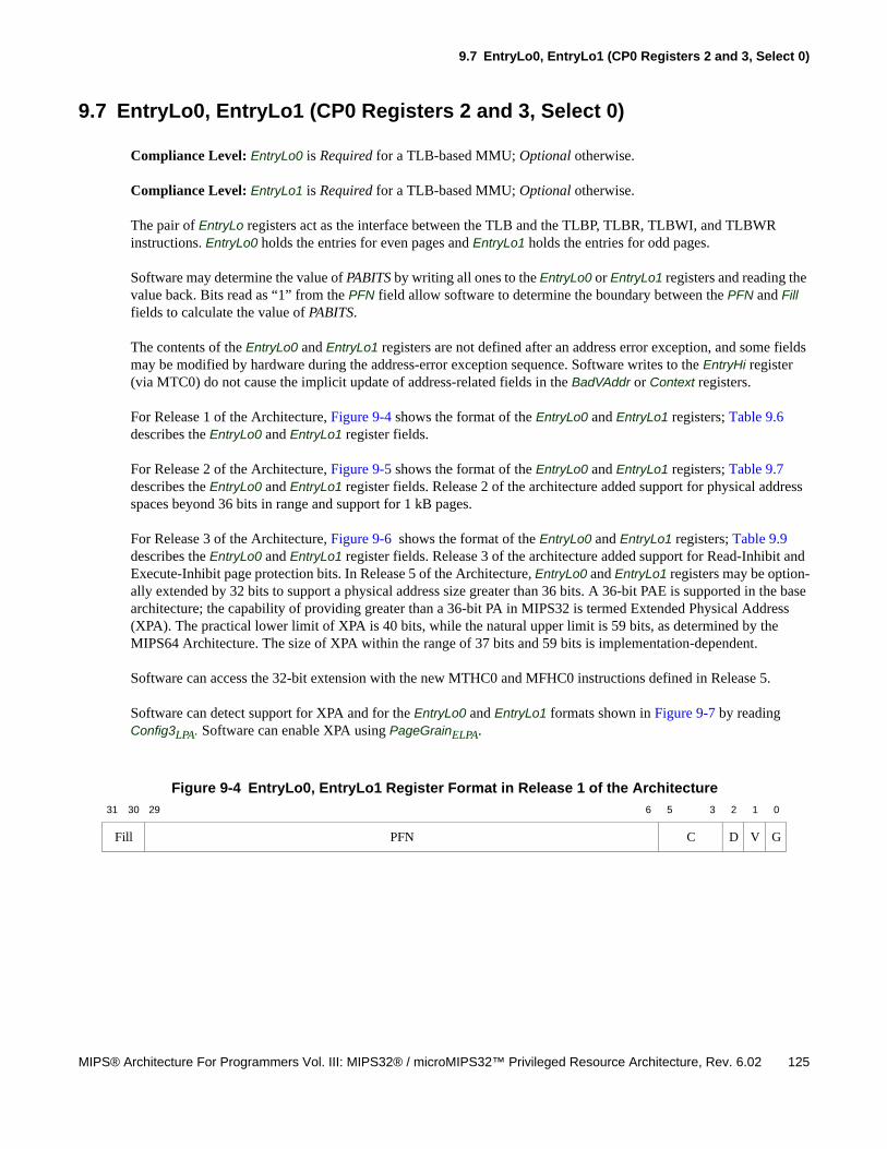
9.7 EntryLo0, EntryLo1 (CP0 Registers 2 and 3, Select 0)
MIPS® Architecture For Programmers Vol. III: MIPS32® / microMIPS32™ Privileged Resource Architecture, Rev. 6.02 125
9.7 EntryLo0, EntryLo1 (CP0 Registers 2 and 3, Select 0)
Compliance Level: EntryLo0 is Required for a TLB-based MMU; Optional otherwise.
Compliance Level: EntryLo1 is Required for a TLB-based MMU; Optional otherwise.
The pair of EntryLo registers act as the interface between the TLB and the TLBP, TLBR, TLBWI, and TLBWR instructions. EntryLo0 holds the entries for even pages and EntryLo1 holds the entries for odd pages.
Software may determine the value of PABITS by writing all ones to the EntryLo0 or EntryLo1 registers and reading the value back. Bits read as “1” from the PFN field allow software to determine the boundary between the PFN and Fill fields to calculate the value of PABITS.
The contents of the EntryLo0 and EntryLo1 registers are not defined after an address error exception, and some fields may be modified by hardware during the address-error exception sequence. Software writes to the EntryHi register (via MTC0) do not cause the implicit update of address-related fields in the BadVAddr or Context registers.
For Release 1 of the Architecture, Figure 9-4 shows the format of the EntryLo0 and EntryLo1 registers; Table 9.6 describes the EntryLo0 and EntryLo1 register fields.
For Release 2 of the Architecture, Figure 9-5 shows the format of the EntryLo0 and EntryLo1 registers; Table 9.7 describes the EntryLo0 and EntryLo1 register fields. Release 2 of the architecture added support for physical address spaces beyond 36 bits in range and support for 1 kB pages.
For Release 3 of the Architecture, Figure 9-6 shows the format of the EntryLo0 and EntryLo1 registers; Table 9.9 describes the EntryLo0 and EntryLo1 register fields. Release 3 of the architecture added support for Read-Inhibit and Execute-Inhibit page protection bits. In Release 5 of the Architecture, EntryLo0 and EntryLo1 registers may be option-ally extended by 32 bits to support a physical address size greater than 36 bits. A 36-bit PAE is supported in the base architecture; the capability of providing greater than a 36-bit PA in MIPS32 is termed Extended Physical Address (XPA). The practical lower limit of XPA is 40 bits, while the natural upper limit is 59 bits, as determined by the MIPS64 Architecture. The size of XPA within the range of 37 bits and 59 bits is implementation-dependent.
Software can access the 32-bit extension with the new MTHC0 and MFHC0 instructions defined in Release 5.
Software can detect support for XPA and for the EntryLo0 and EntryLo1 formats shown in Figure 9-7 by reading Config3LPA. Software can enable XPA using PageGrainELPA.
Figure 9-4 EntryLo0, EntryLo1 Register Format in Release 1 of the Architecture
31 30 29 6 5 3 2 1 0
Fill PFN C D V G
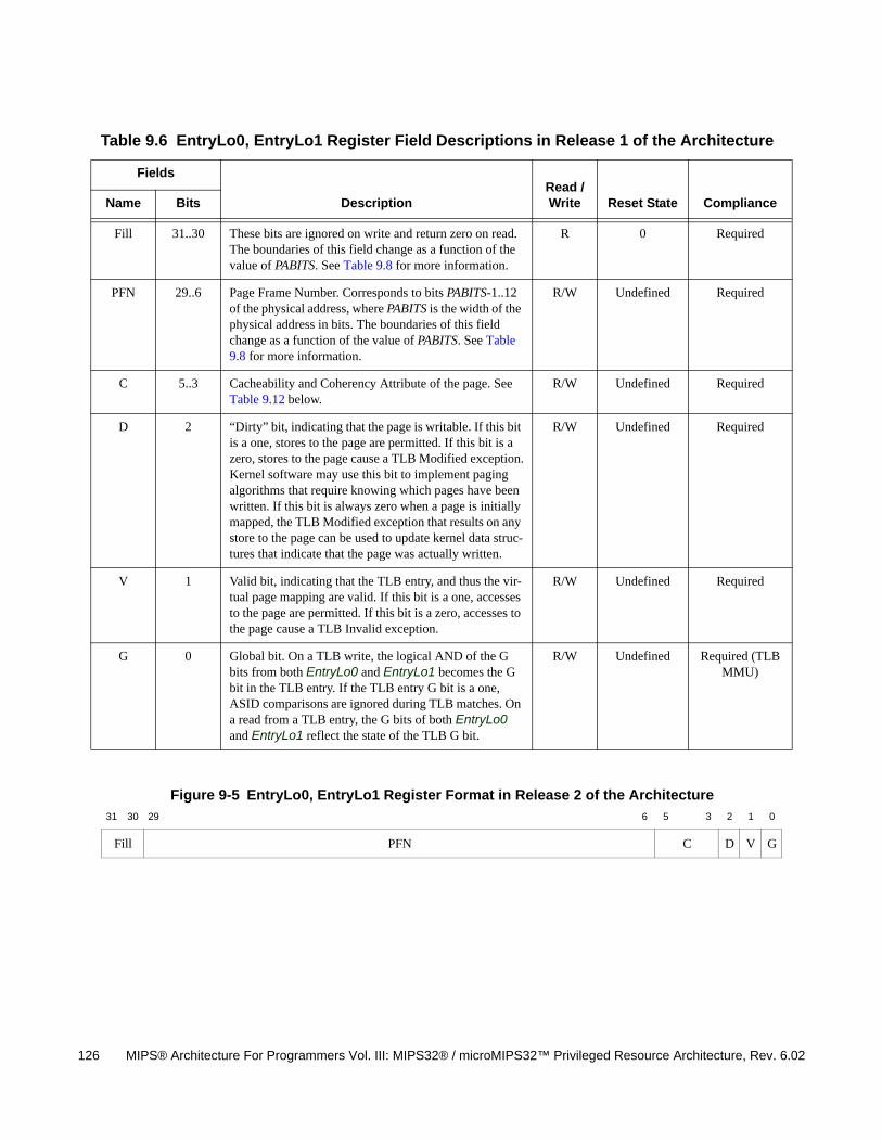
126 MIPS® Architecture For Programmers Vol. III: MIPS32® / microMIPS32™ Privileged Resource Architecture, Rev. 6.02
Table 9.6 EntryLo0, EntryLo1 Register Field Descriptions in Release 1 of the Architecture
Fields
DescriptionRead / Write Reset State ComplianceName Bits
Fill 31..30 These bits are ignored on write and return zero on read. The boundaries of this field change as a function of the value of PABITS. See Table 9.8 for more information.
R 0 Required
PFN 29..6 Page Frame Number. Corresponds to bits PABITS-1..12 of the physical address, where PABITS is the width of the physical address in bits. The boundaries of this field change as a function of the value of PABITS. See Table 9.8 for more information.
R/W Undefined Required
C 5..3 Cacheability and Coherency Attribute of the page. See Table 9.12 below.
R/W Undefined Required
D 2 “Dirty” bit, indicating that the page is writable. If this bit is a one, stores to the page are permitted. If this bit is a zero, stores to the page cause a TLB Modified exception.Kernel software may use this bit to implement paging algorithms that require knowing which pages have been written. If this bit is always zero when a page is initially mapped, the TLB Modified exception that results on any store to the page can be used to update kernel data struc-tures that indicate that the page was actually written.
R/W Undefined Required
V 1 Valid bit, indicating that the TLB entry, and thus the vir-tual page mapping are valid. If this bit is a one, accesses to the page are permitted. If this bit is a zero, accesses to the page cause a TLB Invalid exception.
R/W Undefined Required
G 0 Global bit. On a TLB write, the logical AND of the G bits from both EntryLo0 and EntryLo1 becomes the G bit in the TLB entry. If the TLB entry G bit is a one, ASID comparisons are ignored during TLB matches. On a read from a TLB entry, the G bits of both EntryLo0 and EntryLo1 reflect the state of the TLB G bit.
R/W Undefined Required (TLB MMU)
Figure 9-5 EntryLo0, EntryLo1 Register Format in Release 2 of the Architecture
31 30 29 6 5 3 2 1 0
Fill PFN C D V G
9.7 EntryLo0, EntryLo1 (CP0 Registers 2 and 3, Select 0)
MIPS® Architecture For Programmers Vol. III: MIPS32® / microMIPS32™ Privileged Resource Architecture, Rev. 6.02 127
Table 9.8 shows the movement of the Fill and PFN fields as a function of 1 kB page support enabled, and the value of PABITS. Note that in implementations of Release 1 of the Architecture, there is no support for 1 kB pages, so only the first row of the table applies to Release 1.
Table 9.7 EntryLo0, EntryLo1 Register Field Descriptions in Release 2 of the Architecture
Fields
DescriptionRead / Write Reset State ComplianceName Bits
Fill 31..30 These bits are ignored on write and return zero on read. The boundaries of this field change as a function of the value of PABITS. See Table 9.8 for more information.
R 0 Required
PFN 29..6 Page Frame Number. This field contains the physical page number corresponding to the virtual page.If the processor is enabled to support 1 kB pages (Config3SP = 1 and PageGrainESP = 1), the PFN field
corresponds to bits 33..10 of the physical address (the field is shifted left by 2 bits relative to the Release 1 def-inition to make room for PA11 10).
If the processor is not enabled to support 1 kB pages (Config3SP = 0 or PageGrainESP = 0), the PFN field
corresponds to bits 35..12 of the physical address.The boundaries of this field change as a function of the value of PABITS. See Table 9.8 for more information.
R/W Undefined Required
C 5..3 The definition of this field is unchanged from Release 1. See Table 9.6 above and Table 9.12 below.
R/W Undefined Required
D 2 The definition of this field is unchanged from Release 1. See Table 9.6 above.
R/W Undefined Required
V 1 The definition of this field is unchanged from Release 1. See Table 9.6 above.
R/W Undefined Required
G 0 The definition of this field is unchanged from Release 1. See Table 9.6 above.
R/W Undefined Required (TLB MMU)
Table 9.8 EntryLo Field Widths as a Function of PABITS
1 kB Page
Support Enabled? PABITS Value
Corresponding EntryLo Field Bit Ranges
Release 2 Required?Fill Field PFN Field
No 36 PABITS > 12 31..(30-(36-PABITS))Example:
31..30 if PABITS = 3631..7 if PABITS = 13
(29-(36-PABITS))..6Example:
29..6 if PABITS = 366..6 if PABITS = 13
EntryLo29 6 = PA35 12
No
128 MIPS® Architecture For Programmers Vol. III: MIPS32® / microMIPS32™ Privileged Resource Architecture, Rev. 6.02
Yes 34 PABITS > 10 31..(30-(34-PABITS))Example:
31..30 if PABITS = 3431..7 if PABITS = 11
(29-(34-PABITS))..6Example:
29..6 if PABITS = 346..6 if PABITS = 11
EntryLo29 6 = PA33 10
Yes
Figure 9-6 EntryLo0, EntryLo1 Register Format in Release 3 of the Architecture
31 30 29 6 5 3 2 1 0
RI XI PFN C D V G
Table 9.9 EntryLo0, EntryLo1 Register Field Descriptions in Release 3 of the Architecture
Fields
DescriptionRead / Write Reset State ComplianceName Bits
Fill 31..30 These bits are ignored on write and return zero on read. The boundaries of this field change as a function of the value of PABITS. See Table 9.8 for more information.
R 0 Required if RI and XI fields are
not imple-mented.
RI 31 Read Inhibit. If this bit is set in a TLB entry, an attempt, other than a MIPS16 PC-relative load, to read data on the virtual page causes a TLB Invalid or a TLBRI excep-tion, even if the V (Valid) bit is set. The RI bit is writable only if the RIE bit of the PageGrain register is set. If the RIE bit of PageGrain is not set, the RI bit of EntryLo0/EntryLo1 is set to zero on any write to the register, regardless of the value written.
This bit is optional and its existence is denoted by the Config3RXI or Config3SM register fields.
R/W 0 Required by SmartMIPS
ASE; Optional otherwise
If not imple-mented, this bit location is part of the Fill field.
Table 9.8 EntryLo Field Widths as a Function of PABITS (Continued)
1 kB Page
Support Enabled? PABITS Value
Corresponding EntryLo Field Bit Ranges
Release 2 Required?Fill Field PFN Field
9.7 EntryLo0, EntryLo1 (CP0 Registers 2 and 3, Select 0)
MIPS® Architecture For Programmers Vol. III: MIPS32® / microMIPS32™ Privileged Resource Architecture, Rev. 6.02 129
Figure 9-7 applies to Table 9.10, specifically to MIPS32 support for XPA (PA > 36 bits), and it shows the natural upper limit of XPA. If only 40-bit XPA is supported, the most-significant bit of PFNX is EntryLo0[35] and EntryLo1[35].
XI 30 Execute Inhibit. If this bit is set in a TLB entry, an attempt to fetch an instruction or to load MIPS16 PC-rel-ative data from the virtual page causes a TLB Invalid or a TLBXI exception, even if the V (Valid) bit is set. The XI bit is writable only if the XIE bit of the PageGrain register is set. If the XIE bit of PageGrain is not set, the XI bit of EntryLo0/EntryLo1 is set to zero on any write to the register, regardless of the value written.
This bit is optional and its existence is denoted by the Config3RXI or Config3SM register fields.
R/W 0 Required by SmartMIPS
ASE; Optionalotherwise
If not imple-mented, this bit location is part of the Fill field.
PFN 29..6 Page Frame Number. This field contains the physical page number corresponding to the virtual page.If the processor is enabled to support 1 kB pages (Config3SP = 1 and PageGrainESP = 1), the PFN field
corresponds to bits 33..10 of the physical address (the field is shifted left by 2 bits relative to the Release 1 def-inition to make room for PA11 10).
If the processor is not enabled to support 1 kB pages (Config3SP = 0 or PageGrainESP = 0), the PFN field
corresponds to bits 35..12 of the physical address.The boundaries of this field change as a function of the value of PABITS. See Table 9.8 for more information.
R/W Undefined Required
C 5..3 The definition of this field is unchanged from Release 1. See Table 9.6 above and Table 9.12 below.
R/W Undefined Required
D 2 The definition of this field is unchanged from Release 1. See Table 9.6 above.
R/W Undefined Required
V 1 The definition of this field is unchanged from Release 1. See Table 9.6 above.
R/W Undefined Required
G 0 The definition of this field is unchanged from Release 1. See Table 9.6 above.
R/W Undefined Required (TLB MMU)
Figure 9-7 EntryLo0, EntryLo1 Register Format in Release 5
63 55 54 36 35 32
Fill PFNX
RI XI PFN C D V G
31 30 29 6 5 3 2 1 0
Table 9.9 EntryLo0, EntryLo1 Register Field Descriptions in Release 3 of the Architecture
Fields
DescriptionRead / Write Reset State ComplianceName Bits
130 MIPS® Architecture For Programmers Vol. III: MIPS32® / microMIPS32™ Privileged Resource Architecture, Rev. 6.02
Table 9.10 EntryLo0, EntryLo1 Register Field Descriptions in Release 5 of the Architecture
Fields
DescriptionRead / Write Reset State ComplianceName Bits
Fill 63..55 These bits are ignored on write and return zero on read. The boundaries of this field change as a function of the value of PABITS.
R 0 Required for XPA; Optional
otherwise
PFNX 54..32 Page Frame Number Extension. If the processor is enabled to support XPA (Config3LPA =1 and
PageGrainELPA =1) this field is concatenated with the
PFN field to form the full page frame number corre-sponding to the physical address, thereby providing up to 59 bits of physical address.If the processor is enabled to support 1 kB pages (Config3SP = 1 and PageGrainESP =1), the combined
PFNX PFN fields corresponds to bits PABITS-1..10 of the physical address (the field is shifted left by 2 bits rel-ative to the Release 1 definition to make room for PA11 10).
If the processor is not enabled to support 1 kB pages (Config3SP = 0 or PageGrainESP = 0), the combined
PFNX PFN fields corresponds to 0b00 bits PABITS-1..12 of the physical address (the field is unshifted and the upper two bits must be written as zero).The boundaries of this field change as a function of the value of PABITS. See Table 9.11 for more information.If support for large physical addresses is not enabled (Config3LPA = 0 or PageGrainELPA = 0), these bits are
ignored on write and return 0 on read, thereby providing full backward compatibility with implementations of Release 1 of the Architecture.To ensure backward compatibility with pre-Release 5 software that does not support XPA, MTC0 is required to zero out the extension bits if Config5MVH=1.
R/W Undefined Required for XPA; Optional
otherwise
RI 31 Read Inhibit. If this bit is set in a TLB entry, an attempt, other than a MIPS16 PC-relative load, to read data on the virtual page causes a TLB Invalid or a TLBRI excep-tion, even if the V (Valid) bit is set. The RI bit is writable only if the RIE bit of the PageGrain register is set. If the RIE bit of PageGrain is not set, the RI bit of EntryLo0/EntryLo1 is set to zero on any write to the register, regardless of the value written.
This bit is optional and its existence is denoted by the Config3RXI or Config3SM register fields.
If not implemented, then reads of this field return 0.
R/W 0 Required by SmartMIPS
ASE; Optional otherwise
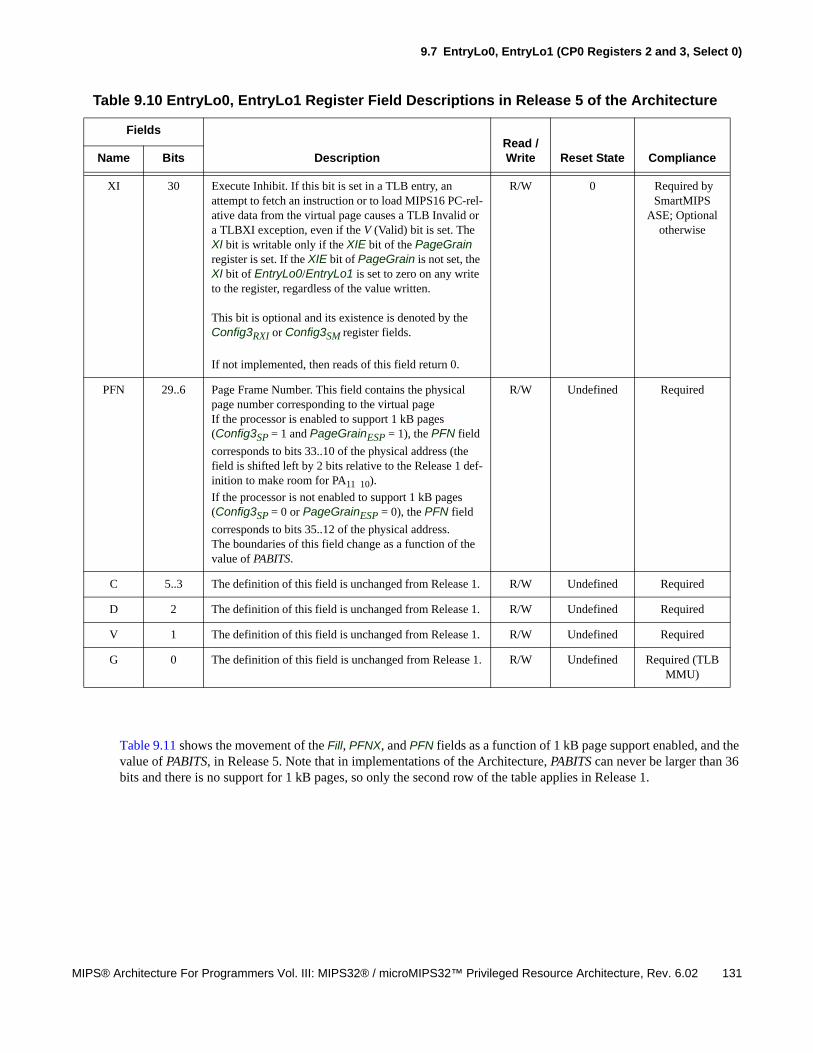
9.7 EntryLo0, EntryLo1 (CP0 Registers 2 and 3, Select 0)
MIPS® Architecture For Programmers Vol. III: MIPS32® / microMIPS32™ Privileged Resource Architecture, Rev. 6.02 131
Table 9.11 shows the movement of the Fill, PFNX, and PFN fields as a function of 1 kB page support enabled, and the value of PABITS, in Release 5. Note that in implementations of the Architecture, PABITS can never be larger than 36 bits and there is no support for 1 kB pages, so only the second row of the table applies in Release 1.
XI 30 Execute Inhibit. If this bit is set in a TLB entry, an attempt to fetch an instruction or to load MIPS16 PC-rel-ative data from the virtual page causes a TLB Invalid or a TLBXI exception, even if the V (Valid) bit is set. The XI bit is writable only if the XIE bit of the PageGrain register is set. If the XIE bit of PageGrain is not set, the XI bit of EntryLo0/EntryLo1 is set to zero on any write to the register, regardless of the value written.
This bit is optional and its existence is denoted by the Config3RXI or Config3SM register fields.
If not implemented, then reads of this field return 0.
R/W 0 Required by SmartMIPS
ASE; Optional otherwise
PFN 29..6 Page Frame Number. This field contains the physical page number corresponding to the virtual pageIf the processor is enabled to support 1 kB pages (Config3SP = 1 and PageGrainESP = 1), the PFN field
corresponds to bits 33..10 of the physical address (the field is shifted left by 2 bits relative to the Release 1 def-inition to make room for PA11 10).
If the processor is not enabled to support 1 kB pages (Config3SP = 0 or PageGrainESP = 0), the PFN field
corresponds to bits 35..12 of the physical address.The boundaries of this field change as a function of the value of PABITS.
R/W Undefined Required
C 5..3 The definition of this field is unchanged from Release 1. R/W Undefined Required
D 2 The definition of this field is unchanged from Release 1. R/W Undefined Required
V 1 The definition of this field is unchanged from Release 1. R/W Undefined Required
G 0 The definition of this field is unchanged from Release 1. R/W Undefined Required (TLB MMU)
Table 9.10 EntryLo0, EntryLo1 Register Field Descriptions in Release 5 of the Architecture
Fields
DescriptionRead / Write Reset State ComplianceName Bits
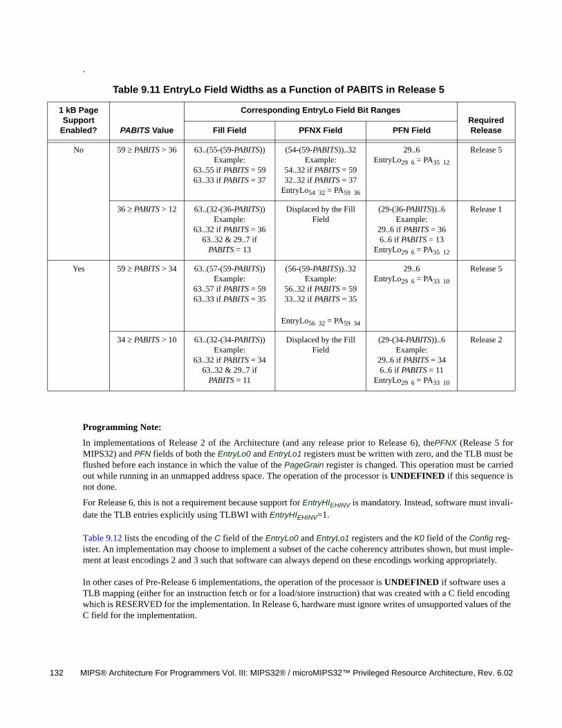
132 MIPS® Architecture For Programmers Vol. III: MIPS32® / microMIPS32™ Privileged Resource Architecture, Rev. 6.02
.
Programming Note:
In implementations of Release 2 of the Architecture (and any release prior to Release 6), thePFNX (Release 5 forMIPS32) and PFN fields of both the EntryLo0 and EntryLo1 registers must be written with zero, and the TLB must beflushed before each instance in which the value of the PageGrain register is changed. This operation must be carriedout while running in an unmapped address space. The operation of the processor is UNDEFINED if this sequence isnot done.
For Release 6, this is not a requirement because support for EntryHIEHINV is mandatory. Instead, software must invali-date the TLB entries explicitly using TLBWI with EntryHIEHINV=1.
Table 9.12 lists the encoding of the C field of the EntryLo0 and EntryLo1 registers and the K0 field of the Config reg-ister. An implementation may choose to implement a subset of the cache coherency attributes shown, but must imple-ment at least encodings 2 and 3 such that software can always depend on these encodings working appropriately.
In other cases of Pre-Release 6 implementations, the operation of the processor is UNDEFINED if software uses a TLB mapping (either for an instruction fetch or for a load/store instruction) that was created with a C field encoding which is RESERVED for the implementation. In Release 6, hardware must ignore writes of unsupported values of the C field for the implementation.
Table 9.11 EntryLo Field Widths as a Function of PABITS in Release 5
1 kB Page Support
Enabled? PABITS Value
Corresponding EntryLo Field Bit RangesRequiredRelease Fill Field PFNX Field PFN Field
No 59 PABITS > 36 63..(55-(59-PABITS))Example:
63..55 if PABITS = 5963..33 if PABITS = 37
(54-(59-PABITS))..32Example:
54..32 if PABITS = 5932..32 if PABITS = 37
EntryLo54 32 = PA59 36
29..6EntryLo29 6 = PA35 12
Release 5
36 PABITS > 12 63..(32-(36-PABITS))Example:
63..32 if PABITS = 3663..32 & 29..7 if
PABITS = 13
Displaced by the Fill Field
(29-(36-PABITS))..6Example:
29..6 if PABITS = 366..6 if PABITS = 13
EntryLo29 6 = PA35 12
Release 1
Yes 59 PABITS > 34 63..(57-(59-PABITS))Example:
63..57 if PABITS = 5963..33 if PABITS = 35
(56-(59-PABITS))..32Example:
56..32 if PABITS = 5933..32 if PABITS = 35
EntryLo56 32 = PA59 34
29..6EntryLo29 6 = PA33 10
Release 5
34 PABITS > 10 63..(32-(34-PABITS))Example:
63..32 if PABITS = 3463..32 & 29..7 if
PABITS = 11
Displaced by the Fill Field
(29-(34-PABITS))..6Example:
29..6 if PABITS = 346..6 if PABITS = 11
EntryLo29 6 = PA33 10
Release 2
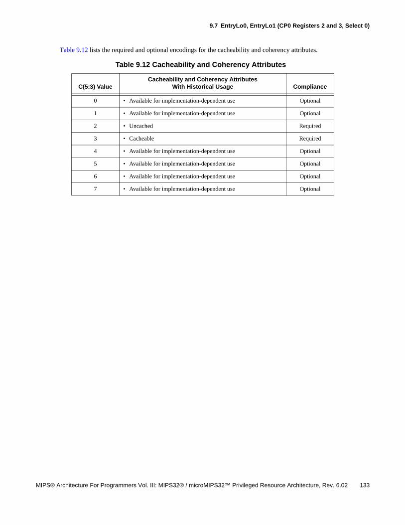
9.7 EntryLo0, EntryLo1 (CP0 Registers 2 and 3, Select 0)
MIPS® Architecture For Programmers Vol. III: MIPS32® / microMIPS32™ Privileged Resource Architecture, Rev. 6.02 133
Table 9.12 lists the required and optional encodings for the cacheability and coherency attributes.
Table 9.12 Cacheability and Coherency Attributes
C(5:3) ValueCacheability and Coherency Attributes
With Historical Usage Compliance
0 • Available for implementation-dependent use Optional
1 • Available for implementation-dependent use Optional
2 • Uncached Required
3 • Cacheable Required
4 • Available for implementation-dependent use Optional
5 • Available for implementation-dependent use Optional
6 • Available for implementation-dependent use Optional
7 • Available for implementation-dependent use Optional

134 MIPS® Architecture For Programmers Vol. III: MIPS32® / microMIPS32™ Privileged Resource Architecture, Rev. 6.02
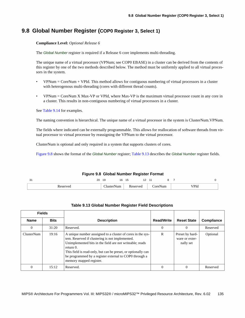
9.8 Global Number Register (COP0 Register 3, Select 1)
MIPS® Architecture For Programmers Vol. III: MIPS32® / microMIPS32™ Privileged Resource Architecture, Rev. 6.02 135
9.8 Global Number Register (COP0 Register 3, Select 1)
Compliance Level: Optional Release 6
The Global Number register is required if a Release 6 core implements multi-threading.
The unique name of a virtual processor (VPNum; see COP0 EBASE) in a cluster can be derived from the contents of this register by one of the two methods described below. The method must be uniformly applied to all virtual proces-sors in the system.
• VPNum = CoreNum + VPId. This method allows for contiguous numbering of virtual processors in a cluster with heterogenous multi-threading (cores with different thread counts).
• VPNum = CoreNum X Max-VP or VPId, where Max-VP is the maximum virtual processor count in any core in a cluster. This results in non-contiguous numbering of virtual processors in a cluster.
See Table 9.14 for examples.
The naming convention is hierarchical. The unique name of a virtual processor in the system is ClusterNum.VPNum.
The fields where indicated can be externally programmable. This allows for reallocation of software threads from vir-tual processor to virtual processor by reassigning the VPNum to the virtual processor.
ClusterNum is optional and only required in a system that supports clusters of cores.
Figure 9.8 shows the format of the Global Number register; Table 9.13 describes the Global Number register fields.
Figure 9.8 Global Number Register Format
31 20 19 16 15 12 11 8 7 0
Reserved ClusterNum Reserved CoreNum VPId
Table 9.13 Global Number Register Field Descriptions
Fields
Description Read/Write Reset State ComplianceName Bits
0 31:20 Reserved. 0 0 Reserved
ClusterNum 19:16 A unique number asssigned to a cluster of cores in the sys-tem. Reserved if clustering is not implemented.Unimplemented bits in the field are not writeable; reads return 0.This field is read-only, but can be preset, or optionally can be programmed by a register external to COP0 through a memory mapped register.
R Preset by hard-ware or exter-
nally set
Optional
0 15:12 Reserved. 0 0 Reserved
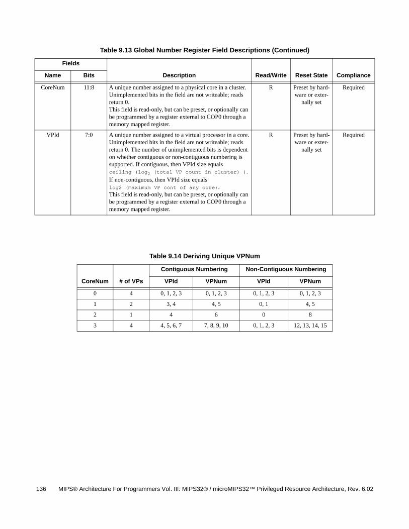
136 MIPS® Architecture For Programmers Vol. III: MIPS32® / microMIPS32™ Privileged Resource Architecture, Rev. 6.02
CoreNum 11:8 A unique number assigned to a physical core in a cluster.Unimplemented bits in the field are not writeable; reads return 0. This field is read-only, but can be preset, or optionally can be programmed by a register external to COP0 through a memory mapped register.
R Preset by hard-ware or exter-
nally set
Required
VPId 7:0 A unique number assigned to a virtual processor in a core.Unimplemented bits in the field are not writeable; reads return 0. The number of unimplemented bits is dependent on whether contiguous or non-contiguous numbering is supported. If contiguous, then VPId size equals ceiling (log2 (total VP count in cluster) ). If non-contiguous, then VPId size equals log2 (maximum VP cont of any core).This field is read-only, but can be preset, or optionally can be programmed by a register external to COP0 through a memory mapped register.
R Preset by hard-ware or exter-
nally set
Required
Table 9.14 Deriving Unique VPNum
CoreNum # of VPs
Contiguous Numbering Non-Contiguous Numbering
VPId VPNum VPId VPNum
0 4 0, 1, 2, 3 0, 1, 2, 3 0, 1, 2, 3 0, 1, 2, 3
1 2 3, 4 4, 5 0, 1 4, 5
2 1 4 6 0 8
3 4 4, 5, 6, 7 7, 8, 9, 10 0, 1, 2, 3 12, 13, 14, 15
Table 9.13 Global Number Register Field Descriptions (Continued)
Fields
Description Read/Write Reset State ComplianceName Bits
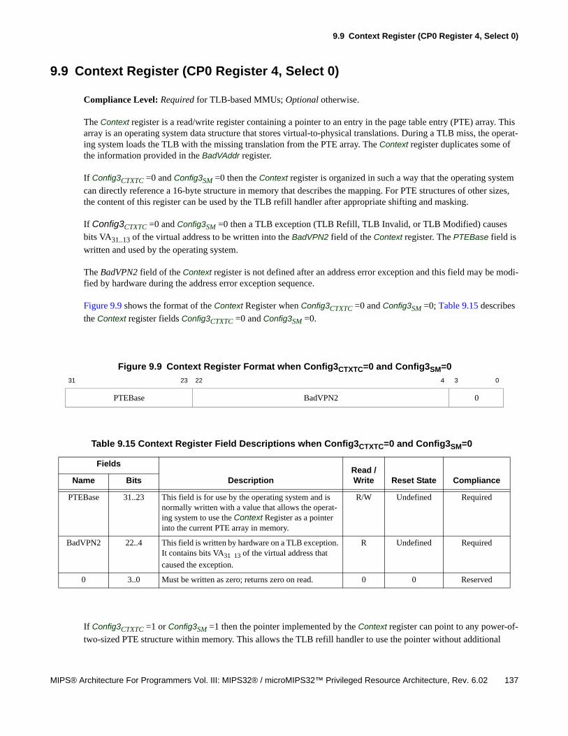
9.9 Context Register (CP0 Register 4, Select 0)
MIPS® Architecture For Programmers Vol. III: MIPS32® / microMIPS32™ Privileged Resource Architecture, Rev. 6.02 137
9.9 Context Register (CP0 Register 4, Select 0)
Compliance Level: Required for TLB-based MMUs; Optional otherwise.
The Context register is a read/write register containing a pointer to an entry in the page table entry (PTE) array. This array is an operating system data structure that stores virtual-to-physical translations. During a TLB miss, the operat-ing system loads the TLB with the missing translation from the PTE array. The Context register duplicates some of the information provided in the BadVAddr register.
If Config3CTXTC =0 and Config3SM =0 then the Context register is organized in such a way that the operating system
can directly reference a 16-byte structure in memory that describes the mapping. For PTE structures of other sizes, the content of this register can be used by the TLB refill handler after appropriate shifting and masking.
If Config3CTXTC =0 and Config3SM =0 then a TLB exception (TLB Refill, TLB Invalid, or TLB Modified) causes
bits VA31..13 of the virtual address to be written into the BadVPN2 field of the Context register. The PTEBase field is
written and used by the operating system.
The BadVPN2 field of the Context register is not defined after an address error exception and this field may be modi-fied by hardware during the address error exception sequence.
Figure 9.9 shows the format of the Context Register when Config3CTXTC =0 and Config3SM =0; Table 9.15 describes
the Context register fields Config3CTXTC =0 and Config3SM =0.
If Config3CTXTC =1 or Config3SM =1 then the pointer implemented by the Context register can point to any power-of-
two-sized PTE structure within memory. This allows the TLB refill handler to use the pointer without additional
Figure 9.9 Context Register Format when Config3CTXTC=0 and Config3SM=0
31 23 22 4 3 0
PTEBase BadVPN2 0
Table 9.15 Context Register Field Descriptions when Config3CTXTC=0 and Config3SM=0
Fields
DescriptionRead / Write Reset State ComplianceName Bits
PTEBase 31..23 This field is for use by the operating system and is normally written with a value that allows the operat-ing system to use the Context Register as a pointer into the current PTE array in memory.
R/W Undefined Required
BadVPN2 22..4 This field is written by hardware on a TLB exception. It contains bits VA31 13 of the virtual address that
caused the exception.
R Undefined Required
0 3..0 Must be written as zero; returns zero on read. 0 0 Reserved
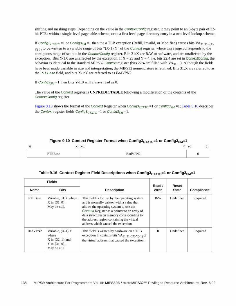
138 MIPS® Architecture For Programmers Vol. III: MIPS32® / microMIPS32™ Privileged Resource Architecture, Rev. 6.02
shifting and masking steps. Depending on the value in the ContextConfig register, it may point to an 8-byte pair of 32-bit PTEs within a single-level page table scheme, or to a first level page directory entry in a two-level lookup scheme.
If Config3CTXTC =1 or Config3SM =1 then the a TLB exception (Refill, Invalid, or Modified) causes bits VA31:31-((X-
Y)-1) to be written to a variable range of bits “(X-1):Y” of the Context register, where this range corresponds to the
contiguous range of set bits in the ContextConfig register. Bits 31:X are R/W to software, and are unaffected by the exception. Bits Y-1:0 are unaffected by the exception. If X = 23 and Y = 4, i.e. bits 22:4 are set in ContextConfig, the behavior is identical to the standard MIPS32 Context register (bits 22:4 are filled with VA31:13). Although the fields
have been made variable in size and interpretation, the MIPS32 nomenclature is retained. Bits 31:X are referred to as the PTEBase field, and bits X-1:Y are referred to as BadVPN2.
If Config3SM =1 then Bits Y-1:0 will always read as 0.
The value of the Context register is UNPREDICTABLE following a modification of the contents of the ContextConfig register.
Figure 9.10 shows the format of the Context Register when Config3CTXTC =1 or Config3SM =1; Table 9.16 describes
the Context register fields Config3CTXTC =1 or Config3SM =1.
Figure 9.10 Context Register Format when Config3CTXTC=1 or Config3SM=1
31 X X-1 Y Y-1 0
PTEBase BadVPN2 0
Table 9.16 Context Register Field Descriptions when Config3CTXTC=1 or Config3SM=1
Fields
DescriptionRead / Write
Reset State ComplianceName Bits
PTEBase Variable, 31:X whereX in {31..0}. May be null.
This field is for use by the operating system and is normally written with a value that allows the operating system to use the Context Register as a pointer to an array of data structures in memory corresponding to the address region containing the virtual address which caused the exception.
R/W Undefined Required
BadVPN2 Variable, (X-1):Y where X in {32..1} and Y in {31..0}.May be null.
This field is written by hardware on a TLB exception. It contains bits VA31:31-((X-Y)-1) of
the virtual address that caused the exception.
R Undefined Required
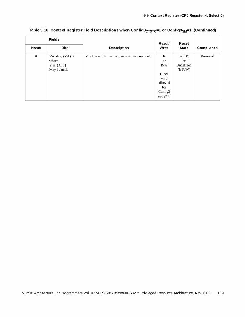
9.9 Context Register (CP0 Register 4, Select 0)
MIPS® Architecture For Programmers Vol. III: MIPS32® / microMIPS32™ Privileged Resource Architecture, Rev. 6.02 139
0 Variable, (Y-1):0where Y in {31:1}.May be null.
Must be written as zero; returns zero on read. Ror
R/W
(R/W only
allowed for
Config3
CTXT=1)
0 (if R)or
Undefined (if R/W)
Reserved
Table 9.16 Context Register Field Descriptions when Config3CTXTC=1 or Config3SM=1 (Continued)
Fields
DescriptionRead / Write
Reset State ComplianceName Bits

140 MIPS® Architecture For Programmers Vol. III: MIPS32® / microMIPS32™ Privileged Resource Architecture, Rev. 6.02
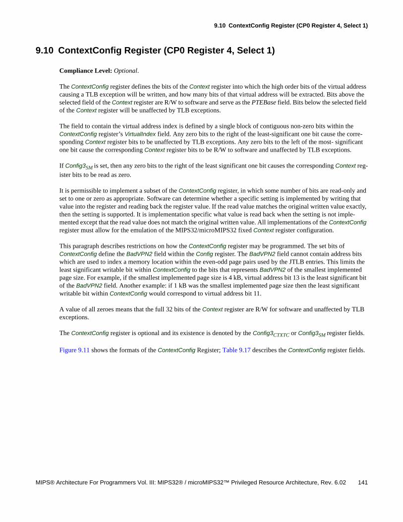
9.10 ContextConfig Register (CP0 Register 4, Select 1)
MIPS® Architecture For Programmers Vol. III: MIPS32® / microMIPS32™ Privileged Resource Architecture, Rev. 6.02 141
9.10 ContextConfig Register (CP0 Register 4, Select 1)
Compliance Level: Optional.
The ContextConfig register defines the bits of the Context register into which the high order bits of the virtual address causing a TLB exception will be written, and how many bits of that virtual address will be extracted. Bits above the selected field of the Context register are R/W to software and serve as the PTEBase field. Bits below the selected field of the Context register will be unaffected by TLB exceptions.
The field to contain the virtual address index is defined by a single block of contiguous non-zero bits within the ContextConfig register’s VirtualIndex field. Any zero bits to the right of the least-significant one bit cause the corre-sponding Context register bits to be unaffected by TLB exceptions. Any zero bits to the left of the most- significant one bit cause the corresponding Context register bits to be R/W to software and unaffected by TLB exceptions.
If Config3SM is set, then any zero bits to the right of the least significant one bit causes the corresponding Context reg-
ister bits to be read as zero.
It is permissible to implement a subset of the ContextConfig register, in which some number of bits are read-only and set to one or zero as appropriate. Software can determine whether a specific setting is implemented by writing that value into the register and reading back the register value. If the read value matches the original written value exactly, then the setting is supported. It is implementation specific what value is read back when the setting is not imple-mented except that the read value does not match the original written value. All implementations of the ContextConfig register must allow for the emulation of the MIPS32/microMIPS32 fixed Context register configuration.
This paragraph describes restrictions on how the ContextConfig register may be programmed. The set bits of ContextConfig define the BadVPN2 field within the Config register. The BadVPN2 field cannot contain address bits which are used to index a memory location within the even-odd page pairs used by the JTLB entries. This limits the least significant writable bit within ContextConfig to the bits that represents BadVPN2 of the smallest implemented page size. For example, if the smallest implemented page size is 4 kB, virtual address bit 13 is the least significant bit of the BadVPN2 field. Another example: if 1 kB was the smallest implemented page size then the least significant writable bit within ContextConfig would correspond to virtual address bit 11.
A value of all zeroes means that the full 32 bits of the Context register are R/W for software and unaffected by TLB exceptions.
The ContextConfig register is optional and its existence is denoted by the Config3CTXTC or Config3SM register fields.
Figure 9.11 shows the formats of the ContextConfig Register; Table 9.17 describes the ContextConfig register fields.
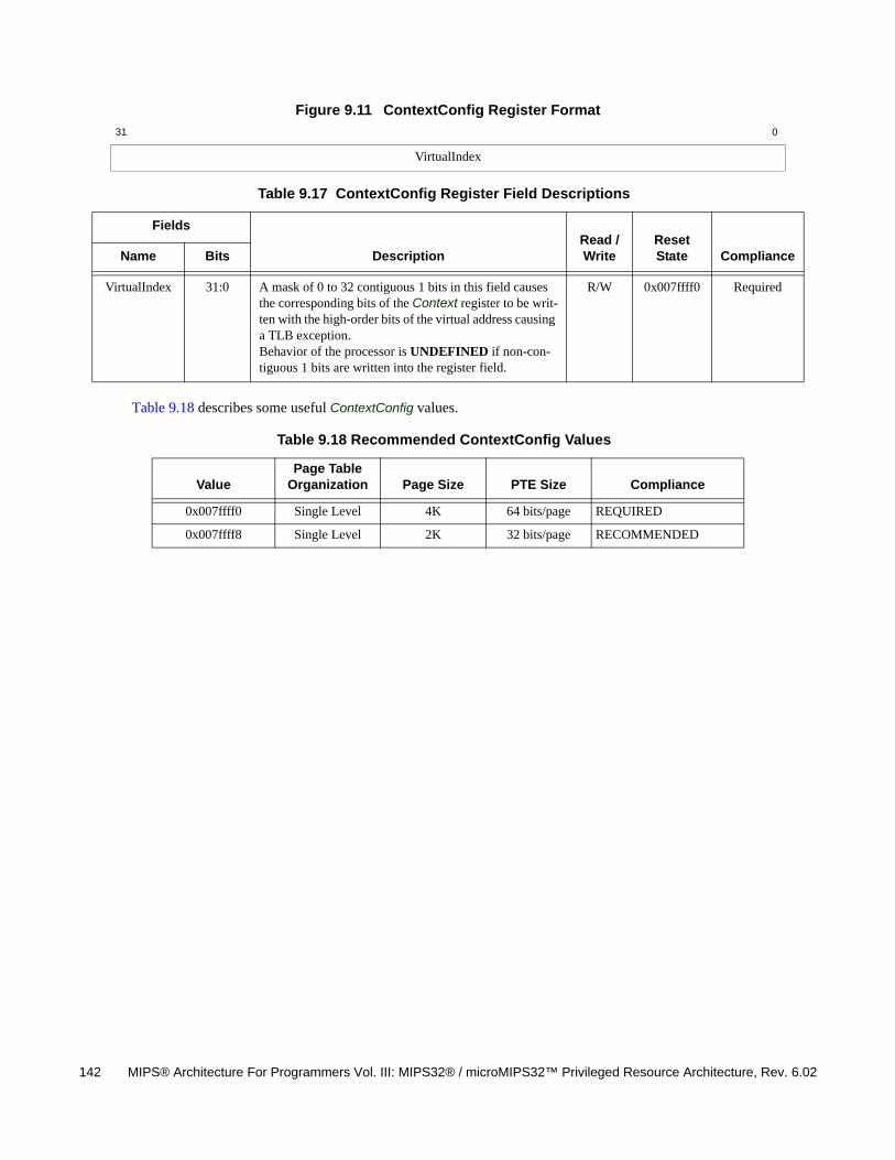
142 MIPS® Architecture For Programmers Vol. III: MIPS32® / microMIPS32™ Privileged Resource Architecture, Rev. 6.02
Figure 9.11 ContextConfig Register Format
Table 9.18 describes some useful ContextConfig values.
31 0
VirtualIndex
Table 9.17 ContextConfig Register Field Descriptions
Fields
DescriptionRead / Write
Reset State ComplianceName Bits
VirtualIndex 31:0 A mask of 0 to 32 contiguous 1 bits in this field causes the corresponding bits of the Context register to be writ-ten with the high-order bits of the virtual address causing a TLB exception.Behavior of the processor is UNDEFINED if non-con-tiguous 1 bits are written into the register field.
R/W 0x007ffff0 Required
Table 9.18 Recommended ContextConfig Values
ValuePage Table
Organization Page Size PTE Size Compliance
0x007ffff0 Single Level 4K 64 bits/page REQUIRED
0x007ffff8 Single Level 2K 32 bits/page RECOMMENDED

9.11 UserLocal Register (CP0 Register 4, Select 2)
MIPS® Architecture For Programmers Vol. III: MIPS32® / microMIPS32™ Privileged Resource Architecture, Rev. 6.02 143
9.11 UserLocal Register (CP0 Register 4, Select 2)
Compliance Level: Pre-Release 6: Recommended.Release 6: Required
The UserLocal register is a read-write register that is not interpreted by the hardware and conditionally readable via the RDHWR instruction.
If the MIPS® MT Module is implemented, the UserLocal register is instantiated per TC.
Prior to Release 6, this register only exists if the Config3ULRI register field is set.
For Release 6, this register is mandatory, and Config3ULRI must be 1.
Figure 9.12 shows the format of the UserLocal register; Table 9.19 describes the UserLocal register fields.
Programming Notes
Privileged software may write this register with arbitrary information and make it accessible to unprivileged softwarevia register 29 (ULR) of the RDHWR instruction. To do so, bit 29 of the HWREna register must be set to a 1 to enableunprivileged access to the register. In some operating environments, the UserLocal register contains a pointer to athread-specific storage block that is obtained via the RDHWR register.
Figure 9.12 UserLocal Register Format
31 0
UserInformation
Table 9.19 UserLocal Register Field Descriptions
Fields
DescriptionRead/Write Reset State ComplianceName Bits
UserInfor-mation
31..0 This field contains software information that is not inter-preted by the hardware.
R/W Undefined Required

144 MIPS® Architecture For Programmers Vol. III: MIPS32® / microMIPS32™ Privileged Resource Architecture, Rev. 6.02
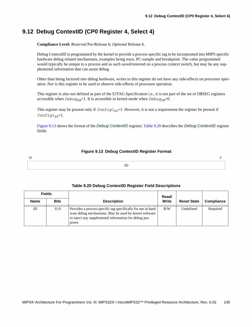
9.12 Debug ContextID (CP0 Register 4, Select 4)
MIPS® Architecture For Programmers Vol. III: MIPS32® / microMIPS32™ Privileged Resource Architecture, Rev. 6.02 145
9.12 Debug ContextID (CP0 Register 4, Select 4)
Compliance Level: Reserved Pre-Release 6; Optional Release 6.
Debug ContextID is programmed by the kernel to provide a process specific tag to be incorporated into MIPS specific hardware debug related mechanisms, examples being trace, PC-sample and breakpoint. The value programmed would typically be unique to a process and as such saved/restored on a process context switch, but may be any sup-plemental information that can assist debug.
Other than being factored into debug hardware, writes to this register do not have any side-effects on processor oper-ation. Nor is this register to be used to observe side-effects of processor operation.
This register is also not defined as part of the EJTAG Specification i.e., it is not part of the set of DRSEG registers accessible when DebugDM=1. It is accessible in kernel-mode when DebugDM=0.
This register may be present only if Config1EP=1. However, it is not a requirement the register be present if
Config1EP=1.
Figure 9.13 shows the format of the Debug ContextID register; Table 9.20 describes the Debug ContextID register fields.
Figure 9.13 Debug ContextID Register Format
31 0
ID
Table 9.20 Debug ContextID Register Field Descriptions
Fields
DescriptionRead/Write Reset State ComplianceName Bits
ID 31:0 Provides a process specific tag specifically for use in hard-ware debug mechanisms. May be used by kernel software to inject any supplemental information for debug pur-poses.
R/W Undefined Required

146 MIPS® Architecture For Programmers Vol. III: MIPS32® / microMIPS32™ Privileged Resource Architecture, Rev. 6.02
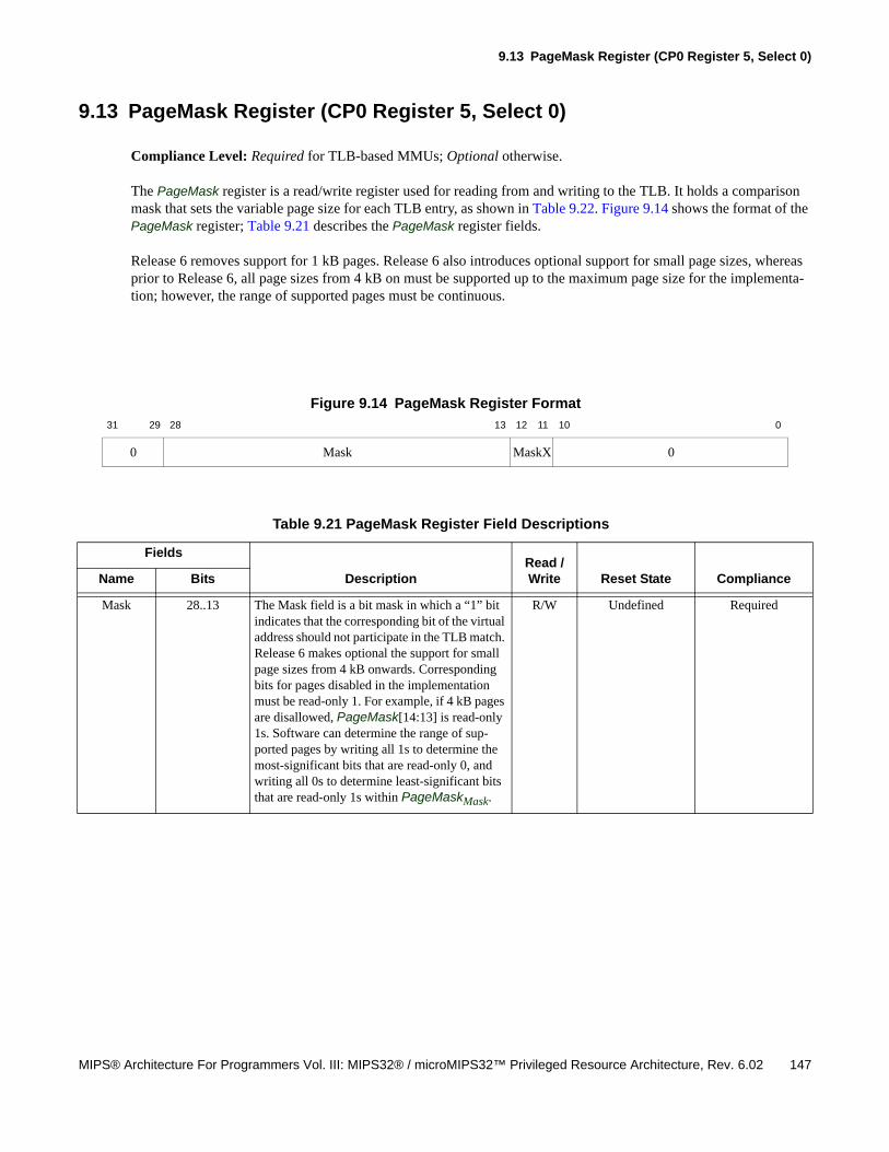
9.13 PageMask Register (CP0 Register 5, Select 0)
MIPS® Architecture For Programmers Vol. III: MIPS32® / microMIPS32™ Privileged Resource Architecture, Rev. 6.02 147
9.13 PageMask Register (CP0 Register 5, Select 0)
Compliance Level: Required for TLB-based MMUs; Optional otherwise.
The PageMask register is a read/write register used for reading from and writing to the TLB. It holds a comparison mask that sets the variable page size for each TLB entry, as shown in Table 9.22. Figure 9.14 shows the format of the PageMask register; Table 9.21 describes the PageMask register fields.
Release 6 removes support for 1 kB pages. Release 6 also introduces optional support for small page sizes, whereas prior to Release 6, all page sizes from 4 kB on must be supported up to the maximum page size for the implementa-tion; however, the range of supported pages must be continuous.
Figure 9.14 PageMask Register Format
31 29 28 13 12 11 10 0
0 Mask MaskX 0
Table 9.21 PageMask Register Field Descriptions
Fields
DescriptionRead / Write Reset State ComplianceName Bits
Mask 28..13 The Mask field is a bit mask in which a “1” bit indicates that the corresponding bit of the virtual address should not participate in the TLB match. Release 6 makes optional the support for small page sizes from 4 kB onwards. Corresponding bits for pages disabled in the implementation must be read-only 1. For example, if 4 kB pages are disallowed, PageMask[14:13] is read-only 1s. Software can determine the range of sup-ported pages by writing all 1s to determine the most-significant bits that are read-only 0, and writing all 0s to determine least-significant bits that are read-only 1s within PageMaskMask.
R/W Undefined Required
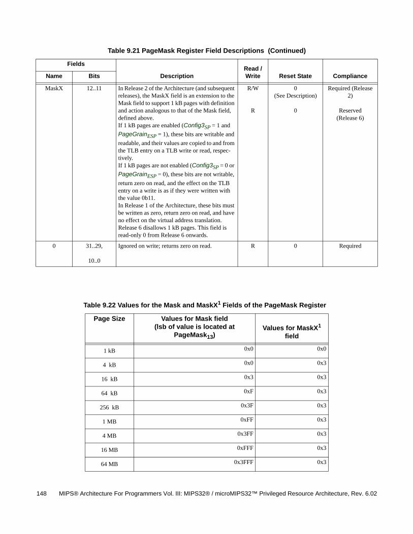
148 MIPS® Architecture For Programmers Vol. III: MIPS32® / microMIPS32™ Privileged Resource Architecture, Rev. 6.02
MaskX 12..11 In Release 2 of the Architecture (and subsequent releases), the MaskX field is an extension to the Mask field to support 1 kB pages with definition and action analogous to that of the Mask field, defined above.If 1 kB pages are enabled (Config3SP = 1 and
PageGrainESP = 1), these bits are writable and
readable, and their values are copied to and from the TLB entry on a TLB write or read, respec-tively.If 1 kB pages are not enabled (Config3SP = 0 or
PageGrainESP = 0), these bits are not writable,
return zero on read, and the effect on the TLB entry on a write is as if they were written with the value 0b11. In Release 1 of the Architecture, these bits must be written as zero, return zero on read, and have no effect on the virtual address translation.Release 6 disallows 1 kB pages. This field is read-only 0 from Release 6 onwards.
R/W
R
0(See Description)
0
Required (Release 2)
Reserved(Release 6)
0 31..29,
10..0
Ignored on write; returns zero on read. R 0 Required
Table 9.22 Values for the Mask and MaskX1 Fields of the PageMask Register
Page Size Values for Mask field (lsb of value is located at
PageMask13)Values for MaskX1
field
1 kB 0x0 0x0
4 kB 0x0 0x3
16 kB 0x3 0x3
64 kB 0xF 0x3
256 kB 0x3F 0x3
1 MB 0xFF 0x3
4 MB 0x3FF 0x3
16 MB 0xFFF 0x3
64 MB 0x3FFF 0x3
Table 9.21 PageMask Register Field Descriptions (Continued)
Fields
DescriptionRead / Write Reset State ComplianceName Bits
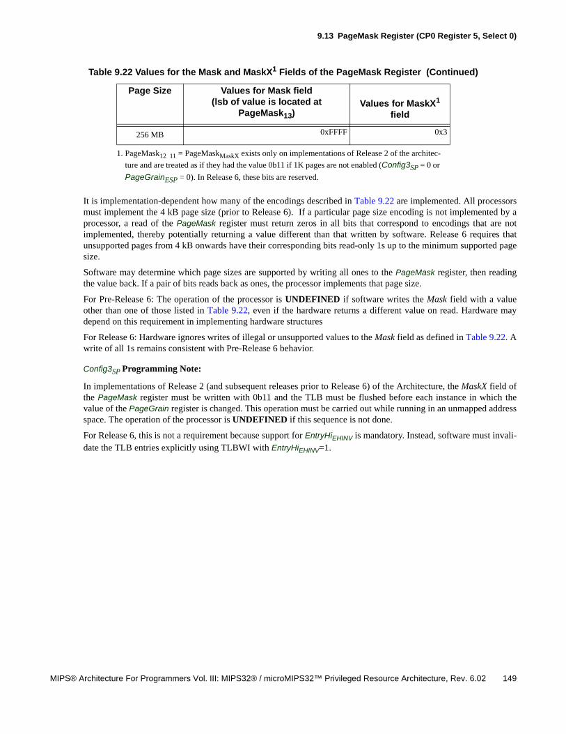
9.13 PageMask Register (CP0 Register 5, Select 0)
MIPS® Architecture For Programmers Vol. III: MIPS32® / microMIPS32™ Privileged Resource Architecture, Rev. 6.02 149
It is implementation-dependent how many of the encodings described in Table 9.22 are implemented. All processorsmust implement the 4 kB page size (prior to Release 6). If a particular page size encoding is not implemented by aprocessor, a read of the PageMask register must return zeros in all bits that correspond to encodings that are notimplemented, thereby potentially returning a value different than that written by software. Release 6 requires thatunsupported pages from 4 kB onwards have their corresponding bits read-only 1s up to the minimum supported pagesize.
Software may determine which page sizes are supported by writing all ones to the PageMask register, then readingthe value back. If a pair of bits reads back as ones, the processor implements that page size.
For Pre-Release 6: The operation of the processor is UNDEFINED if software writes the Mask field with a valueother than one of those listed in Table 9.22, even if the hardware returns a different value on read. Hardware maydepend on this requirement in implementing hardware structures
For Release 6: Hardware ignores writes of illegal or unsupported values to the Mask field as defined in Table 9.22. Awrite of all 1s remains consistent with Pre-Release 6 behavior.
Config3SP Programming Note:
In implementations of Release 2 (and subsequent releases prior to Release 6) of the Architecture, the MaskX field ofthe PageMask register must be written with 0b11 and the TLB must be flushed before each instance in which thevalue of the PageGrain register is changed. This operation must be carried out while running in an unmapped addressspace. The operation of the processor is UNDEFINED if this sequence is not done.
For Release 6, this is not a requirement because support for EntryHiEHINV is mandatory. Instead, software must invali-date the TLB entries explicitly using TLBWI with EntryHiEHINV=1.
256 MB 0xFFFF 0x3
1. PageMask12 11 = PageMaskMaskX exists only on implementations of Release 2 of the architec-
ture and are treated as if they had the value 0b11 if 1K pages are not enabled (Config3SP = 0 or
PageGrainESP = 0). In Release 6, these bits are reserved.
Table 9.22 Values for the Mask and MaskX1 Fields of the PageMask Register (Continued)
Page Size Values for Mask field (lsb of value is located at
PageMask13)Values for MaskX1
field

150 MIPS® Architecture For Programmers Vol. III: MIPS32® / microMIPS32™ Privileged Resource Architecture, Rev. 6.02
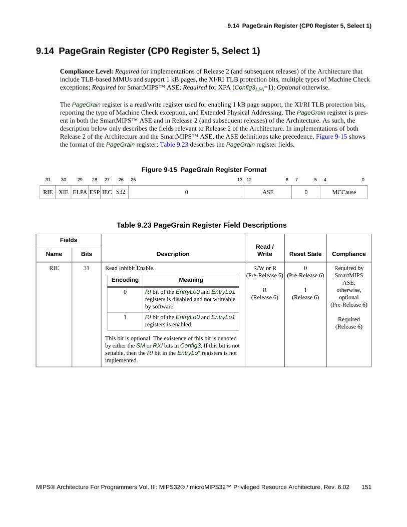
9.14 PageGrain Register (CP0 Register 5, Select 1)
MIPS® Architecture For Programmers Vol. III: MIPS32® / microMIPS32™ Privileged Resource Architecture, Rev. 6.02 151
9.14 PageGrain Register (CP0 Register 5, Select 1)
Compliance Level: Required for implementations of Release 2 (and subsequent releases) of the Architecture that include TLB-based MMUs and support 1 kB pages, the XI/RI TLB protection bits, multiple types of Machine Check exceptions; Required for SmartMIPS™ ASE; Required for XPA (Config3LPA=1); Optional otherwise.
The PageGrain register is a read/write register used for enabling 1 kB page support, the XI/RI TLB protection bits, reporting the type of Machine Check exception, and Extended Physical Addressing. The PageGrain register is pres-ent in both the SmartMIPS™ ASE and in Release 2 (and subsequent releases) of the Architecture. As such, the description below only describes the fields relevant to Release 2 of the Architecture. In implementations of both Release 2 of the Architecture and the SmartMIPS™ ASE, the ASE definitions take precedence. Figure 9-15 shows the format of the PageGrain register; Table 9.23 describes the PageGrain register fields.
Figure 9-15 PageGrain Register Format
31 30 29 28 27 26 25 13 12 8 7 5 4 0
RIE XIE ELPA ESP IEC S32 0 ASE 0 MCCause
Table 9.23 PageGrain Register Field Descriptions
Fields
DescriptionRead / Write Reset State ComplianceName Bits
RIE 31 Read Inhibit Enable.
This bit is optional. The existence of this bit is denoted by either the SM or RXI bits in Config3. If this bit is not settable, then the RI bit in the EntryLo* registers is not implemented.
R/W or R(Pre-Release 6)
R(Release 6)
0(Pre-Release 6)
1(Release 6)
Required by SmartMIPS
ASE;otherwise, optional
(Pre-Release 6)
Required(Release 6)
Encoding Meaning
0 RI bit of the EntryLo0 and EntryLo1 registers is disabled and not writeable by software.
1 RI bit of the EntryLo0 and EntryLo1 registers is enabled.
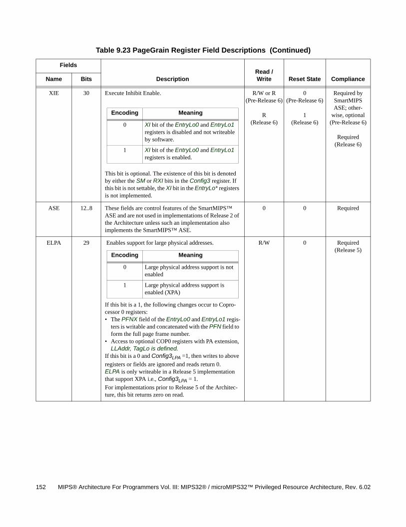
152 MIPS® Architecture For Programmers Vol. III: MIPS32® / microMIPS32™ Privileged Resource Architecture, Rev. 6.02
XIE 30 Execute Inhibit Enable.
This bit is optional. The existence of this bit is denoted by either the SM or RXI bits in the Config3 register. If this bit is not settable, the XI bit in the EntryLo* registers is not implemented.
R/W or R(Pre-Release 6)
R(Release 6)
0(Pre-Release 6)
1(Release 6)
Required by SmartMIPS ASE; other-
wise, optional (Pre-Release 6)
Required(Release 6)
ASE 12..8 These fields are control features of the SmartMIPS™ ASE and are not used in implementations of Release 2 of the Architecture unless such an implementation also implements the SmartMIPS™ ASE.
0 0 Required
ELPA 29 Enables support for large physical addresses.
If this bit is a 1, the following changes occur to Copro-cessor 0 registers:• The PFNX field of the EntryLo0 and EntryLo1 regis-
ters is writable and concatenated with the PFN field to form the full page frame number.
• Access to optional COP0 registers with PA extension, LLAddr, TagLo is defined.
If this bit is a 0 and Config3LPA =1, then writes to above
registers or fields are ignored and reads return 0.ELPA is only writeable in a Release 5 implementation that support XPA i.e., Config3LPA = 1.
For implementations prior to Release 5 of the Architec-ture, this bit returns zero on read.
R/W 0 Required(Release 5)
Table 9.23 PageGrain Register Field Descriptions (Continued)
Fields
DescriptionRead / Write Reset State ComplianceName Bits
Encoding Meaning
0 XI bit of the EntryLo0 and EntryLo1 registers is disabled and not writeable by software.
1 XI bit of the EntryLo0 and EntryLo1 registers is enabled.
Encoding Meaning
0 Large physical address support is not enabled
1 Large physical address support is enabled (XPA)
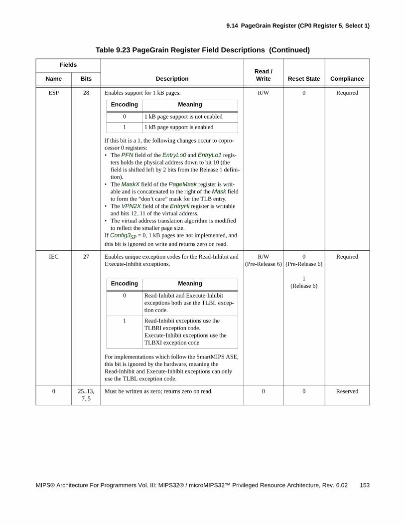
9.14 PageGrain Register (CP0 Register 5, Select 1)
MIPS® Architecture For Programmers Vol. III: MIPS32® / microMIPS32™ Privileged Resource Architecture, Rev. 6.02 153
ESP 28 Enables support for 1 kB pages.
If this bit is a 1, the following changes occur to copro-cessor 0 registers:• The PFN field of the EntryLo0 and EntryLo1 regis-
ters holds the physical address down to bit 10 (the field is shifted left by 2 bits from the Release 1 defini-tion).
• The MaskX field of the PageMask register is writ-able and is concatenated to the right of the Mask field to form the “don’t care” mask for the TLB entry.
• The VPN2X field of the EntryHi register is writable and bits 12..11 of the virtual address.
• The virtual address translation algorithm is modified to reflect the smaller page size.
If Config3SP = 0, 1 kB pages are not implemented, and
this bit is ignored on write and returns zero on read.
R/W 0 Required
IEC 27 Enables unique exception codes for the Read-Inhibit and Execute-Inhibit exceptions.
For implementations which follow the SmartMIPS ASE, this bit is ignored by the hardware, meaning the Read-Inhibit and Execute-Inhibit exceptions can only use the TLBL exception code.
R/W(Pre-Release 6)
0(Pre-Release 6)
1(Release 6)
Required
0 25..13, 7..5
Must be written as zero; returns zero on read. 0 0 Reserved
Table 9.23 PageGrain Register Field Descriptions (Continued)
Fields
DescriptionRead / Write Reset State ComplianceName Bits
Encoding Meaning
0 1 kB page support is not enabled
1 1 kB page support is enabled
Encoding Meaning
0 Read-Inhibit and Execute-Inhibit exceptions both use the TLBL excep-tion code.
1 Read-Inhibit exceptions use the TLBRI exception code. Execute-Inhibit exceptions use the TLBXI exception code
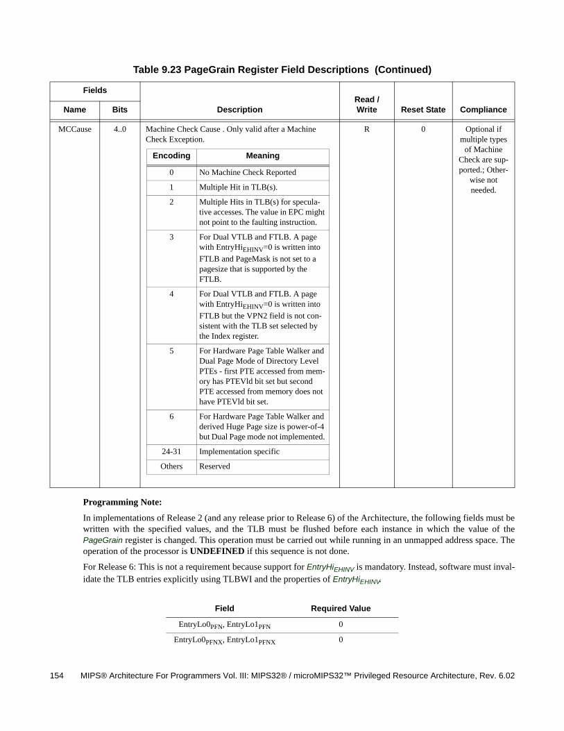
154 MIPS® Architecture For Programmers Vol. III: MIPS32® / microMIPS32™ Privileged Resource Architecture, Rev. 6.02
Programming Note:
In implementations of Release 2 (and any release prior to Release 6) of the Architecture, the following fields must bewritten with the specified values, and the TLB must be flushed before each instance in which the value of thePageGrain register is changed. This operation must be carried out while running in an unmapped address space. Theoperation of the processor is UNDEFINED if this sequence is not done.
For Release 6: This is not a requirement because support for EntryHiEHINV is mandatory. Instead, software must inval-idate the TLB entries explicitly using TLBWI and the properties of EntryHiEHINV.
MCCause 4..0 Machine Check Cause . Only valid after a Machine Check Exception.
R 0 Optional if multiple types
of Machine Check are sup-ported.; Other-
wise not needed.
Field Required Value
EntryLo0PFN, EntryLo1PFN 0
EntryLo0PFNX, EntryLo1PFNX 0
Table 9.23 PageGrain Register Field Descriptions (Continued)
Fields
DescriptionRead / Write Reset State ComplianceName Bits
Encoding Meaning
0 No Machine Check Reported
1 Multiple Hit in TLB(s).
2 Multiple Hits in TLB(s) for specula-tive accesses. The value in EPC might not point to the faulting instruction.
3 For Dual VTLB and FTLB. A page with EntryHiEHINV=0 is written into
FTLB and PageMask is not set to a pagesize that is supported by the FTLB.
4 For Dual VTLB and FTLB. A page with EntryHiEHINV=0 is written into
FTLB but the VPN2 field is not con-sistent with the TLB set selected by the Index register.
5 For Hardware Page Table Walker and Dual Page Mode of Directory Level PTEs - first PTE accessed from mem-ory has PTEVld bit set but second PTE accessed from memory does not have PTEVld bit set.
6 For Hardware Page Table Walker and derived Huge Page size is power-of-4 but Dual Page mode not implemented.
24-31 Implementation specific
Others Reserved
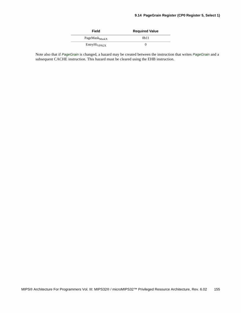
9.14 PageGrain Register (CP0 Register 5, Select 1)
MIPS® Architecture For Programmers Vol. III: MIPS32® / microMIPS32™ Privileged Resource Architecture, Rev. 6.02 155
Note also that if PageGrain is changed, a hazard may be created between the instruction that writes PageGrain and a subsequent CACHE instruction. This hazard must be cleared using the EHB instruction.
PageMaskMaskX 0b11
EntryHiVPN2X 0
Field Required Value

156 MIPS® Architecture For Programmers Vol. III: MIPS32® / microMIPS32™ Privileged Resource Architecture, Rev. 6.02
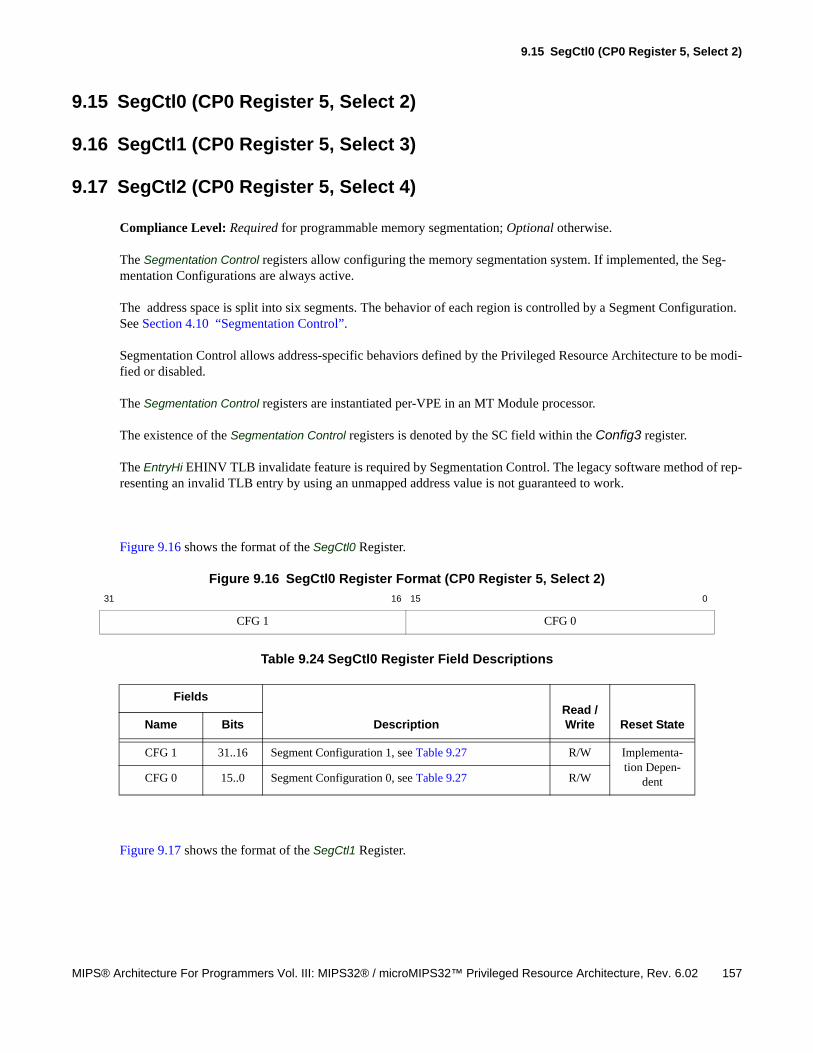
9.15 SegCtl0 (CP0 Register 5, Select 2)
MIPS® Architecture For Programmers Vol. III: MIPS32® / microMIPS32™ Privileged Resource Architecture, Rev. 6.02 157
9.15 SegCtl0 (CP0 Register 5, Select 2)
9.16 SegCtl1 (CP0 Register 5, Select 3)
9.17 SegCtl2 (CP0 Register 5, Select 4)
Compliance Level: Required for programmable memory segmentation; Optional otherwise.
The Segmentation Control registers allow configuring the memory segmentation system. If implemented, the Seg-mentation Configurations are always active.
The address space is split into six segments. The behavior of each region is controlled by a Segment Configuration. See Section 4.10 “Segmentation Control”.
Segmentation Control allows address-specific behaviors defined by the Privileged Resource Architecture to be modi-fied or disabled.
The Segmentation Control registers are instantiated per-VPE in an MT Module processor.
The existence of the Segmentation Control registers is denoted by the SC field within the Config3 register.
The EntryHi EHINV TLB invalidate feature is required by Segmentation Control. The legacy software method of rep-resenting an invalid TLB entry by using an unmapped address value is not guaranteed to work.
Figure 9.16 shows the format of the SegCtl0 Register.
Figure 9.16 SegCtl0 Register Format (CP0 Register 5, Select 2)
Table 9.24 SegCtl0 Register Field Descriptions
Figure 9.17 shows the format of the SegCtl1 Register.
31 16 15 0
CFG 1 CFG 0
Fields
DescriptionRead / Write Reset StateName Bits
CFG 1 31..16 Segment Configuration 1, see Table 9.27 R/W Implementa-tion Depen-
dentCFG 0 15..0 Segment Configuration 0, see Table 9.27 R/W
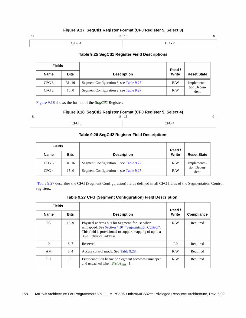
158 MIPS® Architecture For Programmers Vol. III: MIPS32® / microMIPS32™ Privileged Resource Architecture, Rev. 6.02
Figure 9.17 SegCtl1 Register Format (CP0 Register 5, Select 3)
Table 9.25 SegCtl1 Register Field Descriptions
Figure 9.18 shows the format of the SegCtl2 Register.
Figure 9.18 SegCtl2 Register Format (CP0 Register 5, Select 4)
Table 9.26 SegCtl2 Register Field Descriptions
Table 9.27 describes the CFG (Segment Configuration) fields defined in all CFG fields of the Segmentation Control registers.
31 16 15 0
CFG 3 CFG 2
Fields
DescriptionRead / Write Reset StateName Bits
CFG 3 31..16 Segment Configuration 3, see Table 9.27 R/W Implementa-tion Depen-
dentCFG 2 15..0 Segment Configuration 2, see Table 9.27 R/W
31 16 15 0
CFG 5 CFG 4
Fields
DescriptionRead / Write Reset StateName Bits
CFG 5 31..16 Segment Configuration 5, see Table 9.27 R/W Implementa-tion Depen-
dentCFG 4 15..0 Segment Configuration 4, see Table 9.27 R/W
Table 9.27 CFG (Segment Configuration) Field Description
Fields
DescriptionRead / Write ComplianceName Bits
PA 15..9 Physical address bits for Segment, for use when unmapped. See Section 4.10 “Segmentation Control”. This field is provisioned to support mapping of up to a 36-bit physical address.
R/W Required
0 8..7 Reserved. R0 Required
AM 6..4 Access control mode. See Table 9.28. R/W Required
EU 3 Error condition behavior. Segment becomes unmapped and uncached when StatusERL=1.
R/W Required
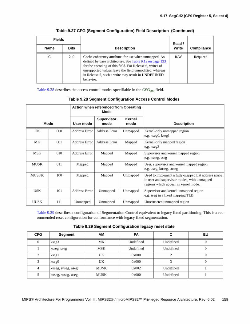
9.17 SegCtl2 (CP0 Register 5, Select 4)
MIPS® Architecture For Programmers Vol. III: MIPS32® / microMIPS32™ Privileged Resource Architecture, Rev. 6.02 159
Table 9.28 describes the access control modes specifiable in the CFGAM field.
Table 9.29 describes a configuration of Segmentation Control equivalent to legacy fixed partitioning. This is a rec-ommended reset configuration for conformance with legacy fixed segmentation.
C 2..0 Cache coherency attribute, for use when unmapped. As defined by base architecture. See Table 9.12 on page 133 for the encoding of this field. For Release 6, writes of unsupported values leave the field unmodified, whereas in Release 5, such a write may result in UNDEFINED behavior.
R/W Required
Table 9.28 Segment Configuration Access Control Modes
Mode
Action when referenced from Operating Mode
DescriptionUser modeSupervisor
modeKernel mode
UK 000 Address Error Address Error Unmapped Kernel-only unmapped regione.g. kseg0, kseg1
MK 001 Address Error Address Error Mapped Kernel-only mapped regione.g. kseg3
MSK 010 Address Error Mapped Mapped Supervisor and kernel mapped regione.g. ksseg, sseg
MUSK 011 Mapped Mapped Mapped User, supervisor and kernel mapped regione.g. useg, kuseg, suseg
MUSUK 100 Mapped Mapped Unmapped Used to implement a fully-mapped flat address space in user and supervisor modes, with unmapped regions which appear in kernel mode.
USK 101 Address Error Unmapped Unmapped Supervisor and kernel unmapped regione.g. sseg in a fixed mapping TLB.
UUSK 111 Unmapped Unmapped Unmapped Unrestricted unmapped region
Table 9.29 Segment Configuration legacy reset state
CFG Segment AM PA C EU
0 kseg3 MK Undefined Undefined 0
1 ksseg, sseg MSK Undefined Undefined 0
2 kseg1 UK 0x000 2 0
3 kseg0 UK 0x000 3 0
4 kuseg, suseg, useg MUSK 0x002 Undefined 1
5 kuseg, suseg, useg MUSK 0x000 Undefined 1
Table 9.27 CFG (Segment Configuration) Field Description (Continued)
Fields
DescriptionRead / Write ComplianceName Bits
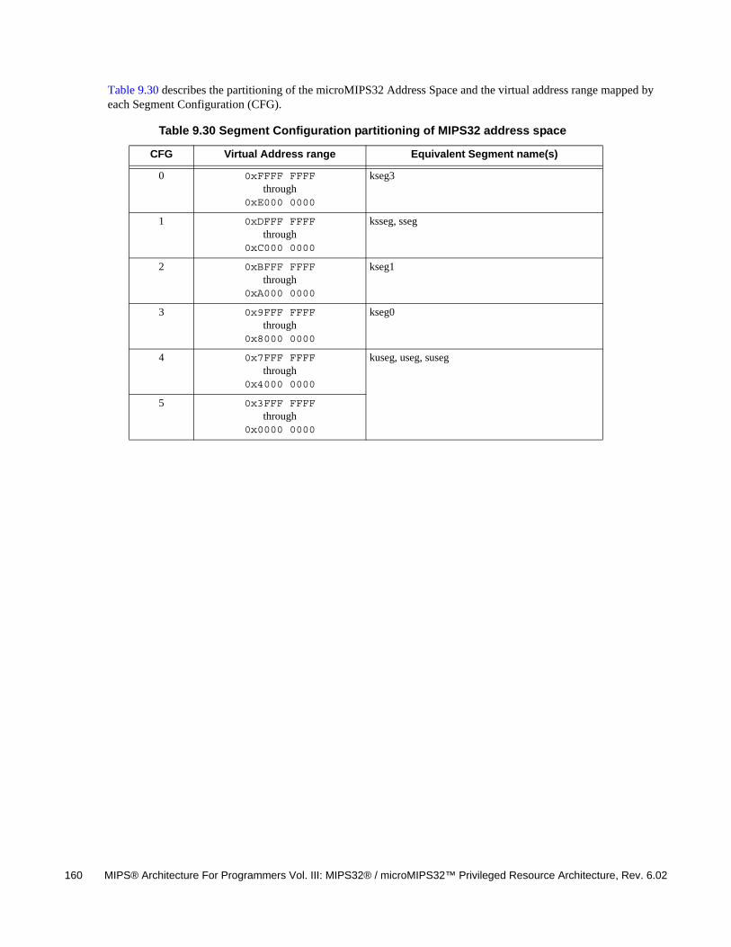
160 MIPS® Architecture For Programmers Vol. III: MIPS32® / microMIPS32™ Privileged Resource Architecture, Rev. 6.02
Table 9.30 describes the partitioning of the microMIPS32 Address Space and the virtual address range mapped by each Segment Configuration (CFG).
Table 9.30 Segment Configuration partitioning of MIPS32 address space
CFG Virtual Address range Equivalent Segment name(s)
0 0xFFFF FFFF through
0xE000 0000
kseg3
1 0xDFFF FFFF through
0xC000 0000
ksseg, sseg
2 0xBFFF FFFF through
0xA000 0000
kseg1
3 0x9FFF FFFF through
0x8000 0000
kseg0
4 0x7FFF FFFF through
0x4000 0000
kuseg, useg, suseg
5 0x3FFF FFFF through
0x0000 0000
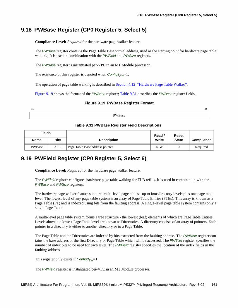
9.18 PWBase Register (CP0 Register 5, Select 5)
MIPS® Architecture For Programmers Vol. III: MIPS32® / microMIPS32™ Privileged Resource Architecture, Rev. 6.02 161
9.18 PWBase Register (CP0 Register 5, Select 5)
Compliance Level: Required for the hardware page walker feature.
The PWBase register contains the Page Table Base virtual address, used as the starting point for hardware page table walking. It is used in combination with the PWField and PWSize registers.
The PWBase register is instantiated per-VPE in an MT Module processor.
The existence of this register is denoted when Config3PW=1.
The operation of page table walking is described in Section 4.12 “Hardware Page Table Walker”.
Figure 9.19 shows the format of the PWBase register; Table 9.31 describes the PWBase register fields.
Figure 9.19 PWBase Register Format
9.19 PWField Register (CP0 Register 5, Select 6)
Compliance Level: Required for the hardware page walker feature.
The PWField register configures hardware page table walking for TLB refills. It is used in combination with the PWBase and PWSize registers.
The hardware page walker feature supports multi-level page tables - up to four directory levels plus one page table level. The lowest level of any page table system is an array of Page Table Entries (PTEs). This array is known as a Page Table (PT) and is indexed using bits from the faulting address. A single-level page table system contains only a single Page Table.
A multi-level page table system forms a tree structure - the lowest (leaf) elements of which are Page Table Entries. Levels above the lowest Page Table level are known as Directories. A directory consists of an array of pointers. Each pointer in a directory is either to another directory or to a Page Table.
The Page Table and the Directories are indexed by bits extracted from the faulting address. The PWBase register con-tains the base address of the first Directory or Page Table which will be accessed. The PWSize register specifies the number of index bits to be used for each level. The PWField register specifies the location of the index fields in the faulting address.
This register only exists if Config3PW=1.
The PWField register is instantiated per-VPE in an MT Module processor.
31 0
PWBase
Table 9.31 PWBase Register Field Descriptions
Fields
DescriptionRead / Write
Reset State ComplianceName Bits
PWBase 31..0 Page Table Base address pointer R/W 0 Required
162 MIPS® Architecture For Programmers Vol. III: MIPS32® / microMIPS32™ Privileged Resource Architecture, Rev. 6.02
If a synchronous exception condition is detected on a read operation during hardware page-table walking, the auto-mated process is aborted and a TLB Refill exception is taken.
Figure 9.20 shows the formats of the PWField Register; Table 9.32 describes the PWField register fields.
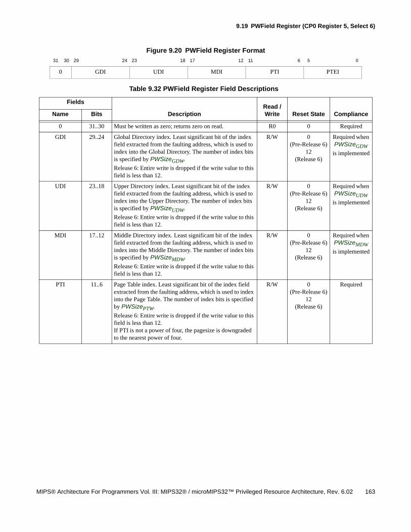
9.19 PWField Register (CP0 Register 5, Select 6)
MIPS® Architecture For Programmers Vol. III: MIPS32® / microMIPS32™ Privileged Resource Architecture, Rev. 6.02 163
Figure 9.20 PWField Register Format
31 30 29 24 23 18 17 12 11 6 5 0
0 GDI UDI MDI PTI PTEI
Table 9.32 PWField Register Field Descriptions
Fields
DescriptionRead / Write Reset State ComplianceName Bits
0 31..30 Must be written as zero; returns zero on read. R0 0 Required
GDI 29..24 Global Directory index. Least significant bit of the index field extracted from the faulting address, which is used to index into the Global Directory. The number of index bits is specified by PWSizeGDW.
Release 6: Entire write is dropped if the write value to this field is less than 12.
R/W 0(Pre-Release 6)
12(Release 6)
Required when PWSizeGDW
is implemented
UDI 23..18 Upper Directory index. Least significant bit of the index field extracted from the faulting address, which is used to index into the Upper Directory. The number of index bits is specified by PWSizeUDW.
Release 6: Entire write is dropped if the write value to this field is less than 12.
R/W 0(Pre-Release 6)
12(Release 6)
Required when PWSizeUDW
is implemented
MDI 17..12 Middle Directory index. Least significant bit of the index field extracted from the faulting address, which is used to index into the Middle Directory. The number of index bits is specified by PWSizeMDW.
Release 6: Entire write is dropped if the write value to this field is less than 12.
R/W 0(Pre-Release 6)
12(Release 6)
Required when PWSizeMDW
is implemented
PTI 11..6 Page Table index. Least significant bit of the index field extracted from the faulting address, which is used to index into the Page Table. The number of index bits is specified by PWSizePTW.
Release 6: Entire write is dropped if the write value to this field is less than 12.If PTI is not a power of four, the pagesize is downgraded to the nearest power of four.
R/W 0(Pre-Release 6)
12(Release 6)
Required
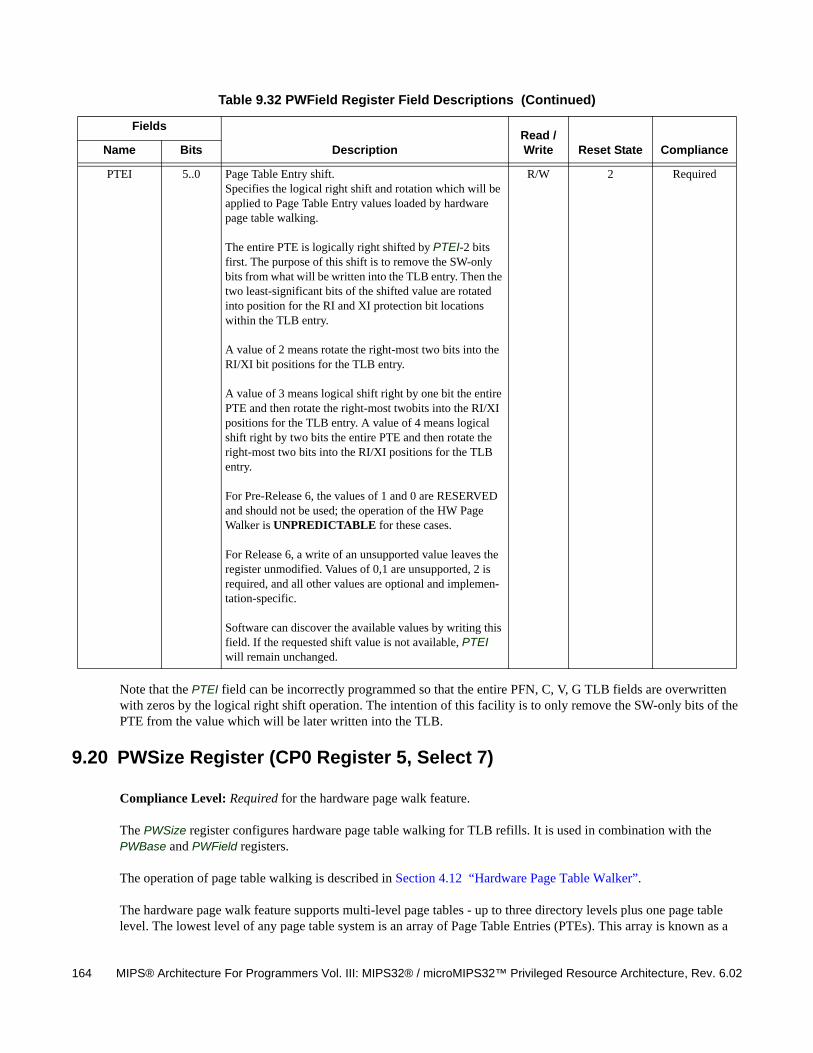
164 MIPS® Architecture For Programmers Vol. III: MIPS32® / microMIPS32™ Privileged Resource Architecture, Rev. 6.02
Note that the PTEI field can be incorrectly programmed so that the entire PFN, C, V, G TLB fields are overwritten with zeros by the logical right shift operation. The intention of this facility is to only remove the SW-only bits of the PTE from the value which will be later written into the TLB.
9.20 PWSize Register (CP0 Register 5, Select 7)
Compliance Level: Required for the hardware page walk feature.
The PWSize register configures hardware page table walking for TLB refills. It is used in combination with the PWBase and PWField registers.
The operation of page table walking is described in Section 4.12 “Hardware Page Table Walker”.
The hardware page walk feature supports multi-level page tables - up to three directory levels plus one page table level. The lowest level of any page table system is an array of Page Table Entries (PTEs). This array is known as a
PTEI 5..0 Page Table Entry shift. Specifies the logical right shift and rotation which will be applied to Page Table Entry values loaded by hardware page table walking.
The entire PTE is logically right shifted by PTEI-2 bits first. The purpose of this shift is to remove the SW-only bits from what will be written into the TLB entry. Then the two least-significant bits of the shifted value are rotated into position for the RI and XI protection bit locations within the TLB entry.
A value of 2 means rotate the right-most two bits into the RI/XI bit positions for the TLB entry.
A value of 3 means logical shift right by one bit the entire PTE and then rotate the right-most twobits into the RI/XI positions for the TLB entry. A value of 4 means logical shift right by two bits the entire PTE and then rotate the right-most two bits into the RI/XI positions for the TLB entry.
For Pre-Release 6, the values of 1 and 0 are RESERVED and should not be used; the operation of the HW Page Walker is UNPREDICTABLE for these cases.
For Release 6, a write of an unsupported value leaves the register unmodified. Values of 0,1 are unsupported, 2 is required, and all other values are optional and implemen-tation-specific.
Software can discover the available values by writing this field. If the requested shift value is not available, PTEI will remain unchanged.
R/W 2 Required
Table 9.32 PWField Register Field Descriptions (Continued)
Fields
DescriptionRead / Write Reset State ComplianceName Bits
9.20 PWSize Register (CP0 Register 5, Select 7)
MIPS® Architecture For Programmers Vol. III: MIPS32® / microMIPS32™ Privileged Resource Architecture, Rev. 6.02 165
Page Table (PT) and is indexed using bits from the faulting address. A single-level page table system contains only a single Page Table.
A multi-level page table system forms a tree structure - the lowest (leaf) elements of which are Page Table Entries. Levels above the lowest Page Table level are known as Directories. A directory consists of an array of pointers. Each pointer in a directory is either to another directory or to a Page Table.
The Page Table and the Directories are indexed by bits extracted from the faulting address BadVAddr. The PWBase register contains the base address of the first Directory or Page Table which will be accessed. The PWSize register specifies the number of index bits to be used for each level. The PWField register specifies the location of the index fields in BadVAddr.
Index values used to access Directories are multiplied by the native pointer size for the refill. For 32-bit addressing, the native pointer size is 32 bits (2 bit left shift). The index value used to access the Page Table is multiplied by the native pointer size. An additional multiplier (left shift value) can be specified using the PWSizePTEW field. This allows space to be allocated in the Page Table structure for software-managed fields.
This register only exists if Config3PW=1.
The PWSize register is instantiated per-VPE in an MT Module processor.
Figure 9.21 shows the formats of the PWSize Register; Table 9.33 describes the PWSize register fields.
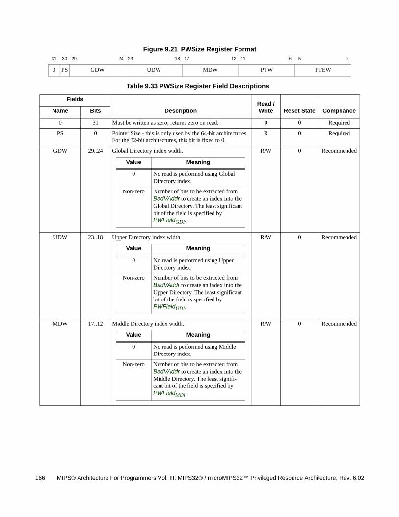
166 MIPS® Architecture For Programmers Vol. III: MIPS32® / microMIPS32™ Privileged Resource Architecture, Rev. 6.02
Figure 9.21 PWSize Register Format
31 30 29 24 23 18 17 12 11 6 5 0
0 PS GDW UDW MDW PTW PTEW
Table 9.33 PWSize Register Field Descriptions
Fields
DescriptionRead / Write Reset State ComplianceName Bits
0 31 Must be written as zero; returns zero on read. 0 0 Required
PS 0 Pointer Size - this is only used by the 64-bit architectures. For the 32-bit architectures, this bit is fixed to 0.
R 0 Required
GDW 29..24 Global Directory index width. R/W 0 Recommended
UDW 23..18 Upper Directory index width. R/W 0 Recommended
MDW 17..12 Middle Directory index width. R/W 0 Recommended
Value Meaning
0 No read is performed using Global Directory index.
Non-zero Number of bits to be extracted from BadVAddr to create an index into the Global Directory. The least significant bit of the field is specified by PWFieldGDI.
Value Meaning
0 No read is performed using Upper Directory index.
Non-zero Number of bits to be extracted from BadVAddr to create an index into the Upper Directory. The least significant bit of the field is specified by PWFieldUDI.
Value Meaning
0 No read is performed using Middle Directory index.
Non-zero Number of bits to be extracted from BadVAddr to create an index into the Middle Directory. The least signifi-cant bit of the field is specified by PWFieldMDI.
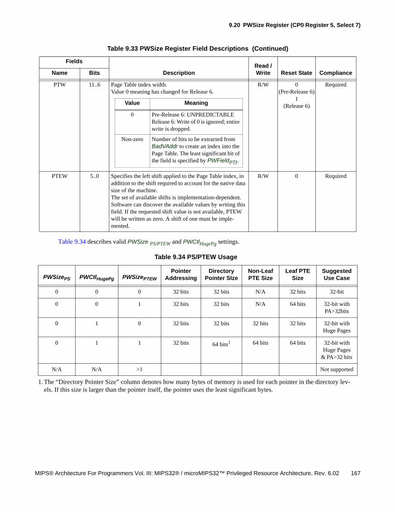
9.20 PWSize Register (CP0 Register 5, Select 7)
MIPS® Architecture For Programmers Vol. III: MIPS32® / microMIPS32™ Privileged Resource Architecture, Rev. 6.02 167
Table 9.34 describes valid PWSize PS/PTEW and PWCtlHugePg settings.
PTW 11..6 Page Table index width.Value 0 meaning has changed for Release 6.
R/W 0(Pre-Release 6)
1(Release 6)
Required
PTEW 5..0 Specifies the left shift applied to the Page Table index, in addition to the shift required to account for the native data size of the machine.The set of available shifts is implementation-dependent. Software can discover the available values by writing this field. If the requested shift value is not available, PTEW will be written as zero. A shift of one must be imple-mented.
R/W 0 Required
Table 9.34 PS/PTEW Usage
PWSizePS PWCtlHugePg PWSizePTEW
Pointer Addressing
Directory Pointer SIze
Non-Leaf PTE Size
Leaf PTE Size
Suggested Use Case
0 0 0 32 bits 32 bits N/A 32 bits 32-bit
0 0 1 32 bits 32 bits N/A 64 bits 32-bit with PA>32bits
0 1 0 32 bits 32 bits 32 bits 32 bits 32-bit with Huge Pages
0 1 1 32 bits 64 bits1
1. The “Directory Pointer Size” column denotes how many bytes of memory is used for each pointer in the directory lev-els. If this size is larger than the pointer itself, the pointer uses the least significant bytes.
64 bits 64 bits 32-bit with Huge Pages
& PA>32 bits
N/A N/A >1 Not supported
Table 9.33 PWSize Register Field Descriptions (Continued)
Fields
DescriptionRead / Write Reset State ComplianceName Bits
Value Meaning
0 Pre-Release 6: UNPREDICTABLERelease 6: Write of 0 is ignored; entire write is dropped.
Non-zero Number of bits to be extracted from BadVAddr to create an index into the Page Table. The least significant bit of the field is specified by PWFieldPTI.

168 MIPS® Architecture For Programmers Vol. III: MIPS32® / microMIPS32™ Privileged Resource Architecture, Rev. 6.02
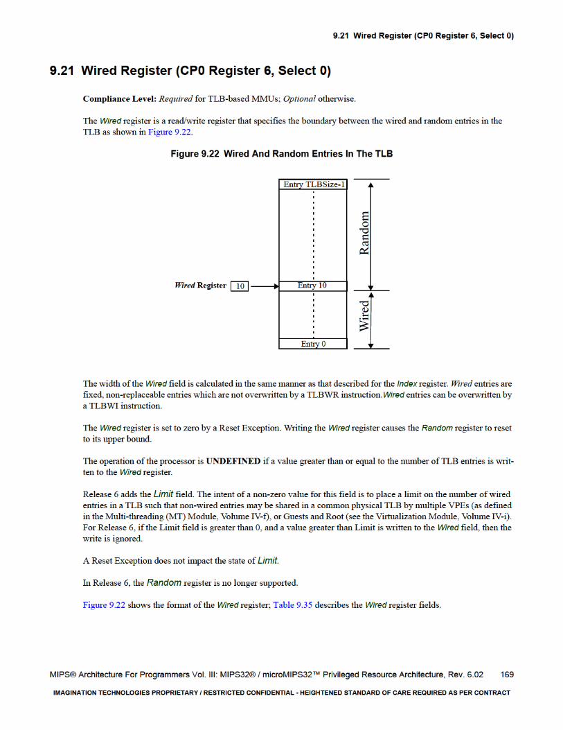
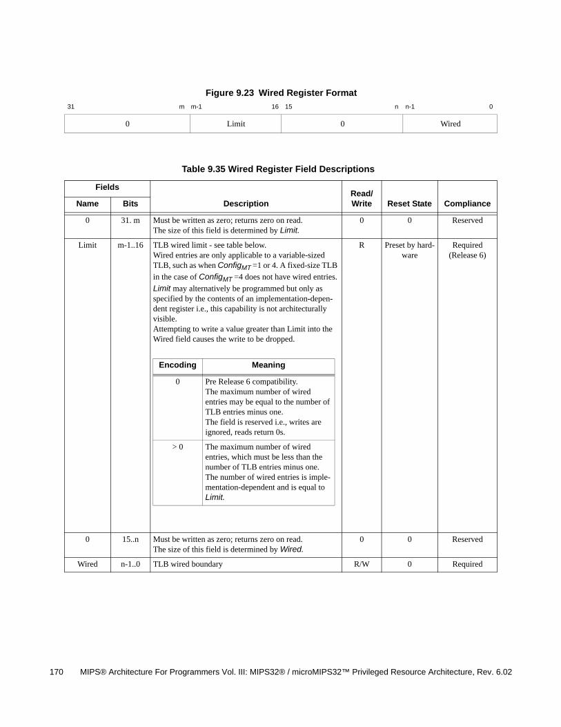
170 MIPS® Architecture For Programmers Vol. III: MIPS32® / microMIPS32™ Privileged Resource Architecture, Rev. 6.02
Figure 9.23 Wired Register Format
31 m m-1 16 15 n n-1 0
0 Limit 0 Wired
Table 9.35 Wired Register Field Descriptions
Fields
DescriptionRead/Write Reset State ComplianceName Bits
0 31. m Must be written as zero; returns zero on read.The size of this field is determined by Limit.
0 0 Reserved
Limit m-1..16 TLB wired limit - see table below.Wired entries are only applicable to a variable-sized TLB, such as when ConfigMT =1 or 4. A fixed-size TLB
in the case of ConfigMT =4 does not have wired entries.
Limit may alternatively be programmed but only as specified by the contents of an implementation-depen-dent register i.e., this capability is not architecturally visible.Attempting to write a value greater than Limit into the Wired field causes the write to be dropped.
R Preset by hard-ware
Required(Release 6)
0 15..n Must be written as zero; returns zero on read.The size of this field is determined by Wired.
0 0 Reserved
Wired n-1..0 TLB wired boundary R/W 0 Required
Encoding Meaning
0 Pre Release 6 compatibility.The maximum number of wired entries may be equal to the number of TLB entries minus one. The field is reserved i.e., writes are ignored, reads return 0s.
> 0 The maximum number of wired entries, which must be less than the number of TLB entries minus one. The number of wired entries is imple-mentation-dependent and is equal to Limit.
9.22 PWCtl Register (CP0 Register 6, Select 6)
MIPS® Architecture For Programmers Vol. III: MIPS32® / microMIPS32™ Privileged Resource Architecture, Rev. 6.02 171
9.22 PWCtl Register (CP0 Register 6, Select 6)
Compliance Level: Required for the hardware page walker feature.
The PWCtl register configures hardware page table walking for TLB refills. It is used in combination with the PWBase, PWField and PWSize registers.
Hardware page table walking is disabled when PWCtlPWEn=0.
The hardware page walker feature supports multi-level page tables - up to four directory levels plus one page table level. The lowest level of any page table system is an array of Page Table Entries (PTEs). This array is known as a Page Table (PT) and is indexed using bits from the faulting address. A single-level page table system contains only a single Page Table.
A multi-level page table system forms a tree structure - the lowest (leaf) elements of which are Page Table Entries. Levels above the lowest Page Table level are known as Directories. A directory consists of an array of pointers. Each pointer in a directory is either to another directory or to a Page Table.
The Page Table and the Directories are indexed by bits extracted from the faulting address BadVAddr. The PWBase register contains the base address of the first Directory or Page Table which will be accessed. The PWSize register specifies the number of index bits to be used for each level. The PWField register specifies the location of the index fields in BadVAddr.
The existence of this register is denoted when Config3PW=1.
The PWField register is instantiated per-VPE in an MT Module processor.
Figure 9.24 shows the formats of the PWCtl Register; Table 9.36 describes the PWCtl register fields.
172 MIPS® Architecture For Programmers Vol. III: MIPS32® / microMIPS32™ Privileged Resource Architecture, Rev. 6.02
Figure 9.24 PWCtl Register Format
If the implementation supports Huge Pages, then Software enables Huge Pages by setting PWCtlHugePg=1. Software
can disable Huge Pages by setting PWCtlHugePg = 0. An implementation that does not support Huge Pages is required
to hardwire PWCtlHugetPg = 0 read-only. Software can determine Huge Page support by writing 1 to PWCtlHugePg, if a
following read returns 0, then Huge Page support is not implemented.
The PWCtlPsn field is provisioned at 6 bits, allowing a starting bit position for PTEvld up to bit 64 in the PTE. An implementation may choose to support a more limited range by hardwiring an implementation defined number of the high order bits of PWCtlPsn to 0. Software can determine the supported range by writing ones to PWCtlPsn then read-
ing.
For non-Leaf
31 30 7 6 5..0
PWEn Reserved DPH HugePg Psn
Table 9.36 PWCtl Register Field Descriptions
Fields
DescriptionRead / Write
Reset State ComplianceName Bits
PWEn 31 Hardware Page Table walker enableIf this bit is set, then the Hardware Page Table is enabled.
R/W 0 Required
- 30..8 Reserved, Must be written as zero; returns zero on read. R0 0 Required
DPH 7 Dual Page format of Huge Page support. This bit is only used when HugePg=1.
If DPH bit is set, then a Huge Page PTE can represent a power-of-4 memory region or a 2x power-of-4 memory region. For the first case, one PTE is used for even TLB page and the adjacent PTE is used for the odd PTE. For the latter case, the Hardware will synthesize the physical addresses for both the even and odd TLB pages from the single PTE entry.
If DPH bit is clear, then a Huge Page PTE can only repre-sent a region that is 2 x power-of-4 in size. For this case, the Hardware will synthesize the physical addresses for both the even and odd TLB pages from the single PTE entry.
R or R/W 0 Required
HugePg 6 Huge Page PTE supported in Directory levels. If this bit is set, then Huge Page PTE in non-leaf table (i.e., directory level) is supported.
R or R/W 0 Required
PSn 5:0 Bit position of PTEvld in Huge Page PTE. Only used when HugePg field is set.
R/W 0 Required
9.22 PWCtl Register (CP0 Register 6, Select 6)
MIPS® Architecture For Programmers Vol. III: MIPS32® / microMIPS32™ Privileged Resource Architecture, Rev. 6.02 173
Table 9.37 describes how the HugePg field is used to denote whether Huge Pages are supported or not.
Table 9.38 describes how Huge Pages are represented in the Directory Levels.
Table 9.37 HugePg Field and Huge Page configurations
PWCTLHugePg
Type of EntryRsvd Field in Non-
leaf entry CommentNon-Leaf Leaf
0 Always Pointer
PTEPTEVld not used
Always PTE
PTEPTEVld not used
X No Huge-Page Support
1 PTEPTEVld=0 means Pointer
PTEPTEVld=1 means Huge Page
Always PTE
PTEPTEVld not used
Must be 0 Huge-Page Support
Table 9.38 Huge Page representation in Directory Levels
PWCTLDPH
Size of Huge Page
CommentPower of 4 non-Power of 4
0 Not Allowed
If encountered, HW Page Walker aborts and TLB Refill exception
is taken.
Allowed
Even TLB page and Odd TLB page entries both derived from single PTE
Huge-Page region can only be 2x power-of-4
1 Allowed
Two PTEs are read from mem-ory by the HW Page Walker to be used for the Even and Odd TLB page entries.
Allowed
Even TLB page and Odd TLB page entries both derived from single PTE
Huge-Page region can be any power-of- 2
(either power of 4 or 2x power-of-4)

174 MIPS® Architecture For Programmers Vol. III: MIPS32® / microMIPS32™ Privileged Resource Architecture, Rev. 6.02
9.23 HWREna Register (CP0 Register 7, Select 0)
MIPS® Architecture For Programmers Vol. III: MIPS32® / microMIPS32™ Privileged Resource Architecture, Rev. 6.02 175
9.23 HWREna Register (CP0 Register 7, Select 0)
Compliance Level: Required (Release 2).
The HWREna register contains a bit mask that determines which hardware registers are accessible via the RDHWR instruction when that instruction is executed in a mode in which coprocessor 0 is not enabled.
Release 6 adds access to CP0 PerfCnt and Config5XNP.
Figure 9.25 shows the format of the HWREna Register; Table 9.39 describes the HWREna register fields.
Figure 9.25 HWREna Register Format
31 30 29 4 3 0
Impl Mask
Table 9.39 HWREna Register Field Descriptions
Fields
DescriptionRead / Write
Reset State ComplianceName Bits
31..30 Impl These bits enable access to the implementation-dependent hardware registers 31 and 30.
If a register is not implemented, the corresponding bit returns a zero and is ignored on write.
If a register is implemented, access to that register is enabled if the corresponding bit in this field is a 1 and disabled if the corresponding bit is a 0.
R/W 0 Optional - Reserved for Implementations
Mask 29..0 Each bit in this field enables access by the RDHWR instruction to a particular hardware register (which may not be an actual register).
If RDHWR register ‘n’ is not implemented, bit ‘n’ of this field returns a zero and is ignored on a write.
If RDHWR register ‘n’ is implemented, access to the register is enabled if bit ‘n’ in this field is a 1 and dis-abled if bit ‘n’ of this field is a 0.See the RDHWR instruction for a list of valid hard-ware registers.
Table 9.40 lists the RDHWR registers, and register number ‘n’ corresponds to bit ‘n’ in this field.
R/W 0 Required
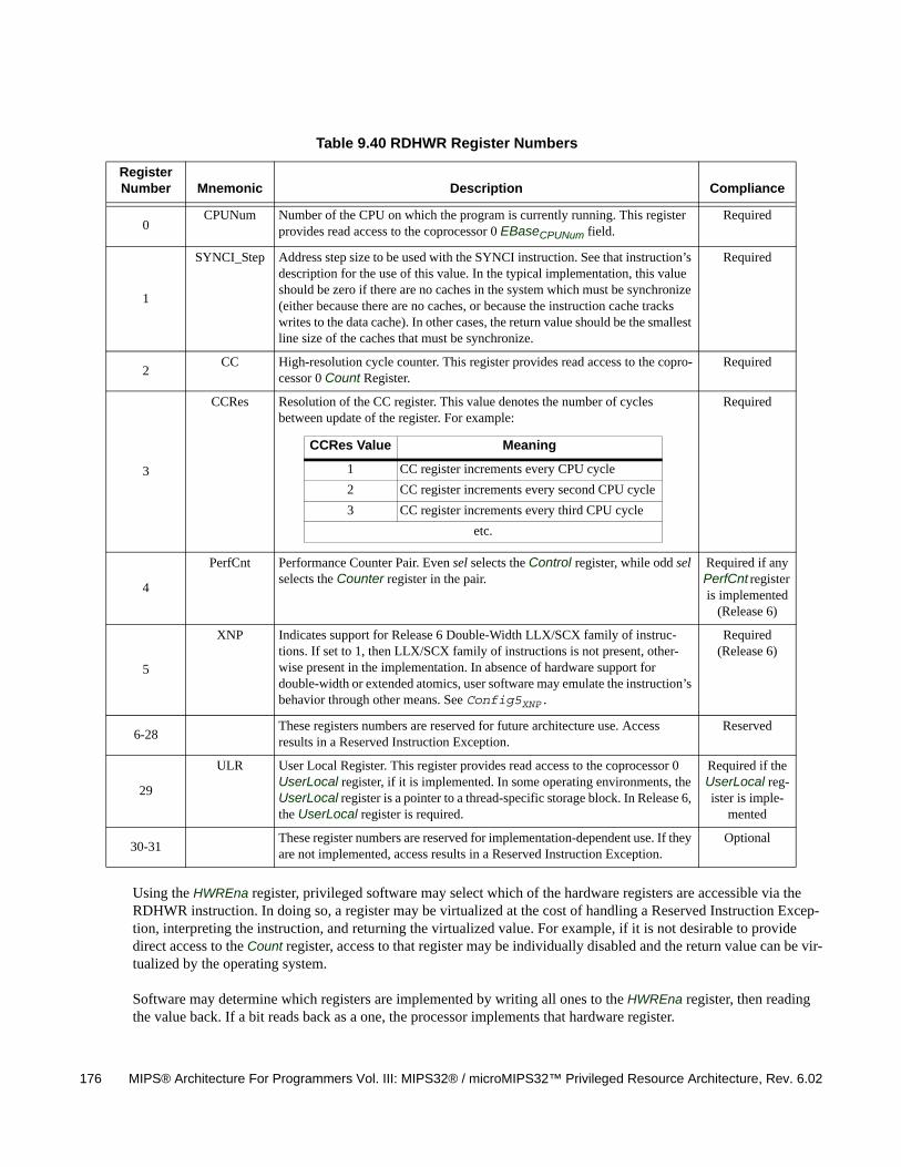
176 MIPS® Architecture For Programmers Vol. III: MIPS32® / microMIPS32™ Privileged Resource Architecture, Rev. 6.02
Using the HWREna register, privileged software may select which of the hardware registers are accessible via the RDHWR instruction. In doing so, a register may be virtualized at the cost of handling a Reserved Instruction Excep-tion, interpreting the instruction, and returning the virtualized value. For example, if it is not desirable to provide direct access to the Count register, access to that register may be individually disabled and the return value can be vir-tualized by the operating system.
Software may determine which registers are implemented by writing all ones to the HWREna register, then reading the value back. If a bit reads back as a one, the processor implements that hardware register.
Table 9.40 RDHWR Register Numbers
Register Number Mnemonic Description Compliance
0CPUNum Number of the CPU on which the program is currently running. This register
provides read access to the coprocessor 0 EBaseCPUNum field.Required
1
SYNCI_Step Address step size to be used with the SYNCI instruction. See that instruction’s description for the use of this value. In the typical implementation, this value should be zero if there are no caches in the system which must be synchronize (either because there are no caches, or because the instruction cache tracks writes to the data cache). In other cases, the return value should be the smallest line size of the caches that must be synchronize.
Required
2CC High-resolution cycle counter. This register provides read access to the copro-
cessor 0 Count Register.Required
3
CCRes Resolution of the CC register. This value denotes the number of cycles between update of the register. For example:
Required
4
PerfCnt Performance Counter Pair. Even sel selects the Control register, while odd sel selects the Counter register in the pair.
Required if any PerfCnt register is implemented
(Release 6)
5
XNP Indicates support for Release 6 Double-Width LLX/SCX family of instruc-tions. If set to 1, then LLX/SCX family of instructions is not present, other-wise present in the implementation. In absence of hardware support for double-width or extended atomics, user software may emulate the instruction’s behavior through other means. See Config5XNP.
Required (Release 6)
6-28These registers numbers are reserved for future architecture use. Access results in a Reserved Instruction Exception.
Reserved
29
ULR User Local Register. This register provides read access to the coprocessor 0 UserLocal register, if it is implemented. In some operating environments, the UserLocal register is a pointer to a thread-specific storage block. In Release 6, the UserLocal register is required.
Required if the UserLocal reg-ister is imple-
mented
30-31These register numbers are reserved for implementation-dependent use. If they are not implemented, access results in a Reserved Instruction Exception.
Optional
CCRes Value Meaning
1 CC register increments every CPU cycle
2 CC register increments every second CPU cycle
3 CC register increments every third CPU cycle
etc.
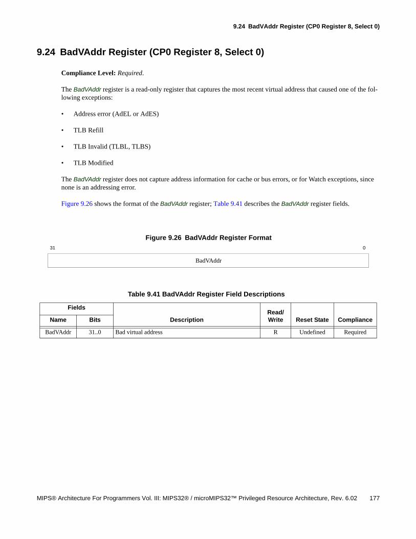
9.24 BadVAddr Register (CP0 Register 8, Select 0)
MIPS® Architecture For Programmers Vol. III: MIPS32® / microMIPS32™ Privileged Resource Architecture, Rev. 6.02 177
9.24 BadVAddr Register (CP0 Register 8, Select 0)
Compliance Level: Required.
The BadVAddr register is a read-only register that captures the most recent virtual address that caused one of the fol-lowing exceptions:
• Address error (AdEL or AdES)
• TLB Refill
• TLB Invalid (TLBL, TLBS)
• TLB Modified
The BadVAddr register does not capture address information for cache or bus errors, or for Watch exceptions, since none is an addressing error.
Figure 9.26 shows the format of the BadVAddr register; Table 9.41 describes the BadVAddr register fields.
Figure 9.26 BadVAddr Register Format
31 0
BadVAddr
Table 9.41 BadVAddr Register Field Descriptions
Fields
DescriptionRead/Write Reset State ComplianceName Bits
BadVAddr 31..0 Bad virtual address R Undefined Required

178 MIPS® Architecture For Programmers Vol. III: MIPS32® / microMIPS32™ Privileged Resource Architecture, Rev. 6.02
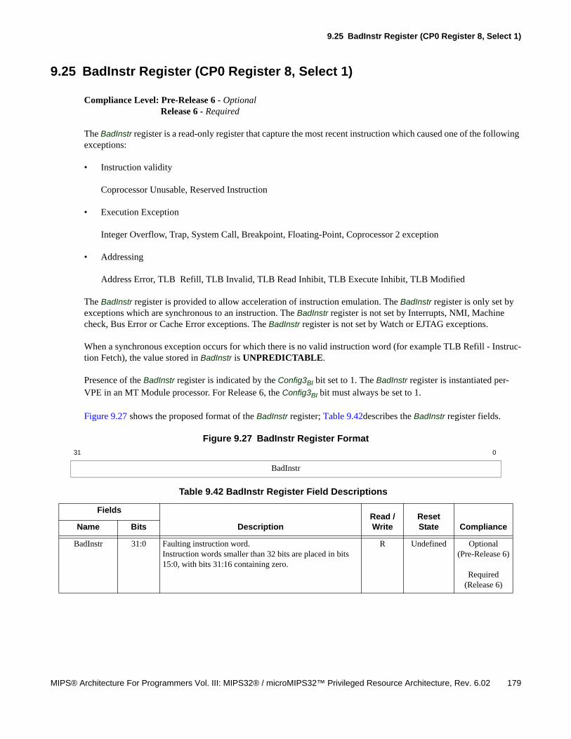
9.25 BadInstr Register (CP0 Register 8, Select 1)
MIPS® Architecture For Programmers Vol. III: MIPS32® / microMIPS32™ Privileged Resource Architecture, Rev. 6.02 179
9.25 BadInstr Register (CP0 Register 8, Select 1)
Compliance Level: Pre-Release 6 - Optional Release 6 - Required
The BadInstr register is a read-only register that capture the most recent instruction which caused one of the following exceptions:
• Instruction validity
Coprocessor Unusable, Reserved Instruction
• Execution Exception
Integer Overflow, Trap, System Call, Breakpoint, Floating-Point, Coprocessor 2 exception
• Addressing
Address Error, TLB Refill, TLB Invalid, TLB Read Inhibit, TLB Execute Inhibit, TLB Modified
The BadInstr register is provided to allow acceleration of instruction emulation. The BadInstr register is only set by exceptions which are synchronous to an instruction. The BadInstr register is not set by Interrupts, NMI, Machine check, Bus Error or Cache Error exceptions. The BadInstr register is not set by Watch or EJTAG exceptions.
When a synchronous exception occurs for which there is no valid instruction word (for example TLB Refill - Instruc-tion Fetch), the value stored in BadInstr is UNPREDICTABLE.
Presence of the BadInstr register is indicated by the Config3BI bit set to 1. The BadInstr register is instantiated per-VPE in an MT Module processor. For Release 6, the Config3BI bit must always be set to 1.
Figure 9.27 shows the proposed format of the BadInstr register; Table 9.42describes the BadInstr register fields.
Figure 9.27 BadInstr Register Format
31 0
BadInstr
Table 9.42 BadInstr Register Field Descriptions
Fields
DescriptionRead / Write
Reset State ComplianceName Bits
BadInstr 31:0 Faulting instruction word. Instruction words smaller than 32 bits are placed in bits 15:0, with bits 31:16 containing zero.
R Undefined Optional(Pre-Release 6)
Required (Release 6)

180 MIPS® Architecture For Programmers Vol. III: MIPS32® / microMIPS32™ Privileged Resource Architecture, Rev. 6.02
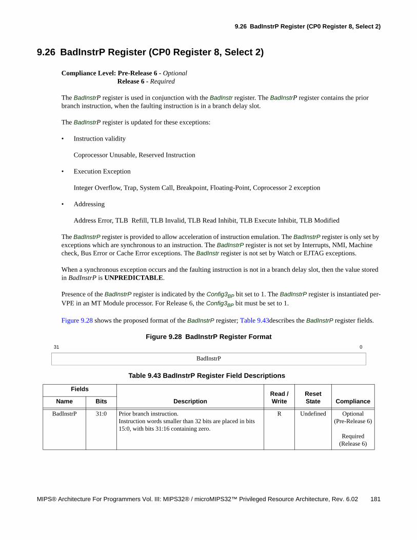
9.26 BadInstrP Register (CP0 Register 8, Select 2)
MIPS® Architecture For Programmers Vol. III: MIPS32® / microMIPS32™ Privileged Resource Architecture, Rev. 6.02 181
9.26 BadInstrP Register (CP0 Register 8, Select 2)
Compliance Level: Pre-Release 6 - OptionalRelease 6 - Required
The BadInstrP register is used in conjunction with the BadInstr register. The BadInstrP register contains the prior branch instruction, when the faulting instruction is in a branch delay slot.
The BadInstrP register is updated for these exceptions:
• Instruction validity
Coprocessor Unusable, Reserved Instruction
• Execution Exception
Integer Overflow, Trap, System Call, Breakpoint, Floating-Point, Coprocessor 2 exception
• Addressing
Address Error, TLB Refill, TLB Invalid, TLB Read Inhibit, TLB Execute Inhibit, TLB Modified
The BadInstrP register is provided to allow acceleration of instruction emulation. The BadInstrP register is only set by exceptions which are synchronous to an instruction. The BadInstrP register is not set by Interrupts, NMI, Machine check, Bus Error or Cache Error exceptions. The BadInstr register is not set by Watch or EJTAG exceptions.
When a synchronous exception occurs and the faulting instruction is not in a branch delay slot, then the value stored in BadInstrP is UNPREDICTABLE.
Presence of the BadInstrP register is indicated by the Config3BP bit set to 1. The BadInstrP register is instantiated per-VPE in an MT Module processor. For Release 6, the Config3BP bit must be set to 1.
Figure 9.28 shows the proposed format of the BadInstrP register; Table 9.43describes the BadInstrP register fields.
Figure 9.28 BadInstrP Register Format
31 0
BadInstrP
Table 9.43 BadInstrP Register Field Descriptions
Fields
DescriptionRead / Write
Reset State ComplianceName Bits
BadInstrP 31:0 Prior branch instruction. Instruction words smaller than 32 bits are placed in bits 15:0, with bits 31:16 containing zero.
R Undefined Optional(Pre-Release 6)
Required (Release 6)

182 MIPS® Architecture For Programmers Vol. III: MIPS32® / microMIPS32™ Privileged Resource Architecture, Rev. 6.02
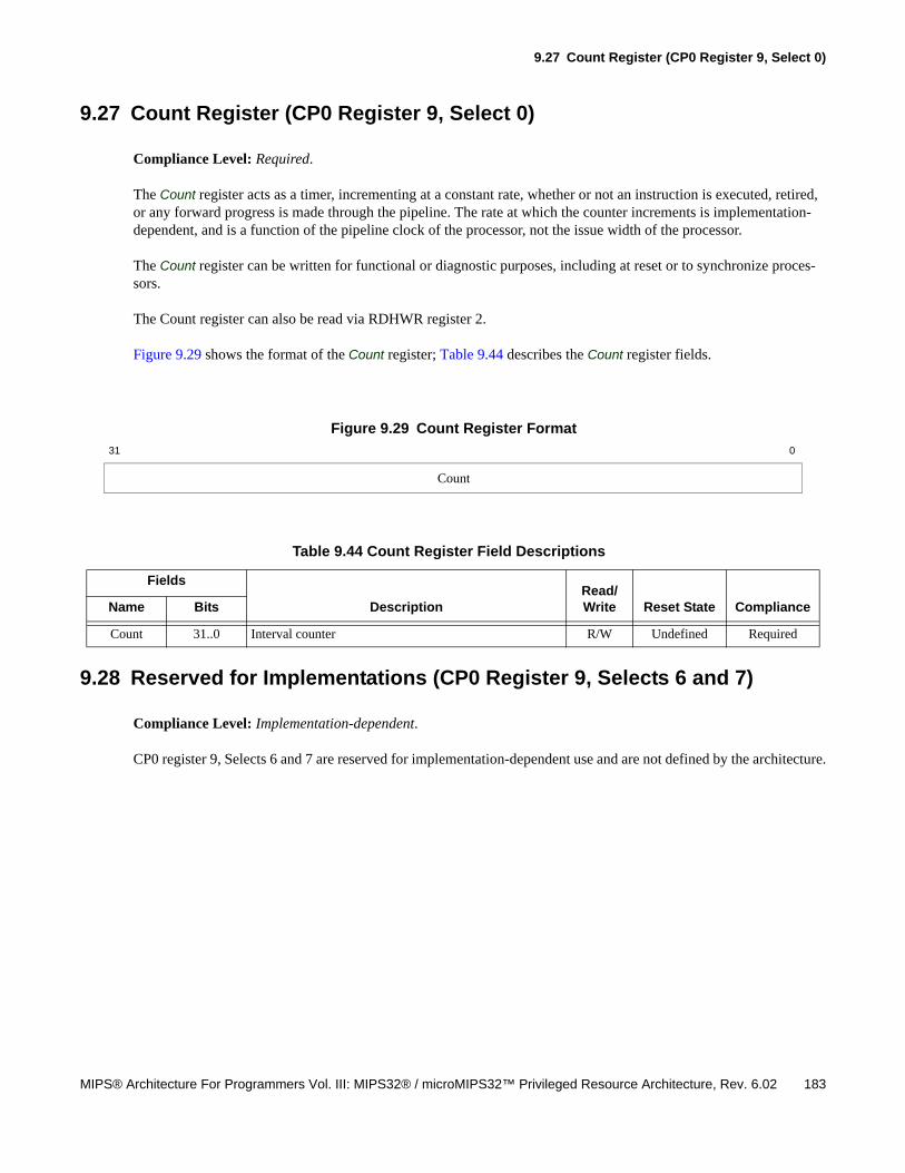
9.27 Count Register (CP0 Register 9, Select 0)
MIPS® Architecture For Programmers Vol. III: MIPS32® / microMIPS32™ Privileged Resource Architecture, Rev. 6.02 183
9.27 Count Register (CP0 Register 9, Select 0)
Compliance Level: Required.
The Count register acts as a timer, incrementing at a constant rate, whether or not an instruction is executed, retired, or any forward progress is made through the pipeline. The rate at which the counter increments is implementation-dependent, and is a function of the pipeline clock of the processor, not the issue width of the processor.
The Count register can be written for functional or diagnostic purposes, including at reset or to synchronize proces-sors.
The Count register can also be read via RDHWR register 2.
Figure 9.29 shows the format of the Count register; Table 9.44 describes the Count register fields.
9.28 Reserved for Implementations (CP0 Register 9, Selects 6 and 7)
Compliance Level: Implementation-dependent.
CP0 register 9, Selects 6 and 7 are reserved for implementation-dependent use and are not defined by the architecture.
Figure 9.29 Count Register Format
31 0
Count
Table 9.44 Count Register Field Descriptions
Fields
DescriptionRead/Write Reset State ComplianceName Bits
Count 31..0 Interval counter R/W Undefined Required

184 MIPS® Architecture For Programmers Vol. III: MIPS32® / microMIPS32™ Privileged Resource Architecture, Rev. 6.02
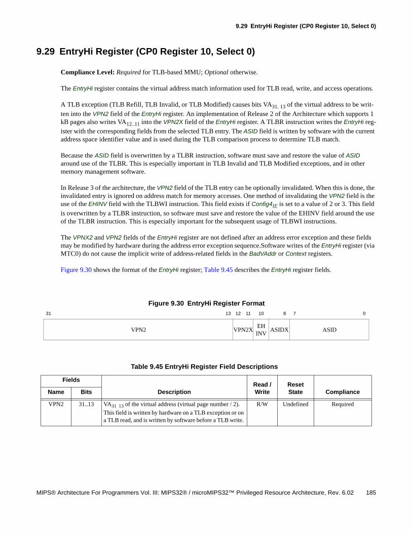
9.29 EntryHi Register (CP0 Register 10, Select 0)
MIPS® Architecture For Programmers Vol. III: MIPS32® / microMIPS32™ Privileged Resource Architecture, Rev. 6.02 185
9.29 EntryHi Register (CP0 Register 10, Select 0)
Compliance Level: Required for TLB-based MMU; Optional otherwise.
The EntryHi register contains the virtual address match information used for TLB read, write, and access operations.
A TLB exception (TLB Refill, TLB Invalid, or TLB Modified) causes bits VA31. 13 of the virtual address to be writ-
ten into the VPN2 field of the EntryHi register. An implementation of Release 2 of the Architecture which supports 1 kB pages also writes VA12..11 into the VPN2X field of the EntryHi register. A TLBR instruction writes the EntryHi reg-
ister with the corresponding fields from the selected TLB entry. The ASID field is written by software with the current address space identifier value and is used during the TLB comparison process to determine TLB match.
Because the ASID field is overwritten by a TLBR instruction, software must save and restore the value of ASID around use of the TLBR. This is especially important in TLB Invalid and TLB Modified exceptions, and in other memory management software.
In Release 3 of the architecture, the VPN2 field of the TLB entry can be optionally invalidated. When this is done, the invalidated entry is ignored on address match for memory accesses. One method of invalidating the VPN2 field is the use of the EHINV field with the TLBWI instruction. This field exists if Config4IE is set to a value of 2 or 3. This field
is overwritten by a TLBR instruction, so software must save and restore the value of the EHINV field around the use of the TLBR instruction. This is especially important for the subsequent usage of TLBWI instructions.
The VPNX2 and VPN2 fields of the EntryHi register are not defined after an address error exception and these fields may be modified by hardware during the address error exception sequence.Software writes of the EntryHi register (via MTC0) do not cause the implicit write of address-related fields in the BadVAddr or Context registers.
Figure 9.30 shows the format of the EntryHi register; Table 9.45 describes the EntryHi register fields.
Figure 9.30 EntryHi Register Format
31 13 12 11 10 8 7 0
VPN2 VPN2XEHINV
ASIDX ASID
Table 9.45 EntryHi Register Field Descriptions
Fields
DescriptionRead / Write
Reset State ComplianceName Bits
VPN2 31..13 VA31 13 of the virtual address (virtual page number / 2).
This field is written by hardware on a TLB exception or on a TLB read, and is written by software before a TLB write.
R/W Undefined Required
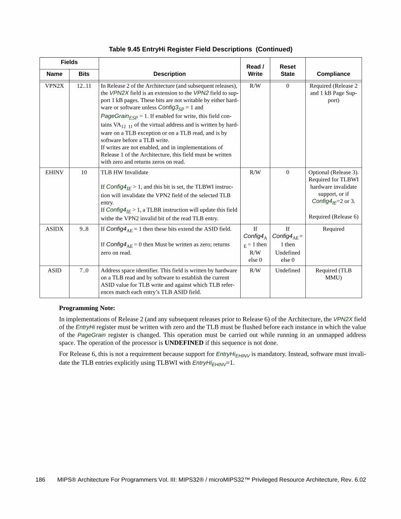
186 MIPS® Architecture For Programmers Vol. III: MIPS32® / microMIPS32™ Privileged Resource Architecture, Rev. 6.02
Programming Note:
In implementations of Release 2 (and any subsequent releases prior to Release 6) of the Architecture, the VPN2X fieldof the EntryHi register must be written with zero and the TLB must be flushed before each instance in which the valueof the PageGrain register is changed. This operation must be carried out while running in an unmapped addressspace. The operation of the processor is UNDEFINED if this sequence is not done.
For Release 6, this is not a requirement because support for EntryHiEHINV is mandatory. Instead, software must invali-date the TLB entries explicitly using TLBWI with EntryHiEHINV=1.
VPN2X 12..11 In Release 2 of the Architecture (and subsequent releases), the VPN2X field is an extension to the VPN2 field to sup-port 1 kB pages. These bits are not writable by either hard-ware or software unless Config3SP = 1 and
PageGrainESP = 1. If enabled for write, this field con-
tains VA12 11 of the virtual address and is written by hard-
ware on a TLB exception or on a TLB read, and is by software before a TLB write.If writes are not enabled, and in implementations of Release 1 of the Architecture, this field must be written with zero and returns zeros on read.
R/W 0 Required (Release 2 and 1 kB Page Sup-
port)
EHINV 10 TLB HW Invalidate
If Config4IE > 1, and this bit is set, the TLBWI instruc-
tion will invalidate the VPN2 field of the selected TLB entry. If Config4IE > 1, a TLBR instruction will update this field
withe the VPN2 invalid bit of the read TLB entry.
R/W 0 Optional (Release 3). Required for TLBWI hardware invalidate
support, or if Config4IE=2 or 3.
Required (Release 6)
ASIDX 9..8 If Config4AE = 1 then these bits extend the ASID field.
If Config4AE = 0 then Must be written as zero; returns
zero on read.
If Config4A
E = 1 then
R/Welse 0
If Config4AE =
1 then
Undefinedelse 0
Required
ASID 7..0 Address space identifier. This field is written by hardware on a TLB read and by software to establish the current ASID value for TLB write and against which TLB refer-ences match each entry’s TLB ASID field.
R/W Undefined Required (TLB MMU)
Table 9.45 EntryHi Register Field Descriptions (Continued)
Fields
DescriptionRead / Write
Reset State ComplianceName Bits
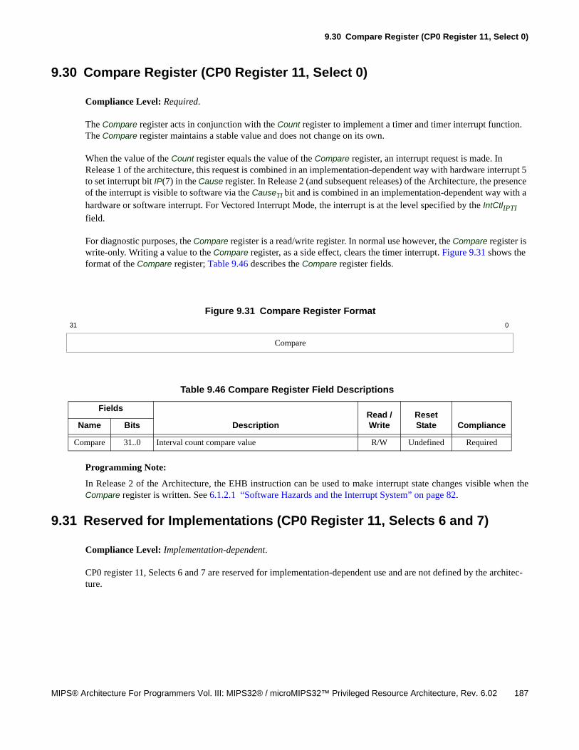
9.30 Compare Register (CP0 Register 11, Select 0)
MIPS® Architecture For Programmers Vol. III: MIPS32® / microMIPS32™ Privileged Resource Architecture, Rev. 6.02 187
9.30 Compare Register (CP0 Register 11, Select 0)
Compliance Level: Required.
The Compare register acts in conjunction with the Count register to implement a timer and timer interrupt function. The Compare register maintains a stable value and does not change on its own.
When the value of the Count register equals the value of the Compare register, an interrupt request is made. In Release 1 of the architecture, this request is combined in an implementation-dependent way with hardware interrupt 5 to set interrupt bit IP(7) in the Cause register. In Release 2 (and subsequent releases) of the Architecture, the presence of the interrupt is visible to software via the CauseTI bit and is combined in an implementation-dependent way with a hardware or software interrupt. For Vectored Interrupt Mode, the interrupt is at the level specified by the IntCtlIPTI
field.
For diagnostic purposes, the Compare register is a read/write register. In normal use however, the Compare register is write-only. Writing a value to the Compare register, as a side effect, clears the timer interrupt. Figure 9.31 shows the format of the Compare register; Table 9.46 describes the Compare register fields.
Programming Note:
In Release 2 of the Architecture, the EHB instruction can be used to make interrupt state changes visible when theCompare register is written. See 6.1.2.1 “Software Hazards and the Interrupt System” on page 82.
9.31 Reserved for Implementations (CP0 Register 11, Selects 6 and 7)
Compliance Level: Implementation-dependent.
CP0 register 11, Selects 6 and 7 are reserved for implementation-dependent use and are not defined by the architec-ture.
Figure 9.31 Compare Register Format
31 0
Compare
Table 9.46 Compare Register Field Descriptions
Fields
DescriptionRead / Write
Reset State ComplianceName Bits
Compare 31..0 Interval count compare value R/W Undefined Required

188 MIPS® Architecture For Programmers Vol. III: MIPS32® / microMIPS32™ Privileged Resource Architecture, Rev. 6.02
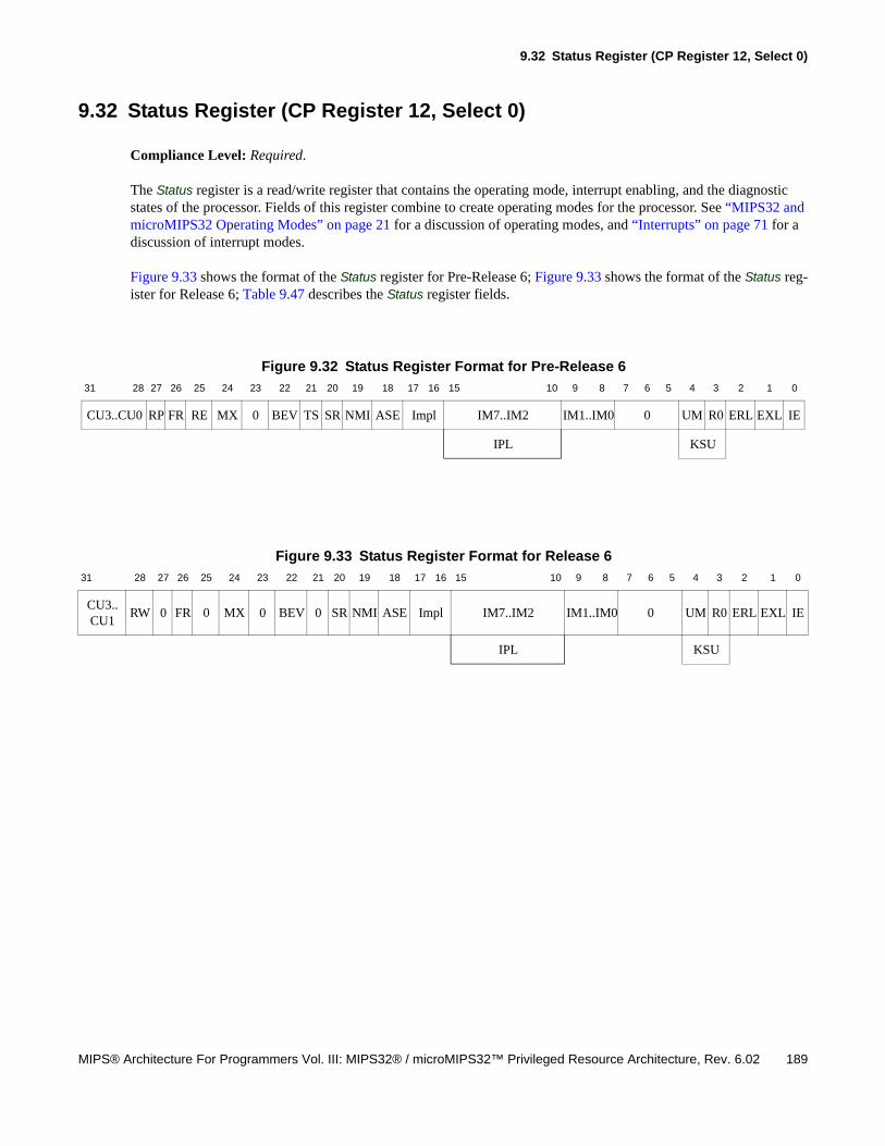
9.32 Status Register (CP Register 12, Select 0)
MIPS® Architecture For Programmers Vol. III: MIPS32® / microMIPS32™ Privileged Resource Architecture, Rev. 6.02 189
9.32 Status Register (CP Register 12, Select 0)
Compliance Level: Required.
The Status register is a read/write register that contains the operating mode, interrupt enabling, and the diagnostic states of the processor. Fields of this register combine to create operating modes for the processor. See “MIPS32 and microMIPS32 Operating Modes” on page 21 for a discussion of operating modes, and “Interrupts” on page 71 for a discussion of interrupt modes.
Figure 9.33 shows the format of the Status register for Pre-Release 6; Figure 9.33 shows the format of the Status reg-ister for Release 6; Table 9.47 describes the Status register fields.
Figure 9.32 Status Register Format for Pre-Release 6
31 28 27 26 25 24 23 22 21 20 19 18 17 16 15 10 9 8 7 6 5 4 3 2 1 0
CU3..CU0 RP FR RE MX 0 BEV TS SR NMI ASE Impl IM7..IM2 IM1..IM0 0 UM R0 ERL EXL IE
IPL KSU
Figure 9.33 Status Register Format for Release 6
31 28 27 26 25 24 23 22 21 20 19 18 17 16 15 10 9 8 7 6 5 4 3 2 1 0
CU3..CU1
RW 0 FR 0 MX 0 BEV 0 SR NMI ASE Impl IM7..IM2 IM1..IM0 0 UM R0 ERL EXL IE
IPL KSU
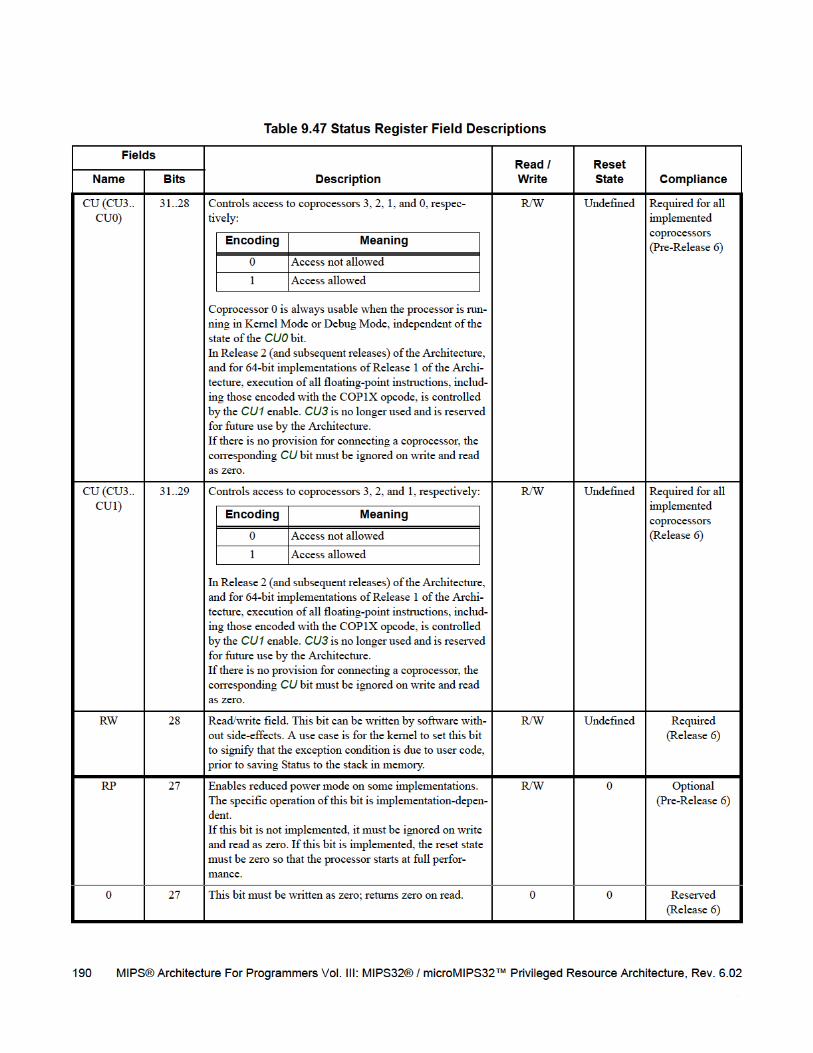
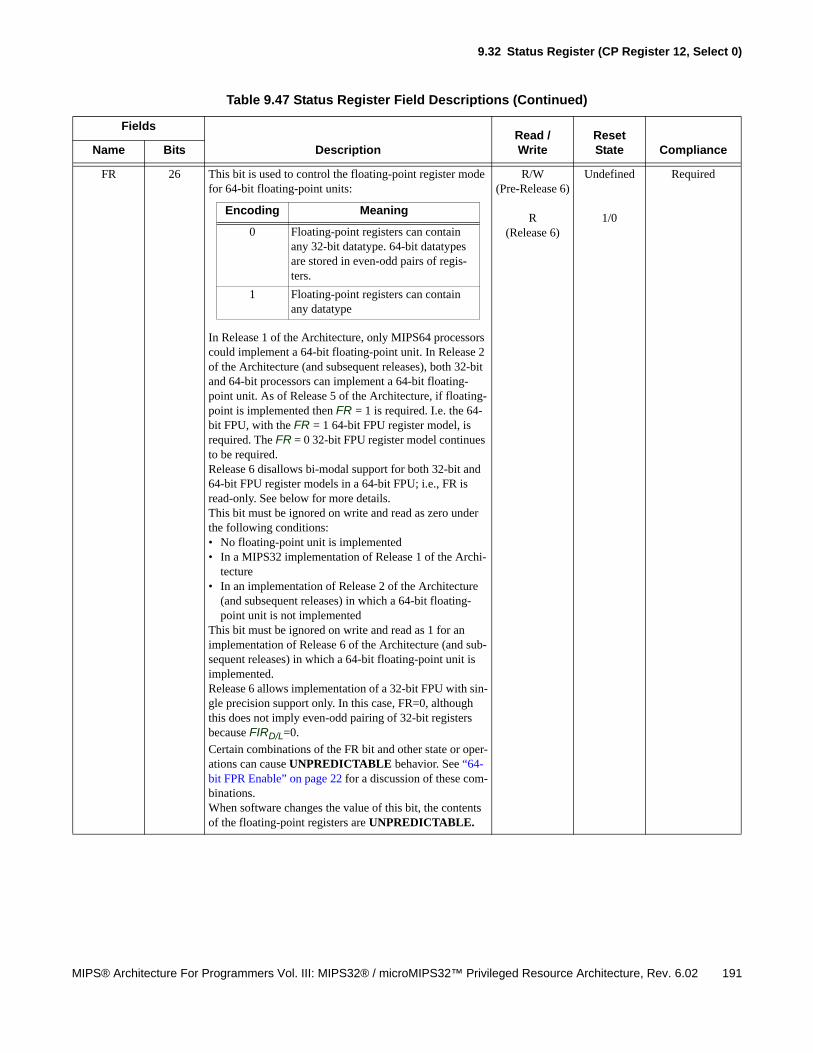
9.32 Status Register (CP Register 12, Select 0)
MIPS® Architecture For Programmers Vol. III: MIPS32® / microMIPS32™ Privileged Resource Architecture, Rev. 6.02 191
FR 26 This bit is used to control the floating-point register mode for 64-bit floating-point units:
In Release 1 of the Architecture, only MIPS64 processors could implement a 64-bit floating-point unit. In Release 2 of the Architecture (and subsequent releases), both 32-bit and 64-bit processors can implement a 64-bit floating-point unit. As of Release 5 of the Architecture, if floating-point is implemented then FR = 1 is required. I.e. the 64-bit FPU, with the FR = 1 64-bit FPU register model, is required. The FR = 0 32-bit FPU register model continues to be required.Release 6 disallows bi-modal support for both 32-bit and 64-bit FPU register models in a 64-bit FPU; i.e., FR is read-only. See below for more details.This bit must be ignored on write and read as zero under the following conditions:• No floating-point unit is implemented• In a MIPS32 implementation of Release 1 of the Archi-
tecture• In an implementation of Release 2 of the Architecture
(and subsequent releases) in which a 64-bit floating-point unit is not implemented
This bit must be ignored on write and read as 1 for an implementation of Release 6 of the Architecture (and sub-sequent releases) in which a 64-bit floating-point unit is implemented.Release 6 allows implementation of a 32-bit FPU with sin-gle precision support only. In this case, FR=0, although this does not imply even-odd pairing of 32-bit registers because FIRD/L=0.
Certain combinations of the FR bit and other state or oper-ations can cause UNPREDICTABLE behavior. See “64-bit FPR Enable” on page 22 for a discussion of these com-binations.When software changes the value of this bit, the contents of the floating-point registers are UNPREDICTABLE.
R/W(Pre-Release 6)
R(Release 6)
Undefined
1/0
Required
Table 9.47 Status Register Field Descriptions (Continued)
Fields
DescriptionRead /Write
Reset State ComplianceName Bits
Encoding Meaning
0 Floating-point registers can contain any 32-bit datatype. 64-bit datatypes are stored in even-odd pairs of regis-ters.
1 Floating-point registers can contain any datatype
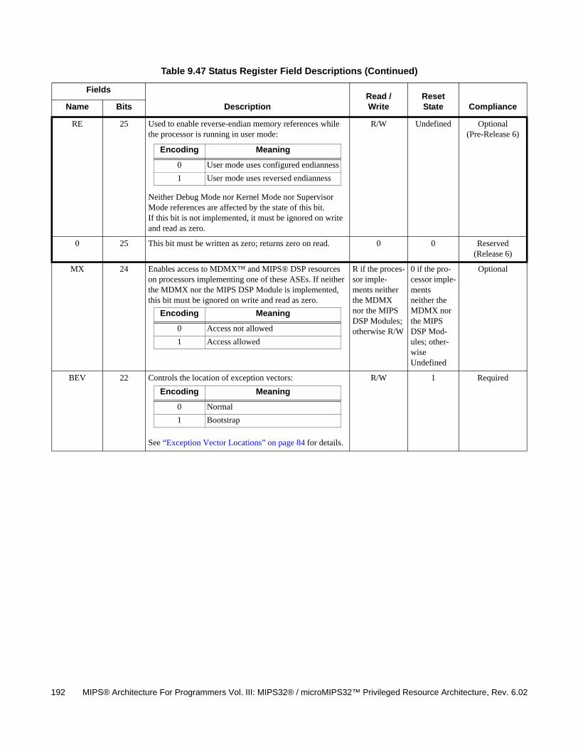
192 MIPS® Architecture For Programmers Vol. III: MIPS32® / microMIPS32™ Privileged Resource Architecture, Rev. 6.02
RE 25 Used to enable reverse-endian memory references while the processor is running in user mode:
Neither Debug Mode nor Kernel Mode nor Supervisor Mode references are affected by the state of this bit.If this bit is not implemented, it must be ignored on write and read as zero.
R/W Undefined Optional(Pre-Release 6)
0 25 This bit must be written as zero; returns zero on read. 0 0 Reserved (Release 6)
MX 24 Enables access to MDMX™ and MIPS® DSP resources on processors implementing one of these ASEs. If neither the MDMX nor the MIPS DSP Module is implemented, this bit must be ignored on write and read as zero.
R if the proces-sor imple-ments neither the MDMX nor the MIPS DSP Modules; otherwise R/W
0 if the pro-cessor imple-ments neither the MDMX nor the MIPS DSP Mod-ules; other-wise Undefined
Optional
BEV 22 Controls the location of exception vectors:
See “Exception Vector Locations” on page 84 for details.
R/W 1 Required
Table 9.47 Status Register Field Descriptions (Continued)
Fields
DescriptionRead /Write
Reset State ComplianceName Bits
Encoding Meaning
0 User mode uses configured endianness
1 User mode uses reversed endianness
Encoding Meaning
0 Access not allowed
1 Access allowed
Encoding Meaning
0 Normal
1 Bootstrap
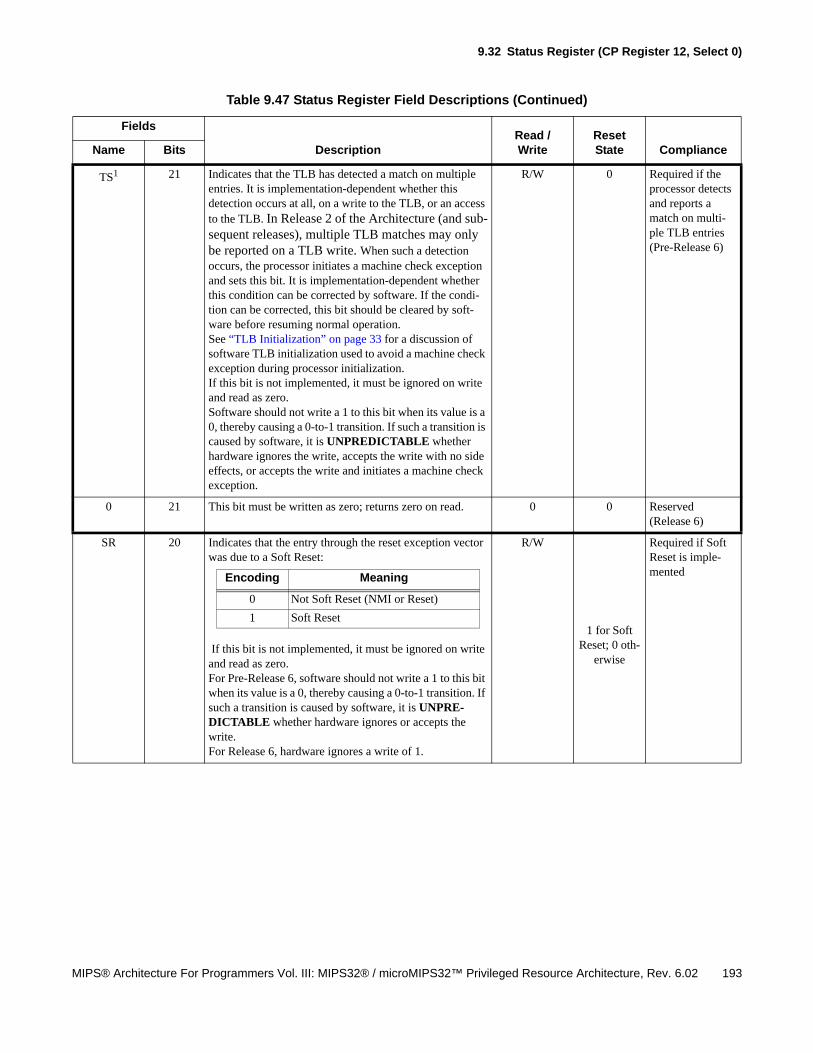
9.32 Status Register (CP Register 12, Select 0)
MIPS® Architecture For Programmers Vol. III: MIPS32® / microMIPS32™ Privileged Resource Architecture, Rev. 6.02 193
TS1 21 Indicates that the TLB has detected a match on multiple entries. It is implementation-dependent whether this detection occurs at all, on a write to the TLB, or an access to the TLB. In Release 2 of the Architecture (and sub-sequent releases), multiple TLB matches may only be reported on a TLB write. When such a detection occurs, the processor initiates a machine check exception and sets this bit. It is implementation-dependent whether this condition can be corrected by software. If the condi-tion can be corrected, this bit should be cleared by soft-ware before resuming normal operation.See “TLB Initialization” on page 33 for a discussion of software TLB initialization used to avoid a machine check exception during processor initialization.If this bit is not implemented, it must be ignored on write and read as zero.Software should not write a 1 to this bit when its value is a 0, thereby causing a 0-to-1 transition. If such a transition is caused by software, it is UNPREDICTABLE whether hardware ignores the write, accepts the write with no side effects, or accepts the write and initiates a machine check exception.
R/W 0 Required if the processor detects and reports a match on multi-ple TLB entries (Pre-Release 6)
0 21 This bit must be written as zero; returns zero on read. 0 0 Reserved (Release 6)
SR 20 Indicates that the entry through the reset exception vector was due to a Soft Reset:
If this bit is not implemented, it must be ignored on write and read as zero.For Pre-Release 6, software should not write a 1 to this bit when its value is a 0, thereby causing a 0-to-1 transition. If such a transition is caused by software, it is UNPRE-DICTABLE whether hardware ignores or accepts the write.For Release 6, hardware ignores a write of 1.
R/W
1 for Soft Reset; 0 oth-
erwise
Required if Soft Reset is imple-mented
Table 9.47 Status Register Field Descriptions (Continued)
Fields
DescriptionRead /Write
Reset State ComplianceName Bits
Encoding Meaning
0 Not Soft Reset (NMI or Reset)
1 Soft Reset
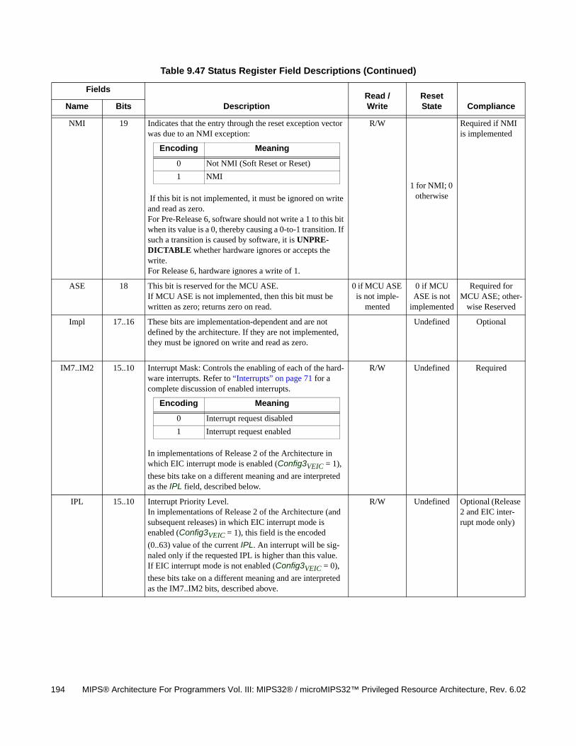
194 MIPS® Architecture For Programmers Vol. III: MIPS32® / microMIPS32™ Privileged Resource Architecture, Rev. 6.02
NMI 19 Indicates that the entry through the reset exception vector was due to an NMI exception:
If this bit is not implemented, it must be ignored on write and read as zero.For Pre-Release 6, software should not write a 1 to this bit when its value is a 0, thereby causing a 0-to-1 transition. If such a transition is caused by software, it is UNPRE-DICTABLE whether hardware ignores or accepts the write.For Release 6, hardware ignores a write of 1.
R/W
1 for NMI; 0 otherwise
Required if NMI is implemented
ASE 18 This bit is reserved for the MCU ASE. If MCU ASE is not implemented, then this bit must be written as zero; returns zero on read.
0 if MCU ASE is not imple-
mented
0 if MCU ASE is not
implemented
Required for MCU ASE; other-
wise Reserved
Impl 17..16 These bits are implementation-dependent and are not defined by the architecture. If they are not implemented, they must be ignored on write and read as zero.
Undefined Optional
IM7..IM2 15..10 Interrupt Mask: Controls the enabling of each of the hard-ware interrupts. Refer to “Interrupts” on page 71 for a complete discussion of enabled interrupts.
In implementations of Release 2 of the Architecture in which EIC interrupt mode is enabled (Config3VEIC = 1),
these bits take on a different meaning and are interpreted as the IPL field, described below.
R/W Undefined Required
IPL 15..10 Interrupt Priority Level.In implementations of Release 2 of the Architecture (and subsequent releases) in which EIC interrupt mode is enabled (Config3VEIC = 1), this field is the encoded
(0..63) value of the current IPL. An interrupt will be sig-naled only if the requested IPL is higher than this value.If EIC interrupt mode is not enabled (Config3VEIC = 0),
these bits take on a different meaning and are interpreted as the IM7..IM2 bits, described above.
R/W Undefined Optional (Release 2 and EIC inter-rupt mode only)
Table 9.47 Status Register Field Descriptions (Continued)
Fields
DescriptionRead /Write
Reset State ComplianceName Bits
Encoding Meaning
0 Not NMI (Soft Reset or Reset)
1 NMI
Encoding Meaning
0 Interrupt request disabled
1 Interrupt request enabled
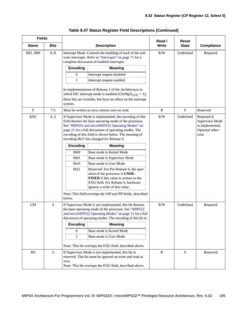
9.32 Status Register (CP Register 12, Select 0)
MIPS® Architecture For Programmers Vol. III: MIPS32® / microMIPS32™ Privileged Resource Architecture, Rev. 6.02 195
IM1..IM0 9..8 Interrupt Mask: Controls the enabling of each of the soft-ware interrupts. Refer to “Interrupts” on page 71 for a complete discussion of enabled interrupts.
In implementations of Release 2 of the Architecture in which EIC interrupt mode is enabled (Config3VEIC = 1),
these bits are writable, but have no effect on the interrupt system.
R/W Undefined Required
0 7:5 Must be written as zero; returns zero on read. R 0 Reserved
KSU 4..3 If Supervisor Mode is implemented, the encoding of this field denotes the base operating mode of the processor. See “MIPS32 and microMIPS32 Operating Modes” on page 21 for a full discussion of operating modes. The encoding of this field is shown below. The meaning of encoding 0b11 has changed for Release 6.
Note: This field overlaps the UM and R0 fields, described below.
R/W Undefined Required if Supervisor Mode is implemented; Optional other-wise
UM 4 If Supervisor Mode is not implemented, this bit denotes the base operating mode of the processor. See “MIPS32 and microMIPS32 Operating Modes” on page 21 for a full discussion of operating modes. The encoding of this bit is:
Note: This bit overlaps the KSU field, described above.
R/W Undefined Required
R0 3 If Supervisor Mode is not implemented, this bit is reserved. This bit must be ignored on write and read as zero.Note: This bit overlaps the KSU field, described above.
R 0 Reserved
Table 9.47 Status Register Field Descriptions (Continued)
Fields
DescriptionRead /Write
Reset State ComplianceName Bits
Encoding Meaning
0 Interrupt request disabled
1 Interrupt request enabled
Encoding Meaning
0b00 Base mode is Kernel Mode
0b01 Base mode is Supervisor Mode
0b10 Base mode is User Mode
0b11 Reserved. For Pre-Release 6, the oper-ation of the processor is UNDE-FINED if this value is written to the KSU field. For Release 6, hardware ignores a write of this value.
Encoding Meaning
0 Base mode is Kernel Mode
1 Base mode is User Mode
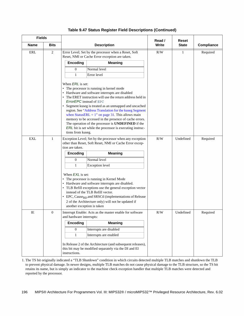
196 MIPS® Architecture For Programmers Vol. III: MIPS32® / microMIPS32™ Privileged Resource Architecture, Rev. 6.02
ERL 2 Error Level; Set by the processor when a Reset, Soft Reset, NMI or Cache Error exception are taken.
When ERL is set:• The processor is running in kernel mode• Hardware and software interrupts are disabled• The ERET instruction will use the return address held in
ErrorEPC instead of EPC• Segment kuseg is treated as an unmapped and uncached
region. See “Address Translation for the kuseg Segment when StatusERL = 1” on page 31. This allows main memory to be accessed in the presence of cache errors. The operation of the processor is UNDEFINED if the ERL bit is set while the processor is executing instruc-tions from kuseg.
R/W 1 Required
EXL 1 Exception Level; Set by the processor when any exception other than Reset, Soft Reset, NMI or Cache Error excep-tion are taken.
When EXL is set:• The processor is running in Kernel Mode• Hardware and software interrupts are disabled.• TLB Refill exceptions use the general exception vector
instead of the TLB Refill vector.• EPC, CauseBD and SRSCtl (implementations of Release
2 of the Architecture only) will not be updated if another exception is taken
R/W Undefined Required
IE 0 Interrupt Enable: Acts as the master enable for software and hardware interrupts:
In Release 2 of the Architecture (and subsequent releases), this bit may be modified separately via the DI and EI instructions.
R/W Undefined Required
1. The TS bit originally indicated a “TLB Shutdown” condition in which circuits detected multiple TLB matches and shutdown the TLB to prevent physical damage. In newer designs, multiple TLB matches do not cause physical damage to the TLB structure, so the TS bit retains its name, but is simply an indicator to the machine check exception handler that multiple TLB matches were detected and reported by the processor.
Table 9.47 Status Register Field Descriptions (Continued)
Fields
DescriptionRead /Write
Reset State ComplianceName Bits
Encoding Meaning
0 Normal level
1 Error level
Encoding Meaning
0 Normal level
1 Exception level
Encoding Meaning
0 Interrupts are disabled
1 Interrupts are enabled
9.32 Status Register (CP Register 12, Select 0)
MIPS® Architecture For Programmers Vol. III: MIPS32® / microMIPS32™ Privileged Resource Architecture, Rev. 6.02 197
Programming Note:
In Release 2 of the Architecture, the EHB instruction can be used to make interrupt state changes visible when the IM,IPL, ERL, EXL, or IE fields of the Status register are written. See “Software Hazards and the Interrupt System” onpage 82.

198 MIPS® Architecture For Programmers Vol. III: MIPS32® / microMIPS32™ Privileged Resource Architecture, Rev. 6.02
9.33 IntCtl Register (CP0 Register 12, Select 1)
MIPS® Architecture For Programmers Vol. III: MIPS32® / microMIPS32™ Privileged Resource Architecture, Rev. 6.02 199
9.33 IntCtl Register (CP0 Register 12, Select 1)
Compliance Level: Required (Release 2).
The IntCtl register controls the expanded interrupt capability added in Release 2 of the Architecture, including vec-tored interrupts and support for an external interrupt controller. This register does not exist in implementations of Release 1 of the Architecture.
Figure 9.34 shows the format of the IntCtl register; Table 9.48 describes the IntCtl register fields.
.
Figure 9.34 IntCtl Register Format
31 29 28 26 25 23 22 14 13 10 9 5 4 0
IPTI IPPCI IPFDC MCU ASE 0000 VS 0
Table 9.48 IntCtl Register Field Descriptions
Fields
DescriptionRead / Write
Reset State ComplianceName Bits
IPTI 31..29 For Interrupt Compatibility and Vectored Interrupt modes, this field specifies the IP number to which the Timer Inter-rupt request is merged, and allows software to determine whether to consider CauseTI for a potential interrupt.
The value of this field is UNPREDICTABLE if External Interrupt Controller Mode is both implemented and enabled. The external interrupt controller is expected to provide this information for that interrupt mode.
R Preset by hardware or Externally Set
Required
Encoding IP bitHardware
Interrupt Source
2 2 HW0
3 3 HW1
4 4 HW2
5 5 HW3
6 6 HW4
7 7 HW5
200 MIPS® Architecture For Programmers Vol. III: MIPS32® / microMIPS32™ Privileged Resource Architecture, Rev. 6.02
IPPCI 28..26 For Interrupt Compatibility and Vectored Interrupt modes, this field specifies the IP number to which the Perfor-mance Counter Interrupt request is merged, and allows software to determine whether to consider CausePCI for a
potential interrupt.
The value of this field is UNPREDICTABLE if External Interrupt Controller Mode is both implemented and enabled. The external interrupt controller is expected to provide this information for that interrupt mode.If performance counters are not implemented (Config1PC
= 0), this field returns zero on read.
R Preset by hardware or Externally Set
Optional (Per-formance Counters Implemented)
IPFDC 25..23 For Interrupt Compatibility and Vectored Interrupt modes, this field specifies the IP number to which the Fast Debug Channel Interrupt request is merged, and allows software to determine whether to consider CauseFDCI for a poten-
tial interrupt.
The value of this field is UNPREDICTABLE if External Interrupt Controller Mode is both implemented and enabled. The external interrupt controller is expected to provide this information for that interrupt mode.If EJTAG FDC is not implemented, this field returns zero on read.
R Preset by hardware or Externally Set
Optional (EJTAG Fast Debug Chan-nel Imple-mented)
MCU ASE 22..14 These bits are reserved for the MicroController ASE.
If that ASE is not implemented, must be written as zero; returns zero on read.
0 0 Reserved
Table 9.48 IntCtl Register Field Descriptions (Continued)
Fields
DescriptionRead / Write
Reset State ComplianceName Bits
Encoding IP bitHardware
Interrupt Source
2 2 HW0
3 3 HW1
4 4 HW2
5 5 HW3
6 6 HW4
7 7 HW5
Encoding IP bitHardware
Interrupt Source
2 2 HW0
3 3 HW1
4 4 HW2
5 5 HW3
6 6 HW4
7 7 HW5
9.33 IntCtl Register (CP0 Register 12, Select 1)
MIPS® Architecture For Programmers Vol. III: MIPS32® / microMIPS32™ Privileged Resource Architecture, Rev. 6.02 201
0 ..10 Must be written as zero; returns zero on read. 0 0 Reserved
VS 9..5 Vector Spacing. If vectored interrupts are implemented (as denoted by Config3VInt or Config3VEIC), this field speci-
fies the spacing between vectored interrupts.
All other values are reserved. For Pre-Release 6, the oper-ation of the processor is UNDEFINED if a reserved value is written to this field. For Release 6, hardware ignores writes of reserved values.If neither EIC interrupt mode nor VI mode are imple-mented (Config3VEIC = 0 and Config3VInt = 0), this field
is ignored on write and reads as zero.
R/W 0 Optional
0 4..0 Must be written as zero; returns zero on read. 0 0 Reserved
Table 9.48 IntCtl Register Field Descriptions (Continued)
Fields
DescriptionRead / Write
Reset State ComplianceName Bits
Encoding
Spacing Between Vectors
(hex) (decimal)
0x00 0x000 0
0x01 0x020 32
0x02 0x040 64
0x04 0x080 128
0x08 0x100 256
0x10 0x200 512

202 MIPS® Architecture For Programmers Vol. III: MIPS32® / microMIPS32™ Privileged Resource Architecture, Rev. 6.02
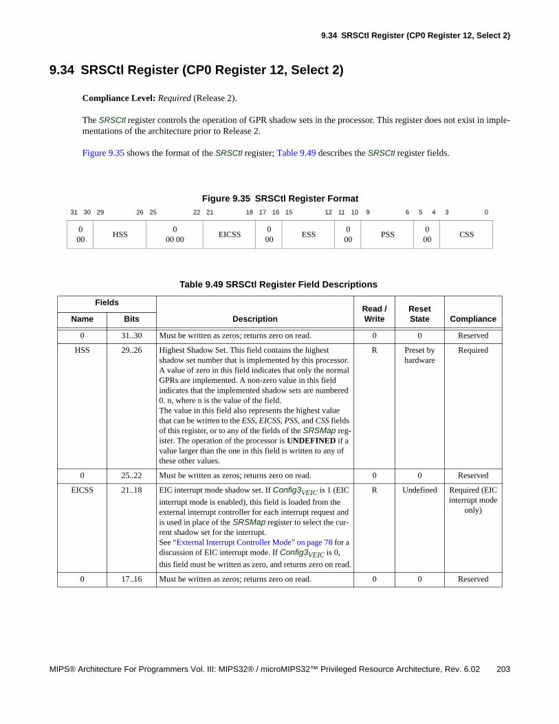
9.34 SRSCtl Register (CP0 Register 12, Select 2)
MIPS® Architecture For Programmers Vol. III: MIPS32® / microMIPS32™ Privileged Resource Architecture, Rev. 6.02 203
9.34 SRSCtl Register (CP0 Register 12, Select 2)
Compliance Level: Required (Release 2).
The SRSCtl register controls the operation of GPR shadow sets in the processor. This register does not exist in imple-mentations of the architecture prior to Release 2.
Figure 9.35 shows the format of the SRSCtl register; Table 9.49 describes the SRSCtl register fields.
Figure 9.35 SRSCtl Register Format
31 30 29 26 25 22 21 18 17 16 15 12 11 10 9 6 5 4 3 0
000
HSS0
00 00EICSS
000
ESS000
PSS000
CSS
Table 9.49 SRSCtl Register Field Descriptions
Fields
DescriptionRead / Write
Reset State ComplianceName Bits
0 31..30 Must be written as zeros; returns zero on read. 0 0 Reserved
HSS 29..26 Highest Shadow Set. This field contains the highest shadow set number that is implemented by this processor. A value of zero in this field indicates that only the normal GPRs are implemented. A non-zero value in this field indicates that the implemented shadow sets are numbered 0. n, where n is the value of the field.The value in this field also represents the highest value that can be written to the ESS, EICSS, PSS, and CSS fields of this register, or to any of the fields of the SRSMap reg-ister. The operation of the processor is UNDEFINED if a value larger than the one in this field is written to any of these other values.
R Preset by hardware
Required
0 25..22 Must be written as zeros; returns zero on read. 0 0 Reserved
EICSS 21..18 EIC interrupt mode shadow set. If Config3VEIC is 1 (EIC
interrupt mode is enabled), this field is loaded from the external interrupt controller for each interrupt request and is used in place of the SRSMap register to select the cur-rent shadow set for the interrupt.See “External Interrupt Controller Mode” on page 78 for a discussion of EIC interrupt mode. If Config3VEIC is 0,
this field must be written as zero, and returns zero on read.
R Undefined Required (EIC interrupt mode
only)
0 17..16 Must be written as zeros; returns zero on read. 0 0 Reserved
204 MIPS® Architecture For Programmers Vol. III: MIPS32® / microMIPS32™ Privileged Resource Architecture, Rev. 6.02
ESS 15..12 Exception Shadow Set. This field specifies the shadow set to use on entry to Kernel Mode caused by any exception other than a vectored interrupt.The operation of the processor is UNDEFINED if soft-ware writes a value into this field that is greater than the value in the HSS field.
R/W 0 Required
0 11..10 Must be written as zeros; returns zero on read. 0 0 Reserved
PSS 9..6 Previous Shadow Set. If GPR shadow registers are imple-mented, and with the exclusions noted in the next para-graph, this field is copied from the CSS field when an exception or interrupt occurs. An ERET instruction copies this value back into the CSS field if StatusBEV = 0.
This field is not updated on any exception which sets StatusERL to 1 (i.e., NMI or cache error), an entry into
EJTAG Debug mode, or any exception or interrupt that occurs with StatusEXL = 1, or StatusBEV = 1.
The operation of the processor is UNDEFINED if soft-ware writes a value into this field that is greater than the value in the HSS field.
R/W 0 Required
0 5..4 Must be written as zeros; returns zero on read. 0 0 Reserved
CSS 3..0 Current Shadow Set. If GPR shadow registers are imple-mented, this field is the number of the current GPR set. With the exclusions noted in the next paragraph, this field is updated with a new value on any interrupt or exception, and restored from the PSS field on an ERET. Table 9.50 describes the various sources from which the CSS field is updated on an exception or interrupt.This field is not updated on any exception which sets StatusERL to 1 (i.e., NMI or cache error), an entry into
EJTAG Debug mode, or any exception or interrupt that occurs with StatusEXL = 1, or StatusBEV = 1. Neither is it
updated on an ERET with StatusERL = 1 or StatusBEV =
1.The value of CSS can be changed directly by software only by writing the PSS field and executing an ERET instruction.
R 0 Required
Table 9.50 Sources for new SRSCtlCSS on an Exception or Interrupt
Exception Type Condition SRSCtlCSS Source Comment
Exception All SRSCtlESS
Non-Vectored Inter-rupt
CauseIV = 0 SRSCtlESS Treat as exception
Table 9.49 SRSCtl Register Field Descriptions (Continued)
Fields
DescriptionRead / Write
Reset State ComplianceName Bits
9.34 SRSCtl Register (CP0 Register 12, Select 2)
MIPS® Architecture For Programmers Vol. III: MIPS32® / microMIPS32™ Privileged Resource Architecture, Rev. 6.02 205
Programming Note:
A software change to the PSS field creates an instruction hazard between the write of the SRSCtl register and the useof a RDPGPR or WRPGPR instruction. This hazard must be cleared with a JR.HB or JALR.HB instruction asdescribed in “Hazard Clearing Instructions and Events” on page 107. A hardware change to the PSS field as the resultof interrupt or exception entry is automatically cleared for the execution of the first instruction in the interrupt orexception handler.
Vectored Interrupt CauseIV = 1 and
Config3VEIC = 0 and
Config3VInt = 1
SRSMapVectNum4+3..VectNum4
Source is internal map register
Vectored EIC Inter-rupt
CauseIV = 1 and
Config3VEIC = 1
SRSCtlEICSS Source is external interrupt controller.
Table 9.50 Sources for new SRSCtlCSS on an Exception or Interrupt (Continued)
Exception Type Condition SRSCtlCSS Source Comment

206 MIPS® Architecture For Programmers Vol. III: MIPS32® / microMIPS32™ Privileged Resource Architecture, Rev. 6.02
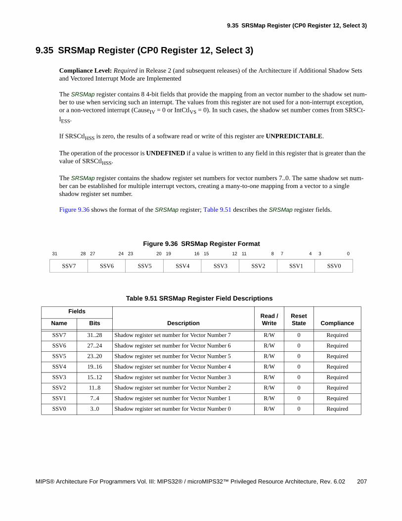
9.35 SRSMap Register (CP0 Register 12, Select 3)
MIPS® Architecture For Programmers Vol. III: MIPS32® / microMIPS32™ Privileged Resource Architecture, Rev. 6.02 207
9.35 SRSMap Register (CP0 Register 12, Select 3)
Compliance Level: Required in Release 2 (and subsequent releases) of the Architecture if Additional Shadow Sets and Vectored Interrupt Mode are Implemented
The SRSMap register contains 8 4-bit fields that provide the mapping from an vector number to the shadow set num-ber to use when servicing such an interrupt. The values from this register are not used for a non-interrupt exception, or a non-vectored interrupt (CauseIV = 0 or IntCtlVS = 0). In such cases, the shadow set number comes from SRSCt-
lESS.
If SRSCtlHSS is zero, the results of a software read or write of this register are UNPREDICTABLE.
The operation of the processor is UNDEFINED if a value is written to any field in this register that is greater than the value of SRSCtlHSS.
The SRSMap register contains the shadow register set numbers for vector numbers 7..0. The same shadow set num-ber can be established for multiple interrupt vectors, creating a many-to-one mapping from a vector to a single shadow register set number.
Figure 9.36 shows the format of the SRSMap register; Table 9.51 describes the SRSMap register fields.
Figure 9.36 SRSMap Register Format
31 28 27 24 23 20 19 16 15 12 11 8 7 4 3 0
SSV7 SSV6 SSV5 SSV4 SSV3 SSV2 SSV1 SSV0
Table 9.51 SRSMap Register Field Descriptions
Fields
DescriptionRead / Write
Reset State ComplianceName Bits
SSV7 31..28 Shadow register set number for Vector Number 7 R/W 0 Required
SSV6 27..24 Shadow register set number for Vector Number 6 R/W 0 Required
SSV5 23..20 Shadow register set number for Vector Number 5 R/W 0 Required
SSV4 19..16 Shadow register set number for Vector Number 4 R/W 0 Required
SSV3 15..12 Shadow register set number for Vector Number 3 R/W 0 Required
SSV2 11..8 Shadow register set number for Vector Number 2 R/W 0 Required
SSV1 7..4 Shadow register set number for Vector Number 1 R/W 0 Required
SSV0 3..0 Shadow register set number for Vector Number 0 R/W 0 Required

208 MIPS® Architecture For Programmers Vol. III: MIPS32® / microMIPS32™ Privileged Resource Architecture, Rev. 6.02
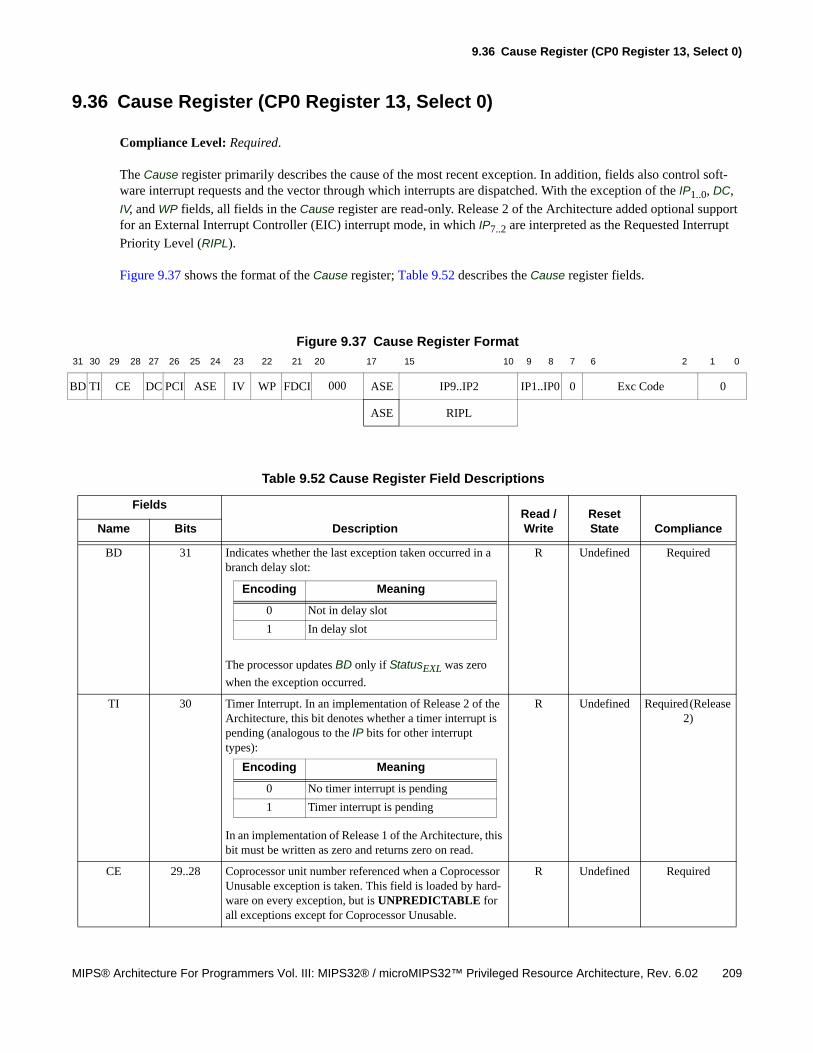
9.36 Cause Register (CP0 Register 13, Select 0)
MIPS® Architecture For Programmers Vol. III: MIPS32® / microMIPS32™ Privileged Resource Architecture, Rev. 6.02 209
9.36 Cause Register (CP0 Register 13, Select 0)
Compliance Level: Required.
The Cause register primarily describes the cause of the most recent exception. In addition, fields also control soft-ware interrupt requests and the vector through which interrupts are dispatched. With the exception of the IP1..0, DC,
IV, and WP fields, all fields in the Cause register are read-only. Release 2 of the Architecture added optional support for an External Interrupt Controller (EIC) interrupt mode, in which IP7..2 are interpreted as the Requested Interrupt
Priority Level (RIPL).
Figure 9.37 shows the format of the Cause register; Table 9.52 describes the Cause register fields.
Figure 9.37 Cause Register Format
31 30 29 28 27 26 25 24 23 22 21 20 17 15 10 9 8 7 6 2 1 0
BD TI CE DC PCI ASE IV WP FDCI 000 ASE IP9..IP2 IP1..IP0 0 Exc Code 0
ASE RIPL
Table 9.52 Cause Register Field Descriptions
Fields
DescriptionRead / Write
Reset State ComplianceName Bits
BD 31 Indicates whether the last exception taken occurred in a branch delay slot:
The processor updates BD only if StatusEXL was zero
when the exception occurred.
R Undefined Required
TI 30 Timer Interrupt. In an implementation of Release 2 of the Architecture, this bit denotes whether a timer interrupt is pending (analogous to the IP bits for other interrupt types):
In an implementation of Release 1 of the Architecture, this bit must be written as zero and returns zero on read.
R Undefined Required (Release 2)
CE 29..28 Coprocessor unit number referenced when a Coprocessor Unusable exception is taken. This field is loaded by hard-ware on every exception, but is UNPREDICTABLE for all exceptions except for Coprocessor Unusable.
R Undefined Required
Encoding Meaning
0 Not in delay slot
1 In delay slot
Encoding Meaning
0 No timer interrupt is pending
1 Timer interrupt is pending
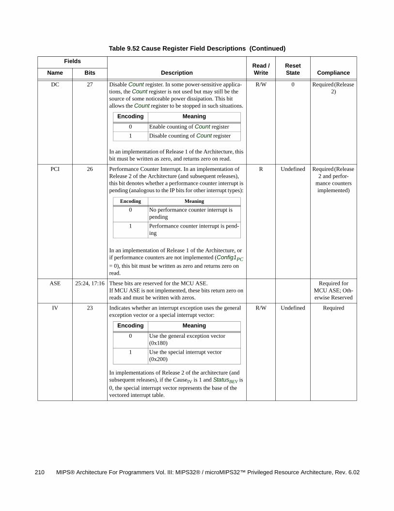
210 MIPS® Architecture For Programmers Vol. III: MIPS32® / microMIPS32™ Privileged Resource Architecture, Rev. 6.02
DC 27 Disable Count register. In some power-sensitive applica-tions, the Count register is not used but may still be the source of some noticeable power dissipation. This bit allows the Count register to be stopped in such situations.
In an implementation of Release 1 of the Architecture, this bit must be written as zero, and returns zero on read.
R/W 0 Required (Release 2)
PCI 26 Performance Counter Interrupt. In an implementation of Release 2 of the Architecture (and subsequent releases), this bit denotes whether a performance counter interrupt is pending (analogous to the IP bits for other interrupt types):
In an implementation of Release 1 of the Architecture, or if performance counters are not implemented (Config1PC
= 0), this bit must be written as zero and returns zero on read.
R Undefined Required (Release 2 and perfor-
mance counters implemented)
ASE 25:24, 17:16 These bits are reserved for the MCU ASE. If MCU ASE is not implemented, these bits return zero on reads and must be written with zeros.
Required for MCU ASE; Oth-erwise Reserved
IV 23 Indicates whether an interrupt exception uses the general exception vector or a special interrupt vector:
In implementations of Release 2 of the architecture (and subsequent releases), if the CauseIV is 1 and StatusBEV is
0, the special interrupt vector represents the base of the vectored interrupt table.
R/W Undefined Required
Table 9.52 Cause Register Field Descriptions (Continued)
Fields
DescriptionRead / Write
Reset State ComplianceName Bits
Encoding Meaning
0 Enable counting of Count register
1 Disable counting of Count register
Encoding Meaning
0 No performance counter interrupt is pending
1 Performance counter interrupt is pend-ing
Encoding Meaning
0 Use the general exception vector (0x180)
1 Use the special interrupt vector (0x200)
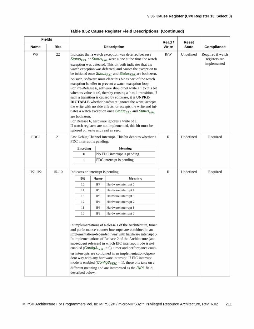
9.36 Cause Register (CP0 Register 13, Select 0)
MIPS® Architecture For Programmers Vol. III: MIPS32® / microMIPS32™ Privileged Resource Architecture, Rev. 6.02 211
WP 22 Indicates that a watch exception was deferred because StatusEXL or StatusERL were a one at the time the watch
exception was detected. This bit both indicates that the watch exception was deferred, and causes the exception to be initiated once StatusEXL and StatusERL are both zero.
As such, software must clear this bit as part of the watch exception handler to prevent a watch exception loop.For Pre-Release 6, software should not write a 1 to this bit when its value is a 0, thereby causing a 0-to-1 transition. If such a transition is caused by software, it is UNPRE-DICTABLE whether hardware ignores the write, accepts the write with no side effects, or accepts the write and ini-tiates a watch exception once StatusEXL and StatusERL
are both zero.For Release 6, hardware ignores a write of 1. If watch registers are not implemented, this bit must be ignored on write and read as zero.
R/W Undefined Required if watch registers are implemented
FDCI 21 Fast Debug Channel Interrupt. This bit denotes whether a FDC interrupt is pending:
R Undefined Required
IP7..IP2 15..10 Indicates an interrupt is pending:
In implementations of Release 1 of the Architecture, timer and performance-counter interrupts are combined in an implementation-dependent way with hardware interrupt 5.In implementations of Release 2 of the Architecture (and subsequent releases) in which EIC interrupt mode is not enabled (Config3VEIC = 0), timer and performance coun-
ter interrupts are combined in an implementation-depen-dent way with any hardware interrupt. If EIC interrupt mode is enabled (Config3VEIC = 1), these bits take on a
different meaning and are interpreted as the RIPL field, described below.
R Undefined Required
Table 9.52 Cause Register Field Descriptions (Continued)
Fields
DescriptionRead / Write
Reset State ComplianceName Bits
Encoding Meaning
0 No FDC interrupt is pending
1 FDC interrupt is pending
Bit Name Meaning
15 IP7 Hardware interrupt 5
14 IP6 Hardware interrupt 4
13 IP5 Hardware interrupt 3
12 IP4 Hardware interrupt 2
11 IP3 Hardware interrupt 1
10 IP2 Hardware interrupt 0
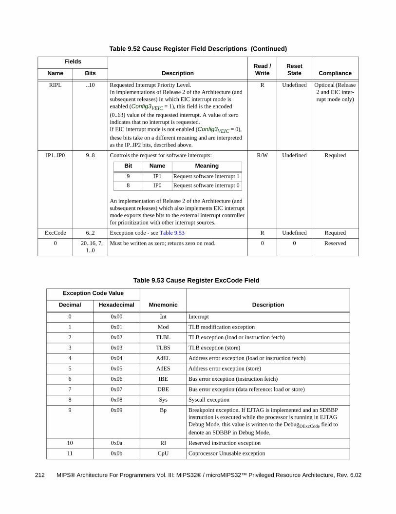
212 MIPS® Architecture For Programmers Vol. III: MIPS32® / microMIPS32™ Privileged Resource Architecture, Rev. 6.02
RIPL ..10 Requested Interrupt Priority Level.In implementations of Release 2 of the Architecture (and subsequent releases) in which EIC interrupt mode is enabled (Config3VEIC = 1), this field is the encoded
(0..63) value of the requested interrupt. A value of zero indicates that no interrupt is requested.If EIC interrupt mode is not enabled (Config3VEIC = 0),
these bits take on a different meaning and are interpreted as the IP..IP2 bits, described above.
R Undefined Optional (Release 2 and EIC inter-rupt mode only)
IP1..IP0 9..8 Controls the request for software interrupts:
An implementation of Release 2 of the Architecture (and subsequent releases) which also implements EIC interrupt mode exports these bits to the external interrupt controller for prioritization with other interrupt sources.
R/W Undefined Required
ExcCode 6..2 Exception code - see Table 9.53 R Undefined Required
0 20..16, 7, 1..0
Must be written as zero; returns zero on read. 0 0 Reserved
Table 9.53 Cause Register ExcCode Field
Exception Code Value
Mnemonic DescriptionDecimal Hexadecimal
0 0x00 Int Interrupt
1 0x01 Mod TLB modification exception
2 0x02 TLBL TLB exception (load or instruction fetch)
3 0x03 TLBS TLB exception (store)
4 0x04 AdEL Address error exception (load or instruction fetch)
5 0x05 AdES Address error exception (store)
6 0x06 IBE Bus error exception (instruction fetch)
7 0x07 DBE Bus error exception (data reference: load or store)
8 0x08 Sys Syscall exception
9 0x09 Bp Breakpoint exception. If EJTAG is implemented and an SDBBP instruction is executed while the processor is running in EJTAG Debug Mode, this value is written to the DebugDExcCode field to
denote an SDBBP in Debug Mode.
10 0x0a RI Reserved instruction exception
11 0x0b CpU Coprocessor Unusable exception
Table 9.52 Cause Register Field Descriptions (Continued)
Fields
DescriptionRead / Write
Reset State ComplianceName Bits
Bit Name Meaning
9 IP1 Request software interrupt 1
8 IP0 Request software interrupt 0
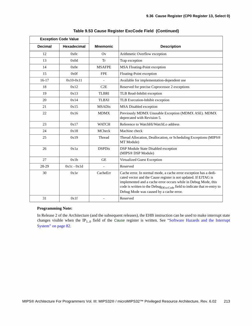
9.36 Cause Register (CP0 Register 13, Select 0)
MIPS® Architecture For Programmers Vol. III: MIPS32® / microMIPS32™ Privileged Resource Architecture, Rev. 6.02 213
Programming Note:
In Release 2 of the Architecture (and the subsequent releases), the EHB instruction can be used to make interrupt statechanges visible when the IP1..0 field of the Cause register is written. See “Software Hazards and the Interrupt
System” on page 82.
12 0x0c Ov Arithmetic Overflow exception
13 0x0d Tr Trap exception
14 0x0e MSAFPE MSA Floating-Point exception
15 0x0f FPE Floating-Point exception
16-17 0x10-0x11 - Available for implementation-dependent use
18 0x12 C2E Reserved for precise Coprocessor 2 exceptions
19 0x13 TLBRI TLB Read-Inhibit exception
20 0x14 TLBXI TLB Execution-Inhibit exception
21 0x15 MSADis MSA Disabled exception
22 0x16 MDMX Previously MDMX Unusable Exception (MDMX ASE). MDMX deprecated with Revision 5.
23 0x17 WATCH Reference to WatchHi/WatchLo address
24 0x18 MCheck Machine check
25 0x19 Thread Thread Allocation, Deallocation, or Scheduling Exceptions (MIPS® MT Module)
26 0x1a DSPDis DSP Module State Disabled exception(MIPS® DSP Module)
27 0x1b GE Virtualized Guest Exception
28-29 0x1c - 0x1d - Reserved
30 0x1e CacheErr Cache error. In normal mode, a cache error exception has a dedi-cated vector and the Cause register is not updated. If EJTAG is implemented and a cache error occurs while in Debug Mode, this code is written to the DebugDExcCode field to indicate that re-entry to
Debug Mode was caused by a cache error.
31 0x1f - Reserved
Table 9.53 Cause Register ExcCode Field (Continued)
Exception Code Value
Mnemonic DescriptionDecimal Hexadecimal

214 MIPS® Architecture For Programmers Vol. III: MIPS32® / microMIPS32™ Privileged Resource Architecture, Rev. 6.02
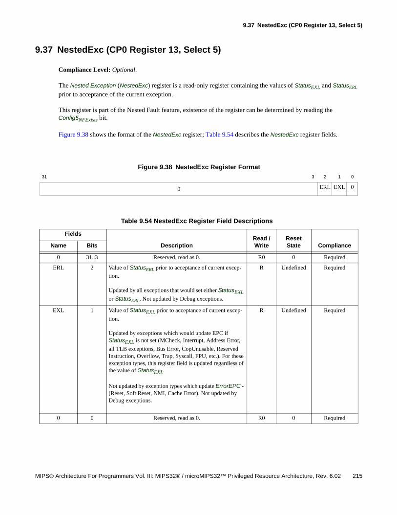
9.37 NestedExc (CP0 Register 13, Select 5)
MIPS® Architecture For Programmers Vol. III: MIPS32® / microMIPS32™ Privileged Resource Architecture, Rev. 6.02 215
9.37 NestedExc (CP0 Register 13, Select 5)
Compliance Level: Optional.
The Nested Exception (NestedExc) register is a read-only register containing the values of StatusEXL and StatusERL
prior to acceptance of the current exception.
This register is part of the Nested Fault feature, existence of the register can be determined by reading the Config5NFExists bit.
Figure 9.38 shows the format of the NestedExc register; Table 9.54 describes the NestedExc register fields.
Figure 9.38 NestedExc Register Format
31 3 2 1 0
0 ERL EXL 0
Table 9.54 NestedExc Register Field Descriptions
Fields
DescriptionRead / Write
Reset State ComplianceName Bits
0 31..3 Reserved, read as 0. R0 0 Required
ERL 2 Value of StatusERL prior to acceptance of current excep-
tion.
Updated by all exceptions that would set either StatusEXL
or StatusERL. Not updated by Debug exceptions.
R Undefined Required
EXL 1 Value of StatusEXL prior to acceptance of current excep-
tion.
Updated by exceptions which would update EPC if StatusEXL is not set (MCheck, Interrupt, Address Error,
all TLB exceptions, Bus Error, CopUnusable, Reserved Instruction, Overflow, Trap, Syscall, FPU, etc.). For these exception types, this register field is updated regardless of the value of StatusEXL.
Not updated by exception types which update ErrorEPC - (Reset, Soft Reset, NMI, Cache Error). Not updated by Debug exceptions.
R Undefined Required
0 0 Reserved, read as 0. R0 0 Required

216 MIPS® Architecture For Programmers Vol. III: MIPS32® / microMIPS32™ Privileged Resource Architecture, Rev. 6.02
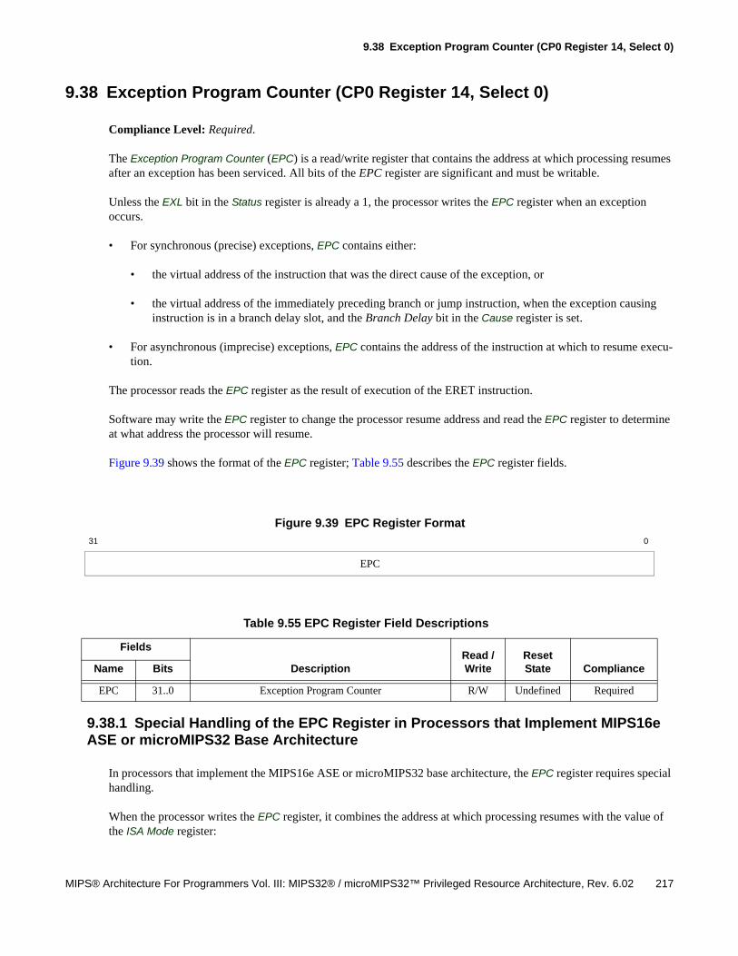
9.38 Exception Program Counter (CP0 Register 14, Select 0)
MIPS® Architecture For Programmers Vol. III: MIPS32® / microMIPS32™ Privileged Resource Architecture, Rev. 6.02 217
9.38 Exception Program Counter (CP0 Register 14, Select 0)
Compliance Level: Required.
The Exception Program Counter (EPC) is a read/write register that contains the address at which processing resumes after an exception has been serviced. All bits of the EPC register are significant and must be writable.
Unless the EXL bit in the Status register is already a 1, the processor writes the EPC register when an exception occurs.
• For synchronous (precise) exceptions, EPC contains either:
• the virtual address of the instruction that was the direct cause of the exception, or
• the virtual address of the immediately preceding branch or jump instruction, when the exception causing instruction is in a branch delay slot, and the Branch Delay bit in the Cause register is set.
• For asynchronous (imprecise) exceptions, EPC contains the address of the instruction at which to resume execu-tion.
The processor reads the EPC register as the result of execution of the ERET instruction.
Software may write the EPC register to change the processor resume address and read the EPC register to determine at what address the processor will resume.
Figure 9.39 shows the format of the EPC register; Table 9.55 describes the EPC register fields.
9.38.1 Special Handling of the EPC Register in Processors that Implement MIPS16e ASE or microMIPS32 Base Architecture
In processors that implement the MIPS16e ASE or microMIPS32 base architecture, the EPC register requires special handling.
When the processor writes the EPC register, it combines the address at which processing resumes with the value of the ISA Mode register:
Figure 9.39 EPC Register Format
31 0
EPC
Table 9.55 EPC Register Field Descriptions
Fields
DescriptionRead / Write
Reset State ComplianceName Bits
EPC 31..0 Exception Program Counter R/W Undefined Required
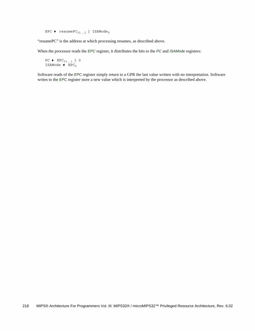
218 MIPS® Architecture For Programmers Vol. III: MIPS32® / microMIPS32™ Privileged Resource Architecture, Rev. 6.02
EPC resumePC31..1 ISAMode0
“resumePC” is the address at which processing resumes, as described above.
When the processor reads the EPC register, it distributes the bits to the PC and ISAMode registers:
PC EPC31..1 0ISAMode EPC0
Software reads of the EPC register simply return to a GPR the last value written with no interpretation. Software writes to the EPC register store a new value which is interpreted by the processor as described above.
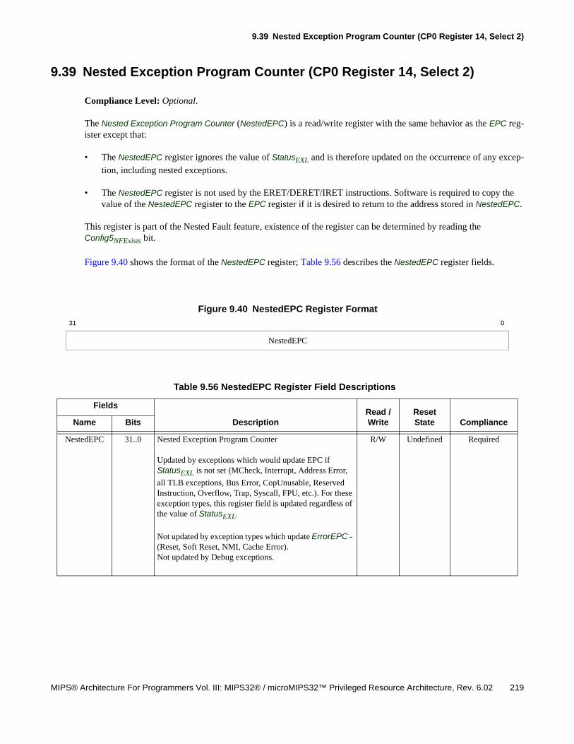
9.39 Nested Exception Program Counter (CP0 Register 14, Select 2)
MIPS® Architecture For Programmers Vol. III: MIPS32® / microMIPS32™ Privileged Resource Architecture, Rev. 6.02 219
9.39 Nested Exception Program Counter (CP0 Register 14, Select 2)
Compliance Level: Optional.
The Nested Exception Program Counter (NestedEPC) is a read/write register with the same behavior as the EPC reg-ister except that:
• The NestedEPC register ignores the value of StatusEXL and is therefore updated on the occurrence of any excep-
tion, including nested exceptions.
• The NestedEPC register is not used by the ERET/DERET/IRET instructions. Software is required to copy the value of the NestedEPC register to the EPC register if it is desired to return to the address stored in NestedEPC.
This register is part of the Nested Fault feature, existence of the register can be determined by reading the Config5NFExists bit.
Figure 9.40 shows the format of the NestedEPC register; Table 9.56 describes the NestedEPC register fields.
Figure 9.40 NestedEPC Register Format
31 0
NestedEPC
Table 9.56 NestedEPC Register Field Descriptions
Fields
DescriptionRead / Write
Reset State ComplianceName Bits
NestedEPC 31..0 Nested Exception Program Counter
Updated by exceptions which would update EPC if StatusEXL is not set (MCheck, Interrupt, Address Error,
all TLB exceptions, Bus Error, CopUnusable, Reserved Instruction, Overflow, Trap, Syscall, FPU, etc.). For these exception types, this register field is updated regardless of the value of StatusEXL.
Not updated by exception types which update ErrorEPC - (Reset, Soft Reset, NMI, Cache Error). Not updated by Debug exceptions.
R/W Undefined Required

220 MIPS® Architecture For Programmers Vol. III: MIPS32® / microMIPS32™ Privileged Resource Architecture, Rev. 6.02
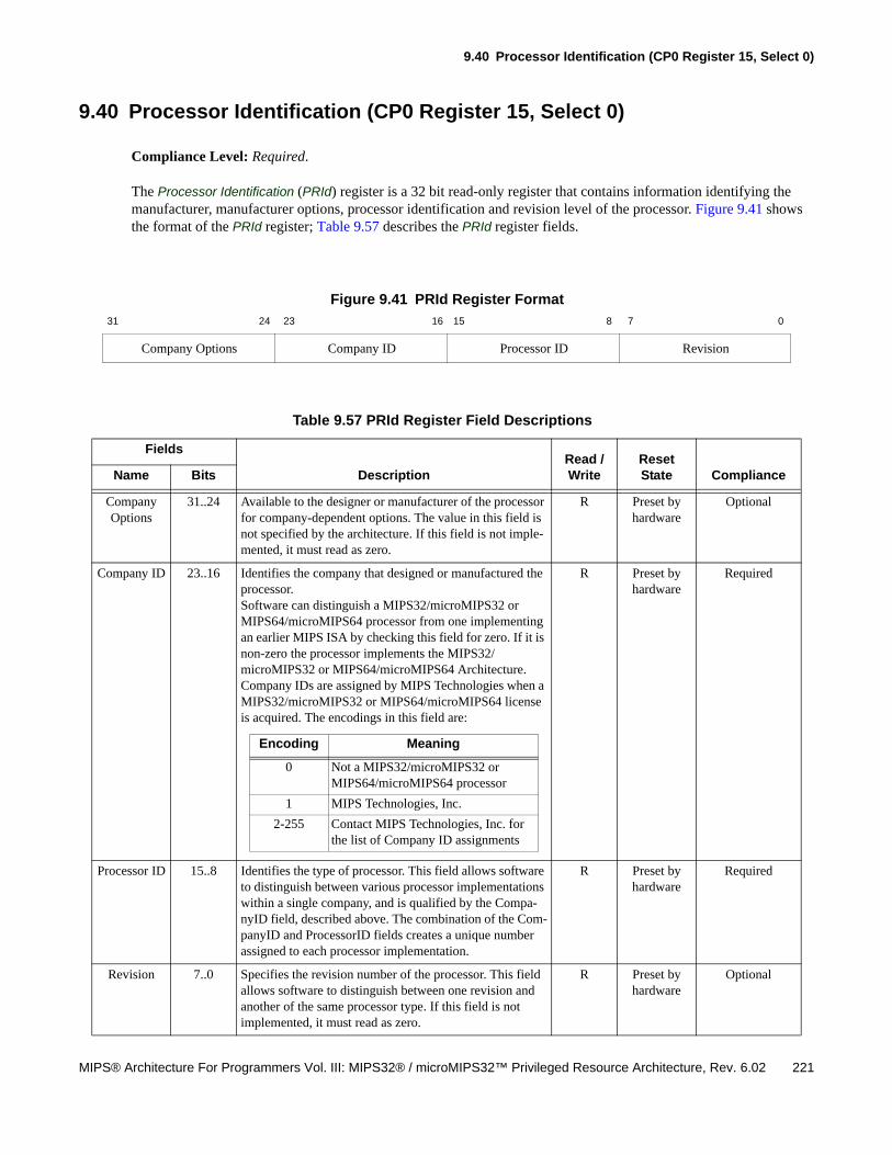
9.40 Processor Identification (CP0 Register 15, Select 0)
MIPS® Architecture For Programmers Vol. III: MIPS32® / microMIPS32™ Privileged Resource Architecture, Rev. 6.02 221
9.40 Processor Identification (CP0 Register 15, Select 0)
Compliance Level: Required.
The Processor Identification (PRId) register is a 32 bit read-only register that contains information identifying the manufacturer, manufacturer options, processor identification and revision level of the processor. Figure 9.41 shows the format of the PRId register; Table 9.57 describes the PRId register fields.
Figure 9.41 PRId Register Format
31 24 23 16 15 8 7 0
Company Options Company ID Processor ID Revision
Table 9.57 PRId Register Field Descriptions
Fields
DescriptionRead / Write
Reset State ComplianceName Bits
Company Options
31..24 Available to the designer or manufacturer of the processor for company-dependent options. The value in this field is not specified by the architecture. If this field is not imple-mented, it must read as zero.
R Preset by hardware
Optional
Company ID 23..16 Identifies the company that designed or manufactured the processor.Software can distinguish a MIPS32/microMIPS32 or MIPS64/microMIPS64 processor from one implementing an earlier MIPS ISA by checking this field for zero. If it is non-zero the processor implements the MIPS32/microMIPS32 or MIPS64/microMIPS64 Architecture.Company IDs are assigned by MIPS Technologies when a MIPS32/microMIPS32 or MIPS64/microMIPS64 license is acquired. The encodings in this field are:
R Preset by hardware
Required
Processor ID 15..8 Identifies the type of processor. This field allows software to distinguish between various processor implementations within a single company, and is qualified by the Compa-nyID field, described above. The combination of the Com-panyID and ProcessorID fields creates a unique number assigned to each processor implementation.
R Preset by hardware
Required
Revision 7..0 Specifies the revision number of the processor. This field allows software to distinguish between one revision and another of the same processor type. If this field is not implemented, it must read as zero.
R Preset by hardware
Optional
Encoding Meaning
0 Not a MIPS32/microMIPS32 or MIPS64/microMIPS64 processor
1 MIPS Technologies, Inc.
2-255 Contact MIPS Technologies, Inc. for the list of Company ID assignments
222 MIPS® Architecture For Programmers Vol. III: MIPS32® / microMIPS32™ Privileged Resource Architecture, Rev. 6.02
Software should not use the fields of this register to infer configuration information about the processor. Rather, the configuration registers should be used to determine the capabilities of the processor. Programmers who identify cases in which the configuration registers are not sufficient, requiring them to revert to check on the PRId register value, should send email to [email protected], reporting the specific case.
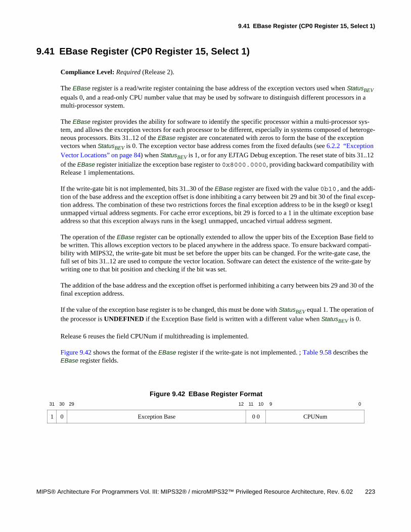
9.41 EBase Register (CP0 Register 15, Select 1)
MIPS® Architecture For Programmers Vol. III: MIPS32® / microMIPS32™ Privileged Resource Architecture, Rev. 6.02 223
9.41 EBase Register (CP0 Register 15, Select 1)
Compliance Level: Required (Release 2).
The EBase register is a read/write register containing the base address of the exception vectors used when StatusBEV
equals 0, and a read-only CPU number value that may be used by software to distinguish different processors in a multi-processor system.
The EBase register provides the ability for software to identify the specific processor within a multi-processor sys-tem, and allows the exception vectors for each processor to be different, especially in systems composed of heteroge-neous processors. Bits 31..12 of the EBase register are concatenated with zeros to form the base of the exception vectors when StatusBEV is 0. The exception vector base address comes from the fixed defaults (see 6.2.2 “Exception
Vector Locations” on page 84) when StatusBEV is 1, or for any EJTAG Debug exception. The reset state of bits 31..12
of the EBase register initialize the exception base register to 0x8000.0000, providing backward compatibility with Release 1 implementations.
If the write-gate bit is not implemented, bits 31..30 of the EBase register are fixed with the value 0b10,and the addi-tion of the base address and the exception offset is done inhibiting a carry between bit 29 and bit 30 of the final excep-tion address. The combination of these two restrictions forces the final exception address to be in the kseg0 or kseg1 unmapped virtual address segments. For cache error exceptions, bit 29 is forced to a 1 in the ultimate exception base address so that this exception always runs in the kseg1 unmapped, uncached virtual address segment.
The operation of the EBase register can be optionally extended to allow the upper bits of the Exception Base field to be written. This allows exception vectors to be placed anywhere in the address space. To ensure backward compati-bility with MIPS32, the write-gate bit must be set before the upper bits can be changed. For the write-gate case, the full set of bits 31..12 are used to compute the vector location. Software can detect the existence of the write-gate by writing one to that bit position and checking if the bit was set.
The addition of the base address and the exception offset is performed inhibiting a carry between bits 29 and 30 of the final exception address.
If the value of the exception base register is to be changed, this must be done with StatusBEV equal 1. The operation of
the processor is UNDEFINED if the Exception Base field is written with a different value when StatusBEV is 0.
Release 6 reuses the field CPUNum if multithreading is implemented.
Figure 9.42 shows the format of the EBase register if the write-gate is not implemented. ; Table 9.58 describes the EBase register fields.
Figure 9.42 EBase Register Format
31 30 29 12 11 10 9 0
1 0 Exception Base 0 0 CPUNum
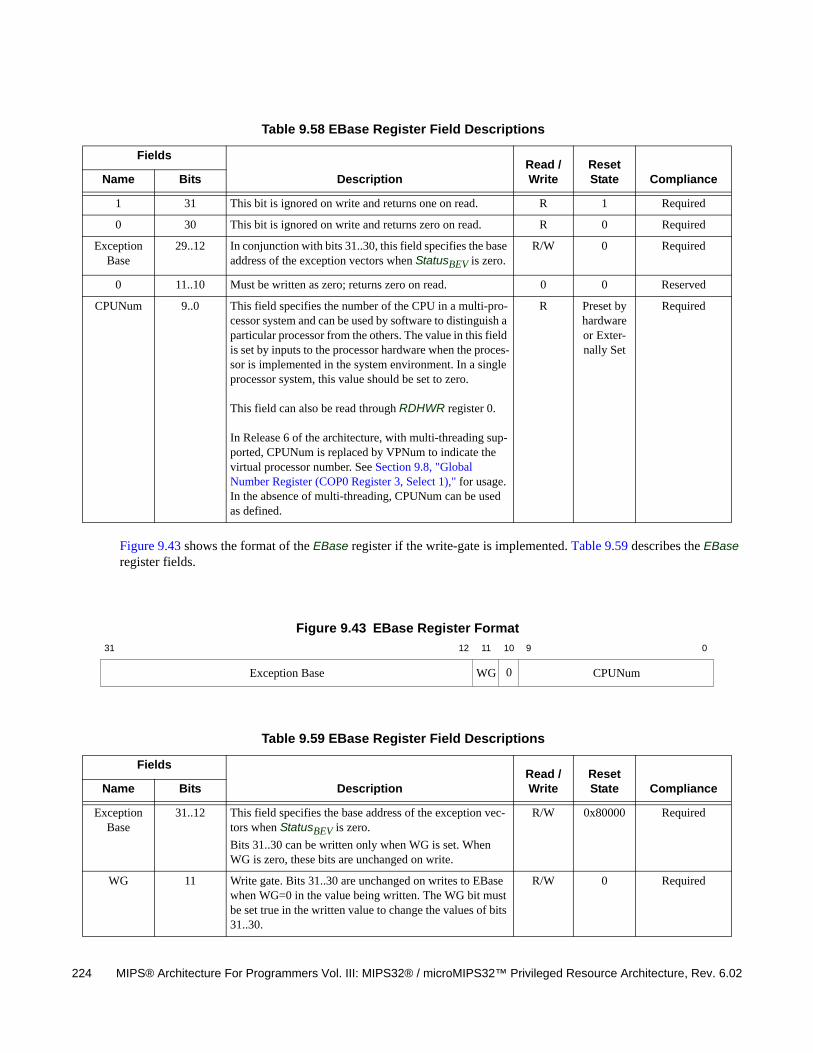
224 MIPS® Architecture For Programmers Vol. III: MIPS32® / microMIPS32™ Privileged Resource Architecture, Rev. 6.02
Figure 9.43 shows the format of the EBase register if the write-gate is implemented. Table 9.59 describes the EBase register fields.
Table 9.58 EBase Register Field Descriptions
Fields
DescriptionRead / Write
Reset State ComplianceName Bits
1 31 This bit is ignored on write and returns one on read. R 1 Required
0 30 This bit is ignored on write and returns zero on read. R 0 Required
Exception Base
29..12 In conjunction with bits 31..30, this field specifies the base address of the exception vectors when StatusBEV is zero.
R/W 0 Required
0 11..10 Must be written as zero; returns zero on read. 0 0 Reserved
CPUNum 9..0 This field specifies the number of the CPU in a multi-pro-cessor system and can be used by software to distinguish a particular processor from the others. The value in this field is set by inputs to the processor hardware when the proces-sor is implemented in the system environment. In a single processor system, this value should be set to zero.
This field can also be read through RDHWR register 0.
In Release 6 of the architecture, with multi-threading sup-ported, CPUNum is replaced by VPNum to indicate the virtual processor number. See Section 9.8, "Global Number Register (COP0 Register 3, Select 1)," for usage. In the absence of multi-threading, CPUNum can be used as defined.
R Preset by hardware or Exter-nally Set
Required
Figure 9.43 EBase Register Format
31 12 11 10 9 0
Exception Base WG 0 CPUNum
Table 9.59 EBase Register Field Descriptions
Fields
DescriptionRead / Write
Reset State ComplianceName Bits
Exception Base
31..12 This field specifies the base address of the exception vec-tors when StatusBEV is zero.
Bits 31..30 can be written only when WG is set. When WG is zero, these bits are unchanged on write.
R/W 0x80000 Required
WG 11 Write gate. Bits 31..30 are unchanged on writes to EBase when WG=0 in the value being written. The WG bit must be set true in the written value to change the values of bits 31..30.
R/W 0 Required
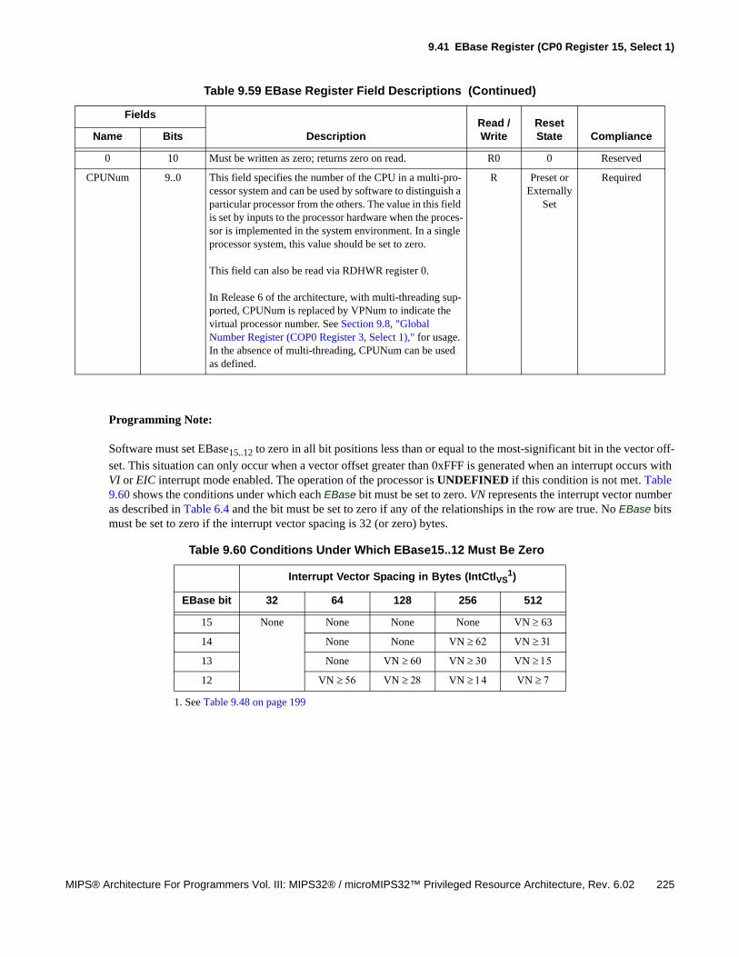
9.41 EBase Register (CP0 Register 15, Select 1)
MIPS® Architecture For Programmers Vol. III: MIPS32® / microMIPS32™ Privileged Resource Architecture, Rev. 6.02 225
Programming Note:
Software must set EBase15..12 to zero in all bit positions less than or equal to the most-significant bit in the vector off-
set. This situation can only occur when a vector offset greater than 0xFFF is generated when an interrupt occurs with VI or EIC interrupt mode enabled. The operation of the processor is UNDEFINED if this condition is not met. Table 9.60 shows the conditions under which each EBase bit must be set to zero. VN represents the interrupt vector number as described in Table 6.4 and the bit must be set to zero if any of the relationships in the row are true. No EBase bits must be set to zero if the interrupt vector spacing is 32 (or zero) bytes.
0 10 Must be written as zero; returns zero on read. R0 0 Reserved
CPUNum 9..0 This field specifies the number of the CPU in a multi-pro-cessor system and can be used by software to distinguish a particular processor from the others. The value in this field is set by inputs to the processor hardware when the proces-sor is implemented in the system environment. In a single processor system, this value should be set to zero.
This field can also be read via RDHWR register 0.
In Release 6 of the architecture, with multi-threading sup-ported, CPUNum is replaced by VPNum to indicate the virtual processor number. See Section 9.8, "Global Number Register (COP0 Register 3, Select 1)," for usage. In the absence of multi-threading, CPUNum can be used as defined.
R Preset or Externally
Set
Required
Table 9.60 Conditions Under Which EBase15..12 Must Be Zero
Interrupt Vector Spacing in Bytes (IntCtlVS1)
1. See Table 9.48 on page 199
EBase bit 32 64 128 256 512
15 None None None None VN 63
14 None None VN VN
13 None VN VN VN
12 VN VN VN VN
Table 9.59 EBase Register Field Descriptions (Continued)
Fields
DescriptionRead / Write
Reset State ComplianceName Bits

226 MIPS® Architecture For Programmers Vol. III: MIPS32® / microMIPS32™ Privileged Resource Architecture, Rev. 6.02
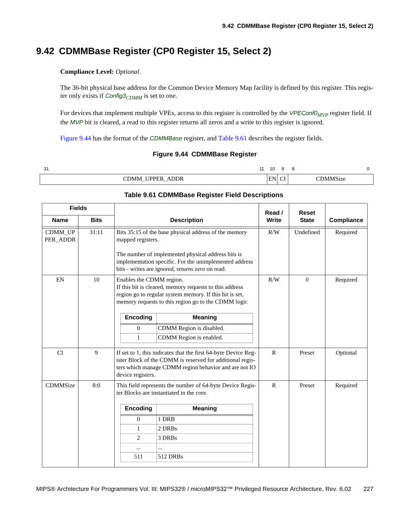
9.42 CDMMBase Register (CP0 Register 15, Select 2)
MIPS® Architecture For Programmers Vol. III: MIPS32® / microMIPS32™ Privileged Resource Architecture, Rev. 6.02 227
9.42 CDMMBase Register (CP0 Register 15, Select 2)
Compliance Level: Optional.
The 36-bit physical base address for the Common Device Memory Map facility is defined by this register. This regis-ter only exists if Config3CDMM is set to one.
For devices that implement multiple VPEs, access to this register is controlled by the VPEConf0MVP register field. If
the MVP bit is cleared, a read to this register returns all zeros and a write to this register is ignored.
Figure 9.44 has the format of the CDMMBase register, and Table 9.61 describes the register fields.
Figure 9.44 CDMMBase Register
31 11 10 9 8 0
CDMM_UPPER_ADDR EN CI CDMMSize
Table 9.61 CDMMBase Register Field Descriptions
Fields
DescriptionRead / Write
Reset State ComplianceName Bits
CDMM_UPPER_ADDR
31:11 Bits 35:15 of the base physical address of the memory mapped registers.
The number of implemented physical address bits is implementation specific. For the unimplemented address bits - writes are ignored, returns zero on read.
R/W Undefined Required
EN 10 Enables the CDMM region. If this bit is cleared, memory requests to this address region go to regular system memory. If this bit is set, memory requests to this region go to the CDMM logic
R/W 0 Required
CI 9 If set to 1, this indicates that the first 64-byte Device Reg-ister Block of the CDMM is reserved for additional regis-ters which manage CDMM region behavior and are not IO device registers.
R Preset Optional
CDMMSize 8:0 This field represents the number of 64-byte Device Regis-ter Blocks are instantiated in the core.
R Preset Required
Encoding Meaning
0 CDMM Region is disabled.
1 CDMM Region is enabled.
Encoding Meaning
0 1 DRB
1 2 DRBs
2 3 DRBs
... ...
511 512 DRBs

228 MIPS® Architecture For Programmers Vol. III: MIPS32® / microMIPS32™ Privileged Resource Architecture, Rev. 6.02
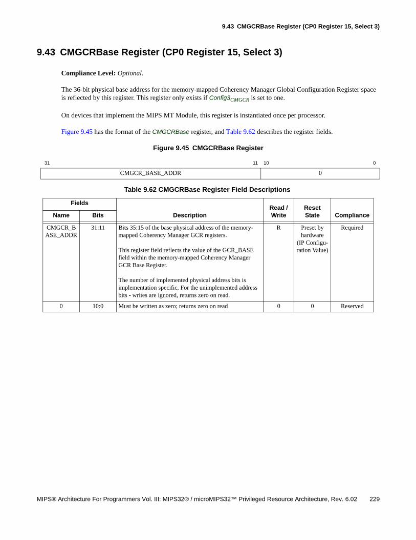
9.43 CMGCRBase Register (CP0 Register 15, Select 3)
MIPS® Architecture For Programmers Vol. III: MIPS32® / microMIPS32™ Privileged Resource Architecture, Rev. 6.02 229
9.43 CMGCRBase Register (CP0 Register 15, Select 3)
Compliance Level: Optional.
The 36-bit physical base address for the memory-mapped Coherency Manager Global Configuration Register space is reflected by this register. This register only exists if Config3CMGCR is set to one.
On devices that implement the MIPS MT Module, this register is instantiated once per processor.
Figure 9.45 has the format of the CMGCRBase register, and Table 9.62 describes the register fields.
Figure 9.45 CMGCRBase Register
31 11 10 0
CMGCR_BASE_ADDR 0
Table 9.62 CMGCRBase Register Field Descriptions
Fields
DescriptionRead / Write
Reset State ComplianceName Bits
CMGCR_BASE_ADDR
31:11 Bits 35:15 of the base physical address of the memory- mapped Coherency Manager GCR registers.
This register field reflects the value of the GCR_BASE field within the memory-mapped Coherency Manager GCR Base Register.
The number of implemented physical address bits is implementation specific. For the unimplemented address bits - writes are ignored, returns zero on read.
R Preset by hardware
(IP Configu-ration Value)
Required
0 10:0 Must be written as zero; returns zero on read 0 0 Reserved

230 MIPS® Architecture For Programmers Vol. III: MIPS32® / microMIPS32™ Privileged Resource Architecture, Rev. 6.02
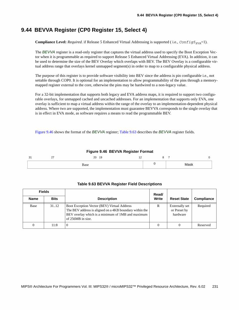
9.44 BEVVA Register (CP0 Register 15, Select 4)
MIPS® Architecture For Programmers Vol. III: MIPS32® / microMIPS32™ Privileged Resource Architecture, Rev. 6.02 231
9.44 BEVVA Register (CP0 Register 15, Select 4)
Compliance Level: Required. if Release 5 Enhanced Virtual Addressing is supported ( i.e., Config5EVA=1).
The BEVVA register is a read-only register that captures the virtual address used to specify the Boot Exception Vec-tor when it is programmable as required to support Release 5 Enhanced Virtual Addressing (EVA). In addition, it can be used to determine the size of the BEV Overlay which overlaps with BEV. The BEV Overlay is a configurable vir-tual address range that overlays kernel unmapped segment(s) in order to map to a configurable physical address.
The purpose of this register is to provide software visibility into BEV since the address is pin configurable i.e., not settable through COP0. It is optional for an implementation to allow programmability of the pins through a memory-mapped register external to the core, otherwise the pins may be hardwired to a non-legacy value.
For a 32-bit implementation that supports both legacy and EVA address maps, it is required to support two configu-rable overlays, for unmapped cached and uncached addresses. For an implementation that supports only EVA, one overlay is sufficient to map a virtual address within the range of the overlay to an implementation-dependent physical address. Where two are supported, the implementation must guarantee BEVVA corresponds to the single overlay that is in effect in EVA mode, as software requires a means to read the programmable BEV.
Figure 9.46 shows the format of the BEVVA register; Table 9.63 describes the BEVVA register fields.
Figure 9.46 BEVVA Register Format
31 27 20 19 12 8 7 0
Base 0 Mask
Table 9.63 BEVVA Register Field Descriptions
Fields
DescriptionRead/Write Reset State ComplianceName Bits
Base 31..12 Boot Exception Vector (BEV) Virtual AddressThe BEV address is aligned on a 4KB boundary within the BEV overlay which is a minimum of 1MB and maximum of 256MB in size.
R Externally set or Preset by
hardware
Required
0 11:8 0 0 0 Reserved
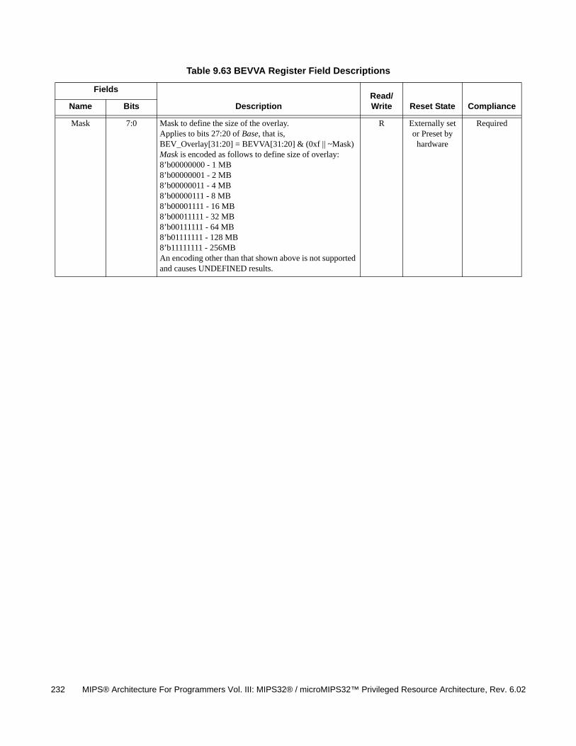
232 MIPS® Architecture For Programmers Vol. III: MIPS32® / microMIPS32™ Privileged Resource Architecture, Rev. 6.02
Mask 7:0 Mask to define the size of the overlay.Applies to bits 27:20 of Base, that is, BEV_Overlay[31:20] = BEVVA[31:20] & (0xf || ~Mask)Mask is encoded as follows to define size of overlay:8’b00000000 - 1 MB8’b00000001 - 2 MB8’b00000011 - 4 MB8’b00000111 - 8 MB8’b00001111 - 16 MB8’b00011111 - 32 MB8’b00111111 - 64 MB8’b01111111 - 128 MB8’b11111111 - 256MBAn encoding other than that shown above is not supported and causes UNDEFINED results.
R Externally set or Preset by
hardware
Required
Table 9.63 BEVVA Register Field Descriptions
Fields
DescriptionRead/Write Reset State ComplianceName Bits
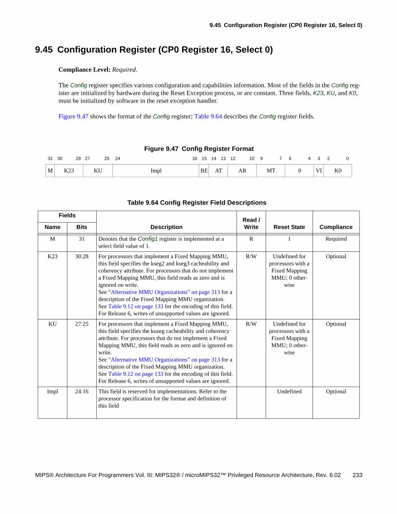
9.45 Configuration Register (CP0 Register 16, Select 0)
MIPS® Architecture For Programmers Vol. III: MIPS32® / microMIPS32™ Privileged Resource Architecture, Rev. 6.02 233
9.45 Configuration Register (CP0 Register 16, Select 0)
Compliance Level: Required.
The Config register specifies various configuration and capabilities information. Most of the fields in the Config reg-ister are initialized by hardware during the Reset Exception process, or are constant. Three fields, K23, KU, and K0, must be initialized by software in the reset exception handler.
Figure 9.47 shows the format of the Config register; Table 9.64 describes the Config register fields.
Figure 9.47 Config Register Format
31 30 28 27 25 24 16 15 14 13 12 10 9 7 6 4 3 2 0
M K23 KU Impl BE AT AR MT 0 VI K0
Table 9.64 Config Register Field Descriptions
Fields
DescriptionRead / Write Reset State ComplianceName Bits
M 31 Denotes that the Config1 register is implemented at a select field value of 1.
R 1 Required
K23 30:28 For processors that implement a Fixed Mapping MMU, this field specifies the kseg2 and kseg3 cacheability and coherency attribute. For processors that do not implement a Fixed Mapping MMU, this field reads as zero and is ignored on write.See “Alternative MMU Organizations” on page 313 for a description of the Fixed Mapping MMU organization.See Table 9.12 on page 133 for the encoding of this field. For Release 6, writes of unsupported values are ignored.
R/W Undefined for processors with a Fixed Mapping MMU; 0 other-
wise
Optional
KU 27:25 For processors that implement a Fixed Mapping MMU, this field specifies the kuseg cacheability and coherency attribute. For processors that do not implement a Fixed Mapping MMU, this field reads as zero and is ignored on write.See “Alternative MMU Organizations” on page 313 for a description of the Fixed Mapping MMU organization.See Table 9.12 on page 133 for the encoding of this field.For Release 6, writes of unsupported values are ignored.
R/W Undefined for processors with a Fixed Mapping MMU; 0 other-
wise
Optional
Impl 24:16 This field is reserved for implementations. Refer to the processor specification for the format and definition of this field
Undefined Optional
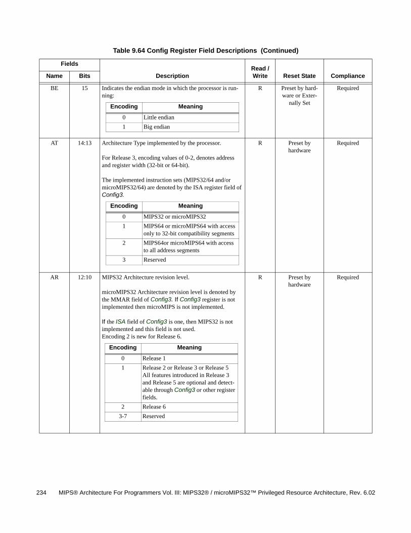
234 MIPS® Architecture For Programmers Vol. III: MIPS32® / microMIPS32™ Privileged Resource Architecture, Rev. 6.02
BE 15 Indicates the endian mode in which the processor is run-ning:
R Preset by hard-ware or Exter-
nally Set
Required
AT 14:13 Architecture Type implemented by the processor.
For Release 3, encoding values of 0-2, denotes address and register width (32-bit or 64-bit).
The implemented instruction sets (MIPS32/64 and/or microMIPS32/64) are denoted by the ISA register field of Config3.
R Preset by hardware
Required
AR 12:10 MIPS32 Architecture revision level.
microMIPS32 Architecture revision level is denoted by the MMAR field of Config3. If Config3 register is not implemented then microMIPS is not implemented.
If the ISA field of Config3 is one, then MIPS32 is not implemented and this field is not used.Encoding 2 is new for Release 6.
R Preset by hardware
Required
Table 9.64 Config Register Field Descriptions (Continued)
Fields
DescriptionRead / Write Reset State ComplianceName Bits
Encoding Meaning
0 Little endian
1 Big endian
Encoding Meaning
0 MIPS32 or microMIPS32
1 MIPS64 or microMIPS64 with access only to 32-bit compatibility segments
2 MIPS64or microMIPS64 with access to all address segments
3 Reserved
Encoding Meaning
0 Release 1
1 Release 2 or Release 3 or Release 5All features introduced in Release 3 and Release 5 are optional and detect-able through Config3 or other register fields.
2 Release 6
3-7 Reserved
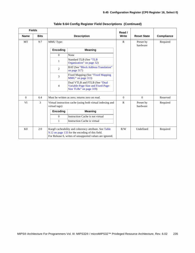
9.45 Configuration Register (CP0 Register 16, Select 0)
MIPS® Architecture For Programmers Vol. III: MIPS32® / microMIPS32™ Privileged Resource Architecture, Rev. 6.02 235
MT 9:7 MMU Type: R Preset by hardware
Required
0 6:4 Must be written as zero; returns zero on read. 0 0 Reserved
VI 3 Virtual instruction cache (using both virtual indexing and virtual tags):
R Preset by hardware
Required
K0 2:0 Kseg0 cacheability and coherency attribute. See Table 9.12 on page 133 for the encoding of this field.For Release 6, writes of unsupported values are ignored.
R/W Undefined Required
Table 9.64 Config Register Field Descriptions (Continued)
Fields
DescriptionRead / Write Reset State ComplianceName Bits
Encoding Meaning
0 None
1 Standard TLB (See “TLB Organization” on page 32)
2 BAT (See “Block Address Translation” on page 317)
3 Fixed Mapping (See “Fixed Mapping MMU” on page 313)
4Dual VTLB and FTLB (See “Dual Variable-Page-Size and Fixed-Page-Size TLBs” on page 319)
Encoding Meaning
0 Instruction Cache is not virtual
1 Instruction Cache is virtual

236 MIPS® Architecture For Programmers Vol. III: MIPS32® / microMIPS32™ Privileged Resource Architecture, Rev. 6.02
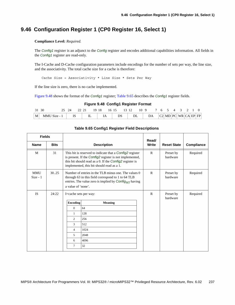
9.46 Configuration Register 1 (CP0 Register 16, Select 1)
MIPS® Architecture For Programmers Vol. III: MIPS32® / microMIPS32™ Privileged Resource Architecture, Rev. 6.02 237
9.46 Configuration Register 1 (CP0 Register 16, Select 1)
Compliance Level: Required.
The Config1 register is an adjunct to the Config register and encodes additional capabilities information. All fields in the Config1 register are read-only.
The I-Cache and D-Cache configuration parameters include encodings for the number of sets per way, the line size, and the associativity. The total cache size for a cache is therefore:
Cache Size = Associativity * Line Size * Sets Per Way
If the line size is zero, there is no cache implemented.
Figure 9.48 shows the format of the Config1 register; Table 9.65 describes the Config1 register fields.
Figure 9.48 Config1 Register Format
31 30 25 24 22 21 19 18 16 15 13 12 10 9 7 6 5 4 3 2 1 0
M MMU Size - 1 IS IL IA DS DL DA C2 MD PC WR CA EP FP
Table 9.65 Config1 Register Field Descriptions
Fields
DescriptionRead/Write Reset State ComplianceName Bits
M 31 This bit is reserved to indicate that a Config2 register is present. If the Config2 register is not implemented, this bit should read as a 0. If the Config2 register is implemented, this bit should read as a 1.
R Preset by hardware
Required
MMU Size - 1
30..25 Number of entries in the TLB minus one. The values 0 through 63 in this field correspond to 1 to 64 TLB entries. The value zero is implied by ConfigMT having
a value of ‘none’.
R Preset by hardware
Required
IS 24:22 I=cache sets per way:
R Preset by hardware
Required
Encoding Meaning
0 64
1 128
2 256
3 512
4 1024
5 2048
6 4096
7 32
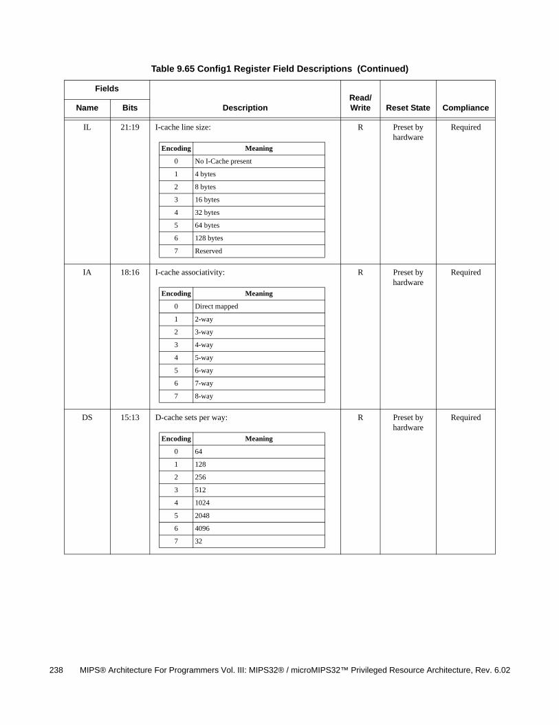
238 MIPS® Architecture For Programmers Vol. III: MIPS32® / microMIPS32™ Privileged Resource Architecture, Rev. 6.02
IL 21:19 I-cache line size:
R Preset by hardware
Required
IA 18:16 I-cache associativity:
R Preset by hardware
Required
DS 15:13 D-cache sets per way:
R Preset by hardware
Required
Table 9.65 Config1 Register Field Descriptions (Continued)
Fields
DescriptionRead/Write Reset State ComplianceName Bits
Encoding Meaning
0 No I-Cache present
1 4 bytes
2 8 bytes
3 16 bytes
4 32 bytes
5 64 bytes
6 128 bytes
7 Reserved
Encoding Meaning
0 Direct mapped
1 2-way
2 3-way
3 4-way
4 5-way
5 6-way
6 7-way
7 8-way
Encoding Meaning
0 64
1 128
2 256
3 512
4 1024
5 2048
6 4096
7 32
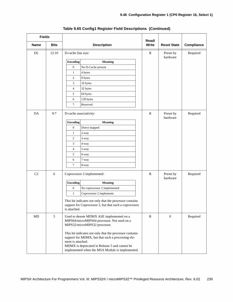
9.46 Configuration Register 1 (CP0 Register 16, Select 1)
MIPS® Architecture For Programmers Vol. III: MIPS32® / microMIPS32™ Privileged Resource Architecture, Rev. 6.02 239
DL 12:10 D-cache line size:
R Preset by hardware
Required
DA 9:7 D-cache associativity:
R Preset by hardware
Required
C2 6 Coprocessor 2 implemented:
This bit indicates not only that the processor contains support for Coprocessor 2, but that such a coprocessor is attached.
R Preset by hardware
Required
MD 5 Used to denote MDMX ASE implemented on a MIPS64/microMIPS64 processor. Not used on a MIPS32/microMIPS32 processor.
This bit indicates not only that the processor contains support for MDMX, but that such a processing ele-ment is attached.MDMX is deprecated in Release 5 and cannot be implemented when the MSA Module is implemented.
R 0 Required
Table 9.65 Config1 Register Field Descriptions (Continued)
Fields
DescriptionRead/Write Reset State ComplianceName Bits
Encoding Meaning
0 No D-Cache present
1 4 bytes
2 8 bytes
3 16 bytes
4 32 bytes
5 64 bytes
6 128 bytes
7 Reserved
Encoding Meaning
0 Direct mapped
1 2-way
2 3-way
3 4-way
4 5-way
5 6-way
6 7-way
7 8-way
Encoding Meaning
0 No coprocessor 2 implemented
1 Coprocessor 2 implements
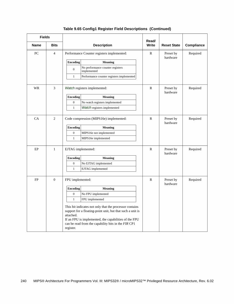
240 MIPS® Architecture For Programmers Vol. III: MIPS32® / microMIPS32™ Privileged Resource Architecture, Rev. 6.02
PC 4 Performance Counter registers implemented:
R Preset by hardware
Required
WR 3 Watch registers implemented:
R Preset by hardware
Required
CA 2 Code compression (MIPS16e) implemented:
R Preset by hardware
Required
EP 1 EJTAG implemented:
R Preset by hardware
Required
FP 0 FPU implemented:
This bit indicates not only that the processor contains support for a floating-point unit, but that such a unit is attached.If an FPU is implemented, the capabilities of the FPU can be read from the capability bits in the FIR CP1 register.
R Preset by hardware
Required
Table 9.65 Config1 Register Field Descriptions (Continued)
Fields
DescriptionRead/Write Reset State ComplianceName Bits
Encoding Meaning
0No performance counter registers implemented
1 Performance counter registers implemented
Encoding Meaning
0 No watch registers implemented
1 Watch registers implemented
Encoding Meaning
0 MIPS16e not implemented
1 MIPS16e implemented
Encoding Meaning
0 No EJTAG implemented
1 EJTAG implemented
Encoding Meaning
0 No FPU implemented
1 FPU implemented
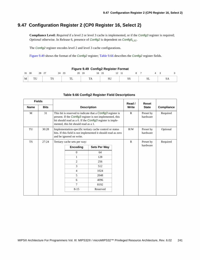
9.47 Configuration Register 2 (CP0 Register 16, Select 2)
MIPS® Architecture For Programmers Vol. III: MIPS32® / microMIPS32™ Privileged Resource Architecture, Rev. 6.02 241
9.47 Configuration Register 2 (CP0 Register 16, Select 2)
Compliance Level: Required if a level 2 or level 3 cache is implemented, or if the Config3 register is required; Optional otherwise. In Release 6, presence of Config2 is dependent on Config5L2C.
The Config2 register encodes level 2 and level 3 cache configurations.
Figure 9.49 shows the format of the Config2 register; Table 9.66 describes the Config2 register fields.
Figure 9.49 Config2 Register Format31 30 28 27 24 23 20 19 16 15 12 11 8 7 4 3 0
M TU TS TL TA SU SS SL SA
Table 9.66 Config2 Register Field Descriptions
Fields
DescriptionRead / Write
Reset State ComplianceName Bits
M 31 This bit is reserved to indicate that a Config3 register is present. If the Config3 register is not implemented, this bit should read as a 0. If the Config3 register is imple-mented, this bit should read as a 1.
R Preset by hardware
Required
TU 30:28 Implementation-specific tertiary cache control or status bits. If this field is not implemented it should read as zero and be ignored on write.
R/W Preset by hardware
Optional
TS 27:24 Tertiary cache sets per way: R Preset by hardware
Required
Encoding Sets Per Way
0 64
1 128
2 256
3 512
4 1024
5 2048
6 4096
7 8192
8-15 Reserved
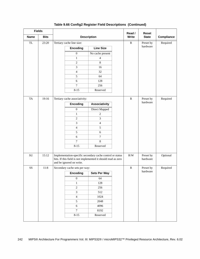
242 MIPS® Architecture For Programmers Vol. III: MIPS32® / microMIPS32™ Privileged Resource Architecture, Rev. 6.02
TL 23:20 Tertiary cache line size: R Preset by hardware
Required
TA 19:16 Tertiary cache associativity: R Preset by hardware
Required
SU 15:12 Implementation-specific secondary cache control or status bits. If this field is not implemented it should read as zero and be ignored on write.
R/W Preset by hardware
Optional
SS 11:8 Secondary cache sets per way: R Preset by hardware
Required
Table 9.66 Config2 Register Field Descriptions (Continued)
Fields
DescriptionRead / Write
Reset State ComplianceName Bits
Encoding Line Size
0 No cache present
1 4
2 8
3 16
4 32
5 64
6 128
7 256
8-15 Reserved
Encoding Associativity
0 Direct Mapped
1 2
2 3
3 4
4 5
5 6
6 7
7 8
8-15 Reserved
Encoding Sets Per Way
0 64
1 128
2 256
3 512
4 1024
5 2048
6 4096
7 8192
8-15 Reserved
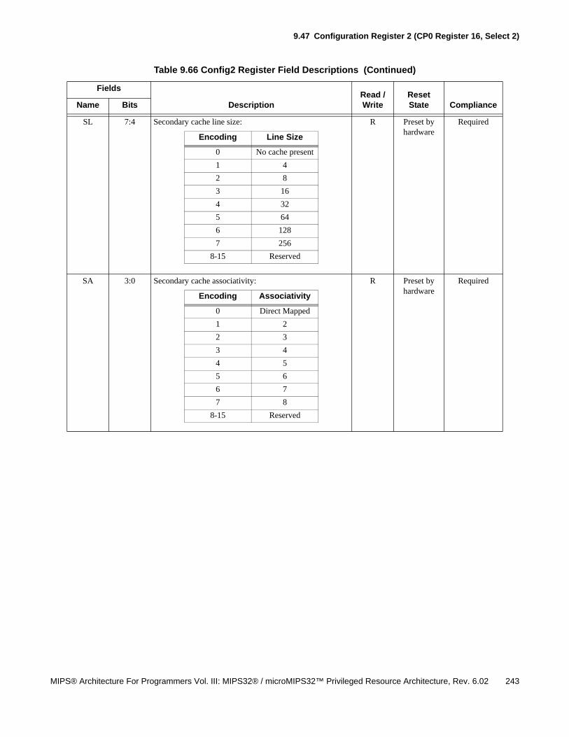
9.47 Configuration Register 2 (CP0 Register 16, Select 2)
MIPS® Architecture For Programmers Vol. III: MIPS32® / microMIPS32™ Privileged Resource Architecture, Rev. 6.02 243
SL 7:4 Secondary cache line size: R Preset by hardware
Required
SA 3:0 Secondary cache associativity: R Preset by hardware
Required
Table 9.66 Config2 Register Field Descriptions (Continued)
Fields
DescriptionRead / Write
Reset State ComplianceName Bits
Encoding Line Size
0 No cache present
1 4
2 8
3 16
4 32
5 64
6 128
7 256
8-15 Reserved
Encoding Associativity
0 Direct Mapped
1 2
2 3
3 4
4 5
5 6
6 7
7 8
8-15 Reserved

244 MIPS® Architecture For Programmers Vol. III: MIPS32® / microMIPS32™ Privileged Resource Architecture, Rev. 6.02
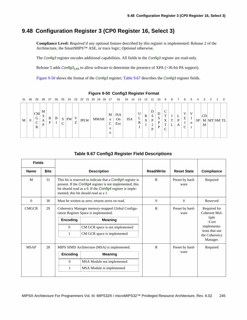
9.48 Configuration Register 3 (CP0 Register 16, Select 3)
MIPS® Architecture For Programmers Vol. III: MIPS32® / microMIPS32™ Privileged Resource Architecture, Rev. 6.02 245
9.48 Configuration Register 3 (CP0 Register 16, Select 3)
Compliance Level: Required if any optional feature described by this register is implemented: Release 2 of the Architecture, the SmartMIPS™ ASE, or trace logic; Optional otherwise.
The Config3 register encodes additional capabilities. All fields in the Config3 register are read-only.
Release 5 adds Config3LPA to allow software to determine the presence of XPA (>36-bit PA support).
Figure 9-50 shows the format of the Config3 register; Table 9.67 describes the Config3 register fields.
Figure 9-50 Config3 Register Format
31 30 29 28 27 26 25 24 23 22 21 20 19 18 17 16 15 14 13 12 11 10 9 8 7 6 5 4 3 2 1 0
M 0
CMGCR
MSAP
BP
BI
SC
PW VZ
IPLW MMARMuCon
ISAOnExc
ISA
ULRI
RXI
DSP2P
DSPP
CTXTC
ITL
LPA
VEIC
VInt
SPCDMM
MT SM TL
Table 9.67 Config3 Register Field Descriptions
Fields
Description Read/Write Reset State ComplianceName Bits
M 31 This bit is reserved to indicate that a Config4 register is present. If the Config4 register is not implemented, this bit should read as a 0. If the Config4 register is imple-mented, this bit should read as a 1.
R Preset by hard-ware
Required
0 30 Must be written as zero; returns zeros on read. 0 0 Reserved
CMGCR 29 Coherency Manager memory-mapped Global Configu-ration Register Space is implemented.
R Preset by hard-ware
Required for Coherent Mul-
tiple-Core
implementa-tions that use
the Coherency Manager.
MSAP 28 MIPS SIMD Architecture (MSA) is implemented. R Preset by hard-ware
Required
Encoding Meaning
0 CM GCR space is not implemented
1 CM GCR space is implemented
Encoding Meaning
0 MSA Module not implemented
1 MSA Module is implemented
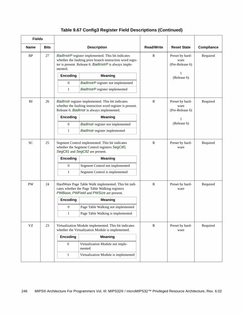
246 MIPS® Architecture For Programmers Vol. III: MIPS32® / microMIPS32™ Privileged Resource Architecture, Rev. 6.02
BP 27 BadInstrP register implemented. This bit indicates whether the faulting prior branch instruction word regis-ter is present. Release 6: BadInstrP is always imple-mented.
R Preset by hard-ware
(Pre-Release 6)
1(Release 6)
Required
BI 26 BadInstr register implemented. This bit indicates whether the faulting instruction word register is present. Release 6: BadInstr is always implemented.
R Preset by hard-ware
(Pre-Release 6)
1(Release 6)
Required
SC 25 Segment Control implemented. This bit indicates whether the Segment Control registers SegCtl0, SegCtl1 and SegCtl2 are present.
R Preset by hard-ware
Required
PW 24 HardWare Page Table Walk implemented. This bit indi-cates whether the Page Table Walking registers PWBase, PWField and PWSize are present.
R Preset by hard-ware
Required
VZ 23 Virtualization Module implemented. This bit indicates whether the Virtualization Module is implemented.
R Preset by hard-ware
Required
Table 9.67 Config3 Register Field Descriptions (Continued)
Fields
Description Read/Write Reset State ComplianceName Bits
Encoding Meaning
0 BadInstrP register not implemented
1 BadInstrP register implemented
Encoding Meaning
0 BadInstr register not implemented
1 BadInstr register implemented
Encoding Meaning
0 Segment Control not implemented
1 Segment Control is implemented
Encoding Meaning
0 Page Table Walking not implemented
1 Page Table Walking is implemented
Encoding Meaning
0 Virtualization Module not imple-mented
1 Virtualization Module is implemented
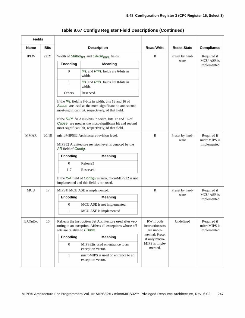
9.48 Configuration Register 3 (CP0 Register 16, Select 3)
MIPS® Architecture For Programmers Vol. III: MIPS32® / microMIPS32™ Privileged Resource Architecture, Rev. 6.02 247
IPLW 22:21 Width of StatusIPL and CauseRIPL fields:
If the IPL field is 8-bits in width, bits 18 and 16 of Status are used as the most-significant bit and second most-significant bit, respectively, of that field.
If the RIPL field is 8-bits in width, bits 17 and 16 of Cause are used as the most-significant bit and second most-significant bit, respectively, of that field.
R Preset by hard-ware
Required if MCU ASE is implemented
MMAR 20:18 microMIPS32 Architecture revision level.
MIPS32 Architecture revision level is denoted by the AR field of Config.
If the ISA field of Config3 is zero, microMIPS32 is not implemented and this field is not used.
R Preset by hard-ware
Required if microMIPS is implemented
MCU 17 MIPS® MCU ASE is implemented. R Preset by hard-ware
Required if MCU ASE is implemented
ISAOnExc 16 Reflects the Instruction Set Architecture used after vec-toring to an exception. Affects all exceptions whose off-sets are relative to EBase.
RW if both instruction sets
are imple-mented; Preset if only micro-
MIPS is imple-mented.
Undefined Required if microMIPS is implemented
Table 9.67 Config3 Register Field Descriptions (Continued)
Fields
Description Read/Write Reset State ComplianceName Bits
Encoding Meaning
0 IPL and RIPL fields are 6-bits in width.
1 IPL and RIPL fields are 8-bits in width.
Others Reserved.
Encoding Meaning
0 Release3
1-7 Reserved
Encoding Meaning
0 MCU ASE is not implemented.
1 MCU ASE is implemented
Encoding Meaning
0 MIPS32is used on entrance to an exception vector.
1 microMIPS is used on entrance to an exception vector.
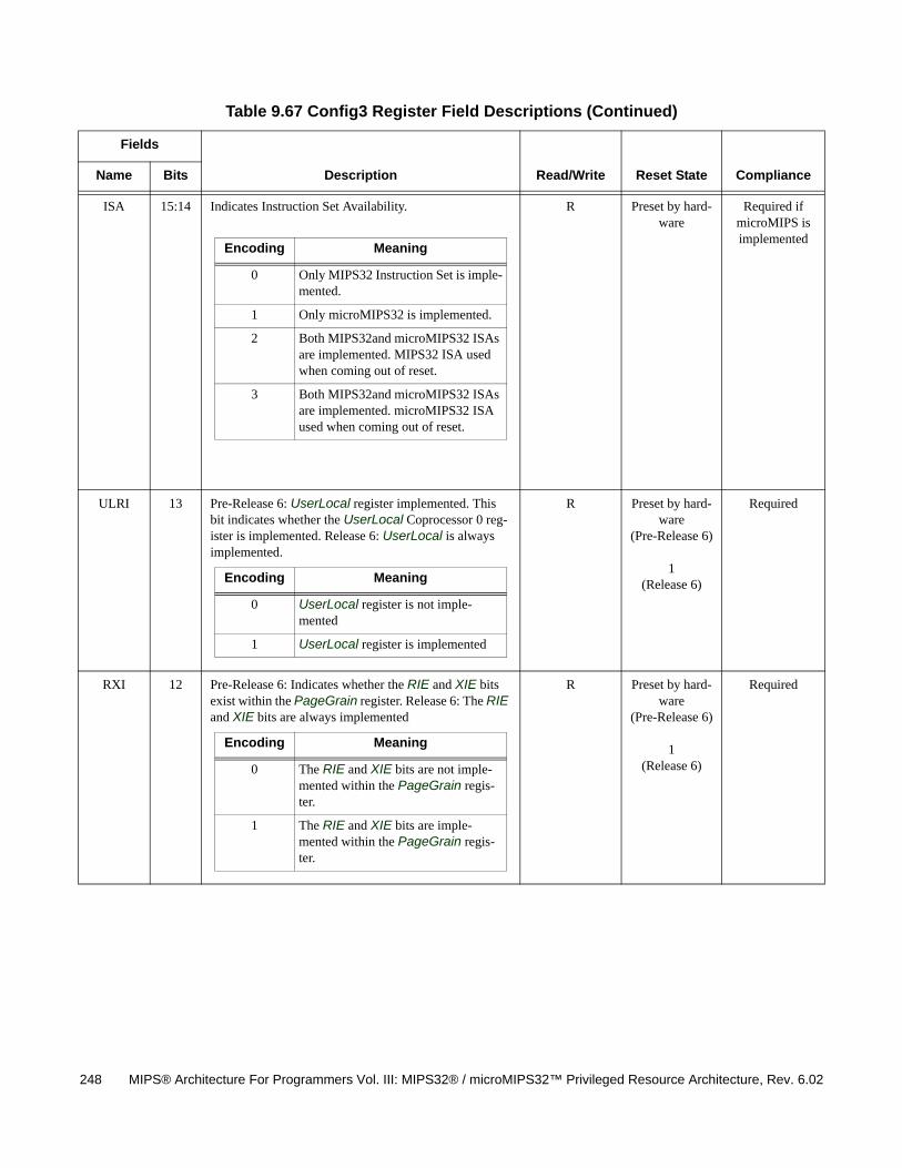
248 MIPS® Architecture For Programmers Vol. III: MIPS32® / microMIPS32™ Privileged Resource Architecture, Rev. 6.02
ISA 15:14 Indicates Instruction Set Availability. R Preset by hard-ware
Required if microMIPS is implemented
ULRI 13 Pre-Release 6: UserLocal register implemented. This bit indicates whether the UserLocal Coprocessor 0 reg-ister is implemented. Release 6: UserLocal is always implemented.
R Preset by hard-ware
(Pre-Release 6)
1(Release 6)
Required
RXI 12 Pre-Release 6: Indicates whether the RIE and XIE bits exist within the PageGrain register. Release 6: The RIE and XIE bits are always implemented
R Preset by hard-ware
(Pre-Release 6)
1(Release 6)
Required
Table 9.67 Config3 Register Field Descriptions (Continued)
Fields
Description Read/Write Reset State ComplianceName Bits
Encoding Meaning
0 Only MIPS32 Instruction Set is imple-mented.
1 Only microMIPS32 is implemented.
2 Both MIPS32and microMIPS32 ISAs are implemented. MIPS32 ISA used when coming out of reset.
3 Both MIPS32and microMIPS32 ISAs are implemented. microMIPS32 ISA used when coming out of reset.
Encoding Meaning
0 UserLocal register is not imple-mented
1 UserLocal register is implemented
Encoding Meaning
0 The RIE and XIE bits are not imple-mented within the PageGrain regis-ter.
1 The RIE and XIE bits are imple-mented within the PageGrain regis-ter.
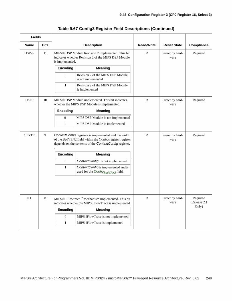
9.48 Configuration Register 3 (CP0 Register 16, Select 3)
MIPS® Architecture For Programmers Vol. III: MIPS32® / microMIPS32™ Privileged Resource Architecture, Rev. 6.02 249
DSP2P 11 MIPS® DSP Module Revision 2 implemented. This bit indicates whether Revision 2 of the MIPS DSP Module is implemented.
R Preset by hard-ware
Required
DSPP 10 MIPS® DSP Module implemented. This bit indicates whether the MIPS DSP Module is implemented.
R Preset by hard-ware
Required
CTXTC 9 ContextConfig registers is implemented and the width of the BadVPN2 field within the Config register register depends on the contents of the ContextConfig register. .
R Preset by hard-ware
Required
ITL 8 MIPS® IFlowtrace™ mechanism implemented. This bit indicates whether the MIPS IFlowTrace is implemented.
R Preset by hard-ware
Required(Release 2.1
Only)
Table 9.67 Config3 Register Field Descriptions (Continued)
Fields
Description Read/Write Reset State ComplianceName Bits
Encoding Meaning
0 Revision 2 of the MIPS DSP Module is not implemented
1 Revision 2 of the MIPS DSP Module is implemented
Encoding Meaning
0 MIPS DSP Module is not implemented
1 MIPS DSP Module is implemented
Encoding Meaning
0 ContextConfig is not implemented.
1 ContextConfig is implemented and is used for the ConfigBadVPN2 field.
Encoding Meaning
0 MIPS IFlowTrace is not implemented
1 MIPS IFlowTrace is implemented
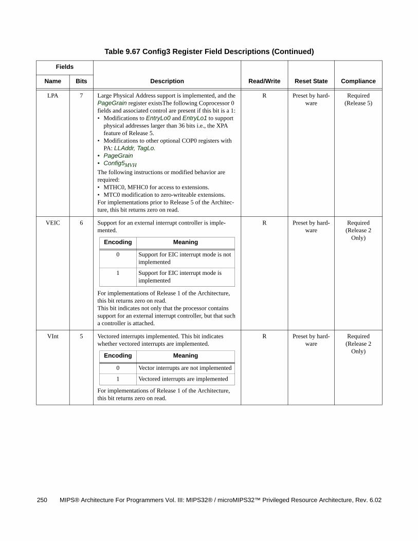
250 MIPS® Architecture For Programmers Vol. III: MIPS32® / microMIPS32™ Privileged Resource Architecture, Rev. 6.02
LPA 7 Large Physical Address support is implemented, and the PageGrain register existsThe following Coprocessor 0 fields and associated control are present if this bit is a 1:• Modifications to EntryLo0 and EntryLo1 to support
physical addresses larger than 36 bits i.e., the XPA feature of Release 5.
• Modifications to other optional COP0 registers with PA: LLAddr, TagLo.
• PageGrain• Config5MVHThe following instructions or modified behavior are required:• MTHC0, MFHC0 for access to extensions.• MTC0 modification to zero-writeable extensions.For implementations prior to Release 5 of the Architec-ture, this bit returns zero on read.
R Preset by hard-ware
Required (Release 5)
VEIC 6 Support for an external interrupt controller is imple-mented.
For implementations of Release 1 of the Architecture, this bit returns zero on read.This bit indicates not only that the processor contains support for an external interrupt controller, but that such a controller is attached.
R Preset by hard-ware
Required (Release 2
Only)
VInt 5 Vectored interrupts implemented. This bit indicates whether vectored interrupts are implemented.
For implementations of Release 1 of the Architecture, this bit returns zero on read.
R Preset by hard-ware
Required (Release 2
Only)
Table 9.67 Config3 Register Field Descriptions (Continued)
Fields
Description Read/Write Reset State ComplianceName Bits
Encoding Meaning
0 Support for EIC interrupt mode is not implemented
1 Support for EIC interrupt mode is implemented
Encoding Meaning
0 Vector interrupts are not implemented
1 Vectored interrupts are implemented
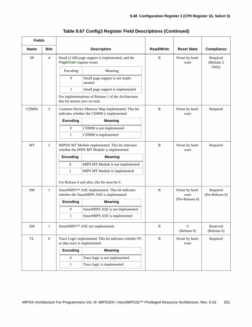
9.48 Configuration Register 3 (CP0 Register 16, Select 3)
MIPS® Architecture For Programmers Vol. III: MIPS32® / microMIPS32™ Privileged Resource Architecture, Rev. 6.02 251
SP 4 Small (1 kB) page support is implemented, and the PageGrain register exists
For implementations of Release 1 of the Architecture, this bit returns zero on read.
R Preset by hard-ware
Required (Release 2
Only)
CDMM 3 Common Device Memory Map implemented. This bit indicates whether the CDMM is implemented.
R Preset by hard-ware
Required
MT 2 MIPS® MT Module implemented. This bit indicates whether the MIPS MT Module is implemented.
For Release 6 and after, this bit must be 0.
R Preset by hard-ware
Required
SM 1 SmartMIPS™ ASE implemented. This bit indicates whether the SmartMIPS ASE is implemented.
R Preset by hard-ware
(Pre-Release 6)
Required(Pre-Release 6)
SM 1 SmartMIPS™ ASE not implemented. R 0(Release 6)
Reserved(Release 6)
TL 0 Trace Logic implemented. This bit indicates whether PC or data trace is implemented.
R Preset by hard-ware
Required
Table 9.67 Config3 Register Field Descriptions (Continued)
Fields
Description Read/Write Reset State ComplianceName Bits
Encoding Meaning
0 Small page support is not imple-mented
1 Small page support is implemented
Encoding Meaning
0 CDMM is not implemented
1 CDMM is implemented
Encoding Meaning
0 MIPS MT Module is not implemented
1 MIPS MT Module is implemented
Encoding Meaning
0 SmartMIPS ASE is not implemented
1 SmartMIPS ASE is implemented
Encoding Meaning
0 Trace logic is not implemented
1 Trace logic is implemented

252 MIPS® Architecture For Programmers Vol. III: MIPS32® / microMIPS32™ Privileged Resource Architecture, Rev. 6.02
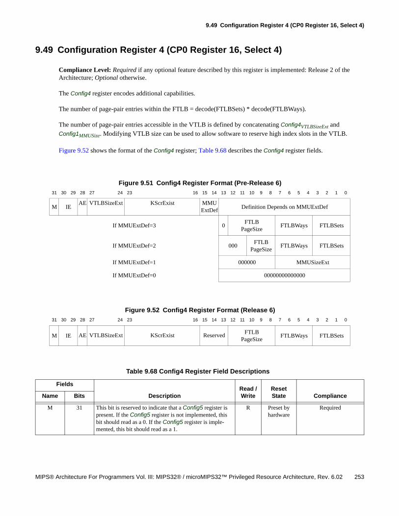
9.49 Configuration Register 4 (CP0 Register 16, Select 4)
MIPS® Architecture For Programmers Vol. III: MIPS32® / microMIPS32™ Privileged Resource Architecture, Rev. 6.02 253
9.49 Configuration Register 4 (CP0 Register 16, Select 4)
Compliance Level: Required if any optional feature described by this register is implemented: Release 2 of the Architecture; Optional otherwise.
The Config4 register encodes additional capabilities.
The number of page-pair entries within the FTLB = decode(FTLBSets) * decode(FTLBWays).
The number of page-pair entries accessible in the VTLB is defined by concatenating Config4VTLBSizeExt and
Config1MMUSize. Modifying VTLB size can be used to allow software to reserve high index slots in the VTLB.
Figure 9.52 shows the format of the Config4 register; Table 9.68 describes the Config4 register fields.
Figure 9.51 Config4 Register Format (Pre-Release 6)
31 30 29 28 27 24 23 16 15 14 13 12 11 10 9 8 7 6 5 4 3 2 1 0
M IEAE VTLBSizeExt KScrExist MMU
ExtDefDefinition Depends on MMUExtDef
If MMUExtDef=3 0FTLB
PageSizeFTLBWays FTLBSets
If MMUExtDef=2 000FTLB
PageSizeFTLBWays FTLBSets
If MMUExtDef=1 000000 MMUSizeExt
If MMUExtDef=0 00000000000000
Figure 9.52 Config4 Register Format (Release 6)
31 30 29 28 27 24 23 16 15 14 13 12 11 10 9 8 7 6 5 4 3 2 1 0
M IE AE VTLBSizeExt KScrExist Reserved FTLBPageSize
FTLBWays FTLBSets
Table 9.68 Config4 Register Field Descriptions
Fields
DescriptionRead / Write
Reset State ComplianceName Bits
M 31 This bit is reserved to indicate that a Config5 register is present. If the Config5 register is not implemented, this bit should read as a 0. If the Config5 register is imple-mented, this bit should read as a 1.
R Preset by hardware
Required
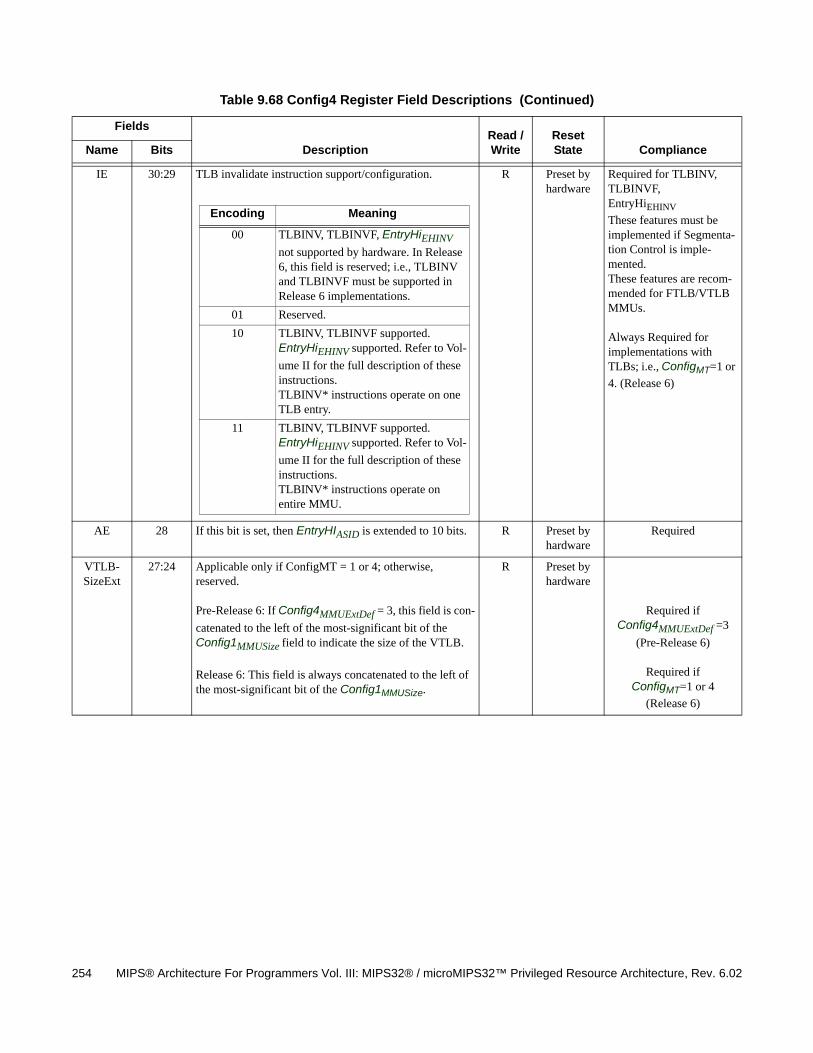
254 MIPS® Architecture For Programmers Vol. III: MIPS32® / microMIPS32™ Privileged Resource Architecture, Rev. 6.02
IE 30:29 TLB invalidate instruction support/configuration.
R Preset by hardware
Required for TLBINV, TLBINVF,EntryHiEHINV
These features must be implemented if Segmenta-tion Control is imple-mented.These features are recom-mended for FTLB/VTLB MMUs.
Always Required for implementations with TLBs; i.e., ConfigMT=1 or
4. (Release 6)
AE 28 If this bit is set, then EntryHIASID is extended to 10 bits. R Preset by hardware
Required
VTLB-SizeExt
27:24 Applicable only if ConfigMT = 1 or 4; otherwise, reserved.
Pre-Release 6: If Config4MMUExtDef = 3, this field is con-
catenated to the left of the most-significant bit of the Config1MMUSize field to indicate the size of the VTLB.
Release 6: This field is always concatenated to the left of the most-significant bit of the Config1MMUSize.
R Preset by hardware
Required if Config4MMUExtDef =3
(Pre-Release 6)
Required ifConfigMT=1 or 4
(Release 6)
Table 9.68 Config4 Register Field Descriptions (Continued)
Fields
DescriptionRead / Write
Reset State ComplianceName Bits
Encoding Meaning
00 TLBINV, TLBINVF, EntryHiEHINV
not supported by hardware. In Release 6, this field is reserved; i.e., TLBINV and TLBINVF must be supported in Release 6 implementations.
01 Reserved.
10 TLBINV, TLBINVF supported. EntryHiEHINV supported. Refer to Vol-
ume II for the full description of these instructions. TLBINV* instructions operate on one TLB entry.
11 TLBINV, TLBINVF supported. EntryHiEHINV supported. Refer to Vol-
ume II for the full description of these instructions. TLBINV* instructions operate on entire MMU.
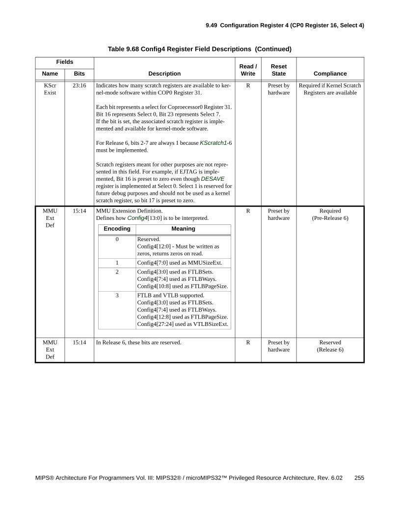
9.49 Configuration Register 4 (CP0 Register 16, Select 4)
MIPS® Architecture For Programmers Vol. III: MIPS32® / microMIPS32™ Privileged Resource Architecture, Rev. 6.02 255
KScrExist
23:16 Indicates how many scratch registers are available to ker-nel-mode software within COP0 Register 31.
Each bit represents a select for Coproecessor0 Register 31. Bit 16 represents Select 0, Bit 23 represents Select 7. If the bit is set, the associated scratch register is imple-mented and available for kernel-mode software.
For Release 6, bits 2-7 are always 1 because KScratch1-6 must be implemented.
Scratch registers meant for other purposes are not repre-sented in this field. For example, if EJTAG is imple-mented, Bit 16 is preset to zero even though DESAVE register is implemented at Select 0. Select 1 is reserved for future debug purposes and should not be used as a kernel scratch register, so bit 17 is preset to zero.
R Preset by hardware
Required if Kernel Scratch Registers are available
MMUExtDef
15:14 MMU Extension Definition.Defines how Config4[13:0] is to be interpreted.
R Preset by hardware
Required(Pre-Release 6)
MMUExtDef
15:14 In Release 6, these bits are reserved. R Preset by hardware
Reserved(Release 6)
Table 9.68 Config4 Register Field Descriptions (Continued)
Fields
DescriptionRead / Write
Reset State ComplianceName Bits
Encoding Meaning
0 Reserved. Config4[12:0] - Must be written as zeros, returns zeros on read.
1 Config4[7:0] used as MMUSizeExt.
2 Config4[3:0] used as FTLBSets.Config4[7:4] used as FTLBWays. Config4[10:8] used as FTLBPageSize.
3 FTLB and VTLB supported.Config4[3:0] used as FTLBSets.Config4[7:4] used as FTLBWays. Config4[12:8] used as FTLBPageSize.Config4[27:24] used as VTLBSizeExt.
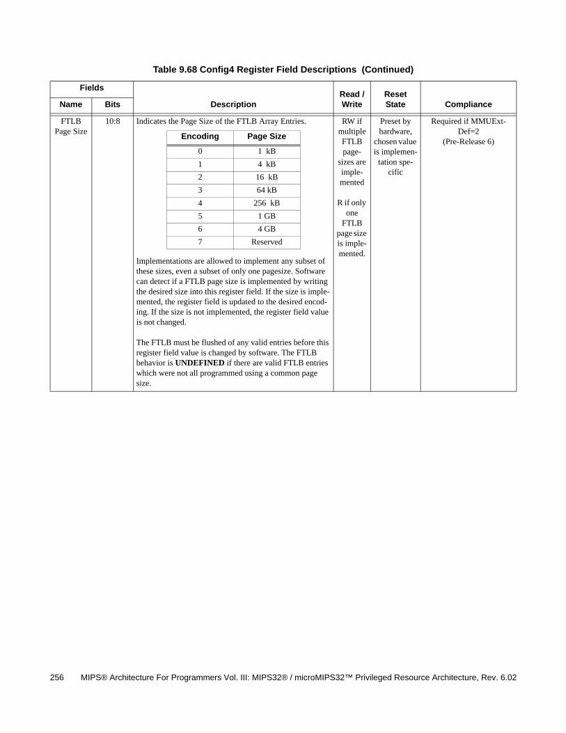
256 MIPS® Architecture For Programmers Vol. III: MIPS32® / microMIPS32™ Privileged Resource Architecture, Rev. 6.02
FTLBPage Size
10:8 Indicates the Page Size of the FTLB Array Entries.
Implementations are allowed to implement any subset of these sizes, even a subset of only one pagesize. Software can detect if a FTLB page size is implemented by writing the desired size into this register field. If the size is imple-mented, the register field is updated to the desired encod-ing. If the size is not implemented, the register field value is not changed.
The FTLB must be flushed of any valid entries before this register field value is changed by software. The FTLB behavior is UNDEFINED if there are valid FTLB entries which were not all programmed using a common page size.
RW if multiple FTLB page-
sizes are imple-mented
R if only one
FTLB page size is imple-mented.
Preset by hardware,
chosen value is implemen-
tation spe-cific
Required if MMUExt-Def=2
(Pre-Release 6)
Table 9.68 Config4 Register Field Descriptions (Continued)
Fields
DescriptionRead / Write
Reset State ComplianceName Bits
Encoding Page Size
0 1 kB
1 4 kB
2 16 kB
3 64 kB
4 256 kB
5 1 GB
6 4 GB
7 Reserved
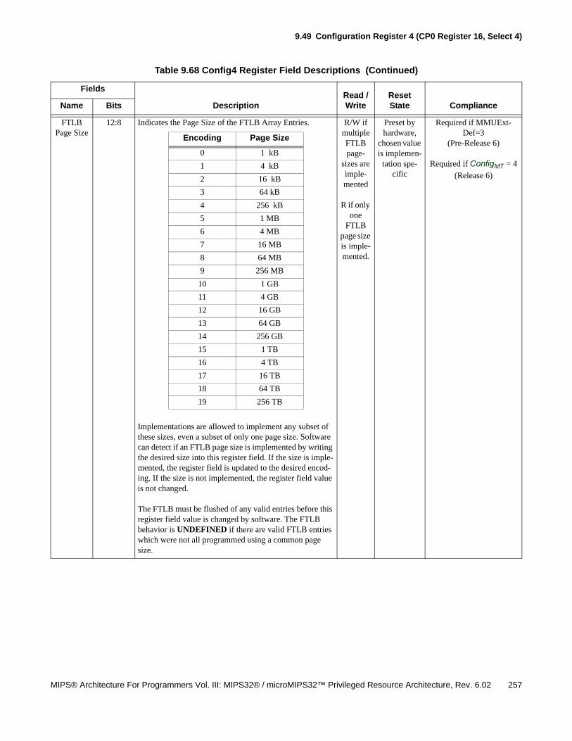
9.49 Configuration Register 4 (CP0 Register 16, Select 4)
MIPS® Architecture For Programmers Vol. III: MIPS32® / microMIPS32™ Privileged Resource Architecture, Rev. 6.02 257
FTLBPage Size
12:8 Indicates the Page Size of the FTLB Array Entries.
Implementations are allowed to implement any subset of these sizes, even a subset of only one page size. Software can detect if an FTLB page size is implemented by writing the desired size into this register field. If the size is imple-mented, the register field is updated to the desired encod-ing. If the size is not implemented, the register field value is not changed.
The FTLB must be flushed of any valid entries before this register field value is changed by software. The FTLB behavior is UNDEFINED if there are valid FTLB entries which were not all programmed using a common page size.
R/W if multiple FTLB page-
sizes are imple-mented
R if only one
FTLB page size is imple-mented.
Preset by hardware,
chosen value is implemen-
tation spe-cific
Required if MMUExt-Def=3
(Pre-Release 6)
Required if ConfigMT = 4
(Release 6)
Table 9.68 Config4 Register Field Descriptions (Continued)
Fields
DescriptionRead / Write
Reset State ComplianceName Bits
Encoding Page Size
0 1 kB
1 4 kB
2 16 kB
3 64 kB
4 256 kB
5 1 MB
6 4 MB
7 16 MB
8 64 MB
9 256 MB
10 1 GB
11 4 GB
12 16 GB
13 64 GB
14 256 GB
15 1 TB
16 4 TB
17 16 TB
18 64 TB
19 256 TB
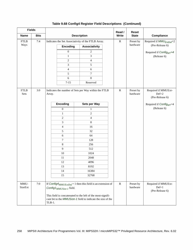
258 MIPS® Architecture For Programmers Vol. III: MIPS32® / microMIPS32™ Privileged Resource Architecture, Rev. 6.02
FTLBWays
7:4 Indicates the Set Associativity of the FTLB Array. R Preset by hardware
Required if MMUExtDef=2
(Pre-Release 6)
Required if ConfigMT=4
(Release 6)
FTLB Sets
3:0 Indicates the number of Sets per Way within the FTLB Array.
R Preset by hardware
Required if MMUExt-Def=2
(Pre-Release 6)
Required if ConfigMT=4
(Release 6)
MMU-SizeExt
7:0 If Config4MMUExtDef = 1 then this field is an extension of
Config1MMUSize-1 field.
This field is concatenated to the left of the most-signifi-cant bit to the MMUSize-1 field to indicate the size of the TLB-1.
R Preset by hardware
Required if MMUExt-Def=1
(Pre-Release 6)
Table 9.68 Config4 Register Field Descriptions (Continued)
Fields
DescriptionRead / Write
Reset State ComplianceName Bits
Encoding Associativity
0 2
1 3
2 4
3 5
4 6
5 7
6 8
7-15 Reserved
Encoding Sets per Way
0 1
1 2
2 4
3 8
4 16
5 32
6 64
7 128
8 256
9 512
10 1024
11 2048
12 4096
13 8192
14 16384
15 32768
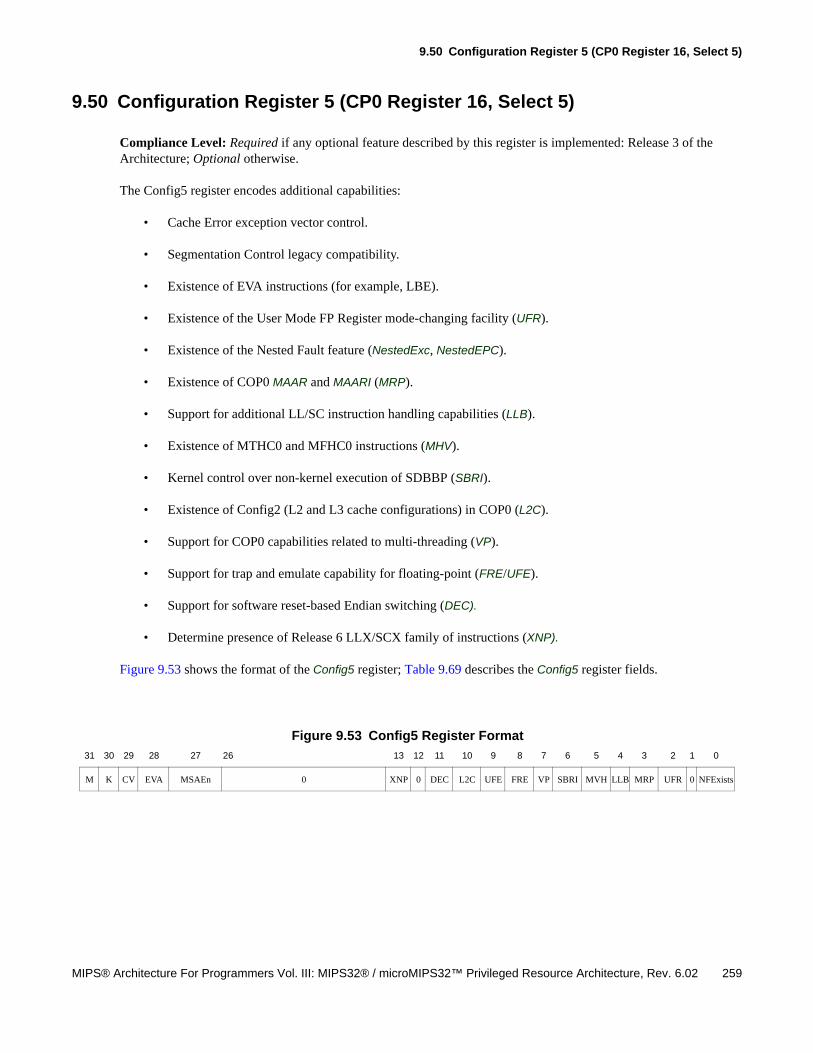
9.50 Configuration Register 5 (CP0 Register 16, Select 5)
MIPS® Architecture For Programmers Vol. III: MIPS32® / microMIPS32™ Privileged Resource Architecture, Rev. 6.02 259
9.50 Configuration Register 5 (CP0 Register 16, Select 5)
Compliance Level: Required if any optional feature described by this register is implemented: Release 3 of the Architecture; Optional otherwise.
The Config5 register encodes additional capabilities:
• Cache Error exception vector control.
• Segmentation Control legacy compatibility.
• Existence of EVA instructions (for example, LBE).
• Existence of the User Mode FP Register mode-changing facility (UFR).
• Existence of the Nested Fault feature (NestedExc, NestedEPC).
• Existence of COP0 MAAR and MAARI (MRP).
• Support for additional LL/SC instruction handling capabilities (LLB).
• Existence of MTHC0 and MFHC0 instructions (MHV).
• Kernel control over non-kernel execution of SDBBP (SBRI).
• Existence of Config2 (L2 and L3 cache configurations) in COP0 (L2C).
• Support for COP0 capabilities related to multi-threading (VP).
• Support for trap and emulate capability for floating-point (FRE/UFE).
• Support for software reset-based Endian switching (DEC).
• Determine presence of Release 6 LLX/SCX family of instructions (XNP).
Figure 9.53 shows the format of the Config5 register; Table 9.69 describes the Config5 register fields.
Figure 9.53 Config5 Register Format
31 30 29 28 27 26 13 12 11 10 9 8 7 6 5 4 3 2 1 0
M K CV EVA MSAEn 0 XNP 0 DEC L2C UFE FRE VP SBRI MVH LLB MRP UFR 0 NFExists
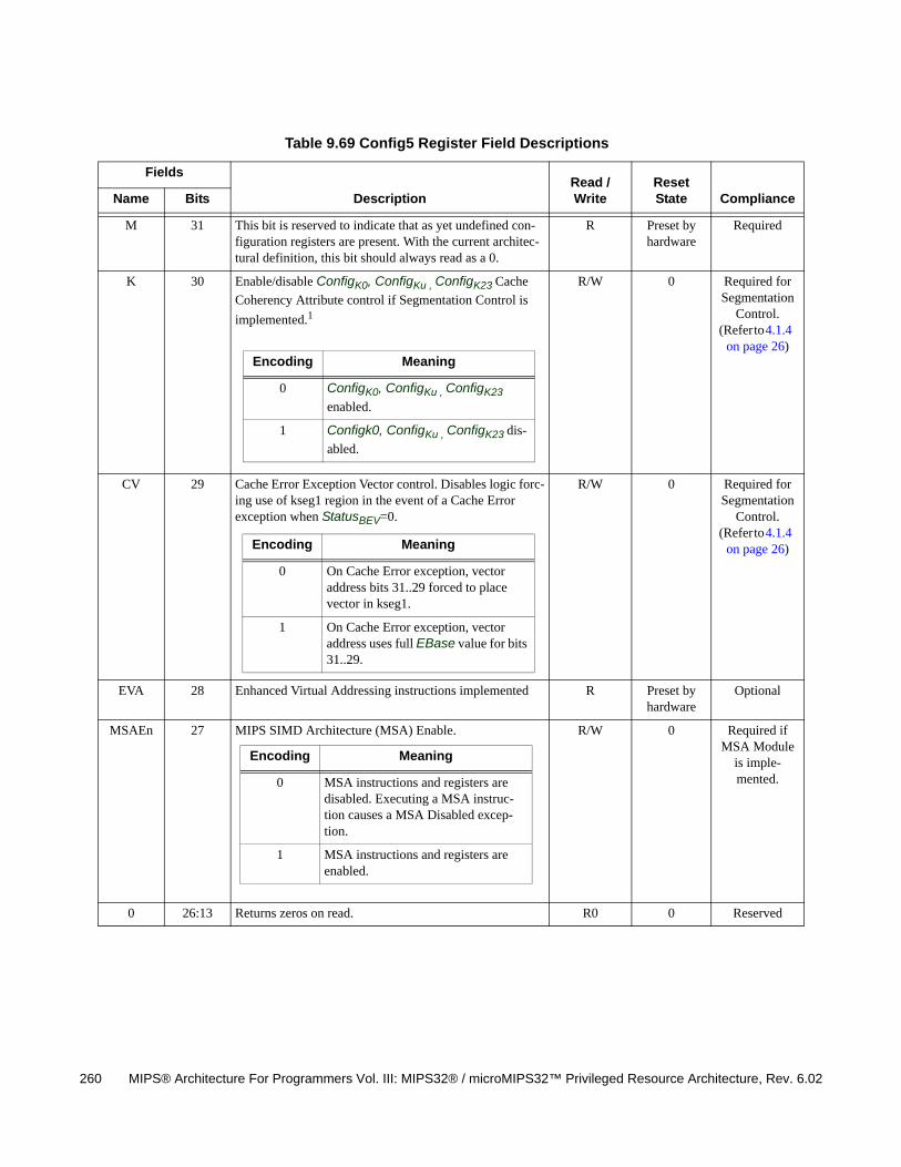
260 MIPS® Architecture For Programmers Vol. III: MIPS32® / microMIPS32™ Privileged Resource Architecture, Rev. 6.02
Table 9.69 Config5 Register Field Descriptions
Fields
DescriptionRead / Write
Reset State ComplianceName Bits
M 31 This bit is reserved to indicate that as yet undefined con-figuration registers are present. With the current architec-tural definition, this bit should always read as a 0.
R Preset by hardware
Required
K 30 Enable/disable ConfigK0, ConfigKu , ConfigK23 Cache
Coherency Attribute control if Segmentation Control is
implemented.1
R/W 0 Required for Segmentation
Control.(Refer to 4.1.4
on page 26)
CV 29 Cache Error Exception Vector control. Disables logic forc-ing use of kseg1 region in the event of a Cache Error exception when StatusBEV=0.
R/W 0 Required for Segmentation
Control.(Refer to 4.1.4
on page 26)
EVA 28 Enhanced Virtual Addressing instructions implemented R Preset by hardware
Optional
MSAEn 27 MIPS SIMD Architecture (MSA) Enable. R/W 0 Required if MSA Module
is imple-mented.
0 26:13 Returns zeros on read. R0 0 Reserved
Encoding Meaning
0 ConfigK0, ConfigKu , ConfigK23
enabled.
1 Configk0, ConfigKu , ConfigK23 dis-
abled.
Encoding Meaning
0 On Cache Error exception, vector address bits 31..29 forced to place vector in kseg1.
1 On Cache Error exception, vector address uses full EBase value for bits 31..29.
Encoding Meaning
0 MSA instructions and registers are disabled. Executing a MSA instruc-tion causes a MSA Disabled excep-tion.
1 MSA instructions and registers are enabled.
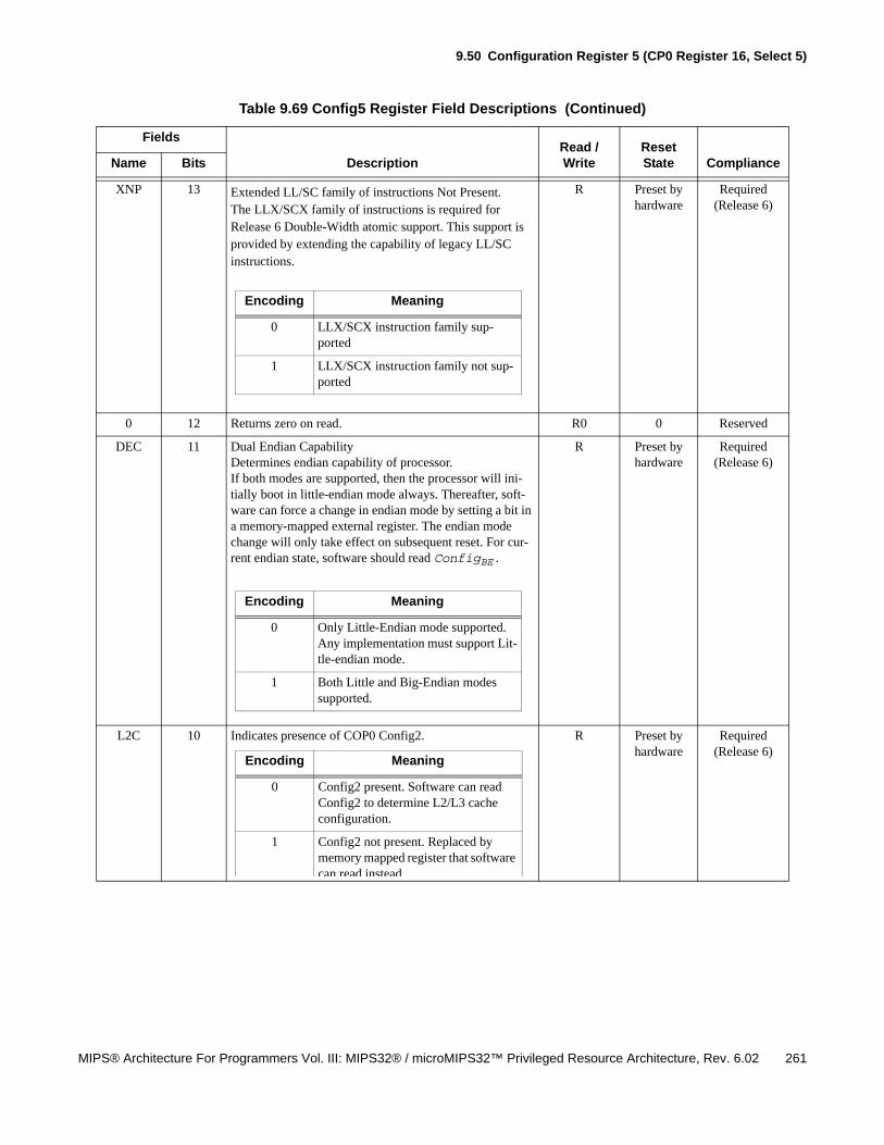
9.50 Configuration Register 5 (CP0 Register 16, Select 5)
MIPS® Architecture For Programmers Vol. III: MIPS32® / microMIPS32™ Privileged Resource Architecture, Rev. 6.02 261
XNP 13 Extended LL/SC family of instructions Not Present.The LLX/SCX family of instructions is required for Release 6 Double-Width atomic support. This support is provided by extending the capability of legacy LL/SC instructions.
R Preset by hardware
Required(Release 6)
0 12 Returns zero on read. R0 0 Reserved
DEC 11 Dual Endian CapabilityDetermines endian capability of processor. If both modes are supported, then the processor will ini-tially boot in little-endian mode always. Thereafter, soft-ware can force a change in endian mode by setting a bit in a memory-mapped external register. The endian mode change will only take effect on subsequent reset. For cur-rent endian state, software should read ConfigBE.
R Preset by hardware
Required (Release 6)
L2C 10 Indicates presence of COP0 Config2. R Preset by hardware
Required (Release 6)
Table 9.69 Config5 Register Field Descriptions (Continued)
Fields
DescriptionRead / Write
Reset State ComplianceName Bits
Encoding Meaning
0 LLX/SCX instruction family sup-ported
1 LLX/SCX instruction family not sup-ported
Encoding Meaning
0 Only Little-Endian mode supported. Any implementation must support Lit-tle-endian mode.
1 Both Little and Big-Endian modes supported.
Encoding Meaning
0 Config2 present. Software can read Config2 to determine L2/L3 cache configuration.
1 Config2 not present. Replaced by memory mapped register that software can read instead.
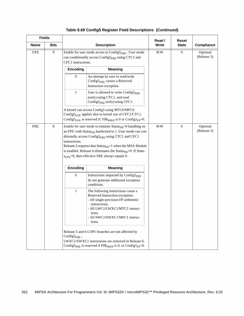
262 MIPS® Architecture For Programmers Vol. III: MIPS32® / microMIPS32™ Privileged Resource Architecture, Rev. 6.02
UFE 9 Enable for user mode access to Config5FRE . User mode
can conditionally access Config5FRE using CTC1 and
CFC1 instructions.
A kernel can access Config5 using MTC0/MFC0. Config5UFE applies also to kernel use of CFC1/CTC1.
Config5UFE is reserved if: FIRFREP is 0 or Config1FP=0.
R/W 0 Optional (Release 5)
FRE 8 Enable for user mode to emulate StatusFR=0 handling on
an FPU with StatusFR hardwired to 1. User mode can con-
ditionally access Config5FRE using CTC1 and CFC1
instructions.Release 5 requires that StatusFR=1 when the MSA Module
is enabled. Release 6 eliminates the StatusFR=0. If Statu-
sUFE=0, then effective FRE always equals 0.
Release 5 and 6 COP1 branches are not affected by Config5FRE .
LWXC1/SWXC1 instructions are removed in Release 6.Config5FRE is reserved if FIRFREP is 0, or Config1FP=0.
R/W 0 Optional (Release 5)
Table 9.69 Config5 Register Field Descriptions (Continued)
Fields
DescriptionRead / Write
Reset State ComplianceName Bits
Encoding Meaning
0 An attempt by user to read/write Config5FRE causes a Reserved
Instruction exception.
1 User is allowed to write Config5FRE
(only) using CTC1, and read Config5FRE (only) using CFC1.
Encoding Meaning
0 Instructions impacted by Config5FRE
do not generate additional exception conditions.
1 The following instructions cause a Reserved Instruction exception:- All single-precision FP arithmetic
instructions.- All LWC1/LWXC1/MTC1 instruc-
tions.- All SWC1/SWXC1/MFC1 instruc-
tions.
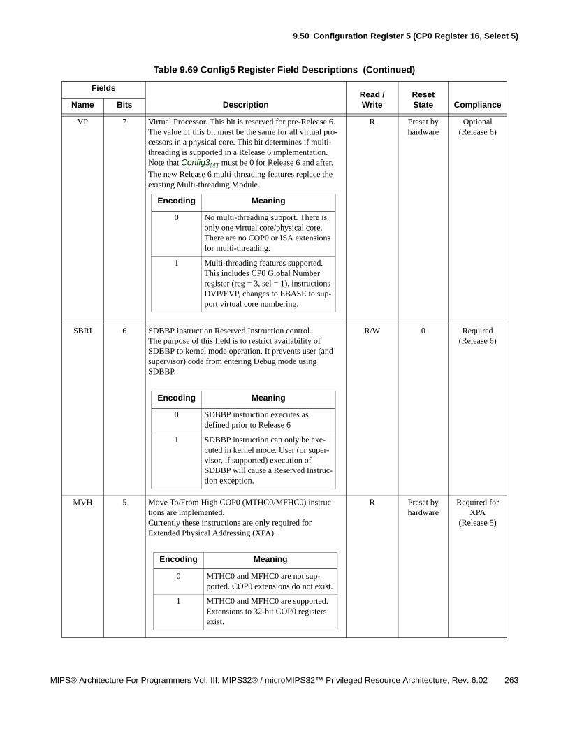
9.50 Configuration Register 5 (CP0 Register 16, Select 5)
MIPS® Architecture For Programmers Vol. III: MIPS32® / microMIPS32™ Privileged Resource Architecture, Rev. 6.02 263
VP 7 Virtual Processor. This bit is reserved for pre-Release 6. The value of this bit must be the same for all virtual pro-cessors in a physical core. This bit determines if multi-threading is supported in a Release 6 implementation. Note that Config3MT must be 0 for Release 6 and after.
The new Release 6 multi-threading features replace the existing Multi-threading Module.
R Preset by hardware
Optional (Release 6)
SBRI 6 SDBBP instruction Reserved Instruction control. The purpose of this field is to restrict availability of SDBBP to kernel mode operation. It prevents user (and supervisor) code from entering Debug mode using SDBBP.
R/W 0 Required(Release 6)
MVH 5 Move To/From High COP0 (MTHC0/MFHC0) instruc-tions are implemented.Currently these instructions are only required for Extended Physical Addressing (XPA).
R Preset by hardware
Required for XPA
(Release 5)
Table 9.69 Config5 Register Field Descriptions (Continued)
Fields
DescriptionRead / Write
Reset State ComplianceName Bits
Encoding Meaning
0 No multi-threading support. There is only one virtual core/physical core. There are no COP0 or ISA extensions for multi-threading.
1 Multi-threading features supported. This includes CP0 Global Number register (reg = 3, sel = 1), instructions DVP/EVP, changes to EBASE to sup-port virtual core numbering.
Encoding Meaning
0 SDBBP instruction executes as defined prior to Release 6
1 SDBBP instruction can only be exe-cuted in kernel mode. User (or super-visor, if supported) execution of SDBBP will cause a Reserved Instruc-tion exception.
Encoding Meaning
0 MTHC0 and MFHC0 are not sup-ported. COP0 extensions do not exist.
1 MTHC0 and MFHC0 are supported. Extensions to 32-bit COP0 registers exist.
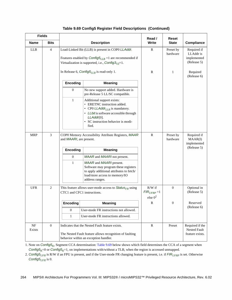
264 MIPS® Architecture For Programmers Vol. III: MIPS32® / microMIPS32™ Privileged Resource Architecture, Rev. 6.02
LLB 4 Load-Linked Bit (LLB) is present in COP0 LLAddr.
Features enabled by Config5LLB =1 are recommended if
Virtualization is supported, i.e., Config3VZ=1.
In Release 6, Config5LLB is read-only 1.
R
R
Preset by hardware
1
Required if LLAddr is
implemented (Release 5)
Required(Release 6)
MRP 3 COP0 Memory Accessibility Attribute Registers, MAAR and MAARI, are present.
R Preset by hardware
Required if MAAR(I)
implemented (Release 5)
UFR 2 This feature allows user-mode access to StatusFR using
CTC1 and CFC1 instructions.
R/W if FIRUFRP =1
else 02
R
0
0
Optional in (Release 5)
Reserved (Release 6)
NFExists
0 Indicates that the Nested Fault feature exists.
The Nested Fault feature allows recognition of faulting behavior within an exception handler.
R Preset Required if the Nested Fault feature exists.
1. Note on Config5K, Segment CCA determination: Table 9.69 below shows which field determines the CCA of a segment when
Config5K=0 or Config5K=1, on implementations with/without a TLB, when the region is accessed unmapped.
2. Config5UFR is R/W if an FPU is present, and if the User-mode FR changing feature is present, i.e. if FIRUFRP is set. Otherwise
Config5UFR is 0.
Table 9.69 Config5 Register Field Descriptions (Continued)
Fields
DescriptionRead / Write
Reset State ComplianceName Bits
Encoding Meaning
0 No new support added. Hardware is pre-Release 5 LL/SC compatible.
1 Additional support exists: • ERETNC instruction added.• CP0 LLAddrLLB is mandatory.
• LLbit is software accessible through LLAddr[0].
• SC instruction behavior is modi-fied.
Encoding Meaning
0 MAAR and MAARI not present.
1 MAAR and MAARI present. Software may program these registers to apply additional attributes to fetch/load/store access to memory/IO address ranges.
Encoding Meaning
0 User-mode FR instructions not allowed.
1 User-mode FR instructions allowed.
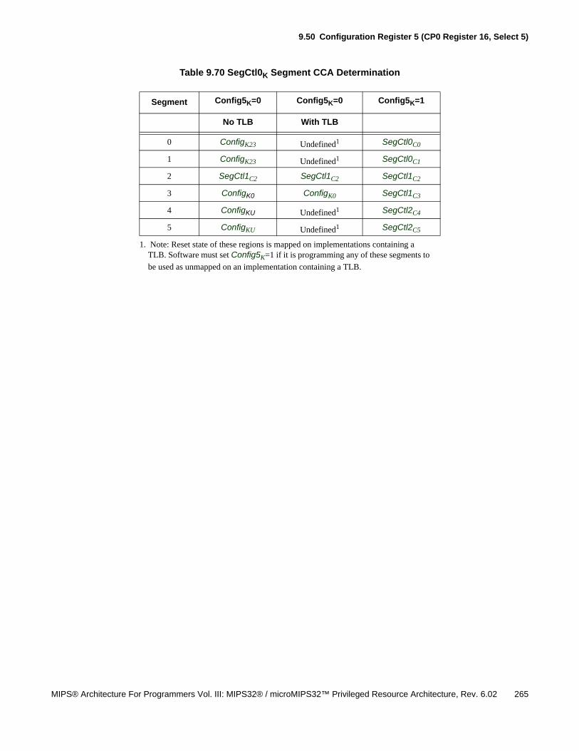
9.50 Configuration Register 5 (CP0 Register 16, Select 5)
MIPS® Architecture For Programmers Vol. III: MIPS32® / microMIPS32™ Privileged Resource Architecture, Rev. 6.02 265
Table 9.70 SegCtl0K Segment CCA Determination
Segment Config5K=0 Config5K=0 Config5K=1
No TLB With TLB
0 ConfigK23 Undefined1
1. Note: Reset state of these regions is mapped on implementations containing a TLB. Software must set Config5K=1 if it is programming any of these segments to
be used as unmapped on an implementation containing a TLB.
SegCtl0C0
1 ConfigK23 Undefined1 SegCtl0C1
2 SegCtl1C2 SegCtl1C2 SegCtl1C2
3 ConfigK0 ConfigK0 SegCtl1C3
4 ConfigKU Undefined1 SegCtl2C4
5 ConfigKU Undefined1 SegCtl2C5

266 MIPS® Architecture For Programmers Vol. III: MIPS32® / microMIPS32™ Privileged Resource Architecture, Rev. 6.02
9.51 Reserved for Implementations (CP0 Register 16, Selects 6 and 7)
MIPS® Architecture For Programmers Vol. III: MIPS32® / microMIPS32™ Privileged Resource Architecture, Rev. 6.02 267
9.51 Reserved for Implementations (CP0 Register 16, Selects 6 and 7)
Compliance Level: Implementation Dependent.
CP0 register 16, Selects 6 and 7 are reserved for implementation-dependent use and is not defined by the architecture. In order to use CP0 register 16, Selects 6 and 7, it is not necessary to implement CP0 register 16, Selects 2 through 5 only to set the M bit in each of these registers. That is, if the Config2 and Config3 registers are not needed for the implementation, they need not be implemented just to provide the M bits.
The architecture only defines the use of the M bits for presence detection of Selects 1 to 5.

268 MIPS® Architecture For Programmers Vol. III: MIPS32® / microMIPS32™ Privileged Resource Architecture, Rev. 6.02
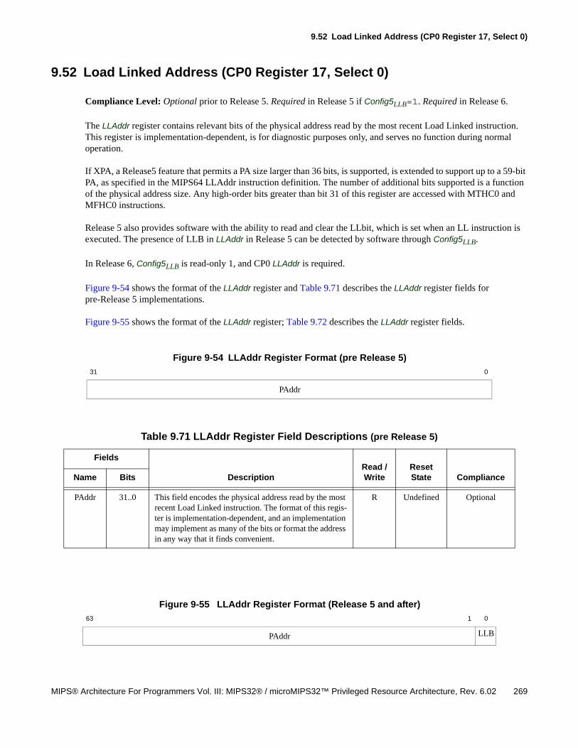
9.52 Load Linked Address (CP0 Register 17, Select 0)
MIPS® Architecture For Programmers Vol. III: MIPS32® / microMIPS32™ Privileged Resource Architecture, Rev. 6.02 269
9.52 Load Linked Address (CP0 Register 17, Select 0)
Compliance Level: Optional prior to Release 5. Required in Release 5 if Config5LLB=1. Required in Release 6.
The LLAddr register contains relevant bits of the physical address read by the most recent Load Linked instruction. This register is implementation-dependent, is for diagnostic purposes only, and serves no function during normal operation.
If XPA, a Release5 feature that permits a PA size larger than 36 bits, is supported, is extended to support up to a 59-bit PA, as specified in the MIPS64 LLAddr instruction definition. The number of additional bits supported is a function of the physical address size. Any high-order bits greater than bit 31 of this register are accessed with MTHC0 and MFHC0 instructions.
Release 5 also provides software with the ability to read and clear the LLbit, which is set when an LL instruction is executed. The presence of LLB in LLAddr in Release 5 can be detected by software through Config5LLB.
In Release 6, Config5LLB is read-only 1, and CP0 LLAddr is required.
Figure 9-54 shows the format of the LLAddr register and Table 9.71 describes the LLAddr register fields for pre-Release 5 implementations.
Figure 9-55 shows the format of the LLAddr register; Table 9.72 describes the LLAddr register fields.
Figure 9-54 LLAddr Register Format (pre Release 5)
31 0
PAddr
Table 9.71 LLAddr Register Field Descriptions (pre Release 5)
Fields
DescriptionRead / Write
Reset State ComplianceName Bits
PAddr 31..0 This field encodes the physical address read by the most recent Load Linked instruction. The format of this regis-ter is implementation-dependent, and an implementation may implement as many of the bits or format the address in any way that it finds convenient.
R Undefined Optional
Figure 9-55 LLAddr Register Format (Release 5 and after)
63 1 0
PAddr LLB
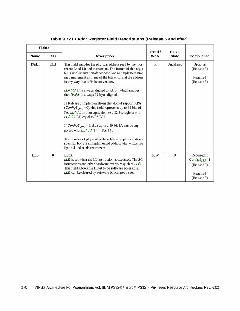
270 MIPS® Architecture For Programmers Vol. III: MIPS32® / microMIPS32™ Privileged Resource Architecture, Rev. 6.02
Table 9.72 LLAddr Register Field Descriptions (Release 5 and after)
Fields
DescriptionRead / Write
Reset State ComplianceName Bits
PAddr 63..1 This field encodes the physical address read by the most recent Load Linked instruction. The format of this regis-ter is implementation-dependent, and an implementation may implement as many of the bits or format the address in any way that it finds convenient.
LLAddr[1] is always aligned to PA[5], which implies that PAddr is always 32-byte aligned.
In Release 5 implementations that do not support XPA (Config3LPA = 0), this field represents up to 36 bits of
PA. LLAddr is then equivalent to a 32-bit register with LLAddr[31] equal to PA[35].
If Config3LPA = 1, then up to a 59-bit PA can be sup-
ported with LLAddr[54] = PA[59].
The number of physical address bits is implementation- specific. For the unimplemented address bits, writes are ignored and reads return zero.
R Undefined Optional(Release 5)
Required(Release 6)
LLB 0 LLbit. LLB is set when the LL instruction is executed. The SC instructions and other hardware events may clear LLB. This field allows the LLbit to be software accessible. LLB can be cleared by software but cannot be set.
R/W 0 Required if Config5LLB=1
(Release 5)
Required(Release 6)
9.53 Memory Accessibility Attribute Register (CP0 Register 17, Select 1)
MIPS® Architecture For Programmers Vol. III: MIPS32® / microMIPS32™ Privileged Resource Architecture, Rev. 6.02 271
9.53 Memory Accessibility Attribute Register (CP0 Register 17, Select 1)
Compliance Level: Optional (Release 5)
The MAAR register is a read/write register included in Release 5 of the architecture that defines the accessibility attri-butes of physical address regions. In particular, MAAR defines whether an instruction fetch or data load can specula-tively access a memory region within the physical address bounds specified by MAAR.
If the MAAR function yields a valid attribute, it will only override any equivalent attribute determined through other means, if it provides a more conservative outcome. For example, if the MMU yields a cacheable CCA, but MAAR yields a speculate attribute set to 0, then the access should not speculate as determined by the MAAR result. Similarly, if the MMU yields an uncacheable CCA, but MAAR yields a speculate attribute set to 1, then the access should not speculate.
In Release 5, the CCA of a access now defines speculation, along with MAAR. An access with a cacheable CCA is allowed to speculate. An access with uncacheable CCA is not allowed to speculate unless the uncacheable CCA=7 (UCA) is used. The final speculative attribute is a combination of the CCA and MAAR as described above.
The address range specified by a MAAR may be used to specify an attribute for any region of the address space, whether memory (DRAM) or memory-mapped I/O.
MAAR is impacted by Extended Physical Addressing (XPA), a Release 5 feature, if included. If XPA is supported, then MAAR must be extended by additional physical address bits. To maintain atomicity of the write to an extended MAAR, two valid bits, VL and VH, are required. The use of both bits is conditional on PageGrainELPA. While a write
to the upper half of the extended could precede the write to the lower half to maintain atomicity, the required property of MTC0 to zero out extended PA bits prevents software from using this method.
It is recommended that Release 5 implementations of the architecture include the MAAR feature to allow architectural instead of implementation-dependent definition of speculation.
The Release 5 specification of MAAR requires that MAAR registers be paired, i.e., one specifies an upper bounds of the address range, and the other the lower bound. Future extensions to this specification may allow the flexibility of not pairing registers to allow fewer registers to be implemented with contiguous address ranges but different attribute types.
MAAR must be implemented in conjunction with MAARI (MAAR Index, CP0 Register 17, Sel 2). MAARI must be ini-tialized with the appropriate MAARI register number before the MAAR is accessed with an MTC0 or MFC0. An EHB instruction is required to be placed between the write to MAAR Index and subsequent execution of MTC0 or MFC0 that specifies MAAR.
The presence of MAAR can be detected by software through Config5MRP.
Figure 9-56 shows the format of the MAAR register; Table 9.73 describes the MAAR register fields.
Operation:
The pseudocode below shows a 3-pair MAAR implementation to determine speculation. It is recommended that implementations follow this description to enable portable software. As described, software must set the logical valid to 1 of each register of the pair to enable a MAAR pair. It may, however, clear any one logical valid of the pair to inval-idate the whole MAAR pair. Once both logical valids are set to 1, hardware factors in the speculate attribute of only the upper MAAR register with even index. The logical valid is determined as described in the pseudo-code below.
272 MIPS® Architecture For Programmers Vol. III: MIPS32® / microMIPS32™ Privileged Resource Architecture, Rev. 6.02
speculateCCA 0 // default is not to speculate// Modify speculate attribute as per CCA of memory access (Release 5)// Release 5: cached CCA and UCA speculatesif ((CCA == “cached”) or (CCA == “uncached-accelerated(UCA)”))
speculateCCA 1endif
// Now factor in MAARMAARmatch 0speculateMAAR 1// Example of 40-bit PA is 64KB alignedPA_Align PA[39:16]for (i=0; i<6; i=i+2) // assume 3 pairs
//Factor in XPA {Extended Physical Addressing}(MAAR[i]V = MAAR[i]VL and (MAAR[i]VH or not PageGrainELPA)(MAAR[i+1]V = MAAR[i+1]VL and (MAAR[i+1]VH or not PageGrainELPA)if (MAAR[i]V = MAAR[i+1]V // both logical valids must be set to 1
if ((MAAR[i][35:12] >= PA_Align) && // upper bound(MAAR[i+1][35:12] <= PA_Align)) // lower bound
speculateMAAR speculateMAAR and MAAR[i]S MAARmatch 1
endifendif
endfor
// if no MAAR is valid, or no MAAR match occurs, then speculateMAAR 0, speculate speculateMAAR, and speculateCCA and MAARmatch
Programming Notes:
The purpose of MAAR is to control speculation on load or fetch access to memory and IO address. A load is consid-ered speculative if it accesses memory prior to its being the oldest instsruction to retire. A fetch typically always spec-ulates on access to memory, while never speculating to IO. For implementations that support load or fetch speculation, support and initialization of MAAR is a requirement.
MAAR, as defined, has the following properties.
• If all MAAR instaces are invalid, then no speculation is allowed. This allows the MAAR initialization to occur at any point of time without the risk of execution speculative (bad path) loads or fetches from issuing to IO addresses, with the tradeoff possibly being lower performance.
• If any MAAR region enables speculation, accesses to physical addresses outside this MAAR region must be non-speculative, unless the physical address of the access matches against a MAAR region with speculation enabled. This access then can speculate.
• MAAR overlap is allowed. This allows non-speculative MAAR regions to overlap a speculative MAAR region. For example, with this property, a non-speculative region can be overlayed on a speculative DRAM region with the use of just two MAAR pairs.
For software to enable a speculative region out of reset, it first should initialize MAAR[31:0], then MAAR[63:32], assuming XPA is supported and to be enabled.
Software must follow the described method for reprogramming the state of a MAAR pair. The example assumes XPA is supported.
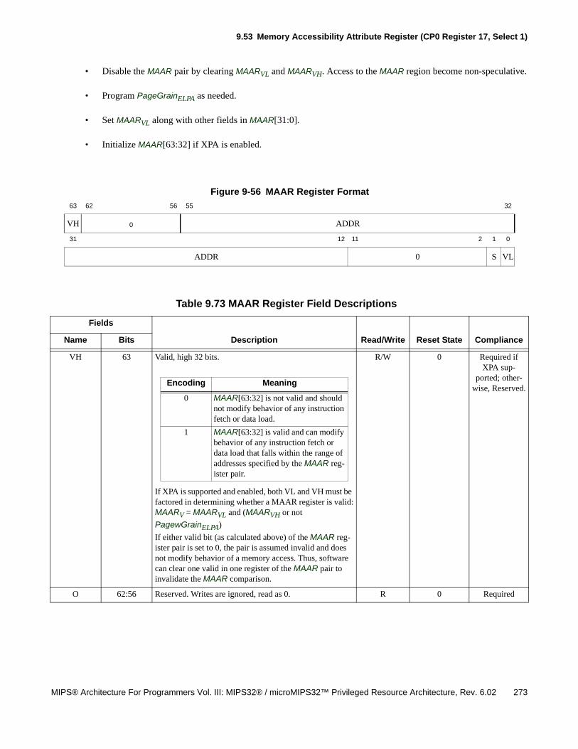
9.53 Memory Accessibility Attribute Register (CP0 Register 17, Select 1)
MIPS® Architecture For Programmers Vol. III: MIPS32® / microMIPS32™ Privileged Resource Architecture, Rev. 6.02 273
• Disable the MAAR pair by clearing MAARVL and MAARVH. Access to the MAAR region become non-speculative.
• Program PageGrainELPA as needed.
• Set MAARVL along with other fields in MAAR[31:0].
• Initialize MAAR[63:32] if XPA is enabled.
Figure 9-56 MAAR Register Format
63 62 56 55 32
VH 0 ADDR
31 12 11 2 1 0
ADDR 0 S VL
Table 9.73 MAAR Register Field Descriptions
Fields
Description Read/Write Reset State ComplianceName Bits
VH 63 Valid, high 32 bits.
If XPA is supported and enabled, both VL and VH must be factored in determining whether a MAAR register is valid:MAARV = MAARVL and (MAARVH or not
PagewGrainELPA)
If either valid bit (as calculated above) of the MAAR reg-ister pair is set to 0, the pair is assumed invalid and does not modify behavior of a memory access. Thus, software can clear one valid in one register of the MAAR pair to invalidate the MAAR comparison.
R/W 0 Required if XPA sup-
ported; other-wise, Reserved.
O 62:56 Reserved. Writes are ignored, read as 0. R 0 Required
Encoding Meaning
0 MAAR[63:32] is not valid and should not modify behavior of any instruction fetch or data load.
1 MAAR[63:32] is valid and can modify behavior of any instruction fetch or data load that falls within the range of addresses specified by the MAAR reg-ister pair.
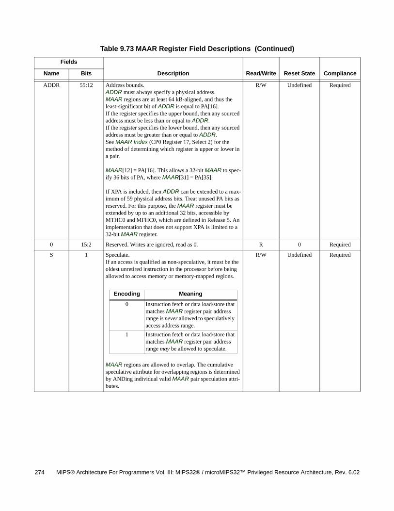
274 MIPS® Architecture For Programmers Vol. III: MIPS32® / microMIPS32™ Privileged Resource Architecture, Rev. 6.02
ADDR 55:12 Address bounds. ADDR must always specify a physical address.MAAR regions are at least 64 kB-aligned, and thus the least-significant bit of ADDR is equal to PA[16].If the register specifies the upper bound, then any sourced address must be less than or equal to ADDR.If the register specifies the lower bound, then any sourced address must be greater than or equal to ADDR.See MAAR Index (CP0 Register 17, Select 2) for the method of determining which register is upper or lower in a pair.
MAAR[12] = PA[16]. This allows a 32-bit MAAR to spec-ify 36 bits of PA, where MAAR[31] = PA[35].
If XPA is included, then ADDR can be extended to a max-imum of 59 physical address bits. Treat unused PA bits as reserved. For this purpose, the MAAR register must be extended by up to an additional 32 bits, accessible by MTHC0 and MFHC0, which are defined in Release 5. An implementation that does not support XPA is limited to a 32-bit MAAR register.
R/W Undefined Required
0 15:2 Reserved. Writes are ignored, read as 0. R 0 Required
S 1 Speculate. If an access is qualified as non-speculative, it must be the oldest unretired instruction in the processor before being allowed to access memory or memory-mapped regions.
MAAR regions are allowed to overlap. The cumulative speculative attribute for overlapping regions is determined by ANDing individual valid MAAR pair speculation attri-butes.
R/W Undefined Required
Table 9.73 MAAR Register Field Descriptions (Continued)
Fields
Description Read/Write Reset State ComplianceName Bits
Encoding Meaning
0 Instruction fetch or data load/store that matches MAAR register pair address range is never allowed to speculatively access address range.
1 Instruction fetch or data load/store that matches MAAR register pair address range may be allowed to speculate.
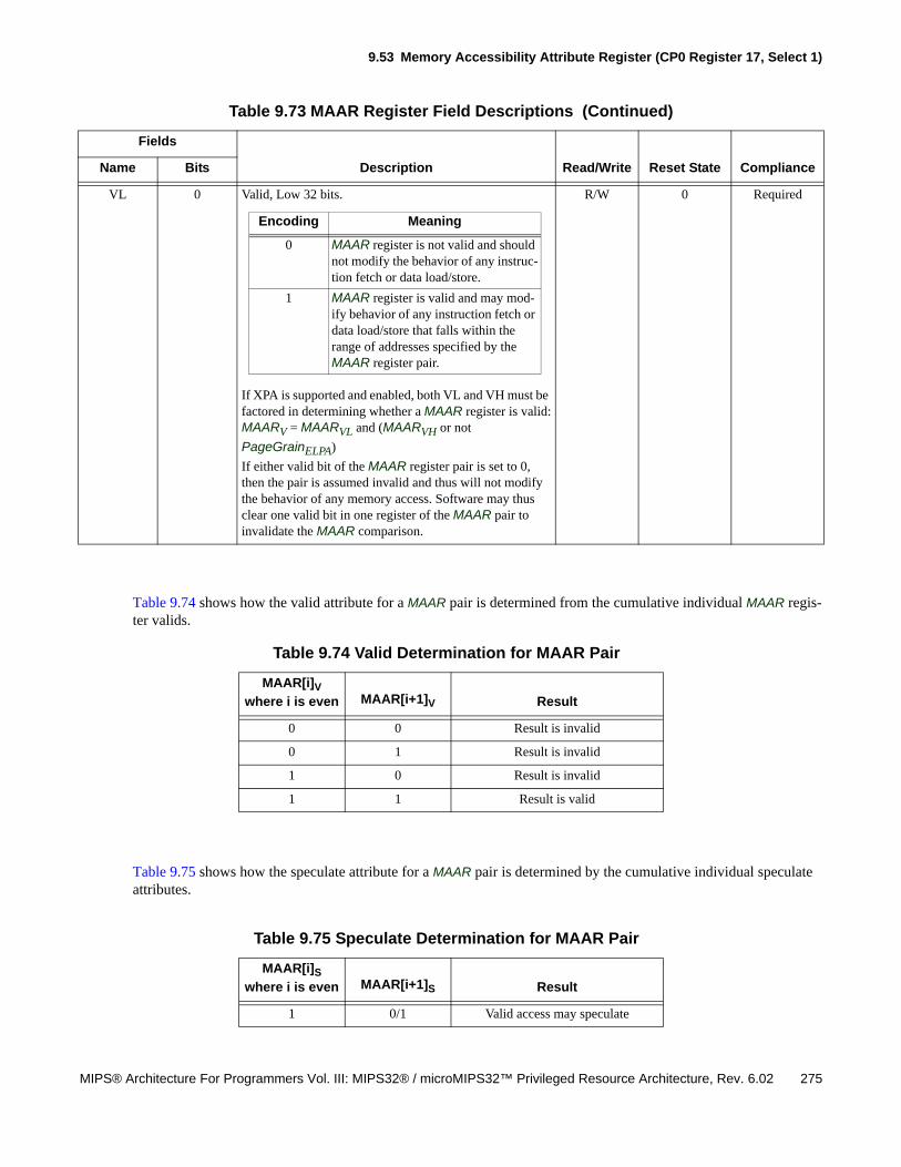
9.53 Memory Accessibility Attribute Register (CP0 Register 17, Select 1)
MIPS® Architecture For Programmers Vol. III: MIPS32® / microMIPS32™ Privileged Resource Architecture, Rev. 6.02 275
Table 9.74 shows how the valid attribute for a MAAR pair is determined from the cumulative individual MAAR regis-ter valids.
Table 9.75 shows how the speculate attribute for a MAAR pair is determined by the cumulative individual speculate attributes.
VL 0 Valid, Low 32 bits.
If XPA is supported and enabled, both VL and VH must be factored in determining whether a MAAR register is valid:MAARV = MAARVL and (MAARVH or not
PageGrainELPA)
If either valid bit of the MAAR register pair is set to 0, then the pair is assumed invalid and thus will not modify the behavior of any memory access. Software may thus clear one valid bit in one register of the MAAR pair to invalidate the MAAR comparison.
R/W 0 Required
Table 9.74 Valid Determination for MAAR Pair
MAAR[i]V
where i is even MAAR[i+1]V Result
0 0 Result is invalid
0 1 Result is invalid
1 0 Result is invalid
1 1 Result is valid
Table 9.75 Speculate Determination for MAAR Pair
MAAR[i]S
where i is even MAAR[i+1]S Result
1 0/1 Valid access may speculate
Table 9.73 MAAR Register Field Descriptions (Continued)
Fields
Description Read/Write Reset State ComplianceName Bits
Encoding Meaning
0 MAAR register is not valid and should not modify the behavior of any instruc-tion fetch or data load/store.
1 MAAR register is valid and may mod-ify behavior of any instruction fetch or data load/store that falls within the range of addresses specified by the MAAR register pair.
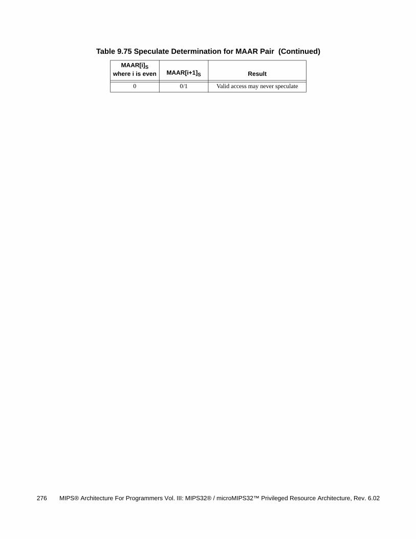
276 MIPS® Architecture For Programmers Vol. III: MIPS32® / microMIPS32™ Privileged Resource Architecture, Rev. 6.02
0 0/1 Valid access may never speculate
Table 9.75 Speculate Determination for MAAR Pair (Continued)
MAAR[i]S
where i is even MAAR[i+1]S Result
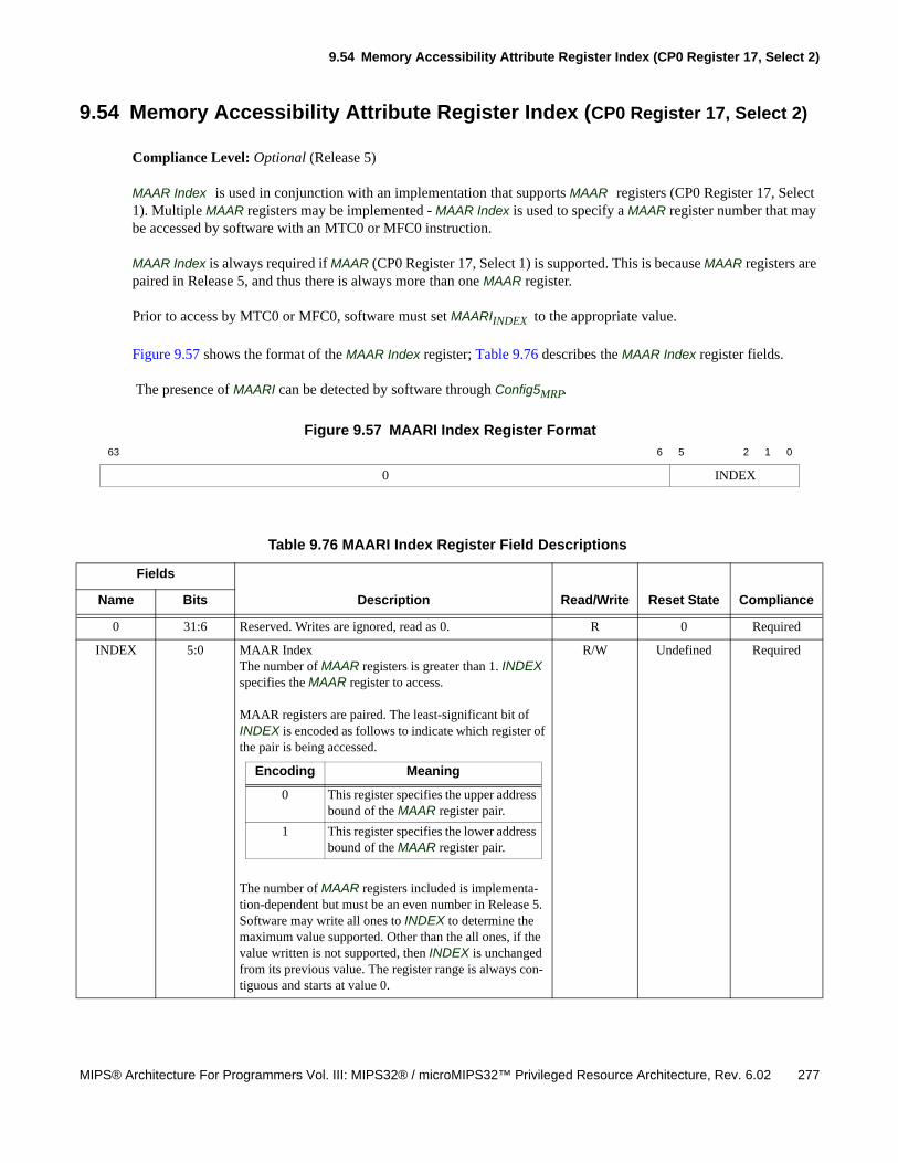
9.54 Memory Accessibility Attribute Register Index (CP0 Register 17, Select 2)
MIPS® Architecture For Programmers Vol. III: MIPS32® / microMIPS32™ Privileged Resource Architecture, Rev. 6.02 277
9.54 Memory Accessibility Attribute Register Index (CP0 Register 17, Select 2)
Compliance Level: Optional (Release 5)
MAAR Index is used in conjunction with an implementation that supports MAAR registers (CP0 Register 17, Select 1). Multiple MAAR registers may be implemented - MAAR Index is used to specify a MAAR register number that may be accessed by software with an MTC0 or MFC0 instruction.
MAAR Index is always required if MAAR (CP0 Register 17, Select 1) is supported. This is because MAAR registers are paired in Release 5, and thus there is always more than one MAAR register.
Prior to access by MTC0 or MFC0, software must set MAARIINDEX to the appropriate value.
Figure 9.57 shows the format of the MAAR Index register; Table 9.76 describes the MAAR Index register fields.
The presence of MAARI can be detected by software through Config5MRP.
Figure 9.57 MAARI Index Register Format
63 6 5 2 1 0
0 INDEX
Table 9.76 MAARI Index Register Field Descriptions
Fields
Description Read/Write Reset State ComplianceName Bits
0 31:6 Reserved. Writes are ignored, read as 0. R 0 Required
INDEX 5:0 MAAR IndexThe number of MAAR registers is greater than 1. INDEX specifies the MAAR register to access.
MAAR registers are paired. The least-significant bit of INDEX is encoded as follows to indicate which register of the pair is being accessed.
The number of MAAR registers included is implementa-tion-dependent but must be an even number in Release 5. Software may write all ones to INDEX to determine the maximum value supported. Other than the all ones, if the value written is not supported, then INDEX is unchanged from its previous value. The register range is always con-tiguous and starts at value 0.
R/W Undefined Required
Encoding Meaning
0 This register specifies the upper address bound of the MAAR register pair.
1 This register specifies the lower address bound of the MAAR register pair.

278 MIPS® Architecture For Programmers Vol. III: MIPS32® / microMIPS32™ Privileged Resource Architecture, Rev. 6.02
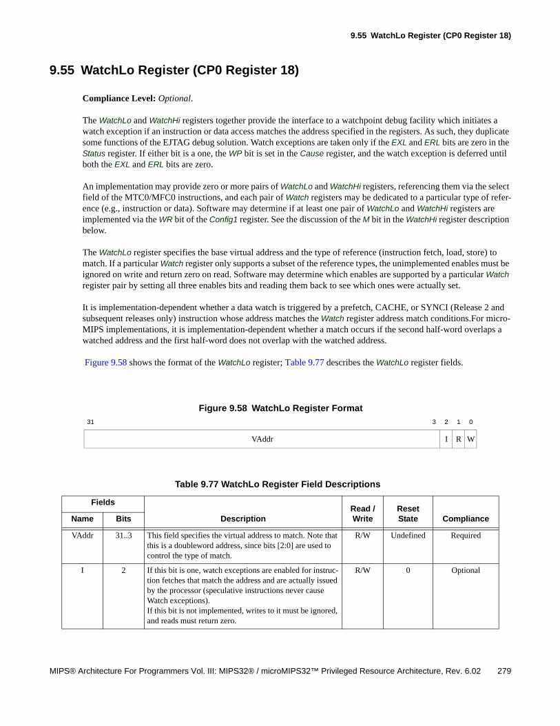
9.55 WatchLo Register (CP0 Register 18)
MIPS® Architecture For Programmers Vol. III: MIPS32® / microMIPS32™ Privileged Resource Architecture, Rev. 6.02 279
9.55 WatchLo Register (CP0 Register 18)
Compliance Level: Optional.
The WatchLo and WatchHi registers together provide the interface to a watchpoint debug facility which initiates a watch exception if an instruction or data access matches the address specified in the registers. As such, they duplicate some functions of the EJTAG debug solution. Watch exceptions are taken only if the EXL and ERL bits are zero in the Status register. If either bit is a one, the WP bit is set in the Cause register, and the watch exception is deferred until both the EXL and ERL bits are zero.
An implementation may provide zero or more pairs of WatchLo and WatchHi registers, referencing them via the select field of the MTC0/MFC0 instructions, and each pair of Watch registers may be dedicated to a particular type of refer-ence (e.g., instruction or data). Software may determine if at least one pair of WatchLo and WatchHi registers are implemented via the WR bit of the Config1 register. See the discussion of the M bit in the WatchHi register description below.
The WatchLo register specifies the base virtual address and the type of reference (instruction fetch, load, store) to match. If a particular Watch register only supports a subset of the reference types, the unimplemented enables must be ignored on write and return zero on read. Software may determine which enables are supported by a particular Watch register pair by setting all three enables bits and reading them back to see which ones were actually set.
It is implementation-dependent whether a data watch is triggered by a prefetch, CACHE, or SYNCI (Release 2 and subsequent releases only) instruction whose address matches the Watch register address match conditions.For micro-MIPS implementations, it is implementation-dependent whether a match occurs if the second half-word overlaps a watched address and the first half-word does not overlap with the watched address.
Figure 9.58 shows the format of the WatchLo register; Table 9.77 describes the WatchLo register fields.
Figure 9.58 WatchLo Register Format
31 3 2 1 0
VAddr I R W
Table 9.77 WatchLo Register Field Descriptions
Fields
DescriptionRead / Write
Reset State ComplianceName Bits
VAddr 31..3 This field specifies the virtual address to match. Note that this is a doubleword address, since bits [2:0] are used to control the type of match.
R/W Undefined Required
I 2 If this bit is one, watch exceptions are enabled for instruc-tion fetches that match the address and are actually issued by the processor (speculative instructions never cause Watch exceptions).If this bit is not implemented, writes to it must be ignored, and reads must return zero.
R/W 0 Optional
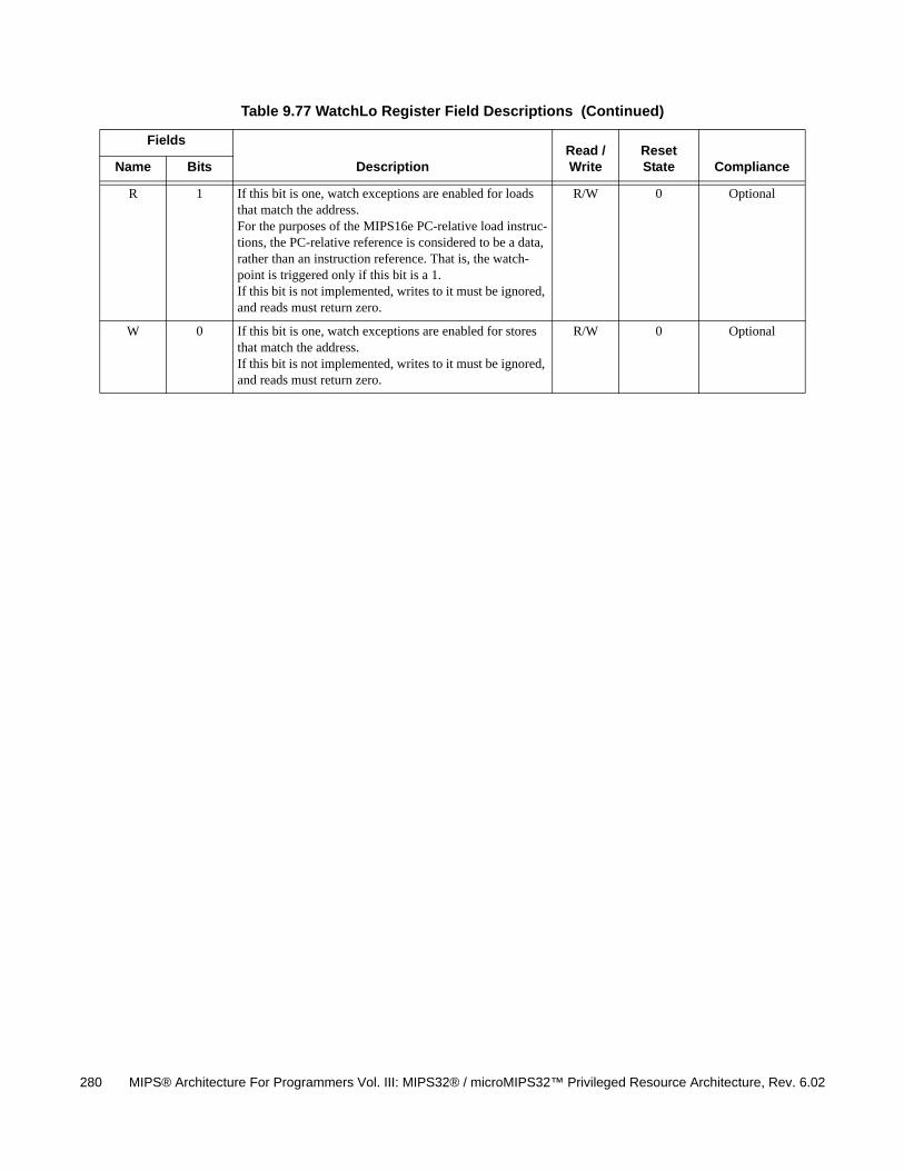
280 MIPS® Architecture For Programmers Vol. III: MIPS32® / microMIPS32™ Privileged Resource Architecture, Rev. 6.02
R 1 If this bit is one, watch exceptions are enabled for loads that match the address.For the purposes of the MIPS16e PC-relative load instruc-tions, the PC-relative reference is considered to be a data, rather than an instruction reference. That is, the watch-point is triggered only if this bit is a 1.If this bit is not implemented, writes to it must be ignored, and reads must return zero.
R/W 0 Optional
W 0 If this bit is one, watch exceptions are enabled for stores that match the address.If this bit is not implemented, writes to it must be ignored, and reads must return zero.
R/W 0 Optional
Table 9.77 WatchLo Register Field Descriptions (Continued)
Fields
DescriptionRead / Write
Reset State ComplianceName Bits
9.56 WatchHi Register (CP0 Register 19)
MIPS® Architecture For Programmers Vol. III: MIPS32® / microMIPS32™ Privileged Resource Architecture, Rev. 6.02 281
9.56 WatchHi Register (CP0 Register 19)
Compliance Level: Optional.
The WatchLo and WatchHi registers together provide the interface to a watchpoint debug facility which initiates a watch exception if an instruction or data access matches the address specified in the registers. As such, they duplicate some functions of the EJTAG debug solution. Watch exceptions are taken only if the EXL and ERL bits are zero in the Status register. If either bit is a one, the WP bit is set in the Cause register, and the watch exception is deferred until both the EXL and ERL bits are zero.
An implementation may provide zero or more pairs of WatchLo and WatchHi registers, referencing them via the select field of the MTC0/MFC0 instructions, and each pair of Watch registers may be dedicated to a particular type of refer-ence (e.g., instruction or data). Software may determine if at least one pair of WatchLo and WatchHi registers are implemented via the WR bit of the Config1 register. If the M bit is one in the WatchHi register reference with a select field of ‘n’, another WatchHi/WatchLo pair is implemented with a select field of ‘n+1’.
The WatchHi register contains information that qualifies the virtual address specified in the WatchLo register: an ASID, a G(lobal) bit, an optional address mask, and three bits (I, R, and W) that denote the condition that caused the watch register to match. If the G bit is one, any virtual address reference that matches the specified address will cause a watch exception. If the G bit is a zero, only those virtual address references for which the ASID value in the WatchHi register matches the ASID value in the EntryHi register cause a watch exception. The optional mask field provides address masking to qualify the address specified in WatchLo.
The I, R, and W bits are set by the processor when the corresponding watch register condition is satisfied and indicate which watch register pair (if more than one is implemented) and which condition matched. When set by the proces-sor, each of these bits remain set until cleared by software. All three bits are “write one to clear”, such that software must write a one to the bit in order to clear its value. The typical way to do this is to write the value read from the WatchHi register back to WatchHi. In doing so, only those bits which were set when the register was read are cleared when the register is written back.
Figure 9.59 shows the format of the WatchHi register; Table 9.78 describes the WatchHi register fields.
Figure 9.59 WatchHi Register Format
31 30 29 28 27 26 25 24 23 16 15 12 11 3 2 1 0
M G WM 0 EAS ASID 0 Mask I R W
Table 9.78 WatchHi Register Field Descriptions
Fields
DescriptionRead / Write
Reset State ComplianceName Bits
M 31 If this bit is one, another pair of WatchHi/WatchLo regis-ters is implemented at an MTC0 or MFC0 select field value of ‘n+1’
R Preset Required
282 MIPS® Architecture For Programmers Vol. III: MIPS32® / microMIPS32™ Privileged Resource Architecture, Rev. 6.02
G 30 If this bit is one, any address that matches that specified in the WatchLo register will cause a watch exception. If this bit is zero, the ASID field of the WatchHi register must match the ASID field of the EntryHi register to cause a watch exception.
R/W Undefined Required
WM 29:28 Reserved for Virtualization Module. 0 0 Reserved
EAS 25:24 If Config4AE = 1 then these bits extend the ASID field of
this register.
If Config4AE = 0 then Must be written as zero; returns
zero on read.
If Config4A
E = 1 then
R/Welse 0
If Config4AE =
1 then
Undefinedelse 0
Required
ASID 23..16 ASID value which is required to match that in the EntryHi register if the G bit is zero in the WatchHi register.
R/W Undefined Required
Mask 11..3 Optional bit mask that qualifies the address in the WatchLo register. If this field is implemented, any bit in this field that is a one inhibits the corresponding address bit from participating in the address match.If this field is not implemented, writes to it must be ignored, and reads must return zero.Software may determine how many mask bits are imple-mented by writing ones the this field and then reading back the result.
R/W Undefined Optional
I 2 This bit is set by hardware when an instruction fetch con-dition matches the values in this watch register pair. When set, the bit remains set until cleared by software, which is accomplished by writing a 1 to the bit.
W1C Undefined Required (Release 2)
R 1 This bit is set by hardware when a load condition matches the values in this watch register pair. When set, the bit remains set until cleared by software, which is accom-plished by writing a 1 to the bit.
W1C Undefined Required (Release 2)
W 0 This bit is set by hardware when a store condition matches the values in this watch register pair. When set, the bit remains set until cleared by software, which is accom-plished by writing a 1 to the bit.
W1C Undefined Required (Release 2)
0 27..26, 15..12
Must be written as zero; returns zero on read. 0 0 Reserved
Table 9.78 WatchHi Register Field Descriptions (Continued)
Fields
DescriptionRead / Write
Reset State ComplianceName Bits
9.57 Reserved for Implementations (CP0 Register 22, all Select values)
MIPS® Architecture For Programmers Vol. III: MIPS32® / microMIPS32™ Privileged Resource Architecture, Rev. 6.02 283
9.57 Reserved for Implementations (CP0 Register 22, all Select values)
Compliance Level: Implementation Dependent.
CP0 register 22 is reserved for implementation-dependent use and is not defined by the architecture.

284 MIPS® Architecture For Programmers Vol. III: MIPS32® / microMIPS32™ Privileged Resource Architecture, Rev. 6.02
9.58 Debug Register (CP0 Register 23, Select 0)
MIPS® Architecture For Programmers Vol. III: MIPS32® / microMIPS32™ Privileged Resource Architecture, Rev. 6.02 285
9.58 Debug Register (CP0 Register 23, Select 0)
Compliance Level: Optional.
The Debug register is part of the EJTAG specification. Refer to that specification for the format and description of this register.

286 MIPS® Architecture For Programmers Vol. III: MIPS32® / microMIPS32™ Privileged Resource Architecture, Rev. 6.02
9.59 Debug2 Register (CP0 Register 23, Select 6)
MIPS® Architecture For Programmers Vol. III: MIPS32® / microMIPS32™ Privileged Resource Architecture, Rev. 6.02 287
9.59 Debug2 Register (CP0 Register 23, Select 6)
Compliance Level: Optional.
The Debug2 register is part of the EJTAG specification. Refer to that specification for the format and description of this register.

288 MIPS® Architecture For Programmers Vol. III: MIPS32® / microMIPS32™ Privileged Resource Architecture, Rev. 6.02
9.60 DEPC Register (CP0 Register 24)
MIPS® Architecture For Programmers Vol. III: MIPS32® / microMIPS32™ Privileged Resource Architecture, Rev. 6.02 289
9.60 DEPC Register (CP0 Register 24)
Compliance Level: Optional.
The DEPC register is a read-write register that contains the address at which processing resumes after a debug excep-tion has been serviced. It is part of the EJTAG specification and the reader is referred there for the format and descrip-tion of the register. All bits of the DEPC register are significant and must be writable.
When a debug exception occurs, the processor writes the DEPC register with,
• the virtual address of the instruction that was the direct cause of the exception, or
• the virtual address of the immediately preceding branch or jump instruction, when the exception causing instruc-tion is in a branch delay slot, and the Branch Delay bit in the Cause register is set.
The processor reads the DEPC register as the result of execution of the DERET instruction.
Software may write the DEPC register to change the processor resume address and read the DEPC register to deter-mine at what address the processor will resume.
9.60.1 Special Handling of the DEPC Register in Processors That Implement the MIPS16e ASE or microMIPS32 Base Architecture
In processors that implement the MIPS16e ASE or the microMIPS32 base architecture, the DEPC register requires special handling.
When the processor writes the DEPC register, it combines the address at which processing resumes with the value of the ISA Mode register:
DEPC resumePC31..1 ISAMode0
“resumePC” is the address at which processing resumes, as described above.
When the processor reads the DEPC register, it distributes the bits to the PC and ISA Mode registers:
PC DEPC31..1 0ISAMode DEPC0
Software reads of the DEPC register simply return to a GPR the last value written with no interpretation. Software writes to the DEPC register store a new value which is interpreted by the processor as described above.

290 MIPS® Architecture For Programmers Vol. III: MIPS32® / microMIPS32™ Privileged Resource Architecture, Rev. 6.02
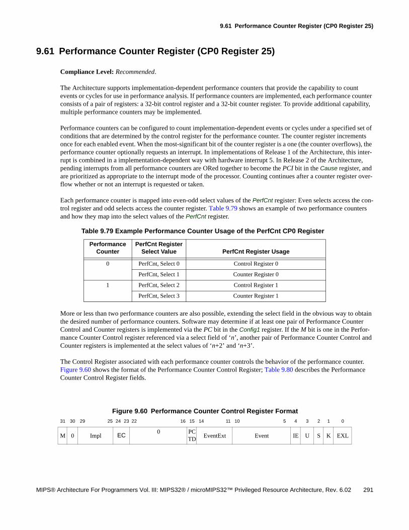
9.61 Performance Counter Register (CP0 Register 25)
MIPS® Architecture For Programmers Vol. III: MIPS32® / microMIPS32™ Privileged Resource Architecture, Rev. 6.02 291
9.61 Performance Counter Register (CP0 Register 25)
Compliance Level: Recommended.
The Architecture supports implementation-dependent performance counters that provide the capability to count events or cycles for use in performance analysis. If performance counters are implemented, each performance counter consists of a pair of registers: a 32-bit control register and a 32-bit counter register. To provide additional capability, multiple performance counters may be implemented.
Performance counters can be configured to count implementation-dependent events or cycles under a specified set of conditions that are determined by the control register for the performance counter. The counter register increments once for each enabled event. When the most-significant bit of the counter register is a one (the counter overflows), the performance counter optionally requests an interrupt. In implementations of Release 1 of the Architecture, this inter-rupt is combined in a implementation-dependent way with hardware interrupt 5. In Release 2 of the Architecture, pending interrupts from all performance counters are ORed together to become the PCI bit in the Cause register, and are prioritized as appropriate to the interrupt mode of the processor. Counting continues after a counter register over-flow whether or not an interrupt is requested or taken.
Each performance counter is mapped into even-odd select values of the PerfCnt register: Even selects access the con-trol register and odd selects access the counter register. Table 9.79 shows an example of two performance counters and how they map into the select values of the PerfCnt register.
More or less than two performance counters are also possible, extending the select field in the obvious way to obtain the desired number of performance counters. Software may determine if at least one pair of Performance Counter Control and Counter registers is implemented via the PC bit in the Config1 register. If the M bit is one in the Perfor-mance Counter Control register referenced via a select field of ‘n’, another pair of Performance Counter Control and Counter registers is implemented at the select values of ‘n+2’ and ‘n+3’.
The Control Register associated with each performance counter controls the behavior of the performance counter. Figure 9.60 shows the format of the Performance Counter Control Register; Table 9.80 describes the Performance Counter Control Register fields.
Table 9.79 Example Performance Counter Usage of the PerfCnt CP0 Register
Performance Counter
PerfCnt Register Select Value PerfCnt Register Usage
0 PerfCnt, Select 0 Control Register 0
PerfCnt, Select 1 Counter Register 0
1 PerfCnt, Select 2 Control Register 1
PerfCnt, Select 3 Counter Register 1
Figure 9.60 Performance Counter Control Register Format
31 30 29 25 24 23 22 16 15 14 11 10 5 4 3 2 1 0
M 0 Impl EC0 PC
TDEventExt Event IE U S K EXL
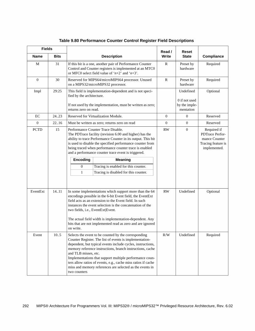
292 MIPS® Architecture For Programmers Vol. III: MIPS32® / microMIPS32™ Privileged Resource Architecture, Rev. 6.02
Table 9.80 Performance Counter Control Register Field Descriptions
Fields
DescriptionRead / Write
Reset State ComplianceName Bits
M 31 If this bit is a one, another pair of Performance Counter Control and Counter registers is implemented at an MTC0 or MFC0 select field value of ‘n+2’ and ‘n+3’.
R Preset by hardware
Required
0 30 Reserved for MIPS64/microMIPS64 processor. Unused on a MIPS32/microMIPS32 processor.
R Preset by hardware
Required
Impl 29:25 This field is implementation-dependent and is not speci-fied by the architecture.
If not used by the implementation, must be written as zero; returns zero on read.
Undefined
0 if not used by the imple-
mentation
Optional
EC 24..23 Reserved for Virtualization Module. 0 0 Reserved
0 22..16 Must be written as zero; returns zero on read 0 0 Reserved
PCTD 15 Performance Counter Trace Disable.The PDTrace facility (revision 6.00 and higher) has the ability to trace Performance Counter in its output. This bit is used to disable the specified performance counter from being traced when performance counter trace is enabled and a performance counter trace event is triggered.
RW 0 Required if PDTrace Perfor-mance Counter
Tracing feature is implemented.
EventExt 14..11 In some implementations which support more than the 64 encodings possible in the 6-bit Event field, the EventExt field acts as an extension to the Event field. In such instances the event selection is the concatenation of the two fields, i.e., EventExt|Event.
The actual field width is implementation-dependent. Any bits that are not implemented read as zero and are ignored on write.
RW Undefined Optional
Event 10..5 Selects the event to be counted by the corresponding Counter Register. The list of events is implementation-dependent, but typical events include cycles, instructions, memory reference instructions, branch instructions, cache and TLB misses, etc.Implementations that support multiple performance coun-ters allow ratios of events, e.g., cache miss ratios if cache miss and memory references are selected as the events in two counters
R/W Undefined Required
Encoding Meaning
0 Tracing is enabled for this counter.
1 Tracing is disabled for this counter.
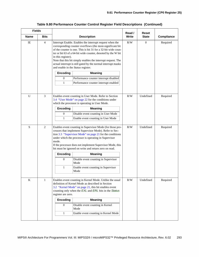
9.61 Performance Counter Register (CP0 Register 25)
MIPS® Architecture For Programmers Vol. III: MIPS32® / microMIPS32™ Privileged Resource Architecture, Rev. 6.02 293
IE 4 Interrupt Enable. Enables the interrupt request when the corresponding counter overflows (the most-significant bit of the counter is one. This is bit 31 for a 32-bit wide coun-ter or bit 63 of a 64-bit wide counter, denoted by the W bit in this register).Note that this bit simply enables the interrupt request. The actual interrupt is still gated by the normal interrupt masks and enable in the Status register.
R/W 0 Required
U 3 Enables event counting in User Mode. Refer to Section 3.4 “User Mode” on page 22 for the conditions under which the processor is operating in User Mode.
R/W Undefined Required
S 2 Enables event counting in Supervisor Mode (for those pro-cessors that implement Supervisor Mode). Refer to Sec-tion 3.3 “Supervisor Mode” on page 21 for the conditions under which the processor is operating in Supervisor mode.If the processor does not implement Supervisor Mode, this bit must be ignored on write and return zero on read.
R/W Undefined Required
K 1 Enables event counting in Kernel Mode. Unlike the usual definition of Kernel Mode as described in Section 3.2 “Kernel Mode” on page 21, this bit enables event counting only when the EXL and ERL bits in the Status register are zero.
R/W Undefined Required
Table 9.80 Performance Counter Control Register Field Descriptions (Continued)
Fields
DescriptionRead / Write
Reset State ComplianceName Bits
Encoding Meaning
0 Performance counter interrupt disabled
1 Performance counter interrupt enabled
Encoding Meaning
0 Disable event counting in User Mode
1 Enable event counting in User Mode
Encoding Meaning
0 Disable event counting in Supervisor Mode
1 Enable event counting in Supervisor Mode
Encoding Meaning
0 Disable event counting in Kernel Mode
1 Enable event counting in Kernel Mode
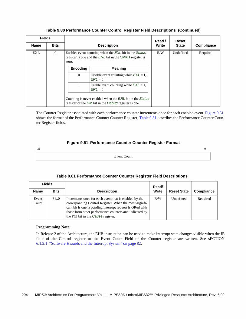
294 MIPS® Architecture For Programmers Vol. III: MIPS32® / microMIPS32™ Privileged Resource Architecture, Rev. 6.02
The Counter Register associated with each performance counter increments once for each enabled event. Figure 9.61 shows the format of the Performance Counter Counter Register; Table 9.81 describes the Performance Counter Coun-ter Register fields.
Programming Note:
In Release 2 of the Architecture, the EHB instruction can be used to make interrupt state changes visible when the IEfield of the Control register or the Event Count Field of the Counter register are written. See sECTION6.1.2.1 “Software Hazards and the Interrupt System” on page 82.
EXL 0 Enables event counting when the EXL bit in the Status register is one and the ERL bit in the Status register is zero.
Counting is never enabled when the ERL bit in the Status register or the DM bit in the Debug register is one.
R/W Undefined Required
Figure 9.61 Performance Counter Counter Register Format
31 0
Event Count
Table 9.81 Performance Counter Counter Register Field Descriptions
Fields
DescriptionRead/Write Reset State ComplianceName Bits
Event Count
31..0 Increments once for each event that is enabled by the corresponding Control Register. When the most-signifi-cant bit is one, a pending interrupt request is ORed with those from other performance counters and indicated by the PCI bit in the Cause register.
R/W Undefined Required
Table 9.80 Performance Counter Control Register Field Descriptions (Continued)
Fields
DescriptionRead / Write
Reset State ComplianceName Bits
Encoding Meaning
0 Disable event counting while EXL = 1, ERL = 0
1 Enable event counting while EXL = 1, ERL = 0
9.62 ErrCtl Register (CP0 Register 26, Select 0)
MIPS® Architecture For Programmers Vol. III: MIPS32® / microMIPS32™ Privileged Resource Architecture, Rev. 6.02 295
9.62 ErrCtl Register (CP0 Register 26, Select 0)
Compliance Level: Optional.
The ErrCtl register provides an implementation-dependent diagnostic interface with the error detection mechanisms implemented by the processor. This register has been used in previous implementations to read and write parity or ECC information to and from the primary or secondary cache data arrays in conjunction with specific encodings of the Cache instruction or other implementation-dependent method. The exact format of the ErrCtl register is imple-mentation-dependent and not specified by the architecture. Refer to the processor specification for the format of this register and a description of the fields.

296 MIPS® Architecture For Programmers Vol. III: MIPS32® / microMIPS32™ Privileged Resource Architecture, Rev. 6.02
9.63 CacheErr Register (CP0 Register 27, Select 0)
MIPS® Architecture For Programmers Vol. III: MIPS32® / microMIPS32™ Privileged Resource Architecture, Rev. 6.02 297
9.63 CacheErr Register (CP0 Register 27, Select 0)
Compliance Level: Optional.
The CacheErr register provides an interface with the cache error detection logic that may be implemented by a pro-cessor.
The exact format of the CacheErr register is implementation-dependent and not specified by the architecture. Refer to the processor specification for the format of this register and a description of the fields.

298 MIPS® Architecture For Programmers Vol. III: MIPS32® / microMIPS32™ Privileged Resource Architecture, Rev. 6.02
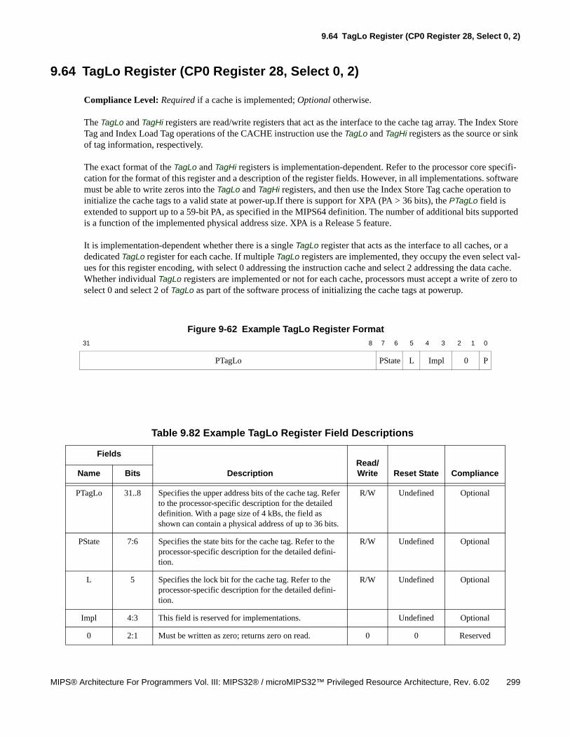
9.64 TagLo Register (CP0 Register 28, Select 0, 2)
MIPS® Architecture For Programmers Vol. III: MIPS32® / microMIPS32™ Privileged Resource Architecture, Rev. 6.02 299
9.64 TagLo Register (CP0 Register 28, Select 0, 2)
Compliance Level: Required if a cache is implemented; Optional otherwise.
The TagLo and TagHi registers are read/write registers that act as the interface to the cache tag array. The Index Store Tag and Index Load Tag operations of the CACHE instruction use the TagLo and TagHi registers as the source or sink of tag information, respectively.
The exact format of the TagLo and TagHi registers is implementation-dependent. Refer to the processor core specifi-cation for the format of this register and a description of the register fields. However, in all implementations. software must be able to write zeros into the TagLo and TagHi registers, and then use the Index Store Tag cache operation to initialize the cache tags to a valid state at power-up.If there is support for XPA (PA > 36 bits), the PTagLo field is extended to support up to a 59-bit PA, as specified in the MIPS64 definition. The number of additional bits supported is a function of the implemented physical address size. XPA is a Release 5 feature.
It is implementation-dependent whether there is a single TagLo register that acts as the interface to all caches, or a dedicated TagLo register for each cache. If multiple TagLo registers are implemented, they occupy the even select val-ues for this register encoding, with select 0 addressing the instruction cache and select 2 addressing the data cache. Whether individual TagLo registers are implemented or not for each cache, processors must accept a write of zero to select 0 and select 2 of TagLo as part of the software process of initializing the cache tags at powerup.
Figure 9-62 Example TagLo Register Format
31 8 7 6 5 4 3 2 1 0
PTagLo PState L Impl 0 P
Table 9.82 Example TagLo Register Field Descriptions
Fields
DescriptionRead/Write Reset State ComplianceName Bits
PTagLo 31..8 Specifies the upper address bits of the cache tag. Refer to the processor-specific description for the detailed definition. With a page size of 4 kBs, the field as shown can contain a physical address of up to 36 bits.
R/W Undefined Optional
PState 7:6 Specifies the state bits for the cache tag. Refer to the processor-specific description for the detailed defini-tion.
R/W Undefined Optional
L 5 Specifies the lock bit for the cache tag. Refer to the processor-specific description for the detailed defini-tion.
R/W Undefined Optional
Impl 4:3 This field is reserved for implementations. Undefined Optional
0 2:1 Must be written as zero; returns zero on read. 0 0 Reserved
300 MIPS® Architecture For Programmers Vol. III: MIPS32® / microMIPS32™ Privileged Resource Architecture, Rev. 6.02
P 0 Specifies the parity bit for the cache tag. Refer to the processor-specific description for the detailed defini-tion.
R/W Undefined Optional
Table 9.82 Example TagLo Register Field Descriptions (Continued)
Fields
DescriptionRead/Write Reset State ComplianceName Bits
9.65 DataLo Register (CP0 Register 28, Select 1, 3)
MIPS® Architecture For Programmers Vol. III: MIPS32® / microMIPS32™ Privileged Resource Architecture, Rev. 6.02 301
9.65 DataLo Register (CP0 Register 28, Select 1, 3)
Compliance Level: Optional.
The DataLo and DataHi registers are registers that act as the interface to the cache data array and are intended for diagnostic operation only. The Index Load Tag operation of the CACHE instruction reads the corresponding data val-ues into the DataLo and DataHi registers.
The exact format and operation of the DataLo and DataHi registers is implementation-dependent. Refer to the proces-sor specification for the format of this register and a description of the fields.
It is implementation-dependent whether there is a single DataLo register that acts as the interface to all caches, or a dedicated DataLo register for each cache. If multiple DataLo registers are implemented, they occupy the odd select values for this register encoding, with select 1 addressing the instruction cache and select 3 addressing the data cache.

302 MIPS® Architecture For Programmers Vol. III: MIPS32® / microMIPS32™ Privileged Resource Architecture, Rev. 6.02
9.66 TagHi Register (CP0 Register 29, Select 0, 2)
MIPS® Architecture For Programmers Vol. III: MIPS32® / microMIPS32™ Privileged Resource Architecture, Rev. 6.02 303
9.66 TagHi Register (CP0 Register 29, Select 0, 2)
Compliance Level: Required if a cache is implemented; Optional otherwise.
The TagLo and TagHi registers are read/write registers that act as the interface to the cache tag array. The Index Store Tag and Index Load Tag operations of the CACHE instruction use the TagLo and TagHi registers as the source or sink of tag information, respectively.
The exact format of the TagLo and TagHi registers is implementation-dependent. Refer to the processor specification for the format of this register and a description of the fields. However, software must be able to write zeros into the TagLo and TagHi registers and the use the Index Store Tag cache operation to initialize the cache tags to a valid state at powerup.
It is implementation-dependent whether there is a single TagHi register that acts as the interface to all caches, or a dedicated TagHi register for each cache. If multiple TagHi registers are implemented, they occupy the even select val-ues for this register encoding, with select 0 addressing the instruction cache and select 2 addressing the data cache. Whether individual TagHi registers are implemented or not for each cache, processors must accept a write of zero to select 0 and select 2 of TagHi as part of the software process of initializing the cache tags at powerup.

304 MIPS® Architecture For Programmers Vol. III: MIPS32® / microMIPS32™ Privileged Resource Architecture, Rev. 6.02
9.67 DataHi Register (CP0 Register 29, Select 1, 3)
MIPS® Architecture For Programmers Vol. III: MIPS32® / microMIPS32™ Privileged Resource Architecture, Rev. 6.02 305
9.67 DataHi Register (CP0 Register 29, Select 1, 3)
Compliance Level: Optional.
The DataLo and DataHi registers are registers that act as the interface to the cache data array and are intended for diagnostic operation only. The Index Load Tag operation of the CACHE instruction reads the corresponding data val-ues into the DataLo and DataHi registers.
The exact format and operation of the DataLo and DataHi registers is implementation-dependent. Refer to the proces-sor specification for the format of this register and a description of the fields.

306 MIPS® Architecture For Programmers Vol. III: MIPS32® / microMIPS32™ Privileged Resource Architecture, Rev. 6.02
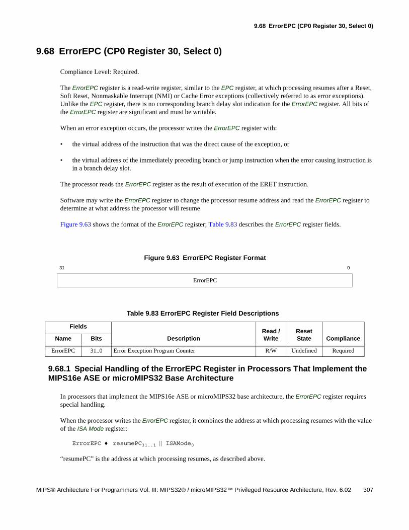
9.68 ErrorEPC (CP0 Register 30, Select 0)
MIPS® Architecture For Programmers Vol. III: MIPS32® / microMIPS32™ Privileged Resource Architecture, Rev. 6.02 307
9.68 ErrorEPC (CP0 Register 30, Select 0)
Compliance Level: Required.
The ErrorEPC register is a read-write register, similar to the EPC register, at which processing resumes after a Reset, Soft Reset, Nonmaskable Interrupt (NMI) or Cache Error exceptions (collectively referred to as error exceptions). Unlike the EPC register, there is no corresponding branch delay slot indication for the ErrorEPC register. All bits of the ErrorEPC register are significant and must be writable.
When an error exception occurs, the processor writes the ErrorEPC register with:
• the virtual address of the instruction that was the direct cause of the exception, or
• the virtual address of the immediately preceding branch or jump instruction when the error causing instruction is in a branch delay slot.
The processor reads the ErrorEPC register as the result of execution of the ERET instruction.
Software may write the ErrorEPC register to change the processor resume address and read the ErrorEPC register to determine at what address the processor will resume
Figure 9.63 shows the format of the ErrorEPC register; Table 9.83 describes the ErrorEPC register fields.
9.68.1 Special Handling of the ErrorEPC Register in Processors That Implement the MIPS16e ASE or microMIPS32 Base Architecture
In processors that implement the MIPS16e ASE or microMIPS32 base architecture, the ErrorEPC register requires special handling.
When the processor writes the ErrorEPC register, it combines the address at which processing resumes with the value of the ISA Mode register:
ErrorEPC resumePC31..1 ISAMode0
“resumePC” is the address at which processing resumes, as described above.
Figure 9.63 ErrorEPC Register Format
31 0
ErrorEPC
Table 9.83 ErrorEPC Register Field Descriptions
Fields
DescriptionRead / Write
Reset State ComplianceName Bits
ErrorEPC 31..0 Error Exception Program Counter R/W Undefined Required
308 MIPS® Architecture For Programmers Vol. III: MIPS32® / microMIPS32™ Privileged Resource Architecture, Rev. 6.02
When the processor reads the ErrorEPC register, it distributes the bits to the PC and ISAMode registers:
PC ErrorEPC31..1 0ISAMode ErrorEPC0
Software reads of the ErrorEPC register simply return to a GPR the last value written with no interpretation. Software writes to the ErrorEPC register store a new value which is interpreted by the processor as described above.
9.69 DESAVE Register (CP0 Register 31)
MIPS® Architecture For Programmers Vol. III: MIPS32® / microMIPS32™ Privileged Resource Architecture, Rev. 6.02 309
9.69 DESAVE Register (CP0 Register 31)
Compliance Level: Optional.
The DESAVE register is part of the EJTAG specification. Refer to that specification for the format and description of this register.
The DESAVE register is meant to be used solely while in Debug Mode. If kernel mode software uses this register, it would conflict with debugging kernel mode software. For that reason, it is strongly recommended that kernel mode software not use this register. If the KScratch* registers are implemented, kernel software can use those registers. (For Release 6, the KScratch* registers are mandatory.)

310 MIPS® Architecture For Programmers Vol. III: MIPS32® / microMIPS32™ Privileged Resource Architecture, Rev. 6.02
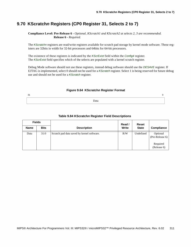
9.70 KScratchn Registers (CP0 Register 31, Selects 2 to 7)
MIPS® Architecture For Programmers Vol. III: MIPS32® / microMIPS32™ Privileged Resource Architecture, Rev. 6.02 311
9.70 KScratchn Registers (CP0 Register 31, Selects 2 to 7)
Compliance Level: Pre-Release 6 - Optional, KScratch1 and KScratch2 at selects 2, 3 are recommended. Release 6 - Required.
The KScratchn registers are read/write registers available for scratch pad storage by kernel mode software. These reg-isters are 32bits in width for 32-bit processors and 64bits for 64-bit processors.
The existence of these registers is indicated by the KScrExist field within the Config4 register. The KScrExist field specifies which of the selects are populated with a kernel scratch register.
Debug Mode software should not use these registers, instead debug software should use the DESAVE register. If EJTAG is implemented, select 0 should not be used for a KScratch register. Select 1 is being reserved for future debug use and should not be used for a KScratch register.
Figure 9.64 KScratchn Register Format
31 0
Data
Table 9.84 KScratchn Register Field Descriptions
Fields
DescriptionRead / Write
Reset State ComplianceName Bits
Data 31:0 Scratch pad data saved by kernel software. R/W Undefined Optional(Pre-Release 6)
Required(Release 6)

312 MIPS® Architecture For Programmers Vol. III: MIPS32® / microMIPS32™ Privileged Resource Architecture, Rev. 6.02
Appendix A
MIPS® Architecture For Programmers Vol. III: MIPS32® / microMIPS32™ Privileged Resource Architecture, Rev. 6.02 313
Alternative MMU Organizations
The main body of this specification describes the TLB-based MMU organization. This appendix describes other potential MMU organizations.
A.1 Fixed Mapping MMU
As an alternative to the full TLB-based MMU, the MIPS32/microMIPS32 Architecture supports a lightweight mem-ory management mechanism with fixed virtual-to-physical address translation, and no memory protection beyond what is provided by the address error checks required of all MMUs. This may be useful for those applications which do not require the capabilities of a full TLB-based MMU.
A.1.1 Fixed Address Translation
Address translation using the Fixed Mapping MMU is done as follows:
• Kseg0 and Kseg1 addresses are translated in an identical manner to the TLB-based MMU: they both map to the low 512MB of physical memory.
• Useg/Suseg/Kuseg addresses are mapped by adding 1GB to the virtual address when the ERL bit is zero in the Status register, and are mapped using an identity mapping when the ERL bit is one in the Status register.
• Sseg/Ksseg/Kseg2/Kseg3 addresses are mapped using an identity mapping.
Supervisor Mode is not supported with a Fixed Mapping MMU.
Table A.1 lists all mappings from virtual to physical addresses. Note that address error checking is still done before the translation process. Therefore, an attempt to reference kseg0 from User Mode still results in an address error exception, just as it does with a TLB-based MMU.
Table A.1 Physical Address Generation from Virtual Addresses
Segment Name Virtual Address
Generates Physical Address
StatusERL = 0 StatusERL = 1
usegsusegkuseg
0x0000 0000through
0x7FFF FFFF
0x4000 0000through
0xBFFF FFFF
0x0000 0000through
0x7FFF FFFF
kseg0 0x8000 0000through
0x9FFF FFFF
0x0000 0000through
0x1FFF FFFF
kseg10xA000 0000
through0xBFFF FFFF
0x0000 0000through
0x0x1FFF FFFF
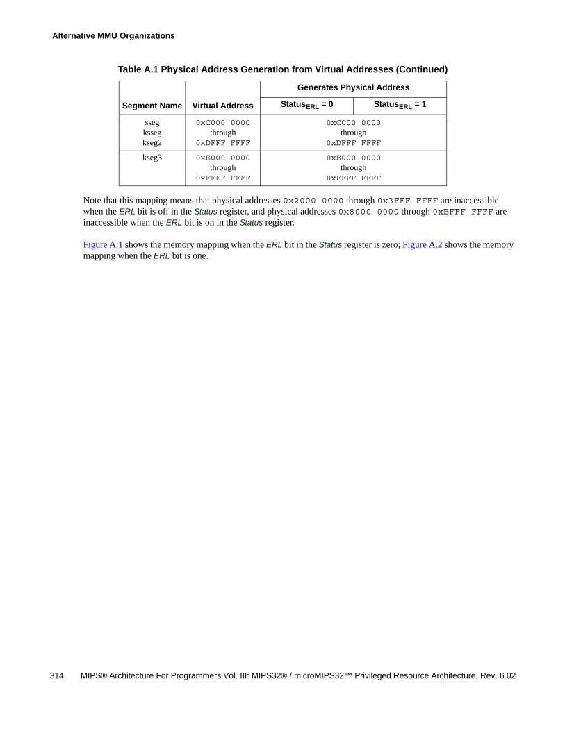
Alternative MMU Organizations
314 MIPS® Architecture For Programmers Vol. III: MIPS32® / microMIPS32™ Privileged Resource Architecture, Rev. 6.02
Note that this mapping means that physical addresses 0x2000 0000 through 0x3FFF FFFF are inaccessible when the ERL bit is off in the Status register, and physical addresses 0x8000 0000 through 0xBFFF FFFF are inaccessible when the ERL bit is on in the Status register.
Figure A.1 shows the memory mapping when the ERL bit in the Status register is zero; Figure A.2 shows the memory mapping when the ERL bit is one.
ssegkssegkseg2
0xC000 0000through
0xDFFF FFFF
0xC000 0000through
0xDFFF FFFF
kseg3 0xE000 0000through
0xFFFF FFFF
0xE000 0000through
0xFFFF FFFF
Table A.1 Physical Address Generation from Virtual Addresses (Continued)
Segment Name Virtual Address
Generates Physical Address
StatusERL = 0 StatusERL = 1
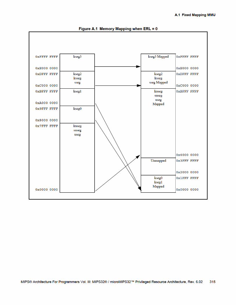
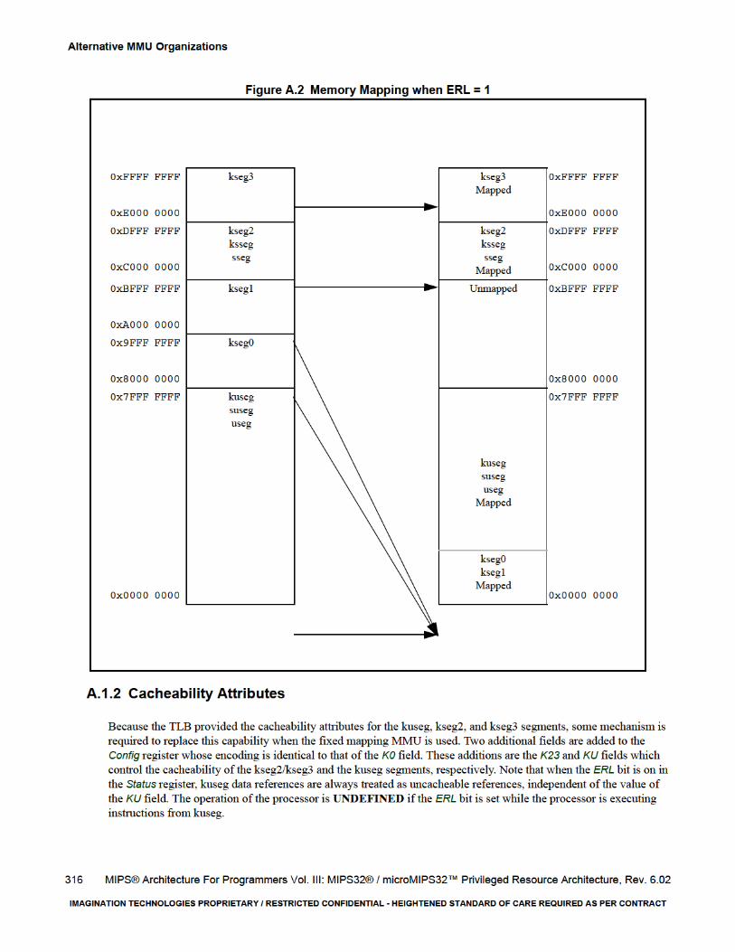
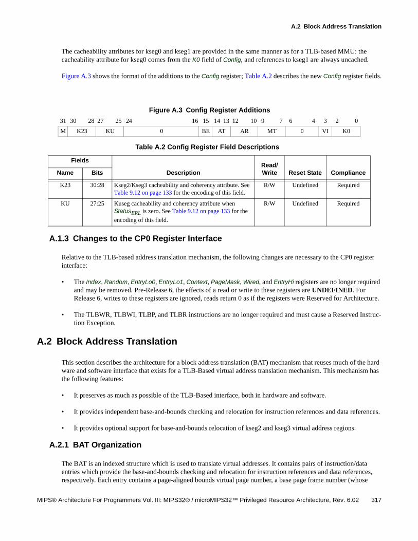
A.2 Block Address Translation
MIPS® Architecture For Programmers Vol. III: MIPS32® / microMIPS32™ Privileged Resource Architecture, Rev. 6.02 317
The cacheability attributes for kseg0 and kseg1 are provided in the same manner as for a TLB-based MMU: the cacheability attribute for kseg0 comes from the K0 field of Config, and references to kseg1 are always uncached.
Figure A.3 shows the format of the additions to the Config register; Table A.2 describes the new Config register fields.
A.1.3 Changes to the CP0 Register Interface
Relative to the TLB-based address translation mechanism, the following changes are necessary to the CP0 register interface:
• The Index, Random, EntryLo0, EntryLo1, Context, PageMask, Wired, and EntryHi registers are no longer required and may be removed. Pre-Release 6, the effects of a read or write to these registers are UNDEFINED. For Release 6, writes to these registers are ignored, reads return 0 as if the registers were Reserved for Architecture.
• The TLBWR, TLBWI, TLBP, and TLBR instructions are no longer required and must cause a Reserved Instruc-tion Exception.
A.2 Block Address Translation
This section describes the architecture for a block address translation (BAT) mechanism that reuses much of the hard-ware and software interface that exists for a TLB-Based virtual address translation mechanism. This mechanism has the following features:
• It preserves as much as possible of the TLB-Based interface, both in hardware and software.
• It provides independent base-and-bounds checking and relocation for instruction references and data references.
• It provides optional support for base-and-bounds relocation of kseg2 and kseg3 virtual address regions.
A.2.1 BAT Organization
The BAT is an indexed structure which is used to translate virtual addresses. It contains pairs of instruction/data entries which provide the base-and-bounds checking and relocation for instruction references and data references, respectively. Each entry contains a page-aligned bounds virtual page number, a base page frame number (whose
Figure A.3 Config Register Additions
31 30 28 27 25 24 16 15 14 13 12 10 9 7 6 4 3 2 0
M K23 KU 0 BE AT AR MT 0 VI K0
Table A.2 Config Register Field Descriptions
Fields
DescriptionRead/Write Reset State ComplianceName Bits
K23 30:28 Kseg2/Kseg3 cacheability and coherency attribute. See Table 9.12 on page 133 for the encoding of this field.
R/W Undefined Required
KU 27:25 Kuseg cacheability and coherency attribute when StatusERL is zero. See Table 9.12 on page 133 for the
encoding of this field.
R/W Undefined Required
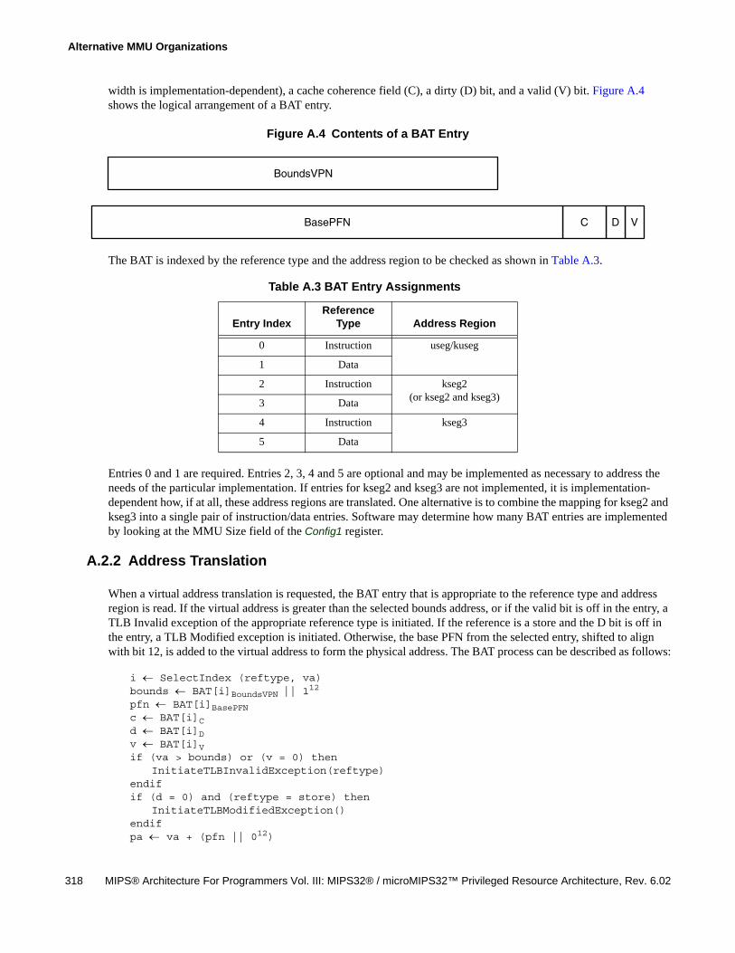
Alternative MMU Organizations
318 MIPS® Architecture For Programmers Vol. III: MIPS32® / microMIPS32™ Privileged Resource Architecture, Rev. 6.02
width is implementation-dependent), a cache coherence field (C), a dirty (D) bit, and a valid (V) bit. Figure A.4 shows the logical arrangement of a BAT entry.
Figure A.4 Contents of a BAT Entry
The BAT is indexed by the reference type and the address region to be checked as shown in Table A.3.
Entries 0 and 1 are required. Entries 2, 3, 4 and 5 are optional and may be implemented as necessary to address the needs of the particular implementation. If entries for kseg2 and kseg3 are not implemented, it is implementation-dependent how, if at all, these address regions are translated. One alternative is to combine the mapping for kseg2 and kseg3 into a single pair of instruction/data entries. Software may determine how many BAT entries are implemented by looking at the MMU Size field of the Config1 register.
A.2.2 Address Translation
When a virtual address translation is requested, the BAT entry that is appropriate to the reference type and address region is read. If the virtual address is greater than the selected bounds address, or if the valid bit is off in the entry, a TLB Invalid exception of the appropriate reference type is initiated. If the reference is a store and the D bit is off in the entry, a TLB Modified exception is initiated. Otherwise, the base PFN from the selected entry, shifted to align with bit 12, is added to the virtual address to form the physical address. The BAT process can be described as follows:
i SelectIndex (reftype, va)bounds BAT[i]BoundsVPN || 1
12
pfn BAT[i]BasePFNc BAT[i]Cd BAT[i]Dv BAT[i]Vif (va > bounds) or (v = 0) then
InitiateTLBInvalidException(reftype)endifif (d = 0) and (reftype = store) then
InitiateTLBModifiedException()endifpa va + (pfn || 012)
Table A.3 BAT Entry Assignments
Entry IndexReference
Type Address Region
0 Instruction useg/kuseg
1 Data
2 Instruction kseg2(or kseg2 and kseg3)3 Data
4 Instruction kseg3
5 Data
VDCBasePFN
BoundsVPN
A.3 Dual Variable-Page-Size and Fixed-Page-Size TLBs
MIPS® Architecture For Programmers Vol. III: MIPS32® / microMIPS32™ Privileged Resource Architecture, Rev. 6.02 319
Making all addresses out-of-bounds can only be done by clearing the valid bit in the BAT entry. Setting the bounds value to zero leaves the first virtual page mapped.
A.2.3 Changes to the CP0 Register Interface
Relative to the TLB-based address translation mechanism, the following changes are necessary to the CP0 register interface:
• The Index register is used to index the BAT entry to be read or written by the TLBWI and TLBR instructions.
• The EntryHi register is the interface to the BoundsVPN field in the BAT entry.
• The EntryLo0 register is the interface to the BasePFN and C, D, and V fields of the BAT entry. The register has the same format as for a TLB-based MMU.
• The Random, EntryLo1, Context, PageMask, and Wired registers are eliminated. Pre-Release 6 the effects of a read or write to these registers are UNDEFINED. For Release 6, writes to these registers are ignored, reads return 0 as if the registers were Reserved for Architecture.
• The TLBP and TLBWR instructions are unnecessary. The TLBWI and TLBR instructions reference the BAT entry whose index is contained in the Index register. The effects of executing a TLBP or TLBWR are UNDE-FINED, but processors should signal a Reserved Instruction Exception.
A.3 Dual Variable-Page-Size and Fixed-Page-Size TLBs
Most MIPS CPU cores implement a fully associative Joint TLB. Unfortunately, such fully-associative structures can be slow, can require a large amount of logic components to implement and can dissipate a lot of power. The number of entries for a fully associative array that can be practically implemented is not large.
In high performance systems, it is desirable to minimize the frequency of TLB misses. In small and low-cost systems, it is desirable to keep the implementation costs of a TLB to a minimum. This section describes an optional alternative MMU configuration which decreases the implementation costs of a small TLB as well as allows for a TLB that can map a very large number of pages to be reasonably implemented.
A.3.1 MMU Organization
This alternative MMU configuration uses two TLB structures.
1. This first TLB is called the Fixed-Page-Size TLB or the FTLB.
• At any one time, all entries within the FTLB use a shared, common page size.
• The FTLB is not fully-associative, but rather set associative.
• The number of ways per set is implementation specific.
• The number of sets is implementation specific.
• The common page size is also implementation specific.
Alternative MMU Organizations
320 MIPS® Architecture For Programmers Vol. III: MIPS32® / microMIPS32™ Privileged Resource Architecture, Rev. 6.02
• The common page size is allowed to be software configurable. The choice of the common page size is done once for the entire FTLB, not on a per-entry basis. This configuration by software can only be done after a full flush/initialization of the FTLB, before there are any valid entries within the FTLB. Implementations are also allowed to support only one page size for the FTLB - in that case, the FTLB page size is fixed by hard-ware and not software configurable.
• The EHINV TLB invalidate feature is required for FTLB implementation. The legacy method of using reserved address values to represent invalid TLB entries is not guaranteed to work where the implementation can limit what addresses are allowable at a specific TLB index.
2. The second TLB is called the Variable-Page-Size TLB or the VTLB.
• The choice of page size is done on a per-entry basis. That is, one VTLB entry can use a page size that is dif-ferent from the size used by another VTLB entry.
• The VTLB is fully-associative.
• The number of entries is implementation specific.
• The set of allowable page sizes for VTLB entries is implementation specific.
Just as for the JTLB, both the FTLB and VTLB are shared between the instruction stream and the data stream. For address translation, the virtual address is presented to both the FTLB and VTLB in parallel. Entries in both structures are accessed in parallel to search for the physical address.
The use of two TLB structures has these benefits:
• The implementation costs of building a set-associative TLB with many entries can be much less than that of implementing a large fully-associative TLB.
• The existence of a VTLB retains the capability of using large pages to map large sections of physical memory without consuming a large number of entries in the FTLB.
Random replacement of pages in the MMU happens mainly in the FTLB. In most operating systems, on-demand pag-ing only uses one page size so the FTLB is sufficient for this purpose. Some of the address bits of the specified virtual address are used to index into the FTLB as appropriate for the chosen FTLB array size. The method of choosing which FTLB way to modify is implementation specific.
The VTLB is very similar to the JTLB. The C0_PageMask register is used to program the page size used for a partic-ular VTLB entry.
The configuration of the FTLB is reflected in the FTLB fields within the new Config4 register. The size of the VTLB is reflected in the Config1MMUSize-1 field. The presence of the dual FTLB and VTLB is denoted by the value of 0x4 in
ConfigMT register field. These registers are described in “Changes to the COP0 Registers” on page 323.
Most implementations would choose to build a VTLB with a smaller number of entries and a FTLB with a larger number of entries. This combination allows for many on-demand fixed-sized pages as well as for a small number of large address blocks to be simultaneously mapped by the MMU.
A.3 Dual Variable-Page-Size and Fixed-Page-Size TLBs
MIPS® Architecture For Programmers Vol. III: MIPS32® / microMIPS32™ Privileged Resource Architecture, Rev. 6.02 321
A.3.2 Programming Interface
The software programming interface used for the fully-associative JTLB is maintained as much as possible to decrease the amount of software porting.
Also for that purpose, each entry in the FTLB as well as the VTLB use one tag (VPN2) to map two physical pages (PFN), just as in the JTLB. The entries in either array are accessed through the C0_EntryHi and C0_EntryLo0/1 regis-ters.
Entries in either array (FTLB or VTLB) can be accessed with the TLBWI and TLBWR instructions.
The PageMask register is used to set the page size for the VTLB entries. This register is also used to choose which array (FTLB or VTLB) to write for the TLBWR instruction.
For the rest of this section, the following parameters are used:
3. FPageSize - the page size used by the FTLB entries
4. FSetSize - Number of entries in one way of the FTLB.
5. FWays - Number of ways within a set of the FTLB.
6. VIndex - Number of entries in the VTLB.
For the C0_Index, the C0_Wired registers, the TLBP, TLBR and TLBWI instructions; the VTLB occupies indices 0 to VIndex-1. The FTLB occupies indices VIndex to VIndex + (FSetSize * FWays)-1.
The TLBP instruction produces a value which can be used by the TLBWI instruction without modification by soft-ware. When referring to the FTLB, the value is the concatenation of the selected FTLB way and set, and incremented by the size of the VTLB. For example, {selected FTLB Way, selected FTLB Set} + VIndex.
If C0_PageMask is set to the page size used by the FTLB, the TLBWR instruction modifies entries within the FTLB or the VTLB. It is implementation specific whether the VTLB will be modified for this case.
How the FTLB set-associative array is indexed is implementation specific. In any indexing scheme, the least signifi-cant address bit that can be used for indexing is log2(FPageSize)+1. The number of index bits needed to select the
correct set within the FTLB array is log2(FSetSize).
Since the FTLB array can be modified through the TLBWI instruction, it is possible for software to choose an inap-propriate FTLB index value for the specified virtual address. In this case, it is implementation specific whether a Machine Check exception is generated for the TLBWI instruction.
The EHINV TLB entry invalidate feature is required for a FTLB. Since it is implementation defined as to whether a particular FTLB index value can be used for a specific virtual address, the legacy method of representing an invalid TLB entry by using a predefined address value is not guaranteed to work.
The method of choosing which FTLB way to modify is implementation specific.
If C0_PageMask is not set to the page size used by the FTLB, the TLBWR instruction modifies entries within the VTLB. The VTLB entry to be written is specified by the log2(VIndex) least significant bits of the C0_Random regis-
ter value.
Alternative MMU Organizations
322 MIPS® Architecture For Programmers Vol. III: MIPS32® / microMIPS32™ Privileged Resource Architecture, Rev. 6.02
For both the TLBWR and TLBWI instruction, it is implementation specific whether both (FTLB and VTLB) arrays are checked for duplicate or overlapping entries and whether a Machine Check exception is generated for these cases.
A.3.2.1 Example with chosen FTLB and VTLB sizes
As an example, let’s assume an implementation chooses these values:
1. FPageSize - 4 kB used by the FTLB entries
2. FSetSize - 128 in one way of the FTLB.
3. FWays - 4 ways within a set of the FTLB. (The FTLB has (128 sets x 4 ways/set) 512 entries, capable of map-ping (512 entries x 2 pages/entry x 4 kB/page) 4MB of address space simultaneously.
4. VIndex - 8 entries in the VTLB.
For the C0_Index, the C0_Wired registers, the TLBP, TLBR and TLBWI instructions; the VTLB occupies indices 0 to 7. The FTLB occupies indices 8 to 519.
The FTLB entries have a VPN2 field which starts at virtual address bit 12.
The least significant virtual address bit that can be used for FTLB indexing is virtual address 13. To index the FTLB set-associative array, 7 index bits are needed.
In this simple example, the design uses contiguous virtual address bits directly for indexing the FTLB (it does not cre-ate a hash for the FTLB indexing). The FTLB set-associative array is indexed using virtual address bits 19:13. The TLBWR instruction uses these address bits held in C0_EntryHi.
In this simple example, the design uses a cycle counter of 2 bits for way selection within the FTLB.
The Random register field within C0_Random is 3 bits wide to select the entry within the VTLB.
A.3.3 Changes to the TLB Instructions
TLBP
Both the VTLB and the FTLB are probed in parallel for the specified virtual address.
If the address hits in the VTLB, C0_Index specifies the entry within the VTLB (a value within 0 to VIndex-1).
If the address hits in the FTLB, C0_Index specifies the entry within the FTLB (a value within VIndex to VIn-dex+(FSetSize * FWays)-1). Which bits are used to encode the selected FTLB set as opposed to which bits are used to encode the selected FTLB way is implementation specific, but must match what is expected by the TLBWI instruction implementation. C0_PageMask reflects the page size used by the FTLB.
TLBR
Either a VTLB entry or a FTLB entry is read depending on the specified index in C0_Index.
Index values of 0 to VIndex-1 access the VTLB. Index values VIndex to VIndex+(FSetSize * FWays)-1 access the FTLB.
TLBWI

A.3 Dual Variable-Page-Size and Fixed-Page-Size TLBs
MIPS® Architecture For Programmers Vol. III: MIPS32® / microMIPS32™ Privileged Resource Architecture, Rev. 6.02 323
Either the VTLB or FTLB entry is written depending on the specified index in C0_Index.
Index values of 0 to VIndex-1 access the VTLB. Index values VIndex to VIndex+(FSetSize * FWays)-1 access the FTLB.
It is implementation specific if the hardware checks the VPN2 field of C0_EntryHi is appropriate for the specified set within the FTLB. The implementation may generate a machine-check exception if the VPN2 field is not appropriate for the specified set.
It is implementation-specific if the hardware checks both arrays (FTLB and VTLB) for valid duplicate or over-lapping entries and if the hardware signals a Machine Check exception for these cases.
TLBWR
Either the VTLB or FTLB entry is written depending on the specified page size in C0_PageMask.
If C0_PageMask is set to any page size other than that used by the FTLB, the TLBWR instruction modifies a VTLB entry. The VTLB entry is specified by the Random register field within C0_Random.
If C0_PageMask is set to the page size used by the FTLB, the TLBWR modifies either a FTLB entry or a VLTB entry. It is implementation specific which array is modified. The FTLB set-associative array is indexed in an implementation-specific manner.
The method of selecting which FTLB way to modify is implementation specific.
It is implementation specific if the hardware checks both arrays (FTLB and VTLB) for valid duplicate or over-lapping entries and if the hardware signals a Machine Check exception for these cases.
A.3.4 Changes to the COP0 Registers
C0_Config4 (CP0 Register 16, Select 4)
A new register introduced to reflect the FTLB configuration. Config4MMUExtDef register field must be set to a
value of 2 or 3 to reflect that the Dual VTLB and FTLB configuration is implemented. If either Config4 is not implemented or the Config4MMUExtDef field is not fixed to 2 or 3, the Dual VTLB/FTLB configuration is not
implemented.
If Config4MMUExtDef is fixed to a value of 2 or 3, the FTLBPageSize, FTLBWays and FTLBSets fields reflect the
FTLB configuration. Please refer to “Configuration Register 4 (CP0 Register 16, Select 4)” on page 253 for more detail on this register.
For Release 6, Config4MMUExtDef is reserved; see the description for the Config4 register.
C0_Config1 (CP0 Register 16, Select 1)
If Config4MMUExtDef is fixed to a value of 2 or 3, the MMUSize-1 register field is redefined to reflect only the size
of the VTLB.
C0_Config (CP0 Register 16, Select 0)
If ConfigMT is fixed to a value of 4, the implemented MMU Type is the dual FTLB and VTLB configuration.
Alternative MMU Organizations
324 MIPS® Architecture For Programmers Vol. III: MIPS32® / microMIPS32™ Privileged Resource Architecture, Rev. 6.02
C0_Index (CP0 Register 0, Select 0)
If Config4MMUExtDef is fixed to a value of 2 or 3, the register is redefined in this way:
The value held in the Index field can refer to either an entry in the FTLB or the VTLB. Index values of 0 to VIndex-1 access the VTLB. Index values VIndex to VIndex+(FSetSize * FWays)-1 access the FTLB. Which bits in the register field which encode the FTLB set as opposed to which bits encode the FTLB way is implementation specific, but must match what is expected by the TLBWI instruction implementation.
C0_Random (CP0 Register 1, Select 0)
For Release 6, this register has been deprecated.
If Config4MMUExtDef is fixed to a value of 2 or 3, the register is redefined in this way:
If the value in C0_PageMask is not set to the page-size used by the FTLB, and a TLBWR instruction is exe-cuted, a VTLB entry is modified. The Random register field is used to select the VTLB entry which is mod-ified.
If the value in C0_PageMask is set to the page-size used by the FTLB, and a TLBWR instruction is exe-cuted, a FTLB entry or a VTLB entry is modified. It is implementation specific whether the C0_RANDOM register is used to select the FTLB entry.
The upper bound of the Random register field value is VIndex.
C0_Wired (CP0 Register 6, Select 0)
If Config4MMUExtDef is fixed to a value of 2 or 3, the Wired register field can only hold a value of VIndex-1 or
less. That is, only VTLB entries can be wired down.
C0_PageMask (CP0 Register 5, Select 0)
If Config4MMUExtDef is fixed to a value of 2 or 3, the register is redefined in this way:
The Mask and MaskX field values determine whether the VTLB or the FTLB is modified by a TLBWR instruction.
The Mask and MaskX register fields do not affect the TLB address match operation for FTLB entries. The page size used by the FTLB entries are specified by the Config4FPageSize register field.
The software writeable bits in the Mask and MaskX fields reflect what page sizes are available in the VTLB. These fields do not reflect the page sizes which are available in the FTLB.
A.3.5 Software Compatibility
One of the main software visible changes introduced by this alternative MMU are the values reported in the C0_Index register. Previously, it was just a simple linear index. For this alternative MMU configuration, the value reflects both a selected way as well as a selected set when a FTLB entry is specified.
A.3 Dual Variable-Page-Size and Fixed-Page-Size TLBs
MIPS® Architecture For Programmers Vol. III: MIPS32® / microMIPS32™ Privileged Resource Architecture, Rev. 6.02 325
Fortunately, this Index value isn’t frequently generated by software nor read by software. Instead, the contents of the C0_Index register is generated by hardware upon a TLBP instruction. Software then just issues the TLBWI instruc-tion once the C0_EnLo* registers have been appropriately modified.
Another software visible change is that the MMUSize-1 field no longer reports the entire MMU size. For TLB initial-ization and TLB flushing, the contents of Config1MMUSize-1, Config4FTLBWays and Config4FTLBSets register fields must
all be read to calculate the entire number of TLB entries that must be initialized. TLB initialization and flushing are the only times software needs to generate an Index value to write into the C0_Index register.
Only the VTLB entries may be wired down. This limitation is due to using some of the EntryHi VPN2 bits to index the FTLB array.
If a page using the FTLB page-size is to be wired down, that page must be programmed into the VTLB using the TLBWI instruction, as the TLBWR instruction would only access the FTLB in that situation and could not access any wired-down TLB entry. The TLBWI instruction is normally used for wired-down pages, so this restriction should not affect existing software.
The EHINV TLB entry invalidate feature is required for a FTLB. Since it is implementation-defined as to whether a particular FTLB index value can be used for a specific virtual address, the legacy method of representing an invalid TLB entry by using a predefined address value is not guaranteed to work.
Alternative MMU Organizations
326 MIPS® Architecture For Programmers Vol. III: MIPS32® / microMIPS32™ Privileged Resource Architecture, Rev. 6.02
Appendix B
MIPS® Architecture For Programmers Vol. III: MIPS32® / microMIPS32™ Privileged Resource Architecture, Rev. 6.02 327
Revision History
Revision Date Description
0.92 January 20, 2001 Internal review copy of reorganized and updated architecture documentation.
0.95 March 12, 2001 Clean up document for external review release
1.00 August 29, 2002 Update based on review feedback:• Change ProbEn to ProbeTrap in the EJTAG Debug entry vector location discussion.• Add cache error and EJTAG Debug exceptions to the list of exceptions that do not go through
the general exception processing mechanism.• Fix incorrect branch offset adjustment in general exception processing pseudo code to deal
with extended MIPS16e instructions.• Add ConfigVI to denote an instruction cache with both virtual indexing and virtual tags.
• Correct XContext register description to note that both BadVPN2 and R fields are UNPRE-DICTABLE after an address error exception.
• Note that Supervisor Mode is not supported with a Fixed Mapping MMU.• Define TagLo bits 4..3 as implementation-dependent.• Describe the intended usage model differences between Reset and Soft Reset Exceptions.• Correct the minimum number of TLB entries to be 3, not 2, and show an example of the need
for 3.• Modify the description of PageMask and the TLB lookup process to acknowledge the fact
that not all implementations may support all page sizes.
1.90 September 1, 2002 Update the specification with the changes introduced in Release 2 of the Architecture. Changes in this revision include:• The following new Coprocessor 0 registers were added: EBase, HWREna, IntCtl, PageGrain,
SRSCtl, SRSMap.• The following Coprocessor 0 registers were modified: Cause, Config, Config2, Config3,
EntryHi, EntryLo0, EntryLo1, PageMask, PerfCnt, Status, WatchHi, WatchLo.• The descriptions of Virtual memory, exceptions, and hazards have been updated to reflect the
changes in Release 2.• A chapter on GPR shadow registers has been added.• The chapter on CP0 hazards has been completely rewritten to reflect the Release 2 changes.
Revision History
328 MIPS® Architecture For Programmers Vol. III: MIPS32® / microMIPS32™ Privileged Resource Architecture, Rev. 6.02
2.00 June 9, 2003 Complete the update to include Release 2 changes. These include:• Make bits 12..11 of the PageMask register power up zero and be gated by 1K page enable.
This eliminates the problem of having these bits set to 0b11 on a Release 2 chip in which ker-nel software has not enabled 1K page support.
• Correct the address of the cache error vector when the BEV bit is 1. It should be 0xBFC0.0300,. not 0xBFC0.0200.
• Correct the introduction to shadow registers to note that the SRSCtl register is not updated at the end of an exception in which StatusBEV = 1.
• Clarify that a MIPS16e PC-relative load reference is a data reference for the purposes of the Watch registers.
• Add note about a hardware interrupt being deasserted between the time that the processor detects the interrupt request and the time that the software interrupt handler runs. Software must be prepared for this case and simply dismiss the interrupt via an ERET.
• Add restriction that software must set EBase15 12 to zero in all bit positions less than or equal
to the most significant bit in the vector offset. This is only required in certain combinations of vector number and vector spacing when using VI or EIC Interrupt modes.
• Add suggested software TLB init routine which reduced the probability of triggering a machine check.
2.50 July 1, 2005 Changes in this revision:• Correct the encoding table description for the CausePCI bit to indicate that the bit controls
the performance counter, not the timer interrupt.• Correct the figure Interrupt Generation for External Interrupt Controller Interrupt Mode to
show CauseIP1 0 going to the EIC, rather than StatusIP1 0
• Update all files to FrameMaker 7.1.• Update reset exception list to reflect missing Release 2 reset requirements.• Define bits 31..30 in the HWREna register as access enables for the implementation-depen-
dent hardware registers 31 and 30.• Add definition for Coprocessor 0 Enable to Operating Modes chapter.• Add K23 and KU fields to main Config register definition as a pointer to the Fixed Mapping
MMU appendix.• Add specific note about the need to implement all shadow sets between 0 and HSS - no holes
are allowed.• Change the hazard from a software write to the SRSCtlPSS field and a RDPGPR and WRP-
GPR and instruction hazard vs. an execution hazard.• Correct the pseudo-code in the cache error exception description to reflect the Release 2
change that introduced EBase.• Document that EHB clears instruction state change hazards for writes to interrupt-related
fields in the Status, Cause, Compare, and PerfCnt registers.• Note that implementation-dependent bits in the Status and Config registers should be
defined in such a way that standard boot software will run, and that software which preserves the value of the field when writing the registers will also run correctly.
• With Release 2 of the Architecture the FR bit in the Status register should be a R/W bit, not a R bit.
• Improve the organization of the CP0 hazards table, and document that DERET, ERET, and exceptions and interrupts clear all hazards before the instruction fetch at the target instruction.
• Add list of MIPS® MT CP0 registers and MIPS MT and MIPS® DSP present bits in the Config3 register.
Revision Date Description
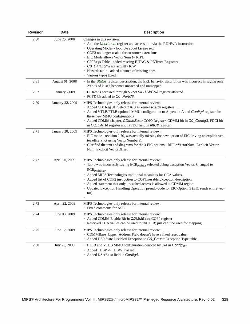
MIPS® Architecture For Programmers Vol. III: MIPS32® / microMIPS32™ Privileged Resource Architecture, Rev. 6.02 329
2.60 June 25, 2008 Changes in this revision:• Add the UserLocal register and access to it via the RDHWR instruction.• Operating Modes - footnote about ksseg/sseg• COP3 no longer usable for customer extensions• EIC Mode allows VectorNum != RIPL• CP0Regs Table - added missing EJTAG & PDTrace Registers• C0_DataLo/Hi are actually R/W• Hazards table - added a bunch of missing ones• Various typos fixed.
2.61 August 01, 2008 • In the Status register description, the ERL behavior description was incorrect in saying only 29 bits of kuseg becomes uncached and unmapped.
2.62 January 2,009 • CCRes is accessed through $3 not $4 - HWENA register affected. • PCTD bit added to C0_PerfCtl.
2.70 January 22, 2009 MIPS Technologies-only release for internal review:• Added CP0 Reg 31, Select 2 & 3 as kernel scratch registers.• Added VTLB/FTLB optional MMU configuration to Appendix A and Config4 register for
these new MMU configurations• Added CDMM chapter, CDMMBase COP0 Register, CDMM bit in C0_Config3, FDCI bit
in C0_Cause register and IPFDC field in IntCtl register.
2.71 January 28, 2009 MIPS Technologies-only release for internal review:• EIC mode - revision 2.70, was actually missing the new option of EIC driving an explicit vec-
tor offset (not using VectorNumbers). • Clarified the text and diagrams for the 3 EIC options - RIPL=VectorNum, Explicit Vector-
Num; Explicit VectorOffset.
2.72 April 20, 2009 MIPS Technologies-only release for internal review:• Table was incorrectly saying ECRProbEn selected debug exception Vector. Changed to
ECRProbTrap.
• Added MIPS Technologies traditional meanings for CCA values. • Added list of COP2 instruction to COPUnusable Exception description. • Added statement that only uncached access is allowed to CDMM region. • Updated Exception Handling Operation pseudo-code for EIC Option_3 (EIC sends entire vec-
tor).•
2.73 April 22, 2009 MIPS Technologies-only release for internal review:• Fixed comments for ASE.
2.74 June 03, 2009 MIPS Technologies-only release for internal review:• Added CDMM Enable Bit in CDMMBase COP0 register• Reserved CCA values can be used to init TLB; just can’t be used for mapping.
2.75 June 12, 2009 MIPS Technologies-only release for internal review:• CDMMBase_Upper_Address Field doesn’t have a fixed reset value. • Added DSP State Disabled Exception to C0_Cause Exception Type table.
2.80 July 20, 2009 • FTLB and VTLB MMU configuration denoted by 0x4 in ConfigMT
• Added TLBP -> TLBWI hazard• Added KScrExist field in Config4.
Revision Date Description
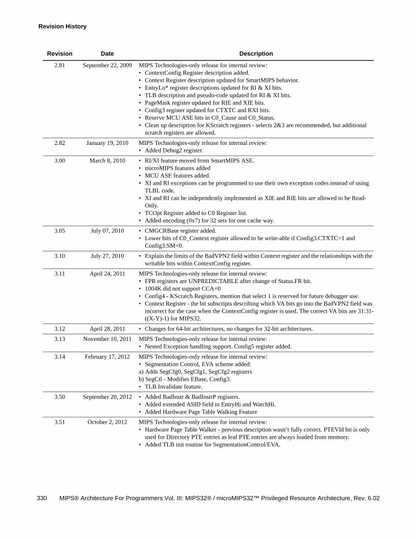
Revision History
330 MIPS® Architecture For Programmers Vol. III: MIPS32® / microMIPS32™ Privileged Resource Architecture, Rev. 6.02
2.81 September 22, 2009 MIPS Technologies-only release for internal review:• ContextConfig Register description added. • Context Register description updated for SmartMIPS behavior. • EntryLo* register descriptions updated for RI & XI bits. • TLB description and pseudo-code updated for RI & XI bits. • PageMask register updated for RIE and XIE bits. • Config3 register updated for CTXTC and RXI bits. • Reserve MCU ASE bits in C0_Cause and C0_Status. • Clean up description for KScratch registers - selects 2&3 are recommended, but additional
scratch registers are allowed.
2.82 January 19, 2010 MIPS Technologies-only release for internal review:• Added Debug2 register.
3.00 March 8, 2010 • RI/XI feature moved from SmartMIPS ASE. • microMIPS features added• MCU ASE features added.• XI and RI exceptions can be programmed to use their own exception codes instead of using
TLBL code. • XI and RI can be independently implemented as XIE and RIE bits are allowed to be Read-
Only. • TCOpt Register added to C0 Register list. • Added encoding (0x7) for 32 sets for one cache way.
3.05 July 07, 2010 • CMGCRBase register added. • Lower bits of C0_Context register allowed to be write-able if Config3.CTXTC=1 and
Config3.SM=0.
3.10 July 27, 2010 • Explain the limits of the BadVPN2 field within Context register and the relationships with the writable bits within ContextConfig register.
3.11 April 24, 2011 MIPS Technologies-only release for internal review:• FPR registers are UNPREDICTABLE after change of Status.FR bit.• 1004K did not support CCA=0• Config4 - KScratch Registers, mention that select 1 is reserved for future debugger use. • Context Register - the bit subscripts describing which VA bits go into the BadVPN2 field was
incorrect for the case when the ContextConfig register is used. The correct VA bits are 31:31-((X-Y)-1) for MIPS32.
3.12 April 28, 2011 • Changes for 64-bit architectures, no changes for 32-bit architectures.
3.13 November 10, 2011 MIPS Technologies-only release for internal review:• Nested Exception handling support. Config5 register added.
3.14 February 17, 2012 MIPS Technologies-only release for internal review:• Segmentation Control, EVA scheme added:a) Adds SegCfg0, SegCfg1, SegCfg2 registersb) SegCtl - Modifies EBase, Config3.• TLB Invalidate feature.
3.50 September 20, 2012 • Added BadInstr & BadInstrP registers.• Added extended ASID field in EntryHi and WatchHi. • Added Hardware Page Table Walking Feature
3.51 October 2, 2012 MIPS Technologies-only release for internal review:• Hardware Page Table Walker - previous description wasn’t fully correct. PTEVld bit is only
used for Directory PTE entries as leaf PTE entries are always loaded from memory. • Added TLB init routine for SegmentationControl/EVA.
Revision Date Description
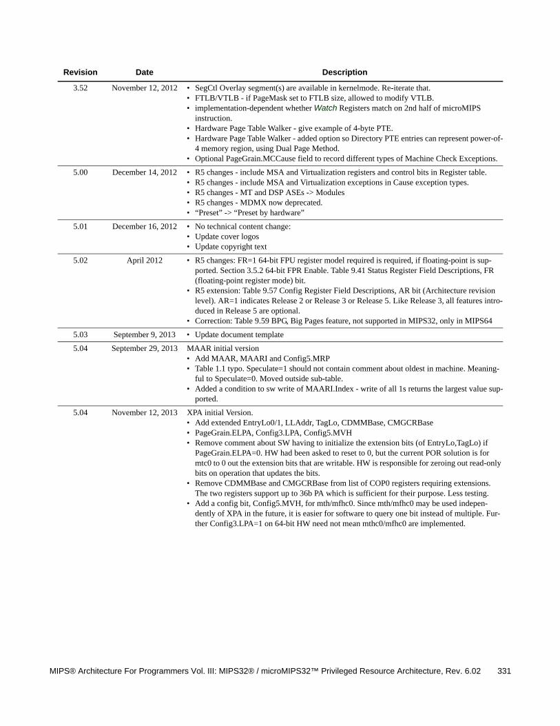
MIPS® Architecture For Programmers Vol. III: MIPS32® / microMIPS32™ Privileged Resource Architecture, Rev. 6.02 331
3.52 November 12, 2012 • SegCtl Overlay segment(s) are available in kernelmode. Re-iterate that. • FTLB/VTLB - if PageMask set to FTLB size, allowed to modify VTLB. • implementation-dependent whether Watch Registers match on 2nd half of microMIPS
instruction. • Hardware Page Table Walker - give example of 4-byte PTE. • Hardware Page Table Walker - added option so Directory PTE entries can represent power-of-
4 memory region, using Dual Page Method. • Optional PageGrain.MCCause field to record different types of Machine Check Exceptions.
5.00 December 14, 2012 • R5 changes - include MSA and Virtualization registers and control bits in Register table. • R5 changes - include MSA and Virtualization exceptions in Cause exception types. • R5 changes - MT and DSP ASEs -> Modules • R5 changes - MDMX now deprecated. • “Preset” -> “Preset by hardware”
5.01 December 16, 2012 • No technical content change: • Update cover logos• Update copyright text
5.02 April 2012 • R5 changes: FR=1 64-bit FPU register model required is required, if floating-point is sup-ported. Section 3.5.2 64-bit FPR Enable. Table 9.41 Status Register Field Descriptions, FR (floating-point register mode) bit.
• R5 extension: Table 9.57 Config Register Field Descriptions, AR bit (Architecture revision level). AR=1 indicates Release 2 or Release 3 or Release 5. Like Release 3, all features intro-duced in Release 5 are optional.
• Correction: Table 9.59 BPG, Big Pages feature, not supported in MIPS32, only in MIPS64
5.03 September 9, 2013 • Update document template
5.04 September 29, 2013 MAAR initial version• Add MAAR, MAARI and Config5.MRP• Table 1.1 typo. Speculate=1 should not contain comment about oldest in machine. Meaning-
ful to Speculate=0. Moved outside sub-table.• Added a condition to sw write of MAARI.Index - write of all 1s returns the largest value sup-
ported.
5.04 November 12, 2013 XPA initial Version.• Add extended EntryLo0/1, LLAddr, TagLo, CDMMBase, CMGCRBase • PageGrain.ELPA, Config3.LPA, Config5.MVH• Remove comment about SW having to initialize the extension bits (of EntryLo,TagLo) if
PageGrain.ELPA=0. HW had been asked to reset to 0, but the current POR solution is for mtc0 to 0 out the extension bits that are writable. HW is responsible for zeroing out read-only bits on operation that updates the bits.
• Remove CDMMBase and CMGCRBase from list of COP0 registers requiring extensions. The two registers support up to 36b PA which is sufficient for their purpose. Less testing.
• Add a config bit, Config5.MVH, for mth/mfhc0. Since mth/mfhc0 may be used indepen-dently of XPA in the future, it is easier for software to query one bit instead of multiple. Fur-ther Config3.LPA=1 on 64-bit HW need not mean mthc0/mfhc0 are implemented.
Revision Date Description
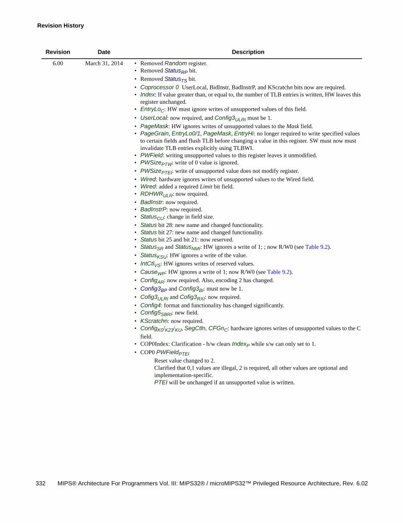
Revision History
332 MIPS® Architecture For Programmers Vol. III: MIPS32® / microMIPS32™ Privileged Resource Architecture, Rev. 6.02
6.00 March 31, 2014 • Removed Random register.• Removed StatusRP bit.
• Removed StatusTS bit.
• Coprocessor 0 UserLocal, BidInstr, BadInstrP, and KScratchn bits now are required.• Index: If value greater than, or equal to, the number of TLB entries is written, HW leaves this
register unchanged.• EntryLoC: HW must ignore writes of unsupported values of this field.
• UserLocal: now required, and Config3ULRI must be 1.
• PageMask: HW ignores writes of unsupported values to the Mask field.• PageGrain, EntryLo0/1, PageMask, EntryHi: no longer required to write specified values
to certain fields and flush TLB before changing a value in this register. SW must now must invalidate TLB entries explicitly using TLBWI.
• PWField: writing unsupported values to this register leaves it unmodified.• PWSizePTW: write of 0 value is ignored.
• PWSizePTEI: write of unsupported value does not modify register.
• Wired: hardware ignores writes of unsupported values to the Wired field. • Wired: added a required Limit bit field.• RDHWRULR: now required.
• BadInstr: now required.• BadInstrP: now required.• StatusCU: change in field size.
• Status bit 28: new name and changed functionality.• Status bit 27: new name and changed functionality.• Status bit 25 and bit 21: now reserved.• StatusSR and StatusNMI: HW ignores a write of 1; ; now R/W0 (see Table 9.2).
• StatusKSU: HW ignores a write of the value.
• IntCtlVS: HW ignores writes of reserved values.
• CauseWP: HW ignores a write of 1; now R/W0 (see Table 9.2).
• ConfigAR: now required. Also, encoding 2 has changed.
• Config3BP and Config3BI: must now be 1.
• Cofig3ULRI and Cofig3RXI: now required.
• Config4: format and functionality has changed significantly.• Config5SBRI: new field.
• KScratchn: now required.• ConfigK0/K23/KU, SegCtln, CFGnC: hardware ignores writes of unsupported values to the C
field.• COP0Index: Clarification - h/w clears IndexP while s/w can only set to 1.
• COP0 PWFieldPTEI
Reset value changed to 2.Clarified that 0,1 values are illegal, 2 is required, all other values are optional andimplementation-specific.PTEI will be unchanged if an unsupported value is written.
Revision Date Description
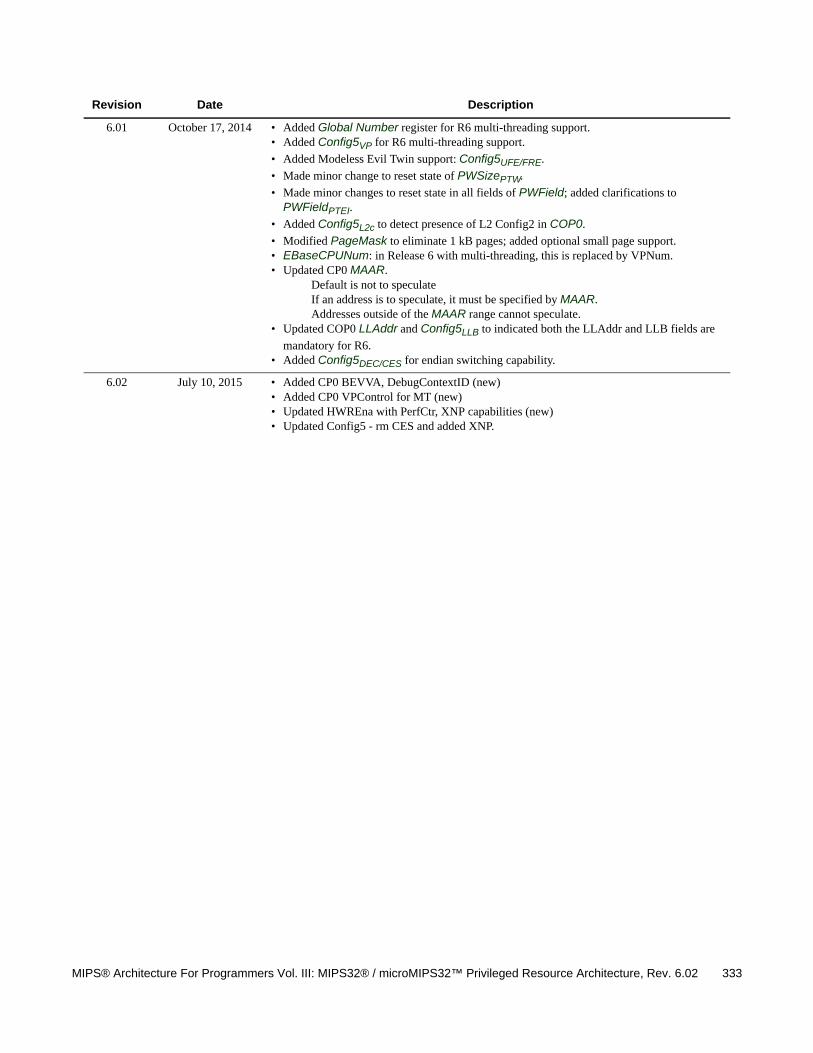
MIPS® Architecture For Programmers Vol. III: MIPS32® / microMIPS32™ Privileged Resource Architecture, Rev. 6.02 333
6.01 October 17, 2014 • Added Global Number register for R6 multi-threading support.• Added Config5VP for R6 multi-threading support.
• Added Modeless Evil Twin support: Config5UFE/FRE.
• Made minor change to reset state of PWSizePTW.
• Made minor changes to reset state in all fields of PWField; added clarifications to PWFieldPTEI.
• Added Config5L2c to detect presence of L2 Config2 in COP0.
• Modified PageMask to eliminate 1 kB pages; added optional small page support. • EBaseCPUNum: in Release 6 with multi-threading, this is replaced by VPNum. • Updated CP0 MAAR.
Default is not to speculate If an address is to speculate, it must be specified by MAAR. Addresses outside of the MAAR range cannot speculate.
• Updated COP0 LLAddr and Config5LLB to indicated both the LLAddr and LLB fields are
mandatory for R6.• Added Config5DEC/CES for endian switching capability.
6.02 July 10, 2015 • Added CP0 BEVVA, DebugContextID (new)• Added CP0 VPControl for MT (new)• Updated HWREna with PerfCtr, XNP capabilities (new)• Updated Config5 - rm CES and added XNP.
Revision Date Description
Revision History
334 MIPS® Architecture For Programmers Vol. III: MIPS32® / microMIPS32™ Privileged Resource Architecture, Rev. 6.02
Copyright © Wave Computing, Inc. All rights reserved. www.wavecomp.ai