micron serial nor flash memory - micron technology,...
TRANSCRIPT
Micron Serial NOR Flash Memory1.8V, Multiple I/O, 4KB Sector EraseN25Q016A11E
Features• SPI-compatible serial bus interface• 108 MHz (MAX) clock frequency• 1.7–2.0V single supply voltage• Dual/quad I/O instruction provides increased
throughput up to 432 MB/s• Supported protocols
– Extended SPI, dual I/O, and quad I/O• Execute-in-place (XIP) mode for all three protocols
– Configurable via volatile or nonvolatile registers– Enables memory to work in XIP mode directly af-
ter power-on• PROGRAM/ERASE SUSPEND operations• Continuous read of entire memory via a single com-
mand– Fast read– Quad or dual output fast read– Quad or dual I/O fast read
• Flexible to fit application– Configurable number of dummy cycles– Output buffer configurable
• Software reset• Hardware RESET function available upon customer
request• 64-byte, user-lockable, one-time programmable
(OTP) dedicated area• Erase capability
– Subsector erase 4KB uniform granularity blocks– Subsector erase 32KB uniform granularity blocks– Sector erase 64KB uniform granularity blocks
• Deep power-down mode: 5µA (TYP)• Write protection
– Software write protection applicable to every64KB sector via volatile lock bit
– Hardware write protection: protected area sizedefined by five nonvolatile bits (BP0, BP1, BP2,and TB)
– Additional smart protections, available upon re-quest
• Electronic signature– JEDEC-standard 2-byte signature (BB15h)– Two additional extended device ID (EDID) bytes
to identify device factory options– Unique ID code (UID): 14 read-only bytes
• Minimum 100,000 ERASE cycles per sector• More than 20 years data retention• Packages JEDEC standard, all RoHS compliant
– F4 = U-PDFN-8/4mm x 3mm (MLP8)– F6 = V-PDFN-8/6mm x 5mm (MLP8)– SC = SOP2-8/150 mil (SO8N)– 51 = XF-SCSP-8/2mm x 2.8mm (XFCSP)
16Mb, Multiple I/O Serial Flash MemoryFeatures
09005aef84a4754fn25q_16mb_1_8v_65nm.pdf - Rev. H 01/18 EN 1 Micron Technology, Inc. reserves the right to change products or specifications without notice.
© 2012 Micron Technology, Inc. All rights reserved.
Products and specifications discussed herein are subject to change by Micron without notice.
ContentsImportant Notes and Warnings ......................................................................................................................... 6Device Description ........................................................................................................................................... 7
Features ....................................................................................................................................................... 73-Byte Address Modes .................................................................................................................................. 7Operating Protocols ...................................................................................................................................... 7XIP Mode ..................................................................................................................................................... 7Device Configurability .................................................................................................................................. 8
Signal Assignments ........................................................................................................................................... 9Signal Descriptions ......................................................................................................................................... 10Memory Organization .................................................................................................................................... 12
Memory Configuration and Block Diagram .................................................................................................. 12Memory Map ............................................................................................................................................. 13
Device Protection ........................................................................................................................................... 14Serial Peripheral Interface Modes .................................................................................................................... 16SPI Protocols .................................................................................................................................................. 18Nonvolatile and Volatile Registers ................................................................................................................... 19
Status Register ............................................................................................................................................ 20Nonvolatile and Volatile Configuration Registers .......................................................................................... 21Enhanced Volatile Configuration Register .................................................................................................... 24Flag Status Register ..................................................................................................................................... 25
Command Definitions .................................................................................................................................... 26READ REGISTER and WRITE REGISTER Operations ........................................................................................ 28
READ STATUS REGISTER or FLAG STATUS REGISTER Command ................................................................ 28READ NONVOLATILE CONFIGURATION REGISTER Command ................................................................... 29READ VOLATILE or ENHANCED VOLATILE CONFIGURATION REGISTER Command .................................. 29WRITE STATUS REGISTER Command ......................................................................................................... 29WRITE NONVOLATILE CONFIGURATION REGISTER Command ................................................................. 30WRITE VOLATILE or ENHANCED VOLATILE CONFIGURATION REGISTER Command ................................. 30READ LOCK REGISTER Command .............................................................................................................. 31WRITE LOCK REGISTER Command ............................................................................................................ 32CLEAR FLAG STATUS REGISTER Command ................................................................................................ 33
READ IDENTIFICATION Operations ............................................................................................................... 34READ ID and MULTIPLE I/O READ ID Commands ...................................................................................... 34READ SERIAL FLASH DISCOVERY PARAMETER Command ......................................................................... 35
READ MEMORY Operations ............................................................................................................................ 39PROGRAM Operations .................................................................................................................................... 43WRITE Operations .......................................................................................................................................... 48
WRITE ENABLE Command ......................................................................................................................... 48WRITE DISABLE Command ........................................................................................................................ 48
ERASE Operations .......................................................................................................................................... 50SUBSECTOR ERASE Command ................................................................................................................... 50SECTOR ERASE Command ......................................................................................................................... 50BULK ERASE Command ............................................................................................................................. 51PROGRAM/ERASE SUSPEND Command ..................................................................................................... 52PROGRAM/ERASE RESUME Command ...................................................................................................... 54
RESET Operations .......................................................................................................................................... 55RESET ENABLE and RESET MEMORY Command ........................................................................................ 55RESET Conditions ...................................................................................................................................... 55
ONE TIME PROGRAMMABLE Operations ....................................................................................................... 56READ OTP ARRAY Command ...................................................................................................................... 56
16Mb, Multiple I/O Serial Flash MemoryFeatures
09005aef84a4754fn25q_16mb_1_8v_65nm.pdf - Rev. H 01/18 EN 2 Micron Technology, Inc. reserves the right to change products or specifications without notice.
© 2012 Micron Technology, Inc. All rights reserved.
PROGRAM OTP ARRAY Command .............................................................................................................. 56XIP Mode ....................................................................................................................................................... 58
Activate or Terminate XIP Using Volatile Configuration Register ................................................................... 58Activate or Terminate XIP Using Nonvolatile Configuration Register ............................................................. 58Confirmation Bit Settings Required to Activate or Terminate XIP .................................................................. 59Terminating XIP After a Controller and Memory Reset ................................................................................. 59
Power Up and Power Down ............................................................................................................................. 61Power Up and Power Down Requirements ................................................................................................... 61Power Loss Recovery Sequence ................................................................................................................... 62
AC Reset Specifications ................................................................................................................................... 63Absolute Ratings and Operating Conditions ..................................................................................................... 67DC Characteristics and Operating Conditions .................................................................................................. 69AC Characteristics and Operating Conditions .................................................................................................. 70Package Dimensions ....................................................................................................................................... 72Part Number Ordering Information ................................................................................................................. 76Revision History ............................................................................................................................................. 77
Rev. H – 2/2018 ........................................................................................................................................... 77Rev. G – 1/2016 ........................................................................................................................................... 77Rev. F – 1/2014 ........................................................................................................................................... 77Rev. E – 7/2013 ........................................................................................................................................... 77Rev. D – 7/2012 ........................................................................................................................................... 77Rev. C – 6/2012 ........................................................................................................................................... 77Rev. B – 5/2012 ........................................................................................................................................... 77Rev. A – 2/2012 ........................................................................................................................................... 77
16Mb, Multiple I/O Serial Flash MemoryFeatures
09005aef84a4754fn25q_16mb_1_8v_65nm.pdf - Rev. H 01/18 EN 3 Micron Technology, Inc. reserves the right to change products or specifications without notice.
© 2012 Micron Technology, Inc. All rights reserved.
List of FiguresFigure 1: Logic Diagram ................................................................................................................................... 8Figure 2: SO8N, MLP8 TSOP (Top View) ........................................................................................................... 9Figure 3: 8-Balls, XFCSP, 2mm x 2.8mm x 0.37mm (Top View) ........................................................................... 9Figure 4: Block Diagram ................................................................................................................................ 12Figure 5: Bus Master and Memory Devices on the SPI Bus ............................................................................... 17Figure 6: SPI Modes ....................................................................................................................................... 17Figure 7: Internal Configuration Register ........................................................................................................ 19Figure 8: READ REGISTER Command ............................................................................................................ 28Figure 9: WRITE REGISTER Command ........................................................................................................... 30Figure 10: READ LOCK REGISTER Command ................................................................................................. 32Figure 11: WRITE LOCK REGISTER Command ............................................................................................... 33Figure 12: READ ID and MULTIPLE I/O Read ID Commands .......................................................................... 35Figure 13: READ Command ........................................................................................................................... 40Figure 14: FAST READ Command ................................................................................................................... 40Figure 15: DUAL OUTPUT FAST READ ........................................................................................................... 41Figure 16: DUAL INPUT/OUTPUT FAST READ Command .............................................................................. 41Figure 17: QUAD OUTPUT FAST READ Command ......................................................................................... 42Figure 18: QUAD INPUT/OUTPUT FAST READ Command ............................................................................. 42Figure 19: PAGE PROGRAM Command .......................................................................................................... 44Figure 20: DUAL INPUT FAST PROGRAM Command ...................................................................................... 45Figure 21: EXTENDED DUAL INPUT FAST PROGRAM Command ................................................................... 45Figure 22: QUAD INPUT FAST PROGRAM Command ..................................................................................... 46Figure 23: EXTENDED QUAD INPUT FAST PROGRAM Command ................................................................... 47Figure 24: WRITE ENABLE and WRITE DISABLE Command Sequence ............................................................ 49Figure 25: SUBSECTOR and SECTOR ERASE Command .................................................................................. 51Figure 26: BULK ERASE Command ................................................................................................................ 52Figure 27: RESET ENABLE and RESET MEMORY Command ........................................................................... 55Figure 28: READ OTP Command .................................................................................................................... 56Figure 29: PROGRAM OTP Command ............................................................................................................ 57Figure 30: XIP Mode Directly After Power-On .................................................................................................. 59Figure 31: Power-Up Timing .......................................................................................................................... 61Figure 32: Reset AC Timing During PROGRAM or ERASE Cycle ........................................................................ 64Figure 33: Reset Enable ................................................................................................................................. 64Figure 34: Serial Input Timing ........................................................................................................................ 64Figure 35: Write Protect Setup and Hold During WRITE STATUS REGISTER Operation (SRWD = 1) ................... 65Figure 36: Hold Timing .................................................................................................................................. 65Figure 37: Output Timing .............................................................................................................................. 66Figure 38: VPPH Timing .................................................................................................................................. 66Figure 39: AC Timing Input/Output Reference Levels ...................................................................................... 68Figure 40: UFDFPN8-4×3 mm ........................................................................................................................ 72Figure 41: DFN-6 x 5mm ................................................................................................................................ 73Figure 42: S08N-150mils ................................................................................................................................ 74Figure 43: XFCSP-2x2.8mm ............................................................................................................................ 75
16Mb, Multiple I/O Serial Flash MemoryFeatures
09005aef84a4754fn25q_16mb_1_8v_65nm.pdf - Rev. H 01/18 EN 4 Micron Technology, Inc. reserves the right to change products or specifications without notice.
© 2012 Micron Technology, Inc. All rights reserved.
List of TablesTable 1: Signal Descriptions ........................................................................................................................... 10Table 2: Sectors 31 : 0 ..................................................................................................................................... 13Table 3: Data Protection using Device Protocols ............................................................................................. 14Table 4: Memory Sector Protection Truth Table .............................................................................................. 14Table 5: Protected Area Sizes – Upper Area ..................................................................................................... 15Table 6: Protected Area Sizes – Lower Area ...................................................................................................... 15Table 7: SPI Modes ........................................................................................................................................ 16Table 8: Extended, Dual, and Quad SPI Protocols ............................................................................................ 18Table 9: Status Register Bit Definitions ........................................................................................................... 20Table 10: Nonvolatile Configuration Register Bit Definitions ........................................................................... 21Table 11: Volatile Configuration Register Bit Definitions .................................................................................. 22Table 12: Sequence of Bytes During Wrap ....................................................................................................... 23Table 13: Supported Clock Frequencies .......................................................................................................... 23Table 14: Enhanced Volatile Configuration Register Bit Definitions .................................................................. 24Table 15: Flag Status Register Bit Definitions .................................................................................................. 25Table 16: Command Set ................................................................................................................................. 26Table 17: Lock Register .................................................................................................................................. 31Table 18: Data/Address Lines for READ ID and MULTIPLE I/O READ ID Commands ....................................... 34Table 19: Read ID Data Out ............................................................................................................................ 34Table 20: Extended Device ID, First Byte ......................................................................................................... 34Table 21: Serial Flash Discovery Parameter Data Structure .............................................................................. 36Table 22: Parameter ID .................................................................................................................................. 37Table 23: Command/Address/Data Lines for READ MEMORY Commands ....................................................... 39Table 24: Data/Address Lines for PROGRAM Commands ................................................................................ 43Table 25: Suspend Parameters ....................................................................................................................... 53Table 26: Operations Allowed/Disallowed During Device States ...................................................................... 53Table 27: Reset Command Set ........................................................................................................................ 55Table 28: OTP Control Byte (Byte 64) .............................................................................................................. 57Table 29: XIP Confirmation Bit ....................................................................................................................... 59Table 30: Effects of Running XIP in Different Protocols .................................................................................... 59Table 31: Power-Up Timing and VWI Threshold ............................................................................................... 62Table 32: AC RESET Conditions ...................................................................................................................... 63Table 33: Absolute Ratings ............................................................................................................................. 67Table 34: Operating Conditions ...................................................................................................................... 67Table 35: Input/Output Capacitance .............................................................................................................. 67Table 36: AC Timing Input/Output Conditions ............................................................................................... 68Table 37: DC Current Characteristics and Operating Conditions ...................................................................... 69Table 38: DC Voltage Characteristics and Operating Conditions ...................................................................... 69Table 39: AC Characteristics and Operating Conditions ................................................................................... 70Table 40: Part Number Information ................................................................................................................ 76Table 41: Package Details ............................................................................................................................... 76
16Mb, Multiple I/O Serial Flash MemoryFeatures
09005aef84a4754fn25q_16mb_1_8v_65nm.pdf - Rev. H 01/18 EN 5 Micron Technology, Inc. reserves the right to change products or specifications without notice.
© 2012 Micron Technology, Inc. All rights reserved.
Important Notes and WarningsMicron Technology, Inc. ("Micron") reserves the right to make changes to information published in this document,including without limitation specifications and product descriptions. This document supersedes and replaces allinformation supplied prior to the publication hereof. You may not rely on any information set forth in this docu-ment if you obtain the product described herein from any unauthorized distributor or other source not authorizedby Micron.
Automotive Applications. Products are not designed or intended for use in automotive applications unless specifi-cally designated by Micron as automotive-grade by their respective data sheets. Distributor and customer/distrib-utor shall assume the sole risk and liability for and shall indemnify and hold Micron harmless against all claims,costs, damages, and expenses and reasonable attorneys' fees arising out of, directly or indirectly, any claim ofproduct liability, personal injury, death, or property damage resulting directly or indirectly from any use of non-automotive-grade products in automotive applications. Customer/distributor shall ensure that the terms and con-ditions of sale between customer/distributor and any customer of distributor/customer (1) state that Micronproducts are not designed or intended for use in automotive applications unless specifically designated by Micronas automotive-grade by their respective data sheets and (2) require such customer of distributor/customer to in-demnify and hold Micron harmless against all claims, costs, damages, and expenses and reasonable attorneys'fees arising out of, directly or indirectly, any claim of product liability, personal injury, death, or property damageresulting from any use of non-automotive-grade products in automotive applications.
Critical Applications. Products are not authorized for use in applications in which failure of the Micron compo-nent could result, directly or indirectly in death, personal injury, or severe property or environmental damage("Critical Applications"). Customer must protect against death, personal injury, and severe property and environ-mental damage by incorporating safety design measures into customer's applications to ensure that failure of theMicron component will not result in such harms. Should customer or distributor purchase, use, or sell any Microncomponent for any critical application, customer and distributor shall indemnify and hold harmless Micron andits subsidiaries, subcontractors, and affiliates and the directors, officers, and employees of each against all claims,costs, damages, and expenses and reasonable attorneys' fees arising out of, directly or indirectly, any claim ofproduct liability, personal injury, or death arising in any way out of such critical application, whether or not Mi-cron or its subsidiaries, subcontractors, or affiliates were negligent in the design, manufacture, or warning of theMicron product.
Customer Responsibility. Customers are responsible for the design, manufacture, and operation of their systems,applications, and products using Micron products. ALL SEMICONDUCTOR PRODUCTS HAVE INHERENT FAIL-URE RATES AND LIMITED USEFUL LIVES. IT IS THE CUSTOMER'S SOLE RESPONSIBILITY TO DETERMINEWHETHER THE MICRON PRODUCT IS SUITABLE AND FIT FOR THE CUSTOMER'S SYSTEM, APPLICATION, ORPRODUCT. Customers must ensure that adequate design, manufacturing, and operating safeguards are includedin customer's applications and products to eliminate the risk that personal injury, death, or severe property or en-vironmental damages will result from failure of any semiconductor component.
Limited Warranty. In no event shall Micron be liable for any indirect, incidental, punitive, special or consequentialdamages (including without limitation lost profits, lost savings, business interruption, costs related to the removalor replacement of any products or rework charges) whether or not such damages are based on tort, warranty,breach of contract or other legal theory, unless explicitly stated in a written agreement executed by Micron's dulyauthorized representative.
16Mb, Multiple I/O Serial Flash MemoryImportant Notes and Warnings
09005aef84a4754fn25q_16mb_1_8v_65nm.pdf - Rev. H 01/18 EN 6 Micron Technology, Inc. reserves the right to change products or specifications without notice.
© 2012 Micron Technology, Inc. All rights reserved.
Device DescriptionThe N25Q is the first high-performance multiple input/output serial Flash memory de-vice manufactured on 65nm NOR technology. It features execute-in-place (XIP) func-tionality, advanced write protection mechanisms, and a high-speed SPI-compatible businterface. The innovative, high-performance, dual and quad input/output instructionsenable double or quadruple the transfer bandwidth for READ and PROGRAM opera-tions.
Features
The memory is organized as 32 (64KB) main sectors that are divided into two subsectorseach (32KB), that are further divided into eight 4KB subsectors each, 512 4KB subsec-tors in total. The memory can be erased one 4KB subsector at a time, one 32KB subsec-tor at a time, one 64KB sector at a time, or as a whole.
The memory can be write protected by software through volatile and nonvolatile pro-tection features, depending on the application needs. The protection granularity is of64KB (sector granularity) for volatile protections
The device has 64 one-time programmable (OTP) bytes that can be read and program-med with the READ OTP and PROGRAM OTP commands. These 64 bytes can also bepermanently locked with a PROGRAM OTP command.
The device also has the ability to pause and resume PROGRAM and ERASE cycles by us-ing dedicated PROGRAM/ERASE SUSPEND and RESUME instructions.
3-Byte Address Modes
The device features 3-byte address modes to access the memory.
Operating Protocols
The memory can be operated with three different protocols:
• Extended SPI (standard SPI protocol upgraded with dual and quad operations)• Dual I/O SPI• Quad I/O SPI
The standard SPI protocol is extended and enhanced by dual and quad operations. Inaddition, the dual SPI and quad SPI protocols improve the data access time andthroughput of a single I/O device by transmitting commands, addresses, and dataacross two or four data lines.
XIP Mode
XIP mode requires only an address (no instruction) to output data, improving randomaccess time and eliminating the need to shadow code onto RAM for fast execution.
All protocols support XIP operation. For flexibility, multiple XIP entry and exit methodsare available. For applications that must enter XIP mode immediately after poweringup, XIP mode can be set as the default mode through the nonvolatile configuration reg-ister bits.
16Mb, Multiple I/O Serial Flash MemoryDevice Description
09005aef84a4754fn25q_16mb_1_8v_65nm.pdf - Rev. H 01/18 EN 7 Micron Technology, Inc. reserves the right to change products or specifications without notice.
© 2012 Micron Technology, Inc. All rights reserved.
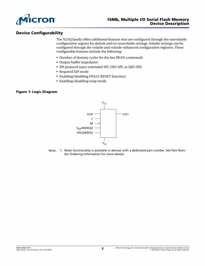
Device Configurability
The N25Q family offers additional features that are configured through the nonvolatileconfiguration register for default and/or nonvolatile settings. Volatile settings can beconfigured through the volatile and volatile-enhanced configuration registers. Theseconfigurable features include the following:
• Number of dummy cycles for the fast READ commands• Output buffer impedance• SPI protocol types (extended SPI, DIO-SPI, or QIO-SPI)• Required XIP mode• Enabling/disabling HOLD (RESET function)• Enabling/disabling wrap mode
Figure 1: Logic Diagram
VCC
DQ0
C
S#
VPP/W#/DQ2
HOLD#/DQ3
VSS
DQ1
Note: 1. Reset functionality is available in devices with a dedicated part number. See Part Num-ber Ordering Information for more details.
16Mb, Multiple I/O Serial Flash MemoryDevice Description
09005aef84a4754fn25q_16mb_1_8v_65nm.pdf - Rev. H 01/18 EN 8 Micron Technology, Inc. reserves the right to change products or specifications without notice.
© 2012 Micron Technology, Inc. All rights reserved.
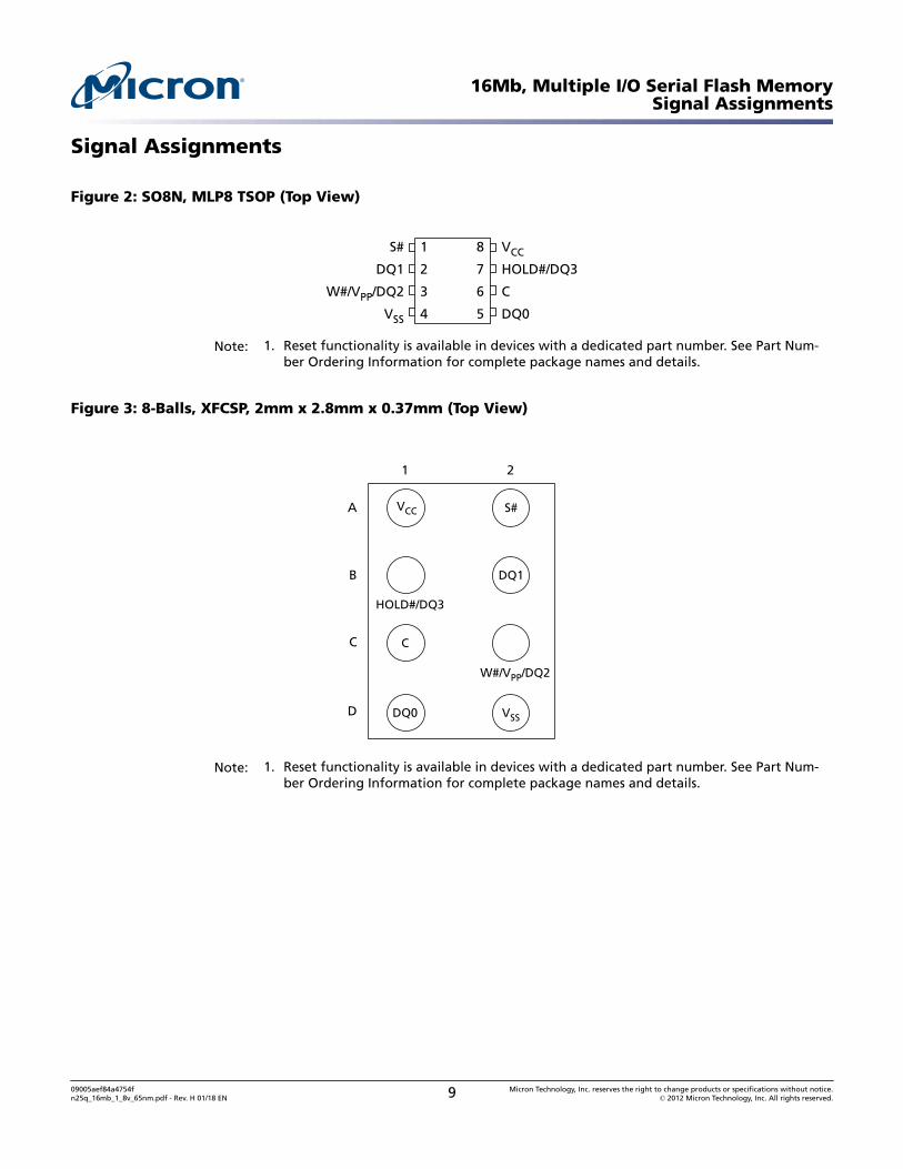
Signal Assignments
Figure 2: SO8N, MLP8 TSOP (Top View)
1
2
3
4
8
7
6
5
S#
DQ1
W#/VPP/DQ2
VSS
VCC
HOLD#/DQ3
C
DQ0
Note: 1. Reset functionality is available in devices with a dedicated part number. See Part Num-ber Ordering Information for complete package names and details.
Figure 3: 8-Balls, XFCSP, 2mm x 2.8mm x 0.37mm (Top View)
A
1 2
B
C
D
VCC S#
DQ1
DQ0
HOLD#/DQ3
C
W#/VPP/DQ2
VSS
Note: 1. Reset functionality is available in devices with a dedicated part number. See Part Num-ber Ordering Information for complete package names and details.
16Mb, Multiple I/O Serial Flash MemorySignal Assignments
09005aef84a4754fn25q_16mb_1_8v_65nm.pdf - Rev. H 01/18 EN 9 Micron Technology, Inc. reserves the right to change products or specifications without notice.
© 2012 Micron Technology, Inc. All rights reserved.
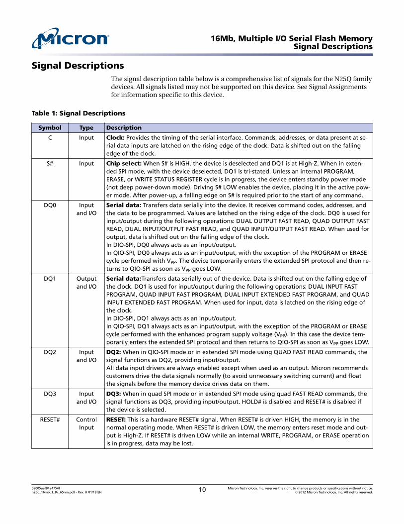
Signal DescriptionsThe signal description table below is a comprehensive list of signals for the N25Q familydevices. All signals listed may not be supported on this device. See Signal Assignmentsfor information specific to this device.
Table 1: Signal Descriptions
Symbol Type Description
C Input Clock: Provides the timing of the serial interface. Commands, addresses, or data present at se-rial data inputs are latched on the rising edge of the clock. Data is shifted out on the fallingedge of the clock.
S# Input Chip select: When S# is HIGH, the device is deselected and DQ1 is at High-Z. When in exten-ded SPI mode, with the device deselected, DQ1 is tri-stated. Unless an internal PROGRAM,ERASE, or WRITE STATUS REGISTER cycle is in progress, the device enters standby power mode(not deep power-down mode). Driving S# LOW enables the device, placing it in the active pow-er mode. After power-up, a falling edge on S# is required prior to the start of any command.
DQ0 Inputand I/O
Serial data: Transfers data serially into the device. It receives command codes, addresses, andthe data to be programmed. Values are latched on the rising edge of the clock. DQ0 is used forinput/output during the following operations: DUAL OUTPUT FAST READ, QUAD OUTPUT FASTREAD, DUAL INPUT/OUTPUT FAST READ, and QUAD INPUT/OUTPUT FAST READ. When used foroutput, data is shifted out on the falling edge of the clock.In DIO-SPI, DQ0 always acts as an input/output.In QIO-SPI, DQ0 always acts as an input/output, with the exception of the PROGRAM or ERASEcycle performed with VPP. The device temporarily enters the extended SPI protocol and then re-turns to QIO-SPI as soon as VPP goes LOW.
DQ1 Outputand I/O
Serial data:Transfers data serially out of the device. Data is shifted out on the falling edge ofthe clock. DQ1 is used for input/output during the following operations: DUAL INPUT FASTPROGRAM, QUAD INPUT FAST PROGRAM, DUAL INPUT EXTENDED FAST PROGRAM, and QUADINPUT EXTENDED FAST PROGRAM. When used for input, data is latched on the rising edge ofthe clock.In DIO-SPI, DQ1 always acts as an input/output.In QIO-SPI, DQ1 always acts as an input/output, with the exception of the PROGRAM or ERASEcycle performed with the enhanced program supply voltage (VPP). In this case the device tem-porarily enters the extended SPI protocol and then returns to QIO-SPI as soon as VPP goes LOW.
DQ2 Inputand I/O
DQ2: When in QIO-SPI mode or in extended SPI mode using QUAD FAST READ commands, thesignal functions as DQ2, providing input/output.All data input drivers are always enabled except when used as an output. Micron recommendscustomers drive the data signals normally (to avoid unnecessary switching current) and floatthe signals before the memory device drives data on them.
DQ3 Inputand I/O
DQ3: When in quad SPI mode or in extended SPI mode using quad FAST READ commands, thesignal functions as DQ3, providing input/output. HOLD# is disabled and RESET# is disabled ifthe device is selected.
RESET# ControlInput
RESET: This is a hardware RESET# signal. When RESET# is driven HIGH, the memory is in thenormal operating mode. When RESET# is driven LOW, the memory enters reset mode and out-put is High-Z. If RESET# is driven LOW while an internal WRITE, PROGRAM, or ERASE operationis in progress, data may be lost.
16Mb, Multiple I/O Serial Flash MemorySignal Descriptions
09005aef84a4754fn25q_16mb_1_8v_65nm.pdf - Rev. H 01/18 EN 10 Micron Technology, Inc. reserves the right to change products or specifications without notice.
© 2012 Micron Technology, Inc. All rights reserved.
Table 1: Signal Descriptions (Continued)
Symbol Type Description
HOLD# ControlInput
HOLD: Pauses any serial communications with the device without deselecting the device. DQ1(output) is High-Z. DQ0 (input) and the clock are "Don't Care." To enable HOLD, the devicemust be selected with S# driven LOW.HOLD# is used for input/output during the following operations: QUAD OUTPUT FAST READ,QUAD INPUT/OUTPUT FAST READ, QUAD INPUT FAST PROGRAM, and QUAD INPUT EXTENDEDFAST PROGRAM.In QIO-SPI, HOLD# acts as an I/O (DQ3 functionality), and the HOLD# functionality is disabledwhen the device is selected. When the device is deselected (S# is HIGH) in parts with RESET#functionality, it is possible to reset the device unless this functionality is not disabled by meansof dedicated registers bits.The HOLD# functionality can be disabled using bit 4 of the NVCR or bit 4 of the VECR.
W# ControlInput
Write protect: W# can be used as a protection control input or in QIO-SPI operations. When inextended SPI with single or dual commands, the WRITE PROTECT function is selectable by thevoltage range applied to the signal. If voltage range is low (0V to VCC), the signal acts as awrite protection control input. The memory size protected against PROGRAM or ERASE opera-tions is locked as specified in the status register block protect bits 3:0.W# is used as an input/output (DQ2 functionality) during QUAD INPUT FAST READ and QUADINPUT/OUTPUT FAST READ operations and in QIO-SPI.
VPP Power Supply voltage: If VPP is in the voltage range of VPPH, the signal acts as an additional powersupply, as defined in the AC Measurement Conditions table.During QIFP, QIEFP, and QIO-SPI PROGRAM/ERASE operations, it is possible to use the addition-al VPP power supply to speed up internal operations. However, to enable this functionality, it isnecessary to set bit 3 of the VECR to 0.In this case, VPP is used as an I/O until the end of the operation. After the last input data is shif-ted in, the application should apply VPP voltage to VPP within 200ms to speed up the internaloperations. If the VPP voltage is not applied within 200ms, the PROGRAM/ERASE operationsstart at standard speed.The default value of VECR bit 3 is 1, and the VPP functionality for quad I/O modify operations isdisabled.
VCC Power Device core power supply: Source voltage.
VSS Ground Ground: Reference for the VCC supply voltage.
DNU – Do not use.
NC – No connect.
16Mb, Multiple I/O Serial Flash MemorySignal Descriptions
09005aef84a4754fn25q_16mb_1_8v_65nm.pdf - Rev. H 01/18 EN 11 Micron Technology, Inc. reserves the right to change products or specifications without notice.
© 2012 Micron Technology, Inc. All rights reserved.
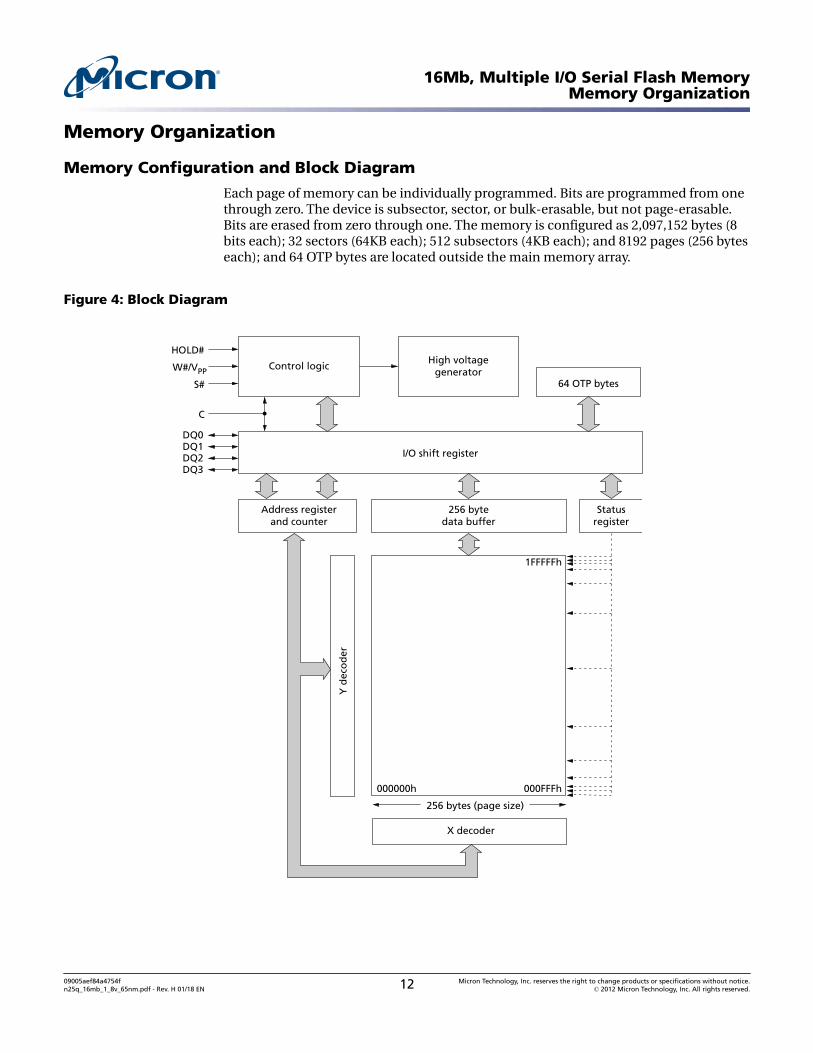
Memory Organization
Memory Configuration and Block Diagram
Each page of memory can be individually programmed. Bits are programmed from onethrough zero. The device is subsector, sector, or bulk-erasable, but not page-erasable.Bits are erased from zero through one. The memory is configured as 2,097,152 bytes (8bits each); 32 sectors (64KB each); 512 subsectors (4KB each); and 8192 pages (256 byteseach); and 64 OTP bytes are located outside the main memory array.
Figure 4: Block Diagram
HOLD#
S#
W#/VPP Control logicHigh voltage
generator
I/O shift register
Address registerand counter
256 bytedata buffer
256 bytes (page size)
X decoder
Y d
eco
der
C
Statusregister
000000h
1FFFFFh
000FFFh
64 OTP bytes
DQ0DQ1DQ2DQ3
16Mb, Multiple I/O Serial Flash MemoryMemory Organization
09005aef84a4754fn25q_16mb_1_8v_65nm.pdf - Rev. H 01/18 EN 12 Micron Technology, Inc. reserves the right to change products or specifications without notice.
© 2012 Micron Technology, Inc. All rights reserved.
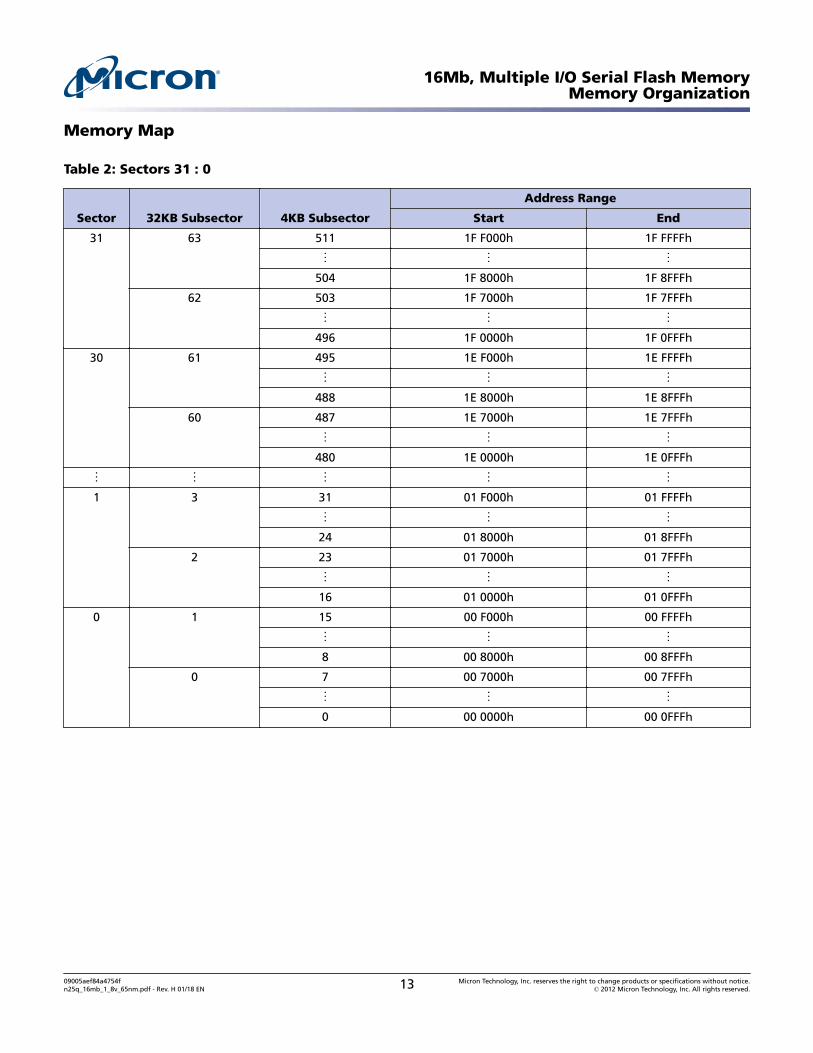
Memory Map
Table 2: Sectors 31 : 0
Sector 32KB Subsector 4KB Subsector
Address Range
Start End
31 63 511 1F F000h 1F FFFFh
⋮ ⋮ ⋮504 1F 8000h 1F 8FFFh
62 503 1F 7000h 1F 7FFFh
⋮ ⋮ ⋮496 1F 0000h 1F 0FFFh
30 61 495 1E F000h 1E FFFFh
⋮ ⋮ ⋮488 1E 8000h 1E 8FFFh
60 487 1E 7000h 1E 7FFFh
⋮ ⋮ ⋮480 1E 0000h 1E 0FFFh
⋮ ⋮ ⋮ ⋮ ⋮1 3 31 01 F000h 01 FFFFh
⋮ ⋮ ⋮24 01 8000h 01 8FFFh
2 23 01 7000h 01 7FFFh
⋮ ⋮ ⋮16 01 0000h 01 0FFFh
0 1 15 00 F000h 00 FFFFh
⋮ ⋮ ⋮8 00 8000h 00 8FFFh
0 7 00 7000h 00 7FFFh
⋮ ⋮ ⋮0 00 0000h 00 0FFFh
16Mb, Multiple I/O Serial Flash MemoryMemory Organization
09005aef84a4754fn25q_16mb_1_8v_65nm.pdf - Rev. H 01/18 EN 13 Micron Technology, Inc. reserves the right to change products or specifications without notice.
© 2012 Micron Technology, Inc. All rights reserved.
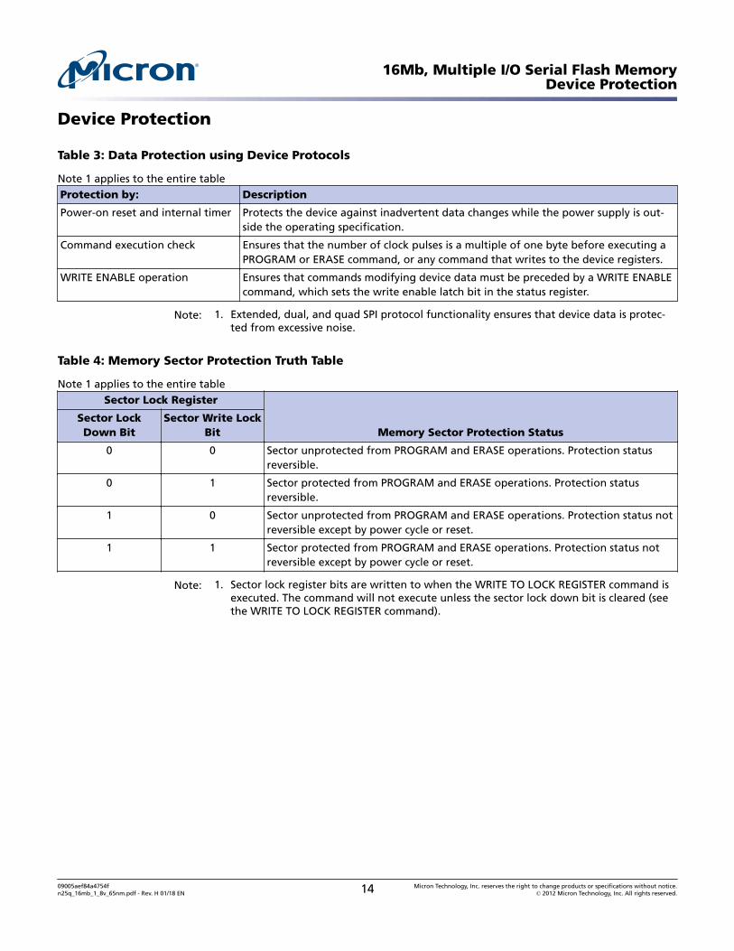
Device Protection
Table 3: Data Protection using Device Protocols
Note 1 applies to the entire tableProtection by: Description
Power-on reset and internal timer Protects the device against inadvertent data changes while the power supply is out-side the operating specification.
Command execution check Ensures that the number of clock pulses is a multiple of one byte before executing aPROGRAM or ERASE command, or any command that writes to the device registers.
WRITE ENABLE operation Ensures that commands modifying device data must be preceded by a WRITE ENABLEcommand, which sets the write enable latch bit in the status register.
Note: 1. Extended, dual, and quad SPI protocol functionality ensures that device data is protec-ted from excessive noise.
Table 4: Memory Sector Protection Truth Table
Note 1 applies to the entire tableSector Lock Register
Memory Sector Protection StatusSector LockDown Bit
Sector Write LockBit
0 0 Sector unprotected from PROGRAM and ERASE operations. Protection statusreversible.
0 1 Sector protected from PROGRAM and ERASE operations. Protection statusreversible.
1 0 Sector unprotected from PROGRAM and ERASE operations. Protection status notreversible except by power cycle or reset.
1 1 Sector protected from PROGRAM and ERASE operations. Protection status notreversible except by power cycle or reset.
Note: 1. Sector lock register bits are written to when the WRITE TO LOCK REGISTER command isexecuted. The command will not execute unless the sector lock down bit is cleared (seethe WRITE TO LOCK REGISTER command).
16Mb, Multiple I/O Serial Flash MemoryDevice Protection
09005aef84a4754fn25q_16mb_1_8v_65nm.pdf - Rev. H 01/18 EN 14 Micron Technology, Inc. reserves the right to change products or specifications without notice.
© 2012 Micron Technology, Inc. All rights reserved.
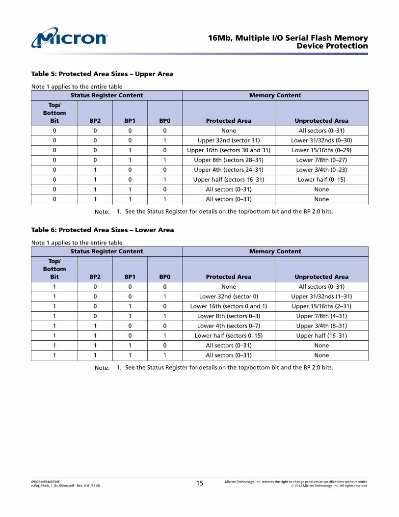
Table 5: Protected Area Sizes – Upper Area
Note 1 applies to the entire tableStatus Register Content Memory Content
Top/Bottom
Bit BP2 BP1 BP0 Protected Area Unprotected Area
0 0 0 0 None All sectors (0–31)
0 0 0 1 Upper 32nd (sector 31) Lower 31/32nds (0–30)
0 0 1 0 Upper 16th (sectors 30 and 31) Lower 15/16ths (0–29)
0 0 1 1 Upper 8th (sectors 28–31) Lower 7/8th (0–27)
0 1 0 0 Upper 4th (sectors 24–31) Lower 3/4th (0–23)
0 1 0 1 Upper half (sectors 16–31) Lower half (0–15)
0 1 1 0 All sectors (0–31) None
0 1 1 1 All sectors (0–31) None
Note: 1. See the Status Register for details on the top/bottom bit and the BP 2:0 bits.
Table 6: Protected Area Sizes – Lower Area
Note 1 applies to the entire tableStatus Register Content Memory Content
Top/Bottom
Bit BP2 BP1 BP0 Protected Area Unprotected Area
1 0 0 0 None All sectors (0–31)
1 0 0 1 Lower 32nd (sector 0) Upper 31/32nds (1–31)
1 0 1 0 Lower 16th (sectors 0 and 1) Upper 15/16ths (2–31)
1 0 1 1 Lower 8th (sectors 0–3) Upper 7/8th (4–31)
1 1 0 0 Lower 4th (sectors 0–7) Upper 3/4th (8–31)
1 1 0 1 Lower half (sectors 0–15) Upper half (16–31)
1 1 1 0 All sectors (0–31) None
1 1 1 1 All sectors (0–31) None
Note: 1. See the Status Register for details on the top/bottom bit and the BP 2:0 bits.
16Mb, Multiple I/O Serial Flash MemoryDevice Protection
09005aef84a4754fn25q_16mb_1_8v_65nm.pdf - Rev. H 01/18 EN 15 Micron Technology, Inc. reserves the right to change products or specifications without notice.
© 2012 Micron Technology, Inc. All rights reserved.
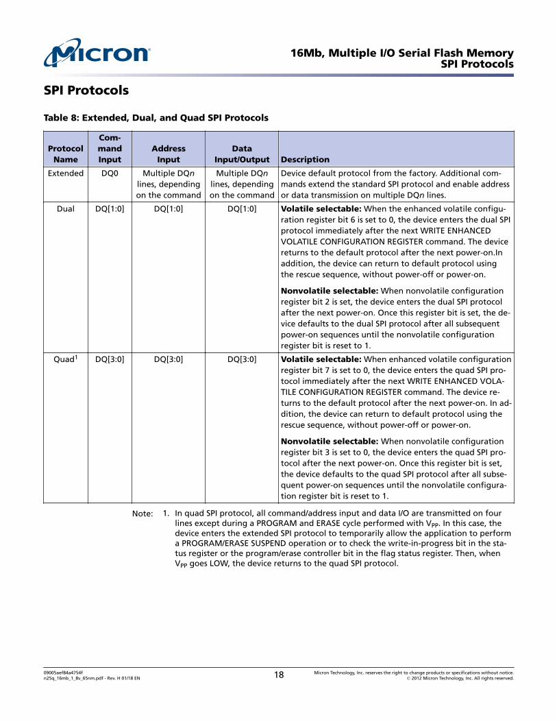
Serial Peripheral Interface ModesThe device can be driven by a microcontroller while its serial peripheral interface is ineither of the two modes shown here. The difference between the two modes is the clockpolarity when the bus master is in standby mode and not transferring data. Input data islatched in on the rising edge of the clock, and output data is available from the fallingedge of the clock.
Table 7: SPI Modes
Note 1 applies to the entire tableSPI Modes Clock Polarity
CPOL = 0, CPHA = 0 C remains at 0 for (CPOL = 0, CPHA = 0)
CPOL = 1, CPHA = 1 C remains at 1 for (CPOL = 1, CPHA = 1)
Note: 1. The listed SPI modes are supported in extended, dual, and quad SPI protocols.
Shown below is an example of three memory devices in extended SPI protocol in a sim-ple connection to an MCU on an SPI bus. Because only one device is selected at a time,that one device drives DQ1, while the other devices are High-Z.
Resistors ensure the device is not selected if the bus master leaves S# High-Z. The busmaster might enter a state in which all input/output is High-Z simultaneously, such aswhen the bus master is reset. Therefore, the serial clock must be connected to an exter-nal pull-down resistor so that S# is pulled HIGH while the serial clock is pulled LOW.This ensures that S# and the serial clock are not HIGH simultaneously and that tSHCHis met. The typical resistor value of 100kΩ, assuming that the time constant R × Cp (Cp =parasitic capacitance of the bus line), is shorter than the time the bus master leaves theSPI bus in High-Z.
Example: Cp = 50pF, that is R × Cp = 5μs. The application must ensure that the bus mas-ter never leaves the SPI bus High-Z for a time period shorter than 5μs. W# and HOLD#should be driven either HIGH or LOW, as appropriate.
16Mb, Multiple I/O Serial Flash MemorySerial Peripheral Interface Modes
09005aef84a4754fn25q_16mb_1_8v_65nm.pdf - Rev. H 01/18 EN 16 Micron Technology, Inc. reserves the right to change products or specifications without notice.
© 2012 Micron Technology, Inc. All rights reserved.
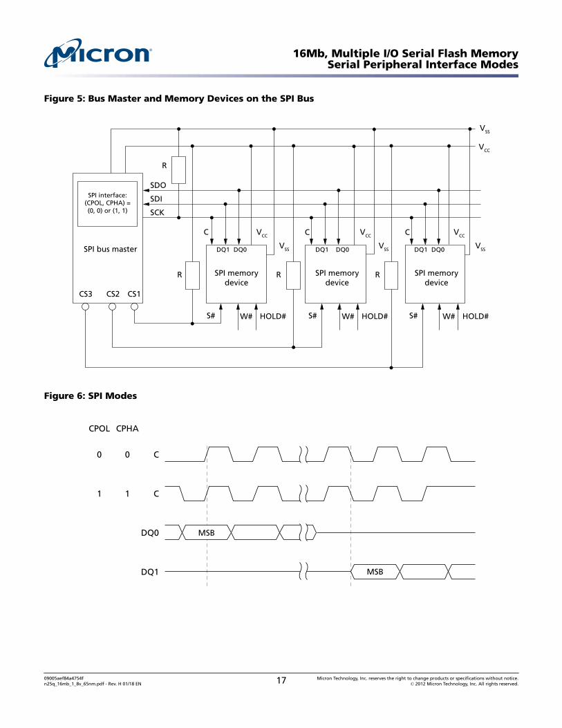
Figure 5: Bus Master and Memory Devices on the SPI Bus
SPI bus master
SPI memorydevice
SDO
SDI
SCK
C
DQ1 DQ0
SPI memorydevice
C
DQ1 DQ0
SPI memorydevice
C
DQ1 DQ0
S#
CS3 CS2 CS1
SPI interface:(CPOL, CPHA) =(0, 0) or (1, 1)
W# HOLD# S# W# HOLD# S# W# HOLD#
R R R
VCC
VCC VCC VCC
VSS
VSS VSS VSS
R
Figure 6: SPI Modes
C
C
DQ0
DQ1
CPHA
0
1
CPOL
0
1
MSB
MSB
16Mb, Multiple I/O Serial Flash MemorySerial Peripheral Interface Modes
09005aef84a4754fn25q_16mb_1_8v_65nm.pdf - Rev. H 01/18 EN 17 Micron Technology, Inc. reserves the right to change products or specifications without notice.
© 2012 Micron Technology, Inc. All rights reserved.
SPI Protocols
Table 8: Extended, Dual, and Quad SPI Protocols
ProtocolName
Com-mandInput
AddressInput
DataInput/Output Description
Extended DQ0 Multiple DQnlines, dependingon the command
Multiple DQnlines, dependingon the command
Device default protocol from the factory. Additional com-mands extend the standard SPI protocol and enable addressor data transmission on multiple DQn lines.
Dual DQ[1:0] DQ[1:0] DQ[1:0] Volatile selectable: When the enhanced volatile configu-ration register bit 6 is set to 0, the device enters the dual SPIprotocol immediately after the next WRITE ENHANCEDVOLATILE CONFIGURATION REGISTER command. The devicereturns to the default protocol after the next power-on.Inaddition, the device can return to default protocol usingthe rescue sequence, without power-off or power-on.
Nonvolatile selectable: When nonvolatile configurationregister bit 2 is set, the device enters the dual SPI protocolafter the next power-on. Once this register bit is set, the de-vice defaults to the dual SPI protocol after all subsequentpower-on sequences until the nonvolatile configurationregister bit is reset to 1.
Quad1 DQ[3:0] DQ[3:0] DQ[3:0] Volatile selectable: When enhanced volatile configurationregister bit 7 is set to 0, the device enters the quad SPI pro-tocol immediately after the next WRITE ENHANCED VOLA-TILE CONFIGURATION REGISTER command. The device re-turns to the default protocol after the next power-on. In ad-dition, the device can return to default protocol using therescue sequence, without power-off or power-on.
Nonvolatile selectable: When nonvolatile configurationregister bit 3 is set to 0, the device enters the quad SPI pro-tocol after the next power-on. Once this register bit is set,the device defaults to the quad SPI protocol after all subse-quent power-on sequences until the nonvolatile configura-tion register bit is reset to 1.
Note: 1. In quad SPI protocol, all command/address input and data I/O are transmitted on fourlines except during a PROGRAM and ERASE cycle performed with VPP. In this case, thedevice enters the extended SPI protocol to temporarily allow the application to performa PROGRAM/ERASE SUSPEND operation or to check the write-in-progress bit in the sta-tus register or the program/erase controller bit in the flag status register. Then, whenVPP goes LOW, the device returns to the quad SPI protocol.
16Mb, Multiple I/O Serial Flash MemorySPI Protocols
09005aef84a4754fn25q_16mb_1_8v_65nm.pdf - Rev. H 01/18 EN 18 Micron Technology, Inc. reserves the right to change products or specifications without notice.
© 2012 Micron Technology, Inc. All rights reserved.
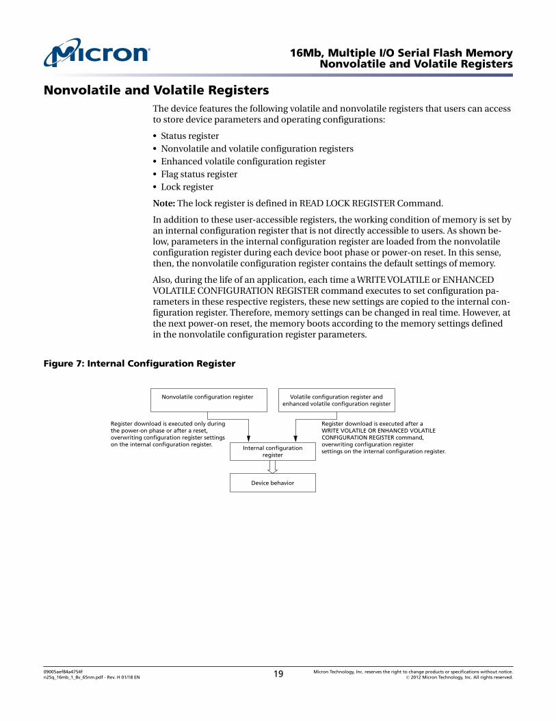
Nonvolatile and Volatile RegistersThe device features the following volatile and nonvolatile registers that users can accessto store device parameters and operating configurations:
• Status register• Nonvolatile and volatile configuration registers• Enhanced volatile configuration register• Flag status register• Lock register
Note: The lock register is defined in READ LOCK REGISTER Command.
In addition to these user-accessible registers, the working condition of memory is set byan internal configuration register that is not directly accessible to users. As shown be-low, parameters in the internal configuration register are loaded from the nonvolatileconfiguration register during each device boot phase or power-on reset. In this sense,then, the nonvolatile configuration register contains the default settings of memory.
Also, during the life of an application, each time a WRITE VOLATILE or ENHANCEDVOLATILE CONFIGURATION REGISTER command executes to set configuration pa-rameters in these respective registers, these new settings are copied to the internal con-figuration register. Therefore, memory settings can be changed in real time. However, atthe next power-on reset, the memory boots according to the memory settings definedin the nonvolatile configuration register parameters.
Figure 7: Internal Configuration Register
Register download is executed only duringthe power-on phase or after a reset,overwriting configuration register settingson the internal configuration register.
Register download is executed after aWRITE VOLATILE OR ENHANCED VOLATILECONFIGURATION REGISTER command,overwriting configuration registersettings on the internal configuration register.
Nonvolatile configuration register
Internal configurationregister
Device behavior
Volatile configuration register andenhanced volatile configuration register
16Mb, Multiple I/O Serial Flash MemoryNonvolatile and Volatile Registers
09005aef84a4754fn25q_16mb_1_8v_65nm.pdf - Rev. H 01/18 EN 19 Micron Technology, Inc. reserves the right to change products or specifications without notice.
© 2012 Micron Technology, Inc. All rights reserved.
Status Register
Table 9: Status Register Bit Definitions
Note 1 applies to entire tableBit Name Settings Description Notes
7 Status registerwrite enable/disable
0 = Enabled1 = Disabled
Nonvolatile bit: Used with the W/VPP signal to enable ordisable writing to the status register.
3
6 Reserved 0 Reserved
5 Top/bottom 0 = Top1 = Bottom
Nonvolatile bit: Determines whether the protected mem-ory area defined by the block protect bits starts from thetop or bottom of the memory array.
4
4:2 Block protect 2–0 See Protected AreaSizes – Upper Areaand Lower Areatables in DeviceProtection
Nonvolatile bit: Defines memory to be software protec-ted against PROGRAM or ERASE operations. When one ormore block protect bits is set to 1, a designated memoryarea is protected from PROGRAM and ERASE operations.
4
1 Write enable latch 0 = Cleared (Default)1 = Set
Volatile bit: The device always powers up with this bitcleared to prevent inadvertent WRITE STATUS REGISTER,PROGRAM, or ERASE operations. To enable these opera-tions, the WRITE ENABLE operation must be executed firstto set this bit.
2
0 Write in progress 0 = Ready1 = Busy
Volatile bit: Indicates if one of the following command cy-cles is in progress:WRITE STATUS REGISTERWRITE NONVOLATILE CONFIGURATION REGISTERPROGRAMERASE
2
Notes: 1. Bits can be read from or written to using READ STATUS REGISTER or WRITE STATUS REG-ISTER commands, respectively.
2. Volatile bits are cleared to 0 by a power cycle or reset.3. The status register write enable/disable bit, combined with the W#/VPP signal as descri-
bed in the Signal Descriptions, provides hardware data protection for the device as fol-lows: When the enable/disable bit is set to 1, and the W#/VPP signal is driven LOW, thestatus register nonvolatile bits become read-only and the WRITE STATUS REGISTER oper-ation will not execute. The only way to exit this hardware-protected mode is to driveW#/VPP HIGH.
4. See Protected Area Sizes tables in Device Protection. The BULK ERASE command is exe-cuted only if all bits are 0.
16Mb, Multiple I/O Serial Flash MemoryNonvolatile and Volatile Registers
09005aef84a4754fn25q_16mb_1_8v_65nm.pdf - Rev. H 01/18 EN 20 Micron Technology, Inc. reserves the right to change products or specifications without notice.
© 2012 Micron Technology, Inc. All rights reserved.
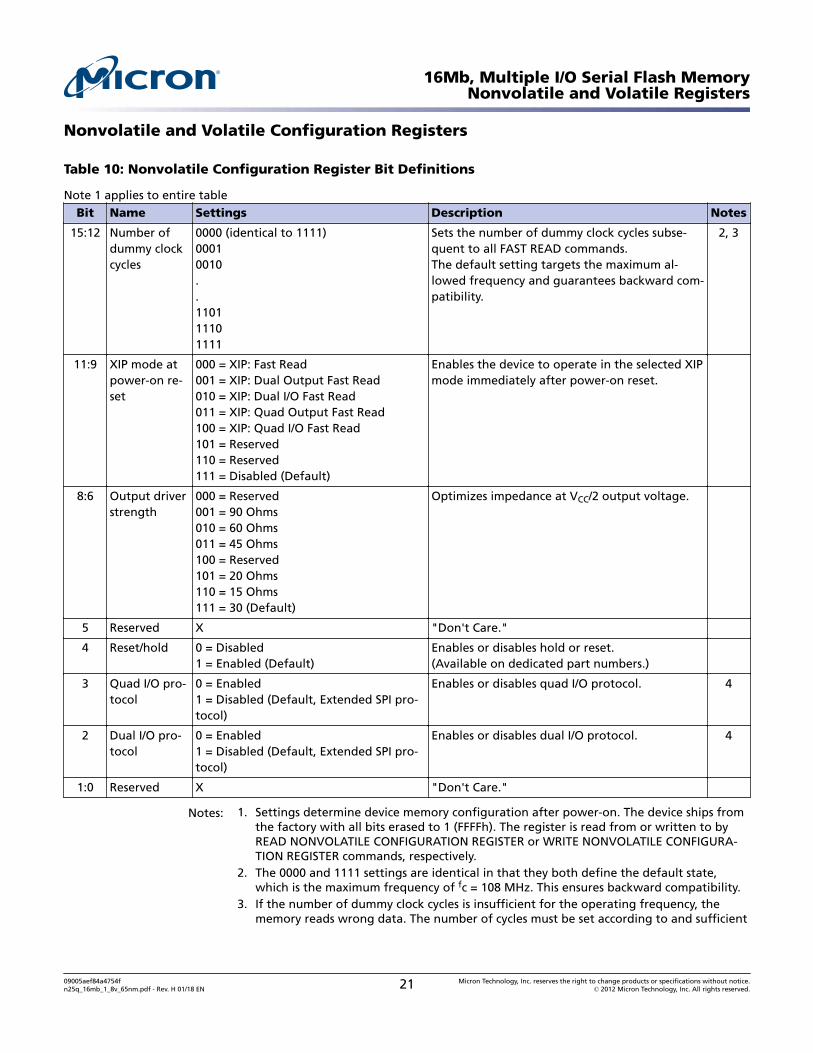
Nonvolatile and Volatile Configuration Registers
Table 10: Nonvolatile Configuration Register Bit Definitions
Note 1 applies to entire tableBit Name Settings Description Notes
15:12 Number ofdummy clockcycles
0000 (identical to 1111)00010010..110111101111
Sets the number of dummy clock cycles subse-quent to all FAST READ commands.The default setting targets the maximum al-lowed frequency and guarantees backward com-patibility.
2, 3
11:9 XIP mode atpower-on re-set
000 = XIP: Fast Read001 = XIP: Dual Output Fast Read010 = XIP: Dual I/O Fast Read011 = XIP: Quad Output Fast Read100 = XIP: Quad I/O Fast Read101 = Reserved110 = Reserved111 = Disabled (Default)
Enables the device to operate in the selected XIPmode immediately after power-on reset.
8:6 Output driverstrength
000 = Reserved001 = 90 Ohms010 = 60 Ohms011 = 45 Ohms100 = Reserved101 = 20 Ohms110 = 15 Ohms111 = 30 (Default)
Optimizes impedance at VCC/2 output voltage.
5 Reserved X "Don't Care."
4 Reset/hold 0 = Disabled1 = Enabled (Default)
Enables or disables hold or reset.(Available on dedicated part numbers.)
3 Quad I/O pro-tocol
0 = Enabled1 = Disabled (Default, Extended SPI pro-tocol)
Enables or disables quad I/O protocol. 4
2 Dual I/O pro-tocol
0 = Enabled1 = Disabled (Default, Extended SPI pro-tocol)
Enables or disables dual I/O protocol. 4
1:0 Reserved X "Don't Care."
Notes: 1. Settings determine device memory configuration after power-on. The device ships fromthe factory with all bits erased to 1 (FFFFh). The register is read from or written to byREAD NONVOLATILE CONFIGURATION REGISTER or WRITE NONVOLATILE CONFIGURA-TION REGISTER commands, respectively.
2. The 0000 and 1111 settings are identical in that they both define the default state,which is the maximum frequency of fc = 108 MHz. This ensures backward compatibility.
3. If the number of dummy clock cycles is insufficient for the operating frequency, thememory reads wrong data. The number of cycles must be set according to and sufficient
16Mb, Multiple I/O Serial Flash MemoryNonvolatile and Volatile Registers
09005aef84a4754fn25q_16mb_1_8v_65nm.pdf - Rev. H 01/18 EN 21 Micron Technology, Inc. reserves the right to change products or specifications without notice.
© 2012 Micron Technology, Inc. All rights reserved.
for the clock frequency, which varies by the type of FAST READ command, as shown inthe Supported Clock Frequencies table.
4. If bits 2 and 3 are both set to 0, the device operates in quad I/O. When bits 2 or 3 arereset to 0, the device operates in dual I/O or quad I/O respectively, after the next power-on.
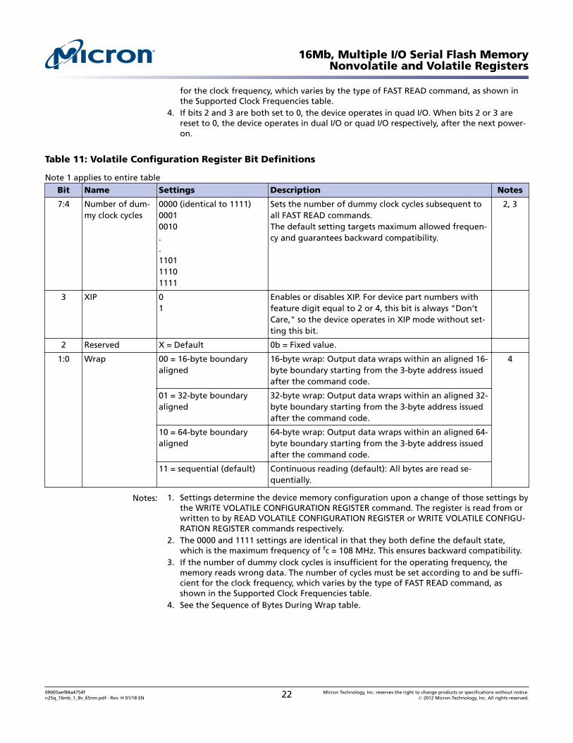
Table 11: Volatile Configuration Register Bit Definitions
Note 1 applies to entire tableBit Name Settings Description Notes
7:4 Number of dum-my clock cycles
0000 (identical to 1111)00010010..110111101111
Sets the number of dummy clock cycles subsequent toall FAST READ commands.The default setting targets maximum allowed frequen-cy and guarantees backward compatibility.
2, 3
3 XIP 01
Enables or disables XIP. For device part numbers withfeature digit equal to 2 or 4, this bit is always "Don’tCare," so the device operates in XIP mode without set-ting this bit.
2 Reserved X = Default 0b = Fixed value.
1:0 Wrap 00 = 16-byte boundaryaligned
16-byte wrap: Output data wraps within an aligned 16-byte boundary starting from the 3-byte address issuedafter the command code.
4
01 = 32-byte boundaryaligned
32-byte wrap: Output data wraps within an aligned 32-byte boundary starting from the 3-byte address issuedafter the command code.
10 = 64-byte boundaryaligned
64-byte wrap: Output data wraps within an aligned 64-byte boundary starting from the 3-byte address issuedafter the command code.
11 = sequential (default) Continuous reading (default): All bytes are read se-quentially.
Notes: 1. Settings determine the device memory configuration upon a change of those settings bythe WRITE VOLATILE CONFIGURATION REGISTER command. The register is read from orwritten to by READ VOLATILE CONFIGURATION REGISTER or WRITE VOLATILE CONFIGU-RATION REGISTER commands respectively.
2. The 0000 and 1111 settings are identical in that they both define the default state,which is the maximum frequency of fc = 108 MHz. This ensures backward compatibility.
3. If the number of dummy clock cycles is insufficient for the operating frequency, thememory reads wrong data. The number of cycles must be set according to and be suffi-cient for the clock frequency, which varies by the type of FAST READ command, asshown in the Supported Clock Frequencies table.
4. See the Sequence of Bytes During Wrap table.
16Mb, Multiple I/O Serial Flash MemoryNonvolatile and Volatile Registers
09005aef84a4754fn25q_16mb_1_8v_65nm.pdf - Rev. H 01/18 EN 22 Micron Technology, Inc. reserves the right to change products or specifications without notice.
© 2012 Micron Technology, Inc. All rights reserved.
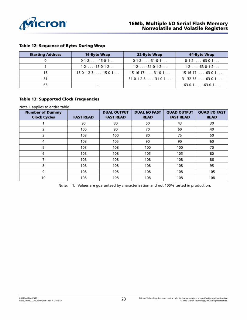
Table 12: Sequence of Bytes During Wrap
Starting Address 16-Byte Wrap 32-Byte Wrap 64-Byte Wrap
0 0-1-2- . . . -15-0-1- . . 0-1-2- . . . -31-0-1- . . 0-1-2- . . . -63-0-1- . .
1 1-2- . . . -15-0-1-2- . . 1-2- . . . -31-0-1-2- . . 1-2- . . . -63-0-1-2- . .
15 15-0-1-2-3- . . . -15-0-1- . . 15-16-17- . . . -31-0-1- . . 15-16-17- . . . -63-0-1- . .
31 – 31-0-1-2-3- . . . -31-0-1- . . 31-32-33- . . . -63-0-1- . .
63 – – 63-0-1- . . . -63-0-1- . .
Table 13: Supported Clock Frequencies
Note 1 applies to entire tableNumber of Dummy
Clock Cycles FAST READDUAL OUTPUT
FAST READDUAL I/O FAST
READQUAD OUTPUT
FAST READQUAD I/O FAST
READ
1 90 80 50 43 30
2 100 90 70 60 40
3 108 100 80 75 50
4 108 105 90 90 60
5 108 108 100 100 70
6 108 108 105 105 80
7 108 108 108 108 86
8 108 108 108 108 95
9 108 108 108 108 105
10 108 108 108 108 108
Note: 1. Values are guaranteed by characterization and not 100% tested in production.
16Mb, Multiple I/O Serial Flash MemoryNonvolatile and Volatile Registers
09005aef84a4754fn25q_16mb_1_8v_65nm.pdf - Rev. H 01/18 EN 23 Micron Technology, Inc. reserves the right to change products or specifications without notice.
© 2012 Micron Technology, Inc. All rights reserved.
Enhanced Volatile Configuration Register
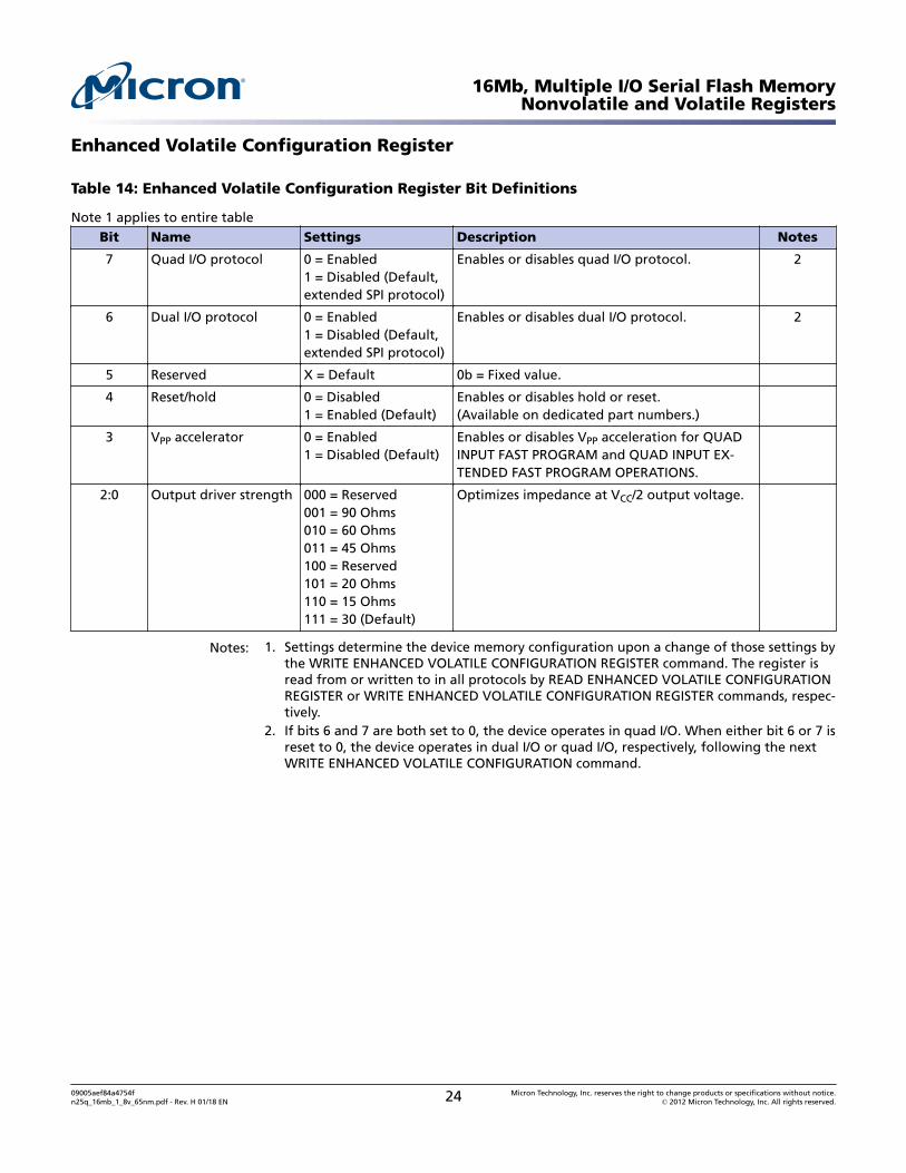
Table 14: Enhanced Volatile Configuration Register Bit Definitions
Note 1 applies to entire tableBit Name Settings Description Notes
7 Quad I/O protocol 0 = Enabled1 = Disabled (Default,extended SPI protocol)
Enables or disables quad I/O protocol. 2
6 Dual I/O protocol 0 = Enabled1 = Disabled (Default,extended SPI protocol)
Enables or disables dual I/O protocol. 2
5 Reserved X = Default 0b = Fixed value.
4 Reset/hold 0 = Disabled1 = Enabled (Default)
Enables or disables hold or reset.(Available on dedicated part numbers.)
3 VPP accelerator 0 = Enabled1 = Disabled (Default)
Enables or disables VPP acceleration for QUADINPUT FAST PROGRAM and QUAD INPUT EX-TENDED FAST PROGRAM OPERATIONS.
2:0 Output driver strength 000 = Reserved001 = 90 Ohms010 = 60 Ohms011 = 45 Ohms100 = Reserved101 = 20 Ohms110 = 15 Ohms111 = 30 (Default)
Optimizes impedance at VCC/2 output voltage.
Notes: 1. Settings determine the device memory configuration upon a change of those settings bythe WRITE ENHANCED VOLATILE CONFIGURATION REGISTER command. The register isread from or written to in all protocols by READ ENHANCED VOLATILE CONFIGURATIONREGISTER or WRITE ENHANCED VOLATILE CONFIGURATION REGISTER commands, respec-tively.
2. If bits 6 and 7 are both set to 0, the device operates in quad I/O. When either bit 6 or 7 isreset to 0, the device operates in dual I/O or quad I/O, respectively, following the nextWRITE ENHANCED VOLATILE CONFIGURATION command.
16Mb, Multiple I/O Serial Flash MemoryNonvolatile and Volatile Registers
09005aef84a4754fn25q_16mb_1_8v_65nm.pdf - Rev. H 01/18 EN 24 Micron Technology, Inc. reserves the right to change products or specifications without notice.
© 2012 Micron Technology, Inc. All rights reserved.
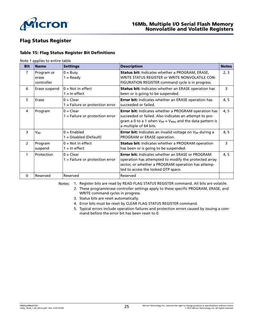
Flag Status Register
Table 15: Flag Status Register Bit Definitions
Note 1 applies to entire tableBit Name Settings Description Notes
7 Program orerasecontroller
0 = Busy1 = Ready
Status bit: Indicates whether a PROGRAM, ERASE,WRITE STATUS REGISTER or WRITE NONVOLATILE CON-FIGURATION REGISTER command cycle is in progress.
2, 3
6 Erase suspend 0 = Not in effect1 = In effect
Status bit: Indicates whether an ERASE operation hasbeen or is going to be suspended.
3
5 Erase 0 = Clear1 = Failure or protection error
Error bit: Indicates whether an ERASE operation hassucceeded or failed.
4, 5
4 Program 0 = Clear1 = Failure or protection error
Error bit: Indicates whether a PROGRAM operation hassucceeded or failed. Also indicates an attempt to pro-gram a 0 to a 1 when VPP = VPPH and the data pattern isa multiple of 64 bits.
4, 5
3 VPP 0 = Enabled1 = Disabled (Default)
Error bit: Indicates an invalid voltage on VPP during aPROGRAM or ERASE operation.
4, 5
2 Programsuspend
0 = Not in effect1 = In effect
Status bit: Indicates whether a PROGRAM operationhas been or is going to be suspended.
3
1 Protection 0 = Clear1 = Failure or protection error
Error bit: Indicates whether an ERASE or PROGRAMoperation has attempted to modify the protected arraysector, or whether a PROGRAM operation has attemp-ted to access the locked OTP space.
4, 5
0 Reserved Reserved Reserved
Notes: 1. Register bits are read by READ FLAG STATUS REGISTER command. All bits are volatile.2. These program/erase controller settings apply to these specific PROGRAM, ERASE, and
WRITE command cycles in progress.3. Status bits are reset automatically.4. Error bits must be reset by CLEAR FLAG STATUS REGISTER command.5. Typical errors include operation failures and protection errors caused by issuing a com-
mand before the error bit has been reset to 0.
16Mb, Multiple I/O Serial Flash MemoryNonvolatile and Volatile Registers
09005aef84a4754fn25q_16mb_1_8v_65nm.pdf - Rev. H 01/18 EN 25 Micron Technology, Inc. reserves the right to change products or specifications without notice.
© 2012 Micron Technology, Inc. All rights reserved.
Command Definitions
Table 16: Command Set
Note 1 applies to entire table
Command Code ExtendedDualI/O
QuadI/O
DataBytes Notes
RESET Operations
RESET ENABLE 66h Yes Yes Yes 0 2
RESET MEMORY 99h
IDENTIFICATION Operations
READ ID 9E/9Fh Yes No No 1 to 20 2
MULTIPLE INPUT/OUTPUT READ ID AFh No Yes Yes 1 to 3 2
READ SERIAL FLASHDISCOVERY PARAMETER
5Ah Yes Yes Yes 1 to ∞ 3
READ Operations
READ 03h Yes No No 1 to ∞ 4
FAST READ 0Bh Yes Yes Yes 5
DUAL OUTPUT FAST READ 3Bh Yes Yes No 1 to ∞ 5
DUAL INPUT/OUTPUT FAST READ 0Bh3BhBBh
Yes Yes No 5, 6
QUAD OUTPUT FAST READ 6Bh Yes No Yes 1 to ∞ 5
QUAD INPUT/OUTPUT FAST READ 0Bh6BhEBh
Yes No Yes 5, 7
WRITE Operations
WRITE ENABLE 06h Yes Yes Yes 0 2
WRITE DISABLE 04h
REGISTER Operations
READ STATUS REGISTER 05h Yes Yes Yes 1 to ∞ 2
WRITE STATUS REGISTER 01h 1 2, 8
READ LOCK REGISTER E8h Yes Yes Yes 1 to ∞ 4
WRITE LOCK REGISTER E5h 1 4, 8
READ FLAG STATUS REGISTER 70h Yes Yes Yes 1 to ∞ 2
CLEAR FLAG STATUS REGISTER 50h 0
READ NONVOLATILECONFIGURATION REGISTER
B5h Yes Yes Yes 2 2
WRITE NONVOLATILECONFIGURATION REGISTER
B1h 2, 8
READ VOLATILECONFIGURATION REGISTER
85h Yes Yes Yes 1 to ∞ 2
WRITE VOLATILECONFIGURATION REGISTER
81h 1 2, 8
16Mb, Multiple I/O Serial Flash MemoryCommand Definitions
09005aef84a4754fn25q_16mb_1_8v_65nm.pdf - Rev. H 01/18 EN 26 Micron Technology, Inc. reserves the right to change products or specifications without notice.
© 2012 Micron Technology, Inc. All rights reserved.
Table 16: Command Set (Continued)
Note 1 applies to entire table
Command Code ExtendedDualI/O
QuadI/O
DataBytes Notes
READ ENHANCEDVOLATILE CONFIGURATIONREGISTER
65h Yes Yes Yes 1 to ∞ 2
WRITE ENHANCEDVOLATILE CONFIGURATIONREGISTER
61h 1 2, 8
PROGRAM Operations
PAGE PROGRAM 02h Yes Yes Yes 1 to 256 4, 8
DUAL INPUT FAST PROGRAM A2h Yes Yes No 1 to 256 4, 8
EXTENDED DUAL INPUTFAST PROGRAM
02hA2hD2h
Yes Yes No 4, 6, 8
QUAD INPUT FAST PROGRAM 32h Yes No Yes 1 to 256 4, 8
EXTENDED QUAD INPUTFAST PROGRAM
02h32h12h
Yes No Yes 4, 7, 8
ERASE Operations
SUBSECTOR ERASE (4KB) 20h Yes Yes Yes 0 4, 8
SUBSECTOR ERASE (32KB) 52h
SECTOR ERASE D8h
BULK ERASE C7h 2, 8
PROGRAM/ERASE RESUME 7Ah Yes Yes Yes 0 2, 8
PROGRAM/ERASE SUSPEND 75h
ONE-TIME PROGRAMMABLE (OTP) Operations
READ OTP ARRAY 4Bh Yes Yes Yes 1 to 64 5
PROGRAM OTP ARRAY 42h 4
Power-Down
Deep power-down B9h Yes Yes Yes 0 2
Release from deep power-down ABh
Notes: 1. Yes in the protocol columns indicates that the command is supported and has the samefunctionality and command sequence as other commands marked Yes.
2. Address bytes = 0. Dummy clock cycles = 0.3. Dummy clock cycles default = 8.4. Address bytes = 3. Dummy clock cycles = 0.5. Address bytes = 3. Dummy clock cycles default = 8. Dummy clock cycles default = 10
(when quad SPI protocol is enabled). Dummy clock cycles is configurable by the user.6. When the device is in dual SPI protocol, the command can be entered with any of the
three dual FAST READ or dual PROGRAM codes. The different codes enable compatibili-ty between dual SPI and extended SPI protocols.
16Mb, Multiple I/O Serial Flash MemoryCommand Definitions
09005aef84a4754fn25q_16mb_1_8v_65nm.pdf - Rev. H 01/18 EN 27 Micron Technology, Inc. reserves the right to change products or specifications without notice.
© 2012 Micron Technology, Inc. All rights reserved.
7. When the device is in quad SPI protocol, the command can be entered with any of thethree quad FAST READ or quad PROGRAM codes. The different codes enable compatibil-ity between quad SPI and extended SPI protocols.
8. The WRITE ENABLE command must be issued first before this command can be execu-ted.
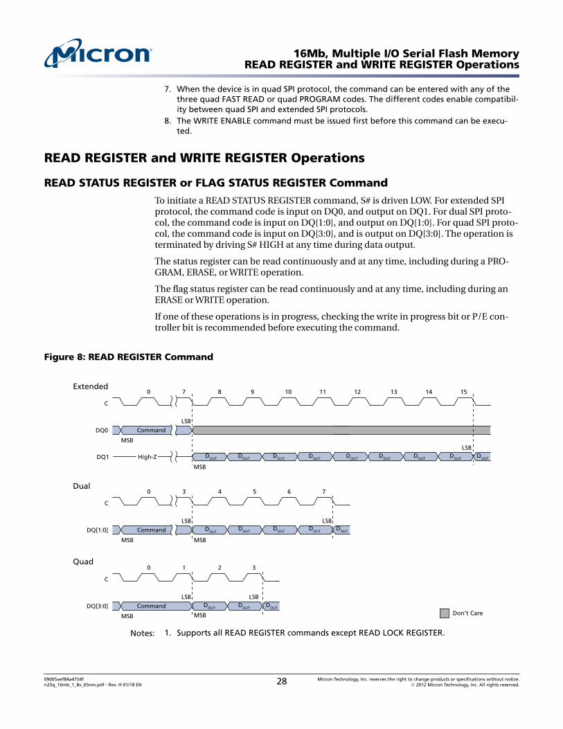
READ REGISTER and WRITE REGISTER Operations
READ STATUS REGISTER or FLAG STATUS REGISTER Command
To initiate a READ STATUS REGISTER command, S# is driven LOW. For extended SPIprotocol, the command code is input on DQ0, and output on DQ1. For dual SPI proto-col, the command code is input on DQ[1:0], and output on DQ[1:0]. For quad SPI proto-col, the command code is input on DQ[3:0], and is output on DQ[3:0]. The operation isterminated by driving S# HIGH at any time during data output.
The status register can be read continuously and at any time, including during a PRO-GRAM, ERASE, or WRITE operation.
The flag status register can be read continuously and at any time, including during anERASE or WRITE operation.
If one of these operations is in progress, checking the write in progress bit or P/E con-troller bit is recommended before executing the command.
Figure 8: READ REGISTER Command
High-ZDQ1
7 8 9 10 11 12 13 14 150
C
MSB
DQ0
LSB
Command
3 4 5 6 70
C
MSB
DQ[1:0]
LSB
Command
MSB
DOUTDOUT DOUT DOUT DOUT
LSB
Extended
MSB
DOUT DOUT DOUT DOUT DOUT
LSBDOUT DOUT DOUT DOUT
Dual
Quad1 2 30
C
MSB
DQ[3:0]
LSB
Command
MSB
DOUT DOUT DOUT
LSB
Don’t Care
Notes: 1. Supports all READ REGISTER commands except READ LOCK REGISTER.
16Mb, Multiple I/O Serial Flash MemoryREAD REGISTER and WRITE REGISTER Operations
09005aef84a4754fn25q_16mb_1_8v_65nm.pdf - Rev. H 01/18 EN 28 Micron Technology, Inc. reserves the right to change products or specifications without notice.
© 2012 Micron Technology, Inc. All rights reserved.
2. A READ NONVOLATILE CONFIGURATION REGISTER operation will output data startingfrom the least significant byte.
READ NONVOLATILE CONFIGURATION REGISTER Command
To execute a READ NONVOLATILE CONFIGURATION REGISTER command, S# is driv-en LOW. For extended SPI protocol, the command code is input on DQ0, and output onDQ1. For dual SPI protocol, the command code is input on DQ[1:0], and output onDQ[1:0]. For quad SPI protocol, the command code is input on DQ[3:0], and is outputon DQ[3:0]. The operation is terminated by driving S# HIGH at any time during dataoutput.
The nonvolatile configuration register can be read continuously. After all 16 bits of theregister have been read, a 0 is output. All reserved fields output a value of 1.
READ VOLATILE or ENHANCED VOLATILE CONFIGURATION REGISTER Command
To execute a READ VOLATILE CONFIGURATION REGISTER command or a READ EN-HANCED VOLATILE CONFIGURATION REGISTER command, S# is driven LOW. For ex-tended SPI protocol, the command code is input on DQ0, and output on DQ1. For dualSPI protocol, the command code is input on DQ[1:0], and output on DQ[1:0]. For quadSPI protocol, the command code is input on DQ[3:0], and is output on DQ[3:0]. The op-eration is terminated by driving S# HIGH at any time during data output.
When the register is read continuously, the same byte is output repeatedly.
WRITE STATUS REGISTER Command
To issue a WRITE STATUS REGISTER command, the WRITE ENABLE command must beexecuted to set the write enable latch bit to 1. S# is driven LOW and held LOW until theeighth bit of the last data byte has been latched in, after which it must be driven HIGH.For extended SPI protocol, the command code is input on DQ0, followed by the databytes. For dual SPI protocol, the command code is input on DQ[1:0], followed by the da-ta bytes. For quad SPI protocol, the command code is input on DQ[3:0], followed by thedata bytes. When S# is driven HIGH, the operation, which is self-timed, is initiated; itsduration is tW.
This command is used to write new values to status register bits 7:2, enabling softwaredata protection. The status register can also be combined with the W# signal to providehardware data protection. The WRITE STATUS REGISTER command has no effect onstatus register bits 1:0.
When the operation is in progress, the write in progress bit is set to 1. The write enablelatch bit is cleared to 0, whether the operation is successful or not. The status registerand flag status register can be polled for the operation status. When the operation com-pletes, the write in progress bit is cleared to 0, whether the operation is successful ornot.
16Mb, Multiple I/O Serial Flash MemoryREAD REGISTER and WRITE REGISTER Operations
09005aef84a4754fn25q_16mb_1_8v_65nm.pdf - Rev. H 01/18 EN 29 Micron Technology, Inc. reserves the right to change products or specifications without notice.
© 2012 Micron Technology, Inc. All rights reserved.
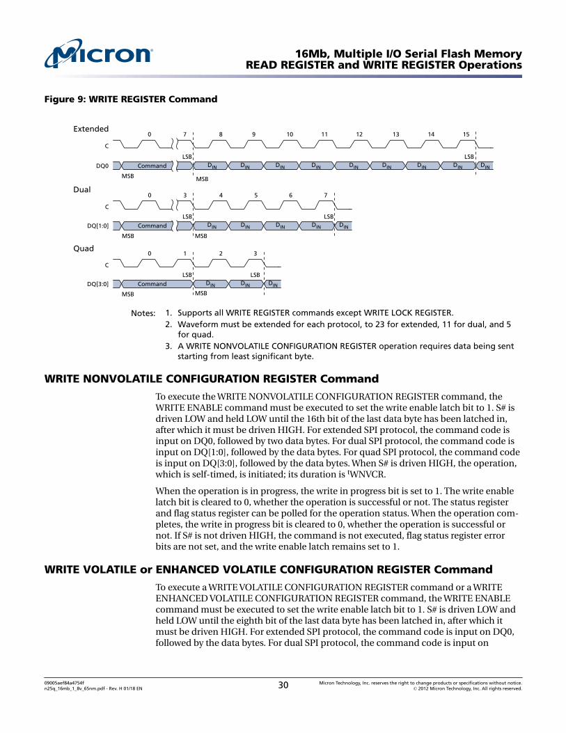
Figure 9: WRITE REGISTER Command
7 8 9 10 11 12 13 14 150
C
MSB
DQ0
LSB
Command
3 4 5 6 70
C
MSB
DQ[1:0]
LSB
Command
MSB
DIN DIN DIN DIN DIN
LSB
Extended
MSB
LSBDIN DIN DIN DIN DINDIN DIN DIN DIN
Dual
Quad1 2 30
C
MSB
DQ[3:0]
LSB
Command
MSB
DIN DIN DIN
LSB
Notes: 1. Supports all WRITE REGISTER commands except WRITE LOCK REGISTER.2. Waveform must be extended for each protocol, to 23 for extended, 11 for dual, and 5
for quad.3. A WRITE NONVOLATILE CONFIGURATION REGISTER operation requires data being sent
starting from least significant byte.
WRITE NONVOLATILE CONFIGURATION REGISTER Command
To execute the WRITE NONVOLATILE CONFIGURATION REGISTER command, theWRITE ENABLE command must be executed to set the write enable latch bit to 1. S# isdriven LOW and held LOW until the 16th bit of the last data byte has been latched in,after which it must be driven HIGH. For extended SPI protocol, the command code isinput on DQ0, followed by two data bytes. For dual SPI protocol, the command code isinput on DQ[1:0], followed by the data bytes. For quad SPI protocol, the command codeis input on DQ[3:0], followed by the data bytes. When S# is driven HIGH, the operation,which is self-timed, is initiated; its duration is tWNVCR.
When the operation is in progress, the write in progress bit is set to 1. The write enablelatch bit is cleared to 0, whether the operation is successful or not. The status registerand flag status register can be polled for the operation status. When the operation com-pletes, the write in progress bit is cleared to 0, whether the operation is successful ornot. If S# is not driven HIGH, the command is not executed, flag status register errorbits are not set, and the write enable latch remains set to 1.
WRITE VOLATILE or ENHANCED VOLATILE CONFIGURATION REGISTER Command
To execute a WRITE VOLATILE CONFIGURATION REGISTER command or a WRITEENHANCED VOLATILE CONFIGURATION REGISTER command, the WRITE ENABLEcommand must be executed to set the write enable latch bit to 1. S# is driven LOW andheld LOW until the eighth bit of the last data byte has been latched in, after which itmust be driven HIGH. For extended SPI protocol, the command code is input on DQ0,followed by the data bytes. For dual SPI protocol, the command code is input on
16Mb, Multiple I/O Serial Flash MemoryREAD REGISTER and WRITE REGISTER Operations
09005aef84a4754fn25q_16mb_1_8v_65nm.pdf - Rev. H 01/18 EN 30 Micron Technology, Inc. reserves the right to change products or specifications without notice.
© 2012 Micron Technology, Inc. All rights reserved.
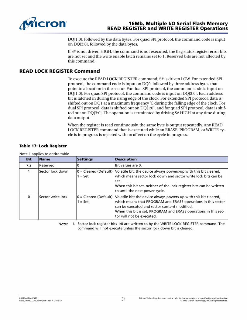
DQ[1:0], followed by the data bytes. For quad SPI protocol, the command code is inputon DQ[3:0], followed by the data bytes.
If S# is not driven HIGH, the command is not executed, the flag status register error bitsare not set and the write enable latch remains set to 1. Reserved bits are not affected bythis command.
READ LOCK REGISTER Command
To execute the READ LOCK REGISTER command, S# is driven LOW. For extended SPIprotocol, the command code is input on DQ0, followed by three address bytes thatpoint to a location in the sector. For dual SPI protocol, the command code is input onDQ[1:0]. For quad SPI protocol, the command code is input on DQ[3:0]. Each addressbit is latched in during the rising edge of the clock. For extended SPI protocol, data isshifted out on DQ1 at a maximum frequency fC during the falling edge of the clock. Fordual SPI protocol, data is shifted out on DQ[1:0], and for quad SPI protocol, data is shif-ted out on DQ[3:0]. The operation is terminated by driving S# HIGH at any time duringdata output.
When the register is read continuously, the same byte is output repeatedly. Any READLOCK REGISTER command that is executed while an ERASE, PROGRAM, or WRITE cy-cle is in progress is rejected with no affect on the cycle in progress.
Table 17: Lock Register
Note 1 applies to entire tableBit Name Settings Description
7:2 Reserved 0 Bit values are 0.
1 Sector lock down 0 = Cleared (Default)1 = Set
Volatile bit: the device always powers-up with this bit cleared,which means sector lock down and sector write lock bits can beset.When this bit set, neither of the lock register bits can be writtento until the next power cycle.
0 Sector write lock 0 = Cleared (Default)1 = Set
Volatile bit: the device always powers-up with this bit cleared,which means that PROGRAM and ERASE operations in this sectorcan be executed and sector content modified.When this bit is set, PROGRAM and ERASE operations in this sec-tor will not be executed.
Note: 1. Sector lock register bits 1:0 are written to by the WRITE LOCK REGISTER command. Thecommand will not execute unless the sector lock down bit is cleared.
16Mb, Multiple I/O Serial Flash MemoryREAD REGISTER and WRITE REGISTER Operations
09005aef84a4754fn25q_16mb_1_8v_65nm.pdf - Rev. H 01/18 EN 31 Micron Technology, Inc. reserves the right to change products or specifications without notice.
© 2012 Micron Technology, Inc. All rights reserved.
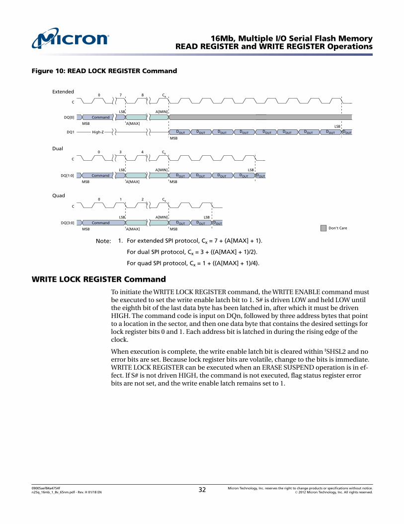
Figure 10: READ LOCK REGISTER Command
MSB
DQ[0]
LSB
Command
A[MAX]
A[MIN]
7 8 Cx0
C
3 4 Cx0
C
MSB
DQ[1:0]
LSB
Command
A[MAX]
A[MIN]
MSB
DOUT DOUT DOUT DOUT DOUT
LSB
1 2 Cx0
C
MSB
DQ[3:0]
LSB
Command
A[MAX]
A[MIN]
MSB
DOUT DOUT DOUT
LSB
Extended
Dual
Quad
High-ZDQ1
MSB
DOUT DOUT DOUT DOUT DOUT
LSBDOUT DOUT DOUT DOUT
Don’t Care
Note: 1. For extended SPI protocol, Cx = 7 + (A[MAX] + 1).
For dual SPI protocol, Cx = 3 + ((A[MAX] + 1)/2).
For quad SPI protocol, Cx = 1 + ((A[MAX] + 1)/4).
WRITE LOCK REGISTER Command
To initiate the WRITE LOCK REGISTER command, the WRITE ENABLE command mustbe executed to set the write enable latch bit to 1. S# is driven LOW and held LOW untilthe eighth bit of the last data byte has been latched in, after which it must be drivenHIGH. The command code is input on DQn, followed by three address bytes that pointto a location in the sector, and then one data byte that contains the desired settings forlock register bits 0 and 1. Each address bit is latched in during the rising edge of theclock.
When execution is complete, the write enable latch bit is cleared within tSHSL2 and noerror bits are set. Because lock register bits are volatile, change to the bits is immediate.WRITE LOCK REGISTER can be executed when an ERASE SUSPEND operation is in ef-fect. If S# is not driven HIGH, the command is not executed, flag status register errorbits are not set, and the write enable latch remains set to 1.
16Mb, Multiple I/O Serial Flash MemoryREAD REGISTER and WRITE REGISTER Operations
09005aef84a4754fn25q_16mb_1_8v_65nm.pdf - Rev. H 01/18 EN 32 Micron Technology, Inc. reserves the right to change products or specifications without notice.
© 2012 Micron Technology, Inc. All rights reserved.
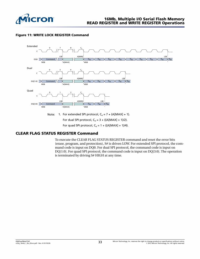
Figure 11: WRITE LOCK REGISTER Command
7 8 Cx0
C
MSB
DQ0
LSB
Command
A[MAX]
A[MIN]
MSB
DIN DIN DIN DIN DIN
LSBDIN DIN DIN DIN
3 4 Cx0
C
MSB
DQ[1:0]
LSB
Command
A[MAX]
A[MIN]
MSB
DIN DIN DIN DIN DIN
LSB
1 2 Cx0
C
MSB
DQ[3:0]
LSB
Command
A[MAX]
A[MIN]
MSB
DIN DIN DIN
LSB
Extended
Dual
Quad
Note: 1. For extended SPI protocol, Cx = 7 + (A[MAX] + 1).
For dual SPI protocol, Cx = 3 + ((A[MAX] + 1)/2).
For quad SPI protocol, Cx = 1 + ((A[MAX] + 1)/4).
CLEAR FLAG STATUS REGISTER Command
To execute the CLEAR FLAG STATUS REGISTER command and reset the error bits(erase, program, and protection), S# is driven LOW. For extended SPI protocol, the com-mand code is input on DQ0. For dual SPI protocol, the command code is input onDQ[1:0]. For quad SPI protocol, the command code is input on DQ[3:0]. The operationis terminated by driving S# HIGH at any time.
16Mb, Multiple I/O Serial Flash MemoryREAD REGISTER and WRITE REGISTER Operations
09005aef84a4754fn25q_16mb_1_8v_65nm.pdf - Rev. H 01/18 EN 33 Micron Technology, Inc. reserves the right to change products or specifications without notice.
© 2012 Micron Technology, Inc. All rights reserved.
READ IDENTIFICATION Operations
READ ID and MULTIPLE I/O READ ID Commands
To execute the READ ID or MULTIPLE I/O READ ID commands, S# is driven LOW andthe command code is input on DQn. The device outputs the information shown in thetables below. If an ERASE or PROGRAM cycle is in progress when the command is exe-cuted, the command is not decoded and the command cycle in progress is not affected.When S# is driven HIGH, the device goes to standby. The operation is terminated bydriving S# HIGH at any time during data output.
Table 18: Data/Address Lines for READ ID and MULTIPLE I/O READ ID Commands
Command Name Data In Data OutUnique IDis Output Extended Dual Quad
READ ID DQ0 DQ0 Yes Yes No No
MULTIPLE I/O READ ID DQ[3:0] DQ[1:0] No No Yes Yes
Note: 1. Yes in the protocol columns indicates that the command is supported and has the samefunctionality and command sequence as other commands marked Yes.
Table 19: Read ID Data Out
Size(Bytes) Name Content Value Assigned by
1 Manufacturer ID 20h JEDEC
2 Device ID
Memory Type BBh Manufacturer
Memory Capacity 15h (16Mb)
17 Unique ID
1 Byte: Length of data to follow 10h Factory
2 Bytes: Extended device ID and deviceconfiguration information
ID and information such as uniformarchitecture, and HOLDor RESET functionality
14 Bytes: Customized factory data Optional
Note: 1. The 17 bytes of information in the unique ID is read by the READ ID command, but can-not be read by the MULTIPLE I/O READ ID command.
Table 20: Extended Device ID, First Byte
Bit 7 Bit 6 Bit 5 Bit 4 Bit 3 Bit 2 Bit 1 Bit 0
Reserved Reserved 1 = Alternate BPscheme
0 = Standard BPscheme
Volatile configurationregister bit setting:
0 = Required1 = Not required
HOLD#/RESET#:0 = HOLD1 = RESET
Addressing:0 = by byte
Architecture:00 = Uniform
16Mb, Multiple I/O Serial Flash MemoryREAD IDENTIFICATION Operations
09005aef84a4754fn25q_16mb_1_8v_65nm.pdf - Rev. H 01/18 EN 34 Micron Technology, Inc. reserves the right to change products or specifications without notice.
© 2012 Micron Technology, Inc. All rights reserved.
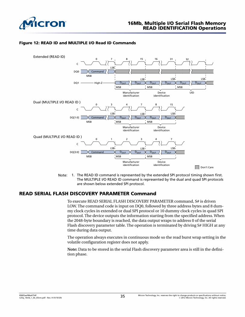
Figure 12: READ ID and MULTIPLE I/O Read ID Commands
UIDDeviceidentification
Manufactureridentification
High-ZDQ1
MSB MSB
DOUT DOUT DOUT DOUT
LSBLSB
7 8 15 16 32310
C
MSB
DQ0
LSB
Command
MSB
DOUT DOUT
LSB
Extended (READ ID)
Dual (MULTIPLE I/O READ ID )
Quad (MULTIPLE I/O READ ID )
Don’t Care
3 4 7 8 150
C
MSB
DQ[1:0]
LSB
Command
Deviceidentification
Manufactureridentification
MSB MSB
DOUT DOUT DOUT DOUT
LSBLSB
1 2 3 4 70
C
MSB
DQ[3:0]
LSB
Command
Deviceidentification
Manufactureridentification
MSB MSB
DOUT DOUT DOUT DOUT
LSBLSB
Note: 1. The READ ID command is represented by the extended SPI protocol timing shown first.The MULTIPLE I/O READ ID command is represented by the dual and quad SPI protocolsare shown below extended SPI protocol.
READ SERIAL FLASH DISCOVERY PARAMETER Command
To execute READ SERIAL FLASH DISCOVERY PARAMETER command, S# is drivenLOW. The command code is input on DQ0, followed by three address bytes and 8 dum-my clock cycles in extended or dual SPI protocol or 10 dummy clock cycles in quad SPIprotocol. The device outputs the information starting from the specified address. Whenthe 2048-byte boundary is reached, the data output wraps to address 0 of the serialFlash discovery parameter table. The operation is terminated by driving S# HIGH at anytime during data output.
The operation always executes in continuous mode so the read burst wrap setting in thevolatile configuration register does not apply.
Note: Data to be stored in the serial Flash discovery parameter area is still in the defini-tion phase.
16Mb, Multiple I/O Serial Flash MemoryREAD IDENTIFICATION Operations
09005aef84a4754fn25q_16mb_1_8v_65nm.pdf - Rev. H 01/18 EN 35 Micron Technology, Inc. reserves the right to change products or specifications without notice.
© 2012 Micron Technology, Inc. All rights reserved.
Table 21: Serial Flash Discovery Parameter Data Structure
Compliant with JEDEC standard JC-42.4 1775.03
DescriptionAddress
(Byte Mode) Address (Bit) Data
Serial Flash discoverable parameters signature 00h 7:0 53h
01h 7:0 46h
02h 7:0 44h
03h 7:0 50h
Serial Flash discoverable parameters Minor revision 04h 7:0 00h
Major revision 05h 7:0 01h
Number of parameter headers 06h 7:0 00h
Reserved 07h 7:0 FFh
Parameter ID (0) JEDEC-defined parameter table 08h 7:0 00h
Parameter Minor revision 09h 7:0 00h
Major revision 0Ah 7:0 01h
Parameter length (DW) 0Bh 7:0 09h
Parameter table pointer 0Ch 7:0 30h
0Dh 7:0 00h
0Eh 7:0 00h
Reserved 0Fh 7:0 FFh
Parameter ID (1) 10h 7:0 FFh
Parameter Minor revision 11h 7:0 FFh
Major revision 12h 7:0 FFh
Parameter length (DW) 13h 7:0 FFh
Parameter table pointer 14h 7:0 FFh
15h 7:0 FFh
16h 7:0 FFh
Reserved 17h 7:0 FFh
Parameter ID (2) 18h 7:0 FFh
Parameter Minor revision 19h 7:0 FFh
Major revision 1Ah 7:0 FFh
Parameter length (DW) 1Bh 7:0 FFh
Parameter table pointer 1Ch 7:0 FFh
1Dh 7:0 FFh
1Eh 7:0 FFh
Reserved 1Fh 7:0 FFh
16Mb, Multiple I/O Serial Flash MemoryREAD IDENTIFICATION Operations
09005aef84a4754fn25q_16mb_1_8v_65nm.pdf - Rev. H 01/18 EN 36 Micron Technology, Inc. reserves the right to change products or specifications without notice.
© 2012 Micron Technology, Inc. All rights reserved.
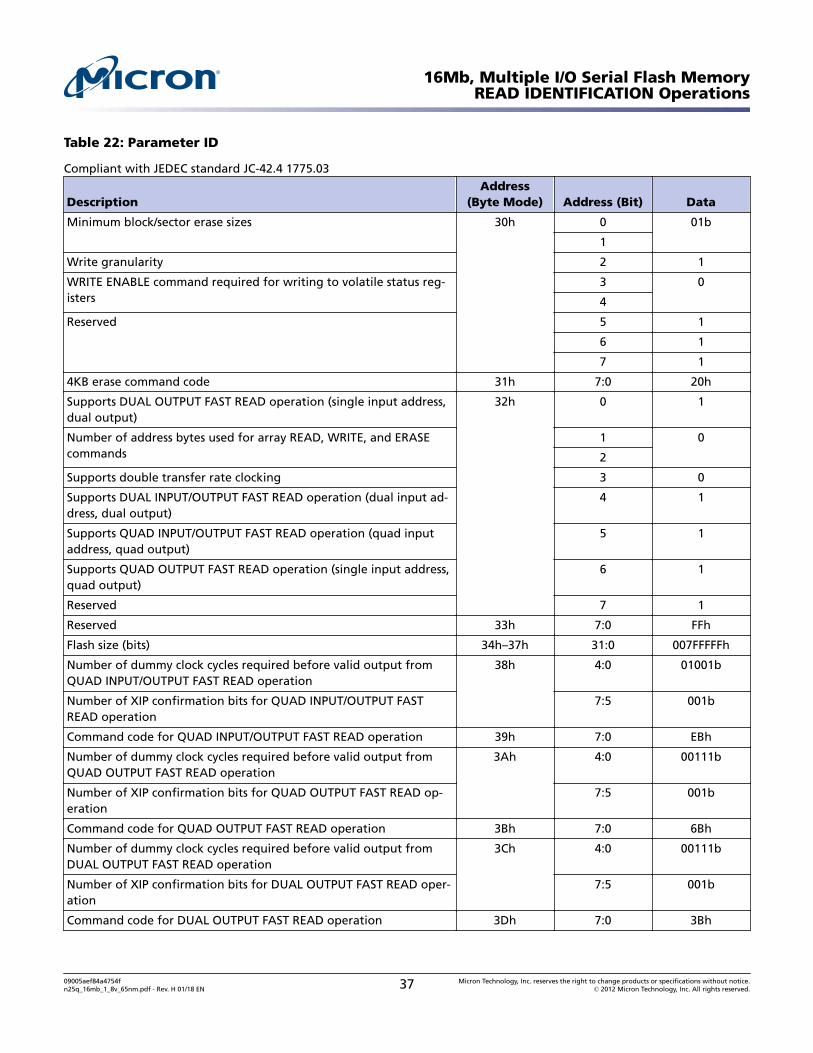
Table 22: Parameter ID
Compliant with JEDEC standard JC-42.4 1775.03
DescriptionAddress
(Byte Mode) Address (Bit) Data
Minimum block/sector erase sizes 30h 0 01b
1
Write granularity 2 1
WRITE ENABLE command required for writing to volatile status reg-isters
3 0
4
Reserved 5 1
6 1
7 1
4KB erase command code 31h 7:0 20h
Supports DUAL OUTPUT FAST READ operation (single input address,dual output)
32h 0 1
Number of address bytes used for array READ, WRITE, and ERASEcommands
1 0
2
Supports double transfer rate clocking 3 0
Supports DUAL INPUT/OUTPUT FAST READ operation (dual input ad-dress, dual output)
4 1
Supports QUAD INPUT/OUTPUT FAST READ operation (quad inputaddress, quad output)
5 1
Supports QUAD OUTPUT FAST READ operation (single input address,quad output)
6 1
Reserved 7 1
Reserved 33h 7:0 FFh
Flash size (bits) 34h–37h 31:0 007FFFFFh
Number of dummy clock cycles required before valid output fromQUAD INPUT/OUTPUT FAST READ operation
38h 4:0 01001b
Number of XIP confirmation bits for QUAD INPUT/OUTPUT FASTREAD operation
7:5 001b
Command code for QUAD INPUT/OUTPUT FAST READ operation 39h 7:0 EBh
Number of dummy clock cycles required before valid output fromQUAD OUTPUT FAST READ operation
3Ah 4:0 00111b
Number of XIP confirmation bits for QUAD OUTPUT FAST READ op-eration
7:5 001b
Command code for QUAD OUTPUT FAST READ operation 3Bh 7:0 6Bh
Number of dummy clock cycles required before valid output fromDUAL OUTPUT FAST READ operation
3Ch 4:0 00111b
Number of XIP confirmation bits for DUAL OUTPUT FAST READ oper-ation
7:5 001b
Command code for DUAL OUTPUT FAST READ operation 3Dh 7:0 3Bh
16Mb, Multiple I/O Serial Flash MemoryREAD IDENTIFICATION Operations
09005aef84a4754fn25q_16mb_1_8v_65nm.pdf - Rev. H 01/18 EN 37 Micron Technology, Inc. reserves the right to change products or specifications without notice.
© 2012 Micron Technology, Inc. All rights reserved.
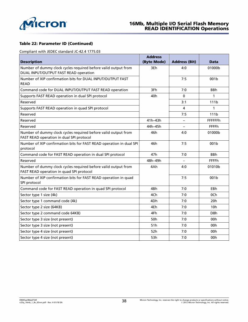
Table 22: Parameter ID (Continued)
Compliant with JEDEC standard JC-42.4 1775.03
DescriptionAddress
(Byte Mode) Address (Bit) Data
Number of dummy clock cycles required before valid output fromDUAL INPUT/OUTPUT FAST READ operation
3Eh 4:0 01000b
Number of XIP confirmation bits for DUAL INPUT/OUTPUT FASTREAD
7:5 001b
Command code for DUAL INPUT/OUTPUT FAST READ operation 3Fh 7:0 BBh
Supports FAST READ operation in dual SPI protocol 40h 0 1
Reserved 3:1 111b
Supports FAST READ operation in quad SPI protocol 4 1
Reserved 7:5 111b
Reserved 41h–43h – FFFFFFh
Reserved 44h–45h – FFFFh
Number of dummy clock cycles required before valid output fromFAST READ operation in dual SPI protocol
46h 4:0 01000b
Number of XIP confirmation bits for FAST READ operation in dual SPIprotocol
46h 7:5 001b
Command code for FAST READ operation in dual SPI protocol 47h 7:0 BBh
Reserved 48h–49h – FFFFh
Number of dummy clock cycles required before valid output fromFAST READ operation in quad SPI protocol
4Ah 4:0 01010b
Number of XIP confirmation bits for FAST READ operation in quadSPI protocol
7:5 001b
Command code for FAST READ operation in quad SPI protocol 4Bh 7:0 EBh
Sector type 1 size (4k) 4Ch 7:0 0Ch
Sector type 1 command code (4k) 4Dh 7:0 20h
Sector type 2 size (64KB) 4Eh 7:0 10h
Sector type 2 command code 64KB) 4Fh 7:0 D8h
Sector type 3 size (not present) 50h 7:0 00h
Sector type 3 size (not present) 51h 7:0 00h
Sector type 4 size (not present) 52h 7:0 00h
Sector type 4 size (not present) 53h 7:0 00h
16Mb, Multiple I/O Serial Flash MemoryREAD IDENTIFICATION Operations
09005aef84a4754fn25q_16mb_1_8v_65nm.pdf - Rev. H 01/18 EN 38 Micron Technology, Inc. reserves the right to change products or specifications without notice.
© 2012 Micron Technology, Inc. All rights reserved.
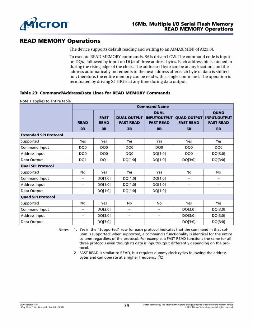
READ MEMORY OperationsThe device supports default reading and writing to an A[MAX:MIN] of A[23:0].
To execute READ MEMORY commands, S# is driven LOW. The command code is inputon DQn, followed by input on DQn of three address bytes. Each address bit is latched induring the rising edge of the clock. The addressed byte can be at any location, and theaddress automatically increments to the next address after each byte of data is shiftedout; therefore, the entire memory can be read with a single command. The operation isterminated by driving S# HIGH at any time during data output.
Table 23: Command/Address/Data Lines for READ MEMORY Commands
Note 1 applies to entire table
Command Name
READFASTREAD
DUAL OUTPUTFAST READ
DUALINPUT/OUTPUT
FAST READQUAD OUTPUT
FAST READ
QUADINPUT/OUTPUT
FAST READ
03 0B 3B BB 6B EB
Extended SPI Protocol
Supported Yes Yes Yes Yes Yes Yes
Command Input DQ0 DQ0 DQ0 DQ0 DQ0 DQ0
Address Input DQ0 DQ0 DQ0 DQ[1:0] DQ0 DQ[3:0]
Data Output DQ1 DQ1 DQ[1:0] DQ[1:0] DQ[3:0] DQ[3:0]
Dual SPI Protocol
Supported No Yes Yes Yes No No
Command Input – DQ[1:0] DQ[1:0] DQ[1:0] – –
Address Input – DQ[1:0] DQ[1:0] DQ[1:0] – –
Data Output – DQ[1:0] DQ[1:0] DQ[1:0] – –
Quad SPI Protocol
Supported No Yes No No Yes Yes
Command Input – DQ[3:0] – – DQ[3:0] DQ[3:0]
Address Input – DQ[3:0] – – DQ[3:0] DQ[3:0]
Data Output – DQ[3:0] – – DQ[3:0] DQ[3:0]
Notes: 1. Yes in the "Supported" row for each protocol indicates that the command in that col-umn is supported; when supported, a command's functionality is identical for the entirecolumn regardless of the protocol. For example, a FAST READ functions the same for allthree protocols even though its data is input/output differently depending on the pro-tocol.
2. FAST READ is similar to READ, but requires dummy clock cycles following the addressbytes and can operate at a higher frequency (fC).
16Mb, Multiple I/O Serial Flash MemoryREAD MEMORY Operations
09005aef84a4754fn25q_16mb_1_8v_65nm.pdf - Rev. H 01/18 EN 39 Micron Technology, Inc. reserves the right to change products or specifications without notice.
© 2012 Micron Technology, Inc. All rights reserved.
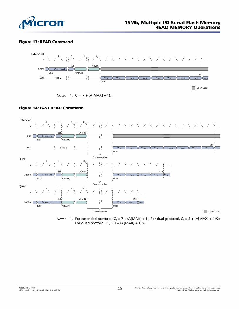
Figure 13: READ Command
Don’t Care
MSB
DQ[0]
LSB
Command
A[MAX]
A[MIN]
7 8 Cx0
C
Extended
High-ZDQ1
MSB
DOUT DOUT DOUT DOUT DOUT
LSBDOUT DOUT DOUT DOUT
Note: 1. Cx = 7 + (A[MAX] + 1).
Figure 14: FAST READ Command
7 8 Cx0
C
MSB
DQ0
LSB
Command
A[MAX]
A[MIN]
3 4 Cx0
C
MSB
DQ[1:0]
LSB
Command
A[MAX]
A[MIN]
MSB
DOUT DOUT DOUT DOUT DOUT
LSB
Dummy cycles
1 2 Cx0
C
MSB
DQ[3:0]
LSB
Command
A[MAX]
A[MIN]
MSB
DOUT DOUT DOUT
LSB
Dummy cycles
Extended
MSB
DOUT DOUT DOUT DOUT DOUT
LSBDOUT DOUT DOUT DOUT
Dummy cyclesDual
Quad
DQ1 High-Z
Don’t Care
Note: 1. For extended protocol, Cx = 7 + (A[MAX] + 1); For dual protocol, Cx = 3 + (A[MAX] + 1)/2;For quad protocol, Cx = 1 + (A[MAX] + 1)/4.
16Mb, Multiple I/O Serial Flash MemoryREAD MEMORY Operations
09005aef84a4754fn25q_16mb_1_8v_65nm.pdf - Rev. H 01/18 EN 40 Micron Technology, Inc. reserves the right to change products or specifications without notice.
© 2012 Micron Technology, Inc. All rights reserved.
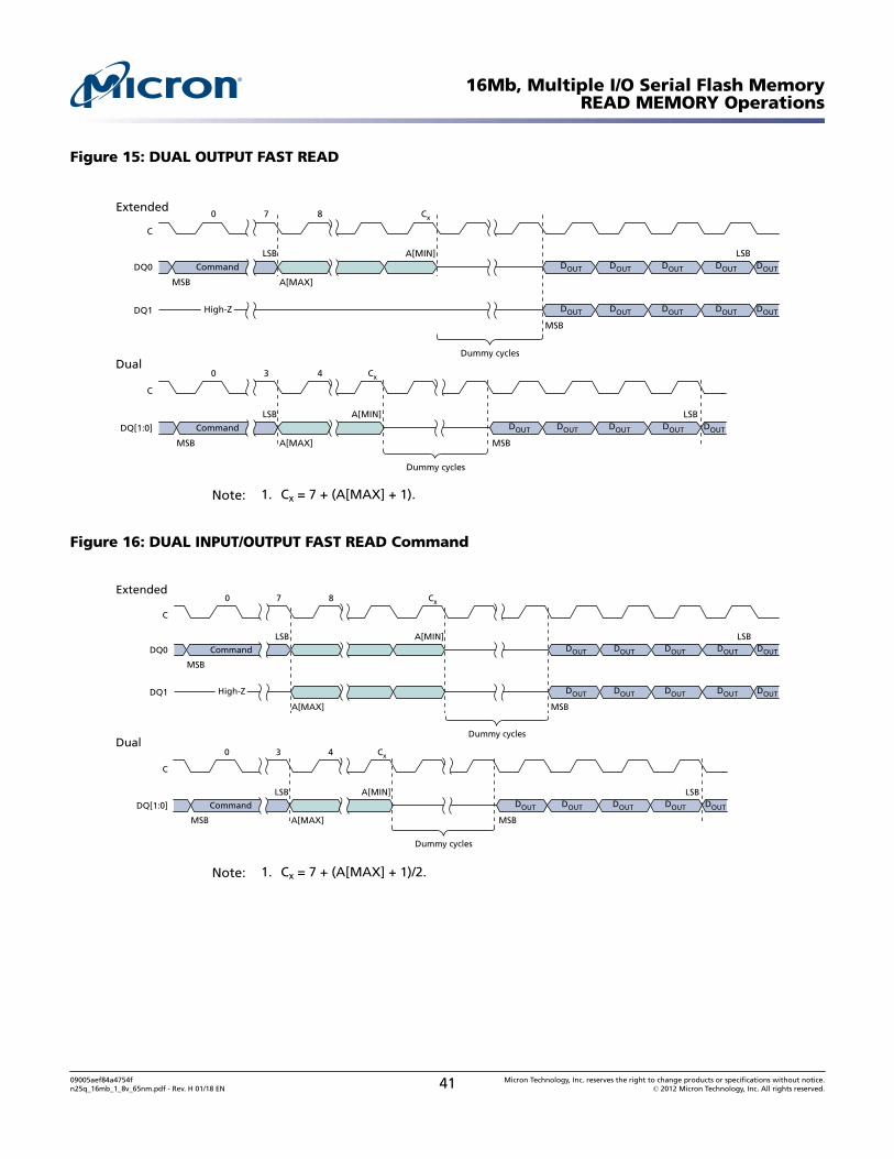
Figure 15: DUAL OUTPUT FAST READ
7 8 Cx0
C
MSB
DQ0
LSB
Command DOUT
LSB
DQ1 DOUT
A[MAX]
High-Z
A[MIN]DOUT
MSB
DOUT
DOUT
DOUT
DOUT
DOUT
DOUT
DOUT
Dummy cycles
DQ[1:0]
Dual
Extended
3 4 Cx0
C
MSB
LSB
Command
A[MAX]
A[MIN]
MSB
DOUT DOUT DOUT DOUT DOUT
LSB
Dummy cycles
Note: 1. Cx = 7 + (A[MAX] + 1).
Figure 16: DUAL INPUT/OUTPUT FAST READ Command
7 8 Cx0
C
MSB
DQ0
LSB
Command DOUT
LSB
DQ1 DOUTHigh-Z
A[MIN]DOUT
MSB
DOUT
DOUT
DOUT
DOUT
DOUT
DOUT
DOUT
A[MAX]
Dummy cycles
3 4 Cx0
C
MSB
DQ[1:0]
LSB
Command
A[MAX]
A[MIN]
MSB
DOUT DOUT DOUT DOUT DOUT
LSB
Dummy cycles
Dual
Extended
Note: 1. Cx = 7 + (A[MAX] + 1)/2.
16Mb, Multiple I/O Serial Flash MemoryREAD MEMORY Operations
09005aef84a4754fn25q_16mb_1_8v_65nm.pdf - Rev. H 01/18 EN 41 Micron Technology, Inc. reserves the right to change products or specifications without notice.
© 2012 Micron Technology, Inc. All rights reserved.
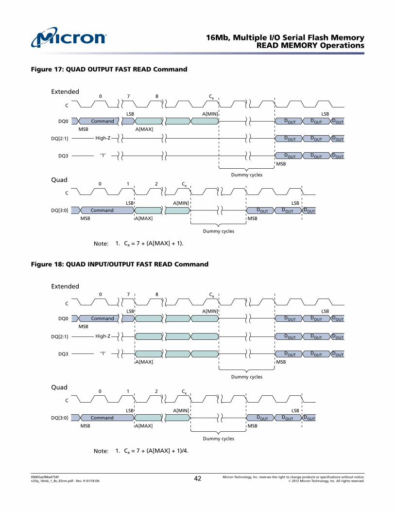
Figure 17: QUAD OUTPUT FAST READ Command
Dummy cycles
7 8 Cx0
C
MSB
DQ0
LSB
Command DOUT
LSB
DQ[2:1] DOUT
A[MAX]
High-Z
A[MIN]DOUT
DOUT
DOUT
DOUT
DQ3 DOUT‘1’
MSB
DOUT DOUT
1 2 Cx0
C
MSB
DQ[3:0]
LSB
Command
A[MAX]
A[MIN]
MSB
DOUT DOUT DOUT
LSB
Dummy cycles
Quad
Extended
Note: 1. Cx = 7 + (A[MAX] + 1).
Figure 18: QUAD INPUT/OUTPUT FAST READ Command
Dummy cycles
7 8 Cx0
C
MSB
DQ0
LSB
Command DOUT
LSB
DQ[2:1] DOUTHigh-Z
A[MIN]DOUT
DOUT
DOUT
DOUT
DQ3 DOUT‘1’
MSB
DOUT DOUT
A[MAX]
1 2 Cx0
C
MSB
DQ[3:0]
LSB
Command
A[MAX]
A[MIN]
MSB
DOUT DOUT DOUT
LSB
Dummy cycles
Quad
Extended
Note: 1. Cx = 7 + (A[MAX] + 1)/4.
16Mb, Multiple I/O Serial Flash MemoryREAD MEMORY Operations
09005aef84a4754fn25q_16mb_1_8v_65nm.pdf - Rev. H 01/18 EN 42 Micron Technology, Inc. reserves the right to change products or specifications without notice.
© 2012 Micron Technology, Inc. All rights reserved.
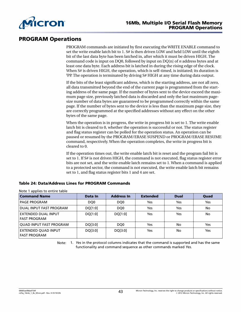
PROGRAM OperationsPROGRAM commands are initiated by first executing the WRITE ENABLE command toset the write enable latch bit to 1. S# is then driven LOW and held LOW until the eighthbit of the last data byte has been latched in, after which it must be driven HIGH. Thecommand code is input on DQ0, followed by input on DQ[n] of n address bytes and atleast one data byte. Each address bit is latched in during the rising edge of the clock.When S# is driven HIGH, the operation, which is self-timed, is initiated; its duration istPP. The operation is terminated by driving S# HIGH at any time during data output.
If the bits of the least significant address, which is the starting address, are not all zero,all data transmitted beyond the end of the current page is programmed from the start-ing address of the same page. If the number of bytes sent to the device exceed the maxi-mum page size, previously latched data is discarded and only the last maximum page-size number of data bytes are guaranteed to be programmed correctly within the samepage. If the number of bytes sent to the device is less than the maximum page size, theyare correctly programmed at the specified addresses without any effect on the otherbytes of the same page.
When the operation is in progress, the write in progress bit is set to 1. The write enablelatch bit is cleared to 0, whether the operation is successful or not. The status registerand flag status register can be polled for the operation status. An operation can bepaused or resumed by the PROGRAM/ERASE SUSPEND or PROGRAM/ERASE RESUMEcommand, respectively. When the operation completes, the write in progress bit iscleared to 0.
If the operation times out, the write enable latch bit is reset and the program fail bit isset to 1. If S# is not driven HIGH, the command is not executed, flag status register errorbits are not set, and the write enable latch remains set to 1. When a command is appliedto a protected sector, the command is not executed, the write enable latch bit remainsset to 1, and flag status register bits 1 and 4 are set.
Table 24: Data/Address Lines for PROGRAM Commands
Note 1 applies to entire tableCommand Name Data In Address In Extended Dual Quad
PAGE PROGRAM DQ0 DQ0 Yes Yes Yes
DUAL INPUT FAST PROGRAM DQ[1:0] DQ0 Yes Yes No
EXTENDED DUAL INPUTFAST PROGRAM
DQ[1:0] DQ[1:0] Yes Yes No
QUAD INPUT FAST PROGRAM DQ[3:0] DQ0 Yes No Yes
EXTENDED QUAD INPUTFAST PROGRAM
DQ[3:0] DQ[3:0] Yes No Yes
Note: 1. Yes in the protocol columns indicates that the command is supported and has the samefunctionality and command sequence as other commands marked Yes.
16Mb, Multiple I/O Serial Flash MemoryPROGRAM Operations
09005aef84a4754fn25q_16mb_1_8v_65nm.pdf - Rev. H 01/18 EN 43 Micron Technology, Inc. reserves the right to change products or specifications without notice.
© 2012 Micron Technology, Inc. All rights reserved.
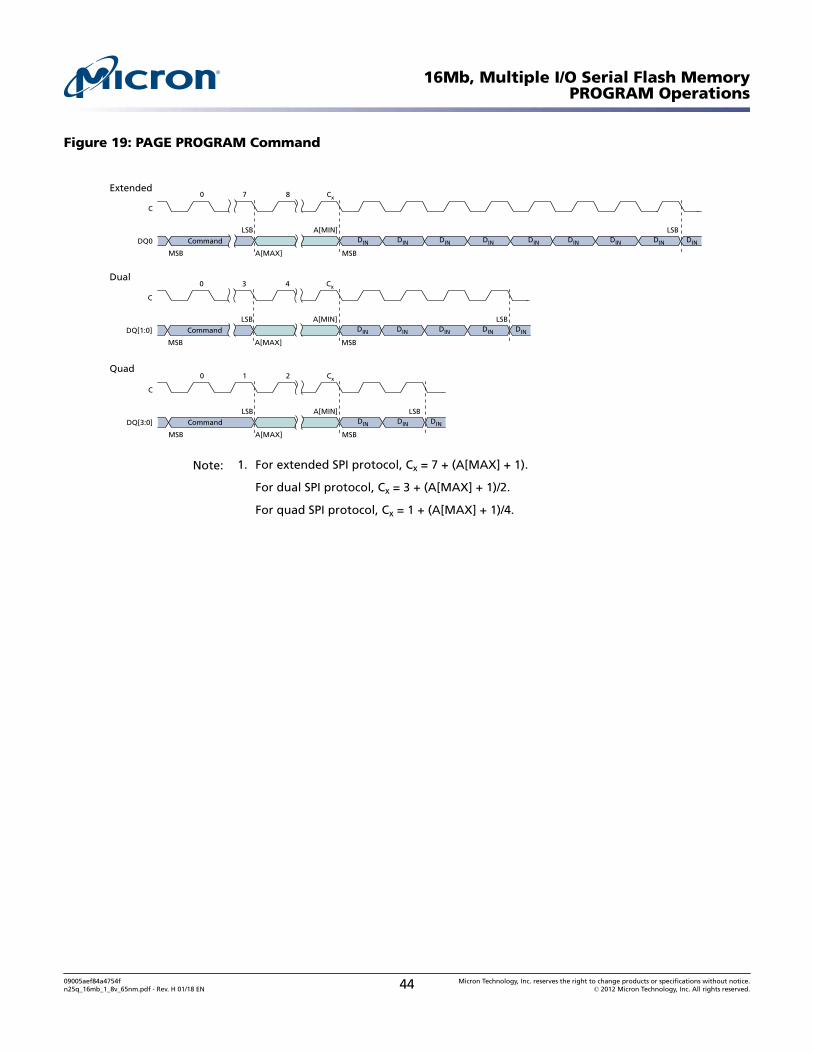
Figure 19: PAGE PROGRAM Command
7 8 Cx0
C
MSB
DQ0
LSB
Command
A[MAX]
A[MIN]
MSB
DIN DIN DIN DIN DIN
LSBDIN DIN DIN DIN
3 4 Cx0
C
MSB
DQ[1:0]
LSB
Command
A[MAX]
A[MIN]
MSB
DIN DIN DIN DIN DIN
LSB
1 2 Cx0
C
MSB
DQ[3:0]
LSB
Command
A[MAX]
A[MIN]
MSB
DIN DIN DIN
LSB
Extended
Dual
Quad
Note: 1. For extended SPI protocol, Cx = 7 + (A[MAX] + 1).
For dual SPI protocol, Cx = 3 + (A[MAX] + 1)/2.
For quad SPI protocol, Cx = 1 + (A[MAX] + 1)/4.
16Mb, Multiple I/O Serial Flash MemoryPROGRAM Operations
09005aef84a4754fn25q_16mb_1_8v_65nm.pdf - Rev. H 01/18 EN 44 Micron Technology, Inc. reserves the right to change products or specifications without notice.
© 2012 Micron Technology, Inc. All rights reserved.
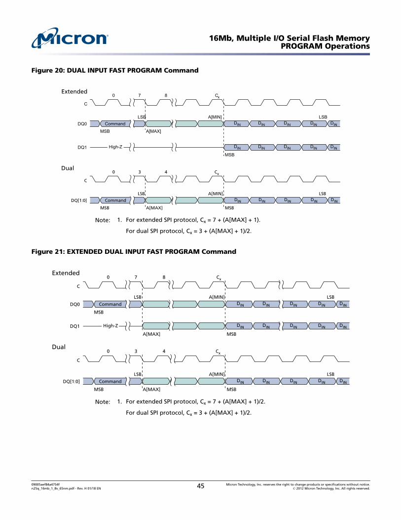
Figure 20: DUAL INPUT FAST PROGRAM Command
Extended
Dual3 4 Cx0
C
MSB
DQ[1:0]
LSB
Command DIN
LSB
A[MAX]
A[MIN]
MSB
DIN DIN DIN DIN
7 8 Cx0
C
MSBDQ0
LSBCommand DIN
LSB
DQ1 DIN
A[MAX]
High-Z
A[MIN]DIN
MSB
DIN
DIN
DIN
DIN
DIN
DIN
DIN
Note: 1. For extended SPI protocol, Cx = 7 + (A[MAX] + 1).
For dual SPI protocol, Cx = 3 + (A[MAX] + 1)/2.
Figure 21: EXTENDED DUAL INPUT FAST PROGRAM Command
Extended
Dual3 4 Cx0
C
MSB
DQ[1:0]
LSB
Command DIN
LSB
A[MAX]
A[MIN]
MSB
DIN DIN DIN DIN
7 8 Cx0
C
MSB
DQ0
LSB
Command DIN
LSB
DQ1 DINHigh-Z
A[MIN]
A[MAX]
DIN
MSB
DIN
DIN
DIN
DIN
DIN
DIN
DIN
Note: 1. For extended SPI protocol, Cx = 7 + (A[MAX] + 1)/2.
For dual SPI protocol, Cx = 3 + (A[MAX] + 1)/2.
16Mb, Multiple I/O Serial Flash MemoryPROGRAM Operations
09005aef84a4754fn25q_16mb_1_8v_65nm.pdf - Rev. H 01/18 EN 45 Micron Technology, Inc. reserves the right to change products or specifications without notice.
© 2012 Micron Technology, Inc. All rights reserved.
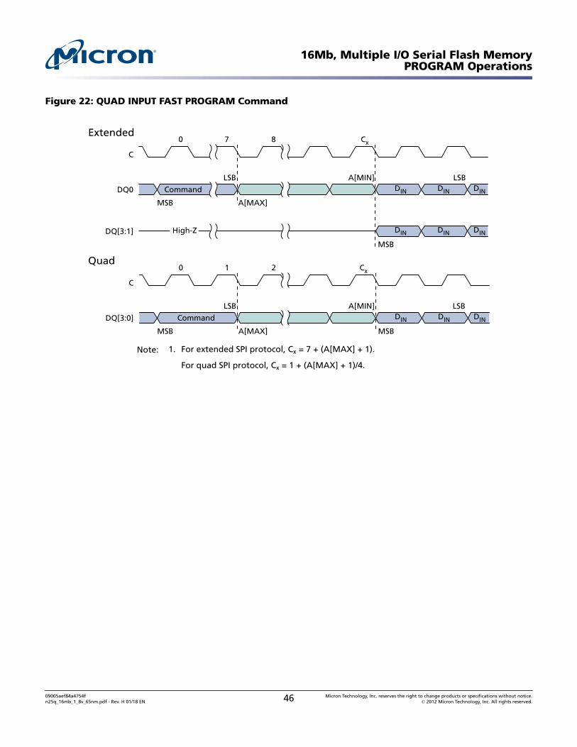
Figure 22: QUAD INPUT FAST PROGRAM Command
7 8 Cx0
C
MSB
DQ0
LSB
Command DIN
LSB
DQ[3:1] DIN
A[MAX]
High-Z
A[MIN]DIN
MSB
DIN
DIN
DIN
Extended
Quad1 2 Cx0
C
MSB
DQ[3:0]
LSB
Command DIN
LSB
A[MAX]
A[MIN]
MSB
DIN DIN
Note: 1. For extended SPI protocol, Cx = 7 + (A[MAX] + 1).
For quad SPI protocol, Cx = 1 + (A[MAX] + 1)/4.
16Mb, Multiple I/O Serial Flash MemoryPROGRAM Operations
09005aef84a4754fn25q_16mb_1_8v_65nm.pdf - Rev. H 01/18 EN 46 Micron Technology, Inc. reserves the right to change products or specifications without notice.
© 2012 Micron Technology, Inc. All rights reserved.
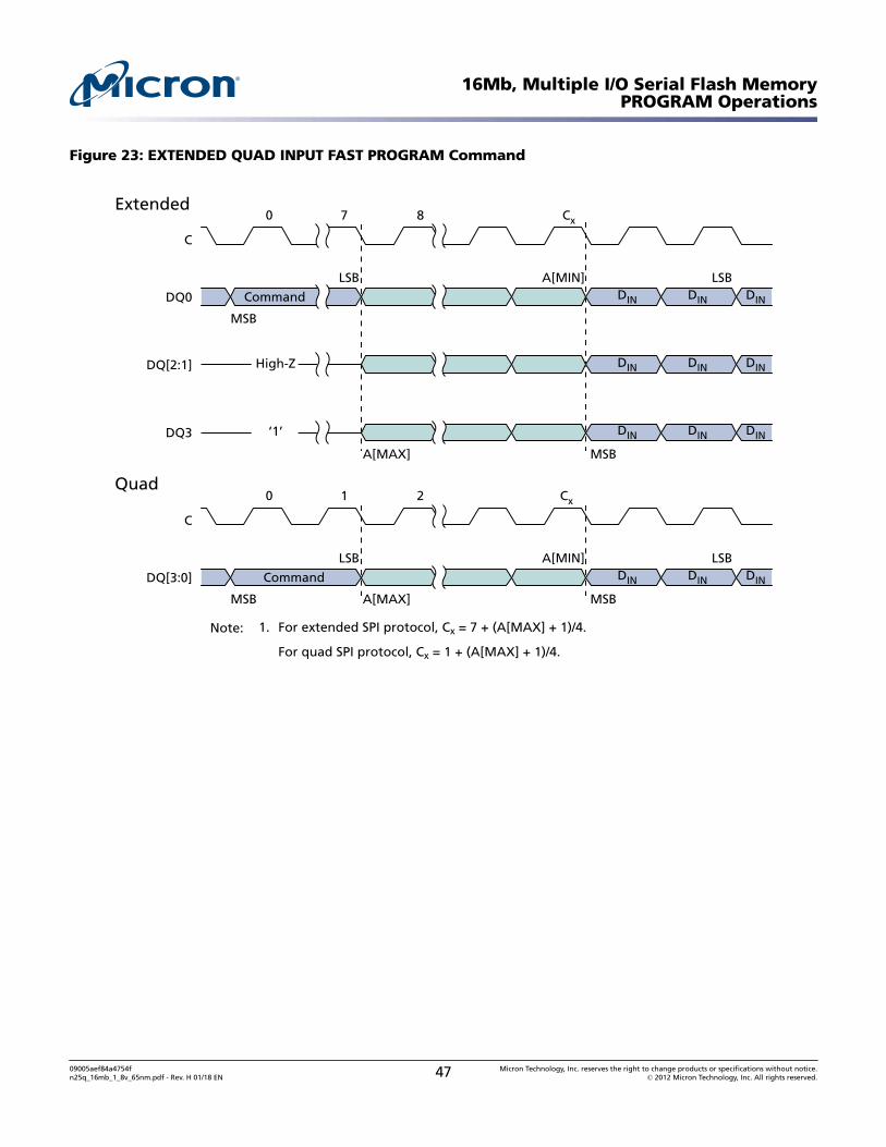
Figure 23: EXTENDED QUAD INPUT FAST PROGRAM Command
7 8 Cx0
C
MSB
DQ0
LSB
Command DIN
LSB
DQ[2:1] DINHigh-Z
A[MIN]
A[MAX]
DIN
DIN
DIN
DIN
DQ3 DIN‘1’
MSB
DIN DIN
Extended
Quad1 2 Cx0
C
MSB
DQ[3:0]
LSB
Command DIN
LSB
A[MAX]
A[MIN]
MSB
DIN DIN
Note: 1. For extended SPI protocol, Cx = 7 + (A[MAX] + 1)/4.
For quad SPI protocol, Cx = 1 + (A[MAX] + 1)/4.
16Mb, Multiple I/O Serial Flash MemoryPROGRAM Operations
09005aef84a4754fn25q_16mb_1_8v_65nm.pdf - Rev. H 01/18 EN 47 Micron Technology, Inc. reserves the right to change products or specifications without notice.
© 2012 Micron Technology, Inc. All rights reserved.
WRITE Operations
WRITE ENABLE Command
The WRITE ENABLE operation sets the write enable latch bit. To execute a WRITE ENA-BLE command, S# is driven LOW and held LOW until the eighth bit of the commandcode has been latched in, after which it must be driven HIGH. The command code isinput on DQ0 for extended SPI protocol, on DQ[1:0] for dual SPI protocol, and onDQ[3:0] for quad SPI protocol.
The write enable latch bit must be set before every PROGRAM, ERASE, and WRITE com-mand. If S# is not driven HIGH after the command code has been latched in, the com-mand is not executed, flag status register error bits are not set, and the write enablelatch remains cleared to its default setting of 0.
WRITE DISABLE Command
The WRITE DISABLE operation clears the write enable latch bit. To execute a WRITEDISABLE command, S# is driven LOW and held LOW until the eighth bit of the com-mand code has been latched in, after which it must be driven HIGH. The commandcode is input on DQ0 for extended SPI protocol, on DQ[1:0] for dual SPI protocol, andon DQ[3:0] for quad SPI protocol.
If S# is not driven HIGH after the command code has been latched in, the command isnot executed, flag status register error bits are not set, and the write enable latch re-mains set to 1.
16Mb, Multiple I/O Serial Flash MemoryWRITE Operations
09005aef84a4754fn25q_16mb_1_8v_65nm.pdf - Rev. H 01/18 EN 48 Micron Technology, Inc. reserves the right to change products or specifications without notice.
© 2012 Micron Technology, Inc. All rights reserved.
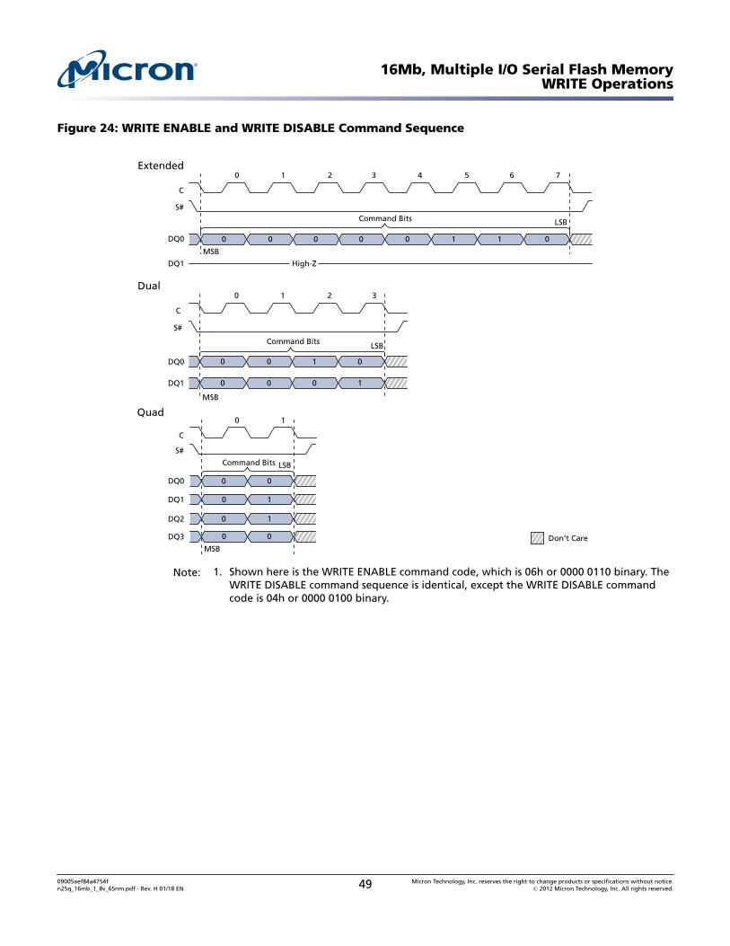
Figure 24: WRITE ENABLE and WRITE DISABLE Command Sequence
DQ0
MSB
LSB
Dual
Don’t Care
Command Bits
DQ0
0 1 2 4 53 76
C
Extended
High-ZDQ1
MSB
LSB
0 0 0 0 0 011
Command BitsS#
S#
0 0 1 0
MSB
10
C
LSB
DQ1
DQ2
Quad
Command Bits
S#
0
0
DQ3 0 0
DQ0 0 0
1
1
DQ1 0 0 0 1
1 20
C
3
Note: 1. Shown here is the WRITE ENABLE command code, which is 06h or 0000 0110 binary. TheWRITE DISABLE command sequence is identical, except the WRITE DISABLE commandcode is 04h or 0000 0100 binary.
16Mb, Multiple I/O Serial Flash MemoryWRITE Operations
09005aef84a4754fn25q_16mb_1_8v_65nm.pdf - Rev. H 01/18 EN 49 Micron Technology, Inc. reserves the right to change products or specifications without notice.
© 2012 Micron Technology, Inc. All rights reserved.
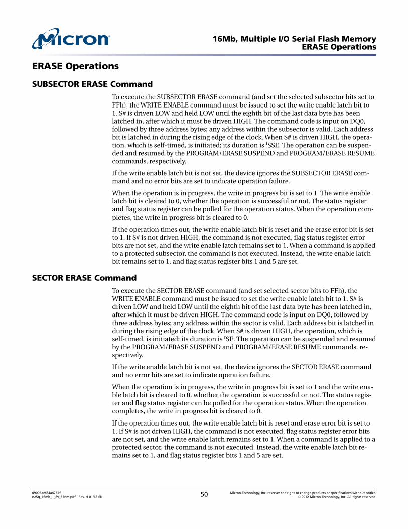
ERASE Operations
SUBSECTOR ERASE Command
To execute the SUBSECTOR ERASE command (and set the selected subsector bits set toFFh), the WRITE ENABLE command must be issued to set the write enable latch bit to1. S# is driven LOW and held LOW until the eighth bit of the last data byte has beenlatched in, after which it must be driven HIGH. The command code is input on DQ0,followed by three address bytes; any address within the subsector is valid. Each addressbit is latched in during the rising edge of the clock. When S# is driven HIGH, the opera-tion, which is self-timed, is initiated; its duration is tSSE. The operation can be suspen-ded and resumed by the PROGRAM/ERASE SUSPEND and PROGRAM/ERASE RESUMEcommands, respectively.
If the write enable latch bit is not set, the device ignores the SUBSECTOR ERASE com-mand and no error bits are set to indicate operation failure.
When the operation is in progress, the write in progress bit is set to 1. The write enablelatch bit is cleared to 0, whether the operation is successful or not. The status registerand flag status register can be polled for the operation status. When the operation com-pletes, the write in progress bit is cleared to 0.
If the operation times out, the write enable latch bit is reset and the erase error bit is setto 1. If S# is not driven HIGH, the command is not executed, flag status register errorbits are not set, and the write enable latch remains set to 1. When a command is appliedto a protected subsector, the command is not executed. Instead, the write enable latchbit remains set to 1, and flag status register bits 1 and 5 are set.
SECTOR ERASE Command
To execute the SECTOR ERASE command (and set selected sector bits to FFh), theWRITE ENABLE command must be issued to set the write enable latch bit to 1. S# isdriven LOW and held LOW until the eighth bit of the last data byte has been latched in,after which it must be driven HIGH. The command code is input on DQ0, followed bythree address bytes; any address within the sector is valid. Each address bit is latched induring the rising edge of the clock. When S# is driven HIGH, the operation, which isself-timed, is initiated; its duration is tSE. The operation can be suspended and resumedby the PROGRAM/ERASE SUSPEND and PROGRAM/ERASE RESUME commands, re-spectively.
If the write enable latch bit is not set, the device ignores the SECTOR ERASE commandand no error bits are set to indicate operation failure.
When the operation is in progress, the write in progress bit is set to 1 and the write ena-ble latch bit is cleared to 0, whether the operation is successful or not. The status regis-ter and flag status register can be polled for the operation status. When the operationcompletes, the write in progress bit is cleared to 0.
If the operation times out, the write enable latch bit is reset and erase error bit is set to1. If S# is not driven HIGH, the command is not executed, flag status register error bitsare not set, and the write enable latch remains set to 1. When a command is applied to aprotected sector, the command is not executed. Instead, the write enable latch bit re-mains set to 1, and flag status register bits 1 and 5 are set.
16Mb, Multiple I/O Serial Flash MemoryERASE Operations
09005aef84a4754fn25q_16mb_1_8v_65nm.pdf - Rev. H 01/18 EN 50 Micron Technology, Inc. reserves the right to change products or specifications without notice.
© 2012 Micron Technology, Inc. All rights reserved.
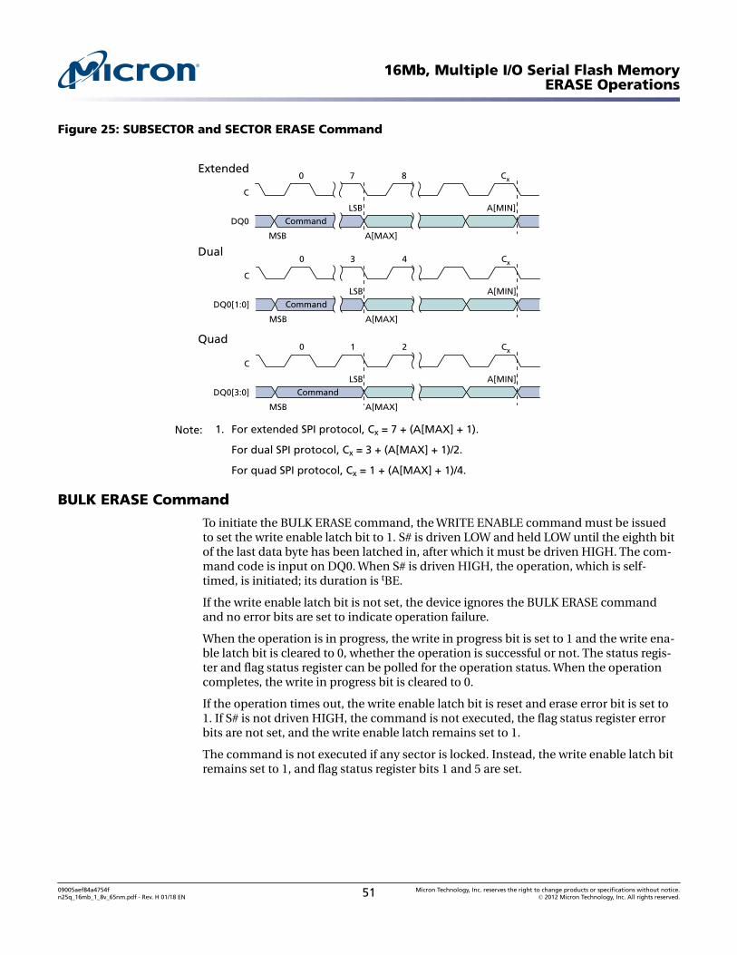
Figure 25: SUBSECTOR and SECTOR ERASE Command
7 8 Cx0
C
MSB
DQ0
LSB
Command
A[MAX]
A[MIN]
3 4 Cx0
C
MSB
DQ0[1:0]
LSB
Command
A[MAX]
A[MIN]
1 2 Cx0
C
MSB
DQ0[3:0]
LSB
Command
A[MAX]
A[MIN]
Extended
Dual
Quad
Note: 1. For extended SPI protocol, Cx = 7 + (A[MAX] + 1).
For dual SPI protocol, Cx = 3 + (A[MAX] + 1)/2.
For quad SPI protocol, Cx = 1 + (A[MAX] + 1)/4.
BULK ERASE Command
To initiate the BULK ERASE command, the WRITE ENABLE command must be issuedto set the write enable latch bit to 1. S# is driven LOW and held LOW until the eighth bitof the last data byte has been latched in, after which it must be driven HIGH. The com-mand code is input on DQ0. When S# is driven HIGH, the operation, which is self-timed, is initiated; its duration is tBE.
If the write enable latch bit is not set, the device ignores the BULK ERASE commandand no error bits are set to indicate operation failure.
When the operation is in progress, the write in progress bit is set to 1 and the write ena-ble latch bit is cleared to 0, whether the operation is successful or not. The status regis-ter and flag status register can be polled for the operation status. When the operationcompletes, the write in progress bit is cleared to 0.
If the operation times out, the write enable latch bit is reset and erase error bit is set to1. If S# is not driven HIGH, the command is not executed, the flag status register errorbits are not set, and the write enable latch remains set to 1.
The command is not executed if any sector is locked. Instead, the write enable latch bitremains set to 1, and flag status register bits 1 and 5 are set.
16Mb, Multiple I/O Serial Flash MemoryERASE Operations
09005aef84a4754fn25q_16mb_1_8v_65nm.pdf - Rev. H 01/18 EN 51 Micron Technology, Inc. reserves the right to change products or specifications without notice.
© 2012 Micron Technology, Inc. All rights reserved.
Figure 26: BULK ERASE Command
70
C
MSB
DQ0
LSB
Command
30
C
MSB
DQ[1:0]
LSB
Command
10
C
MSB
DQ[3:0]
LSB
Command
Extended
Dual
Quad
PROGRAM/ERASE SUSPEND Command
To initiate the PROGRAM/ERASE SUSPEND command, S# is driven LOW. The com-mand code is input on DQ0. The operation is terminated by the PROGRAM/ERASE RE-SUME command.
PROGRAM/ERASE SUSPEND command enables the memory controller to interruptand suspend an array PROGRAM or ERASE operation within the program/erase latency.
If a SUSPEND command is issued during a PROGRAM operation, then the flag statusregister bit 2 is set to 1. After erase/program latency time, the flag status register bit 7 isalso set to 1, showing the device to be in a suspended state, waiting for any operation(see the Operations Allowed/Disallowed During Device States table).
If a SUSPEND command is issued during an ERASE operation, then the flag status regis-ter bit 6 is set to 1. After erase/program latency time, the flag status register bit 7 is alsoset to 1, showing that device to be in a suspended state, waiting for any operation (seethe Operations Allowed/Disallowed During Device States table).
If the time remaining to complete the operation is less than the suspend latency, the de-vice completes the operation and clears the flag status register bits 2 or 6, as applicable.Because the suspend state is volatile, if there is a power cycle, the suspend state infor-mation is lost and the flag status register powers up as 80h.
During an ERASE SUSPEND operation, a PROGRAM or READ operation is possible inany sector except the one in a suspended state. Reading from a sector that is in a sus-pended state will output indeterminate data. The device ignores a PROGRAM com-mand to a sector that is in an ERASE SUSPEND state; it also sets the flag status registerbit 4 to 1: program failure/protection error, and leaves the write enable latch bit un-changed. The commands allowed during an erase suspend state include the WRITELOCK REGISTER command, the WRITE VOLATILE CONFIGURATION REGISTER com-
16Mb, Multiple I/O Serial Flash MemoryERASE Operations
09005aef84a4754fn25q_16mb_1_8v_65nm.pdf - Rev. H 01/18 EN 52 Micron Technology, Inc. reserves the right to change products or specifications without notice.
© 2012 Micron Technology, Inc. All rights reserved.
mand, and the WRITE ENHANCED VOLATILE CONFIGURATION REGISTER command.When the ERASE operation resumes, it does not check the new lock status of the WRITELOCK REGISTER command.
During a PROGRAM SUSPEND operation, a READ operation is possible in any page ex-cept the one in a suspended state. Reading from a page that is in a suspended state willoutput indeterminate data. The commands allowed during a program suspend state in-clude the WRITE VOLATILE CONFIGURATION REGISTER command and the WRITEENHANCED VOLATILE CONFIGURATION REGISTER command.
It is possible to nest a PROGRAM/ERASE SUSPEND operation inside a PROGRAM/ERASE SUSPEND operation just once. Issue an ERASE command and suspend it. Thenissue a PROGRAM command and suspend it also. With the two operations suspended,the next PROGRAM/ERASE RESUME command resumes the latter operation, and a sec-ond PROGRAM/ERASE RESUME command resumes the former (or first) operation.
Table 25: Suspend Parameters
Parameter Condition Typ Max Units Notes
Erase to suspend Sector erase or erase resume to erase suspend 150 – µs 1
Program to suspend Program resume to program suspend 5 – µs 1
Subsector erase to sus-pend
Subsector erase or subsector erase resume to erase sus-pend
50 – µs 1
Suspend latency Program 7 – µs 2
Suspend latency Subsector erase 15 – µs 2
Suspend latency Erase 15 – µs 3
Notes: 1. Timing is not internally controlled.2. Any READ command accepted.3. Any command except the following are accepted: SECTOR, SUBSECTOR, or BULK ERASE;
WRITE STATUS REGISTER; WRITE NONVOLATILE CONFIGURATION REGISTER; and PRO-GRAM OTP.
Table 26: Operations Allowed/Disallowed During Device States
Note 1 applies to entire table
OperationStandby
StateProgram orErase State
Subsector Erase Suspend orProgram Suspend State
Erase SuspendState Notes
READ Yes No Yes Yes 2
PROGRAM Yes No No Yes/No 3
ERASE Yes No No No 4
WRITE Yes No No No 5
WRITE Yes No Yes Yes 6
READ Yes Yes Yes Yes 7
SUSPEND No Yes No No 8
Notes: 1. The device can be in only one state at a time. Depending on the state of the device,some operations are allowed (Yes) and others are not (No). For example, when the de-vice is in the standby state, all operations except SUSPEND are allowed in any sector. Forall device states except the erase suspend state, if an operation is allowed or disallowed
16Mb, Multiple I/O Serial Flash MemoryERASE Operations
09005aef84a4754fn25q_16mb_1_8v_65nm.pdf - Rev. H 01/18 EN 53 Micron Technology, Inc. reserves the right to change products or specifications without notice.
© 2012 Micron Technology, Inc. All rights reserved.
in one sector, it is allowed or disallowed in all other sectors. In the erase suspend state, aPROGRAM operation is allowed in any sector except the one in which an ERASE opera-tion has been suspended.
2. All READ operations except READ STATUS REGISTER and READ FLAG REGISTER. When is-sued to a sector or subsector that is simultaneously in an erase suspend state, the READoperation is accepted, but the data output is not guaranteed until the erase has comple-ted.
3. All PROGRAM operations except PROGRAM OTP. In the erase suspend state, a PROGRAMoperation is allowed in any sector (Yes) except the sector (No) in which an ERASE opera-tion has been suspended.
4. Applies to the SECTOR ERASE or SUBSECTOR ERASE operation.5. Applies to the following operations: WRITE STATUS REGISTER, WRITE NONVOLATILE
CONFIGURATION REGISTER, PROGRAM OTP, and BULK ERASE.6. Applies to the following operations: WRITE ENABLE, WRITE DISABLE, CLEAR FLAG STA-
TUS REGISTER, WRITE LOCK REGISTER, WRITE VOLATILE, and ENHANCED VOLATILE CON-FIGURATION REGISTER.
7. Applies to the READ STATUS REGISTER or READ FLAG STATUS REGISTER operation.8. Applies to the PROGRAM SUSPEND or ERASE SUSPEND operation.
PROGRAM/ERASE RESUME Command
To initiate the PROGRAM/ERASE RESUME command, S# is driven LOW. The commandcode is input on DQ0. The operation is terminated by driving S# HIGH.
When this command is executed, the status register write in progress bit is set to 1, andthe flag status register program erase controller bit is set to 0. This command is ignoredif the device is not in a suspended state.
16Mb, Multiple I/O Serial Flash MemoryERASE Operations
09005aef84a4754fn25q_16mb_1_8v_65nm.pdf - Rev. H 01/18 EN 54 Micron Technology, Inc. reserves the right to change products or specifications without notice.
© 2012 Micron Technology, Inc. All rights reserved.
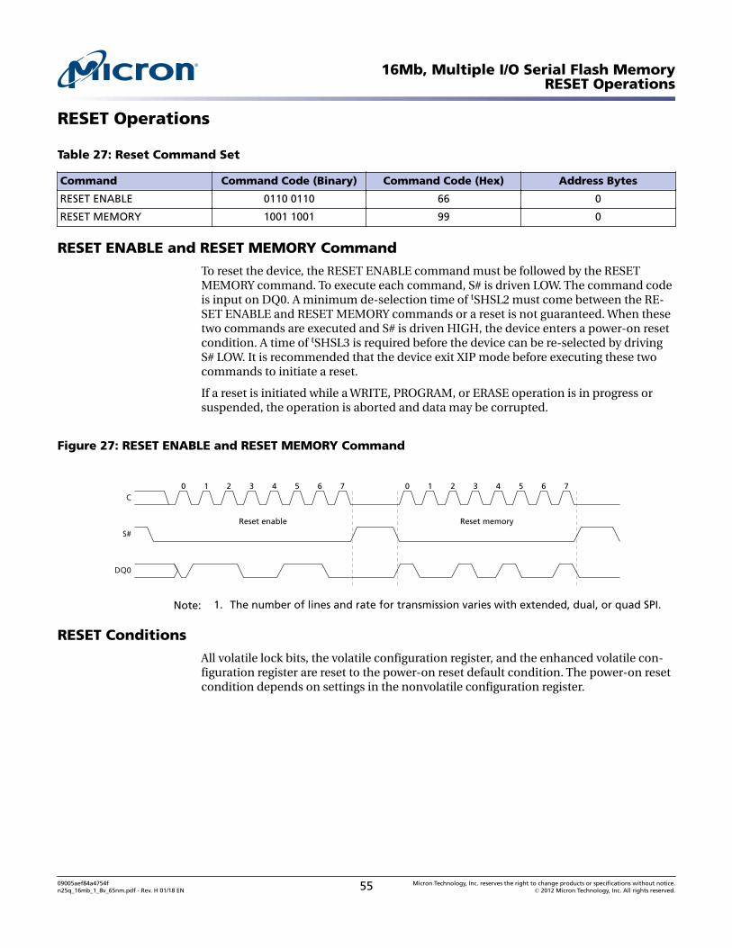
RESET Operations
Table 27: Reset Command Set
Command Command Code (Binary) Command Code (Hex) Address Bytes
RESET ENABLE 0110 0110 66 0
RESET MEMORY 1001 1001 99 0
RESET ENABLE and RESET MEMORY Command
To reset the device, the RESET ENABLE command must be followed by the RESETMEMORY command. To execute each command, S# is driven LOW. The command codeis input on DQ0. A minimum de-selection time of tSHSL2 must come between the RE-SET ENABLE and RESET MEMORY commands or a reset is not guaranteed. When thesetwo commands are executed and S# is driven HIGH, the device enters a power-on resetcondition. A time of tSHSL3 is required before the device can be re-selected by drivingS# LOW. It is recommended that the device exit XIP mode before executing these twocommands to initiate a reset.
If a reset is initiated while a WRITE, PROGRAM, or ERASE operation is in progress orsuspended, the operation is aborted and data may be corrupted.
Figure 27: RESET ENABLE and RESET MEMORY Command
C
S#
DQ0
0 1 2 3 4 5 6 7 0 1 2 3 4 5 6 7
Reset enable Reset memory
Note: 1. The number of lines and rate for transmission varies with extended, dual, or quad SPI.
RESET Conditions
All volatile lock bits, the volatile configuration register, and the enhanced volatile con-figuration register are reset to the power-on reset default condition. The power-on resetcondition depends on settings in the nonvolatile configuration register.
16Mb, Multiple I/O Serial Flash MemoryRESET Operations
09005aef84a4754fn25q_16mb_1_8v_65nm.pdf - Rev. H 01/18 EN 55 Micron Technology, Inc. reserves the right to change products or specifications without notice.
© 2012 Micron Technology, Inc. All rights reserved.
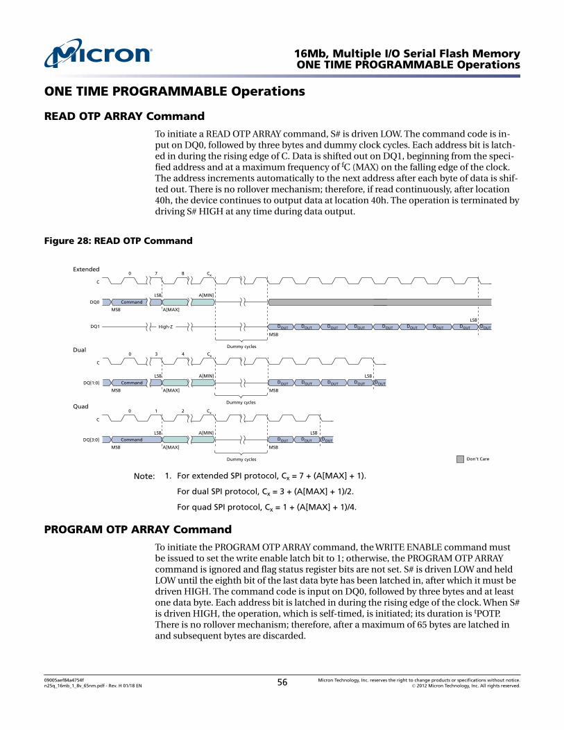
ONE TIME PROGRAMMABLE Operations
READ OTP ARRAY Command
To initiate a READ OTP ARRAY command, S# is driven LOW. The command code is in-put on DQ0, followed by three bytes and dummy clock cycles. Each address bit is latch-ed in during the rising edge of C. Data is shifted out on DQ1, beginning from the speci-fied address and at a maximum frequency of fC (MAX) on the falling edge of the clock.The address increments automatically to the next address after each byte of data is shif-ted out. There is no rollover mechanism; therefore, if read continuously, after location40h, the device continues to output data at location 40h. The operation is terminated bydriving S# HIGH at any time during data output.
Figure 28: READ OTP Command
7 8 Cx0
C
MSB
DQ0
LSB
Command
A[MAX]
A[MIN]
3 4 Cx0
C
MSB
DQ[1:0]
LSB
Command
A[MAX]
A[MIN]
MSB
DOUT DOUT DOUT DOUT DOUT
LSB
Dummy cycles
1 2 Cx0
C
MSB
DQ[3:0]
LSB
Command
A[MAX]
A[MIN]
MSB
DOUT DOUT DOUT
LSB
Dummy cycles
Extended
MSB
DOUT DOUT DOUT DOUT DOUT
LSBDOUT DOUT DOUT DOUT
Dummy cyclesDual
Quad
DQ1 High-Z
Don’t Care
Note: 1. For extended SPI protocol, Cx = 7 + (A[MAX] + 1).
For dual SPI protocol, Cx = 3 + (A[MAX] + 1)/2.
For quad SPI protocol, Cx = 1 + (A[MAX] + 1)/4.
PROGRAM OTP ARRAY Command
To initiate the PROGRAM OTP ARRAY command, the WRITE ENABLE command mustbe issued to set the write enable latch bit to 1; otherwise, the PROGRAM OTP ARRAYcommand is ignored and flag status register bits are not set. S# is driven LOW and heldLOW until the eighth bit of the last data byte has been latched in, after which it must bedriven HIGH. The command code is input on DQ0, followed by three bytes and at leastone data byte. Each address bit is latched in during the rising edge of the clock. When S#is driven HIGH, the operation, which is self-timed, is initiated; its duration is tPOTP.There is no rollover mechanism; therefore, after a maximum of 65 bytes are latched inand subsequent bytes are discarded.
16Mb, Multiple I/O Serial Flash MemoryONE TIME PROGRAMMABLE Operations
09005aef84a4754fn25q_16mb_1_8v_65nm.pdf - Rev. H 01/18 EN 56 Micron Technology, Inc. reserves the right to change products or specifications without notice.
© 2012 Micron Technology, Inc. All rights reserved.
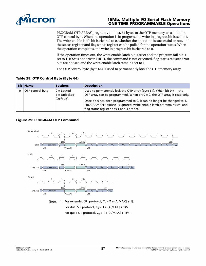
PROGRAM OTP ARRAY programs, at most, 64 bytes to the OTP memory area and oneOTP control byte. When the operation is in progress, the write in progress bit is set to 1.The write enable latch bit is cleared to 0, whether the operation is successful or not, andthe status register and flag status register can be polled for the operation status. Whenthe operation completes, the write in progress bit is cleared to 0.
If the operation times out, the write enable latch bit is reset and the program fail bit isset to 1. If S# is not driven HIGH, the command is not executed, flag status register errorbits are not set, and the write enable latch remains set to 1.
The OTP control byte (byte 64) is used to permanently lock the OTP memory array.
Table 28: OTP Control Byte (Byte 64)
Bit Name Settings Description
0 OTP control byte 0 = Locked1 = Unlocked(Default)
Used to permanently lock the OTP array (byte 64). When bit 0 = 1, theOTP array can be programmed. When bit 0 = 0, the OTP array is read only.
Once bit 0 has been programmed to 0, it can no longer be changed to 1.PROGRAM OTP ARRAY is ignored, write enable latch bit remains set, andflag status register bits 1 and 4 are set.
Figure 29: PROGRAM OTP Command
7 8 Cx0
C
MSB
DQ0
LSB
Command
A[MAX]
A[MIN]
MSB
DIN DIN DIN DIN DIN
LSBDIN DIN DIN DIN
3 4 Cx0
C
MSB
DQ[1:0]
LSB
Command
A[MAX]
A[MIN]
MSB
DIN DIN DIN DIN DIN
LSB
1 2 Cx0
C
MSB
DQ[3:0]
LSB
Command
A[MAX]
A[MIN]
MSB
DIN DIN DIN
LSB
Extended
Dual
Quad
Note: 1. For extended SPI protocol, Cx = 7 + (A[MAX] + 1).
For dual SPI protocol, Cx = 3 + (A[MAX] + 1)/2.
For quad SPI protocol, Cx = 1 + (A[MAX] + 1)/4.
16Mb, Multiple I/O Serial Flash MemoryONE TIME PROGRAMMABLE Operations
09005aef84a4754fn25q_16mb_1_8v_65nm.pdf - Rev. H 01/18 EN 57 Micron Technology, Inc. reserves the right to change products or specifications without notice.
© 2012 Micron Technology, Inc. All rights reserved.
XIP ModeExecute-in-place (XIP) mode allows the memory to be read by sending an address to thedevice and then receiving the data on one, two, or four pins in parallel, depending onthe customer requirements. XIP mode offers maximum flexibility to the application,saves instruction overhead, and reduces random access time.
Activate or Terminate XIP Using Volatile Configuration Register
Applications that boot in SPI and must switch to XIP use the volatile configuration reg-ister. XIP provides faster memory READ operations by requiring only an address to exe-cute, rather than a command code and an address.
To activate XIP requires two steps. First, enable XIP by setting volatile configuration reg-ister bit 3 to 0. Next, drive the XIP confirmation bit to 0 during the next FAST READ op-eration. XIP is then active. Once in XIP, any command that occurs after S# is toggled re-quires only address bits to execute; a command code is not necessary, and device oper-ations use the SPI protocol that is enabled. XIP is terminated by driving the XIP confir-mation bit to 1. The device automatically resets volatile configuration register bit 3 to 1.
Note: For devices with basic XIP, indicated by a part number feature set digit of 2 or 4, itis not necessary to set the volatile configuration register bit 3 to 0 to enable XIP. Instead,it is enabled by setting the XIP confirmation bit to 0 during the first dummy clock cycleafter any FAST READ command.
Activate or Terminate XIP Using Nonvolatile Configuration Register
Applications that must boot directly in XIP use the nonvolatile configuration register. Toenable a device to power-up in XIP using the nonvolatile configuration register, set non-volatile configuration register bits [11:9]. Settings vary according to protocol, as ex-plained in the Nonvolatile Configuration Register section. Because the device boots di-rectly in XIP, the confirmation bit is already set to 0, and after the next power cycle, XIPis active. Once in XIP, a command code is unnecessary, and device operations use theSPI protocol currently enabled. XIP is terminated by driving the XIP confirmation bit to1.
16Mb, Multiple I/O Serial Flash MemoryXIP Mode
09005aef84a4754fn25q_16mb_1_8v_65nm.pdf - Rev. H 01/18 EN 58 Micron Technology, Inc. reserves the right to change products or specifications without notice.
© 2012 Micron Technology, Inc. All rights reserved.
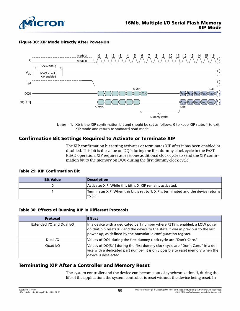
Figure 30: XIP Mode Directly After Power-On
C
VCC
S#
DQ0
DQ[3:1]
DOUTXb DOUT DOUT DOUT DOUT
DOUT DOUT DOUT DOUT DOUT
0 1 2 3 4 5 6 7 8 9 10 11 12 13 14 15 16
tVSI (<100µ)
NVCR check:XIP enabled
Dummy cycles
Mode 3
Mode 0
A[MAX] MSB
A[MIN] LSB
Note: 1. Xb is the XIP confirmation bit and should be set as follows: 0 to keep XIP state; 1 to exitXIP mode and return to standard read mode.
Confirmation Bit Settings Required to Activate or Terminate XIP
The XIP confirmation bit setting activates or terminates XIP after it has been enabled ordisabled. This bit is the value on DQ0 during the first dummy clock cycle in the FASTREAD operation. XIP requires at least one additional clock cycle to send the XIP confir-mation bit to the memory on DQ0 during the first dummy clock cycle.
Table 29: XIP Confirmation Bit
Bit Value Description
0 Activates XIP: While this bit is 0, XIP remains activated.
1 Terminates XIP: When this bit is set to 1, XIP is terminated and the device returnsto SPI.
Table 30: Effects of Running XIP in Different Protocols
Protocol Effect
Extended I/O and Dual I/O In a device with a dedicated part number where RST# is enabled, a LOW pulseon that pin resets XIP and the device to the state it was in previous to the lastpower-up, as defined by the nonvolatile configuration register.
Dual I/O Values of DQ1 during the first dummy clock cycle are "Don't Care."
Quad I/O Values of DQ[3:1] during the first dummy clock cycle are "Don't Care." In a de-vice with a dedicated part number, it is only possible to reset memory when thedevice is deselected.
Terminating XIP After a Controller and Memory Reset
The system controller and the device can become out of synchronization if, during thelife of the application, the system controller is reset without the device being reset. In
16Mb, Multiple I/O Serial Flash MemoryXIP Mode
09005aef84a4754fn25q_16mb_1_8v_65nm.pdf - Rev. H 01/18 EN 59 Micron Technology, Inc. reserves the right to change products or specifications without notice.
© 2012 Micron Technology, Inc. All rights reserved.
such a case, the controller can reset the memory to power-on reset if the memory hasreset functionality. (Reset is available in devices with a dedicated part number.)
If reset functionality is not available, has been disabled, or is not supported by the con-troller, the controller must execute the following sequence to terminate XIP in thememory device. In quad I/O protocol, drive DQ0 = 1 with S# held LOW for seven clockcycles; S# must driven HIGH before the eighth clock cycle. In dual I/O protocol, driveDQ0 = 1 with S# held LOW for 13 clock cycles; S# must driven HIGH before the four-teenth clock cycle. If the device is in extended protocol, drive DQ0 = 1 with S# held LOWfor 25 clock cycles; S# must driven HIGH before the twenty-sixth clock cycle.
These sequences cause the controller to set the XIP confirmation bit to 1, thereby termi-nating XIP. However, it does not reset the device or interrupt PROGRAM/ERASE opera-tions that may be in progress. After terminating XIP, the controller must execute RESETENABLE and RESET MEMORY to implement a software reset and reset the device.
16Mb, Multiple I/O Serial Flash MemoryXIP Mode
09005aef84a4754fn25q_16mb_1_8v_65nm.pdf - Rev. H 01/18 EN 60 Micron Technology, Inc. reserves the right to change products or specifications without notice.
© 2012 Micron Technology, Inc. All rights reserved.
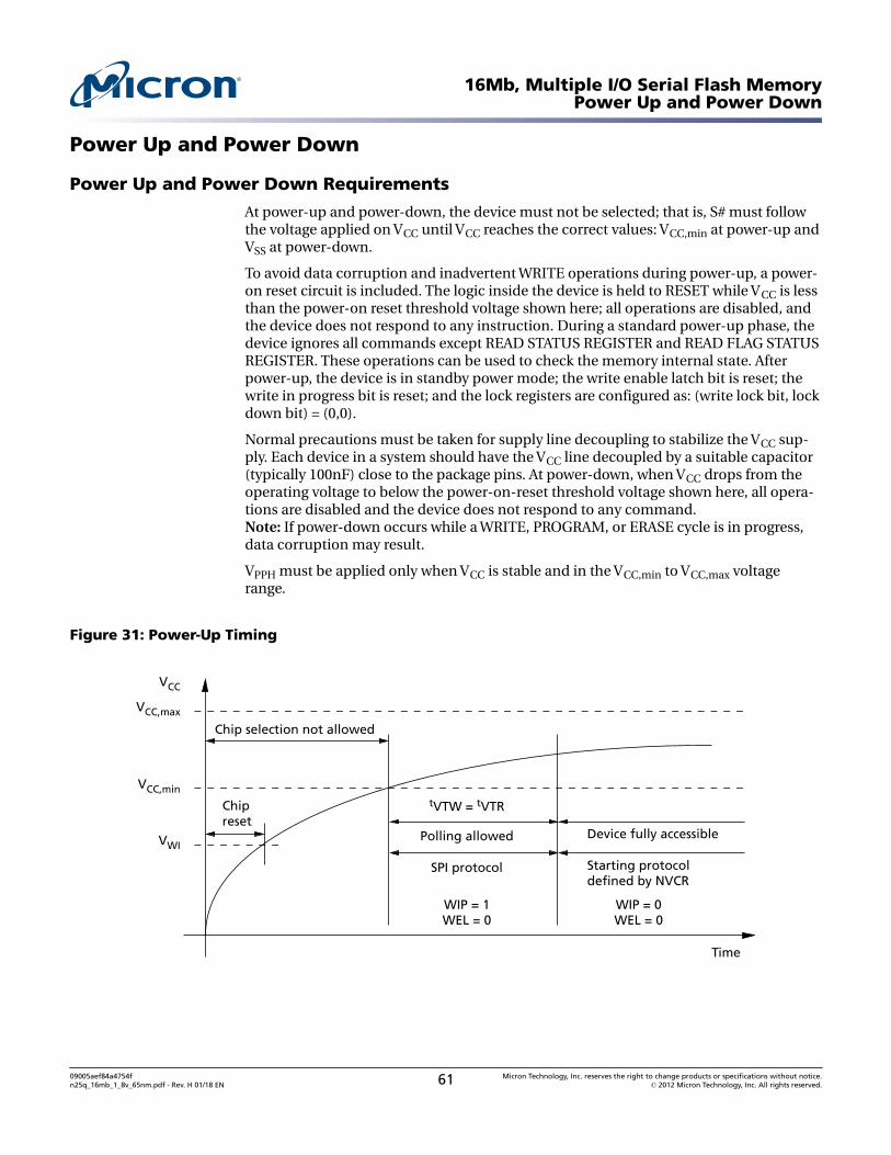
Power Up and Power Down
Power Up and Power Down Requirements
At power-up and power-down, the device must not be selected; that is, S# must followthe voltage applied on VCC until VCC reaches the correct values: VCC,min at power-up andVSS at power-down.
To avoid data corruption and inadvertent WRITE operations during power-up, a power-on reset circuit is included. The logic inside the device is held to RESET while VCC is lessthan the power-on reset threshold voltage shown here; all operations are disabled, andthe device does not respond to any instruction. During a standard power-up phase, thedevice ignores all commands except READ STATUS REGISTER and READ FLAG STATUSREGISTER. These operations can be used to check the memory internal state. Afterpower-up, the device is in standby power mode; the write enable latch bit is reset; thewrite in progress bit is reset; and the lock registers are configured as: (write lock bit, lockdown bit) = (0,0).
Normal precautions must be taken for supply line decoupling to stabilize the VCC sup-ply. Each device in a system should have the VCC line decoupled by a suitable capacitor(typically 100nF) close to the package pins. At power-down, when VCC drops from theoperating voltage to below the power-on-reset threshold voltage shown here, all opera-tions are disabled and the device does not respond to any command.Note: If power-down occurs while a WRITE, PROGRAM, or ERASE cycle is in progress,data corruption may result.
VPPH must be applied only when VCC is stable and in the VCC,min to VCC,max voltagerange.
Figure 31: Power-Up Timing
VCC
VCC,min
VWI
Chipreset
Chip selection not allowed
Polling allowed
tVTW = tVTR
Time
Device fully accessible
VCC,max
SPI protocol Starting protocoldefined by NVCR
WIP = 1WEL = 0
WIP = 0WEL = 0
16Mb, Multiple I/O Serial Flash MemoryPower Up and Power Down
09005aef84a4754fn25q_16mb_1_8v_65nm.pdf - Rev. H 01/18 EN 61 Micron Technology, Inc. reserves the right to change products or specifications without notice.
© 2012 Micron Technology, Inc. All rights reserved.
Table 31: Power-Up Timing and VWI Threshold
Note 1 applies to entire tableSymbol Parameter Min Max Unit
tVTR VCC,min to read – 150 µstVTW VCC,min to device fully accessible – 150 µs
VWI Write inhibit voltage 1.3 1.5 V
Note: 1. Parameters listed are characterized only.
Power Loss Recovery Sequence
If a power loss occurs during a WRITE NONVOLATILE CONFIGURATION REGISTERcommand, after the next power-on, the device might begin in an undetermined state(XIP mode or an unnecessary protocol). If this occurs, until the next power-up, a recov-ery sequence must reset the device to a fixed state (extended SPI protocol without XIP).After the recovery sequence, the issue should be resolved definitively by running theWRITE NONVOLATILE CONFIGURATION REGISTER command again. The recovery se-quence is composed of two parts that must be run in the correct order. During the en-tire sequence, tSHSL2 must be at least 50ns. The first part of the sequence is DQ0 (PADDATA) equal to 1 for the situations listed below:
• 7 clock cycles within S# LOW (S# becomes HIGH before 8th clock cycle)• + 13 clock cycles within S# LOW (S# becomes HIGH before 14th clock cycle)• + 25 clock cycles within S# LOW (S# becomes HIGH before 26th clock cycle)
The second part of the sequence is exiting from dual or quad SPI protocol by using thefollowing FFh sequence: DQ0 (PAD DATA) and DQ3 (PAD HOLD) equal to 1 for 8 clockcycles within S# LOW; S# becomes HIGH before 9th clock cycle.
After this two-part sequence the extended SPI protocol is active.
16Mb, Multiple I/O Serial Flash MemoryPower Up and Power Down
09005aef84a4754fn25q_16mb_1_8v_65nm.pdf - Rev. H 01/18 EN 62 Micron Technology, Inc. reserves the right to change products or specifications without notice.
© 2012 Micron Technology, Inc. All rights reserved.
AC Reset Specifications
Table 32: AC RESET Conditions
Note 1 applies to entire tableParameter Symbol Conditions Min Typ Max Unit
Reset pulsewidth
tRLRH, 2 – 50 – – ns
Reset recoverytime
tRHSL S# HIGH deselects device: XIP mode – – 40 ns
S# HIGH deselects device: standby mode – – 40 ns
S# HIGH deselects device: deep power-down mode – – 30 µs
Commands are being decoded, any READ operations arein progress or any WRITE operation to volatile registersare in progress
– – 40 ns
Any device array PROGRAM/ERASE/SUSPEND/RESUME,PROGRAM OTP, NONVOLATILE SECTOR LOCK, and ERASENONVOLATILE SECTOR LOCK ARRAY operations are inprogress
– – 30 µs
While a WRITE STATUS REGISTER operation is in progress – tW – s
While a WRITE NONVOLATILE CONFIGURATION REGIS-TER operation is in progress
– tWNVCR – ms
On completion or suspension of a SUBSECTOR ERASE(4KB) operation
– tSSE1 – s
On completion or suspension of a SUBSECTOR ERASE(32KB) operation
– tSSE2 – s
Software resetrecovery time
tSHSL3 S# HIGH deselects device: standby mode – – 90 ns
S# HIGH deselects device: deep power-down mode 30 µs
On completion of any Flash array PROGRAM/ERASE/SUSPEND/RESUME, SECTOR ERASE, PROGRAM OTP, PAGEPROGRAM, DUAL INPUT FAST PROGRAM, EXTENDEDDUAL INPUT FAST PROGRAM, QUAD INPUT FAST PRO-GRAM, or EXTENDED QUAD INPUT FAST PROGRAM op-eration
– – 30 µs
On completion or suspension of a WRITE STATUS REGIS-TER operation
– tW – ms
On completion or suspension of a WRITE NONVOLATILECONFIGURATION REGISTER operation
– tWNVCR – s
On completion or suspension of a SUBSECTOR ERASE(4KB) operation
– tSSE1 – s
On completion or suspension of a SUBSECTOR ERASE(32KB) operation
– tSSE2 – s
S# deselect toreset valid
tSHRV Deselect to reset valid in quad output or in QIO-SPI 2 – – ns
Notes: 1. Values are guaranteed by characterization; not 100% tested.2. The device reset is possible but not guaranteed if tRLRH < 50ns.
16Mb, Multiple I/O Serial Flash MemoryAC Reset Specifications
09005aef84a4754fn25q_16mb_1_8v_65nm.pdf - Rev. H 01/18 EN 63 Micron Technology, Inc. reserves the right to change products or specifications without notice.
© 2012 Micron Technology, Inc. All rights reserved.
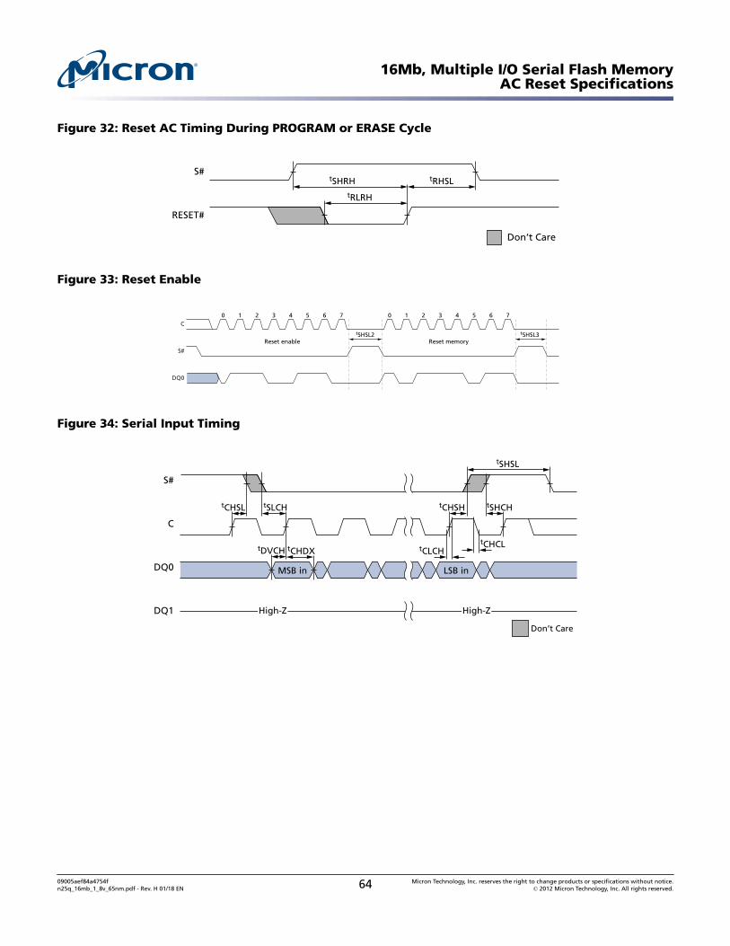
Figure 32: Reset AC Timing During PROGRAM or ERASE Cycle
tSHRHtRLRH
tRHSLS#
RESET#
Don’t Care
Figure 33: Reset Enable
C
S#
DQ0
0 1 2 3 4 5 6 7 0 1 2 3 4 5 6 7
Reset enable Reset memorytSHSL2 tSHSL3
Figure 34: Serial Input Timing
tSLCHtCHSL
tDVCH tCHDX tCLCHtCHCL
tCHSH tSHCH
tSHSL
S#
C
DQ0
DQ1 High-Z High-Z
MSB in LSB in
Don’t Care
16Mb, Multiple I/O Serial Flash MemoryAC Reset Specifications
09005aef84a4754fn25q_16mb_1_8v_65nm.pdf - Rev. H 01/18 EN 64 Micron Technology, Inc. reserves the right to change products or specifications without notice.
© 2012 Micron Technology, Inc. All rights reserved.
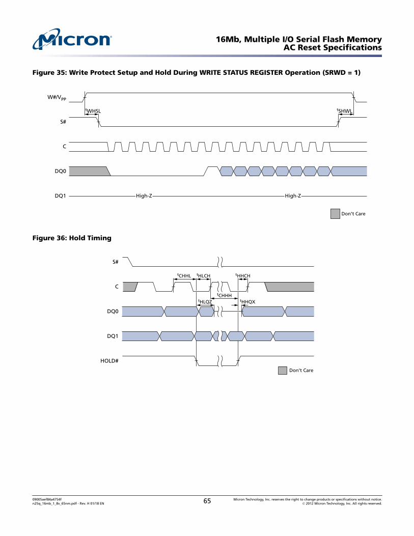
Figure 35: Write Protect Setup and Hold During WRITE STATUS REGISTER Operation (SRWD = 1)
Don’t Care
High-Z High-Z
W#/VPP
S#
C
DQ0
DQ1
tWHSL tSHWL
Figure 36: Hold Timing
tHLCHtCHHL tHHCH
tHLQZ
tCHHHtHHQX
S#
C
DQ0
DQ1
HOLD#
Don’t Care
16Mb, Multiple I/O Serial Flash MemoryAC Reset Specifications
09005aef84a4754fn25q_16mb_1_8v_65nm.pdf - Rev. H 01/18 EN 65 Micron Technology, Inc. reserves the right to change products or specifications without notice.
© 2012 Micron Technology, Inc. All rights reserved.
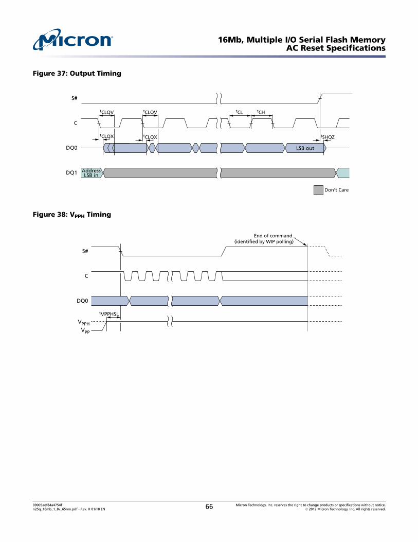
Figure 37: Output Timing
tCL tCH
S#
C
DQ0
DQ1
LSB out
AddressLSB in
Don’t Care
tCLQX tCLQX tSHQZ
tCLQV tCLQV
Figure 38: VPPH Timing
S#
C
DQ0
tVPPHSL
End of command (identified by WIP polling)
VPPHVPP
16Mb, Multiple I/O Serial Flash MemoryAC Reset Specifications
09005aef84a4754fn25q_16mb_1_8v_65nm.pdf - Rev. H 01/18 EN 66 Micron Technology, Inc. reserves the right to change products or specifications without notice.
© 2012 Micron Technology, Inc. All rights reserved.
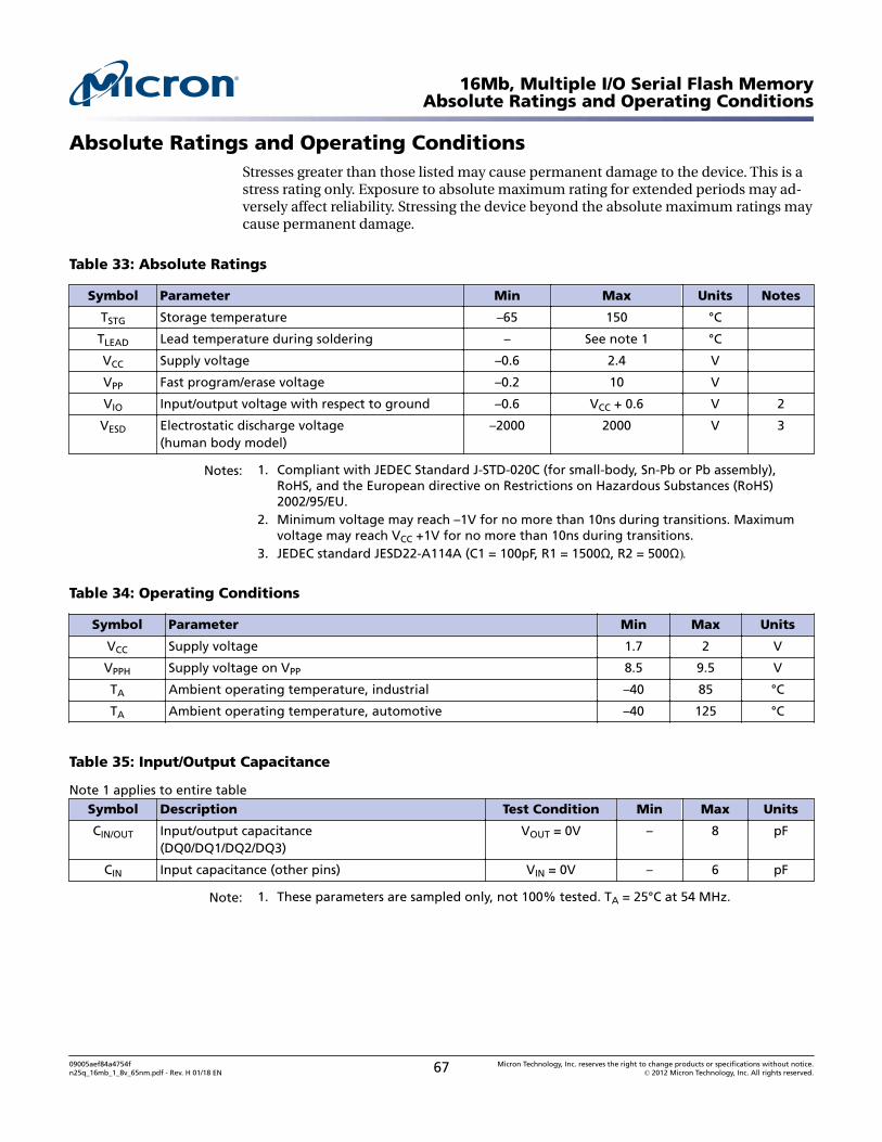
Absolute Ratings and Operating ConditionsStresses greater than those listed may cause permanent damage to the device. This is astress rating only. Exposure to absolute maximum rating for extended periods may ad-versely affect reliability. Stressing the device beyond the absolute maximum ratings maycause permanent damage.
Table 33: Absolute Ratings
Symbol Parameter Min Max Units Notes
TSTG Storage temperature –65 150 °C
TLEAD Lead temperature during soldering – See note 1 °C
VCC Supply voltage –0.6 2.4 V
VPP Fast program/erase voltage –0.2 10 V
VIO Input/output voltage with respect to ground –0.6 VCC + 0.6 V 2
VESD Electrostatic discharge voltage(human body model)
–2000 2000 V 3
Notes: 1. Compliant with JEDEC Standard J-STD-020C (for small-body, Sn-Pb or Pb assembly),RoHS, and the European directive on Restrictions on Hazardous Substances (RoHS)2002/95/EU.
2. Minimum voltage may reach –1V for no more than 10ns during transitions. Maximumvoltage may reach VCC +1V for no more than 10ns during transitions.
3. JEDEC standard JESD22-A114A (C1 = 100pF, R1 = 1500Ω, R2 = 500Ω).
Table 34: Operating Conditions
Symbol Parameter Min Max Units
VCC Supply voltage 1.7 2 V
VPPH Supply voltage on VPP 8.5 9.5 V
TA Ambient operating temperature, industrial –40 85 °C
TA Ambient operating temperature, automotive –40 125 °C
Table 35: Input/Output Capacitance
Note 1 applies to entire tableSymbol Description Test Condition Min Max Units
CIN/OUT Input/output capacitance(DQ0/DQ1/DQ2/DQ3)
VOUT = 0V – 8 pF
CIN Input capacitance (other pins) VIN = 0V – 6 pF
Note: 1. These parameters are sampled only, not 100% tested. TA = 25°C at 54 MHz.
16Mb, Multiple I/O Serial Flash MemoryAbsolute Ratings and Operating Conditions
09005aef84a4754fn25q_16mb_1_8v_65nm.pdf - Rev. H 01/18 EN 67 Micron Technology, Inc. reserves the right to change products or specifications without notice.
© 2012 Micron Technology, Inc. All rights reserved.
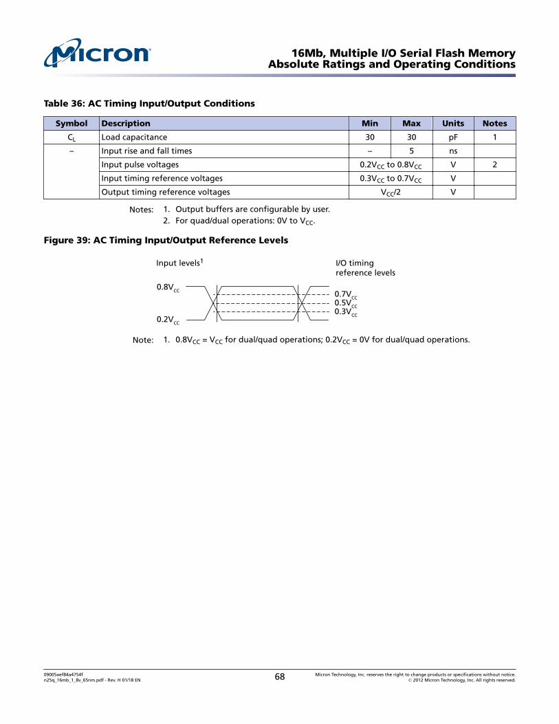
Table 36: AC Timing Input/Output Conditions
Symbol Description Min Max Units Notes
CL Load capacitance 30 30 pF 1
– Input rise and fall times – 5 ns
Input pulse voltages 0.2VCC to 0.8VCC V 2
Input timing reference voltages 0.3VCC to 0.7VCC V
Output timing reference voltages VCC/2 V
Notes: 1. Output buffers are configurable by user.2. For quad/dual operations: 0V to VCC.
Figure 39: AC Timing Input/Output Reference Levels
0.8VCC
0.2VCC
0.7VCC0.5VCC0.3VCC
Input levels1 I/O timingreference levels
Note: 1. 0.8VCC = VCC for dual/quad operations; 0.2VCC = 0V for dual/quad operations.
16Mb, Multiple I/O Serial Flash MemoryAbsolute Ratings and Operating Conditions
09005aef84a4754fn25q_16mb_1_8v_65nm.pdf - Rev. H 01/18 EN 68 Micron Technology, Inc. reserves the right to change products or specifications without notice.
© 2012 Micron Technology, Inc. All rights reserved.
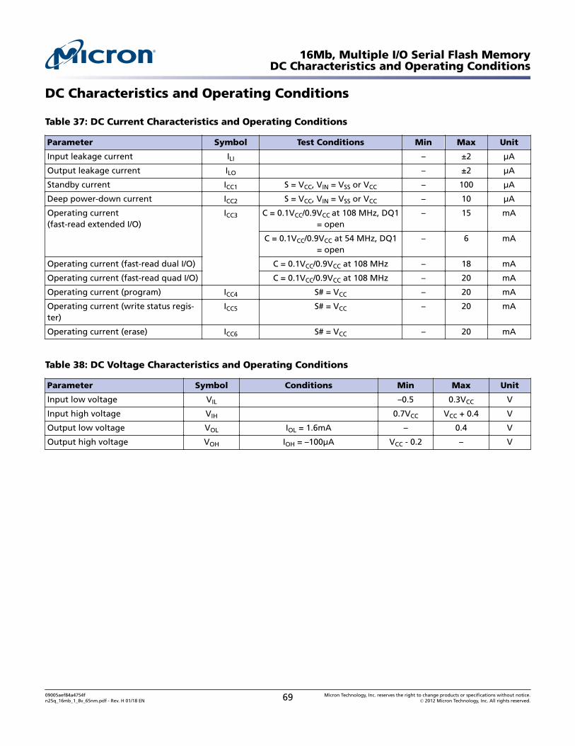
DC Characteristics and Operating Conditions
Table 37: DC Current Characteristics and Operating Conditions
Parameter Symbol Test Conditions Min Max Unit
Input leakage current ILI – ±2 µA
Output leakage current ILO – ±2 µA
Standby current ICC1 S = VCC, VIN = VSS or VCC – 100 µA
Deep power-down current ICC2 S = VCC, VIN = VSS or VCC – 10 µA
Operating current(fast-read extended I/O)
ICC3 C = 0.1VCC/0.9VCC at 108 MHz, DQ1= open
– 15 mA
C = 0.1VCC/0.9VCC at 54 MHz, DQ1= open
– 6 mA
Operating current (fast-read dual I/O) C = 0.1VCC/0.9VCC at 108 MHz – 18 mA
Operating current (fast-read quad I/O) C = 0.1VCC/0.9VCC at 108 MHz – 20 mA
Operating current (program) ICC4 S# = VCC – 20 mA
Operating current (write status regis-ter)
ICC5 S# = VCC – 20 mA
Operating current (erase) ICC6 S# = VCC – 20 mA
Table 38: DC Voltage Characteristics and Operating Conditions
Parameter Symbol Conditions Min Max Unit
Input low voltage VIL –0.5 0.3VCC V
Input high voltage VIH 0.7VCC VCC + 0.4 V
Output low voltage VOL IOL = 1.6mA – 0.4 V
Output high voltage VOH IOH = –100µA VCC - 0.2 – V
16Mb, Multiple I/O Serial Flash MemoryDC Characteristics and Operating Conditions
09005aef84a4754fn25q_16mb_1_8v_65nm.pdf - Rev. H 01/18 EN 69 Micron Technology, Inc. reserves the right to change products or specifications without notice.
© 2012 Micron Technology, Inc. All rights reserved.
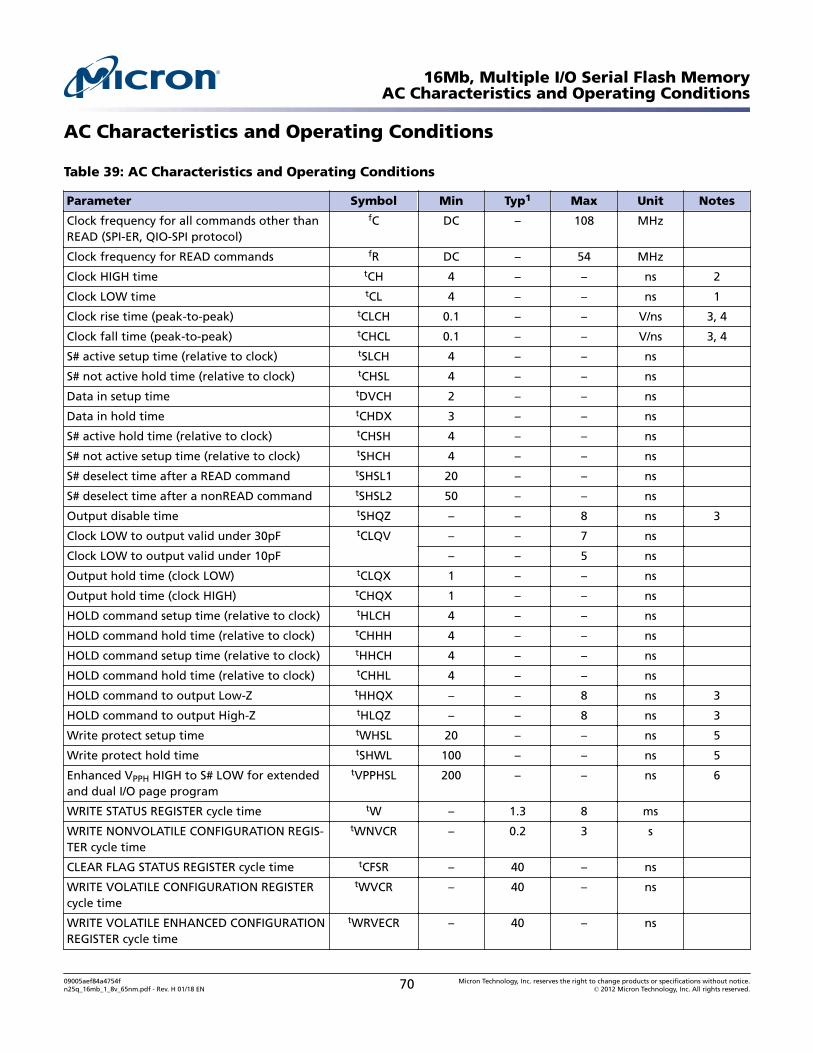
AC Characteristics and Operating Conditions
Table 39: AC Characteristics and Operating Conditions
Parameter Symbol Min Typ1 Max Unit Notes
Clock frequency for all commands other thanREAD (SPI-ER, QIO-SPI protocol)
fC DC – 108 MHz
Clock frequency for READ commands fR DC – 54 MHz
Clock HIGH time tCH 4 – – ns 2
Clock LOW time tCL 4 – – ns 1
Clock rise time (peak-to-peak) tCLCH 0.1 – – V/ns 3, 4
Clock fall time (peak-to-peak) tCHCL 0.1 – – V/ns 3, 4
S# active setup time (relative to clock) tSLCH 4 – – ns
S# not active hold time (relative to clock) tCHSL 4 – – ns
Data in setup time tDVCH 2 – – ns
Data in hold time tCHDX 3 – – ns
S# active hold time (relative to clock) tCHSH 4 – – ns
S# not active setup time (relative to clock) tSHCH 4 – – ns
S# deselect time after a READ command tSHSL1 20 – – ns
S# deselect time after a nonREAD command tSHSL2 50 – – ns
Output disable time tSHQZ – – 8 ns 3
Clock LOW to output valid under 30pF tCLQV – – 7 ns
Clock LOW to output valid under 10pF – – 5 ns
Output hold time (clock LOW) tCLQX 1 – – ns
Output hold time (clock HIGH) tCHQX 1 – – ns
HOLD command setup time (relative to clock) tHLCH 4 – – ns
HOLD command hold time (relative to clock) tCHHH 4 – – ns
HOLD command setup time (relative to clock) tHHCH 4 – – ns
HOLD command hold time (relative to clock) tCHHL 4 – – ns
HOLD command to output Low-Z tHHQX – – 8 ns 3
HOLD command to output High-Z tHLQZ – – 8 ns 3
Write protect setup time tWHSL 20 – – ns 5
Write protect hold time tSHWL 100 – – ns 5
Enhanced VPPH HIGH to S# LOW for extendedand dual I/O page program
tVPPHSL 200 – – ns 6
WRITE STATUS REGISTER cycle time tW – 1.3 8 ms
WRITE NONVOLATILE CONFIGURATION REGIS-TER cycle time
tWNVCR – 0.2 3 s
CLEAR FLAG STATUS REGISTER cycle time tCFSR – 40 – ns
WRITE VOLATILE CONFIGURATION REGISTERcycle time
tWVCR – 40 – ns
WRITE VOLATILE ENHANCED CONFIGURATIONREGISTER cycle time
tWRVECR – 40 – ns
16Mb, Multiple I/O Serial Flash MemoryAC Characteristics and Operating Conditions
09005aef84a4754fn25q_16mb_1_8v_65nm.pdf - Rev. H 01/18 EN 70 Micron Technology, Inc. reserves the right to change products or specifications without notice.
© 2012 Micron Technology, Inc. All rights reserved.
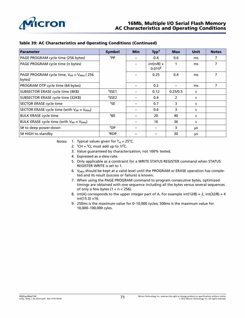
Table 39: AC Characteristics and Operating Conditions (Continued)
Parameter Symbol Min Typ1 Max Unit Notes
PAGE PROGRAM cycle time (256 bytes) tPP – 0.4 0.6 ms 7
PAGE PROGRAM cycle time (n bytes) – int(n/8) ×0.0158
1 ms 7
PAGE PROGRAM cycle time, VPP = VPPH ( 256bytes)
– 0.25 0.4 ms 7
PROGRAM OTP cycle time (64 bytes) – 0.2 – ms 7
SUBSECTOR ERASE cycle time (4KB) tSSE1 – 0.12 0.25/0.5 s
SUBSECTOR ERASE cycle time (32KB) tSSE2 – 0.4 2 s
SECTOR ERASE cycle time tSE – 0.7 3 s
SECTOR ERASE cycle time (with VPP = VPPH) – 0.6 3 s
BULK ERASE cycle time tBE – 20 40 s
BULK ERASE cycle time (with VPP = VPPH) – 16 36 s
S# to deep power-down tDP – – 3 µs
S# HIGH to standby tRDP – – 30 µs
Notes: 1. Typical values given for TA = 25°C.2. tCH + tCL must add up to 1/fC.3. Value guaranteed by characterization; not 100% tested.4. Expressed as a slew-rate.5. Only applicable as a constraint for a WRITE STATUS REGISTER command when STATUS
REGISTER WRITE is set to 1.6. VPPH should be kept at a valid level until the PROGRAM or ERASE operation has comple-
ted and its result (success or failure) is known.7. When using the PAGE PROGRAM command to program consecutive bytes, optimized
timings are obtained with one sequence including all the bytes versus several sequencesof only a few bytes (1 < n < 256).
8. int(A) corresponds to the upper integer part of A. For example int(12/8) = 2, int(32/8) = 4int(15.3) =16.
9. 250ms is the maximum value for 0–10,000 cycles; 500ms is the maximum value for10,000–100,000 cyles.
16Mb, Multiple I/O Serial Flash MemoryAC Characteristics and Operating Conditions
09005aef84a4754fn25q_16mb_1_8v_65nm.pdf - Rev. H 01/18 EN 71 Micron Technology, Inc. reserves the right to change products or specifications without notice.
© 2012 Micron Technology, Inc. All rights reserved.
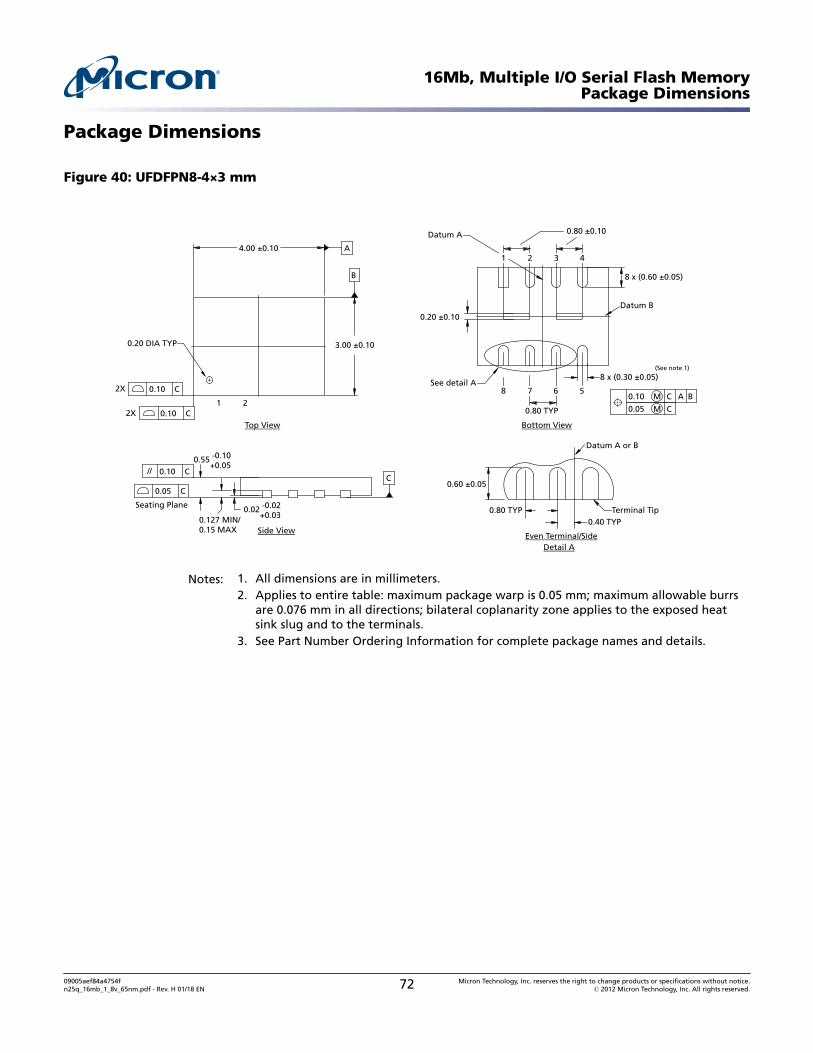
Package Dimensions
Figure 40: UFDFPN8-4×3 mm
Top View
B
A
0.10 C
0.10 C
2X
2X
Bottom View
Side View
C
0.05 C
0.10 C
Seating Plane
0.20 DIA TYP
0.10 C A B
0.05 C
M
M
Datum A
Datum B
See detail A
Even Terminal/Side
Datum A or B
Detail A
Terminal Tip
1 2
0.127 MIN/0.15 MAX
0.80 TYP
0.80 TYP
0.40 TYP
0.02 -0.02+0.03
0.55 -0.10+0.05
//
0.60 ±0.05
8 x (0.30 ±0.05)
0.20 ±0.10
4.00 ±0.10
0.80 ±0.10
8 x (0.60 ±0.05)
3.00 ±0.10
2 3 41
5678
(See note 1)
Notes: 1. All dimensions are in millimeters.2. Applies to entire table: maximum package warp is 0.05 mm; maximum allowable burrs
are 0.076 mm in all directions; bilateral coplanarity zone applies to the exposed heatsink slug and to the terminals.
3. See Part Number Ordering Information for complete package names and details.
16Mb, Multiple I/O Serial Flash MemoryPackage Dimensions
09005aef84a4754fn25q_16mb_1_8v_65nm.pdf - Rev. H 01/18 EN 72 Micron Technology, Inc. reserves the right to change products or specifications without notice.
© 2012 Micron Technology, Inc. All rights reserved.
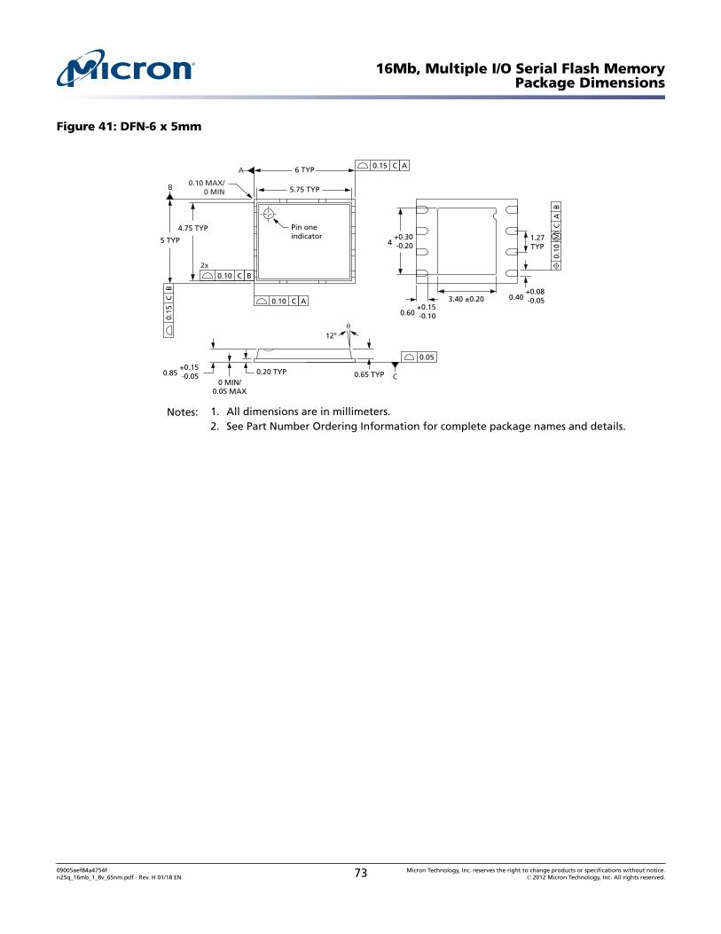
Figure 41: DFN-6 x 5mm
12°
0.20 TYP0 MIN/
0.05 MAX
5.75 TYP
Pin oneindicator 1.27
TYP4 +0.30-0.20
0.60 +0.15-0.10
0.85 +0.15-0.05
0.40 +0.08-0.053.40 ±0.20
θ
0.10 MAX/0 MIN
C
A
B
M
2x
6 TYP
4.75 TYP
0.05
5 TYP
0.65 TYP
0.10 C B
0.10 C A
0.15
CB
0.10
CA
B
0.15 C A
Notes: 1. All dimensions are in millimeters.2. See Part Number Ordering Information for complete package names and details.
16Mb, Multiple I/O Serial Flash MemoryPackage Dimensions
09005aef84a4754fn25q_16mb_1_8v_65nm.pdf - Rev. H 01/18 EN 73 Micron Technology, Inc. reserves the right to change products or specifications without notice.
© 2012 Micron Technology, Inc. All rights reserved.
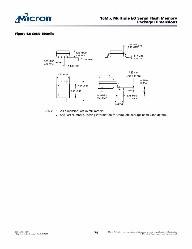
Figure 42: S08N-150mils
8
1
0.25 mmGAUGE PLANE
0.10 MIN/0.25 MAX
0.40 MIN/1.27 MAX
0o MIN/8o MAX
0.28 MIN/0.48 MAX
0.17 MIN/0.23 MAX
x 45°0.25 MIN/0.50 MAX
0.10 MAX
1.75 MAX/
1.27 TYP
1.04 TYP
1.25 MIN
3.90 ±0.10
6.00 ±0.20
4.90 ±0.10
Notes: 1. All dimensions are in millimeters.2. See Part Number Ordering Information for complete package names and details.
16Mb, Multiple I/O Serial Flash MemoryPackage Dimensions
09005aef84a4754fn25q_16mb_1_8v_65nm.pdf - Rev. H 01/18 EN 74 Micron Technology, Inc. reserves the right to change products or specifications without notice.
© 2012 Micron Technology, Inc. All rights reserved.
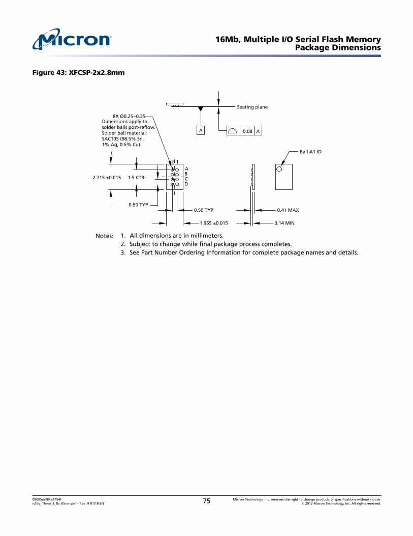
Figure 43: XFCSP-2x2.8mm
Seating plane
0.08 A
12
Ball A1 ID
A
0.14 MIN
0.41 MAX
8X Ø0.25~0.35Dimensions apply tosolder balls post-reflow.Solder ball material:SAC105 (98.5% Sn,1% Ag, 0.5% Cu).
ABCD
1.965 ±0.015
0.50 TYP
1.5 CTR2.715 ±0.015
0.50 TYP
Notes: 1. All dimensions are in millimeters.2. Subject to change while final package process completes.3. See Part Number Ordering Information for complete package names and details.
16Mb, Multiple I/O Serial Flash MemoryPackage Dimensions
09005aef84a4754fn25q_16mb_1_8v_65nm.pdf - Rev. H 01/18 EN 75 Micron Technology, Inc. reserves the right to change products or specifications without notice.
© 2012 Micron Technology, Inc. All rights reserved.
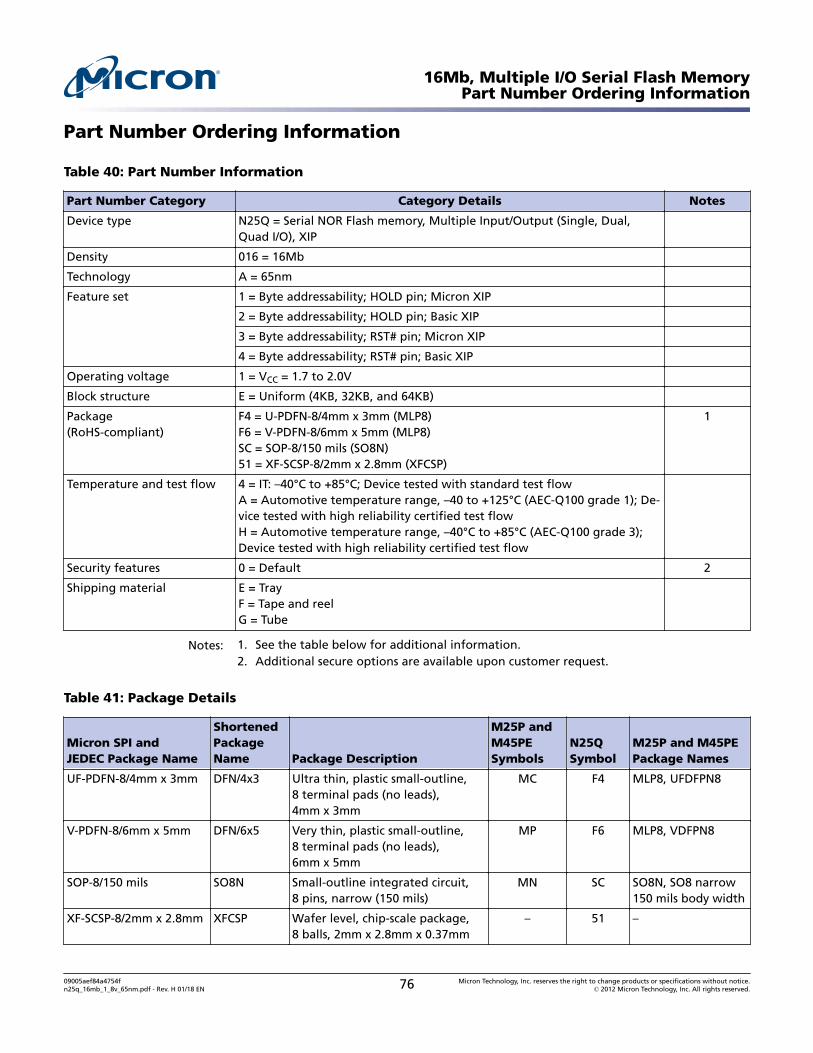
Part Number Ordering Information
Table 40: Part Number Information
Part Number Category Category Details Notes
Device type N25Q = Serial NOR Flash memory, Multiple Input/Output (Single, Dual,Quad I/O), XIP
Density 016 = 16Mb
Technology A = 65nm
Feature set 1 = Byte addressability; HOLD pin; Micron XIP
2 = Byte addressability; HOLD pin; Basic XIP
3 = Byte addressability; RST# pin; Micron XIP
4 = Byte addressability; RST# pin; Basic XIP
Operating voltage 1 = VCC = 1.7 to 2.0V
Block structure E = Uniform (4KB, 32KB, and 64KB)
Package(RoHS-compliant)
F4 = U-PDFN-8/4mm x 3mm (MLP8)F6 = V-PDFN-8/6mm x 5mm (MLP8)SC = SOP-8/150 mils (SO8N)51 = XF-SCSP-8/2mm x 2.8mm (XFCSP)
1
Temperature and test flow 4 = IT: –40°C to +85°C; Device tested with standard test flowA = Automotive temperature range, –40 to +125°C (AEC-Q100 grade 1); De-vice tested with high reliability certified test flowH = Automotive temperature range, –40°C to +85°C (AEC-Q100 grade 3);Device tested with high reliability certified test flow
Security features 0 = Default 2
Shipping material E = TrayF = Tape and reelG = Tube
Notes: 1. See the table below for additional information.2. Additional secure options are available upon customer request.
Table 41: Package Details
Micron SPI andJEDEC Package Name
ShortenedPackageName Package Description
M25P andM45PESymbols
N25QSymbol
M25P and M45PEPackage Names
UF-PDFN-8/4mm x 3mm DFN/4x3 Ultra thin, plastic small-outline,8 terminal pads (no leads),4mm x 3mm
MC F4 MLP8, UFDFPN8
V-PDFN-8/6mm x 5mm DFN/6x5 Very thin, plastic small-outline,8 terminal pads (no leads),6mm x 5mm
MP F6 MLP8, VDFPN8
SOP-8/150 mils SO8N Small-outline integrated circuit,8 pins, narrow (150 mils)
MN SC SO8N, SO8 narrow150 mils body width
XF-SCSP-8/2mm x 2.8mm XFCSP Wafer level, chip-scale package,8 balls, 2mm x 2.8mm x 0.37mm
– 51 –
16Mb, Multiple I/O Serial Flash MemoryPart Number Ordering Information
09005aef84a4754fn25q_16mb_1_8v_65nm.pdf - Rev. H 01/18 EN 76 Micron Technology, Inc. reserves the right to change products or specifications without notice.
© 2012 Micron Technology, Inc. All rights reserved.
Revision History
Rev. H – 2/2018
• Added Important Notes and Warnings section for further clarification aligning to in-dustry standards
Rev. G – 1/2016
• Updated part number in main title• Updated Sequence of Bytes During Wrap table in Nonvolatile and Volatile Registers• Updated Part Number Information table in Part Number Ordering Information
Rev. F – 1/2014
• Corrected RESET ENABLE and RESET MEMORY command timing diagram
Rev. E – 7/2013
• XFCSP package dimension changes
Rev. D – 7/2012
• To Production status
Rev. C – 6/2012
• Updated tSSE specification in AC Reset Conditions table
Rev. B – 5/2012
• Revised figure for 8-Balls, XFCSP, 1.8mm x 2.7mm x 0.37mm (Top View)
Rev. A – 2/2012
• Initial release.
8000 S. Federal Way, P.O. Box 6, Boise, ID 83707-0006, Tel: 208-368-4000www.micron.com/products/support Sales inquiries: 800-932-4992
Micron and the Micron logo are trademarks of Micron Technology, Inc.All other trademarks are the property of their respective owners.
This data sheet contains minimum and maximum limits specified over the power supply and temperature range set forth herein.Although considered final, these specifications are subject to change, as further product development and data characterization some-
times occur.
16Mb, Multiple I/O Serial Flash MemoryRevision History
09005aef84a4754fn25q_16mb_1_8v_65nm.pdf - Rev. H 01/18 EN 77 Micron Technology, Inc. reserves the right to change products or specifications without notice.
© 2012 Micron Technology, Inc. All rights reserved.