micro strip planar array antenna with dgs - ijsrd · more elements patch microstrip antenna array....
TRANSCRIPT
IJSRD - International Journal for Scientific Research & Development| Vol. 2, Issue 09, 2014 | ISSN (online): 2321-0613
All rights reserved by www.ijsrd.com 515
Micro strip Planar Array Antenna with DGS Ankit Mittal1 Ritu Khullar2
1,2Department of Electronics & Communication Engineering
1,2Maharishi Ved Vyas Engineering College, Jagadhri, IndiaAbstract— Antenna is the most important part of wireless
communication. The recent growth in this industry makes
the antenna more advanced and reliable. In various fields we
need the use of highly characteristics antennas and these
characteristics are based upon some parameters like
bandwidth, gain, directivity etc. As compared to other
antennas microstrip antenna can make possible to achieve
the required characteristics for efficient communication
because they are easily to fabricate and reduces the cost
also. To make the microstrip antenna more advanced it use
defected ground structure (DGS). The DGS structures are
introduce to improve the performance of planar array
antenna in terms of return loss, gain, directivity and voltage
standing wave ratio. The goal of this paper is to understand
the mathematical terms of antenna and feeding techniques
so that it possible to know how to make the Microstrip
antenna with DGS as more highly characterized antenna.
Key words: Microstrip array antenna, DGS, antenna
parameters, Feeding & Power divider
I. INTRODUCTION
Microstrip antenna engineering has a history over 60 years
and still we are using it with some improvement for efficient
communication. These antennas play a very important role
in the world of wireless communication systems. There is
always a high demand for great performance, small size and
low cost wireless communication systems. In order to meet
these requirements, microstrip planar patch antenna is
preferred because of their various advantages such as
lightweight, low volume, low cost and ease for fabrication.
Although the microstrip planar patch antenna has various
advantages and also various disadvantages which are like
low gain, narrow bandwidth and low efficiency. These
limitations can be overcome by constructing many patch
antennas in array configuration [1].
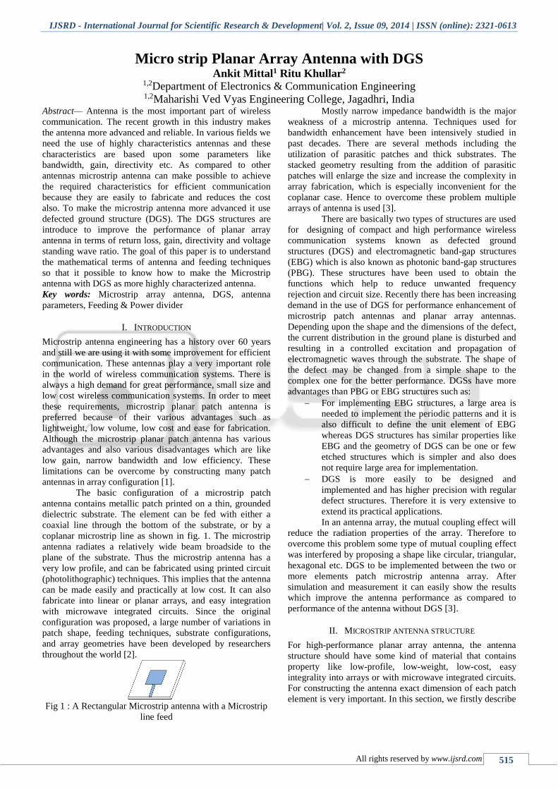
The basic configuration of a microstrip patch
antenna contains metallic patch printed on a thin, grounded
dielectric substrate. The element can be fed with either a
coaxial line through the bottom of the substrate, or by a
coplanar microstrip line as shown in fig. 1. The microstrip
antenna radiates a relatively wide beam broadside to the
plane of the substrate. Thus the microstrip antenna has a
very low profile, and can be fabricated using printed circuit
(photolithographic) techniques. This implies that the antenna
can be made easily and practically at low cost. It can also
fabricate into linear or planar arrays, and easy integration
with microwave integrated circuits. Since the original
configuration was proposed, a large number of variations in
patch shape, feeding techniques, substrate configurations,
and array geometries have been developed by researchers
throughout the world [2].
Fig 1 : A Rectangular Microstrip antenna with a Microstrip
line feed
Mostly narrow impedance bandwidth is the major
weakness of a microstrip antenna. Techniques used for
bandwidth enhancement have been intensively studied in
past decades. There are several methods including the
utilization of parasitic patches and thick substrates. The
stacked geometry resulting from the addition of parasitic
patches will enlarge the size and increase the complexity in
array fabrication, which is especially inconvenient for the
coplanar case. Hence to overcome these problem multiple
arrays of antenna is used [3].
There are basically two types of structures are used
for designing of compact and high performance wireless
communication systems known as defected ground
structures (DGS) and electromagnetic band-gap structures
(EBG) which is also known as photonic band-gap structures
(PBG). These structures have been used to obtain the
functions which help to reduce unwanted frequency
rejection and circuit size. Recently there has been increasing
demand in the use of DGS for performance enhancement of
microstrip patch antennas and planar array antennas.
Depending upon the shape and the dimensions of the defect,
the current distribution in the ground plane is disturbed and
resulting in a controlled excitation and propagation of
electromagnetic waves through the substrate. The shape of
the defect may be changed from a simple shape to the
complex one for the better performance. DGSs have more
advantages than PBG or EBG structures such as:
For implementing EBG structures, a large area is
needed to implement the periodic patterns and it is
also difficult to define the unit element of EBG
whereas DGS structures has similar properties like
EBG and the geometry of DGS can be one or few
etched structures which is simpler and also does
not require large area for implementation.
DGS is more easily to be designed and
implemented and has higher precision with regular
defect structures. Therefore it is very extensive to
extend its practical applications.
In an antenna array, the mutual coupling effect will
reduce the radiation properties of the array. Therefore to
overcome this problem some type of mutual coupling effect
was interfered by proposing a shape like circular, triangular,
hexagonal etc. DGS to be implemented between the two or
more elements patch microstrip antenna array. After
simulation and measurement it can easily show the results
which improve the antenna performance as compared to
performance of the antenna without DGS [3].
II. MICROSTRIP ANTENNA STRUCTURE
For high-performance planar array antenna, the antenna
structure should have some kind of material that contains
property like low-profile, low-weight, low-cost, easy
integrality into arrays or with microwave integrated circuits.
For constructing the antenna exact dimension of each patch
element is very important. In this section, we firstly describe
Micro strip Planar Array Antenna with DGS
(IJSRD/Vol. 2/Issue 09/2014/115)
All rights reserved by www.ijsrd.com 516
the microstrip antenna structure, followed by some DGS
shapes [4].
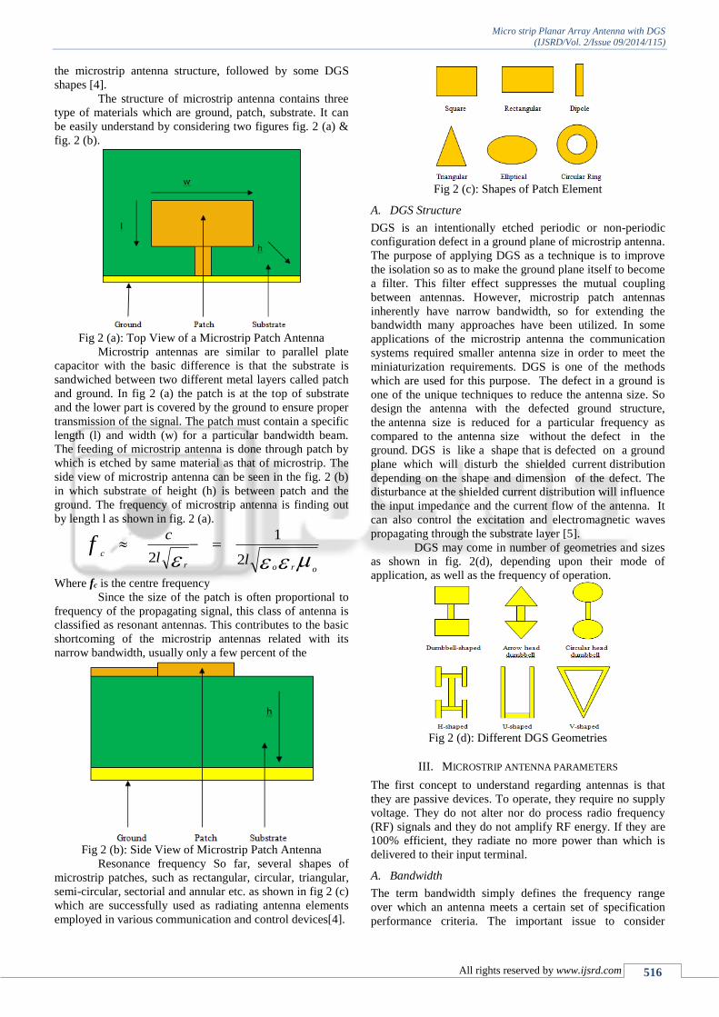
The structure of microstrip antenna contains three
type of materials which are ground, patch, substrate. It can
be easily understand by considering two figures fig. 2 (a) &
fig. 2 (b).
Fig 2 (a): Top View of a Microstrip Patch Antenna
Microstrip antennas are similar to parallel plate
capacitor with the basic difference is that the substrate is
sandwiched between two different metal layers called patch
and ground. In fig 2 (a) the patch is at the top of substrate
and the lower part is covered by the ground to ensure proper
transmission of the signal. The patch must contain a specific
length (l) and width (w) for a particular bandwidth beam.
The feeding of microstrip antenna is done through patch by
which is etched by same material as that of microstrip. The
side view of microstrip antenna can be seen in the fig. 2 (b)
in which substrate of height (h) is between patch and the
ground. The frequency of microstrip antenna is finding out
by length l as shown in fig. 2 (a).
oror
cll
cf
2
1
2
Where fc is the centre frequency
Since the size of the patch is often proportional to
frequency of the propagating signal, this class of antenna is
classified as resonant antennas. This contributes to the basic
shortcoming of the microstrip antennas related with its
narrow bandwidth, usually only a few percent of the
Fig 2 (b): Side View of Microstrip Patch Antenna
Resonance frequency So far, several shapes of
microstrip patches, such as rectangular, circular, triangular,
semi-circular, sectorial and annular etc. as shown in fig 2 (c)
which are successfully used as radiating antenna elements
employed in various communication and control devices[4].
Fig 2 (c): Shapes of Patch Element
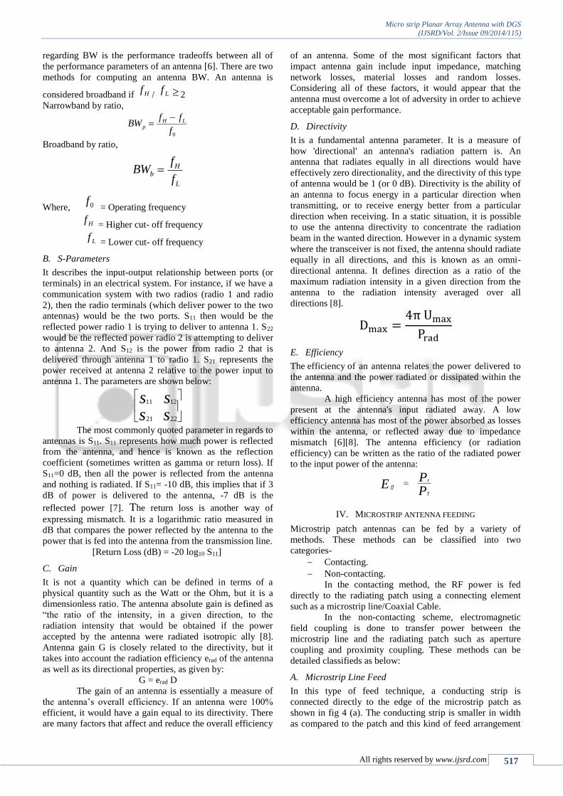
A. DGS Structure
DGS is an intentionally etched periodic or non-periodic
configuration defect in a ground plane of microstrip antenna.
The purpose of applying DGS as a technique is to improve
the isolation so as to make the ground plane itself to become
a filter. This filter effect suppresses the mutual coupling
between antennas. However, microstrip patch antennas
inherently have narrow bandwidth, so for extending the
bandwidth many approaches have been utilized. In some
applications of the microstrip antenna the communication
systems required smaller antenna size in order to meet the
miniaturization requirements. DGS is one of the methods
which are used for this purpose. The defect in a ground is
one of the unique techniques to reduce the antenna size. So
design the antenna with the defected ground structure,
the antenna size is reduced for a particular frequency as
compared to the antenna size without the defect in the
ground. DGS is like a shape that is defected on a ground
plane which will disturb the shielded current distribution
depending on the shape and dimension of the defect. The
disturbance at the shielded current distribution will influence
the input impedance and the current flow of the antenna. It
can also control the excitation and electromagnetic waves
propagating through the substrate layer [5].
DGS may come in number of geometries and sizes
as shown in fig. 2(d), depending upon their mode of
application, as well as the frequency of operation.
Fig 2 (d): Different DGS Geometries
III. MICROSTRIP ANTENNA PARAMETERS
The first concept to understand regarding antennas is that
they are passive devices. To operate, they require no supply
voltage. They do not alter nor do process radio frequency
(RF) signals and they do not amplify RF energy. If they are
100% efficient, they radiate no more power than which is
delivered to their input terminal.
A. Bandwidth
The term bandwidth simply defines the frequency range
over which an antenna meets a certain set of specification
performance criteria. The important issue to consider
Micro strip Planar Array Antenna with DGS
(IJSRD/Vol. 2/Issue 09/2014/115)
All rights reserved by www.ijsrd.com 517
regarding BW is the performance tradeoffs between all of
the performance parameters of an antenna [6]. There are two
methods for computing an antenna BW. An antenna is
considered broadband if Hf/ Lf 2
Narrowband by ratio,
0f
ffBW LH
p
Broadband by ratio,
L
Hb
f
fBW
Where, 0f = Operating frequency
Hf = Higher cut- off frequency
Lf = Lower cut- off frequency
B. S-Parameters
It describes the input-output relationship between ports (or
terminals) in an electrical system. For instance, if we have a
communication system with two radios (radio 1 and radio
2), then the radio terminals (which deliver power to the two
antennas) would be the two ports. S11 then would be the
reflected power radio 1 is trying to deliver to antenna 1. S22
would be the reflected power radio 2 is attempting to deliver
to antenna 2. And S12 is the power from radio 2 that is
delivered through antenna 1 to radio 1. S21 represents the
power received at antenna 2 relative to the power input to
antenna 1. The parameters are shown below:
ssss
2221
1211
The most commonly quoted parameter in regards to
antennas is S11. S11 represents how much power is reflected
from the antenna, and hence is known as the reflection
coefficient (sometimes written as gamma or return loss). If
S11=0 dB, then all the power is reflected from the antenna
and nothing is radiated. If S11= -10 dB, this implies that if 3
dB of power is delivered to the antenna, -7 dB is the
reflected power [7]. The return loss is another way of
expressing mismatch. It is a logarithmic ratio measured in
dB that compares the power reflected by the antenna to the
power that is fed into the antenna from the transmission line.
[Return Loss (dB) = -20 log10 S11]
C. Gain
It is not a quantity which can be defined in terms of a
physical quantity such as the Watt or the Ohm, but it is a
dimensionless ratio. The antenna absolute gain is defined as
“the ratio of the intensity, in a given direction, to the
radiation intensity that would be obtained if the power
accepted by the antenna were radiated isotropic ally [8].
Antenna gain G is closely related to the directivity, but it
takes into account the radiation efficiency erad of the antenna
as well as its directional properties, as given by:
G = erad D
The gain of an antenna is essentially a measure of
the antenna’s overall efficiency. If an antenna were 100%
efficient, it would have a gain equal to its directivity. There
are many factors that affect and reduce the overall efficiency
of an antenna. Some of the most significant factors that
impact antenna gain include input impedance, matching
network losses, material losses and random losses.
Considering all of these factors, it would appear that the
antenna must overcome a lot of adversity in order to achieve
acceptable gain performance.
D. Directivity
It is a fundamental antenna parameter. It is a measure of
how 'directional' an antenna's radiation pattern is. An
antenna that radiates equally in all directions would have
effectively zero directionality, and the directivity of this type
of antenna would be 1 (or 0 dB). Directivity is the ability of
an antenna to focus energy in a particular direction when
transmitting, or to receive energy better from a particular
direction when receiving. In a static situation, it is possible
to use the antenna directivity to concentrate the radiation
beam in the wanted direction. However in a dynamic system
where the transceiver is not fixed, the antenna should radiate
equally in all directions, and this is known as an omni-
directional antenna. It defines direction as a ratio of the
maximum radiation intensity in a given direction from the
antenna to the radiation intensity averaged over all
directions [8].
Dmax =4π Umax
Prad
E. Efficiency
The efficiency of an antenna relates the power delivered to
the antenna and the power radiated or dissipated within the
antenna.
A high efficiency antenna has most of the power
present at the antenna's input radiated away. A low
efficiency antenna has most of the power absorbed as losses
within the antenna, or reflected away due to impedance
mismatch [6][8]. The antenna efficiency (or radiation
efficiency) can be written as the ratio of the radiated power
to the input power of the antenna:
PP
ET
r
ff
IV. MICROSTRIP ANTENNA FEEDING
Microstrip patch antennas can be fed by a variety of
methods. These methods can be classified into two
categories-
Contacting.
Non-contacting.
In the contacting method, the RF power is fed
directly to the radiating patch using a connecting element
such as a microstrip line/Coaxial Cable.
In the non-contacting scheme, electromagnetic
field coupling is done to transfer power between the
microstrip line and the radiating patch such as aperture
coupling and proximity coupling. These methods can be
detailed classifieds as below:
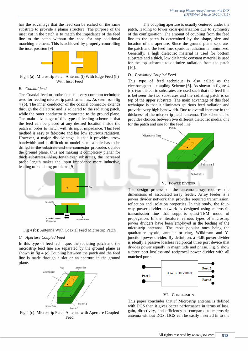
A. Microstrip Line Feed
In this type of feed technique, a conducting strip is
connected directly to the edge of the microstrip patch as
shown in fig 4 (a). The conducting strip is smaller in width
as compared to the patch and this kind of feed arrangement
Micro strip Planar Array Antenna with DGS
(IJSRD/Vol. 2/Issue 09/2014/115)
All rights reserved by www.ijsrd.com 518
has the advantage that the feed can be etched on the same
substrate to provide a planar structure. The purpose of the
inset cut in the patch is to match the impedance of the feed
line to the patch without the need for any additional
matching element. This is achieved by properly controlling
the inset position [9]
Fig 4 (a): Microstrip Patch Antenna (i) With Edge Feed (ii)
With Inset Feed
B. Coaxial feed
The Coaxial feed or probe feed is a very common technique
used for feeding microstrip patch antennas. As seen from fig
4 (b). The inner conductor of the coaxial connector extends
through the dielectric and is soldered to the radiating patch,
while the outer conductor is connected to the ground plane.
The main advantage of this type of feeding scheme is that
the feed can be placed at any desired location inside the
patch in order to match with its input impedance. This feed
method is easy to fabricate and has low spurious radiation.
However, a major disadvantage is that it provides arrow
bandwidth and is difficult to model since a hole has to be
drilled in the substrate and the connector protrudes outside
the ground plane, thus not making it completely planar for
thick substrates. Also, for thicker substrates, the increased
probe length makes the input impedance more inductive,
leading to matching problems [9].
Fig 4 (b): Antenna With Coaxial Feed Microstrip Patch
C. Aperture Coupled Feed
In this type of feed technique, the radiating patch and the
microstrip feed line are separated by the ground plane as
shown in fig 4 (c).Coupling between the patch and the feed
line is made through a slot or an aperture in the ground
plane.
Fig 4 (c): Microstrip Patch Antenna with Aperture Coupled
Feed
The coupling aperture is usually centered under the
patch, leading to lower cross-polarization due to symmetry
of the configuration. The amount of coupling from the feed
line to the patch is determined by the shape, size and
location of the aperture. Since the ground plane separates
the patch and the feed line, spurious radiation is minimized.
Generally, a high dielectric material is used for bottom
substrate and a thick, low dielectric constant material is used
for the top substrate to optimize radiation from the patch
[10].
D. Proximity Coupled Feed
This type of feed technique is also called as the
electromagnetic coupling Scheme [6]. As shown in figure 4
(d), two dielectric substrates are used such that the feed line
is between the two substrates and the radiating patch is on
top of the upper substrate. The main advantage of this feed
technique is that it eliminates spurious feed radiation and
provides very high bandwidth. Due to overall increase in the
thickness of the microstrip patch antenna. This scheme also
provides choices between two different dielectric media, one
for the patch and one for the feed line
V. POWER DIVIDER
The design process of the antenna array requires the
dimensions of associated array feeder. Array feeder is a
power divider network that provides required transmission,
reflection and isolation properties. In this study, the four-
way power divider network is designed using microstrip
transmission line that supports quasi-TEM mode of
propagation. In the literature, various types of microstrip
power dividers have been employed in the feeding of the
microstrip antennas. The most popular ones being the
quadrature hybrid, annular or ring, Wilkinson and Y-
junction power divider. By definition, a -3dB power divider
is ideally a passive lossless reciprocal three port device that
divides power equally in magnitude and phase. Fig. 5 show
a three port lossless and reciprocal power divider with all
matched ports
VI. CONCLUSION
This paper concludes that if Microstrip antenna is defined
with DGS then it gives better performance in terms of loss,
gain, directivity, and efficiency as compared to microstrip
antenna without DGS. DGS can be easily inserted in to the

Micro strip Planar Array Antenna with DGS
(IJSRD/Vol. 2/Issue 09/2014/115)
All rights reserved by www.ijsrd.com 519
antenna which reduces the size and cost of micro strip array
antenna because using multiple arrays can create mutual
coupling between them. To reduce these coupling arrays of
antenna will have to on larger distances which results in
increase of size and cost. To overcome this problem DGS is
introduced because it behaves like a filter effect in between
different arrays of antenna and hence these multiple arrays
can be placed at shorter distance which reduces its size. This
technique can be helpful for various wireless and Mobile
communication systems since the major problem with these
systems are because of radiating and absorbing energy
through antenna. By improving various parameters of
antenna through this DGS technique can help in successful
operations in the network.
REFERENCES
[1] C. A. Balanis, Antenna Theory, 2nd ed., New
York: John Wiley & Sons Inc., (2005).
[2] David M. Pozar, “Microstrip Antennas” Proceeding
of the IEEE. Vol.80, No. 1, January 1992
[3] F. Y. Zulkifli, E. T. Rahardjo, and D. Hartanto,
“Radiation properties enhancement of triangular
patch microstrip antenna array using hexagonal
defected ground structure”, Progress In
Electromagnetics Research M, Vol. 5, pp. 101–109,
2008
[4] D. M. Pozar, Microwave Engineering, 3rd ed.
New York: John Wiley &Sons Inc., 2003.
[5] M. Salehi, A. Motevasselian, A. Tavakoli, & T.
Heidari, “Mutual Coupling reduction of Microstrip
antennas using Defected Ground Structure”
Progress in Antenna. Vol. 1-4244-0411-8/06/
[6] A.K. Arya, M. V. Kartikeyan, and A. Patnaik,
“Defected ground structure in the perspective of
microstrip antennas: A review,” Frequenz, Int.
Journal of RF- Engg. &Telecomm. Vol. 64, pp. 79-
84, 2010.
[7] Paul Hallbjörner, “The Significance of Radiation
Efficiencies When Using S-Parameters to Calculate
the Received Signal Correlation from Two
Antennas”. Antennas and wireless Propagation.
IEEE Letters, Vol. 4, 2005
[8] Shigeru Egashira and Eisuke Nishiyama, “Stacked
Microstrip Antenna with Wide Bandwidth and
High Gain”. Transactions on antennas and
Propagation, IEEE. Vol. 44, No. 11, Nov.1996
[9] M.A. Matin, A.I.Sayeed, “A Design Rule for Inset-
Fed Rectangular Microstrip Patch Antenna”,
WSEAS Transactions on Comm., Volume 9,
January 2010.
[10] B. Kasi and C. K. Chakrabarty, “Ultra wideband
antenna array design for target detection”, Progress
In Electromagnetic Research C, Vol. 25, pp. 67-79,
2012.
[11] E. Levine, G. Malamud, S. Shtrikman,, D Travis,
“A Study of Microstrip Array Antennas with the
Feed Network”. Transactions of antenna and
Propagation, IEEE. Vol. 37, No. 4, April.1989.
[12] TianyuJia, Hua Zhu and Xiuping Li, “A minimized
wideband antenna array with decoupling networks
for UHF RFID applications” ,Progress In EM
Research C, Vol. 35, pp. 237-252, 2013.