micro-mechanical voltage tunable fabry- perot filters ...mln/ltrs-pdfs/nasa-97-tp3702.pdf ·...
TRANSCRIPT
September 1997
NASA Technical Paper 3702
Micro-Mechanical Voltage Tunable Fabry-Perot Filters Formed in (111) Silicon
James D. Patterson
National Aeronautics andSpace Administration
Langley Research CenterHampton, Virginia 23681-2199
September 1997
NASA Technical Paper 3702
Micro-Mechanical Voltage Tunable Fabry-Perot Filters Formed in (111) Silicon
James D. PattersonLangley Research Center, Hampton, Virginia
Available from the following:
NASA Center for AeroSpace Information (CASI) National Technical Information Service (NTIS)800 Elkridge Landing Road 5285 Port Royal RoadLinthicum Heights, MD 21090-2934 Springfield, VA 22161-2171(301) 621-0390 (703) 487-4650
The information in this report was offered as a thesis in partialfulfillment of the requirements for the Degree of Doctor ofPhilosophy in Electrical Engineering, University of Colorado,Boulder, Colorado.
iii
Abstract
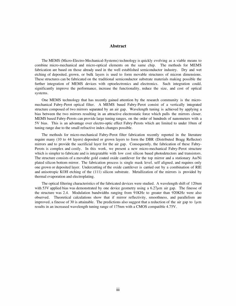
The MEMS (Micro-Electro-Mechanical-Systems) technology is quickly evolving as a viable means tocombine micro-mechanical and micro-optical elements on the same chip. The methods for MEMSfabrication are based on those already used in the well established semiconductor industry. Dry and wetetching of deposited, grown, or bulk layers is used to form movable structures of micron dimensions.These structures can be fabricated on the traditional semiconductor substrate materials making possible thefurther integration of MEMS devices with optoelectronics and electronics. Such integration could,significantly improve the performance, increase the functionality, reduce the size, and cost of opticalsystems.
One MEMS technology that has recently gained attention by the research community is the micro-mechanical Fabry-Perot optical filter. A MEMS based Fabry-Perot consist of a vertically integratedstructure composed of two mirrors separated by an air gap. Wavelength tuning is achieved by applying abias between the two mirrors resulting in an attractive electrostatic force which pulls the mirrors closer.MEMS based Fabry-Perots can provide large tuning ranges, on the order of hundreds of nanometers with a5V bias. This is an advantage over electro-optic effect Fabry-Perots which are limited to under 10nm oftuning range due to the small refractive index changes possible.
The methods for micro-mechanical Fabry-Perot filter fabrication recently reported in the literaturerequire many (10 to 44 layers) deposited or grown layers to form the DBR (Distributed Bragg Reflector)mirrors and to provide the sacrificial layer for the air gap. Consequently, the fabrication of these Fabry-Perots is complex and costly. In this work, we present a new micro-mechanical Fabry-Perot structurewhich is simpler to fabricate and is integratable with low cost silicon based photodetectors and transistors.The structure consists of a movable gold coated oxide cantilever for the top mirror and a stationary Au/Niplated silicon bottom mirror. The fabrication process is single mask level, self aligned, and requires onlyone grown or deposited layer. Undercutting of the oxide cantilever is carried out by a combination of RIEand anisotropic KOH etching of the (111) silicon substrate. Metallization of the mirrors is provided bythermal evaporation and electroplating.
The optical filtering characteristics of the fabricated devices were studied. A wavelength shift of 120nmwith 53V applied bias was demonstrated by one device geometry using a 6.27µm air gap. The finesse ofthe structure was 2.4. Modulation bandwidths ranging from 91KHz to greater than 920KHz were alsoobserved. Theoretical calculations show that if mirror reflectivity, smoothness, and parallelism areimproved, a finesse of 30 is attainable. The predictions also suggest that a reduction of the air gap to 1µmresults in an increased wavelength tuning range of 175nm with a CMOS compatible 4.75V.
iv
Acknowledgments
I am indebted to many individuals who have assisted me during the study of the micro-mechanicalfilters. I would like to thank and acknowledge them for their efforts.
My advisor, Professor Bart Van Zeghbroeck has provided countless hours of discussion and advice thathave propelled the research along the way. I am indebted to him for this and also for his strong optimismthat kept me going during times of frustration.
I would like to thank the Ph.D. committee members for their input into the research, especially theirguidance on the critical issues, that formed the framework of the research.
I am extremely grateful to Professor Bill May for many hours of discussion on the processing issuesand his many hours of assistance in the integrated circuit lab. I also thank Skip Wichart for his advice andthe many times in which he repaired the reactive ion etcher.
Special thanks is owed to the Optoelectronics Division at the National Institute of Standards andTechnology (NIST) at Boulder for the use of their Ti:Sapphire laser system in the spectral analysis of theFabry-Perot filters. Specific thanks is owed to Kevin Knopp for setting up and trouble shooting thespectral analysis system and to Dave Christensen who offered NIST's services for this study.
v
Contents
Abstract............................................................................................................................iii
Acknowledgements ............................................................................................................. iv
List of Tables ...................................................................................................................vii
List of Figures................................................................................................................. viii
I. Introduction................................................................................................................1
1.1 MEMS: an Overview...........................................................................................11.2 MEMS based Fabry-Perots: the State of the Art .......................................................11.3 Potential Applications of the Cantilever Fabry-Perot..................................................21.4 A Novel Silicon Based Micro-Mechanical Fabry-Perot................................................31.5 References..........................................................................................................5
II. Electro-Mechanical and Optical Theory............................................................................7
2.1 Introduction........................................................................................................72.2 Electro-Mechanical Theory....................................................................................7
2.2.1 Derivation of the Cantilever Bending Equation ...............................................72.2.2 Derivation of the Cantilever's Frequency Response ....................................... 102.2.3 Numerical Results For the Cantilever Bending and Frequency
Response............................................................................................... 152.3 Optical Theory.................................................................................................. 20
2.3.1 Introduction............................................................................................ 202.3.2 The Calculation of the Transmission and Reflectance Spectra
Using the Matrix Method.......................................................................... 212.4 Numerical Predictions For the Optical Filter: Electro-Mechanical and
Optical Theory Combined................................................................................... 242.5 References........................................................................................................ 31
III. Fabrication of Micro-Mechanical Fabry Perot Filters........................................................ 33
3.0 Introduction...................................................................................................... 333.1 Popular Methods of Micro-Mechanical Fabry-Perot Fabrication Using
Deposited Materials ........................................................................................... 333.2 Anisotropic Etching of Silicon in Potassium Hydroxide ........................................... 333.3 Fabrication of the Fabry-Perots in (111) Silicon: an Overview.................................. 363.4 Fabrication of Fabry Perots Filters in (111) Silicon: Details and Results ..................... 38
3.4.0 Process Objectives................................................................................... 383.4.1 Si Wafer Specifications ............................................................................ 383.4.2 Thermal Oxidation................................................................................... 393.4.3 Masking Materials For Reactive Ion Etching ................................................ 393.4.4 The Photolithographic Mask Design........................................................... 39
3.4.4.1 Mask Design Introduction............................................................. 393.4.4.2 Why Cantilever Mirrors? .............................................................. 403.4.4.3 Mask Design For Electrical Isolation .............................................. 41
vi
3.4.5 Reactive Ion Etching of the Si Well and Isolation Trench................................ 413.4.6 KOH Undercutting of the Silicon Dioxide .................................................... 43
3.4.6 .1 Lower Than Expected KOH Selectivities.......................................... 443.4.7 Chip Rinsing and Nitric Acid Treatment ...................................................... 503.4.8 Metal Electroplating of the Lower Mirror..................................................... 503.4.9 Drying of the Cantilever Structures Following Wet Processing........................ 53
3.4.9.1 Drying Through Room Air Evaporation and thePinning/Sticking Problem ............................................................ 53
3.4.9.2 Critical Point Drying................................................................... 563.4.10 Top Mirror Metal Evaporation ................................................................... 573.4.11 Stress Induced Cantilever Mirror Curvature................................................... 59
3.5 References........................................................................................................ 60
IV. Electro-Mechanical and Electro-Optical Characterization.................................................... 63
4.1 Introduction...................................................................................................... 634.2 SEM Characterization of the Electro-Mechanical Behavior......................................... 634.3 Electro-Optical Characterization: Wavelength Resolved............................................ 67
4.3.0 Introduction............................................................................................ 674.3.1 Spectral Analysis of a Modulator Without Ni: Early Spectral
Results.................................................................................................. 684.3.2 Spectral Analysis of a Modulator Including the Ni Layer................................. 70
4.4 Electro-Optical Characterization: Time Resolved .................................................... 804.5 References........................................................................................................ 85
V. Conclusion ............................................................................................................ 87
5.1 Summary of the Study: Major Issues ................................................................... 875.2 Micro-Mechanical Fabry-Perot Performance Comparison .......................................... 885.3 References........................................................................................................ 89Comprehensive List of References................................................................................ 91

vii
List of Tables
Table
2-1. Material Constants Used in the Bending Theory and Frequency Response Calculations ... 15
2-2. Optical constants Used in the Theoretical Analysis .................................................. 24
3-1. RIE Etch Rates of Silicon, Silicon Dioxide, and Negative Photoresist in CF4.............. 43
3-2. Measured KOH Etch Rates and Selectivities of Silicon and Silicon Dioxide.................. 46
3-3. KOH Etch Rates and Selectivities Reported by Waggener.......................................... 47
5-1. Micro-Mechanical Fabry-Perot Performance Comparison .......................................... 89
viii
List of Figures
Figure
1-1 An array of micro-mechanical Fabry-Perot filters is used as a WDMdemultiplexer with wavelength tracking capability.............................................3
1-2. Cross-sectional diagram of the novel Si (111) based micro-mechanicalFabry-Perot filter.........................................................................................4
2-1. Cantilever schematic for the electro-mechanical analysis .....................................7
2-2. Diagram used for the calculation of the moment of inertia for thecantilever beam...........................................................................................9
2-3. Cantilever profiles for 2.5 and 5.0 volt bias. The cantilever length is 100 µm andhas a 0 voltage air gap of 1 µm. The oxide thicknesses is 0.85 µm.................... 15
2-4. Cantilever profiles for 15 and 30 volts. The cantilever length is 100 µm and has a 0voltage air gap of 4 µm. ............................................................................. 16
2-5. The position of the cantilever tip as the bias is swept in the forward and reversedirections for a hco = 1 µm air gap cantilever. ................................................ 17
2-6. The position of the cantilever tip as the bias is swept in the forward and reversedirections for a 4 µm air gap cantilever. ......................................................... 18
2-7. Forward and reverse sweep of the bias voltage under the V<Vth constraint forcantilevers with hco equal to 1, 2, and 4µm. .................................................. 18
2-8. Theoretical Bode plot showing the cantilever tip displacement response. The theorymodels the cantilever as a linear-spring point-mass system that is described byEq. 2-13. The oxide cantilever was 101 µm long by 20 µm wide with a thicknessof 0.85 µm. ............................................................................................ 19
2-9. Bandwidth and cantilever tip deflection as a function of cantilever length.............. 20
2-10. Diagram of the multilayered stack used in the spectral analysis........................... 21
2-11A. Transmission spectra for a 1 µm air gap Fabry-Perot at zero bias. The goldthickness is 20 nm. The finesse of the Fabry-Perot is 8.0. .............................. 25
2-11B. Reflection spectra for a 1 µm air gap Fabry-Perot at zero bias. The gold thickness is 20nm. The finesse of the Fabry-Perot is 8.0. ................................................... 25
2-12. Transmission spectra for a 1 µm air gap Fabry-Perot at zero bias. The gold thickness has been increased from 20 nm to 50 nm providing a finesse increasefrom 8 to 30............................................................................................. 27
2-13. Transmittance and finesse as a function of gold thickness. Power throughputand finesse are traded off.............................................................................. 27
2-14. The spectral transmittance of the Fabry-Perot as a function of tuning voltage.The 0 volt bias air gap is 1 µm and the gold mirror thickness is 40 nm. .............. 28
2-15. Transmission peak wavelength versus tuning voltage for the 1 µm air gapcantilever. ................................................................................................ 28
2-16. Transmission spectrum for a 4 µm air gap Fabry-Perot at zero bias..................... 30
2-17. The spectral transmittance of the Fabry-Perot as a function of tuning voltage.The 0 Volt bias air gap is 4 µm and the gold mirror thickness is 40 nm. ............. 30

ix
2-18. Transmission peak wavelength versus tuning voltage for the 4 µm air gapcantilever. ................................................................................................ 31
3-1. Pyramidal structure formed in (100) Si by KOH etching. ....... ........................... 34
3-2. Rectangular trenches formed in (110) Si by KOH etching.................................. 35
3-3. Schematic of (111) Si following vertical drilling using RIE. ............................. 35
3-4. Cross-sectional diagram of (111) silicon drilled vertically with RIE andfollowed with lateral KOH etching................................................................ 36
3-5. Basic movable mirror fabrication process. ...................................................... 37
3-6. Staircase Si profile which results from 4¡ misalignment with the (111)direction. ................................................................................................. 38
3-7. Cross-section of the wafer following oxide growth and masking for reactive ion etching............................................................................................................... 39
3-8. The single mask required for the fabrication of the micro-mechanical Fabry-Perot filters.The mask incorporates a wide variety of cantilever shapes each surrounded by a hexagonalelectrical isolation trench. ........................................................................... 40
3-9. A SEM photograph of an "H" shaped oxide membrane on Si which issagging due to compressive stress................................................................. 40
3-10. The shape of the cantilever silicon well and the hexagonal isolation trench provideelectrical isolation between the cantilevers and the underlying Si and between individualcantilevers on the die.................................................................................. 42
3-11. A cross-sectional diagram of the wafer showing chromium or photoresistcovered regions that are protected during the RIE vertical etching. ....................... 42
3-12. A cross section of the wafer following RIE of the SiO2 and Si layers. This step exposes(110) facets for subsequent lateral undercutting of the oxide layer duringthe KOH etch step..................................................................................... 43
3-13. Lateral undercutting of the cantilever by rapid wet KOH etching in the (110)direction. ................................................................................................. 44
3-14. The lateral undercutting has completely removed the Si underneath thecantilever. ................................................................................................ 44
3-15A-D. Optical micrographs showing the evolution of the KOH undercutting as a function of etch time. The cantilever is 20 µm wide and is parallel tothe (110) flat. ....................................................................................... 45
3-16. A SEM photo of the entire Fabry-Perot structure including the hexagonalisolation trench following 45 minutes of KOH etching. The KOH etchingof the hexagonal isolation trench has provided uniformly undercut oxideeaves around the inside perimeter of the trench. ............................................... 45
3-17. A graphical comparison between our measured (110)/(111) selectivities and tothose reported by Waggener . The KOH percentage of the etchant is 45%. ........... 48
3-18. A graphical comparison between our measured (110)//SiO2 selectivities andthose reported by Waggener. The KOH percentage of the etchant is 45%............. 48
3-19. The misalignment of the wafer surface normal with the (111) direction resultsin a much higher apparent (111) etch rate due to the (110) etch rate projection....... 49
x
3-20. A Dektak profile underneath a 20 µm wide cantilever. The profile is measuredacross the narrow width of the cantilever near the tip. The measured anglebetween the reference and measurement cursors is 0.13¡. .................................. 50
3-21A. A SEM photo of a cantilever Fabry-Perot structure showing KOH etch residueon the silicon (white specks).This device was rinsed with water followedby acetone................................................................................................ 51
3-21B. A SEM photo of a cantilever Fabry-Perot structure showing the absence of theresidue when cleaned with nitric acid. ............................................................ 51
3-22. A SEM photo of the cantilever Fabry-Perot structure showing theabsence of the residue under the cantilever. This device was not cleanedwith nitric acid.......................................................................................... 52
3-23. A cross-sectional diagram of the Fabry-Perot structure following Ni plating.The Ni has plated only the Si and not the SiO2 preserving the electricalisolation between the top and bottom mirrors. ................................................ 54
3-24. An optical micrograph of a Ni plated 3.2 µm cavity Fabry-Perot. ....................... 54
3-25. An optical micrograph of a Ni plated 0.6 µm air gap Fabry-Perot. Note therough Ni plating under the cantilever and oxide eaves. The roughness is a consequence ofpoor plating solution and gas transport in the narrow gap.................................. 54
3-26A-C. The pinning process of a cantilever that is dried through room air evaporation.. . 55
3-27. A SEM photo of an room air dried cantilever that is pinned down to theSi surface due to capillary and Van der Waals forces. ........................................ 56
3-28. A SEM photo of an air dried Fabry-Perot including the surrounding hexagonalisolation trench. Note that the oxide eaves around the trench have beenpulled down into contact with the Si. These contact points will result inthe loss of electrical isolation between the top and bottom mirror metallization..... 56
3-29. A SEM photo of a CPD dried cantilever which is erect in contrast to the air driedstructures. ................................................................................................ 57
3-30. A SEM photo of a CPD dried cantilever Fabry-Perot which is erect. Note alsothat the oxide eaves used for the electrical isolation are not in contact withsilicon layer below in contrast to the air dried devices. ...................................... 58
3-31. A cross-sectional diagram of a cantilever Fabry-Perot following the topmirror gold evaporation. Note the electrical discontinuity provided bythe underside of the oxide eaves. ................................................................... 58
3-32. A microphotograph of a completely processed micro-mechanical tunableoptical filter based on a movable cantilever mirror. The top side of thecantilever is coated with gold. The silicon underneath the cantilever isplated with nickel. ..................................................................................... 59
3-33. SEM photographs illustrating the stress induced upward cantilever curvature.Thicker oxide cantilevers curve less............................................................... 60
4-1. A photo of the cantilever modulator studied under bias in the SEM. .................... 63
4-2. A cross-sectional schematic of the cantilever modulator studied in the SEM.......... 64
4-3. A SEM photo of the cantilever modulator without an applied bias. ..................... 64
xi
4-4. A SEM voltage contrast photo showing electrical isolation between the topand bottom mirrors of the contacted Fabry-Perot. The top mirror of thecontacted device is also shown to be electrically isolated from the topmirrors of adjacent structures. ..................................................................... 65
4-5. A SEM photo of the cantilever with 0 volts applied bias. ................................. 66
4-6. A SEM photo of the cantilever with 45 volts applied bias. The cantilever hasbeen moved into contact with the silicon surface. ............................................ 66
4-7. The predicted Displacement-Voltage characteristic for the cantilever structurestudied in the SEM.................................................................................... 67
4-8. The experimental arrangement used to spectrally characterize theFabry-Perot filters. .................................................................................... 68
4-9. The cantilever structure which was spectrally analyzed with the Ti:Sapphire laser.The length of the cantilever is a stiff 30 µm. The bottom mirror is not coatedwith nickel and provides only the 35% reflectivity of the bare silicon. ................. 69
4-10. Fabry-Perot spectra taken at 0, 30, and 40 volts. ............................................. 69
4-11. A cross-sectional diagram of a cantilever modulator with a nickel platedbottom mirror........................................................................................... 70
4-12. The Fabry-Perot spectra taken at 40, 44, and 48 volts applied bias. .................... 71
4-13. A comparison between measured and theoretically predicted spectra for the Fabry-Perot at40 volts applied bias. The calculated spectrum assumes ideal, flatand parallel, top and bottom mirrors. ............................................................ 72
4-14. Mirror profiles of the Fabry-Perot. The 101 µm long cantilever is curvingupwards due to stress damage. The bottom mirror is angled at -0.5¡ torepresent the worst case staircase effect. The bias between the two mirrorsis 40 volts. .............................................................................................. 73
4-15. The measured intensity profile of the focused light beam on the top mirror.The profile is fitted with a s = 5 µm gaussian function. The gaussianfunction is used to weight the spectra in the summation. .................................. 74
4-16. Reflectance as a function of wavelength for various spot sizes. Here the spectralsummation approximation was used to calculate the total reflectance. The mirror profilesare those from Figure 4-14. ......................................................................... 75
4-17. Experimental and theoretical spectra for the 101 µm long cantilever. The non Ideal Fabry Perot theoretical spectrum was calculated using the summation approximation............................................................................................................... 76
4-18. Experimental and theoretical spectra for the 101 µm long cantilever. Thetheoretical spectra were calculated using the weighted spectral summation.The dashed curves represent the theoretical spectra for the case of, bothstress induced curvature of the top mirror and an angled bottom mirror,and only including curvature of the top mirror. The degradation due tothe top mirror curvature is dominant. ............................................................ 77
4-19. The minimum reflectance wavelength for one cavity mode as a function of applied DCvoltage. The theoretical predictions using 5.0 X 10¹⁰ N/m2 for the oxide elasticitymodulus closely match the experimentally measured values. .............................. 78
4-20. On/Off ratio versus voltage for the cantilever Fabry-Perot. ................................ 79
xii
4-21. Repeatability of the cantilever Fabry-Perot spectra before and after cycling thecantilever from 0 to 54 volts and back ten times. Both spectra were measuredat 40 V applied bias. Significant changes in the spectrum were not observed........ 79
4-22. Spectrum repeatability before and after 8 hours of oscillation at a 10 Khz drive frequency.The applied voltage consisted of a 41 V DC bias in series witha 5 V peak-to-peak sinusoidal signal. ........................................................... 80
4-23. An illustration of the biasing scheme used for the time resolved measurements. ... 81
4-24. Modulation of 830 nm laser light by a cantilever modulator driven at 10 KHz.The DC bias was 21 V. .............................................................................. 82
4-25. Modulation of 830 nm laser light by a cantilever modulator driven at itsresonance frequency of 57 KHz. Note the higher order frequencycomponents in the photodetector signal due to the large cantilever deflection. ....... 82
4-26. Frequency response of a cantilever modulator with length 101 µm...................... 83
4-27. Frequency response of a cantilever modulator with of length 45 µm. ................... 83
4-28. Bandwidth and resonant frequency versus cantilever length. The calculatedvalues are shown by the lines and the experimental values by the diamonds.The elasticity modulus used in the theoretical curves was 5.0 X 10¹⁰ N/m2. ....... 84
4-29. Bandwidth and resonant frequency versus cantilever length. The calculatedvalues are shown by the lines and the experimental values by the diamonds.The elasticity modulus used in the theoretical curves was 7.3 X 10¹⁰ N/m2. ....... 85
1
I. Introduction
1.1 Micro-Electro-Mechanical-Systems (MEMS): an Overview
The MEMS technology is quickly evolving as a viable means to combine micro-mechanical, micro-optical, opto-electronic, and electronic devices on the same chip. The methods for MEMS fabrication arebased on those already used in the well established semiconductor industry. Dry and wet etching of depos-ited, grown, or bulk layers is used to form moveable micron sized structures. These micro-mechanicalstructures can be formed on traditional semiconductor substrate materials including silicon and galliumarsenide. This makes possible the integration of micro-mechanical systems with transistors, optical trans-mitters, and photodetectors. The monolithic realization of these electro-optical systems will provide manyadvantages including higher performance, lower cost, and reduced size.
Historically, micro-mechanics had its beginnings during the early years of the integrated circuit indus-try. In 1965 H. C. Nathanson et al. of Westinghouse Research Laboratories invented the silicon basedresonant gate transistor [1, 2]. The transistor used a cantilever based gate electrode to control the channeltransconductance. The strong mechanical resonance of the cantilever provided a high-Q bandpass electricalfilter. Nathanson's work generated a brief flurry of interest in micro-mechanics. However, the interestwaned, due to the ease in which the filtering behavior could be implemented electronically. Slowly, micro-mechanics has evolved with emphasis on applications that could not be implemented with the same per-formance and simplicity using electronics. For many years following, the fabrication of ink jet nozzles andprint heads represented the main thrust in micro-mechanics [3Ð5].
Today, the MEMS technology has widespread applications in many areas. These areas include micro-optics, mechanical actuation, and sensing. Tiny optical benches on a chip are now possible. TexasInstruments has developed and is currently marketing arrays of digital micro-mirror devices for use in over-head projectors and printers [6]. In the area of optical communications MEMS based Fabry-Perot opticalfilters are being used to tune to and track WDM (Wavelength Division Multiplexing) signals[7Ð14]. Acceleration, pressure, and temperature sensors based on micro-mechanics are being developed andare available off-the-shelf [15Ð17]. These and growing numbers of applications are being developed to takeadvantage of the integrateability of optics, electronics, and micro-mechanics on a single substrate.
1.2 MEMS Based Fabry-Perot Filters: The State of the Art
One MEMS device that has recently (in the past few years) gained increased attention is the tunablemicro-mechanical Fabry-Perot filter. These micro-mechanical Fabry-Perot filters consist of two mirrorsseparated by an air gap. The structure is formed vertically. The mirrors either consist of multilayer DBR(Distributed Bragg Reflector) stacks or a highly reflective metallic layers such as gold. The air gap isformed by the etching of a sacrificial layer. The top mirror is freely suspended above the bottom mirror. Avoltage applied between electrical contacts on the two mirrors results in an attractive electrostatic forcewhich pulls the top mirror down. Consequently, the air gap and transmission wavelength of the Fabry-Perot are reduced.
Traditionally, semiconductor Fabry-Perots have provided tuning based on a cavity refractive indexchange through the Stark and the electro-optic effects. The tuning range of these devices have been limitedto less than 10 nm due to the small index changes possible [8, 18, 19]. On the other hand, micro-mechani-cal Fabry-Perots with tunable air gaps provide much wider tuning ranges than their Stark or electro-opticeffect counterparts. Micro-mechanical Fabry-Perots have demonstrated a tuning range as high as 70Ênmwith a maximum 5 volts applied bias.
Both GaAs and Si based micro-mechanical Fabry-Perots have been investigated and have shown prom-ising performance characteristics. Researchers at Stanford University and the University of California atBerkley have been working with GaAs based micro-mechanical Fabry Perots. The thrust of their work hasdealt with controlling the output wavelength of VCSEL s (Vertical Cavity Surface Emitting Lasers) with atunable coupled cavity micro-mechanical Fabry-Perot [7, 9, 10, 20]. M.S. Wu et al. have fabricated and
2
have tested a GaAs based micro-mechanical Fabry-Perots with the largest tuning range [20]. The Fabry-Perot demonstrated 70 nm of wavelength tuning (wavelength range: 900 to 970 nm) with a maximum of4.9 volts bias. The linewidth of the transmission spectra was less than 10 nm. Their design incorporatestwo molecular beam epitaxy grown AlAs/GaAs Distributed Bragg Reflector (DBR) mirrors separated by anair gap. The top and bottom DBR mirrors use 12.5 and 9 quarter wavelength pairs respectively. The topDBR mirror geometry is a cantilever and moves by a bending motion.
A group at the National Nano Fabrication facility at Cornell is currently fabricating silicon basedmicro-mechanical Fabry-Perots. A. T. T. D. Tran et al. have fabricated a silicon based Fabry-Perot whichuses two three and a half period CVD (Chemical Vapor Deposition) deposited Si/SiO2 DBR mirrors for thecavity [11Ð13]. Tran achieved 40 to 60 nm (wavelength range: 1490 to 1540 nm) of tuning with 65 voltsmaximum bias applied to the structure. A 5 nm linewidth was typical for this device. The top suspendedmirror for this structure was held on four sides, and consequently moved by more difficult stretching insteadof bending like the GaAs cantilevers.
As mentioned previously, the air gap micro-mechanical Fabry-Perot filters provide a larger tuning rangethan their Stark effect counterparts. However, there are disadvantages and problems associated with themicro-mechanical Fabry-Perots. Although they provide a large tuning range there is a tradeoff in band-width. Practical Fabry-Perots have demonstrated bandwidths of less than 1Mhz [1, 2, 21]. Yields of thedevices have been less than desirable. The suspended mirrors are fragile and require careful handling follow-ing air gap formation. Due to their fragility, integration with electronics requires that the Fabry-Perot airgap formation be the last step. Stress due to differences in the thermal coefficients of expansion havecaused the Fabry-Perot mirrors to curve resulting in a less than stable optical resonator [13]. Lifetimes ofthe movable mirrors are sometimes limited to fatigue [21]. If wet etching is used to remove the sacrificiallayer, capillary and intersolid forces during the rinse/dry step could result in plastic deformation of the struc-ture and the potential pinning of the two mirrors together [22].
1.3 Potential Applications of the Cantilever Micro-Mechanical Fabry-Perot
There are many applications in which the modulator can be used. Here we present a few potential pos-sibilities although there may be many others.
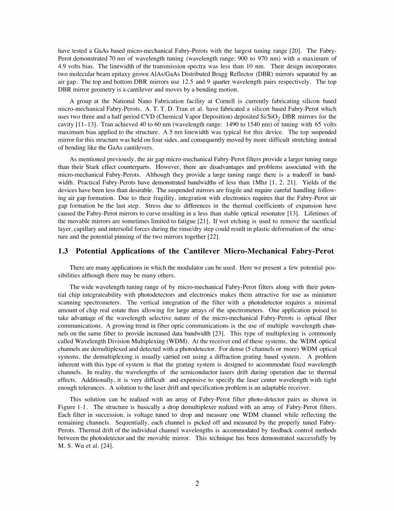
The wide wavelength tuning range of by micro-mechanical Fabry-Perot filters along with their poten-tial chip integrateability with photodetectors and electronics makes them attractive for use as miniaturescanning spectrometers. The vertical integration of the filter with a photodetector requires a minimalamount of chip real estate thus allowing for large arrays of the spectrometers. One application poised totake advantage of the wavelength selective nature of the micro-mechanical Fabry-Perots is optical fibercommunications. A growing trend in fiber optic communications is the use of multiple wavelength chan-nels on the same fiber to provide increased data bandwidth [23]. This type of multiplexing is commonlycalled Wavelength Division Multiplexing (WDM). At the receiver end of these systems, the WDM opticalchannels are demultiplexed and detected with a photodetector. For dense (5 channels or more) WDM opticalsystems, the demultiplexing is usually carried out using a diffraction grating based system. A probleminherent with this type of system is that the grating system is designed to accommodate fixed wavelengthchannels. In reality, the wavelengths of the semiconductor lasers drift during operation due to thermaleffects. Additionally, it is very difficult and expensive to specify the laser center wavelength with tightenough tolerances. A solution to the laser drift and specification problem is an adaptable receiver.
This solution can be realized with an array of Fabry-Perot filter photo-detector pairs as shown inFigureÊ1-1. The structure is basically a drop demultiplexer realized with an array of Fabry-Perot filters.Each filter in succession, is voltage tuned to drop and measure one WDM channel while reflecting theremaining channels. Sequentially, each channel is picked off and measured by the properly tuned Fabry-Perots. Thermal drift of the individual channel wavelengths is accommodated by feedback control methodsbetween the photodetector and the movable mirror. This technique has been demonstrated successfully byM. S. Wu et al. [24].
3
Movable Mirrors
V1 V2 V3
+
-
+
-
+
-
Fixed Mirror
Integrated Mirrorand Photodetector
Transmitted And Detected Wavelengths
WDM Input
Si or GaAs Substrate
Red Green Blue
Figure 1-1. An array of micro-mechanical Fabry-Perot filters is used as a WDM demultiplexer withwavelength tracking capability.
Another possible application for the tunable filters is a flat panel display using the Fabry-Perot as a colorproducing pixel element. Black and white displays have been demonstrated using thick metal-coated mov-able cantilever mirrors by IBM researchers in 1977 [25]. The imaging system used a quasi-collimated lightsource to illuminate arrays of the cantilever mirrors. The display image was formed by directing the lightfrom each cantilever mirror in or out of the numerical aperture of the imaging lens. This imaging systemwas probably the precursor to Texas Instruments' Digital Micro-Mirror Device (DMD) display[6].
Optically interrogatable acceleration and temperature sensing are also possibilities for the micro-mechanical Fabry-Perot filter. Cantilever bending due to acceleration forces can be translated into the spec-tral transmission shift of a broadband source or the power modulation of monochromatic laser light.Temperature sensing is possible by the fabrication of the movable mirror with two materials with largedifferences in thermal coefficient of expansion. This large difference can be used to produce the bimetallicbending effect. The thermal stress induced bending of the movable mirror results in an optical cavity lengthchange. The temperature dependent cavity length is used to relate temperature to the spectral transmissionproperties of the Fabry-Perot.
1.4 A Novel Silicon Based Micro-Mechanical Fabry-Perot
The fabrication of the micro-mechanical Fabry-Perots as reported in the literature rely on multilayereddeposited films for the mirrors and selective isotropic removal of a deposited sacrificial layer to form the airgap. Consequently, the fabrication of these micro-mechanical Fabry-Perots is time consuming, requiresexpensive and complicated film growth equipment (especially MBE), and is potentially costly.
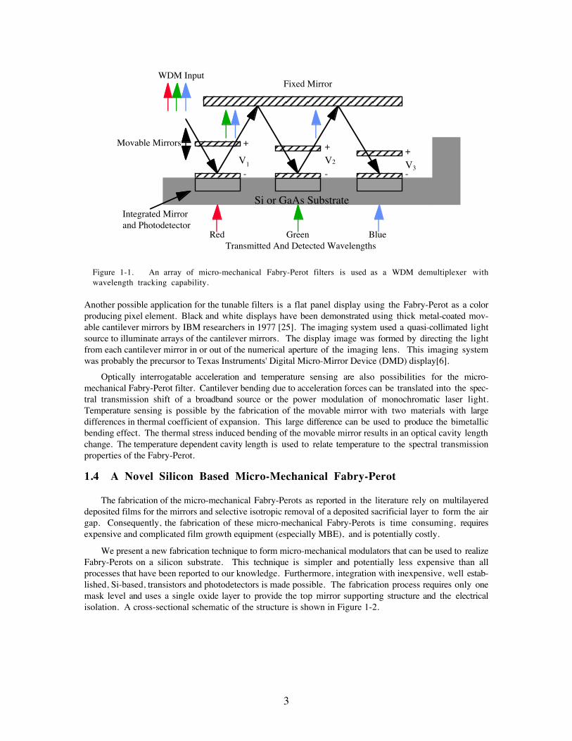
We present a new fabrication technique to form micro-mechanical modulators that can be used to realizeFabry-Perots on a silicon substrate. This technique is simpler and potentially less expensive than allprocesses that have been reported to our knowledge. Furthermore, integration with inexpensive, well estab-lished, Si-based, transistors and photodetectors is made possible. The fabrication process requires only onemask level and uses a single oxide layer to provide the top mirror supporting structure and the electricalisolation. A cross-sectional schematic of the structure is shown in Figure 1-2.
4
Si (111)
Gold
Ni/Gold
Air Gap
SiO2
Figure 1-2. Cross-sectional diagram of the novel (111) silicon based micro-mechanical Fabry-Perot filter.
A (111) oriented silicon substrate is used. The movable top mirror is a cantilever made of high qualitythermally grown SiO2. A cantilever structure was chosen due to the much lower voltages required to bendthe structure in comparison to the stretching of a membrane fixed on two or more ends. The formation ofthe air gap under the cantilever is accomplished by a combination of vertical RIE (Reactive Ion Etching) andlateral anisotropic selective KOH wet etching of the (111) silicon. The substrate itself provides the sacrifi-cial layer. The metallization of the top mirror is carried out by gold evaporation while the bottom mirror iselectroplated with nickel followed by gold.
The structure can function as both a filter and a photodetector in the 700Ð900 nm wavelength range bysimply implanting or diffusing a p-n junction photodetector into the substrate under the bottom mirror.The filter can also operate in unattenuated transmission through the substrate at wavelengths longer than the1100 nm cutoff wavelength of the silicon.
In comparison with the micro-mechanical Fabry-Perot filters currently being developed from the litera-ture, this structure has the advantage of being simpler in construction and fabrication complexity. However,the utilization of simple metallic mirrors results in a performance tradeoff not suffered by Fabry-Perotsusing DBR mirrors. Fabry-Perots using metallic mirrors cannot provide both high finesse and high trans-mittance simultaneously due to optical absorption in the metal. That is, the effective mirror reflectivity isincreased with a thicker metal layer which yields a higher finesse. However, the optical throughput isreduced. In light of this tradeoff, we present the simple structure as an inexpensive alternative to the DBRbased Fabry-Perots for applications where the tradeoff can be tolerated.
We begin in Chapter 2 by presenting a theoretical description of the cantilever bending. The bendingof the cantilever will be related to the physical characteristics of the structure and the applied voltage. Ahysteretic behavior is predicted. However, it is shown to be avoidable if the applied voltages are below athreshold value. The optical filtering behavior of the structure is related to the device geometry and voltage.Numerical results are presented and predict reasonable device performance characteristics and reveal perform-ance tradeoff issues.
In Chapter 3, the modulator fabrication process is described. A new method for cantilever undercuttingusing (111) Si wafers is presented. Mask design methods are presented that provide efficient undercutting ofthe oxide cantilever and the necessary electrical isolation between the mirrors. Details of the mirrormetallization are presented. Top mirror metal evaporation and bottom mirror electroplating are discussed.Structural and processing problems will be revealed that result in the deviation of the mirror surfaces fromperfect smoothness and flatness.
In Chapter 4, the experimental results for the micro-mechanical Fabry-Perots are presented. Resultsfrom a SEM study of the motion of the cantilever under bias and the spectral tuning characteristics of thefilter are also presented. The spectra were measured as a function of applied bias. The spectral characteriza-tion includes tuning voltage versus transmission wavelength, linewidths, and on/off ratios. The frequencyresponse characteristics of the modulator are also presented. The experimental results are compared to theo-retical predictions.
Finally in Chapter 5 we summarize the results and suggest modulator design improvements that could
5
result in better filter performance.
References
1 . Nathanson, H. C. and R. A. Wickstrom, A resonant gate silicon surface transistor with high-Q bandpassproperties. App. Phys. Ltrs., 7, p. 84, 1965.
2 . Nathanson, H. C., et al., A resonant gate transistor, IEEE Trans. on Elect. Dev., ED-14, p. 117, 1967.
3 . Bassous, E., H. H. Taub, and L. Kuhn, Ink jet printing nozzle arrays etched in silicon, App. Phys. Ltrs.,31 , p.Ê135, 1977.
4 . Wolber, W. G. and K. D. Wise, Sensor development in the microcomputer age, IEEE Trans. Elect. Dev.,ED-26 , p. 1864, 1979.
5 . Middelhoek, S., J. B. Angell, and D. J. W. Noorlag, Microprocessors get integrated sensors, IEEESpectrum,. 17(2), p. 42, 1980.
6 . Hornbeck, L .J., Digital Light Processing and MEMS: An Overview in IEEE/LEOS 1996 Summer TopicalMeetings: Optical MEMS And Their Applications, Keystone, CO, pp. 7Ð8, 1996.
7 . Chang-Hasnain, C. J., E. C. Vail, and M. S. Wu, Widely -tunable micro-mechanical vertical cavity lasersand detectors in IEEE/LEOS 1996 Summer Topical Meetings: Optical MEMS and Their Applications.1996. Keystone, CO, pp. 43Ð44.
8 . Choa, F.S., et al., InGaAs/InGaAsP integrated tunable detector grown by chemical beam epitaxy, App.Phys. Ltrs., 63(13), pp. 1836Ð1838, 1993.
9 . Harris Jr., J. S., M. C. Larson, and A. R. Massengale, Coupled -cavity laser diode with micromachinedexternal mirrors in IEEE/LEOS 1996 Summer Topical Meetings: Optical MEMS and Their Applications,Keystone, CO, pp. 31Ð32, 1996.
10. Larson, M .C. and J. S. Harris Jr., Broadly-tunable, narrow linewidth resonant cavity light emitter in 53rdAnnual Device Research Conference, Charlottesville, VA, pp. 130Ð131, 1995.
11. Lo, Y. H., et al., Integrated micro-optical interferometer arrays in IEEE/LEOS 1996 Summer Topical Meet-ings: Optical MEMS and Their Applications, Keystone, CO, pp. 25Ð26, 1996.
12. Tran, A. T. T. D., et al., Electro-mechanically tunable micro Fabry-Perot filter array in 53rd Annual DeviceResearch Conference, Charlottesville, VA, pp. 128Ð129, 1995.
13. Tran, A. T. T. D., et al., Surface Micromachined Fabry-Perot Tunable Filter. Photonics TechnologyLetters, 8(3), pp. 393Ð395, 1996.
14. Uenishi, Y., Coupled-cavity laser diode with micromachined external mirrors in IEEE/LEOS 1996 SummerTopical Meetings: Optical MEMS and Their Applications, Keystone CO, pp. 33Ð34, 1996.
15. Fricke, J. and E. Obermeier, Surface Micromachined Accelerometer Based On A Torsional Moving Structurein The 8th International Conference on Solid-State Sensors and Actuators, Stockholm, Sweden, pp. Ê542Ð545, 1995.
16. Goldman, K. and M. Mehregany, A Novel Micromechanical Temperature Memory Sensor in The 8thInternational Conference on Solid-State Sensors and Actuators, Stockholm, Sweden, pp. 132Ð135, 1995.
17. Neikirk, Y. K. A. D. P., Monolithically integrated optically interrogated pressure microsensor, AcousticSoc. America, p. 2353, 1992.
18. Wipiejewski, T., et al., Tunable extremely low threshold vertical cavity laser diodes, IEEE PhotonicsLtrs., 5(8), pp. 889Ð892, 1993.
19. Martinet, E., et al., Electrical tunability of infrared detectors using compositionally asymmetricGaAs/AlGaAs multiquantum wells, App. Phys. Ltrs.,. 60(7), pp. 895Ð897, 1992.
20. Wu, M. S., et al. Widely tunable micromachined gallium arsenide fabry-perot filters in IEEE/LEOS,Keystone CO, 1994.
21. Petersen, K. E., Silicon as a mechanical material, Proceedings of the IEEE, 70(5), pp. 420Ð457, 1982.
6
22. Mastrangelo, C. H. and C. H. Hsu, Mechanical Stability and Adhesion of Microstructures: Part I: BasicTheory. Journal of Micro-mechanical Systems, 2(1), pp. 33Ð43, 1993.
23. Brackett, C. A., Dense wavelength division multiplexing networks: Principles and applications, IEEEJournal of Selected Areas in Communications, 8(6), pp. 948Ð964, 1990.
24. Wu, M. S., et al., Widely and continuously tunable micromachined resonant cavity detector withwavelength tracking, IEEE Photonics Tech. Ltrs., 8(1), pp. 98Ð100, 1996.
25. Petersen, K. E., Micromechanical light modulator array fabricated on silicon, App. Phys. Ltrs., 31(8), pp.521Ð523, 1977.
7
II. Electro-Mechanical and Optical Theory
2.1 Introduction
In this chapter, the theory describing the behavior of the voltage tunable Fabry-Perot filters isdeveloped and presented. The analysis is performed in two steps. First, the electro-mechanical behavior ofthe cantilever structure is analyzed. In this section, the voltage induced bending of the cantilever iscalculated. The bending theory is used to relate the applied voltage to the size of the air gap under thecantilever mirror. The second part of the analysis is the calculation of the optical spectra transmitted andreflected by the Fabry-Perot. Given the Fabry-Perot geometry and functional dependence of the air gap onvoltage, the optical filtering characteristics are calculated. In section 2.4 numerical results are presented forseveral cases. The numerical results provide an understanding of how the tuning behavior is affected by theapplied voltage and geometry of the structure, and what the tradeoff issues are. In Chapter 4, the theorypresented in this chapter will be compared to the experimental results.
2.2 Electro-Mechanical Theory
2.2.1 Derivation of the Cantilever Bending Equation
The bending of the cantilever as a function of voltage is described in this section. Figure 2-1 shows aschematic of the cantilever structure described in the analysis with relevant symbol definitions. Thecantilever structure is assumed to be of constant cross-section. However, the theory is amenable to morecomplicated geometries. It is also assumed that ideally the cantilever is straight and parallel to the lowermirror with zero bias applied to the structure.
The structure consists of a gold coated cantilever suspended above a gold coated silicon substrate. Thecantilever forms the top mirror for the Fabry-Perot while the gold coated Si below provides the bottommirror. The length of the cantilever is L. It has a width W, and oxide thickness hox. The height of thecantilever above the bottom mirror with zero bias V is hco. y is defined as the height of the cantileverabove the bottom mirror. With an applied bias y is a function of the lateral position x.
As mentioned in Chapter 1 the basis for the cantilever bending is a capacitive electrostatic force. Wecan treat the cantilever structure as a capacitor since the SiO2 electrically insulates the top mirror metalfrom the Si based mirror below. When a voltage is applied between the cantilever metal and the metal on
SiO2
Si (111)
L
Gold
W
hox
y
xhco
Gold
V
Figure 2-1. Cantilever schematic for the electro-mechanical analysis.
8
the silicon, opposite charges build up on the capacitor plates producing an attractive electrostatic force thatpulls the cantilever toward the silicon.
The force between the cantilever and the Si due to the voltage V can be derived from the equation ofstored energy in a capacitor C.
U CV=1
22 (2-1)
The force F(y), can be obtained by differentiating the stored energy U with respect to the capacitor spacingy. The differentiation is performed while holding the capacitor voltage constant. That is, the voltage isprovided by an ideal source. Differentiating gives
F ydU
dyV
dC
dy( ) = =
1
22
(2-2)
Here the capacitance is the series combination of the cantilever oxide capacitor and the air gap capacitorbetween the bottom of the cantilever and the metal coated Si below.
1 1 1
C C Cox air gap= +
- ,
CC C
C Cox air gap
ox air gap=
+-
- , CWL
hoxo rox
ox=
e e , CWL
yair gapo
- =e (2-3)
e
eo
rox
free space permittivity
SiO relative permittivity
®
® 2
Differentiating the series capacitance combination and substituting into the force equation gives
F ydU
dyV
WL
yh
o
ox
rox
( ) = = -
+é
ëê
ù
ûú
1
22
2e
e (2-4)
The force is shown to be proportional to the square of the ratio of the voltage to the air gap spacing forsmall hox/erox.
The bending of a cantilever under the influence of an arbitrary loading function is given by thecantilever differential equation [1, 2]. This equation provides the steady state or static profile of thecantilever under a distributed load.
d y
dx
M x
EI
2
2 =( )
(2-5)
The height of the cantilever is given by y and the lateral position is given by x as in Figure 2-1. M(x) isthe total moment at a position x. It is the sum of either the total loading moment or torque to the left of xor too the right of x. E is the elasticity modulus of the cantilever material and is frequently called Young'smodulus. In this case E is the elasticity modulus of the oxide. The elasticity of the composite beam isminimally affected by the addition of the thin gold layer. I is the cross-sectional area moment of inertia ofthe beam (a cross-sectional area defined by hox and the width W) and describes the beams stiffness totorsional bending. Here the moment is taken about the central z axis of the beams cross-section as shownin Figure 2-2.
9
y
z
hox
2
-hox
2
W
2
Cantilever Beam Cross-Section
-W
2
Figure 2-2. Diagram used for the calculation of the moment of inertia of the cantilever beam.
For the constant cross-section cantilever shown in Figure 2-1, I is given by
I y dy dzWh
zW
W
yh
yh
ox
ox
ox
= ==-=-
=
òò 2
2
2
2
2 3
12(2-6)
M(x) can be related to the electrostatic force
M xF y x
Lx x dx W
V x x
y xh
dxx x
L
o
ox
rox
x x
L( ) =
( )( )¢ -( )ò ¢ = -
¢ -( )
¢( ) +é
ëê
ù
ûú
ò ¢¢= ¢=
e
e
2
22
(2-7)
The resultant cantilever differential equation is given by
d y
dx EhV
x x
y xh
o
ox ox
rox
x x
L2
2 326
= -¢ -( )
¢( ) +é
ëê
ù
ûú
ò¢=
e
e
(2-8)
One immediately observes that the beam bending under the influence of the electrostatic force does notdepend on the width W of the structure, since it has dropped out of the expression. This is a consequence ofboth the stiffness of the beam and the electrostatic force depending linearly on W. It will also be shownthat the width does not affect the frequency response either. The classification of the equation is a secondorder nonlinear differential equation. It cannot be solved exactly for an analytic solution. Instead, it must besolved using numerical methods.
The numerical solution solves the differential equation by using trapezoidal integration and iteration toprovide convergence of the y input values to y output values. That is, first assume that y(x) isapproximated by hco, the zero voltage air gap. Next, the moment is integrated providing y''(x). Integratey''(x) twice to provide y(x). The values for y(x) are plugged into the moment generating equation again.The iteration is performed until the y(x) solution does not change greater than 1 part in a billion. Themoment integral provides a pulling down of the guessed input values toward the real solution.
10
Convergence occurs, since the first guess for the y values hco is larger than the real solution .
An analytical solution would provide some needed insight to the cantilever's bending sensitivity tovoltage as a function of the structures geometry. If one assumes in the differential equation, that the heighty(x) does not vary significantly from the initial air gap hco (with 0 Volts), y(x) in the denominator of theintegral can be replaced by the constant hco without great loss of accuracy. The replacement provides ananalytical solution which is valid for small V/hco ratios. The small voltage or quadratic approximation is
y x hEh
V
hh
L x Lx xco
o
oxco
ox
rox
( ) = -
+é
ëê
ù
ûú
- +é
ëêê
ù
ûúú
6
4 6 243
2
2
2 2 3 4e
e
(2-9)
The maximum deflection of the cantilever beam occurs at its tip. The position of the tip is given by
y L hEh
V
hh
Lcoo
oxco
ox
rox
( ) = -
+é
ëê
ù
ûú
3
4 3
2
24e
e (2-10)
As shown, the maximum displacement of the beam is proportional to the fourth power of the length. Thedependence of the bending to hox is inverse to the 5th power for small initial cavity height hco. Also, forlarge hco /hox, the displacement goes as the square of the ratio of the voltage to the initial cavity height.
2.2.2 Derivation of the Cantilever's Frequency Response
Another crucial performance metric for the micro-mechanical Fabry-Perot is its deflection response as afunction of the frequency of the applied voltage. From this characteristic we also gain knowledge of thestructures modulation bandwidth which can be used for comparison. Here we present a theoretical methodfor calculating the dependence of the response characteristic and bandwidth on the device geometry. Incalculating the response characteristic, a combination of rigorous and first order theory is used. Acompletely rigorous analysis would require extensive numerical calculations for solutions of transcendentalfunctions. It will be shown in Chapter 4 that the approximate theory predicts a response function that isvery consistent with the experimental data. First the natural resonant frequencies of a freely vibratingcantilever are calculated. The model rigorously describes the distributed mass and elasticity of thecantilever. Next a response function to a sinusoidal driving force is formulated based on a linear-springpoint-mass system. The response function also includes a damping term due to air resistance. Theresponse function includes only the affects of the 1st natural frequency of the cantilever. The naturalfrequency in the first order response function is then replaced by the fundamental or 1st natural frequencycalculated using the rigorous theory. This function provides a prediction for the response characteristic ofthe cantilever and its -3 dB bandwidth. Justification of this model can be obtained from the experimentalresults. Like the frequency response calculated with the linear-spring point-mass model, the measuredresponse for the cantilevers is low pass. Furthermore, the measured response only shows a significantcontribution from the 1st natural frequency. The strength of the higher order natural frequencies arerelatively small probably due to the viscous air damping of the cantilever.
In general, to calculate exactly the analytic solution to the motion of a freely vibrating cantilever oneuses the partial differential equation of motion for the lateral vibration of a beam [3]
¶r
2
2
2
2
2
2xEI
y
xWh
y
teff ox
æ
èç
ö
ø÷ = - .
(2-11)
11
r
r
eff
Au
Au
effectivedensityof thebeam
densityof gold layer
h thicknesof gold layer
. ®
®
®
rr r
effSiO ox Au Au
ox
h h
h. =+
2
(2-12)
Here all variable definitions are the same as previously stated except for the addition of the effective density.The effective density includes contributions to the mass of the cantilever from both the thin gold layer (10to 50 nm) and the thicker oxide layer (850 nm). In the calculation of the bending of the cantilever, thecontribution of the gold layer to the stiffness was negligible. This is a consequence of the gold layer beingmuch thinner than the oxide layer and the elasticity constant of gold 7.8 ´ 1010 N/m2 being comparable tothat of SiO2 7.3 ´ 1010 N/m2 [4]. However, when calculating the mass of the structure the gold must beincluded for an accurate result. Gold's density is a factor of 7.7 higher than that of oxide, 19.3 g/cm3
versus 2.5Êg/cm3 respectively [4, 5]. Consequently the gold layer's contribution to the mass is significant.The solution to the motion equation is separable and is of the form
y x t X x Cos tn( , ) = ( ) +( )w q (2-13)
At this point a new constant is defined
kw r42
=n eff oxWh
EI.
(2-14)
Here wn is one of the natural frequencies of oscillation for the cantilever beam. Substituting Eqs. 2-13 and2-14 into the vibration equation and dividing by Cos(wnt + q) gives
d X x
dxX x
4
44( )
= ( )k(2-15)
The solution to equation 2-15 is of the form
X A Sin x A Cos x A Sinh x A Cosh x= ( ) + ( ) + ( ) + ( )1 2 3 4k k k k (2-16)
The constants A1, A2, A3, and A4 are found by the supporting conditions on the ends of the cantileverbeam. In finding the solutions to Eq. 2-16 it is more convenient to redefine the constants and write it inthe form
X A Cos x Cosh x B Cos x Cosh x
C Sin x Sinh x D Sin x Sinh x
= ( ) + ( )[ ] + ( ) - ( )[ ]+ ( ) + ( )[ ] + ( ) - ( )[ ]
k k k k
k k k k (2-17)
This form will reduce the number of constants in the final solution. The conditions on the ends of thecantilever are as follows.
The deflection is proportional to X and is zero at the built-in end.
The slope is proportional to X' and is zero at the built-in end.
The moment is proportional to X" and is zero at the free end.
12
The shear is proportional to X''' and is zero at the free end.
The required derivatives are
¢ = - ( ) + ( )[ ] + - ( ) - ( )[ ]+ ( ) + ( )[ ] + ( ) - ( )[ ]
X A Sin x Sinh x B Sin x Sinh x
C Cos x Cosh x D Cos x Cosh x
k k k k k k
k k k k k k (2-18)
¢¢ = - ( ) + ( )[ ] + - ( ) - ( )[ ]+ - ( ) + ( )[ ] + - ( ) - ( )[ ]
X A Cos x Cosh x B Cos x Cosh x
C Sin x Sinh x D Sin x Sinh x
k k k k k k
k k k k k k
2 2
2 2(2-19)
¢¢¢ = ( ) + ( )[ ] + ( ) - ( )[ ]+ - ( ) + ( )[ ] + - ( ) - ( )[ ]X A Sin x Sinh x B Sin x Sinh x
C Cos x Cosh x D Cos x Cosh x
k k k k k k
k k k k k k
3 3
3 3(2-20)
Applying the cantilever end conditions to the equations results in
0 = A (2-21)
0 = C (2-22)
0 = ( ) + ( )[ ] + ( ) + ( )[ ]B Cos L Cosh L D Sin L Sinh Lk k k k (2-23)
0 = ( ) - ( )[ ] - ( ) + ( )[ ]B Sin L Sinh L D Cos L Cosh Lk k k k (2-24)
Here A and C are zero due to the conditions on the built-in end of the cantilever. There are still tworemaining constants which have not been determined B, D, and the spatial frequency k is unknown. Oncethe spatial frequency of a given mode has been determined, one of the unknown constants can be found interms of the other. There is always one undetermined constant, which can be evaluated only if theamplitude of the vibration is known. We will not be concerned with this constant since we are calculatingthe normalized response of the cantilever. Using Eqs. 2-23 and 2-24, expressions relating the spatialfrequency to the ratio of D to B can be derived.
D
B
Cos L Cosh L
Sin L Sinh L
Sin L Sinh L
Cos L Cosh L= -
( ) + ( )( ) + ( )
=( ) - ( )( ) + ( )
k kk k
k kk k (2-25)
Rearranging Eq. 2-25 results in
- = ( ) ( )1 Cos L Cosh Ln nk k (2-26)
Eq. 2-26 provides numerical solutions for the spatial frequency given a cantilever length L. Solutions to theproduct of spatial frequency and the length must be obtained using numerical methods. The first fewsolutions are
13
k
k
k
k
1
2
3
4
1 875
4 694
7 855
10 996
L
L
L
L
=
=
=
=
.
.
.
. (2-27)
Of most significance in calculating the response characteristic of spring-mass system is the fundamentalnatural frequency w1. The response of spring-mass system is basically low pass. The fundamentalfrequency is the first and most dominant pole in the response characteristic. Substituting k1L in Eq 2-27into Eq. 2-14 gives an expression for the fundamental natural frequency.
w pr1 1 22 1 015= =f
E h
Leff
ox.. (2-28)
Equation 2-11 is the differential equation for a freely vibrating cantilever beam oscillating only in itsresonant frequencies. To obtain the response of the beam to a continuous external force the external forcemust be included in Eq 2-12 and the particular solution solved for in addition to the homogeneous equation.The solutions to the particular solution are found numerically and are quite cumbersome to calculate. Foran exact solution to the forced oscillator a finite element mechanics program such as MSC/NASTRANshould be used (MSC/NASTRAN is a registered trademark of MacNeil Schwendler Corporation) [6].However, the rigorously calculated 1st natural frequency can be used to adequately model the forced responseof the cantilever when used in combination with the linear-spring point-mass forced oscillator model. Asstated previously from the knowledge of the experimental results the affect of the higher order resonances onthe response are relatively insignificant in comparison to the 1st natural frequency. Consider the simpleharmonic oscillator differential equation.
md y
dt
dy
dtKy F
y displacement
t time
m point mass
dampingcoefficient
K linear springconstant
F applied force
applied
applied
2
2 + + =
®
®
®
®
®
®
g
g
(2-29)
This equation assumes a point-mass, a linear spring, and damping. In the case of the cantilever structures,the damping is caused by viscous air damping. Next, assume a sinusoidal applied force and sinusoidaldisplacement of the same frequency (this requires the spring to be linear)
F Feappliedj t= Ä w
, y Ye j t= Ä w (2-30)
Here the complex F and Y represent the complex amplitude of the applied force and displacementrespectively. w is the angular frequency. Plugging Eq. 2-30 into Eq. 2-29 and calculating the displacementresponse yields:
14
ÄÄ
YF
m
Km
K
m
=
+ -æ
èç
ö
ø÷ +
æ
èç
ö
ø÷w w
g4 22
2
2
2
122
(2-31)
Next recognize that the natural frequency of a linear-spring point-mass system is given by
w pp1 1212
= =fK
m (2-32)
The natural frequency has been subscripted to be the fundamental or first natural frequency. A linear springhas only one natural frequency. We could obtain a resonance frequency based on the linear-spring point-mass model by taking the derivative of Eq. 2.10 with respect to the force. However, this would result inloss of accuracy since the cantilever is a distributed system. Instead we use the more accurate fundamentalnatural frequency calculated by the rigorous theory. Rewriting Eq. 2-31 and normalizing to the DCresponse yields
ÄY
m
f
f fm
f f
=
+ -æ
èç
ö
ø÷ +
æ
èç
ö
ø÷
=
+( )
-æ
èç
ö
ø÷ +
æ
èç
ö
ø÷
w
w wg
w wg
p
12
4 22
2 12
14
12
12
4 22
2 12
14
12
22
2
(2-33)
To numerically calculate the response all that remains to determine is the damping factor. The dampingresults from the viscosity of the air displaced by the motion of the cantilever. Theoretical calculation of thedamping factor is generally very difficult. Consequently in this analysis, the damping factor will bedetermined from the experimental data. At this point another observation is key. In the undamped case wecalculated the natural frequency, the frequency of maximum displacement amplitude for the cantilever. Inthe case of a damped oscillator the frequency of maximum displacement or resonance frequency is reduced incomparison to the undamped case. The shifted resonance is found by minimizing the denominator of theresponse function of Eq. 2-33. The shifted resonance is
w wg
R Nm
= -22
22 (2-34)
For our structures (from experimental measurements) the shift is very small due to small value of the factorcontaining the damping term relative to the square of the natural frequency. The frequency shift for ourstructures is about 4%. Another useful quantity is the -3 dB frequency. Setting Equation 2-33 equal to one-half gives
fm
fm
f fdB-
= -( )
-æ
èç
ö
ø÷ +
( )-
æ
èç
ö
ø÷ +
3
22
2 12
2
2 122
141
2 22
12 2
2 12g
p
g
p (2-35)
An approximate and simple expression for the -3 dB frequency can be found provided again that the termcontaining the damping factor in Eq. 2-35 is much less that containing the fundamental natural frequency.
f f providedm
fdB- »( )
<<3 1
2
2 123
22,
g
p (2-36)

15
2.2.3 Numerical Results For the Cantilever Bending and Frequency Response
In this section, theoretical numerical results for the cantilever structure shown in Figure 2-1 arepresented. The material constants used in the electro-mechanical calculations are listed in Table 2-1.
Table 2-1. Material Constants Used in the Bending Theory and Frequency Response Calculations.
Parameter Symbol Value References
SiO2 Elasticity Modulus
(Fused Silica/OpticalFiber)
E 7.3 ´ 1010 N/m2 [7]
SiO2 Density(Fused Silica/Optical
Fiber)
rSiO22.5 g/cm3 [7]
SiO2 Relative Permittivity eSiO23.9 [5]
Au Density rAu19.3 g/cm3 [4]
Au Elasticity Modulus 2.5 g/cm3 [4]
Figure 2-3 shows the cantilever air gap, y as a function of lateral position x for a cantilever with initialair gap hco = 1 µm.. The length of the cantilever is 100 µm. Profiles are shown for both 2.5 and 5 voltbias. A bias of 2.5 V provides 68 nm of bending at the tip as indicated by both the numerical and lowvoltage solutions. The angle of the cantilever tip is 0.04¡. An application of 5 V provides 472 nm ofbending at the tip with an angle of 0.27¡. The low voltage solution no longer applies and grosslyunderestimates the tip bending by a factor of 2. Note that the long length of the cantilever ensures that thepitch angle is small for a given displacement. A small angle is necessary to provide for a stable and highfinesse optical resonator. Figure 2-4 shows the profile for the same cantilever except the initial air gap hasbeen increased to 4.0ʵm.
0.500
0.600
0.700
0.800
0.900
1.000
0 1 0 2 0 3 0 4 0 5 0 6 0 7 0 8 0 9 0 100
x(mm)
y(m
m) Numerical
Solution
QuadraticApprox.
2.5V
5V
L=100mmhco=1mm
hox=0.85mm
Figure 2-3. Cantilever profiles for 2.5 and 5.0 volt bias. The cantilever length is 100 µm and has a 0voltage air gap of 1 µm. The oxide thicknesses is 0.85 µm.
16
2.800
3.000
3.200
3.400
3.600
3.800
4.000
0 1 0 2 0 3 0 4 0 5 0 6 0 7 0 8 0 9 0 100x(mm)
y(m
m)
15V
30V
NumericalSolution
QuadraticApprox.
L=100mmhco=4mm
hox=0.85mm
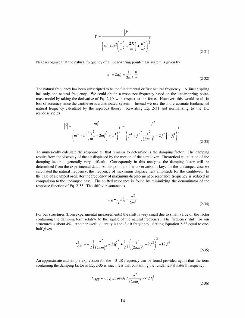
Figure 2-4. Cantilever profiles for 15 and 30 volts. The cantilever length is 100 µm and has a 0 voltageair gap of 4ʵm.
An application of 15 V is required to bend the cantilever 200 nm and 30 V bends it 1130 nm. The pitchangles are 0.11¡ and 0.64¡ respectively. The 4 µm cantilever has a much smaller bending sensitivity tovoltage than the 1 µm cantilever. A 2.5 V bias applied to the 1 µm cavity provides 68 nm of bending atthe tip. Whereas the same 2.5 V bias provides only 4.3 nm of bending for the 4 µm cavity. Recall, fromthe quadratic approximation, that the bending goes as
Bendinghco
µ12
(2-37)
This implies that a 1 µm air gap cantilever will bend 16 times more than a 4 µm cantilever for the samevoltage.
y
yhco m
hco m
= m
= m= =1
4
2
24
116
(2-38)
This suggest that the initial air gap should be minimized to provide the highest air gap change for a givenvoltage (more spectral shift). The gain in voltage sensitivity does not come at the expense of decreasedbandwidth since the bandwidth does not depend on the air gap. This is contrary to a cantilever lengthincrease which results in larger sensitivity but at the expense of a lower bandwidth. Additionally, as will bediscussed in the optical theory section, smaller cavity lengths result in a larger free spectral range.
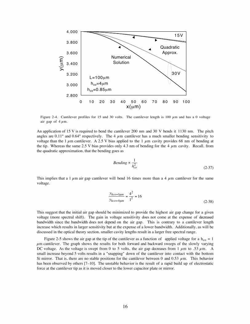
Figure 2-5 shows the air gap at the tip of the cantilever as a function of applied voltage for a hco = 1µm cantilever. The graph shows the results for both forward and backward sweeps of the slowly varyingDC voltage. As the voltage is swept from 0 to 5 volts, the air gap decreases from 1 µm to .53ʵm. Asmall increase beyond 5 volts results in a "snapping" down of the cantilever into contact with the bottomSi mirror. That is, there are no stable positions for the cantilever between 0 and 0.53 µm. This behaviorhas been observed by others [7Ð10]. The unstable behavior is the result of a rapid build up of electrostaticforce at the cantilever tip as it is moved closer to the lower capacitor plate or mirror.

17
0
0.2
0.4
0.6
0.8
1
0 1 2 3 4 5
Voltage (V)
Air
Gap
(m
m)
Quadratic Approx.
Numerical Solution
hco=1mmL=100mm
hox=0.85mm
Vth=5.1V
VR=2.72V
Sweep Direction
Figure 2-5. The position of the cantilever tip as the bias is swept in the forward and reverse directions fora hco = 1µm air gap cantilever.
The voltage for which this occurs is defined as Vth An approximation for Vth as a function of the geometryof the cantilever structure can be derived by assuming the cantilever bending quadratic as a function of lateralposition and voltage. The expression is [10]
VEh h
Lth
ox co
o=
3
10
3 3
4e (2-39)
This equation predicts Vth to be 3.9 V which is lower than that predicted by the numerical solution. Theapproximation is better for large hco/hox ratios. The snap down occurs approximately when the end of thecantilever has been bent down 1/3 of the initial air gap.
Following snap down, the voltage is swept in the reverse direction. The reverse sweep indicates a hystereticbehavior. The cantilever tip does not immediately rise as the voltage is decreased below Vth. Instead areduction of the voltage to VR = 2.71 V is required to release the cantilever (VR = release voltage). Below2.72 V the forward and reverse voltage sweeps are identical.
Figure 2-6 shows the same characteristic for the 4 µm air gap cantilever. The same hysteretic behavioris observed. The threshold voltage is a much higher 32 V which is equivalent to that predicted by thethreshold voltage equation. The release voltage is 5.77 V.
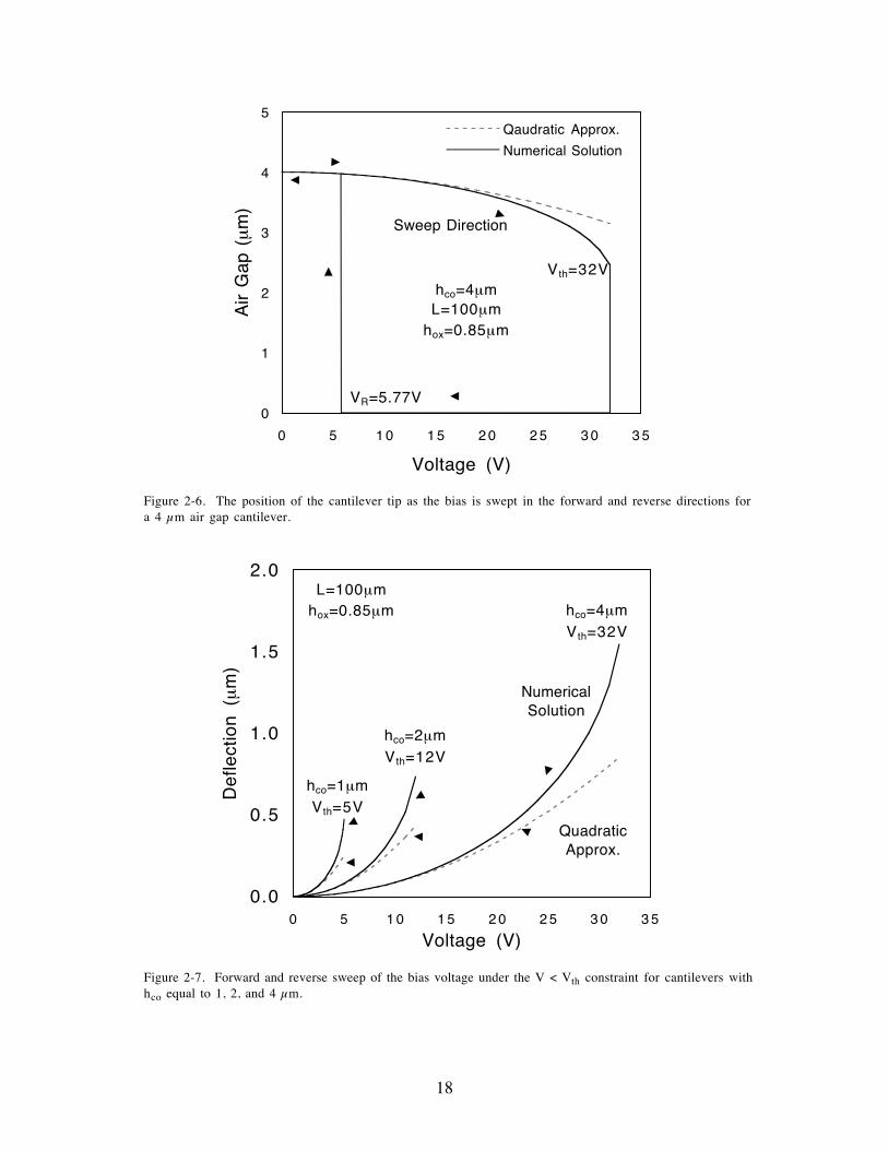
Hysteresis is generally an unwanted characteristic. Figure 2-7 shows the deflection of the cantilever tipas a function of voltage for initial air gaps of 1, 2, and 4 µm. The voltage was swept in both forward andreverse directions but not allowed to go beyond Vth. Hysteresis was not observed under this constraintVÊ<ÊVth: the curves retraced exactly. This graph also shows clearly the increased voltage sensitivity(larger slope) of the smaller air gap cantilever structures over the larger air gap cantilevers.
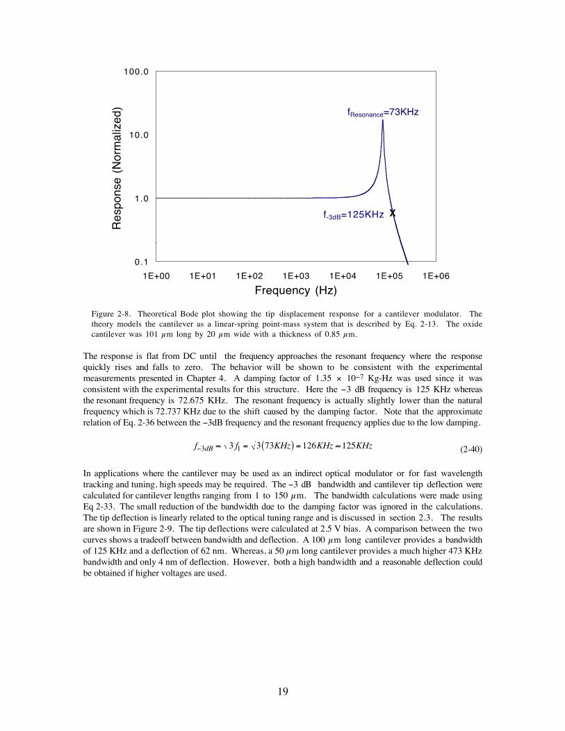
A plot of the frequency response characteristic that was calculated using Eq. 2-33 is shown inFigureÊ2-8. Here the normalized displacement response Y is plotted against drive voltage frequency. Theconstants chosen for Eq 2-13 to generate the graph were representative of one of the fabricated cantileverstructures. The oxide cantilever was 101 µm long by 20 µm wide with a thickness of 0.85 µm.
18
0
1
2
3
4
5
0 5 1 0 1 5 2 0 2 5 3 0 3 5
Voltage (V)
Air
Gap
(m
m)
Qaudratic Approx.
Numerical Solution
hco=4mmL=100mm
hox=0.85mm
Vth=32V
VR=5.77V
Sweep Direction
Figure 2-6. The position of the cantilever tip as the bias is swept in the forward and reverse directions fora 4 µm air gap cantilever.
0.0
0.5
1.0
1.5
2.0
0 5 1 0 1 5 2 0 2 5 3 0 3 5
Voltage (V)
Def
lect
ion
(mm
)
hco=1mmVth=5V
hco=2mmVth=12V
L=100mmhox=0.85mm hco=4mm
Vth=32V
NumericalSolution
QuadraticApprox.
Figure 2-7. Forward and reverse sweep of the bias voltage under the V < Vth constraint for cantilevers withhco equal to 1, 2, and 4 µm.
19
0.1
1.0
10.0
100.0
1E+00 1E+01 1E+02 1E+03 1E+04 1E+05 1E+06
Frequency (Hz)
Res
pons
e (N
orm
aliz
ed)
f-3dB=125KHz
fResonance=73KHz
X
Figure 2-8. Theoretical Bode plot showing the tip displacement response for a cantilever modulator. Thetheory models the cantilever as a linear-spring point-mass system that is described by Eq. 2-13. The oxidecantilever was 101 µm long by 20 µm wide with a thickness of 0.85 µm.
The response is flat from DC until the frequency approaches the resonant frequency where the responsequickly rises and falls to zero. The behavior will be shown to be consistent with the experimentalmeasurements presented in Chapter 4. A damping factor of 1.35 ´ 10-7 Kg-Hz was used since it wasconsistent with the experimental results for this structure. Here the -3 dB frequency is 125 KHz whereasthe resonant frequency is 72.675 KHz. The resonant frequency is actually slightly lower than the naturalfrequency which is 72.737 KHz due to the shift caused by the damping factor. Note that the approximaterelation of Eq. 2-36 between the -3dB frequency and the resonant frequency applies due to the low damping.
f f KHz KHz KHzdB- » = ( ) = »3 13 3 73 126 125 (2-40)
In applications where the cantilever may be used as an indirect optical modulator or for fast wavelengthtracking and tuning, high speeds may be required. The -3 dB bandwidth and cantilever tip deflection werecalculated for cantilever lengths ranging from 1 to 150 µm. The bandwidth calculations were made usingEq 2-33. The small reduction of the bandwidth due to the damping factor was ignored in the calculations.The tip deflection is linearly related to the optical tuning range and is discussed in section 2.3. The resultsare shown in Figure 2-9. The tip deflections were calculated at 2.5 V bias. A comparison between the twocurves shows a tradeoff between bandwidth and deflection. A 100 µm long cantilever provides a bandwidthof 125 KHz and a deflection of 62 nm. Whereas, a 50 µm long cantilever provides a much higher 473ÊKHzbandwidth and only 4 nm of deflection. However, both a high bandwidth and a reasonable deflection couldbe obtained if higher voltages are used.
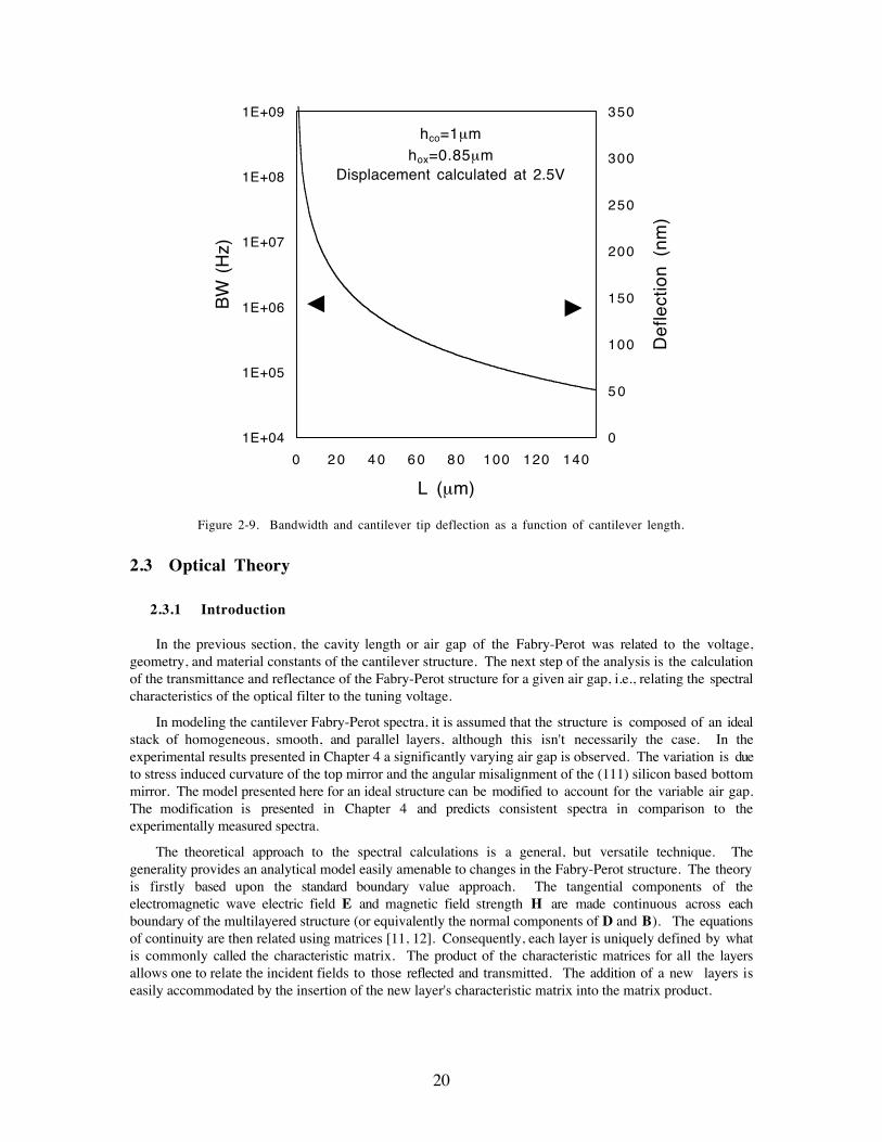
20
1E+04
1E+05
1E+06
1E+07
1E+08
1E+09
0 2 0 4 0 6 0 8 0 100 120 140
L (mm)
BW
(H
z)
0
5 0
100
150
200
250
300
350
Def
lect
ion
(nm
)
hco=1mmhox=0.85mm
Displacement calculated at 2.5V
Figure 2-9. Bandwidth and cantilever tip deflection as a function of cantilever length.
2.3 Optical Theory
2.3.1 Introduction
In the previous section, the cavity length or air gap of the Fabry-Perot was related to the voltage,geometry, and material constants of the cantilever structure. The next step of the analysis is the calculationof the transmittance and reflectance of the Fabry-Perot structure for a given air gap, i.e., relating the spectralcharacteristics of the optical filter to the tuning voltage.
In modeling the cantilever Fabry-Perot spectra, it is assumed that the structure is composed of an idealstack of homogeneous, smooth, and parallel layers, although this isn't necessarily the case. In theexperimental results presented in Chapter 4 a significantly varying air gap is observed. The variation is dueto stress induced curvature of the top mirror and the angular misalignment of the (111) silicon based bottommirror. The model presented here for an ideal structure can be modified to account for the variable air gap.The modification is presented in Chapter 4 and predicts consistent spectra in comparison to theexperimentally measured spectra.
The theoretical approach to the spectral calculations is a general, but versatile technique. Thegenerality provides an analytical model easily amenable to changes in the Fabry-Perot structure. The theoryis firstly based upon the standard boundary value approach. The tangential components of theelectromagnetic wave electric field E and magnetic field strength H are made continuous across eachboundary of the multilayered structure (or equivalently the normal components of D and B). The equationsof continuity are then related using matrices [11, 12]. Consequently, each layer is uniquely defined by whatis commonly called the characteristic matrix. The product of the characteristic matrices for all the layersallows one to relate the incident fields to those reflected and transmitted. The addition of a new layers iseasily accommodated by the insertion of the new layer's characteristic matrix into the matrix product.
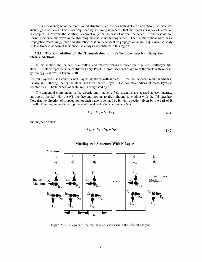
21
The spectral analysis of the multilayered structure is correct for both dielectric and absorptive materialssuch as gold or nickel. This is accomplished by assuming in general, that the materials index of refractionis complex. However, the solution is correct only for the case of normal incidence. In the case of nonnormal incidence, the wave in the absorbing material is nonhomogeneous. That is, the optical wave has apropagation vector magnitude and absorption that are dependent on propagation angle [13]. Since the studyin its entirety is at normal incidence, the analysis is confined to this region.
2.3.2 The Calculation of the Transmission and Reflectance Spectra Using theMatrix Method
In this section, the incident, transmitted, and reflected fields are related for a general multilayer filmstack. The stack represents the cantilever Fabry-Perot. A cross-sectional diagram of the stack with relevantsymbology is shown in Figure 2-10.
The multilayered stack consists of N layers identified with indices: 0 for the incidence medium which isusually air, 1 through N for the stack, and l for the last layer. The complex indices of these layers isdenoted by n. The thickness of each layer is designated by h.
The tangential components of the electric and magnetic field strengths are equated at each interfacestarting on the left with the 0/1 interface and moving to the right and concluding with the N/l interface.Note that the direction of propagation for each wave is denoted by K with direction given by the curl of Einto H. Equating tangential components of the electric fields at the interface
E E E Er i r i0 0 1 1+ = + (2-41)
and magnetic fields:
H H H Hr i r i0 0 1 1- = - (2-42)
Medium
0 1 2
. . .
N L
IncidentMedium
TransmissionMedium
Multilayered Structure With N Layers
h1 h2
E0r
H0r
K0i
H0i
E0i
K0r
E1r
H1r
K1r
E2r
H2r
K2r
ENr
HNr
KNr
K1i
H1i
E1i
K2i
H2i
E2iKNi
HNi
ENi
Kli
Hli
Eli
Än1 Än2 ÄnNÄn0 Änl
Figure 2-10. Diagram of the multilayered stack used in the spectral analysis.
22
The relation between E and H for a plane wave is given by
Hn
Em
o=Ä
h (2-43)
Än mthlayer complex index
freespace waveimpedencem
o
®
®h
Substituting into the H field continuity expression
® - = -E n E n E n E nr i r i0 0 0 0 1 1 1 1Ä Ä Ä Ä (2-44)
These two equations describing the 0/1 interface can be rewritten in matrix form as
R A L A0 0 1 1= (2-45)
Rn n
AE
EL
n nA
E
Er
i
r
i0
0 00
0
01
1 11
1
1
1 1 1 1=
-æ
èç
ö
ø÷ =
æ
èç
ö
ø÷ =
-æ
èç
ö
ø÷ =
æ
èç
ö
ø÷Ä Ä
, ,Ä Ä
, (2-46)
For the next boundary, 1/2 , the continuity equations become trickier since the relative phase shifts for thewaves must be included.
E e E e E Erj
ij
r i1 1 2 21 1- + = +b b
(2-47)
E n e E n e E n E nrj
ij
r i1 1 1 1 2 2 2 21 1Ä Ä Ä Ä- - = -b b
(2-48)
The phase shift b is given by:
bl
l
m m m
m
h n
freespace wavelength
h mthlayer thickness
=
®
®
2P Ä
(2-49)
Note that the forward moving wave in medium 1 is advanced in phase by b in propagating from the 0/1 tothe 1/2 interface. Similarly, the backward traveling wave in medium 1 is retarded in phase by b in goingfrom interface 0/1 to 1/2. The matrix relation for the 1/2 interface is given by
R A L A1 1 2 2= (2-50)
Re e
n e n eA
E
EL
n nA
E
E
j j
j jr
i
r
i1
0 01
1
12
2 22
2
2
1 1
1 1
1 1=
-
æ
èç
ö
ø÷ =
æ
èç
ö
ø÷ =
-æ
èç
ö
ø÷ =
æ
èç
ö
ø÷
-
-
b b
b bÄ Ä, ,
Ä Ä,
(2-51)
23
Similar matrix relations can be generated for each layer in the stack. For the last layer of the stack denotedby l.
R A L AN N l l= (2-52)
Re e
n e n eA
E
EL
n nA
E
EN
j j
Nj
Nj N
Nr
Nil
l ll
lr
li
N N
N N=
-
æ
èç
ö
ø÷ =
æ
èç
ö
ø÷ =
-æ
èç
ö
ø÷ =
æ
èç
ö
ø÷
-
-
b b
b bÄ Ä, ,
Ä Ä,
1 1
(2-53)
For the complete stack we can write using the inverse matrix operation
R A L R L R L R L RN N l l0 0 1 112 2
1 1= · · ·[ ]- - - (2-54)
Note that the matrix product in the brackets is a product of characteristic matrices for each layer. Theproduct can be rewritten as
R A M M M L AN l l0 0 1 2= · · ·[ ] (2-55)
M L Rm m m= -1 (2-56)
Here Mm is the characteristic matrix of each layer. The matrix product of the layers shown in brackets ismultiplied and represented by MT the characteristic matrix of the total stack.
Mm
m
m
mT =æ
èç
ö
ø÷
11
21
12
22(2-57)
R A M L AT l l0 0 = (2-58)
After the elements of the matrix have been calculated with a computer program, they can be used tocalculate the field transmittance and reflectance using the easily derived equations below [11].
rE
E
n m m n m n m
n m m n m n mor
oi
l l
l l= =
-( ) - -( )-( ) + -( )
Ä Ä Ä
Ä Ä Ä0 11 12 22 21
0 11 12 22 21 (2-59)
tE
E
n
n m m n m n mli
oi l l= =
-( ) + -( )2 0
0 11 12 22 21
Ä
Ä Ä Ä(2-60)
The power reflectance and transmittance are given by
R r= 2(2-61)
Tn
ntl=
0
2
(2-62)
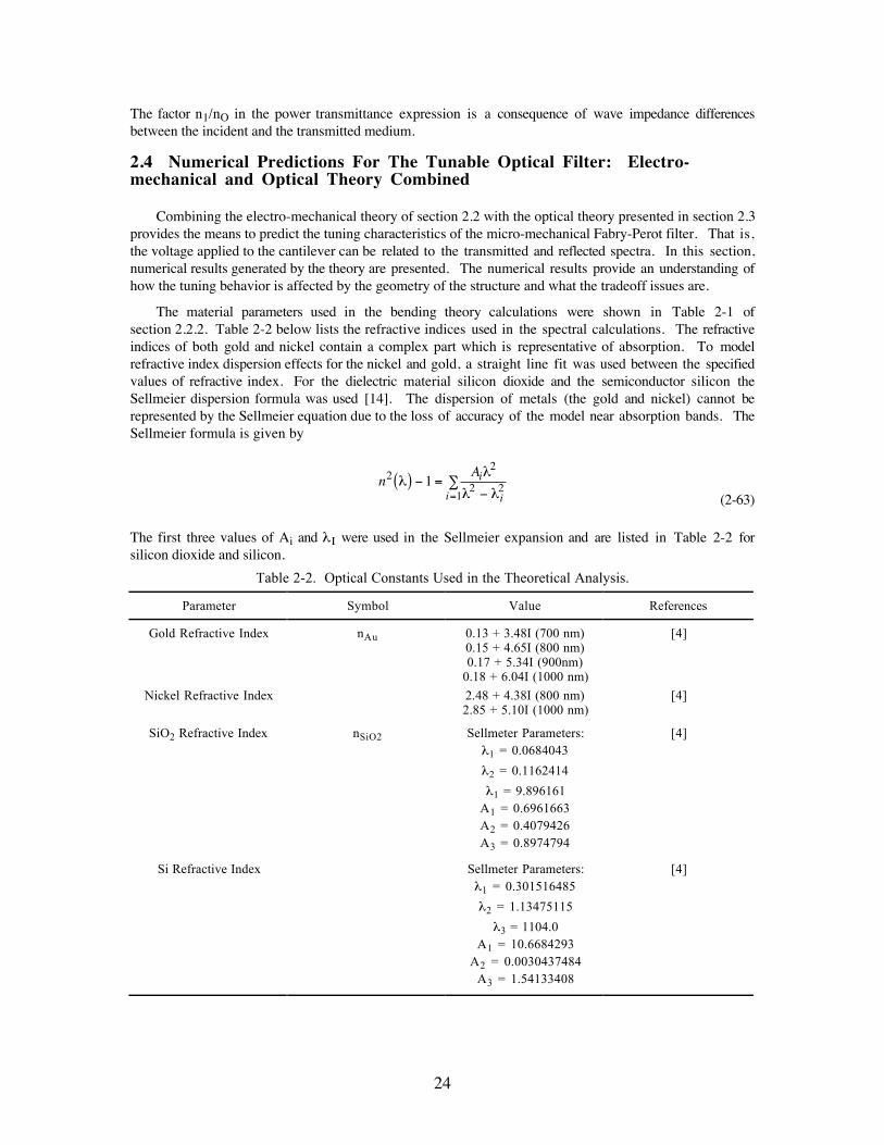
24
The factor n1/nO in the power transmittance expression is a consequence of wave impedance differencesbetween the incident and the transmitted medium.
2.4 Numerical Predictions For The Tunable Optical Filter: Electro-mechanical and Optical Theory Combined
Combining the electro-mechanical theory of section 2.2 with the optical theory presented in section 2.3provides the means to predict the tuning characteristics of the micro-mechanical Fabry-Perot filter. That is,the voltage applied to the cantilever can be related to the transmitted and reflected spectra. In this section,numerical results generated by the theory are presented. The numerical results provide an understanding ofhow the tuning behavior is affected by the geometry of the structure and what the tradeoff issues are.
The material parameters used in the bending theory calculations were shown in Table 2-1 ofsectionÊ2.2.2. Table 2-2 below lists the refractive indices used in the spectral calculations. The refractiveindices of both gold and nickel contain a complex part which is representative of absorption. To modelrefractive index dispersion effects for the nickel and gold, a straight line fit was used between the specifiedvalues of refractive index. For the dielectric material silicon dioxide and the semiconductor silicon theSellmeier dispersion formula was used [14]. The dispersion of metals (the gold and nickel) cannot berepresented by the Sellmeier equation due to the loss of accuracy of the model near absorption bands. TheSellmeier formula is given by
nAi
ii
22
2 21
1ll
l l( ) - =
-å= (2-63)
The first three values of Ai and lI were used in the Sellmeier expansion and are listed in Table 2-2 forsilicon dioxide and silicon.
Table 2-2. Optical Constants Used in the Theoretical Analysis.
Parameter Symbol Value References
Gold Refractive Index nAu 0.13 + 3.48I (700 nm)0.15 + 4.65I (800 nm)0.17 + 5.34I (900nm)
0.18 + 6.04I (1000 nm)
[4]
Nickel Refractive Index 2.48 + 4.38I (800 nm)2.85 + 5.10I (1000 nm)
[4]
SiO2 Refractive Index nSiO2 Sellmeter Parameters:l1 = 0.0684043
l2 = 0.1162414
l1 = 9.896161A1 = 0.6961663A2 = 0.4079426A3 = 0.8974794
[4]
Si Refractive Index Sellmeter Parameters:l1 = 0.301516485
l2 = 1.13475115
l3 = 1104.0A1 = 10.6684293
A2 = 0.0030437484A3 = 1.54133408
[4]
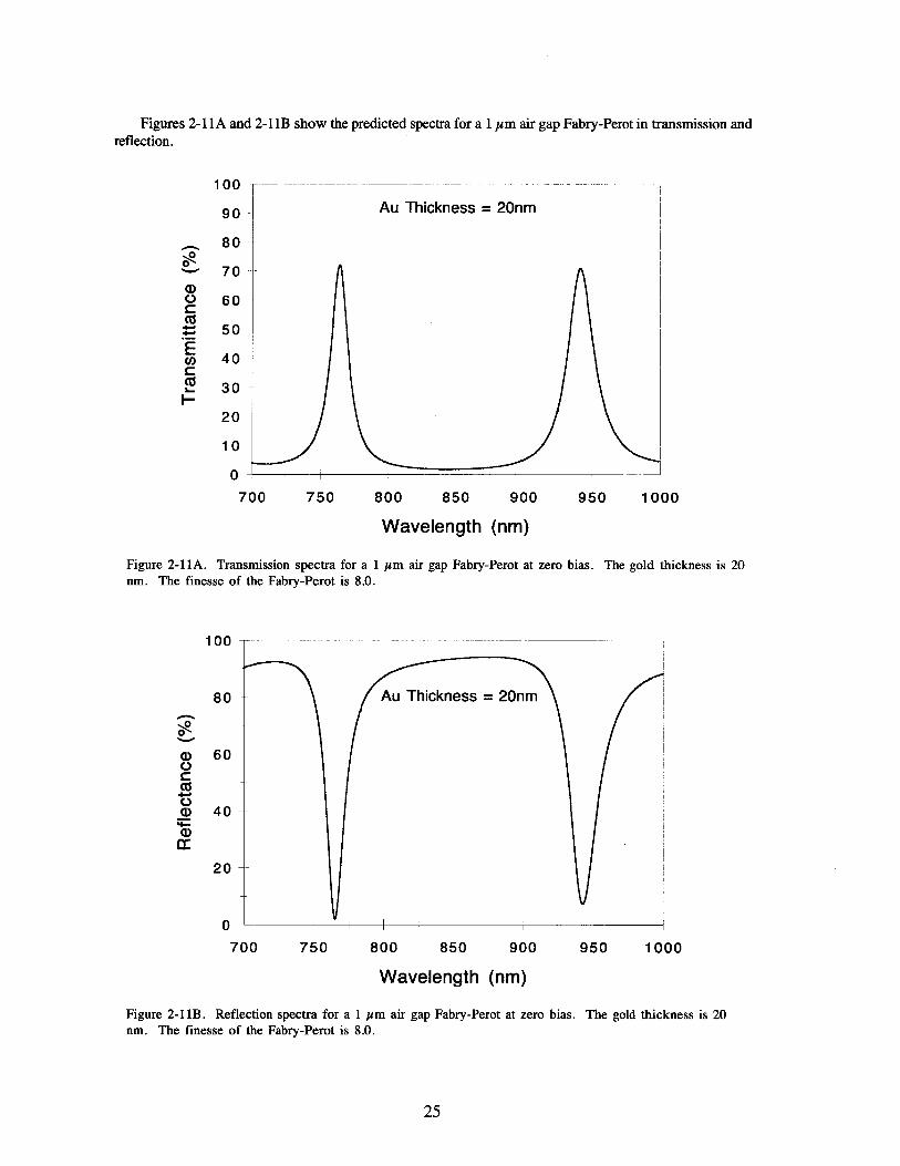
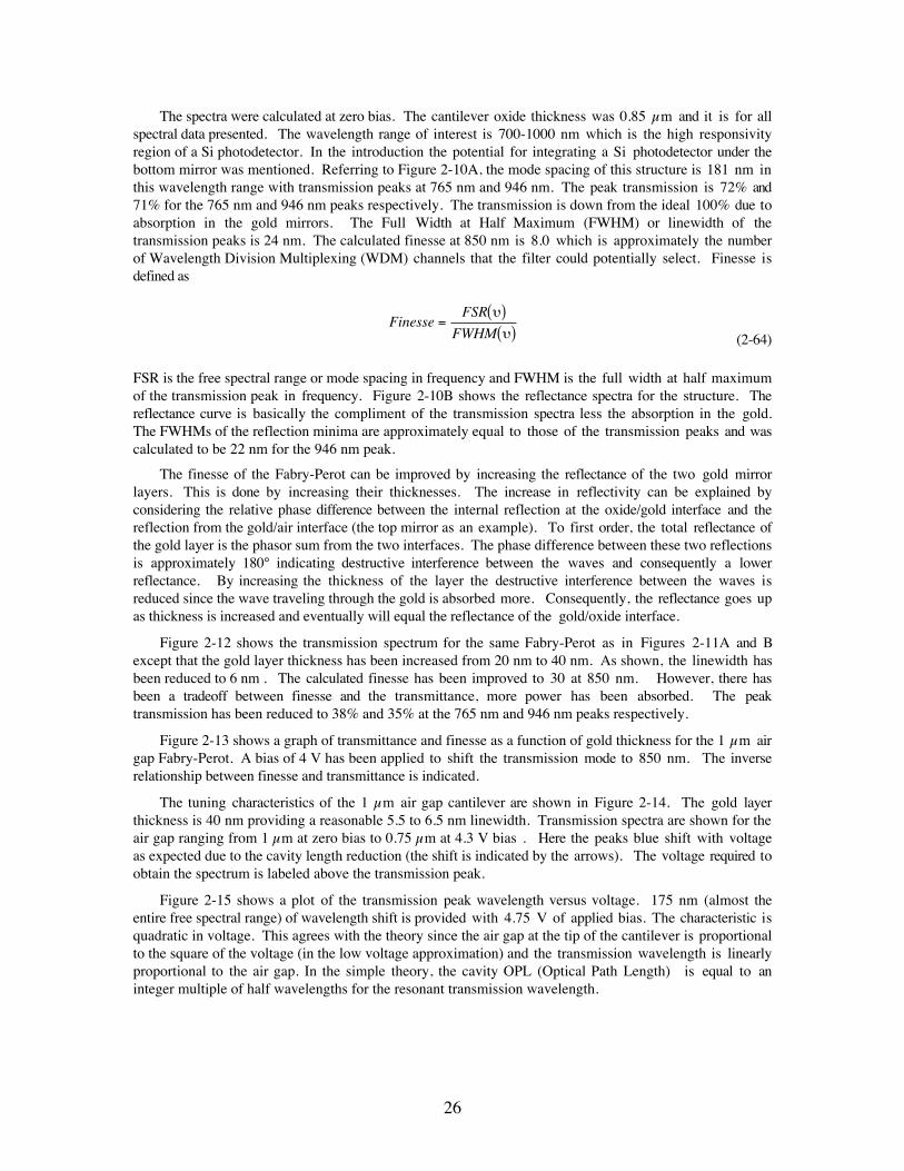
26
The spectra were calculated at zero bias. The cantilever oxide thickness was 0.85 µm and it is for allspectral data presented. The wavelength range of interest is 700-1000 nm which is the high responsivityregion of a Si photodetector. In the introduction the potential for integrating a Si photodetector under thebottom mirror was mentioned. Referring to Figure 2-10A, the mode spacing of this structure is 181 nm inthis wavelength range with transmission peaks at 765 nm and 946 nm. The peak transmission is 72% and71% for the 765 nm and 946 nm peaks respectively. The transmission is down from the ideal 100% due toabsorption in the gold mirrors. The Full Width at Half Maximum (FWHM) or linewidth of thetransmission peaks is 24 nm. The calculated finesse at 850 nm is 8.0 which is approximately the numberof Wavelength Division Multiplexing (WDM) channels that the filter could potentially select. Finesse isdefined as
FinesseFSR
FWHM=
( )( )
u
u (2-64)
FSR is the free spectral range or mode spacing in frequency and FWHM is the full width at half maximumof the transmission peak in frequency. Figure 2-10B shows the reflectance spectra for the structure. Thereflectance curve is basically the compliment of the transmission spectra less the absorption in the gold.The FWHMs of the reflection minima are approximately equal to those of the transmission peaks and wascalculated to be 22 nm for the 946 nm peak.
The finesse of the Fabry-Perot can be improved by increasing the reflectance of the two gold mirrorlayers. This is done by increasing their thicknesses. The increase in reflectivity can be explained byconsidering the relative phase difference between the internal reflection at the oxide/gold interface and thereflection from the gold/air interface (the top mirror as an example). To first order, the total reflectance ofthe gold layer is the phasor sum from the two interfaces. The phase difference between these two reflectionsis approximately 180¡ indicating destructive interference between the waves and consequently a lowerreflectance. By increasing the thickness of the layer the destructive interference between the waves isreduced since the wave traveling through the gold is absorbed more. Consequently, the reflectance goes upas thickness is increased and eventually will equal the reflectance of the gold/oxide interface.
Figure 2-12 shows the transmission spectrum for the same Fabry-Perot as in Figures 2-11A and Bexcept that the gold layer thickness has been increased from 20 nm to 40 nm. As shown, the linewidth hasbeen reduced to 6 nm . The calculated finesse has been improved to 30 at 850 nm. However, there hasbeen a tradeoff between finesse and the transmittance, more power has been absorbed. The peaktransmission has been reduced to 38% and 35% at the 765 nm and 946 nm peaks respectively.
Figure 2-13 shows a graph of transmittance and finesse as a function of gold thickness for the 1 µm airgap Fabry-Perot. A bias of 4 V has been applied to shift the transmission mode to 850 nm. The inverserelationship between finesse and transmittance is indicated.
The tuning characteristics of the 1 µm air gap cantilever are shown in Figure 2-14. The gold layerthickness is 40 nm providing a reasonable 5.5 to 6.5 nm linewidth. Transmission spectra are shown for theair gap ranging from 1 µm at zero bias to 0.75 µm at 4.3 V bias . Here the peaks blue shift with voltageas expected due to the cavity length reduction (the shift is indicated by the arrows). The voltage required toobtain the spectrum is labeled above the transmission peak.
Figure 2-15 shows a plot of the transmission peak wavelength versus voltage. 175 nm (almost theentire free spectral range) of wavelength shift is provided with 4.75 V of applied bias. The characteristic isquadratic in voltage. This agrees with the theory since the air gap at the tip of the cantilever is proportionalto the square of the voltage (in the low voltage approximation) and the transmission wavelength is linearlyproportional to the air gap. In the simple theory, the cavity OPL (Optical Path Length) is equal to aninteger multiple of half wavelengths for the resonant transmission wavelength.

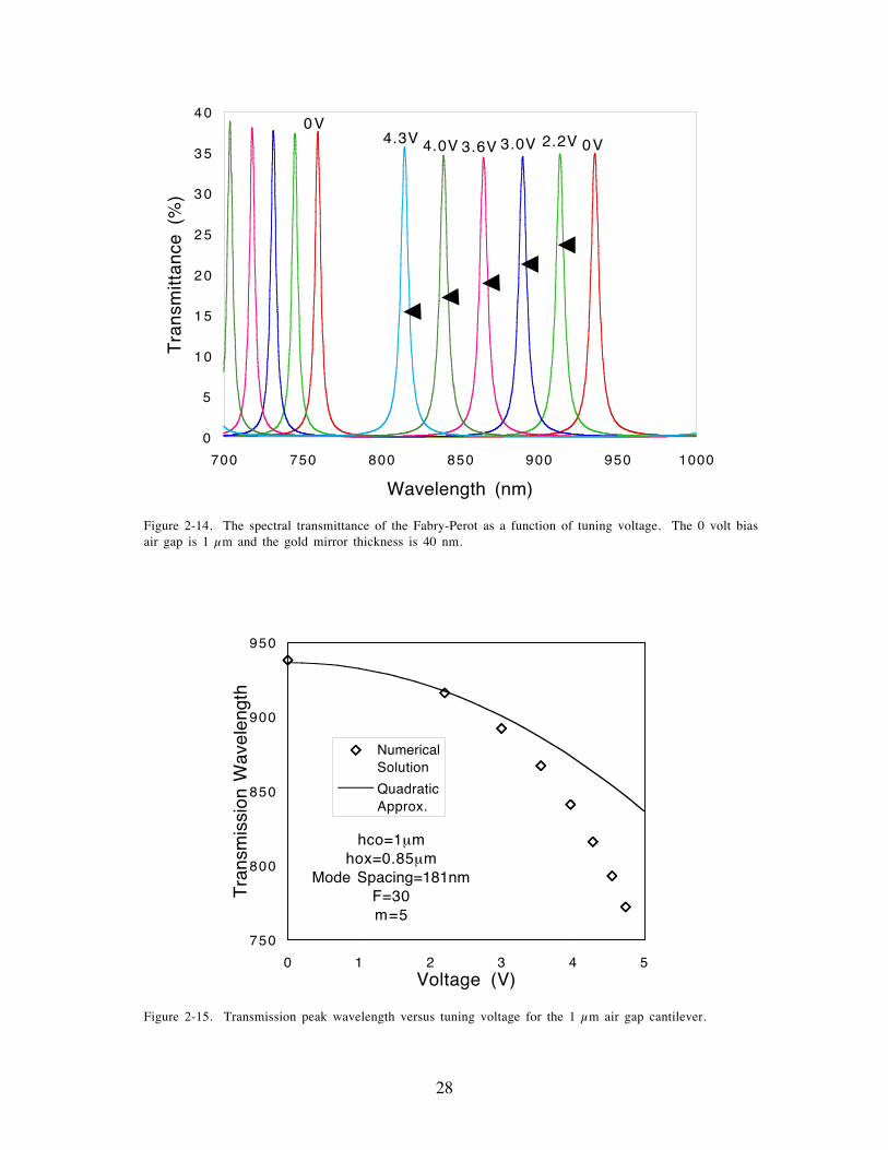
28
0
5
1 0
1 5
2 0
2 5
3 0
3 5
4 0
700 750 800 850 900 950 1000
Wavelength (nm)
Tra
nsm
ittan
ce (
%)
0V2.2V3.0V3.6V4.0V4.3V0V
Figure 2-14. The spectral transmittance of the Fabry-Perot as a function of tuning voltage. The 0 volt biasair gap is 1 µm and the gold mirror thickness is 40 nm.
750
800
850
900
950
0 1 2 3 4 5Voltage (V)
Tra
nsm
issi
on W
avel
engt
h
NumericalSolution
QuadraticApprox.
hco=1mmhox=0.85mm
Mode Spacing=181nmF=30m=5
Figure 2-15. Transmission peak wavelength versus tuning voltage for the 1 µm air gap cantilever.

29
OPL m n h h
m positiveinteger
n oxiderefractiveindex
h oxidethickness
h air gap
SiO ox c
SiO
ox
c
= = +
®
®
®
®
l
2 2
2
(2-65)
Using this relation in conjunction with the quadratic approximation in section 2.2.1 results in
le
e
Vm
n h hEh
V
hh
LSiO ox coo
oxco
ox
rox
( ) = + -
+é
ëê
ù
ûú
ì
í
ïï
î
ïï
ü
ý
ïï
þ
ïï
2 3
42 3
2
24
(2-66)
This approximation was plotted along with the numerical solution. The approximation predicts thecharacteristic closely up to 3 V. Beyond 3 V the analytic approximation underestimates the wavelengthshift. The reduced accuracy beyond 3 V is due to the inaccuracy of the quadratic approximation of thecantilever bending at high values of the voltage to air gap ratio.
Figures 2-16 shows the transmission spectra for a 4 µm air gap cantilever with zero bias. The modespacing is a much smaller 73 nm in comparison to the 181 nm of the 1 µm air gap Fabry-Perot. This ispredicted by the simple theory
frequency mode spacing: Df
c
OPL=2 (2-67)
Wavelength Mode Spacing: DD
ll l
= »2 2
2
f
c OPL(2-68)
However, consistent with a constant finesse (the finesse depends only on the mirror reflectances), thelinewidth of the 4 µm cavity is smaller by the factor 73/181. In agreement the linewidth is 2.3 nm at the887 nm peak.
The smaller linewidth of the 4 µm structure could be more advantageous over the shorter 1 µm Fabry-Perot in applications where the spectral lines of the source are closely spaced and a large free spectral rangeis not required.
Figure 2-17 shows the spectra for the 4 µm cavity for voltages ranging from 0 to 16.6 V. Thetransmission spectra linewidths range from 1.8 to 2.3 nm.
Figure 2-18 shows the transmission peak wavelength as a function of tuning voltage. The samequadratic behavior is observed as with the 1 µm air gap cavity. However, the wavelength shift sensitivityto voltage in much reduced. A wavelength shift of 71 nm is obtained with 20.5 V whereas the 1ʵmcavity provided 166 nm of tuning with only 4.7 V. The quadratic approximation more accurately predictsthe tuning behavior of the 4 µm air gap cantilever due its small voltage to air gap ratio in comparison tothe 1 µm structure .
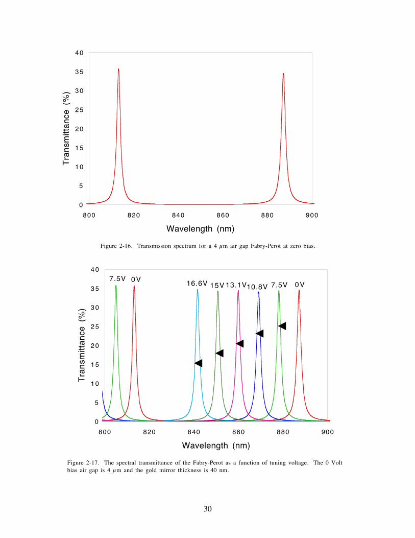
30
0
5
1 0
1 5
2 0
2 5
3 0
3 5
4 0
800 820 840 860 880 900
Wavelength (nm)
Tra
nsm
ittan
ce (
%)
Figure 2-16. Transmission spectrum for a 4 µm air gap Fabry-Perot at zero bias.
0
5
1 0
1 5
2 0
2 5
3 0
3 5
4 0
800 820 840 860 880 900
Wavelength (nm)
Tra
nsm
ittan
ce (
%)
0V7.5V10.8V13.1V15V16.6V0V7.5V
Figure 2-17. The spectral transmittance of the Fabry-Perot as a function of tuning voltage. The 0 Voltbias air gap is 4 µm and the gold mirror thickness is 40 nm.
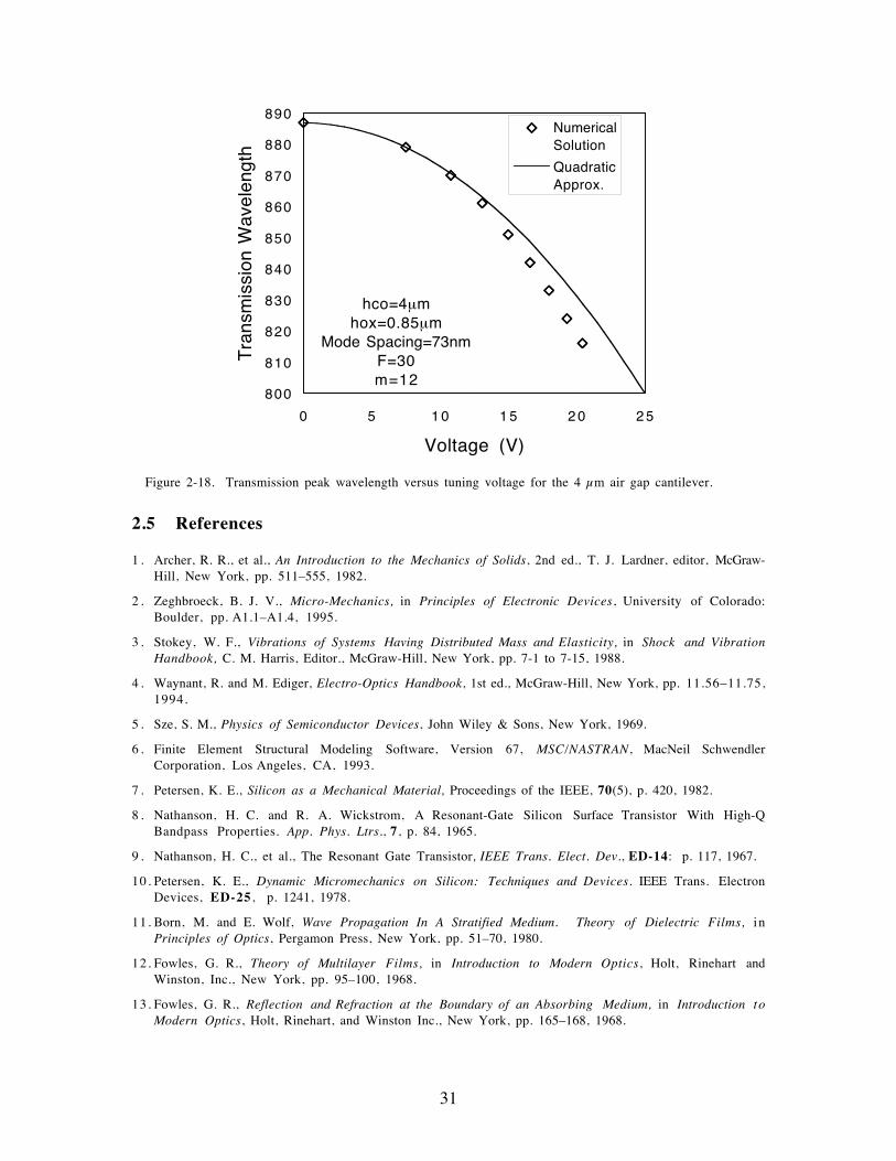
31
800
810
820
830
840
850
860
870
880
890
0 5 1 0 1 5 2 0 2 5
Voltage (V)
Tra
nsm
issi
on W
avel
engt
h
NumericalSolution
QuadraticApprox.
hco=4mmhox=0.85mm
Mode Spacing=73nmF=30m=12
Figure 2-18. Transmission peak wavelength versus tuning voltage for the 4 µm air gap cantilever.
2.5 References
1 . Archer, R. R., et al., An Introduction to the Mechanics of Solids, 2nd ed., T. J. Lardner, editor, McGraw-Hill, New York, pp. 511Ð555, 1982.
2 . Zeghbroeck, B. J. V., Micro-Mechanics, in Principles of Electronic Devices, University of Colorado:Boulder, pp.ÊA1.1ÐA1.4, 1995.
3 . Stokey, W. F., Vibrations of Systems Having Distributed Mass and Elasticity, in Shock and VibrationHandbook, C. M. Harris, Editor., McGraw-Hill, New York, pp. 7-1 to 7-15, 1988.
4 . Waynant, R. and M. Ediger, Electro-Optics Handbook, 1st ed., McGraw-Hill, New York, pp. 11.56Ð11.75,1994.
5 . Sze, S. M., Physics of Semiconductor Devices, John Wiley & Sons, New York, 1969.
6 . Finite Element Structural Modeling Software, Version 67, MSC/NASTRAN, MacNeil SchwendlerCorporation, LosÊAngeles, CA, 1993.
7 . Petersen, K. E., Silicon as a Mechanical Material, Proceedings of the IEEE, 70(5), p. 420, 1982.
8 . Nathanson, H. C. and R. A. Wickstrom, A Resonant-Gate Silicon Surface Transistor With High-QBandpass Properties. App. Phys. Ltrs., 7, p. 84, 1965.
9 . Nathanson, H. C., et al., The Resonant Gate Transistor, IEEE Trans. Elect. Dev., ED-14: p. 117, 1967.
10. Petersen, K. E., Dynamic Micromechanics on Silicon: Techniques and Devices. IEEE Trans. ElectronDevices, ED-25 , p. 1241, 1978.
11. Born, M. and E. Wolf, Wave Propagation In A Stratified Medium. Theory of Dielectric Films, inPrinciples of Optics, Pergamon Press, New York, pp. 51Ð70, 1980.
12. Fowles, G. R., Theory of Multilayer Films, in Introduction to Modern Optics, Holt, Rinehart andWinston, Inc., New York, pp. 95Ð100, 1968.
13. Fowles, G. R., Reflection and Refraction at the Boundary of an Absorbing Medium, in Introduction toModern Optics, Holt, Rinehart, and Winston Inc., New York, pp. 165Ð168, 1968.
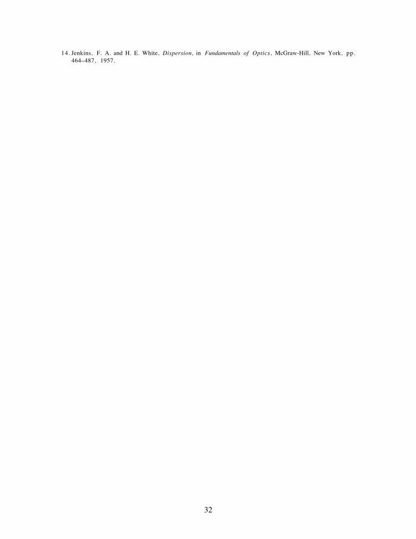
32
14. Jenkins, F. A. and H. E. White, Dispersion, in Fundamentals of Optics, McGraw-Hill, New York, pp.464Ð487, 1957.
33
III. Fabrication of the Micro-Mechanical Fabry-Perot Filters
3.0 Introduction.
In this chapter we present an overview of the standard methods used to fabricate micro-mechanicalFabry-Perots. This is followed by a section discussing silicon micro-machining using anisotropic wetKOH etching and Reactive Ion Etching (RIE). A combination of vertical RIE and wet KOH etching isshown to provide lateral etching in (111) silicon which can be used to undercut a silicon dioxide or siliconnitride masking material. In section 3.3 we introduce a new fabrication process to form air gap micro-mechanical Fabry-Perots that is based on this etching technique. Fabry-Perots formed with this techniqueare the focus of the study. Finally in section 3.4 we describe the entire fabrication process in detail. Theprocess presented is self-aligned and uses only one mask level to provide the mirrors and the electricalisolation. Fabrication results, problems, and potential solutions are also presented.
3.1 Popular Methods of Micro-Mechanical Fabry-Perot Fabrication UsingDeposited Materials
The fabrication methods for micro-mechanical Fabry-Perots recently reported in the literature rely ondeposited materials for the mirrors and the air gap formation. In general, these methods require theformation of a sandwich of mirror material surrounding a sacrificial layer that can be removed selectivelyproducing an air gap Fabry-Perot. This is accomplished by depositing the bottom mirror material on thesubstrate, followed by a sacrificial layer, and then the top mirror. These layers are typically deposited byChemical Vapor Deposition (CVD) or Molecular Beam Epitaxy (MBE) processes. Via holes for a wetchemical or plasma etchant are provided through the top mirror region to facilitate the removal of thesacrificial layer. Removal of the sacrificial layer can be accomplished by both wet chemical and plasmaetchants provided that the etchant has a high selectivity to the sacrificial layer over the mirror materials.
Polyimide and photoresist have been used successfully as a sacrificial layer when using Si and SiO2DBR mirrors [1]. The polyimide or photoresist are easily removed with an oxygen plasma withoutattacking Si or SiO2. Acetone can be used to remove the positive photoresist also. Researchers fabricatingGaAs based Fabry-Perots have used intrinsic GaAs as a sacrificial layer with AlGaAs mirrors. Selectiveremoval of the GaAs sacrificial layer has been accomplished with a dry etch using a SiCl4 and SF6 plasma[2].
3.2 Anisotropic Etching of Silicon in KOH
Another method of sacrificial layer removal is to take advantage of the anisotropic etching behavior of acrystalline material in a wet chemical. This process is simpler, since the sacrificial layer need not bedeposited. Instead the substrate material provides the sacrificial layer. In this section we present anoverview of anisotropic etching of Si in KOH and an associated method by which thin film membranes canbe undercut. The method is amenable to the fabrication of micro-mechanical Fabry-Perot structures.
The anisotropic etching behavior of crystalline silicon in wet chemical etchants has been known formany years [3Ð6]. This anisotropy makes possible many unique etched geometries. Integrated circuitdesigns have implemented anisotropic etching to form trench electrical isolation around transistors. In thearea of micro-machining, pyramid shaped ink jet nozzles have been formed using the anisotropic etchingbehavior. The anisotropic etching behavior is a consequence of a high etch rate dependency on direction inthe silicon crystal. This dependence has been attributed to differences in atomic and dangling bond densitiesfor different planes in the crystalline lattice [3]. In the silicon lattice, the principle feature of theanisotropic etching behavior is the much slower etch rate of the (111) planes in comparison to the muchfaster etching (110) and (100) planes. The (111) planes have the highest density of atoms per squarecentimeter and the lowest density of dangling bonds that can be easily attacked by the etchant molecules.
A common anisotropic silicon etchant is KOH. Its silicon etching behavior has been well studied
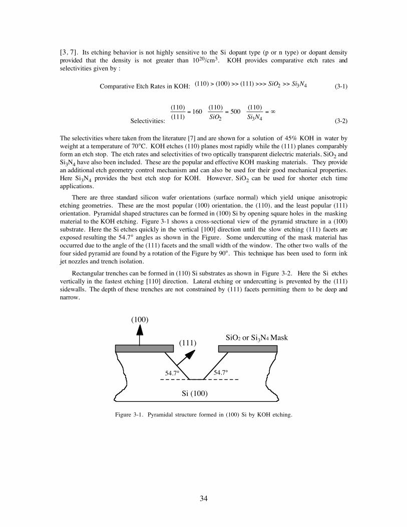
34
[3,Ê7]. Its etching behavior is not highly sensitive to the Si dopant type (p or n type) or dopant densityprovided that the density is not greater than 1020/cm3. KOH provides comparative etch rates andselectivities given by :
Comparative Etch Rates in KOH: ( ) ( ) ( )110 100 111 2 3 4> >> >>> >>SiO Si N (3-1)
Selectivities:
( )
( )
( ) ( )110
111160
110500
110
2 3 4= = = ¥
SiO Si N(3-2)
The selectivities where taken from the literature [7] and are shown for a solution of 45% KOH in water byweight at a temperature of 70°C. KOH etches (110) planes most rapidly while the (111) planes comparablyform an etch stop. The etch rates and selectivities of two optically transparent dielectric materials, SiO2 andSi3N4 have also been included. These are the popular and effective KOH masking materials. They providean additional etch geometry control mechanism and can also be used for their good mechanical properties.Here Si3N4 provides the best etch stop for KOH. However, SiO2 can be used for shorter etch timeapplications.
There are three standard silicon wafer orientations (surface normal) which yield unique anisotropicetching geometries. These are the most popular (100) orientation, the (110), and the least popular (111)orientation. Pyramidal shaped structures can be formed in (100) Si by opening square holes in the maskingmaterial to the KOH etching. Figure 3-1 shows a cross-sectional view of the pyramid structure in a (100)substrate. Here the Si etches quickly in the vertical [100] direction until the slow etching (111) facets areexposed resulting the 54.7° angles as shown in the Figure. Some undercutting of the mask material hasoccurred due to the angle of the (111) facets and the small width of the window. The other two walls of thefour sided pyramid are found by a rotation of the Figure by 90°. This technique has been used to form inkjet nozzles and trench isolation.
Rectangular trenches can be formed in (110) Si substrates as shown in Figure 3-2. Here the Si etchesvertically in the fastest etching [110] direction. Lateral etching or undercutting is prevented by the (111)sidewalls. The depth of these trenches are not constrained by (111) facets permitting them to be deep andnarrow.
Si (100)
54.7¡ 54.7¡
SiO2 or Si3N4 Mask(111)
(100)
Figure 3-1. Pyramidal structure formed in (100) Si by KOH etching.
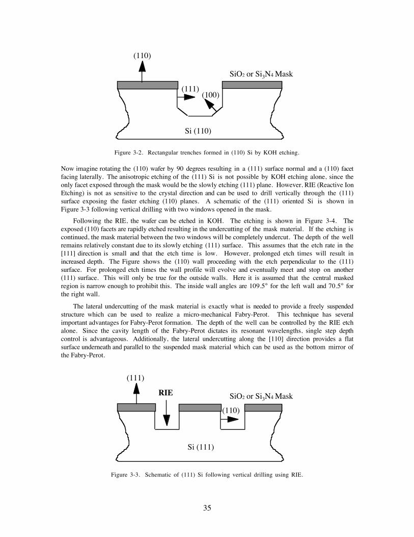
35
Si (110)
SiO2 or Si3N4 Mask
(111)
(110)
(100)
Figure 3-2. Rectangular trenches formed in (110) Si by KOH etching.
Now imagine rotating the (110) wafer by 90 degrees resulting in a (111) surface normal and a (110) facetfacing laterally. The anisotropic etching of the (111) Si is not possible by KOH etching alone, since theonly facet exposed through the mask would be the slowly etching (111) plane. However, RIE (Reactive IonEtching) is not as sensitive to the crystal direction and can be used to drill vertically through the (111)surface exposing the faster etching (110) planes. A schematic of the (111) oriented Si is shown inFigureÊ3-3 following vertical drilling with two windows opened in the mask.
Following the RIE, the wafer can be etched in KOH. The etching is shown in Figure 3-4. Theexposed (110) facets are rapidly etched resulting in the undercutting of the mask material. If the etching iscontinued, the mask material between the two windows will be completely undercut. The depth of the wellremains relatively constant due to its slowly etching (111) surface. This assumes that the etch rate in the[111] direction is small and that the etch time is low. However, prolonged etch times will result inincreased depth. The Figure shows the (110) wall proceeding with the etch perpendicular to the (111)surface. For prolonged etch times the wall profile will evolve and eventually meet and stop on another(111) surface. This will only be true for the outside walls. Here it is assumed that the central maskedregion is narrow enough to prohibit this. The inside wall angles are 109.5° for the left wall and 70.5° forthe right wall.
The lateral undercutting of the mask material is exactly what is needed to provide a freely suspendedstructure which can be used to realize a micro-mechanical Fabry-Perot. This technique has severalimportant advantages for Fabry-Perot formation. The depth of the well can be controlled by the RIE etchalone. Since the cavity length of the Fabry-Perot dictates its resonant wavelengths, single step depthcontrol is advantageous. Additionally, the lateral undercutting along the [110] direction provides a flatsurface underneath and parallel to the suspended mask material which can be used as the bottom mirror ofthe Fabry-Perot.
(111)
Si (111)
SiO2 or Si3N4 Mask
(110)
RIE
Figure 3-3. Schematic of (111) Si following vertical drilling using RIE.
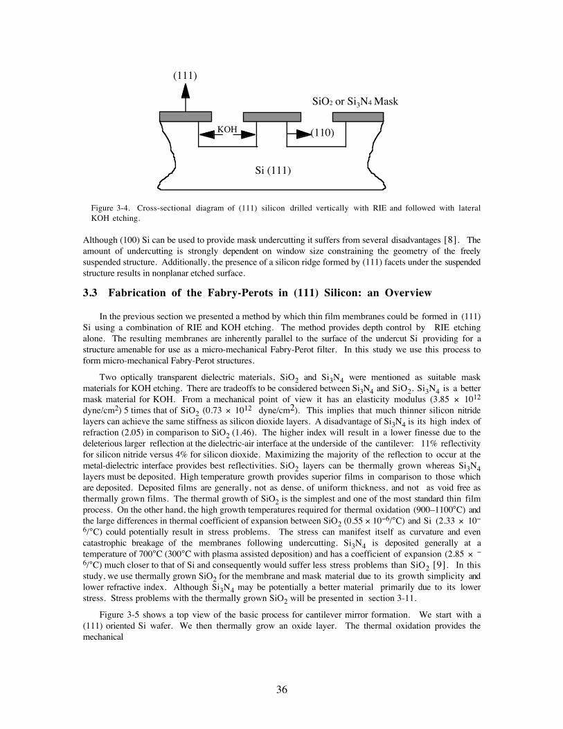
36
Si (111)
SiO2 or Si3N4 Mask
(110)KOH
(111)
Figure 3-4. Cross-sectional diagram of (111) silicon drilled vertically with RIE and followed with lateralKOH etching.
Although (100) Si can be used to provide mask undercutting it suffers from several disadvantages [8]. Theamount of undercutting is strongly dependent on window size constraining the geometry of the freelysuspended structure. Additionally, the presence of a silicon ridge formed by (111) facets under the suspendedstructure results in nonplanar etched surface.
3.3 Fabrication of the Fabry-Perots in (111) Silicon: an Overview
In the previous section we presented a method by which thin film membranes could be formed in (111)Si using a combination of RIE and KOH etching. The method provides depth control by RIE etchingalone. The resulting membranes are inherently parallel to the surface of the undercut Si providing for astructure amenable for use as a micro-mechanical Fabry-Perot filter. In this study we use this process toform micro-mechanical Fabry-Perot structures.
Two optically transparent dielectric materials, SiO2 and Si3N4 were mentioned as suitable maskmaterials for KOH etching. There are tradeoffs to be considered between Si3N4 and SiO2. Si3N4 is a bettermask material for KOH. From a mechanical point of view it has an elasticity modulus (3.85 ´ 1012
dyne/cm2) 5 times that of SiO2 (0.73 ´ 1012 dyne/cm2). This implies that much thinner silicon nitridelayers can achieve the same stiffness as silicon dioxide layers. A disadvantage of Si3N4 is its high index ofrefraction (2.05) in comparison to SiO2 (1.46). The higher index will result in a lower finesse due to thedeleterious larger reflection at the dielectric-air interface at the underside of the cantilever: 11% reflectivityfor silicon nitride versus 4% for silicon dioxide. Maximizing the majority of the reflection to occur at themetal-dielectric interface provides best reflectivities. SiO2 layers can be thermally grown whereas Si3N4layers must be deposited. High temperature growth provides superior films in comparison to those whichare deposited. Deposited films are generally, not as dense, of uniform thickness, and not as void free asthermally grown films. The thermal growth of SiO2 is the simplest and one of the most standard thin filmprocess. On the other hand, the high growth temperatures required for thermal oxidation (900Ð1100°C) andthe large differences in thermal coefficient of expansion between SiO2 (0.55 ´ 10-6/°C) and Si (2.33 ´ 10-
6/°C) could potentially result in stress problems. The stress can manifest itself as curvature and evencatastrophic breakage of the membranes following undercutting. Si3N4 is deposited generally at atemperature of 700°C (300°C with plasma assisted deposition) and has a coefficient of expansion (2.85 ´ -
6/°C) much closer to that of Si and consequently would suffer less stress problems than SiO2 [9]. In thisstudy, we use thermally grown SiO2 for the membrane and mask material due to its growth simplicity andlower refractive index. Although Si3N4 may be potentially a better material primarily due to its lowerstress. Stress problems with the thermally grown SiO2 will be presented in section 3-11.
Figure 3-5 shows a top view of the basic process for cantilever mirror formation. We start with a(111) oriented Si wafer. We then thermally grow an oxide layer. The thermal oxidation provides themechanical
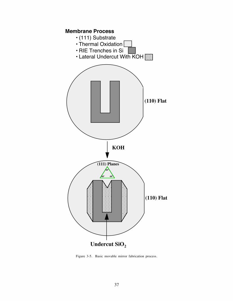
37
(111) Planes60¡
60¡ 60¡
(110) Flat
Undercut SiO2
Membrane Process¥ (111) Substrate¥ Thermal Oxidation¥ RIE Trenches in Si¥ Lateral Undercut With KOH
KOH
(110) Flat
Figure 3-5. Basic movable mirror fabrication process.
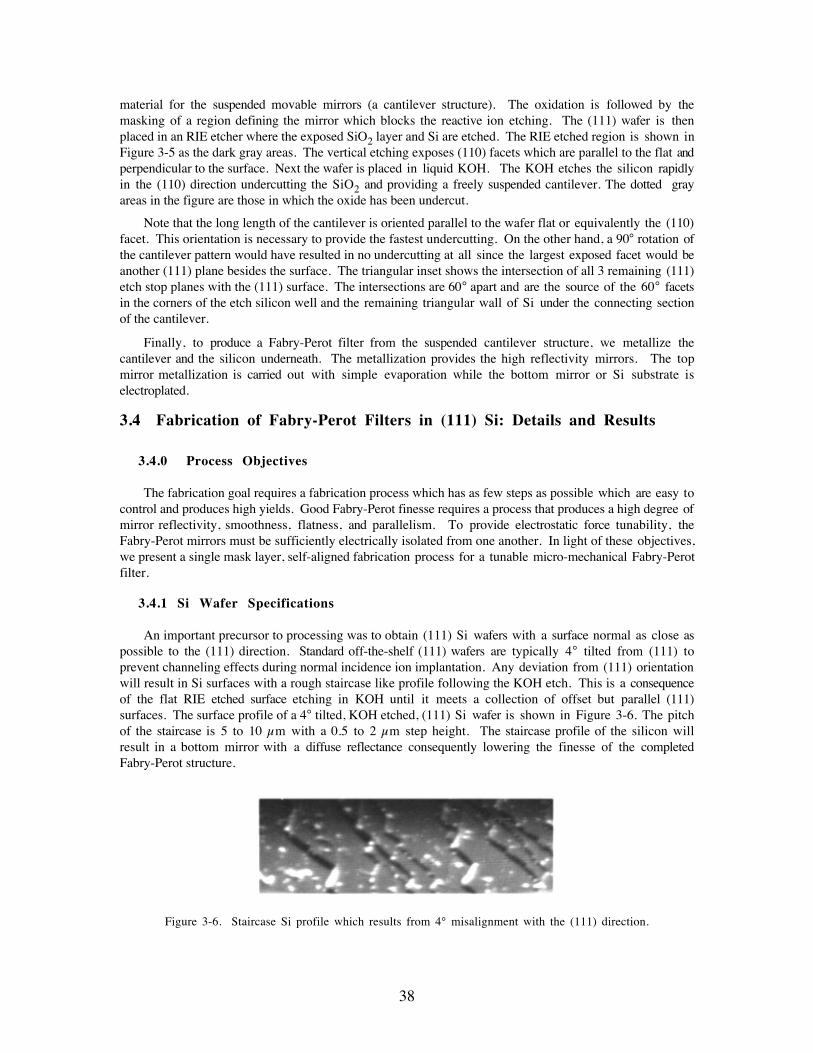
38
material for the suspended movable mirrors (a cantilever structure). The oxidation is followed by themasking of a region defining the mirror which blocks the reactive ion etching. The (111) wafer is thenplaced in an RIE etcher where the exposed SiO2 layer and Si are etched. The RIE etched region is shown inFigure 3-5 as the dark gray areas. The vertical etching exposes (110) facets which are parallel to the flat andperpendicular to the surface. Next the wafer is placed in liquid KOH. The KOH etches the silicon rapidlyin the (110) direction undercutting the SiO2 and providing a freely suspended cantilever. The dotted grayareas in the figure are those in which the oxide has been undercut.
Note that the long length of the cantilever is oriented parallel to the wafer flat or equivalently the (110)facet. This orientation is necessary to provide the fastest undercutting. On the other hand, a 90° rotation ofthe cantilever pattern would have resulted in no undercutting at all since the largest exposed facet would beanother (111) plane besides the surface. The triangular inset shows the intersection of all 3 remaining (111)etch stop planes with the (111) surface. The intersections are 60° apart and are the source of the 60° facetsin the corners of the etch silicon well and the remaining triangular wall of Si under the connecting sectionof the cantilever.
Finally, to produce a Fabry-Perot filter from the suspended cantilever structure, we metallize thecantilever and the silicon underneath. The metallization provides the high reflectivity mirrors. The topmirror metallization is carried out with simple evaporation while the bottom mirror or Si substrate iselectroplated.
3.4 Fabrication of Fabry-Perot Filters in (111) Si: Details and Results
3.4.0 Process Objectives
The fabrication goal requires a fabrication process which has as few steps as possible which are easy tocontrol and produces high yields. Good Fabry-Perot finesse requires a process that produces a high degree ofmirror reflectivity, smoothness, flatness, and parallelism. To provide electrostatic force tunability, theFabry-Perot mirrors must be sufficiently electrically isolated from one another. In light of these objectives,we present a single mask layer, self-aligned fabrication process for a tunable micro-mechanical Fabry-Perotfilter.
3.4.1 Si Wafer Specifications
An important precursor to processing was to obtain (111) Si wafers with a surface normal as close aspossible to the (111) direction. Standard off-the-shelf (111) wafers are typically 4° tilted from (111) toprevent channeling effects during normal incidence ion implantation. Any deviation from (111) orientationwill result in Si surfaces with a rough staircase like profile following the KOH etch. This is a consequenceof the flat RIE etched surface etching in KOH until it meets a collection of offset but parallel (111)surfaces. The surface profile of a 4° tilted, KOH etched, (111) Si wafer is shown in Figure 3-6. The pitchof the staircase is 5 to 10 µm with a 0.5 to 2 µm step height. The staircase profile of the silicon willresult in a bottom mirror with a diffuse reflectance consequently lowering the finesse of the completedFabry-Perot structure.
Figure 3-6. Staircase Si profile which results from 4¡ misalignment with the (111) direction.
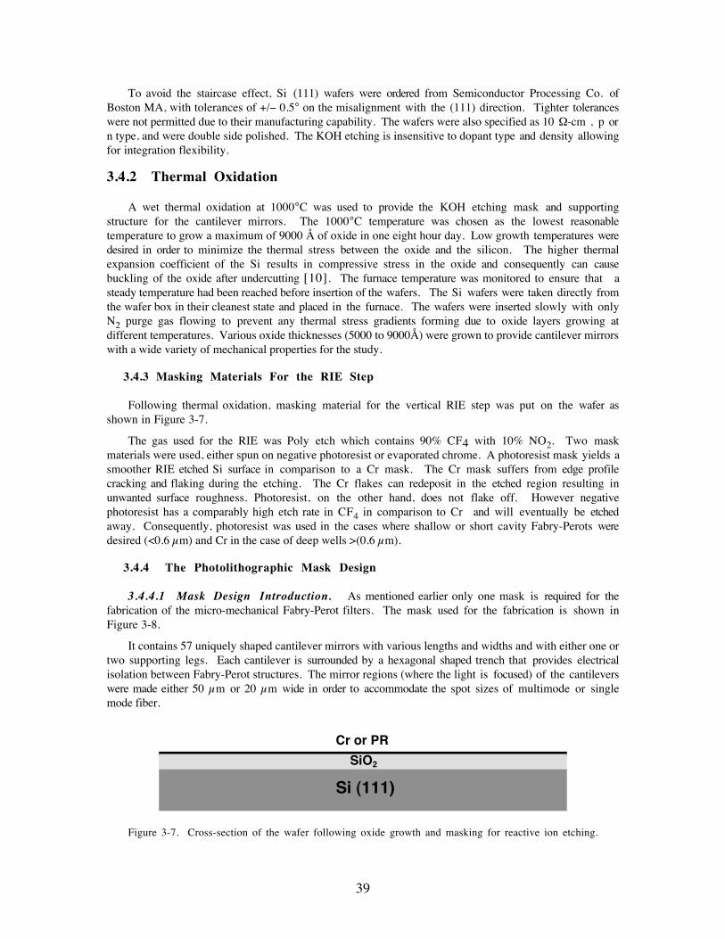
39
To avoid the staircase effect, Si (111) wafers were ordered from Semiconductor Processing Co. ofBoston MA, with tolerances of +/- 0.5° on the misalignment with the (111) direction. Tighter toleranceswere not permitted due to their manufacturing capability. The wafers were also specified as 10 ½-cm , p orn type, and were double side polished. The KOH etching is insensitive to dopant type and density allowingfor integration flexibility.
3.4.2 Thermal Oxidation
A wet thermal oxidation at 1000°C was used to provide the KOH etching mask and supportingstructure for the cantilever mirrors. The 1000°C temperature was chosen as the lowest reasonabletemperature to grow a maximum of 9000 � of oxide in one eight hour day. Low growth temperatures weredesired in order to minimize the thermal stress between the oxide and the silicon. The higher thermalexpansion coefficient of the Si results in compressive stress in the oxide and consequently can causebuckling of the oxide after undercutting [10]. The furnace temperature was monitored to ensure that asteady temperature had been reached before insertion of the wafers. The Si wafers were taken directly fromthe wafer box in their cleanest state and placed in the furnace. The wafers were inserted slowly with onlyN2 purge gas flowing to prevent any thermal stress gradients forming due to oxide layers growing atdifferent temperatures. Various oxide thicknesses (5000 to 9000�) were grown to provide cantilever mirrorswith a wide variety of mechanical properties for the study.
3.4.3 Masking Materials For the RIE Step
Following thermal oxidation, masking material for the vertical RIE step was put on the wafer asshown in Figure 3-7.
The gas used for the RIE was Poly etch which contains 90% CF4 with 10% NO2. Two maskmaterials were used, either spun on negative photoresist or evaporated chrome. A photoresist mask yields asmoother RIE etched Si surface in comparison to a Cr mask. The Cr mask suffers from edge profilecracking and flaking during the etching. The Cr flakes can redeposit in the etched region resulting inunwanted surface roughness. Photoresist, on the other hand, does not flake off. However negativephotoresist has a comparably high etch rate in CF4 in comparison to Cr and will eventually be etchedaway. Consequently, photoresist was used in the cases where shallow or short cavity Fabry-Perots weredesired (<0.6 µm) and Cr in the case of deep wells >(0.6 µm).
3.4.4 The Photolithographic Mask Design
3.4.4.1 Mask Design Introduction. As mentioned earlier only one mask is required for thefabrication of the micro-mechanical Fabry-Perot filters. The mask used for the fabrication is shown inFigure 3-8.
It contains 57 uniquely shaped cantilever mirrors with various lengths and widths and with either one ortwo supporting legs. Each cantilever is surrounded by a hexagonal shaped trench that provides electricalisolation between Fabry-Perot structures. The mirror regions (where the light is focused) of the cantileverswere made either 50 µm or 20 µm wide in order to accommodate the spot sizes of multimode or singlemode fiber.
Si (111)
SiO2
Cr or PR
Figure 3-7. Cross-section of the wafer following oxide growth and masking for reactive ion etching.
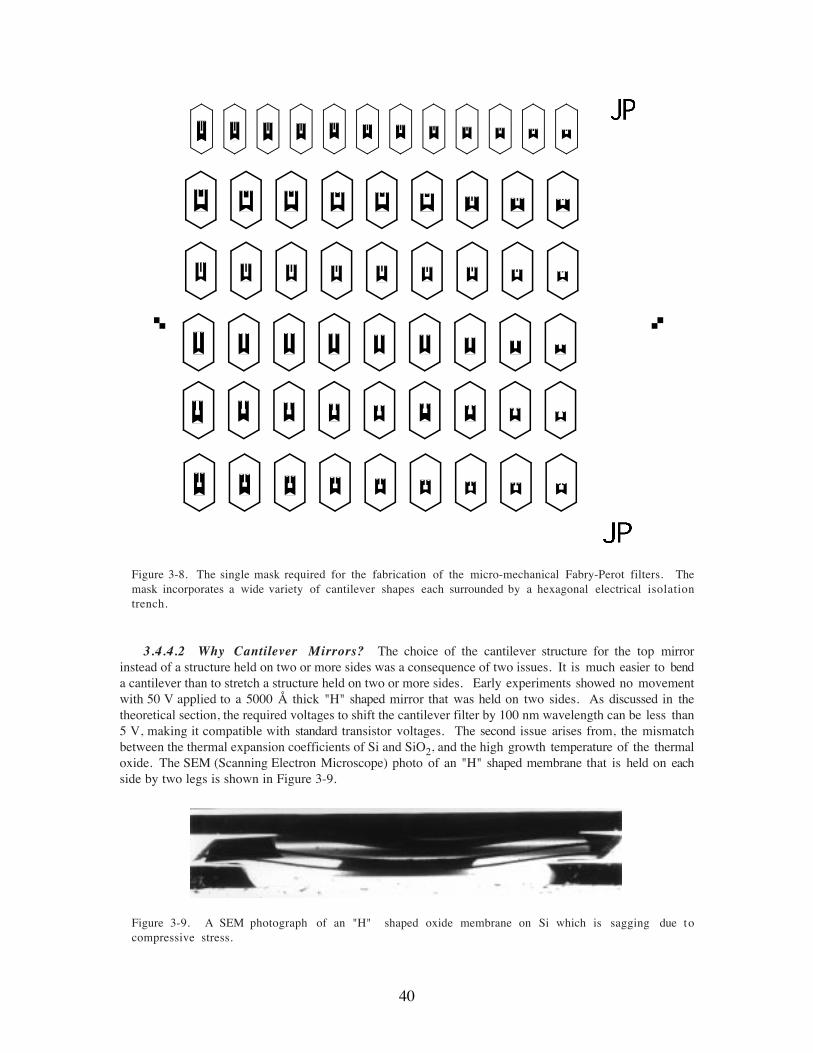
40
Figure 3-8. The single mask required for the fabrication of the micro-mechanical Fabry-Perot filters. Themask incorporates a wide variety of cantilever shapes each surrounded by a hexagonal electrical isolationtrench.
3.4.4.2 Why Cantilever Mirrors? The choice of the cantilever structure for the top mirrorinstead of a structure held on two or more sides was a consequence of two issues. It is much easier to benda cantilever than to stretch a structure held on two or more sides. Early experiments showed no movementwith 50 V applied to a 5000 � thick "H" shaped mirror that was held on two sides. As discussed in thetheoretical section, the required voltages to shift the cantilever filter by 100 nm wavelength can be less than5 V, making it compatible with standard transistor voltages. The second issue arises from, the mismatchbetween the thermal expansion coefficients of Si and SiO2, and the high growth temperature of the thermaloxide. The SEM (Scanning Electron Microscope) photo of an "H" shaped membrane that is held on eachside by two legs is shown in Figure 3-9.
Figure 3-9. A SEM photograph of an "H" shaped oxide membrane on Si which is sagging due tocompressive stress.

41
This cantilever is 150 µm long and exhibits a sag of 5.5 µm in a 7 µm deep Si well. The sag is aconsequence of the much higher coefficient of thermal expansion of Si in comparison to SiO2 and the highgrowth temperature of the SiO2. The oxide was grown at 1000¡C temperature, with aSi = 2.6 ´ 10-6/°Cand aSiO2 = 5 ´ 10-7/°C. As the membrane structures cool to room temperature following removal fromthe furnace, the Si substrate contracts five times more than the SiO2 placing it under compression.Following the removal of the Si underneath the membrane it relaxes through expansion and sags. The sagproduces a central mirror area which is not optimally flat. Instead it is concave up which results in anunstable optical resonator. One solution to this problem is to use deposited low temperature oxide, siliconnitride, or silicon oxynitride for the membrane material. These films can be deposited on silicon with muchlower stress.
Cantilevers, on the other hand, do not suffer from the sagging problem even with large thermalcoefficient of expansion differences. Instead, as the silicon underneath the oxide cantilever is removed, it isallowed to freely expand at the free end without buckling. As a consequence of the bending ease and reducedthermal oxide buckling, the study focused on the cantilever mirror structure.
3.4.4.3 Mask Design For Electrical Isolation. The top mirrors or cantilevers must beelectrically isolated from the bottom mirror to provide voltage tunability. A capacitive charging of themirrors provides the electrostatic bending force on the cantilever. Furthermore, each of the Fabry-Perotcantilever mirrors on the die must be electrically isolated from one another to provide for independentvoltage tuning.
One mask is used to provide for both the undercutting of the cantilevers and the electrical isolation.We provide the electrical isolation by using the same undercutting technique as used for the removal of thesilicon underneath the cantilever. The method relies on undercut oxide eaves as a means to create anelectrical discontinuity between, the top and bottom mirror of each device and between top mirrors in thearray. The electrical discontinuity occurs at the underside of the electrically insulating oxide eave. Theunderside of the eave is left uncoated during the top and bottom mirror metallization.
As discussed earlier there are three other slowly etching (111) planes besides the surface normal. Theirintersections with the surface normal create an equilateral triangle with one side perpendicular to the waferflat. To provide undercut oxide eaves by KOH etching, we avoid exposing the additional (111) facets duringthe RIE etch step.
Electrical isolation between the cantilever or top mirror and the silicon region below can be achieved byetching a well with the RIE which has two outside walls parallel to the flat on the two opposite sides of thecantilever as shown in Figure 3-10. The Si facet for these sides are the fast etching (110) planes whicheasily provide an oxide eave after KOH etching. On the sides perpendicular to the line of the flat we mustuse a more complex wall shape to ensure the presence of an undercut eave following the KOH step. Thiswall if made simply perpendicular to the flat would be opening on a slowly etching (111) facet so that verylittle undercutting would occur. However, if the wall is shaped with an opening oriented midway betweentwo (111) facets, undercutting will result. This was done with a 30°Ð30°Ð120° triangle wall shape asshown in Figure 3-10.
To electrically isolate the top mirrors of different Fabry-Perot devices from each other, the same methodis used. A hexagonal shaped isolation trench is etched around the entire structure with sides oriented foroptimal undercutting of oxide eaves. The trench has two sides parallel to the fast undercutting (110) flatwith the same 30°Ð30°Ð120° triangle capping them as shown in Figure 3-10.
3.4.5 Reactive Ion Etching of the Si Well and Isolation Trench
Following the application of the photoresist or chromium masking layer, the layer isphotolithographically patterned resulting in the cross section shown in Figure 3-11. The gas used for theRIE was Poly etch which contains CF4 diluted with 10% NO2 .
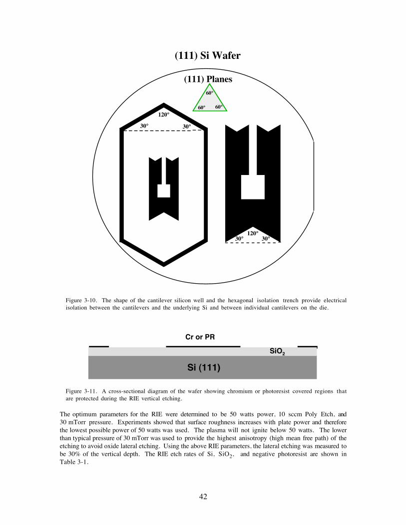
42
30¡ 30¡
120¡
(111) Si Wafer
60¡
60¡ 60¡
(111) Planes
30¡ 30¡120¡
Figure 3-10. The shape of the cantilever silicon well and the hexagonal isolation trench provide electricalisolation between the cantilevers and the underlying Si and between individual cantilevers on the die.
Cr or PR
SiO2
Si (111)
Figure 3-11. A cross-sectional diagram of the wafer showing chromium or photoresist covered regions thatare protected during the RIE vertical etching.
The optimum parameters for the RIE were determined to be 50 watts power, 10 sccm Poly Etch, and30ÊmTorr pressure. Experiments showed that surface roughness increases with plate power and thereforethe lowest possible power of 50 watts was used. The plasma will not ignite below 50 watts. The lowerthan typical pressure of 30 mTorr was used to provide the highest anisotropy (high mean free path) of theetching to avoid oxide lateral etching. Using the above RIE parameters, the lateral etching was measured tobe 30% of the vertical depth. The RIE etch rates of Si, SiO2, and negative photoresist are shown inTableÊ3-1.
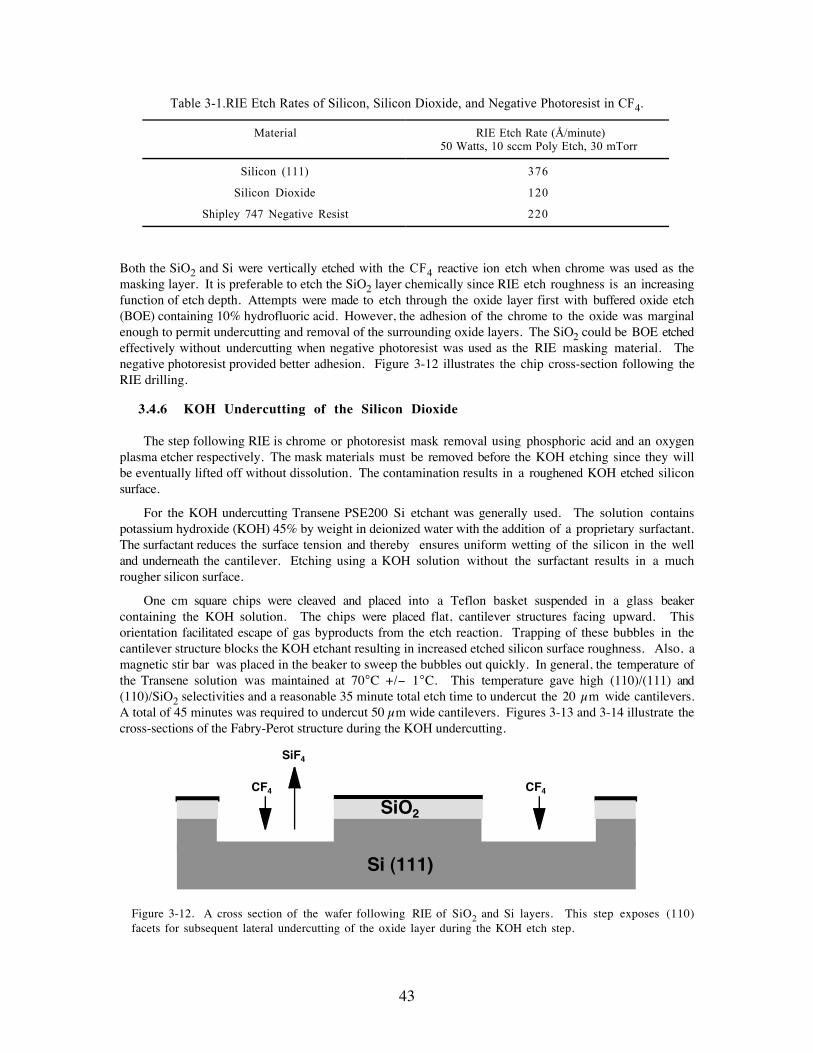
43
Table 3-1.RIE Etch Rates of Silicon, Silicon Dioxide, and Negative Photoresist in CF4.
Material RIE Etch Rate (�/minute)50 Watts, 10 sccm Poly Etch, 30 mTorr
Silicon (111) 376
Silicon Dioxide 120
Shipley 747 Negative Resist 220
Both the SiO2 and Si were vertically etched with the CF4 reactive ion etch when chrome was used as themasking layer. It is preferable to etch the SiO2 layer chemically since RIE etch roughness is an increasingfunction of etch depth. Attempts were made to etch through the oxide layer first with buffered oxide etch(BOE) containing 10% hydrofluoric acid. However, the adhesion of the chrome to the oxide was marginalenough to permit undercutting and removal of the surrounding oxide layers. The SiO2 could be BOE etchedeffectively without undercutting when negative photoresist was used as the RIE masking material. Thenegative photoresist provided better adhesion. Figure 3-12 illustrates the chip cross-section following theRIE drilling.
3.4.6 KOH Undercutting of the Silicon Dioxide
The step following RIE is chrome or photoresist mask removal using phosphoric acid and an oxygenplasma etcher respectively. The mask materials must be removed before the KOH etching since they willbe eventually lifted off without dissolution. The contamination results in a roughened KOH etched siliconsurface.
For the KOH undercutting Transene PSE200 Si etchant was generally used. The solution containspotassium hydroxide (KOH) 45% by weight in deionized water with the addition of a proprietary surfactant.The surfactant reduces the surface tension and thereby ensures uniform wetting of the silicon in the welland underneath the cantilever. Etching using a KOH solution without the surfactant results in a muchrougher silicon surface.
One cm square chips were cleaved and placed into a Teflon basket suspended in a glass beakercontaining the KOH solution. The chips were placed flat, cantilever structures facing upward. Thisorientation facilitated escape of gas byproducts from the etch reaction. Trapping of these bubbles in thecantilever structure blocks the KOH etchant resulting in increased etched silicon surface roughness. Also, amagnetic stir bar was placed in the beaker to sweep the bubbles out quickly. In general, the temperature ofthe Transene solution was maintained at 70°C +/- 1°C. This temperature gave high (110)/(111) and(110)/SiO2 selectivities and a reasonable 35 minute total etch time to undercut the 20 µm wide cantilevers.A total of 45 minutes was required to undercut 50 µm wide cantilevers. Figures 3-13 and 3-14 illustrate thecross-sections of the Fabry-Perot structure during the KOH undercutting.
Si Substrate
CF4
Si (111)
SiO2
CF4
SiF4
Figure 3-12. A cross section of the wafer following RIE of SiO2 and Si layers. This step exposes (110)facets for subsequent lateral undercutting of the oxide layer during the KOH etch step.
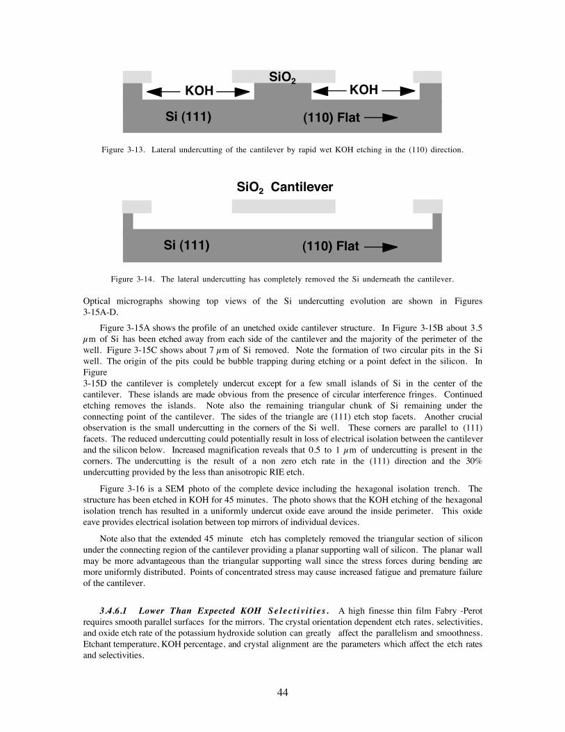
44
Si Substrate
KOH KOH
(110) Flat
SiO2
Si (111)
Figure 3-13. Lateral undercutting of the cantilever by rapid wet KOH etching in the (110) direction.
Si Substrate(110) Flat
SiO2 Cantilever
Si (111)
Figure 3-14. The lateral undercutting has completely removed the Si underneath the cantilever.
Optical micrographs showing top views of the Si undercutting evolution are shown in Figures3-15A-D.
Figure 3-15A shows the profile of an unetched oxide cantilever structure. In Figure 3-15B about 3.5µm of Si has been etched away from each side of the cantilever and the majority of the perimeter of thewell. Figure 3-15C shows about 7 µm of Si removed. Note the formation of two circular pits in the Siwell. The origin of the pits could be bubble trapping during etching or a point defect in the silicon. InFigure3-15D the cantilever is completely undercut except for a few small islands of Si in the center of thecantilever. These islands are made obvious from the presence of circular interference fringes. Continuedetching removes the islands. Note also the remaining triangular chunk of Si remaining under theconnecting point of the cantilever. The sides of the triangle are (111) etch stop facets. Another crucialobservation is the small undercutting in the corners of the Si well. These corners are parallel to (111)facets. The reduced undercutting could potentially result in loss of electrical isolation between the cantileverand the silicon below. Increased magnification reveals that 0.5 to 1 µm of undercutting is present in thecorners. The undercutting is the result of a non zero etch rate in the (111) direction and the 30%undercutting provided by the less than anisotropic RIE etch.
Figure 3-16 is a SEM photo of the complete device including the hexagonal isolation trench. Thestructure has been etched in KOH for 45 minutes. The photo shows that the KOH etching of the hexagonalisolation trench has resulted in a uniformly undercut oxide eave around the inside perimeter. This oxideeave provides electrical isolation between top mirrors of individual devices.
Note also that the extended 45 minute etch has completely removed the triangular section of siliconunder the connecting region of the cantilever providing a planar supporting wall of silicon. The planar wallmay be more advantageous than the triangular supporting wall since the stress forces during bending aremore uniformly distributed. Points of concentrated stress may cause increased fatigue and premature failureof the cantilever.
3.4.6.1 Lower Than Expected KOH Se lec t i v i t i e s . A high finesse thin film Fabry -Perotrequires smooth parallel surfaces for the mirrors. The crystal orientation dependent etch rates, selectivities,and oxide etch rate of the potassium hydroxide solution can greatly affect the parallelism and smoothness. Etchant temperature, KOH percentage, and crystal alignment are the parameters which affect the etch ratesand selectivities.
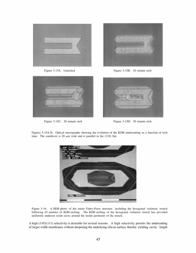
45
Figure 3-15A. Unetched Figure 3-15B. 10 minute etch
Figure 3-15C. 20 minute etch Figure 3-15D. 30 minute etch
Figures 3-15A-D. Optical micrographs showing the evolution of the KOH undercutting as a function of etchtime. The cantilever is 20 µm wide and is parallel to the (110) flat.
Figure 3-16. A SEM photo of the entire Fabry-Perot structure including the hexagonal isolation trenchfollowing 45 minutes of KOH etching. The KOH etching of the hexagonal isolation trench has provideduniformly undercut oxide eaves around the inside perimeter of the trench.
A high (110)/(111) selectivity is desirable for several reasons. A high selectivity permits the undercuttingof larger width membranes without deepening the underlying silicon surface thereby yielding cavity length
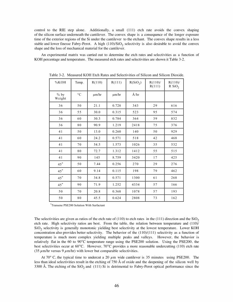
46
control to the RIE step alone. Additionally, a small (111) etch rate avoids the convex shapingof the silicon surface underneath the cantilever. The convex shape is a consequence of the longer exposuretime of the exterior regions of the Si under the cantilever to the etchant. The convex shape results in a lessstable and lower finesse Fabry-Perot. A high (110)/SiO2 selectivity is also desirable to avoid the convexshape and the loss of mechanical material for the cantilever.
An experimental matrix was carried out to determine the etch rates and selectivities as a function ofKOH percentage and temperature. The measured etch rates and selectivities are shown it Table 3-2.
Table 3-2. Measured KOH Etch Rates and Selectivities of Silicon and Silicon Dioxide.
%KOH Temp. R(110) R(111) R(SiO2) R(110)/R(111)
R(110)/R SiO2
% byWeight
¡C µm/hr µm/hr �/hr
36 50 21.1 0.728 343 29 616
36 55 30.0 0.315 523 95 574
36 60 30.3 0.784 364 39 832
36 80 90.9 1.219 2418 75 376
41 50 13.0 0.260 140 50 929
41 60 24.2 0.571 518 42 468
41 70 54.5 1.573 1026 35 532
41 80 72.7 1.312 1412 55 515
41 90 145 8.759 3420 17 425
45* 50 7.44 0.256 270 29 276
45* 60 9.14 0.115 198 79 462
45* 70 34.8 0.571 1300 61 268
45* 90 71.9 1.252 4334 57 166
50 70 20.8 0.368 1078 57 193
50 80 45.5 0.624 2808 73 162
*Transene PSE200 Solution With Surfactant
The selectivities are given as ratios of the etch rate of (110) to etch rates in the (111) direction and the SiO2etch rate. High selectivity ratios are best. From the table, the relation between temperature and (110)/SiO2 selectivity is generally monotonic yielding best selectivity at the lowest temperature. Lower KOHconcentration also provides better selectivity. The behavior of the (110)/(111) selectivity as a function oftemperature is much more complex yielding multiple peaks and valleys. However, the behavior isrelatively flat in the 60 to 90°C temperature range using the PSE200 solution. Using the PSE200, thebest selectivities occur at 60°C. However, 70°C provides a more reasonable undercutting (110) etch rate(35ʵm/hr versus 9 µm/hr) with lower but comparable selectivities.
At 70¡ C, the typical time to undercut a 20 µm wide cantilever is 35 minutes using PSE200. Theless than ideal selectivities result in the etching of 750 � of oxide and the deepening of the silicon well by3300 �. The etching of the SiO2 and (111) Si is detrimental to Fabry-Perot optical performance since the
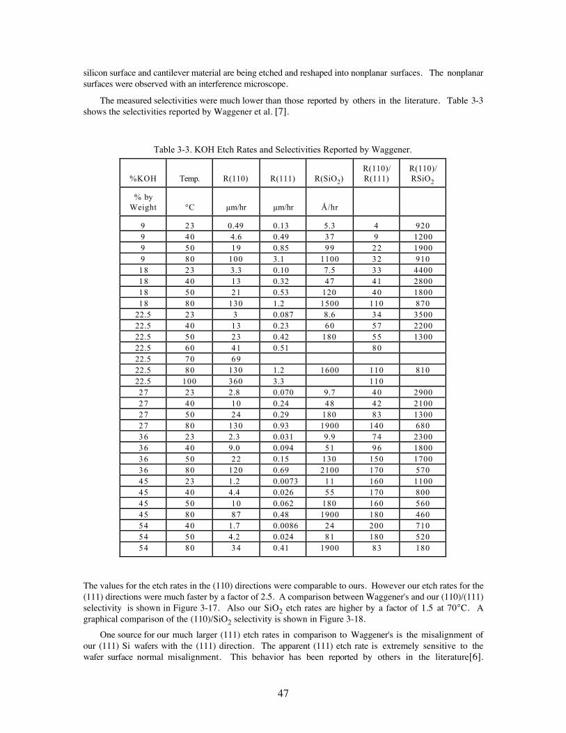
47
silicon surface and cantilever material are being etched and reshaped into nonplanar surfaces. The nonplanarsurfaces were observed with an interference microscope.
The measured selectivities were much lower than those reported by others in the literature. Table 3-3shows the selectivities reported by Waggener et al. [7].
Table 3-3. KOH Etch Rates and Selectivities Reported by Waggener.
%KOH Temp. R(110) R(111) R(SiO2)R(110)/R(111)
R(110)/RSiO2
% byWeight ¡C µm/hr µm/hr �/hr
9 23 0.49 0.13 5.3 4 9209 40 4.6 0.49 37 9 12009 50 19 0.85 99 22 19009 80 100 3.1 1100 32 91018 23 3.3 0.10 7.5 33 440018 40 13 0.32 47 41 280018 50 21 0.53 120 40 180018 80 130 1.2 1500 110 870
22.5 23 3 0.087 8.6 34 350022.5 40 13 0.23 60 57 220022.5 50 23 0.42 180 55 130022.5 60 41 0.51 8022.5 70 6922.5 80 130 1.2 1600 110 81022.5 100 360 3.3 11027 23 2.8 0.070 9.7 40 290027 40 10 0.24 48 42 210027 50 24 0.29 180 83 130027 80 130 0.93 1900 140 68036 23 2.3 0.031 9.9 74 230036 40 9.0 0.094 51 96 180036 50 22 0.15 130 150 170036 80 120 0.69 2100 170 57045 23 1.2 0.0073 11 160 110045 40 4.4 0.026 55 170 80045 50 10 0.062 180 160 56045 80 87 0.48 1900 180 46054 40 1.7 0.0086 24 200 71054 50 4.2 0.024 81 180 52054 80 34 0.41 1900 83 180
The values for the etch rates in the (110) directions were comparable to ours. However our etch rates for the(111) directions were much faster by a factor of 2.5. A comparison between Waggener's and our (110)/(111)selectivity is shown in Figure 3-17. Also our SiO2 etch rates are higher by a factor of 1.5 at 70°C. Agraphical comparison of the (110)/SiO2 selectivity is shown in Figure 3-18.
One source for our much larger (111) etch rates in comparison to Waggener's is the misalignment ofour (111) Si wafers with the (111) direction. The apparent (111) etch rate is extremely sensitive to thewafer surface normal misalignment. This behavior has been reported by others in the literature[6].
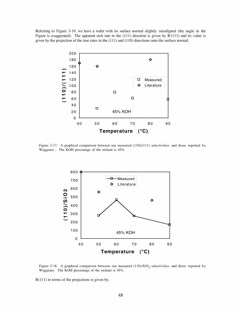
48
Referring to Figure 3-19, we have a wafer with its surface normal slightly misaligned (the angle in theFigure is exaggerated). The apparent etch rate in the (111) direction is given by R'(111) and its value isgiven by the projection of the true rates in the (111) and (110) directions onto the surface normal.
0
2 0
4 0
6 0
8 0
100
120
140
160
180
200
4 0 5 0 6 0 7 0 8 0 9 0
Temperature (¡C)
(11
0)/
(11
1)
Measured
Literature
45% KOH
Figure 3-17. A graphical comparison between our measured (110)/(111) selectivities and those reported byWaggener . The KOH percentage of the etchant is 45%.
0
100
200
300
400
500
600
700
800
4 0 5 0 6 0 7 0 8 0 9 0
Temperature (¡C)
(11
0)/
SiO
2
Measured
Literature
45% KOH
Figure 3-18. A graphical comparison between our measured (110)/SiO2 selectivities and those reported byWaggener. The KOH percentage of the etchant is 45%.
R(111) in terms of the projections is given by:
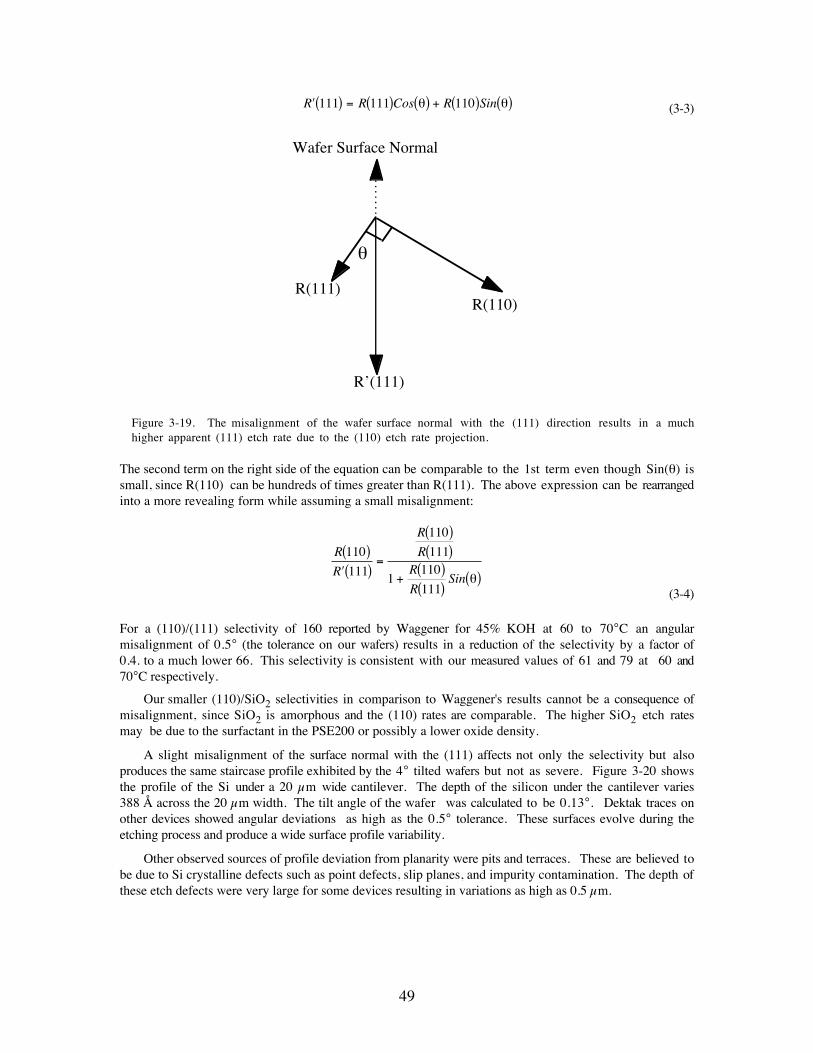
49
¢( ) = ( ) ( ) + ( ) ( )R R Cos R Sin111 111 110q q (3-3)
Wafer Surface Normal
R(110)R(111)
RÕ(111)
q
Figure 3-19. The misalignment of the wafer surface normal with the (111) direction results in a muchhigher apparent (111) etch rate due to the (110) etch rate projection.
The second term on the right side of the equation can be comparable to the 1st term even though Sin(q) issmall, since R(110) can be hundreds of times greater than R(111). The above expression can be rearrangedinto a more revealing form while assuming a small misalignment:
R
R
R
RR
RSin
110
111
110
111
1110
111
( )¢( )
=
( )( )
+( )( )
( )q(3-4)
For a (110)/(111) selectivity of 160 reported by Waggener for 45% KOH at 60 to 70°C an angularmisalignment of 0.5° (the tolerance on our wafers) results in a reduction of the selectivity by a factor of0.4. to a much lower 66. This selectivity is consistent with our measured values of 61 and 79 at 60 and70°C respectively.
Our smaller (110)/SiO2 selectivities in comparison to Waggener's results cannot be a consequence ofmisalignment, since SiO2 is amorphous and the (110) rates are comparable. The higher SiO2 etch ratesmay be due to the surfactant in the PSE200 or possibly a lower oxide density.
A slight misalignment of the surface normal with the (111) affects not only the selectivity but alsoproduces the same staircase profile exhibited by the 4° tilted wafers but not as severe. Figure 3-20 showsthe profile of the Si under a 20 µm wide cantilever. The depth of the silicon under the cantilever varies388Ê� across the 20 µm width. The tilt angle of the wafer was calculated to be 0.13°. Dektak traces onother devices showed angular deviations as high as the 0.5° tolerance. These surfaces evolve during theetching process and produce a wide surface profile variability.
Other observed sources of profile deviation from planarity were pits and terraces. These are believed tobe due to Si crystalline defects such as point defects, slip planes, and impurity contamination. The depth ofthese etch defects were very large for some devices resulting in variations as high as 0.5 µm.
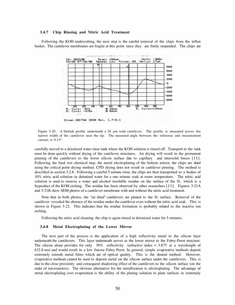
50
3.4.7 Chip Rinsing and Nitric Acid Treatment
Following the KOH undercutting, the next step is the careful removal of the chips from the teflonbasket. The cantilever membranes are fragile at this point since they are freely suspended. The chips are
Figure 3-20. A Dektak profile underneath a 20 µm wide cantilever. The profile is measured across thenarrow width of the cantilever near the tip. The measured angle between the reference and measurementcursors is 0.13¡.
carefully moved to a deionized water rinse tank where the KOH solution is rinsed off. Transport to the tankmust be done quickly without drying of the cantilever structures. Air drying will result in the permanentpinning of the cantilevers to the lower silicon surface due to capillary and intersolid forces [11].Following the final wet chemical step, the metal electroplating of the bottom mirror, the chips are driedusing the critical point drying method. CPD drying does not result in cantilever pinning. The method isdescribed in section 3.2.8. Following a careful 5 minute rinse, the chips are then transported to a beaker of10% nitric acid solution in deionized water for a one minute soak at room temperature. The nitric acidsolution is used to remove a water and alcohol insoluble residue on the surface of the Si, which is abyproduct of the KOH etching. The residue has been observed by other researchers [11]. Figures 3-21Aand 3-21B show SEM photos of a cantilever membrane with and without the nitric acid treatment.
Note that in both photos, the "air dried" cantilevers are pinned to the Si surface. Removal of thecantilever revealed the absence of the residue under the cantilever even without the nitric acid soak. This isshown in Figure 3-22. This indicates that the residue formation is probably related to the reactive ionetching.
Following the nitric acid cleaning, the chip is again rinsed in deionized water for 5 minutes.
3.4.8 Metal Electroplating of the Lower Mirror
The next part of the process is the application of a high reflectivity metal to the silicon layerunderneath the cantilevers. This layer underneath serves as the lower mirror to the Fabry-Perot structure.The silicon alone provides for only 30% reflectivity (refractive index = 3.875 at a wavelength of632.8Ênm) and would result in a low finesse Fabry-Perot. In general, simple evaporative methods depositextremely smooth metal films which are of optical quality. This is the desired method. However,evaporative methods cannot be used to deposit metal on the silicon surface under the cantilevers. This isdue to the close proximity and consequent shadowing effect of the cantilevers to the silicon surface (on theorder of micrometers). The obvious alternative for the metallization is electroplating. The advantage ofmetal electroplating over evaporation is the ability of the plating solution to plate surfaces in extremely
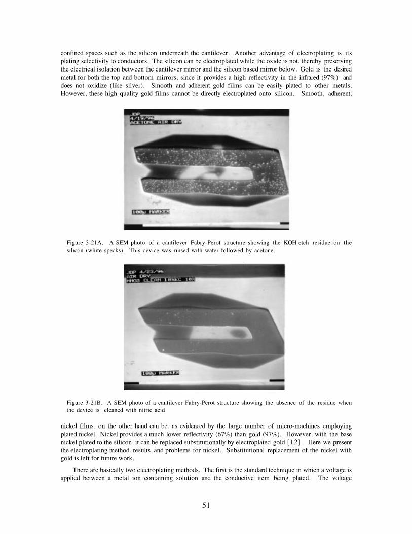
51
confined spaces such as the silicon underneath the cantilever. Another advantage of electroplating is itsplating selectivity to conductors. The silicon can be electroplated while the oxide is not, thereby preservingthe electrical isolation between the cantilever mirror and the silicon based mirror below. Gold is the desiredmetal for both the top and bottom mirrors, since it provides a high reflectivity in the infrared (97%) anddoes not oxidize (like silver). Smooth and adherent gold films can be easily plated to other metals.However, these high quality gold films cannot be directly electroplated onto silicon. Smooth, adherent,
Figure 3-21A. A SEM photo of a cantilever Fabry-Perot structure showing the KOH etch residue on thesilicon (white specks). This device was rinsed with water followed by acetone.
Figure 3-21B. A SEM photo of a cantilever Fabry-Perot structure showing the absence of the residue whenthe device is cleaned with nitric acid.
nickel films, on the other hand can be, as evidenced by the large number of micro-machines employingplated nickel. Nickel provides a much lower reflectivity (67%) than gold (97%). However, with the basenickel plated to the silicon, it can be replaced substitutionally by electroplated gold [12]. Here we presentthe electroplating method, results, and problems for nickel. Substitutional replacement of the nickel withgold is left for future work.
There are basically two electroplating methods. The first is the standard technique in which a voltage isapplied between a metal ion containing solution and the conductive item being plated. The voltage
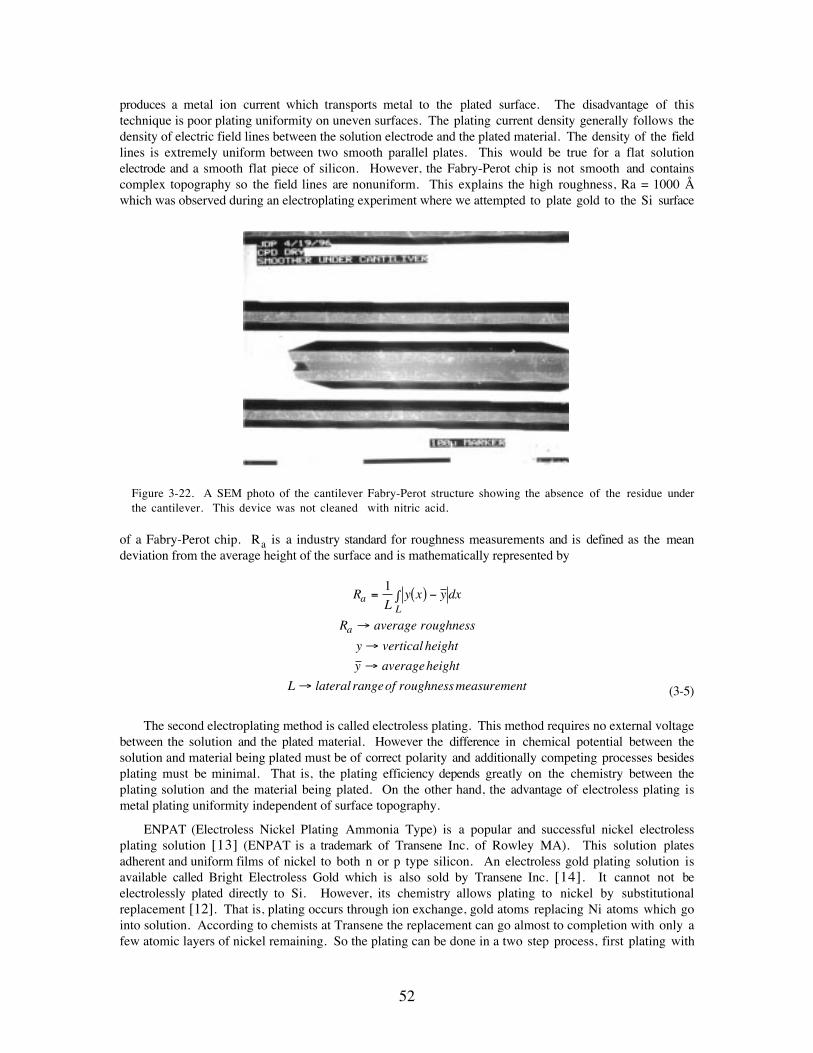
52
produces a metal ion current which transports metal to the plated surface. The disadvantage of thistechnique is poor plating uniformity on uneven surfaces. The plating current density generally follows thedensity of electric field lines between the solution electrode and the plated material. The density of the fieldlines is extremely uniform between two smooth parallel plates. This would be true for a flat solutionelectrode and a smooth flat piece of silicon. However, the Fabry-Perot chip is not smooth and containscomplex topography so the field lines are nonuniform. This explains the high roughness, Ra = 1000 �which was observed during an electroplating experiment where we attempted to plate gold to the Si surface
Figure 3-22. A SEM photo of the cantilever Fabry-Perot structure showing the absence of the residue underthe cantilever. This device was not cleaned with nitric acid.
of a Fabry-Perot chip. Ra is a industry standard for roughness measurements and is defined as the meandeviation from the average height of the surface and is mathematically represented by
RL
y x y dx
R average roughness
y vertical height
y averageheight
L lateral rangeof roughness measurement
aL
a
= ( ) -ò
®
®
®
®
1
(3-5)
The second electroplating method is called electroless plating. This method requires no external voltagebetween the solution and the plated material. However the difference in chemical potential between thesolution and material being plated must be of correct polarity and additionally competing processes besidesplating must be minimal. That is, the plating efficiency depends greatly on the chemistry between theplating solution and the material being plated. On the other hand, the advantage of electroless plating ismetal plating uniformity independent of surface topography.
ENPAT (Electroless Nickel Plating Ammonia Type) is a popular and successful nickel electrolessplating solution [13] (ENPAT is a trademark of Transene Inc. of Rowley MA). This solution platesadherent and uniform films of nickel to both n or p type silicon. An electroless gold plating solution isavailable called Bright Electroless Gold which is also sold by Transene Inc. [14]. It cannot not beelectrolessly plated directly to Si. However, its chemistry allows plating to nickel by substitutionalreplacement [12]. That is, plating occurs through ion exchange, gold atoms replacing Ni atoms which gointo solution. According to chemists at Transene the replacement can go almost to completion with only afew atomic layers of nickel remaining. So the plating can be done in a two step process, first plating with
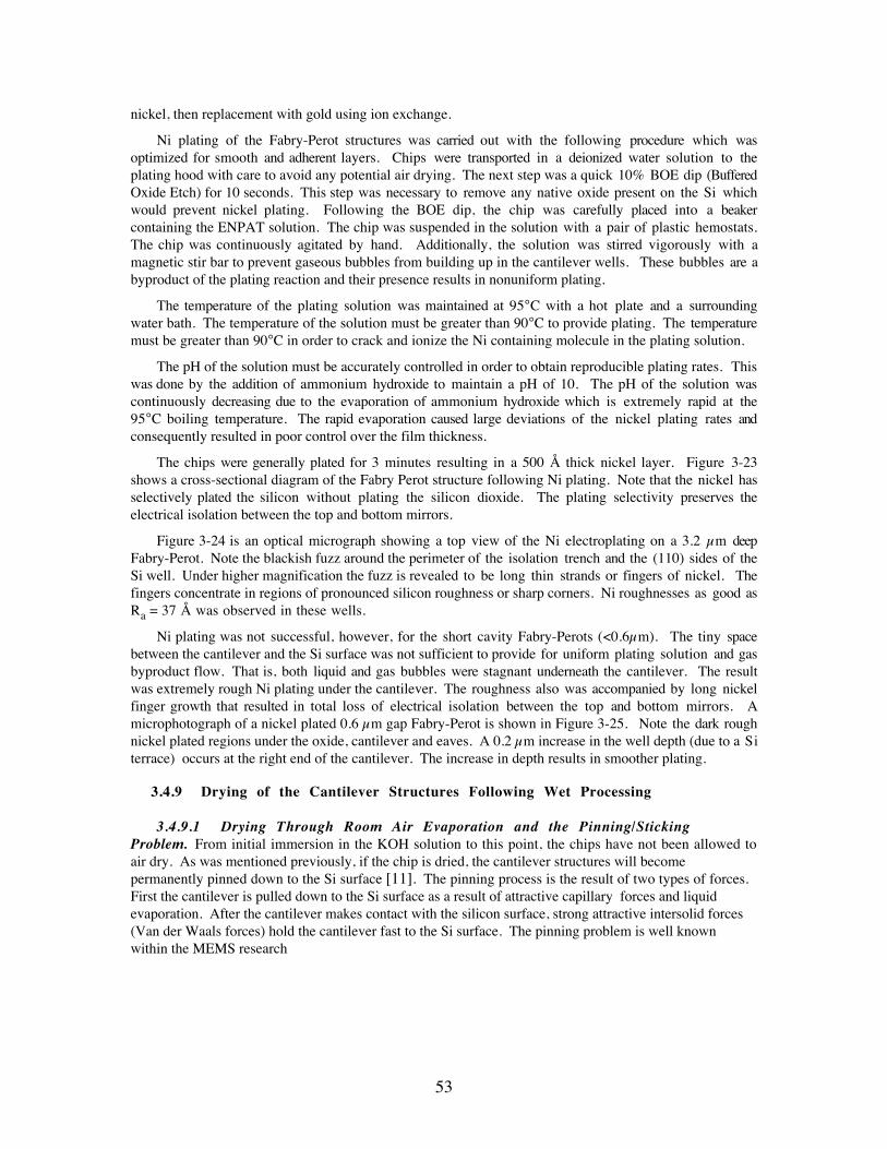
53
nickel, then replacement with gold using ion exchange.
Ni plating of the Fabry-Perot structures was carried out with the following procedure which wasoptimized for smooth and adherent layers. Chips were transported in a deionized water solution to theplating hood with care to avoid any potential air drying. The next step was a quick 10% BOE dip (BufferedOxide Etch) for 10 seconds. This step was necessary to remove any native oxide present on the Si whichwould prevent nickel plating. Following the BOE dip, the chip was carefully placed into a beakercontaining the ENPAT solution. The chip was suspended in the solution with a pair of plastic hemostats.The chip was continuously agitated by hand. Additionally, the solution was stirred vigorously with amagnetic stir bar to prevent gaseous bubbles from building up in the cantilever wells. These bubbles are abyproduct of the plating reaction and their presence results in nonuniform plating.
The temperature of the plating solution was maintained at 95°C with a hot plate and a surroundingwater bath. The temperature of the solution must be greater than 90°C to provide plating. The temperaturemust be greater than 90°C in order to crack and ionize the Ni containing molecule in the plating solution.
The pH of the solution must be accurately controlled in order to obtain reproducible plating rates. Thiswas done by the addition of ammonium hydroxide to maintain a pH of 10. The pH of the solution wascontinuously decreasing due to the evaporation of ammonium hydroxide which is extremely rapid at the95°C boiling temperature. The rapid evaporation caused large deviations of the nickel plating rates andconsequently resulted in poor control over the film thickness.
The chips were generally plated for 3 minutes resulting in a 500 � thick nickel layer. Figure 3-23shows a cross-sectional diagram of the Fabry Perot structure following Ni plating. Note that the nickel hasselectively plated the silicon without plating the silicon dioxide. The plating selectivity preserves theelectrical isolation between the top and bottom mirrors.
Figure 3-24 is an optical micrograph showing a top view of the Ni electroplating on a 3.2 µm deepFabry-Perot. Note the blackish fuzz around the perimeter of the isolation trench and the (110) sides of theSi well. Under higher magnification the fuzz is revealed to be long thin strands or fingers of nickel. Thefingers concentrate in regions of pronounced silicon roughness or sharp corners. Ni roughnesses as good asRaÊ=Ê37 � was observed in these wells.
Ni plating was not successful, however, for the short cavity Fabry-Perots (<0.6µm). The tiny spacebetween the cantilever and the Si surface was not sufficient to provide for uniform plating solution and gasbyproduct flow. That is, both liquid and gas bubbles were stagnant underneath the cantilever. The resultwas extremely rough Ni plating under the cantilever. The roughness also was accompanied by long nickelfinger growth that resulted in total loss of electrical isolation between the top and bottom mirrors. Amicrophotograph of a nickel plated 0.6 µm gap Fabry-Perot is shown in Figure 3-25. Note the dark roughnickel plated regions under the oxide, cantilever and eaves. A 0.2 µm increase in the well depth (due to a Siterrace) occurs at the right end of the cantilever. The increase in depth results in smoother plating.
3.4.9 Drying of the Cantilever Structures Following Wet Processing
3.4.9.1 Drying Through Room Air Evaporation and the Pinning/StickingProblem. From initial immersion in the KOH solution to this point, the chips have not been allowed toair dry. As was mentioned previously, if the chip is dried, the cantilever structures will becomepermanently pinned down to the Si surface [11]. The pinning process is the result of two types of forces.First the cantilever is pulled down to the Si surface as a result of attractive capillary forces and liquidevaporation. After the cantilever makes contact with the silicon surface, strong attractive intersolid forces(Van der Waals forces) hold the cantilever fast to the Si surface. The pinning problem is well knownwithin the MEMS research

54
Si SubstrateSi (111)
Ni Plates Si Not SiO2
SiO2
Ni
Figure 3-23. A cross-sectional diagram of the Fabry-Perot structure following Ni plating. The Ni hasplated only the Si and not the SiO2 preserving the electrical isolation between the top and bottom mirrors.
Figure 3-24. An optical micrograph of a Ni plated 3.2 µm cavity Fabry-Perot.
Figure 3-25. An optical micrograph of a Ni plated 0.6 µm air gap Fabry-Perot. Note the rough Ni platingunder the cantilever and oxide eaves. The roughness is a consequence of poor plating solution and gastransport in the narrow gap.
community. Most researchers fabricating air gap micro-mechanical Fabry-Perots avoid the pinning problemby using dry etching methods to remove the sacrificial layer [15]. However, dry etching methods aregenerally isotropic, and consequently are not compatible with our crystal orientation dependent technique.
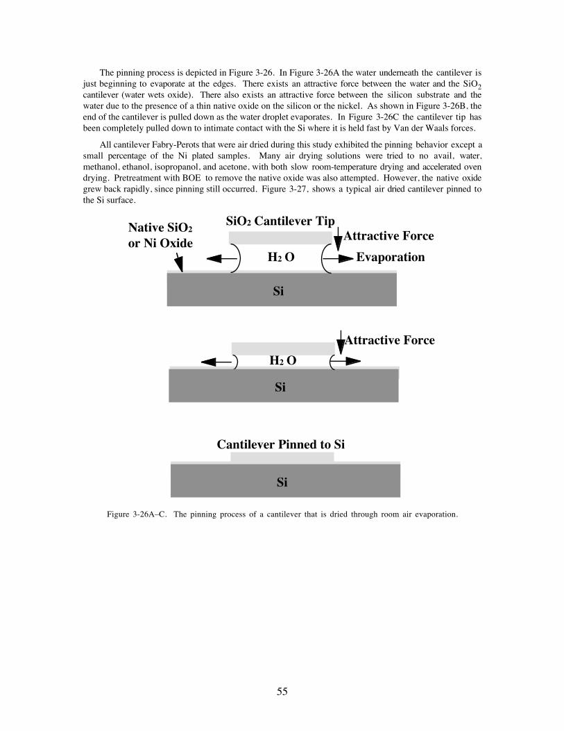
55
The pinning process is depicted in Figure 3-26. In Figure 3-26A the water underneath the cantilever isjust beginning to evaporate at the edges. There exists an attractive force between the water and the SiO2cantilever (water wets oxide). There also exists an attractive force between the silicon substrate and thewater due to the presence of a thin native oxide on the silicon or the nickel. As shown in Figure 3-26B, theend of the cantilever is pulled down as the water droplet evaporates. In Figure 3-26C the cantilever tip hasbeen completely pulled down to intimate contact with the Si where it is held fast by Van der Waals forces.
All cantilever Fabry-Perots that were air dried during this study exhibited the pinning behavior except asmall percentage of the Ni plated samples. Many air drying solutions were tried to no avail, water,methanol, ethanol, isopropanol, and acetone, with both slow room-temperature drying and accelerated ovendrying. Pretreatment with BOE to remove the native oxide was also attempted. However, the native oxidegrew back rapidly, since pinning still occurred. Figure 3-27, shows a typical air dried cantilever pinned tothe Si surface.
Si
H2 O
Attractive Force
Si
Cantilever Pinned to Si
SiO2 Cantilever Tip
Si
H2 O Evaporation
Attractive ForceNative SiO2
or Ni Oxide
Figure 3-26AÐC. The pinning process of a cantilever that is dried through room air evaporation.
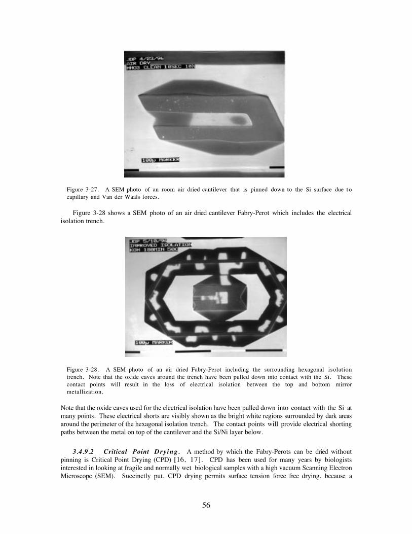
56
Figure 3-27. A SEM photo of an room air dried cantilever that is pinned down to the Si surface due tocapillary and Van der Waals forces.
Figure 3-28 shows a SEM photo of an air dried cantilever Fabry-Perot which includes the electricalisolation trench.
Figure 3-28. A SEM photo of an air dried Fabry-Perot including the surrounding hexagonal isolationtrench. Note that the oxide eaves around the trench have been pulled down into contact with the Si. Thesecontact points will result in the loss of electrical isolation between the top and bottom mirrormetallization.
Note that the oxide eaves used for the electrical isolation have been pulled down into contact with the Si atmany points. These electrical shorts are visibly shown as the bright white regions surrounded by dark areasaround the perimeter of the hexagonal isolation trench. The contact points will provide electrical shortingpaths between the metal on top of the cantilever and the Si/Ni layer below.
3.4.9.2 Critical Point Drying. A method by which the Fabry-Perots can be dried withoutpinning is Critical Point Drying (CPD) [16, 17]. CPD has been used for many years by biologistsinterested in looking at fragile and normally wet biological samples with a high vacuum Scanning ElectronMicroscope (SEM). Succinctly put, CPD drying permits surface tension force free drying, because a
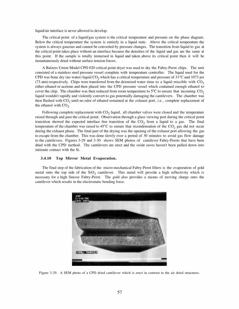
57
liquid/air interface is never allowed to develop.
The critical point of a liquid/gas system is the critical temperature and pressure on the phase diagram.Below the critical temperature the system is entirely in a liquid state. Above the critical temperature thesystem is always gaseous and cannot be converted by pressure changes. The transition from liquid to gas atthe critical point takes place without an interface because the densities of the liquid and gas are the same atthis point. If the sample is totally immersed in liquid and taken above its critical point then it will beinstantaneously dried without surface tension forces.
A Balzers Union Model CPD 020 critical point dryer was used to dry the Fabry-Perot chips. The unitconsisted of a stainless steel pressure vessel complete with temperature controller. The liquid used for theCPD was bone dry (no water) liquid CO2 which has a critical temperature and pressure of 31°C and 1073 psi(73 atm) respectively. Chips were transferred from the deionized water rinse to a liquid miscible with CO2either ethanol or acetone and then placed into the CPD pressure vessel which contained enough ethanol tocover the chip. The chamber was then reduced from room temperature to 5°C to ensure that incoming CO2liquid wouldn't rapidly and violently convert to gas potentially damaging the cantilevers. The chamber wasthen flushed with CO2 until no odor of ethanol remained at the exhaust port, i.e., complete replacement ofthe ethanol with CO2.
Following complete replacement with CO2 liquid, all chamber valves were closed and the temperatureraised through and past the critical point. Observation through a glass viewing port during the critical pointtransition showed the expected interface free transition of the CO2 from a liquid to a gas. The finaltemperature of the chamber was raised to 45°C to ensure that recondensation of the CO2 gas did not occurduring the exhaust phase. The final part of the drying was the opening of the exhaust port allowing the gasto escape from the chamber. This was done slowly over a period of 30 minutes to avoid gas flow damageto the cantilevers. Figures 3-29 and 3-30 shows SEM photos of cantilever Fabry-Perots that have beendried with the CPD method. The cantilevers are erect and the oxide eaves haven't been pulled down intointimate contact with the Si.
3.4.10 Top Mirror Metal Evaporation.
The final step of the fabrication of the micro-mechanical Fabry-Perot filters is the evaporation of goldmetal onto the top side of the SiO2 cantilever. This metal will provide a high reflectivity which isnecessary for a high finesse Fabry-Perot. The gold also provides a means of moving charge onto thecantilever which results in the electrostatic bending force.
Figure 3-29. A SEM photo of a CPD dried cantilever which is erect in contrast to the air dried structures.
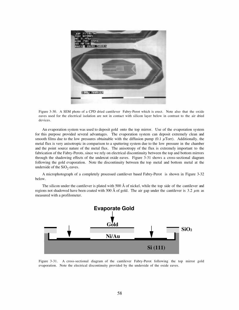
58
Figure 3-30. A SEM photo of a CPD dried cantilever Fabry-Perot which is erect. Note also that the oxideeaves used for the electrical isolation are not in contact with silicon layer below in contrast to the air drieddevices.
An evaporation system was used to deposit gold onto the top mirror. Use of the evaporation systemfor this purpose provided several advantages. The evaporation system can deposit extremely clean andsmooth films due to the low pressures obtainable with the diffusion pump (0.1 µTorr). Additionally, themetal flux is very anisotropic in comparison to a sputtering system due to the low pressure in the chamberand the point source nature of the metal flux. The anisotropy of the flux is extremely important to thefabrication of the Fabry-Perots, since we rely on electrical discontinuity between the top and bottom mirrorsthrough the shadowing effects of the undercut oxide eaves. Figure 3-31 shows a cross-sectional diagramfollowing the gold evaporation. Note the discontinuity between the top metal and bottom metal at theunderside of the SiO2 eaves.
A microphotograph of a completely processed cantilever based Fabry-Perot is shown in Figure 3-32below.
The silicon under the cantilever is plated with 500 � of nickel, while the top side of the cantilever andregions not shadowed have been coated with 300 � of gold. The air gap under the cantilever is 3.2 µm asmeasured with a profilometer.
Evaporate Gold
Si Substrate
GoldSiO2
Si (111)
Ni/Au
Figure 3-31. A cross-sectional diagram of the cantilever Fabry-Perot following the top mirror goldevaporation. Note the electrical discontinuity provided by the underside of the oxide eaves.
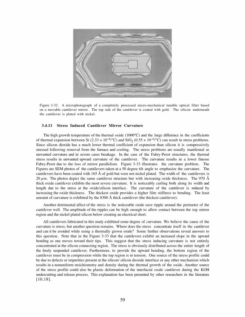
59
Figure 3-32. A microphotograph of a completely processed micro-mechanical tunable optical filter basedon a movable cantilever mirror. The top side of the cantilever is coated with gold. The silicon underneaththe cantilever is plated with nickel.
3.4.11 Stress Induced Cantilever Mirror Curvature
The high growth temperature of the thermal oxide (1000¡C) and the large difference in the coefficientsof thermal expansion between Si (2.33 ´ 10-6/°C) and SiO2 (0.55 ´ 10-6/°C) can result in stress problems.Since silicon dioxide has a much lower thermal coefficient of expansion than silicon it is compressivelystressed following removal from the furnace and cooling. The stress problems are usually manifested asunwanted curvature and in severe cases breakage. In the case of the Fabry-Perot structures, the thermalstress results in unwanted upward curvature of the cantilever. The curvature results in a lower finesseFabry-Perot due to the loss of mirror parallelism. Figure 3-33 illustrates the curvature problem. TheFigures are SEM photos of the cantilevers taken at a 50 degree tilt angle to emphasize the curvature. Thecantilevers have been coated with 165 � of gold but were not nickel plated. The width of the cantilevers is20 µm. The photos depict the same cantilever structure but with increasing oxide thickness. The 970 �thick oxide cantilever exhibits the most severe curvature. It is noticeably curling both along its width andlength due to the stress at the oxide/silicon interface. The curvature of the cantilever is reduced byincreasing the oxide thickness. The thickest oxide provides a higher film stiffness to bending. The leastamount of curvature is exhibited by the 8300 � thick cantilever (the thickest cantilever).
Another detrimental affect of the stress is the noticeable oxide eave ripple around the perimeter of thecantilever well. The amplitude of the ripples can be high enough to allow contact between the top mirrorregion and the nickel plated silicon below creating an electrical short.
All cantilevers fabricated in this study exhibited some degree of curvature. We believe the cause of thecurvature is stress, but another question remains. Where does the stress concentrate itself in the cantileverand can it be avoided while using a thermally grown oxide? Some further observations reveal answers tothis question. Note that in the Figure 3-33 that the cantilevers exhibit an increased slope in the upwardbending as one moves toward their tips. This suggest that the stress inducing curvature is not entirelyconcentrated at the silicon connecting region. The stress is obviously distributed across the entire length ofthe freely suspended cantilever. Furthermore, to provide the upward bending, the bottom region of thecantilever must be in compression while the top region is in tension. One source of the stress profile couldbe due to defects or impurities present at the silicon/ silicon dioxide interface or any other mechanism whichresults in a nonuniform stoichiometry and density during the thermal growth of the oxide. Another sourceof the stress profile could also be plastic deformation of the interfacial oxide cantilever during the KOHundercutting and release process. This explanation has been presented by other researchers in the literature[10,18].
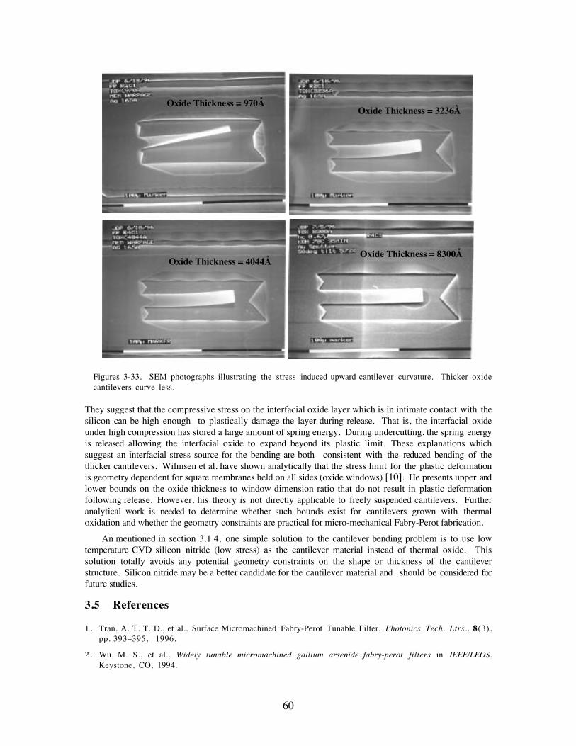
60
Oxide Thickness = 970�Oxide Thickness = 3236�
Oxide Thickness = 4044�Oxide Thickness = 8300�
Figures 3-33. SEM photographs illustrating the stress induced upward cantilever curvature. Thicker oxidecantilevers curve less.
They suggest that the compressive stress on the interfacial oxide layer which is in intimate contact with thesilicon can be high enough to plastically damage the layer during release. That is, the interfacial oxideunder high compression has stored a large amount of spring energy. During undercutting, the spring energyis released allowing the interfacial oxide to expand beyond its plastic limit. These explanations whichsuggest an interfacial stress source for the bending are both consistent with the reduced bending of thethicker cantilevers. Wilmsen et al. have shown analytically that the stress limit for the plastic deformationis geometry dependent for square membranes held on all sides (oxide windows) [10]. He presents upper andlower bounds on the oxide thickness to window dimension ratio that do not result in plastic deformationfollowing release. However, his theory is not directly applicable to freely suspended cantilevers. Furtheranalytical work is needed to determine whether such bounds exist for cantilevers grown with thermaloxidation and whether the geometry constraints are practical for micro-mechanical Fabry-Perot fabrication.
An mentioned in section 3.1.4, one simple solution to the cantilever bending problem is to use lowtemperature CVD silicon nitride (low stress) as the cantilever material instead of thermal oxide. Thissolution totally avoids any potential geometry constraints on the shape or thickness of the cantileverstructure. Silicon nitride may be a better candidate for the cantilever material and should be considered forfuture studies.
3.5 References
1 . Tran, A. T. T. D., et al., Surface Micromachined Fabry-Perot Tunable Filter, Photonics Tech. Ltrs., 8(3),pp.Ê393Ð395, 1996.
2 . Wu, M. S., et al., Widely tunable micromachined gallium arsenide fabry-perot filters in IEEE/LEOS,Keystone, CO, 1994.
61
3 . Petersen, K. E., Silicon as a mechanical material, Proceedings of the IEEE, 70(5), pp. 420Ð457, 1982.
4 . Schwartz, B., Chemical Etching of Silicon, J. of the Electrochem. Soc., 1976. (12): pp. 1903Ð1909.
5 . Seidal, H., et al., Anisotropic Etching of Crystalline Silicon in Alkaline Solutions, J. of the Electrochem.Soc .,. 137(11), pp. 3626Ð3632, 1990.
6 . Seidal, H., Crystalline Semiconductor Micromachining in Transducers '87 Rec. of the 4th Int. Conf. onSolid-State Sensors and Actuators, pp. 120Ð125, 1987.
7 . Waggener, H. A., R. C. Kragness, and A. L. Taylor, KOH Etching of Si, Elect.,.40, p. 274, 1967.
8 . Choi, W. S. and J. G. Smits, A method to etch undoped silicon cantilever beams, J. of Microelectro.Sys .,. 2(2), pp.Ê82Ð86, 1993.
9.Sze, S. M., Oxidation and Film Deposition, in Semiconductor Devices: Physics and Technology, MurrayHill, NJ, pp.Ê360Ð362, 1985.
10. Wilmsen, C. W., E. G. Thompson, and G. H. Meissner, Buckling of Thermally-Grown SiO2 Films, IEEETrans. Elect. Dev., (1), p. 122.,1972.
11. Mastrangelo, C. H. and C. H. Hsu, Mechanical Stability and Adhesion of Microstructures: Part I: BasicTheory, J.Êof Micro-mech. Sys., 2(1), pp. 33Ð43, 1993.
12. Queau, E., et al., Electroless Metal Deposition as a Useful Tool For Microelectronics and Microstructures,J. of Electrochem. Soc., (1), pp. 65Ð69, 1994.
13. Transene Inc. Literature, Advanced Materials For Electronics, Transene Inc., Rowley, Mass., pp. 126Ð127,1981.
14. Transene Inc. Literature, Advanced Materials For Electronics, Transene Inc., Rowley, Mass., p. 138Ð139,1981.
15. Harris Jr., J. S., M. C. Larson, and A. R. Massengale, Coupled -cavity laser diode with micromachinedexternal mirrors in IEEE/LEOS 1996 Summer Topical Meetings: Optical MEMS and Their Applications.Keystone, CO, pp. 31Ð32, 1996.
16. Burstyn, H. P., Critical point drying: Application of the physics of the PVT surface to electronmicroscopy, Am. J. of Phys., 43(5), pp. 414-419, 1975.
17. Ho, S. T., et al., High index contrast mirrors for optical microcavities, App. Phys. Ltrs., 57(14),ppÊ1387Ð1389, 1990.
18. Jolly, R. D. and R. S. Muller, Miniature Cantilever Beams Fabricated by Anisotropic Etching of Silicon,J. of Electrochem. Soc., Solid State Science and Technology, 127(12), pp. 2750Ð2754, 1980.

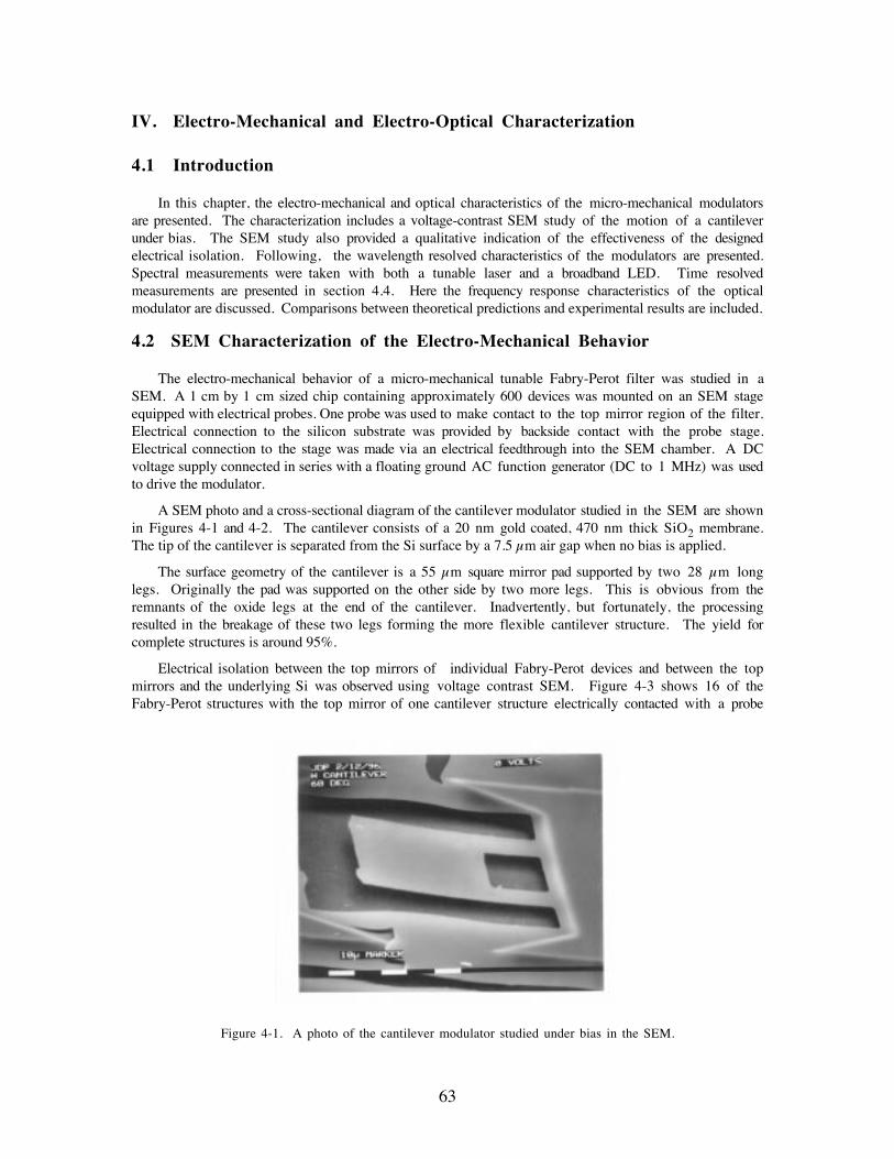
63
IV. Electro-Mechanical and Electro-Optical Characterization
4.1 Introduction
In this chapter, the electro-mechanical and optical characteristics of the micro-mechanical modulatorsare presented. The characterization includes a voltage-contrast SEM study of the motion of a cantileverunder bias. The SEM study also provided a qualitative indication of the effectiveness of the designedelectrical isolation. Following, the wavelength resolved characteristics of the modulators are presented.Spectral measurements were taken with both a tunable laser and a broadband LED. Time resolvedmeasurements are presented in section 4.4. Here the frequency response characteristics of the opticalmodulator are discussed. Comparisons between theoretical predictions and experimental results are included.
4.2 SEM Characterization of the Electro-Mechanical Behavior
The electro-mechanical behavior of a micro-mechanical tunable Fabry-Perot filter was studied in aSEM. A 1 cm by 1 cm sized chip containing approximately 600 devices was mounted on an SEM stageequipped with electrical probes. One probe was used to make contact to the top mirror region of the filter.Electrical connection to the silicon substrate was provided by backside contact with the probe stage.Electrical connection to the stage was made via an electrical feedthrough into the SEM chamber. A DCvoltage supply connected in series with a floating ground AC function generator (DC to 1 MHz) was usedto drive the modulator.
A SEM photo and a cross-sectional diagram of the cantilever modulator studied in the SEM are shownin Figures 4-1 and 4-2. The cantilever consists of a 20 nm gold coated, 470 nm thick SiO2 membrane.The tip of the cantilever is separated from the Si surface by a 7.5 µm air gap when no bias is applied.
The surface geometry of the cantilever is a 55 µm square mirror pad supported by two 28 µm longlegs. Originally the pad was supported on the other side by two more legs. This is obvious from theremnants of the oxide legs at the end of the cantilever. Inadvertently, but fortunately, the processingresulted in the breakage of these two legs forming the more flexible cantilever structure. The yield forcomplete structures is around 95%.
Electrical isolation between the top mirrors of individual Fabry-Perot devices and between the topmirrors and the underlying Si was observed using voltage contrast SEM. Figure 4-3 shows 16 of theFabry-Perot structures with the top mirror of one cantilever structure electrically contacted with a probe
Figure 4-1. A photo of the cantilever modulator studied under bias in the SEM.

64
SiO2470nm
7.5µm Air Gap
Si (111)
14µm28µm55µm
55µm Gold200�
Figure 4-2. A cross-sectional schematic of the cantilever modulator studied in the SEM.
marker=1mm
Figure 4-3. A SEM photo of the cantilever modulator without an applied bias.
without applied bias. Note the hexagonal electrical isolation trench delineating the structure. The extent ofthe probed cantilever including the isolation trench is 250 µm by 400 µm. Figure 4-4 shows the samecantilever but with 45 V of DC bias. The white or brighter regions indicate the area with a higherpotential. Note that the hexagonal trench clearly electrically isolates the top mirror of the device from thetop mirrors of adjacent Fabry-Perots. Also the bright top mirror or cantilever is shown to be electricallyisolated from the darker Si well below. This indicates the required electrical isolation between the top andbottom mirrors.
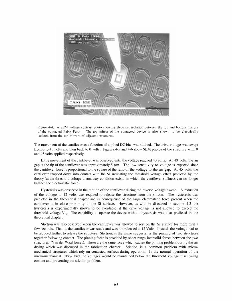
65
marker=1mm
Figure 4-4. A SEM voltage contrast photo showing electrical isolation between the top and bottom mirrorsof the contacted Fabry-Perot. The top mirror of the contacted device is also shown to be electricallyisolated from the top mirrors of adjacent structures.
The movement of the cantilever as a function of applied DC bias was studied. The drive voltage was sweptfrom 0 to 45 volts and then back to 0 volts. Figures 4-5 and 4-6 show SEM photos of the structure with 0and 45 volts applied respectively.
Little movement of the cantilever was observed until the voltage reached 40 volts. At 40 volts the airgap at the tip of the cantilever was approximately 5 µm. The low sensitivity to voltage is expected sincethe cantilever force is proportional to the square of the ratio of the voltage to the air gap. At 45 volts thecantilever snapped down into contact with the Si indicating the threshold voltage effect predicted by thetheory (at the threshold voltage a runaway condition exists in which the cantilever stiffness can no longerbalance the electrostatic force).
Hysteresis was observed in the motion of the cantilever during the reverse voltage sweep. A reductionof the voltage to 12 volts was required to release the structure from the silicon. The hysteresis waspredicted in the theoretical chapter and is consequence of the large electrostatic force present when thecantilever is in close proximity to the Si surface. However, as will be discussed in section 4.3 thehysteresis is experimentally shown to be avoidable, if the drive voltage is not allowed to exceed thethreshold voltage Vth. The capability to operate the device without hysteresis was also predicted in thetheoretical chapter.
Stiction was also observed when the cantilever was allowed to rest on the Si surface for more than afew seconds. That is, the cantilever was stuck and was not released at 12 Volts. Instead, the voltage had tobe reduced further to release the structure. Stiction, as the name suggests, is the pinning of two structurestogether following contact. The pinning force is provided by short range intersolid forces between the twostructures (Van der Waal forces). These are the same force which causes the pinning problem during the airdrying which was discussed in the fabrication chapter. Stiction is a common problem with micro-mechanical structures which rely on contacted surfaces during operation. In the normal operation of themicro-mechanical Fabry-Perot the voltages would be maintained below the threshold voltage disallowingcontact and preventing the stiction problem.
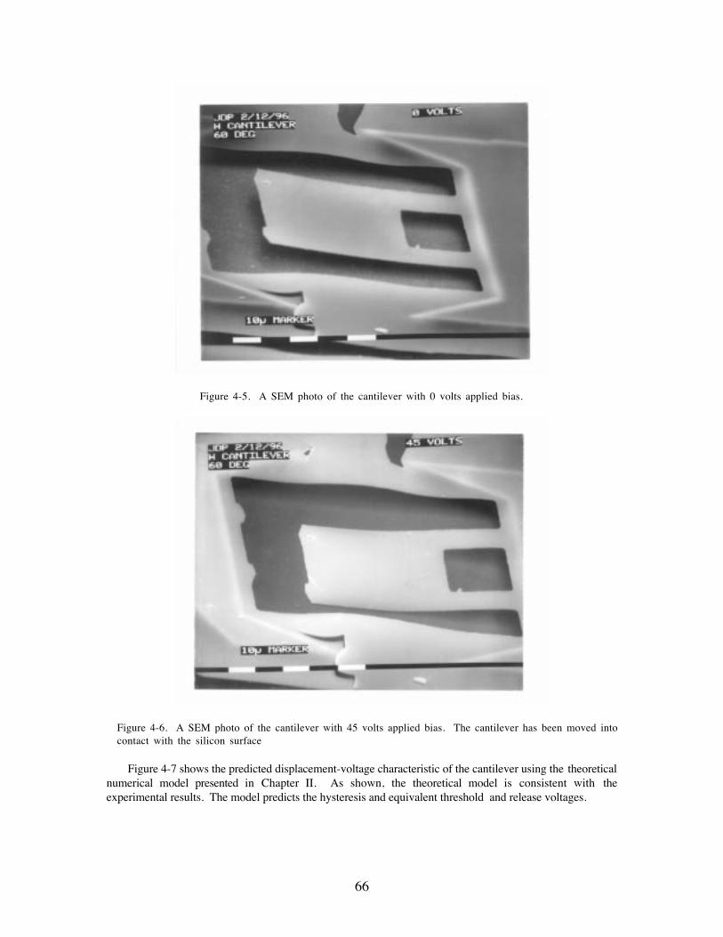
66
Figure 4-5. A SEM photo of the cantilever with 0 volts applied bias.
Figure 4-6. A SEM photo of the cantilever with 45 volts applied bias. The cantilever has been moved intocontact with the silicon surface
Figure 4-7 shows the predicted displacement-voltage characteristic of the cantilever using the theoreticalnumerical model presented in Chapter II. As shown, the theoretical model is consistent with theexperimental results. The model predicts the hysteresis and equivalent threshold and release voltages.
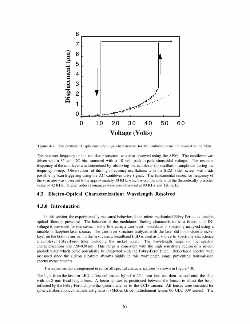
67
0
1
2
3
4
5
6
7
8
0 1 0 2 0 3 0 4 0 5 0 6 0
Voltage (Volts)
Dis
plac
emen
t (µ
m)
Figure 4-7. The predicted Displacement-Voltage characteristic for the cantilever structure studied in the SEM.
The resonant frequency of the cantilever structure was also observed using the SEM. The cantilever wasdriven with a 35 volt DC bias summed with a 10 volt peak-to-peak sinusoidal voltage. The resonantfrequency of the cantilever was determined by observing the cantilever tip oscillation amplitude during thefrequency sweep. Observation of the high frequency oscillations with the SEM video screen was madepossible by scan triggering using the AC cantilever drive signal. The fundamental resonance frequency ofthe structure was observed to be approximately 40 KHz which is comparable with the theoretically predictedvalue of 42 KHz. Higher order resonances were also observed at 80 KHz and 120 KHz.
4.3 Electro-Optical Characterization: Wavelength Resolved
4.3.0 Introduction
In this section, the experimentally measured behavior of the micro-mechanical Fabry-Perots as tunableoptical filters is presented. The behavior of the modulator filtering characteristics as a function of DCvoltage is presented for two cases. In the first case, a cantilever modulator is spectrally analyzed using atunable Ti-Sapphire laser source. The cantilever structure analyzed with the laser did not include a nickellayer on the bottom mirror. In the next case, a broadband LED is used as a source to spectrally characterizea cantilever Fabry-Perot filter including the nickel layer. The wavelength range for the spectralcharacterizations was 720Ð920 nm. This range is consistent with the high sensitivity region of a siliconphotodetector which could potentially be integrated with the Fabry-Perot filter. Reflectance spectra weremeasured since the silicon substrate absorbs highly in this wavelength range preventing transmissionspectra measurements.
The experimental arrangement used for all spectral characterizations is shown in Figure 4-8.
The light from the laser or LED is first collimated by a f = 25.4 mm lens and then focused onto the chipwith an 8 mm focal length lens. A beam splitter is positioned between the lenses to direct the beamreflected by the Fabry-Perot chip to the spectrometer or to the CCD camera. All lenses were corrected forspherical aberration, coma, and astigmatism (Melles Griot multielement lenses 06 GLC 00# series). The
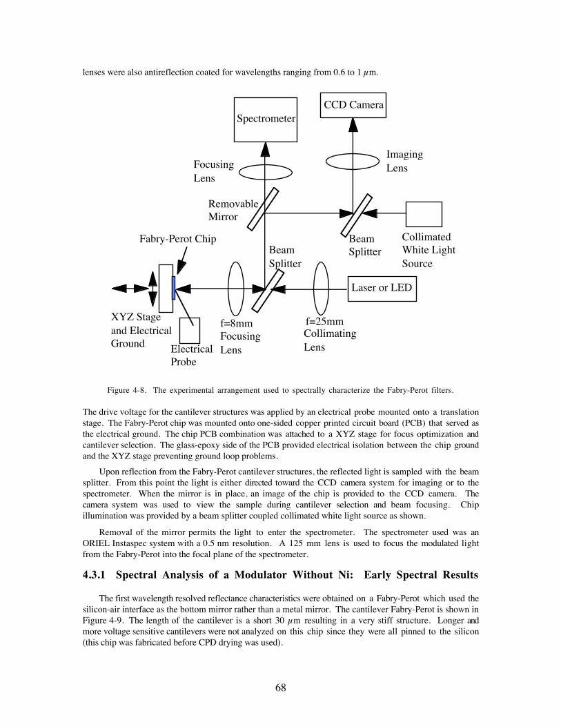
68
lenses were also antireflection coated for wavelengths ranging from 0.6 to 1 µm.
f=25mmf=8mmFocusingLens
BeamSplitter
CollimatingLens
Fabry-Perot Chip
ElectricalProbe
XYZ Stageand ElectricalGround
CCD Camera
Laser or LED
Spectrometer
CollimatedWhite LightSource
ImagingLensFocusing
Lens
BeamSplitter
RemovableMirror
Figure 4-8. The experimental arrangement used to spectrally characterize the Fabry-Perot filters.
The drive voltage for the cantilever structures was applied by an electrical probe mounted onto a translationstage. The Fabry-Perot chip was mounted onto one-sided copper printed circuit board (PCB) that served asthe electrical ground. The chip PCB combination was attached to a XYZ stage for focus optimization andcantilever selection. The glass-epoxy side of the PCB provided electrical isolation between the chip groundand the XYZ stage preventing ground loop problems.
Upon reflection from the Fabry-Perot cantilever structures, the reflected light is sampled with the beamsplitter. From this point the light is either directed toward the CCD camera system for imaging or to thespectrometer. When the mirror is in place, an image of the chip is provided to the CCD camera. Thecamera system was used to view the sample during cantilever selection and beam focusing. Chipillumination was provided by a beam splitter coupled collimated white light source as shown.
Removal of the mirror permits the light to enter the spectrometer. The spectrometer used was anORIEL Instaspec system with a 0.5 nm resolution. A 125 mm lens is used to focus the modulated lightfrom the Fabry-Perot into the focal plane of the spectrometer.
4.3.1 Spectral Analysis of a Modulator Without Ni: Early Spectral Results
The first wavelength resolved reflectance characteristics were obtained on a Fabry-Perot which used thesilicon-air interface as the bottom mirror rather than a metal mirror. The cantilever Fabry-Perot is shown inFigure 4-9. The length of the cantilever is a short 30 µm resulting in a very stiff structure. Longer andmore voltage sensitive cantilevers were not analyzed on this chip since they were all pinned to the silicon(this chip was fabricated before CPD drying was used).
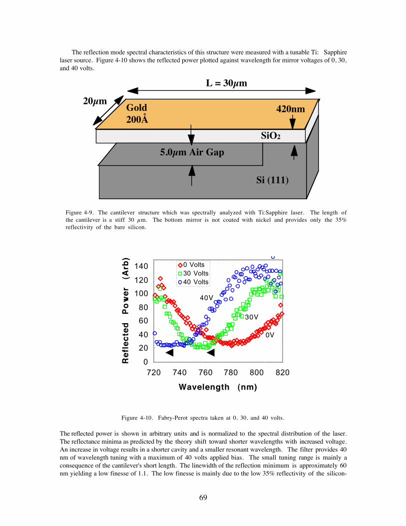
69
The reflection mode spectral characteristics of this structure were measured with a tunable Ti: Sapphirelaser source. Figure 4-10 shows the reflected power plotted against wavelength for mirror voltages of 0, 30,and 40 volts.
SiO2
420nm
5.0µm Air Gap
Si (111)
L = 30µm
Gold200�
20µm
Figure 4-9. The cantilever structure which was spectrally analyzed with Ti:Sapphire laser. The length ofthe cantilever is a stiff 30 µm. The bottom mirror is not coated with nickel and provides only the 35%reflectivity of the bare silicon.
0
20
40
60
80
100
120
140
720 740 760 780 800 820
Wavelength (nm)
Re
fle
cte
d
Po
we
r (A
rb)
0 Volts30 Volts40 Volts
0V
30V
40V
Figure 4-10. Fabry-Perot spectra taken at 0, 30, and 40 volts.
The reflected power is shown in arbitrary units and is normalized to the spectral distribution of the laser.The reflectance minima as predicted by the theory shift toward shorter wavelengths with increased voltage.An increase in voltage results in a shorter cavity and a smaller resonant wavelength. The filter provides 40nm of wavelength tuning with a maximum of 40 volts applied bias. The small tuning range is mainly aconsequence of the cantilever's short length. The linewidth of the reflection minimum is approximately 60nm yielding a low finesse of 1.1. The low finesse is mainly due to the low 35% reflectivity of the silicon-
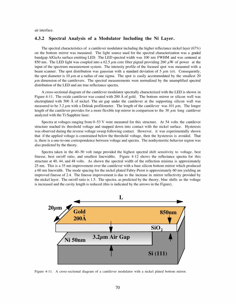
70
air interface.
4.3.2 Spectral Analysis of a Modulator Including the Ni Layer.
The spectral characteristics of a cantilever modulator including the higher reflectance nickel layer (67%)on the bottom mirror was measured. The light source used for the spectral characterization was a gradedbandgap AlGaAs surface emitting LED. The LED spectral width was 100 nm FWHM and was centered at850 nm. The LED light was coupled into a 62.5 µm core fiber pigtail providing 260 µW of power at theinput of the spectrum measurement system. The intensity profile of the focused spot was measured with abeam scanner. The spot distribution was gaussian with a standard deviation of 5 µm (s). Consequently,the spot diameter is 10 µm at a radius of one sigma. The spot is easily accommodated by the smallest 20µm dimension of the cantilevers. The spectral measurements were normalized by the unamplified spectraldistribution of the LED and are true reflectance spectra.
A cross-sectional diagram of the cantilever modulator spectrally characterized with the LED is shown inFigure 4-11. The oxide cantilever was coated with 200 � of gold. The bottom mirror or silicon well waselectroplated with 500 � of nickel. The air gap under the cantilever at the supporting silicon wall wasmeasured to be 3.2 µm with a Dektak profilometer. The length of the cantilever was 101 µm. The longerlength of the cantilever provides for a more flexible top mirror in comparison to the 30 µm long cantileveranalyzed with the Ti:Sapphire laser.
Spectra at voltages ranging from 0Ð53 V were measured for this structure. At 54 volts the cantileverstructure reached its threshold voltage and snapped down into contact with the nickel surface. Hysteresiswas observed during the reverse voltage sweep following contact. However, it was experimentally shownthat if the applied voltage is constrained below the threshold voltage, then the hysteresis is avoided. Thatis, there is a one-to-one correspondence between voltage and spectra. The nonhysteretic behavior region wasalso predicted by the theory.
Spectra taken in the 40Ð50 volt range provided the highest spectral shift sensitivity to voltage, bestfinesse, best on/off ratio, and smallest linewidths. Figure 4-12 shows the reflectance spectra for thisstructure at 40, 44, and 48 volts. As shown the spectral width of the reflection minima is approximately25 nm. This is a 35 nm improvement over the cantilever with a bare silicon bottom mirror which produceda 60 nm linewidth. The mode spacing for the nickel plated Fabry-Perot is approximately 60 nm yielding animproved finesse of 2.4. The finesse improvement is due to the increase in mirror reflectivity provided bythe nickel layer. The on/off ratio is 1.5. The spectra, as predicted by the theory, blue shifts as the voltageis increased and the cavity length is reduced (this is indicated by the arrows in the Figure).
SiO2
850nm
3.2µm Air Gap
Si (111)
L
Gold200�
Ni 50nm
20µm
Figure 4-11. A cross-sectional diagram of a cantilever modulator with a nickel plated bottom mirror.

71
0
1 0
2 0
3 0
4 0
5 0
6 0
7 0
8 0
9 0
100
780 800 820 840 860 880 900 920
Wavelength (nm)
Re
fle
cta
nc
e
(%)
40V44V48V
Figure 4-12. The Fabry-Perot spectra measured at 40, 44, and 48 volts applied bias.
Comparison between theoretical and experimentally measured spectra and threshold voltage has suggestedthat the air gap at the end of the cantilever is 6.27 µm instead of 3.2 µm. The wavelength position of thereflectance minima and the 53 volt threshold voltage are consistent with an air gap of 6.27 µm. The 3.2µm depth as shown in Figure 4-11 was measured with the Dektak profilometer at the supporting siliconwall and not at the tip of the cantilever where the light beam is focused. Measurement of the cantilever tipheight with the Dektak is impossible since the weight of the stylus would collapse the cantilever. TheDektak measurement is valid at the tip when the cantilever is straight. However, as mentioned in thefabrication chapter, the cantilevers curve upward resulting in an increased air gap at the tip (see Figure 3-33). The curvature was due to the high thermal stress between the silicon substrate and the silicon dioxidecantilever before undercutting.
Figure 4-13 shows a comparison between the measured and theoretical spectrum for the cantilever witha 40 volt applied bias. The calculated spectrum assumes ideal, flat and parallel, top and bottom mirrors andan air gap of 6.27 µm.
The measured reflectance wavelength minima are closely predicted by the theory. The maximumreflectance measured experimentally is 86% which is slightly lower but comparable to the calculated valueof 92%. The lower experimental values are probably due to light scattering losses at the mirrors. On theother hand, the finesse, linewidth, and on/off ratio are much poorer than that predicted by the ideal Fabry-Perot theory. The theory predicts a finesse of 13, a linewidth of 4 nm, and an on/off ratio of 9. Reducedperformance is most probably due to the stress induced curvature of the top mirror and the staircase profileof the bottom mirror. The staircase profile was discussed in the fabrication chapter and is a consequence ofa misalignment of the wafer surface with respect to the (111) plane. The depth of the staircase has beenshown to result in air gap variations ranging from 388Ð1700 � underneath the cantilever as measured usingthe Dektak profilometer.
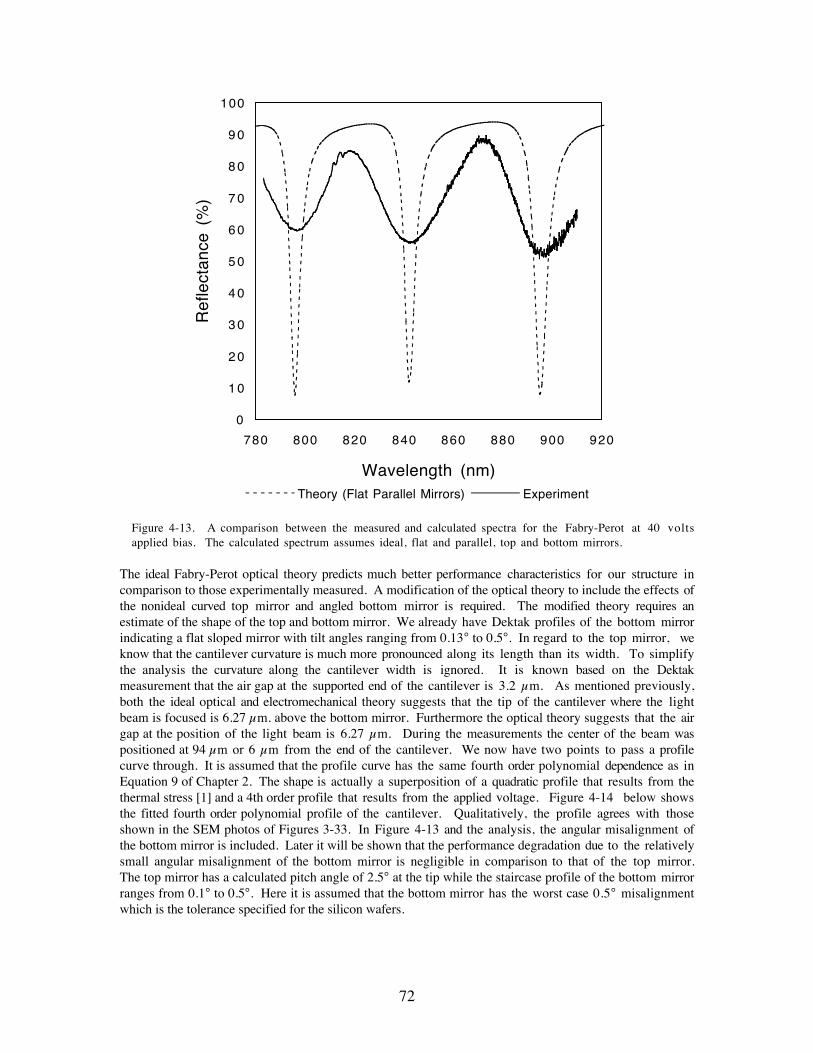
72
0
1 0
2 0
3 0
4 0
5 0
6 0
7 0
8 0
9 0
100
780 800 820 840 860 880 900 920
Wavelength (nm)
Ref
lect
ance
(%
)
Theory (Flat Parallel Mirrors) Experiment
Figure 4-13. A comparison between the measured and calculated spectra for the Fabry-Perot at 40 voltsapplied bias. The calculated spectrum assumes ideal, flat and parallel, top and bottom mirrors.
The ideal Fabry-Perot optical theory predicts much better performance characteristics for our structure incomparison to those experimentally measured. A modification of the optical theory to include the effects ofthe nonideal curved top mirror and angled bottom mirror is required. The modified theory requires anestimate of the shape of the top and bottom mirror. We already have Dektak profiles of the bottom mirrorindicating a flat sloped mirror with tilt angles ranging from 0.13° to 0.5°. In regard to the top mirror, weknow that the cantilever curvature is much more pronounced along its length than its width. To simplifythe analysis the curvature along the cantilever width is ignored. It is known based on the Dektakmeasurement that the air gap at the supported end of the cantilever is 3.2 µm. As mentioned previously,both the ideal optical and electromechanical theory suggests that the tip of the cantilever where the lightbeam is focused is 6.27 µm. above the bottom mirror. Furthermore the optical theory suggests that the airgap at the position of the light beam is 6.27 µm. During the measurements the center of the beam waspositioned at 94 µm or 6 µm from the end of the cantilever. We now have two points to pass a profilecurve through. It is assumed that the profile curve has the same fourth order polynomial dependence as inEquation 9 of Chapter 2. The shape is actually a superposition of a quadratic profile that results from thethermal stress [1] and a 4th order profile that results from the applied voltage. Figure 4-14 below showsthe fitted fourth order polynomial profile of the cantilever. Qualitatively, the profile agrees with thoseshown in the SEM photos of Figures 3-33. In Figure 4-13 and the analysis, the angular misalignment ofthe bottom mirror is included. Later it will be shown that the performance degradation due to the relativelysmall angular misalignment of the bottom mirror is negligible in comparison to that of the top mirror.The top mirror has a calculated pitch angle of 2.5° at the tip while the staircase profile of the bottom mirrorranges from 0.1° to 0.5°. Here it is assumed that the bottom mirror has the worst case 0.5° misalignmentwhich is the tolerance specified for the silicon wafers.
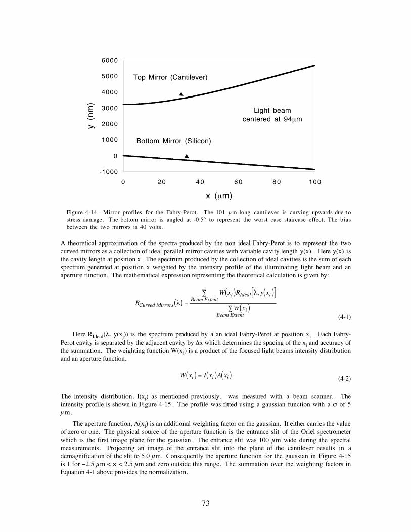
73
-1000
0
1000
2000
3000
4000
5000
6000
0 2 0 4 0 6 0 8 0 100
x (mm)
y (n
m)
Light beamcentered at 94mm
Top Mirror (Cantilever)
Bottom Mirror (Silicon)
Figure 4-14. Mirror profiles for the Fabry-Perot. The 101 µm long cantilever is curving upwards due tostress damage. The bottom mirror is angled at -0.5¡ to represent the worst case staircase effect. The biasbetween the two mirrors is 40 volts.
A theoretical approximation of the spectra produced by the non ideal Fabry-Perot is to represent the twocurved mirrors as a collection of ideal parallel mirror cavities with variable cavity length y(x). Here y(x) isthe cavity length at position x. The spectrum produced by the collection of ideal cavities is the sum of eachspectrum generated at position x weighted by the intensity profile of the illuminating light beam and anaperture function. The mathematical expression representing the theoretical calculation is given by:
R
W x R y x
W xCurved Mirrors
i Ideal iBeam Extent
iBeam Extent
l
l
( ) =
( ) ( )[ ]å
( )å
,
(4-1)
Here RIdeal(l, y(xj)) is the spectrum produced by a an ideal Fabry-Perot at position xi. Each Fabry-Perot cavity is separated by the adjacent cavity by Dx which determines the spacing of the xi and accuracy ofthe summation. The weighting function W(xi) is a product of the focused light beams intensity distributionand an aperture function.
W x I x A xi i i( ) = ( ) ( ) (4-2)
The intensity distribution, I(xi) as mentioned previously, was measured with a beam scanner. Theintensity profile is shown in Figure 4-15. The profile was fitted using a gaussian function with a s of 5µm.
The aperture function, A(xi) is an additional weighting factor on the gaussian. It either carries the valueof zero or one. The physical source of the aperture function is the entrance slit of the Oriel spectrometerwhich is the first image plane for the gaussian. The entrance slit was 100 µm wide during the spectralmeasurements. Projecting an image of the entrance slit into the plane of the cantilever results in ademagnification of the slit to 5.0 µm. Consequently the aperture function for the gaussian in Figure 4-15is 1 for -2.5 µm < ´ < 2.5 µm and zero outside this range. The summation over the weighting factors inEquation 4-1 above provides the normalization.

74
-0.2
0.0
0.2
0.4
0.6
0.8
1.0
1.2
-30 -25 -20 -15 -10 -5 0 5 1 0 1 5 2 0 2 5 3 0
x (mm)
Am
plitu
de (
Nor
mai
lized
)
Gaussian Fit
ExperimentalData
Figure 4-15. The measured intensity profile of the focused LED light beam on the top mirror. The profileis fitted with a s = 5 µm gaussian function. The gaussian function is used to weight the spectra in thesummation.
A few statements regarding the expected validity of the modified theory is due. The weighted sumapproximation is more valid for low finesse. Our measured finesse is only 2.4 indicating that on averagethe light in the cavity exits or no longer contributes interferometrically after 2.4 round trips. The lownumber of round trips and small mirror angles ensure that beam walkout effects are not significant.Another concern is the validity of the plane wave approximation of the wavefronts. Consider the confocalbeam parameter which gives the range over which the beam expands by factor of the square root of twofrom its minimum waiste position [2].
zn
minimum waist diameter
n refractiveindex insidecavity
wavelength
oo
o
=
®
®
®
pw
lw
l
2
(4-3)
The confocal length corresponding to a sigma of 5 µm is 185 µm at 850 nm wavelength whereas the pathcorresponding to the photon lifetime is a much small 15 µm (2.4 round trips in the cavity). Consequentlybeam divergence should be a relatively small correction to our modified theory .
Figure 4-16 shows the spectra calculated for the 101µm long cantilever using the spectral summationapproximation for the case of gaussian beam illumination. The mirror profiles shown in Figure 4-14 wereused. The summation was taken over Fabry-Perots spaced every 0.5 µm in the x direction. The gaussianwas apertured with a 5 µm diameter iris. The theory shows that as the light beam spot size increases, thefinesse and on/off ratio decrease while the linewidth increases. These trends are consistent with ourexperimental results. A larger spot size samples a larger range of cavity lengths resulting in poorer filter
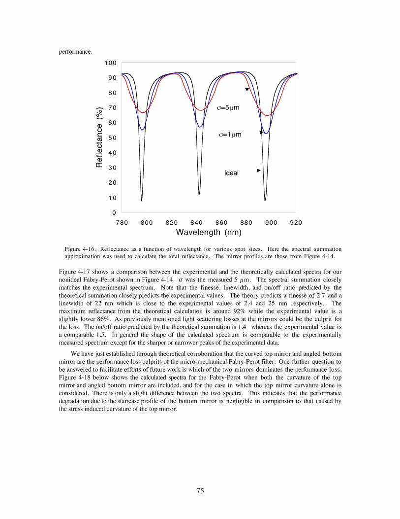
75
performance.
0
1 0
2 0
3 0
4 0
5 0
6 0
7 0
8 0
9 0
100
780 800 820 840 860 880 900 920
Wavelength (nm)
Ref
lect
ance
(%
)
Ideal
s=1mm
s=5mm
Figure 4-16. Reflectance as a function of wavelength for various spot sizes. Here the spectral summationapproximation was used to calculate the total reflectance. The mirror profiles are those from Figure 4-14.
Figure 4-17 shows a comparison between the experimental and the theoretically calculated spectra for ournonideal Fabry-Perot shown in Figure 4-14. s was the measured 5 µm. The spectral summation closelymatches the experimental spectrum. Note that the finesse, linewidth, and on/off ratio predicted by thetheoretical summation closely predicts the experimental values. The theory predicts a finesse of 2.7 and alinewidth of 22 nm which is close to the experimental values of 2.4 and 25 nm respectively. Themaximum reflectance from the theoretical calculation is around 92% while the experimental value is aslightly lower 86%. As previously mentioned light scattering losses at the mirrors could be the culprit forthe loss. The on/off ratio predicted by the theoretical summation is 1.4 whereas the experimental value isa comparable 1.5. In general the shape of the calculated spectrum is comparable to the experimentallymeasured spectrum except for the sharper or narrower peaks of the experimental data.
We have just established through theoretical corroboration that the curved top mirror and angled bottommirror are the performance loss culprits of the micro-mechanical Fabry-Perot filter. One further question tobe answered to facilitate efforts of future work is which of the two mirrors dominates the performance loss.Figure 4-18 below shows the calculated spectra for the Fabry-Perot when both the curvature of the topmirror and angled bottom mirror are included, and for the case in which the top mirror curvature alone isconsidered. There is only a slight difference between the two spectra. This indicates that the performancedegradation due to the staircase profile of the bottom mirror is negligible in comparison to that caused bythe stress induced curvature of the top mirror.
76
0
1 0
2 0
3 0
4 0
5 0
6 0
7 0
8 0
9 0
100
780 800 820 840 860 880 900 920
Wavelength (nm)
Ref
lect
ance
(%
)
Theory (Flat Parallel Mirrors)
Theory (Curved Top and Angled Bottom Mirror)
Experiment
Figure 4-17. Experimental and theoretical spectra for the 101 µm long cantilever. The non ideal FabryPerot theoretical spectrum was calculated using the summation approximation.
Figure 4-19 shows the wavelength tuning behavior of one cavity mode (8 wavelengths or m = 16) as afunction of applied voltage. The diamond data points are the measured data points. The dashed linesrepresents the quadratic approximation of the resonant wavelength using :
le
e
Vm
n h hEh
V
hh
LSiO ox coo
oxco
ox
rox
( ) = + -
+é
ëê
ù
ûú
ì
í
ïï
î
ïï
ü
ý
ïï
þ
ïï
2 3
42 3
2
24
(4-4)
The solid line represents the numerical solution.
Regarding the experimental data, the reflectance minima or transmission peak varies quadratically withvoltage. Beyond 53 volts the cantilever snaps down into contact with the nickel due to the thresholdvoltage effect. The wavelength tuning range of this structure is 120 nm with 0-53 volts. As predicted bythe theory, the wavelength tuning sensitivity of the more flexible 101 µm long cantilever is higher than the30 µm long cantilever analyzed with the Ti:Sapphire laser (40 nm: 40 V). Analytic solutions are plottedfor oxide elasticity moduli of 7.3 ´ 1010 Nm2 and 5.0 ´ 1010 Nm2. As shown by the theoretical curves thereported value of 7.3 ´ 1010 Nm2 for fused silica results in an underestimate in the wavelength shift. Areduction of the elasticity modulus to 5.0 ´ 1010 Nm2 results in closer agreement with the measured data.
77
5 0
5 5
6 0
6 5
7 0
7 5
8 0
8 5
9 0
9 5
100
780 800 820 840 860 880 900 920
Wavelength (nm)
Ref
lect
ance
(%
)
Theory (Curved Top and Flat Bottom Mirrors)
Experiment
Theory (Curved Top and Angled Bottom Mirrors)
Figure 4-18. Experimental and theoretical spectra for the 101 µm long cantilever. The theoretical spectrawere calculated using the weighted spectral summation. The dashed curves represent the theoretical spectra.The finesse degradation due to the top mirror curvature is dominant.
The experimental results presented in the next section for the time resolved response characteristics alsosuggest an elasticity modulus of 5.0 ´ 1010 Nm2. It is reasonable to expect a smaller elasticity for ourgrown wet oxides in comparison to fused silica or dry oxide. Wet oxides exhibit lower densities than dryoxide or fused silica. A lower density results in a smaller number of springs per unit volume and a smallerelectronic binding force between atoms (decreased stiffness) . K. E. Petersen has shown in earlier work withcantilever structures a measured elasticity modulus for a wet oxide of 5.7 ´ 1010 Nm2 and 6.9 ´ 1010 Nm2
for a dry oxide [3]. He reports an accuracy of +/- 20%. Our measured value of 5.0 ´ 1010 Nm2 is withinthe bounds of his accuracy and consistent with his results. Figure 4-20 shows the behavior of the on/offratio as a function of applied voltage. The ratio increases from a value of 1.26 at 0 volts to a value of 1.5at 40 volts where it saturates. This behavior is most probably due to the lack of mirror parallelism at 0volts. At zero volts the cantilever tip is bending upward due to stress induced curvature. An increase involtage would bring the tip of the cantilever down into better parallelism with the Ni layer below providingfor a more stable optical resonator (the light beam is focused on the tip of the cantilever). Consequently,the on/off ratio is improved.
The repeatability of the filter tuning characteristic was studied. One concern was the potential changesin the shape and elasticity of the cantilevers following the application of a voltage higher than the thresholdvoltage. Beyond the threshold voltage the cantilever snaps down into full contact with the nickel/siliconsurface. The large attractive force provided by the high voltage could result in the plastic deformation of thecantilever and possibly stiction. Stiction, as mentioned earlier, is a common problem with micro-machined
78
760
780
800
820
840
860
880
900
0 1 0 2 0 3 0 4 0 5 0 6 0
Voltage (V)
Wav
elen
gth
(nm
)E=7.3X10¹⁰N/m2
E=5.0X10¹⁰N/m2
Measured
Numerical Solution
Quadratic Approx.
Figure 4-19. Minimum reflectance wavelength for one cavity mode as a function of applied DC voltage.The theoretical predictions using 5.0 X 10¹⁰ N/m2 for the oxide elasticity modulus closely match theexperimentally measured values.
structures. Stiction refers to the sticking of the cantilever to the substrate due to intersolid forces. Thesticking force is higher with increased contact area. Large contact area between two structures is providedwhen their surfaces are maximally smooth as in the case of two smooth Fabry-Perot mirrors.
Figure 4-21 illustrates the repeatability of the cantilever spectrum. A spectrum was measured at 40volts bias before the cantilever was pushed beyond the threshold voltage. A second spectrum also measuredat 40ÊV bias is shown. This spectrum was taken following 10 voltage cycles. During each cycle thecantilever was snapped down into contact with the nickel at the threshold voltage and then released duringthe reverse sweep (0 to 54 to 0 volt cycle).
As shown the spectrum is repeatable and shows no measurable wavelength shift. This suggest that thestress forces are not sufficient to plastically deform the cantilever. Some stiction was observed on thisdevice but not permanent sticking. The threshold voltage remained constant at 54 V over the 10 cycles..However, the release voltage decreased from 13 V to 5 V over the 10 cycles. The reduction in releasevoltage for the structure is believed to be due to the increased conformality of the cantilever oxide surface tothe nickel surface during the contact cycling. The increased contact surface area would result in greaterstiction forces and consequently a lower release voltage.
The effects of the continuous oscillation of the cantilever on spectral repeatability was also studied. A41ÊV DC bias in series with a 5 V peak-to-peak AC signal at 10 KHz was applied to the 101 µm long
79
1.20
1.30
1.40
1.50
1.60
0 1 0 2 0 3 0 4 0 5 0
Voltage (V)
On/
Off
Rat
io
Figure 4-20. On/Off ratio versus voltage for the cantilever Fabry-Perot.
5 0
6 0
7 0
8 0
9 0
100
780 800 820 840 860 880 900 920
Wavelength (nm)
Re
flect
ivity
(%
)
Before V>Vth
After 10 Cycles
Figure 4-21. Repeatability of the cantilever Fabry-Perot spectra before and after cycling the cantilever from0 to 54 volts and back ten times. Both spectra were measured at 40 V applied bias. Significant changes inthe spectrum were not observed.
cantilever Fabry-Perot. The signal was applied for 8 hours. Spectra were taken at 41 V before and after the8Êhour period. Figure 4-22 shows the spectra.
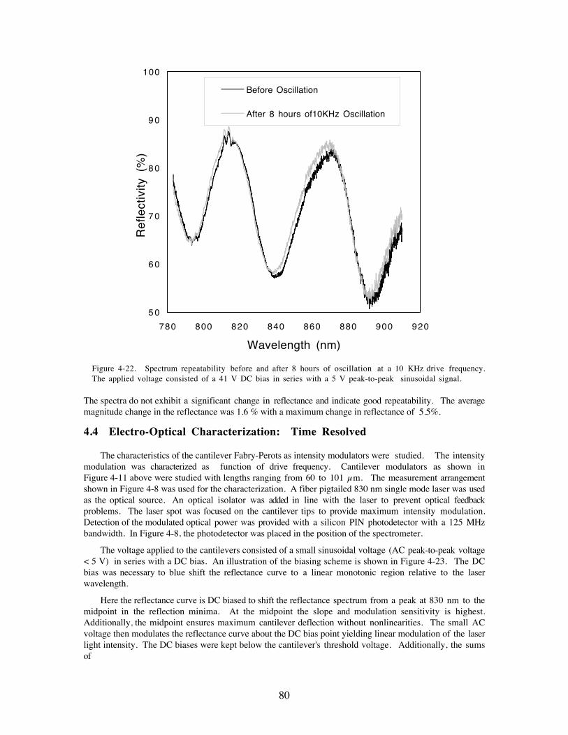
80
5 0
6 0
7 0
8 0
9 0
100
780 800 820 840 860 880 900 920
Wavelength (nm)
Re
flect
ivity
(%
)
Before Oscillation
After 8 hours of10KHz Oscillation
Figure 4-22. Spectrum repeatability before and after 8 hours of oscillation at a 10 KHz drive frequency.The applied voltage consisted of a 41 V DC bias in series with a 5 V peak-to-peak sinusoidal signal.
The spectra do not exhibit a significant change in reflectance and indicate good repeatability. The averagemagnitude change in the reflectance was 1.6 % with a maximum change in reflectance of 5.5%.
4.4 Electro-Optical Characterization: Time Resolved
The characteristics of the cantilever Fabry-Perots as intensity modulators were studied. The intensitymodulation was characterized as function of drive frequency. Cantilever modulators as shown inFigureÊ4-11 above were studied with lengths ranging from 60 to 101 µm. The measurement arrangementshown in Figure 4-8 was used for the characterization. A fiber pigtailed 830 nm single mode laser was usedas the optical source. An optical isolator was added in line with the laser to prevent optical feedbackproblems. The laser spot was focused on the cantilever tips to provide maximum intensity modulation.Detection of the modulated optical power was provided with a silicon PIN photodetector with a 125 MHzbandwidth. In Figure 4-8, the photodetector was placed in the position of the spectrometer.
The voltage applied to the cantilevers consisted of a small sinusoidal voltage (AC peak-to-peak voltage< 5 V) in series with a DC bias. An illustration of the biasing scheme is shown in Figure 4-23. The DCbias was necessary to blue shift the reflectance curve to a linear monotonic region relative to the laserwavelength.
Here the reflectance curve is DC biased to shift the reflectance spectrum from a peak at 830 nm to themidpoint in the reflection minima. At the midpoint the slope and modulation sensitivity is highest.Additionally, the midpoint ensures maximum cantilever deflection without nonlinearities. The small ACvoltage then modulates the reflectance curve about the DC bias point yielding linear modulation of the laserlight intensity. The DC biases were kept below the cantilever's threshold voltage. Additionally, the sumsof
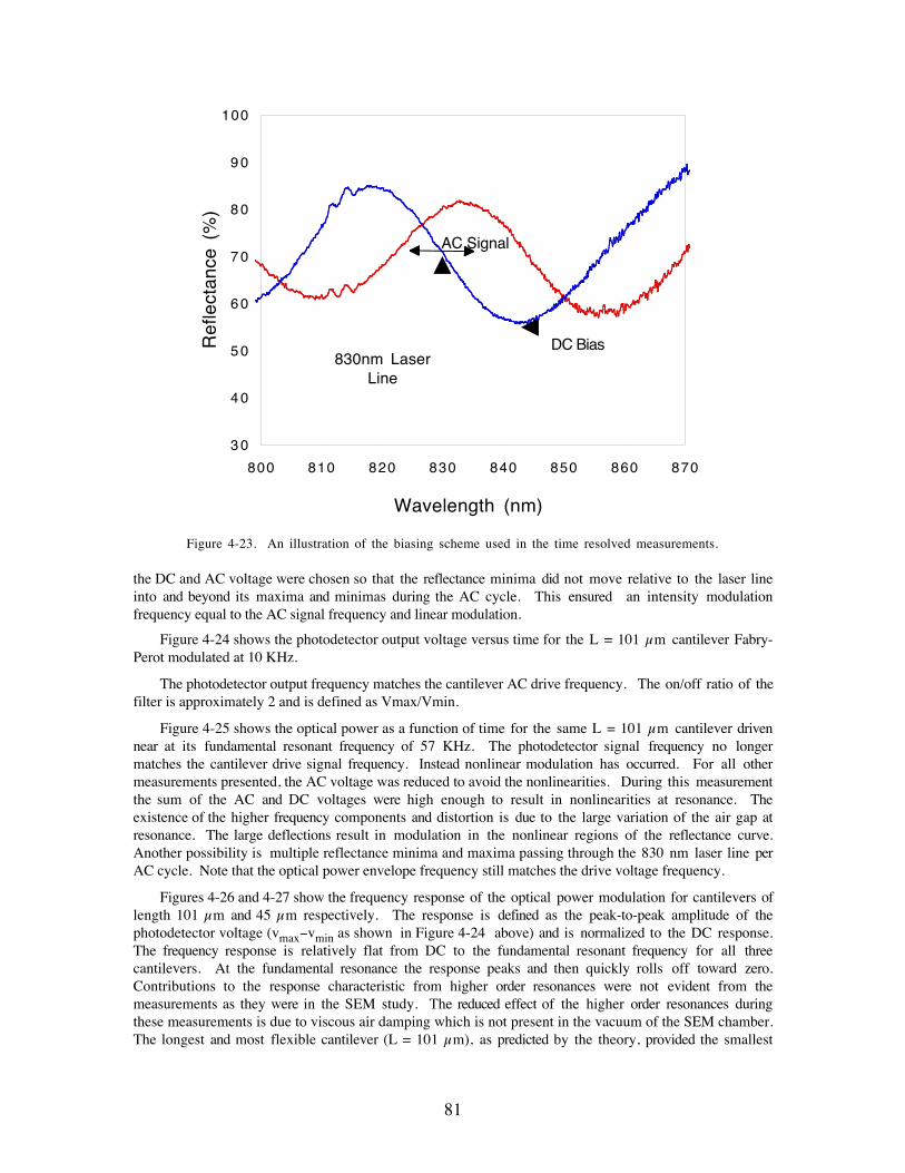
81
3 0
4 0
5 0
6 0
7 0
8 0
9 0
100
800 810 820 830 840 850 860 870
Wavelength (nm)
Ref
lect
ance
(%
)
830nm LaserLine
AC Signal
DC Bias
Figure 4-23. An illustration of the biasing scheme used in the time resolved measurements.
the DC and AC voltage were chosen so that the reflectance minima did not move relative to the laser lineinto and beyond its maxima and minimas during the AC cycle. This ensured an intensity modulationfrequency equal to the AC signal frequency and linear modulation.
Figure 4-24 shows the photodetector output voltage versus time for the L = 101 µm cantilever Fabry-Perot modulated at 10 KHz.
The photodetector output frequency matches the cantilever AC drive frequency. The on/off ratio of thefilter is approximately 2 and is defined as Vmax/Vmin.
Figure 4-25 shows the optical power as a function of time for the same L = 101 µm cantilever drivennear at its fundamental resonant frequency of 57 KHz. The photodetector signal frequency no longermatches the cantilever drive signal frequency. Instead nonlinear modulation has occurred. For all othermeasurements presented, the AC voltage was reduced to avoid the nonlinearities. During this measurementthe sum of the AC and DC voltages were high enough to result in nonlinearities at resonance. Theexistence of the higher frequency components and distortion is due to the large variation of the air gap atresonance. The large deflections result in modulation in the nonlinear regions of the reflectance curve.Another possibility is multiple reflectance minima and maxima passing through the 830 nm laser line perAC cycle. Note that the optical power envelope frequency still matches the drive voltage frequency.
Figures 4-26 and 4-27 show the frequency response of the optical power modulation for cantilevers oflength 101 µm and 45 µm respectively. The response is defined as the peak-to-peak amplitude of thephotodetector voltage (vmax-vmin as shown in Figure 4-24 above) and is normalized to the DC response.The frequency response is relatively flat from DC to the fundamental resonant frequency for all threecantilevers. At the fundamental resonance the response peaks and then quickly rolls off toward zero.Contributions to the response characteristic from higher order resonances were not evident from themeasurements as they were in the SEM study. The reduced effect of the higher order resonances duringthese measurements is due to viscous air damping which is not present in the vacuum of the SEM chamber.The longest and most flexible cantilever (L = 101 µm), as predicted by the theory, provided the smallest
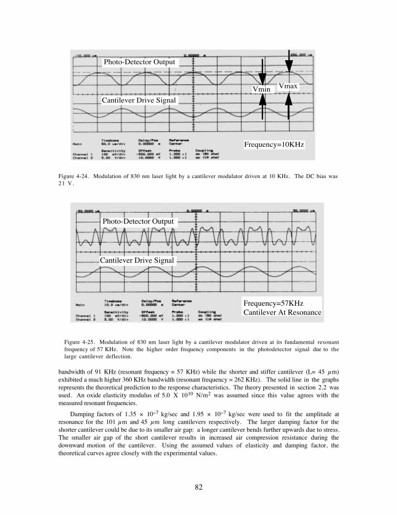
82
Cantilever Drive Signal
Photo-Detector Output
VmaxVmin
Frequency=10KHz
Figure 4-24. Modulation of 830 nm laser light by a cantilever modulator driven at 10 KHz. The DC bias was21 ÊV.
Photo-Detector Output
Cantilever Drive Signal
Frequency=57KHzCantilever At Resonance
Figure 4-25. Modulation of 830 nm laser light by a cantilever modulator driven at its fundamental resonantfrequency of 57 KHz. Note the higher order frequency components in the photodetector signal due to thelarge cantilever deflection.
bandwidth of 91 KHz (resonant frequency = 57 KHz) while the shorter and stiffer cantilever (L= 45 µm)exhibited a much higher 360 KHz bandwidth (resonant frequency = 262 KHz). The solid line in the graphsrepresents the theoretical prediction to the response characteristics. The theory presented in section 2.2 wasused. An oxide elasticity modulus of 5.0 X 10¹⁰ N/m2 was assumed since this value agrees with themeasured resonant frequencies.
Damping factors of 1.35 ´ 10-7 kg/sec and 1.95 ´ 10-7 kg/sec were used to fit the amplitude atresonance for the 101 µm and 45 µm long cantilevers respectively. The larger damping factor for theshorter cantilever could be due to its smaller air gap: a longer cantilever bends further upwards due to stress.The smaller air gap of the short cantilever results in increased air compression resistance during thedownward motion of the cantilever. Using the assumed values of elasticity and damping factor, thetheoretical curves agree closely with the experimental values.
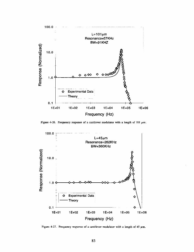
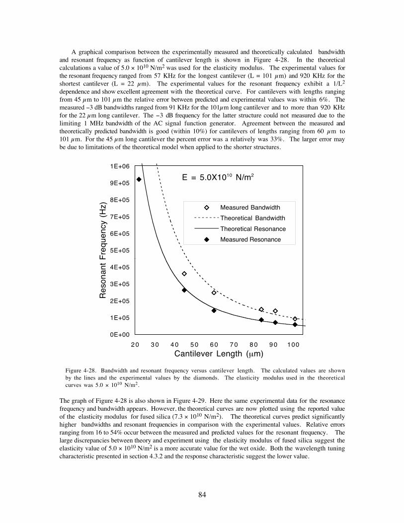
84
A graphical comparison between the experimentally measured and theoretically calculated bandwidthand resonant frequency as function of cantilever length is shown in Figure 4-28. In the theoreticalcalculations a value of 5.0 ´ 1010 N/m2 was used for the elasticity modulus. The experimental values forthe resonant frequency ranged from 57 KHz for the longest cantilever (L = 101 µm) and 920 KHz for theshortest cantilever (L = 22 µm). The experimental values for the resonant frequency exhibit a 1/L2
dependence and show excellent agreement with the theoretical curve. For cantilevers with lengths rangingfrom 45 µm to 101 µm the relative error between predicted and experimental values was within 6%. Themeasured -3 dB bandwidths ranged from 91 KHz for the 101µm long cantilever and to more than 920 KHzfor the 22 µm long cantilever. The -3 dB frequency for the latter structure could not measured due to thelimiting 1 MHz bandwidth of the AC signal function generator. Agreement between the measured andtheoretically predicted bandwidth is good (within 10%) for cantilevers of lengths ranging from 60 µm to101 µm. For the 45 µm long cantilever the percent error was a relatively was 33%. The larger error maybe due to limitations of the theoretical model when applied to the shorter structures.
0E+00
1E+05
2E+05
3E+05
4E+05
5E+05
6E+05
7E+05
8E+05
9E+05
1E+06
2 0 3 0 4 0 5 0 6 0 7 0 8 0 9 0 100
Cantilever Length (mm)
Res
onan
t F
requ
ency
(H
z) Measured Bandwidth
Theoretical Bandwidth
Theoretical Resonance
Measured Resonance
E = 5.0X10¹⁰ N/m2
Figure 4-28. Bandwidth and resonant frequency versus cantilever length. The calculated values are shownby the lines and the experimental values by the diamonds. The elasticity modulus used in the theoreticalcurves was 5.0 ´ 1010 N/m2.
The graph of Figure 4-28 is also shown in Figure 4-29. Here the same experimental data for the resonancefrequency and bandwidth appears. However, the theoretical curves are now plotted using the reported valueof the elasticity modulus for fused silica (7.3 ´ 1010 N/m2). The theoretical curves predict significantlyhigher bandwidths and resonant frequencies in comparison with the experimental values. Relative errorsranging from 16 to 54% occur between the measured and predicted values for the resonant frequency. Thelarge discrepancies between theory and experiment using the elasticity modulus of fused silica suggest theelasticity value of 5.0 ´ 1010 N/m2 is a more accurate value for the wet oxide. Both the wavelength tuningcharacteristic presented in section 4.3.2 and the response characteristic suggest the lower value.
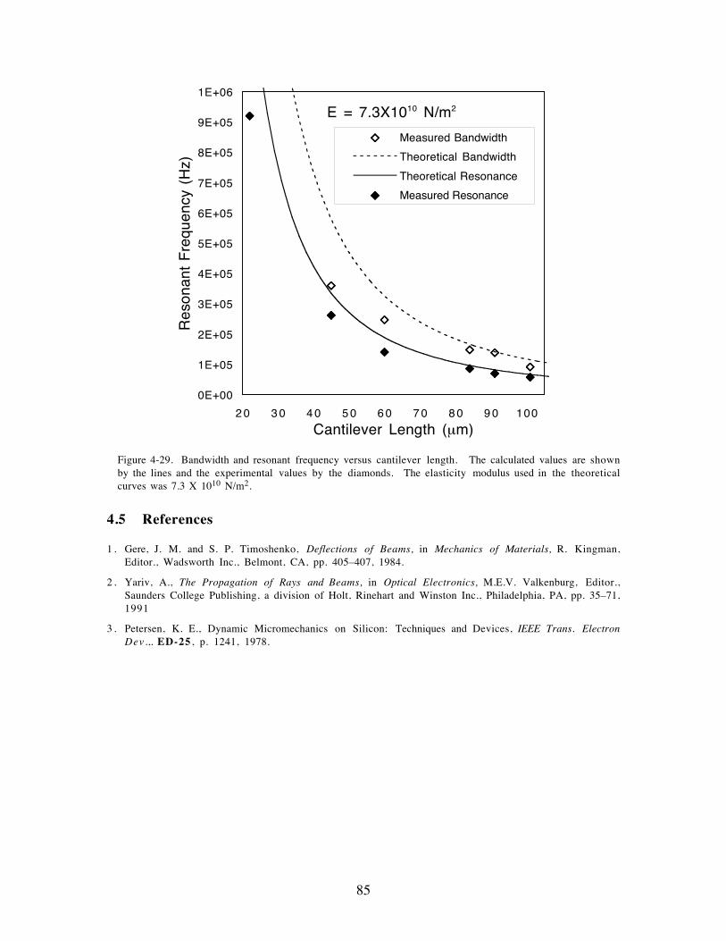
85
0E+00
1E+05
2E+05
3E+05
4E+05
5E+05
6E+05
7E+05
8E+05
9E+05
1E+06
2 0 3 0 4 0 5 0 6 0 7 0 8 0 9 0 100
Cantilever Length (mm)
Res
onan
t F
requ
ency
(H
z)
Measured Bandwidth
Theoretical Bandwidth
Theoretical Resonance
Measured Resonance
E = 7.3X10¹⁰ N/m2
Figure 4-29. Bandwidth and resonant frequency versus cantilever length. The calculated values are shownby the lines and the experimental values by the diamonds. The elasticity modulus used in the theoreticalcurves was 7.3 X 10¹⁰ N/m2.
4.5 References
1 . Gere, J. M. and S. P. Timoshenko, Deflections of Beams, in Mechanics of Materials, R. Kingman,Editor., Wadsworth Inc., Belmont, CA, pp. 405Ð407, 1984.
2 . Yariv, A., The Propagation of Rays and Beams, in Optical Electronics, M.E.V. Valkenburg, Editor.,Saunders College Publishing, a division of Holt, Rinehart and Winston Inc., Philadelphia, PA, pp. 35Ð71,1991
3 . Petersen, K. E., Dynamic Micromechanics on Silicon: Techniques and Devices, IEEE Trans. ElectronDev .,. ED-25 , p. 1241, 1978.


87
V. Conclusion
5.1 Summary of the Study: Major Issues
In this work, we have demonstrated a novel single mask level self-aligned process for fabricating micro-mechanical Fabry-Perot filters in (111) Si. We have used this process to fabricate arrays of Fabry-Perotoptical filters with a movable cantilever top mirror and a silicon based bottom mirror. Our fabricationprocess requires only one grown or deposited layer to form the movable mirror, while the substrate materialprovides for both the sacrificial layer and the bottom mirror. The structure utilizes metallic coatings toprovide for the high reflectivity mirrors. The silicon based Fabry-Perot filter can be integrated with lowcost silicon-based photodetectors and electronic circuits.
In chapter two we presented a theoretical analysis describing the movement of the cantilever as afunction of applied bias and the corresponding optical spectra. The wavelength-voltage tuning characteristicwas shown to be parabolic for low voltages. It was shown that small air gap, long length cantilever Fabry-Perots provide the highest wavelength tuning range and highest sensitivity to voltage. Hysteresis in thetuning characteristic was also predicted when the applied voltage was driven past the threshold voltage, Vth.Hysteresis is not present for voltages below Vth. The theory also predicted tradeoffs: modulator bandwidthfor wavelength tuning sensitivity and transmittance for finesse. Numerical calculations showed that 175nm of wavelength tuning range is provided with a CMOS compatible 4.75 V of applied bias, using a 1µm air gap, 100 µm long Fabry-Perot with both mirrors gold coated. The finesse of the structure with 40nm of gold thickness was calculated to be 30 with 181Ênm of free spectral range.
The details and results of our modulator fabrication process were presented in chapter 3. The processuses only one grown or deposited layer (silicon dioxide or silicon nitride) to provide the cantilever material.A single mask was used to define the cantilever structure and the electrical isolation. The sacrificial layerand lower mirror material are provided by a (111) silicon substrate. The formation of the air gap under thecantilever relies on a combination of reactive ion etching and KOH anisotropic etching on the (111) siliconsubstrate. Electrical isolation between mirrors was provided by KOH undercut eaves around the perimeterof the cantilever well and around a hexagonal isolation trench. Gold was the choice of metal for themirrors due to its high reflectivity and inertness to oxidation. Gold metallization of the cantilever wascarried out using thermal evaporation. Metallization of the silicon based bottom mirror was carried outusing selective nickel electroplating. The Ni electroplating was successful for structures with air gapslarger than 1 µm. Nickel electroplating can be followed by substitutional gold electroplating to providehigher finesse structures.
Several sources of Fabry-Perot performance degradation were observed during the fabrication. Thesmoothness and planarity of the silicon based bottom mirror was shown to be highly sensitive to thealignment of the wafer surface normal with the (111) direction (the staircase effect). Bottom mirror surfaceheight deviations ranging from 388 � to 1700 � were observed across the 20 µm width of the cantilevers.The smoothness and planarity was also shown to be affected by surface defects in the wafer (the source ofthe defects is probably the wafer sawing and polishing). The formation of pits in the silicon during theKOH etching was commonly observed especially in the case of short cavity Fabry-Perots. Thesedegradations can be reduced with tighter wafer tolerances.
Silicon dioxide and silicon nitride were presented as good candidates for the cantilever and KOHmasking material. In this study we used thermally grown silicon dioxide. A problem in using thermaloxide is the large thermal stress between the oxide and the silicon due to the high growth temperatures andlarge difference in thermal coefficients of expansion. The stress results in an upward curvature of thecantilever. This curvature results in loss of parallelism between the top and bottom mirrors andconsequently a lower finesse structure. Replacement of the thermal oxide layer with a silicon nitride layerin future devices should remedy this problem entirely since silicon nitride's thermal expansion coefficientclosely matches that of silicon.
Another problem is the rough electroplating of the silicon in the case of short cavity (on the order of 1
88
µm) Fabry-Perots. Small air gap Fabry-Perots are attractive since they provide high wavelength sensitivityto voltage. The rough plating is believed to be due to slow plating solution and byproduct transport in thetight and restrictive space under the cantilever. The roughness could be potentially improved by morerigorous solution agitation (higher rpm stirbar, ultrasonic agitation, etc.) and by improving the surfacewetting property of the plating solution .
The measured electro-mechanical and electro-optical behavior of the cantilever modulators was presentedin chapter 4. The motion and electrical isolation of a cantilever modulator under bias was studied in anSEM. Qualitative results from the SEM study showed agreement with the theory. Electrical isolationbetween the mirrors was confirmed using voltage contrast SEM. The predicted hysteretic behavior in themotion of the cantilever was also observed. However, the hysteresis was experimentally shown to beavoidable if the voltage is maintained below the threshold voltage.
The spectral tuning characteristics of the cantilevers Fabry-Perots were measured in the 700 to 900Ênmwavelength range for a 101 µm long cantilever. Agreement between the theoretically predicted andmeasured spectra required the modification of the optical theory to account for the stress induced curvature ofthe cantilever beam and the angular misalignment of the bottom mirror. The wavelength tuningcharacteristics indicated a blue shift of the wavelength with increasing voltage. The wavelength tuningcharacteristic was shown to be quadratically dependent on voltage. The theoretically calculated and measuredtuning characteristic were in agreement provided that a wet oxide elasticity modulus of 5.0Ê´ 1010 N/m2 isused. This is in agreement with Petersen's measurements which indicated a lower elasticity modulus forwet oxides (E = 5.7Ê´ 1010 N/m2 +/- 20%) in comparison to that of dry oxides (EÊ= 6.9Ê´ 1010 N/m2
+/- 20%) or fused silica (E = 7.3Ê´ 1010 N/m2).
The frequency response was measured for structures with cantilevers lengths ranging from 22 µm to101 µm. The theoretically calculated and measured frequency response were in agreement provided thatagain a wet oxide elasticity modulus of 5.0Ê´ 1010 N/m2 is used. The modulation bandwidths of thestructures ranged from 91 KHz for the 101 µm long cantilever and greater than 920 KHz for the stiffest 22µm long cantilever. The bandwidth and resonant frequency of the structures exhibited the 1/L2 dependencein agreement with the theory. A tradeoff between modulation bandwidth and on/off ratio was observedexperimentally and is consistent with theoretical calculations.
5.2 Micro-Mechanical Fabry-Perot Performance Comparison
Table 5-1 provides a comparison between the performance of our 101 µm long cantilever Fabry-Perotand Cornell's DBR Fabry-Perot which is also formed on a silicon substrate[1]. The table also includestheoretically predicted performance characteristics for our structure that are based on expected improvementsin mirror quality on future devices.
Column 1 in Table 5-1 lists the tuning sensitivities of the devices. Tuning sensitivity is defined asthe required voltage to obtain a transmission wavelength shift. Our measured device exhibits a tuningsensitivity of almost twice that of Cornell's reported structure: 120 nm: 53 V versus their 60 nm: 65 V.Our larger tuning sensitivity occurs even though their device has a much smaller air gap than our structure,3.0 µm versus our 6.27 µm. For a given voltage the electrostatic force present in their structure is 4 timesthat of ours (the electrostatic force per unit area is proportional to 1/Air Gap2). The low sensitivity of theirdevice is probably due to the many stiff DBR layers in the movable mirror structure and the movement oftheir top mirror through more difficult stretching instead of bending like our cantilever structure. Incomparing the spectral filtering quality of the micro-mechanical Fabry-Perots finesse is used as the figure ofmerit. Cornell's DBR structure exhibits a superior finesse of 35 in comparison to our structures 2.4. Inlight of the great importance of finesse as a figure of merit for the Fabry-Perot, Cornell's structure iscurrently better performance wise.
89
Table 5-1. Micro-Mechanical Fabry-Perot Performance Comparison
Tuning
Sensitivity
Finesse FSR Air
Gap
Band-
width
Number of
LayersRequired
CUB Measured
Au-Ni
120nm:
53V
2.4 60nm 6.27µm 91 KHz 3
CUB Theory
Au-Ni
120nm:
53V
13 60nm 6.27µm 94KHz 4
CUB
Theory
Au-Au
175nm:
5V
30 181nm 1µm 94KHz 4
Cornell's DBR-DBR
60nm:
65V
35 375nm
(Calculated)
3µm ? 19
However our device deserves consideration for future research and development. A major advantage of ourstructure is its simple fabrication process. The fabrication process for our structure requires only 4 totaldeposited layers including the metallization whereas Cornell's structure requires 19 layers. Consequentlyour structure is easier to fabricate and may be more integratable with other devices. Furthermore, thetheoretical predictions suggest that the finesse of our structure can be competitive with Cornell's providedthat the mirror flatness and parallelism of our Fabry-Perot are improved. As previously mentioned, the lowfinesse of our structure is attributable to the curvature of the cantilever top mirror and the misalignment ofthe bottom mirror. The replacement of the thermal oxide with either a low temperature oxide or siliconnitride should result in lower stress and a much straighter cantilever. Tighter tolerances on the waferalignment will reduce the misalignment of the bottom mirror. With these improvements in place, thetheory predicts a more competitive finesse of 13 for our structure with a gold top mirror and nickel bottommirror. The finesse of 13 of course is for an ideal structure and represents an upper bound for the achievablefinesse. However we can go one step further and substitutionally replace the nickel on the lower mirrorwith the higher reflectivity gold. This improvement increases the finesse of our structure to 30 which iscomparable and competitive to Cornell's 35. Furthermore, by reducing the air gap of our structure to 1 µma CMOS compatible 5 V can provide 175 nm of tuning range.
5.3 References
1 . Tran, A. T. T. D., et al., Surface Micromachined Fabry-Perot Tunable Filter, Photonics Tech. Ltrs., 8(3),pp. 393Ð395, 1996.

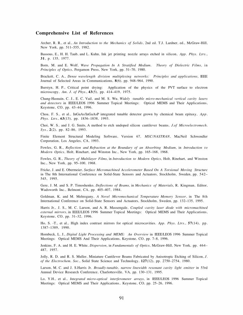
91
Comprehensive List of References
Archer, R. R., et al., An Introduction to the Mechanics of Solids, 2nd ed. T.J. Lardner, ed., McGraw-Hill,New York, pp. 511Ð555, 1982.
Bassous, E., H. H. Taub, and L. Kuhn, Ink jet printing nozzle arrays etched in silicon, App. Phys. Ltrs.,31 , p. 135, 1977.
Born, M. and E. Wolf, Wave Propagation In A Stratified Medium. Theory of Dielectric Films, inPrinciples of Optics, Pergamon Press, New York, pp. 51Ð70, 1980.
Brackett, C. A., Dense wavelength division multiplexing networks: Principles and applications, IEEEJournal of Selected Areas in Communications, 8(6), pp. 948Ð964, 1990.
Burstyn, H. P., Critical point drying: Application of the physics of the PVT surface to electronmicroscopy, Am. J. of Phys., 43(5), pp. 414Ð419, 1975.
Chang-Hasnain, C. J., E. C. Vail, and M. S. Wu, Widely -tunable micro-mechanical vertical cavity lasersand detectors in IEEE/LEOS 1996 Summer Topical Meetings: Optical MEMS and Their Applications,Keystone, CO, pp. 43Ð44, 1996.
Choa, F. S., et al., InGaAs/InGaAsP integrated tunable detector grown by chemical beam epitaxy, App.Phys. Ltrs., 63(13), pp. 1836Ð1838, 1993.
Choi, W. S.. and J. G. Smits, A method to etch undoped silicon cantilever beams, J.of Microelectromech.Sys ., 2(2), pp. 82Ð86, 1993.
Finite Element Structural Modeling Software, Version 67, MSC/NASTRAN, MacNeil SchwendlerCorporation, Los Angeles, CA, 1993.
Fowles, G. R., Reflection and Refraction at the Boundary of an Absorbing Medium, in Introduction toModern Optics, Holt, Rinehart, and Winston Inc., New York, pp. 165Ð168, 1968.
Fowles, G. R., Theory of Multilayer Films, in Introduction to Modern Optics, Holt, Rinehart, and WinstonInc., New York, pp. 95Ð100, 1968.
Fricke, J. and E. Obermeier, Surface Micromachined Accelerometer Based On A Torsional Moving Structurein The 8th International Conference on Solid-State Sensors and Actuators, Stockholm, Sweden, pp. 542Ð545, 1995.
Gere, J. M. and S. P. Timoshenko, Deflections of Beams, in Mechanics of Materials, R. Kingman, Editor,Wadsworth Inc., Belmont, CA, pp. 405Ð407, 1984.
Goldman, K. and M. Mehregany, A Novel Micromechanical Temperature Memory Sensor, in The 8thInternational Conference on Solid-State Sensors and Actuators, Stockholm, Sweden, pp. 132Ð135, 1995.
Harris Jr., J. S., M. C. Larson, and A. R. Massengale, Coupled -cavity laser diode with micromachinedexternal mirrors, in IEEE/LEOS 1996 Summer Topical Meetings: Optical MEMS and Their Applications,Keystone, CO, pp. 31Ð32, 1996.
Ho, S. -T., et al., High index contrast mirrors for optical microcavities. App. Phys. Ltrs., 57(14), pp.1387Ð1389, 1990.
Hornbeck, L. J., Digital Light Processing and MEMS: An Overview in IEEE/LEOS 1996 Summer TopicalMeetings: Optical MEMS And Their Applications, Keystone, CO, pp. 7Ð8, 1996.
Jenkins, F. A. and H. E. White, Dispersion, in Fundamentals of Optics, McGraw-Hill, New York, pp. 464Ð487, 1957.
Jolly, R. D. and R. S. Muller, Miniature Cantilever Beams Fabricated by Anisotropic Etching of Silicon, J.of the Electrochem. Soc., Solid State Science and Technology, 127(12), pp. 2750Ð2754, 1980.
Larson, M. C. and J. S.Harris Jr. Broadly-tunable, narrow linewidth resonant cavity light emitter in 53rdAnnual Device Research Conference, Charlottesville, VA, pp. 130Ð131, 1995.
Lo, Y.H., et al., Integrated micro-optical interferometer arrays, in IEEE/LEOS 1996 Summer TopicalMeetings: Optical MEMS and Their Applications.. Keystone, CO, pp. 25Ð26, 1996.
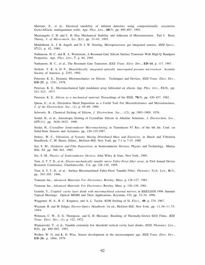
92
Martinet, E., et al., Electrical tunability of infrared detectors using compositionally assymetricGaAs/AlGaAs multiquantum wells, App. Phys. Ltrs.,. 60(7), pp. 895Ð897, 1992.
Mastrangelo, C. H. and C. H. Hsu, Mechanical Stability and Adhesion of Microstructures: Part I: BasicTheory, J. of Micro-mech. Sys., 2(1), pp. 33Ð43, 1993.
Middelhoek, S., J. B. Angell, and D. J. W. Noorlag, Microprocessors get integrated sensors, IEEE Spect.,17(2), p. 42, 1980.
Nathanson, H. C. and R. A. Wickstrom, A Resonant-Gate Silicon Surface Transistor With High-Q BandpassProperties, App. Phys. Ltrs., 7, p. 84, 1965.
Nathanson, H. C., et al., The Resonant Gate Transistor, IEEE Trans. Elect. Dev.,. ED-14, p. 117, 1967.
Neikirk, Y. K. A. D. P., Monolithically integrated optically interrogated pressure microsensor. AcousticSociety of America, p. 2353, 1992.
Petersen, K. E., Dynamic Micromechanics on Silicon: Techniques and Devices, IEEE Trans. Elect. Dev.,ED-25 , p. 1241, 1978.
Petersen, K. E., Micromechanical light modulator array fabricated on silicon, App. Phys. Ltrs., 31 (8), pp.521Ð523, 1977.
Petersen, K. E., Silicon as a mechanical material, Proceedings of the IEEE, 70(5), pp. 420Ð457, 1982.
Queau, E., et al., Electroless Metal Deposition as a Useful Tool For Microelectronics and Microstructures,J. of the Electrochem. Soc., (1), p. 65Ð69, 1994.
Schwartz, B., Chemical Etching of Silicon, J. Electrochem. Soc.,. (12), pp.Ê1903Ð1909, 1976.
Seidal, H., et al., Anisotropic Etching of Crystalline Silicon in Alkaline Solutions, J. Electrochem. Soc.,137(11), pp. 3626Ð3632, 1990.
Seidal, H., Crystalline Semiconductor Micromachining, in Transducers '87 Rec. of the 4th Int. Conf. onSolid-State Sensors and Actuators, pp. 120Ð125,1987.
Stokey, W. F., Vibrations of Systems Having Distributed Mass and Elasticity, in Shock and VibrationHandbook, C. M. Harris, Editor., McGraw-Hill, New York. pp. 7-1 to 7-15, 1988
Sze, S. M., Oxidation and Film Deposition, in Semiconductor Devices: Physics and Technology, MurrayHill, NJ, pp. 360Ð362, 1985.
Sze, S. M., Physics of Semiconductor Devices, John Wiley & Sons, NewÊYork, 1969.
Tran, A. T. T. D., et al., Electro-mechanically tunable micro Fabry-Perot filter array, in 53rd Annual DeviceResearch Conference, Charlottesville, VA, pp.Ê128Ð129, 1995.
Tran, A. T. T. D., et al., Surface Micromachined Fabry-Perot Tunable Filter, Photonics Tech. Ltrs., 8(3),pp. 393Ð395, 1996.
Transene Inc., Advanced Materials For Electronics, Rowley, Mass. p.Ê126Ð127, 1981.
Transene Inc., Advanced Materials For Electronics, Rowley. Mass. p. 138Ð139, 1981.
Uenishi, Y., Coupled -cavity laser diode with micromachined external mirrors, in IEEE/LEOS 1996 SummerTopical Meetings: Optical MEMS and Their Applications, Keystone, CO, pp. 33Ð34, 1996.
Waggener, H. A., R .C. Kragness, and A. L. Taylor, KOH Etching of Si, Elect.,. 40, p. 274, 1967.
Waynant, R. and M. Ediger, Electro-Optics Handbook, 1st ed., McGraw-Hill, New York, pp. 11.56Ð11.75,1994.
Wilmsen, C. W., E. G. Thompson, and G. H. Meissner, Buckling of Thermally-Grown SiO2 Films, IEEETrans. Elect. Dev., (1), p. 122, 1972.
Wipiejewski, T., et al., Tunable extremely low threshold vertical cavity laser diodes, IEEE Photonics Ltrs.,5(8), pp. 889Ð892, 1993.
Wolber, W. G. and K. D. Wise, Sensor development in the microcomputer age, IEEE Trans. Elect. Dev.,ED-26 , p. 1864, 1979.
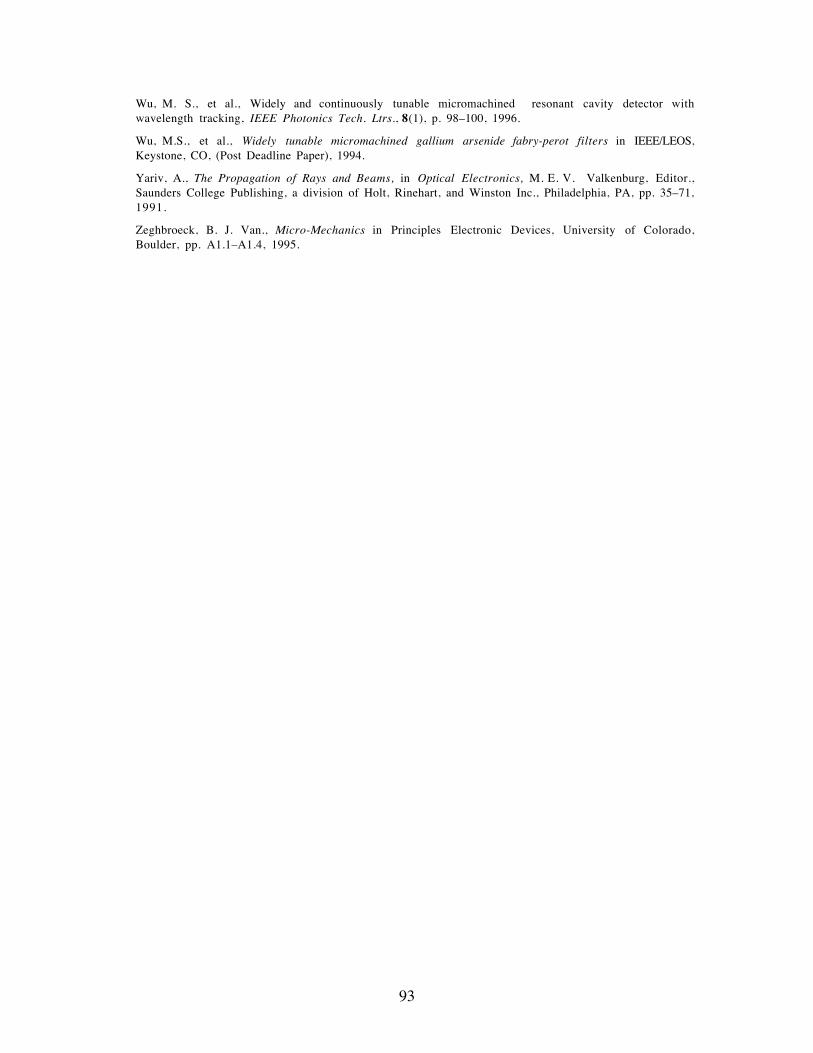
93
Wu, M. S., et al., Widely and continuously tunable micromachined resonant cavity detector withwavelength tracking, IEEE Photonics Tech. Ltrs., 8(1), p. 98Ð100, 1996.
Wu, M.S., et al., Widely tunable micromachined gallium arsenide fabry-perot filters in IEEE/LEOS,Keystone, CO, (Post Deadline Paper), 1994.
Yariv, A., The Propagation of Rays and Beams, in Optical Electronics, M.ÊE.ÊV. Valkenburg, Editor.,Saunders College Publishing, a division of Holt, Rinehart, and Winston Inc., Philadelphia, PA, pp. 35Ð71,1991.
Zeghbroeck, B. J. Van., Micro-Mechanics in Principles Electronic Devices, University of Colorado,Boulder, pp. A1.1ÐA1.4, 1995.

REPORT DOCUMENTATION PAGE Form ApprovedOMB No. 0704-0188
Public reporting burden for this collection of information is estimated to average 1 hour per response, including the time for reviewing instructions, searching existing data sources,gathering and maintaining the data needed, and completing and reviewing the collection of information. Send comments regarding this burden estimate or any other aspect of thiscollection of information, including suggestions for reducing this burden, to Washington Headquarters Services, Directorate for Information Operations and Reports, 1215 JeffersonDavis Highway, Suite 1204, Arlington, VA 22202-4302, and to the Office of Management and Budget, Paperwork Reduction Project (0704-0188), Washington, DC 20503.
1. AGENCY USE ONLY (Leave blank) 2. REPORT DATE
September 19973. REPORT TYPE AND DATES COVERED
Technical Paper4. TITLE AND SUBTITLE
Micro-Mechanical Voltage Tunable Fabry-Perot Filters Formed in (111)Silicon
5. FUNDING NUMBERS
WU 274-00-97-01
6. AUTHOR(S)
James D. Patterson
7. PERFORMING ORGANIZATION NAME(S) AND ADDRESS(ES)
NASA Langley Research CenterHampton, VA 23681-2199
8. PERFORMING ORGANIZATIONREPORT NUMBER
L-17646
9. SPONSORING/MONITORING AGENCY NAME(S) AND ADDRESS(ES)
National Aeronautics and Space AdministrationWashington, DC 20546-0001
10. SPONSORING/MONITORINGAGENCY REPORT NUMBER
NASA TP-3702
11. SUPPLEMENTARY NOTES
The information in this report was offered as a thesis in partial fulfillment of the requirements for the Degree ofDoctor of Philosophy in Electrical Engineering, University of Colorado, Boulder, Colorado.
12a. DISTRIBUTION/AVAILABILITY STATEMENT
Unclassified-UnlimitedSubject Category 33Availability: NASA CASI (301) 621-0390
12b. DISTRIBUTION CODE
13. ABSTRACT (Maximum 200 words)
The MEMS (Micro-Electro-Mechanical-Systems) technology is quickly evolving as a viable means to combinemicro-mechanical and micro-optical elements on the same chip. One MEMS technology that has recently gainedattention by the research community is the micro-mechanical Fabry-Perot optical filter. A MEMS based Fabry-Perot consists of a vertically integrated structure composed of two mirrors separated by an air gap. Wavelengthtuning is achieved by applying a bias between the two mirrors resulting in an attractive electrostatic force whichpulls the mirrors closer. In this work, we present a new micro-mechanical Fabry-Perot structure which is simpleto fabricate and is integratable with low cost silicon photodetectors and transistors. The structure consists of amovable gold coated oxide cantilever for the top mirror and a stationary Au/Ni plated silicon bottom mirror. Thefabrication process is single mask level, self aligned, and requires only one grown or deposited layer.Undercutting of the oxide cantilever is carried out by a combination of RIE and anisotropic KOH etching of the(111) silicon substrate. Metallization of the mirrors is provided by thermal evaporation and electroplating.The optical and electrical characteristics of the fabricated devices were studied and show promissing results . Awavelength shift of 120nm with 53V applied bias was demonstrated by one device.
14. SUBJECT TERMS
Micro-Electro-Mechanical Systems (MEMS) , Fabry-Perot Filters,15. NUMBER OF PAGES
107
Silicon Micro-Machining 16. PRICE CODE
A0617. SECURITY CLASSIFICATION
OF REPORT
Unclassified
18. SECURITY CLASSIFICATIONOF THIS PAGE
Unclassified
19. SECURITY CLASSIFICATION OF ABSTRACT
Unclassified
20. LIMITATION OF ABSTRACT
NSN 7540-01-280-5500 Standard Form 298 (Rev. 2-89)Prescribed by ANSI Std. Z-39-18298-102