meptec advisory board semiconductor industry outlook 2016meptec.org/resources/mtrpt spring 2016 4...
TRANSCRIPT
SEMICONDUCTOR INDUSTRY OUTLOOK
2016page 12
MEPTEC ADVISORY BOARD
A Quarterly Publication of The Microelectronics Packaging & Test Engineering Council Volume 20, Number 1
SPRING 2011 MEPTEC Report 3
-Corp.INSIDE THIS ISSUE
MEPTEC MEMBER COMPANY PROFILEFor more than 35 years, Promex has been known for the high caliber of its engineering staff grounded in materials science, chemistry, metallurgy, polymer science, chemical engineering, ceramic science and electrical engineering. page 14
SPRI
NG
201
6
Enabling the next growth wave – A new approach to enable innovative startups.3424
What is needed is a design environment that allows you to see chip, package, and board in one canvas.21
The New SiP Era – The slowdown of silicon technology scaling is accelerating the wider adoption of SiP.10
Emerging IoT Applications and the Importance of packaging and Assembly.
Package it. Visit: aseglobal.com
Innovative IC, System-in-Package, and MEMS packaging portfolio for today’s
miniaturization, mobility, and IoT needs.
Wire Bond
FlipChip
WLP2.5D& 3D
Fanout SiP
Senseit.
Moveit.
Wearit.
MEPTEC Report Vol. 20, No. 1. Published quarterly by MEPCOM LLC, 315 Savannah River Dr., Summerville, SC 29485. Copyright 2016 by MEPCOM LLC. All rights reserved. Materials may not be reproduced in whole or in part without written permission. MEPTEC Report is sent without charge to members of MEPTEC. For non-members, yearly subscriptions are available for $75 in the United States, $80US in Canada and Mexico, and $95US elsewhere. For advertising rates and information contact Gina Edwards at 408-858-5493, Fax Toll Free 1-866-424-0130.
A Quarterly Publication of The Microelectronics Packaging & Test Engineering Council Volume 20, Number 1
SPRI
NG
201
6
ON THE COVERFor this first issue of 2016, we asked several of our MEPTEC Advisory Board members to share their outlook for 2016 from their perspec-tive. They weren’t given any guidelines on what to report, and it was interesting to see that they all covered different, and thought-provoking, perspectives. Issues such as consolidation and innovation, what’s happen-ing in China, mergers and acquisitions, the continuing importance of IC packaging, and a rather provocative opinion on “why do we still need IC packages”? were covered. We hope you enjoy their thoughts!
10 ANALYSIS – IoT or connectivity everywhere means there will be lots of sensors and other components, but
many of the packages must be low cost to meet end product price targets. This puts pressure on the companies that will assemble the package. Ultimately, package choice will be deter-mined by the least expensive package that meets the needs.
E. JAN VARDAMAN AND TREVOR YANCEY TECHSEARCH INTERNATIONAL, INC.
21 TECHNOLOGY – The Semiconductor Industry is entering into a new era for System in Package being
driven by miniaturization, heterogonous integration, and high computing power requirements from applications, such as internet, mobile, cloud, and IoE. 2.5D/3D SiP provides cost effective, feature enriching, and fast time to market solutions.
HUI LIU, NATE UNGER, AND JOHN XIE INTEL CORPORATION
14 PROFILE – Promex’s specialty is integrating conven-tional SMT with IC assembly for production of com-
plex products. They offer a mix of in-house packaging and engineering services, including custom QFN and substrate design, wafer, die attach, wire bond, flip chip, multi-die and stacked die modules and encapsulation.
PROMEX INDUSTRIESMEMBER COMPANY PROFILE
DEPARTMENTS 4 Member News 9 Industry Insights
18 SMART Microsystems News28 Henkel News
32 PacTech News34 Opinion
10 MEPTEC REPORT SPRING 2016 meptec.org
developed fan-out wafer level package solutions. Laminate packages such as BGAs with wire bond or flip chip have also been introduced. Local interconnect networks (LIN) for automobiles may use SiP. For ex-ample, Atmel offers its ATA6613C that consists of two ICs in one package to support in-vehicle LIN networks.
Future Demand for SiP for IoT? TechSearch International defines SiP as a functional system or subsystem assembled into a standard footprint pack-age such as LGA, FBGA, QFN, or FO-WLP. It contains two or more dissimilar die, typically combined with other com-ponents such as passives, filters, MEMS, sensors, and/or antennas. The compo-nents are mounted together on a substrate to create a customized, highly integrated product for a given application. SiPs may utilize a combination of advanced packaging including bare die (wire bond or flip chip), wafer level packages, pre-packaged ICs such as CSPs, stacked
packages, stacked die, or any combina-tion of these. In some cases the package may be an embedded die solution. SiP formats include ball grid arrays (BGAs) and fine pitch BGAs (FBGAs) with laminate substrates, leadframe pack-ages such as QFPs and QFNs, stacked die packages, and other forms of 3D interconnect such as silicon interposers or 3D ICs. Where this is demand for increased performance in a small form factor, SiP will likely be adopted. Co-design, where the IC design, package, and board designers communicate will be important to the successful adoption of SiPs for IoT applications.
Critical Factors Cost-effect, high yielding assembly methods are also required. Both OSATs and EMS companies may benefit from the expansion of connectivity regardless of whether we call it IoT or IoE.
Conclusions IoT or connectivity everywhere
means there will be lots of sensors and other components, but many of the packages must be low cost to meet end product price targets. This puts pressure on the companies that will assemble the package. Ultimately, package choice will be determined by the least expensive package that meets the performance needs. ◆
SPRING 2016 MEPTEC REPORT 11meptec.org
/ Silicon Valley
JOEL CAMARDA [email protected] 415.290.6374
SemiOps Semiconductor Operations & Manufacturing Consulting
Get your manufacturing operations running efficiently and cost effectively!
Over 30 years experience in semiconductor manufacturing, operations exec and engineering management.
Trusted by Silicon Valley VCs to help make investments more profitable.
Consulting & Project Management Services:n Manufacturing & Operations – wafer fab through assembly-testn Supply chain & logistics management, supplier selection, negotiation, qualificationn Package & assembly process engineering: specific expertise in Au, Ag, Cu WB, wafer bumping, substrates, hi thermal appsn Production control, planning, business forecastingn Troubleshooting manufacturing operations, yield & productivity improvement
About TechSearch International
TechSearch International, Inc. was founded in Austin, Texas, in 1987 by E. Jan Vardaman as a technology licensing and consulting firm spe-cializing in the electronics industry. They are recognized around the world as a leading consulting com-pany in the field of advanced semi-conductor packaging technology. TechSearch International, Inc. is located at 4801 Spicewood Springs Rd., Suite 150, Austin, Texas 78759, USA, phone +1.512.372.8887.
ANALYSIS
Emerging IoT Applications and the Importance of Packaging and Assembly E. Jan Vardaman and Trevor Yancey TechSearch International, Inc.
GROWING DEMAND FOR CONNECTED devices and systems is commonly re-ferred to as the Internet of Things (IoT), or as Cisco likes to call it, the Internet of Everything (IoE). IoT is the increased deployment of smart devices to collect data, transmit and/or process informa-tion. It is driving new requirements for packaging and assembly. This translates into an increasing number of sensors, processors or controllers, RF devices, and even memory. Which packages best meet the needs for these emerging applications? Some companies consider multi die integration a cost-effective solution for the growing connectivity requirements. Formats include a variety of packages such as leadframe, laminate substrates, fan-out wafer level packages (FO-WLP), and other alternatives. Some of these packages fall into the category of system-in-package (SiP), while others are simply miniaturized printed circuit boards (PCBs). The greatest profits may go to the software companies that provide data collection, storage, and analysis, but this does not mean that hardware is not important. The devices used for IoT and how they are designed, assembled, and packaged, are critical to the success of the products. Revenue from services related to IoT depends upon the collection of accurate data. The cost-effective assembly of the devices and the ultimate reliability of the pack-age are important.
Component Growth in IoT A number of industrial segments are expected to benefit from the use of IoT. These segments include energy production, transportation, water treat-ment plants, and factories. Capturing information using sensors is expected to be essential in all of these areas, but the required hardware and the format for the semiconductor packages used in these
applications remain to be determined. A study by PriceWaterhouse surveyed U.S. manufacturers to determine their current activities and plans for digitized manufacturing. According to the survey, 35 percent are currently collecting and using data generated by smart sensors to enhance manufacturing/operating pro-cesses, 17 percent plan to do so in the
next three years, and another 24 percent have plans but no timeline. In addition, 34 percent of manufacturers believe that it is “extremely critical” that U.S. manu-facturers adopt an IoT strategy in their operations and 60 percent believe it is slightly or moderately critical. Much of the IoT discussion is associ-ated with machine-to-machine (M2M) applications. This would include sensors, a microcontroller to capture, process, and analyze the sensor data, possibly some type of memory to store information temporarily, and a connectivity device (typically wireless) to transmit the data. An antenna is designed in the module. Miniaturization is not typically required and therefore a standard PCB with surface mount components and pack-aged die is sufficient. In cases where a plug-and-play RF solution is desired, the design may incorporate an RF solution in a SiP. Companies including TDK have designed RF modules for these appli-cations. In addition, applications that require miniaturization may need SiP.
The SiP may be in the format of a lead-frame or a laminate package, or simply a small board with components mounted on it. Smart homes include smart light-ing, safety monitors, smoke detection, temperature control, pet care, and video entertainment. Bosch estimates that by 2020, 15 percent of all households (i.e., 230 million homes) will use some form of smart home technology. According to Philips, some smart lighting applications are expected to use SiP. Augmented reality or virtual real-ity headset require motion-tracking and orientation sensors. The design of these headsets is underway and new products are expected this year. Cost-effective solutions that make the headsets less bulky will be essential to the success of these new products. The electronic content of cars is increasing and systems that provide improved safety features are an impor-tant part of the expansion. While the connected car may still be in the distant future, many safety features are already being adopted. With the expanding mar-ket for Advanced Driver Assist Systems (ADAS) driven by government regula-tions and customer demand, the use of sensors is increasing. ADAS components include many different sensors and radar modules, as well as microcontrollers. As sensors continue to be introduced for a variety of functions, the overall sensory assimilation and control will require high-speed computing and increased use of high-speed memory. Sensors from companies such as Infineon have tra-ditionally been package din leadframe packages such as SOs, SOTs, SONs, QFPs, and TSOPs. Some of the new packages are in the form of an SiP solu-tion. Both Infineon and NXP have devel-oped SiP solutions for automotive radar. (Both NXP and Freescale independently
Ultimately, package choice will be
determined by the least expensive
package that meets the performance needs.
24 MEPTEC REPORT SPRING 2016 meptec.org SPRING 2016 MEPTEC REPORT 25meptec.org
wide variety of ball and bump pin pat-terns. You may generate regular ring and array, staggered and in-line, and irregular patterns. Rule-based patterns may be generated on a block-by-block basis, and regular patterns may be saved and repli-cated throughout the part. In the early stages of pin design, it is important to be able to define the signal, power, and ground patterns for pins of a device. But all too often these definitions are created in a spreadsheet and then man-ually transferred to the physical design. Two solutions to automating this process are provided in the OrbitIO sys-tem planner. First is to create the signal, power, and ground patterns on a pin array (bump or ball), then assign signals, power, and ground to that array. As shown in Figure 3, different patterns can be used in different parts of the design depending on requirements. The second approach is to define sig-nal, power, and ground ratios in the inter-face floorplans (see next section). As the floorplans are mapped to the pins of the device, power and ground pins are also reserved in the correct signal-to-power-to-ground ratios.
Bundling with Interfaces Typical layout tools enable the layout of signals on a signal-by-signal or pin-by-pin basis. Automatic and manual routing tools also work on a signal-by-signal
I/O Pad Creation and Optimization The OrbitIO system planner greatly simplifies I/O pad placement and align-ment. It is especially useful in a wire bond die stack where you need to align I/O pads between dies in a die stack or between side-by-side dies (see Figure 2). Pin Pattern Generation Every designer, device, and project has different pin pattern and pin assignment requirements. The OrbitIO system planner provides you with the ability to create a
package and IC design tools. The users of these tools are the respective board, pack-age, and IC designers, and changes to the interfaces are shared by exchange of the relevant files. The second is the multi-fabric design and optimization flow, which is enabled by OrbitIO™ system planner, a hierarchical “start-from-whatever-you-have” design environment. When I say hierarchical, I mean you can import an existing PCB file, place a package in it, and place several dies in the package. The net name space is preserved throughout the design hierarchy (see Figure 1). In one design canvas, you can view the PCB, package, and die, and assign and optimize pinouts in the context of the whole system. The technology, dimensions, and layer stack-up informa-tion for each device is preserved, and the net name space of each device is pre-served. You may even import dies from different technology nodes. “Start-from-whatever-you-have” means exactly what it says. You do not have to have a full layer stack-up or full constraint deck setup. You do not need a full netlist or full device library. You don’t have to have anything to get started. Any-thing you don’t have, you create on the fly. Anything you do have, you use. The user of the OrbitIO interconnect designer may be a package layout engineer, but could also be an IC designer, product engineer, or a product architect. It doesn’t take a package or board layout expert to use the OrbitIO system planner – it is intended to be lightweight, easy to get started, and easy to use.
Functionality Key functionality that enables pathway design and optimization consists of topol-ogy exploration, I/O pad creation and optimization, pin pattern generation, bun-dling with interfaces, breakout feasibility routing, and variants.
Topology Exploration Topology exploration is the defining of where each function will be designed in the system – on the chip, in the package, in the board, on an interposer, etc. The OrbitIO system planner’s unique hierar-chical architecture makes it easy to move components and functions between the die, the package, and the board so you can quickly explore different design solutions.
DESIGN
Chip/Package/Board Interface Pathway Design and Optimization
optimization environment consists of two parts. The first part includes the chip, package, and board implementation tools, namely Allegro® PCB Designer for board implementation, Cadence® SiP Layout for package implementation, and Innovus™
Implementation System for die imple-mentation. During the implementation process, minor changes to the ball array or IC bump or I/O patterns (net swaps, bump depopulation, driver swaps, bump moves, etc.) are sometimes required. Our co-design refinement flow enables these changes to be easily passed between the
routing is run, the planning results will drive an optimal routing result. All design planning results must be easily accessible in the layout environment and must drive actual layout in physical implementation tools. In this article, I will describe such an environment as provided by Cadence. To do so I will divide the description in three parts: design environment, functionality, and system integration.
Design Environment The interface pathway design and
TIME AND AGAIN, AS I MEET WITH engineers throughout the world, I find that many are still using spreadsheets for IC bump and package ball map creation, and are using drawing tools or spreadsheets for defining bond pad placement. I also find that the chip/package/board design process is still very serial, with the IC being designed first, then the package, then the board, or some variation thereof. What is needed is a design environment that enables the signal pathway design throughout the board, package, and die simultaneously and allows you to see all three design fabrics (chip, package, and board) in one canvas. This environment must support the wide range of IC and package design styles in use today – from simple single-die packages to complex packages like wire-bond stack-ups, 2.5D interposers, wafer scale packaging, and so forth. The end goal is to get the dies placed in a package, and packages placed on the board in such a way that all the signals from the board to each die in each package can be routed in a minimum amount of time on a minimum number of layers and still meet design requirements. An environment to do this must be lightweight, with simple start-up require-ments. You should not need a complete design netlist, pinout, library, constraints, or technology to get started. It should be a simple environment that doesn’t require a layout expert. A hierarchical database is needed to keep track of the various netlists and technologies. You should be able to design from whatever you have at the moment. If you have a board available, design from the board up to the chip. If you have a chip, design down through the package to the board. Whatever you don’t have, you should be able to create dynam-ically. Pin placement and optimization must be routing based so that, when final
Tom Whipple, Product Engineering Architect Cadence Design Systems
Figure 1. The top image shows the device hierarchy and the bottom image shows a graph of one net.
Figure 2. Package with three wire bond dies. On the left side, the yellow die is on top of the grey die. Another grey die is on the right. Red lines show connections between I/O drivers aligned between dies in the two stacks and the BGA.
Figure 3: BGA ball array with signal, power, and ground planning completed and with some net assignments completed.
SEMICONDUCTOR INDUSTRY OUTLOOK
2016page 12
MEPTEC ADVISORY BOARD
A Quarterly Publication of The Microelectronics Packaging & Test Engineering Council Volume 20, Number 1
SPRING 2011 MEPTEC Report 3
-Corp.INSIDE THIS ISSUE
MEPTEC MEMBER COMPANY PROFILEFor more than 35 years, Promex has been known for the high caliber of its engineering staff grounded in materials science, chemistry, metallurgy, polymer science, chemical engineering, ceramic science and electrical engineering. page 14
SPRI
NG
201
6
Enabling the next growth wave – A new approach to enable innovative startups.3424
What is needed is a design environment that allows you to see chip, package, and board in one canvas.21
The New SiP Era – The slowdown of silicon technology scaling is accelerating the wider adoption of SiP.10
Emerging IoT Applications and the Importance of packaging and Assembly.
PROFILE
14 MEPTEC REPORT SPRING 2016 meptec.org SPRING 2016 MEPTEC REPORT 15meptec.org
DESIGNING COMPLEX MEDICAL, biotech, bioscience and military products for production is a challenge. Assembly is even more demanding, as it often involves a complex series of steps to accurately locate and join components, control adhe-sive fillets, create solid interconnects, seal joints to prevent liquid leakage, etc. Extensive process engineering experi-ence with electronic and microelectronic assembly and processes is a necessity. To meet these challenges and bring products from proof of concept to full production in record time, companies turn to electron-ic manufacturing services (EMS) provid-ers such as Promex Industries Inc. Promex’s specialty is integrating conventional SMT with IC assembly for production of complex products. The company offers a mix of in-house packag-ing and engineering services, including custom QFN and substrate design, wafer
Promex Engineering, Mixed Assembly, IC Packaging Services Accelerate Time to Market from Concept to Prototype to Production
prep (thinning and dicing), die attach, wire bond, flip chip, multi-die and stacked die modules and encapsulation, along with robust, repeatable manufacturing plans. A wide array of assembly package options are also available, including COB; plastic overmolded QFN, DFN, PDIP, SOIC, BGA and flip chip; ceramic packages; multi-die substrates, and legacy plastic packages using an open-cavity process.
The Difference is in the Engineering In an industry where there is an abun-dance of contract manufacturers, Promex stands out for its deep engineering exper-tise and extensive experience. For more than 35 years, the company has been known for the high caliber of its engineer-ing staff grounded in materials science, chemistry, metallurgy, polymer science, chemical engineering, ceramic science and electrical engineering.
“We’re a how-to-build kind of com-pany that puts a premium on service – not just a factory with a lot of machines,” said Promex President and CEO Richard Otte. “We work with customers who care about quality, documentation and on-time deliv-ery because that’s what’s important to us, too.”
Promex’s engineering bench strength includes a staff of advanced-degreed engineers with many years of manufactur-ing experience. They use their materials-centric knowledge to specify synergistic processes for the assembly of microelec-tronic devices. By working directly with customers, Promex engineers can get to
the heart of design challenges and packag-ing requirements, thus creating a success-ful plan for manufacturing.
Turnkey Solutions from SMT Specialists Promex offers its customers a com-plete turnkey solution for contract manufacturing. With a wide range of SMT options, the company provides a flex-ible, high-mix environment, along with material procurement and supply chain management. To meet numerous manufac-turing and quality requirements, parts are secured from established sources with full AVL tracking. Alternatively, Promex can manage the BOM procurement through a customer’s preapproved supplier list. In addition to lead-free lines, tradition-al leaded solder system SMT/PCB assem-bly for high reliability aerospace/defense applications is readily available. Process controls include laser vision solder paste measurement, on-line x-ray, automatic optical inspection (AOI), plasma cleans, temperature profilers, RoHS optimized reflow ovens, and cleaning processes for water-soluble, “no clean” and RMA flux systems, as well as specialized cleaning processes such as plasma, ultrasound, etc.. Statistical process control metrics are used throughout.
A Focus on Medical Devices For medical products manufacturers, winning the race to market can mean the difference between success and failure of a new product. Taking a shortcut to the finish line by cutting quality corners, or by not using documented, repeatable pro-cesses, is a sure way to get disqualified. Promex understands these challenges and has developed custom design processes and efficient microelectronics assembly flows to give their customers a winning edge. Two duplicate RoHS-optimized SMT lines provide fully controlled process flows for high reliability medical device and PCB assembly, including Class III implantable devices. The company is experienced with IQ, OQ and PQ veri-fication, with validations incorporating PFMEA methodology, and with FDA Title 21 Part 820 CFR compliance. Promex provides complete documentation packag-es with material traceablity and packaging for shipment in containers that have been sealed in Class 100 and Class 1000 clean rooms. A partnership-focused culture allows Promex customers the sequential
MICROELECTRONICS ASSEMBLY
Full Assembly Flows• Wafer thinning and sawing• Automatic die attach• Wire bonding• Plastic overmolding• Integrated SMT/CoB• Mixed assembly• Ball grid array• Class 100 and 1000 clean rooms
Product Design Services• Product and package design and layout• Stack-up and selection: materials, geometry, design rules, BoM• Characterization and simulation• Thermal and mechanical analysis
Process Development• Materials-centric packaging• Custom assembly processes• Prototypes• New product introductions• Beta production• IQ,OQ, PQ verification and validation Onshore Production• ISO 13485:2003 certified• ISO 9001:2008 certified• ITAR registered• IPC-A-610 Class 3 assembly• Full turnkey materials• Certified operator training• Statistical process controls• Test
MANUFACTURING SERVICES
• QFN custom design• Wafer prep (backgrind, 300 mm wafer dicing, DAF experience)• Die attach (manual, SEC850 flip chip, Datacon)• Wire bond (gold ball, aluminum wedge, ribbon)• Encapsulation (dam and fill, air cavity/lid, overmold, automated precision dispense)• Singulation (Disco and K&D package saws, ink mark, laser mark)
ASSEMBLY OPTIONS
• COB• Plastic overmolded QFN, DFN, PDIP, SOIC, legacy• BGA, flip chip• Ceramic packages• Multi-die substrates, various materials• Legacy plastic package through open cavity process• Stacked die and multi die
1 - Promex operates a 30,000-square-foot assembly facility in Silicon Valley with RoHS-optimized SMT, Class 100 and 1000 clean rooms and fully controlled process flows for high reliability.
2 - Multi-die stack illustrates Promex engineering expertise and mixed assembly processes.
3 - The Promex Computerized Scanning Acoustic Microscopy (CSAM) system is one of many tools used to optimize packaging processes.
4 - Precision die attach in Class 100 clean room.
Promex can thin and dice 300 mm wafers. www.promex-ind.com
1 2 3 4
24 DESIGN – Cadence chip/package/board pathway design and optimization environment does so much
more than replace your spreadsheet ball maps. You get inter-face-driven, bundle-based pin assignments that are refined with breakout feasibility routing that drives your physical implementation solutions.
TOM WHIPPLE CADENCE DESIGN SYSTEMS
The SMART Advantage. Lowest Overall Development Time and Cost.
PROTOTYPE DEVELOPMENT ENVIRONMENTAL LIFE TEST MANUFACTURING SERVICES
• Proof of Concept and Feasibility• Process Development• Engineering Expertise
• Identify Reliability Issues• Avoid Issues in Field of Use• Turnkey Testing and Overflow Support
• Scale Up• Low-volume Production• Quality Assurance
20 MEPTEC REPORT SPRING 2016 meptec.org
Your Microelectronic Package Assembly Solution
for MEMS Sensors
and the design cycles become much shorter. Implementation of Concurrent Engineering hand-in-hand with the Test Early Test Often strategy adds real, mea-surable value. These combined engineer-ing strategies significantly lower overall development time and cost. More information about SMART Microsystems services can be found at www.smartmicrosystems.com. ◆
feed later in the program. Lower capital investment is needed to implement a con-veyorized solution since the tooling does not need to be redesigned. When the design and process develop-ment is conducted concurrently, and early testing is performed, learning is quicker
dal vibration profile. Results (as shown in the SEM images at right) can be analyzed in multiple ways, including optical and acoustic microscopy, X-Ray, and SEM. The whole test can be completed in less than a week with the learning incorpo-rated into the early stages of the design and process engineering. The Test Early Test Often approach also takes advantage of rapid prototyp-ing to implement targeted tests to create quicker learning. For example, assem-blies can be made from high-temperature SLA materials to enable -40˚C to 125˚C thermal cycling. This allows for early understanding of possible CTE mismatch issues. If this test was dependent on the availability of injection-molded parts – as would be necessary in the traditional PDC – the learning gained would not be available in the early design iterations. Another strategy to address the pitfalls of the traditional PDC is the Concurrent Engineering approach to product develop-ment. Concurrent Engineering promotes manufacturable design and reduces over-all product development cost by creating synergies between design and process engineering groups. By beginning with the end in mind, this strategy encourages the design engineer to consider the pro-cess and the process engineer to consider the design. For example, Concurrent Engineering encourages a scaleable tool-ing strategy that can grow to last the life of the program. If production volumes are going to increase, tooling can be designed flexible enough to integrate a conveyor
Scanning Electron Microscope (SEM) image of Al wire bond after test.
Environmental Life Test Chamber used to determine CTE mismatch issues.
Scalable Tooling Design
EMIB
opment faces more and bigger design, manufacturing, and quality challenges due to its overall complexity, especially in chip-to-chip (C2C) connection and communication. The traditional Backend Die-package Co-design methodology is no longer good enough for addressing these new SiP challenges. A new co-
The traditional backend die-package co-design method-ology, which has been evolving mostly around mono-lithic/SoC solutions, is characteriz-ed by these four attributes:• Die and package are treated as two separated designs• Packaging engineering is considered backend effort - Help address silicon design issues• Collaboration is mostly between IC engineering and packaging engineer- ing• Collaboration happens mostly in design stage In the new SiP era, product co-devel-
THE SEMICONDUCTOR INDUSTRY is entering into a new era for System in Package (SiP) being driven by miniatur-ization, heterogonous integration, and high computing power requirements from applications, such as internet, mobile, cloud, and IoE. 2.5D/3D SiP provides cost effective, feature enriching, and fast time to market (TTM) solutions and is becoming more and more attractive. The slowdown of silicon technology scaling is accelerating the wider adoption of SiP as well. Figure 1 shows IC industry evo-lution path. From component co-development aspect, the industry experienced silo-work, team-work, traditional Backend Die-package Co-design (BDC), and is entering into more advanced co-architect-ing and true product co-development era.
Front-end Product Co-development in the New SiP Era
TECHNOLOGY
Figure 2. Stratix™ 10 FPGA
Hui Liu, Senior Manager, Packaging Design, IntelNate Unger, Director, Packaging Design, IntelJohn Xie, Director, Packaging R&D, Intel
Figure 1. IC Industry Evolution
Co-dev
Silowork
Teamwork
Co-design
Co-arch
Co-dev
App Pre-PC PC Internet Mobile CloudIoE
IC VLSI ULSI SoC 3D-IC ?
PKG LFWB
FCMCM
S-diePoP 2.5/3D New
SiP
Year 1960 - 1980s ~1990 ~2000 ~2010 Future
SPRING 2016 MEPTEC REPORT 21meptec.org
The MEPTEC Report is a Publication of the Microelectronics Packaging & Test
Engineering Council
315 Savannah River Dr., Summerville, SC 29485Tel: (650) 714-1570 Email: [email protected]
Publisher MEPCOM LLC
Editor Bette Cooper
Art Director/Designer Gary Brown
Sales Manager Gina Edwards
MEPTEC Advisory Board
Board Members
Ivor Barber Xilinx, Inc.
Joel Camarda Semiops
Jeff Demmin Booz Allen Hamilton
Douglass Dixon Henkel Corporation
Nikhil Kelkar Exar Corporation
Nick Leonardi TechDirect Consulting
Phil Marcoux Fab Owners Association
Bhavesh Muni Dow Chemical Corp.
Raj Pendse STATS ChipPAC
Rich Rice ASE (US) Inc.
Jim Walker Gartner
John Xie Intel Corporation
Special Advisors
Ron Jones N-Able Group International
Mary Olsson Gary Smith EDA
Honorary Advisors
Seth Alavi Sunsil
Gary Catlin
Rob Cole
Skip Fehr
Anna Gualtieri Elle Technology
Marc Papageorge ICINTEK
In Memoriam
Bance Hom
Contributors
Ivor Barber Xilinx, Inc.
Joel Camarda SemiOps
Doug Dixon Henkel Corporation
Ron Jones N-Able Group International
Hui Liu Intel Corporation
Phil Marcoux Fab Owners Association
Raj Peddi Henkel Electronic Materials, LLC
Rich Rice ASE Group
Nate Unger Intel Corporation
E. Jan Vardaman TechSearch International, Inc.
Tarun Verma Silicon Catalyst
Tom Whipple Cadence Design Systems
Trevor Yancey TechSearch International, Inc.
John Yuanlin Xie Intel Corporation
4 MEPTEC REPORT SPRING 2016 meptec.org
MEMBER NEWS
JON OLSON TO RETIRE AS CFO OF XILINX, INC.Xilinx, Inc. has announced that Jon Olson plans to retire from his full-time role as Chief Financial Officer in May this year, soon after the company’s FY2016 financial closing process. At that time, Lorenzo A. Flores, Corporate Vice President of Finance and Corporate Controller for Xilinx, will be appointed Senior Vice President and Chief Financial Officer. Jon will continue to support the transition through July in an advisory role. Jon will retire after serving as CFO for over 11 years with Xilinx, where he has suc-cessfully driven improved gross margins, corporate profitability, increased return of cash to share-holders, and globalization of a very strong finance team. www.xilinx.com
AMKOR RECEIVES INTEL’S PREFERRED QUALITY SUPPLIER AWARDAmkor Technology, Inc. has announced it has been recognized as one of 26 companies receiving Intel’s Preferred Quality Sup-plier (PQS) award for its performance in 2015. Intel recognized Amkor for its significant contributions in wafer probe, wafer bump, assembly, SiP, and final testing, which are essential to Intel’s success. Amkor has demonstrated indus-try-leading commitment across all critical focus areas including: quality, cost, availability, technol-ogy, customer service, labor and ethics systems, and environmental sustain-ability. www.amkor.com
Together with partners Infine-on Technologies highlighted the role of hardware-based security for the IoT at RSA Conference 2016 in San Fran-cisco February 29th. With Cisco, Infineon is presented a cloud-served application for validating IoT sensors, actuators and gate-ways. This technique enables protection against rogue device attacks, snooping and device compromise, using an OPTIGA™ TPM (Trusted Plat-form Module) to protect each
device in an IoT system. Huawei teamed with Infineon to show how its IoT management platform vali-dates the integrity of devices by using the Remote Attesta-tion feature of the OPTIGA TPM, all visible using Hua-wei’s management dashboard. Wibu-Systems showed how its CodeMeter™ licensing and IP protection service can bind specific applications and usage rights to IoT devices using Infineon’s hardware-based security.
Infineon and Partners Demonstrate IoT Security at RSA Conference 2016
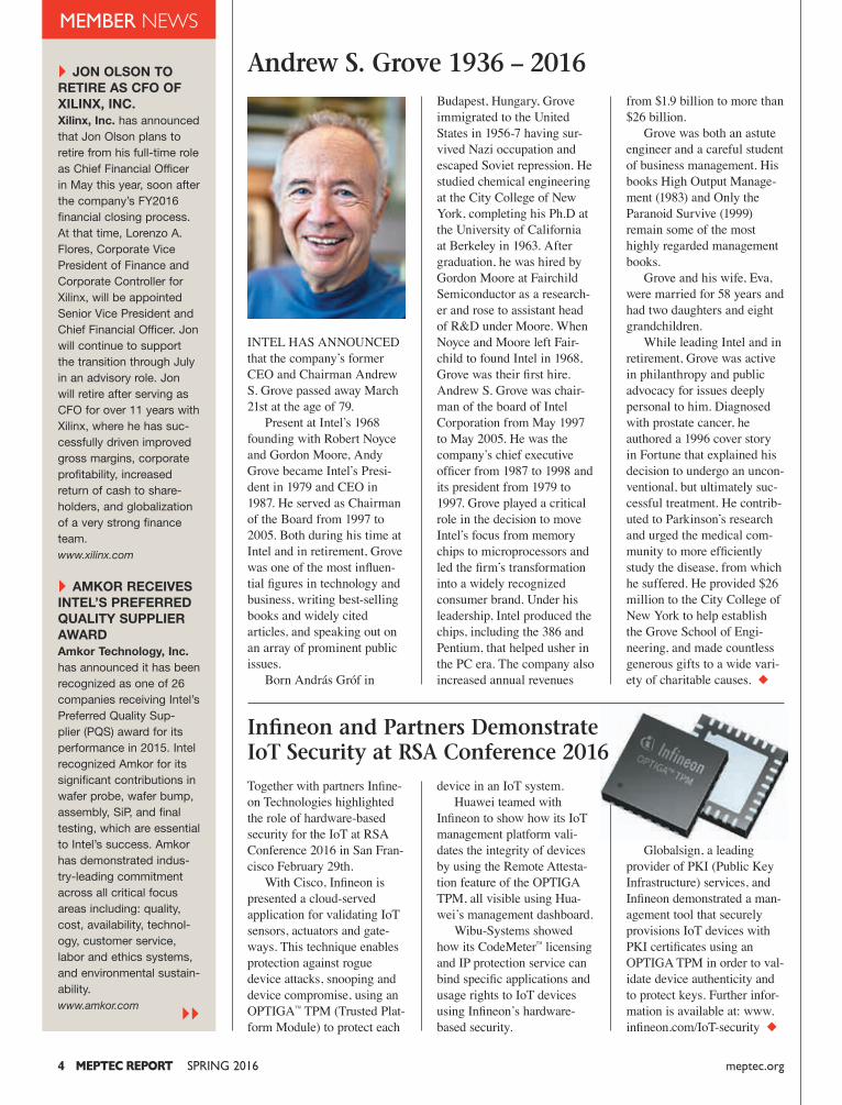
Andrew S. Grove 1936 – 2016Budapest, Hungary, Grove immigrated to the United States in 1956-7 having sur-vived Nazi occupation and escaped Soviet repression. He studied chemical engineering at the City College of New York, completing his Ph.D at the University of California at Berkeley in 1963. After graduation, he was hired by Gordon Moore at Fairchild Semiconductor as a research-er and rose to assistant head of R&D under Moore. When Noyce and Moore left Fair-child to found Intel in 1968, Grove was their first hire.Andrew S. Grove was chair-man of the board of Intel Corporation from May 1997 to May 2005. He was the company’s chief executive officer from 1987 to 1998 and its president from 1979 to 1997. Grove played a critical role in the decision to move Intel’s focus from memory chips to microprocessors and led the firm’s transformation into a widely recognized consumer brand. Under his leadership, Intel produced the chips, including the 386 and Pentium, that helped usher in the PC era. The company also increased annual revenues
INTEL HAS ANNOUNCED that the company’s former CEO and Chairman Andrew S. Grove passed away March 21st at the age of 79. Present at Intel’s 1968 founding with Robert Noyce and Gordon Moore, Andy Grove became Intel’s Presi-dent in 1979 and CEO in 1987. He served as Chairman of the Board from 1997 to 2005. Both during his time at Intel and in retirement, Grove was one of the most influen-tial figures in technology and business, writing best-selling books and widely cited articles, and speaking out on an array of prominent public issues. Born András Gróf in
from $1.9 billion to more than $26 billion. Grove was both an astute engineer and a careful student of business management. His books High Output Manage-ment (1983) and Only the Paranoid Survive (1999) remain some of the most highly regarded management books. Grove and his wife, Eva, were married for 58 years and had two daughters and eight grandchildren. While leading Intel and in retirement, Grove was active in philanthropy and public advocacy for issues deeply personal to him. Diagnosed with prostate cancer, he authored a 1996 cover story in Fortune that explained his decision to undergo an uncon-ventional, but ultimately suc-cessful treatment. He contrib-uted to Parkinson’s research and urged the medical com-munity to more efficiently study the disease, from which he suffered. He provided $26 million to the City College of New York to help establish the Grove School of Engi-neering, and made countless generous gifts to a wide vari-ety of charitable causes. ◆
Globalsign, a leading provider of PKI (Public Key Infrastructure) services, and Infineon demonstrated a man-agement tool that securely provisions IoT devices with PKI certificates using an OPTIGA TPM in order to val-idate device authenticity and to protect keys. Further infor-mation is available at: www.infineon.com/IoT-security ◆
SPRING 2016 MEPTEC REPORT 5meptec.org
1-800-776-9888
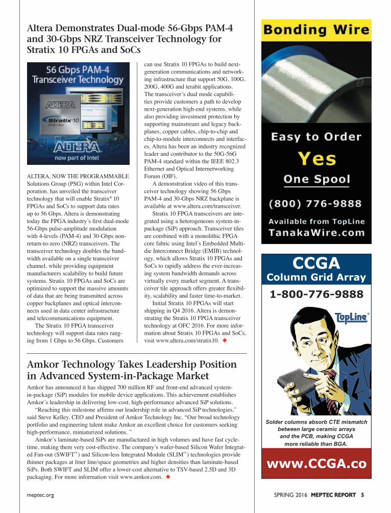
ALTERA, NOW THE PROGRAMMABLE Solutions Group (PSG) within Intel Cor-poration, has unveiled the transceiver technology that will enable Stratix® 10 FPGAs and SoCs to support data rates up to 56 Gbps. Altera is demonstrating today the FPGA industry’s first dual-mode 56-Gbps pulse-amplitude modulation with 4-levels (PAM-4) and 30-Gbps non-return-to-zero (NRZ) transceivers. The transceiver technology doubles the band-width available on a single transceiver channel, while providing equipment manufacturers scalability to build future systems. Stratix 10 FPGAs and SoCs are optimized to support the massive amounts of data that are being transmitted across copper backplanes and optical intercon-nects used in data center infrastructure and telecommunications equipment. The Stratix 10 FPGA transceiver technology will support data rates rang-ing from 1 Gbps to 56 Gbps. Customers
can use Stratix 10 FPGAs to build next-generation communications and network-ing infrastructure that support 50G, 100G, 200G, 400G and terabit applications. The transceiver’s dual mode capabili-ties provide customers a path to develop next-generation high-end systems, while also providing investment protection by supporting mainstream and legacy back-planes, copper cables, chip-to-chip and chip-to-module interconnects and interfac-es. Altera has been an industry recognized leader and contributor to the 50G-56G PAM-4 standard within the IEEE 802.3 Ethernet and Optical Internetworking Forum (OIF). A demonstration video of this trans-ceiver technology showing 56 Gbps PAM-4 and 30-Gbps NRZ backplane is available at www.altera.com/transceiver. Stratix 10 FPGA transceivers are inte-grated using a heterogeneous system-in-package (SiP) approach. Transceiver tiles are combined with a monolithic FPGA core fabric using Intel’s Embedded Multi-die Interconnect Bridge (EMIB) technol-ogy, which allows Stratix 10 FPGAs and SoCs to rapidly address the ever-increas-ing system bandwidth demands across virtually every market segment. A trans-ceiver tile approach offers greater flexibil-ity, scalability and faster time-to-market. Initial Stratix 10 FPGAs will start shipping in Q4 2016. Altera is demon-strating the Stratix 10 FPGA transceiver technology at OFC 2016. For more infor-mation about Stratix 10 FPGAs and SoCs, visit www.altera.com/stratix10. ◆
Altera Demonstrates Dual-mode 56-Gbps PAM-4 and 30-Gbps NRZ Transceiver Technology for Stratix 10 FPGAs and SoCs
Amkor has announced it has shipped 700 million RF and front-end advanced system-in-package (SiP) modules for mobile device applications. This achievement establishes Amkor’s leadership in delivering low-cost, high-performance advanced SiP solutions. “Reaching this milestone affirms our leadership role in advanced SiP technologies,” said Steve Kelley, CEO and President of Amkor Technology Inc. “Our broad technology portfolio and engineering talent make Amkor an excellent choice for customers seeking high-performance, miniaturized solutions. ” Amkor’s laminate-based SiPs are manufactured in high volumes and have fast cycle-time, making them very cost-effective. The company’s wafer-based Silicon Wafer Integrat-ed Fan-out (SWIFT™) and Silicon-less Integrated Module (SLIM™) technologies provide thinner packages at finer line/space geometries and higher densities than laminate-based SiPs. Both SWIFT and SLIM offer a lower-cost alternative to TSV-based 2.5D and 3D packaging. For more information visit www.amkor.com. ◆
Amkor Technology Takes Leadership Position in Advanced System-in-Package Market
6 MEPTEC REPORT SPRING 2016 meptec.org
An Enterprise Software Solution for Managing The Cold Chain
NOLIMITS
Any location.Any time.Any users.
M A R A T H O N P R O D U C T S
800-858-6872 www.marathon products.comDon’t ship without us®
Temperature Data LoggersOperating ranges: -80°C to 72°C. Our devices are programmed in English, Japanese, French, German, Spanish, Mandarin, and Portuguese to support globalization. Make c\temp your last Q.C. gate of product validation prior to accept- ance of critically- sensitive materials for manufacturing.
Marathon Products, Inc. headquartered in San Leandro, CA is a global supplier of investigative temperature recording devices used to validate shipments of epoxies, laminates and other critical materials used in the manufacture of integrated circuits.
An Enterprise Software Solution for Managing The Cold Chain
MEMBER NEWS
INDUSTRY’S FIRST 5G ALGORITHM INNOVATION COM-PETITION WILL HELP ACCELERATE 5G DEVELOPMENTAltera, now a part of IntelCorporation, announced the results of the 5G Algorithm InnovationCompetition, the industry’s first awards competition to focus on aligning silicon and systems companies with the research com-munity to create a pool of new and innovative ideas to help accelerate 5G, thefifth generation of mobile networks. First announced in May by Altera, now the Intel ProgrammableSolutions Group, Xidian University, and Terasic, the 5G Algorithm Innova-tion Competition was sponsored by technology leaders and gold spon-sors Huawei and Intel, and silver sponsor Spreadtrum, and attracted an impres-sive 184 teams from lead-ing universities from awide geographical area. The 184 teams consisted of 462 students from 76 universities in 31 Chinesecities. www.altera.com
ULTRATAPE ACQUIRES HIGH TECH GRAPHICS (HTG)UltraTape Industries, a division of Delphon and leading manufacturer of cleanroom tape, labels and custom adhesive material products, has announced that it has completed its acquisition of High Tech Graphics (HTG) of Sherwood, OR. HTG manufactures cus-tom graphic overlays and provides material coating services to a wide range of
INFINEON TECHNOLO-GIES AG has announced that its Digital Point-of-Load (PoL) DC-DC regulators with full PMBus capabilities are featured in the Kintex® Ultra-Scale™ development board. A key driver for the design flexibility of the board is the superior PMBus connectiv-ity of the IR3806x family. Configurations can be stored in internal memory. In addi-tion, PMBus commands allow run-time control, fault status and telemetry. The on-chip programmable SupIRBuck™
regulator provides tremendous flexibility for FPGA-based design. Thus, it easily adapts to rapidly changing design requirements. The IR3806x SupIRBuck voltage regula-tor features integrated PWM controller and MOSFETs in a single package. It delivers 90
percent more efficiency for all rails including all losses and less than sub 10 mV peak-to-peak ripple from 3 to 35 A in a tiny footprint. The regulator allows system power management on a high level and is extremely robust. Despite being compact, the IR3806x family delivers a fully integrated PoL regulator with advanced power man-agement programmability, margining, sequencing, and telemetry across multiple rails via full PMBus 1.2 compat-ibility. The board includes
all functions for an embedded processing system. This enables
designers to easily design and verify applications. The Xilinx Bit Error Test (BERT) demonstrates error losses through rigorous code testing. The IR38060 delivers precise power performance: zero bit error test results show no contribution to jitter noise across the pattern. Further information is available at: www.infineon.com/Xilinx. ◆
Infineon Enables New High-Performance FPGA Development Platform
Automated C-SAM® systems, such as the ‘dual tray - dual scanning’ DF2400, that give precisely the same image of a given component at all of a company’s locations have now been introduced by Sonoscan and are already at work in multiple plants worldwide. Called Globally Matched SonoTools™ (GMST), the new systems unleash the full potential of automation, calibration and consistency to image and qualify large num-bers of components with a minimum of human attention. At any of a company’s loca-tions, a technician selects the scan recipe for a component, pushes a button, and gets fully comparable results. For morevisit www.sonoscan.com. ◆
Globally Matched SonoTools™ Stream-line Component Inspection
SPRING 2016 MEPTEC REPORT 7meptec.org
MEMBER NEWS
industrial customers. This complementary acquisi-tion supports UltraTape’s core business and growth strategy and will allow the company to expand its offerings to include both graphic overlays and material coating. www.cleanroomtape.com
DISCO RECEIVES INTEL’S PQS AWARDDISCO Corporation has been recognized as one of 26 companies receiv-ing Intel Corporation’s Preferred Quality Sup-plier (PQS) award for their performance in 2015. DISCO has demonstrated industry-leading commit-ment across all critical focus areas on which they are measured. DISCO Corporation is recognized for their significant con-tributions providing Intel with cutting, grinding and polishing equipment and services, deemed essential to Intel’s success.www.discousa.com
CORWIL INCREASES WIRE BOND CAPABILITIESCORWIL has announced the addition of a K&S IConn Wire Bonder. This addition is one of the many new advanced pieces of equipment that CORWIL has brought to its Milpitas facility in recent months. The K&S IConn represents the state-of-the art in IC inter-Conn-ect performance for the advanced packaging requirements. “We believe that the IConn will enable us to more rapidly and accurately turn complex prototypes and volumes for our Commercial and Hi-Rel Customers,” said Willy Bowman, VP of Operations.www.corwil.com ◆
THOSE WHO WERE FORTUNATE TO have known Gene Selven recall a passion-ate, remarkable person in both business and leisure. His presence would fill a room—there was no escaping it. He was also pas-sionate in everything he did. If you are new to the industry and didn’t know Gene, there are many still around from the “good old” days that worked with him. “Gene was a terrific icon in the electronics industry,” notes Mary Ann Olsson, an industry analyst who was introduced to Gene through indus-try colleagues. “One of my first bosses always told me to call Gene for the right answers. He was always sweet and helpful to me during the early years of my electron-ics research. He was a good soul!” Born in Chicago, Illinois, Gene received his Bachelor of Science degree in Electrical Engineering from the University of Illinois in 1954, and then served in the U.S. Army from 1954-1956, stationed in Japan. Begin-ning his early career at IBM, he moved out of state to California as Manager of Prod-uct Marketing at Texas Instruments in the Semiconductor division. In 1969, he moved his residence to beautiful Portola Valley in Northern California where he began work-ing as the Director of Product Marketing at Fairchild. In 1971, he joined the Semicon-ductor Division of Raytheon as Director of Marketing.
In 1976, Gene successfully started and grew his own company and expanded into publishing—purchasing the magazine Chip Scale Review from Tessera in 1999. His daughter, Kim, continues that legacy today. An early admirer of Gene, Tom Di Stefano of Centipede Systems remembers Gene as always generous and considerate. “Gene Selven built several publications into industry standards in his lifetime,” said Di Stefano. “In his most recent endeavor, he grew Chip Scale Review to a leading position in the semiconductor industry. As an advisor to the magazine, I was always delighted by Gene’s wisdom and insight in handling the many challenges that arose.” Gene will be remembered as a true gentleman who kept his cool and resolve at all times—a true leader. Andrea Roberts of AR Marketing, says, “He was a wonderful man—and so passionate about the indus-try and communicating about it. I would always brighten up when I’d see him at a trade show. He was an institution in the industry, and although he was away from the industry for a number of years, he will be missed.” Having traveled the world several times, Gene was an international traveler both in business and his personal life. An avid fisherman, he loved to fish on Lake Tulloch, and often traveled to Alaska over the years to catch halibut and salmon. Golf was another passion. The San Francisco 49ers and Giants were his favorite teams and he was a season ticket holder of both for many years. Having grown up with the Chicago White Sox, however, it bears “special mention” that he also considered that team to be his roots. Gene is survived by his two daugh-ters, Kimberly Newman of Campbell, Cali-fornia, and Karen Williams of San Jose, California, grandson James Newman of Campbell, and his sister, Shirley Jensen of Lawton, Michigan. Services were held on March 30th. Donations can be made in Gene’s honor on the Alzheimer’s website on the (donate) tribute page under Gene Selven (www.alz.org). ◆
IN MEMORIAM A Legend, and a Life Well LivedGene Selven 1932-2016 Publisher, Chip Scale Review 1999-2008
8 MEPTEC REPORT SPRING 2016 meptec.org
SMT, COB, COF, IC ASSEMBLYSAME DAY, 1 - 5 DAYS TURN
— SMT ASSEMBLY, Lead-Free, 0201, uBGA, CSP— COB, COF, IC ASSEMBLY, Cleanroom ISO 7 (Class 10,000), Aluminum and Gold wire— NPI - PROTOTYPE, 8, 24 to 72 hours turn— Low to Medium Volume PRODUCTION, MRP, IPC-A-610 Class 2 and 3, MIL-STD-883
Your NPI Manufacturing Solution!
Phone (408) 227-8885Email: [email protected]
AmTECH is a leadingSilicon Valley providerfor SMT, COB, COF andIC Assembly.
Gold ball, aluminumand gold wedge wirebonding, AutomatedOptical Inspection(AOI) and XRAY.
www.amtechmicro.com
The difference is in the engineering
www.promex-ind.com | 408-496-0222
Promex accelerates time to market
from concept to prototype to production
Mixed-Assembly with SMT & Chip-wire•Medicaldevices(implantable,wearable,medtechequipment)
•RedundantcontinuousflowSMTassemblylines>/=01005componentplacement
•RoHScompliant&leadedsoldersystems•IPC-A-610Class3assembly
IC Packaging •Hermetic,plastic,air-cavity,COB•Multipleinterconnecttypes•Customengineeredflows(commercial,medical,military)
•Fast-trackprototypestoproductionvolumes•Class100&1000cleanrooms
ISO13485:2003●ISO9001:2008●ITARRegistered
400G to terabit chassis backplane. Xilinx teamed with TSMC to ready its PAM4 device for 16nm FinFET+ said TSMC North America vice president, Sajiv Dalal. “This transceiver break-through is another milestone in our long and rewarding collaboration with Xilinx. We share a commitment to high-perfor-mance computing, and look forward to this demonstration of Xilinx technology leadership later this month.” For additional information on the Xilinx 56G transceiver technology visit http://www.xilinx.com/products/technol-ogy/high-speed-serial/56g.html. Xilinx is the leading provider of All Programmable FPGAs, SoCs, MPSoCs, and 3D ICs. Xilinx uniquely enables applications that are both software defined and hardware optimized – powering industry advancements in Cloud Comput-ing, SDN/NFV, Video/Vision, Industrial IoT, and 5G Wireless. For more information about Xilinx visit www.xilinx.com ◆
be able to showcase our technology.” As trends such as Cloud Computing, Industrial IoT, and Software-Defined Net-works continue to accelerate and drive the need for unlimited bandwidth, technology innovations must scale to 50G, 100G, 400G ports, as well as terabit interfaces to maximize port density without increasing cost and power per bit. Next generation, standardized line rates are critical to meet-ing these ongoing bandwidth require-ments. Xilinx is leading in 56G PAM4 standardization efforts within both the Optical Internetworking Forum (OIF) and the Institute of Electrical and Electronics Engineers (IEEE). The company’s 56G PAM4 transceiver technology has been developed to break through the physical limitations of traditional data transmission at such line rates, including insertion loss and crosstalk. It supports copper and opti-cal interconnects for chip-to-chip, module, direct attach cable, or backplane applica-tions. It will enable next generation sys-tem designs for beyond terabit line cards,
XILINX, INC. HAS ANNOUNCED IT has developed a 16nm FinFET+-based programmable device running 56G trans-ceiver technology using the 4-level Pulse Amplitude Modulation (PAM4) transmis-sion scheme. Recognized by the industry as the most scalable signaling protocol for next-generation line rates, PAM4 solutions will help drive the next wave of Ethernet deployment for optical and copper inter-connects by doubling bandwidth on the existing infrastructure. Xilinx is introduc-ing and demonstrating 56G technology innovation now, ahead of general PAM4 availability, to help educate and prepare providers and ecosystem members to make this transition. “Our customers are already anticipat-ing how to accelerate their next generation applications. We recognize the need to raise awareness of 56G PAM4 technol-ogy solutions now, to help prepare them to transition their own designs,” said Ken Chang, vice president of the SerDes tech-nology group at Xilinx. “I am delighted to
Xilinx Demonstrates 56G PAM4 Transceiver TechnologyPositioned for next generation high density 400G and terabit interfaces; Enabling the next wave of Ethernet deployment
COLUMN
THE BASICS OF PERSONNEL recruitment are really quite simple. On one side, you have a candidate with some mix of skills, personality, experience, expertise, location preference and interests. On the other side, you have a company that has a need for a person with some mix of skills, personality, experience, expertise, job loca-tion and interests. Recruiting is a process that matches a particular person to a partic-ular position. This process is not unique to the employment arena. The NFL draft is an example that matches a player with certain skills to a position with a particular team ... with a lot of money involved. Arguably, one of the most basics needs of man, companionship, is a form of recruiting ... but I digress. At any point in time, there is a complex dynamic in play that involves candidates, companies, financial conditions, market segments, job functions and myriad other factors. This is often industry dependent. Even within a particular industry, however, there may be a lot of variability at any point in time. One factor that is always in play is the balance between availability of qualified and interested candidates and the number of available positions. On one end of the spectrum is a red-hot job market, typified by the high-tech sector just prior to the dot.com collapse of 2000. There were tens of thousands of jobs available and many fewer candidates. Kids straight out of college were demanding salaries in the $150,000 range and being swayed by a signing bonus of a brand new Jeep. Recruiters were covered with positions to fill, but there was a dearth of viable candidates. When we questioned the longevity of this situation, the dismissive response was we didn’t understand this was the way business was going to be in the future. An example of the other end of the spectrum is the period after the collapse when kids were moving back in with their parents (some still had their Jeeps). Recruiters had stacks of resumes on their
The Imperfect Storm
INDUSTRYINSIGHTSBy Ron Jones
desks of people who were on the beach, but there were precious few companies that were hiring. The typical situation is not one end or the other, but somewhere in between ... again very dependent on a number of fac-tors relating to industry growth, job func-tions, etc. As I mentioned in my last article, there is a very high level of merger and acquisi-tion activity in the semiconductor industry these days. In many mergers, there is a consolidation phase that includes elimina-tion of overlapping or redundant functions between the companies. This leads to lay-offs. There are always some jobs available and people that are under or unemployed to fill them. Some companies only want to hire a candidate that is currently employed. In many cases, a talented employee, par-ticularly one with a lot of experience and seniority will not want to risk leaving a rel-atively secure current job to try something unknown or risky. We approach potential candidates on a regular basis that have many years with a large company, only to be told that they are not interested in mak-ing a change or trying something new. In the last 6 months, we have seen the emergence of a new dynamic impacting some of these long term employees. They look at the level of M&A activity and are concerned for their future in a merger sce-nario. They seem to be much more likely to give serious consideration to an attrac-tive position with a new company that has a bright future. For companies that are expanding and in need to highly qualified, experienced people, there is a unique opportunity with this new-found merger driven availability of candidates. It is difficult to predict how long this situation will exist, but is an excellent opportunity for picking up very talented people. This is a unique window of opportu-nity. ◆
RON JONES is CEO of N-Able Group Inter-national; a semiconductor focused consulting and recruiting company. N-Able Group utiliz-es deep semi supply chain knowledge and a powerful cloud based software application to provide Conflict Mineral Compliance support services to companies throughout the semi-conductor supply chain including fabless, foundry, OSAT and materials suppliers. Visit www.n-ablegroup.com or email [email protected] for more information.
SPRING 2016 MEPTEC REPORT 9meptec.org
www.masterbond.com
Excellent electrical conductivity
Cryogenically serviceable
NASA low outgassing
Volume resistivity< 0.006 ohm-cm
Serviceable from 4K to 400°F
Passes ASTM E595
ONE PART EPOXY SUPREME 10HTS
Can your electrically conductive adhesive withstand the cold?
Hackensack, NJ 07601 USA+1.201.343.8983 • [email protected]
1062LK_2.25x4.60_Supreme10HTS_40yr.indd 1 1/31/16 11:55 PM
10 MEPTEC REPORT SPRING 2016 meptec.org
ANALYSIS
Emerging IoT Applications and the Importance of Packaging and Assembly E. Jan Vardaman and Trevor Yancey TechSearch International, Inc.
GROWING DEMAND FOR CONNECTED devices and systems is commonly re-ferred to as the Internet of Things (IoT), or as Cisco likes to call it, the Internet of Everything (IoE). IoT is the increased deployment of smart devices to collect data, transmit and/or process informa-tion. It is driving new requirements for packaging and assembly. This translates into an increasing number of sensors, processors or controllers, RF devices, and even memory. Which packages best meet the needs for these emerging applications? Some companies consider multi die integration a cost-effective solution for the growing connectivity requirements. Formats include a variety of packages such as leadframe, laminate substrates, fan-out wafer level packages (FO-WLP), and other alternatives. Some of these packages fall into the category of system-in-package (SiP), while others are simply miniaturized printed circuit boards (PCBs). The greatest profits may go to the software companies that provide data collection, storage, and analysis, but this does not mean that hardware is not important. The devices used for IoT and how they are designed, assembled, and packaged, are critical to the success of the products. Revenue from services related to IoT depends upon the collection of accurate data. The cost-effective assembly of the devices and the ultimate reliability of the pack-age are important.
Component Growth in IoT A number of industrial segments are expected to benefit from the use of IoT. These segments include energy production, transportation, water treat-ment plants, and factories. Capturing information using sensors is expected to be essential in all of these areas, but the required hardware and the format for the semiconductor packages used in these
applications remain to be determined. A study by PriceWaterhouse surveyed U.S. manufacturers to determine their current activities and plans for digitized manufacturing. According to the survey, 35 percent are currently collecting and using data generated by smart sensors to enhance manufacturing/operating pro-cesses, 17 percent plan to do so in the
next three years, and another 24 percent have plans but no timeline. In addition, 34 percent of manufacturers believe that it is “extremely critical” that U.S. manu-facturers adopt an IoT strategy in their operations and 60 percent believe it is slightly or moderately critical. Much of the IoT discussion is associ-ated with machine-to-machine (M2M) applications. This would include sensors, a microcontroller to capture, process, and analyze the sensor data, possibly some type of memory to store information temporarily, and a connectivity device (typically wireless) to transmit the data. An antenna is designed in the module. Miniaturization is not typically required and therefore a standard PCB with surface mount components and pack-aged die is sufficient. In cases where a plug-and-play RF solution is desired, the design may incorporate an RF solution in a SiP. Companies including TDK have designed RF modules for these appli-cations. In addition, applications that require miniaturization may need SiP.
The SiP may be in the format of a lead-frame or a laminate package, or simply a small board with components mounted on it. Smart homes include smart light-ing, safety monitors, smoke detection, temperature control, pet care, and video entertainment. Bosch estimates that by 2020, 15 percent of all households (i.e., 230 million homes) will use some form of smart home technology. According to Philips, some smart lighting applications are expected to use SiP. Augmented reality or virtual real-ity headset require motion-tracking and orientation sensors. The design of these headsets is underway and new products are expected this year. Cost-effective solutions that make the headsets less bulky will be essential to the success of these new products. The electronic content of cars is increasing and systems that provide improved safety features are an impor-tant part of the expansion. While the connected car may still be in the distant future, many safety features are already being adopted. With the expanding mar-ket for Advanced Driver Assist Systems (ADAS) driven by government regula-tions and customer demand, the use of sensors is increasing. ADAS components include many different sensors and radar modules, as well as microcontrollers. As sensors continue to be introduced for a variety of functions, the overall sensory assimilation and control will require high-speed computing and increased use of high-speed memory. Sensors from companies such as Infineon have tra-ditionally been package din leadframe packages such as SOs, SOTs, SONs, QFPs, and TSOPs. Some of the new packages are in the form of an SiP solu-tion. Both Infineon and NXP have devel-oped SiP solutions for automotive radar. (Both NXP and Freescale independently
Ultimately, package choice will be
determined by the least expensive
package that meets the performance needs.
developed fan-out wafer level package solutions. Laminate packages such as BGAs with wire bond or flip chip have also been introduced. Local interconnect networks (LIN) for automobiles may use SiP. For ex-ample, Atmel offers its ATA6613C that consists of two ICs in one package to support in-vehicle LIN networks.
Future Demand for SiP for IoT? TechSearch International defines SiP as a functional system or subsystem assembled into a standard footprint pack-age such as LGA, FBGA, QFN, or FO-WLP. It contains two or more dissimilar die, typically combined with other com-ponents such as passives, filters, MEMS, sensors, and/or antennas. The compo-nents are mounted together on a substrate to create a customized, highly integrated product for a given application. SiPs may utilize a combination of advanced packaging including bare die (wire bond or flip chip), wafer level packages, pre-packaged ICs such as CSPs, stacked
packages, stacked die, or any combina-tion of these. In some cases the package may be an embedded die solution. SiP formats include ball grid arrays (BGAs) and fine pitch BGAs (FBGAs) with laminate substrates, leadframe pack-ages such as QFPs and QFNs, stacked die packages, and other forms of 3D interconnect such as silicon interposers or 3D ICs. Where this is demand for increased performance in a small form factor, SiP will likely be adopted. Co-design, where the IC design, package, and board designers communicate will be important to the successful adoption of SiPs for IoT applications.
Critical Factors Cost-effect, high yielding assembly methods are also required. Both OSATs and EMS companies may benefit from the expansion of connectivity regardless of whether we call it IoT or IoE.
Conclusions IoT or connectivity everywhere
means there will be lots of sensors and other components, but many of the packages must be low cost to meet end product price targets. This puts pressure on the companies that will assemble the package. Ultimately, package choice will be determined by the least expensive package that meets the performance needs. ◆
SPRING 2016 MEPTEC REPORT 11meptec.org
/ Silicon Valley
JOEL CAMARDA [email protected] 415.290.6374
SemiOps Semiconductor Operations & Manufacturing Consulting
Get your manufacturing operations running efficiently and cost effectively!
Over 30 years experience in semiconductor manufacturing, operations exec and engineering management.
Trusted by Silicon Valley VCs to help make investments more profitable.
Consulting & Project Management Services:n Manufacturing & Operations – wafer fab through assembly-testn Supply chain & logistics management, supplier selection, negotiation, qualificationn Package & assembly process engineering: specific expertise in Au, Ag, Cu WB, wafer bumping, substrates, hi thermal appsn Production control, planning, business forecastingn Troubleshooting manufacturing operations, yield & productivity improvement
About TechSearch International
TechSearch International, Inc. was founded in Austin, Texas, in 1987 by E. Jan Vardaman as a technology licensing and consulting firm spe-cializing in the electronics industry. They are recognized around the world as a leading consulting com-pany in the field of advanced semi-conductor packaging technology. TechSearch International, Inc. is located at 4801 Spicewood Springs Rd., Suite 150, Austin, Texas 78759, USA, phone +1.512.372.8887.
12 MEPTEC REPORT SPRING 2016 meptec.org
SPECIAL
through front and back ends, and extremely tight control limits to yield. As the manu-facturing guy on the MEPTEC Advisory Board, this has always been my personal turn on. I look forward to semiconductors challenging the automobile for bang for the buck.
Doug Dixon, Global Marketing Director, Henkel Electronic Materials
From a geographic market perspective, it became even more obvious last year that China’s importance in the semiconductor industry is growing, as evidenced by 2015’s high profile
acquisitions: JCET acquired Singapore/Korea-based STATS ChipPAC and TSHT acquired US-based Flip Chip International. With the Chinese government providing attractive subsidies for domestic growth in semiconductors – and to compete with Tai-wan’s historical dominance – 2016 promises to be an interesting year in the region. In terms of product growth engines, the mobile segment has slowed slightly as com-pared to previous years, but still remains the fastest growing sector in the semiconductor market. Releases of multiple devices annu-ally underscore the requirement to have the right materials at the right time – a competi-tive necessity for module manufacturing and packaging houses, where time-to-market is a massive differentiator. For Henkel’s mobile R&D group, this reality drives our develop-ment timelines to ensure they align with the product delivery schedules of our custom-ers. And, of course, cost-competitiveness is always top of mind. Materials that can provide a flexibility and cost advantage – like Henkel’s conductive formulations and novel EMI shielding technologies – offer improvement in both process efficiency and profitability. Finally, what would a 2016 outlook be without a mention of wearables and IoT? With the wider adoption of wearables and
ry is also the assembly house. Many players have entered the field and already multi die formats are being developed. With the ongoing fallout of massive industry wide consolidation, the emergence of IoT and innovations enabled by technolo-gies such as 2.5/3D and FO-WLP I look forward to another exciting year in the semi-conductor packaging industry.
Joel Camarda, Principal Consultant SemiOps
We expect more advanced packaging solutions and those solutions becoming more mainstream for 2016. As our MEPTEC / SEMI Symposium of November, 2015
presented, electronic systems mobility (in your pocket, on your lap, in your body, in your vehicle, in your) requires combined technologies, smaller outlines, multi-chip solutions, and higher speed chip-to-chip communication. Some of my colleagues on the MEPTEC Advisory Board are the industry leaders in this trend, so I shall leave it to them to express those forecasts in more detail. In casual conversation, I have often expressed how I believe the modern auto-mobile epitomizes value for the dollar. If you consider the bill of materials, the expansive engineering content (mechanical and electronic), the manufacturing capital investment, it is truly amazing. I believe semiconductors are also reaching similar levels of value for the buck. At the lower end, consider you can actually purchase a low pin count, packaged, tested integrated circuit (not just a diode or transistor) for less than 2 cents. At the higher end, a multi-chip processor, including nanometer node logic, memory, possibly sensing and transmission functions, may cost over a thousand dol-lars, but consider the engineering content (both design and manufacturing), the capital investment, the multiple processing steps
Ivor Barber, Senior Director Package Technology Development, Xilinx
If 2015 was a year of consolidation, 2016 should be a year of innovation driven by new synergies or perhaps a few cases of buyer’s remorse. Consolidation should help pool resources
– many packaging innovations are becoming fab like in their capital investment profile. The silicon products of acquired or acquir-ing companies can share a broader portfolio of package technologies and patents pos-sibly enabling new products by providing innovative and cost effective package solu-tions. Controlling multiple components in a system may inspire further creative products through integration of disparate silicon products across silicon nodes and fabrica-tion sources into single package solutions be they MCM, 2.5D or 3D. The IoT continues to beckon with prom-ise of increased semiconductor content in every physical product accompanied by relentless cost pressures. A strong enabler for IOT is the explosive innovation and growth associated with MEMS devices. Readers are reminded to attend the 14th Annual MEPTEC MEMS Technology Symposium on Wednesday May 11th in San Jose. ASME has taken an interesting per-spective on IOT focusing on the hardware implementation of IoT and what it means for Component, System and Machine manu-facturers from a hardware perspective. I am honored to be the Program Chair for the inaugural ASME IoT conference which will be held in San Jose June 20 & 21. I recently attended an IEEE/CPMT Lunch Meeting led by Jan Vardaman of TechSearch International, titled FO-WLP - A Disruptive Technology: Drivers and Devel-opments. Jan explained that Fan Out Wafer Level Packaging and Wafer Level Packaging in general is a disruptive technology because it does not require a leadframe or substrate, and in the case of TSMC’s INFO the found-
Semiconductor Industry Outlook 2016MEPTEC Advisory Board
SPRING 2016 MEPTEC REPORT 13meptec.org
systems for multi-device connectivity, tra-ditional PCBs are starting to be replaced by more compact system-in-package SiP solu-tions which present interesting design and manufacturing considerations from a materi-als point of view. Mobility, wearables, IoT – all applica-tion opportunities the semiconductor indus-try embraces and, indeed, thrives on. These applications also prompt an observation, which is that the semiconductor sector has moved from an industry-driven to a con-sumer-driven market, making performance, functionality and cost the competitive tri-fecta. Those that can deliver will win!
Phil Marcoux, Vice President Package and Test SIG, Fab Owners Association
It’s 2016 – why do we still need IC packages? Recently Semi-conductor Engineer-ing posted an inter-view with Subrama-nian Iyer, professor in UCLA’s Electrical
Engineering Department and former IBM Fellow, where he raised the question of why do we use packages to house our ICs. The link for that article is http://semiengineering.com/who-needs-a-package/. For decades some of the readily accept-ed reasons were to protect the fragile chips, to enable testing, and to enable heat conduc-tion. His timing to raise this question coin-cides with the current re-emergence of mul-tichip assembly as a way to reduce the cost and risks of producing ever larger SOCs (Systems on a Chip). As Iyer notes that the NRE for a “fairly basic SoC is, at a mini-mum, $30 million to $50 million” and that by the time the chip is ready the “market has evaporated”. Around 1988/9 MCM, MultiChip Mod-ules were being heralded as the solution for many future applications. The MCM wave crested around 1991 when the issue of Known Good Die, or KGD reminded us that there was a price to be paid when chips couldn’t be fully tested before they were interconnected using expensive means, such as highly dense pcbs. Today, interest in the MCM is return-ing in the form of stacked IC s called 2.X D (2.1D - 2.5D, etc.) and 3D architectures.
When the issue of KGD is again raised the reply is often that we’re happy to accept “Good Enough Good Die”! This change in attitude is either encour-aging or shortsighted. For years many of us tried to stress that SOC die yields are often low but dismissed since many more wafers could be produced. Low yields in MCMs were never looked at with the same metric. If the current acceptance of “Good Enough” is truly “good enough” then the 2x and 3D movement may result in a new set of waves.
Rich Rice, Sr. VP Business Development, ASE Group
We are now well into 2016, and, as usual, the new year brought the typical dose of excitement, uncertainty, change, as well as the numerous and ongo-ing challenges that
our semiconductor and electronics industries face. The sputtering global economy and geopolitical concerns continue to weigh heavily upon us and while innovation is rife, visibility on solid industry growth drivers is still not clear. Our hope that lower oil prices would spur increased spending on electronics has not quite come to fruition. And, industry dynamics are compelling, to say the least. We are seeing significant con-solidation trends within the semiconductor ecosystem where players are acquiring oth-ers or are being acquired. Closer to home, the investments required for advancement of foundry technologies continue to rise each year, and it now seems that just a handful of companies will support the industry with technologies below 20nm. As we move ahead, it is still abundantly clear that the role and importance of IC packaging will continue to grow to enable the exciting array of electronics on the hori-zon. IC packaging will play a critical role and we expect wide utilization of emerging and disruptive technologies such as fan out WLP, embedded, and, high density interpos-ers, as well as continued vitality of more traditional technologies such as flip chip, wire bond, molding, and many others. These all come with their own unique sets of chal-lenges, but these are challenges that we, within the packaging community, thrive on.
John Yuanlin Xie, Ph.D., Director, PSG Packaging Technology R&DIntel Corporation
Adding to the many recent mergers and acquisitions, Altera, the company where I have worked for over 15 years, was recently acquired by Intel. Altera will operate as a new
Intel business unit called the Programmable Solutions Group (PSG). In addition to strengthening the existing FPGA business, it will revolutionize both technology and business solution roadmap for high growth data center, workstation, IoT and web search engine, etc., to deliver the next generation of highly customized, integrated products and solutions. The merger will redefine the FPGA application boundary and market cap (and market share, if you will). Initially FPGA can be integrated with selected Intel’s prod-uct lines and become part of next generation solution using multi-chip packaging solu-tions. Traditional MCP and PIP/POP with many different flavors are being considered for multiple application platforms. Innova-tive 2.5D EMIB packaging solution is also being developed for both traditional FPGA (like Stratix 10) solution as well as high per-formance computing related applications. In the future, FPGA IP can be embedded in the device as form of SoC with standard mono-lithic die packaging technologies which provides cost effective solutions for much wider range of high volume applications. Applying MCP packaging configuration with FPGA and CPU could bring significant speed improvement over using processors and FPGAs separately. Integrating the two functions in single chip, could double the performance. That combination should bring dramatic benefits for jobs like facial recognition, which might require computers to search through hundreds of millions of images to find matches. And more, integrat-ing Intel’s Atom chips with FPGAs could also help the company in new areas such as automobile electronic systems, where the ability to reprogram chips could bring new features to vehicles even after they have been sold to consumers. ◆

PROFILE
14 MEPTEC REPORT SPRING 2016 meptec.org
DESIGNING COMPLEX MEDICAL, biotech, bioscience and military products for production is a challenge. Assembly is even more demanding, as it often involves a complex series of steps to accurately locate and join components, control adhe-sive fillets, create solid interconnects, seal joints to prevent liquid leakage, etc. Extensive process engineering experi-ence with electronic and microelectronic assembly and processes is a necessity. To meet these challenges and bring products from proof of concept to full production in record time, companies turn to electron-ic manufacturing services (EMS) provid-ers such as Promex Industries Inc. Promex’s specialty is integrating conventional SMT with IC assembly for production of complex products. The company offers a mix of in-house packag-ing and engineering services, including custom QFN and substrate design, wafer
Promex Engineering, Mixed Assembly, IC Packaging Services Accelerate Time to Market from Concept to Prototype to Production
prep (thinning and dicing), die attach, wire bond, flip chip, multi-die and stacked die modules and encapsulation, along with robust, repeatable manufacturing plans. A wide array of assembly package options are also available, including COB; plastic overmolded QFN, DFN, PDIP, SOIC, BGA and flip chip; ceramic packages; multi-die substrates, and legacy plastic packages using an open-cavity process.
The Difference is in the Engineering In an industry where there is an abun-dance of contract manufacturers, Promex stands out for its deep engineering exper-tise and extensive experience. For more than 35 years, the company has been known for the high caliber of its engineer-ing staff grounded in materials science, chemistry, metallurgy, polymer science, chemical engineering, ceramic science and electrical engineering.
“We’re a how-to-build kind of com-pany that puts a premium on service – not just a factory with a lot of machines,” said Promex President and CEO Richard Otte. “We work with customers who care about quality, documentation and on-time deliv-ery because that’s what’s important to us, too.”
Promex can thin and dice 300 mm wafers.
1 2 3
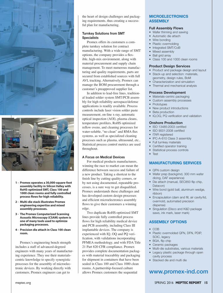
SPRING 2016 MEPTEC REPORT 15meptec.org
Promex’s engineering bench strength includes a staff of advanced-degreed engineers with many years of manufactur-ing experience. They use their materials-centric knowledge to specify synergistic processes for the assembly of microelec-tronic devices. By working directly with customers, Promex engineers can get to
the heart of design challenges and packag-ing requirements, thus creating a success-ful plan for manufacturing.
Turnkey Solutions from SMT Specialists Promex offers its customers a com-plete turnkey solution for contract manufacturing. With a wide range of SMT options, the company provides a flex-ible, high-mix environment, along with material procurement and supply chain management. To meet numerous manufac-turing and quality requirements, parts are secured from established sources with full AVL tracking. Alternatively, Promex can manage the BOM procurement through a customer’s preapproved supplier list. In addition to lead-free lines, tradition-al leaded solder system SMT/PCB assem-bly for high reliability aerospace/defense applications is readily available. Process controls include laser vision solder paste measurement, on-line x-ray, automatic optical inspection (AOI), plasma cleans, temperature profilers, RoHS optimized reflow ovens, and cleaning processes for water-soluble, “no clean” and RMA flux systems, as well as specialized cleaning processes such as plasma, ultrasound, etc.. Statistical process control metrics are used throughout.
A Focus on Medical Devices For medical products manufacturers, winning the race to market can mean the difference between success and failure of a new product. Taking a shortcut to the finish line by cutting quality corners, or by not using documented, repeatable pro-cesses, is a sure way to get disqualified. Promex understands these challenges and has developed custom design processes and efficient microelectronics assembly flows to give their customers a winning edge. Two duplicate RoHS-optimized SMT lines provide fully controlled process flows for high reliability medical device and PCB assembly, including Class III implantable devices. The company is experienced with IQ, OQ and PQ veri-fication, with validations incorporating PFMEA methodology, and with FDA Title 21 Part 820 CFR compliance. Promex provides complete documentation packag-es with material traceablity and packaging for shipment in containers that have been sealed in Class 100 and Class 1000 clean rooms. A partnership-focused culture allows Promex customers the sequential
MICROELECTRONICS ASSEMBLY
Full Assembly Flows• Wafer thinning and sawing• Automatic die attach• Wire bonding• Plastic overmolding• Integrated SMT/CoB• Mixed assembly• Ball grid array• Class 100 and 1000 clean rooms
Product Design Services• Product and package design and layout• Stack-up and selection: materials, geometry, design rules, BoM• Characterization and simulation• Thermal and mechanical analysis
Process Development• Materials-centric packaging• Custom assembly processes• Prototypes• New product introductions• Beta production• IQ,OQ, PQ verification and validation Onshore Production• ISO 13485:2003 certified• ISO 9001:2008 certified• ITAR registered• IPC-A-610 Class 3 assembly• Full turnkey materials• Certified operator training• Statistical process controls• Test
MANUFACTURING SERVICES
• QFN custom design• Wafer prep (backgrind, 300 mm wafer dicing, DAF experience)• Die attach (manual, SEC850 flip chip, Datacon)• Wire bond (gold ball, aluminum wedge, ribbon)• Encapsulation (dam and fill, air cavity/lid, overmold, automated precision dispense)• Singulation (Disco and K&D package saws, ink mark, laser mark)
ASSEMBLY OPTIONS
• COB• Plastic overmolded QFN, DFN, PDIP, SOIC, legacy• BGA, flip chip• Ceramic packages• Multi-die substrates, various materials• Legacy plastic package through open cavity process• Stacked die and multi die
1 - Promex operates a 30,000-square-foot assembly facility in Silicon Valley with RoHS-optimized SMT, Class 100 and 1000 clean rooms and fully controlled process flows for high reliability.
2 - Multi-die stack illustrates Promex engineering expertise and mixed assembly processes.
3 - The Promex Computerized Scanning Acoustic Microscopy (CSAM) system is one of many tools used to optimize packaging processes.
4 - Precision die attach in Class 100 clean room.
www.promex-ind.com
4

PROFILE
16 MEPTEC REPORT SPRING 2016 meptec.org
steps of prototyping through volume pro-duction for:
• Implantable devices utilizing long-life electronics that can be integrated into small, easily implantable modules
• Image sensors manufactured utilizing processes that eliminate particle con- tamination. Promex can integrate sensors of different types into small assemblies, including optical assem- bly and precision placement of com- plex stacked assemblies
• Diagnostic equipment requiring highly trained personnel with experience mounting small parts, including 0201 and 01005 SMT parts, micro BGAs and chip scale packages
• Disposable diagnostic devices that require a combination of electronics and sensors in a small, low-cost device
Quik-Pak Delivers Packaging Time-to-Market Advantage Promex recently acquired Quik-Pak, a San Diego-based company providing IC packaging solutions for complex semi-conductors. The company specializes in reducing time to market through all phas-es of packaging, from prototype design validation to full production and offers fast-turn assembly services for ceramic, laminate, COF and COB. Custom transfer molded packaging and wafer preparation services, including dicing, backgrinding and pick-and-place, are also available. The company’s 15,000-square-foot facility features fully automated equip-ment. A Datacon 2200 EVO high-accu-racy multi-chip die bonder provides the ultimate flexibility for die attach, as well as, for flip chip applications. It is equipped with asynchronous dispense heads, an automatic tool changer, inverter, fluxing stations and application-specific tooling. K&S high-performance wire bonders can accommodate gold wire diameters down to 15 microns. Quik-Pak specializes in air cavity plastic QFN packages. Its flagship product is a new Open-molded Plastic Package
ment of sizes from 3x3 mm to 12x12 mm, with a variety of pitch options and lead counts. Quantities from prototype to production volumes are available. Custom configurations can also be designed and manufactured. “We’ve seen a significant increase in the assembly of flip chip devices at both package and board level assembly,” said Quik-Pak General Manager Steve Swend-rowski. “Quik-Pak continues to meet our customers’ expectations regardless of the assembly technology”. For more information about Promex Industries, contact Director of Sales and Marketing Rosie Medina at 408-496-0222 or visit www.promex-ind.com. For more information about Quik-Pak, contact Director of Sales and Marketing Casey Krawiec at 858-674-4676 or visit www.icproto.com. ◆
(OmPP) providing superior bondability and electrical performance. Made from an RoHS- and REACH-compliant green molding compound, this Au/Ni-plated QFN package is available in an assort-
Quik-Pak specializes in multi-chip and stacked-die assemblies in air cavity QFN (OmPP) packages.
Thought Leadership for Advanced Manufacturing
Promex is an active supporter of MEPTEC and a frequent pre-senter at its events. For example, at a recent MEPTEC West Coast luncheon, Promex President and CEO Dick Otte presented “The QFN Platform as a Chip Packaging Foundation.” Otte discussed how the QFN-type packaging concept, originally a single die JEDEC stan-dard packaging method, is being expanded to include multi die, stacked die, system-in-package and complex multi-chip modules utiliz-ing custom lead frames or a variety of organic substrates. Today, the QFN assembly and packaging plat-form is considered a gateway for advanced packaging that improves time to market. Promex’s thought leadership extends beyond the microelectron-ics assembly and packaging indus-try. Recently the National Institute for Standards and Technology (NIST) selected a team from the MIT Microphotonics Center and the International Electronics Manufac-turing Initiative (iNEMI) to develop a roadmap for photonics. That team was named the Photonics Systems
Manufacturing Consortium (PSMC). Promex President and CEO Dick Otte was selected to chair the PSMC’s Assembly and Test Work-ing Group. Earlier this year he pre-sented a webinar addressing the integrated photonics requirements required to minimize cost while achieving functionality and meet tight mechanical tolerances for opti-cal devices. Last year, US Vice President Joe Biden announced the formation of the American Institute for Manufac-turing Integrated Photonics (AIM IP), one of several institutes under a new national initiative called the National Network for Manufacturing Innovation (NNMI). PSMC has now joined with AIM IP and will continue working with the Institute to develop roadmaps for integrated photonics. Promex is proud to be an integral part of this initiative to strengthen America’s leadership in advanced manufacturing.
Promex President and CEO Richard Otte
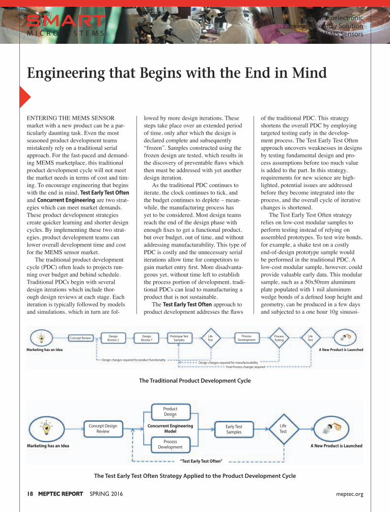
ENTERING THE MEMS SENSOR market with a new product can be a par-ticularly daunting task. Even the most seasoned product development teams mistakenly rely on a traditional serial approach. For the fast-paced and demand-ing MEMS marketplace, this traditional product development cycle will not meet the market needs in terms of cost and tim-ing. To encourage engineering that begins with the end in mind, Test Early Test Often and Concurrent Engineering are two strat-egies which can meet market demands. These product development strategies create quicker learning and shorter design cycles. By implementing these two strat-egies, product development teams can lower overall development time and cost for the MEMS sensor market. The traditional product development cycle (PDC) often leads to projects run-ning over budget and behind schedule. Traditional PDCs begin with several design iterations which include thor-ough design reviews at each stage. Each iteration is typically followed by models and simulations, which in turn are fol-
of the traditional PDC. This strategy shortens the overall PDC by employing targeted testing early in the develop-ment process. The Test Early Test Often approach uncovers weaknesses in designs by testing fundamental design and pro-cess assumptions before too much value is added to the part. In this strategy, requirements for new science are high-lighted, potential issues are addressed before they become integrated into the process, and the overall cycle of iterative changes is shortened. The Test Early Test Often strategy relies on low-cost modular samples to perform testing instead of relying on assembled prototypes. To test wire bonds, for example, a shake test on a costly end-of-design prototype sample would be performed in the traditional PDC. A low-cost modular sample, however, could provide valuable early data. This modular sample, such as a 50x50mm aluminum plate populated with 1 mil aluminum wedge bonds of a defined loop height and geometry, can be produced in a few days and subjected to a one hour 10g sinusoi-
lowed by more design iterations. These steps take place over an extended period of time, only after which the design is declared complete and subsequently “frozen”. Samples constructed using the frozen design are tested, which results in the discovery of preventable flaws which then must be addressed with yet another design iteration. As the traditional PDC continues to iterate, the clock continues to tick, and the budget continues to deplete – mean-while, the manufacturing process has yet to be considered. Most design teams reach the end of the design phase with enough fixes to get a functional product, but over budget, out of time, and without addressing manufacturability. This type of PDC is costly and the unnecessary serial iterations allow time for competitors to gain market entry first. More disadvanta-geous yet, without time left to establish the process portion of development, tradi-tional PDCs can lead to manufacturing a product that is not sustainable. The Test Early Test Often approach to product development addresses the flaws
Engineering that Begins with the End in Mind
18 MEPTEC REPORT SPRING 2016 meptec.org
Your Microelectronic Package Assembly Solution
for MEMS Sensors
The Test Early Test Often Strategy Applied to the Product Development Cycle
Marketing has an Idea
Concurrent EngineeringModel
A New Product is Launched
“Test Early Test Often”
ProductDesign
Concept DesignReview
LifeTest
Early Test Samples
ProcessDevelopment
The Traditional Product Development Cycle
Marketing has an Idea A New Product is Launched
Concept Review Design Review 2
Design changes required for product functionality
Design Review ?
Prototype TestSamples
LifeTest
ProcessDevelopment
LifeTest
Process Testing
Design changes required for manufacturabilityFinal Process changes required
Your Microelectronic Package Assembly Solution for MEMS Sensors141 Innovation Drive, Elyria, Ohio 44035 • [email protected]
www.smartmicrosystems.com
Test Early, Test Often.Significantly Lower Overall Development Time and Cost
SMART Microsystems creates turn-key solutions for microelectronic package assembly challenges to move your MEMS sensor technology from development to production. With an engineering team experienced in manufacturing and state-of-the-art facilities, SMART Microsystems accelerates the transition of your new MEMS sensor product to the market.
Call us today at 440-366-4203 or visit our website at www.smartmicrosystems.com for more information about SMART Microsystems capabilities and services.
For the fast-paced and demanding MEMS marketplace, the traditional product development cycle (PDC) will not meet the market needs in terms of cost and timing. The Test Early Test Often approach addresses the flaws of the traditional product development cycle. This strategy shortens the overall PDC by employing targeted test-ing early in the development process. The Test Early Test Often approach uncovers weaknesses in designs by testing fundamental design and process assumptions before too much value is added to the part.
The Test Early Test Often strategy relies on low-cost modular samples to perform testing instead of relying on assembled prototypes. Results can be analyzed in multiple ways, including optical and acoustic microscopy, X-Ray, and SEM. And most tests can be completed in less than a week, with the learning incorporated into the early stages of the design and process engineering. The Test Early Test Often approach also takes advantage of rapid prototyping to implement targeted tests to create quicker learning and shorter design cycles, allowing product development teams to lower overall development time and cost for the MEMS sensor market.
Hitachi Series 4500 Sonoscan Acoustic MicroscopeNordson X-ray Nordson Dage Bond Tester
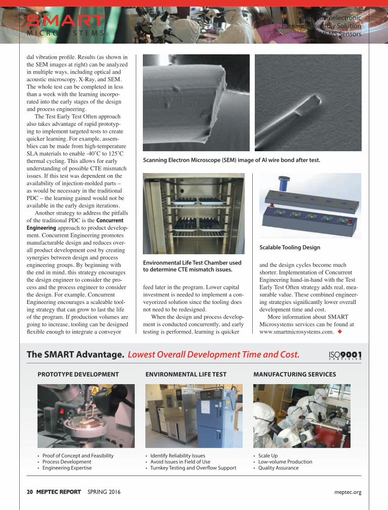
The SMART Advantage. Lowest Overall Development Time and Cost.
PROTOTYPE DEVELOPMENT ENVIRONMENTAL LIFE TEST MANUFACTURING SERVICES
• Proof of Concept and Feasibility• Process Development• Engineering Expertise
• Identify Reliability Issues• Avoid Issues in Field of Use• Turnkey Testing and Overflow Support
• Scale Up• Low-volume Production• Quality Assurance
20 MEPTEC REPORT SPRING 2016 meptec.org
Your Microelectronic Package Assembly Solution
for MEMS Sensors
and the design cycles become much shorter. Implementation of Concurrent Engineering hand-in-hand with the Test Early Test Often strategy adds real, mea-surable value. These combined engineer-ing strategies significantly lower overall development time and cost. More information about SMART Microsystems services can be found at www.smartmicrosystems.com. ◆
feed later in the program. Lower capital investment is needed to implement a con-veyorized solution since the tooling does not need to be redesigned. When the design and process develop-ment is conducted concurrently, and early testing is performed, learning is quicker
dal vibration profile. Results (as shown in the SEM images at right) can be analyzed in multiple ways, including optical and acoustic microscopy, X-Ray, and SEM. The whole test can be completed in less than a week with the learning incorpo-rated into the early stages of the design and process engineering. The Test Early Test Often approach also takes advantage of rapid prototyp-ing to implement targeted tests to create quicker learning. For example, assem-blies can be made from high-temperature SLA materials to enable -40˚C to 125˚C thermal cycling. This allows for early understanding of possible CTE mismatch issues. If this test was dependent on the availability of injection-molded parts – as would be necessary in the traditional PDC – the learning gained would not be available in the early design iterations. Another strategy to address the pitfalls of the traditional PDC is the Concurrent Engineering approach to product develop-ment. Concurrent Engineering promotes manufacturable design and reduces over-all product development cost by creating synergies between design and process engineering groups. By beginning with the end in mind, this strategy encourages the design engineer to consider the pro-cess and the process engineer to consider the design. For example, Concurrent Engineering encourages a scaleable tool-ing strategy that can grow to last the life of the program. If production volumes are going to increase, tooling can be designed flexible enough to integrate a conveyor
Scanning Electron Microscope (SEM) image of Al wire bond after test.
Environmental Life Test Chamber used to determine CTE mismatch issues.
Scalable Tooling Design
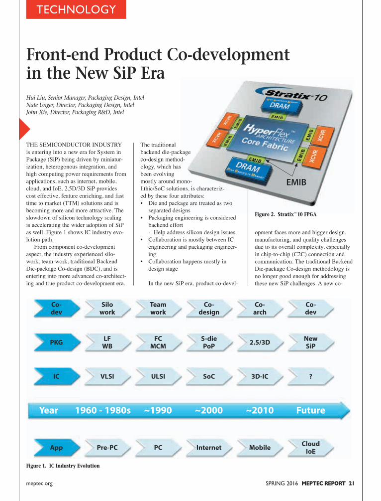
EMIB
opment faces more and bigger design, manufacturing, and quality challenges due to its overall complexity, especially in chip-to-chip (C2C) connection and communication. The traditional Backend Die-package Co-design methodology is no longer good enough for addressing these new SiP challenges. A new co-
The traditional backend die-package co-design method-ology, which has been evolving mostly around mono-lithic/SoC solutions, is characteriz-ed by these four attributes:• Die and package are treated as two separated designs• Packaging engineering is considered backend effort - Help address silicon design issues• Collaboration is mostly between IC engineering and packaging engineer- ing• Collaboration happens mostly in design stage In the new SiP era, product co-devel-
THE SEMICONDUCTOR INDUSTRY is entering into a new era for System in Package (SiP) being driven by miniatur-ization, heterogonous integration, and high computing power requirements from applications, such as internet, mobile, cloud, and IoE. 2.5D/3D SiP provides cost effective, feature enriching, and fast time to market (TTM) solutions and is becoming more and more attractive. The slowdown of silicon technology scaling is accelerating the wider adoption of SiP as well. Figure 1 shows IC industry evo-lution path. From component co-development aspect, the industry experienced silo-work, team-work, traditional Backend Die-package Co-design (BDC), and is entering into more advanced co-architect-ing and true product co-development era.
Front-end Product Co-development in the New SiP Era
TECHNOLOGY
Figure 2. Stratix™ 10 FPGA
Hui Liu, Senior Manager, Packaging Design, IntelNate Unger, Director, Packaging Design, IntelJohn Xie, Director, Packaging R&D, Intel
Figure 1. IC Industry Evolution
Co-dev
Silowork
Teamwork
Co-design
Co-arch
Co-dev
App Pre-PC PC Internet Mobile CloudIoE
IC VLSI ULSI SoC 3D-IC ?
PKG LFWB
FCMCM
S-diePoP 2.5/3D New
SiP
Year 1960 - 1980s ~1990 ~2000 ~2010 Future
SPRING 2016 MEPTEC REPORT 21meptec.org
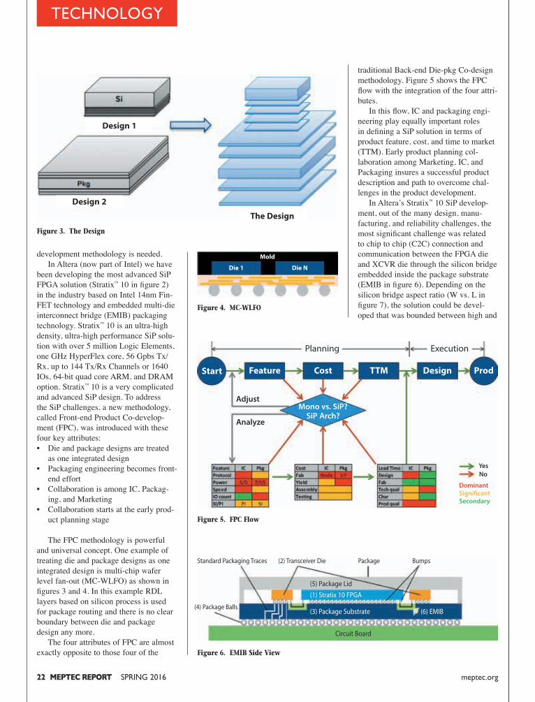
traditional Back-end Die-pkg Co-design methodology. Figure 5 shows the FPC flow with the integration of the four attri-butes. In this flow, IC and packaging engi-neering play equally important roles in defining a SiP solution in terms of product feature, cost, and time to market (TTM). Early product planning col-laboration among Marketing, IC, and Packaging insures a successful product description and path to overcome chal-lenges in the product development. In Altera’s Stratix™ 10 SiP develop-ment, out of the many design, manu-facturing, and reliability challenges, the most significant challenge was related to chip to chip (C2C) connection and communication between the FPGA die and XCVR die through the silicon bridge embedded inside the package substrate (EMIB in figure 6). Depending on the silicon bridge aspect ratio (W vs. L in figure 7), the solution could be devel-oped that was bounded between high and
development methodology is needed. In Altera (now part of Intel) we have been developing the most advanced SiP FPGA solution (Stratix™ 10 in figure 2) in the industry based on Intel 14nm Fin-FET technology and embedded multi-die interconnect bridge (EMIB) packaging technology. Stratix™ 10 is an ultra-high density, ultra-high performance SiP solu-tion with over 5 million Logic Elements, one GHz HyperFlex core, 56 Gpbs Tx/Rx, up to 144 Tx/Rx Channels or 1640 IOs, 64-bit quad core ARM, and DRAM option. Stratix™ 10 is a very complicated and advanced SiP design. To address the SiP challenges, a new methodology, called Front-end Product Co-develop-ment (FPC), was introduced with these four key attributes:• Die and package designs are treated as one integrated design• Packaging engineering becomes front- end effort• Collaboration is among IC, Packag- ing, and Marketing• Collaboration starts at the early prod- uct planning stage
The FPC methodology is powerful and universal concept. One example of treating die and package designs as one integrated design is multi-chip wafer level fan-out (MC-WLFO) as shown in figures 3 and 4. In this example RDL layers based on silicon process is used for package routing and there is no clear boundary between die and package design any more. The four attributes of FPC are almost exactly opposite to those four of the
Figure 3. The Design
Design 1
Design 2
The Design
Figure 4. MC-WLFO
Die 1 Die N
Mold
Figure 5. FPC Flow
Yes No
DominantSignificantSecondary
Planning Execution
Start Feature Cost TTM Design Prod
Analyze
AdjustMono vs. SiP?
SiP Arch?
Figure 6. EMIB Side View
Standard Packaging Traces (2) Transceiver Die Package Bumps
(4) Package Balls
(1) Stratix 10 FPGA
Circuit Board
(3) Package Substrate (6) EMIB
(5) Package Lid
22 MEPTEC REPORT SPRING 2016 meptec.org
TECHNOLOGY
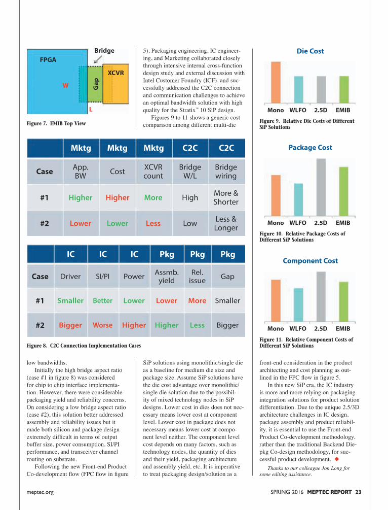
SPRING 2016 MEPTEC REPORT 23meptec.org
front-end consideration in the product architecting and cost planning as out-lined in the FPC flow in figure 5. In this new SiP era, the IC industry is more and more relying on packaging integration solutions for product solution differentiation. Due to the unique 2.5/3D architecture challenges in IC design, package assembly and product reliabil-ity, it is essential to use the Front-end Product Co-development methodology, rather than the traditional Backend Die-pkg Co-design methodology, for suc-cessful product development. ◆ Thanks to our colleague Jon Long for some editing assistance.
5), Packaging engineering, IC engineer-ing, and Marketing collaborated closely through intensive internal cross-function design study and external discussion with Intel Customer Foundry (ICF), and suc-cessfully addressed the C2C connection and communication challenges to achieve an optimal bandwidth solution with high quality for the Stratix™ 10 SiP design. Figures 9 to 11 shows a generic cost comparison among different multi-die
low bandwidths. Initially the high bridge aspect ratio (case #1 in figure 8) was considered for chip to chip interface implementa-tion. However, there were considerable packaging yield and reliability concerns. On considering a low bridge aspect ratio (case #2), this solution better addressed assembly and reliability issues but it made both silicon and package design extremely difficult in terms of output buffer size, power consumption, SI/PI performance, and transceiver channel routing on substrate. Following the new Front-end Product Co-development flow (FPC flow in figure
SiP solutions using monolithic/single die as a baseline for medium die size and package size. Assume SiP solutions have the die cost advantage over monolithic/single die solution due to the possibil-ity of mixed technology nodes in SiP designs. Lower cost in dies does not nec-essary means lower cost at component level. Lower cost in package does not necessary means lower cost at compo-nent level neither. The component level cost depends on many factors, such as technology nodes, the quantity of dies and their yield, packaging architecture and assembly yield, etc. It is imperative to treat packaging design/solution as a
Figure 7. EMIB Top View
FPGABridge
XCVR
GapW
L
Figure 11. Relative Component Costs of Different SiP Solutions
Mono WLFO 2.5D EMIB
Component Cost
Figure 10. Relative Package Costs of Different SiP Solutions
Mono WLFO 2.5D EMIB
Package Cost
Figure 9. Relative Die Costs of Different SiP Solutions
Mono WLFO 2.5D EMIB
Die Cost
MktgMktgMktg C2C C2C
Case App.BW Cost XCVR
countBridge
W/LBridge wiring
#1 Higher Higher More High More & Shorter
#2 Lower Lower Less Low Less & Longer
Figure 8. C2C Connection Implementation Cases
Case Driver SI/PI Power Assmb.yield
Rel.issue Gap
#1 Smaller Better Lower Lower More Smaller
#2 Bigger Worse Higher Higher Less Bigger
IC IC IC Pkg Pkg Pkg
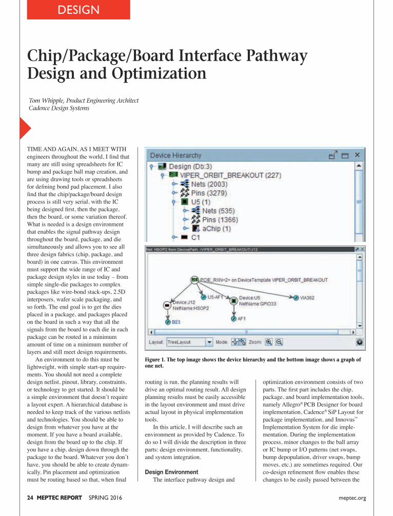
24 MEPTEC REPORT SPRING 2016 meptec.org
DESIGN
Chip/Package/Board Interface Pathway Design and Optimization
optimization environment consists of two parts. The first part includes the chip, package, and board implementation tools, namely Allegro® PCB Designer for board implementation, Cadence® SiP Layout for package implementation, and Innovus™
Implementation System for die imple-mentation. During the implementation process, minor changes to the ball array or IC bump or I/O patterns (net swaps, bump depopulation, driver swaps, bump moves, etc.) are sometimes required. Our co-design refinement flow enables these changes to be easily passed between the
routing is run, the planning results will drive an optimal routing result. All design planning results must be easily accessible in the layout environment and must drive actual layout in physical implementation tools. In this article, I will describe such an environment as provided by Cadence. To do so I will divide the description in three parts: design environment, functionality, and system integration.
Design Environment The interface pathway design and
TIME AND AGAIN, AS I MEET WITH engineers throughout the world, I find that many are still using spreadsheets for IC bump and package ball map creation, and are using drawing tools or spreadsheets for defining bond pad placement. I also find that the chip/package/board design process is still very serial, with the IC being designed first, then the package, then the board, or some variation thereof. What is needed is a design environment that enables the signal pathway design throughout the board, package, and die simultaneously and allows you to see all three design fabrics (chip, package, and board) in one canvas. This environment must support the wide range of IC and package design styles in use today – from simple single-die packages to complex packages like wire-bond stack-ups, 2.5D interposers, wafer scale packaging, and so forth. The end goal is to get the dies placed in a package, and packages placed on the board in such a way that all the signals from the board to each die in each package can be routed in a minimum amount of time on a minimum number of layers and still meet design requirements. An environment to do this must be lightweight, with simple start-up require-ments. You should not need a complete design netlist, pinout, library, constraints, or technology to get started. It should be a simple environment that doesn’t require a layout expert. A hierarchical database is needed to keep track of the various netlists and technologies. You should be able to design from whatever you have at the moment. If you have a board available, design from the board up to the chip. If you have a chip, design down through the package to the board. Whatever you don’t have, you should be able to create dynam-ically. Pin placement and optimization must be routing based so that, when final
Tom Whipple, Product Engineering Architect Cadence Design Systems
Figure 1. The top image shows the device hierarchy and the bottom image shows a graph of one net.
SPRING 2016 MEPTEC REPORT 25meptec.org
wide variety of ball and bump pin pat-terns. You may generate regular ring and array, staggered and in-line, and irregular patterns. Rule-based patterns may be generated on a block-by-block basis, and regular patterns may be saved and repli-cated throughout the part. In the early stages of pin design, it is important to be able to define the signal, power, and ground patterns for pins of a device. But all too often these definitions are created in a spreadsheet and then man-ually transferred to the physical design. Two solutions to automating this process are provided in the OrbitIO sys-tem planner. First is to create the signal, power, and ground patterns on a pin array (bump or ball), then assign signals, power, and ground to that array. As shown in Figure 3, different patterns can be used in different parts of the design depending on requirements. The second approach is to define sig-nal, power, and ground ratios in the inter-face floorplans (see next section). As the floorplans are mapped to the pins of the device, power and ground pins are also reserved in the correct signal-to-power-to-ground ratios.
Bundling with Interfaces Typical layout tools enable the layout of signals on a signal-by-signal or pin-by-pin basis. Automatic and manual routing tools also work on a signal-by-signal
I/O Pad Creation and Optimization The OrbitIO system planner greatly simplifies I/O pad placement and align-ment. It is especially useful in a wire bond die stack where you need to align I/O pads between dies in a die stack or between side-by-side dies (see Figure 2). Pin Pattern Generation Every designer, device, and project has different pin pattern and pin assignment requirements. The OrbitIO system planner provides you with the ability to create a
package and IC design tools. The users of these tools are the respective board, pack-age, and IC designers, and changes to the interfaces are shared by exchange of the relevant files. The second is the multi-fabric design and optimization flow, which is enabled by OrbitIO™ system planner, a hierarchical “start-from-whatever-you-have” design environment. When I say hierarchical, I mean you can import an existing PCB file, place a package in it, and place several dies in the package. The net name space is preserved throughout the design hierarchy (see Figure 1). In one design canvas, you can view the PCB, package, and die, and assign and optimize pinouts in the context of the whole system. The technology, dimensions, and layer stack-up informa-tion for each device is preserved, and the net name space of each device is pre-served. You may even import dies from different technology nodes. “Start-from-whatever-you-have” means exactly what it says. You do not have to have a full layer stack-up or full constraint deck setup. You do not need a full netlist or full device library. You don’t have to have anything to get started. Any-thing you don’t have, you create on the fly. Anything you do have, you use. The user of the OrbitIO interconnect designer may be a package layout engineer, but could also be an IC designer, product engineer, or a product architect. It doesn’t take a package or board layout expert to use the OrbitIO system planner – it is intended to be lightweight, easy to get started, and easy to use.
Functionality Key functionality that enables pathway design and optimization consists of topol-ogy exploration, I/O pad creation and optimization, pin pattern generation, bun-dling with interfaces, breakout feasibility routing, and variants.
Topology Exploration Topology exploration is the defining of where each function will be designed in the system – on the chip, in the package, in the board, on an interposer, etc. The OrbitIO system planner’s unique hierar-chical architecture makes it easy to move components and functions between the die, the package, and the board so you can quickly explore different design solutions.
Figure 2. Package with three wire bond dies. On the left side, the yellow die is on top of the grey die. Another grey die is on the right. Red lines show connections between I/O drivers aligned between dies in the two stacks and the BGA.
Figure 3: BGA ball array with signal, power, and ground planning completed and with some net assignments completed.
26 MEPTEC REPORT SPRING 2016 meptec.org
DESIGN
variant designs. So often, a single die will be placed into several different packages. Or a single package will be placed in several different PCB variations. You can place each variation in the OrbitIO system planner and explore the solution space. For example, you can place multiple pack-ages, then instantiate a die in each pack-age. This process is all done in a single canvas so you can see all variants at once. As changes are made to one instance of the die, it is reflected in all instances of the die (see Figure 6) so you can see how the changes affect each variant, making it easy to explore options, make tradeoffs,
basis. However, a look at a typical ball map in a spreadsheet shows the pins are often grouped and colored by function, or in other words, by interface. The OrbitIO system planner enables you to easily iden-tify the interfaces in your design and then map out the pathway for the signals of the interface between board component pins, package pins, and die pins. The bundle preserves the order of signals at the bundle entry. The bundle is then drawn to model the approximate routing pathway of the signals to another component, and the signals are automatically assigned to pins on the destination component in the same order they were in at the other end of the bundle. Bundles are created either manu-ally or automatically. Because bundling enables you to plan your BGA and die pin assignments so they align nicely with pins on the board while taking into account the routing pathways in both the board and the package (see Figure 4), it provides a great first-order pin assignment solution. When doing bundle-based net assign-ment, differential pairs are recognized and are placed on adjacent pins. Cross-bars are displayed to show the diff pair relation-ship, as shown in Figure 5. Breakout Feasibility Routing The next level of pathway optimiza-tion comes through the use of breakout routing. If breakout routing already exists for a component, it will drive the signal order in a bundle. If breakout routing does not exist, the OrbitIO system planner may be used to generate feasibility breakout route patterns. These patterns show if your pin assignment will be able to be broken out on the layers you have selected. You optimize the pathway by either swapping pins, swapping interfaces, or changing the breakout sequence. By planning the signal pathway in the context of the whole system, you are given many degrees of freedom in the optimization process. You may optimize at the board components, the package pin assignments, package breakout (on the PCB substrate), package break-in (on the package substrate), die breakout, I/O driver placement, and die pin assignments.
Variants Because of the OrbitIO system plan-ner’s hierarchical architecture, it is easy to use all that has been discussed above in
Figure 5. Differential pair net assignment with bundle. Diff pairs are color-coded and a cross-bar visually links both pins of the pair.
Figure 4. The top image above shows two bundles: one from a memory component to the BGA, and another from a connector to the BGA. The bottom left image shows the bundle coming off breakouts from the memory component. The bundle signal sequence is defined from these breakouts. The bottom right image shows both bundles connected to the BGA breakouts. The signal sequence at the BGA is defined by the memory and component break-out order.
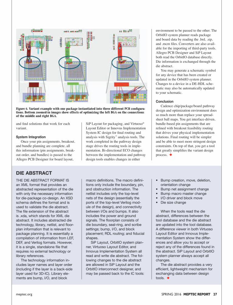
SPRING 2016 MEPTEC REPORT 27meptec.org
environment to be passed to the other. The OrbitIO system planner reads package and board data by reading the .brd, .sip, and .mcm files. Converters are also avail-able for the importing of third-party tools. Allegro PCB Designer and SiP Layout both read the OrbitIO database directly. Die information is exchanged through the die abstract. You may generate a schematic symbol for any device that has been created or updated in the OrbitIO system planner. Changes to a device in a DE-HDL sche-matic may also be automatically updated to your schematic.
Conclusion Cadence chip/package/board pathway design and optimization environment does so much more than replace your spread-sheet ball maps. You get interface-driven, bundle-based pin assignments that are refined with breakout feasibility routing that drives your physical implementation solutions. Final routing will be simpler and be able to meet more stringent design constraints. On top of that, you get a tool that greatly simplifies the variant design process. ◆
SiP Layout for packaging, and Virtuoso®
Layout Editor or Innovus Implementation System IC design for final routing and analysis with Sigrity™ analysis tools. The work completed in the pathway design stage drives the routing tools in imple-mentation. Bi-directional ECO changes between the implementation and pathway design tools enables changes in either
and find solutions that work for each variant. System Integration Once your pin assignments, breakout, and bundle planning are complete, all this information (pin assignments, break-out order, and bundles) is passed to the Allegro PCB Designer for board layout,
Figure 6. Variant example with one package instantiated into three different PCB configura-tions. Bottom zoomed-in images show effects of optimizing the left BGA on the connections of the middle and right BGA.
DIE ABSTRACTTHE DIE ABSTRACT FORMAT IS an XML format that provides an abstracted representation of the die with only the necessary information for die-package co-design. An XSD schema defines the format and is used to validate the die abstract. The file extension of the abstract is .xda, which stands for XML die abstract. It includes abstracted die technology, library, netlist, and floor-plan information that is relevant to package planning. It is essentially a compilation of information from LEF, DEF, and Verilog formats. However, it is a single, standalone file that requires no external technology or library references. The technology information in-cludes layer names and layer order (including if the layer is a back-side layer used for 3D-IC). Library ele-ments are bump, I/O, and block
macro definitions. The macro defini-tions only include the boundary, pin, and obstruction information. The netlist includes only the top-level nets of the design (essentially the ports of the top-level Verilog mod-ule of the design), and connectivity between I/Os and bumps. It also includes the power and ground signals. The floorplan consists of die boundary, seal-ring, and scribe settings; bump, I/O, and block placement; RDL routing; and fiducial shapes. SiP Layout, OrbitIO system plan-ner, Virtuoso Layout Editor, and Innovus Implementation System all read and write die abstract. The fol-lowing changes to the die abstract are allowed in SiP Layout and the OrbitIO interconnect designer, and may be passed back to the IC tools:
• Bump creation, move, deletion, orientation change• Bump net assignment change• Bump macro master change• I/O driver and block move• Die size change
When the tools read the die abstract, differences between the tool database and the die abstract are updated into the tool database. A difference viewer in both Virtuoso Layout Editor and Innovus Imple-mentation System show the differ-ences and allow you to accept or reject any of the differences found in the abstract. SiP Layout and OrbitIO system planner always accept all changes. The die abstract provides a very efficient, lightweight mechanism for exchanging data between design tools. ◆
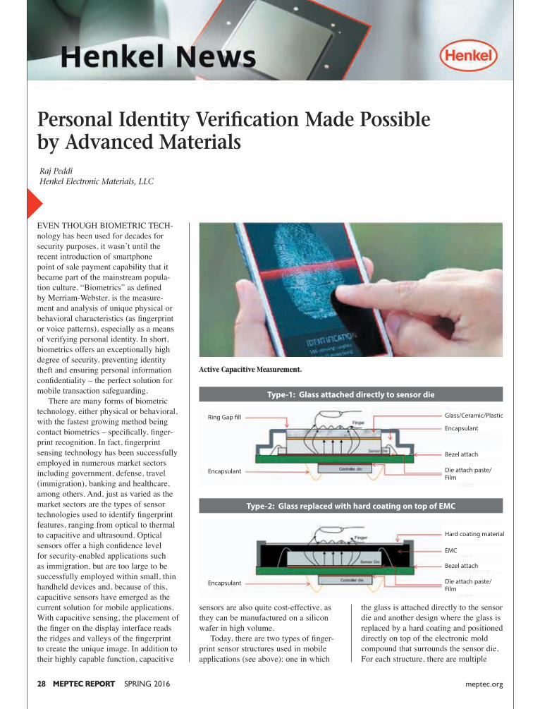
28 MEPTEC REPORT SPRING 2016 meptec.org
EVEN THOUGH BIOMETRIC TECH-nology has been used for decades for security purposes, it wasn’t until the recent introduction of smartphone point of sale payment capability that it became part of the mainstream popula-tion culture. “Biometrics” as defined by Merriam-Webster, is the measure-ment and analysis of unique physical or behavioral characteristics (as fingerprint or voice patterns), especially as a means of verifying personal identity. In short, biometrics offers an exceptionally high degree of security, preventing identity theft and ensuring personal information confidentiality – the perfect solution for mobile transaction safeguarding. There are many forms of biometric technology, either physical or behavioral, with the fastest growing method being contact biometrics – specifically, finger-print recognition. In fact, fingerprint sensing technology has been successfully employed in numerous market sectors including government, defense, travel (immigration), banking and healthcare, among others. And, just as varied as the market sectors are the types of sensor technologies used to identify fingerprint features, ranging from optical to thermal to capacitive and ultrasound. Optical sensors offer a high confidence level for security-enabled applications such as immigration, but are too large to be successfully employed within small, thin handheld devices and, because of this, capacitive sensors have emerged as the current solution for mobile applications. With capacitive sensing, the placement of the finger on the display interface reads the ridges and valleys of the fingerprint to create the unique image. In addition to their highly capable function, capacitive
the glass is attached directly to the sensor die and another design where the glass is replaced by a hard coating and positioned directly on top of the electronic mold compound that surrounds the sensor die. For each structure, there are multiple
sensors are also quite cost-effective, as they can be manufactured on a silicon wafer in high volume. Today, there are two types of finger-print sensor structures used in mobile applications (see above): one in which
Personal Identity Verification Made Possible by Advanced Materials Raj Peddi Henkel Electronic Materials, LLC
Active Capacitive Measurement.
Type-1: Glass attached directly to sensor die
Glass/Ceramic/Plastic
Encapsulant
Bezel attach
Die attach paste/ Film
Encapsulant
Ring Gap fill
Type-2: Glass replaced with hard coating on top of EMC
Hard coating material
EMC
Bezel attach
Die attach paste/ Film
Encapsulant
The smaller the device - the more solutionsNo matter where you are or what your process requires, you can count on Henkel‘s expertise. Our unmatched portfolio of advanced materials for the semiconductor and assembly markets all backed by the innovation, knowledge and support of Henkel‘s world-class global team ensures your success and guarantees a low-risk partnership proposition.
The smaller the device - the more solutionsNo matter where you are or what your process requires, you can count on Henkel‘s expertise. Our unmatched portfolio of advanced materials for the semiconductor and assembly markets all backed by the innovation, knowledge and support of Henkel‘s world-class global team ensures your success and guarantees a low-risk partnership proposition.
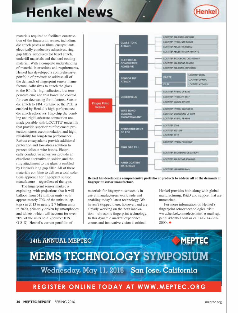
30 MEPTEC REPORT SPRING 2016 meptec.org
materials required to facilitate construc-tion of the fingerprint sensor, including: die attach pastes or films, encapsulants, electrically conductive adhesives, ring gap fillers, adhesives for bezel attach, underfill materials and the hard coating material. With a complete understanding of material interactions and requirements, Henkel has developed a comprehensive portfolio of products to address all of the demands of fingerprint sensor manu-facture. Adhesives to attach the glass to the IC offer high adhesion, low tem-perature cure and thin bond line control for ever-decreasing form factors. Sensor die attach to FR4, ceramic or the PCB is enabled by Henkel’s high-performance die attach adhesives. Flip-chip die bond-ing and rigid substrate connection are made possible with LOCTITE® underfills that provide superior reinforcement pro-tection, stress accommodation and high reliability for long-term performance. Robust encapsulants provide additional protection and low-stress solution to protect delicate wire bonds. Electri-cally conductive adhesives provide an excellent alternative to solder, and the ring attachment to the glass is enabled by Henkel’s ring gap filler. All of these materials combine to deliver a total solu-tions approach for fingerprint sensor manufacture – regardless of the type. The fingerprint sensor market is exploding, with projections that it will balloon from 512 million units (with approximately 70% of the units in lap-tops) in 2013 to nearly 2.7 billion units in 2020, primarily driven by smartphones and tablets, which will account for over 50% of the units sold. (Source: IHS, O-S-D). Henkel’s current portfolio of
Henkel provides both along with global manufacturing, R&D and support that are unmatched. For more information on Henkel’s fingerprint sensor technologies, visit www.henkel.com/electronics, e-mail [email protected] or call +1-714-368-8000. ◆
materials for fingerprint sensors is in use at manufacturers worldwide and enabling today’s latest technology. We haven’t stopped there, however, and are already working on the next innova-tion – ultrasonic fingerprint technology. In this dynamic market, experience counts and innovative vision is critical:
Henkel has developed a comprehensive portfolio of products to address all of the demands of fingerprint sensor manufacture.
MEMS TECHNOLOGY SYMPOSIUMWednesday, May 11, 2016 San Jose, California
14th ANNUAL MEPTEC
R E G I S T E R O N L I N E T O D A Y A T W W W . M E P T E C . O R G
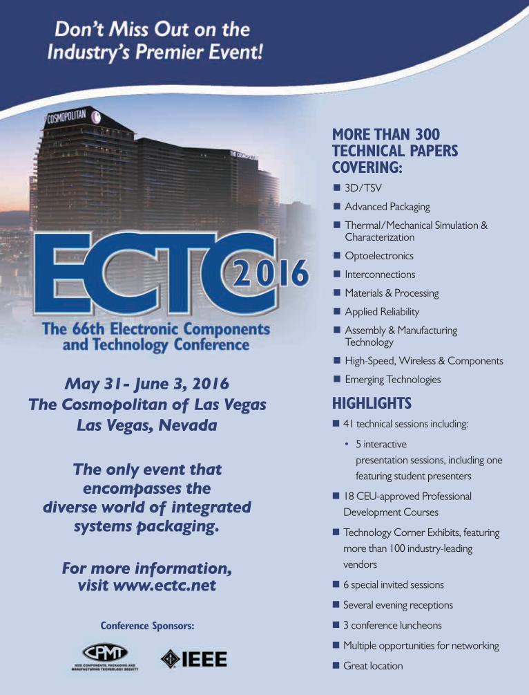
Conference Sponsors:
MORE THAN 300 TECHNICAL PAPERS COVERING:n3D/TSV
nAdvanced Packaging
nThermal/Mechanical Simulation & Characterization
nOptoelectronics
nInterconnections
nMaterials & Processing
nApplied Reliability
nAssembly & Manufacturing Technology
nHigh-Speed, Wireless & Components
nEmerging Technologies
HIGHLIGHTSn41 technical sessions including:
5 interactive presentation sessions, including one featuring student presenters
n18 CEU-approved Professional Development Courses
nTechnology Corner Exhibits, featuring more than 100 industry-leading vendors
n6 special invited sessions
nSeveral evening receptions
n3 conference luncheons
nMultiple opportunities for networking
nGreat location
May 31- June 3, 2016The Cosmopolitan of Las Vegas
Las Vegas, Nevada
The only event that encompasses the
diverse world of integrated systems packaging.
For more information, visit www.ectc.net
Packaging Technologies
PacTech - Packaging Technologiesis a worldwide leader in both WaferLevel Bumping & Packaging Servicesand in Advanced Packaging Equipment Manufacturing.
32 MEPTEC REPORT SPRING 2016 meptec.org
ALMOST 40 KILOMETERS NORTH-west of Germany’s capital, Berlin, is the city of Nauen where PacTech has its headquarters. Founded as a spin-off of the federal scientific Fraunhofer IZM in 1995, the company consists of two busi-ness units:
1. Manufacturer of advanced wafer level packaging and wafer bumping production equipment.
2. Provider of high-quality, subcontract manufacturing services.
With subsidiaries in California and Malaysia, the corporation supplies its outstanding solutions in these relevant business regions. PacTech has continually grown, and the company is to date the biggest high-tech employer in the region with a staff of some 350 people. In Europe, the U.S. and Malaysia, the full enterprise portfolio of differ-ent manufacturing services is available, as well as all of the backend solutions. The advanced equipment manufacturing operations is located at the German HQ. All machinery, sold originates from the headquarters and carries the well-known brand: “Made in Germany”! The company’s main target area is now the Asian markets, which consume the lion’s share of products and services. With more than 20 years of experi-ence, PacTech is a prime manufacturer of leading-edge technology equipment and
The electro-less plating line addresses applications in power MOSFET devices for clip attach, contactless RFID devices, high reliability power devices, and for Wire Bonding applications using Ni/Au, Ni/Pd respectively, including Ni/Pd/Au for Over Pad Metallization, and many other applications. Ni/Pd Metallization is qualified for volume production of low cost Cu Wire Bonding over active pad. The new Ultra SB² tool is address-ing all wafer and substrate-related solder ball applications for high volume mass production. PacTech has leading edge technology for Solder Ball Transfer, Minimum Solder Ball diameter is 30 µm. For the electro-less Plating Tool, PacTech is the worldwide leader with more than 20 Automatic Tools installed worldwide. Since its inception, PacTech has received more than 110 patents for prod-ucts developed in areas relating to wafer bumping, flip-chip and chip-scale pack-aging, and laser-bonding technology. Also PacTech is providing all chemi-cals for wet Chemical Pad Protection and Pad Metallization as part of a turnkey solution for electro-less Wafer Bumping. Additional analytical services and sup-port to customers is available. It is PacTech’s mission to provide the highest level of innovative technology solutions with an unparalleled degree of customer service orientation, corporate integrity and attention to its clients’ indi-vidual technology demands. More information is available at the PacTech website at www.pactech.de. ◆
processes for the advanced packaging industry. PacTech designs, manufactures and supports solder jetting equipment, wafer-level solder ball transfer systems, wafer-level solder rework equipment, laser assisted flip-chip bonders and automatic plating tools for high volume electro-less Ni/Au and Ni/Pd/Au Under Bump Metallurgy (UBM) and Over Pad Metallurgy (OPM) through its global sales network. In its worldwide sales and applica-tion centers PacTech offers demonstra-tion capabilities, including assembly of samples and prototyping under ISO certified production conditions. More-over, PacTech has a unique dual business model in which it offers its customers with new chip designs or initial low vol-ume requirements the option to use in the initial phase PacTech’s demo centers for services. After qualification of the prod-uct the customer has the option of further cost reduction by utilizing PacTech’s full turnkey solution: Equipment, Process and Technology. This reduces the cost of customers new product introductions and at the same time gives the customer the option to qualify and intensively study the technology, and understand the cost of ownership. Together with its partner and main shareholder NAGASE, PacTech is also developing embedding technologies for wafer and substrate level CSP technologies. The solder ball jetting equipment addresses markets like Hard Disk Drive, Camera Module, Sen-sors and Stacked TSV chip packages.
Prime Manufacturer of Leading-edge Technology Equipment & Processes for the Advanced Packaging Industry
[email protected] 9001
ISO TS 16949ISO 14001
Your Partner forAdvanced Packaging
Our Services
Wafer Bumping- UBM & OPM Plating, e.g. eless NiAu & NiPdAu, e-plate Cu & Au- NiFe Plating for MEMS- Solder Ball Attach / Solder Jetting- Wafer Level RDL (Low Volume)- CSP & BGA Ball Rework
Wafer Backside Metallization- Wafer Thinning- Single Wafer Etch- TiNiAg & TiNiAu Evaporation
Backend & Die Sort- Laser Marking, Sawing, Electrical Test- Tape & Reel- FC-Assembly
soft to take a greater role in data center architectures and chip design to support their needs. To realize these optimistic expecta-tions for meaningful growth, innovation and entrepreneurship generally associ-ated with startups are even more crucial. However, all indicators ranging from IPOs, venture capital investment, and organic industry growth rates strongly suggest that new business models are needed. Taking inspiration from the robust incubation and acquisition activities in software, pharmaceuticals and biotech, a new approach to assist startups pursuing solutions in silicon has been launched. Its unique focus is on the difficult prob-lems entrepreneurs and new companies encounter when attempting to innovate in semiconductors and MEMS, namely the challenge of raising sufficient fund-ing and obtaining the appropriate design, prototyping, and test capabilities to move from concept to working prototypes. In this context, I am now part of an early-stage startup incubator called Silicon Catalyst, launched in 2015. The objective is to stimulate a vital and robust startup community by connecting the interests of the industry stakeholders, ranging from systems and product-based companies to the enabling supply chain, to a network of mentors experienced in assisting startups, and to investors who are looking for attractive returns and timely graduation and acquisition. Since opening its doors, Silicon Cata-lyst has seen over 70 startups apply for admission. The companies cover a wide gamut ranging from data center applica-tions, wearables, energy harvesting, loca-tion awareness and biomedical applica-tions in addition to traditional semicon-ductors ranging from enhanced memory solutions to deep learning applications. These startups are mostly driven by new
OPINION
AS A PACKAGING TECHNOLOGIST for most of my career, I have had the opportunity to deploy multiple new packaging technologies that mirrored the growth of semiconductor industry as it evolved from the era of integrated device manufacturers to the era of specializa-tion with the rise of foundries and fabless companies to today’s structure character-ized by consolidation and dominance by a few leaders in each product area. Over the last few years, the slowdown in innovation in the semiconductor indus-try is becoming increasingly evident. One of the main reasons ascribed to this slowdown is the technical and financial challenges sustaining Moore’s law, there-by creating an economic squeeze play for the industry. The industry response has been to circle the wagons and go through an extraordinary $130 plus billion merg-ers and acquisition activity over the past 12-16 months. This activity is primarily driven by the need to streamline costs and align portfolios to increase profits. The impact of this trend on industry R&D and overall innovation is an active conversation topic in the industry and provides an opportunity for the emer-gence of alternative innovation pipelines. At the same time, there is anticipation of a new wave of innovation associ-ated with key trends in energy, personal health care, autonomous transportation, mobility, and home automation, gener-ally referred to as the Internet of Things (IoT). In addition, the rise of cloud based computing, driven by the need to analyze increasingly massive amounts of data is also driving innovation in semicon-ductors. These innovations will require a significant rethinking around chip architecture itself, from the traditional logic focused to memory focus. This is evidenced by recent efforts at Alphabet (Google), Amazon, Facebook and Micro-
entrepreneurs – some from universities and some from the industry – who have recognized the realities of the current environment and are looking for an alter-native. It is heartening to see that there is a still a vibrant startup community out there. Over the coming years, I expect spinoffs from merged and acquired com-panies will provide another source of exciting semiconductor startups as well. Many other geographies outside of Sili-con Valley are also looking to create and expand their semiconductor industry and they are actively encouraging startups, another promising sign. These startups provide an exciting opportunity for the MEPTEC community to get involved in this next growth wave of semiconductors. It is well recognized that packaging is an increasingly critical component of the value proposition for most of these startups, especially as they strive for innovative solutions to address the diverse markets they plan to serve. Most startups need to consider upfront packaging and supply chain consider-ations to ensure a viable product espe-cially in the SIP and MEMS arena. Most entrepreneurs have limited experience in the backend aspects of semiconductor design and manufacturing. They recog-nize that and they appreciate and need the support of the MEPTEC community. Our vision at Silicon Catalyst is that in the coming years, small teams innovating meaningful solutions using custom silicon will be considered “cool” and will launch another growth wave like the rise of the foundry and fabless model did in the ‘90s, revitalizing the semicon-ductor industry once again. As we say in our tagline, we’re bringing silicon back to Silicon Valley and we encourage you to do your part in bringing it back to its roots. ◆
Enabling the Next Growth Wave for SemiconductorsA New Approach to Enable Innovative Startups
34 MEPTEC REPORT SPRING 2016 meptec.org
Tarun Verma, Partner Silicon Catalyst
Customer demand for highly sophisticated products has made semiconductor packaging an important factor in system performance. As one of the world’s largest suppliers of outsourced semiconductor packaging design, assembly and test services, Amkor helps make “next generation” products a reality.
Founded in 1968, Amkor’s continuous path of innovation, improvement and growth has led us to be a strategic and trusted manufacturing partner for many of the world’s leading semiconductor companies. As the industry moves aggressively
toward new and more complex technologies, our unique expertise in high-volume
manufacturing techniques and the ability to solve technological challenges
are among our greatest strengths.
Customers also benefit from our extensive and
expanding global footprint, enabling
us to easily handle large orders and offer quick turnaround times. Amkor is positioned to deliver end-to-end solutions that meet the requirements for a broad range of product
designs today, and in the
future.
www.amkor.com
Connecting People and Technology
Perfection Products Inc.1320 S. Indianapolis Ave. • Lebanon, IN 46052Phone: (765) 482-7786 • Fax: (765) 482-7792
Check out our Website: www.perfection-products.comEmail: [email protected]
Grip Ring Shippers
I. C. Trays - Multi-Channel
Lead Frame Magazines - F.O.L./E.O.L.
Film Frame Magazines
Film Frames Film Frame Shippers
TO Tapes & Magazines
Magazines and Carriers for Process Handling Solutions
Accept Nothing Less.
Substrate Carrier Magazines
Stack Magazines - E.O.L.
Wafer Carriers
Process Carriers (Boats)
Boat Magazines
Grip Rings
Miscellaneous Magazines
I. C. Tubes and Rails
Grip Ring Magazines